Embed Size (px)
Citation preview
Digital Microelectronic Circuits The VLSI Systems Center - BGU Lecture 4: The CMOS Inverter 1
Digital Microelectronic
Circuits
(361-1-3021 )
The CMOS Inverter
Presented by: Adam Teman
Lecture 4:
Digital Microelectronic Circuits The VLSI Systems Center - BGU Lecture 4: The CMOS Inverter
Last Lectures
Moore’s Law
Terminology
» Static Properties
» Dynamic Properties
» Power
The MOSFET Transistor
» Shockley Model
» Channel Length Modulation, Velocity Saturation,
Body Effect
2
Digital Microelectronic Circuits The VLSI Systems Center - BGU Lecture 4: The CMOS Inverter
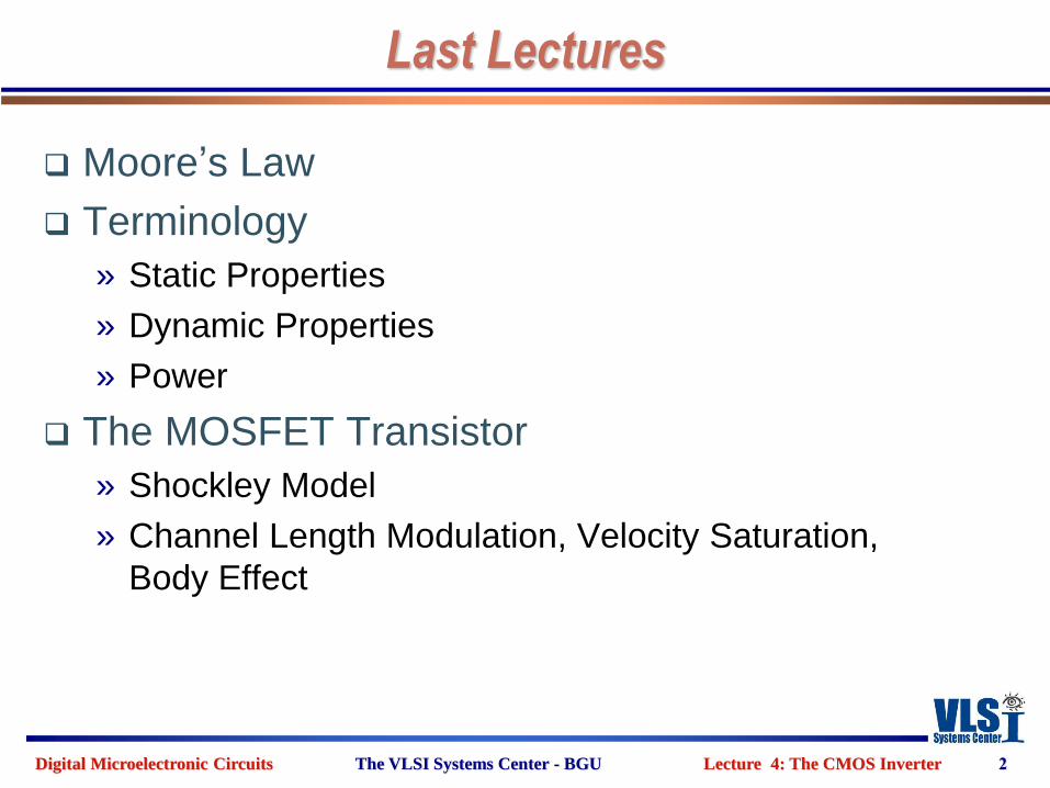
This Week - Motivation
The Inverter, or NOT gate, is truly the
nucleus of all digital designs.
We will analyze the inverter and find its
characterizing parameters.
Once its operation and properties are
clearly understood, designing and
analyzing more intricate structures, such
as NAND gates, adders, multipliers and
microprocessors is greatly simplified.
This lecture focuses on the static CMOS
inverter – the most popular at present and
the basis for the CMOS digital logic family.
3
In Out
0 1
1 0
In Out
Digital Microelectronic Circuits The VLSI Systems Center - BGU Lecture 4: The CMOS Inverter
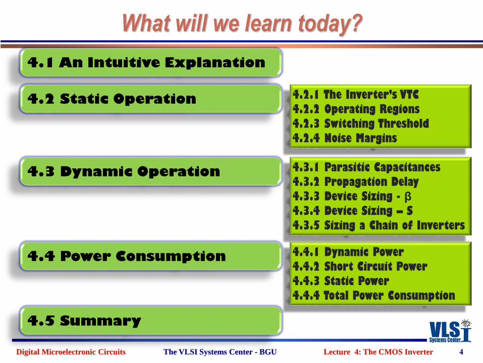
What will we learn today?
4
4.1 An Intuitive Explanation
4.2 Static Operation
4.3 Dynamic Operation
4.4 Power Consumption
4.5 Summary
4.2.1 The Inverter’s VTC
4.2.2 Operating Regions
4.2.3 Switching Threshold
4.2.4 Noise Margins
4.3.1 Parasitic Capacitances
4.3.2 Propagation Delay
4.3.3 Device Sizing - β
4.3.4 Device Sizing – S
4.3.5 Sizing a Chain of Inverters
4.4.1 Dynamic Power
4.4.2 Short Circuit Power
4.4.3 Static Power
4.4.4 Total Power Consumption
Digital Microelectronic Circuits The VLSI Systems Center - BGU Lecture 4: The CMOS Inverter
AN INTUITIVE EXPLANATION
As usual, we’ll start with
5
4.14.1 An Intuitive Explanation
4.2 Static Operation
4.3 Dynamic Operation
4.4 Power Consumption
4.5 Summary
Digital Microelectronic Circuits The VLSI Systems Center - BGU Lecture 4: The CMOS Inverter
+
-
V
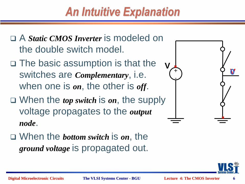
An Intuitive Explanation
A Static CMOS Inverter is modeled on
the double switch model.
The basic assumption is that the
switches are Complementary, i.e.
when one is on, the other is off.
When the top switch is on, the supply
voltage propagates to the output
node.
When the bottom switch is on, the
ground voltage is propagated out.
6
V0
Digital Microelectronic Circuits The VLSI Systems Center - BGU Lecture 4: The CMOS Inverter
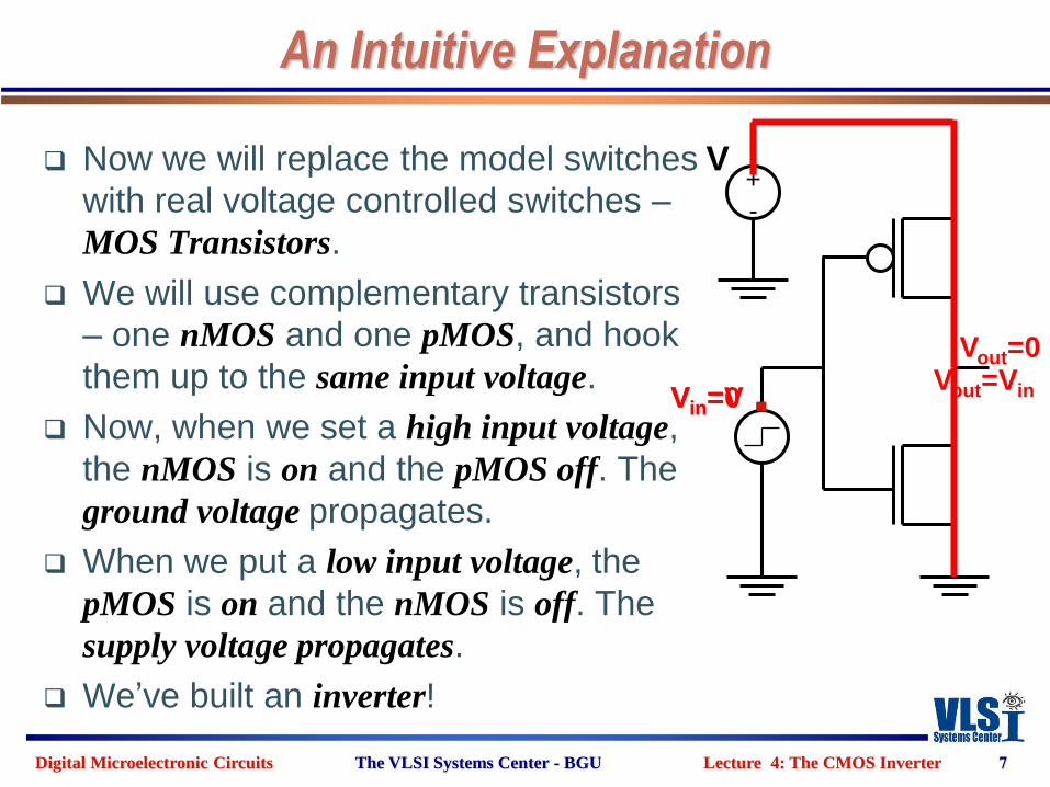
An Intuitive Explanation
Now we will replace the model switches
with real voltage controlled switches –
MOS Transistors.
We will use complementary transistors
– one nMOS and one pMOS, and hook
them up to the same input voltage.
Now, when we set a high input voltage,
the nMOS is on and the pMOS off. The
ground voltage propagates.
When we put a low input voltage, the
pMOS is on and the nMOS is off. The
supply voltage propagates.
We’ve built an inverter!
7
Vin=V
+
-
V
Vout=0
Vin=0Vout=Vin
Digital Microelectronic Circuits The VLSI Systems Center - BGU Lecture 4: The CMOS Inverter
An Intuitive Explanation
The voltage connected to the Source of the pMOS is
known as the “Supply Voltage” or VDD.*
We mark the connection to VDD with a horizontal or
slanted bar.
Accordingly, VDD represents a logical ‘1’ and GND
represents a logical ‘0’.
Inputting VDD to the CMOS inverter will present GND
at the output. Inputting GND will present VDD at the
output.
This characteristic is non-trivial and is one of the
advantages of CMOS design. It is known as “Rail to
Rail Swing”.**
8
* It can also be called VCC, regarding the Collector of BJT transistors.
** “Rails” are the supply voltages, i.e. VDD and GND. If a voltage is connected
to the nMOS Source instead of GND, we refer to this voltage as VSS.
Digital Microelectronic Circuits The VLSI Systems Center - BGU Lecture 4: The CMOS Inverter
STATIC OPERATION
Now that we understand the principles,
we’ll analyze
9
4.24.1 An Intuitive Explanation
4.2 Static Operation
4.3 Dynamic Operation
4.4 Power Consumption
4.5 Summary
Digital Microelectronic Circuits The VLSI Systems Center - BGU Lecture 4: The CMOS Inverter
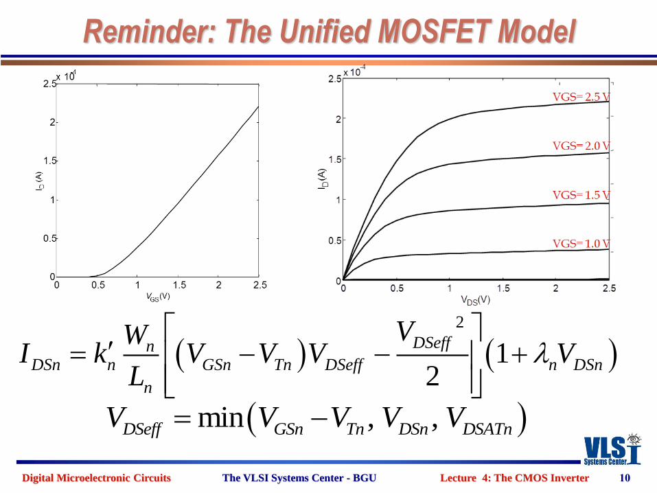
Reminder: The Unified MOSFET Model
10
min , ,DSeff GSn Tn DSn DSATnV V V V V
2
12
DSeffnDSn n GSn Tn DSeff n DSn
n
VWI k V V V V
L
Digital Microelectronic Circuits The VLSI Systems Center - BGU Lecture 4: The CMOS Inverter
Reminder: Static Properties
VTC
Noise Margins
11
Digital Microelectronic Circuits The VLSI Systems Center - BGU Lecture 4: The CMOS Inverter
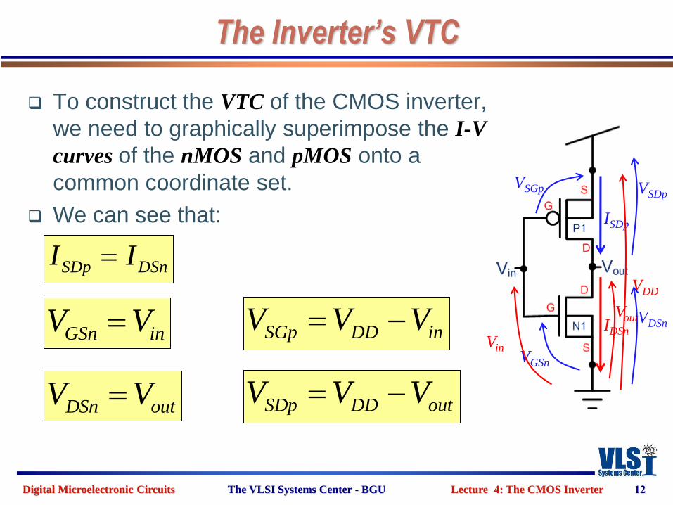
The Inverter’s VTC
To construct the VTC of the CMOS inverter,
we need to graphically superimpose the I-V
curves of the nMOS and pMOS onto a
common coordinate set.
We can see that:
12
ISDp
IDSn
SDp DSnI I
GSn inV V SGp DD inV V V
DSn outV V SDp DD outV V V
VGSn
Vout
VSGp
Vin
VDD
VDSn
VSDp
Digital Microelectronic Circuits The VLSI Systems Center - BGU Lecture 4: The CMOS Inverter
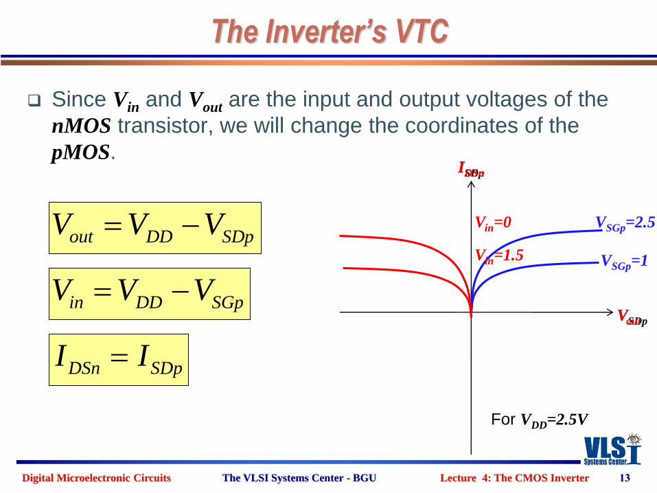
The Inverter’s VTC
Since Vin and Vout are the input and output voltages of the
nMOS transistor, we will change the coordinates of the
pMOS.
13
VSGp=2.5
VSGp=1
out DD SDpV V V
ISDp
VSDp
Vin=1.5
Vin=0
IDSn
DSn SDpI I
Vout
in DD SGpV V V
For VDD=2.5V

Digital Microelectronic Circuits The VLSI Systems Center - BGU Lecture 4: The CMOS Inverter
The Inverter’s VTC
Now, we will superimpose the modified pMOS I-V curves on
the nMOS I-V graphs:
14
Vout
IDSn
Vin=0
Vin=0
Vin=VDD/2Vin=VDD/2
Vin=VDD
Vin=VDD
The intersection of corresponding load lines shows the DC
operating points, where the currents of the nMOS and pMOS
are equal.
Digital Microelectronic Circuits The VLSI Systems Center - BGU Lecture 4: The CMOS Inverter
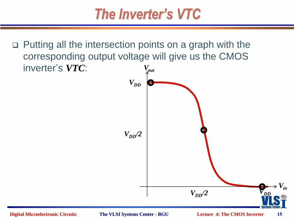
The Inverter’s VTC
Putting all the intersection points on a graph with the
corresponding output voltage will give us the CMOS
inverter’s VTC:
15
Vout
Vin
VDD
VDD/2
VDD/2 VDD
Digital Microelectronic Circuits The VLSI Systems Center - BGU Lecture 4: The CMOS Inverter
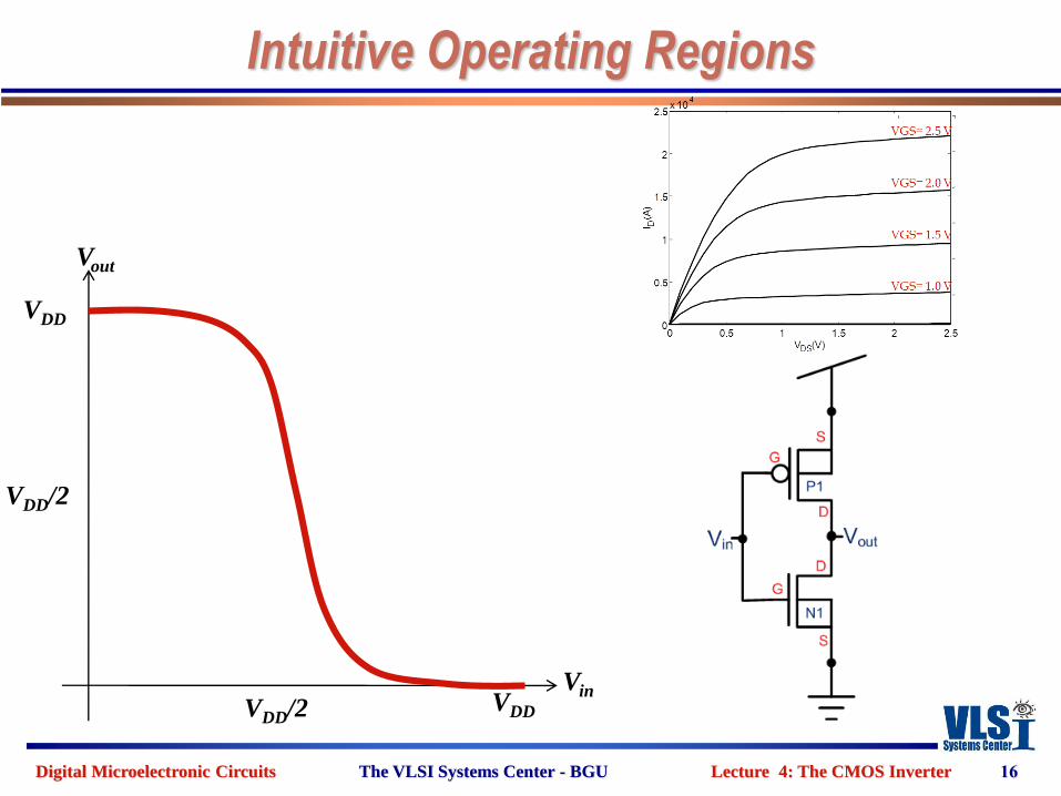
Intuitive Operating Regions
16
Vout
Vin
VDD
VDD/2
VDD/2 VDD
Digital Microelectronic Circuits The VLSI Systems Center - BGU Lecture 4: The CMOS Inverter
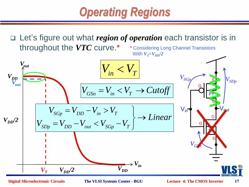
Operating Regions
Let’s figure out what region of operation each transistor is in
throughout the VTC curve.*
17
Vout
Vin
VDD
VDD/2
VDD/2 VDD
* Considering Long Channel Transistors
With VT<VDD/2
VT
in TV V
GSn in TV V V Cutoff
VGSn
SGp DD in T
SDp DD out SGp T
V V V VLinear
V V V V V
VSGp VSDpVout
Digital Microelectronic Circuits The VLSI Systems Center - BGU Lecture 4: The CMOS Inverter
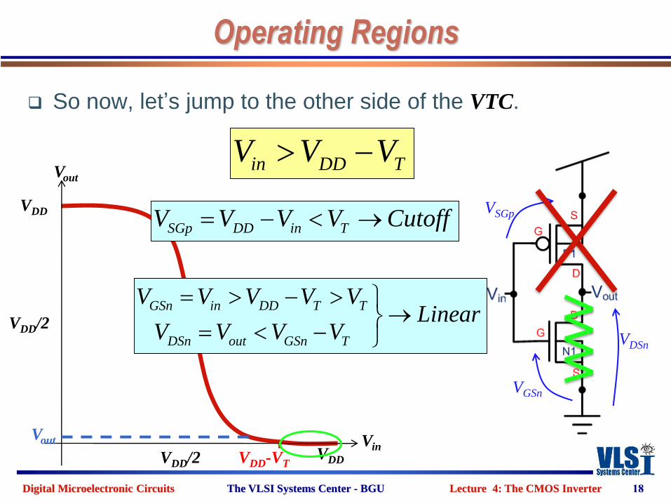
Operating Regions
So now, let’s jump to the other side of the VTC.
18
Vout
Vin
VDD
VDD/2
VDD/2 VDDVDD-VT
in DD TV V V
SGp DD in TV V V V Cutoff
VGSn
GSn in DD T T
DSn out GSn T
V V V V VLinear
V V V V
VSGp
VDSn
Vout
Digital Microelectronic Circuits The VLSI Systems Center - BGU Lecture 4: The CMOS Inverter
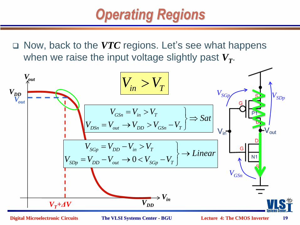
Operating Regions
Now, back to the VTC regions. Let’s see what happens
when we raise the input voltage slightly past VT.
19
Vout
Vin
VDD
VDDVT+ΔV
in TV V
GSn in T
DSn out DD GSn T
V V VSat
V V V V V
VGSn
0
SGp DD in T
SDp DD out SGp T
V V V VLinear
V V V V V
VSGp VSDpVout
Digital Microelectronic Circuits The VLSI Systems Center - BGU Lecture 4: The CMOS Inverter
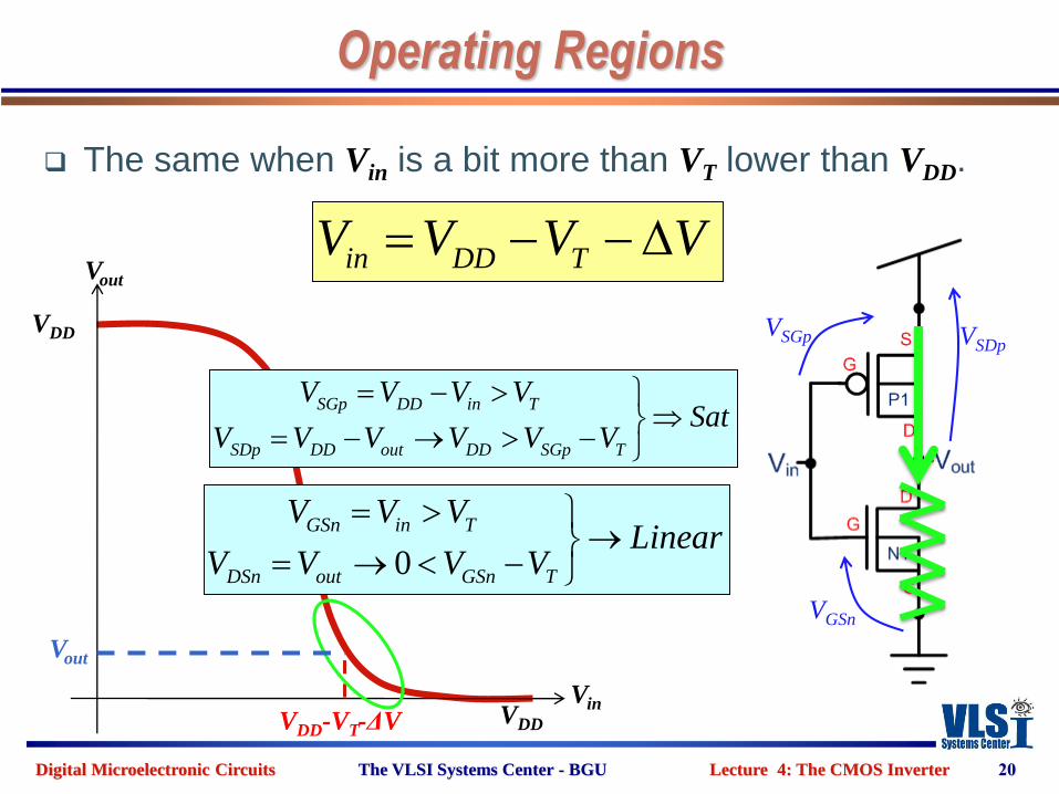
Operating Regions
The same when Vin is a bit more than VT lower than VDD.
20
Vout
Vin
VDD
VDDVDD-VT-ΔV
in DD TV V V V
SGp DD in T
SDp DD out DD SGp T
V V V VSat
V V V V V V
VGSn
0
GSn in T
DSn out GSn T
V V VLinear
V V V V
VSGp VSDp
Vout
Digital Microelectronic Circuits The VLSI Systems Center - BGU Lecture 4: The CMOS Inverter
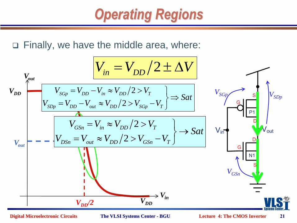
Operating Regions
Finally, we have the middle area, where:
21
Vout
Vin
VDD
VDDVDD/2
2in DDV V V
2
2
SGp DD in DD T
SDp DD out DD SGp T
V V V V VSat
V V V V V V
VGSn
VSGp VSDp
Vout
2
2
GSn in DD T
DSn out DD GSn T
V V V VSat
V V V V V
Digital Microelectronic Circuits The VLSI Systems Center - BGU Lecture 4: The CMOS Inverter
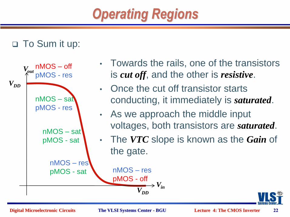
Operating Regions
To Sum it up:
22
Vout
Vin
VDD
VDD
• Towards the rails, one of the transistors
is cut off, and the other is resistive.
• Once the cut off transistor starts
conducting, it immediately is saturated.
• As we approach the middle input
voltages, both transistors are saturated.
• The VTC slope is known as the Gain of
the gate.
nMOS – off
pMOS - res
nMOS – sat
pMOS - res
nMOS – sat
pMOS - sat
nMOS – res
pMOS - sat nMOS – res
pMOS - off
Digital Microelectronic Circuits The VLSI Systems Center - BGU Lecture 4: The CMOS Inverter
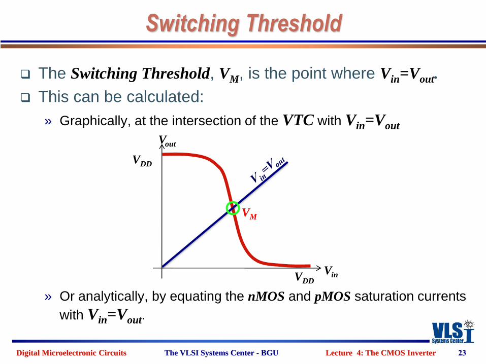
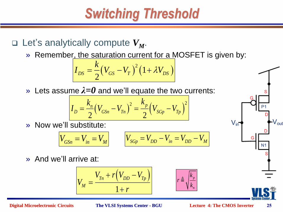
Switching Threshold
The Switching Threshold, VM, is the point where Vin=Vout.
This can be calculated:
» Graphically, at the intersection of the VTC with Vin=Vout
» Or analytically, by equating the nMOS and pMOS saturation currents
with Vin=Vout.
23
Vout
Vin
VDD
VDD
VM
Digital Microelectronic Circuits The VLSI Systems Center - BGU Lecture 4: The CMOS Inverter
Switching Threshold
But let’s start with the intuitive approach…
24
Digital Microelectronic Circuits The VLSI Systems Center - BGU Lecture 4: The CMOS Inverter
Switching Threshold
Let’s analytically compute VM.
» Remember, the saturation current for a MOSFET is given by:
» Lets assume λ=0 and we’ll equate the two currents:
» Now we’ll substitute:
» And we’ll arrive at:
25
22
2 2
pnD GSn Tn SGp Tp
kkI V V V V
2
12
DS GS T DS
kI V V V
GSn in MV V V SGp DD in DD MV V V V V
1
Tn DD Tp
M
V r V VV
r
p
n
kr
k
Digital Microelectronic Circuits The VLSI Systems Center - BGU Lecture 4: The CMOS Inverter
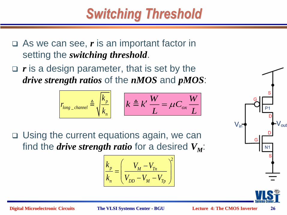
Switching Threshold
As we can see, r is an important factor in
setting the switching threshold.
r is a design parameter, that is set by the
drive strength ratios of the nMOS and pMOS:
Using the current equations again, we can
find the drive strength ratio for a desired VM:
26
_
p
long channel
n
kr
kox
W Wk k C
L L
2
p M Tn
n DD M Tp
k V V
k V V V
Digital Microelectronic Circuits The VLSI Systems Center - BGU Lecture 4: The CMOS Inverter
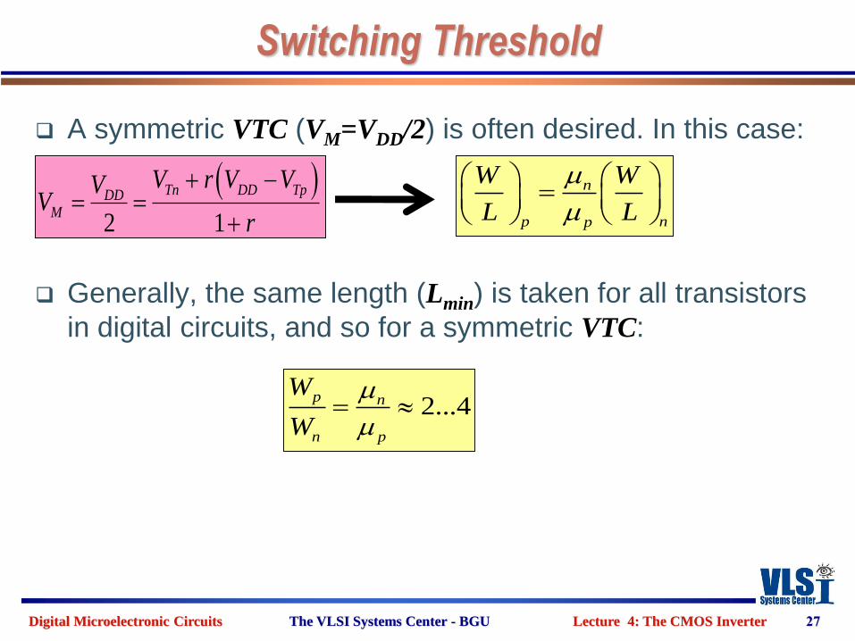
Switching Threshold
A symmetric VTC (VM=VDD/2) is often desired. In this case:
Generally, the same length (Lmin) is taken for all transistors
in digital circuits, and so for a symmetric VTC:
27
n
p np
W W
L L
2...4p n
n p
W
W
2 1
Tn DD TpDDM
V r V VVV
r
Digital Microelectronic Circuits The VLSI Systems Center - BGU Lecture 4: The CMOS Inverter
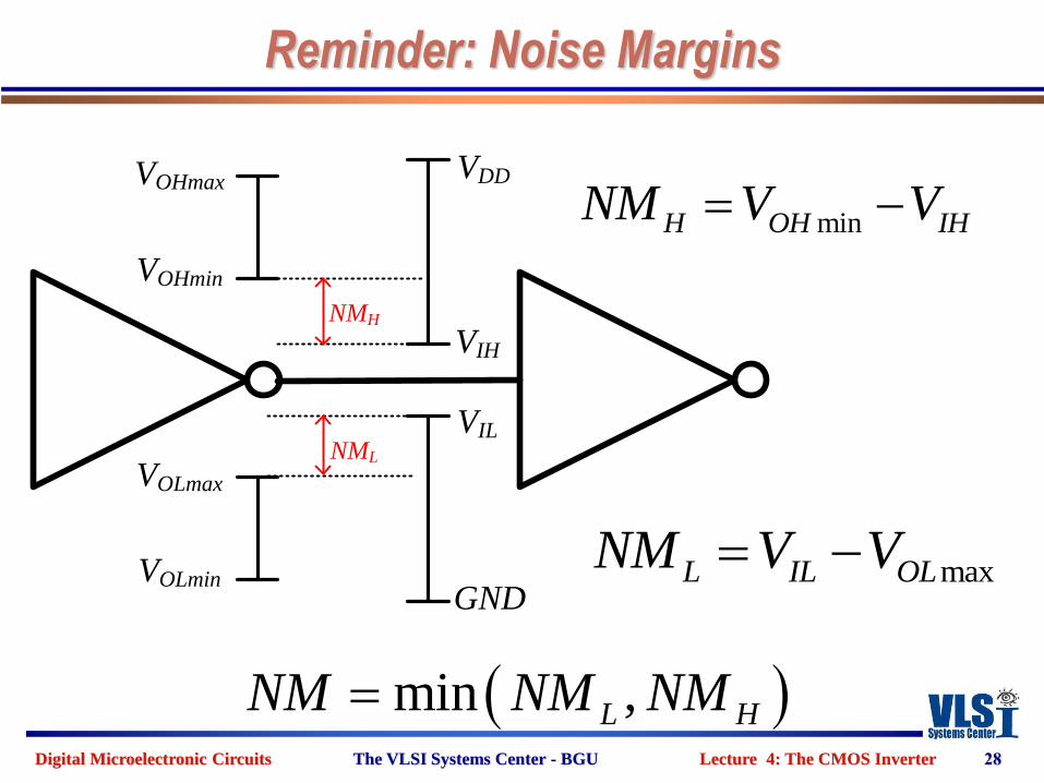
Reminder: Noise Margins
28
VOHmax
VOHmin
VOLmax
VOLmin
VDD
VIH
VIL
GND
NMH
NML
minH OH IHNM V V
maxL IL OLNM V V
min ,L HNM NM NM
Digital Microelectronic Circuits The VLSI Systems Center - BGU Lecture 4: The CMOS Inverter
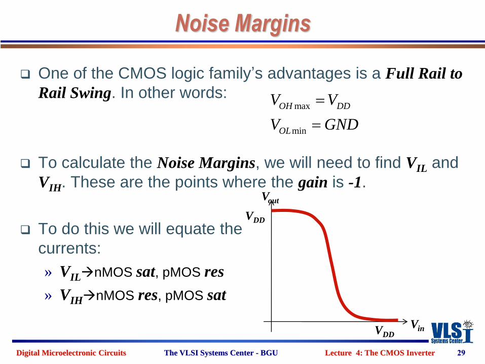
Noise Margins
One of the CMOS logic family’s advantages is a Full Rail to
Rail Swing. In other words:
To calculate the Noise Margins, we will need to find VIL and
VIH. These are the points where the gain is -1.
To do this we will equate the
currents:
» VILnMOS sat, pMOS res
» VIHnMOS res, pMOS sat
29
max
min
OH DD
OL
V V
V GND
Vout
Vin
VDD
VDD
Digital Microelectronic Circuits The VLSI Systems Center - BGU Lecture 4: The CMOS Inverter
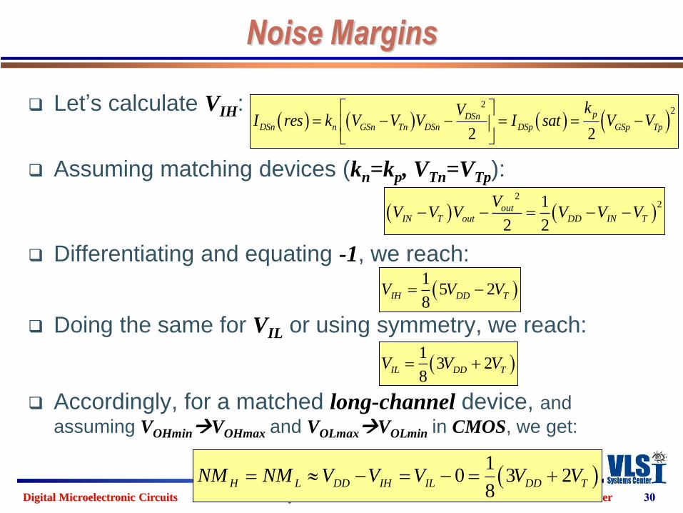
Noise Margins
Let’s calculate VIH:
Assuming matching devices (kn=kp, VTn=VTp):
Differentiating and equating -1, we reach:
Doing the same for VIL or using symmetry, we reach:
Accordingly, for a matched long-channel device, and
assuming VOHminVOHmax and VOLmaxVOLmin in CMOS, we get:
30
2
2
2 2
pDSnDSn n GSn Tn DSn DSp GSp Tp
kVI res k V V V I sat V V
2
21
2 2
outIN T out DD IN T
VV V V V V V
1
5 28
IH DD TV V V
1
3 28
IL DD TV V V
1
0 3 28
H L DD IH IL DD TNM NM V V V V V
Digital Microelectronic Circuits The VLSI Systems Center - BGU Lecture 4: The CMOS Inverter
Noise Margins
The previous analysis “assumed” many things and
therefore SHOULD NOT be memorized.
Let us look at the noise margins intuitively to try
and understand trade offs:
31
Digital Microelectronic Circuits The VLSI Systems Center - BGU Lecture 4: The CMOS Inverter
Summary of Static Properties
When Vin<VT or Vin>VDD-VT, one of the networks
(PUN/PDN) is off, providing Rail to Rail Swing.
The skew of the VTC is set by the sizing ratio
between the PUN and PDN.
Analytic Noise Margin calculation is rigorous and
approximation should be used when possible.
32

Digital Microelectronic Circuits The VLSI Systems Center - BGU Lecture 4: The CMOS Inverter
DYNAMIC OPERATION
Now that we see how the inverter behaves in
steady state, we will analyze it’s transient:
33
4.34.1 An Intuitive Explanation
4.2 Static Operation
4.3 Dynamic Operation
4.4 Power Consumption
4.5 Summary
Digital Microelectronic Circuits The VLSI Systems Center - BGU Lecture 4: The CMOS Inverter
Reminder: Dynamic Properties
Propagation Delay
Rise/Fall Time
34
Digital Microelectronic Circuits The VLSI Systems Center - BGU Lecture 4: The CMOS Inverter
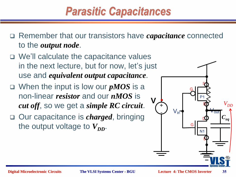
Parasitic Capacitances
Remember that our transistors have capacitance connected
to the output node.
We’ll calculate the capacitance values
in the next lecture, but for now, let’s just
use and equivalent output capacitance.
When the input is low our pMOS is a
non-linear resistor and our nMOS is
cut off, so we get a simple RC circuit.
Our capacitance is charged, bringing
the output voltage to VDD.
35
+
-
V
Ceq
VDD
Digital Microelectronic Circuits The VLSI Systems Center - BGU Lecture 4: The CMOS Inverter
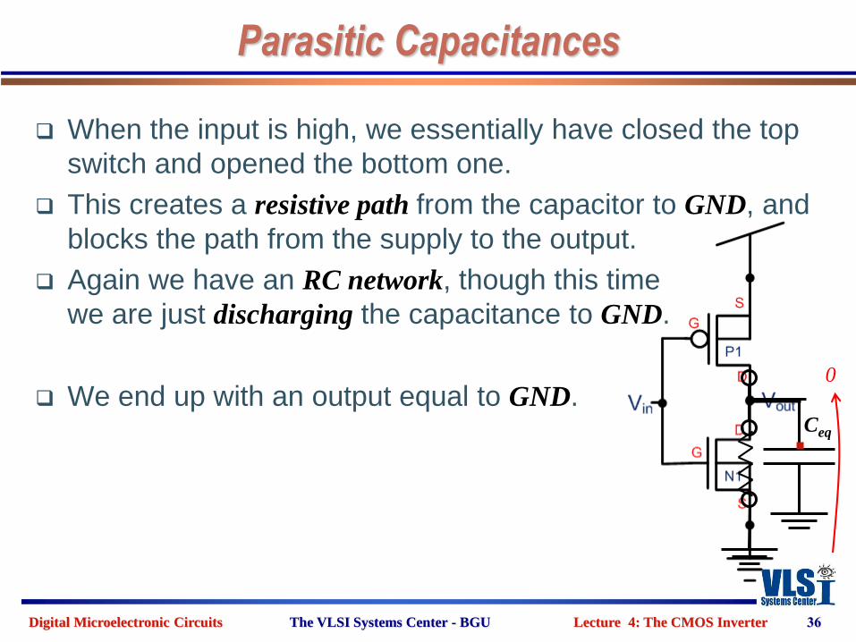
When the input is high, we essentially have closed the top
switch and opened the bottom one.
This creates a resistive path from the capacitor to GND, and
blocks the path from the supply to the output.
Again we have an RC network, though this time
we are just discharging the capacitance to GND.
We end up with an output equal to GND.
Parasitic Capacitances
36
Ceq
0
Digital Microelectronic Circuits The VLSI Systems Center - BGU Lecture 4: The CMOS Inverter
Parasitic Capacitances
So we saw that, a switching CMOS inverter charges and
discharges a parasitic output capacitance.
During the switching process, we can create a model that
will transform the circuit into a simple RC network.
In this way, we can easily derive a first order analysis of the
CMOS dynamic operation for propagation delay and power
consumption calculation.
37
Digital Microelectronic Circuits The VLSI Systems Center - BGU Lecture 4: The CMOS Inverter
Parasitic Capacitances
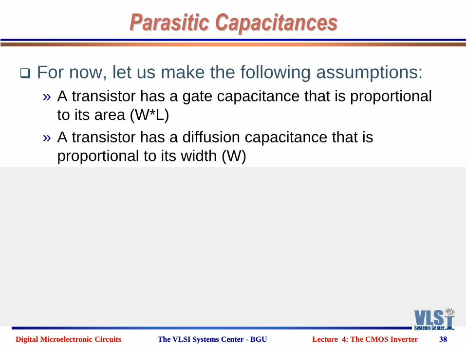
For now, let us make the following assumptions:
» A transistor has a gate capacitance that is proportional
to its area (W*L)
» A transistor has a diffusion capacitance that is
proportional to its width (W)
38
Digital Microelectronic Circuits The VLSI Systems Center - BGU Lecture 4: The CMOS Inverter
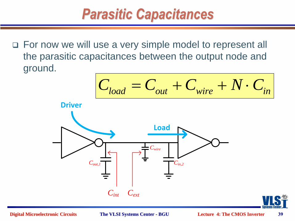
Parasitic Capacitances
For now we will use a very simple model to represent all
the parasitic capacitances between the output node and
ground.
39
Driver
Load
Cint Cext
Cwire
Cin,2Cout,1
load out wire inC C C N C
Digital Microelectronic Circuits The VLSI Systems Center - BGU Lecture 4: The CMOS Inverter
Propagation Delay
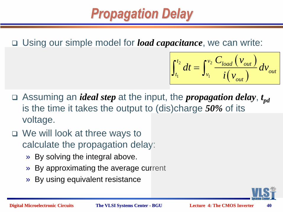
Using our simple model for load capacitance, we can write:
Assuming an ideal step at the input, the propagation delay, tpd
is the time it takes the output to (dis)charge 50% of its
voltage.
We will look at three ways to
calculate the propagation delay:
» By solving the integral above.
» By approximating the average current
» By using equivalent resistance
40
2 2
1 1
t vload out
outt v
out
C vdt dv
i v
Digital Microelectronic Circuits The VLSI Systems Center - BGU Lecture 4: The CMOS Inverter
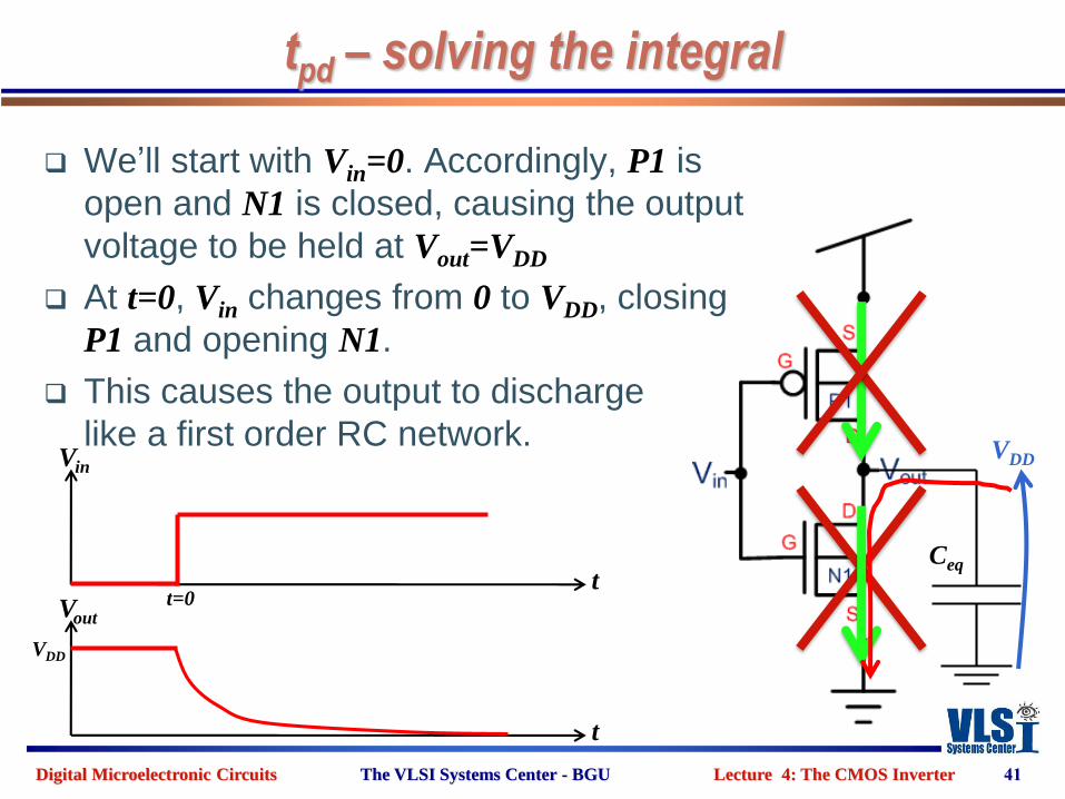
tpd – solving the integral
We’ll start with Vin=0. Accordingly, P1 is
open and N1 is closed, causing the output
voltage to be held at Vout=VDD
At t=0, Vin changes from 0 to VDD, closing
P1 and opening N1.
This causes the output to discharge
like a first order RC network.
41
VDD
Ceqt
Vin
t
Voutt=0
VDD
Digital Microelectronic Circuits The VLSI Systems Center - BGU Lecture 4: The CMOS Inverter
tpd – solving the integral
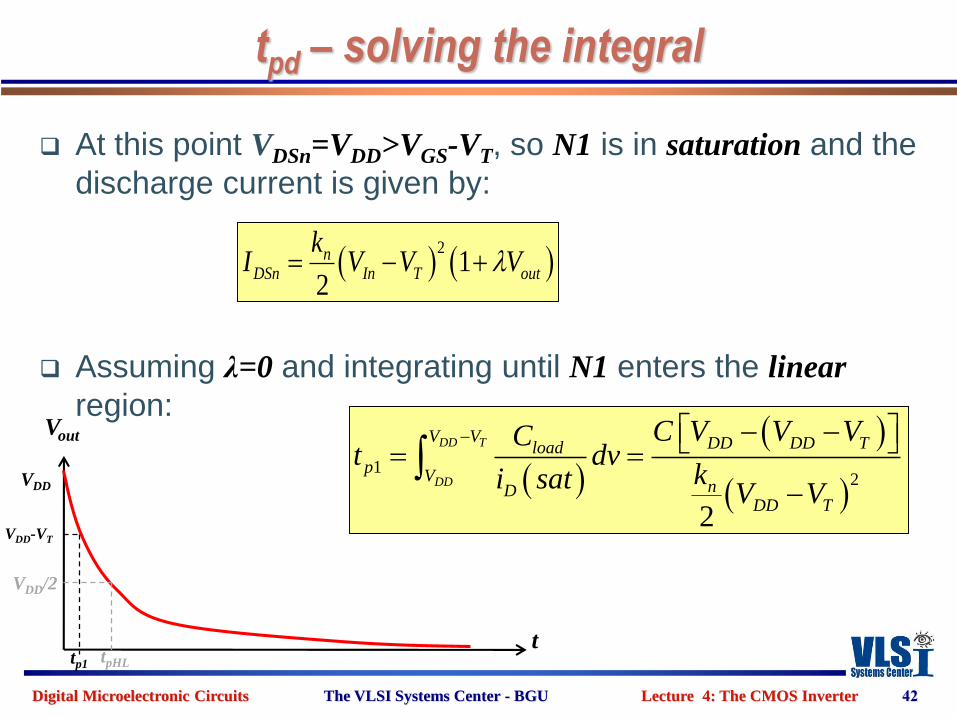
At this point VDSn=VDD>VGS-VT, so N1 is in saturation and the
discharge current is given by:
Assuming λ=0 and integrating until N1 enters the linear
region:
42
2
12
nDSn In T out
kI V V V
1
2
2
DD T
DD
V V DD DD Tloadp
VnD
DD T
C V V VCt dv
ki satV V
t
Vout
VDD
VDD/2
VDD-VT
tp1tpHL
Digital Microelectronic Circuits The VLSI Systems Center - BGU Lecture 4: The CMOS Inverter
tpd – solving the integral
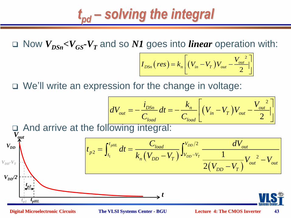
Now VDSn<VGS-VT and so N1 goes into linear operation with:
We’ll write an expression for the change in voltage:
And arrive at the following integral:
43
2
2
outDSn n in T out
VI res k V V V
2
2
DSn n outout in T out
load load
i k VdV dt V V V
C C
1
2
221
2
pHL DD
DD T
t Vload out
pt V V
n DD Tout out
DD T
C dVt dt
k V VV V
V V
t
Vout
VDD
VDD/2
VDD-VT
tp1 tpHL
tp2
Digital Microelectronic Circuits The VLSI Systems Center - BGU Lecture 4: The CMOS Inverter
tpd – solving the integral
Using the equality:
We get:
And putting together the two parts, we get:
For VT=0.2VDD, we get:
44
2
1ln 1
dx
ax x ax
2
3 4lnload DD T
p
n DD
C V Vt
k V
1 2
2 3 41ln
2
load T DD TpHL p p
n DD T DD T DD
C V V Vt t t
k V V V V V
1.6 loadpHL
n DD
Ct
k V
t
Vout
VDD
VDD/2
VDD-VT
tp1 tpHL
tp2
2
221
2
DD
DD TH
Vload out
pV V
n DD Tout out
DD T
C dVt
k V VV V
V V
Digital Microelectronic Circuits The VLSI Systems Center - BGU Lecture 4: The CMOS Inverter
tpd – average currents
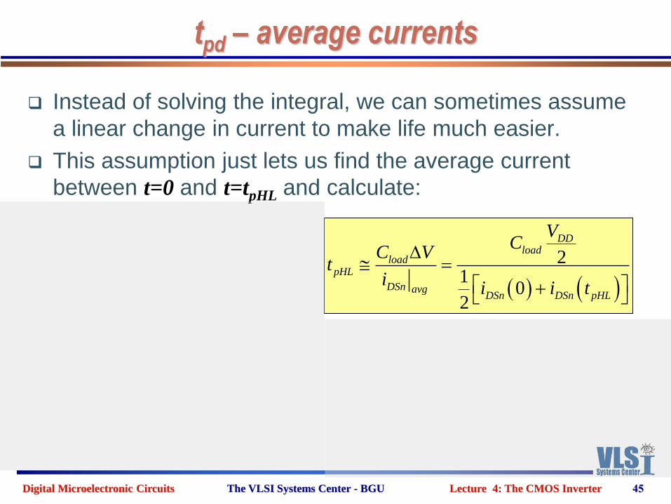
Instead of solving the integral, we can sometimes assume
a linear change in current to make life much easier.
This assumption just lets us find the average current
between t=0 and t=tpHL and calculate:
45
2
10
2
DDload
loadpHL
DSn avgDSn DSn pHL
VC
C Vt
ii i t
Digital Microelectronic Circuits The VLSI Systems Center - BGU Lecture 4: The CMOS Inverter
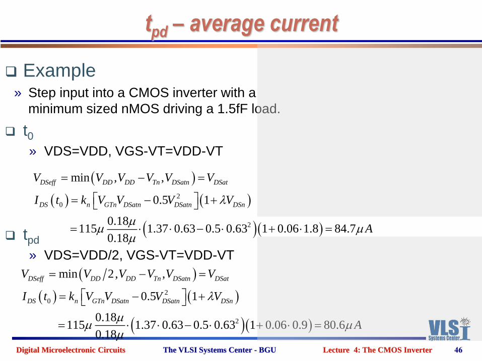
tpd – average current
Example» Step input into a CMOS inverter with a
minimum sized nMOS driving a 1.5fF load.
t0» VDS=VDD, VGS-VT=VDD-VT
tpd
» VDS=VDD/2, VGS-VT=VDD-VT
46
2
0
2
min , ,
0.5 1
0.18115 1.37 0.63 0.5 0.63 1 0.06 1.8 84.7
0.18
DSeff DD DD Tn DSatn DSat
DS n GTn DSatn DSatn DSn
V V V V V V
I t k V V V V
A
2
0
2
min 2, ,
0.5 1
0.18115 1.37 0.63 0.5 0.63 1 0.06 0.9 80.6
0.18
DSeff DD DD Tn DSatn DSat
DS n GTn DSatn DSatn DSn
V V V V V V
I t k V V V V
A
Digital Microelectronic Circuits The VLSI Systems Center - BGU Lecture 4: The CMOS Inverter
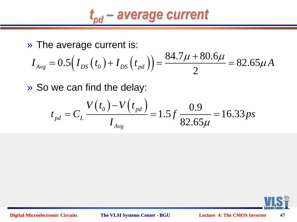
tpd – average current
» The average current is:
» So we can find the delay:
47
0
84.7 80.60.5 82.65
2Avg DS DS pdI I t I t A
0 0.91.5 16.33
82.65
pd
pd L
Avg
V t V tt C f ps
I
Digital Microelectronic Circuits The VLSI Systems Center - BGU Lecture 4: The CMOS Inverter
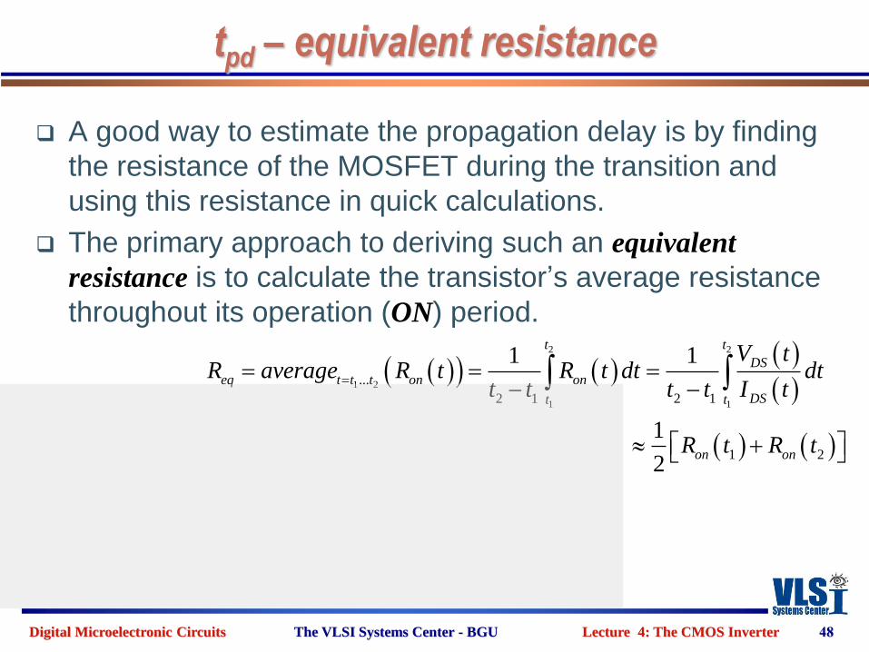
tpd – equivalent resistance
A good way to estimate the propagation delay is by finding
the resistance of the MOSFET during the transition and
using this resistance in quick calculations.
The primary approach to deriving such an equivalent
resistance is to calculate the transistor’s average resistance
throughout its operation (ON) period.
48
2 2
1 2
1 1
...
2 1 2 1
1 2
1 1
1
2
t t
DS
eq t t t on on
DSt t
on on
V tR average R t R t dt dt
t t t t I t
R t R t
Digital Microelectronic Circuits The VLSI Systems Center - BGU Lecture 4: The CMOS Inverter
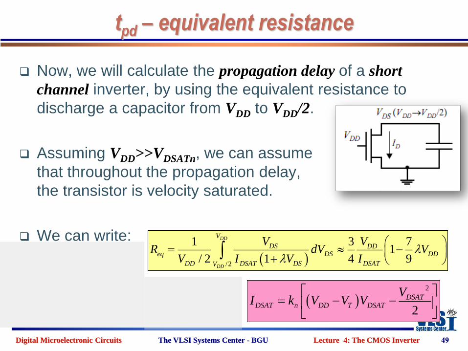
tpd – equivalent resistance
Now, we will calculate the propagation delay of a short
channel inverter, by using the equivalent resistance to
discharge a capacitor from VDD to VDD/2.
Assuming VDD>>VDSATn, we can assume
that throughout the propagation delay,
the transistor is velocity saturated.
We can write:
49
/2
1 3 71
/ 2 1 4 9
DD
DD
V
DS DDeq DS DD
DD DSAT DS DSATV
V VR dV V
V I V I
2
2
DSATDSAT n DD T DSAT
VI k V V V
Digital Microelectronic Circuits The VLSI Systems Center - BGU Lecture 4: The CMOS Inverter
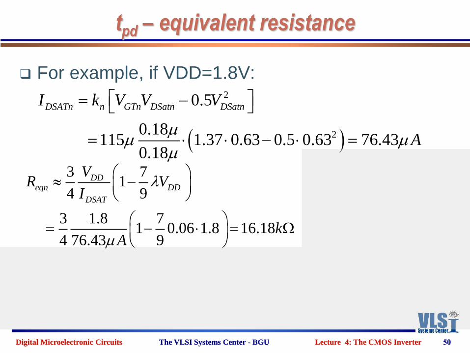
tpd – equivalent resistance
For example, if VDD=1.8V:
50
3 71
4 9
3 1.8 71 0.06 1.8 16.18
4 76.43 9
DDeqn DD
DSAT
VR V
I
kA
2
2
0.5
0.18115 1.37 0.63 0.5 0.63 76.43
0.18
DSATn n GTn DSatn DSatnI k V V V
A
Digital Microelectronic Circuits The VLSI Systems Center - BGU Lecture 4: The CMOS Inverter
tpd – equivalent resistance
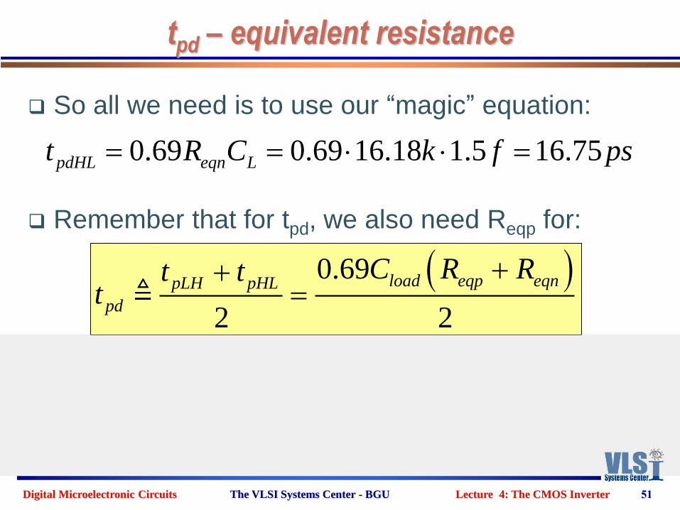
So all we need is to use our “magic” equation:
Remember that for tpd, we also need Reqp for:
51
0.69 0.69 16.18 1.5 16.75pdHL eqn Lt R C k f ps
0.69
2 2
load eqp eqnpLH pHL
pd
C R Rt tt
Digital Microelectronic Circuits The VLSI Systems Center - BGU Lecture 4: The CMOS Inverter
tpd – equivalent resistance
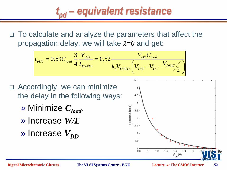
To calculate and analyze the parameters that affect the
propagation delay, we will take λ=0 and get:
Accordingly, we can minimize
the delay in the following ways:
» Minimize Cload.
» Increase W/L
» Increase VDD
52
30.69 0.52
42
DD DD loadpHL load
DSATDSATnn DSATn DD Tn
V V Ct C
VI k V V V

Digital Microelectronic Circuits The VLSI Systems Center - BGU Lecture 4: The CMOS Inverter
Last Lecture
CMOS Inverter
» Intuitive Explanation
» VTC
» VM
» Noise Margins
» Propagation Delay
53
Digital Microelectronic Circuits The VLSI Systems Center - BGU Lecture 4: The CMOS Inverter
Affect of Device Sizing
So we saw that to reduce the propagation delay,
we need to increase the device sizes (W/L).
But how much should we increase them? What are
the tradeoffs?
For this, we will discuss two sizing parameters:
» Beta Ratio (β)
» Upsizing Factor (S)
54
Digital Microelectronic Circuits The VLSI Systems Center - BGU Lecture 4: The CMOS Inverter
What happens when we upsize a transistor?
Effective resistance decreases:
Gate and Drain Capacitance increase:
55
Digital Microelectronic Circuits The VLSI Systems Center - BGU Lecture 4: The CMOS Inverter
Device Sizing - β
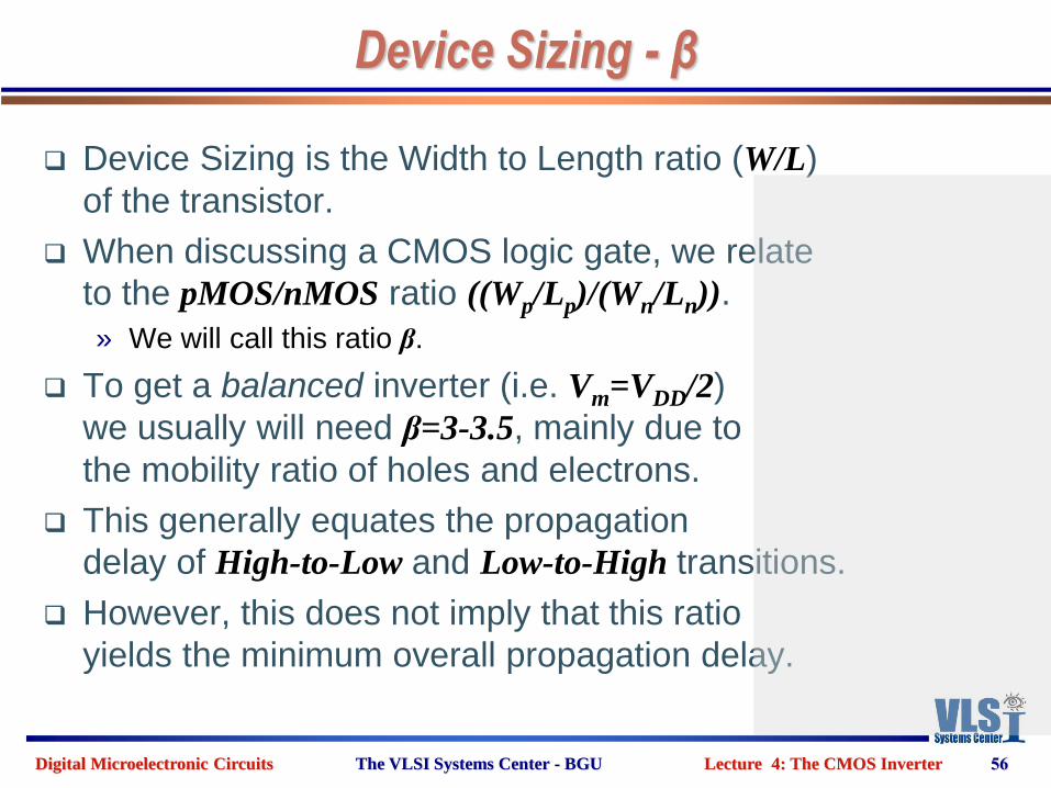
Device Sizing is the Width to Length ratio (W/L)
of the transistor.
When discussing a CMOS logic gate, we relate
to the pMOS/nMOS ratio ((Wp/Lp)/(Wn/Ln)).
» We will call this ratio β.
To get a balanced inverter (i.e. Vm=VDD/2)
we usually will need β=3-3.5, mainly due to
the mobility ratio of holes and electrons.
This generally equates the propagation
delay of High-to-Low and Low-to-High transitions.
However, this does not imply that this ratio
yields the minimum overall propagation delay.
56
Digital Microelectronic Circuits The VLSI Systems Center - BGU Lecture 4: The CMOS Inverter
Device Sizing - β
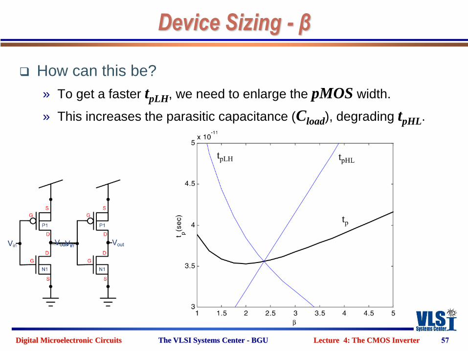
How can this be?
» To get a faster tpLH, we need to enlarge the pMOS width.
» This increases the parasitic capacitance (Cload), degrading tpHL.
57
Digital Microelectronic Circuits The VLSI Systems Center - BGU Lecture 4: The CMOS Inverter
Device Sizing - β
58
Digital Microelectronic Circuits The VLSI Systems Center - BGU Lecture 4: The CMOS Inverter
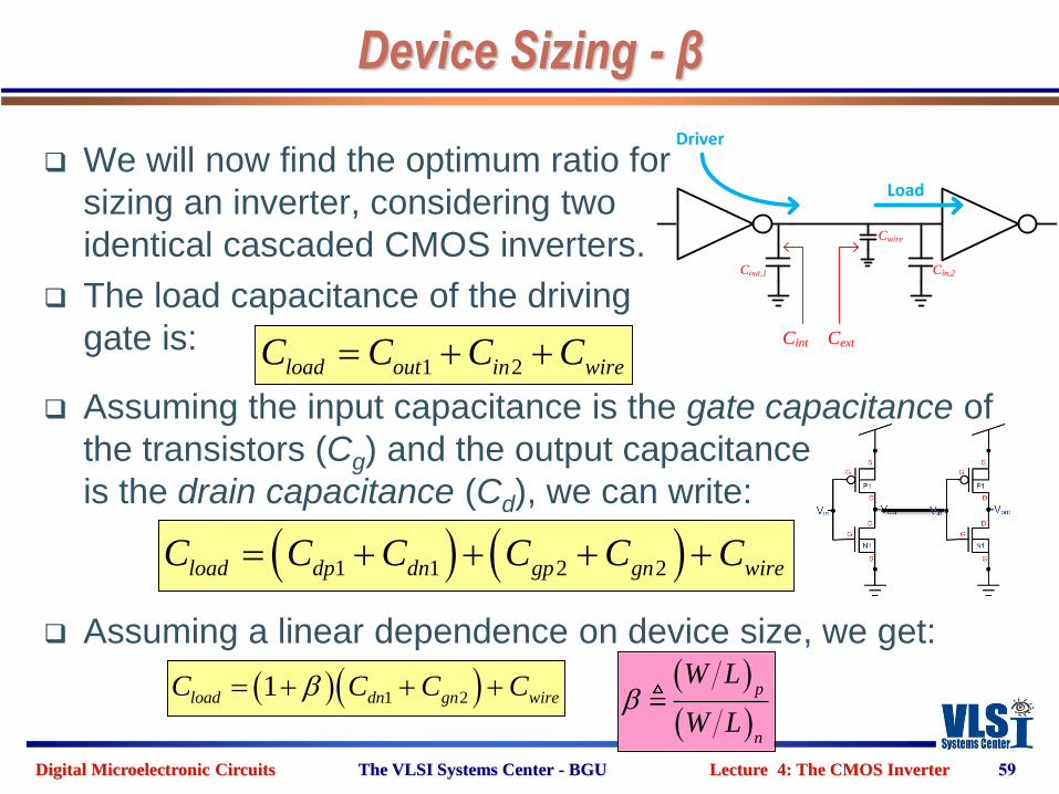
Device Sizing - β
We will now find the optimum ratio for
sizing an inverter, considering two
identical cascaded CMOS inverters.
The load capacitance of the driving
gate is:
Assuming the input capacitance is the gate capacitance of
the transistors (Cg) and the output capacitance
is the drain capacitance (Cd), we can write:
Assuming a linear dependence on device size, we get:
59
1 2load out in wireC C C C
1 21load dn gn wireC C C C
p
n
W L
W L
1 1 2 2load dp dn gp gn wireC C C C C C
Driver
Load
Cint Cext
Cwire
Cin,2Cout,1
Digital Microelectronic Circuits The VLSI Systems Center - BGU Lecture 4: The CMOS Inverter
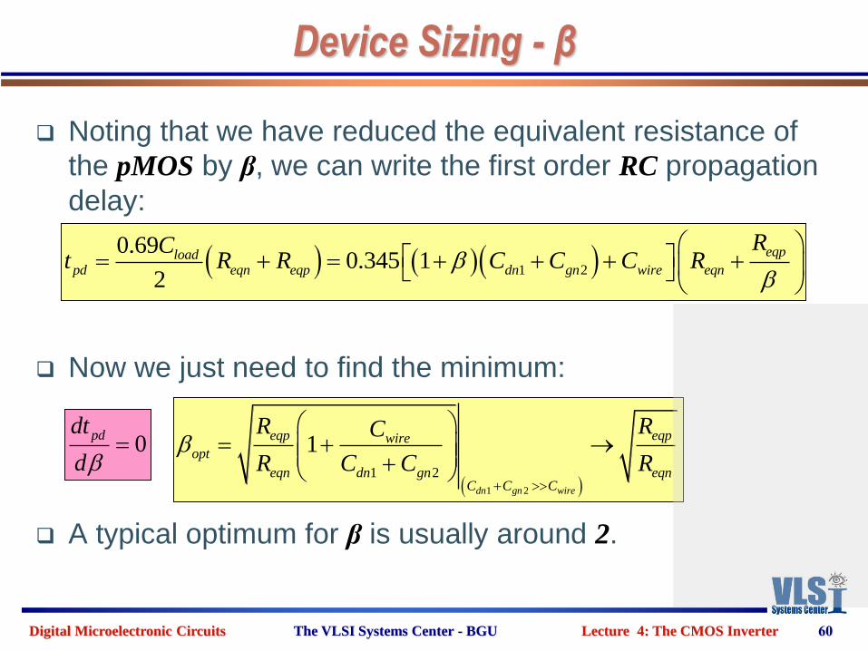
Device Sizing - β
Noting that we have reduced the equivalent resistance of
the pMOS by β, we can write the first order RC propagation
delay:
Now we just need to find the minimum:
A typical optimum for β is usually around 2.
60
1 2
0.690.345 1
2
eqploadpd eqn eqp dn gn wire eqn
RCt R R C C C R
0pddt
d
1 2
1 2
1
dn gn wire
eqp eqpwireopt
eqn dn gn eqnC C C
R RC
R C C R
Digital Microelectronic Circuits The VLSI Systems Center - BGU Lecture 4: The CMOS Inverter
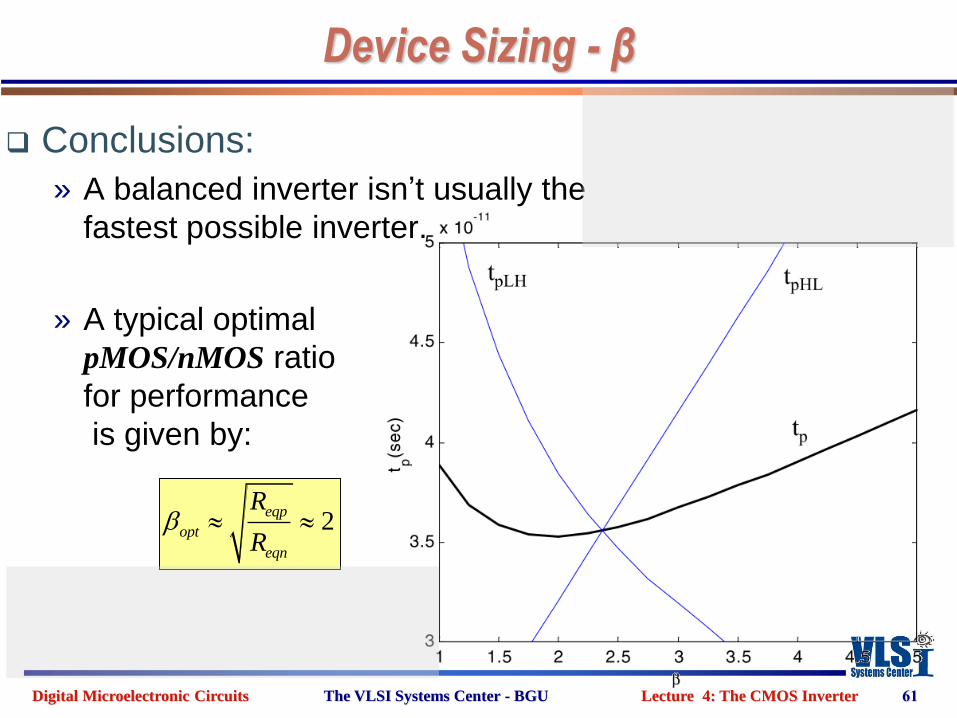
Device Sizing - β
Conclusions:
» A balanced inverter isn’t usually the
fastest possible inverter.
» A typical optimal
pMOS/nMOS ratio
for performance
is given by:
61
2eqp
opt
eqn
R
R
Digital Microelectronic Circuits The VLSI Systems Center - BGU Lecture 4: The CMOS Inverter
Device Sizing - S
We saw how the ratio between the pMOS and
nMOS can be optimized to improve performance.
Now, we will take a balanced inverter and see how
upsizing affects the intrinsic or unloaded delay.
We will start by writing the delay as a function of the
intrinsic capacitance (diffusion and overlap) and the
extrinsic capacitances (fanout and wiring):
62
load int extC C C
int0.69 0.69pd eq load eq extt R C R C C
Digital Microelectronic Circuits The VLSI Systems Center - BGU Lecture 4: The CMOS Inverter
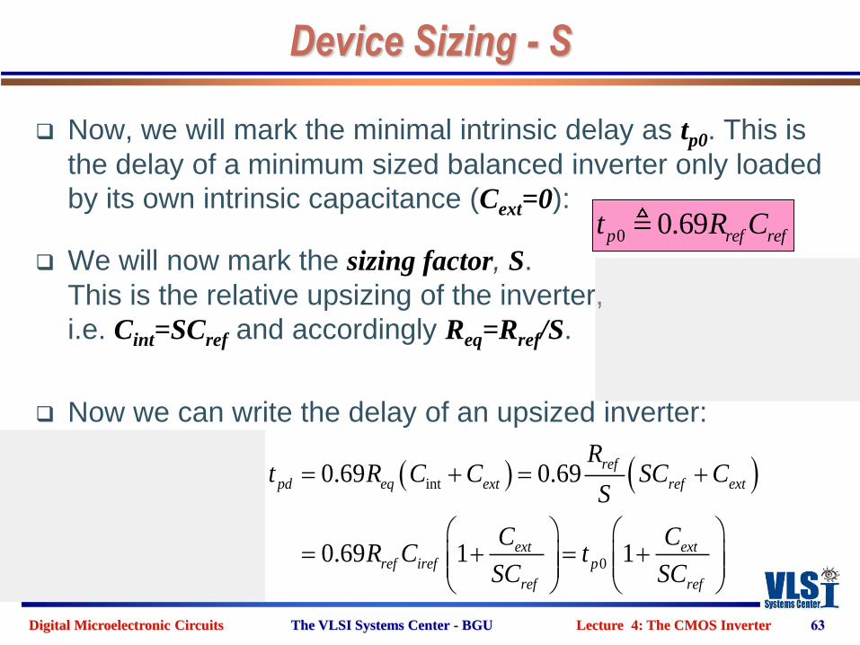
Device Sizing - S
Now, we will mark the minimal intrinsic delay as tp0. This is
the delay of a minimum sized balanced inverter only loaded
by its own intrinsic capacitance (Cext=0):
We will now mark the sizing factor, S.
This is the relative upsizing of the inverter,
i.e. Cint=SCref and accordingly Req=Rref/S.
Now we can write the delay of an upsized inverter:
63
0 0.69p ref reft R C
int
0
0.69 0.69
0.69 1 1
ref
pd eq ext ref ext
ext extref iref p
ref ref
Rt R C C SC C
S
C CR C t
SC SC
Digital Microelectronic Circuits The VLSI Systems Center - BGU Lecture 4: The CMOS Inverter
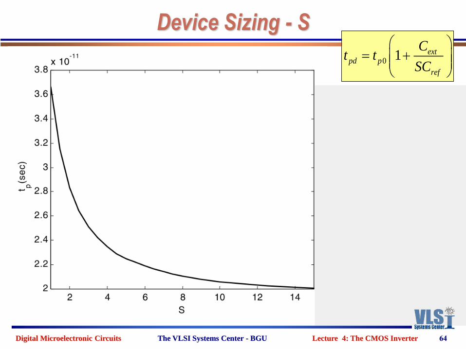
Device Sizing - S
64
0 1 extpd p
ref
Ct t
SC
Digital Microelectronic Circuits The VLSI Systems Center - BGU Lecture 4: The CMOS Inverter
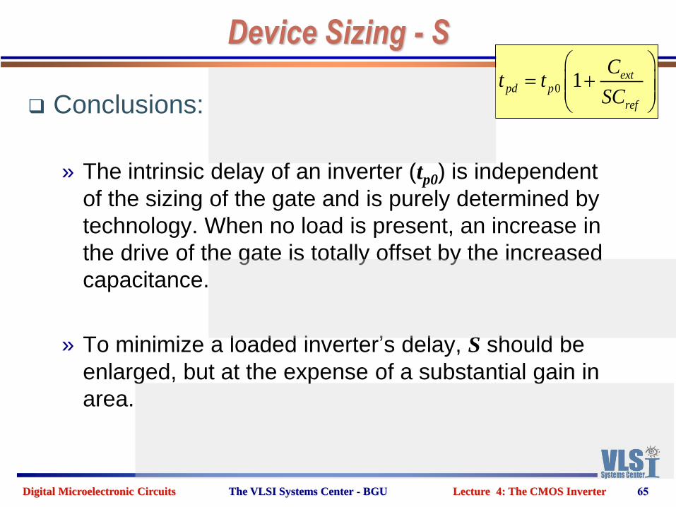
Device Sizing - S
Conclusions:
» The intrinsic delay of an inverter (tp0) is independent
of the sizing of the gate and is purely determined by
technology. When no load is present, an increase in
the drive of the gate is totally offset by the increased
capacitance.
» To minimize a loaded inverter’s delay, S should be
enlarged, but at the expense of a substantial gain in
area.
65
0 1 extpd p
ref
Ct t
SC
Digital Microelectronic Circuits The VLSI Systems Center - BGU Lecture 4: The CMOS Inverter
Summary of Dynamic Parameters
We can calculate tpd in several ways, but the
easiest is to measure the equivalent resistance
during a typical transition.
One of our main techniques to improve the delay is
through transistor sizing, which we discussed in
two fashions:
» Setting the optimal ratio between the PUN/PDN.
» Upsizing the gate to deal with a large output load.
66
Digital Microelectronic Circuits The VLSI Systems Center - BGU Lecture 4: The CMOS Inverter
POWER CONSUMPTION
And now that we fully understand the static and dynamic
operation of the CMOS Inverter, it’s time to take a look at
67
4.44.1 An Intuitive Explanation
4.2 Static Operation
4.3 Dynamic Operation
4.4 Power Consumption
4.5 Summary
Digital Microelectronic Circuits The VLSI Systems Center - BGU Lecture 4: The CMOS Inverter
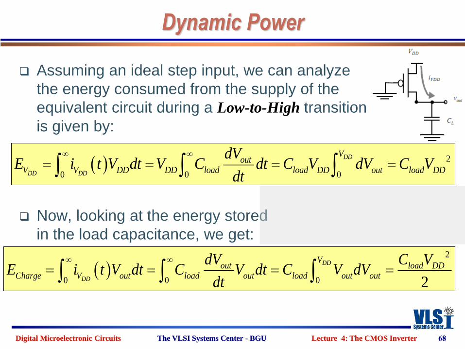
Dynamic Power
Assuming an ideal step input, we can analyze
the energy consumed from the supply of the
equivalent circuit during a Low-to-High transition
is given by:
Now, looking at the energy stored
in the load capacitance, we get:
68
2
0 0 0
DD
DD DD
Vout
V V DD DD load load DD out load DD
dVE i t V dt V C dt C V dV C V
dt
2
0 0 0 2
DD
DD
Vout load DD
Charge V out load out load out out
dV C VE i t V dt C V dt C V dV
dt
Digital Microelectronic Circuits The VLSI Systems Center - BGU Lecture 4: The CMOS Inverter
Dynamic Power
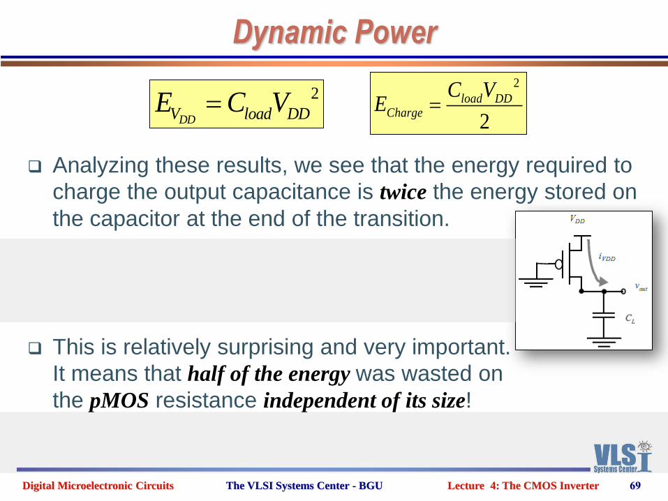
Analyzing these results, we see that the energy required to
charge the output capacitance is twice the energy stored on
the capacitor at the end of the transition.
This is relatively surprising and very important.
It means that half of the energy was wasted on
the pMOS resistance independent of its size!
69
2
DDV load DDE C V2
2
load DDCharge
C VE
Digital Microelectronic Circuits The VLSI Systems Center - BGU Lecture 4: The CMOS Inverter
Dynamic Power
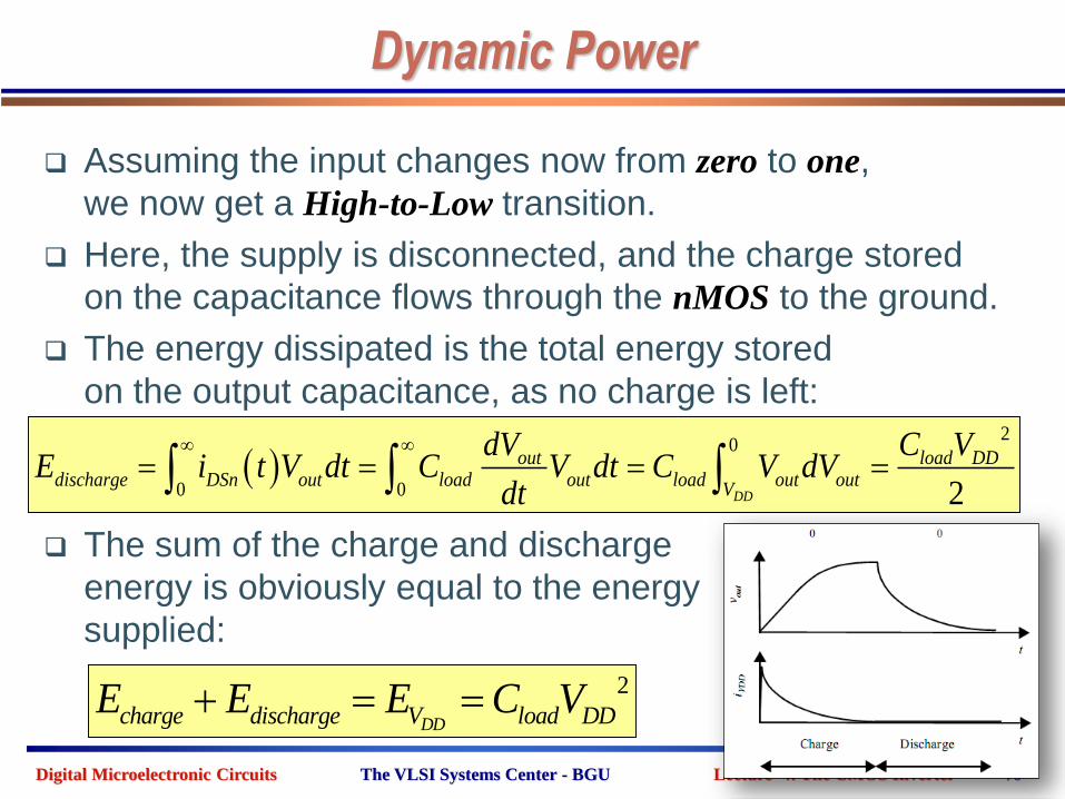
Assuming the input changes now from zero to one,
we now get a High-to-Low transition.
Here, the supply is disconnected, and the charge stored
on the capacitance flows through the nMOS to the ground.
The energy dissipated is the total energy stored
on the output capacitance, as no charge is left:
The sum of the charge and discharge
energy is obviously equal to the energy
supplied:
70
2
0
0 0 2DD
out load DDdischarge DSn out load out load out out
V
dV C VE i t V dt C V dt C V dV
dt
2
DDcharge discharge V load DDE E E C V
Digital Microelectronic Circuits The VLSI Systems Center - BGU Lecture 4: The CMOS Inverter
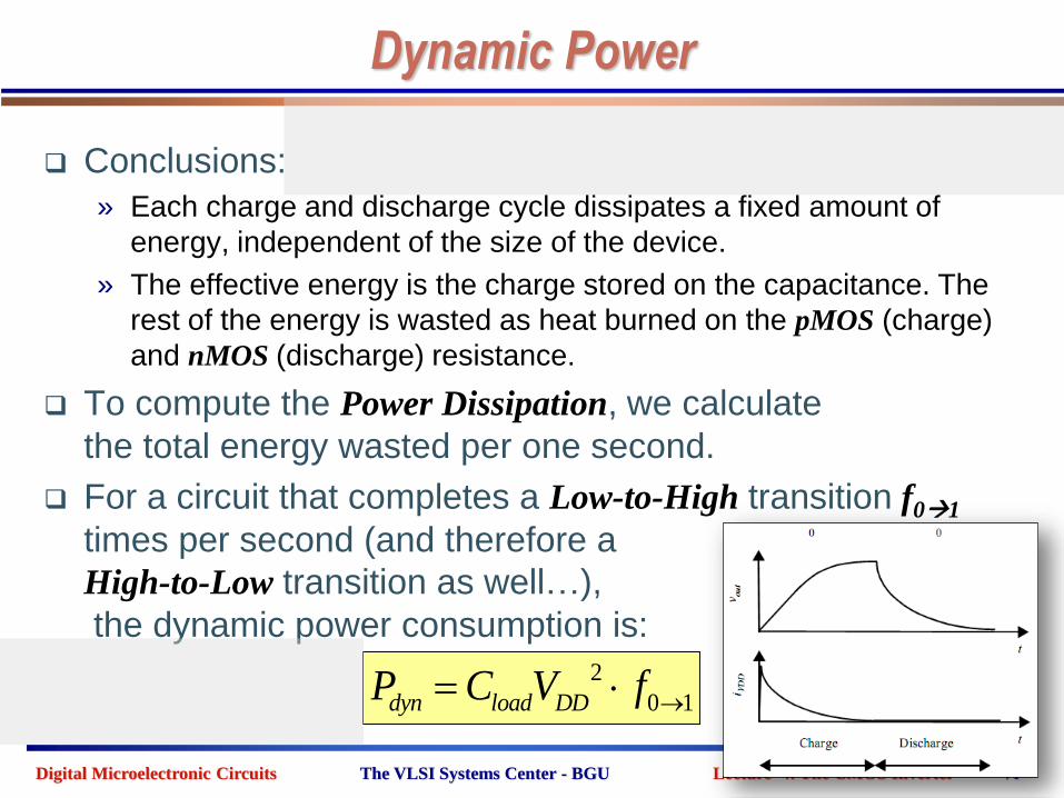
Dynamic Power
Conclusions:
» Each charge and discharge cycle dissipates a fixed amount of
energy, independent of the size of the device.
» The effective energy is the charge stored on the capacitance. The
rest of the energy is wasted as heat burned on the pMOS (charge)
and nMOS (discharge) resistance.
To compute the Power Dissipation, we calculate
the total energy wasted per one second.
For a circuit that completes a Low-to-High transition f01
times per second (and therefore a
High-to-Low transition as well…),
the dynamic power consumption is:
71
2
0 1dyn load DDP C V f
Digital Microelectronic Circuits The VLSI Systems Center - BGU Lecture 4: The CMOS Inverter
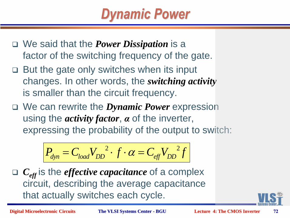
Dynamic Power
We said that the Power Dissipation is a
factor of the switching frequency of the gate.
But the gate only switches when its input
changes. In other words, the switching activity
is smaller than the circuit frequency.
We can rewrite the Dynamic Power expression
using the activity factor, α of the inverter,
expressing the probability of the output to switch:
Ceff is the effective capacitance of a complex
circuit, describing the average capacitance
that actually switches each cycle.
72
2 2
dyn load DD eff DDP C V f C V f
Digital Microelectronic Circuits The VLSI Systems Center - BGU Lecture 4: The CMOS Inverter
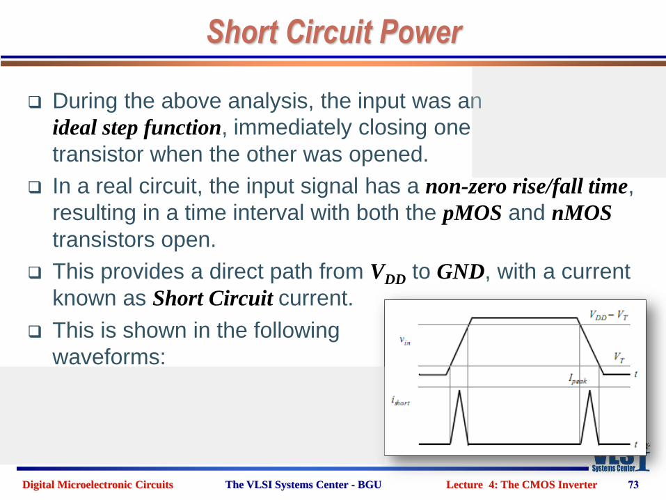
Short Circuit Power
During the above analysis, the input was an
ideal step function, immediately closing one
transistor when the other was opened.
In a real circuit, the input signal has a non-zero rise/fall time,
resulting in a time interval with both the pMOS and nMOS
transistors open.
This provides a direct path from VDD to GND, with a current
known as Short Circuit current.
This is shown in the following
waveforms:
73
Digital Microelectronic Circuits The VLSI Systems Center - BGU Lecture 4: The CMOS Inverter
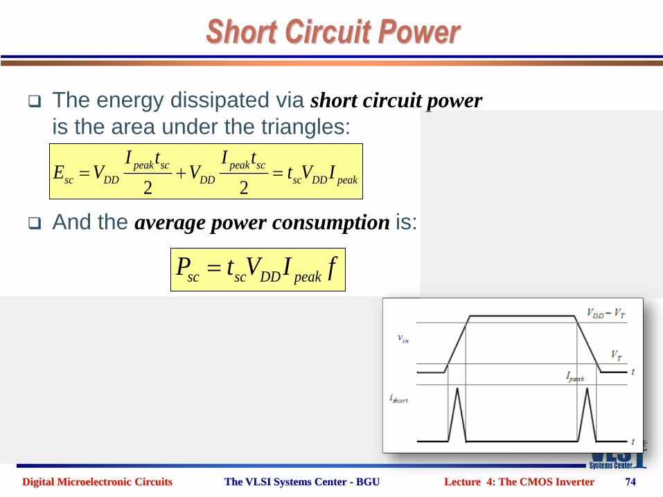
Short Circuit Power
The energy dissipated via short circuit power
is the area under the triangles:
And the average power consumption is:
74
2 2
peak sc peak sc
sc DD DD sc DD peak
I t I tE V V t V I
sc sc DD peakP t V I f
Digital Microelectronic Circuits The VLSI Systems Center - BGU Lecture 4: The CMOS Inverter
Short Circuit Power
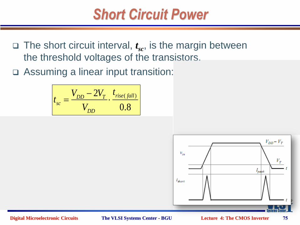
The short circuit interval, tsc, is the margin between
the threshold voltages of the transistors.
Assuming a linear input transition:
75
( )2
0.8
rise fallDD Tsc
DD
tV Vt
V
Digital Microelectronic Circuits The VLSI Systems Center - BGU Lecture 4: The CMOS Inverter
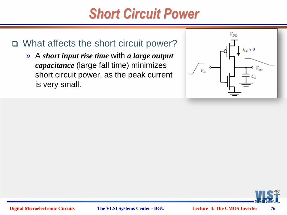
Short Circuit Power
What affects the short circuit power?
» A short input rise time with a large output
capacitance (large fall time) minimizes
short circuit power, as the peak current
is very small.
76
Digital Microelectronic Circuits The VLSI Systems Center - BGU Lecture 4: The CMOS Inverter
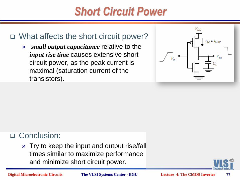
Short Circuit Power
77
What affects the short circuit power?
» small output capacitance relative to the
input rise time causes extensive short
circuit power, as the peak current is
maximal (saturation current of the
transistors).
Conclusion:
» Try to keep the input and output rise/fall
times similar to maximize performance
and minimize short circuit power.
Digital Microelectronic Circuits The VLSI Systems Center - BGU Lecture 4: The CMOS Inverter
Static Power
Ideally, a MOSFET transistor is a perfect switch.
In such a case, a CMOS inverter never has a conducting
path in steady state, resulting
in no static power dissipation.
However, in reality, MOSFET
transistors never completely
turn off.
78
Digital Microelectronic Circuits The VLSI Systems Center - BGU Lecture 4: The CMOS Inverter
Static Power
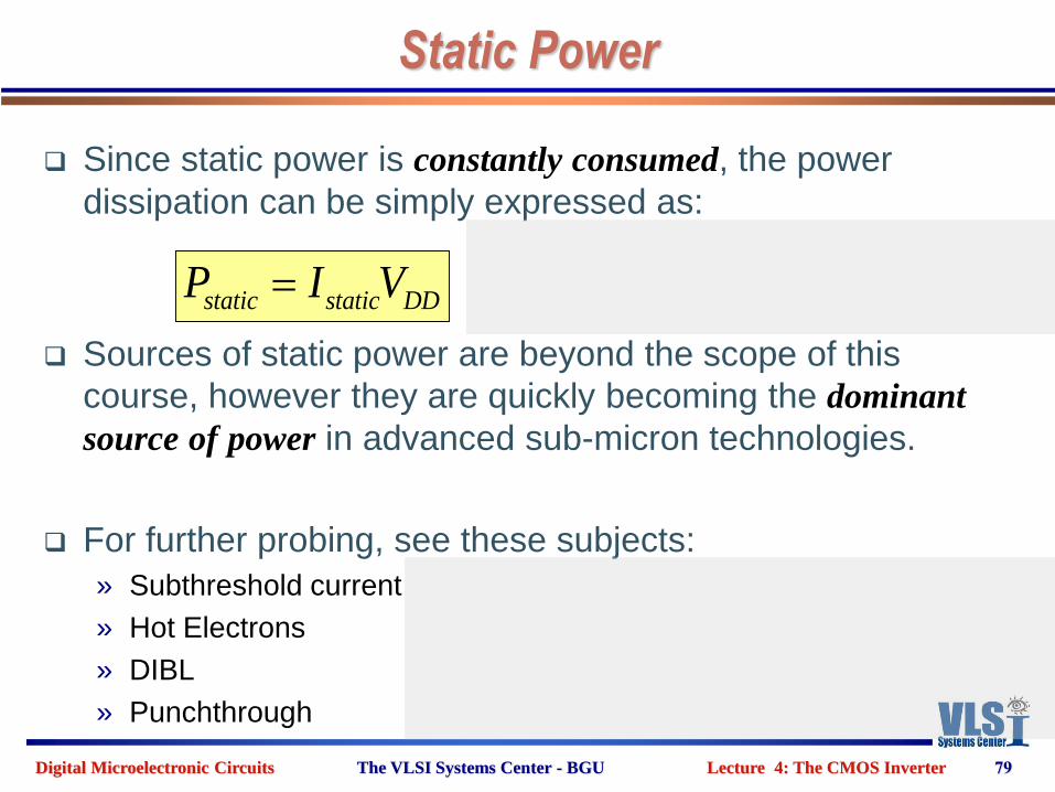
Since static power is constantly consumed, the power
dissipation can be simply expressed as:
Sources of static power are beyond the scope of this
course, however they are quickly becoming the dominant
source of power in advanced sub-micron technologies.
For further probing, see these subjects:
» Subthreshold current
» Hot Electrons
» DIBL
» Punchthrough
79
static static DDP I V
Digital Microelectronic Circuits The VLSI Systems Center - BGU Lecture 4: The CMOS Inverter
Total Power Consumption
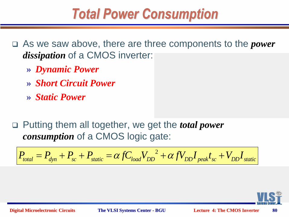
As we saw above, there are three components to the power
dissipation of a CMOS inverter:
» Dynamic Power
» Short Circuit Power
» Static Power
Putting them all together, we get the total power
consumption of a CMOS logic gate:
80
2
total dyn sc static load DD DD peak sc DD staticP P P P fC V fV I t V I
Digital Microelectronic Circuits The VLSI Systems Center - BGU Lecture 4: The CMOS Inverter
Total Power Consumption
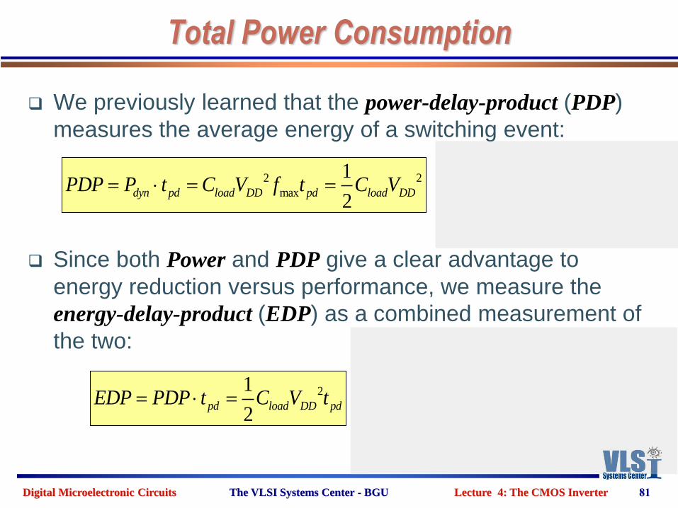
We previously learned that the power-delay-product (PDP)
measures the average energy of a switching event:
Since both Power and PDP give a clear advantage to
energy reduction versus performance, we measure the
energy-delay-product (EDP) as a combined measurement of
the two:
81
2 2
max
1
2dyn pd load DD pd load DDPDP P t C V f t C V
21
2pd load DD pdEDP PDP t C V t
Digital Microelectronic Circuits The VLSI Systems Center - BGU Lecture 4: The CMOS Inverter
SUMMARY
Okay, enough with the inverter. But
before we go on, let’s go over a short
82
4.54.1 An Intuitive Explanation
4.2 Static Operation
4.3 Dynamic Operation
4.4 Power Consumption
4.5 Summary
Digital Microelectronic Circuits The VLSI Systems Center - BGU Lecture 4: The CMOS Inverter
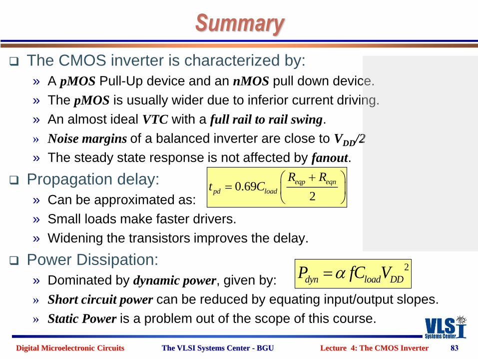
Summary
The CMOS inverter is characterized by:
» A pMOS Pull-Up device and an nMOS pull down device.
» The pMOS is usually wider due to inferior current driving.
» An almost ideal VTC with a full rail to rail swing.
» Noise margins of a balanced inverter are close to VDD/2
» The steady state response is not affected by fanout.
Propagation delay:
» Can be approximated as:
» Small loads make faster drivers.
» Widening the transistors improves the delay.
Power Dissipation:
» Dominated by dynamic power, given by:
» Short circuit power can be reduced by equating input/output slopes.
» Static Power is a problem out of the scope of this course.
83
0.692
eqp eqn
pd load
R Rt C
2
dyn load DDP fC V