Embed Size (px)
Citation preview

Lecture 3RAS 1
Lecture 3
Power Distribution and Clock Design
R. SalehDept. of ECE
University of British [email protected]

Lecture 3RAS 2
Overview of Lecture
• Power distribution in the past was a fairly simple task
• Goal of power distribution system is to deliver the required current across the chip while maintaining the voltage levels necessary for proper operation of logic circuits
• Interconnect effects have created problems of IR drop, Ldi/dt, electromigration.
• Power distribution is now a complex task in deep submicron
• Clock design is also a complex issue in DSM due to RC delay components in the interconnect and power dissipation
• Overall examination of the issues of clock skew and IR drop, and how to manage them using circuit techniques
• Reference:1) “Power Grid and Clock Design”, HJS Textbook, Chapter 11

Lecture 3RAS 3
Design Issues of Power Distribution
• Goal: Get Vdd and Gnd to all gates in the circuit
• Design Challenges:
– How many power and ground pins should we allocate?
– Which layers of metal should be used to route power/ground?
– How wide should be make the wires to minimize voltage drops and reliability problems
– How do we maintain VDD and Gnd within the noise budget?– How do we verify overall power distribution system?

Lecture 3RAS 4
Power Distribution Issues - IR Drop
• Narrowing line widths have increased metal line resistance
• As current flows through power grid, voltage drops occur => IR drops
• Actual voltage supplied to gates is less than Vdd
• Impacts speed and functionality; must be within 10% noise budget
• Need to ensure this is not a problem near the end of the design at tapeout!
n1
n2
n5
n8
n7
n3 n4
n6
Vdd< Vdd
< Vdd

Lecture 3RAS 5
Power Grid Issues – Electromigration (EM)
• As large current flows down narrow wires, metal begins to migrate
• Metal lines break over time due to metal fatigue
• Mean-time to failure is based on average/peak current density
• Need to ensure that current density levels do not exceed limits set by foundry design rules
• Cu is 10X better than Al but we typically see 3X
n1
n2
n5
n8
n7
n3 n4
n6
Current Desity < 10mA/um2

Lecture 3RAS 6
Power Routing Examples
Block A Block B Block A Block B
Single Trunk Multiple Trunks
How do we deliver power to two adjacent blocks to avoid IR and EM?

Lecture 3RAS 7
Simple Routing Examples – cont’d
Block A Block B
Double-Ended Connections Wider Trunks
Block A Block B

Lecture 3RAS 8
Interleaved Power/Ground Routing
Interleaved Vdd/Gnd

Lecture 3RAS 9
Power Grid Architecture
Metal5
Metal4
Via Arrays
Power Grid Using M4/M5

Lecture 3RAS 10

Lecture 3RAS 11
Power Grid Issues – Static IR Drop
• Block placement and global power routing determines IR drop on the chip
• Possible solutions
– Rearrange blocks
– More Vdd pins
– Connect bottom portion of grid to top portion

Lecture 3RAS 12
Power Grid Issues – Static IR Drop
• If we connect bottom portion of grid to top portion, the IR drop is reduced significantly
• However, this is only one part of the problem
• We must also examine electromigration

Lecture 3RAS 13
Case Study – IR and EM Tradeoff
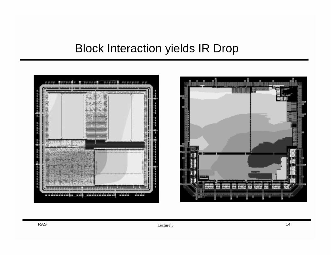
Lecture 3RAS 14
Block Interaction yields IR Drop

Lecture 3RAS 15
Effect of Ldi/dt
• In addition to IR drop, power system inductance is also an issue
• Inductance may be due to power pin or power bump• Overall voltage drop is:
Vdrop = IR + L di
• Simple Example:
– Drop across inductors = 2 x L x di/dt = 2 x 0.2nH x 20mA/100ps = 80mV (problematic if supply is 1.2V)
• Actual power pad or bump may need to support thousands of inverters
dt

Lecture 3RAS 16
IR Drop and Ld/dt are Dynamic Phenomena

Lecture 3RAS 17
On-chip Decoupling Capacitors
• On-chip decaps help to stabilize the power grid voltage
• First line of defense against noise which can extend beyond 10GHz
• Distribute decoupling capacitors (decaps) liberally throughout design
– Capacitors store up charge– Can provide instantaneous source of current for switching– Later, the decap charges back up to prepare for next event
L

Lecture 3RAS 18
Making a Decoupling Cap
• Decaps are basically NMOS transistors. Top plate is polysilicon, bottom-plate is inverted channel, insulator is gate oxide.
• Connect poly to Vdd and source/drain to Vss
• Low-frequency capacitance is roughly COX W L.
• Since these are large capacitance to be used at high frequencies, more accurate representation is needed

Lecture 3RAS 19
Standard Cell Decap Layout
• Standard cells decaps typically have the following layout since we have access to both P and N devices
VDD
VSS

Lecture 3RAS 20
Decap High-Frequency Response
• Channel resistance (affects response time)
• Finite Transit Time (affects capacitance value)
Gate
n+ n+
Gate
n+ n+
- - - - - - - - - - - -
- -
+ + + + + + + + + + + ++ ++ + + ++

Lecture 3RAS 21
Use “Fingers”
• Example:
• With each division, resistance is reduced but so is capacitance.• Question: What is the optimum # of fingers?• Actually, PMOS is worse than NMOS so one option is to use NMOS only

Lecture 3RAS 22
How much Decoupling Cap?
• To estimate required decap value, run SPICE on patch of chip area with power grid, part of logic block, and sprinkle of decaps
• Amount of decap depends on:
– Acceptable ripple on Vdd-Vss (typically 10% noise budget)– Switching activity of logic circuits (usually need 10X switched cap)– Current provided by power grid (di/dt)
– Required frequency response (high frequency operation)– How much decap exists ( non-switching diffusion, gate, wire caps)

Lecture 3RAS 23
Decap Placement
• Empty space is not necessarily the best place to fill with decap since P&R is done with timing and power constraints in mind.
• One method would be to try to shift cells around so that decaps can be placed where they are needed.
• Choose 4 different configurations:– All decap in the center.– All decap in the corners.– Decap distributed evenly.– Decap near cells that violate noise margin.
• Use an equal number of decaps for each configuration. (Equal area penalty.)
• Artificially manipulate the capacitance of each cell until 10%VDD noise is eliminated.
• Best placement scheme is one that requires the least amount of decoupling capacitance.

Lecture 3RAS 24
Noise Violation Configuration

Lecture 3RAS 25
Decap Configurations
Center Corner
Evenly Distributed Noise Violation

Lecture 3RAS 26
Where to place Decaps?
Center Corner
Evenly Distributed Noise Violation

Lecture 3RAS 27
Results
733pFNoise Violations
707pFEvenly Distributed
586pFCorner
684pFCenter
Total DecapStrategy
– Noise Violation Configuration: although requiring the most to eliminate ALL violations, requires the least to eliminate 99% of the violations.
– Should place decaps between charge source and destination– Total switching capacitance in block is 350pF– Ratio between Decoupling Capacitance and Switching Capacitance
seems to be between 1.5-2x.

Lecture 3RAS 28
Designing Power Distribution
• Floorplanner should be aware of IR+Ldi/dt drop and EM problems and design accordingly
– Requires knowledge of current distributions and voltage drop constraints of blocks being placed
• Provide adequate number of VDD and Gnd pins• May need to provide multiple VDD islands for low power
• Route power distribution system according to current demands of the blocks
• Widen wires based on expected current density in branches
• Distribute decoupling capacitors liberally throughout design
• Verify full chip with IR/EM tools

Lecture 3RAS 29
Clock and Flip-flop Design
• Clocks synchronize the operation of sequential logic circuits
• Flip-flops and latches are used to gate signals through combinational logic on the clock edges
• Critical parameters of flip-flops are the setup and hold times• Once we design the basic flops, we must build a clock network
that gets the signal to the flops at roughly the same time
• We will look at clock trees, H-trees and clock grids.
• Overall examination of the issues of clock skew, jitter, power and IR drop, and how to manage them using circuit techniques

Lecture 3RAS 30
Clocked D Flip-flop
• Most widely used FF in IC design for temporary storage of data
• May be edge-triggered (Flip-flop) or level-sensitive (transparent latch)
CK
D Q
Q
data output
D Qn+1
0 01 1
CK
D Q
Q
data output
Flip-flop
Latch

Lecture 3RAS 31
Latch vs. Flip-flop
Latch (level-sensitive, transparent)
When the clock is high it passes In value to Out
When the clock is low, it holds value that In had when the clock fell
Flip-Flop (edge-triggered, non transparent)
On the rising edge of clock (pos-edge trig), it transfers the value of In to Out
It holds the value at all other times.
InIn
OutOut
ClkClk
In
Out Out
In
Latch Flip-Flop
CLK CLK

Lecture 3RAS 32
Clocking Overhead
Latch
Din
Clk
Qout
Tsetup + Tclk-q Td-q
Thold
will workFlip Flop won’t workmay work
Thold
Tsetup
FF and Latches have setup and hold times that must be satisfied:
If Din arrives before setup time and is stable after the hold time, FF will work; if Din arrives after hold time, it will fail; in between, it may or may not work; FF delays the slowest signal by the setup + clk-q delay in the worst case
Latch has small setup and hold times; but it delays the late arriving signals by Td-q
Din
Clk
Qout
Lecture 3RAS 33
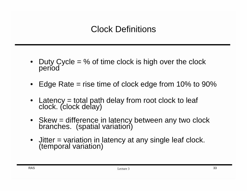
Clock Definitions
• Duty Cycle = % of time clock is high over the clock period
• Edge Rate = rise time of clock edge from 10% to 90%
• Latency = total path delay from root clock to leaf clock. (clock delay)
• Skew = difference in latency between any two clock branches. (spatial variation)
• Jitter = variation in latency at any single leaf clock. (temporal variation)

Lecture 3RAS 34
Clock Design Issues
• Clock cycle depends on a number of factors:
Tcycle = TClk-Q + TLogic + Tsetup+ Tskew + Tjitter
D Q
Clk
D Q
Clk
Logic
N
TLogicTClk-Q TSetup
TSkewTJitter
TJitter

Lecture 3RAS 35
Clock Design Goals
• Meet Design Specs:• Max Skew
• Min/Max Latency (Delay)
• Duty Cycle (Rise/Fall)
• Max Jitter
• Verify Resulting:• Power Consumption
• Area (Gate Count)

Lecture 3RAS 36
Tree and Grid
• Minimal area cost
• Requires clock-tree management
• Use a large superbuffer to drive downstream buffers
• Balancing may be an issue
• Greater area cost
• Easier skew control
• Increased power consumption
• Electromigration risk increased at drivers
• Severely restricts floorplan and routing

Lecture 3RAS 37
Classic H-Tree
• Place clock root at center of chip and distribute as an H-treestructure to all areas of the chip
• Clock is delayed by an equal amount to every section of the chip
• Local skew inside blocks is kept within tolerable limits

Lecture 3RAS 38
Clock Skew Analysis
Flop
Fl opLogic
Late Early
Tcycle = Td +Tsetup + Tclk-q + Tskew
Flop
Late
Fl op
Early
when Tskew + Thold > Tclk-q
Td
Td=0
•CLOCK SKEW causes two problems:
• The cycle time gets longer by the skew
• The part can get the wrong answer
Tclk-q Tsetup
Shows up as a HOLD time violation
Shows up as a SETUP time violation
Fix critical path
Insert buffer
Delay elements

Lecture 3RAS 39
Overhead for a Clock
• CMOS FO4 delay is roughly 425ps/um x Leff
• For 0.13um, FO4 delay � 40 - 50ps
– For a 1GHz clock, this allows < 20 FO4 gate delays/cycle• Clock overhead (including margins for setup/hold)
– 2 FF/Latches cost about 2-3 FO4 delays
– skew costs approximately 2-3 FO4 delays
• Overhead of clock is roughly 4-6 FO4 delays
• 14-16 FO4 delays left to work with for logic • Need to reduce skew and FF cost
CLOCK
Tcycle
Skew Tclk-q TlogicTsetup

Lecture 3RAS 40
Requirements in Flip-Flop Design
• Minimize FF overhead: small clk-q delay, tsetup, thold times
• Minimize power
– flops up to 20% of total power of high-performance systems• High driving capability
– Typical flip-flop load in a 0.18µm CMOS ranges from 50fF to over 100fF, with typical values of 100-150fF in critical paths
• Multiplexed or scan enabled
• Crosstalk insensitivity - dynamic/high impedance nodes are problematic
• Small load on clock to improve performance of clock and reduce power of clock– clocks can consume 40% of total chip power

Lecture 3RAS 41
ITRS Jitter and Skew Trends

Lecture 3RAS 42
Sources of Clock Skew
Main sources:
1. Imbalance between different paths from clock source to FF’s
– interconnect length determines RC delays– capacitive coupling effects cause delay variations
– buffer sizing
– number of loads driven
2. Process variations across die
– interconnect and devices have different statistical variations
Secondary Sources:
1. IR and Ldi/dt in power supply
2. Temperature variations across chip

Lecture 3RAS 43
Contributors to Clock Skew
• From ISSCC 1998
Ref: Geannopoulos98

Lecture 3RAS 44
Contributors to Clock Skew
• Intra-Die PVT Variations• Process
• Transistors (TT, FF, FS, SF, SS)
• Metal (Width, Thickness, etc. ~ RLC)
• Voltage (Power Grid Variations ~ IR-Drop, Ldi/dt)
• Temperature (Correlated to Power Dissipation)
• Tree Branches can’t be Perfectly Balanced• Drivers ~ Wires ~ Flip-Flops

Lecture 3RAS 45
PVT Variability Study
Variation data from IBM and ITRS2005

Lecture 3RAS 46
Spatial Variation Models
Ref: Hashimoto05

Lecture 3RAS 47
PVT Variations
IEEE D&T of Computers Nov-Dec06; Fetzer
P
V
T

Lecture 3RAS 48
Temperature Variations
• Clock delay varies primarily due to variations in VT and mobility, and temp. coeff. of wires

Lecture 3RAS 49
IR Drop Impacts on Clock Skew
Ideal Ideal VddVdd-- Low delayLow delay-- Low skewLow skew
Conservative Conservative VddVdd-- High delayHigh delay-- Low skewLow skew
Actual IR drop impactActual IR drop impact-- delay about 5delay about 5--15% larger15% larger-- skew about 25skew about 25--30% larger30% larger
Delay (latency)Delay (latency)SkewSkew

Lecture 3RAS 50
Reducing the Effects of IR drop and Ldi/dt
• Stagger the firing of clock buffers (bad idea: increases skew)
• Use different power grid tap points for clock buffers (but it makes routing more complicated for automated tools)
• Use smaller buffers (but it degrades edge rates/increases delay)• Make power busses wider (requires area but should do it)
• Use more Vdd/Vss pins; adjust locations of Vdd/Vss pins
• Put in power straps where needed to deliver current
• Place decoupling capacitors wherever there is free space
• Integrate decoupling capacitors into buffer cells These caps act as decoupling
caps when they are not
switching

Lecture 3RAS 51
Power dissipation in Clocks
• Significant power dissipation can occur in clocks in high-performance designs:
• clock switches on every cycle so P= CV2f (i.e., α=1)• clock capacitance can be ~nF range, say 1nF = 1000pF• assuming a power supply of 1.8V, CV = 1800pC of charge• if clock switches every 2ns (500MHz), that’s 0.9A
• for VDD = 1.8V, P=IV=0.9(1.8)=1.6W in the clock circuit alone
• Much of the power (and the skew) occurs in the final drivers due to the sizing up of buffers to drive the flip-flops
• Key to reducing the power is to examine equation CV2f and reduce the terms wherever possible
– VDD is usually given to us; may not want to reduce swing due to coupling noise, etc.
– Look more closely at C and f
Lecture 3RAS 52
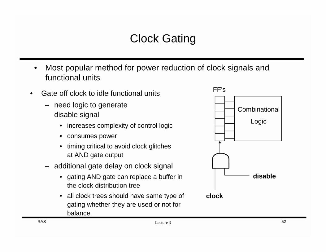
Clock Gating
• Gate off clock to idle functional units
– need logic to generate disable signal
• increases complexity of control logic
• consumes power
• timing critical to avoid clock glitches at AND gate output
– additional gate delay on clock signal• gating AND gate can replace a buffer in
the clock distribution tree
• all clock trees should have same type of gating whether they are used or not for balance
• Most popular method for power reduction of clock signals and functional units
FF’s
Combinational
Logic
disable
clock

Lecture 3RAS 53
Reducing Power in Clocking
• Reduce overall capacitance (shielding vs. spacing)
(a) higher total cap./less area (b) lower cap./ more area
– Tradeoff between the two approaches due to coupling noise
– approach (a) is better for inductive noise; (b) is better for capacitive noise
shield clock shield Signal 1 clock Signal 2

Lecture 3RAS 54
Clock Design Objectives
• Now that we understand the role of the clock and some of the key issues, how do we design it?
– Minimize the clock skew (in presence of IR drop)
– Minimize the clock delay (latency)– Minimize the clock power (and area)
– Maximize noise immunity (due to coupling effects)
– Maximize the clock reliability (signal EM)
• Problems that we will have to deal with
– Routing the clock to all flip-flops on the chip– Driving unbalanced loading, which will not be known until
the chip is nearly completed
– On-chip process/temperature variations

Lecture 3RAS 55
Clock Verification
• Clock verification is more complex in DSM– Must include the effects of RC Interconnect delays in
clock skew analysis along with PVT– Signal integrity (capacitive coupling, inductance)
• spacing vs. shielding– IR drop and Ldi/dt– Signal Electromigration– Clock Jitter is difficult to verify
• time-domain variation of a given clock signal due to random noise, IR drop, temperature, etc.