Embed Size (px)
Citation preview
Embedded Systems Design(630470)
Lecture 4
Memory OrganizationProf. Kasim M. Al-Aubidy
Computer Eng. Dept.
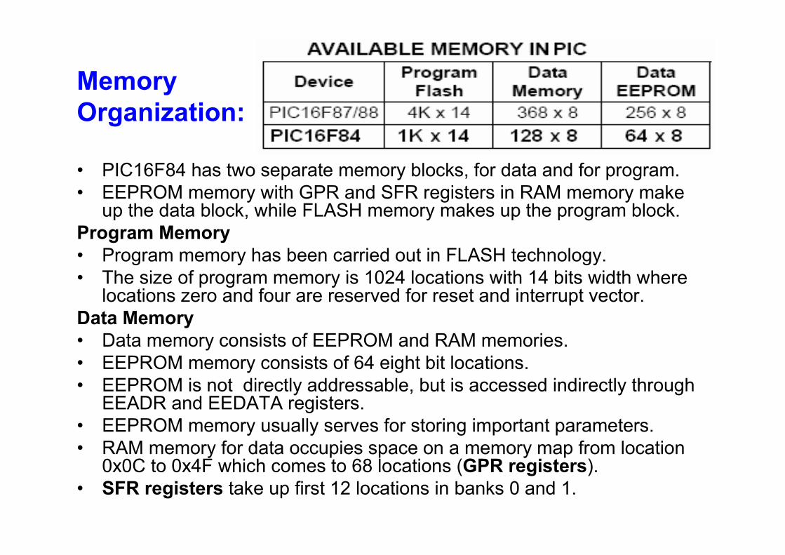
MemoryOrganization:
• PIC16F84 has two separate memory blocks, for data and for program.• EEPROM memory with GPR and SFR registers in RAM memory make
up the data block, while FLASH memory makes up the program block.Program Memory• Program memory has been carried out in FLASH technology.• The size of program memory is 1024 locations with 14 bits width where
locations zero and four are reserved for reset and interrupt vector.Data Memory• Data memory consists of EEPROM and RAM memories.• EEPROM memory consists of 64 eight bit locations.• EEPROM is not directly addressable, but is accessed indirectly through
EEADR and EEDATA registers.• EEPROM memory usually serves for storing important parameters.• RAM memory for data occupies space on a memory map from location
0x0C to 0x4F which comes to 68 locations (GPR registers).• SFR registers take up first 12 locations in banks 0 and 1.
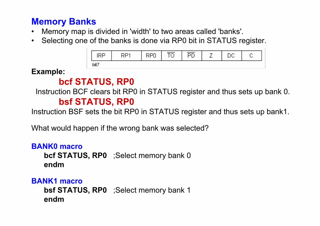
Memory Banks• Memory map is divided in 'width' to two areas called 'banks'.• Selecting one of the banks is done via RP0 bit in STATUS register.
Example:bcf STATUS, RP0
Instruction BCF clears bit RP0 in STATUS register and thus sets up bank 0.bsf STATUS, RP0
Instruction BSF sets the bit RP0 in STATUS register and thus sets up bank1.
What would happen if the wrong bank was selected?
BANK0 macrobcf STATUS, RP0 ;Select memory bank 0endm
BANK1 macrobsf STATUS, RP0 ;Select memory bank 1endm
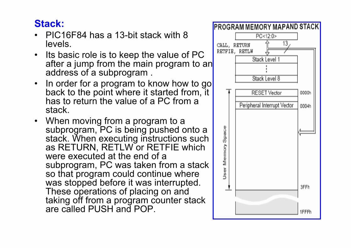
Stack:• PIC16F84 has a 13-bit stack with 8
levels.• Its basic role is to keep the value of PC
after a jump from the main program to anaddress of a subprogram .
• In order for a program to know how to goback to the point where it started from, ithas to return the value of a PC from astack.
• When moving from a program to asubprogram, PC is being pushed onto astack. When executing instructions suchas RETURN, RETLW or RETFIE whichwere executed at the end of asubprogram, PC was taken from a stackso that program could continue wherewas stopped before it was interrupted.These operations of placing on andtaking off from a program counter stackare called PUSH and POP.
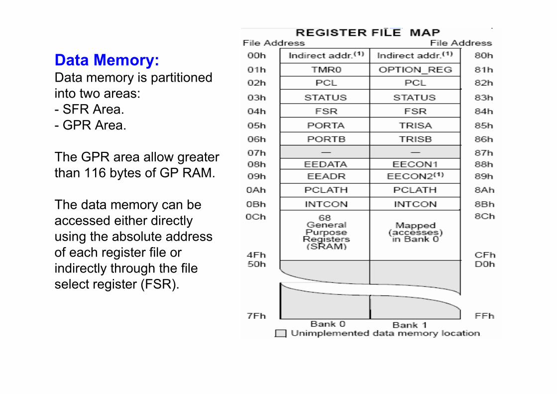
Data Memory:Data memory is partitionedinto two areas:- SFR Area.- GPR Area.
The GPR area allow greaterthan 116 bytes of GP RAM.
The data memory can beaccessed either directlyusing the absolute addressof each register file orindirectly through the fileselect register (FSR).
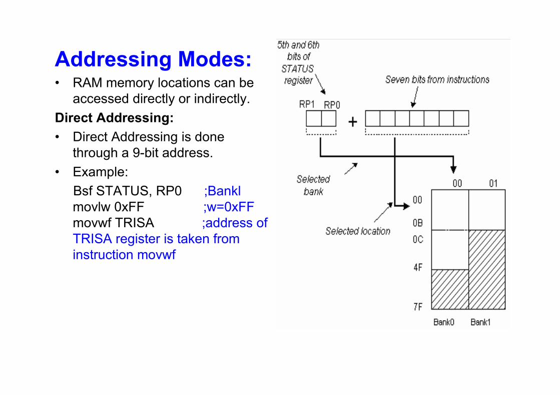
Addressing Modes:• RAM memory locations can be
accessed directly or indirectly.Direct Addressing:• Direct Addressing is done
through a 9-bit address.• Example:
Bsf STATUS, RP0 ;Banklmovlw 0xFF ;w=0xFFmovwf TRISA ;address ofTRISA register is taken frominstruction movwf
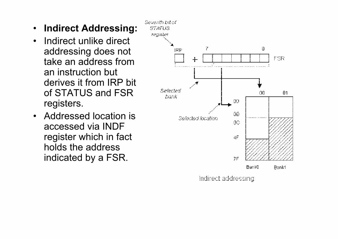
• Indirect Addressing:• Indirect unlike direct
addressing does nottake an address froman instruction butderives it from IRP bitof STATUS and FSRregisters.
• Addressed location isaccessed via INDFregister which in factholds the addressindicated by a FSR.
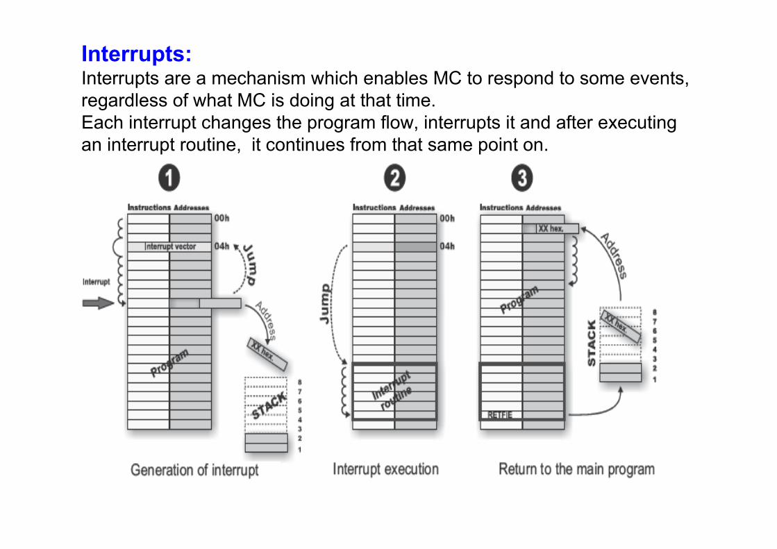
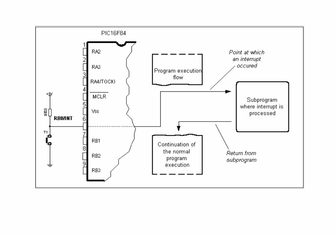
Interrupts:Interrupts are a mechanism which enables MC to respond to some events,regardless of what MC is doing at that time.Each interrupt changes the program flow, interrupts it and after executingan interrupt routine, it continues from that same point on.
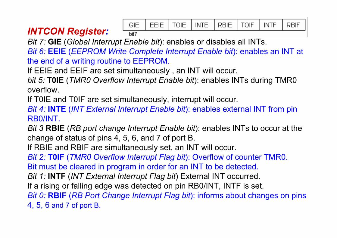
INTCON Register:Bit 7: GIE (Global Interrupt Enable bit): enables or disables all INTs.Bit 6: EEIE (EEPROM Write Complete Interrupt Enable bit): enables an INT atthe end of a writing routine to EEPROM.If EEIE and EEIF are set simultaneously , an INT will occur.bit 5: T0IE (TMR0 Overflow Interrupt Enable bit): enables INTs during TMR0overflow.If T0IE and T0IF are set simultaneously, interrupt will occur.Bit 4: INTE (INT External Interrupt Enable bit): enables external INT from pinRB0/INT.Bit 3 RBIE (RB port change Interrupt Enable bit): enables INTs to occur at thechange of status of pins 4, 5, 6, and 7 of port B.If RBIE and RBIF are simultaneously set, an INT will occur.Bit 2: T0IF (TMR0 Overflow Interrupt Flag bit): Overflow of counter TMR0.Bit must be cleared in program in order for an INT to be detected.Bit 1: INTF (INT External Interrupt Flag bit) External INT occurred.If a rising or falling edge was detected on pin RB0/INT, INTF is set.Bit 0: RBIF (RB Port Change Interrupt Flag bit): informs about changes on pins4, 5, 6 and 7 of port B.
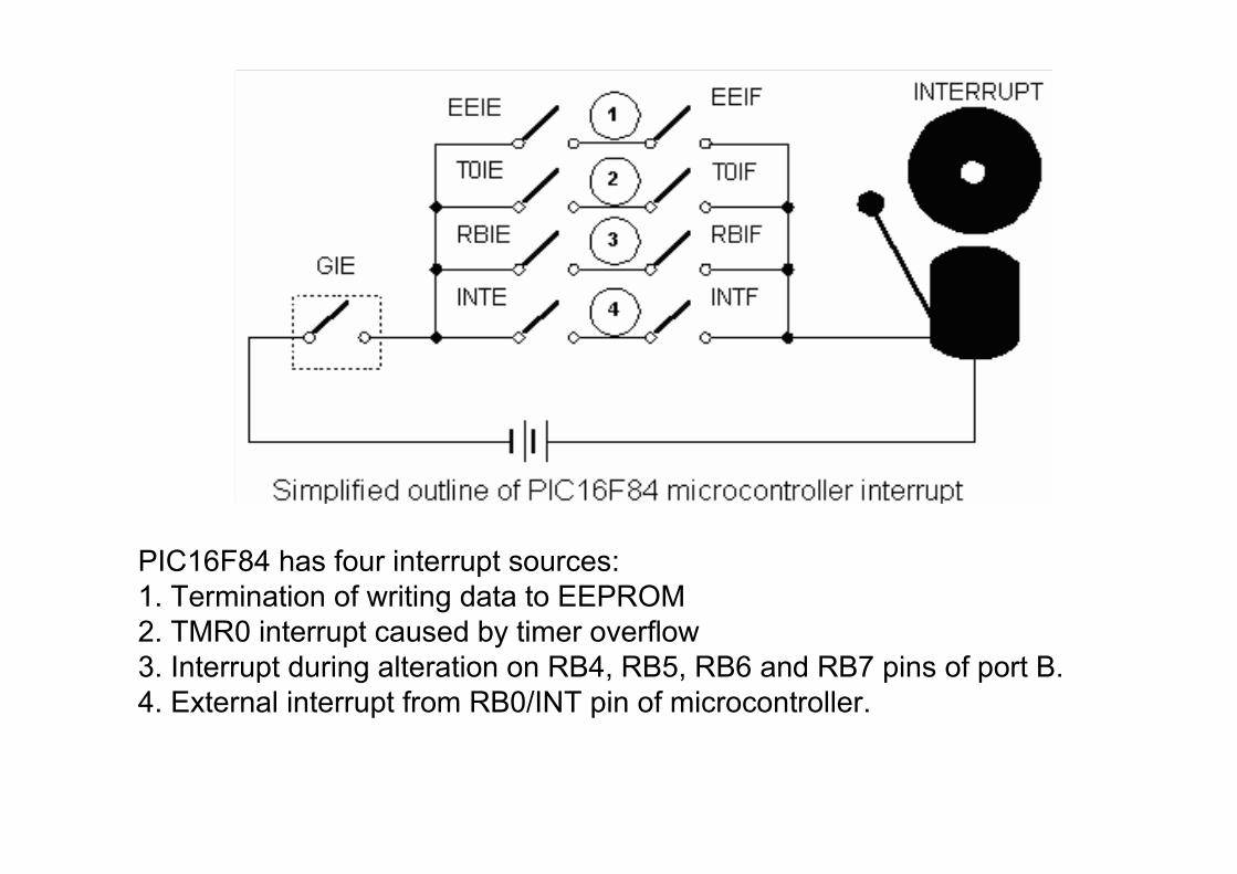
PIC16F84 has four interrupt sources:1. Termination of writing data to EEPROM2. TMR0 interrupt caused by timer overflow3. Interrupt during alteration on RB4, RB5, RB6 and RB7 pins of port B.4. External interrupt from RB0/INT pin of microcontroller.
External interrupt on RB0/INT pin:External interrupt on RB0/INT pin is triggered by rising signal edge (if bitINTEDG=1 in OPTION<6> register), or falling edge (if INTEDG=0).When correct signal appears on INT pin, INTF bit is set in INTCONregister. INTF bit (INTCON<1>) must be cleared in interrupt routine, sothat interrupt wouldn't occur again while going back to the main program.Interrupt can be turned off by resetting INTE control bit (INTCON<4>).
Interrupt during a TMR0 counter overflow:Overflow of TMR0 counter (from FFh to 00h) will set T0IF (INTCON<2>)bit. This is very important interrupt because many real problems can besolved using this interrupt.
Interrupt upon a change on pins 4, 5, 6 and 7 of port B•Change of input signal on PORTB <7:4> sets RBIF (INTCON<0>) bit.•Four pins RB7, RB6, RB5 and RB4 of port B, can trigger an interrupt whichoccurs when status on them changes from logic one to logic zero, or viceversa.•For pins to be sensitive to this change, they must be defined as input. If anyone of them is defined as output, interrupt will not be generated at the changeof status. If they are defined as input, their current state is compared to the oldvalue which was stored at the last reading from port B.
Interrupt upon finishing write-subroutine to EEPROMThis interrupt is of practical nature only. Since writing to one EEPROMlocation takes about 10ms (which is a long time in the notion of a MC), itdoesn't pay off to a MC to wait for writing to end.Thus interrupt mechanism is added which allows the MC to continueexecuting the main program, while writing in EEPROM is being done in thebackground.When writing is completed, interrupt informs the MC that writing has ended.EEIF bit, through which this informing is done, is found in EECON1 register.Occurrence of an interrupt can be disabled by resetting the EEIE bit.
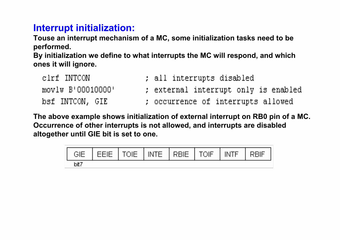
Interrupt initialization:Touse an interrupt mechanism of a MC, some initialization tasks need to beperformed.By initialization we define to what interrupts the MC will respond, and whichones it will ignore.
The above example shows initialization of external interrupt on RB0 pin of a MC.Occurrence of other interrupts is not allowed, and interrupts are disabledaltogether until GIE bit is set to one.


![[XLS] · Web view005B PC Memory - 4MB 005C PC Memory - 6MB 005D PC Memory - 8MB 005E PC Memory - 10MB 005F PC Memory - 12MB 005G PC Memory - 14MB 005H PC Memory - 16MB 005I PC Memory](https://img.pdfslide.net/doc/110x75/5ab13df97f8b9ac66c8c4031/xls-view005b-pc-memory-4mb-005c-pc-memory-6mb-005d-pc-memory-8mb-005e-pc.jpg)