Embed Size (px)
Citation preview
1
Logic Design I (17.341)
Fall 2011
Lecture Outline
Class # 09
November 14, 2011
Dohn Bowden

2
Today’s Lecture
• Administrative
• Main Logic Topic
• Homework

3
CourseAdmin

4
Administrative
• Admin for tonight …
– Syllabus Review

5
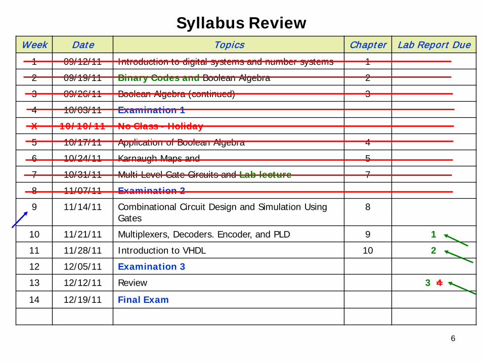
Syllabus
• Syllabus
– Lab due dates have been modified as follows …
• Lab #1 Due next week … 11/21/11• Lab #2 Due 11/28/11• Lab #3 Due 12/12/11• Lab #4 Deleted
– For planning purposes … Exam #3 is on 11/28/11 … in three weeks!
6
Syllabus ReviewWeek Date Topics Chapter Lab Report Due
1 09/12/11 Introduction to digital systems and number systems 1
2 09/19/11 Binary Codes and Boolean Algebra 2
3 09/26/11 Boolean Algebra (continued) 3
4 10/03/11 Examination 1
X 10/10/11 No Class - Holiday
5 10/17/11 Application of Boolean Algebra 4
6 10/24/11 Karnaugh Maps and 5
7 10/31/11 Multi-Level Gate Circuits and Lab lecture 7
8 11/07/11 Examination 2
9 11/14/11 Combinational Circuit Design and Simulation Using Gates
8
10 11/21/11 Multiplexers, Decoders. Encoder, and PLD 9 1
11 11/28/11 Introduction to VHDL 10 2
12 12/05/11 Examination 3
13 12/12/11 Review 3 4
14 12/19/11 Final Exam

Exam #2
• Take home exam … DUE TONIGHT … November 14, 2011
7

8
Questions?
9
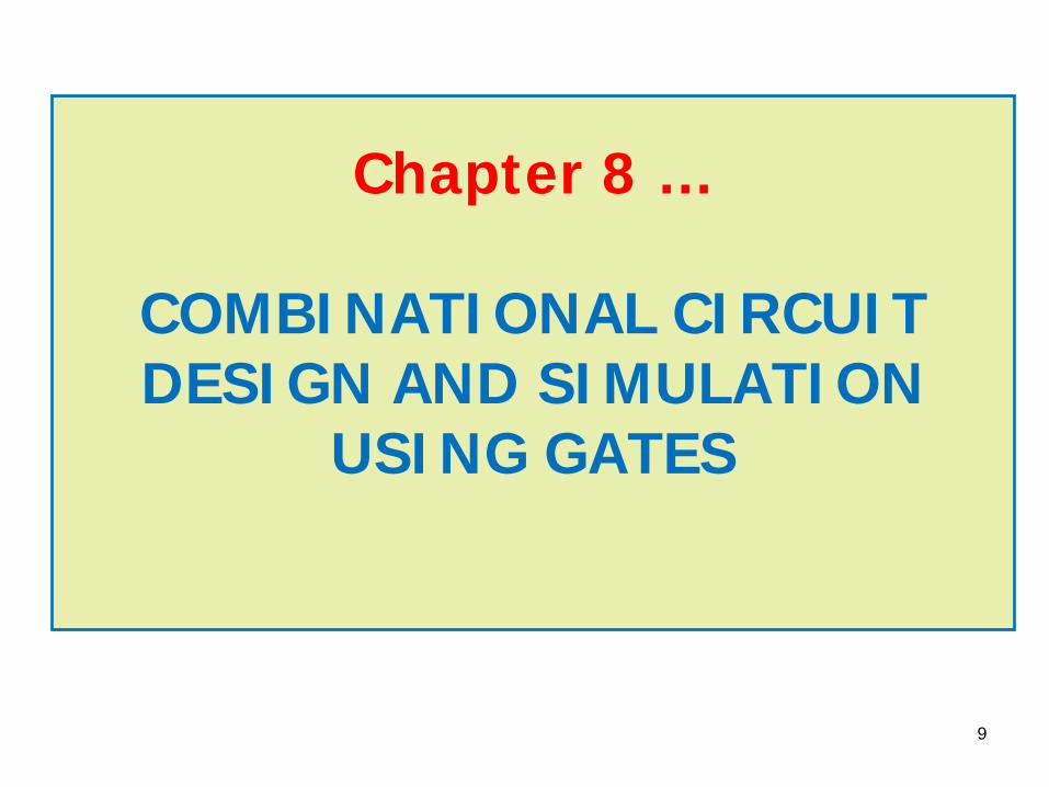
Chapter 8 …
COMBINATIONAL CIRCUIT DESIGN AND SIMULATION
USING GATES

10
Objectives
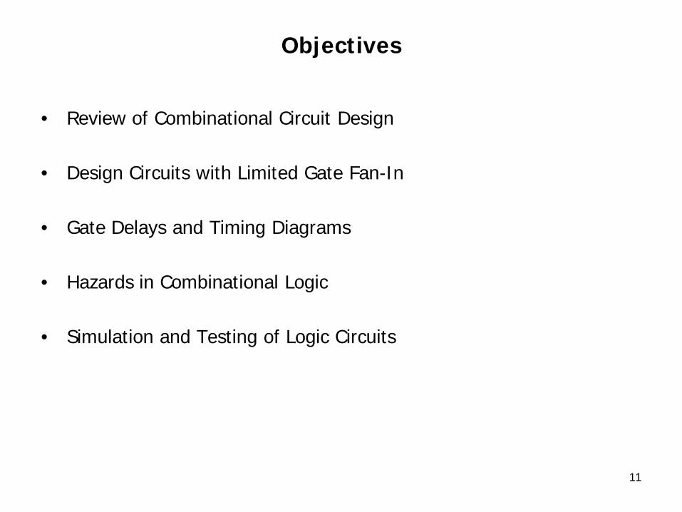
Objectives
• Review of Combinational Circuit Design
• Design Circuits with Limited Gate Fan-In
• Gate Delays and Timing Diagrams
• Hazards in Combinational Logic
• Simulation and Testing of Logic Circuits
11
12
Review of CombinationalCircuit Design
Review of Combinational Circuit Design
• The first step in the design of a combinational switching circuit is usually to set up a truth table …
– Which specifies the output(s) as a function of the input variables
• The next step is to derive simplified algebraic expressions for the output functions using K-maps … or … a similar procedure
• In some cases … it may be desirable to go directly from the problem statement to algebraic equations … without writing down a truth table
• The resulting equations are simplified algebraically
13
Review of Combinational Circuit Design
• The simplified algebraic expressions are then manipulated into the proper form …
– Depending on the type of gates to be used in realizing the circuit
• The number of levels in a gate circuit is equal to the maximum number of gates through which a signal must pass when going between the input and output terminals
• The minimum sum of products … or … product of sums … leads directly to a minimum two-level gate circuit
14
Review of Combinational Circuit Design
• In some applications it is desirable to increase the number of levels by …
– Factoring … or …
– Multiplying out
• Factoring … or … Multiplying out may lead to a reduction in the number of gates or gate inputs
15
Review of Combinational Circuit Design
• When a circuit has two or more outputs … common terms in the output functions can be used to reduce the total number of gates or gate inputs
• If each function is minimized separately … this does not always lead to a minimum multiple-output circuit
• For a two-level circuit … K-maps of the output functions can be used to find the common terms
• All of the terms in the minimum multiple-output circuit will not necessarily be prime implicants of the individual functions
16
Review of Combinational Circuit Design
• When designing circuits with three or more levels … looking for common terms on the K-maps may be of little value
• The designer will often minimize the functions separately and …
– Then use ingenuity to factor the expressions in such a way to create common terms
17
Review of Combinational Circuit Design
• Minimum two-level AND-OR … NAND-NAND … OR-NAND … and … NOR-OR circuits can be realized using …
– The minimum sum of products as a starting point
• Minimum two-level OR-AND … NOR-NOR … AND-NOR … and NAND-AND circuits can be realized using the minimum product of sums as a starting point
18
Review of Combinational Circuit Design
• Design of multi-level, multiple-output NAND- gate circuits is most easily accomplished by …
– First designing a circuit of AND and OR gates.
– If this circuit has an OR gate at each output and is arranged so that an AND gate … or OR gate output is never connected to the same type of gate ….
• A direct conversion to a NAND- gate circuit is possible
19
Review of Combinational Circuit Design
• A direct conversion to a NAND- gate circuit is accomplished by …
– Replacing all of the AND and OR gates with NAND gates … and … then inverting any literals which appear as inputs to the first, third, fifth, . . . levels (output gates are the first level)
• If the AND-OR circuit has an AND gate … or OR gate output connected to the same type of gate … then …
– Extra inverters must be added in the conversion process
• Similarly, design
20
Review of Combinational Circuit Design
• Design of multi-level … multiple-output NOR- gate circuits is most easily accomplished by …
– First designing a circuit of AND and OR gates
– The best starting point is usually the minimum sum-of-products expressions for the complements of the output functions
21
Review of Combinational Circuit Design
• After factoring these expressions to the desired form …
– They are then complemented to get expressions for the output functions … and the corresponding circuit of AND and OR gates is drawn
– If this circuit has an AND gate at each output … and an AND gate … or OR gate output is never connected to the same type of gate …
• A direct conversion to a NOR- gate circuit is possible
– Otherwise … extra inverters must be added in the conversion process
22

23
Design of Circuits with Limited Gate Fan-In
Design of Circuits with Limited Gate Fan-In
• Fan-in …
– The maximum number of inputs on each gate
• In practical logic design problems …
– The maximum number of inputs on each gate is limited
24
Design of Circuits with Limited Gate Fan-In
• If a two-level realization of a circuit requires more gate inputs than allowed …
– Factoring the logic expression to obtain a multi-level realization is necessary
25

26
Example …
Example … More gate inputs than allowed
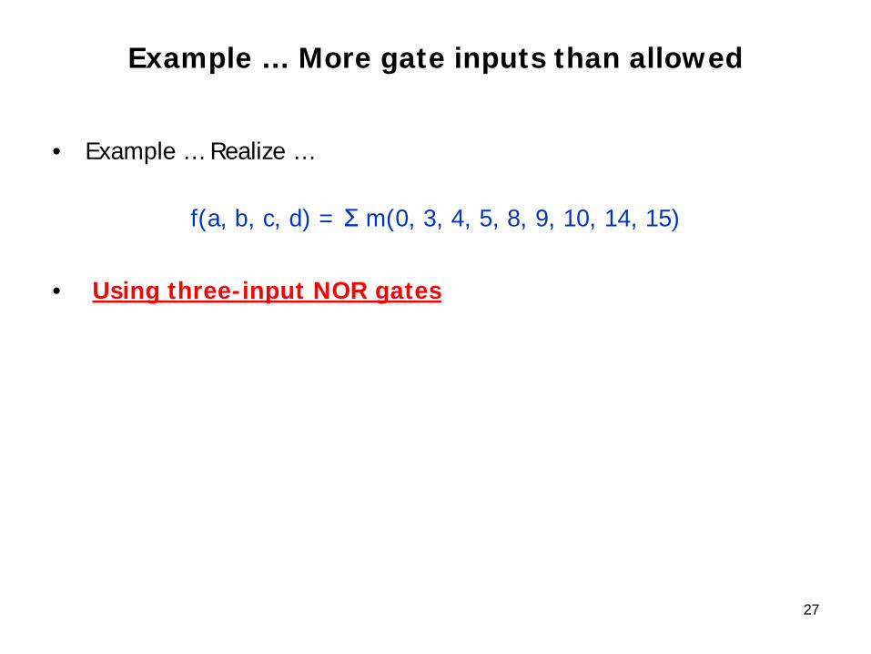
• Example … Realize …
f(a, b, c, d) = Ʃ m(0, 3, 4, 5, 8, 9, 10, 14, 15)
• Using three-input NOR gates
27
Example … More gate inputs than allowed
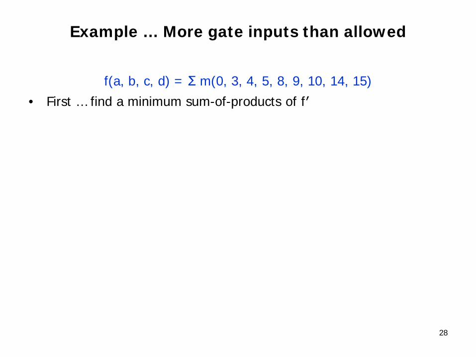
f(a, b, c, d) = Ʃ m(0, 3, 4, 5, 8, 9, 10, 14, 15)
• First … find a minimum sum-of-products of f′
28
Example … More gate inputs than allowed
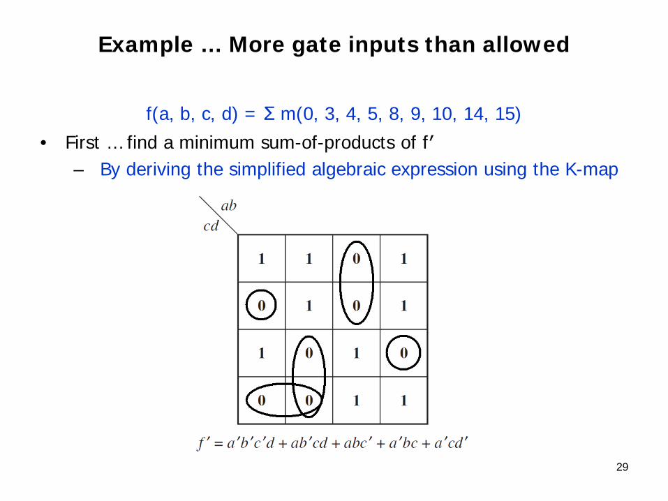
f(a, b, c, d) = Ʃ m(0, 3, 4, 5, 8, 9, 10, 14, 15)
• First … find a minimum sum-of-products of f′– By deriving the simplified algebraic expression using the K-map
29
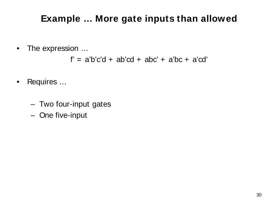
Example … More gate inputs than allowed
• The expression …f’ = a’b’c’d + ab’cd + abc’ + a’bc + a’cd’
• Requires …
– Two four-input gates– One five-input
30
Example … More gate inputs than allowed
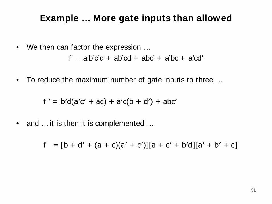
• We then can factor the expression …f’ = a’b’c’d + ab’cd + abc’ + a’bc + a’cd’
• To reduce the maximum number of gate inputs to three …
f ′ = b′d(a′c′ + ac) + a′c(b + d′) + abc′
• and … it is then it is complemented …
f = [b + d′ + (a + c)(a′ + c′)][a + c′ + b′d][a′ + b′ + c]
31
Example … More gate inputs than allowed
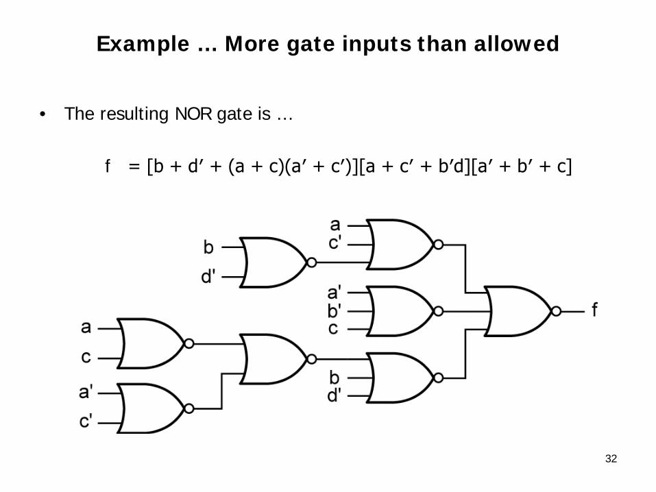
• The resulting NOR gate is …
f = [b + d′ + (a + c)(a′ + c′)][a + c′ + b′d][a′ + b′ + c]
32
33
Multiple Output Circuits …
Design of Multiple-Output Circuits
• Previous techniques for designing two-level … multiple-output circuits …
– Are not very effective for designing multiple-output circuits with more than two levels
• When two-level expressions had common terms …
– Most of these common terms would be lost when the expressions were factored
34
Design of Multiple-Output Circuits
• When designing multiple-output circuits … with more than two levels …
– It is usually best to minimize each function separately
• The resulting two-level expressions must then be factored to increase the number of levels
– Factoring should be done in such a way as to introduce common terms wherever possible
35

36
Example …
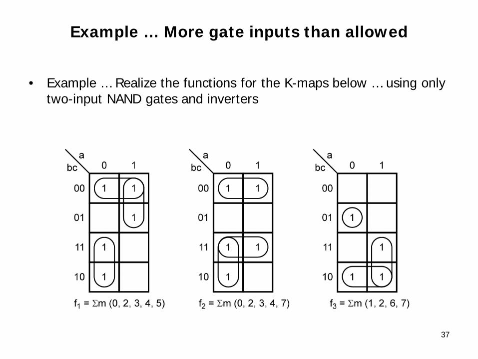
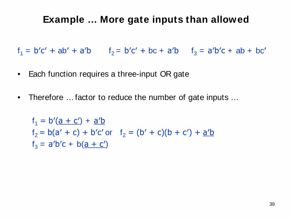
Example … More gate inputs than allowed
• Example … Realize the functions for the K-maps below … using only two-input NAND gates and inverters
37
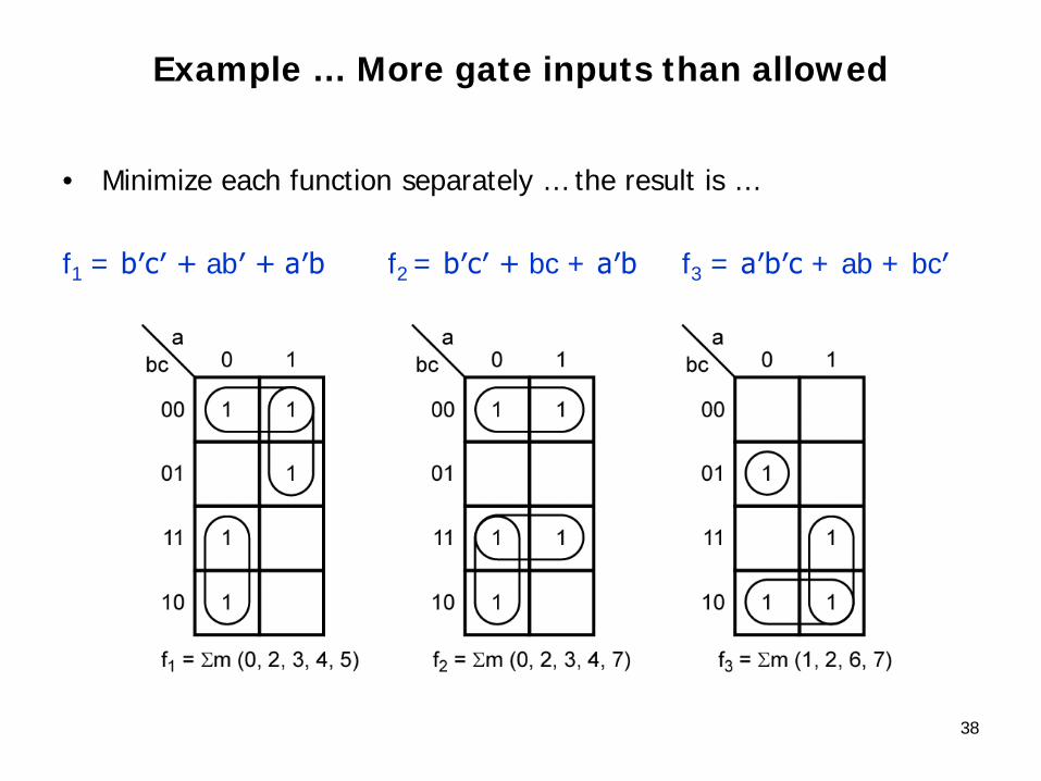
Example … More gate inputs than allowed
• Minimize each function separately … the result is …
f1 = b′c′ + ab′ + a′b f2 = b′c′ + bc + a′b f3 = a′b′c + ab + bc′
38
Example … More gate inputs than allowed
f1 = b′c′ + ab′ + a′b f2 = b′c′ + bc + a′b f3 = a′b′c + ab + bc′
• Each function requires a three-input OR gate
• Therefore … factor to reduce the number of gate inputs …
f1 = b′(a + c′) + a′bf2 = b(a′ + c) + b′c′ or f2 = (b′ + c)(b + c′) + a′bf3 = a′b′c + b(a + c′)
39
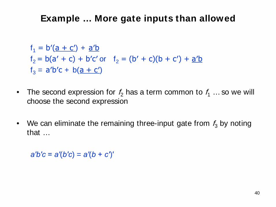
Example … More gate inputs than allowed
f1 = b′(a + c′) + a′bf2 = b(a′ + c) + b′c′ or f2 = (b′ + c)(b + c′) + a′bf3 = a′b′c + b(a + c′)
• The second expression for f2 has a term common to f1 … so we will choose the second expression
• We can eliminate the remaining three-input gate from f3 by noting that …
a′b′c = a′(b′c) = a′(b + c′)′
40
Example … More gate inputs than allowed
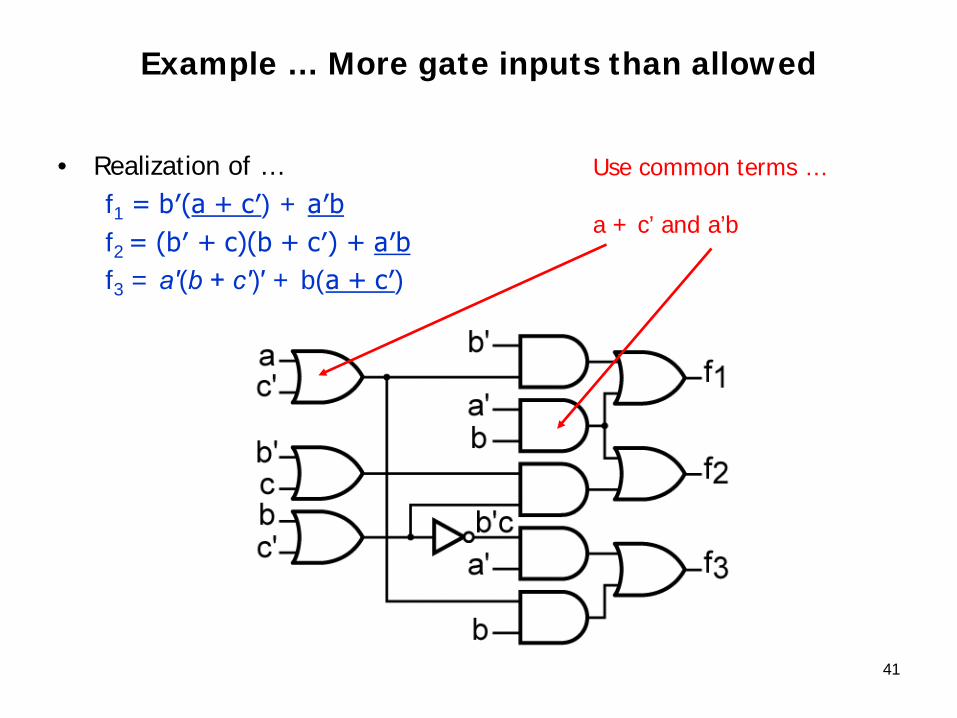
• Realization of … f1 = b′(a + c′) + a′bf2 = (b′ + c)(b + c′) + a′bf3 = a′(b + c′)′ + b(a + c′)
41
Use common terms …
a + c’ and a’b
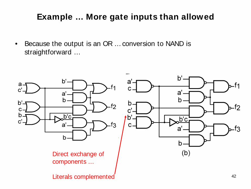
Example … More gate inputs than allowed
• Because the output is an OR … conversion to NAND is straightforward …
42
Direct exchange of components …
Literals complemented
43
Gate Delays and Timing Diagrams

44
Gate Delays …
Gate Delays
• When the input to a logic gate is changed …
– The output will not change instantaneously
• The transistors or other switching elements within the gate take a finite time to react to a change in input … so that …
– The change in the gate output is delayed with respect to the input change
45
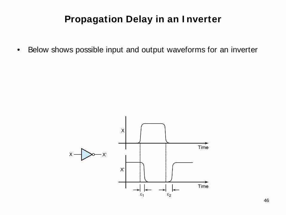
Propagation Delay in an Inverter
• Below shows possible input and output waveforms for an inverter
46
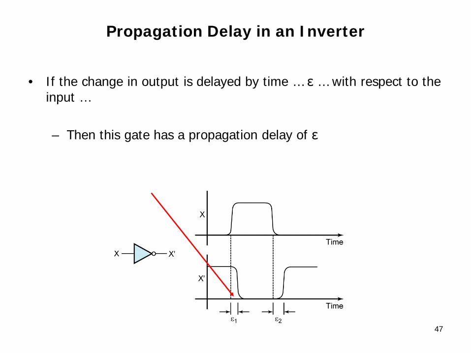
Propagation Delay in an Inverter
• If the change in output is delayed by time … ε … with respect to the input …
– Then this gate has a propagation delay of ε
47
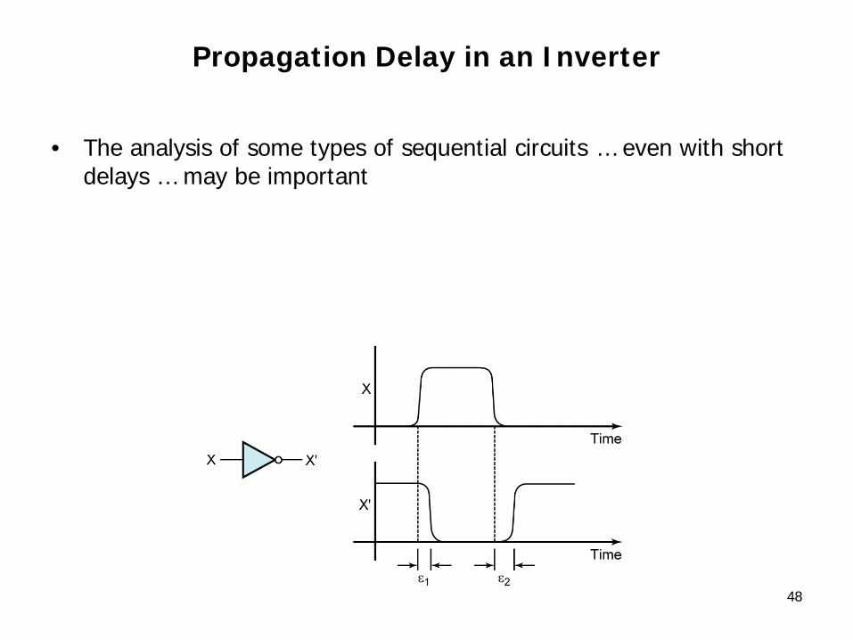
Propagation Delay in an Inverter
• The analysis of some types of sequential circuits … even with short delays … may be important
48
49
Timing Diagrams …
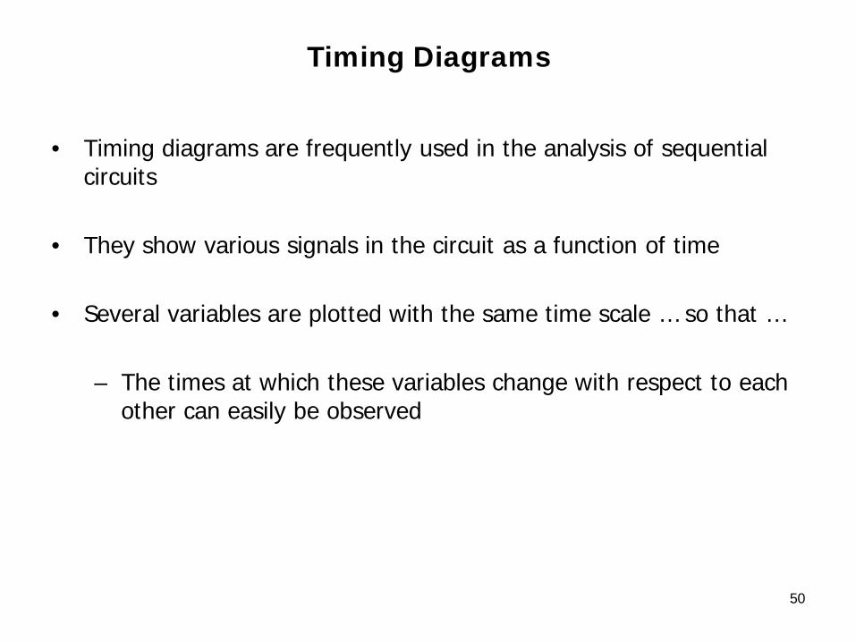
Timing Diagrams
• Timing diagrams are frequently used in the analysis of sequential circuits
• They show various signals in the circuit as a function of time
• Several variables are plotted with the same time scale … so that …
– The times at which these variables change with respect to each other can easily be observed
50
Timing Diagrams
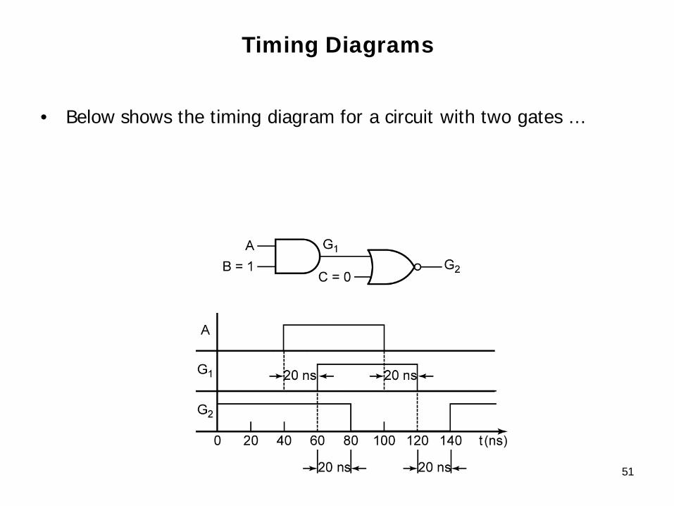
• Below shows the timing diagram for a circuit with two gates …
51
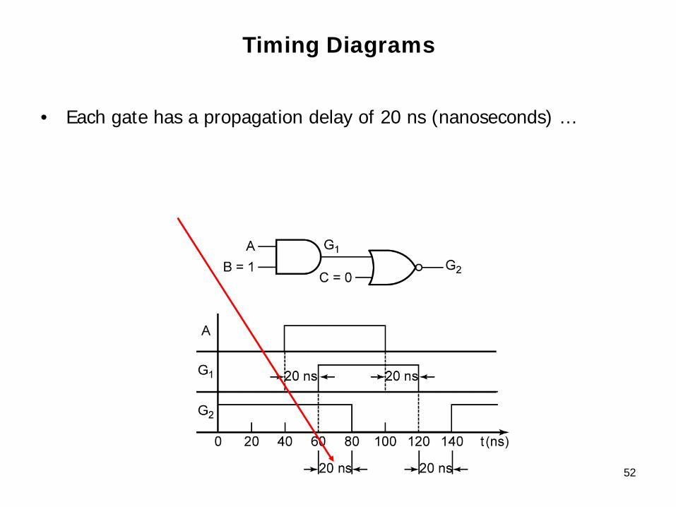
Timing Diagrams
• Each gate has a propagation delay of 20 ns (nanoseconds) …
52
Timing Diagrams
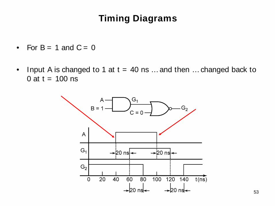
• For B = 1 and C = 0
• Input A is changed to 1 at t = 40 ns … and then … changed back to 0 at t = 100 ns
53
Timing Diagrams
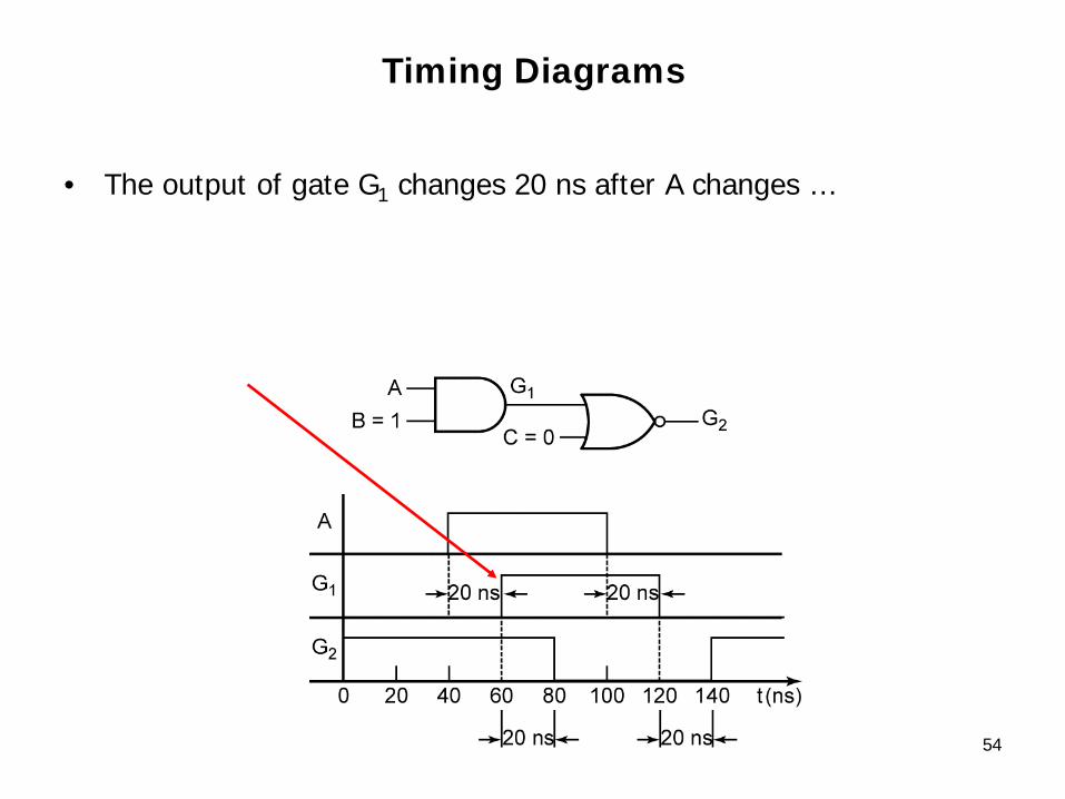
• The output of gate G1 changes 20 ns after A changes …
54
Timing Diagrams
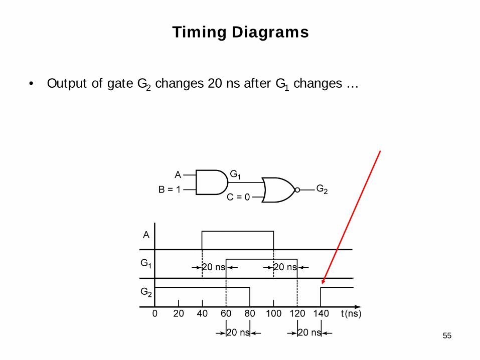
• Output of gate G2 changes 20 ns after G1 changes …
55

56
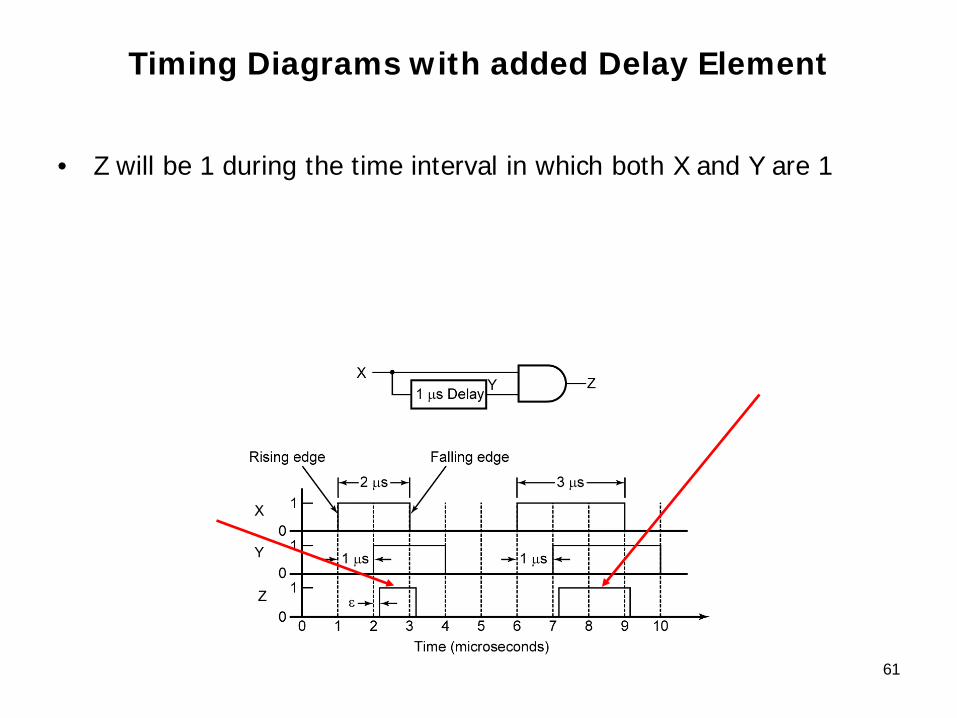
Timing Diagrams with added Delay Element …
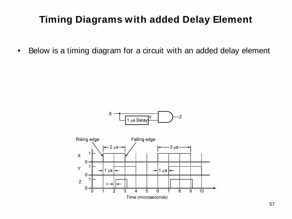
Timing Diagrams with added Delay Element
• Below is a timing diagram for a circuit with an added delay element
57
Timing Diagrams with added Delay Element
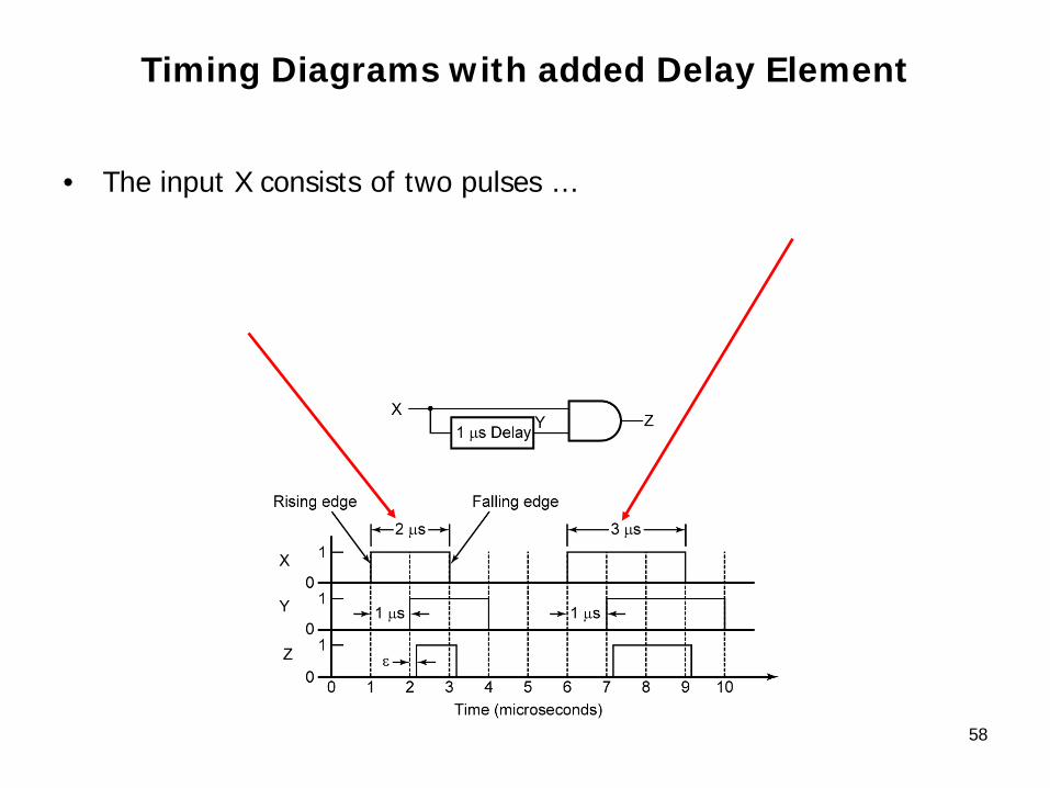
• The input X consists of two pulses …
58
Timing Diagrams with added Delay Element
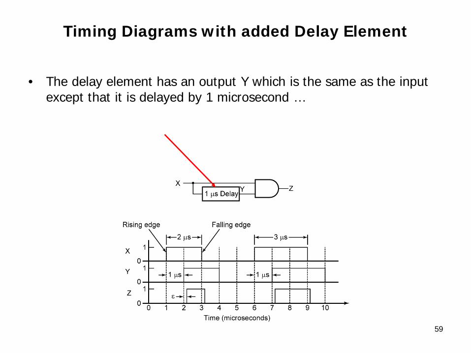
• The delay element has an output Y which is the same as the input except that it is delayed by 1 microsecond …
59
Timing Diagrams with added Delay Element
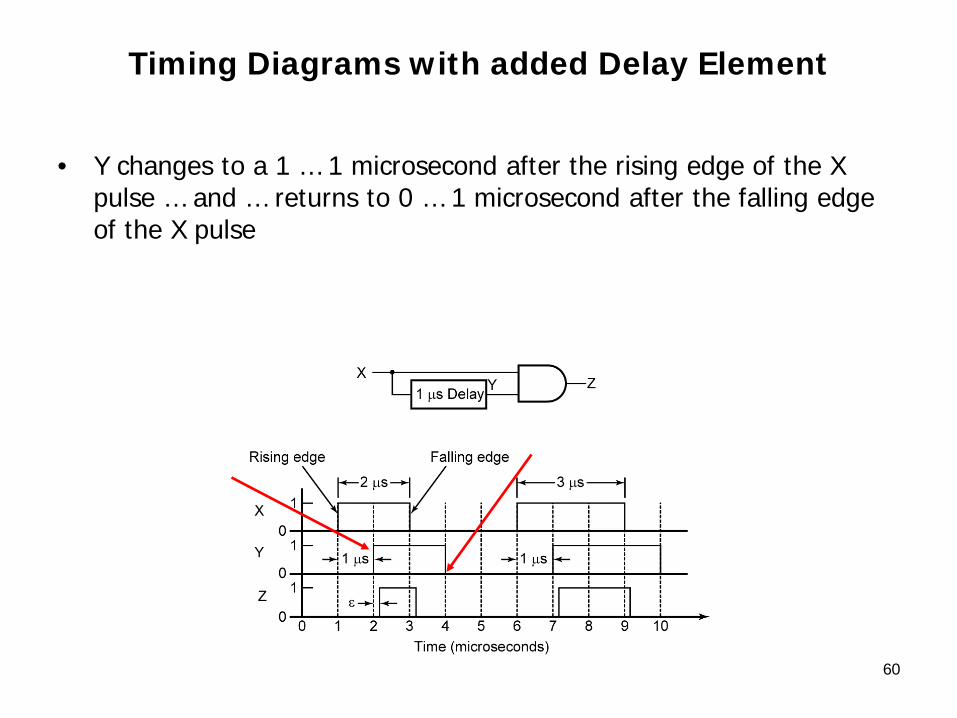
• Y changes to a 1 … 1 microsecond after the rising edge of the X pulse … and … returns to 0 … 1 microsecond after the falling edge of the X pulse
60
Timing Diagrams with added Delay Element
• Z will be 1 during the time interval in which both X and Y are 1
61
62
Hazards in Combinational Logic
Hazards in Combinational Logic
• When the input to a combinational circuit changes …
– Unwanted switching transients may appear in the output
• These transients occur when …
– Different paths from input to output have different propagation delays
63
Hazards in Combinational Logic
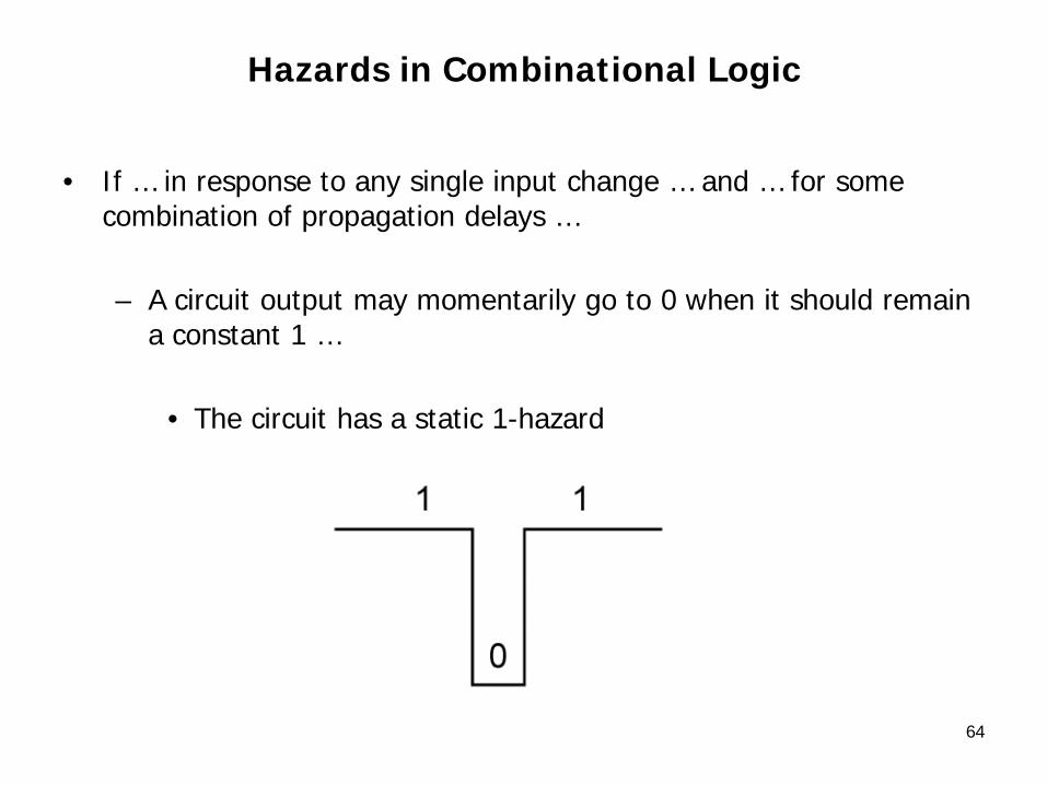
• If … in response to any single input change … and … for some combination of propagation delays …
– A circuit output may momentarily go to 0 when it should remain a constant 1 …
• The circuit has a static 1-hazard
64
Hazards in Combinational Logic
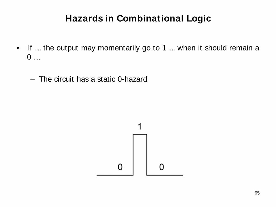
• If … the output may momentarily go to 1 … when it should remain a 0 …
– The circuit has a static 0-hazard
65
Hazards in Combinational Logic
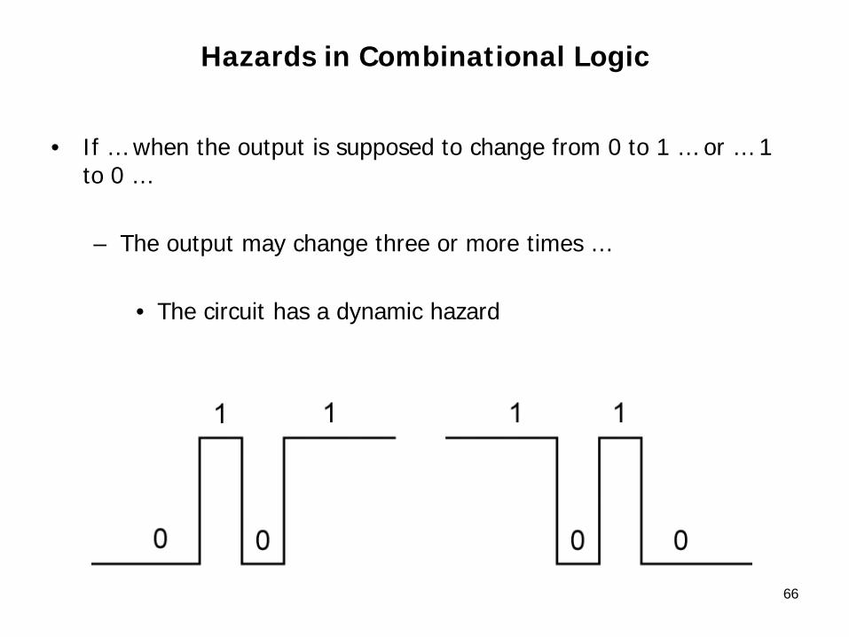
• If … when the output is supposed to change from 0 to 1 … or … 1 to 0 …
– The output may change three or more times …
• The circuit has a dynamic hazard
66
Hazards in Combinational Logic
• In each case the steady-state output of the circuit is correct …
– But … a switching transient appears at the circuit output when the input is changed
67

68
Detecting Hazards …
Detecting Hazards
• We can detect hazards in a two-level AND-OR circuit using the following procedure …
1. Write down the sum-of-products expression for the circuit
2. Plot each term on the K-map and loop it
3. If any two adjacent 1′s are not covered by the same loop, a 1-hazard exists for the transition between the two 1′s
• For an n-variable map … this transition occurs when one variable changes and the other n – 1 variables are held constant
69
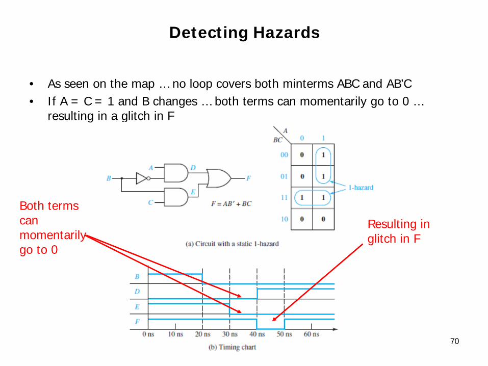
Detecting Hazards
• As seen on the map … no loop covers both minterms ABC and AB’C• If A = C = 1 and B changes … both terms can momentarily go to 0 …
resulting in a glitch in F
70
Both terms can momentarily go to 0
Resulting in glitch in F
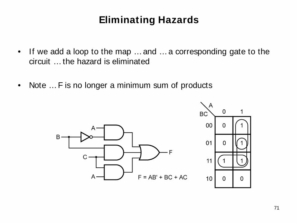
Eliminating Hazards
• If we add a loop to the map … and … a corresponding gate to the circuit … the hazard is eliminated
• Note … F is no longer a minimum sum of products
71

72
Eliminating Hazards …
73
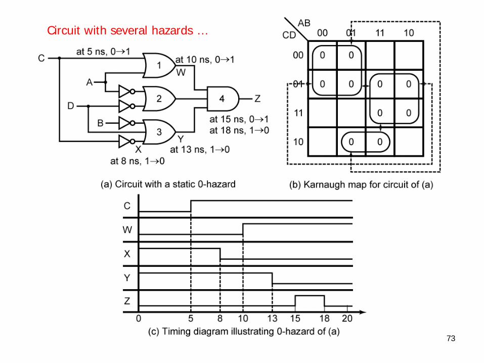
Circuit with several hazards …
74
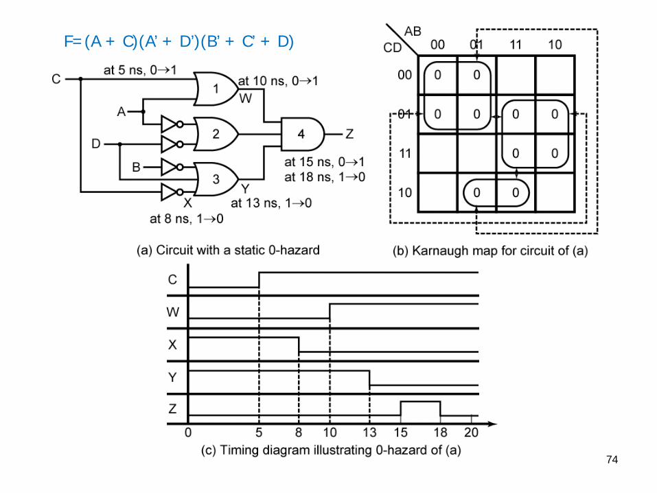
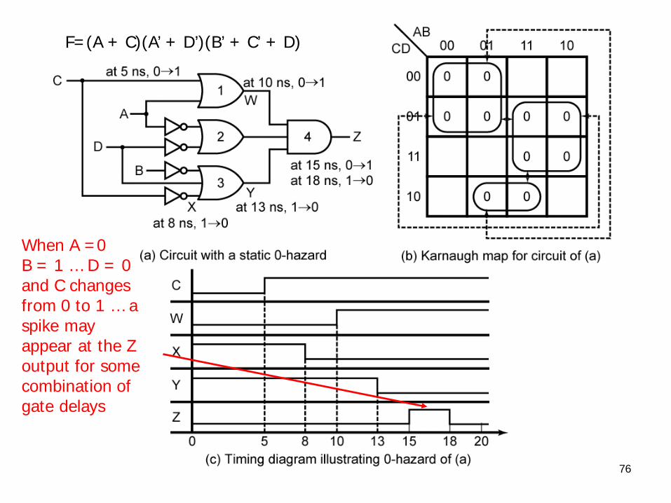
F=(A + C)(A’ + D’)(B’ + C’ + D)
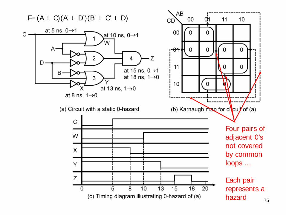
75
F=(A + C)(A’ + D’)(B’ + C’ + D)
Four pairs of adjacent 0’s not covered by common loops …
Each pair represents a hazard
76
F=(A + C)(A’ + D’)(B’ + C’ + D)
When A =0B = 1 … D = 0 and C changes from 0 to 1 … a spike may appear at the Z output for some combination of gate delays
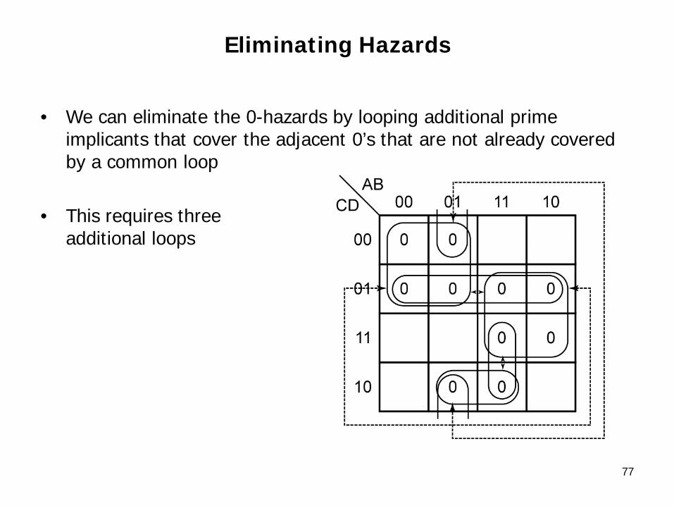
Eliminating Hazards
• We can eliminate the 0-hazards by looping additional prime implicants that cover the adjacent 0’s that are not already covered by a common loop
• This requires three additional loops
77
Eliminating Hazards
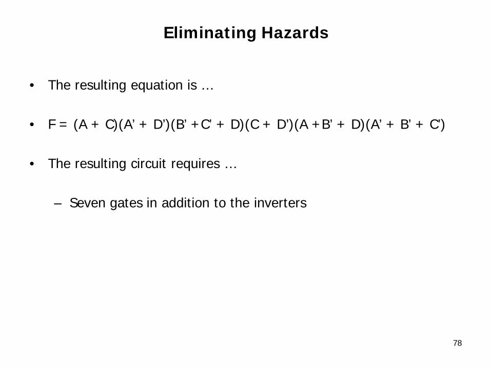
• The resulting equation is …
• F = (A + C)(A’ + D’)(B’ +C’ + D)(C + D’)(A +B’ + D)(A’ + B’ + C’)
• The resulting circuit requires …
– Seven gates in addition to the inverters
78

79
Designing a Circuit Free of Hazards …
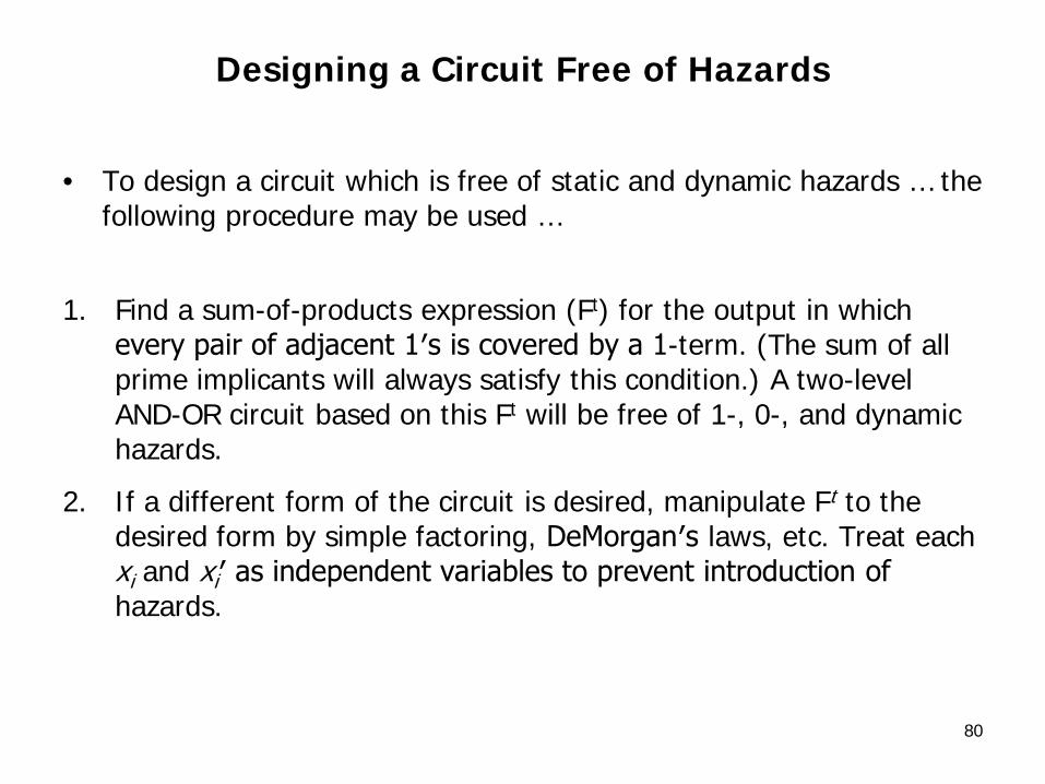
Designing a Circuit Free of Hazards
• To design a circuit which is free of static and dynamic hazards … the following procedure may be used …
1. Find a sum-of-products expression (Ft) for the output in which every pair of adjacent 1′s is covered by a 1-term. (The sum of all prime implicants will always satisfy this condition.) A two-level AND-OR circuit based on this Ft will be free of 1-, 0-, and dynamic hazards.
2. If a different form of the circuit is desired, manipulate Ft to the desired form by simple factoring, DeMorgan′s laws, etc. Treat each xi and xi′ as independent variables to prevent introduction of hazards.
80
81
Simulation and Testing of Logic Circuits …
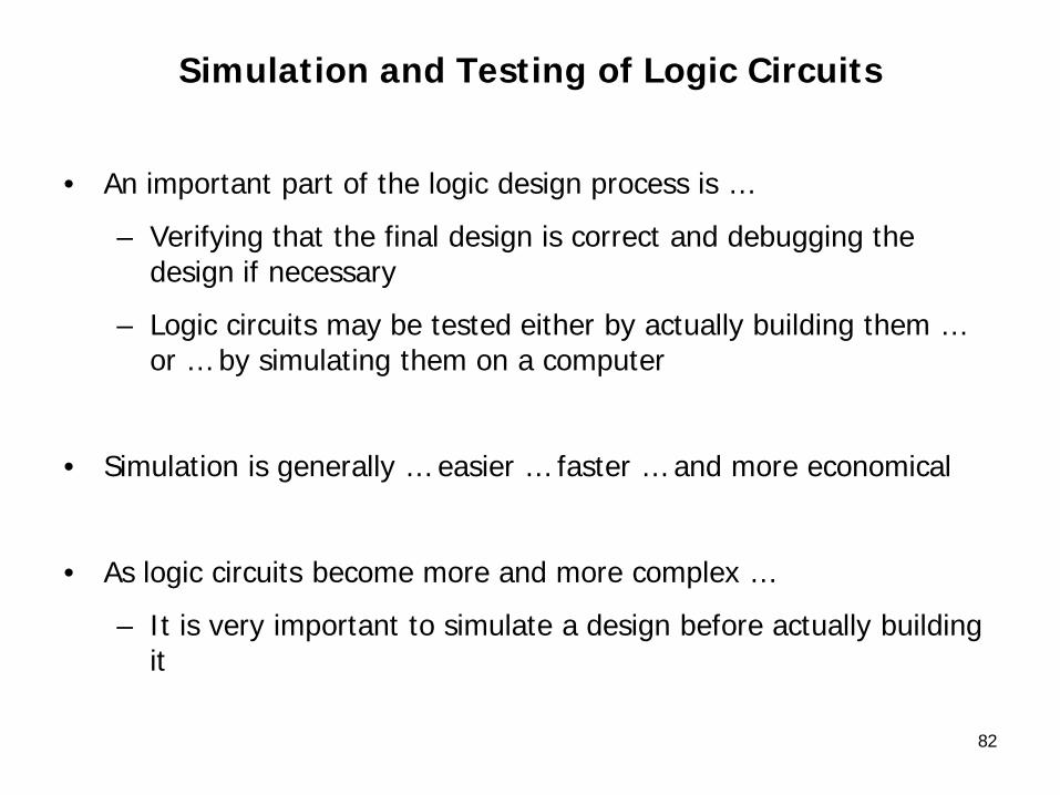
Simulation and Testing of Logic Circuits
• An important part of the logic design process is …
– Verifying that the final design is correct and debugging the design if necessary
– Logic circuits may be tested either by actually building them … or … by simulating them on a computer
• Simulation is generally … easier … faster … and more economical
• As logic circuits become more and more complex …
– It is very important to simulate a design before actually building it
82
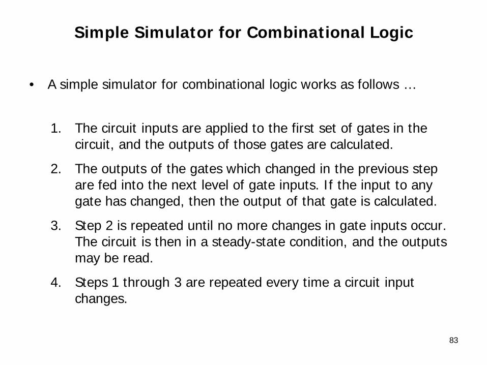
Simple Simulator for Combinational Logic
• A simple simulator for combinational logic works as follows …
1. The circuit inputs are applied to the first set of gates in the circuit, and the outputs of those gates are calculated.
2. The outputs of the gates which changed in the previous step are fed into the next level of gate inputs. If the input to any gate has changed, then the output of that gate is calculated.
3. Step 2 is repeated until no more changes in gate inputs occur. The circuit is then in a steady-state condition, and the outputs may be read.
4. Steps 1 through 3 are repeated every time a circuit input changes.
83
Simple Simulator for Combinational Logic
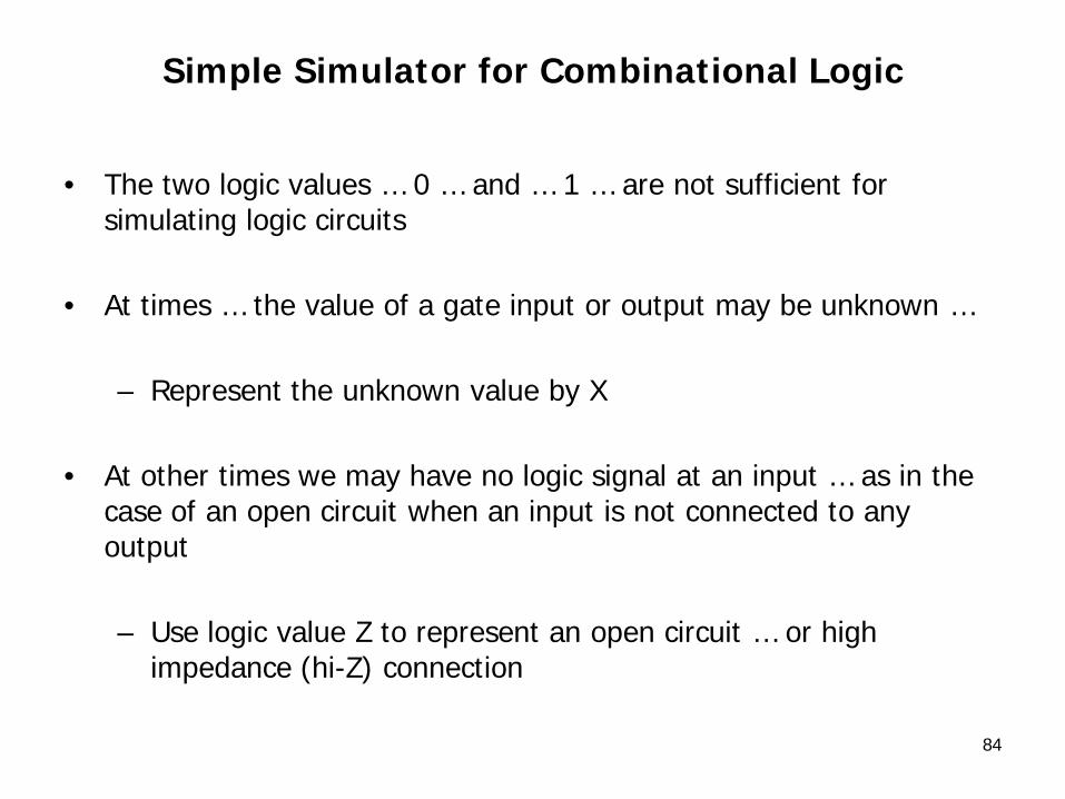
• The two logic values … 0 … and … 1 … are not sufficient for simulating logic circuits
• At times … the value of a gate input or output may be unknown …
– Represent the unknown value by X
• At other times we may have no logic signal at an input … as in the case of an open circuit when an input is not connected to any output
– Use logic value Z to represent an open circuit … or high impedance (hi-Z) connection
84
Four-Valued Logic Simulation
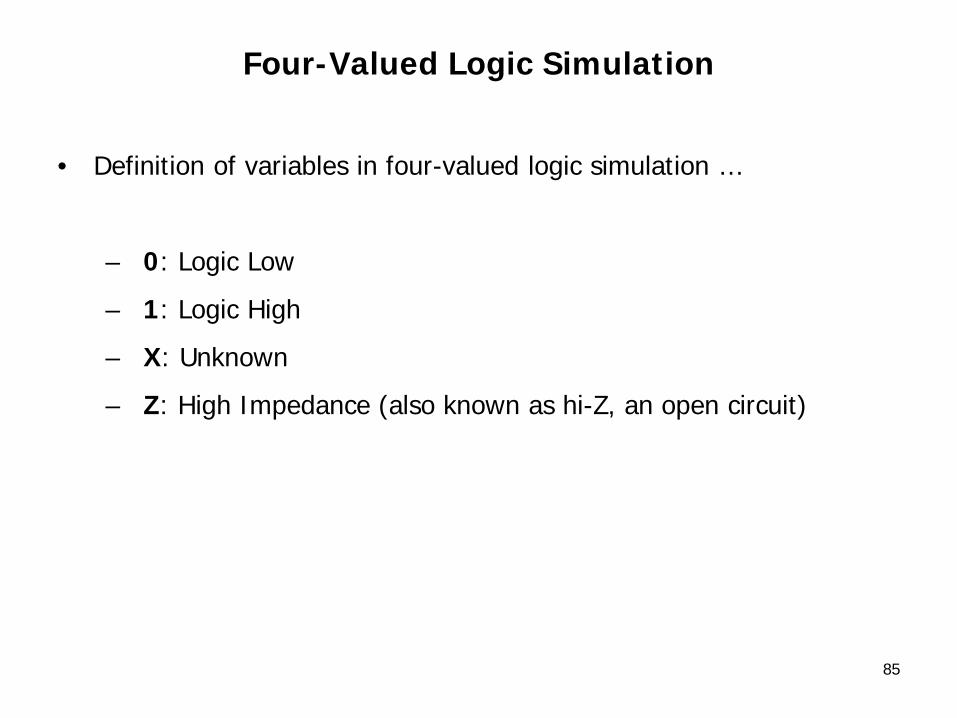
• Definition of variables in four-valued logic simulation …
– 0: Logic Low
– 1: Logic High
– X: Unknown
– Z: High Impedance (also known as hi-Z, an open circuit)
85
Simple Simulator for Combinational Logic
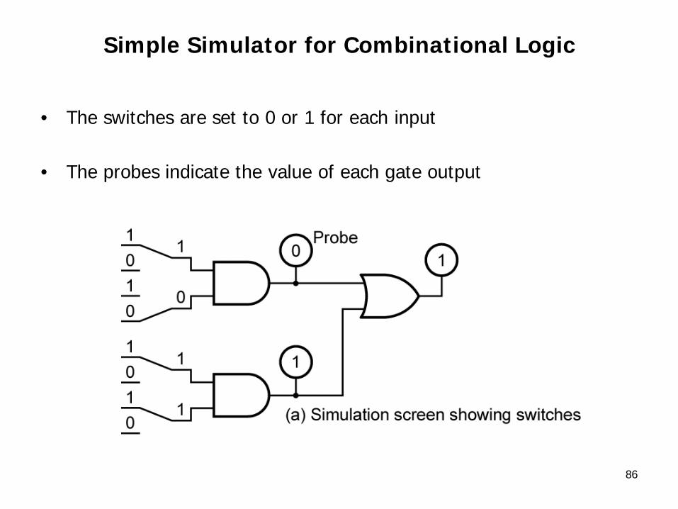
• The switches are set to 0 or 1 for each input
• The probes indicate the value of each gate output
86
Simple Simulator for Combinational Logic
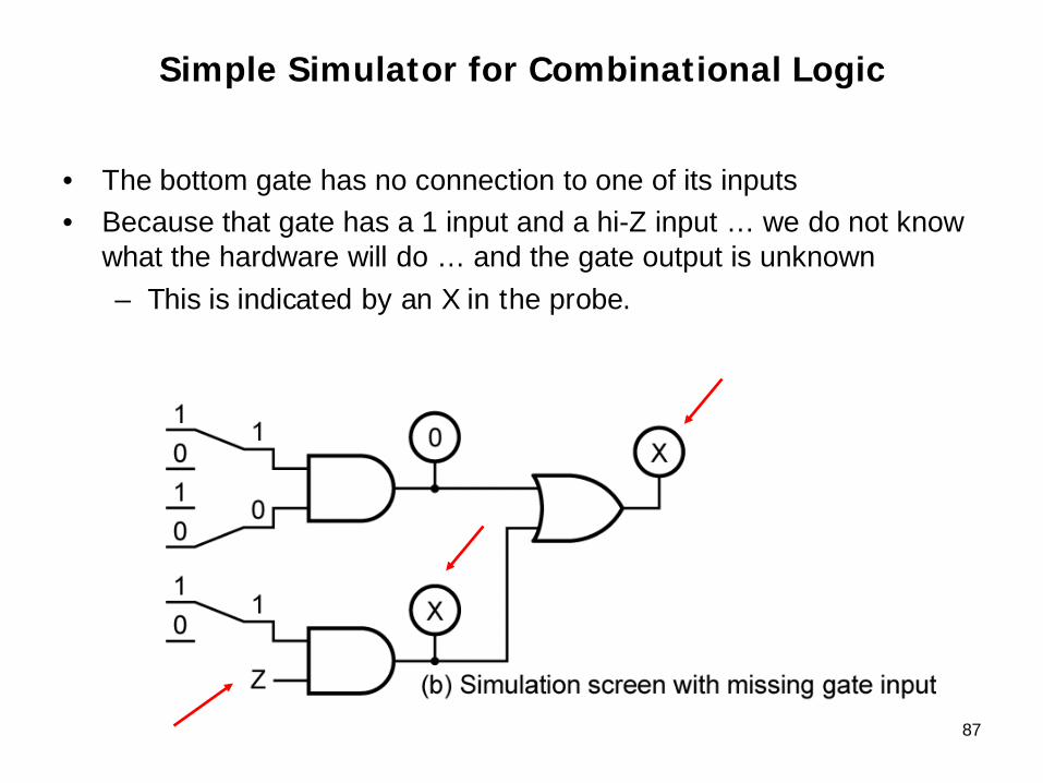
• The bottom gate has no connection to one of its inputs• Because that gate has a 1 input and a hi-Z input … we do not know
what the hardware will do … and the gate output is unknown– This is indicated by an X in the probe.
87

88
AND Function for Four-Valued Simulation …
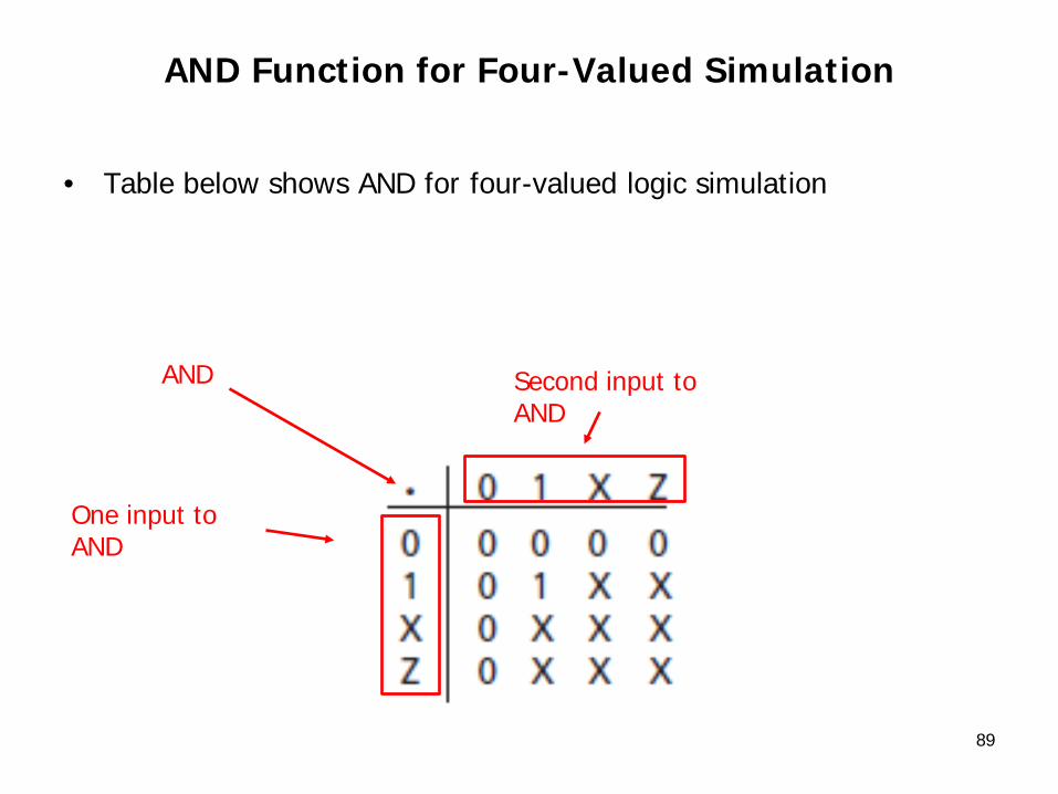
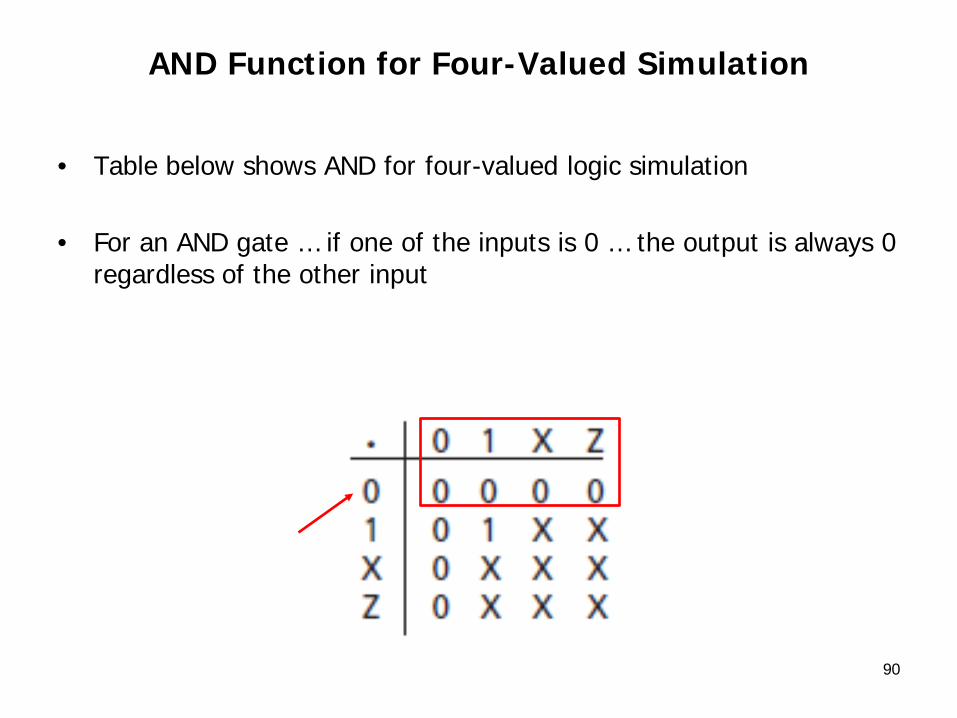
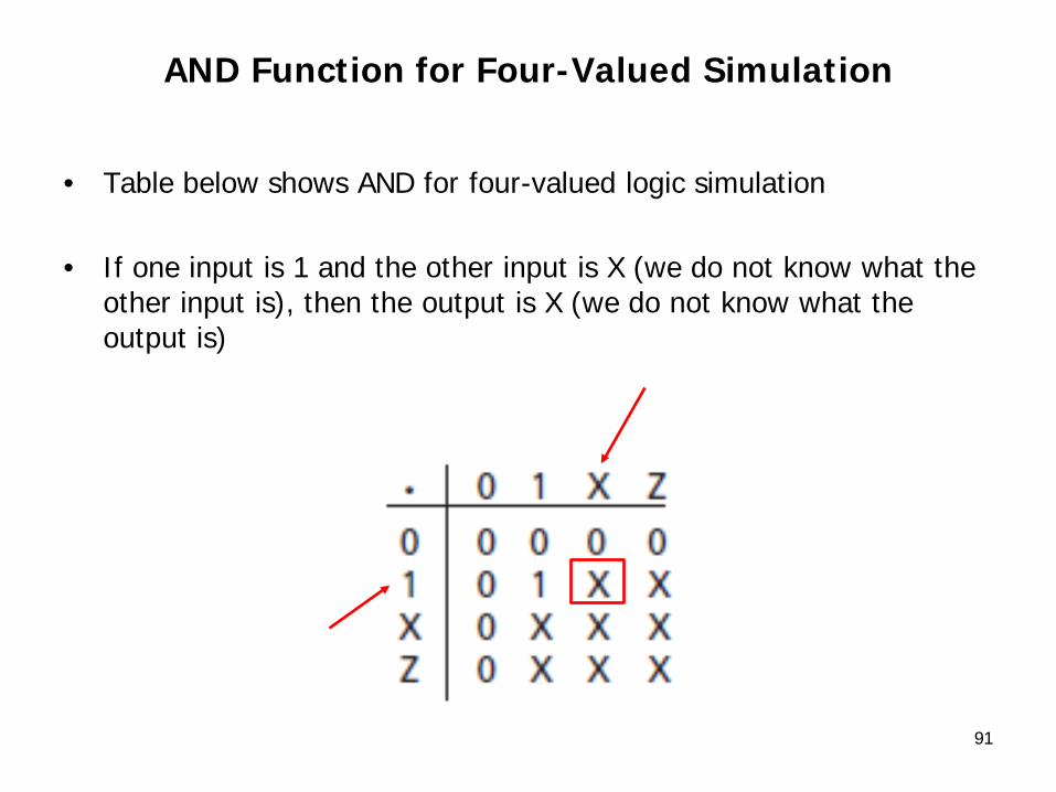
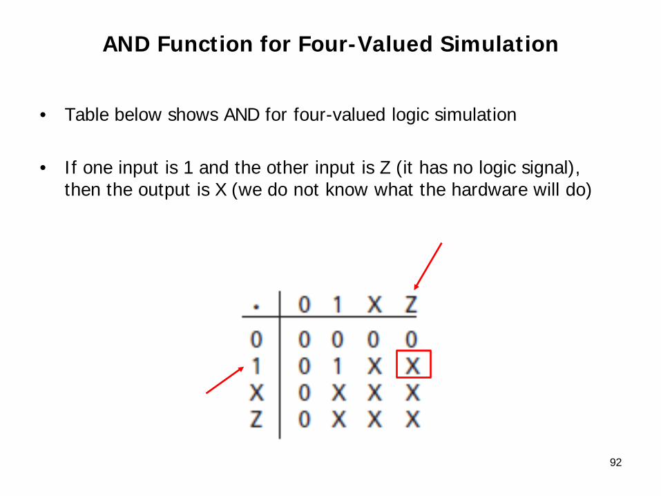
AND Function for Four-Valued Simulation
• Table below shows AND for four-valued logic simulation
89
One input to AND
Second input to AND
AND
AND Function for Four-Valued Simulation
• Table below shows AND for four-valued logic simulation
• For an AND gate … if one of the inputs is 0 … the output is always 0 regardless of the other input
90
AND Function for Four-Valued Simulation
• Table below shows AND for four-valued logic simulation
• If one input is 1 and the other input is X (we do not know what the other input is), then the output is X (we do not know what the output is)
91
AND Function for Four-Valued Simulation
• Table below shows AND for four-valued logic simulation
• If one input is 1 and the other input is Z (it has no logic signal), then the output is X (we do not know what the hardware will do)
92

93
OR Function for Four-Valued Simulation …
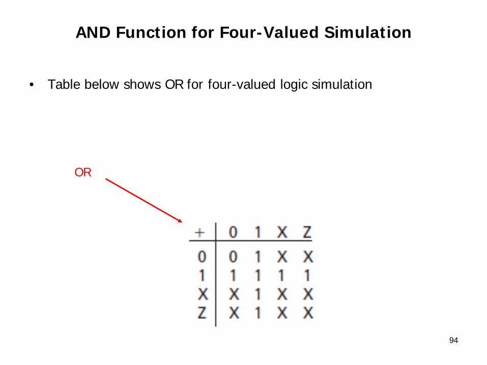
AND Function for Four-Valued Simulation
• Table below shows OR for four-valued logic simulation
94
OR

95
Possible Causes for an Incorrect Output …
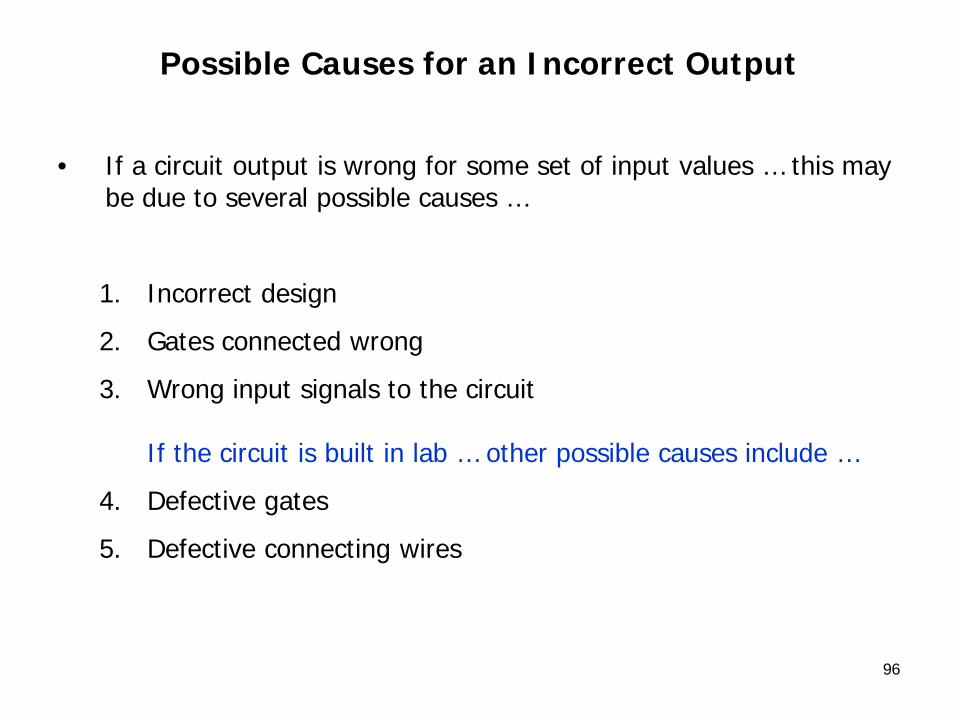
Possible Causes for an Incorrect Output
• If a circuit output is wrong for some set of input values … this may be due to several possible causes …
1. Incorrect design
2. Gates connected wrong
3. Wrong input signals to the circuit
If the circuit is built in lab … other possible causes include …
4. Defective gates
5. Defective connecting wires
96
97
Example … Locating Cause for an Incorrect Output …
Example … Locating Cause for an Incorrect Output
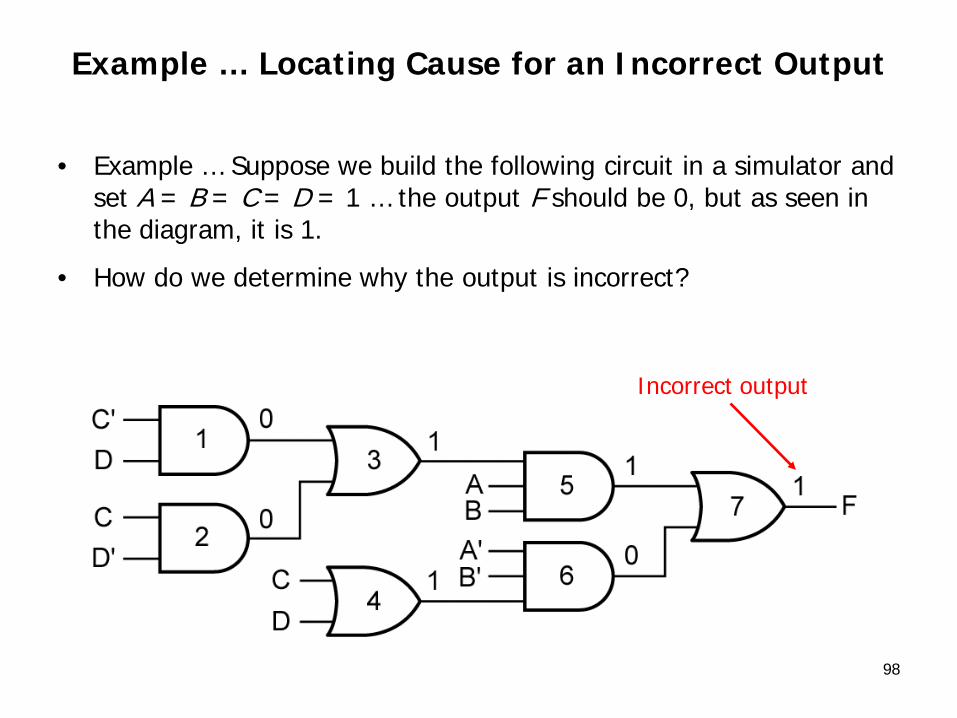
• Example … Suppose we build the following circuit in a simulator and set A = B = C = D = 1 … the output F should be 0, but as seen in the diagram, it is 1.
• How do we determine why the output is incorrect?
98
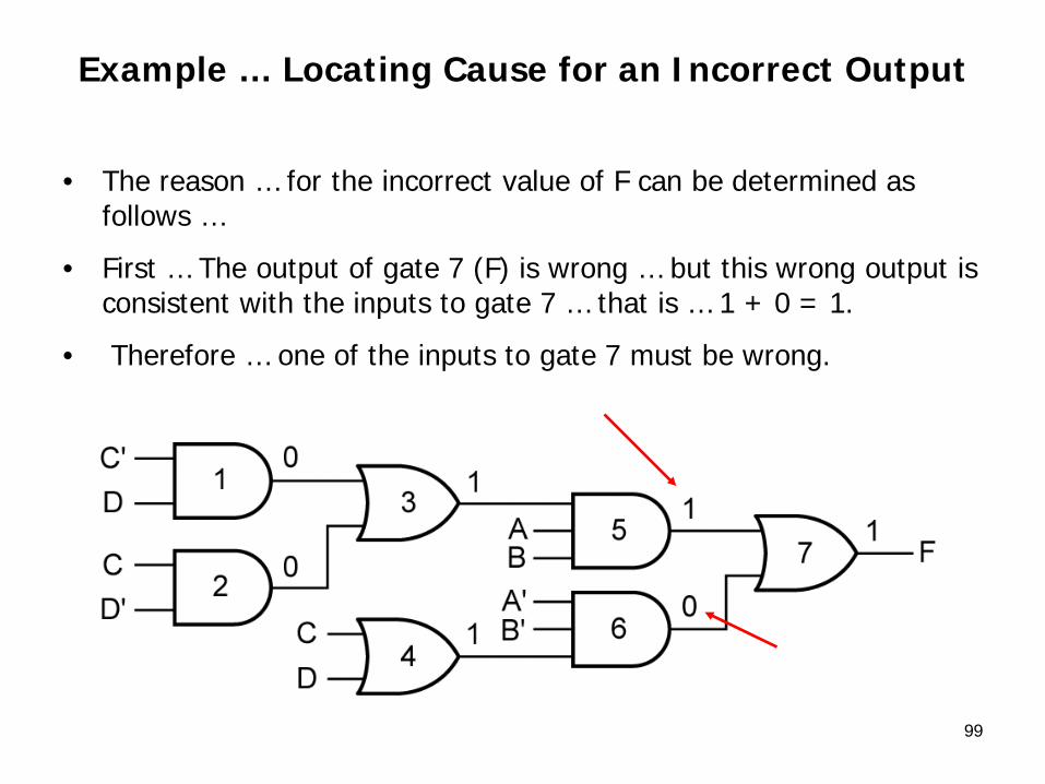
Incorrect output
Example … Locating Cause for an Incorrect Output
• The reason … for the incorrect value of F can be determined as follows …
• First … The output of gate 7 (F) is wrong … but this wrong output is consistent with the inputs to gate 7 … that is … 1 + 0 = 1.
• Therefore … one of the inputs to gate 7 must be wrong.
99
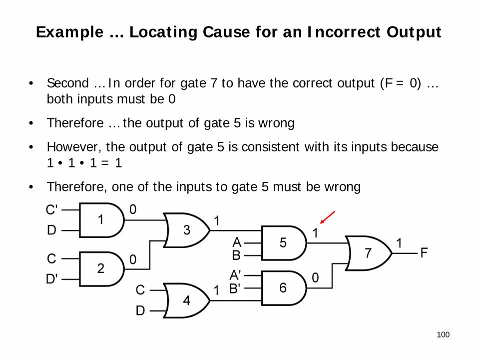
Example … Locating Cause for an Incorrect Output
• Second … In order for gate 7 to have the correct output (F = 0) … both inputs must be 0
• Therefore … the output of gate 5 is wrong
• However, the output of gate 5 is consistent with its inputs because 1 • 1 • 1 = 1
• Therefore, one of the inputs to gate 5 must be wrong
100
Example … Locating Cause for an Incorrect Output
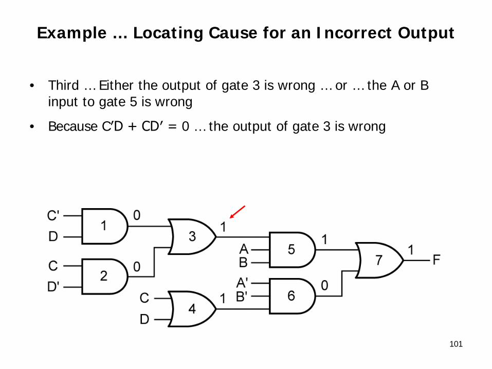
• Third … Either the output of gate 3 is wrong … or … the A or B input to gate 5 is wrong
• Because C′D + CD′ = 0 … the output of gate 3 is wrong
101
Example … Locating Cause for an Incorrect Output
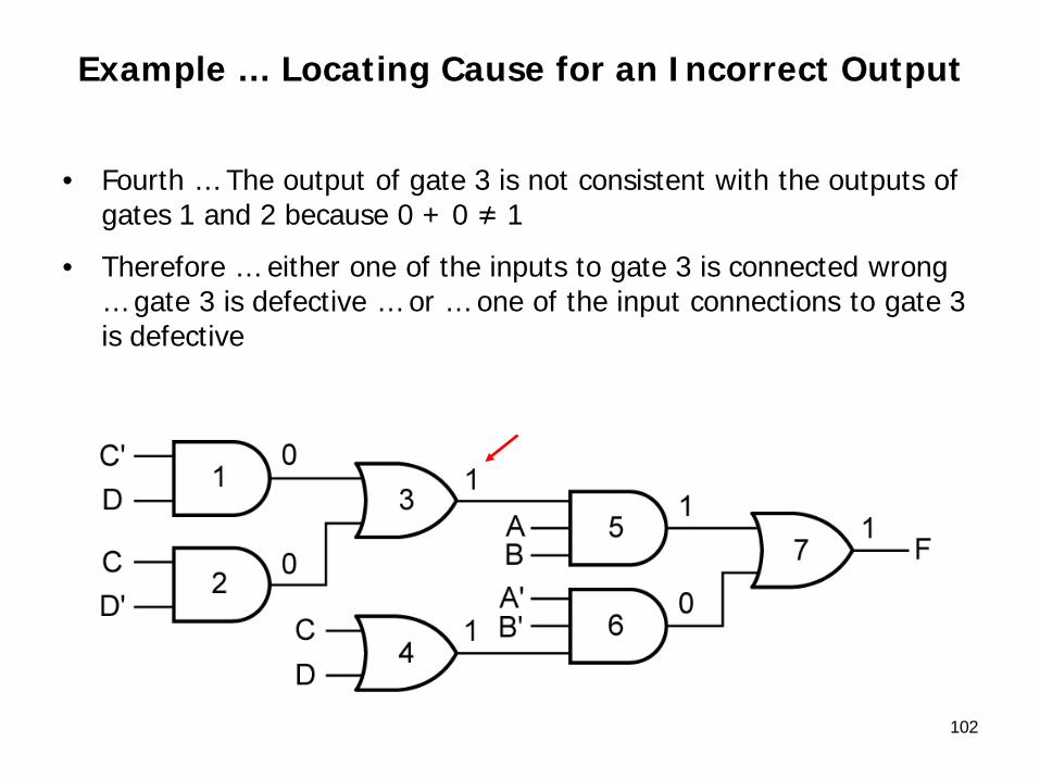
• Fourth … The output of gate 3 is not consistent with the outputs of gates 1 and 2 because 0 + 0 ≠ 1
• Therefore … either one of the inputs to gate 3 is connected wrong … gate 3 is defective … or … one of the input connections to gate 3 is defective
102
Example … Locating Cause for an Incorrect Output
• The prior example … illustrates how to troubleshoot a logic circuit by …
– Starting at the output gate .. and …
– Working back until the wrong connection or defective gate is located
103
104
Lab

Lab
• Any issues with Lab #1 thus far???
• Last week …
– Lab Booklets were passed out
– RECALL … Use Student Logic Number 301
– Lab report criteria is available on the class web page
105

106
Next Week …

107
Next Week Topics
• Chapter 9 … Multiplexers, Decoders, Encoder, and PLD

108
Home Work

109
Homework
1. Lab #1
2. Read Chapter 9

110
References
1. None