Embed Size (px)
Citation preview
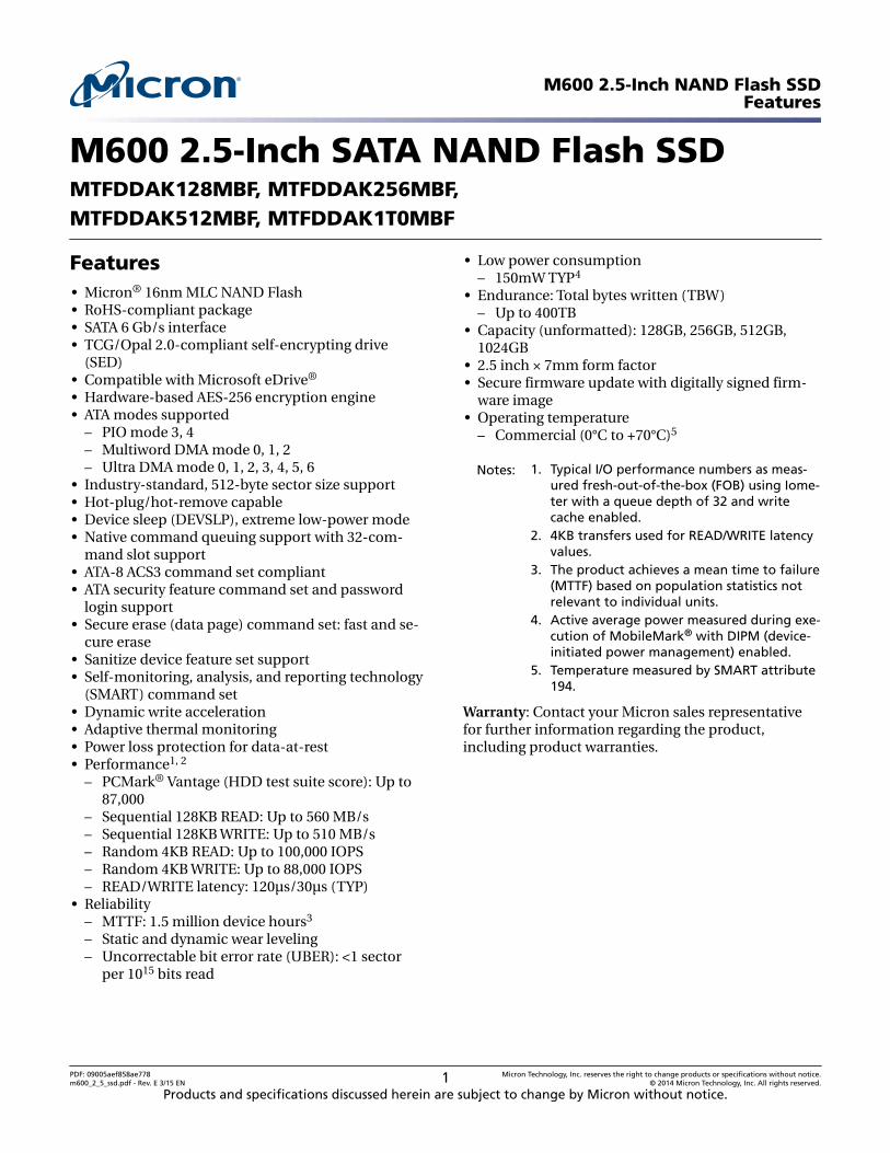
M600 2.5-Inch SATA NAND Flash SSDMTFDDAK128MBF, MTFDDAK256MBF,MTFDDAK512MBF, MTFDDAK1T0MBF
Features• Micron® 16nm MLC NAND Flash• RoHS-compliant package• SATA 6 Gb/s interface• TCG/Opal 2.0-compliant self-encrypting drive
(SED)• Compatible with Microsoft eDrive®
• Hardware-based AES-256 encryption engine• ATA modes supported
– PIO mode 3, 4– Multiword DMA mode 0, 1, 2– Ultra DMA mode 0, 1, 2, 3, 4, 5, 6
• Industry-standard, 512-byte sector size support• Hot-plug/hot-remove capable• Device sleep (DEVSLP), extreme low-power mode• Native command queuing support with 32-com-
mand slot support• ATA-8 ACS3 command set compliant• ATA security feature command set and password
login support• Secure erase (data page) command set: fast and se-
cure erase• Sanitize device feature set support• Self-monitoring, analysis, and reporting technology
(SMART) command set• Dynamic write acceleration• Adaptive thermal monitoring• Power loss protection for data-at-rest• Performance1, 2
– PCMark® Vantage (HDD test suite score): Up to87,000
– Sequential 128KB READ: Up to 560 MB/s– Sequential 128KB WRITE: Up to 510 MB/s– Random 4KB READ: Up to 100,000 IOPS– Random 4KB WRITE: Up to 88,000 IOPS– READ/WRITE latency: 120µs/30µs (TYP)
• Reliability– MTTF: 1.5 million device hours3
– Static and dynamic wear leveling– Uncorrectable bit error rate (UBER): <1 sector
per 1015 bits read
• Low power consumption– 150mW TYP4
• Endurance: Total bytes written (TBW)– Up to 400TB
• Capacity (unformatted): 128GB, 256GB, 512GB,1024GB
• 2.5 inch × 7mm form factor• Secure firmware update with digitally signed firm-
ware image• Operating temperature
– Commercial (0°C to +70°C)5
Notes: 1. Typical I/O performance numbers as meas-ured fresh-out-of-the-box (FOB) using Iome-ter with a queue depth of 32 and writecache enabled.
2. 4KB transfers used for READ/WRITE latencyvalues.
3. The product achieves a mean time to failure(MTTF) based on population statistics notrelevant to individual units.
4. Active average power measured during exe-cution of MobileMark® with DIPM (device-initiated power management) enabled.
5. Temperature measured by SMART attribute194.
Warranty: Contact your Micron sales representativefor further information regarding the product,including product warranties.
M600 2.5-Inch NAND Flash SSDFeatures
PDF: 09005aef858ae778m600_2_5_ssd.pdf - Rev. E 3/15 EN 1 Micron Technology, Inc. reserves the right to change products or specifications without notice.
© 2014 Micron Technology, Inc. All rights reserved.
Products and specifications discussed herein are subject to change by Micron without notice.
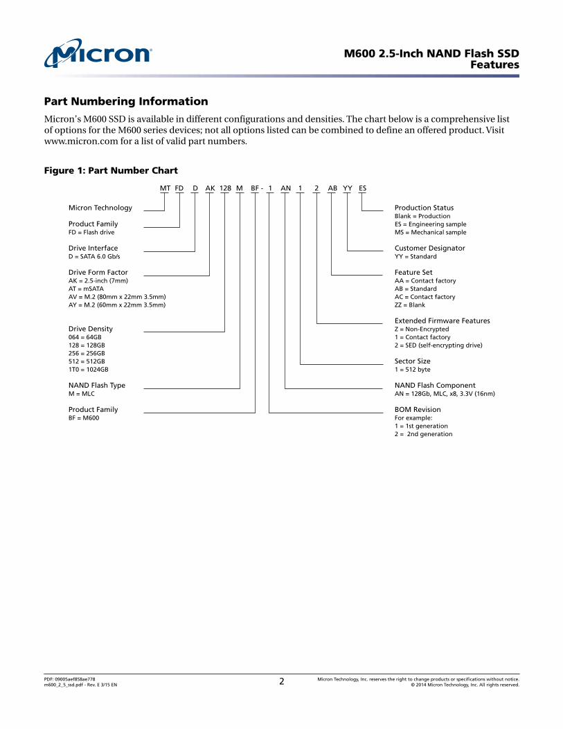
Part Numbering Information
Micron’s M600 SSD is available in different configurations and densities. The chart below is a comprehensive listof options for the M600 series devices; not all options listed can be combined to define an offered product. Visit www.micron.com for a list of valid part numbers.
Figure 1: Part Number Chart
MT FD D AK 128 M BF - 1 AN 1 ES
Micron Technology
Product FamilyFD = Flash drive
Drive InterfaceD = SATA 6.0 Gb/s
Drive Form FactorAK = 2.5-inch (7mm)AT = mSATAAV = M.2 (80mm x 22mm 3.5mm)AY = M.2 (60mm x 22mm 3.5mm)
Drive Density064 = 64GB128 = 128GB256 = 256GB512 = 512GB1T0 = 1024GB
NAND Flash TypeM = MLC
Product FamilyBF = M600
Production StatusBlank = ProductionES = Engineering sampleMS = Mechanical sample
Customer DesignatorYY = Standard
Feature SetAA = Contact factoryAB = StandardAC = Contact factoryZZ = Blank
Extended Firmware FeaturesZ = Non-Encrypted1 = Contact factory2 = SED (self-encrypting drive)
Sector Size1 = 512 byte
NAND Flash ComponentAN = 128Gb, MLC, x8, 3.3V (16nm)
BOM RevisionFor example:1 = 1st generation2 = 2nd generation
2 AB YY
M600 2.5-Inch NAND Flash SSDFeatures
PDF: 09005aef858ae778m600_2_5_ssd.pdf - Rev. E 3/15 EN 2 Micron Technology, Inc. reserves the right to change products or specifications without notice.
© 2014 Micron Technology, Inc. All rights reserved.
General DescriptionMicron’s solid state drive (SSD) uses a single-chip controller with a SATA interface onthe system side and eight channels of Micron NAND Flash internally. Packaged in anHDD replacement enclosure, the SSD integrates easily in existing storage infrastruc-tures.
The SSD is designed to use the SATA interface efficiently during both READs andWRITEs while delivering bandwidth-focused performance. SSD technology enables en-hanced boot times, faster application load times, reduced power consumption, and ex-tended reliability.
The self-encrypting drive (SED) features a FIPS-compliant, AES-256 encryption engine,providing hardware-based, secure data encryption, with no loss of SSD performance.This SED follows the TCG/Opal specification for trusted peripherals.
When TCG/Opal features are not enabled, the device can perform alternate data en-cryption by invoking the ATA security command set encryption features, to provide full-disk encryption (FDE) managed in the host system BIOS. TCG/Opal and ATA securityfeature sets cannot be enabled simultaneously.
The data encryption is always running; however, encryption keys are not managed andthe data is not secure until either TCG/Opal or ATA security feature sets are enabled.
Figure 2: Functional Block Diagram
NAND
SATA
NAND
NAND
NAND
SSDcontroller
DRAMbuffer
NAND
M600 2.5-Inch NAND Flash SSDGeneral Description
PDF: 09005aef858ae778m600_2_5_ssd.pdf - Rev. E 3/15 EN 3 Micron Technology, Inc. reserves the right to change products or specifications without notice.
© 2014 Micron Technology, Inc. All rights reserved.
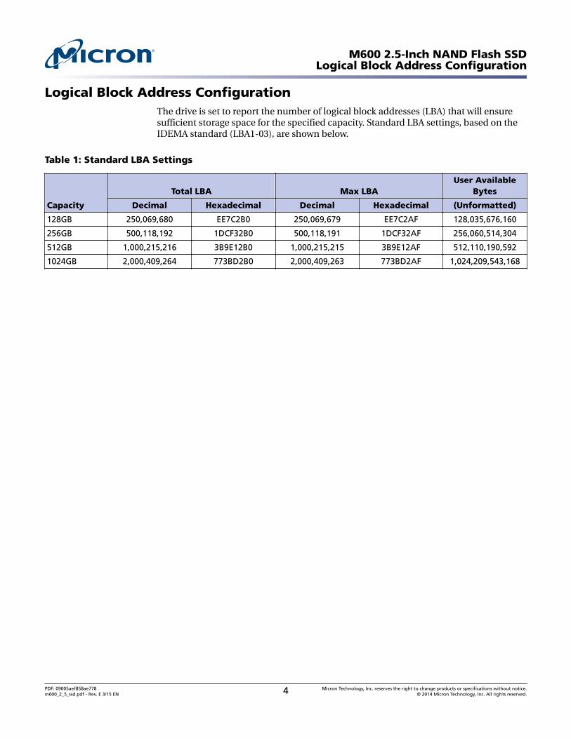
Logical Block Address ConfigurationThe drive is set to report the number of logical block addresses (LBA) that will ensuresufficient storage space for the specified capacity. Standard LBA settings, based on theIDEMA standard (LBA1-03), are shown below.
Table 1: Standard LBA Settings
Capacity
Total LBA Max LBAUser Available
Bytes
Decimal Hexadecimal Decimal Hexadecimal (Unformatted)
128GB 250,069,680 EE7C2B0 250,069,679 EE7C2AF 128,035,676,160
256GB 500,118,192 1DCF32B0 500,118,191 1DCF32AF 256,060,514,304
512GB 1,000,215,216 3B9E12B0 1,000,215,215 3B9E12AF 512,110,190,592
1024GB 2,000,409,264 773BD2B0 2,000,409,263 773BD2AF 1,024,209,543,168
M600 2.5-Inch NAND Flash SSDLogical Block Address Configuration
PDF: 09005aef858ae778m600_2_5_ssd.pdf - Rev. E 3/15 EN 4 Micron Technology, Inc. reserves the right to change products or specifications without notice.
© 2014 Micron Technology, Inc. All rights reserved.
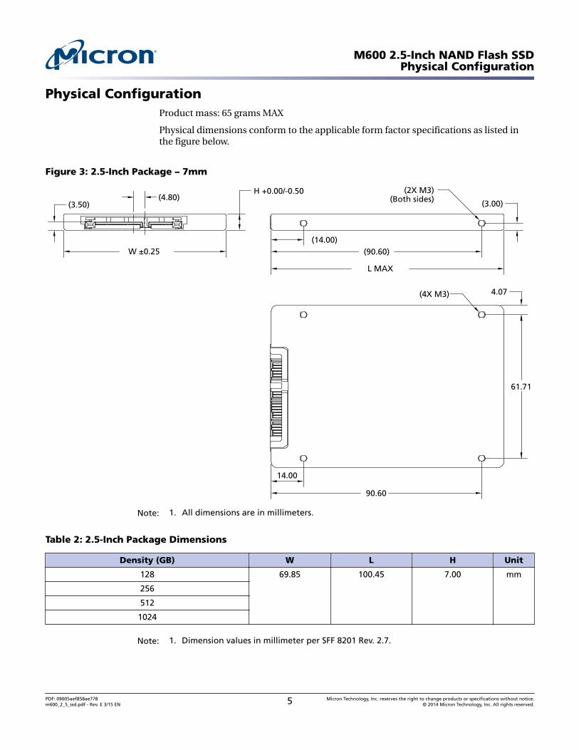
Physical ConfigurationProduct mass: 65 grams MAX
Physical dimensions conform to the applicable form factor specifications as listed inthe figure below.
Figure 3: 2.5-Inch Package – 7mm
H +0.00/-0.50
L MAX
W ±0.25
(3.50)(4.80)
(14.00)(90.60)
(2X M3)(Both sides) (3.00)
14.00
90.60
61.71
4.07(4X M3)
Note: 1. All dimensions are in millimeters.
Table 2: 2.5-Inch Package Dimensions
Density (GB) W L H Unit
128 69.85 100.45 7.00 mm
256
512
1024
Note: 1. Dimension values in millimeter per SFF 8201 Rev. 2.7.
M600 2.5-Inch NAND Flash SSDPhysical Configuration
PDF: 09005aef858ae778m600_2_5_ssd.pdf - Rev. E 3/15 EN 5 Micron Technology, Inc. reserves the right to change products or specifications without notice.
© 2014 Micron Technology, Inc. All rights reserved.
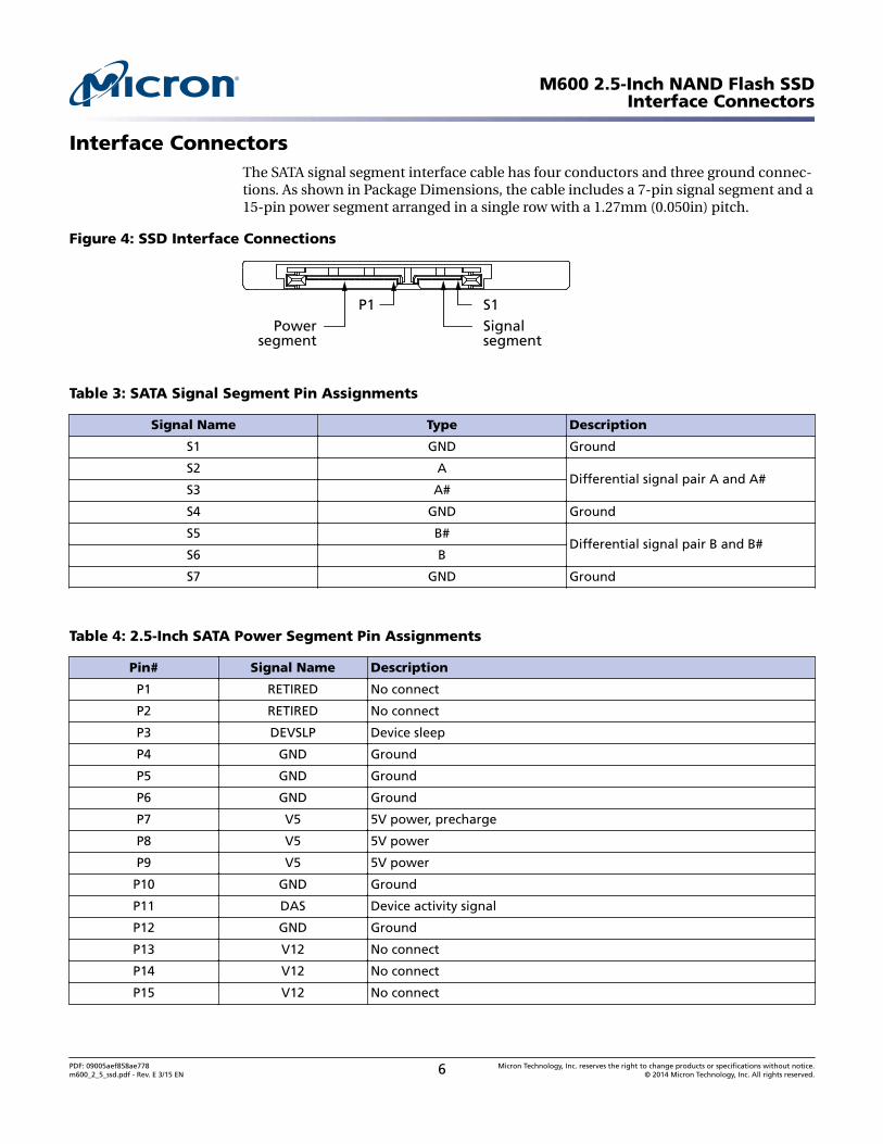
Interface ConnectorsThe SATA signal segment interface cable has four conductors and three ground connec-tions. As shown in Package Dimensions, the cable includes a 7-pin signal segment and a15-pin power segment arranged in a single row with a 1.27mm (0.050in) pitch.
Figure 4: SSD Interface Connections
Powersegment
Signalsegment
P1 S1
Table 3: SATA Signal Segment Pin Assignments
Signal Name Type Description
S1 GND Ground
S2 ADifferential signal pair A and A#
S3 A#
S4 GND Ground
S5 B#Differential signal pair B and B#
S6 B
S7 GND Ground
Table 4: 2.5-Inch SATA Power Segment Pin Assignments
Pin# Signal Name Description
P1 RETIRED No connect
P2 RETIRED No connect
P3 DEVSLP Device sleep
P4 GND Ground
P5 GND Ground
P6 GND Ground
P7 V5 5V power, precharge
P8 V5 5V power
P9 V5 5V power
P10 GND Ground
P11 DAS Device activity signal
P12 GND Ground
P13 V12 No connect
P14 V12 No connect
P15 V12 No connect
M600 2.5-Inch NAND Flash SSDInterface Connectors
PDF: 09005aef858ae778m600_2_5_ssd.pdf - Rev. E 3/15 EN 6 Micron Technology, Inc. reserves the right to change products or specifications without notice.
© 2014 Micron Technology, Inc. All rights reserved.
PerformanceMeasured performance can vary for a number of reasons. The major factors affectingdrive performance are the capacity of the drive and the interface of the host. Addition-ally, overall system performance can affect the measured drive performance. Whencomparing drives, it is recommended that all system variables are the same, and onlythe drive being tested varies.
Performance numbers will vary depending on the host system configuration.
For SSDs designed for the client computing market, Micron specifies performance infresh-out-of-box (FOB) state. Data throughput measured in "steady state" may be lowerthan FOB state, depending on the nature of the data workload.
For a description of these performance states and of Micron's best practices for per-formance measurement, refer to Micron's technical marketing brief "Best Practices forSSD Performance Measurement"(www.micron.com/products/solid-state-storage/).
Table 5: Drive Performance
Capacity 128GB 256GB 512GB 1024GB
UnitInterface Speed 6 Gb/s 6 Gb/s 6 Gb/s 6 Gb/s
PCMark Vantage 87,000 87,000 87,000 87,000 HDD score
Sequential read (128KB transfer) 560 560 560 560 MB/s
Sequential write (128KB transfer) 400 510 510 510 MB/s
Random read (4KB transfer) 90,000 100,000 100,000 100,000 IOPS
Random write (4KB transfer) 88,000 88,000 88,000 88,000 IOPS
READ latency (TYP) 120 120 120 120 µs
WRITE latency (TYP) 30 30 30 30 µs
Notes: 1. Performance numbers are maximum values, except as noted.2. Typical I/O performance numbers as measured using Iometer with a queue depth of 32
and write cache enabled. Fresh-out-of-box (FOB) state is assumed. For performancemeasurement purposes, the SSD may be restored to FOB state using the SECURE ERASEcommand.
3. Iometer measurements are performed on an 20GB span of logical block addresses(LBAs).
4. 4KB transfers with a queue depth of 1 are used to measure READ/WRITE latency valueswith write cache enabled.
5. System variations will affect measured results. For comparison, PCMark scores are meas-ured with the SSD as a secondary drive in a two-drive system. When measured as an OSdrive, system overhead can cause lower scores.
M600 2.5-Inch NAND Flash SSDPerformance
PDF: 09005aef858ae778m600_2_5_ssd.pdf - Rev. E 3/15 EN 7 Micron Technology, Inc. reserves the right to change products or specifications without notice.
© 2014 Micron Technology, Inc. All rights reserved.
ReliabilityMicron’s SSDs incorporate advanced technology for defect and error management.They use various combinations of hardware-based error correction algorithms andfirmware-based static and dynamic wear-leveling algorithms.
Over the life of the SSD, uncorrectable errors may occur. An uncorrectable error is de-fined as data that is reported as successfully programmed to the SSD but when it is readout of the SSD, the data differs from what was programmed.
Table 6: Uncorrectable Bit Error Rate
Uncorrectable Bit Error Rate Operation
<1 sector per 1015 bits read READ
Mean Time To Failure
Mean time to failure (MTTF) for the SSD can be predicted based on the component reli-ability data using the methods referenced in the Telcordia SR-332 reliability predictionprocedures for electronic equipment.
Table 7: MTTF
Capacity MTTF (Operating Hours)1
128GB 1.5 million
256GB 1.5 million
512GB 1.5 million
1024GB 1.5 million
Note: 1. The product achieves a mean time to failure (MTTF) of 1.5 million hours, based on popu-lation statistics not relevant to individual units.
M600 2.5-Inch NAND Flash SSDReliability
PDF: 09005aef858ae778m600_2_5_ssd.pdf - Rev. E 3/15 EN 8 Micron Technology, Inc. reserves the right to change products or specifications without notice.
© 2014 Micron Technology, Inc. All rights reserved.
Endurance
Endurance for the SSD can be predicted based on the usage conditions applied to thedevice, the internal NAND component cycles, the write amplification factor, and thewear-leveling efficiency of the drive. The table below shows the drive lifetime for eachSSD capacity by client computing and sequential input and based on predefined usageconditions.
Table 8: Drive Lifetime – Client Computing
Capacity Drive Lifetime (Total Bytes Written)
128GB 100TB
256GB 200TB
512GB 300TB
1024GB 400TB
Notes: 1. Total bytes written validated with the drive 90% full.2. SSD volatile write cache is enabled.3. Access patterns used during reliability testing are 25% sequential and 75% random and
consist of the following: 50% are 4 KiB; 40% are 64 KiB; and 10% are 128 KiB.4. Host workload parameters, including write cache settings, I/O alignment, transfer sizes,
randomness, and percent full, that are substantially different than the described notesmay result in varied endurance results.
5. GB/day can be calculated by dividing the total bytes written value by (365 × number ofyears). For example: 100 TB/5 years/365 days = 54 GB/day for 5 years.
M600 2.5-Inch NAND Flash SSDReliability
PDF: 09005aef858ae778m600_2_5_ssd.pdf - Rev. E 3/15 EN 9 Micron Technology, Inc. reserves the right to change products or specifications without notice.
© 2014 Micron Technology, Inc. All rights reserved.
Electrical CharacteristicsEnvironmental conditions beyond those listed may cause permanent damage to the de-vice. This is a stress rating only, and functional operation of the device at these or anyother conditions above those indicated in the operational sections of this specificationis not implied. Exposure to absolute maximum rating conditions for extended periodsmay affect reliability.
Table 9: SATA Power Consumption
CapacityDevice Sleep
Typical Idle Average Active AverageActive Maximum(128KB transfer) Unit
128GB 2 70 150 3600 mW
256GB 2 70 150 4400 mW
512GB 2 70 150 4700 mW
1024GB 4 70 150 5200 mW
Notes: 1. Data taken at 25°C using a 6 Gb/s SATA interface.2. Active average power measured while running MobileMark productivity suite.3. DIPM (device-initiated power management) enabled. DIPM slumber supported.4. Active maximum power is an average power measurement performed using Iometer
with 128KB sequential write transfers.
Table 10: Maximum Ratings
Parameter/Condition Symbol Min Max Unit Notes
Voltage input V5 4.5 5.5 V
Operating temperature TC 0 70 °C 1
Non-operating temperature –40 85 °C
Rate of temperature change – 20 °C/hour
Relative humidity (non-condensing) 5 95 %
Note: 1. Operating temperature is best measured by reading the SSD's on-board temperaturesensor, which is recorded in SMART attribute 194 (or 0xC2).
Table 11: Shock and Vibration
Parameter/Condition Specification
Non-operating shock 1500G/0.5ms
Non-operating vibration 5–800Hz @ 3.13G
M600 2.5-Inch NAND Flash SSDElectrical Characteristics
PDF: 09005aef858ae778m600_2_5_ssd.pdf - Rev. E 3/15 EN 10 Micron Technology, Inc. reserves the right to change products or specifications without notice.
© 2014 Micron Technology, Inc. All rights reserved.
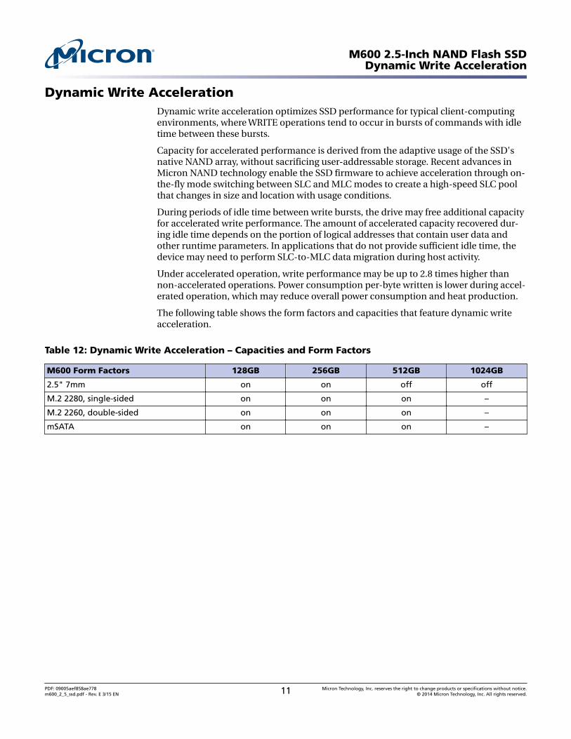
Dynamic Write AccelerationDynamic write acceleration optimizes SSD performance for typical client-computingenvironments, where WRITE operations tend to occur in bursts of commands with idletime between these bursts.
Capacity for accelerated performance is derived from the adaptive usage of the SSD'snative NAND array, without sacrificing user-addressable storage. Recent advances inMicron NAND technology enable the SSD firmware to achieve acceleration through on-the-fly mode switching between SLC and MLC modes to create a high-speed SLC poolthat changes in size and location with usage conditions.
During periods of idle time between write bursts, the drive may free additional capacityfor accelerated write performance. The amount of accelerated capacity recovered dur-ing idle time depends on the portion of logical addresses that contain user data andother runtime parameters. In applications that do not provide sufficient idle time, thedevice may need to perform SLC-to-MLC data migration during host activity.
Under accelerated operation, write performance may be up to 2.8 times higher thannon-accelerated operations. Power consumption per-byte written is lower during accel-erated operation, which may reduce overall power consumption and heat production.
The following table shows the form factors and capacities that feature dynamic writeacceleration.
Table 12: Dynamic Write Acceleration – Capacities and Form Factors
M600 Form Factors 128GB 256GB 512GB 1024GB
2.5" 7mm on on off off
M.2 2280, single-sided on on on –
M.2 2260, double-sided on on on –
mSATA on on on –
M600 2.5-Inch NAND Flash SSDDynamic Write Acceleration
PDF: 09005aef858ae778m600_2_5_ssd.pdf - Rev. E 3/15 EN 11 Micron Technology, Inc. reserves the right to change products or specifications without notice.
© 2014 Micron Technology, Inc. All rights reserved.
Adaptive Thermal MonitoringThe device features adaptive thermal monitoring. While most host computers exhibitoperating environments that keep an SSD running in the range of 40°C to 45°C, adap-tive thermal monitoring enables the SSD device to operate in a wide variety of environ-ments by helping to prevent the host computer from running at excessive temperatures.
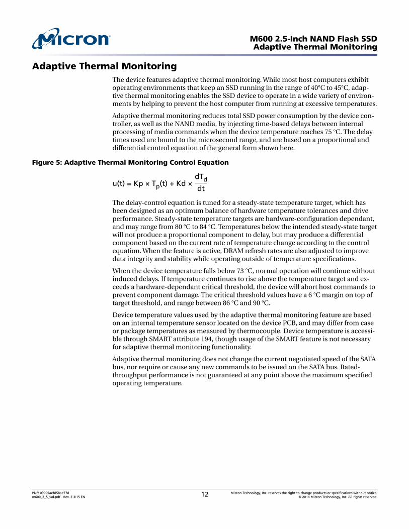
Adaptive thermal monitoring reduces total SSD power consumption by the device con-troller, as well as the NAND media, by injecting time-based delays between internalprocessing of media commands when the device temperature reaches 75 °C. The delaytimes used are bound to the microsecond range, and are based on a proportional anddifferential control equation of the general form shown here.
Figure 5: Adaptive Thermal Monitoring Control Equation
u(t) = Kp × Tp(t) + Kd × dTd
dt
The delay-control equation is tuned for a steady-state temperature target, which hasbeen designed as an optimum balance of hardware temperature tolerances and driveperformance. Steady-state temperature targets are hardware-configuration dependant,and may range from 80 °C to 84 °C. Temperatures below the intended steady-state targetwill not produce a proportional component to delay, but may produce a differentialcomponent based on the current rate of temperature change according to the controlequation. When the feature is active, DRAM refresh rates are also adjusted to improvedata integrity and stability while operating outside of temperature specifications.
When the device temperature falls below 73 °C, normal operation will continue withoutinduced delays. If temperature continues to rise above the temperature target and ex-ceeds a hardware-dependant critical threshold, the device will abort host commands toprevent component damage. The critical threshold values have a 6 °C margin on top oftarget threshold, and range between 86 °C and 90 °C.
Device temperature values used by the adaptive thermal monitoring feature are basedon an internal temperature sensor located on the device PCB, and may differ from caseor package temperatures as measured by thermocouple. Device temperature is accessi-ble through SMART attribute 194, though usage of the SMART feature is not necessaryfor adaptive thermal monitoring functionality.
Adaptive thermal monitoring does not change the current negotiated speed of the SATAbus, nor require or cause any new commands to be issued on the SATA bus. Rated-throughput performance is not guaranteed at any point above the maximum specifiedoperating temperature.
M600 2.5-Inch NAND Flash SSDAdaptive Thermal Monitoring
PDF: 09005aef858ae778m600_2_5_ssd.pdf - Rev. E 3/15 EN 12 Micron Technology, Inc. reserves the right to change products or specifications without notice.
© 2014 Micron Technology, Inc. All rights reserved.
TCG/Opal Support
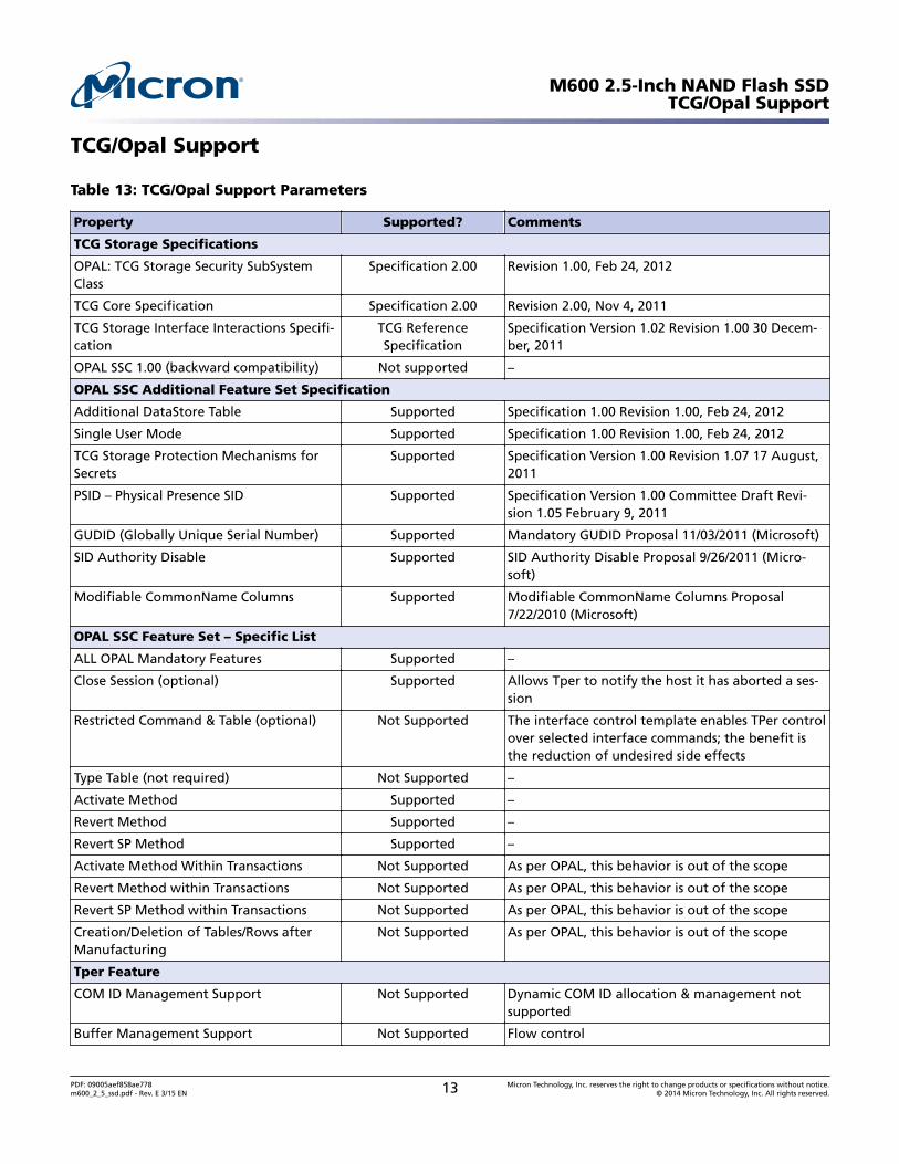
Table 13: TCG/Opal Support Parameters
Property Supported? Comments
TCG Storage Specifications
OPAL: TCG Storage Security SubSystemClass
Specification 2.00 Revision 1.00, Feb 24, 2012
TCG Core Specification Specification 2.00 Revision 2.00, Nov 4, 2011
TCG Storage Interface Interactions Specifi-cation
TCG ReferenceSpecification
Specification Version 1.02 Revision 1.00 30 Decem-ber, 2011
OPAL SSC 1.00 (backward compatibility) Not supported –
OPAL SSC Additional Feature Set Specification
Additional DataStore Table Supported Specification 1.00 Revision 1.00, Feb 24, 2012
Single User Mode Supported Specification 1.00 Revision 1.00, Feb 24, 2012
TCG Storage Protection Mechanisms forSecrets
Supported Specification Version 1.00 Revision 1.07 17 August,2011
PSID – Physical Presence SID Supported Specification Version 1.00 Committee Draft Revi-sion 1.05 February 9, 2011
GUDID (Globally Unique Serial Number) Supported Mandatory GUDID Proposal 11/03/2011 (Microsoft)
SID Authority Disable Supported SID Authority Disable Proposal 9/26/2011 (Micro-soft)
Modifiable CommonName Columns Supported Modifiable CommonName Columns Proposal7/22/2010 (Microsoft)
OPAL SSC Feature Set – Specific List
ALL OPAL Mandatory Features Supported –
Close Session (optional) Supported Allows Tper to notify the host it has aborted a ses-sion
Restricted Command & Table (optional) Not Supported The interface control template enables TPer controlover selected interface commands; the benefit isthe reduction of undesired side effects
Type Table (not required) Not Supported –
Activate Method Supported –
Revert Method Supported –
Revert SP Method Supported –
Activate Method Within Transactions Not Supported As per OPAL, this behavior is out of the scope
Revert Method within Transactions Not Supported As per OPAL, this behavior is out of the scope
Revert SP Method within Transactions Not Supported As per OPAL, this behavior is out of the scope
Creation/Deletion of Tables/Rows afterManufacturing
Not Supported As per OPAL, this behavior is out of the scope
Tper Feature
COM ID Management Support Not Supported Dynamic COM ID allocation & management notsupported
Buffer Management Support Not Supported Flow control
M600 2.5-Inch NAND Flash SSDTCG/Opal Support
PDF: 09005aef858ae778m600_2_5_ssd.pdf - Rev. E 3/15 EN 13 Micron Technology, Inc. reserves the right to change products or specifications without notice.
© 2014 Micron Technology, Inc. All rights reserved.
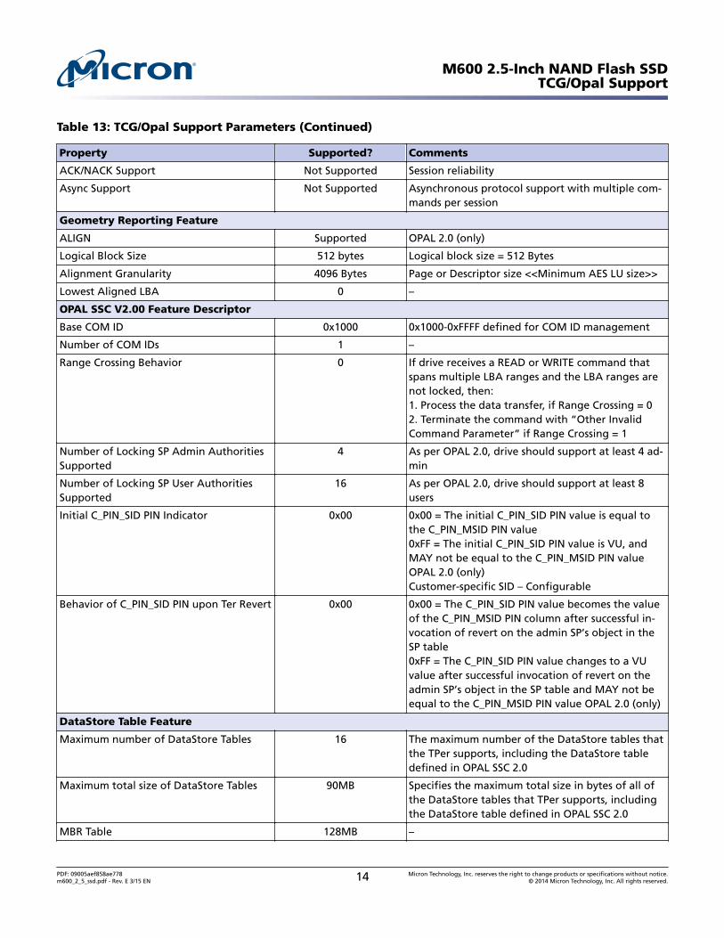
Table 13: TCG/Opal Support Parameters (Continued)
Property Supported? Comments
ACK/NACK Support Not Supported Session reliability
Async Support Not Supported Asynchronous protocol support with multiple com-mands per session
Geometry Reporting Feature
ALIGN Supported OPAL 2.0 (only)
Logical Block Size 512 bytes Logical block size = 512 Bytes
Alignment Granularity 4096 Bytes Page or Descriptor size <<Minimum AES LU size>>
Lowest Aligned LBA 0 –
OPAL SSC V2.00 Feature Descriptor
Base COM ID 0x1000 0x1000-0xFFFF defined for COM ID management
Number of COM IDs 1 –
Range Crossing Behavior 0 If drive receives a READ or WRITE command thatspans multiple LBA ranges and the LBA ranges arenot locked, then:1. Process the data transfer, if Range Crossing = 02. Terminate the command with “Other InvalidCommand Parameter” if Range Crossing = 1
Number of Locking SP Admin AuthoritiesSupported
4 As per OPAL 2.0, drive should support at least 4 ad-min
Number of Locking SP User AuthoritiesSupported
16 As per OPAL 2.0, drive should support at least 8users
Initial C_PIN_SID PIN Indicator 0x00 0x00 = The initial C_PIN_SID PIN value is equal tothe C_PIN_MSID PIN value0xFF = The initial C_PIN_SID PIN value is VU, andMAY not be equal to the C_PIN_MSID PIN valueOPAL 2.0 (only)Customer-specific SID – Configurable
Behavior of C_PIN_SID PIN upon Ter Revert 0x00 0x00 = The C_PIN_SID PIN value becomes the valueof the C_PIN_MSID PIN column after successful in-vocation of revert on the admin SP’s object in theSP table0xFF = The C_PIN_SID PIN value changes to a VUvalue after successful invocation of revert on theadmin SP’s object in the SP table and MAY not beequal to the C_PIN_MSID PIN value OPAL 2.0 (only)
DataStore Table Feature
Maximum number of DataStore Tables 16 The maximum number of the DataStore tables thatthe TPer supports, including the DataStore tabledefined in OPAL SSC 2.0
Maximum total size of DataStore Tables 90MB Specifies the maximum total size in bytes of all ofthe DataStore tables that TPer supports, includingthe DataStore table defined in OPAL SSC 2.0
MBR Table 128MB –
M600 2.5-Inch NAND Flash SSDTCG/Opal Support
PDF: 09005aef858ae778m600_2_5_ssd.pdf - Rev. E 3/15 EN 14 Micron Technology, Inc. reserves the right to change products or specifications without notice.
© 2014 Micron Technology, Inc. All rights reserved.

Table 13: TCG/Opal Support Parameters (Continued)
Property Supported? Comments
Byte Table Access Granularity
Mandatory Write Granularity 1 TPer enforces when the host invokes the set meth-od on byte tables; it should be less than or equal to8192; it should be less than or equal to Recommen-ded Access Granularity, OPAL 2.0 (only)
Recommended Access Granularity 8192 Tper recommends when the host invokes the set orget method on byte tables; it should be less than orequal to 8192
Cryptographic Features
AES Key Size 256 Bits AES key is generated by using CTR DRBG algorithm(FIPS Compliant)
AES Mode CBC IV swapped
Number of Ranges/Band Supported 16(15 user definable,
1 global range)
Now supporting 15 LBA ranges; range cross readand write allowed if LBA ranges are unlocked
Re-Encryption Not Supported –
Key Management Cryptographic
Crypto Erase Completion Time <1s Yes –
Cryptographic Algorithms are Certified byFIPS-197
No Designed to meet, no plans for certification
AES 256-Bit CBC/ECB Mode Supported ECB mode used only for generating the randomkey by CTR DRBG
CTR DRBG Supported –
SHA 256 Supported –
RSA 2048 Signature Verification Supported –
TPer Communication Properties
Max ComPacket Size 131072 256 sectors (128K)
Max Response ComPacket Size 131072 256 sectors (128K)
Max Packet Size 128512 –
Max Individual Token Size 123904 –
Max Packets 1 –
Max SubPackets 1 –
Max Sessions 1 Each session requires a set of buffers and variables
Max Transaction Limit 1 Transaction are inside sessions
Max Methods 1 Methods are contained in a transaction
Max Authentications 14 –
Def Session Timeout Yes The session timeout length (in milliseconds) usedby the TPer by default
IEEE1667
Probe Silo Supported –
M600 2.5-Inch NAND Flash SSDTCG/Opal Support
PDF: 09005aef858ae778m600_2_5_ssd.pdf - Rev. E 3/15 EN 15 Micron Technology, Inc. reserves the right to change products or specifications without notice.
© 2014 Micron Technology, Inc. All rights reserved.
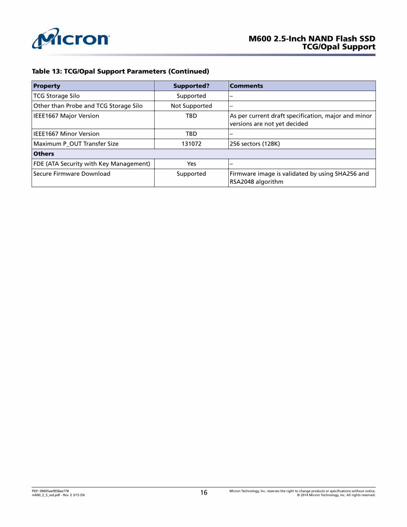
Table 13: TCG/Opal Support Parameters (Continued)
Property Supported? Comments
TCG Storage Silo Supported –
Other than Probe and TCG Storage Silo Not Supported –
IEEE1667 Major Version TBD As per current draft specification, major and minorversions are not yet decided
IEEE1667 Minor Version TBD –
Maximum P_OUT Transfer Size 131072 256 sectors (128K)
Others
FDE (ATA Security with Key Management) Yes –
Secure Firmware Download Supported Firmware image is validated by using SHA256 andRSA2048 algorithm
M600 2.5-Inch NAND Flash SSDTCG/Opal Support
PDF: 09005aef858ae778m600_2_5_ssd.pdf - Rev. E 3/15 EN 16 Micron Technology, Inc. reserves the right to change products or specifications without notice.
© 2014 Micron Technology, Inc. All rights reserved.
Device ID
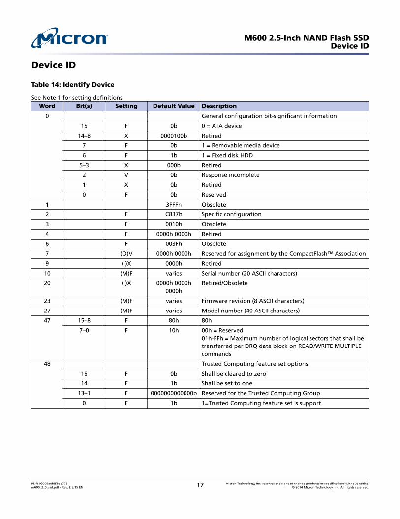
Table 14: Identify Device
See Note 1 for setting definitionsWord Bit(s) Setting Default Value Description
0 General configuration bit-significant information
15 F 0b 0 = ATA device
14–8 X 0000100b Retired
7 F 0b 1 = Removable media device
6 F 1b 1 = Fixed disk HDD
5–3 X 000b Retired
2 V 0b Response incomplete
1 X 0b Retired
0 F 0b Reserved
1 3FFFh Obsolete
2 F C837h Specific configuration
3 F 0010h Obsolete
4 F 0000h 0000h Retired
6 F 003Fh Obsolete
7 (O)V 0000h 0000h Reserved for assignment by the CompactFlash™ Association
9 ( )X 0000h Retired
10 (M)F varies Serial number (20 ASCII characters)
20 ( )X 0000h 0000h0000h
Retired/Obsolete
23 (M)F varies Firmware revision (8 ASCII characters)
27 (M)F varies Model number (40 ASCII characters)
47 15–8 F 80h 80h
7–0 F 10h 00h = Reserved01h-FFh = Maximum number of logical sectors that shall betransferred per DRQ data block on READ/WRITE MULTIPLEcommands
48 Trusted Computing feature set options
15 F 0b Shall be cleared to zero
14 F 1b Shall be set to one
13–1 F 0000000000000b Reserved for the Trusted Computing Group
0 F 1b 1=Trusted Computing feature set is support
M600 2.5-Inch NAND Flash SSDDevice ID
PDF: 09005aef858ae778m600_2_5_ssd.pdf - Rev. E 3/15 EN 17 Micron Technology, Inc. reserves the right to change products or specifications without notice.
© 2014 Micron Technology, Inc. All rights reserved.
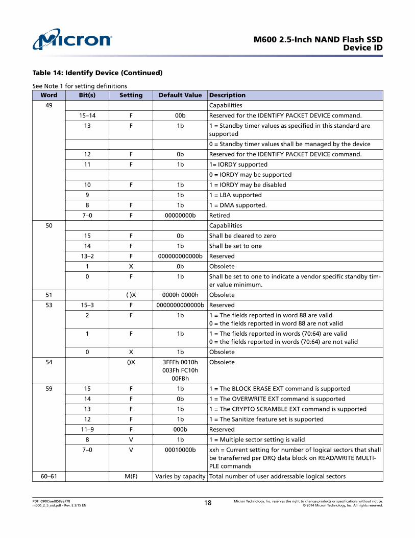
Table 14: Identify Device (Continued)
See Note 1 for setting definitionsWord Bit(s) Setting Default Value Description
49 Capabilities
15–14 F 00b Reserved for the IDENTIFY PACKET DEVICE command.
13 F 1b 1 = Standby timer values as specified in this standard aresupported
0 = Standby timer values shall be managed by the device
12 F 0b Reserved for the IDENTIFY PACKET DEVICE command.
11 F 1b 1= IORDY supported
0 = IORDY may be supported
10 F 1b 1 = IORDY may be disabled
9 1b 1 = LBA supported
8 F 1b 1 = DMA supported.
7–0 F 00000000b Retired
50 Capabilities
15 F 0b Shall be cleared to zero
14 F 1b Shall be set to one
13–2 F 000000000000b Reserved
1 X 0b Obsolete
0 F 1b Shall be set to one to indicate a vendor specific standby tim-er value minimum.
51 ( )X 0000h 0000h Obsolete
53 15–3 F 0000000000000b Reserved
2 F 1b 1 = The fields reported in word 88 are valid0 = the fields reported in word 88 are not valid
1 F 1b 1 = The fields reported in words (70:64) are valid0 = the fields reported in words (70:64) are not valid
0 X 1b Obsolete
54 ()X 3FFFh 0010h003Fh FC10h
00FBh
Obsolete
59 15 F 1b 1 = The BLOCK ERASE EXT command is supported
14 F 0b 1 = The OVERWRITE EXT command is supported
13 F 1b 1 = The CRYPTO SCRAMBLE EXT command is supported
12 F 1b 1 = The Sanitize feature set is supported
11–9 F 000b Reserved
8 V 1b 1 = Multiple sector setting is valid
7–0 V 00010000b xxh = Current setting for number of logical sectors that shallbe transferred per DRQ data block on READ/WRITE MULTI-PLE commands
60–61 M(F) Varies by capacity Total number of user addressable logical sectors
M600 2.5-Inch NAND Flash SSDDevice ID
PDF: 09005aef858ae778m600_2_5_ssd.pdf - Rev. E 3/15 EN 18 Micron Technology, Inc. reserves the right to change products or specifications without notice.
© 2014 Micron Technology, Inc. All rights reserved.
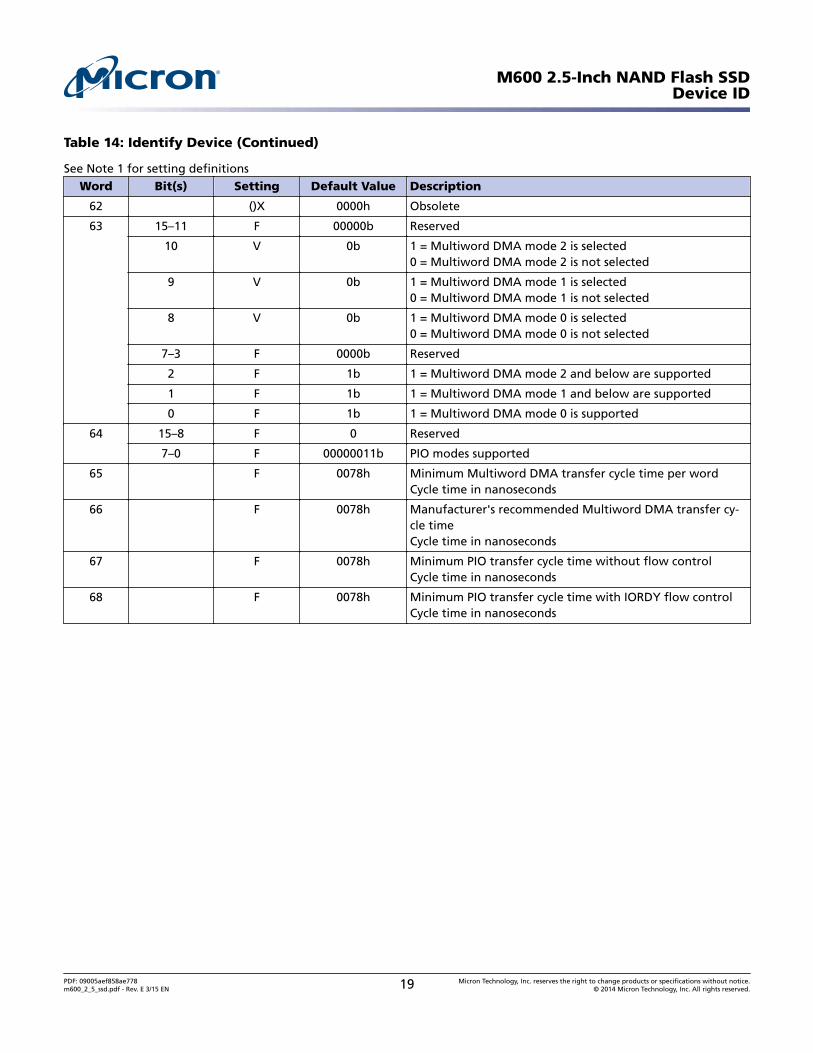
Table 14: Identify Device (Continued)
See Note 1 for setting definitionsWord Bit(s) Setting Default Value Description
62 ()X 0000h Obsolete
63 15–11 F 00000b Reserved
10 V 0b 1 = Multiword DMA mode 2 is selected0 = Multiword DMA mode 2 is not selected
9 V 0b 1 = Multiword DMA mode 1 is selected0 = Multiword DMA mode 1 is not selected
8 V 0b 1 = Multiword DMA mode 0 is selected0 = Multiword DMA mode 0 is not selected
7–3 F 0000b Reserved
2 F 1b 1 = Multiword DMA mode 2 and below are supported
1 F 1b 1 = Multiword DMA mode 1 and below are supported
0 F 1b 1 = Multiword DMA mode 0 is supported
64 15–8 F 0 Reserved
7–0 F 00000011b PIO modes supported
65 F 0078h Minimum Multiword DMA transfer cycle time per wordCycle time in nanoseconds
66 F 0078h Manufacturer's recommended Multiword DMA transfer cy-cle timeCycle time in nanoseconds
67 F 0078h Minimum PIO transfer cycle time without flow controlCycle time in nanoseconds
68 F 0078h Minimum PIO transfer cycle time with IORDY flow controlCycle time in nanoseconds
M600 2.5-Inch NAND Flash SSDDevice ID
PDF: 09005aef858ae778m600_2_5_ssd.pdf - Rev. E 3/15 EN 19 Micron Technology, Inc. reserves the right to change products or specifications without notice.
© 2014 Micron Technology, Inc. All rights reserved.
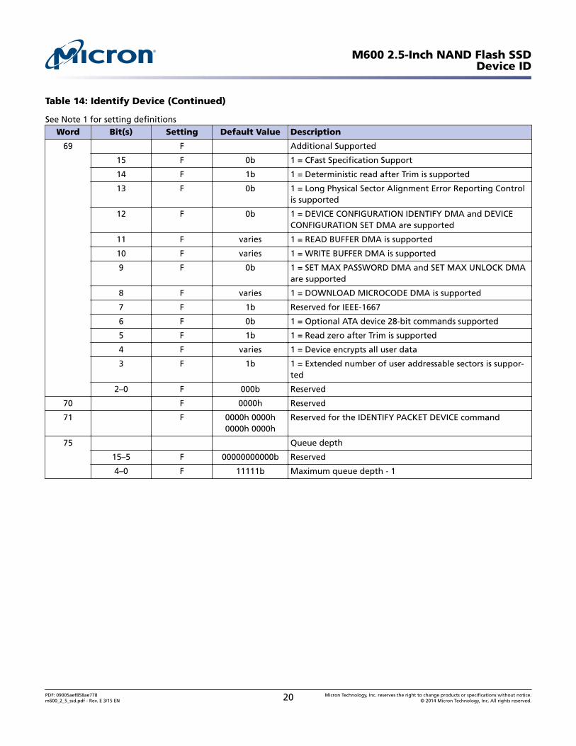
Table 14: Identify Device (Continued)
See Note 1 for setting definitionsWord Bit(s) Setting Default Value Description
69 F Additional Supported
15 F 0b 1 = CFast Specification Support
14 F 1b 1 = Deterministic read after Trim is supported
13 F 0b 1 = Long Physical Sector Alignment Error Reporting Controlis supported
12 F 0b 1 = DEVICE CONFIGURATION IDENTIFY DMA and DEVICECONFIGURATION SET DMA are supported
11 F varies 1 = READ BUFFER DMA is supported
10 F varies 1 = WRITE BUFFER DMA is supported
9 F 0b 1 = SET MAX PASSWORD DMA and SET MAX UNLOCK DMAare supported
8 F varies 1 = DOWNLOAD MICROCODE DMA is supported
7 F 1b Reserved for IEEE-1667
6 F 0b 1 = Optional ATA device 28-bit commands supported
5 F 1b 1 = Read zero after Trim is supported
4 F varies 1 = Device encrypts all user data
3 F 1b 1 = Extended number of user addressable sectors is suppor-ted
2–0 F 000b Reserved
70 F 0000h Reserved
71 F 0000h 0000h0000h 0000h
Reserved for the IDENTIFY PACKET DEVICE command
75 Queue depth
15–5 F 00000000000b Reserved
4–0 F 11111b Maximum queue depth - 1
M600 2.5-Inch NAND Flash SSDDevice ID
PDF: 09005aef858ae778m600_2_5_ssd.pdf - Rev. E 3/15 EN 20 Micron Technology, Inc. reserves the right to change products or specifications without notice.
© 2014 Micron Technology, Inc. All rights reserved.

Table 14: Identify Device (Continued)
See Note 1 for setting definitionsWord Bit(s) Setting Default Value Description
76 Serial ATA capabilities
15 F 1b 1 = Supports READ LOG DMA EXT as equivalent to READLOG EXT
14 F 0b 1 = Supports device automatic partial to slumber transitions
13 F 0b 1 = Supports host automatic partial to slumber transitions
12 F 1b Supports Native Command Queuing priority information
11 F 0b Supports Unload while NCQ commands outstanding
10 F 1b Supports Phy event counters
9 F 0b Supports receipt of host initiated interface power manage-ment requests
8 F 1b Supports native Command Queueing
7–4 F 0000b Reserved for future Serial ATA signaling speed grades
3 F 1b 1 = Supports Serial ATA Gen-3 speed (6.0 Gb/s)
2 F 1b 1 = Supports Serial ATA Gen-2 speed (3.0 Gb/s)
1 F 1b 1 = Supports Serial ATA Gen-1 speed (1.5 Gb/s)
0 F 0b Reserved (set to 0)
77 Serial ATA additional capabilities
15–8 F 00000000b Reserved for future Serial ATA definition
7 F 1b 1 = Supports DEVSLP_to_ReducedPwrState
6 F 1b Supports RECEIVE FPDMA QUEUED and SEND FPDMAQUEUED commands
5 F 0b Supports NCQ Queue Management Command
4 F 0b Supports NCQ Streaming
3–1 V varies Coded value indicating current negotiated Serial ATA signalspeed
0 F 0b Shall be cleared to zero
78 Serial ATA features supported
15–9 F 0000000b Reserved
8 F 1b 1 = Device sleep supported
7 F 0b 1 = Supports NCQ Autosense
6 F 1b 1 = Supports software settings preservation
5 F 1b 1 = HARDWARE FEATURE CONTROL SUPPORTED bit
4 F 0b 1 = Supports in-order data delivery
3 F 1b 1 = Supports dev initiate interface power management
2 F 1b 1 = Supports DMA Setup Auto-Activate optimization
1 F 0b 1 = Supports non-zero buffer offsets in DMA Setup FIS
0 F 0b Reserved (set to 0)
M600 2.5-Inch NAND Flash SSDDevice ID
PDF: 09005aef858ae778m600_2_5_ssd.pdf - Rev. E 3/15 EN 21 Micron Technology, Inc. reserves the right to change products or specifications without notice.
© 2014 Micron Technology, Inc. All rights reserved.
Table 14: Identify Device (Continued)
See Note 1 for setting definitionsWord Bit(s) Setting Default Value Description
79 Serial ATA features enabled
15–9 V 0000000b Reserved
8 V 0b 1 = Device sleep enabled
7 V 1b 1 = Automatic partial to slumber transitions enabled
6 V 1b 1 = Software settings preservation enabled
5 V 0b 1 = Hardware feature control is enabled
4 V 0b 1 = In-order data delivery enabled
3 V 0b 1 = Device initiating interface power management enabled
2 V 0b 1 = DMA Setup Auto-Activate optimization enabled
1 V 0b 1 = Non-zero buffer offsets in DMA Setup FIS enabled
0 V 0b Reserved (set to 0)
80 Major revision number
15–11 F 00000b Reserved
10 F 1b 1 = Supports ACS-3
9 F 1b 1 = Supports ATA8-ACS2
8 F 1b 1 = Supports ATA8-ACS
7 F 1b 1 = Supports ATA/ATAPI-7
6 F 1b 1 = Supports ATA/ATAPI-6
5 F 1b 1 = Supports ATA/ATAPI-5
4 F 1b 1 = Supports ATA/ATAPI-4
3 F 1b Obsolete
2 S 0b Obsolete
1 S 0b Obsolete
0 F 0b Reserved
81 F 011Bh Minor revision number
011Bh = ACS-3 version 4
M600 2.5-Inch NAND Flash SSDDevice ID
PDF: 09005aef858ae778m600_2_5_ssd.pdf - Rev. E 3/15 EN 22 Micron Technology, Inc. reserves the right to change products or specifications without notice.
© 2014 Micron Technology, Inc. All rights reserved.
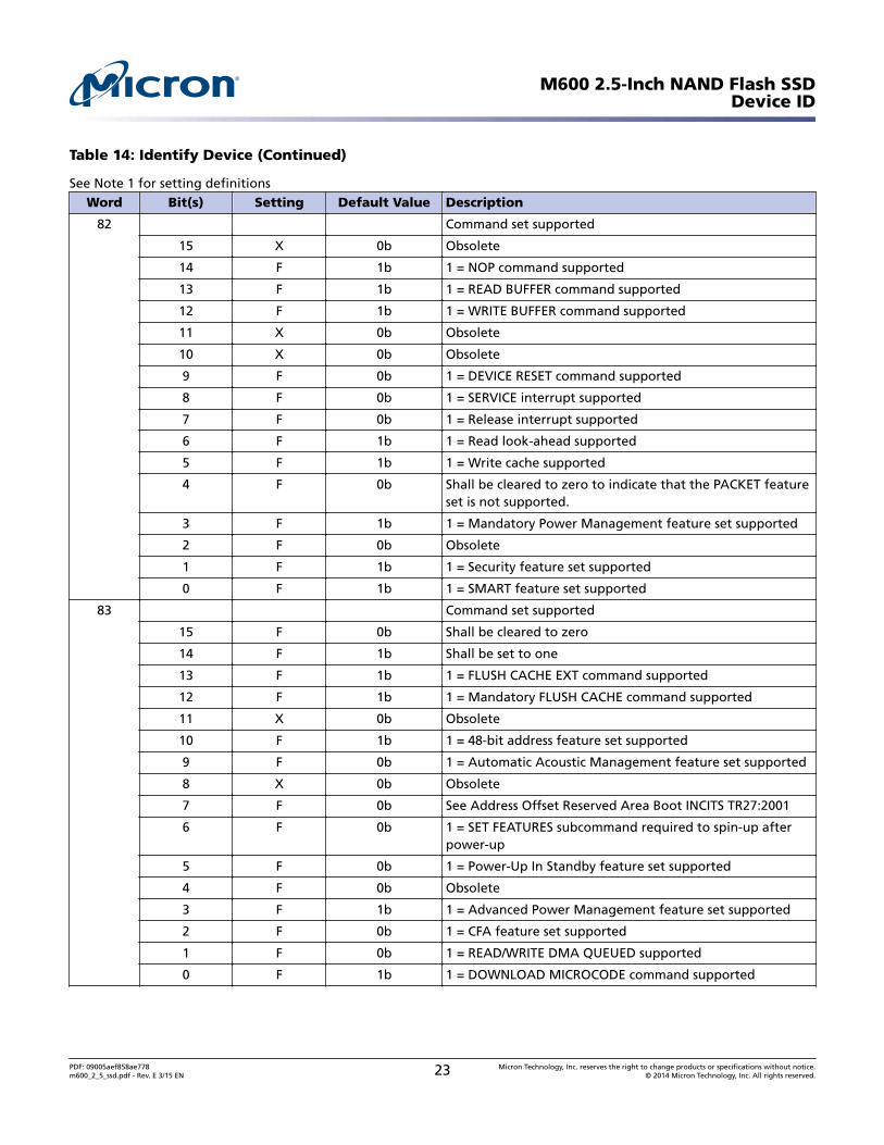
Table 14: Identify Device (Continued)
See Note 1 for setting definitionsWord Bit(s) Setting Default Value Description
82 Command set supported
15 X 0b Obsolete
14 F 1b 1 = NOP command supported
13 F 1b 1 = READ BUFFER command supported
12 F 1b 1 = WRITE BUFFER command supported
11 X 0b Obsolete
10 X 0b Obsolete
9 F 0b 1 = DEVICE RESET command supported
8 F 0b 1 = SERVICE interrupt supported
7 F 0b 1 = Release interrupt supported
6 F 1b 1 = Read look-ahead supported
5 F 1b 1 = Write cache supported
4 F 0b Shall be cleared to zero to indicate that the PACKET featureset is not supported.
3 F 1b 1 = Mandatory Power Management feature set supported
2 F 0b Obsolete
1 F 1b 1 = Security feature set supported
0 F 1b 1 = SMART feature set supported
83 Command set supported
15 F 0b Shall be cleared to zero
14 F 1b Shall be set to one
13 F 1b 1 = FLUSH CACHE EXT command supported
12 F 1b 1 = Mandatory FLUSH CACHE command supported
11 X 0b Obsolete
10 F 1b 1 = 48-bit address feature set supported
9 F 0b 1 = Automatic Acoustic Management feature set supported
8 X 0b Obsolete
7 F 0b See Address Offset Reserved Area Boot INCITS TR27:2001
6 F 0b 1 = SET FEATURES subcommand required to spin-up afterpower-up
5 F 0b 1 = Power-Up In Standby feature set supported
4 F 0b Obsolete
3 F 1b 1 = Advanced Power Management feature set supported
2 F 0b 1 = CFA feature set supported
1 F 0b 1 = READ/WRITE DMA QUEUED supported
0 F 1b 1 = DOWNLOAD MICROCODE command supported
M600 2.5-Inch NAND Flash SSDDevice ID
PDF: 09005aef858ae778m600_2_5_ssd.pdf - Rev. E 3/15 EN 23 Micron Technology, Inc. reserves the right to change products or specifications without notice.
© 2014 Micron Technology, Inc. All rights reserved.

Table 14: Identify Device (Continued)
See Note 1 for setting definitionsWord Bit(s) Setting Default Value Description
84 Command set/feature supported extension
15 F 0b Shall be cleared to zero
14 F 1b Shall be set to one
13 F 1b 1 = IDLE IMMEDIATE with UNLOAD FEATURE supported
12 F 0b Reserved for technical report INCITS TR-37-2004 (TLC)
11 F 0b Reserved for technical report INCITS TR-37-2004 (TLC)
10–9 F 00b Obsolete
8 F 1b 1 = 64-bit word wide name supported
7 F 0b 1 = WRITE DMA QUEUED FUA EXT command supported
6 F 1b 1 = WRITE DMA FUA EXT and WRITE MULTIPLE FUA EXTcommands supported
5 F 1b 1 = General Purpose Logging feature set supported
4 F 0b 1 = Streaming feature set supported
3 F 0b 1 = Media Card Pass Through Command feature set suppor-ted
2 F 0b 1 = Media serial number supported
1 F 1b 1 = SMART self-test supported
0 F 1b 1 = SMART error logging supported
85 Command set/feature enabled.
15 X 0b Obsolete
14 F 1b 1 = NOP command supported
13 F 1b 1 = READ BUFFER command supported
12 F 1b 1 = WRITE BUFFER command supported
11 X 0b Obsolete
10 X 0b Obsolete
9 F 0b 1 = DEVICE RESET command supported
8 V 0b 1 = SERVICE interrupt enabled
7 V 0b 1 = Release interrupt enabled
6 V 1b 1 = Look-ahead enabled
5 V 1b 1 = Write cache enabled
4 F 0b Shall be cleared to zero to indicate that the PACKET featureset is not supported.
3 F 1b Power Management feature set is enabled
2 F 0b Obsolete
1 V 0b 1 = Security Mode feature set enabled
0 V 1b 1 = SMART feature set enabled
M600 2.5-Inch NAND Flash SSDDevice ID
PDF: 09005aef858ae778m600_2_5_ssd.pdf - Rev. E 3/15 EN 24 Micron Technology, Inc. reserves the right to change products or specifications without notice.
© 2014 Micron Technology, Inc. All rights reserved.
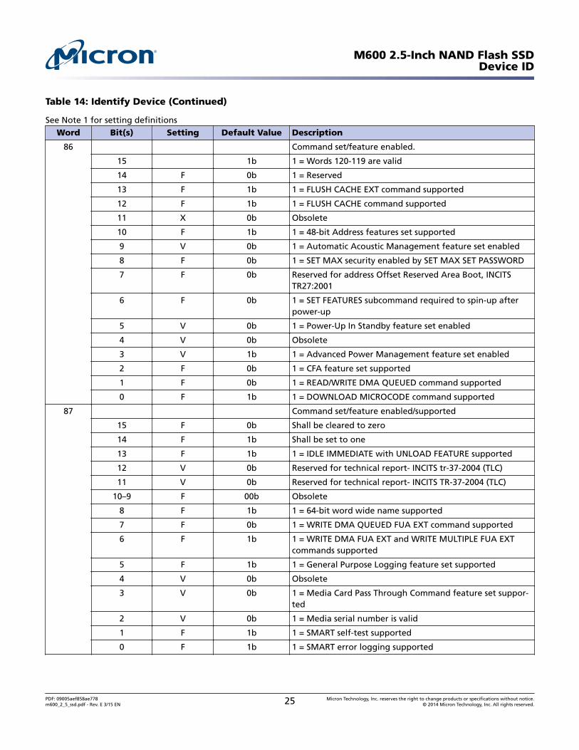
Table 14: Identify Device (Continued)
See Note 1 for setting definitionsWord Bit(s) Setting Default Value Description
86 Command set/feature enabled.
15 1b 1 = Words 120-119 are valid
14 F 0b 1 = Reserved
13 F 1b 1 = FLUSH CACHE EXT command supported
12 F 1b 1 = FLUSH CACHE command supported
11 X 0b Obsolete
10 F 1b 1 = 48-bit Address features set supported
9 V 0b 1 = Automatic Acoustic Management feature set enabled
8 F 0b 1 = SET MAX security enabled by SET MAX SET PASSWORD
7 F 0b Reserved for address Offset Reserved Area Boot, INCITSTR27:2001
6 F 0b 1 = SET FEATURES subcommand required to spin-up afterpower-up
5 V 0b 1 = Power-Up In Standby feature set enabled
4 V 0b Obsolete
3 V 1b 1 = Advanced Power Management feature set enabled
2 F 0b 1 = CFA feature set supported
1 F 0b 1 = READ/WRITE DMA QUEUED command supported
0 F 1b 1 = DOWNLOAD MICROCODE command supported
87 Command set/feature enabled/supported
15 F 0b Shall be cleared to zero
14 F 1b Shall be set to one
13 F 1b 1 = IDLE IMMEDIATE with UNLOAD FEATURE supported
12 V 0b Reserved for technical report- INCITS tr-37-2004 (TLC)
11 V 0b Reserved for technical report- INCITS TR-37-2004 (TLC)
10–9 F 00b Obsolete
8 F 1b 1 = 64-bit word wide name supported
7 F 0b 1 = WRITE DMA QUEUED FUA EXT command supported
6 F 1b 1 = WRITE DMA FUA EXT and WRITE MULTIPLE FUA EXTcommands supported
5 F 1b 1 = General Purpose Logging feature set supported
4 V 0b Obsolete
3 V 0b 1 = Media Card Pass Through Command feature set suppor-ted
2 V 0b 1 = Media serial number is valid
1 F 1b 1 = SMART self-test supported
0 F 1b 1 = SMART error logging supported
M600 2.5-Inch NAND Flash SSDDevice ID
PDF: 09005aef858ae778m600_2_5_ssd.pdf - Rev. E 3/15 EN 25 Micron Technology, Inc. reserves the right to change products or specifications without notice.
© 2014 Micron Technology, Inc. All rights reserved.
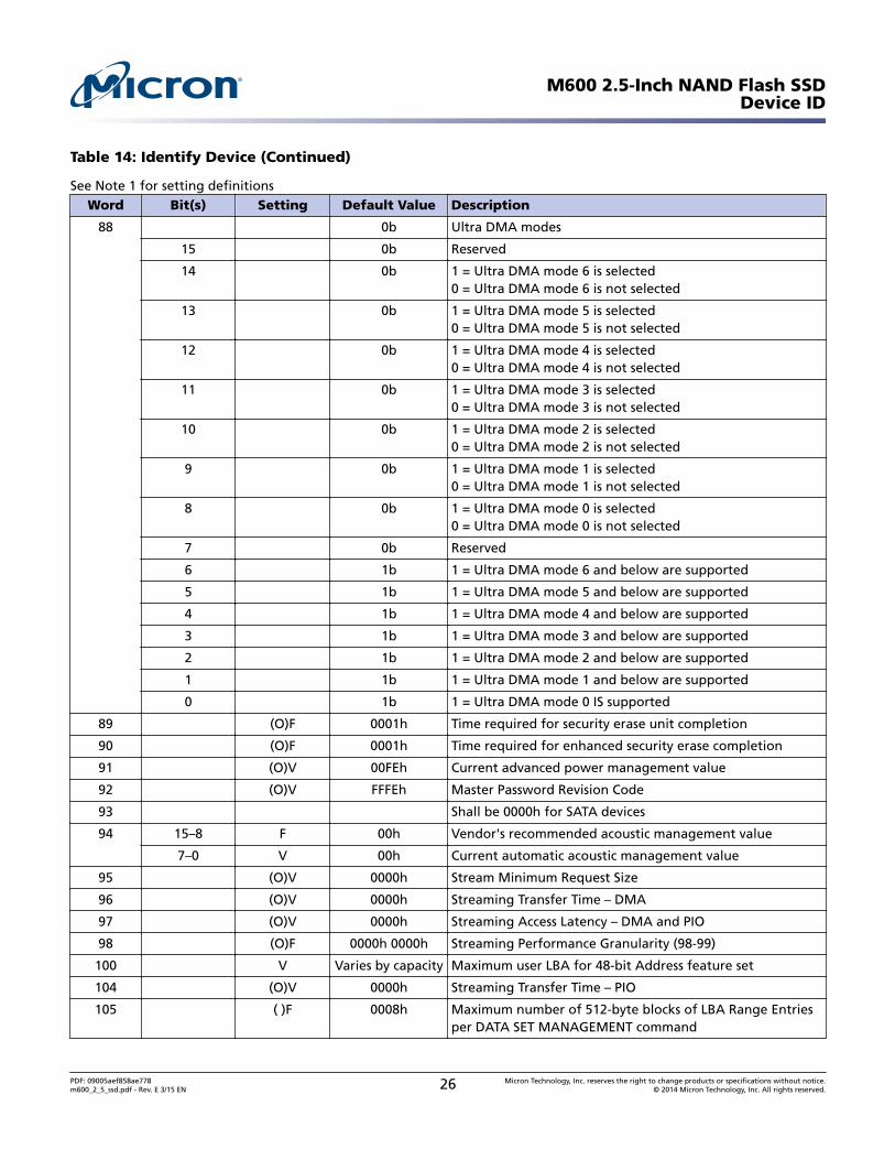
Table 14: Identify Device (Continued)
See Note 1 for setting definitionsWord Bit(s) Setting Default Value Description
88 0b Ultra DMA modes
15 0b Reserved
14 0b 1 = Ultra DMA mode 6 is selected0 = Ultra DMA mode 6 is not selected
13 0b 1 = Ultra DMA mode 5 is selected0 = Ultra DMA mode 5 is not selected
12 0b 1 = Ultra DMA mode 4 is selected0 = Ultra DMA mode 4 is not selected
11 0b 1 = Ultra DMA mode 3 is selected0 = Ultra DMA mode 3 is not selected
10 0b 1 = Ultra DMA mode 2 is selected0 = Ultra DMA mode 2 is not selected
9 0b 1 = Ultra DMA mode 1 is selected0 = Ultra DMA mode 1 is not selected
8 0b 1 = Ultra DMA mode 0 is selected0 = Ultra DMA mode 0 is not selected
7 0b Reserved
6 1b 1 = Ultra DMA mode 6 and below are supported
5 1b 1 = Ultra DMA mode 5 and below are supported
4 1b 1 = Ultra DMA mode 4 and below are supported
3 1b 1 = Ultra DMA mode 3 and below are supported
2 1b 1 = Ultra DMA mode 2 and below are supported
1 1b 1 = Ultra DMA mode 1 and below are supported
0 1b 1 = Ultra DMA mode 0 IS supported
89 (O)F 0001h Time required for security erase unit completion
90 (O)F 0001h Time required for enhanced security erase completion
91 (O)V 00FEh Current advanced power management value
92 (O)V FFFEh Master Password Revision Code
93 Shall be 0000h for SATA devices
94 15–8 F 00h Vendor's recommended acoustic management value
7–0 V 00h Current automatic acoustic management value
95 (O)V 0000h Stream Minimum Request Size
96 (O)V 0000h Streaming Transfer Time – DMA
97 (O)V 0000h Streaming Access Latency – DMA and PIO
98 (O)F 0000h 0000h Streaming Performance Granularity (98-99)
100 V Varies by capacity Maximum user LBA for 48-bit Address feature set
104 (O)V 0000h Streaming Transfer Time – PIO
105 ( )F 0008h Maximum number of 512-byte blocks of LBA Range Entriesper DATA SET MANAGEMENT command
M600 2.5-Inch NAND Flash SSDDevice ID
PDF: 09005aef858ae778m600_2_5_ssd.pdf - Rev. E 3/15 EN 26 Micron Technology, Inc. reserves the right to change products or specifications without notice.
© 2014 Micron Technology, Inc. All rights reserved.
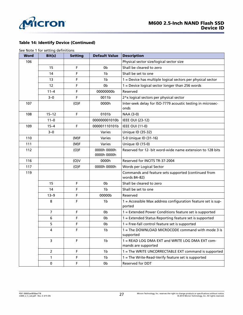
Table 14: Identify Device (Continued)
See Note 1 for setting definitionsWord Bit(s) Setting Default Value Description
106 Physical sector size/logical sector size
15 F 0b Shall be cleared to zero
14 F 1b Shall be set to one
13 F 1b 1 = Device has multiple logical sectors per physical sector
12 F 0b 1 = Device logical sector longer than 256 words
11–4 F 00000000b Reserved
3–0 F 0011b 2^x logical sectors per physical sector
107 (O)F 0000h Inter-seek delay for ISO-7779 acoustic testing in microsec-onds
108 15–12 F 0101b NAA (3-0)
11–0 000000001010b IEEE OUI (23-12)
109 15–4 F 000001110101b IEEE OUI (11-0)
3–0 Varies Unique ID (35-32)
110 (M)F Varies 5-0 Unique ID (31-16)
111 (M)F Varies Unique ID (15-0)
112 (O)F 0000h 0000h0000h 0000h
Reserved for 12- bit word-wide name extension to 128 bits
116 (O)V 0000h Reserved for INCITS TR-37-2004
117 (O)F 0000h 0000h Words per Logical Sector
119 Commands and feature sets supported (continued fromwords 84–82)
15 F 0b Shall be cleared to zero
14 F 1b Shall be set to one
13–9 F 00000b Reserved
8 F 1b 1 = Accessible Max address configuration feature set is sup-ported
7 F 0b 1 = Extended Power Conditions feature set is supported
6 F 0b 1 = Extended Status Reporting feature set is supported
5 F 0b 1 = Free-fall control feature set is supported
4 F 1b 1 = The DOWNLOAD MICROCODE command with mode 3 issupported
3 F 1b 1 = READ LOG DMA EXT and WRITE LOG DMA EXT com-mands are supported
2 F 1b 1 = The WRITE UNCORRECTABLE EXT command is supported
1 F 1b 1 = The Write-Read-Verify feature set is supported
0 F 0b Reserved for DDT
M600 2.5-Inch NAND Flash SSDDevice ID
PDF: 09005aef858ae778m600_2_5_ssd.pdf - Rev. E 3/15 EN 27 Micron Technology, Inc. reserves the right to change products or specifications without notice.
© 2014 Micron Technology, Inc. All rights reserved.
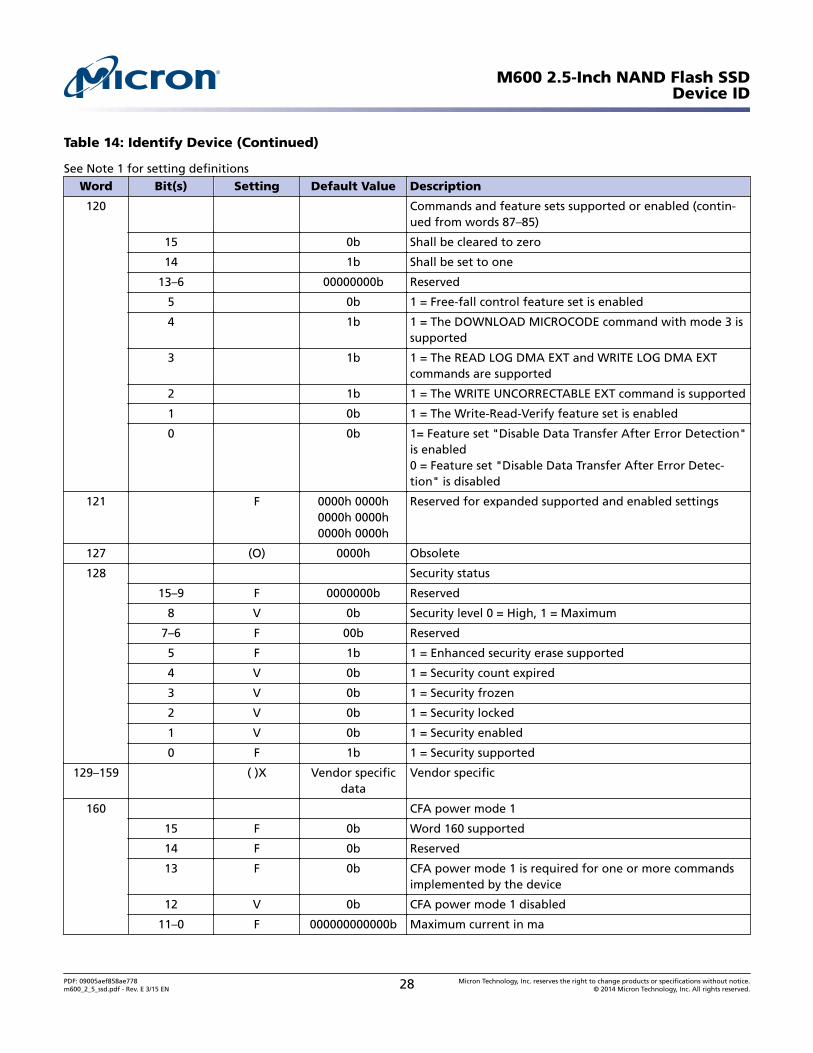
Table 14: Identify Device (Continued)
See Note 1 for setting definitionsWord Bit(s) Setting Default Value Description
120 Commands and feature sets supported or enabled (contin-ued from words 87–85)
15 0b Shall be cleared to zero
14 1b Shall be set to one
13–6 00000000b Reserved
5 0b 1 = Free-fall control feature set is enabled
4 1b 1 = The DOWNLOAD MICROCODE command with mode 3 issupported
3 1b 1 = The READ LOG DMA EXT and WRITE LOG DMA EXTcommands are supported
2 1b 1 = The WRITE UNCORRECTABLE EXT command is supported
1 0b 1 = The Write-Read-Verify feature set is enabled
0 0b 1= Feature set "Disable Data Transfer After Error Detection"is enabled0 = Feature set "Disable Data Transfer After Error Detec-tion" is disabled
121 F 0000h 0000h0000h 0000h0000h 0000h
Reserved for expanded supported and enabled settings
127 (O) 0000h Obsolete
128 Security status
15–9 F 0000000b Reserved
8 V 0b Security level 0 = High, 1 = Maximum
7–6 F 00b Reserved
5 F 1b 1 = Enhanced security erase supported
4 V 0b 1 = Security count expired
3 V 0b 1 = Security frozen
2 V 0b 1 = Security locked
1 V 0b 1 = Security enabled
0 F 1b 1 = Security supported
129–159 ( )X Vendor specificdata
Vendor specific
160 CFA power mode 1
15 F 0b Word 160 supported
14 F 0b Reserved
13 F 0b CFA power mode 1 is required for one or more commandsimplemented by the device
12 V 0b CFA power mode 1 disabled
11–0 F 000000000000b Maximum current in ma
M600 2.5-Inch NAND Flash SSDDevice ID
PDF: 09005aef858ae778m600_2_5_ssd.pdf - Rev. E 3/15 EN 28 Micron Technology, Inc. reserves the right to change products or specifications without notice.
© 2014 Micron Technology, Inc. All rights reserved.
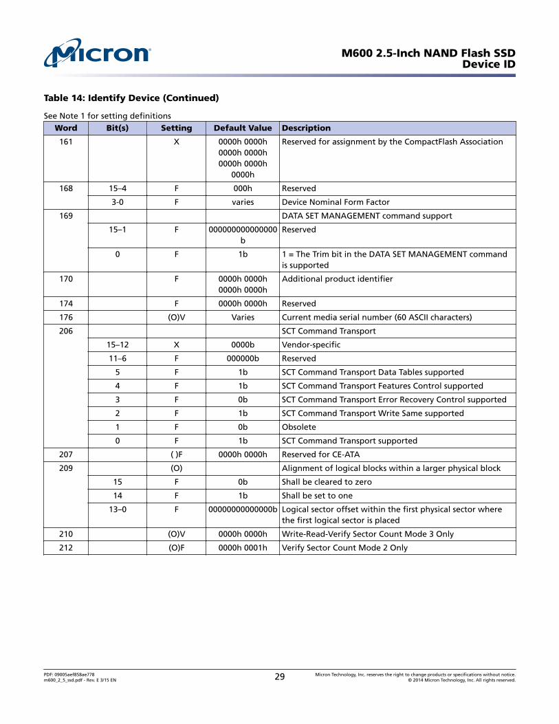
Table 14: Identify Device (Continued)
See Note 1 for setting definitionsWord Bit(s) Setting Default Value Description
161 X 0000h 0000h0000h 0000h0000h 0000h
0000h
Reserved for assignment by the CompactFlash Association
168 15–4 F 000h Reserved
3-0 F varies Device Nominal Form Factor
169 DATA SET MANAGEMENT command support
15–1 F 000000000000000b
Reserved
0 F 1b 1 = The Trim bit in the DATA SET MANAGEMENT commandis supported
170 F 0000h 0000h0000h 0000h
Additional product identifier
174 F 0000h 0000h Reserved
176 (O)V Varies Current media serial number (60 ASCII characters)
206 SCT Command Transport
15–12 X 0000b Vendor-specific
11–6 F 000000b Reserved
5 F 1b SCT Command Transport Data Tables supported
4 F 1b SCT Command Transport Features Control supported
3 F 0b SCT Command Transport Error Recovery Control supported
2 F 1b SCT Command Transport Write Same supported
1 F 0b Obsolete
0 F 1b SCT Command Transport supported
207 ( )F 0000h 0000h Reserved for CE-ATA
209 (O) Alignment of logical blocks within a larger physical block
15 F 0b Shall be cleared to zero
14 F 1b Shall be set to one
13–0 F 00000000000000b Logical sector offset within the first physical sector wherethe first logical sector is placed
210 (O)V 0000h 0000h Write-Read-Verify Sector Count Mode 3 Only
212 (O)F 0000h 0001h Verify Sector Count Mode 2 Only
M600 2.5-Inch NAND Flash SSDDevice ID
PDF: 09005aef858ae778m600_2_5_ssd.pdf - Rev. E 3/15 EN 29 Micron Technology, Inc. reserves the right to change products or specifications without notice.
© 2014 Micron Technology, Inc. All rights reserved.
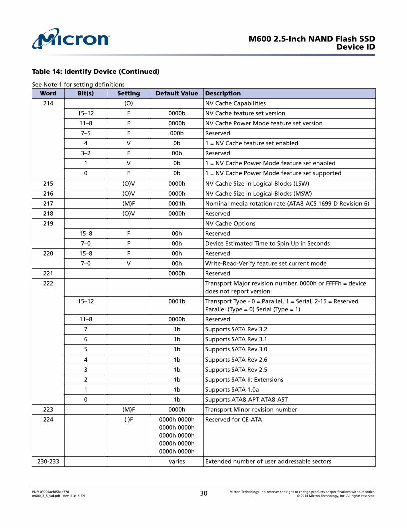
Table 14: Identify Device (Continued)
See Note 1 for setting definitionsWord Bit(s) Setting Default Value Description
214 (O) NV Cache Capabilities
15–12 F 0000b NV Cache feature set version
11–8 F 0000b NV Cache Power Mode feature set version
7–5 F 000b Reserved
4 V 0b 1 = NV Cache feature set enabled
3–2 F 00b Reserved
1 V 0b 1 = NV Cache Power Mode feature set enabled
0 F 0b 1 = NV Cache Power Mode feature set supported
215 (O)V 0000h NV Cache Size in Logical Blocks (LSW)
216 (O)V 0000h NV Cache Size in Logical Blocks (MSW)
217 (M)F 0001h Nominal media rotation rate (ATA8-ACS 1699-D Revision 6)
218 (O)V 0000h Reserved
219 NV Cache Options
15–8 F 00h Reserved
7–0 F 00h Device Estimated Time to Spin Up in Seconds
220 15–8 F 00h Reserved
7–0 V 00h Write-Read-Verify feature set current mode
221 0000h Reserved
222 Transport Major revision number. 0000h or FFFFh = devicedoes not report version
15–12 0001b Transport Type - 0 = Parallel, 1 = Serial, 2-15 = ReservedParallel (Type = 0) Serial (Type = 1)
11–8 0000b Reserved
7 1b Supports SATA Rev 3.2
6 1b Supports SATA Rev 3.1
5 1b Supports SATA Rev 3.0
4 1b Supports SATA Rev 2.6
3 1b Supports SATA Rev 2.5
2 1b Supports SATA II: Extensions
1 1b Supports SATA 1.0a
0 1b Supports ATA8-APT ATA8-AST
223 (M)F 0000h Transport Minor revision number
224 ( )F 0000h 0000h0000h 0000h0000h 0000h0000h 0000h0000h 0000h
Reserved for CE-ATA
230-233 varies Extended number of user addressable sectors
M600 2.5-Inch NAND Flash SSDDevice ID
PDF: 09005aef858ae778m600_2_5_ssd.pdf - Rev. E 3/15 EN 30 Micron Technology, Inc. reserves the right to change products or specifications without notice.
© 2014 Micron Technology, Inc. All rights reserved.
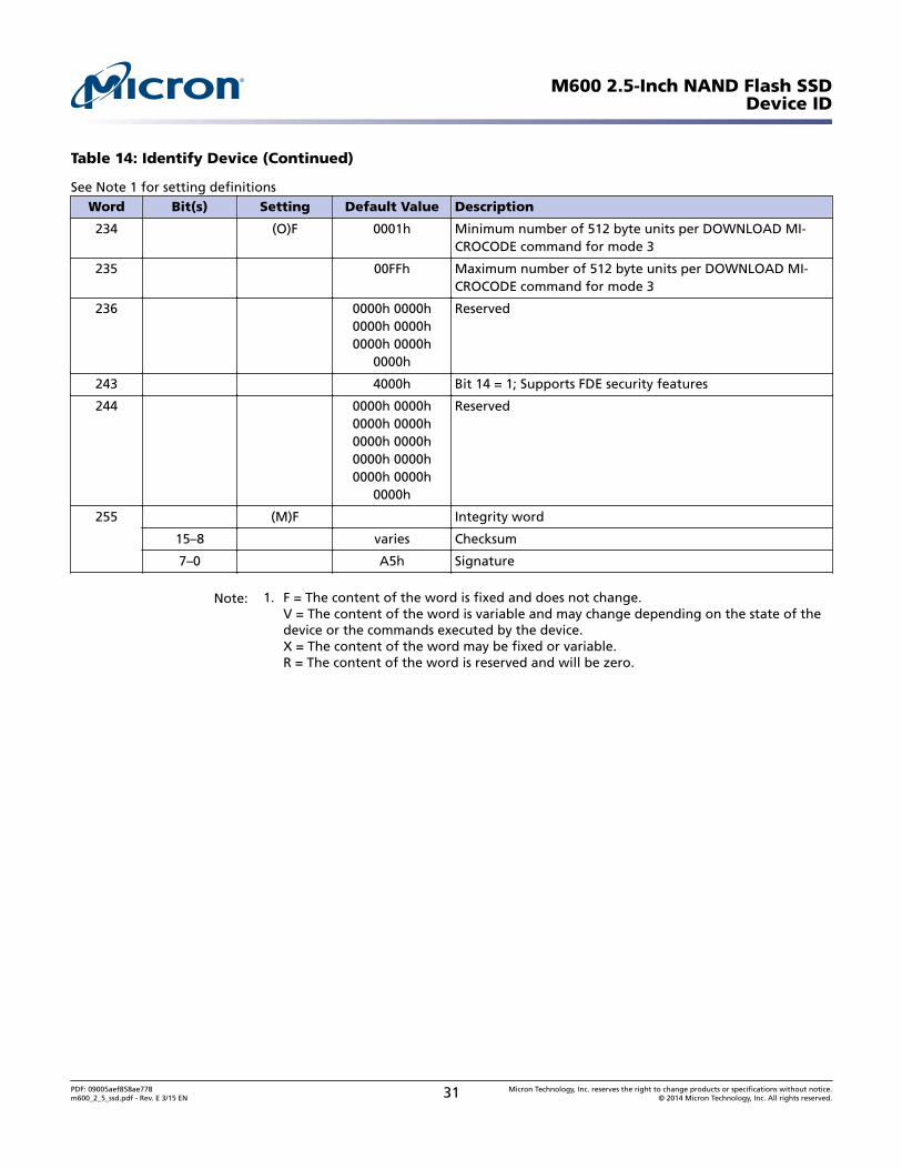
Table 14: Identify Device (Continued)
See Note 1 for setting definitionsWord Bit(s) Setting Default Value Description
234 (O)F 0001h Minimum number of 512 byte units per DOWNLOAD MI-CROCODE command for mode 3
235 00FFh Maximum number of 512 byte units per DOWNLOAD MI-CROCODE command for mode 3
236 0000h 0000h0000h 0000h0000h 0000h
0000h
Reserved
243 4000h Bit 14 = 1; Supports FDE security features
244 0000h 0000h0000h 0000h0000h 0000h0000h 0000h0000h 0000h
0000h
Reserved
255 (M)F Integrity word
15–8 varies Checksum
7–0 A5h Signature
Note: 1. F = The content of the word is fixed and does not change.V = The content of the word is variable and may change depending on the state of thedevice or the commands executed by the device.X = The content of the word may be fixed or variable.R = The content of the word is reserved and will be zero.
M600 2.5-Inch NAND Flash SSDDevice ID
PDF: 09005aef858ae778m600_2_5_ssd.pdf - Rev. E 3/15 EN 31 Micron Technology, Inc. reserves the right to change products or specifications without notice.
© 2014 Micron Technology, Inc. All rights reserved.
Commands
Table 15: Supported ATA Command Set
See ACS-3 standard for command detailsCommand Name Command Code (hex)
AMAC-GET NATIVE MAX ADDRESS EXT 78h/0000h
AMAC-SET ACCESSIBLE MAX ADDRESS EXT 78h/0001h
AMAC-FREEZE ACCESSIBLE MAX ADDRESS EXT 78h/0002h
CHECK POWER MODE 98h or E5h
DATA SET MANAGEMENT – TRIM 06h/0001h
DOWNLOAD MICROCODE 92h
EXECUTE DEVICE DIAGNOSTIC 90h
FLUSH CACHE E7h
FLUSH CACHE EXT EAh
IDENTIFY DEVICE ECh
IDLE E3h or 97h
IDLE IMMEDIATE E1h or 95h
INITIALIZE DEVICE PARAMETERS 91h
READ BUFFER E4h
READ DMA (with retry) C8h
READ DMA (without retry) C9h
READ DMA EXT 25h
READ FPDMA QUEUED 60h
READ LOG EXT 2Fh
READ MULTIPLE C4h
READ MULTIPLE EXT 29h
READ SECTOR(S) EXT 24h
READ SECTOR(S) (with retry) 20h
READ SECTOR(S) (without retry) 21h
READ VERIFY SECTOR EXT 42h
READ VERIFY SECTOR(S) (with retry) 40h
RECEIVE FPDMA QUEUED 65h
SANITIZE DEVICE B4h
SCT WRITE SAME 02h/0001h02h/0002h02h/0101h02h/0102h
SCT SET ERROR RECOVERY CONTROL 03h/01h
SCT SET FEATURE CONTROL 04h/01h
SCT RETURN FEATURE CONTROL 04h/02h
SCT RETURN FEATURE OPTION FLAG 04h/03h
SCT RETURN SCT DATA TABLE 05h/01h
M600 2.5-Inch NAND Flash SSDCommands
PDF: 09005aef858ae778m600_2_5_ssd.pdf - Rev. E 3/15 EN 32 Micron Technology, Inc. reserves the right to change products or specifications without notice.
© 2014 Micron Technology, Inc. All rights reserved.

Table 15: Supported ATA Command Set (Continued)
See ACS-3 standard for command detailsCommand Name Command Code (hex)
SECURITY DISABLE PASSWORD F6h
SECURITY ERASE PREPARE F3h
SECURITY ERASE UNIT F4h
SECURITY FREEZE LOCK F5h
SECURITY SET PASSWORD F1h
SECURITY UNLOCK F2h
SEND FPDMA QUEUED 64h
SET FEATURES EFh
SET MULTIPLE MODE C6h
SLEEP E6h or 99h
SMART DISABLE OPERATIONS B0h/D9h
SMART ENABLE OPERATIONS B0h/D8h
SMART ENABLE/DISABLE AUTOSAVE B0h/D2h
SMART EXECUTE OFF-LINE IMMEDIATE B0h/D4h
SMART READ DATA B0h/D0h
SMART READ LOG SECTOR B0h/D5h
SMART RETURN STATUS B0h/DAh
SMART WRITE LOG B0h/D6h
STANDBY E2h or 96h
STANDBY IMMEDIATE E0h or 94h
TRUSTED NON-DATA 5Bh
TRUSTED RECEIVE 5Ch
TRUSTED RECEIVE DMA 5Dh
TRUSTED SEND 5Eh
TRUSTED SEND DMA 5Fh
WRITE BUFFER E8h
WRITE DMA (with retry) CAh
WRITE DMA (without retry) CBh
WRITE DMA EXT 35h
WRITE DMA FUA EXT 3Dh
WRITE FPDMA QUEUED 61h
WRITE LOG EXT 3Fh
WRITE MULTIPLE C5h
WRITE MULTIPLE EXT 39h
WRITE MULTIPLE FUA EXT CEh
WRITE SECTOR(S) (with retry) 30h
WRITE SECTOR(S) EXT 34h
M600 2.5-Inch NAND Flash SSDCommands
PDF: 09005aef858ae778m600_2_5_ssd.pdf - Rev. E 3/15 EN 33 Micron Technology, Inc. reserves the right to change products or specifications without notice.
© 2014 Micron Technology, Inc. All rights reserved.
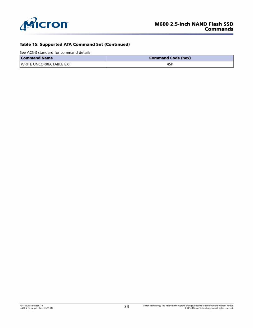
Table 15: Supported ATA Command Set (Continued)
See ACS-3 standard for command detailsCommand Name Command Code (hex)
WRITE UNCORRECTABLE EXT 45h
M600 2.5-Inch NAND Flash SSDCommands
PDF: 09005aef858ae778m600_2_5_ssd.pdf - Rev. E 3/15 EN 34 Micron Technology, Inc. reserves the right to change products or specifications without notice.
© 2014 Micron Technology, Inc. All rights reserved.
ComplianceMicron SSDs comply with the following:
• RoHS “green”• CE (Europe): EN55022, 2006 Class B and EN55024, 1998 + A1: 2001 + A2:2003• FCC: CFR Title 47, Part 15, ICES-003, all Class B• UL (US): approval to UL-60950-1, 2nd Edition, 2007-03-27, IEC 60950-1:2005, 2nd Ed-
ition• BSMI (Taiwan): approval to CNS 13438• C-TICK (Australia, New Zealand): approval to AS/NZS CISPR22• KCC RRL (Korea): approval to KN22 Class B, KN 24 Class B• W.E.E.E.: Compliance with EU WEEE directive 2002/96/EC. Additional obligations
may apply to customers who place these products in the markets where WEEE is en-forced.
• TUV (Germany): approval to IEC60950/EN60950• VCCI
• IC (Canada):- This Class B digital apparatus complies with Canadian ICES-003.- Cet appareil numérique de la classe B est conforme à la norme NMB-003 du Canada.
FCC Rules
This equipment has been tested and found to comply with the limits for a Class B digitaldevice, pursuant to part 15 of the FCC Rules. These limits are designed to provide rea-sonable protection against harmful interference in a residential installation. This equip-ment generates, uses, and can radiate radio frequency energy and, if not installed andused in accordance with the instructions, may cause harmful interference to radio com-munications. However, there is no guarantee that interference will not occur in a partic-ular installation. If this equipment does cause harmful interference to radio or televi-sion reception, which can be determined by turning the equipment off and on, the useris encouraged to try to correct the interference by one or more of the following meas-ures:
• Reorient or relocate the receiving antenna.• Increase the separation between the equipment and the receiver.• Connect the equipment into an outlet on a circuit different from that to which the re-
ceiver is connected.• Consult the dealer or an experienced radio/TV technician for help.
M600 2.5-Inch NAND Flash SSDCompliance
PDF: 09005aef858ae778m600_2_5_ssd.pdf - Rev. E 3/15 EN 35 Micron Technology, Inc. reserves the right to change products or specifications without notice.
© 2014 Micron Technology, Inc. All rights reserved.
References• Serial ATA: High-speed serialized AT attachment, Serial ATA working group, available
at www.sata-io.org• SATA 3.2 GOLD• ATA-8 ACS3 (T13/2161-D, Revision 4k)• TCG Storage Security Subsystem Class Opal; Specification 2.00 Revision 1.00, Feb 24,
2012• TCG Core Specification; Specification 2.00 Revision 2.00, Nov 4, 2011• TCG Storage Interface Interactions: Specification Version 1.02 Revision 1.00 30 De-
cember, 2011• IEEE-1667: "Standard Protocol for Authentication in Host Attachments of Transient
Storage Devices"• SFF 8201 Rev 2.7: For form factor
M600 2.5-Inch NAND Flash SSDReferences
PDF: 09005aef858ae778m600_2_5_ssd.pdf - Rev. E 3/15 EN 36 Micron Technology, Inc. reserves the right to change products or specifications without notice.
© 2014 Micron Technology, Inc. All rights reserved.
Revision History
Rev. E – 3/15
• Updated table 13: TCG/Opal Support Parameters in TCG/Opal Support• Updated table 14: Identify Device in Device ID• Updated table 15: Supported ATA Command Set in Commands
Rev. D – 12/14
• Updated Feature (Deleted Mechanical, Added 2.5 inch x 7mm form factor)• Updated Physical Configuration (Added modified package dimensions)• Deleted Package Dimensions (Moved to Physical Configuration)• Deleted Compliance• Updated References
Rev. C – 9/14
• Updated Endurance: Total bytes written in Feature up to 144 to 400TB.• Updated Part Number Chart.• Updated table 8: Drive Lifetime and notes in Endurance.• Added Dynamic Write Acceleration.• Updated Adaptive Thermal Monitoring.• Updated Package Dimensions
Rev. B – 7/14
• Updated part numbers.• Updated Operating temperature note on page 1.• Updated Part Number Chart.• Updated values in the Drive Performance table.• Updated notes in the Drive Lifetime – Client Computing table.• Updated values and notes in the SATA Power Consumption table.• Updated notes in the Maximum Ratings table.• Deleted 5mm-high mechanical drawing and information through out.
Rev. A – 3/14
• Initial release.
8000 S. Federal Way, P.O. Box 6, Boise, ID 83707-0006, Tel: 208-368-4000www.micron.com/products/support Sales inquiries: 800-932-4992
Micron and the Micron logo are trademarks of Micron Technology, Inc.All other trademarks are the property of their respective owners.
This data sheet contains minimum and maximum limits specified over the power supply and temperature range set forth herein.Although considered final, these specifications are subject to change, as further product development and data characterization some-
times occur.
M600 2.5-Inch NAND Flash SSDRevision History
PDF: 09005aef858ae778m600_2_5_ssd.pdf - Rev. E 3/15 EN 37 Micron Technology, Inc. reserves the right to change products or specifications without notice.
© 2014 Micron Technology, Inc. All rights reserved.