Embed Size (px)
Citation preview
The Aberration Corrected SEM
David C JoyUniversity of Tennessee and
Oak Ridge National Laboratory
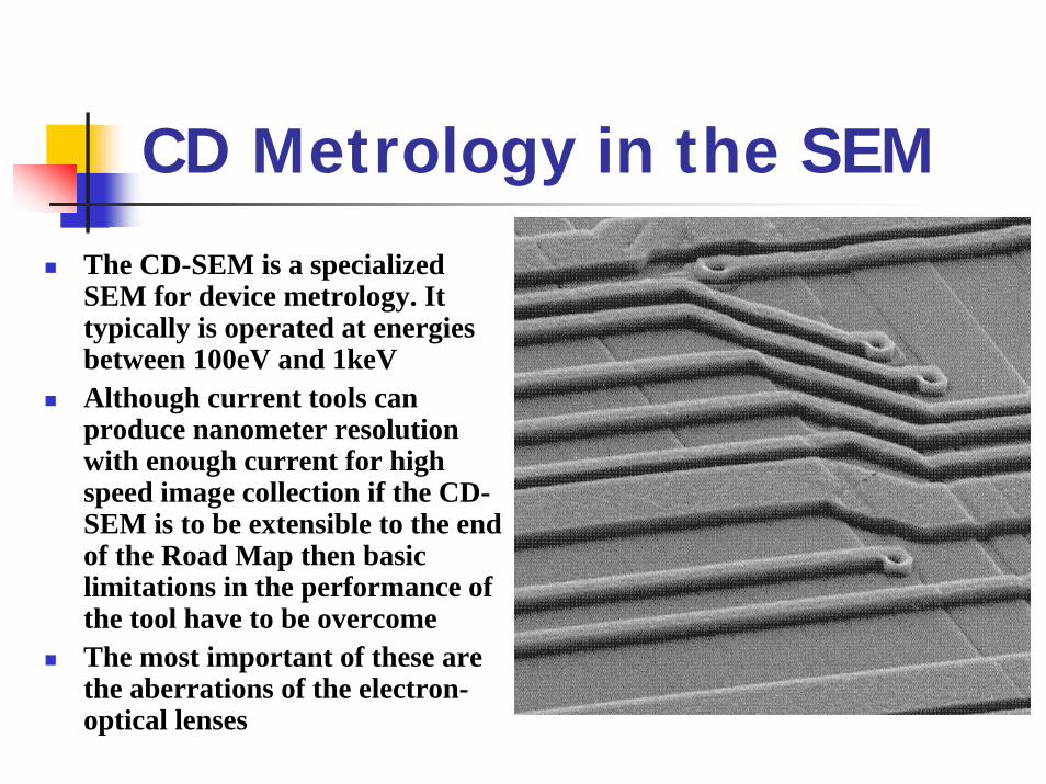
CD Metrology in the SEMThe CD-SEM is a specialized SEM for device metrology. It typically is operated at energies between 100eV and 1keV Although current tools can produce nanometer resolution with enough current for high speed image collection if the CD-SEM is to be extensible to the end of the Road Map then basic limitations in the performance of the tool have to be overcomeThe most important of these are the aberrations of the electron-optical lenses
Aberrations in the CD-SEM
The three key aberrations for the CD-SEM in order of significance are;Chromatic aberrationDiffractionSpherical aberrationAs shown by Scherzer (1936) each is inevitable and optimizing the balance between them leads to undesirable restrictions on performanceAberration coefficients scale with focal length and lens size so high performance lenses are restrictive
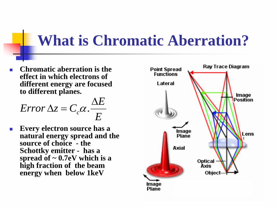
What is Chromatic Aberration?
Chromatic aberration is the effect in which electrons of different energy are focused to different planes.
Every electron source has a natural energy spread and the source of choice - the Schottky emitter - has a spread of ~ 0.7eV which is a high fraction of the beam energy when below 1keV
EECzError c
∆=∆ .α
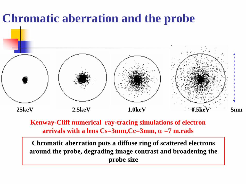
Chromatic aberration and the probe
25keV 5nm2.5keV 1.0keV 0.5keV
Kenway-Cliff numerical ray-tracing simulations of electron arrivals with a lens Cs=3mm,Cc=3mm, α =7 m.rads
Chromatic aberration puts a diffuse ring of scattered electrons around the probe, degrading image contrast and broadening the
probe size
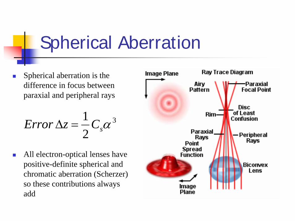
Spherical Aberration
Spherical aberration is the difference in focus between paraxial and peripheral rays
All electron-optical lenses have positive-definite spherical and chromatic aberration (Scherzer) so these contributions always add
3
21 αsCzError =∆
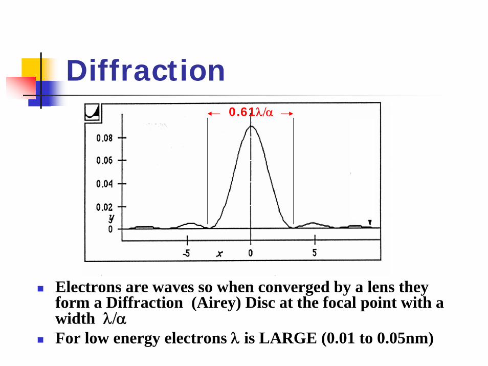
Diffraction0.61λ/α
Electrons are waves so when converged by a lens they form a Diffraction (Airey) Disc at the focal point with a width λ/αFor low energy electrons λ is LARGE (0.01 to 0.05nm)
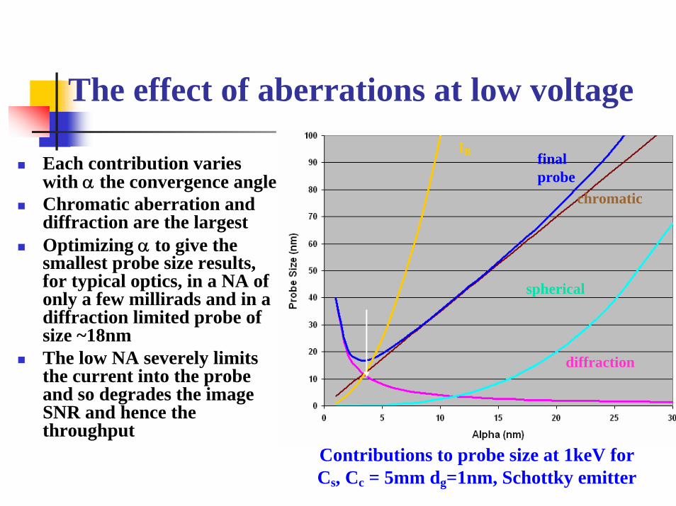
The effect of aberrations at low voltage
Each contribution varies with α the convergence angleChromatic aberration and diffraction are the largest Optimizing α to give the smallest probe size results, for typical optics, in a NA of only a few millirads and in a diffraction limited probe of size ~18nmThe low NA severely limits the current into the probe and so degrades the image SNR and hence the throughput
Contributions to probe size at 1keV for Cs, Cc = 5mm dg=1nm, Schottky emitter
IB final probe
chromatic
spherical
diffraction
Overcoming aberrationsScherzer showed in 1936 that all normal electron-optical lenses had ‘positive definite’ aberrationsBut later (1947) Scherzer showed that lenses which were not cylindrically symmetrical such as multi-poles, or in which the electron energy changed with time, could have either positive or negative aberration coefficientsSince then many groups have worked to exploit this loophole and produce a compound electron optical lens with reduced aberrationcoefficientsHillier and Ramberg’s “Stigmator” (1947) was the first example -using a multi-pole (weak quadrupole) device used to correct the geometrical aberration that produces astigmatism
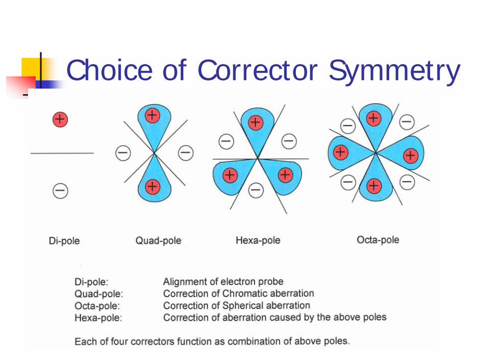
Choice of Corrector Symmetry
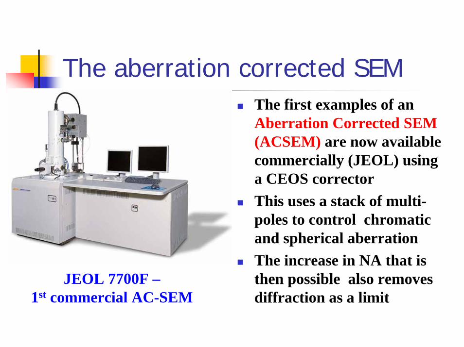
The aberration corrected SEMThe first examples of an Aberration Corrected SEM (ACSEM) are now available commercially (JEOL) using a CEOS correctorThis uses a stack of multi-poles to control chromatic and spherical aberrationThe increase in NA that is then possible also removes diffraction as a limit
JEOL 7700F –1st commercial AC-SEM
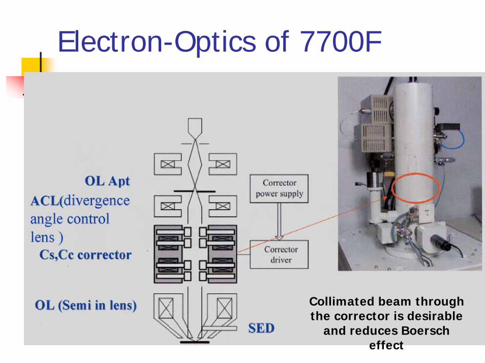
Electron-Optics of 7700F
Collimated beam through the corrector is desirable
and reduces Boerscheffect
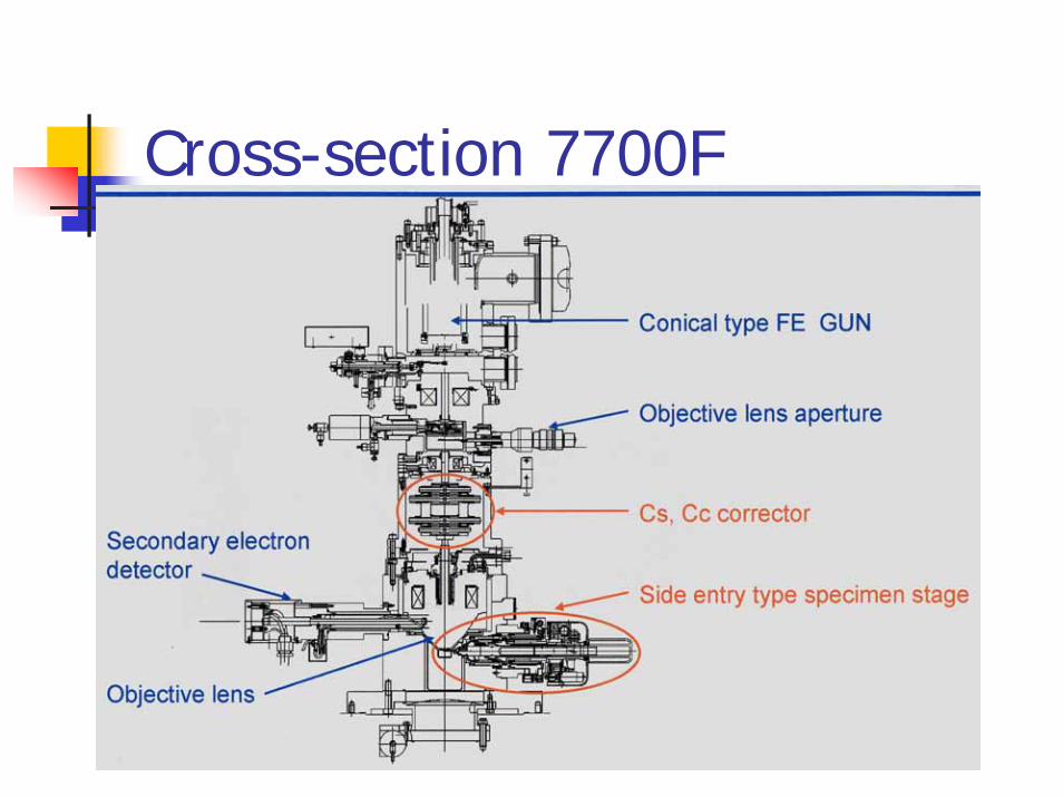
Cross-section 7700F
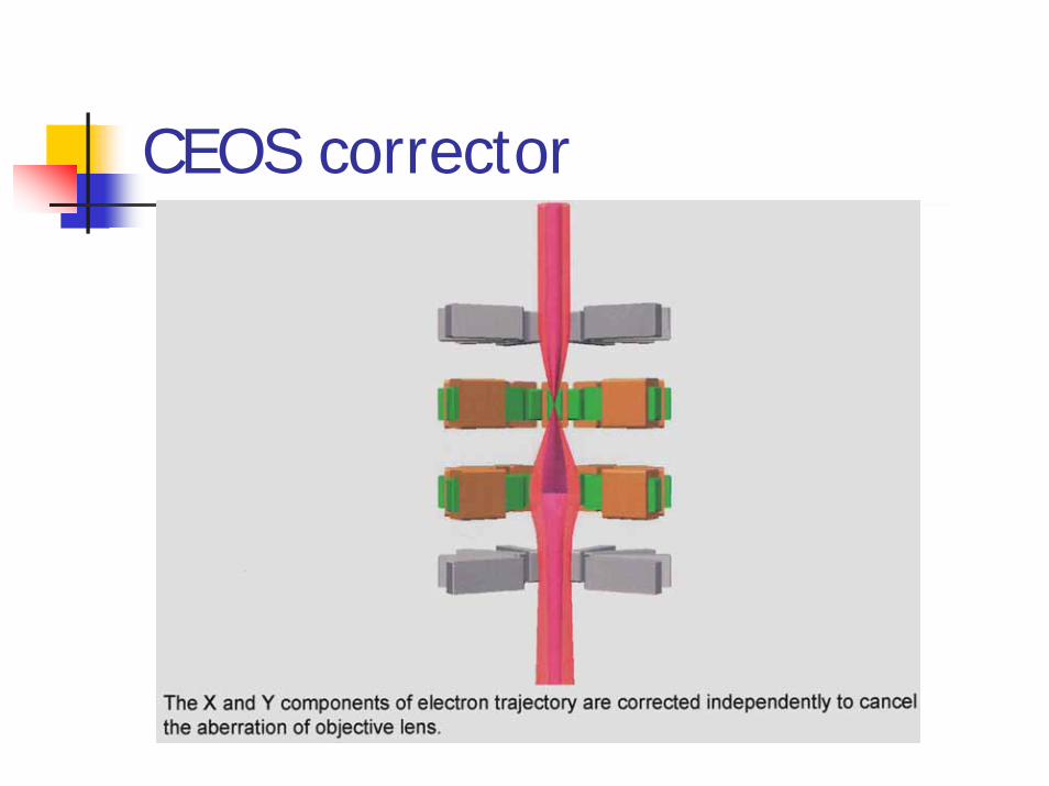
CEOS corrector
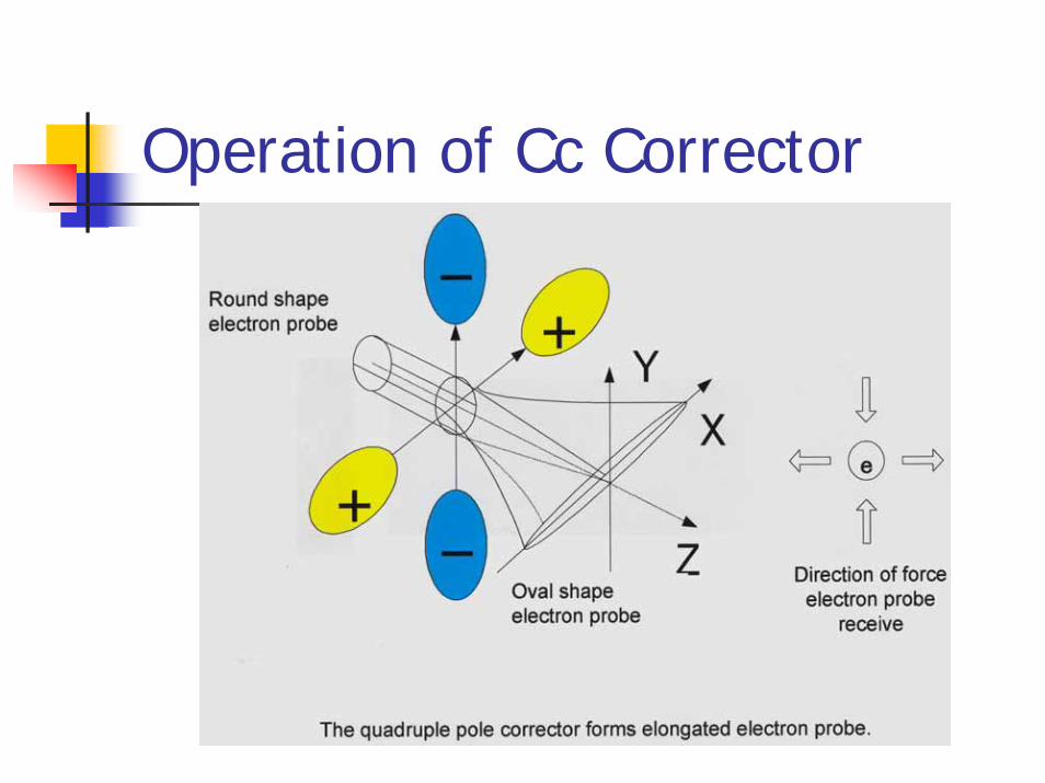
Operation of Cc Corrector
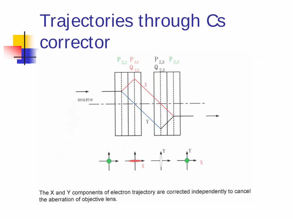
Trajectories through Cs corrector
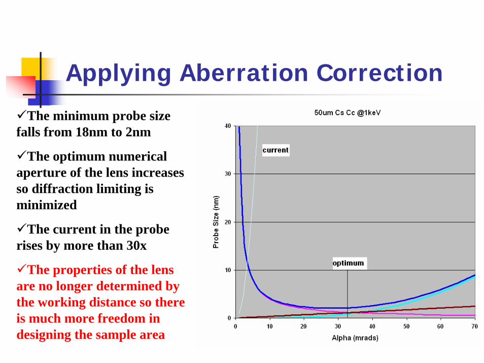
Applying Aberration Correction
The minimum probe size falls from 18nm to 2nm
The optimum numerical aperture of the lens increases so diffraction limiting is minimized
The current in the probe rises by more than 30x
The properties of the lens are no longer determined by the working distance so there is much more freedom in designing the sample area
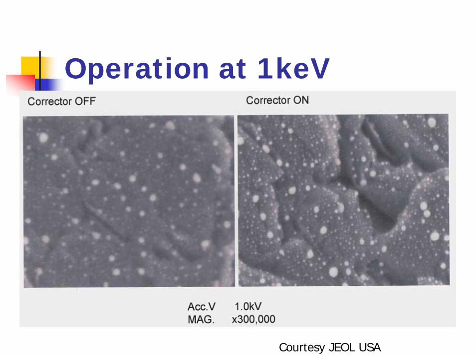
Operation at 1keV
Courtesy JEOL USA
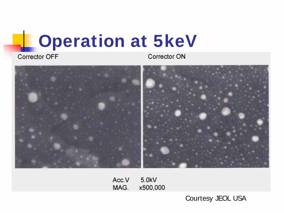
Operation at 5keV
Courtesy JEOL USA
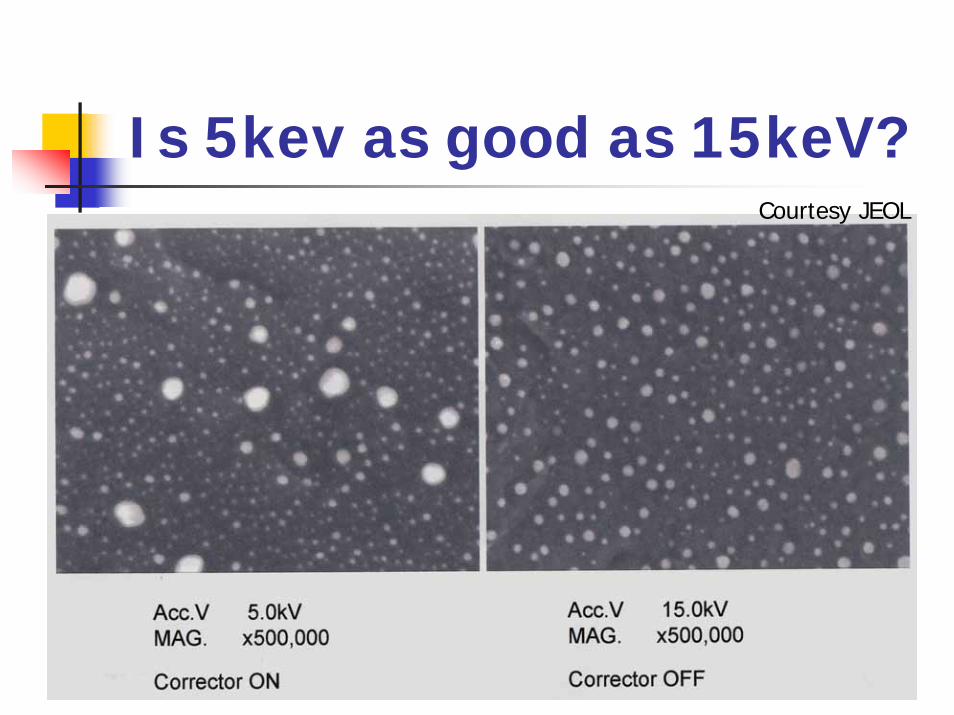
Is 5kev as good as 15keV?Courtesy JEOL
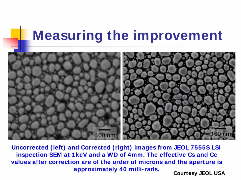
Measuring the improvement
Uncorrected (left) and Corrected (right) images from JEOL 7555S LSI inspection SEM at 1keV and a WD of 4mm. The effective Cs and Cc
values after correction are of the order of microns and the aperture is approximately 40 milli-rads.
Courtesy JEOL USA
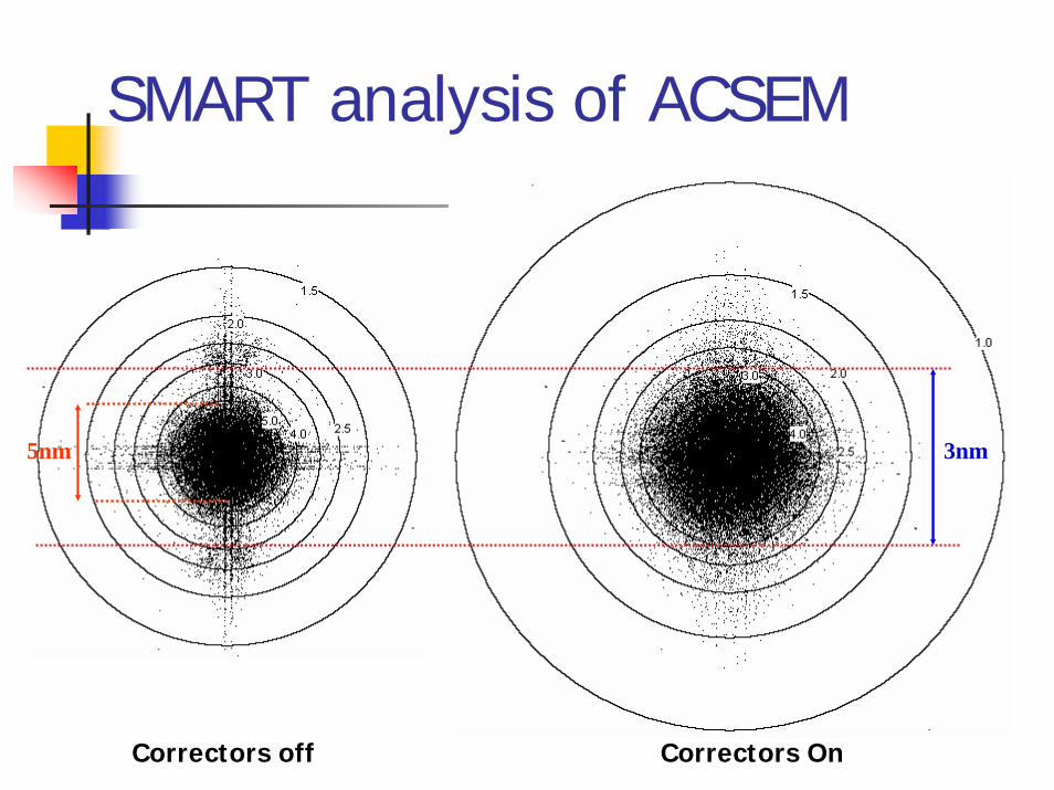
SMART analysis of ACSEM
3nm5nm
Correctors off Correctors On
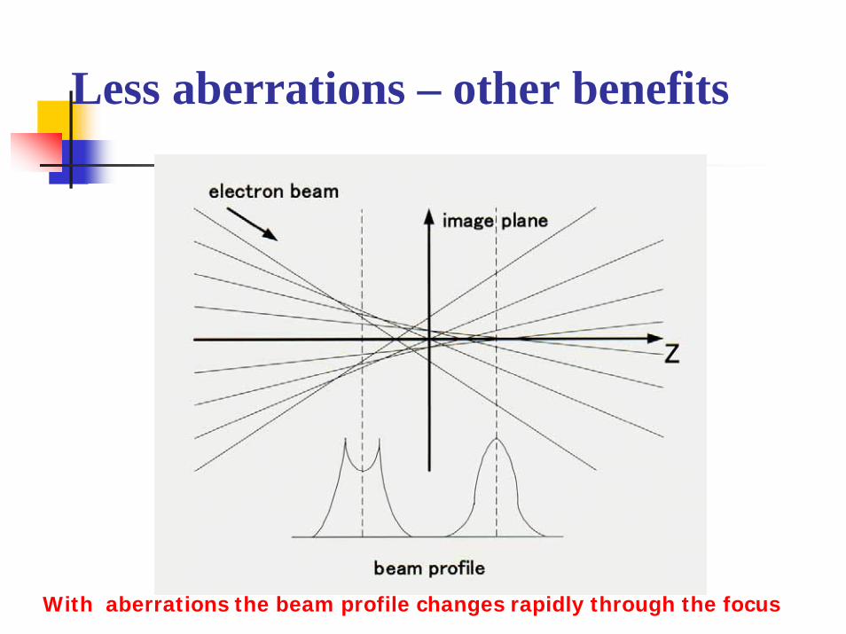
Less aberrations – other benefits
With aberrations the beam profile changes rapidly through the focus
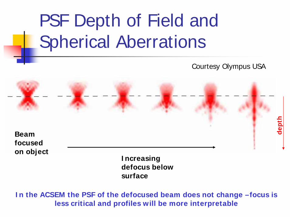
PSF Depth of Field and Spherical Aberrations
Courtesy Olympus USA
Beam focused on object
Increasing defocus below surface
dept
h
In the ACSEM the PSF of the defocused beam does not change –focus is less critical and profiles will be more interpretable
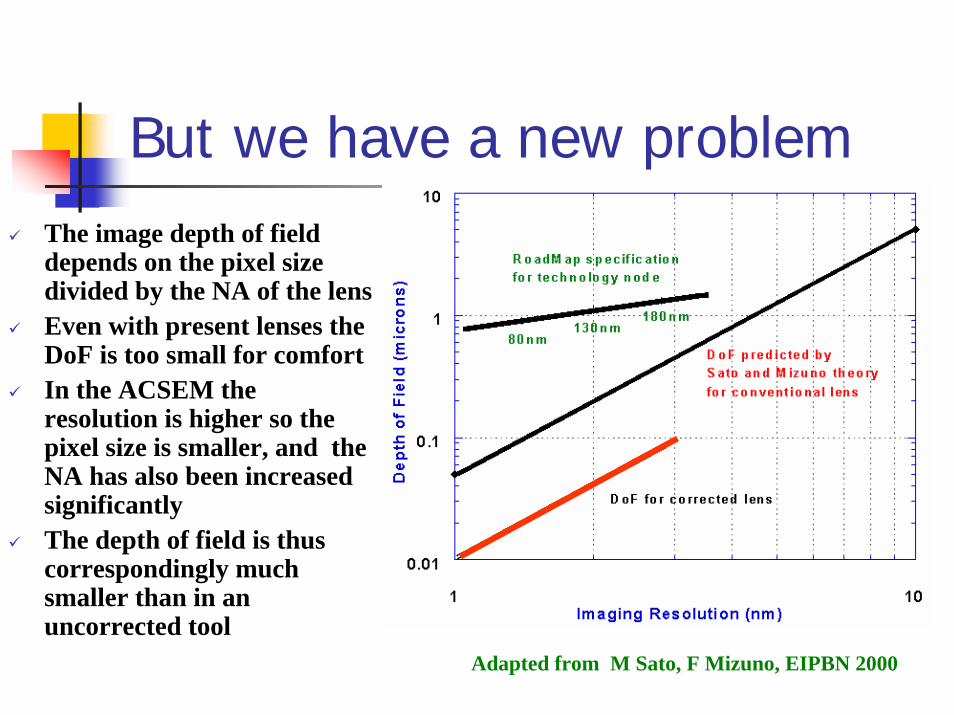
But we have a new problemThe image depth of field depends on the pixel size divided by the NA of the lensEven with present lenses the DoF is too small for comfortIn the ACSEM the resolution is higher so the pixel size is smaller, and the NA has also been increased significantlyThe depth of field is thus correspondingly much smaller than in an uncorrected tool
Adapted from M Sato, F Mizuno, EIPBN 2000
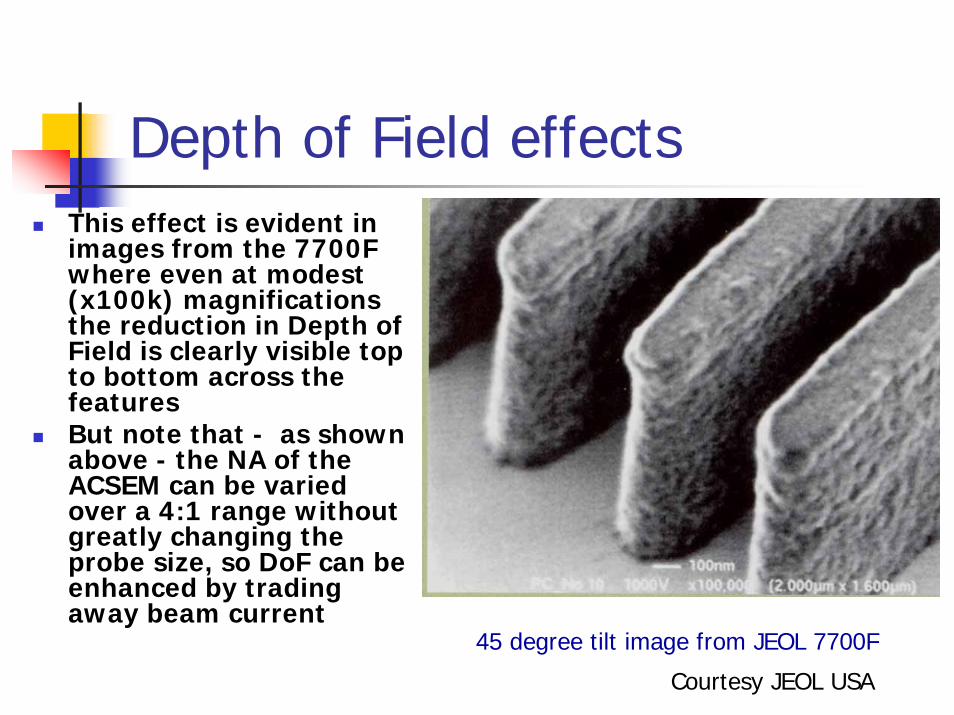
Depth of Field effectsThis effect is evident in images from the 7700F where even at modest (x100k) magnifications the reduction in Depth of Field is clearly visible top to bottom across the featuresBut note that - as shown above - the NA of the ACSEM can be varied over a 4:1 range without greatly changing the probe size, so DoF can be enhanced by trading away beam current
45 degree tilt image from JEOL 7700F
Courtesy JEOL USA
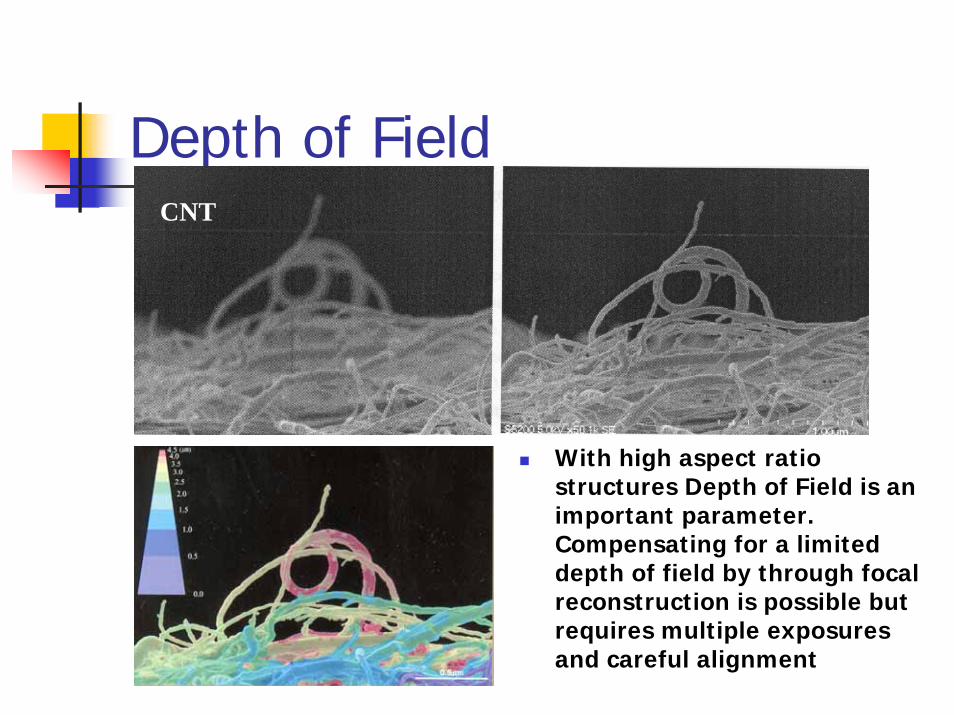
Depth of Field
With high aspect ratio structures Depth of Field is an important parameter. Compensating for a limited depth of field by through focal reconstruction is possible but requires multiple exposures and careful alignment
CNT
What happens next ?
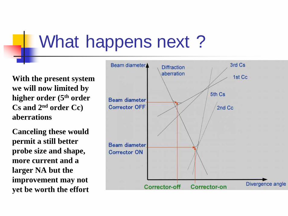
With the present system we will now limited by higher order (5th order Cs and 2nd order Cc) aberrations
Canceling these would permit a still better probe size and shape, more current and a larger NA but the improvement may not yet be worth the effort
Final points on the AC CD-SEM
Aberration correction is expensive adding $500k per column to the base costAberration correctors require exact set-up and may require frequent adjustments. Although automated these operations are non-trivial and the algorithms required to perform it on the ACSEM are not as rugged as those for TEM and STEM and suitable targets are absentAberration correction does not only benefit high resolution instruments . . . .
Other candidate for ACAnalytical SEMs – aberration correction would give a major increase in beam current (without an increase in probe size) for improved chemical sensitivity, and allow better access below the lens for X-ray detectorsDefect detection tools would benefit from higher reading speeds and lower error ratesElectron beam lithography tools would have higher writing speeds and smaller probes without the need to upgrade electron sources
Acknowledgements
To Charlie Nielsen (JEOL USA) for his help in providing the experimental data and for permission to show the results originally published in JEOL NewsTo Prof. Harald Rose for developing the practical aberration corrector, and to Larry Allard, Steve Pennycook, Edgar Volkl (ORNL) for valuable discussions and insights on aberration correction
The importance of OTF
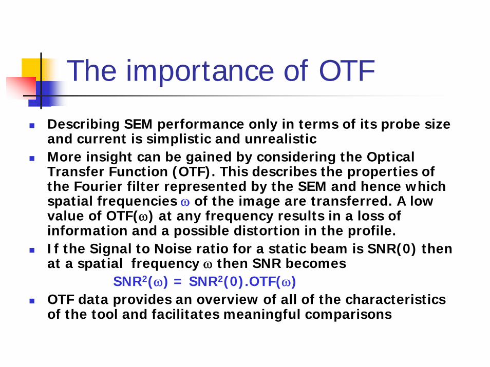
Describing SEM performance only in terms of its probe size and current is simplistic and unrealisticMore insight can be gained by considering the Optical Transfer Function (OTF). This describes the properties of the Fourier filter represented by the SEM and hence which spatial frequencies ω of the image are transferred. A low value of OTF(ω) at any frequency results in a loss of information and a possible distortion in the profile. If the Signal to Noise ratio for a static beam is SNR(0) then at a spatial frequency ω then SNR becomes
SNR2(ω) = SNR2(0).OTF(ω)OTF data provides an overview of all of the characteristics of the tool and facilitates meaningful comparisons
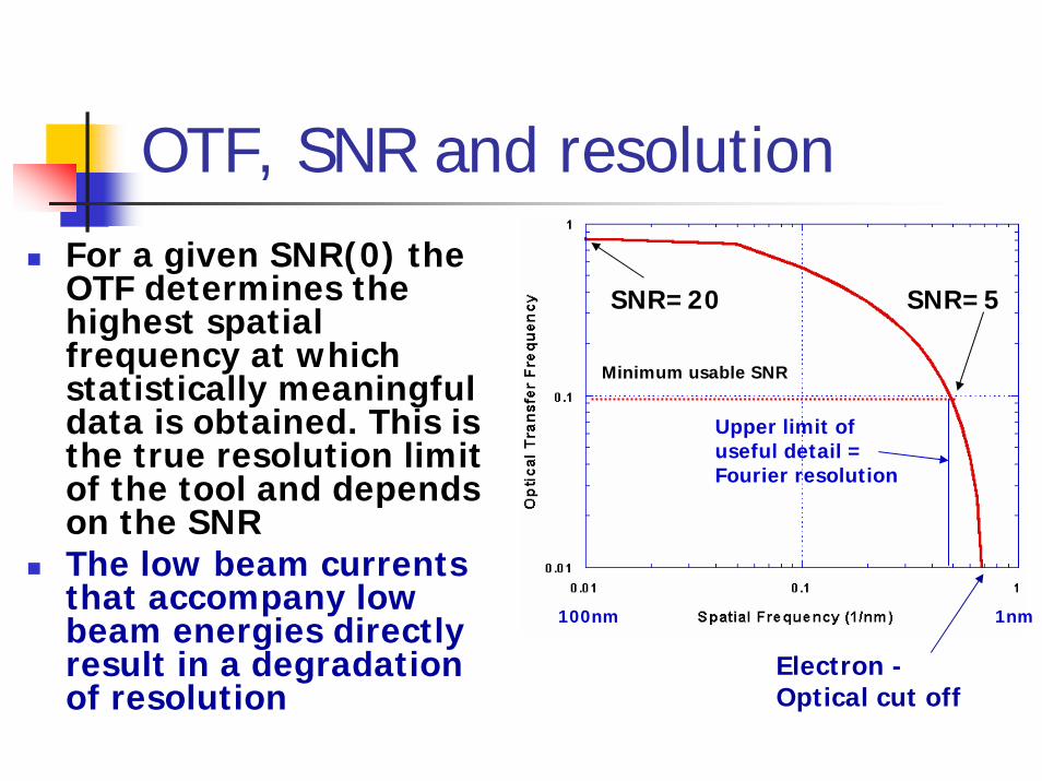
OTF, SNR and resolution
Electron -Optical cut off
100nm 1nm
SNR=20 SNR=5
Minimum usable SNR
Upper limit of useful detail = Fourier resolution
For a given SNR(0) the OTF determines the highest spatial frequency at which statistically meaningful data is obtained. This is the true resolution limit of the tool and depends on the SNRThe low beam currents that accompany low beam energies directly result in a degradation of resolution
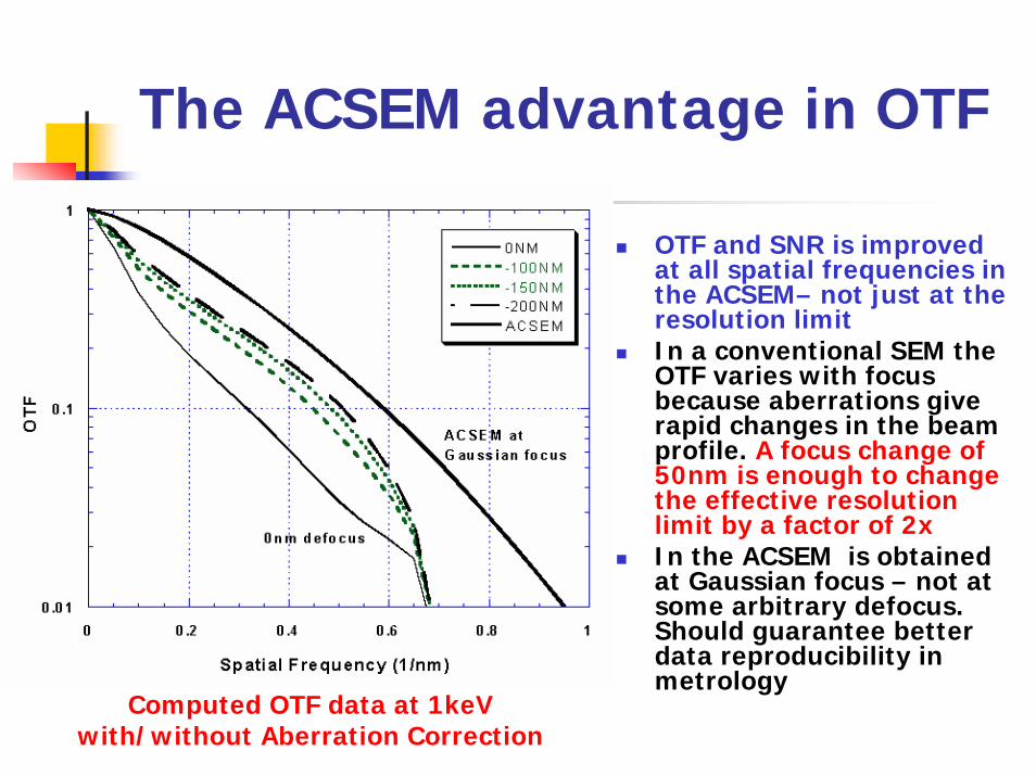
The ACSEM advantage in OTF
OTF and SNR is improved at all spatial frequencies in the ACSEM– not just at the resolution limitIn a conventional SEM the OTF varies with focus because aberrations give rapid changes in the beam profile. A focus change of 50nm is enough to change the effective resolution limit by a factor of 2xIn the ACSEM is obtained at Gaussian focus – not at some arbitrary defocus. Should guarantee better data reproducibility in metrology
Computed OTF data at 1keV with/without Aberration Correction
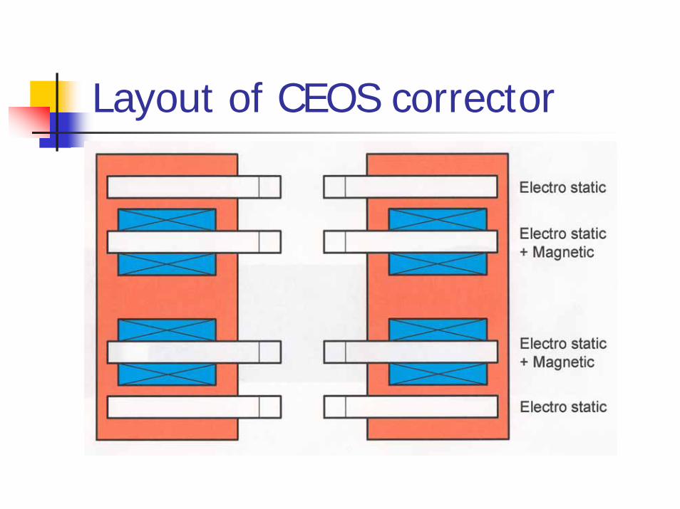
Layout of CEOS corrector
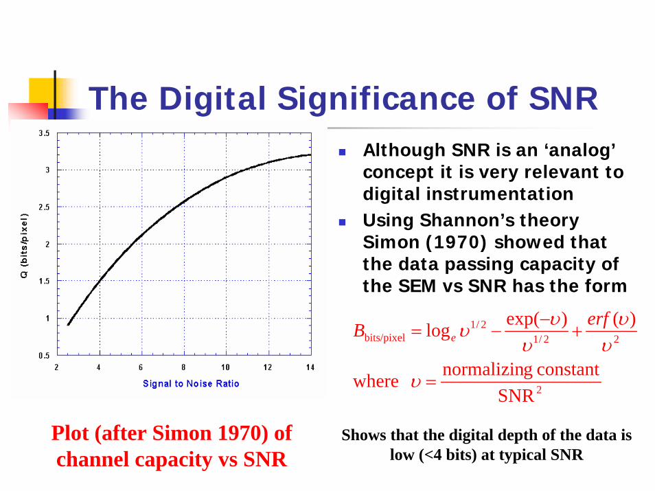
The Digital Significance of SNRAlthough SNR is an ‘analog’concept it is very relevant to digital instrumentationUsing Shannon’s theory Simon (1970) showed that the data passing capacity of the SEM vs SNR has the form
Plot (after Simon 1970) of channel capacity vs SNR
2
22/12/1
bits/pixel
SNRconstant gnormalizin where
)()exp(log
=
+−
−=
υ
υυ
υυυ erfB e
Shows that the digital depth of the data is low (<4 bits) at typical SNR