Embed Size (px)
Citation preview

HAL Id: hal-00587048https://hal.archives-ouvertes.fr/hal-00587048
Submitted on 19 Apr 2011
HAL is a multi-disciplinary open accessarchive for the deposit and dissemination of sci-entific research documents, whether they are pub-lished or not. The documents may come fromteaching and research institutions in France orabroad, or from public or private research centers.
L’archive ouverte pluridisciplinaire HAL, estdestinée au dépôt et à la diffusion de documentsscientifiques de niveau recherche, publiés ou non,émanant des établissements d’enseignement et derecherche français ou étrangers, des laboratoirespublics ou privés.
Microstructural changes induced by low energy heavyion irradiation in titanium silicon carbide
Jean-Christophe Nappé, Claire Maurice, Philippe Grosseau, F. Audubert, L.Thomé, Bernard Guilhot, Michel Beauvy, Mourad Benabdesselam
To cite this version:Jean-Christophe Nappé, Claire Maurice, Philippe Grosseau, F. Audubert, L. Thomé, et al..Microstructural changes induced by low energy heavy ion irradiation in titanium silicon car-bide. Journal of the European Ceramic Society, Elsevier, 2011, 31 (8), pp.1503-1511.�10.1016/j.jeurceramsoc.2011.01.002�. �hal-00587048�
Microstructural changes induced by low energy heavy ion irradiation in titanium silicon carbide
Authors
J.C. Nappéa,† C. Mauriceb, Ph. Grosseaua, F. Audubertc, L. Thoméd, B. Guilhote, M. Beauvyc, M. Benabdesselamf
a École Nationale Supérieure des Mines, SPIN/PMMC, LPMG UMR CNRS 5148, 158 cours Fauriel, 42023 Saint-Étienne cedex 2, France b École Nationale Supérieure des Mines, SMS/MPM, PECM UMR CNRS 5146, 158 cours Fauriel, 42023 Saint-Étienne cedex 2, France c CEA, DEN, DEC/SPUA/LTEC, Cadarache, 13108 St Paul lez Durance, France d Centre de Spectrométrie Nucléaire et de Spectrométrie de Masse, CNRS-IN2P3-Université Paris Sud, Bât. 108, 91405 Orsay, France e École Nationale Supérieure des Mines, CIS/B2M, 158 cours Fauriel, 42023 Saint-Étienne cedex 2, France f Université de Nice - Sophia Antipolis, LPMC UMR CNRS 6622, Parc Valrose, 06108 Nice cedex 2, France
ABSTRACT
Low energy ion irradiation was used to investigate the microstructural modifications induced in Ti3SiC2 by nuclear collisions. Characterization of the microstructure of the pristine sample by electron back-scatter diffraction (EBSD) shows a strong texturing of TiSi2, which is a common secondary phase present in Ti3SiC2. A methodology based on atomic force microscopy (AFM) was developed to measure the volume swelling induced by ion irradiation, and it was validated on irradiated silicon carbide. The swelling of Ti3SiC2 was estimated to 2.2 ±0.8 % for an irradiation dose of 4.3 dpa at room temperature. Results obtained by both EBSD and AFM analyzes showed that nuclear collisions induce an anisotropic swelling in Ti3SiC2.
Keywords: Ti3SiC2, nuclear interaction, electron back-scatter diffraction, atomic force microscopy, anisotropic swelling
PACS: 81.05.Je, 61.80.Lj, 25.75.Ag, 28.41.Bm, 68.37.Ps, 61.05.J-
1. Introduction
The Gas-cooled Fast Reactor (GFR) is one of six new systems studied in the framework of the Generation IV International Forum (GIF). These systems are characterized by an increased security level, a better economic competitiveness, and the ability to recycle all the fuel in order to upgrade it to a fissionable material and to minimize long-lived waste production by transmutation [1]. The GFR is designed to work under helium-pressure and at high-temperature (1100-1300 K). Due to these working conditions, non-oxide refractory ceramics are required as fuel cladding. Thus, carbides turn out to be excellent candidates due to their remarkable mechanical and thermal properties. However, their behavior under irradiation has to be investigated.
Among potential carbides, ternary Ti3SiC2 presents some interesting properties. In 1972 Nickl et al. [2] remarked that this material is abnormally soft for a carbide, so that its hardness decreases as the applied load increases. For this reason Goto et al. [3] qualified Ti3SiC2 as a “ductile ceramic”. Furthermore, Ti3SiC2 combines the properties of metals with those usually attributed to ceramics [4-7]. Thus, this material is not only soft but also stiff and tough, it behaves as a good electrical and thermal conductor, and it can be easily machined with the tools generally used for steels.
† Corresponding author. Tel.: +33 477 420 213; fax: +33 477 499 694. E-mail address: [email protected] (JC. Nappé).
1

The interesting mechanical properties of Ti3SiC2 suggest that this compound could be used as fuel cladding material. Its damage tolerance to mechanical stresses might indicate a high resistance to irradiation. Nevertheless, apart from few recently published articles related to Ti3SiC2 [8-10], and Ti3(Si,Al)C2 [11-14], few information is available about its behavior under irradiation.
Previously [15,16], we showed that an irradiation performed at room temperature with 4 MeV Au ions to a fluence of 1019 m-2 induces both an erosion of the Ti3SiC2 grain boundaries, as observed by scanning electron microscopy, and a revealing of the grain structure, as evidenced by atomic force microscopy. We attributed the former phenomenon to a preferential sputtering due to lower threshold displacement energy of the atoms located in grain boundaries. For the latter result, we were led to consider the occurrence of preferential sputtering as a function of the crystallite orientation. In this work, complementary irradiation experiments suggest another explanation.
2. Experimental
The polycrystalline samples were provided by the 3-ONE-2 company (Vorhees, NJ, USA). They consist of about 74 % Ti3SiC2, 19 % TiC0.92, and 7 % TiSi2 (as estimated by X-ray diffraction). As-received samples were polished with diamond paste of a size down to 1 micron.
The interactions occurring in reactors are essentially elastic (or nuclear) collisions due to primary knock-on atoms from neutrons, and recoil atoms arising from alpha-decays. In order to simulate these interactions, low energy ion irradiations are usually performed. Thus, the polished face of the samples was irradiated with 4 MeV Au ions provided by the ARAMIS accelerator (CSNSM-Orsay, France). Table 1 summarizes the irradiation conditions.
Table 1: Irradiation conditions.
Temperature Room Temperature 773 K 1223 K
Fluence (m-2) 1016, 1017, 1018, 1019 1016, 1017, 1018, 1019 1019
In order to compare the results of these irradiations with previous data (especially those using neutron irradiations), it is usual to deal with the number of displacements per atoms (dpa) of the target, induced by the irradiation as a function of the depth within the irradiated material. The fluence scale has been converted into a dpa scale on the basis of TRIM-2008 calculations [17], by considering the number of vacancies produced with 4 MeV Au ions as a function of depth in Ti3SiC2. The displacement energies were: 25 eV for Ti, 15 eV for Si, and 28 eV for C. Figure 1 shows the variation of the damage level (in dpa per fluence unit) and of the ion distribution (also estimated with the TRIM code) as a function of the depth in the target material. This Figure shows that the damaged thickness may be estimated to 760 nm. In this layer, irradiation induces an average dpa per fluence unit of 4.3x10⁻¹⁹ m2, viz. 4.3 dpa for an irradiation to 1019 m-2.
Different techniques were used to characterize the surface modifications induced by ion irradiation. Atomic force microscopy (AFM) aims both to analyse the surface topography modifications and to measure the swelling. Field emission gun scanning electron microscopy (FEG-SEM) was used to underline differences between Ti3SiC2 and the other phases by imaging the surface of samples with back-scattered electrons. Coupled to FEG-SEM, electron back-scatter diffraction (EBSD) was used to characterize the crystallites before irradiation. EBSD is a powerful technique for the quantification of both the microtexture and the microstructure of polyphased crystalline materials.
For EBSD, as-received samples were also polished with diamond suspensions down to 1 µm. Then, they were polished with ¼ µm colloidal silica suspension for 3 hours. EBSD analyzes were carried out using an HKL Technology (now Oxford Instruments) system installed on a Zeiss Supra 55 VP FEG-SEM operating at 17-20 kV and a probe-current of about 20 nA. EBSD analyzes were not possible on irradiated samples because of the loss of crystallinity induced by nuclear collisions [8,15].
2

Figure 1: Depth distribution of implanted ions and number of displacements per atom (per fluence unit) for Ti3SiC2 irradiated with 4 MeV Au ions.
Crystal structure data were created using the Twist add-on with the data shown in Table 2. In this Table, TiI atoms correspond to the atoms of the basal planes linking the CTi6 octahedrons, and TiII atoms to those bordering the silicon basal planes. Representations of the Ti3SiC2 lattice can be found elsewhere [4-6]. The complexity of the Ti3SiC2 diffraction patterns leads to the failure of the automatic indexation algorithm for some particular orientations. More precisely, the band recognition process using the standard Hough transform fails when Kikuchi bands are closely spaced and nearly parallel, which is the case of the Ti3SiC2 diffraction pattern. Nevertheless, the number of non-indexed patterns is relatively small, leading to a reliable microstructure analysis.
Table 2: Wyckoff positions of the atoms for the three phases present in the studied material.
Phase Ti3SiC2 TiC TiSi2
Space group P63/mmc(194) Fm-3m(225) Fddd(70)
Atoms TiI TiII Si C Ti C Ti Si
Wyckoff positions 2a 4f 2b 4f 4a 4b 8a 16e
3. Results and discussion
3.1. Characterization of pristine samples
The characterization of as-prepared (or pristine) samples was partly reported previously [15,16]. Briefly, we first noticed a difference in the contrast between the three phases using back-scattered electrons in the FEG-SEM. Then, by AFM we were able to distinguish TiC from the other phases due to its bigger hardness: TiC grain surfaces appear elevated above those of other phases.
In order to confirm that the microstructure revealed after irradiation at room temperature to 1019 m-2 [15,16] depends on the crystallite orientation, EBSD was performed on unirradiated samples. Figure 2 shows the microstructure of pristine samples as revealed by EBSD. Figure 2a corresponds to the diffraction pattern quality quantified by the “Band Contrast”, while Figure 2b presents the phase distribution (with Ti3SiC2 in blue, TiC in red and TiSi2 in yellow). These mappings show distinct morphologies for the different phases: Ti3SiC2 appears as strongly faceted and elongated crystallites, while TiC exhibits more equiaxed shapes. The minor TiSi2 phase appears as small isolated islands, which are preferentially located near other phase grain corners.
3

Figure 2: Microstructure of a pristine sample observed by EBSD; (a) micrograph in band contrast, (b) phase distribution: Ti3SiC2 in blue, TiC in red, and TiSi2 in yellow.
The crystallographic orientations of the different phases are shown in Figure 3. The color code corresponds to the crystallographic direction parallel to the normal direction as shown in the standard inverse pole figure for each phase. Crystallographic information can be obtained from these mappings. First, by a careful examination of the individual orientations of Ti3SiC2, it can be shown that the morphology of the crystallites perfectly matches the hexagonal symmetry of the crystal: the elongated and faceted crystallites (mostly green and blue on Figure 3a) have a c-axis perpendicular to the long straight edges. Other crystallites appearing in orange or red have a c-axis perpendicular to the map section and the faceted edges are perpendicular to the a-axis. From this observation, it can be concluded that this phase forms hexagonal platelets. While the most abundant phases do not have a preferential crystallographic orientation, the minor TiSi2 islands appear in the same color: this result indicates that this phase is strongly textured. This is confirmed by the pole figures of the <100> directions shown in Figure 4. Other areas of the same sample have been analyzed in order to investigate this particular point. The images confirm that TiSi2 is strongly textured at a local scale.
To our knowledge, such a preferential orientation of TiSi2 has never been reported in the literature. Since this phenomenon was not observed by low-incidence X-ray diffraction [15], we believe that it is localized. Unfortunately, no explanation has yet been provided to explain such a texturing. However, two reasons may be invoked:
(i) During the synthesis of Ti3SiC2 a liquid eutectic Si-TiSi2 could have formed at 1330 °C [18-20]; Audubert et al. [21] have shown that this liquid phase was also formed in the sintered product;
(ii) The TiSi2 phase melts at 1540 °C [22], so that as indicated by Morgiel et al. [23] it seems to wet the other grains, filling up the free spaces.
4

Figure 3: Mapping of the crystallographic orientation of (a) Ti3SiC2, (b) TiC, and (c) TiSi2.
Figure 4: <100> pole figures for TiSi2 showing the strong texturing of this phase on the map presented in Figure 3c.
No information is available about the sintering temperature of the studied material. However, since the sintering temperature of the Ti3SiC2 powder generally ranges between 1400 and 1700 °C [7,24], temperatures of 1330 and 1540 °C were probably reached during the fabrication of these samples. This feature could explain the observed preferential orientation by a liquid-solid transition.
5

Figure 5: Microstructure revealing observed by AFM in a sample irradiated at room temperature to 1019 m-2.
Figure 5 shows an example of the microstructure revealing phenomenon previously observed in a sample irradiated at room temperature with 4 MeV Au ions to 1019 m-2 [16]. Characterizing both the shape and the size of the revealed grains by AFM, we showed that theses grains are the same as the crystallites that may be observed by EBSD in pristine sample. This confirms that the revealing of the microstructure induced by irradiation is dependent on the crystallite orientation.
3.2. Swelling measurements
To measure the swelling induced by irradiation, some samples were partly irradiated by placing a protective aluminum mask on part of these samples to protect them from the ion beam. Figure 6a shows a micrograph, obtained by AFM, of the interface between the virgin and the irradiated areas for an irradiation at room temperature to 1019 m-2. The lighter shade of the irradiated area suggests that its height is higher than before irradiation, and therefore that irradiation has induced a swelling of the material.
Measuring the sections of partly irradiated grains on several micrographs (see Figure 6b), we estimated an average step of 16.8 ± 6.3 nm between the virgin and irradiated areas for the irradiation at room temperature to 1019 m-2 (the large height difference between the two sections of Figure 6b will be discussed later on). Since the swelling due to ion irradiation induces a change of the sample dimensions only along the ion beam direction [25-27], the measured linear swelling provides an estimation of the volume swelling. To evaluate the linear swelling, other authors compare the step induced by the irradiation either with the projected range [28] or with the damaged thickness [29] (see Figure 1). For a fluence of 1019 m-2, the highest fluence used in this work, the implanted-ion concentration is not large enough (~160 ppm) to induce a significant swelling [30]. Since for lower fluences the concentration of implanted ions is less important, it appears that the projected range is not a good parameter to evaluate the volume swelling in this study. However, the observations of cross sections by transmission electron microscopy and the evaluation of lattice parameters by X-ray diffraction have highlighted that nuclear collisions induce both the formation of defects in Ti3SiC2 [8,11] and an increase of its unit cell volume [8,12]. These two phenomena provide an explanation of the swelling observed in other irradiated ceramics [27,31-33]. Thus, we decided to compare the measured step with the damaged thickness (Figure 1) to estimate the volume swelling. The results show that Ti3SiC2 swells by 2.2 ± 0.8 % for an irradiation dose of 4.3 dpa.
To determine whether such an estimation of the swelling induced by ion irradiation is relevant or not, we used the same methodology with a polycrystalline α-SiC sample irradiated in the same conditions as Ti3SiC2 (inducing an average of 3.1 dpa over 800 nm). We estimated a swelling of 16.4 ± 1.3 % (step of 131 ± 10 nm), which is in agreement with the literature. Actually, due to its amorphization for doses higher than 0.5 dpa, the swelling of SiC would range between 10
6

and 20 % [29,34]. Thus, this work shows that our methodology is accurate, and that Ti3SiC2 swells less than SiC for irradiations carried out at room temperature.
Figure 6: Swelling induced by room temperature irradiation to 1019 m-2: (a) AFM micrograph of the interface between the irradiated and the virgin areas, and (b) profiles of the sections indicated in (a).
It was not possible to obtain micrographs similar to that of Figure 6 for other irradiation conditions (lower fluence and/or higher temperature). Actually, the height difference between virgin and irradiated areas was not sufficient to be observed by optical microscopy. Therefore, it was not possible to position the AFM tip at the interface between virgin and irradiated areas. Nevertheless, observations of the irradiated areas were carried out for other irradiation conditions. Figure 7 presents typical microstructures of irradiated samples as a function of both the fluence (or number of dpa) and temperature. The dark areas on the micrograph recorded on a sample irradiated at room temperature to 1017 m-2 are due to porosity. This porosity was also visible before irradiation for this sample. They are certainly due to the pull out of surface grains during the sample preparation. In this Figure, one can also see that the revealing of microstructure
7

appears at room temperature between 1017 and 1018 m-2. When the irradiation temperature is raised to 773 K, it appears between 1018 and 1019 m-2. Eventually, no microstructure revealing is noticeable at 1223 K for a fluence of 1019 m-2. Therefore, the formation of this microstructure is enhanced when the fluence is increased, or when the temperature is decreased.
Figure 7: Evolution of the microstructure of irradiated areas as a function of both the temperature and the fluence; RT stands for “room temperature”.
3.3. Origin of the microstructure revealing
In a previous paper, we attributed the modification of the microstructure induced by irradiation to an effect of sputtering [15]. However, the sputtering yield does not depend on the irradiation temperature, whereas the present results have shown that the microstructure revealing does depend on it. Therefore, invoking sputtering as a possible cause for the microstructure revealing was a misinterpretation of previous data.
The swelling measurements suggest a new and more relevant explanation of this phenomenon. Actually, upon irradiation at room temperature to 1019 m-2, Ti3SiC2 slightly swells. However, Figure 6 indicates that this swelling is not
8
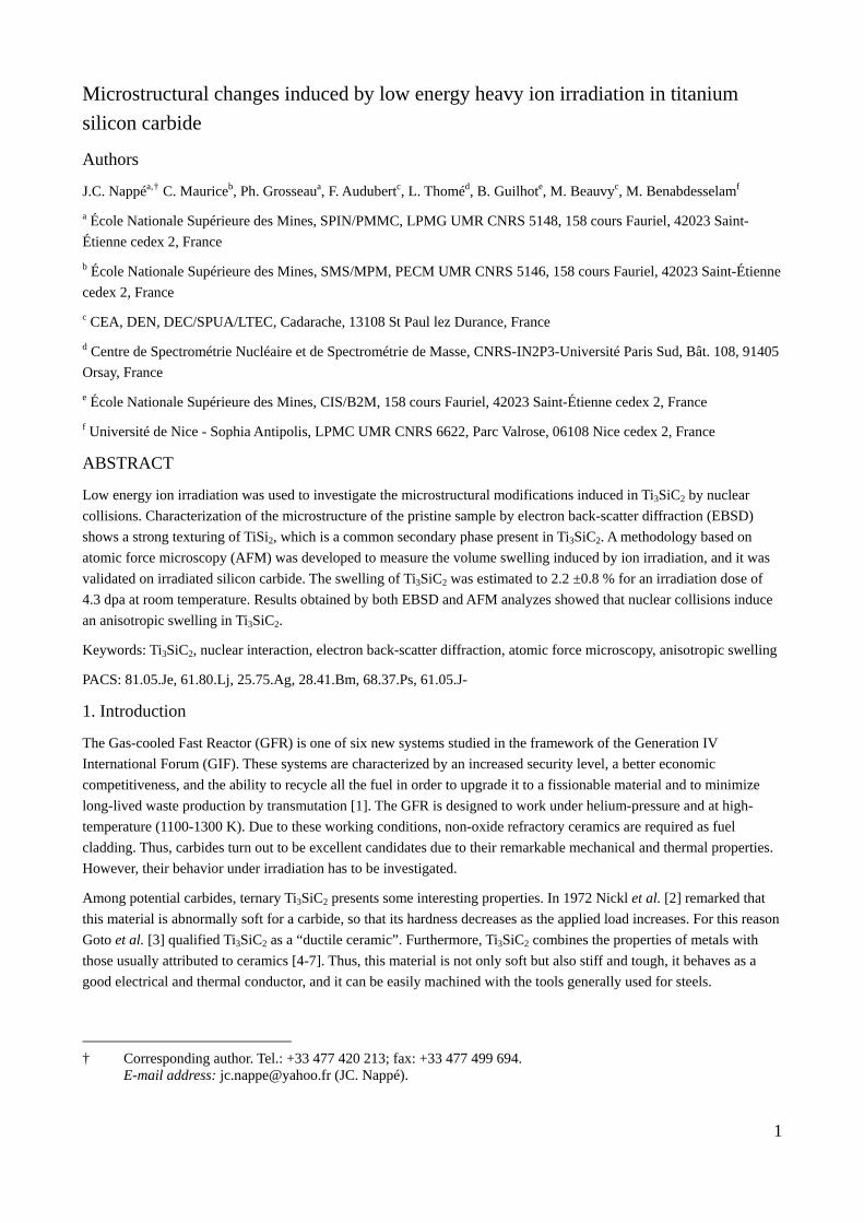
the same for all crystallites, inducing a large difference between the measured heights. So, it is likely that anisotropic swelling occurs, owing to the hexagonal close-packed structure of Ti3SiC2. Such an anisotropic swelling has already been observed in other materials presenting anisotropic structures [31,35,36]. Moreover, it has been shown that anisotropic swelling leads to the occurrence of significant stresses in the irradiated area, inducing fractures or microcracks at grain boundaries in polycrystalline materials [31,36]. Therefore, the anisotropic swelling would also explain what we previously thought to be an erosion phenomenon of the Ti3SiC2 grain boundaries [15]: as shown in Figure 8, mircocraks formed in the the grain boundaries of Ti3SiC2 irradiated at room temperature to 1019 m-2.
Figure 8: Back-scattered electrons micrograph of the microcrack formation on a sample irradiated at room temperature to 1019 m-2.
In this work, where other irradiation conditions were explored, microcrack formation was not observed in other samples. This result confirms the hypothesis that both the formation of microcracks and the microstructure revealing are due to anisotropic swelling of Ti3SiC2, and that, in the conditions investigated, the swelling of Ti3SiC2 decreases with decreasing ion fluence and/or with increasing irradiation temperature.
3.4. Ti3SiC2 swelling model
Several authors have discriminated different regimes of swelling in ceramics, which depend on the irradiation temperature [31,32]. At low temperatures, irradiation creates point defects or defect clusters, which lead to the amorphization of the material at high fluence. Defect creation induces a swelling, which increases with increasing fluence, and saturates when amorphization is completed (“amorphization regime”). Above the “critical amorphization temperature Tc”, temperature at which the damage recovery rate is equal to the damage rate, amorphization of the material does not occur, even at very high fluences. The value of Tc varies as a function of the nature of the material: for instance, 200 K for graphite [37], 200-250 K for Al2O3 [27], 400-650 K for SiC [38,39]. Thus, above Tc, the swelling increases with increasing fluence up to saturation, but it is only due to defect creation (“saturatable regime”). As the material does not become amorphous, the saturation swelling is much smaller than that measured in the amorphization regime, and it steadily decreases with increasing temperature. This decrease is generally attributed to the recombination of Frenkel pairs created in the collision cascades, which is enhanced at high temperature. Eventually, for temperatures high enough to allow vacancies to be significantly mobile, vacancy clusters can form and grow in cavities (or voids). In this “non-saturatable regime”, extended defects are the major cause of swelling, which becomes fluence dependent, and increases with increasing temperature. If Ti3SiC2 follows this model of swelling, it should be in the saturatable regime, whatever the irradiation temperature is. This assumption stems from the following statements:
9

(i) Nuclear collisions create defects in Ti3SiC2 without leading to amorphization [11,12,15], even for the highest studied dose (4.3 dpa), whereas SiC, which is in the amorphization regime at room temperature, becomes amorphous above 0.5 dpa. This suggests that Ti3SiC2 is not in the amorphization swelling regime;
(ii) No extended defects have been observed by transmission electron microscopy analyzes [8], even for the highest temperature (1223 K), suggesting that Ti3SiC2 is not in the non-saturatable regime;
(iii) The swelling decreases and increases respectively with the temperature and the dose (see Section 3.2.). This behavior is typical of the saturatable regime.
Therefore, the critical amorphization temperature of Ti3SiC2 would certainly be lower than room temperature, and the transition temperature between the saturatable and the non-saturatable regimes would be higher than 1223 K.
However, as Ti3SiC2 possesses some properties generally attributed to metals, and has also a behavior under electronic excitations similar to that of metals [8], it could follow another model. According to the literature, metals do not seem to become amorphous for very high dose [40,41], in the temperature range studied in this work. Moreover, the swelling of metals does not saturate, but increases linearly with the dose due to the agglomeration of point defects into extended defects, whatever the irradiation temperature. Eventually, a temperature increase usually induces an increase of the swelling up to a maximum for a critical temperature above which the swelling decreases [42]. Thus, considering that such a critical temperature is ever reached for irradiations at room temperature, the results presented in this work also match with this model, and complementary irradiations, such as irradiations at lower and higher temperatures, or creating more damage, are needed to better understand the swelling behavior of Ti3SiC2.
5. Conclusion
The first aim of this study was to confirm that the microstructure revealing, observed on Ti3SiC2 irradiated at room temperature with 4 MeV Au ions to 1019 m-2, depends on the crystallite orientation. This result was confirmed by combining AFM and EBSD observations that show similarities in the shape and size of both the revealed grains and the crystallites of the samples. Moreover, EBSD analyzes allowed the highlighting a hitherto unexpected result: the secondary phase TiSi2, present in the studied specimen, is highly textured. We conjecture that the formation of a liquid phase during the sample preparation could be the cause of this strong texturing.
The second goal of this work was to develop a methodology to estimate by AFM the volume swelling induced by ion irradiation. The method was validated with measurements performed on an irradiated SiC sample that match the result found in the literature. Using this method, we showed that Ti3SiC2 weakly swells at room temperature (2.2 ± 0.8 %) for an average irradiation dose of 4.3 dpa, whereas the swelling of SiC irradiated in the same conditions reaches 16.4 %. Furthermore, we showed that, in the temperature and damage range of our study, the higher the temperature or the lower the amount of damage, the lower the swelling of Ti3SiC2. However, complementary irradiations are needed to determine the swelling model applicable to Ti3SiC2, which can be either that implemented for ceramics or that implemented for metals.
Finally, by comparing the micrographs obtained by using both AFM and FEG-SEM, we showed that the microstructure revealing induced by irradiation is due to an anisotropic swelling of Ti3SiC2. Nevertheless, since neither microstructure revealing, nor crack formation have been observed on the sample irradiated at 1223 K to 1019 m-2, we can conclude that, from the swelling point of view, Ti3SiC2 seems to present interesting prospects for use as a cladd component of GFR.
Acknowledgement
The authors would like to greatly thank Isabelle Monnet from CIMAP (Caen, France) for numerous discussions about the swelling of irradiated materials. This work was partly funded by the French research group MATINEX.
10

References
[1] US.DoE, <http://nuclear.energy.gov/genIV/neGenIV1.html>. [2] J.J. Nickl, K.K. Schweitzer, P. Luxenberg, Gasphasenabscheidung im Systeme Ti-C-Si, J. Less-Common Metals 26 (1972) 335-353. [3] T. Goto, T. Hirai, Chemically vapor-deposited Ti3SiC2, Mater. Res. Bull. 22 (1987) 1195-1201. [4] M.W. Barsoum, The M(n+1)AX(n) phases: A new class of solids; Thermodynamically stable nanolaminates, Prog. Solid State Chem. 28 (2000) 201-281. [5] M.W. Barsoum, T. El-Raghy, The MAX phases: Unique new carbide and nitride materials - Ternary ceramics turn out to be surprisingly soft and machinable, yet also heat-tolerant, strong and lightweight, Am. Scientist 89 (2001) 334-343. [6] H.B. Zhang, Y.W. Bao, Y.C. Zhou, Current Status in Layered Ternary Carbide Ti3SiC2, a Review, J. Mater. Sci. Technol. 25 (2009) 1-38. [7] M.W. Barsoum, T. El-Raghy, Synthesis and characterization of a remarkable ceramic: Ti3SiC2, J. Am. Ceram. Soc. 79 (1996) 1953-1956. [8] J.C. Nappé, I. Monnet, Ph. Grosseau, F. Audubert, B. Guilhot, M. Beauvy, L. Thomé, M. Benabdesselam, Structural changes induced by heavy ion irradiation in titanium silicon carbide, Accepted for Publication in Journal of Nuclear Materials. [9] J.C. Nappé, I. Monnet, Ph. Grosseau, F. Audubert, B. Guilhot, M. Beauvy, M. Benabdesselam, Hill formation on titanium silicon carbide surface irradiated with swift heavy ions, Under Review. [10] K.R. Whittle, M.G. Blackford, R.D. Aughterson, S. Moricca, G.R. Lumpkin, D.P. Riley, N.J. Zaluzec, Radiation tolerance of Mn+1AXn phases, Ti3AlC2 and Ti3SiC2, Acta Mater. 58 (2010) 4362-4368. [11] M. Le Flem, X. Liu, S. Doriot, T. Cozzika, I. Monnet, Irradiation damage in Ti3(Si,Al)C2: a TEM investigation, Int. J. Appl. Ceram. Technol. 7 (2010) 766-775. [12] X. Liu, M. Le Flem, J.L. Béchade, F. Onimus, T. Cozzika, I. Monnet, XRD investigation of ion irradiated Ti3Si0.90Al0.10C2, Nucl. Instrum. Methods Phys. Res. Sect. B: Beam Interact. Mater. Atoms 268 (2010) 506-512. [13] M. Le Flem, X. Liu, S. Doriot, T. Cozzika, F. Onimus, J.L. Bechade, I. Monnet, Y. Zhou, Ti3(Si,Al)C2 for nuclear application: Investigation of irradiation effects induced by charged particles, Mechanical Properties and Performance of Engineering Ceramics and Composites IV, 30, Hoboken, NJ, USA, D. Singh & W.M. Kriven (2010) 189-198. [14] X. Liu, M. Le Flem, J.L. Béchade, I. Monnet, Nanoindentation investigation of heavy ion irradiated Ti3(Si,Al)C2, J. Nucl. Mater. 401 (2010) 149-153. [15] J.C. Nappé, Ph. Grosseau, F. Audubert, B. Guilhot, M. Beauvy, M. Benabdesselam, I. Monnet, Damages induced by heavy ions in titanium silicon carbide: Effects of nuclear and electronic interactions at room temperature, J. Nucl. Mater. 385 (2009) 304-307. [16] J.C. Nappé, Ph. Grosseau, B. Guilhot, F. Audubert, M. Beauvy, M. Benabdesselam, Heavy ions induced damages in Ti3SiC2: Effect of irradiation temperature, Mechanical Properties and Performance of Engineering Ceramics and Composites IV, 30, Hoboken, NJ, USA, D. Singh & W.M. Kriven (2010) 199-204. [17] J.F. Ziegler, <http://www.srim.org/>. [18] T. El-Raghy, M.W. Barsoum, Processing and mechanical properties of Ti3SiC2: I, reaction path and microstructure evolution, J. Am. Ceram. Soc. 82 (1999) 2849-2854. [19] H. Li, D. Chen, J. Zhou, J.H. Zhao, L.H. He, Synthesis of Ti3SiC2 by pressureless sintering of the elemental powders in vacuum, Mater. Lett. 58 (2004) 1741-1744. [20] F. Sato, J.F. Li, R. Watanabe, Reaction synthesis of Ti3SiC2 from mixture of elemental powders, Mater. Trans. 41 (2000) 605-608. [21] F. Audubert, G. Abrivard, C. Tallaron, Characterizations of Ti3SiC2 as candidate for the structural materials for high temperature reactors, Proceedings of the 30th International Conference and Exposition on Advanced Ceramics and Composites, Cocoa Beach, FL, US, (2006).
11

[22] I.J. Shon, H.K. Park, H.C. Kim, J.K. Yoon, K.T. Hong, I.Y Ko, One-step synthesis and densification of nanostructured TiSi2-SiC composite from mechanically activated (TiC + 3Si) powders by high-frequency-induced heated combustion, Scr. Mater. 56 (2007) 665-668. [23] J. Morgiel, J. Lis, R. Pampuch, Microstructure of Ti3SiC2-based ceramics, Mater. Lett. 27 (1996) 85-89. [24] R. Radhakrishnan, J. J. Williams, M. Akinc, Synthesis and high-temperature stability of Ti3SiC2, J. Alloy. Compd. 285 (1999) 85-88. [25] W.G. Spitzer, G.K. Hubler, T.A. Kennedy, Properties of amorphous silicon produced by ion implantation: Thermal annealing, Nucl. Instrum. Methods Phys. Res. 209-210 (1983) 309-312. [26] J.S. Custer, M.O. Thompson, D.C. Jacobson, J.M. Poate, S. Roorda, W.C. Sinke, F. Spaepen, Density of amorphous Si, Appl. Phys. Lett. 64 (1994) 437-439. [27] S.J. Zinkle, G.P. Pells, Microstructure of Al2O3 and MgAl2O4 irradiated at low temperatures, J. Nucl. Mater. 253 (1998) 120-132. [28] M. Terasawa, T. Mitamura, L. Liu, H. Tsubakino, M. Niibe, Metal surface swelling by heavy charged particle irradiation, Nucl. Instrum. Methods Phys. Res. Sect. B: Beam Interact. Mater. Atoms 193 (2002) 329-335. [29] F. Harbsmeier, J. Conrad, W. Bolse, Generation and relief of mechanical stresses in ion irradiated SiC and SiO2, Nucl. Instrum. Methods Phys. Res. Sect. B: Beam Interact. Mater. Atoms 137 (1998) 505-510. [30] M. Beauvy, C. Dalmasso, C. Thiriet-Dodane, D. Simeone, D. Gosset, Damages in ceramics for nuclear waste transmutation by irradiation with swift heavy ions, Nucl. Instrum. Methods Phys. Res. Sect. B: Beam Interact. Mater. Atoms 242 (2006) 557-561. [31] F.W. Clinard Jr., G.F. Hurley, L.W. Hobbs, Neutron irradiation damage in MgO, Al2O3 and MgAl2O4 ceramics, J. Nucl. Mater. 108-109 (1982) 655-670. [32] L.L. Snead, T. Nozawa, Y. Katoh, T.S. Byun, S. Kondo, D.A. Petti, Handbook of SiC properties for fuel performance modeling, J. Nucl. Mater. 371 (2007) 329-377. [33] D. Gosset, M. Dollé, D. Simeone, G. Baldinozzi, L. Thomé, Structural behaviour of nearly stoichiometric ZrC under ion irradiation, Nucl. Instrum. Methods Phys. Res. Sect. B: Beam Interact. Mater. Atoms 266 (2008) 2801-2805. [34] L.L. Snead, S.J. Zinkle, J.C. Hay, M.C. Osborne, Amorphization of SiC under ion and neutron irradiation, Nucl. Instrum. Methods Phys. Res. Sect. B: Beam Interact. Mater. Atoms 141 (1998) 123-132. [35] D. Gosset, D. Simeone, D. Quirion, Neutron irradiation damage to boron carbide: X-ray diffraction analysis, J. Phys. IV 10 (2000) Pr10-55-63. [36] T. Yano, T. Iseki, Swelling and microstructure of AlN irradiated in a fast-reactor, J. Nucl. Mater. 203 (1993) 249-254. [37] H. Abe, H. Naramoto, A. Iwase, C. Kinoshita, Effect of damage cascades on the irradiation-induced amorphization in graphite, Nucl. Instrum. Methods Phys. Res. Sect. B: Beam Interact. Mater. Atoms 127-128 (1997) 681-684. [38] A. Heft, E. Wendler, T. Bachmann, E. Glaser, W. Wesch, Defect production and annealing in ion implanted silicon carbide, Mater. Sci. Eng. B: Solid State Mater. Adv. Technol. 29 (1995) 142-146. [39] W.J. Weber, L.M. Wang, The temperature dependence of ion-beam-induced amorphization in beta-SiC, Nucl. Instrum. Methods Phys. Res. Sect. B: Beam Interact. Mater. Atoms 106 (1995) 298-302. [40] C. David, B.K. Panigrahi, G. Amarendra, S. Abhaya, S. Balaji, A.K. Balamurugan, K.G.M. Nair, B. Viswanathan, C.S. Sundar, B. Raj, Void swelling in ion irradiated (15Ni-14Cr), Ti-modified stainless steel: A study using positron annihilation and step height measurements, Surf. Coat. Technol. 203 (2009) 2363-2366. [41] F. A. Garner, D. S. Gelles, H. Takahashi, S. Ohnuki, H. Kinoshita, B. A. Loomis, High swelling rates observed in neutron-irradiated V-Cr and V-Si binary alloys, J. Nucl. Mater. 191-194 (1992) 948-951. [42] A.F. Rowcliffe, A. Hishinuma, M.L. Grossbeck, S. Jitsukawa, Radiation effects at fusion reactor He : dpa ratios: Overview of US/Japan spectrally tailored experiments, J. Nucl. Mater. 179-181 (1991) 125-129.
12