Embed Size (px)
Citation preview
W9
1606
383
0111
A02
09/0
4
Modbus Advantys OTBRemote I/O
September 2004
Eng V1.1

2

Table of Contents
Safety Information . . . . . . . . . . . . . . . . . . . . . . . . . . . . . . . . . . . . 7
About the Book . . . . . . . . . . . . . . . . . . . . . . . . . . . . . . . . . . . . . . .9
Chapter 1 Introduction . . . . . . . . . . . . . . . . . . . . . . . . . . . . . . . . . . . . . . . .11At a Glance . . . . . . . . . . . . . . . . . . . . . . . . . . . . . . . . . . . . . . . . . . . . . . . . . . . . . 11About Advantys OTB. . . . . . . . . . . . . . . . . . . . . . . . . . . . . . . . . . . . . . . . . . . . . . 12Maximum hardware configuration . . . . . . . . . . . . . . . . . . . . . . . . . . . . . . . . . . . . 18Specific Functions of the Network Interface Module . . . . . . . . . . . . . . . . . . . . . . 21Communication Overview . . . . . . . . . . . . . . . . . . . . . . . . . . . . . . . . . . . . . . . . . . 22
Chapter 2 Installation. . . . . . . . . . . . . . . . . . . . . . . . . . . . . . . . . . . . . . . . . . 25At a Glance . . . . . . . . . . . . . . . . . . . . . . . . . . . . . . . . . . . . . . . . . . . . . . . . . . . . . 25Dimensions of the Network Interface Modules . . . . . . . . . . . . . . . . . . . . . . . . . . 26Dimensions for the Digital and Analog I/O Expansion Modules . . . . . . . . . . . . . 27How to Direct Mount on a Panel Surface . . . . . . . . . . . . . . . . . . . . . . . . . . . . . . 30Installation Preparation . . . . . . . . . . . . . . . . . . . . . . . . . . . . . . . . . . . . . . . . . . . . 32Mounting Positions for the Network Interface Module and the Expansion Modules. . . . . . . . . . . . . . . . . . . . . . . . . . . . . . . . . . . . . . . . . . . . . . . . . . . . . . . . . . . . . . 33
Assembly Precautions for an Island or a Panel in a Cabinet . . . . . . . . . . . . . . . 35Assembly of an Expansion Module to a Network Interface Module . . . . . . . . . . 36Disassembly of an Expansion Module and a Network Interface Module . . . . . . 39Removing a Terminal Block . . . . . . . . . . . . . . . . . . . . . . . . . . . . . . . . . . . . . . . . 40How to Install and Remove a Network Interface Module from a DIN Rail. . . . . . 41The DIN Rail . . . . . . . . . . . . . . . . . . . . . . . . . . . . . . . . . . . . . . . . . . . . . . . . . . . . 43
Chapter 3 Description, characteristics, and wiring of the OTB module .45At a Glance . . . . . . . . . . . . . . . . . . . . . . . . . . . . . . . . . . . . . . . . . . . . . . . . . . . . . 45Wiring Rules and Recommendations . . . . . . . . . . . . . . . . . . . . . . . . . . . . . . . . . 46Overview of the Network Interface Modules . . . . . . . . . . . . . . . . . . . . . . . . . . . . 51Physical Description of an Advantys OTB Network Interface Module. . . . . . . . . 52General Characteristics of the Network Interface Module. . . . . . . . . . . . . . . . . . 53I/O Characteristics of the Network Interface Module. . . . . . . . . . . . . . . . . . . . . . 55Wiring diagram of the network interface module. . . . . . . . . . . . . . . . . . . . . . . . . 60How to Connect the Power Supply . . . . . . . . . . . . . . . . . . . . . . . . . . . . . . . . . . . 61
3
Connection of the Field Bus or Network . . . . . . . . . . . . . . . . . . . . . . . . . . . . . . . 63
Chapter 4 Description, characteristics, and wiring of the expansionmodules . . . . . . . . . . . . . . . . . . . . . . . . . . . . . . . . . . . . . . . . . . . 65At a Glance . . . . . . . . . . . . . . . . . . . . . . . . . . . . . . . . . . . . . . . . . . . . . . . . . . . . . 65Overview of Digital I/O Modules. . . . . . . . . . . . . . . . . . . . . . . . . . . . . . . . . . . . . . 66Parts Description of Digital I/O Modules . . . . . . . . . . . . . . . . . . . . . . . . . . . . . . . 70Specifications for the Digital I/O Modules . . . . . . . . . . . . . . . . . . . . . . . . . . . . . . 72Digital I/O Module Wiring Schematics . . . . . . . . . . . . . . . . . . . . . . . . . . . . . . . . . 83Overview of Analog I/O Modules . . . . . . . . . . . . . . . . . . . . . . . . . . . . . . . . . . . . . 93Parts Description of Analog I/O Modules. . . . . . . . . . . . . . . . . . . . . . . . . . . . . . . 94General Specifications for the Analog I/O Modules . . . . . . . . . . . . . . . . . . . . . . . 95Specifications for the Analog I/O Modules. . . . . . . . . . . . . . . . . . . . . . . . . . . . . . 96Analog I/O Modules Wiring Schematics. . . . . . . . . . . . . . . . . . . . . . . . . . . . . . . 100
Chapter 5 Modbus Network Interface of the OTB Module . . . . . . . . . . . 105At a Glance . . . . . . . . . . . . . . . . . . . . . . . . . . . . . . . . . . . . . . . . . . . . . . . . . . . . 105Description of the OTB Module Modbus Network Interface. . . . . . . . . . . . . . . . 106Modbus Field Bus Interface . . . . . . . . . . . . . . . . . . . . . . . . . . . . . . . . . . . . . . . . 108Network Node Address . . . . . . . . . . . . . . . . . . . . . . . . . . . . . . . . . . . . . . . . . . . 112Network Baud Rate . . . . . . . . . . . . . . . . . . . . . . . . . . . . . . . . . . . . . . . . . . . . . . 114Modbus Configuration . . . . . . . . . . . . . . . . . . . . . . . . . . . . . . . . . . . . . . . . . . . . 116Communication on a Modbus Network . . . . . . . . . . . . . . . . . . . . . . . . . . . . . . . 117Management of Island Behavior . . . . . . . . . . . . . . . . . . . . . . . . . . . . . . . . . . . . 120Expansion module identification codes . . . . . . . . . . . . . . . . . . . . . . . . . . . . . . . 124
Chapter 6 Application-Specific Functions . . . . . . . . . . . . . . . . . . . . . . . 125At a Glance . . . . . . . . . . . . . . . . . . . . . . . . . . . . . . . . . . . . . . . . . . . . . . . . . . . . 125Island Registers . . . . . . . . . . . . . . . . . . . . . . . . . . . . . . . . . . . . . . . . . . . . . . . . . 126Read Input Registers . . . . . . . . . . . . . . . . . . . . . . . . . . . . . . . . . . . . . . . . . . . . . 129Output Command Registers . . . . . . . . . . . . . . . . . . . . . . . . . . . . . . . . . . . . . . . 130Advantys OTB Module I/O Parameter Registers . . . . . . . . . . . . . . . . . . . . . . . . 131Expansion Module Discrete I/O Parameter Registers 214 to 599 . . . . . . . . . . . 132Expansion Module Analog I/O Parameter Registers 214 to 599 . . . . . . . . . . . . 135Specific Functions of the Advantys OTB Modules. . . . . . . . . . . . . . . . . . . . . . . 150Remote Fast Counter (RFC) Function Block . . . . . . . . . . . . . . . . . . . . . . . . . . . 152Fast Counter (RFC) Parameter Registers . . . . . . . . . . . . . . . . . . . . . . . . . . . . . 155Remote Very Fast Counter (RVFC) Function Block . . . . . . . . . . . . . . . . . . . . . 156Remote Very Fast Counter (RVFC) Parameter Registers . . . . . . . . . . . . . . . . . 169Remote Pulse Generator (RPLS) Function Block . . . . . . . . . . . . . . . . . . . . . . . 171Remote Pulse Width Modulator Function Block. . . . . . . . . . . . . . . . . . . . . . . . . 175Remote Pulse Generators (RPLS, RPWM) Parameter Registers . . . . . . . . . . . 179
Chapter 7 Software Installation . . . . . . . . . . . . . . . . . . . . . . . . . . . . . . . . 181Advantys Configuration Tool . . . . . . . . . . . . . . . . . . . . . . . . . . . . . . . . . . . . . . . 181
4

Chapter 8 Diagnostics of the Advantys OTB Island . . . . . . . . . . . . . . . .183Overview . . . . . . . . . . . . . . . . . . . . . . . . . . . . . . . . . . . . . . . . . . . . . . . . . . . . . . 183Indicator Lights (LEDs) . . . . . . . . . . . . . . . . . . . . . . . . . . . . . . . . . . . . . . . . . . . 184OTB Island Diagnostics Registers. . . . . . . . . . . . . . . . . . . . . . . . . . . . . . . . . . . 186Behavior in the Event of a Fault . . . . . . . . . . . . . . . . . . . . . . . . . . . . . . . . . . . . 190
Chapter 9 Island Registers Table . . . . . . . . . . . . . . . . . . . . . . . . . . . . . . .191Registers Table (mapping) for Modbus Advantys OTB Module . . . . . . . . . . . . 191
Appendices . . . . . . . . . . . . . . . . . . . . . . . . . . . . . . . . . . . . . . . . . . . . . 205At a Glance . . . . . . . . . . . . . . . . . . . . . . . . . . . . . . . . . . . . . . . . . . . . . . . . . . . . 205
Appendix A IEC Symbols . . . . . . . . . . . . . . . . . . . . . . . . . . . . . . . . . . . . . . .207Glossary of Symbols . . . . . . . . . . . . . . . . . . . . . . . . . . . . . . . . . . . . . . . . . . . . . 207
Glossary . . . . . . . . . . . . . . . . . . . . . . . . . . . . . . . . . . . . . . . . . . . . . 209
Index . . . . . . . . . . . . . . . . . . . . . . . . . . . . . . . . . . . . . . . . . . . . . 225
5

6

§
Safety InformationImportant Information
NOTICE Read these instructions carefully, and look at the equipment to become familiar withthe device before trying to install, operate, or maintain it. The following specialmessages may appear throughout this documentation or on the equipment to warnof potential hazards or to call attention to information that clarifies or simplifies aprocedure.
DANGERDANGER indicates an imminently hazardous situation, which, if not avoided, will resultin death, serious injury, or equipment damage.
WARNINGWARNING indicates a potentially hazardous situation, which, if not avoided, can resultin death, serious injury, or equipment damage.
CAUTIONCAUTION indicates a potentially hazardous situation, which,can result inpersonal injury or equipment damage.
The addition of this symbol to a Danger or Warning safety label indicatesthat an electrical hazard exists, which will result in personal injury if theinstructions are not followed.This is the safety alert symbol. It is used to alert you to potential personalinjury hazards. Obey all safety messages that follow this symbol to avoidpossible injury or death.
W9 1606383 01 11 A02 09/04 7

Safety Information
PLEASE NOTE Electrical equipment should be serviced only by qualified personnel. No responsi-bility is assumed by Schneider Electric for any consequences arising out of the useof this material. This document is not intended as an instruction manual for untrainedpersons.© 2004 Schneider Electric. All Rights Reserved.
8 W9 1606383 01 11 A02 09/04
About the Book
At a Glance
Document Scope This guide contains the information necessary to install a Modbus Advantys OTBnetwork interface module.It has been designed to facilitate a rapid familiarization with the system, whileoptimizing the system's features with the most advanced technology available.This equipment's installation needs the relative communication protocol pre-requisites and should only be installed by qualified personnel. Special points andwarnings regarding safety are highlighted in the different chapters.The initial chapters aim to provide information for designers and fitters for installingthe mechanical and electrical part of the system. They describe the characteristicswhich are common to the whole Advantys OTB range and are not dependent on theselected communication protocol.The following chapters, from the "network interface" section, are specific to thecommunication protocol. They contain information on specific wiring for the networkinterface and all the necessary information for the software application programmer,and for the end user (diagnostics).
Chapter Subject dealt with
Introduction General introduction to the network interface module andexpansion modules
Description Software installation, dimensions, installation and assemblyof an island
Description, characteristics,and wiring of the AdvantysOTB module
Description, electrical and mechanical characteristics andwiring diagrams for the OTB module
Description, characteristicsand wiring of expansionmodules
Description, electrical and mechanical characteristics andwiring diagrams for expansion modules
W9 1606383 01 11 A02 09/04 9

About the Book
User Comments We welcome your comments about this document. You can reach us by e-mail [email protected]
Advantys OTB moduleModbus network interface
Introduction to the OTB module network interfaceReminders on the communication protocolManagement of behavior of the island on the network
Application-specific functions Description of application-specific functionsRemote I/O and specific function registers table
Software installation Software installation help
Advantys OTB islanddiagnostics
Description of hardware diagnosticsDescription of software diagnosticsHow to perform diagnostics in the event of a failure
Advantys OTB island registerstable
Description of the registers accessible for communication
Glossary AcronymsDefinitions.
Chapter Subject dealt with
10 W9 1606383 01 11 A02 09/04

W9 1606383 01 11 A02 09/04
1
IntroductionAt a Glance
Introduction This chapter provides an overview of the Advantys OTB network interface modules,the different expansion modules, the maximum configuration and the specificfunctions of the module, as well as a communication architecture.
What's in thisChapter?
This chapter contains the following topics:
Topic Page
About Advantys OTB 12
Maximum hardware configuration 18
Specific Functions of the Network Interface Module 21
Communication Overview 22
11

Introduction
About Advantys OTB
Introduction The Advantys OTB (Optimized Terminal Block) network interface module with built-in Inputs/Outputs is small in size. Its modularity, by adding I/O expansions, can beused to optimize an application by providing the necessary number of I/Os. TheAdvantys OTB module connects directly to a field bus or communication network.The available field buses or networks are as follows:
CANopen field bus: Module OTB1C0DM9LPModbus field bus: Module OTB1S0DM9LPEthernet communication network: Module OTB1E0DM9LP
The network interface module accepts up to 7 I/O expansion modules
12 W9 1606383 01 11 A02 09/04
Introduction
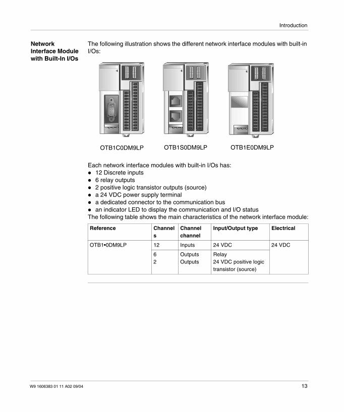
NetworkInterface Modulewith Built-In I/Os
The following illustration shows the different network interface modules with built-inI/Os:
Each network interface modules with built-in I/Os has:12 Discrete inputs6 relay outputs2 positive logic transistor outputs (source)a 24 VDC power supply terminala dedicated connector to the communication busan indicator LED to display the communication and I/O status
The following table shows the main characteristics of the network interface module:
Reference Channels
Channelchannel
Input/Output type Electrical
OTB1•0DM9LP 12 Inputs 24 VDC 24 VDC
62
OutputsOutputs
Relay24 VDC positive logictransistor (source)
OTB1S0DM9LP OTB1E0DM9LPOTB1C0DM9LP
W9 1606383 01 11 A02 09/04 13
Introduction
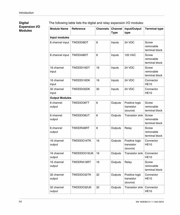
DigitalExpansion I/OModules
The following table lists the digital and relay expansion I/O modules:
Module Name Reference Channels ChannelType
Input/Outputtype
Terminal type
Input modules
8 channel input TWDDDI8DT 8 Inputs 24 VDC Screwremovableterminal block
8 channel input TWDDAI8DT 8 Inputs 120 VAC Screwremovableterminal block
16 channelinput
TWDDDI16DT 16 Inputs 24 VDC Screwremovableterminal block
16 channelinput
TWDDDI16DK 16 Inputs 24 VDC ConnectorHE10
32 channelinput
TWDDDI32DK 32 Inputs 24 VDC ConnectorHE10
Output Modules
8 channeloutput
TWDDDO8TT 8 Outputs Positive logictransistor(source)
Screwremovableterminal block
8 channeloutput
TWDDDO8UT 8 Outputs Transistor sink Screwremovableterminal block
8 channeloutput
TWDDRA8RT 8 Outputs Relay Screwremovableterminal block
16 channeloutput
TWDDDO16TK 16 Outputs Positive logictransistor(source)
ConnectorHE10
16 channeloutput
TWDDDDO16UK 16 Outputs Transistor sink ConnectorHE10
16 channeloutput
TWDDRA16RT 16 Outputs Relay Screwremovableterminal block
32 channeloutput
TWDDDO32TK 32 Outputs Positive logictransistor(source)
ConnectorHE10
32 channeloutput
TWDDDO32UK 32 Outputs Transistor sink ConnectorHE10
14 W9 1606383 01 11 A02 09/04

Introduction
Mixed modules
4 channel input/4 channeloutput
TWDDMM8DRT 4 Inputs 24 VDC Screwremovableterminal block
4 Outputs Relay
16 channelinput/8 channeloutput
TWDDMM24DRF 16 Inputs 24 VDC Spring non-removableterminal block
8 Outputs Relay
Module Name Reference Channels ChannelType
Input/Outputtype
Terminal type
W9 1606383 01 11 A02 09/04 15
Introduction
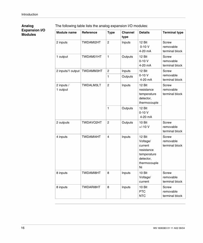
AnalogExpansion I/OModules
The following table lists the analog expansion I/O modules:
Module name Reference Type Channeltype
Details Terminal type
2 inputs TWDAMI2HT 2 Inputs 12 Bit0-10 V
4-20 mA
Screwremovableterminal block
1 output TWDAM01HT 1 Outputs 12 Bit0-10 V4-20 mA
Screwremovableterminal block
2 inputs/1 output TWDAMM3HT 2 Inputs 12 Bit0-10 V4-20 mA
Screwremovableterminal block
1 Outputs
2 inputs /1 output
TWDALM3LT 2 Inputs 12 Bitresistancetemperaturedetector,thermocouple
Screwremovableterminal block
1 Outputs 12 Bit0-10 V4-20 mA
2 outputs TWDAVO2HT 2 Outputs 10 Bit+/-10 V
Screwremovableterminal block
4 inputs TWDAMI4HT 4 Inputs 12 BitVoltage/currentresistancetemperaturedetector,thermocoupleNi
Screwremovableterminal block
8 inputs TWDAMI8HT 8 Inputs 10 BitVoltage/current
Screwremovableterminal block
8 inputs TWDARI8HT 8 Inputs 10 BitPTCNTC
Screwremovableterminal block
16 W9 1606383 01 11 A02 09/04
Introduction
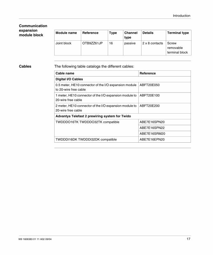
Communicationexpansionmodule block
Cables The following table catalogs the different cables:
Module name Reference Type Channeltype
Details Terminal type
Joint block OTB9ZZ61JP 16 passive 2 x 8 contacts Screwremovableterminal block
Cable name Reference
Digital I/O Cables
0.5 meter, HE10 connector of the I/O expansion moduleto 20-wire free cable
ABFT20E050
1 meter, HE10 connector of the I/O expansion module to20-wire free cable
ABFT20E100
2 meter, HE10 connector of the I/O expansion module to20-wire free cable
ABFT20E200
Advantys Telefast 2 prewiring system for Twido
TWDDDO16TK TWDDDO32TK compatible ABE7E16SPN20
ABE7E16SPN22
ABE7E16SRM20
TWDDDI16DK TWDDDI32DK compatible ABE7E16EPN20
W9 1606383 01 11 A02 09/04 17
Introduction
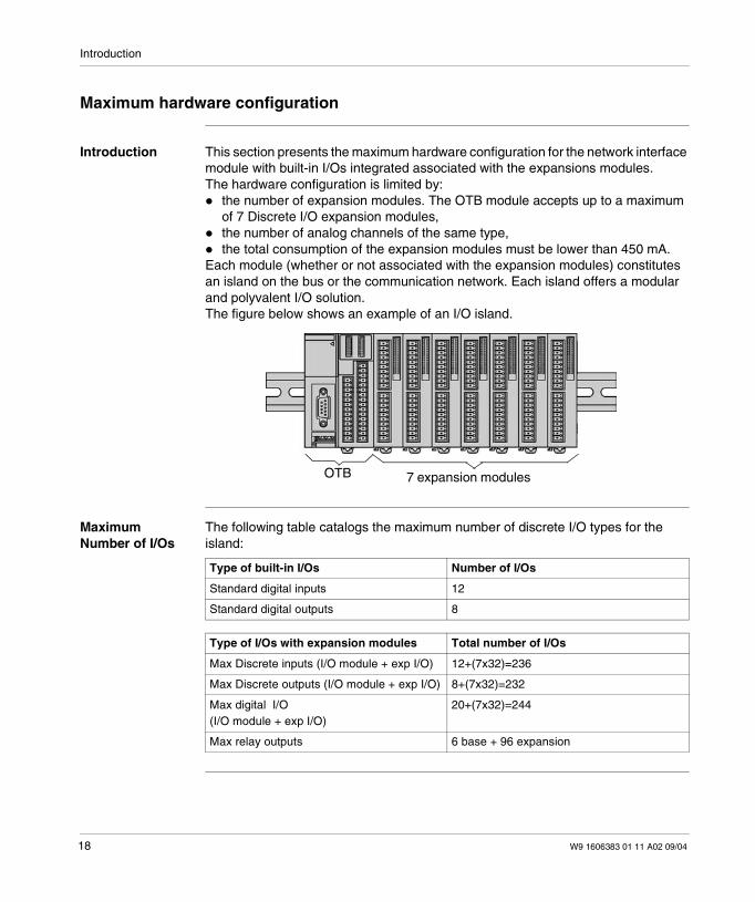
Maximum hardware configuration
Introduction This section presents the maximum hardware configuration for the network interfacemodule with built-in I/Os integrated associated with the expansions modules.The hardware configuration is limited by:
the number of expansion modules. The OTB module accepts up to a maximumof 7 Discrete I/O expansion modules,the number of analog channels of the same type,the total consumption of the expansion modules must be lower than 450 mA.
Each module (whether or not associated with the expansion modules) constitutesan island on the bus or the communication network. Each island offers a modularand polyvalent I/O solution.The figure below shows an example of an I/O island.
MaximumNumber of I/Os
The following table catalogs the maximum number of discrete I/O types for theisland:
OTB 7 expansion modules
Type of built-in I/Os Number of I/Os
Standard digital inputs 12
Standard digital outputs 8
Type of I/Os with expansion modules Total number of I/Os
Max Discrete inputs (I/O module + exp I/O) 12+(7x32)=236
Max Discrete outputs (I/O module + exp I/O) 8+(7x32)=232
Max digital I/O(I/O module + exp I/O)
20+(7x32)=244
Max relay outputs 6 base + 96 expansion
18 W9 1606383 01 11 A02 09/04

Introduction
MaximumNumber ofAnalog Channels
The following table catalogs the maximum number of analog channels by types forthe island:
Type of analog I/O Number of analog channels
Analog inputs 24
Analog outputs 24
W9 1606383 01 11 A02 09/04 19
Introduction
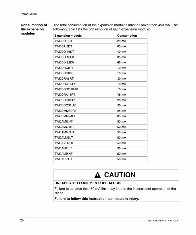
Consumption ofthe expansionmodules
The total consumption of the expansion modules must be lower than 450 mA. Thefollowing table lists the consumption of each expansion module:
Expansion module Consumption
TWDDDI8DT 25 mA
TWDDAI8DT 60 mA
TWDDDI16DT 40 mA
TWDDDI16DK 35 mA
TWDDDI32DK 65 mA
TWDDDO8TT 10 mA
TWDDDO8UT 10 mA
TWDDRA8RT 30 mA
TWDDDO16TK 10 mA
TWDDDDO16UK 10 mA
TWDDRA16RT 45 mA
TWDDDO32TK 20 mA
TWDDDO32UK 20 mA
TWDDMM8DRT 25 mA
TWDDMM24DRF 65 mA
TWDAMI2HT 50 mA
TWDAMO1HT 50 mA
TWDAMM3HT 50 mA
TWDALM3LT 50 mA
TWDAVO2HT 50 mA
TWDAMI4LT 50 mA
TWDAMI8HT 50 mA
TWDARI8HT 50 mA
CAUTIONUNEXPECTED EQUIPMENT OPERATION
Failure to observe the 450 mA limit may lead to the inconsistent operation of theisland.
Failure to follow this instruction can result in injury.
20 W9 1606383 01 11 A02 09/04

Introduction
Specific Functions of the Network Interface Module
Introduction By default, all I/Os of the network interface module are configured as Discrete I/Os.However, certain I/Os can be assigned to remote function blocks.
SpecificFunctions
The following table lists the specific functions of the network interface module:
Function Description
Fast counter: RFC 2 fast up/down counters: 5 kHz (1-phase)
Very fast counter: RVFC 2 very fast counters: Up/down counters - 20 kHz (2-phase)
Pulse generator: RPLS 2 pulse generatorsPulse output, maximum 7 kHz.
Pulse generator with pulsewidth modulation: RPWM
2 pulse generators with pulse width modulation RPWMpulse width modulation, maximum 7 kHz.
Programmable input filter Input filter time can be changed during configurationNo filtering or filtering at 3 ms or 12 ms
W9 1606383 01 11 A02 09/04 21
Introduction
Communication Overview
Introduction The Advantys OTB network interface modules are available for CANopen andModbus field buses, and for the Ethernet network. They are used to exchange datafrom the built-in I/Os and expansion module I/Os with the bus master or client.
Field bus ornetwork
A module with or without expansion constitutes an I/O island. The network interfacemodule manages data transfers between the island and the master or client, via thefield bus or network.
22 W9 1606383 01 11 A02 09/04
Introduction
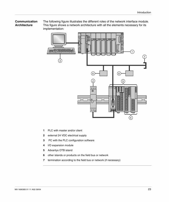
CommunicationArchitecture
The following figure illustrates the different roles of the network interface module.This figure shows a network architecture with all the elements necessary for itsimplementation:
1 PLC with master and/or client
2 external 24 VDC electrical supply
3 PC with the PLC configuration software
4 I/O expansion module
5 Advantys OTB island
6 other islands or products on the field bus or network
7 termination according to the field bus or network (if necessary)
W9 1606383 01 11 A02 09/04 23

Introduction
24 W9 1606383 01 11 A02 09/04
W9 1606383 01 11 A02 09/04
2
InstallationAt a Glance
Introduction This chapter provides dimensions, installation, and mounting instructions forAdvantys OTB network interface modules, and digital and analog expansion I/Omodules.
What's in thisChapter?
This chapter contains the following topics:
Topic Page
Dimensions of the Network Interface Modules 26
Dimensions for the Digital and Analog I/O Expansion Modules 27
How to Direct Mount on a Panel Surface 30
Installation Preparation 32
Mounting Positions for the Network Interface Module and the ExpansionModules
33
Assembly Precautions for an Island or a Panel in a Cabinet 35
Assembly of an Expansion Module to a Network Interface Module 36
Disassembly of an Expansion Module and a Network Interface Module 39
Removing a Terminal Block 40
How to Install and Remove a Network Interface Module from a DIN Rail 41
The DIN Rail 43
25
Installation
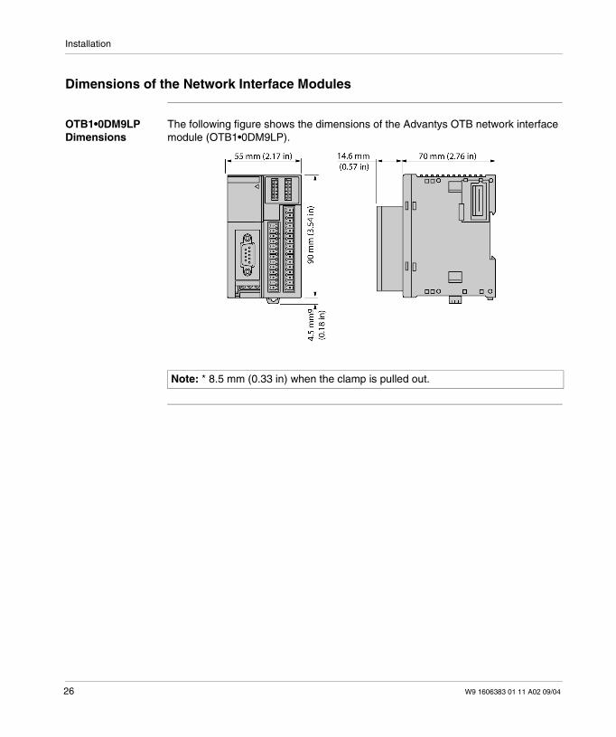
Dimensions of the Network Interface Modules
OTB1•0DM9LPDimensions
The following figure shows the dimensions of the Advantys OTB network interfacemodule (OTB1•0DM9LP).
Note: * 8.5 mm (0.33 in) when the clamp is pulled out.
26 W9 1606383 01 11 A02 09/04
Installation
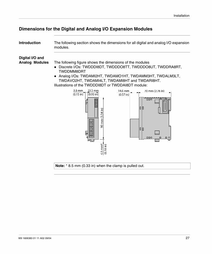
Dimensions for the Digital and Analog I/O Expansion Modules
Introduction The following section shows the dimensions for all digital and analog I/O expansionmodules.
Digital I/O andAnalog Modules The following figure shows the dimensions of the modules
Discrete I/Os: TWDDDI8DT, TWDDDO8TT, TWDDDO8UT, TWDDRA8RT,TWDDMM8DRTAnalog I/Os: TWDAMI2HT, TWDAMO1HT, TWDAMM3HT, TWDALM3LT,TWDAVO2HT, TWDAMI4LT, TWDAMI8HT and TWDARI8HT.
Illustrations of the TWDDDI8DT or TWDDAI8DT module:
Note: * 8.5 mm (0.33 in) when the clamp is pulled out.
W9 1606383 01 11 A02 09/04 27
Installation
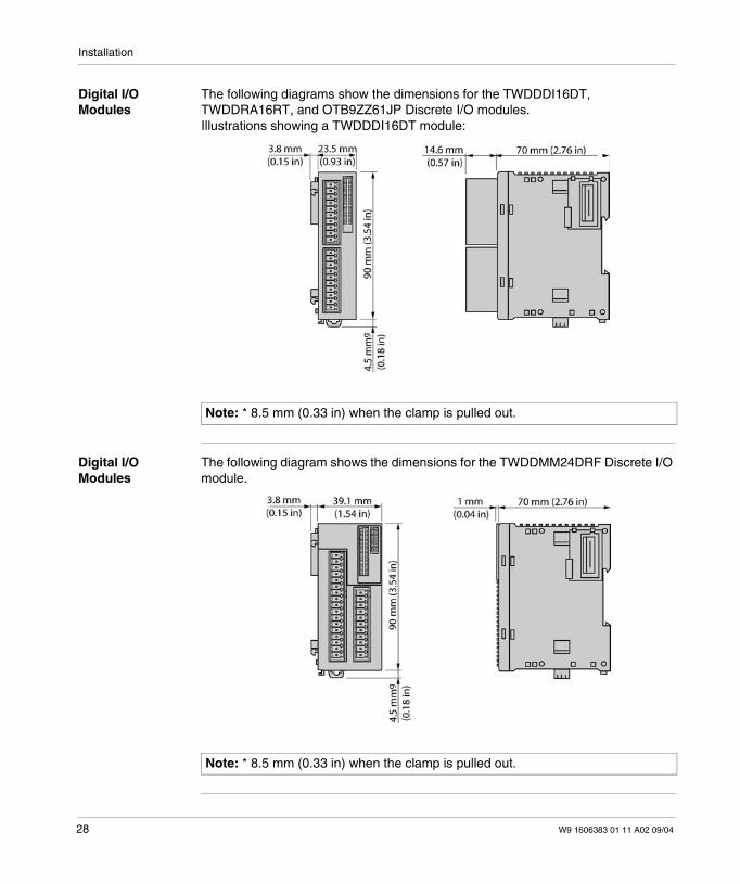
Digital I/OModules
The following diagrams show the dimensions for the TWDDDI16DT,TWDDRA16RT, and OTB9ZZ61JP Discrete I/O modules.Illustrations showing a TWDDDI16DT module:
Digital I/OModules
The following diagram shows the dimensions for the TWDDMM24DRF Discrete I/Omodule.
Note: * 8.5 mm (0.33 in) when the clamp is pulled out.
Note: * 8.5 mm (0.33 in) when the clamp is pulled out.
28 W9 1606383 01 11 A02 09/04
Installation
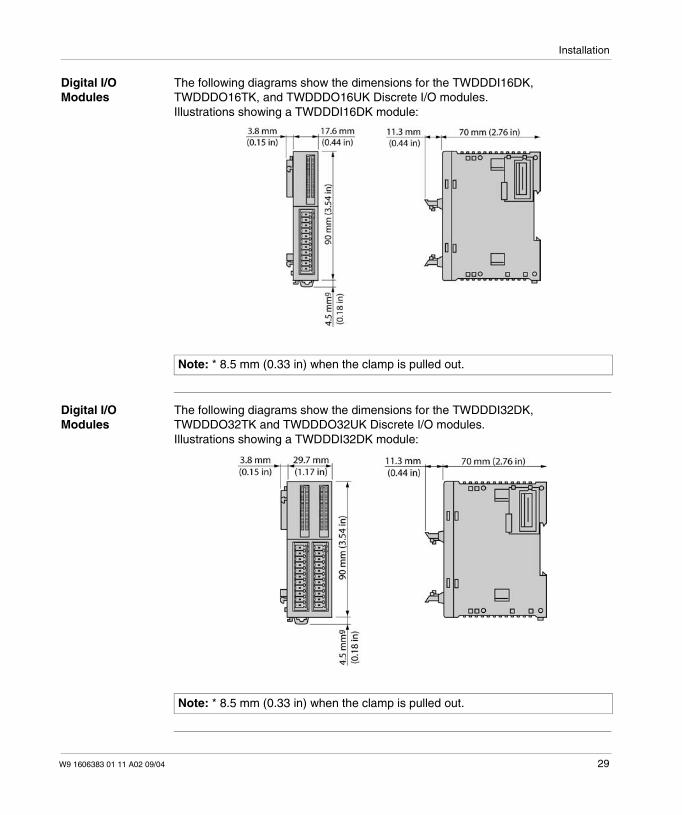
Digital I/OModules
The following diagrams show the dimensions for the TWDDDI16DK,TWDDDO16TK, and TWDDDO16UK Discrete I/O modules.Illustrations showing a TWDDDI16DK module:
Digital I/OModules
The following diagrams show the dimensions for the TWDDDI32DK,TWDDDO32TK and TWDDDO32UK Discrete I/O modules.Illustrations showing a TWDDDI32DK module:
Note: * 8.5 mm (0.33 in) when the clamp is pulled out.
Note: * 8.5 mm (0.33 in) when the clamp is pulled out.
W9 1606383 01 11 A02 09/04 29
Installation
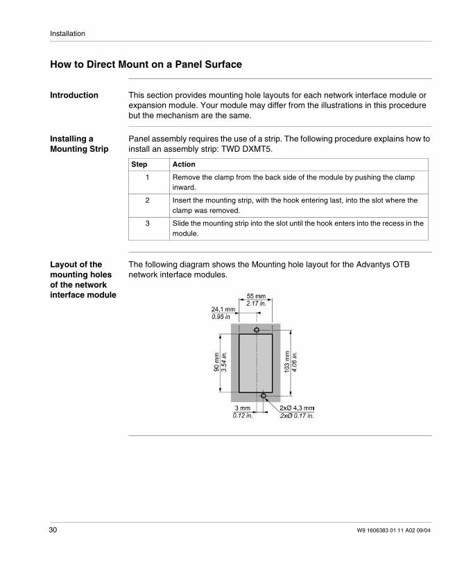
How to Direct Mount on a Panel Surface
Introduction This section provides mounting hole layouts for each network interface module orexpansion module. Your module may differ from the illustrations in this procedurebut the mechanism are the same.
Installing aMounting Strip
Panel assembly requires the use of a strip. The following procedure explains how toinstall an assembly strip: TWD DXMT5.
Layout of themounting holesof the networkinterface module
The following diagram shows the Mounting hole layout for the Advantys OTBnetwork interface modules.
Step Action
1 Remove the clamp from the back side of the module by pushing the clampinward.
2 Insert the mounting strip, with the hook entering last, into the slot where theclamp was removed.
3 Slide the mounting strip into the slot until the hook enters into the recess in themodule.
30 W9 1606383 01 11 A02 09/04
Installation
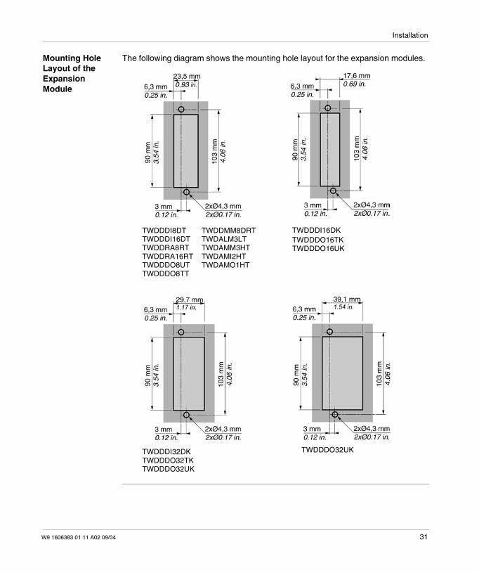
Mounting HoleLayout of theExpansionModule
The following diagram shows the mounting hole layout for the expansion modules.
TWDDDI8DTTWDDDI16DTTWDDRA8RTTWDDRA16RTTWDDDO8UTTWDDDO8TT
TWDDMM8DRTTWDALM3LTTWDAMM3HTTWDAMI2HTTWDAMO1HT
TWDDDI16DKTWDDDO16TKTWDDDO16UK
TWDDDI32DKTWDDDO32TKTWDDDO32UK
TWDDDO32UK
W9 1606383 01 11 A02 09/04 31
Installation
Installation Preparation
Introduction The following section provides information on installing network interface modulesand expansion I/O modules.
Before Starting Before installing network interface modules, read the Safety Information at thebegging of this book.
CAUTIONEQUIPMENT DAMAGE
Before removing an expansion module, power down the network interface module.Otherwise there is a risk of damaging the modules or the modules no longerworking correctly
Failure to follow this instruction can result in injury.
Note: All options and expansion I/O modules should be installed in the networkinterface module before installing an island on a DIN rail, on a mounting plate, orin a cabinet. The island should be removed from a DIN rail, a mounting plate or acabinet before disassembling the different modules.
32 W9 1606383 01 11 A02 09/04
Installation
Mounting Positions for the Network Interface Module and the ExpansionModules
Introduction This section shows the correct and incorrect mounting positions for all networkinterface modules and expansion I/O modules.
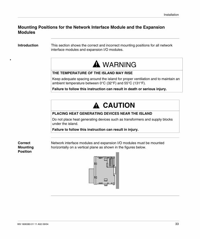
CorrectMountingPosition
Network interface modules and expansion I/O modules must be mountedhorizontally on a vertical plane as shown in the figures below.
WARNINGTHE TEMPERATURE OF THE ISLAND MAY RISE
Keep adequate spacing around the island for proper ventilation and to maintain anambient temperature between 0°C (32°F) and 55°C (131°F).
Failure to follow this instruction can result in death or serious injury.
CAUTIONPLACING HEAT GENERATING DEVICES NEAR THE ISLAND
Do not place heat generating devices such as transformers and supply blocksunder the island.
Failure to follow this instruction can result in injury.
W9 1606383 01 11 A02 09/04 33
Installation
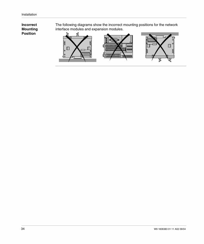
IncorrectMountingPosition
The following diagrams show the incorrect mounting positions for the networkinterface modules and expansion modules.
34 W9 1606383 01 11 A02 09/04
Installation
Assembly Precautions for an Island or a Panel in a Cabinet
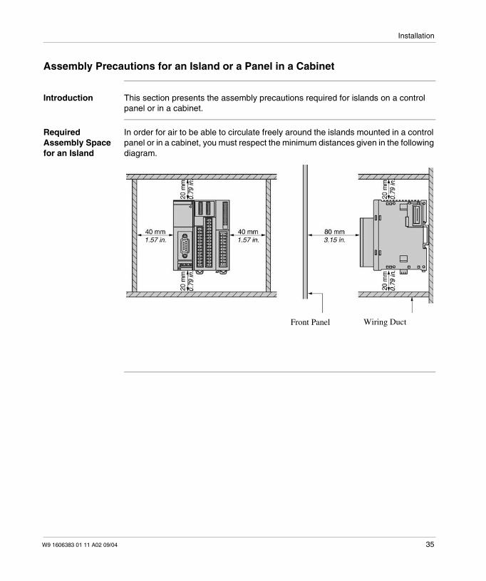
Introduction This section presents the assembly precautions required for islands on a controlpanel or in a cabinet.
RequiredAssembly Spacefor an Island
In order for air to be able to circulate freely around the islands mounted in a controlpanel or in a cabinet, you must respect the minimum distances given in the followingdiagram.
Front Panel Wiring Duct
W9 1606383 01 11 A02 09/04 35
Installation
Assembly of an Expansion Module to a Network Interface Module
Introduction This section shows how to assemble an expansion module to a network interfacemodule. Your network interface module or expansion module may differ to the onesshown in the illustrations for this procedure, but the mechanism remains the same.
CAUTIONUNEXPECTED EQUIPMENT OPERATION
If you change the hardware configuration of the island and do not update themaster or client application program, the island will no longer operate normally.The I/Os built into the network interface module will continue to operatenormally.
Failure to follow this instruction can result in injury.
36 W9 1606383 01 11 A02 09/04
Installation
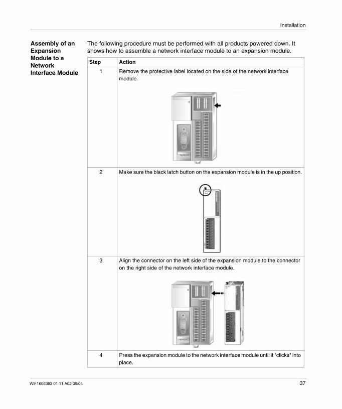
Assembly of anExpansionModule to aNetworkInterface Module
The following procedure must be performed with all products powered down. Itshows how to assemble a network interface module to an expansion module.
Step Action
1 Remove the protective label located on the side of the network interfacemodule.
2 Make sure the black latch button on the expansion module is in the up position.
3 Align the connector on the left side of the expansion module to the connectoron the right side of the network interface module.
4 Press the expansion module to the network interface module until it "clicks" intoplace.
W9 1606383 01 11 A02 09/04 37
Installation
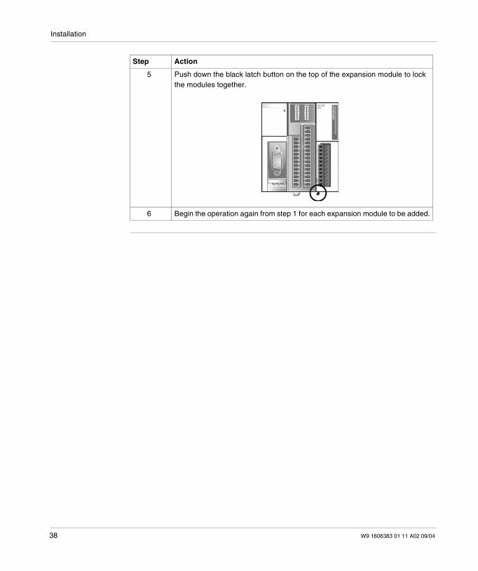
5 Push down the black latch button on the top of the expansion module to lockthe modules together.
6 Begin the operation again from step 1 for each expansion module to be added.
Step Action
38 W9 1606383 01 11 A02 09/04
Installation
Disassembly of an Expansion Module and a Network Interface Module
Introduction This section shows how to disassemble an expansion interface from a networkinterface module. Your network interface module or expansion module may differ tothe ones shown in the illustrations for this procedure, but the mechanism remainsthe same.
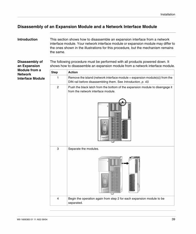
Disassembly ofan ExpansionModule from aNetworkInterface Module
The following procedure must be performed with all products powered down. Itshows how to disassemble an expansion module from a network interface module.
Step Action
1 Remove the island (network interface module + expansion module(s)) from theDIN rail before disassembling them. See Introduction, p. 43.
2 Push the black latch from the bottom of the expansion module to disengage itfrom the network interface module.
3 Separate the modules.
4 Begin the operation again from step 2 for each expansion module to beseparated.
W9 1606383 01 11 A02 09/04 39
Installation
Removing a Terminal Block
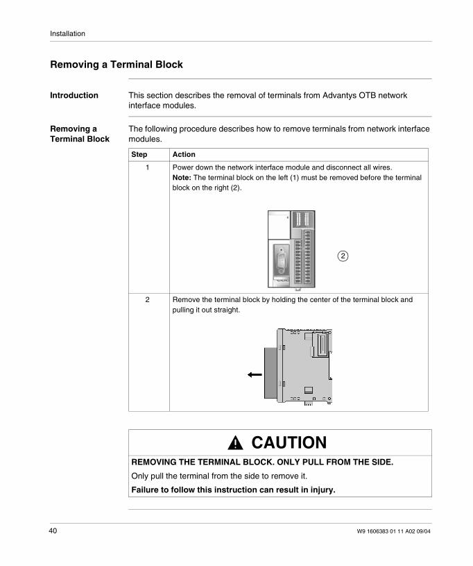
Introduction This section describes the removal of terminals from Advantys OTB networkinterface modules.
Removing aTerminal Block
The following procedure describes how to remove terminals from network interfacemodules.
Step Action
1 Power down the network interface module and disconnect all wires.Note: The terminal block on the left (1) must be removed before the terminalblock on the right (2).
2 Remove the terminal block by holding the center of the terminal block andpulling it out straight.
CAUTIONREMOVING THE TERMINAL BLOCK. ONLY PULL FROM THE SIDE.
Only pull the terminal from the side to remove it.
Failure to follow this instruction can result in injury.
2
40 W9 1606383 01 11 A02 09/04
Installation
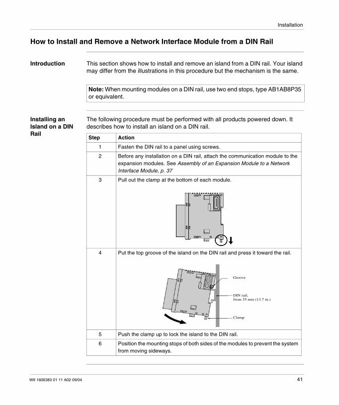
How to Install and Remove a Network Interface Module from a DIN Rail
Introduction This section shows how to install and remove an island from a DIN rail. Your islandmay differ from the illustrations in this procedure but the mechanism is the same.
Installing anIsland on a DINRail
The following procedure must be performed with all products powered down. Itdescribes how to install an island on a DIN rail.
Note: When mounting modules on a DIN rail, use two end stops, type AB1AB8P35or equivalent.
Step Action
1 Fasten the DIN rail to a panel using screws.
2 Before any installation on a DIN rail, attach the communication module to theexpansion modules. See Assembly of an Expansion Module to a NetworkInterface Module, p. 37
3 Pull out the clamp at the bottom of each module.
4 Put the top groove of the island on the DIN rail and press it toward the rail.
5 Push the clamp up to lock the island to the DIN rail.
6 Position the mounting stops of both sides of the modules to prevent the systemfrom moving sideways.
Groove
DIN rail,
Clamp
from 35 mm (13.7 in.)
W9 1606383 01 11 A02 09/04 41
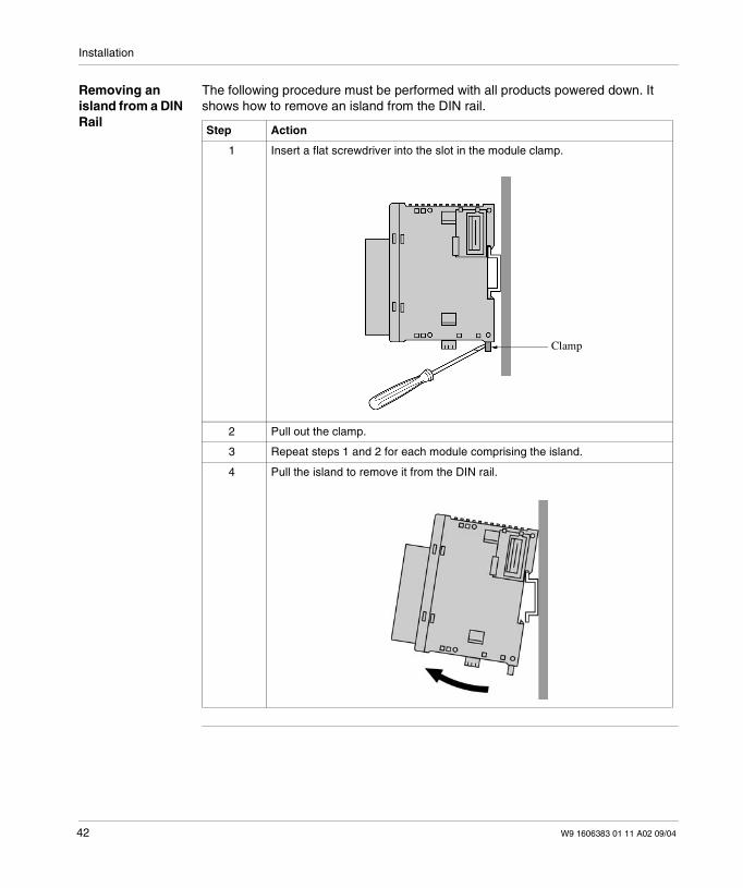
Installation
Removing anisland from a DINRail
The following procedure must be performed with all products powered down. Itshows how to remove an island from the DIN rail.
Step Action
1 Insert a flat screwdriver into the slot in the module clamp.
2 Pull out the clamp.
3 Repeat steps 1 and 2 for each module comprising the island.
4 Pull the island to remove it from the DIN rail.
Clamp
42 W9 1606383 01 11 A02 09/04
Installation
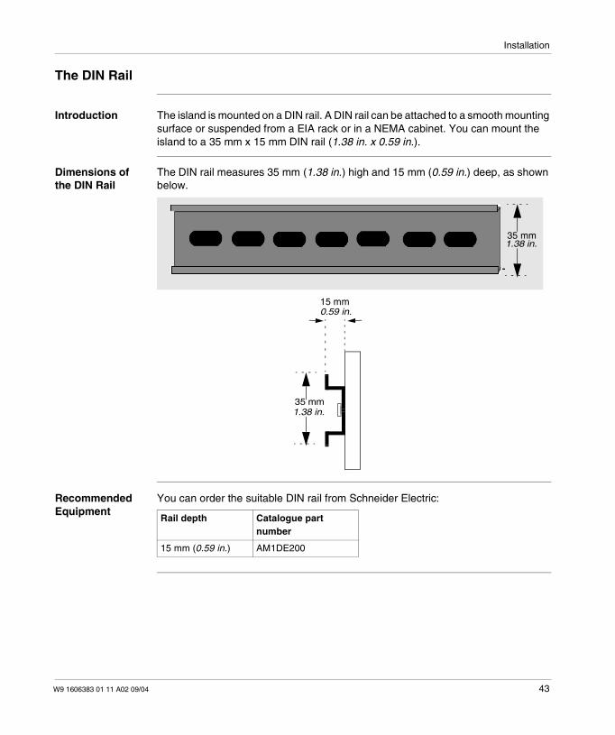
The DIN Rail
Introduction The island is mounted on a DIN rail. A DIN rail can be attached to a smooth mountingsurface or suspended from a EIA rack or in a NEMA cabinet. You can mount theisland to a 35 mm x 15 mm DIN rail (1.38 in. x 0.59 in.).
Dimensions ofthe DIN Rail
The DIN rail measures 35 mm (1.38 in.) high and 15 mm (0.59 in.) deep, as shownbelow.
RecommendedEquipment
You can order the suitable DIN rail from Schneider Electric:
35 mm
15 mm
35 mm1.38 in.
0.59 in.
1.38 in.
Rail depth Catalogue partnumber
15 mm (0.59 in.) AM1DE200
W9 1606383 01 11 A02 09/04 43

Installation
44 W9 1606383 01 11 A02 09/04

W9 1606383 01 11 A02 09/04
3
Description, characteristics, andwiring of the OTB moduleAt a Glance
Introduction This chapter describes the wiring rules and recommendations, overviews, partreferences, characteristics and wiring diagrams for the Advantys OTB networkinterface module.
What's in thisChapter?
This chapter contains the following topics:
Topic Page
Wiring Rules and Recommendations 46
Overview of the Network Interface Modules 51
Physical Description of an Advantys OTB Network Interface Module 52
General Characteristics of the Network Interface Module 53
I/O Characteristics of the Network Interface Module 55
Wiring diagram of the network interface module 60
How to Connect the Power Supply 61
Connection of the Field Bus or Network 63
45
Description, characteristics, and wiring of the OTB module
Wiring Rules and Recommendations
Introduction There are several rules that must be followed when wiring a module or networkinterface. Recommendations, when needed, are provided on how to comply with therules.
DANGERELECTRIC SHOCK
Be sure to remove ALL power from ALL devices before connecting ordisconnecting inputs or outputs to any terminal or installing or removing anyhardware.Make sure you have COMPLETELY powered down ALL devices beforeconnecting or disconnecting the bus or network.
Failure to follow this instruction will result in death or serious injury.
WARNINGUNEXPECTED EQUIPMENT OPERATION
If outputs should fail, outputs may remain on or off. Where personnel and orequipment hazards exist, use an appropriate hard-wired safety system.
Failure to follow this instruction can result in death or serious injury.
46 W9 1606383 01 11 A02 09/04

Description, characteristics, and wiring of the OTB module
Rules Each connector terminal accepts up to two wires fitted with cable ends or tags,
with sections between 0.08 mm2 and 0.75 mm2, (0.12 10-3 in.2 and 1.16 10-3 in.2
)Output module fusing is the responsibility of the user. It is not within the OTBnetwork interface module itself. Select a fuse appropriate for the load with respectto the electrical codes.Depending on the load, a protection circuit may be needed for relay outputs onmodules.
The power supply wire should be between 0.33 mm2 and 0.75 mm2 (0.51 10-
3 in.2 and 1.16 10-3 in.2 ). Use the shortest wire length possible.
The grounding wire should be 1.50 mm2 (2.3 10-3 in.2).Be sure to connect the grounding wire to a proper ground.Power supply wires routed inside the panel must be kept separate from I/O andcommunication wiring. Route wiring in separate cable ducting.Take care when wiring output modules that are designed to work as either sourceor sink. Incorrect wiring can cause equipment damage.Make sure that the operating conditions and environments are within thespecification values.Use proper wire size to meet voltage and current requirements.Fit cable ends to the cables.
W9 1606383 01 11 A02 09/04 47
Description, characteristics, and wiring of the OTB module
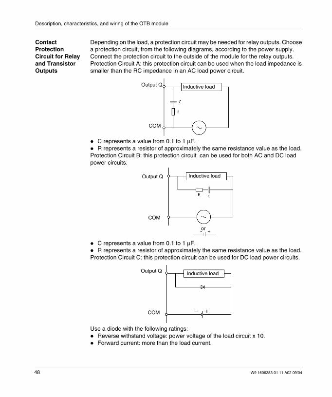
ContactProtectionCircuit for Relayand TransistorOutputs
Depending on the load, a protection circuit may be needed for relay outputs. Choosea protection circuit, from the following diagrams, according to the power supply.Connect the protection circuit to the outside of the module for the relay outputs.Protection Circuit A: this protection circuit can be used when the load impedance issmaller than the RC impedance in an AC load power circuit.
C represents a value from 0.1 to 1 µF.R represents a resistor of approximately the same resistance value as the load.
Protection Circuit B: this protection circuit can be used for both AC and DC loadpower circuits.
C represents a value from 0.1 to 1 µF.R represents a resistor of approximately the same resistance value as the load.
Protection Circuit C: this protection circuit can be used for DC load power circuits.
Use a diode with the following ratings:Reverse withstand voltage: power voltage of the load circuit x 10.Forward current: more than the load current.
Inductive loadOutput Q
COM
Output Q
COM
or +-
Inductive load
Output Q
COM
Inductive load
48 W9 1606383 01 11 A02 09/04
Description, characteristics, and wiring of the OTB module
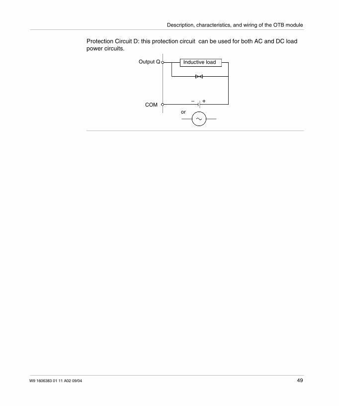
Protection Circuit D: this protection circuit can be used for both AC and DC loadpower circuits.
Output Q
COMor
Inductive load
W9 1606383 01 11 A02 09/04 49
Description, characteristics, and wiring of the OTB module
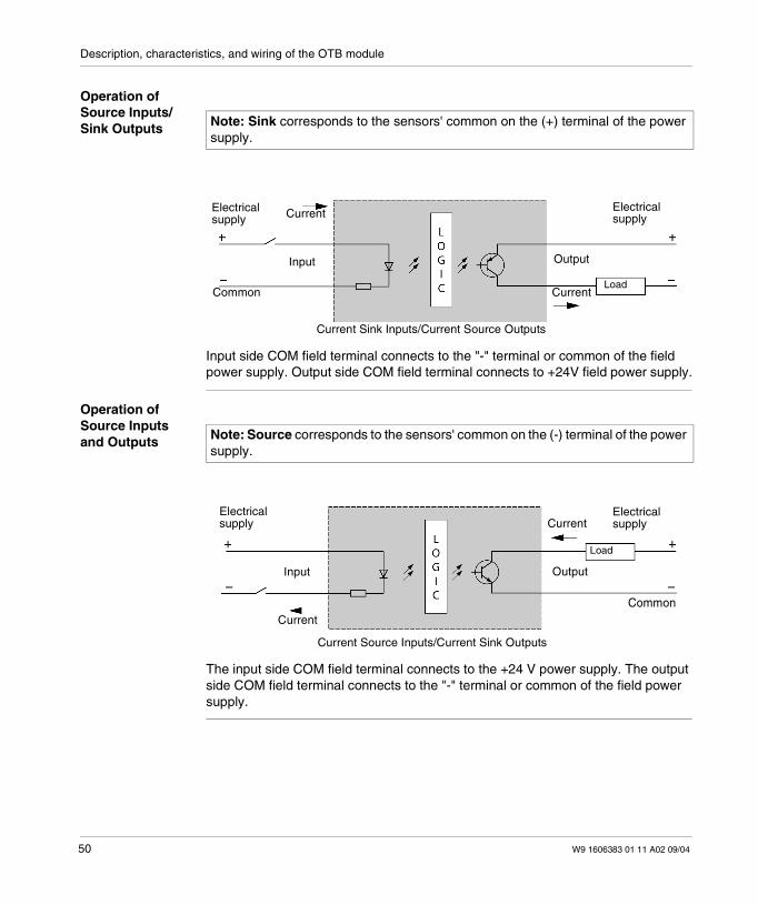
Operation ofSource Inputs/Sink Outputs
Input side COM field terminal connects to the "-" terminal or common of the fieldpower supply. Output side COM field terminal connects to +24V field power supply.
Operation ofSource Inputsand Outputs
The input side COM field terminal connects to the +24 V power supply. The outputside COM field terminal connects to the "-" terminal or common of the field powersupply.
Note: Sink corresponds to the sensors' common on the (+) terminal of the powersupply.
Current
LoadCurrent
OutputInput
Electricalsupply
Current Sink Inputs/Current Source Outputs
Electricalsupply
Common
Note: Source corresponds to the sensors' common on the (-) terminal of the powersupply.
Current
Load
Common
Current
OutputInput
Electricalsupply
Current Source Inputs/Current Sink Outputs
Electricalsupply
50 W9 1606383 01 11 A02 09/04
Description, characteristics, and wiring of the OTB module
Overview of the Network Interface Modules
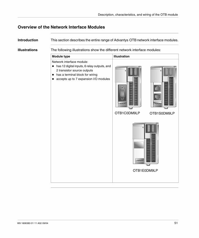
Introduction This section describes the entire range of Advantys OTB network interface modules.
Illustrations The following illustrations show the different network interface modules:
Module type Illustration
Network interface module:has 12 digital inputs, 6 relay outputs, and2 transistor source outputshas a terminal block for wiringaccepts up to 7 expansion I/O modules
OTB1C0DM9LP OTB1S0DM9LP
OTB1E0DM9LP
W9 1606383 01 11 A02 09/04 51
Description, characteristics, and wiring of the OTB module
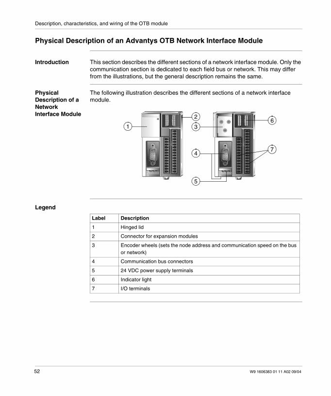
Physical Description of an Advantys OTB Network Interface Module
Introduction This section describes the different sections of a network interface module. Only thecommunication section is dedicated to each field bus or network. This may differfrom the illustrations, but the general description remains the same.
PhysicalDescription of aNetworkInterface Module
The following illustration describes the different sections of a network interfacemodule.
Legend
1
2
3
4
5
6
7
Label Description
1 Hinged lid
2 Connector for expansion modules
3 Encoder wheels (sets the node address and communication speed on the busor network)
4 Communication bus connectors
5 24 VDC power supply terminals
6 Indicator light
7 I/O terminals
52 W9 1606383 01 11 A02 09/04
Description, characteristics, and wiring of the OTB module
General Characteristics of the Network Interface Module
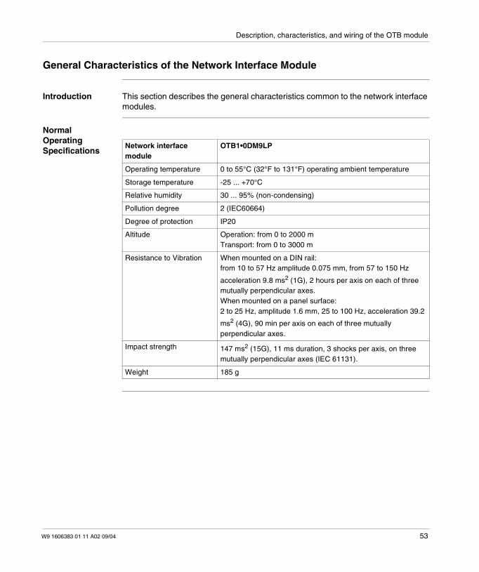
Introduction This section describes the general characteristics common to the network interfacemodules.
NormalOperatingSpecifications
Network interfacemodule
OTB1•0DM9LP
Operating temperature 0 to 55°C (32°F to 131°F) operating ambient temperature
Storage temperature -25 ... +70°C
Relative humidity 30 ... 95% (non-condensing)
Pollution degree 2 (IEC60664)
Degree of protection IP20
Altitude Operation: from 0 to 2000 mTransport: from 0 to 3000 m
Resistance to Vibration When mounted on a DIN rail:from 10 to 57 Hz amplitude 0.075 mm, from 57 to 150 Hz
acceleration 9.8 ms2 (1G), 2 hours per axis on each of threemutually perpendicular axes.When mounted on a panel surface:2 to 25 Hz, amplitude 1.6 mm, 25 to 100 Hz, acceleration 39.2
ms2 (4G), 90 min per axis on each of three mutuallyperpendicular axes.
Impact strength 147 ms2 (15G), 11 ms duration, 3 shocks per axis, on threemutually perpendicular axes (IEC 61131).
Weight 185 g
W9 1606383 01 11 A02 09/04 53
Description, characteristics, and wiring of the OTB module
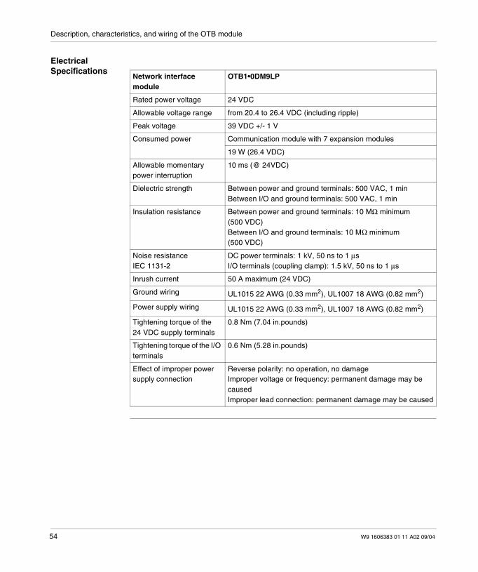
ElectricalSpecifications
Network interfacemodule
OTB1•0DM9LP
Rated power voltage 24 VDC
Allowable voltage range from 20.4 to 26.4 VDC (including ripple)
Peak voltage 39 VDC +/- 1 V
Consumed power Communication module with 7 expansion modules
19 W (26.4 VDC)
Allowable momentarypower interruption
10 ms (@ 24VDC)
Dielectric strength Between power and ground terminals: 500 VAC, 1 minBetween I/O and ground terminals: 500 VAC, 1 min
Insulation resistance Between power and ground terminals: 10 MΩ minimum(500 VDC)Between I/O and ground terminals: 10 MΩ minimum(500 VDC)
Noise resistanceIEC 1131-2
DC power terminals: 1 kV, 50 ns to 1 µsI/O terminals (coupling clamp): 1.5 kV, 50 ns to 1 µs
Inrush current 50 A maximum (24 VDC)
Ground wiring UL1015 22 AWG (0.33 mm2), UL1007 18 AWG (0.82 mm2)
Power supply wiring UL1015 22 AWG (0.33 mm2), UL1007 18 AWG (0.82 mm2)
Tightening torque of the24 VDC supply terminals
0.8 Nm (7.04 in.pounds)
Tightening torque of the I/Oterminals
0.6 Nm (5.28 in.pounds)
Effect of improper powersupply connection
Reverse polarity: no operation, no damageImproper voltage or frequency: permanent damage may becausedImproper lead connection: permanent damage may be caused
54 W9 1606383 01 11 A02 09/04
Description, characteristics, and wiring of the OTB module
I/O Characteristics of the Network Interface Module
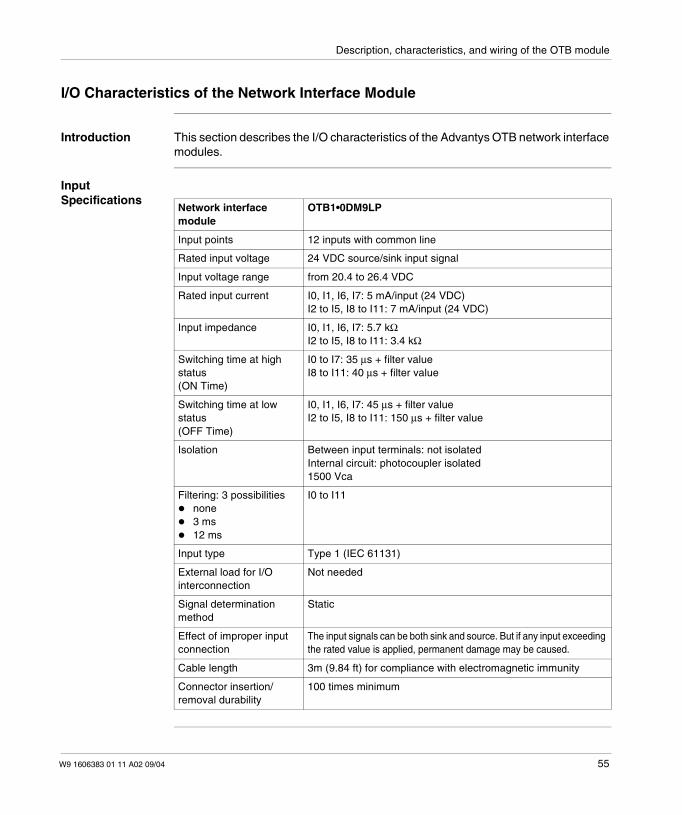
Introduction This section describes the I/O characteristics of the Advantys OTB network interfacemodules.
InputSpecifications
Network interfacemodule
OTB1•0DM9LP
Input points 12 inputs with common line
Rated input voltage 24 VDC source/sink input signal
Input voltage range from 20.4 to 26.4 VDC
Rated input current I0, I1, I6, I7: 5 mA/input (24 VDC)I2 to I5, I8 to I11: 7 mA/input (24 VDC)
Input impedance I0, I1, I6, I7: 5.7 kΩI2 to I5, I8 to I11: 3.4 kΩ
Switching time at highstatus(ON Time)
I0 to I7: 35 µs + filter valueI8 to I11: 40 µs + filter value
Switching time at lowstatus(OFF Time)
I0, I1, I6, I7: 45 µs + filter valueI2 to I5, I8 to I11: 150 µs + filter value
Isolation Between input terminals: not isolatedInternal circuit: photocoupler isolated1500 Vca
Filtering: 3 possibilitiesnone3 ms12 ms
I0 to I11
Input type Type 1 (IEC 61131)
External load for I/Ointerconnection
Not needed
Signal determinationmethod
Static
Effect of improper inputconnection
The input signals can be both sink and source. But if any input exceedingthe rated value is applied, permanent damage may be caused.
Cable length 3m (9.84 ft) for compliance with electromagnetic immunity
Connector insertion/removal durability
100 times minimum
W9 1606383 01 11 A02 09/04 55
Description, characteristics, and wiring of the OTB module
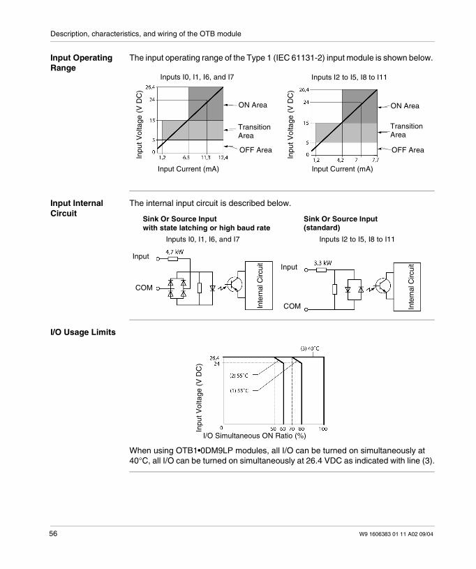
Input OperatingRange
The input operating range of the Type 1 (IEC 61131-2) input module is shown below.
Input InternalCircuit
The internal input circuit is described below.
I/O Usage Limits
When using OTB1•0DM9LP modules, all I/O can be turned on simultaneously at40°C, all I/O can be turned on simultaneously at 26.4 VDC as indicated with line (3).
ON Area
Transition
OFF Area
Input Current (mA)
Inpu
tVol
tage
(VD
C)
Area
ON Area
Transition
OFF Area
Input Current (mA)
Inpu
tVol
tage
(VD
C)
Area
Inputs I2 to I5, I8 to I11Inputs I0, I1, I6, and I7
Inte
rnal
Circ
uit
Input
COM
Input
COM
Inputs I0, I1, I6, and I7 Inputs I2 to I5, I8 to I11
Sink Or Source Inputwith state latching or high baud rate
Sink Or Source Input(standard)
Inte
rnal
Circ
uit
I/O Simultaneous ON Ratio (%)
Inpu
tVol
tage
(VD
C)
56 W9 1606383 01 11 A02 09/04
Description, characteristics, and wiring of the OTB module
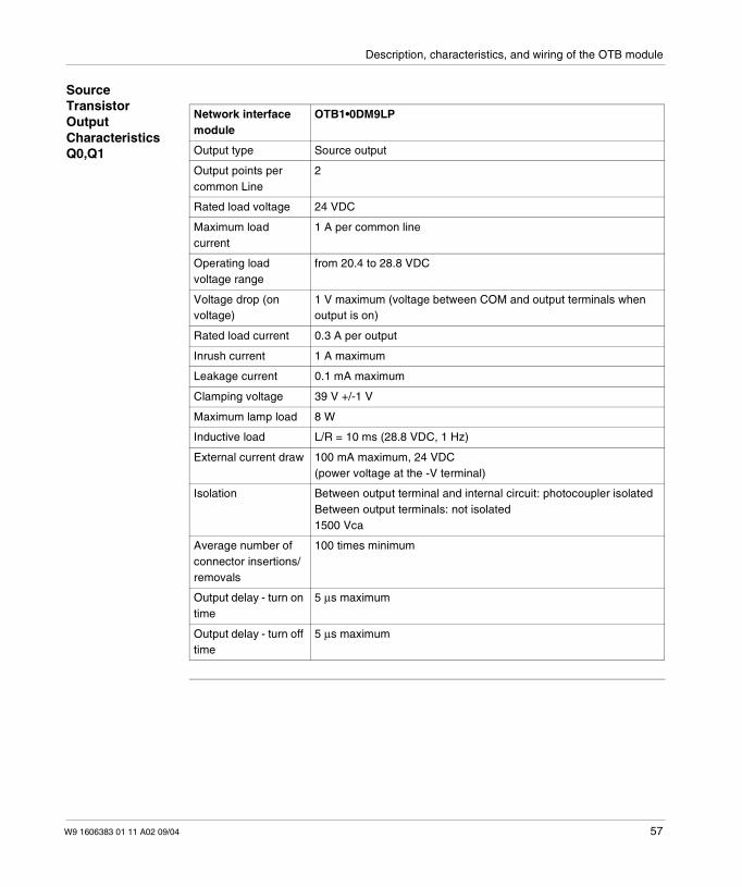
SourceTransistorOutputCharacteristicsQ0,Q1
Network interfacemodule
OTB1•0DM9LP
Output type Source output
Output points percommon Line
2
Rated load voltage 24 VDC
Maximum loadcurrent
1 A per common line
Operating loadvoltage range
from 20.4 to 28.8 VDC
Voltage drop (onvoltage)
1 V maximum (voltage between COM and output terminals whenoutput is on)
Rated load current 0.3 A per output
Inrush current 1 A maximum
Leakage current 0.1 mA maximum
Clamping voltage 39 V +/-1 V
Maximum lamp load 8 W
Inductive load L/R = 10 ms (28.8 VDC, 1 Hz)
External current draw 100 mA maximum, 24 VDC(power voltage at the -V terminal)
Isolation Between output terminal and internal circuit: photocoupler isolatedBetween output terminals: not isolated1500 Vca
Average number ofconnector insertions/removals
100 times minimum
Output delay - turn ontime
5 µs maximum
Output delay - turn offtime
5 µs maximum
W9 1606383 01 11 A02 09/04 57
Description, characteristics, and wiring of the OTB module
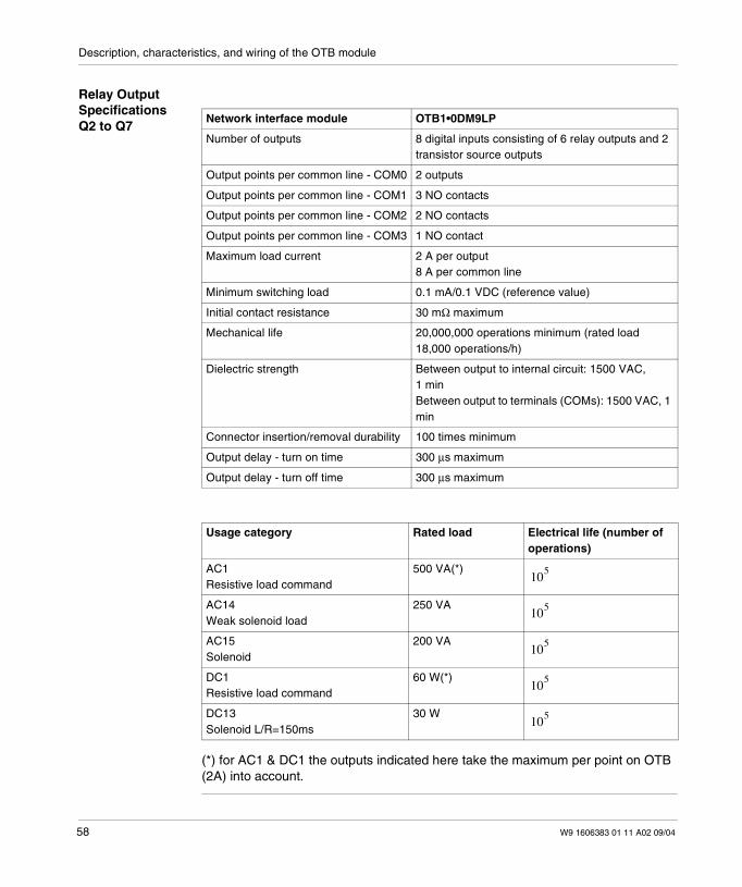
Relay OutputSpecificationsQ2 to Q7
(*) for AC1 & DC1 the outputs indicated here take the maximum per point on OTB(2A) into account.
Network interface module OTB1•0DM9LP
Number of outputs 8 digital inputs consisting of 6 relay outputs and 2transistor source outputs
Output points per common line - COM0 2 outputs
Output points per common line - COM1 3 NO contacts
Output points per common line - COM2 2 NO contacts
Output points per common line - COM3 1 NO contact
Maximum load current 2 A per output8 A per common line
Minimum switching load 0.1 mA/0.1 VDC (reference value)
Initial contact resistance 30 mΩ maximum
Mechanical life 20,000,000 operations minimum (rated load18,000 operations/h)
Dielectric strength Between output to internal circuit: 1500 VAC,1 minBetween output to terminals (COMs): 1500 VAC, 1min
Connector insertion/removal durability 100 times minimum
Output delay - turn on time 300 µs maximum
Output delay - turn off time 300 µs maximum
Usage category Rated load Electrical life (number ofoperations)
AC1Resistive load command
500 VA(*)
AC14Weak solenoid load
250 VA
AC15Solenoid
200 VA
DC1Resistive load command
60 W(*)
DC13Solenoid L/R=150ms
30 W
105
105
105
105
105
58 W9 1606383 01 11 A02 09/04
Description, characteristics, and wiring of the OTB module
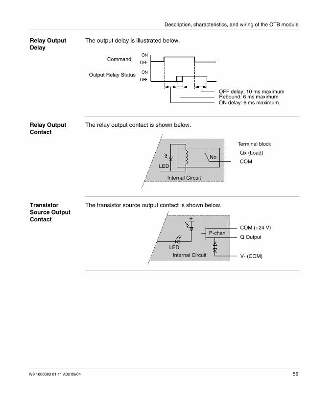
Relay OutputDelay
The output delay is illustrated below.
Relay OutputContact
The relay output contact is shown below.
TransistorSource OutputContact
The transistor source output contact is shown below.
OFF delay: 10 ms maximum
Command
Output Relay Status
Rebound: 6 ms maximumON delay: 6 ms maximum
Internal Circuit
No
LED
Qx (Load)
COM
Terminal block
P-chan
LED
Q Output
COM (+24 V)
V- (COM)Internal Circuit
W9 1606383 01 11 A02 09/04 59
Description, characteristics, and wiring of the OTB module
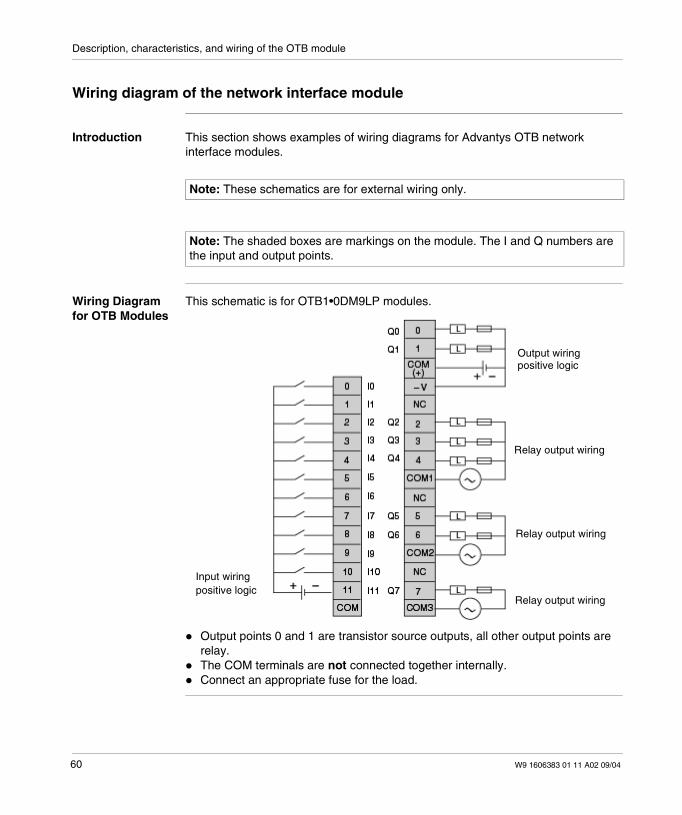
Wiring diagram of the network interface module
Introduction This section shows examples of wiring diagrams for Advantys OTB networkinterface modules.
Wiring Diagramfor OTB Modules
This schematic is for OTB1•0DM9LP modules.
Output points 0 and 1 are transistor source outputs, all other output points arerelay.The COM terminals are not connected together internally.Connect an appropriate fuse for the load.
Note: These schematics are for external wiring only.
Note: The shaded boxes are markings on the module. The I and Q numbers arethe input and output points.
Output wiring
Input wiring
Relay output wiring
Relay output wiring
Relay output wiring
positive logic
positive logic
60 W9 1606383 01 11 A02 09/04
Description, characteristics, and wiring of the OTB module
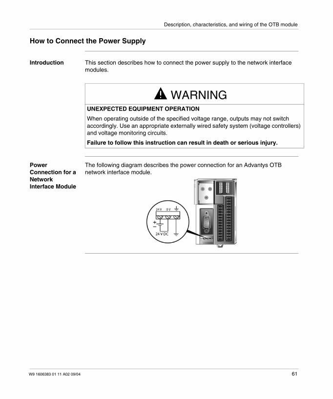
How to Connect the Power Supply
Introduction This section describes how to connect the power supply to the network interfacemodules.
PowerConnection for aNetworkInterface Module
The following diagram describes the power connection for an Advantys OTBnetwork interface module.
WARNINGUNEXPECTED EQUIPMENT OPERATION
When operating outside of the specified voltage range, outputs may not switchaccordingly. Use an appropriate externally wired safety system (voltage controllers)and voltage monitoring circuits.
Failure to follow this instruction can result in death or serious injury.
W9 1606383 01 11 A02 09/04 61
Description, characteristics, and wiring of the OTB module
NetworkInterface ModulePower SupplySpecifications
The following table describes the power supply specifications for the networkinterface module.
Item Characteristics
Power supplyvoltage
Rated power voltage: 24 VDCAllowable range: from 20.4 to 26.4 VDCNote:Momentary power interruption for 10 ms or less at 24 VDC is notrecognized as failure.
Inrush currentflow at power-up
50 A maximum
Power supplywiring
0.64 mm2 (UL1015 AWG22) or 1.02 mm2 (UL1007 AWG18)Make the power supply wiring as short as possible.
Ground wiring 0.64 mm2 (UL1015 AWG22) or 1.02 mm2 (UL1007 AWG18)Do not connect ground wire in common with ground wire of motorequipment.The earth connection should be as short as possible < 10 cm (3.9 inch).
62 W9 1606383 01 11 A02 09/04
Description, characteristics, and wiring of the OTB module
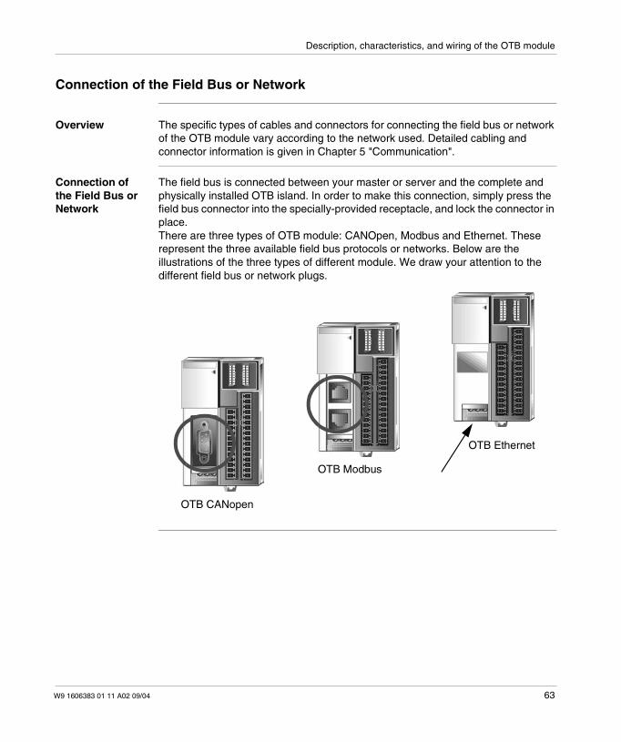
Connection of the Field Bus or Network
Overview The specific types of cables and connectors for connecting the field bus or networkof the OTB module vary according to the network used. Detailed cabling andconnector information is given in Chapter 5 "Communication".
Connection ofthe Field Bus orNetwork
The field bus is connected between your master or server and the complete andphysically installed OTB island. In order to make this connection, simply press thefield bus connector into the specially-provided receptacle, and lock the connector inplace.There are three types of OTB module: CANOpen, Modbus and Ethernet. Theserepresent the three available field bus protocols or networks. Below are theillustrations of the three types of different module. We draw your attention to thedifferent field bus or network plugs.
OTB CANopen
OTB Ethernet
OTB Modbus
W9 1606383 01 11 A02 09/04 63

Description, characteristics, and wiring of the OTB module
64 W9 1606383 01 11 A02 09/04

W9 1606383 01 11 A02 09/04
4
Description, characteristics, andwiring of the expansion modulesAt a Glance
Introduction This chapter provides an overview of the analog and Discrete I/O expansionmodules. Information on functions and wiring is given for each expansion module.
What's in thisChapter?
This chapter contains the following topics:
Topic Page
Overview of Digital I/O Modules 66
Parts Description of Digital I/O Modules 70
Specifications for the Digital I/O Modules 72
Digital I/O Module Wiring Schematics 83
Overview of Analog I/O Modules 93
Parts Description of Analog I/O Modules 94
General Specifications for the Analog I/O Modules 95
Specifications for the Analog I/O Modules 96
Analog I/O Modules Wiring Schematics 100
Communication expansion module block Wiring Schematics 103
65

Description, characteristics, and wiring of the expansion modules
Overview of Digital I/O Modules
Introduction The following section provides an overview of the digital I/O modules.
66 W9 1606383 01 11 A02 09/04

Description, characteristics, and wiring of the expansion modules
Illustrations The following illustrations are the digital input, output, and mixed I/O modules.
Module type Illustration
There are 5 digital input modules:8-point module with a terminal block(TWDDDI8DT, TWDDAI8DT)16-point module with a terminal block(TWDDDI16DT)16-point module with a connector(TWDDDI16DK)32-point module with a connector(TWDDDI32DK)
These modules can be attached to anycommunication module.
TWDDDI8DT
TWDDDI16DT TWDDDI32DK
TWDDDI16DKTWDDAI8DT
W9 1606383 01 11 A02 09/04 67
Description, characteristics, and wiring of the expansion modules
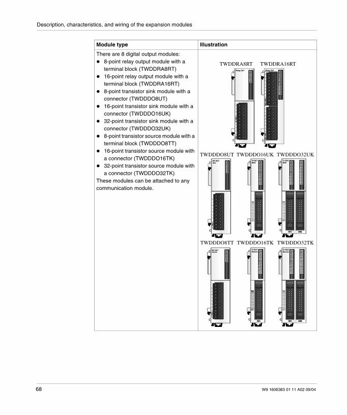
There are 8 digital output modules:8-point relay output module with aterminal block (TWDDRA8RT)16-point relay output module with aterminal block (TWDDRA16RT)8-point transistor sink module with aconnector (TWDDDO8UT)16-point transistor sink module with aconnector (TWDDDO16UK)32-point transistor sink module with aconnector (TWDDDO32UK)8-point transistor source module with aterminal block (TWDDDO8TT)16-point transistor source module witha connector (TWDDDO16TK)32-point transistor source module witha connector (TWDDDO32TK)
These modules can be attached to anycommunication module.
Module type Illustration
TWDDRA8RT TWDDRA16RT
TWDDDO8UT TWDDDO16UK TWDDDO32UK
TWDDDO8TT TWDDDO16TK TWDDDO32TK
68 W9 1606383 01 11 A02 09/04

Description, characteristics, and wiring of the expansion modules
There are 2 digital mixed input and outputmodules:
4-point input/4-point output modulewith a terminal block (TWDDMM8RT)16-point input/8-point output modulewith a wire-clamp terminal block(TWDDMM24DRF)
These modules can be attached to anycommunication module.
Module type Illustration
TWDDMM8RT TWDDMM24DRF
W9 1606383 01 11 A02 09/04 69
Description, characteristics, and wiring of the expansion modules
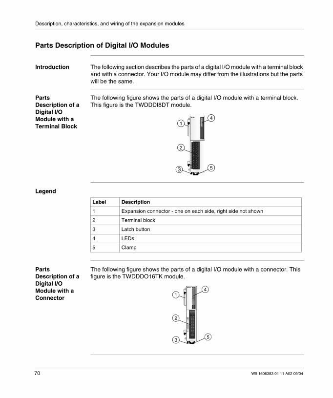
Parts Description of Digital I/O Modules
Introduction The following section describes the parts of a digital I/O module with a terminal blockand with a connector. Your I/O module may differ from the illustrations but the partswill be the same.
PartsDescription of aDigital I/OModule with aTerminal Block
The following figure shows the parts of a digital I/O module with a terminal block.This figure is the TWDDDI8DT module.
Legend
PartsDescription of aDigital I/OModule with aConnector
The following figure shows the parts of a digital I/O module with a connector. Thisfigure is the TWDDDO16TK module.
2
14
53
Label Description
1 Expansion connector - one on each side, right side not shown
2 Terminal block
3 Latch button
4 LEDs
5 Clamp
2
4
53
1
70 W9 1606383 01 11 A02 09/04

Description, characteristics, and wiring of the expansion modules
Legend
Label Description
1 Expansion connector - one on each side, right side not shown
2 Connector
3 Latch button
4 LEDs
5 Clamp
W9 1606383 01 11 A02 09/04 71
Description, characteristics, and wiring of the expansion modules
Specifications for the Digital I/O Modules
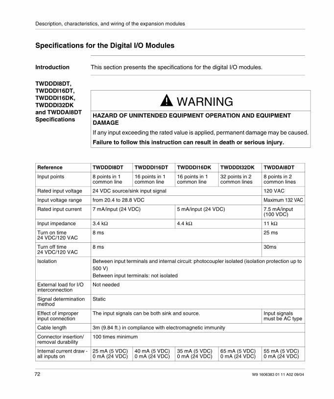
Introduction This section presents the specifications for the digital I/O modules.
TWDDDI8DT,TWDDDI16DT,TWDDDI16DK,TWDDDI32DKand TWDDAI8DTSpecifications
WARNINGHAZARD OF UNINTENDED EQUIPMENT OPERATION AND EQUIPMENTDAMAGE
If any input exceeding the rated value is applied, permanent damage may be caused.
Failure to follow this instruction can result in death or serious injury.
Reference TWDDDI8DT TWDDDI16DT TWDDDI16DK TWDDDI32DK TWDDAI8DT
Input points 8 points in 1common line
16 points in 1common line
16 points in 1common line
32 points in 2common lines
8 points in 2common lines
Rated input voltage 24 VDC source/sink input signal 120 VAC
Input voltage range from 20.4 to 28.8 VDC Maximum 132 VAC
Rated input current 7 mA/input (24 VDC) 5 mA/input (24 VDC) 7.5 mA/input(100 VDC)
Input impedance 3.4 kΩ 4.4 kΩ 11 kΩ
Turn on time24 VDC/120 VAC
8 ms 25 ms
Turn off time24 VDC/120 VAC
8 ms 30ms
Isolation Between input terminals and internal circuit: photocoupler isolated (isolation protection up to500 V)Between input terminals: not isolated
External load for I/Ointerconnection
Not needed
Signal determinationmethod
Static
Effect of improperinput connection
The input signals can be both sink and source. Input signalsmust be AC type
Cable length 3m (9.84 ft.) in compliance with electromagnetic immunity
Connector insertion/removal durability
100 times minimum
Internal current draw -all inputs on
25 mA (5 VDC)0 mA (24 VDC)
40 mA (5 VDC)0 mA (24 VDC)
35 mA (5 VDC)0 mA (24 VDC)
65 mA (5 VDC)0 mA (24 VDC)
55 mA (5 VDC)0 mA (24 VDC)
72 W9 1606383 01 11 A02 09/04
Description, characteristics, and wiring of the expansion modules
TWDDDI8DT,TWDDDI16DT,TWDDDI16DK,TWDDDI32DKand TWDDAI8DTOperating Range
The operating range of the Type 1 (IEC 61131-2) input module is shown below.
Internal current draw -all inputs off
5 mA (5 VDC)0 mA (24 VDC)
5 mA (5 VDC)0 mA (24 VDC)
5 mA (5 VDC)0 mA (24 VDC)
10 mA (5 VDC)0 mA (24 VDC)
25 mA (5 VDC)0 mA (24 VDC)
Weight 85 g (3 oz) 100 g (3.5 oz) 65 g (2.3 oz) 100 g (3.5 oz) 81 g (2.9 oz)
Reference TWDDDI8DT TWDDDI16DT TWDDDI16DK TWDDDI32DK TWDDAI8DT
ON Area
Transition
OFF Area
Input Current (mA)
Inpu
tVol
tage
(VD
C)
Area
ON Area
Transition
OFF Area
Input Current (mA)
Inpu
tVol
tage
(VD
C)
Area
TWDDDI8DT and TWDDDI16DT TWDDDI16DK and TWDDDI32DK
TWDDAI8DT
Inpu
tVol
tage
(VA
C)
Input Current (mA)
ON Area
Transition
OFF Area
Area
W9 1606383 01 11 A02 09/04 73
Description, characteristics, and wiring of the expansion modules
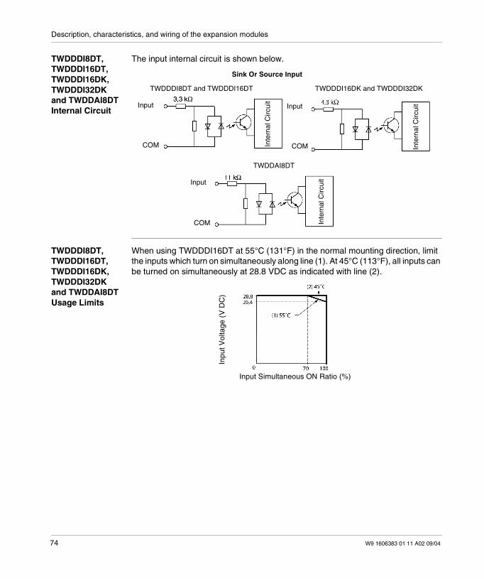
TWDDDI8DT,TWDDDI16DT,TWDDDI16DK,TWDDDI32DKand TWDDAI8DTInternal Circuit
The input internal circuit is shown below.
TWDDDI8DT,TWDDDI16DT,TWDDDI16DK,TWDDDI32DKand TWDDAI8DTUsage Limits
When using TWDDDI16DT at 55°C (131°F) in the normal mounting direction, limitthe inputs which turn on simultaneously along line (1). At 45°C (113°F), all inputs canbe turned on simultaneously at 28.8 VDC as indicated with line (2).
Inte
rnal
Circ
uitInput
COM
TWDDDI8DT and TWDDDI16DT TWDDDI16DK and TWDDDI32DK
Inte
rnal
Circ
uit
Input
COM
Sink Or Source Input
Inte
rnal
Circ
uitInput
COM
TWDDAI8DT
Input Simultaneous ON Ratio (%)
Inpu
tVol
tage
(VD
C)
74 W9 1606383 01 11 A02 09/04

Description, characteristics, and wiring of the expansion modules
When using TWDDDI16DK and TWDDDI32DK at 55°C (131°F), limit the inputswhich turn on simultaneously on each connector along line (3). This limitationapplies per connecter. At 30°C (86°F), all inputs can be turned on simultaneously at28.8 VDC as indicated with line (4).
When using TWDDDI8DT, all inputs can be turned on simultaneously at 55°C(131°F), input voltage 28.8 VDC.
Input Simultaneous ON Ratio (%)
Inpu
tVol
tage
(VD
C)
W9 1606383 01 11 A02 09/04 75
Description, characteristics, and wiring of the expansion modules
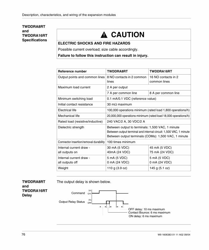
TWDDRA8RTandTWDDRA16RTSpecifications
TWDDRA8RTandTWDDRA16RTDelay
The output delay is shown below.
CAUTIONELECTRIC SHOCKS AND FIRE HAZARDS
Possible current overload; size cable accordingly.
Failure to follow this instruction can result in injury.
Reference number TWDDRA8RT TWDDRA16RT
Output points and common lines 8 NO contacts in 2 commonlines
16 NO contacts in 2common lines
Maximum load current 2 A per output
7 A per common line 8 A per common line
Minimum switching load 0.1 mA/0.1 VDC (reference value)
Initial contact resistance 30 mΩ maximum
Electrical life 100,000 operations minimum (rated load 1,800 operations/h)
Mechanical life 20,000,000 operations minimum (rated load 18,000 operations/h)
Rated load (resistive/inductive) 240 VAC/2 A, 30 VDC/2 A
Dielectric strength Between output to terminals: 1,500 VAC, 1 minuteBetween output terminal and internal circuit: 1,500 VAC, 1 minuteBetween output terminals (COMs): 1,500 VAC, 1 minute
Connector insertion/removal durability 100 times minimum
Internal current draw -all outputs on
30 mA (5 VDC)40mA (24 VDC)
45 mA (5 VDC)75 mA (24 VDC)
Internal current draw -all outputs off
5 mA (5 VDC)0 mA (24 VDC)
5 mA (5 VDC)0 mA (24 VDC)
Weight 110 g (3.9 oz) 145 g (5.1 oz)
OFF delay: 10 ms maximum
Command
Output Relay Status
Contact Bounce: 6 ms maximumON delay: 6 ms maximum
76 W9 1606383 01 11 A02 09/04
Description, characteristics, and wiring of the expansion modules
TWDDDO8UT,TWDDDO16UK,andTWDDDO32UKSpecifications
Reference number TWDDDO8UT TWDDDO16UK TWDDDO32UK
Output type Transistor sink output
Output points per common Line 8 points in 1common line
16 points in 1common line
32 points in 2common lines
Rated load voltage 24 VDC
Operating load voltage range from 20.4 to 28.8 VDC
Rated load current 0.3 A per output 0.1 A per output
Maximum load current 0.36 A per output3 A per commonline
0.12 A per output1 A per common line
Voltage drop (on voltage) 1 V maximum (voltage between COM and outputterminals when output is on)
Inrush current 1 A maximum
Leakage current 0.1 A maximum
Clamping voltage 39 V +/-1 V
Maximum lamp load 8 W
Inductive load L/R = 10 ms (28.8 VDC, 1 Hz)
External current draw 100 mA maximum, 24 VDC(power voltage at the +V terminal)
Isolation Between input terminals and internal circuit: photocouplerisolated (isolation protection up to 500 V)Between input terminals: not isolated
Connector insertion/removaldurability
100 times minimum
Internal current draw -all outputs on
10 mA (5 VDC)20 mA (24 VDC)
10 mA (5 VDC)40mA (24 VDC)
20 mA (5 VDC)70 mA (24 VDC)
Internal current draw -all outputs off
5 mA (5 VDC)0 mA (24 VDC)
5 mA (5 VDC)0 mA (24 VDC)
10 mA (5 VDC)0 mA (24 VDC)
Output delay Turn on time: 300 µs maximumTurn off time: 300 µs maximum
Weight 85 g (3 oz) 70 g (2.5 oz) 105 g (3.7 oz)
W9 1606383 01 11 A02 09/04 77
Description, characteristics, and wiring of the expansion modules
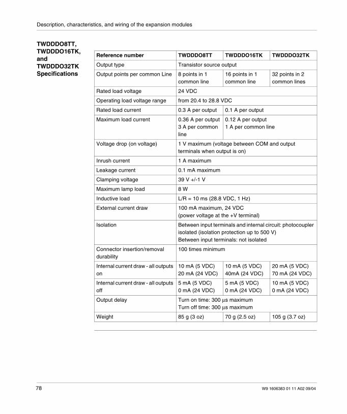
TWDDDO8TT,TWDDDO16TK,andTWDDDO32TKSpecifications
Reference number TWDDDO8TT TWDDDO16TK TWDDDO32TK
Output type Transistor source output
Output points per common Line 8 points in 1common line
16 points in 1common line
32 points in 2common lines
Rated load voltage 24 VDC
Operating load voltage range from 20.4 to 28.8 VDC
Rated load current 0.3 A per output 0.1 A per output
Maximum load current 0.36 A per output3 A per commonline
0.12 A per output1 A per common line
Voltage drop (on voltage) 1 V maximum (voltage between COM and outputterminals when output is on)
Inrush current 1 A maximum
Leakage current 0.1 mA maximum
Clamping voltage 39 V +/-1 V
Maximum lamp load 8 W
Inductive load L/R = 10 ms (28.8 VDC, 1 Hz)
External current draw 100 mA maximum, 24 VDC(power voltage at the +V terminal)
Isolation Between input terminals and internal circuit: photocouplerisolated (isolation protection up to 500 V)Between input terminals: not isolated
Connector insertion/removaldurability
100 times minimum
Internal current draw - all outputson
10 mA (5 VDC)20 mA (24 VDC)
10 mA (5 VDC)40mA (24 VDC)
20 mA (5 VDC)70 mA (24 VDC)
Internal current draw - all outputsoff
5 mA (5 VDC)0 mA (24 VDC)
5 mA (5 VDC)0 mA (24 VDC)
10 mA (5 VDC)0 mA (24 VDC)
Output delay Turn on time: 300 µs maximumTurn off time: 300 µs maximum
Weight 85 g (3 oz) 70 g (2.5 oz) 105 g (3.7 oz)
78 W9 1606383 01 11 A02 09/04

Description, characteristics, and wiring of the expansion modules
TWDDMM8DRTandTWDDMM24DRFInputSpecifications
WARNINGHAZARD OF UNINTENDED EQUIPMENT OPERATION AND EQUIPMENTDAMAGE
If any input exceeding the rated value is applied, permanent damage may be caused.
Failure to follow this instruction can result in death or serious injury.
Reference number TWDDMM8DRT TWDDMM24DRF
I/O points 4 inputs and 4 outputs 16 inputs and 8 outputs
Rated input voltage 24 VDC source/sink input signal
Input voltage range from 20.4 to 28.8 VDC
Rated input current 7 mA/input (24 VDC)
Input impedance 3.4 kΩ
Turn on time (24 VDC) 4 ms (24 VDC)
Turn off time (24 VDC) 4 ms (24 VDC)
Isolation Between input terminals and internal circuit: photocouplerisolated (isolation protection up to 500 V)Between input terminals: not isolated
External load for I/Ointerconnection
Not needed
Signal determination method Static
Effect of improper inputconnection
Both sinking and sourcing input signals can be connected.
Cable length 3m (9.84 ft.) in compliance with electromagnetic immunity
Connector insertion/removaldurability
100 times minimum Not removable
Internal current draw -all I/O on
25 mA (5 VDC)20 mA (24 VDC)
65 mA (5 VDC)45 mA (24 VDC)
Internal current draw - all I/O off 5 mA (5 VDC)0 mA (24 VDC)
10 mA (5 VDC)0 mA (24 VDC)
Weight 95 g (3.3 oz) 140 g (4.9 oz)
W9 1606383 01 11 A02 09/04 79
Description, characteristics, and wiring of the expansion modules
TWDDMM8DRTandTWDDMM24DRFInput OperatingRange
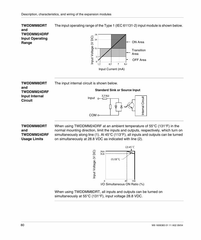
The input operating range of the Type 1 (IEC 61131-2) input module is shown below.
TWDDMM8DRTandTWDDMM24DRFInput InternalCircuit
The input internal circuit is shown below.
TWDDMM8DRTandTWDDMM24DRFUsage Limits
When using TWDDMM24DRF at an ambient temperature of 55°C (131°F) in thenormal mounting direction, limit the inputs and outputs, respectively, which turn onsimultaneously along line (1). At 45°C (113°F), all inputs and outputs can be turnedon simultaneously at 28.8 VDC as indicated with line (2).
When using TWDDMM8DRT, all inputs and outputs can be turned onsimultaneously at 55°C (131°F), input voltage 28.8 VDC.
ON Area
Transition
OFF Area
Input Current (mA)
Inpu
tVol
tage
(VD
C)
Area
Input
COM
Standard Sink or Source Input
Inte
rnal
Circ
uit
I/O Simultaneous ON Ratio (%)
Inpu
tVol
tage
(VD
C)
80 W9 1606383 01 11 A02 09/04
Description, characteristics, and wiring of the expansion modules
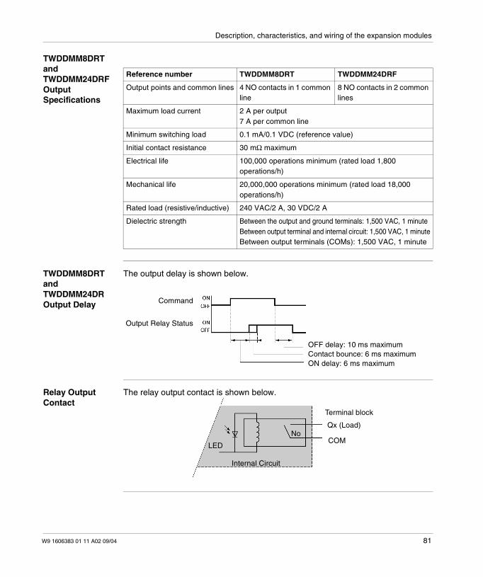
TWDDMM8DRTandTWDDMM24DRFOutputSpecifications
TWDDMM8DRTandTWDDMM24DROutput Delay
The output delay is shown below.
Relay OutputContact
The relay output contact is shown below.
Reference number TWDDMM8DRT TWDDMM24DRF
Output points and common lines 4 NO contacts in 1 commonline
8 NO contacts in 2 commonlines
Maximum load current 2 A per output7 A per common line
Minimum switching load 0.1 mA/0.1 VDC (reference value)
Initial contact resistance 30 mΩ maximum
Electrical life 100,000 operations minimum (rated load 1,800operations/h)
Mechanical life 20,000,000 operations minimum (rated load 18,000operations/h)
Rated load (resistive/inductive) 240 VAC/2 A, 30 VDC/2 A
Dielectric strength Between the output and ground terminals: 1,500 VAC, 1 minuteBetween output terminal and internal circuit: 1,500 VAC, 1 minuteBetween output terminals (COMs): 1,500 VAC, 1 minute
OFF delay: 10 ms maximum
Command
Output Relay Status
Contact bounce: 6 ms maximumON delay: 6 ms maximum
Internal Circuit
LED
Qx (Load)
COM
Terminal block
No
W9 1606383 01 11 A02 09/04 81
Description, characteristics, and wiring of the expansion modules
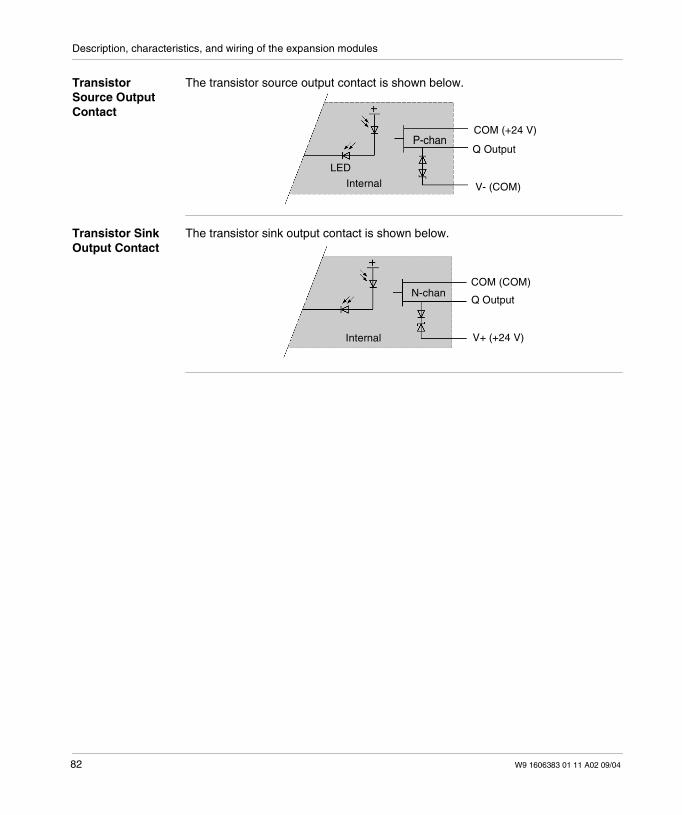
TransistorSource OutputContact
The transistor source output contact is shown below.
Transistor SinkOutput Contact
The transistor sink output contact is shown below.
P-chan
LED
Q Output
COM (+24 V)
V- (COM)Internal
Internal
Q Output
COM (COM)
V+ (+24 V)
N-chan
82 W9 1606383 01 11 A02 09/04
Description, characteristics, and wiring of the expansion modules
Digital I/O Module Wiring Schematics
Introduction This section shows examples of wiring schematics for the digital I/O modules.
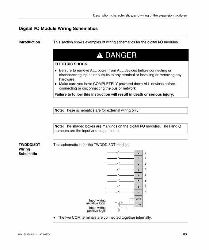
TWDDDI8DTWiringSchematic
This schematic is for the TWDDDI8DT module.
The two COM terminals are connected together internally.
DANGERELECTRIC SHOCK
Be sure to remove ALL power from ALL devices before connecting ordisconnecting inputs or outputs to any terminal or installing or removing anyhardware.Make sure you have COMPLETELY powered down ALL devices beforeconnecting or disconnecting the bus or network.
Failure to follow this instruction will result in death or serious injury.
Note: These schematics are for external wiring only.
Note: The shaded boxes are markings on the digital I/O modules. The I and Qnumbers are the input and output points.
Input wiring
Input wiringnegative logic
positive logic
W9 1606383 01 11 A02 09/04 83
Description, characteristics, and wiring of the expansion modules
TWDDDI16DTWiringSchematic
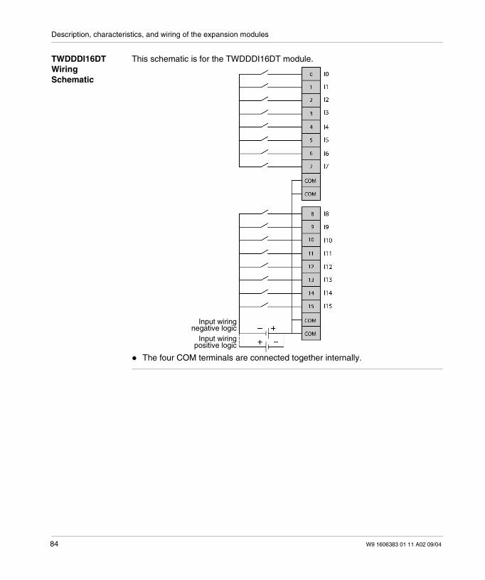
This schematic is for the TWDDDI16DT module.
The four COM terminals are connected together internally.
Input wiring
Input wiringnegative logic
positive logic
84 W9 1606383 01 11 A02 09/04
Description, characteristics, and wiring of the expansion modules
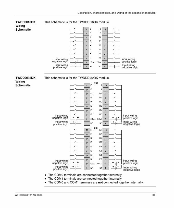
TWDDDI16DKWiringSchematic
This schematic is for the TWDDDI16DK module.
TWDDDI32DKWiringSchematic
This schematic is for the TWDDDI32DK module.
The COM0 terminals are connected together internally.The COM1 terminals are connected together internally.The COM0 and COM1 terminals are not connected together internally.
Input wiring
Input wiringnegative logic
positive logicInput wiring
Input wiringpositive logic
negative logic
Input wiring
Input wiringnegative logic
positive logicInput wiring
Input wiringpositive logic
negative logic
Input wiring
Input wiringpositive logic
negative logic
Input wiring
Input wiringnegative logic
positive logic
W9 1606383 01 11 A02 09/04 85
Description, characteristics, and wiring of the expansion modules
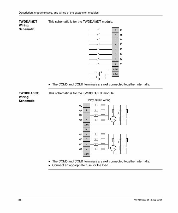
TWDDAI8DTWiringSchematic
This schematic is for the TWDDAI8DT module.
The COM0 and COM1 terminals are not connected together internally.
TWDDRA8RTWiringSchematic
This schematic is for the TWDDRA8RT module.
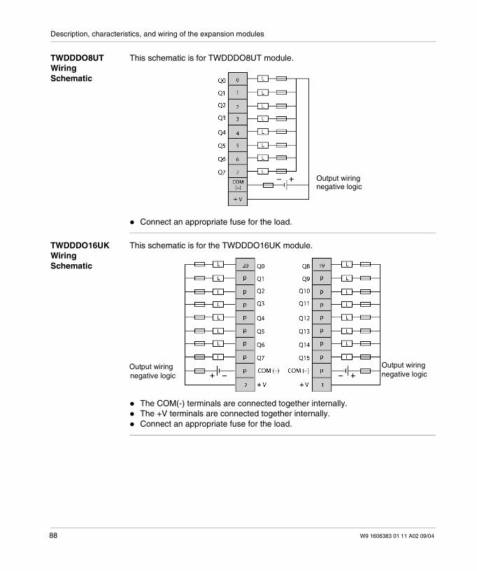
The COM0 and COM1 terminals are not connected together internally.Connect an appropriate fuse for the load.
Relay output wiring
86 W9 1606383 01 11 A02 09/04
Description, characteristics, and wiring of the expansion modules
TWDDRA16RTWiringSchematic
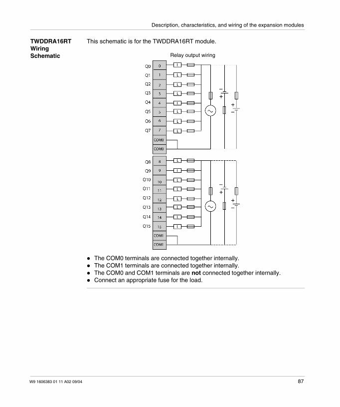
This schematic is for the TWDDRA16RT module.
The COM0 terminals are connected together internally.The COM1 terminals are connected together internally.The COM0 and COM1 terminals are not connected together internally.Connect an appropriate fuse for the load.
Relay output wiring
W9 1606383 01 11 A02 09/04 87
Description, characteristics, and wiring of the expansion modules
TWDDDO8UTWiringSchematic
This schematic is for TWDDDO8UT module.
Connect an appropriate fuse for the load.
TWDDDO16UKWiringSchematic
This schematic is for the TWDDDO16UK module.
The COM(-) terminals are connected together internally.The +V terminals are connected together internally.Connect an appropriate fuse for the load.
Output wiringnegative logic
Output wiring Output wiringnegative logic negative logic
88 W9 1606383 01 11 A02 09/04
Description, characteristics, and wiring of the expansion modules
TWDDDO32UKWiringSchematic
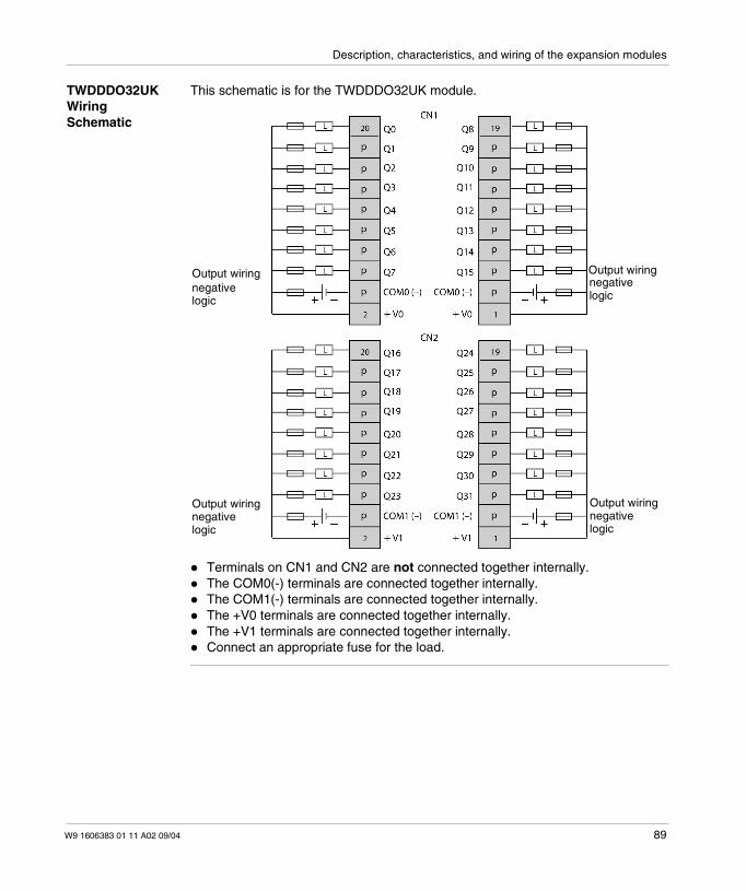
This schematic is for the TWDDDO32UK module.
Terminals on CN1 and CN2 are not connected together internally.The COM0(-) terminals are connected together internally.The COM1(-) terminals are connected together internally.The +V0 terminals are connected together internally.The +V1 terminals are connected together internally.Connect an appropriate fuse for the load.
Output wiring Output wiring
Output wiring Output wiring
negative
negative
negative
negative
logic logic
logiclogic
W9 1606383 01 11 A02 09/04 89
Description, characteristics, and wiring of the expansion modules
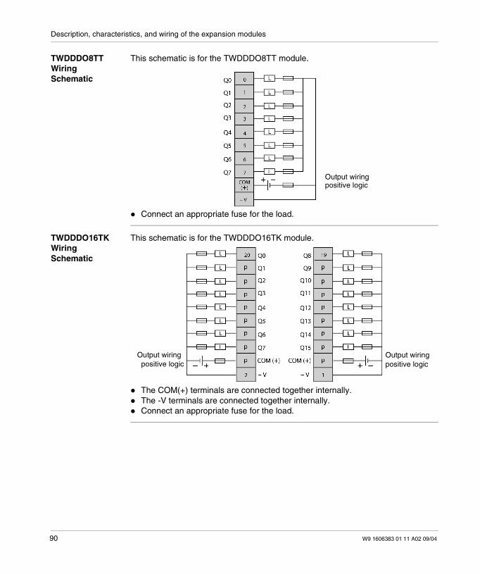
TWDDDO8TTWiringSchematic
This schematic is for the TWDDDO8TT module.
Connect an appropriate fuse for the load.
TWDDDO16TKWiringSchematic
This schematic is for the TWDDDO16TK module.
The COM(+) terminals are connected together internally.The -V terminals are connected together internally.Connect an appropriate fuse for the load.
Output wiringpositive logic
Output wiringOutput wiringpositive logic positive logic
90 W9 1606383 01 11 A02 09/04

Description, characteristics, and wiring of the expansion modules
TWDDDO32TKWiringSchematic
This schematic is for the TWDDDO32TK module.
Terminals CN1 and CN2 are not connected together internally.The COM0(+) terminals are connected together internally.The COM1(+) terminals are connected together internally.The -V0 terminals are connected together internally.The -V1 terminals are connected together internally.Connect an appropriate fuse for the load.
Output wiringOutput wiringpositive logic
Output wiring
positive logic
positive logic
Output wiringpositive logic
W9 1606383 01 11 A02 09/04 91
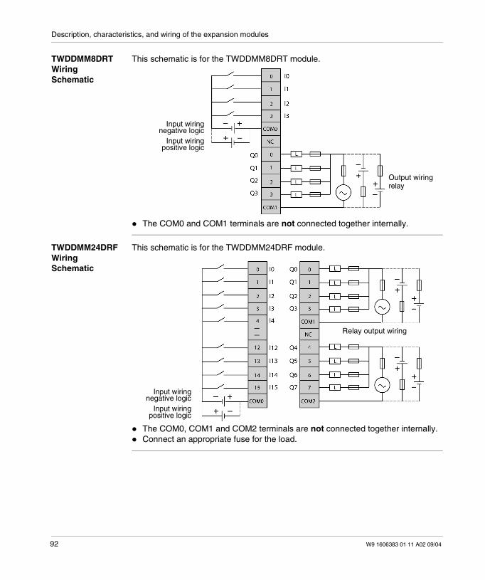
Description, characteristics, and wiring of the expansion modules
TWDDMM8DRTWiringSchematic
This schematic is for the TWDDMM8DRT module.
The COM0 and COM1 terminals are not connected together internally.
TWDDMM24DRFWiringSchematic
This schematic is for the TWDDMM24DRF module.
The COM0, COM1 and COM2 terminals are not connected together internally.Connect an appropriate fuse for the load.
Output wiring
Input wiring
Input wiringnegative logic
positive logic
relay
Relay output wiring
Input wiring
Input wiringnegative logic
positive logic
92 W9 1606383 01 11 A02 09/04
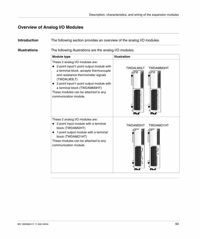
Description, characteristics, and wiring of the expansion modules
Overview of Analog I/O Modules
Introduction The following section provides an overview of the analog I/O modules.
Illustrations The following illustrations are the analog I/O modules.
Module type Illustration
These 2 analog I/O modules are:2-point input/1-point output module witha terminal block, accepts thermocoupleand resistance thermometer signals(TWDALM3LT)2-point input/1-point output module witha terminal block (TWDAMM3HT)
These modules can be attached to anycommunication module.
These 2 analog I/O modules are:2-point input module with a terminalblock (TWDAMI2HT)1-point output module with a terminalblock (TWDAMO1HT)
These modules can be attached to anycommunication module.
TWDALM3LT TWDAMM3HT
TWDAMI2HT TWDAMO1HT
W9 1606383 01 11 A02 09/04 93
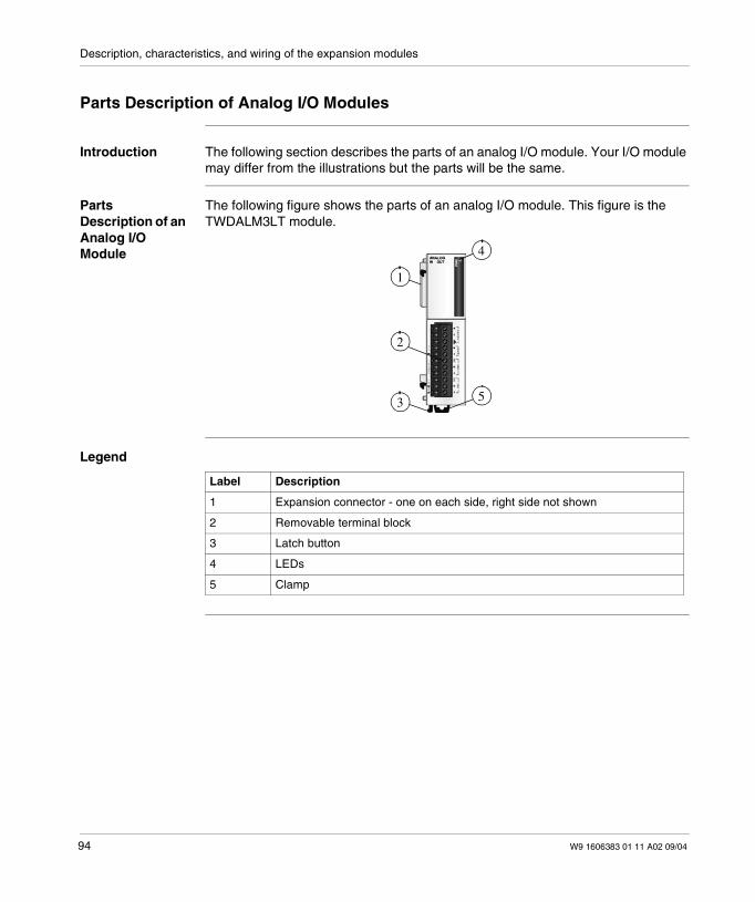
Description, characteristics, and wiring of the expansion modules
Parts Description of Analog I/O Modules
Introduction The following section describes the parts of an analog I/O module. Your I/O modulemay differ from the illustrations but the parts will be the same.
PartsDescription of anAnalog I/OModule
The following figure shows the parts of an analog I/O module. This figure is theTWDALM3LT module.
Legend
2
1
4
53
Label Description
1 Expansion connector - one on each side, right side not shown
2 Removable terminal block
3 Latch button
4 LEDs
5 Clamp
94 W9 1606383 01 11 A02 09/04

Description, characteristics, and wiring of the expansion modules
General Specifications for the Analog I/O Modules
Introduction This section is general specifications for analog I/O modules.
GeneralSpecifications
Reference TWDALM3LT TWDAMM3HT TWDAMI2HT TWDAMO1HT
Rated power voltage 24 VDC
Allowable voltagerange
from 20.4 to 28.8 VDC
Average number ofconnector insertions/removals
100 times minimum
Internal current draw -internal power
50mA (5 VDC)0 mA (24 VDC)
Internal current draw -external power
40mA (24 VDC)
Weight 85 g (3oz)
W9 1606383 01 11 A02 09/04 95
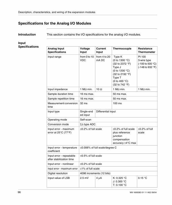
Description, characteristics, and wiring of the expansion modules
Specifications for the Analog I/O Modules
Introduction This section contains the I/O specifications for the analog I/O modules.
InputSpecifications
Analog InputSpecifications
VoltageInput
CurrentInput
Thermocouple ResistanceThermometer
Input range from 0 to 10VDC
from 4 to 20mA DC
Type K(0 to 1300 °C)(32 to 2372 °F)Type J(0 to 1200 °C)(32 to 2192 °F)Type T(0 to 400 °C)(32 to 742 °F)
Pt 1003-wire type(-100 to 500 °C)(-148 to 932 °F)
Input impedance 1 MΩ min. 10 Ω 1 MΩ min. 1 MΩ min.
Sample duration time 16 ms max. 50 ms max.
Sample repetition time 16 ms max. 50 ms max.
Measurement conversiontime
32 ms 100 ms
Input type Single-ended input
Differential input
Operating mode Self-scan
Conversion mode Σ∆ type ADC
Input error - maximumerror at 25°C (77°F)
±0.2% of full scale ±0.2% of full scaleplus referencejunctioncompensationaccuracy ±4°C max
±0.2% of fullscale
Input error - temperaturecoefficient
±0.006% of full scale/degree C
Input error - repeatableafter stabilization time
±0.5% of full scale
Input error - nonlinear ±0.2% of full scale
Input error - maximum error ±1% of full scale
Digital resolution 4096 increments (12 bits)
Input value of LSB 2.5 mV 4 µA K: 0.325 °CJ: 0.300 °CT: 0.100 °C
0.15 °C
96 W9 1606383 01 11 A02 09/04
Description, characteristics, and wiring of the expansion modules
Data type in applicationprogram
0 to 4095 (12 bit data)
-32768 to 32767 (optional range designation)2
Monotonicity Yes
Input data out of range Detectable3
Noise resistance - maximumtemporary deviation duringelectrical noise tests
±3% maximum when a 500 V clamp voltage isapplied to the power and I/O wiring
Accuracy is notassured whennoise is applied
Noise resistance -common modecharacteristics
Common mode reject ration (CMRR): -50 dB
Noise resistance -common mode voltage
16 VDC
Noise resistance -input filter
No
Noise resistance - cable Twisted-pair shieldedcable is recommended forimproved noise immunity
—
Noise resistance - crosstalk 2 LSB maximum
Dielectric strength 500 V between input and power circuit
Type of protection Photocoupler between input and internal circuit
Maximum permanent allowedoverload (no damage)
13 VDC 40 mA DC —
Selection of analog inputsignal type
Using software programming
Calibration or verificationto maintain rated accuracy
Approximately 10 years
Note:1. Total input system transfer time = repetition of the sample x 22. The 12-bit data (0 to 4095) processed in the Analog I/O module can be linear-converted
to a value between -32768 and 32767. The optional range designation and analog I/Odata minimum and maximum values can be selected using data registers allocated toanalog I/O modules.
3. When an error is detected, a corresponding error code is stored to a data registerallocated to analog I/O operating status.
Analog InputSpecifications
VoltageInput
CurrentInput
Thermocouple ResistanceThermometer
W9 1606383 01 11 A02 09/04 97
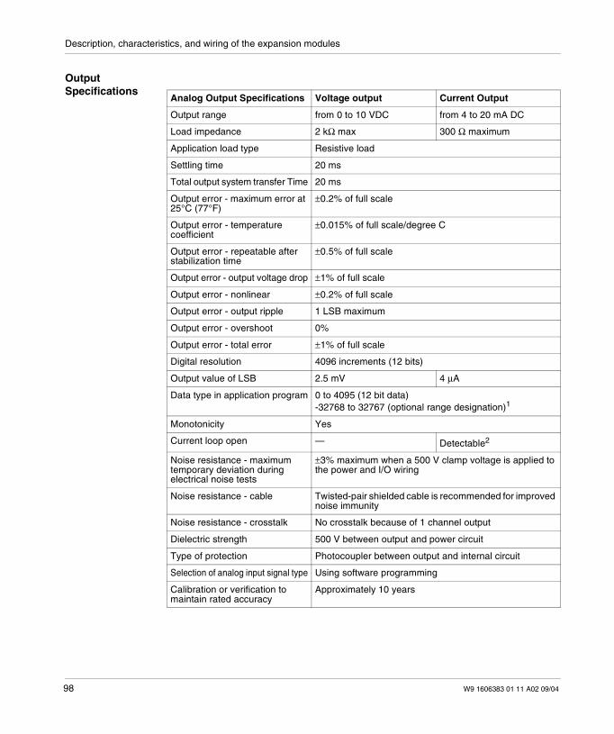
Description, characteristics, and wiring of the expansion modules
OutputSpecifications
Analog Output Specifications Voltage output Current Output
Output range from 0 to 10 VDC from 4 to 20 mA DC
Load impedance 2 kΩ max 300 Ω maximum
Application load type Resistive load
Settling time 20 ms
Total output system transfer Time 20 ms
Output error - maximum error at25°C (77°F)
±0.2% of full scale
Output error - temperaturecoefficient
±0.015% of full scale/degree C
Output error - repeatable afterstabilization time
±0.5% of full scale
Output error - output voltage drop ±1% of full scale
Output error - nonlinear ±0.2% of full scale
Output error - output ripple 1 LSB maximum
Output error - overshoot 0%
Output error - total error ±1% of full scale
Digital resolution 4096 increments (12 bits)
Output value of LSB 2.5 mV 4 µA
Data type in application program 0 to 4095 (12 bit data)-32768 to 32767 (optional range designation)1
Monotonicity Yes
Current loop open — Detectable2
Noise resistance - maximumtemporary deviation duringelectrical noise tests
±3% maximum when a 500 V clamp voltage is applied tothe power and I/O wiring
Noise resistance - cable Twisted-pair shielded cable is recommended for improvednoise immunity
Noise resistance - crosstalk No crosstalk because of 1 channel output
Dielectric strength 500 V between output and power circuit
Type of protection Photocoupler between output and internal circuit
Selection of analog input signal type Using software programming
Calibration or verification tomaintain rated accuracy
Approximately 10 years
98 W9 1606383 01 11 A02 09/04

Description, characteristics, and wiring of the expansion modules
Note:1. The 12-bit data (0 to 4095) processed in the Analog I/O module can be linear-converted
to a value between -32768 and 32767. The optional range designation and analog I/Odata minimum and maximum values can be selected using data registers allocated toanalog I/O modules.
2. When an error is detected, a corresponding error code is stored to a data registerallocated to analog I/O operating status.
W9 1606383 01 11 A02 09/04 99
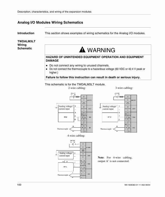
Description, characteristics, and wiring of the expansion modules
Analog I/O Modules Wiring Schematics
Introduction This section shows examples of wiring schematics for the Analog I/O modules.
TWDALM3LTWiringSchematic
This schematic is for the TWDALM3LT module.
WARNINGHAZARD OF UNINTENDED EQUIPMENT OPERATION AND EQUIPMENTDAMAGE
Do not connect any wiring to unused channels.Do not connect the thermocouple to a hazardous voltage (60 VDC or 42.4 V peak orhigher.)
Failure to follow this instruction can result in death or serious injury.
Analog voltage/current input
Thermocouple
Analog voltage/current input
Thermocouple
Analog voltage/current input
3-wire cabling:
4-wire cabling:
Note: For 4-wire cabling,output A’ is not connected.
Thermocouple
2-wire cabling:
100 W9 1606383 01 11 A02 09/04
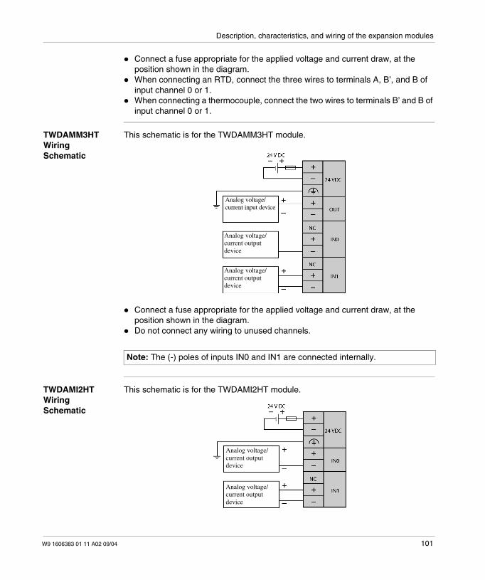
Description, characteristics, and wiring of the expansion modules
Connect a fuse appropriate for the applied voltage and current draw, at theposition shown in the diagram.When connecting an RTD, connect the three wires to terminals A, B’, and B ofinput channel 0 or 1.When connecting a thermocouple, connect the two wires to terminals B’ and B ofinput channel 0 or 1.
TWDAMM3HTWiringSchematic
This schematic is for the TWDAMM3HT module.
Connect a fuse appropriate for the applied voltage and current draw, at theposition shown in the diagram.Do not connect any wiring to unused channels.
TWDAMI2HTWiringSchematic
This schematic is for the TWDAMI2HT module.
Note: The (-) poles of inputs IN0 and IN1 are connected internally.
Analog voltage/current input device
Analog voltage/current outputdevice
Analog voltage/current outputdevice
Analog voltage/current outputdevice
Analog voltage/current outputdevice
W9 1606383 01 11 A02 09/04 101
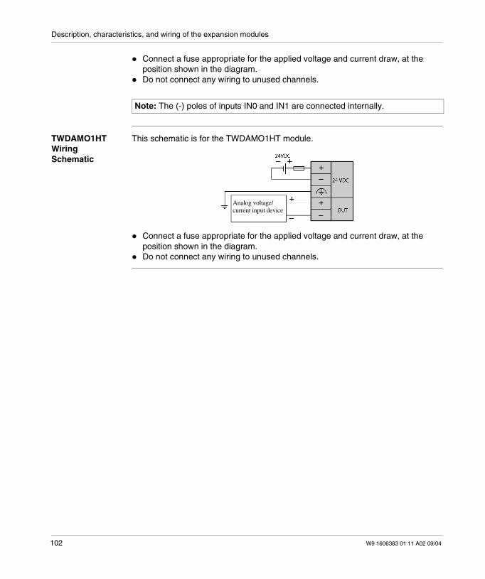
Description, characteristics, and wiring of the expansion modules
Connect a fuse appropriate for the applied voltage and current draw, at theposition shown in the diagram.Do not connect any wiring to unused channels.
TWDAMO1HTWiringSchematic
This schematic is for the TWDAMO1HT module.
Connect a fuse appropriate for the applied voltage and current draw, at theposition shown in the diagram.Do not connect any wiring to unused channels.
Note: The (-) poles of inputs IN0 and IN1 are connected internally.
Analog voltage/current input device
102 W9 1606383 01 11 A02 09/04
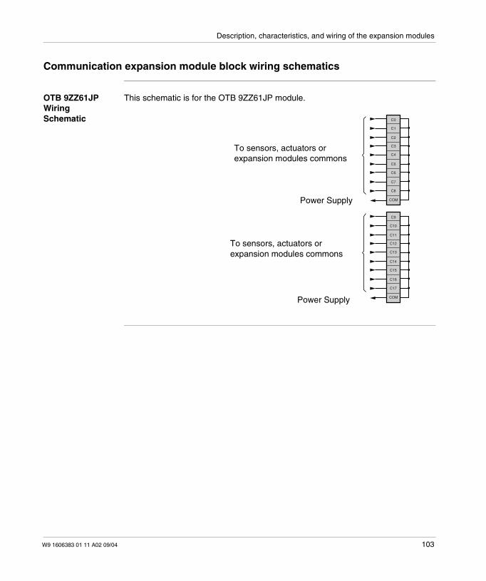
Description, characteristics, and wiring of the expansion modules
Communication expansion module block wiring schematics
OTB 9ZZ61JPWiringSchematic
This schematic is for the OTB 9ZZ61JP module.
C0
C1
C2
C3
C4
C5
C6
C7
C8
COM
C9
C10
C11
C12
C13
C14
C15
C16
C17
COM
To sensors, actuators orexpansion modules commons
Power Supply
To sensors, actuators orexpansion modules commons
Power Supply
W9 1606383 01 11 A02 09/04 103

Description, characteristics, and wiring of the expansion modules
104 W9 1606383 01 11 A02 09/04
W9 1606383 01 11 A02 09/04
5
Modbus Network Interface of theOTB ModuleAt a Glance
Introduction This chapter describes the external Modbus characteristics of the Advantys OTBnetwork interface module and the general Modbus features supported by themodule.
What's in thisChapter?
This chapter contains the following topics:
Topic Page
Description of the OTB Module Modbus Network Interface 106
Modbus Field Bus Interface 108
Network Node Address 112
Network Baud Rate 114
Modbus Configuration 116
Communication on a Modbus Network 117
Management of Island Behavior 120
Expansion module identification codes 124
105
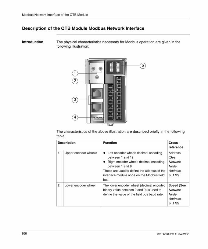
Modbus Network Interface of the OTB Module
Description of the OTB Module Modbus Network Interface
Introduction The physical characteristics necessary for Modbus operation are given in thefollowing illustration:
The characteristics of the above illustration are described briefly in the followingtable:
Description Function Cross-reference
1 Upper encoder wheels Left encoder wheel: decimal encodingbetween 1 and 12Right encoder wheel: decimal encodingbetween 1 and 9
These are used to define the address of theinterface module node on the Modbus fieldbus.
Address(SeeNetworkNodeAddress,p. 112)
2 Lower encoder wheel The lower encoder wheel (decimal encodedbinary value between 0 and 9) is used todefine the value of the field bus baud rate.
Speed (SeeNetworkNodeAddress,p. 112)
1
2
3
4
5
106 W9 1606383 01 11 A02 09/04
Modbus Network Interface of the OTB Module
3 Field bus interface Two eight-pin RJ45 connectors are used toconnect the interface module to a Modbusfield bus.
Interface(See ModbusField BusInterface,p. 108)
4 Electrical supplyinterface
Terminal for an external 24 VDC supply ofthe network interface module.
Supply (SeeHow toConnect thePowerSupply,p. 61)
5 Indicator LED The colored LEDs use various types ofdisplay to visually reflect the operationalstatus of the island bus.
IndicatorLED (SeeIndicatorLights(LEDs),p. 184)
Description Function Cross-reference
W9 1606383 01 11 A02 09/04 107
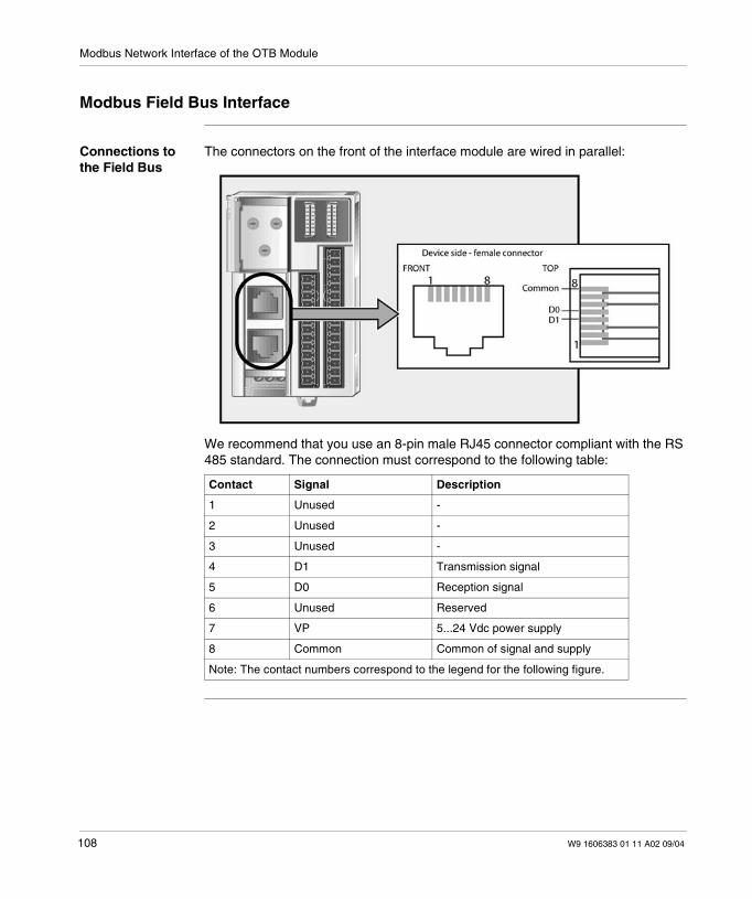
Modbus Network Interface of the OTB Module
Modbus Field Bus Interface
Connections tothe Field Bus
The connectors on the front of the interface module are wired in parallel:
We recommend that you use an 8-pin male RJ45 connector compliant with the RS485 standard. The connection must correspond to the following table:
Contact Signal Description
1 Unused -
2 Unused -
3 Unused -
4 D1 Transmission signal
5 D0 Reception signal
6 Unused Reserved
7 VP 5...24 Vdc power supply
8 Common Common of signal and supply
Note: The contact numbers correspond to the legend for the following figure.
108 W9 1606383 01 11 A02 09/04
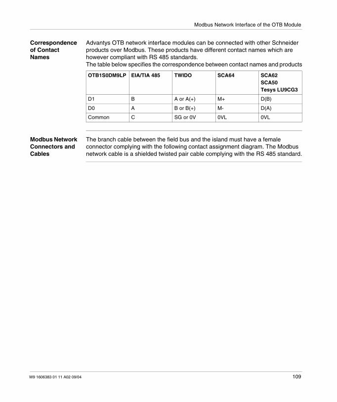
Modbus Network Interface of the OTB Module
Correspondenceof ContactNames
Advantys OTB network interface modules can be connected with other Schneiderproducts over Modbus. These products have different contact names which arehowever compliant with RS 485 standards.The table below specifies the correspondence between contact names and products
Modbus NetworkConnectors andCables
The branch cable between the field bus and the island must have a femaleconnector complying with the following contact assignment diagram. The Modbusnetwork cable is a shielded twisted pair cable complying with the RS 485 standard.
OTB1S0DM9LP EIA/TIA 485 TWIDO SCA64 SCA62SCA50Tesys LU9CG3
D1 B A or A(+) M+ D(B)
D0 A B or B(+) M- D(A)
Common C SG or 0V 0VL 0VL
W9 1606383 01 11 A02 09/04 109
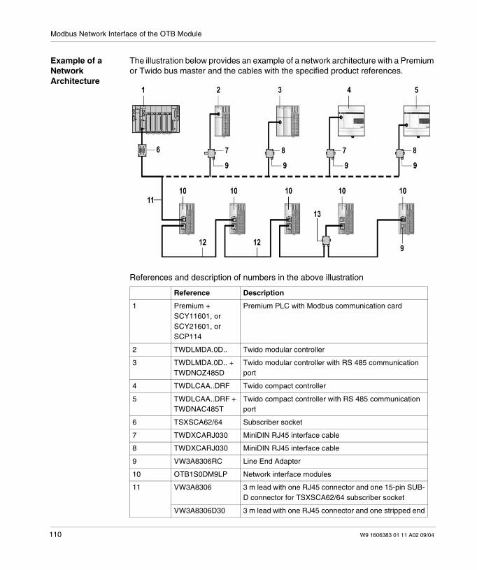
Modbus Network Interface of the OTB Module
Example of aNetworkArchitecture
The illustration below provides an example of a network architecture with a Premiumor Twido bus master and the cables with the specified product references.
References and description of numbers in the above illustration
Reference Description
1 Premium +SCY11601, orSCY21601, orSCP114
Premium PLC with Modbus communication card
2 TWDLMDA.0D.. Twido modular controller
3 TWDLMDA.0D.. +TWDNOZ485D
Twido modular controller with RS 485 communicationport
4 TWDLCAA..DRF Twido compact controller
5 TWDLCAA..DRF +TWDNAC485T
Twido compact controller with RS 485 communicationport
6 TSXSCA62/64 Subscriber socket
7 TWDXCARJ030 MiniDIN RJ45 interface cable
8 TWDXCARJ030 MiniDIN RJ45 interface cable
9 VW3A8306RC Line End Adapter
10 OTB1S0DM9LP Network interface modules
11 VW3A8306 3 m lead with one RJ45 connector and one 15-pin SUB-D connector for TSXSCA62/64 subscriber socket
VW3A8306D30 3 m lead with one RJ45 connector and one stripped end
110 W9 1606383 01 11 A02 09/04
Modbus Network Interface of the OTB Module
12 VW3A8306R03 0.3 m lead with 2 RJ45 connectors
VW3A8306R10 1 m lead with 2 RJ45 connectors
VW3A8306R30 3 m lead with 2 RJ45 connectors
13 VW3A8306TF03 T branch with 0.3 m cable
VW3A8306TF10 T branch with 1 m cable
Reference Description
W9 1606383 01 11 A02 09/04 111
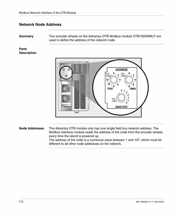
Modbus Network Interface of the OTB Module
Network Node Address
Summary Two encoder wheels on the Advantys OTB Modbus module OTB1S0DM9LP areused to define the address of the network node.
PartsDescription
Node Addresses The Advantys OTB module only has one single field bus network address. TheModbus interface module reads the address of the node from the encoder wheelsevery time the island is powered up.The address of the node is a numerical value between 1 and 127, which must bedifferent to all other node addresses on the network.
112 W9 1606383 01 11 A02 09/04
Modbus Network Interface of the OTB Module
Configuring theNode Address
The instructions for configuring the node address are described in the followingtable.
Field BusCommunication
The Advantys OTB interface module communicates when the encoder wheels areconfigured to a valid Modbus node address if the baud rate is the same as that ofthe system.If the island has a invalid node address, it cannot communicate with the master. Toestablish communication, configure the encoder wheels to a valid address andpower up the island.
Step Action Comment
1 Cut the power supply to the island. The changes you make will be detected onthe next power up.
2 Select the node address currentlyavailable on your field bus network.
The list of active nodes on the field busindicates which addresses are available.
3 Adjust the upper encoder wheelsLeft encoder wheel — 0 to 12 (tens)Right encoder wheel — 0 to 9(units)
Note that it is mechanically possible tospecify all node addresses from 00 to 129.However, address 00 is never used as aModbus node address and addresses 128and 129 are not operative.
4 Power up the island in order toimplement the new configuration.
The network interface module reads theencoder wheel adjustments only on powerup.
W9 1606383 01 11 A02 09/04 113
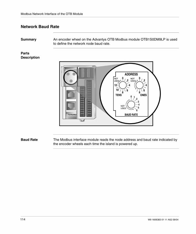
Modbus Network Interface of the OTB Module
Network Baud Rate
Summary An encoder wheel on the Advantys OTB Modbus module OTB1S0DM9LP is usedto define the network node baud rate.
PartsDescription
Baud Rate The Modbus interface module reads the node address and baud rate indicated bythe encoder wheels each time the island is powered up.
114 W9 1606383 01 11 A02 09/04
Modbus Network Interface of the OTB Module
Configuration ofBaud Rate
The instructions for configuring the baud rate of the module are given in the followingtable:
Baud RateSelection Table
.
Step Action Comment
1 Cut the power supply to the island. The changes you make will be detected onthe next power up.
2 Select the baud rate to be used for fieldbus communications.
The baud rate configuration depends onthe specifications of your system and thenetwork.
3 Set the lower encoder wheel to theposition corresponding to the requiredbaud rate.
Use the following baud rate selection table.
4 Power up the island in order toimplement the new configuration.
The network interface module reads theencoder wheel parameters only on powerup.
Position (lower encoderrate)
Baud Rate
0 19200 bits/s
1 1200 bits/s
2 2400 bits/s
3 4800 bits/s
4 9600 bits/s
5 19200 bits/s
6 38400 bits/s
W9 1606383 01 11 A02 09/04 115
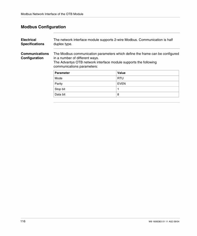
Modbus Network Interface of the OTB Module
Modbus Configuration
ElectricalSpecifications
The network interface module supports 2-wire Modbus. Communication is halfduplex type.
CommunicationsConfiguration
The Modbus communication parameters which define the frame can be configuredin a number of different ways.The Advantys OTB network interface module supports the followingcommunications parameters:
Parameter Value
Mode RTU
Parity EVEN
Stop bit 1
Data bit 8
116 W9 1606383 01 11 A02 09/04
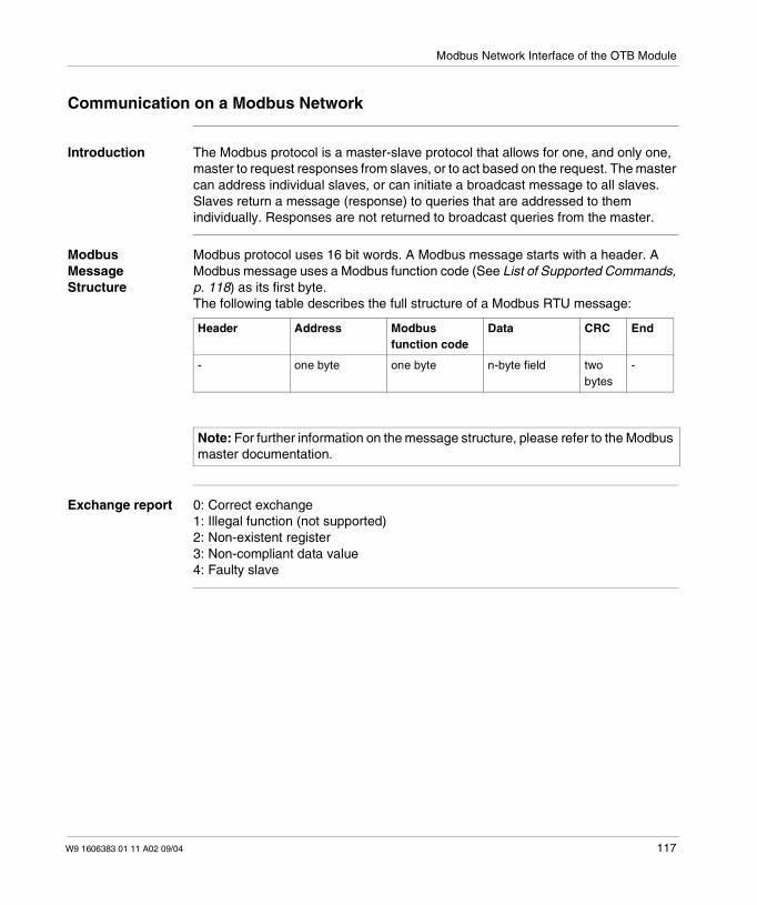
Modbus Network Interface of the OTB Module
Communication on a Modbus Network
Introduction The Modbus protocol is a master-slave protocol that allows for one, and only one,master to request responses from slaves, or to act based on the request. The mastercan address individual slaves, or can initiate a broadcast message to all slaves.Slaves return a message (response) to queries that are addressed to themindividually. Responses are not returned to broadcast queries from the master.
ModbusMessageStructure
Modbus protocol uses 16 bit words. A Modbus message starts with a header. AModbus message uses a Modbus function code (See List of Supported Commands,p. 118) as its first byte.The following table describes the full structure of a Modbus RTU message:
Exchange report 0: Correct exchange1: Illegal function (not supported)2: Non-existent register3: Non-compliant data value4: Faulty slave
Header Address Modbusfunction code
Data CRC End
- one byte one byte n-byte field twobytes
-
Note: For further information on the message structure, please refer to the Modbusmaster documentation.
W9 1606383 01 11 A02 09/04 117
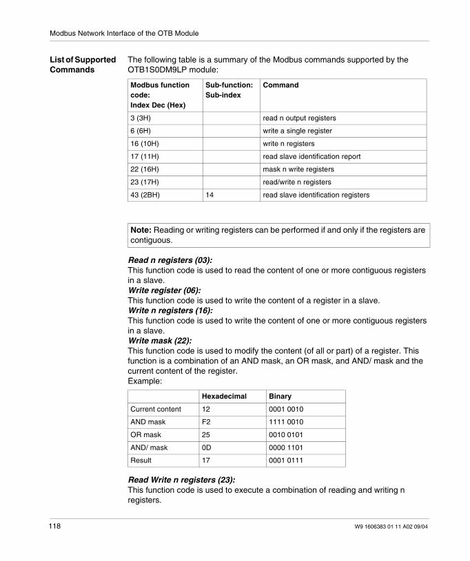
Modbus Network Interface of the OTB Module
List of SupportedCommands
The following table is a summary of the Modbus commands supported by theOTB1S0DM9LP module:
Read n registers (03):This function code is used to read the content of one or more contiguous registersin a slave.Write register (06):This function code is used to write the content of a register in a slave.Write n registers (16):This function code is used to write the content of one or more contiguous registersin a slave.Write mask (22):This function code is used to modify the content (of all or part) of a register. Thisfunction is a combination of an AND mask, an OR mask, and AND/ mask and thecurrent content of the register.Example:
Read Write n registers (23):This function code is used to execute a combination of reading and writing nregisters.
Modbus functioncode:Index Dec (Hex)
Sub-function:Sub-index
Command
3 (3H) read n output registers
6 (6H) write a single register
16 (10H) write n registers
17 (11H) read slave identification report
22 (16H) mask n write registers
23 (17H) read/write n registers
43 (2BH) 14 read slave identification registers
Note: Reading or writing registers can be performed if and only if the registers arecontiguous.
Hexadecimal Binary
Current content 12 0001 0010
AND mask F2 1111 0010
OR mask 25 0010 0101
AND/ mask 0D 0000 1101
Result 17 0001 0111
118 W9 1606383 01 11 A02 09/04
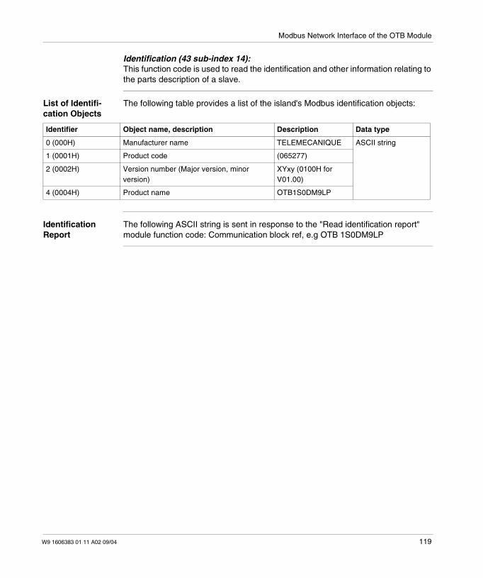
Modbus Network Interface of the OTB Module
Identification (43 sub-index 14):This function code is used to read the identification and other information relating tothe parts description of a slave.
List of Identifi-cation Objects
The following table provides a list of the island's Modbus identification objects:
IdentificationReport
The following ASCII string is sent in response to the "Read identification report"module function code: Communication block ref, e.g OTB 1S0DM9LP
Identifier Object name, description Description Data type
0 (000H) Manufacturer name TELEMECANIQUE ASCII string
1 (0001H) Product code (065277)
2 (0002H) Version number (Major version, minorversion)
XYxy (0100H forV01.00)
4 (0004H) Product name OTB1S0DM9LP
W9 1606383 01 11 A02 09/04 119
Modbus Network Interface of the OTB Module
Management of Island Behavior
Configuration ofAnalogExpansionModules
To configure analog expansion modules, you must stop activity on the island'sinternal bus by writing the value 1 to the register 1005.Once the configuration parameters of the expansion modules have been updated,the content of the object 1005 must be reset to 0 to resume activity on the internalbus with the new parameters.
32 Bit Function The function of the register 1008 is to define the order of 32 bit information. It canonly be used for parameters in 32 bit format. Its default value is 0 (MSB/LSB).Register 1008 - Bit 0 = 0The registers concerned by 32 bit format are in MSB/LSB format.Register 1008 - Bit 0 = 1The registers concerned by 32 bit format are in MSB/LSB format.
Setting NetworkMonitoringTimes
The register 1006 is used to set the monitoring time in ms.Values for register 1006
0: no network monitoring (default value)x: monitoring time in ms (1 to 65535 ms)
Note: The expansion module outputs are deactivated and switch to zero when thisoperation is performed.
Note: If a parameter is non-compliant (invalid configuration), it is impossible towrite zero to the register 1005.
120 W9 1606383 01 11 A02 09/04
Modbus Network Interface of the OTB Module
NetworkMonitoring
The island goes into fallback mode if the connection to the network is lost or if noclient is present on the network.If no frame is detected on the network before the monitoring time expires, the islanddetects that the client has disconnected. The outputs and special function switch tothe fallback value defined by the user.Bit 9 of register 900 switches to 1.Writing the value 0 to the command register 1007 enables you to set bit 9 of register900 to zero in order to resume network monitoring.
CAUTIONFALLBACK MODE AFTER DISCONNECTION
It is possible to write to outputs once reconnected without the need foracknowledgement.
Failure to follow this instruction can result in injury.
W9 1606383 01 11 A02 09/04 121
Modbus Network Interface of the OTB Module
Saving andRestoringParameters
InitializationAn OTB module is initialized with default parameters. When detected by the busmaster, the OTB module is configured with the parameters defined in theconfiguration tool. These parameters must be backed-up in order to beacknowledged the next time the system is started.Current parametersRegister 1000 indicates the current set of parameters:
0: the island is using the default parameter set (factory settings)1: the island is using the last saved parameter set2: one or more parameters have been modified since the last backup or startup.
Saving parametersThe back-up operation is performed by modifying the value of register 1002.This saves the current parameters of the OTB module and tells it to use these savedparameters on future start-ups.A backup counter is available in register 1001. This counter is reset to 0 when factorysettings are restored.
Note: The backed up registers correspond to the parameter registers of thedifferent zones.When a backup is in progress, the module stops communication for 300 ms andthe expansion module outputs switch to 0.
122 W9 1606383 01 11 A02 09/04
Modbus Network Interface of the OTB Module
Restoring parametersThe different possible restores are described in the following table:
Identification ofIsland Modules
The following table describes the mapping of descriptions of modules on the island
To restore... you must modify the value of theregister...
the last backed upconfiguration
1003
the factory settings 1004
Registers Functions Object code
1100 OTB product code FEFDH
1101 OTB software version XYxy
1102 Type of expansion module 1 (1)
1103 Type of expansion module 2 (1)
1104 Type of expansion module 3 (1)
1105 Type of expansion module 4 (1)
1106 Type of expansion module 5 (1)
1107 Type of expansion module 6 (1)
1108 Type of expansion module 7 (1)
Note: (1) depending on the type of expansion module connected. See the table ofExpansion Module Identification Codes. The default value is equal to FFFFH
W9 1606383 01 11 A02 09/04 123
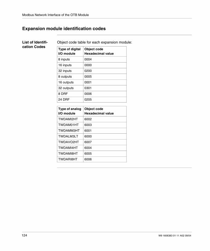
Modbus Network Interface of the OTB Module
Expansion module identification codes
List of Identifi-cation Codes
Object code table for each expansion module:
Type of digitalI/O module
Object codeHexadecimal value
8 inputs 0004
16 inputs 0000
32 inputs 0200
8 outputs 0005
16 outputs 0001
32 outputs 0301
8 DRF 0006
24 DRF 0205
Type of analogI/O module
Object codeHexadecimal value
TWDAMI2HT 6002
TWDAM01HT 6003
TWDAMM3HT 6001
TWDALM3LT 6000
TWDAVO2HT 6007
TWDAMI4HT 6004
TWDAMI8HT 6005
TWDARI8HT 6006
124 W9 1606383 01 11 A02 09/04
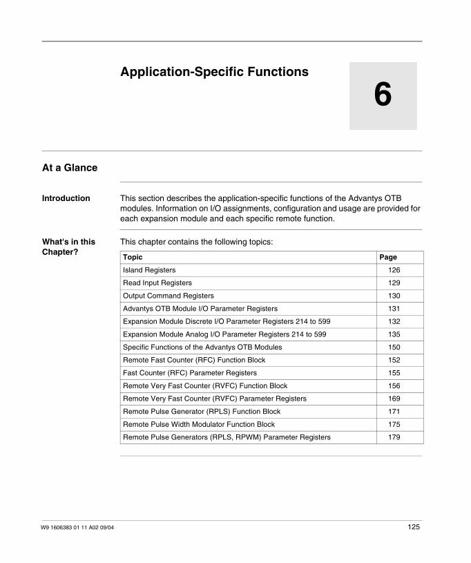
W9 1606383 01 11 A02 09/04
6
Application-Specific FunctionsAt a Glance
Introduction This section describes the application-specific functions of the Advantys OTBmodules. Information on I/O assignments, configuration and usage are provided foreach expansion module and each specific remote function.
What's in thisChapter?
This chapter contains the following topics:
Topic Page
Island Registers 126
Read Input Registers 129
Output Command Registers 130
Advantys OTB Module I/O Parameter Registers 131
Expansion Module Discrete I/O Parameter Registers 214 to 599 132
Expansion Module Analog I/O Parameter Registers 214 to 599 135
Specific Functions of the Advantys OTB Modules 150
Remote Fast Counter (RFC) Function Block 152
Fast Counter (RFC) Parameter Registers 155
Remote Very Fast Counter (RVFC) Function Block 156
Remote Very Fast Counter (RVFC) Parameter Registers 169
Remote Pulse Generator (RPLS) Function Block 171
Remote Pulse Width Modulator Function Block 175
Remote Pulse Generators (RPLS, RPWM) Parameter Registers 179
125
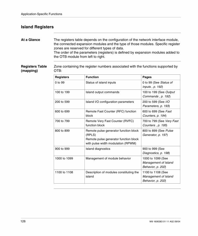
Application-Specific Functions
Island Registers
At a Glance The registers table depends on the configuration of the network interface module,the connected expansion modules and the type of those modules. Specific registerzones are reserved for different types of data.The order of the parameters (registers) is defined by expansion modules added tothe OTB module from left to right.
Registers Table(mapping)
Zone containing the register numbers associated with the functions supported byOTB:
Registers Function Pages
0 to 99 Status of island inputs 0 to 99 (See Status ofinputs , p. 192)
100 to 199 Island output commands 100 to 199 (See OutputCommands , p. 192)
200 to 599 Island I/O configuration parameters 200 to 599 (See I/OParameters, p. 193)
600 to 699 Remote Fast Counter (RFC) functionblock
600 to 699 (See FastCounters, p. 194)
700 to 799 Remote Very Fast Counter (RVFC)function block
700 to 799 (See Very FastCounters , p. 195)
800 to 899 Remote pulse generator function block(RPLS)Remote pulse generator function blockwith pulse width modulation (RPWM)
800 to 899 (See PulseGenerator, p. 197)
900 to 999 Island diagnostics 900 to 999 (SeeDiagnostics, p. 198)
1000 to 1099 Management of module behavior 1000 to 1099 (SeeManagement of IslandBehavior, p. 202)
1100 to 1108 Description of modules constituting theisland
1100 to 1108 (SeeManagement of IslandBehavior, p. 202)
126 W9 1606383 01 11 A02 09/04

Application-Specific Functions
OTB ModuleRegisters
For each application-specific function, the OTB network interface module uses thenumber of registers indicated in the following table:
Status ofinputs
Outputcommands
Parameters RFC RVFC RPLSRPWM
Diagnostics Modulebehavior
0 to 99 100 to 199 200 to 599 600 to 699 700 to 799 800 to 899 900 to 999 1000 to 1099
1 1 14 8 percounter
14 per counter 10 pergenerator
11 6
W9 1606383 01 11 A02 09/04 127
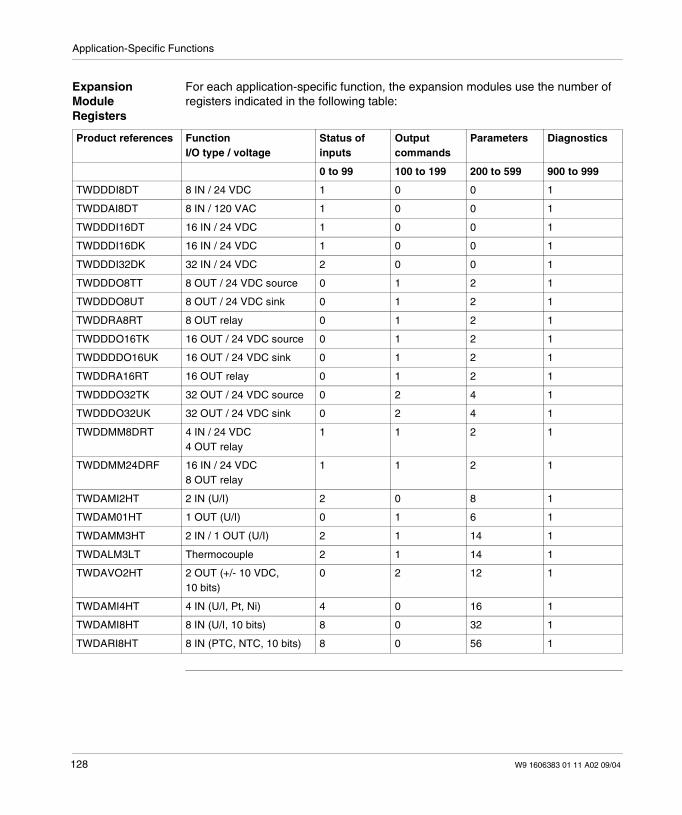
Application-Specific Functions
ExpansionModuleRegisters
For each application-specific function, the expansion modules use the number ofregisters indicated in the following table:
Product references FunctionI/O type / voltage
Status ofinputs
Outputcommands
Parameters Diagnostics
0 to 99 100 to 199 200 to 599 900 to 999
TWDDDI8DT 8 IN / 24 VDC 1 0 0 1
TWDDAI8DT 8 IN / 120 VAC 1 0 0 1
TWDDDI16DT 16 IN / 24 VDC 1 0 0 1
TWDDDI16DK 16 IN / 24 VDC 1 0 0 1
TWDDDI32DK 32 IN / 24 VDC 2 0 0 1
TWDDDO8TT 8 OUT / 24 VDC source 0 1 2 1
TWDDDO8UT 8 OUT / 24 VDC sink 0 1 2 1
TWDDRA8RT 8 OUT relay 0 1 2 1
TWDDDO16TK 16 OUT / 24 VDC source 0 1 2 1
TWDDDDO16UK 16 OUT / 24 VDC sink 0 1 2 1
TWDDRA16RT 16 OUT relay 0 1 2 1
TWDDDO32TK 32 OUT / 24 VDC source 0 2 4 1
TWDDDO32UK 32 OUT / 24 VDC sink 0 2 4 1
TWDDMM8DRT 4 IN / 24 VDC4 OUT relay
1 1 2 1
TWDDMM24DRF 16 IN / 24 VDC8 OUT relay
1 1 2 1
TWDAMI2HT 2 IN (U/I) 2 0 8 1
TWDAM01HT 1 OUT (U/I) 0 1 6 1
TWDAMM3HT 2 IN / 1 OUT (U/I) 2 1 14 1
TWDALM3LT Thermocouple 2 1 14 1
TWDAVO2HT 2 OUT (+/- 10 VDC,10 bits)
0 2 12 1
TWDAMI4HT 4 IN (U/I, Pt, Ni) 4 0 16 1
TWDAMI8HT 8 IN (U/I, 10 bits) 8 0 32 1
TWDARI8HT 8 IN (PTC, NTC, 10 bits) 8 0 56 1
128 W9 1606383 01 11 A02 09/04
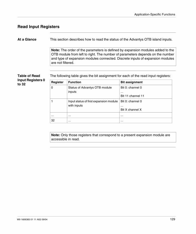
Application-Specific Functions
Read Input Registers
At a Glance This section describes how to read the status of the Advantys OTB island inputs.
Table of ReadInput Registers 0to 32
The following table gives the bit assignment for each of the read input registers:
Note: The order of the parameters is defined by expansion modules added to theOTB module from left to right. The number of parameters depends on the numberand type of expansion modules connected. Discrete inputs of expansion modulesare not filtered.
Register Function Bit assignment
0 Status of Advantys OTB moduleinputs
Bit 0: channel 0...Bit 11 channel 11
1 Input status of first expansion modulewith inputs
Bit 0: channel 0...Bit X channel X
... ... ...
32 ... ...
Note: Only those registers that correspond to a present expansion module areaccessible in read.
W9 1606383 01 11 A02 09/04 129
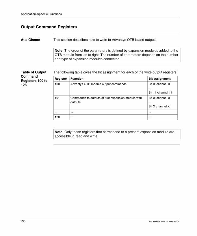
Application-Specific Functions
Output Command Registers
At a Glance This section describes how to write to Advantys OTB island outputs.
Table of OutputCommandRegisters 100 to128
The following table gives the bit assignment for each of the write output registers:
Note: The order of the parameters is defined by expansion modules added to theOTB module from left to right. The number of parameters depends on the numberand type of expansion modules connected.
Register Function Bit assignment
100 Advantys OTB module output commands Bit 0: channel 0...Bit 11 channel 11
101 Commands to outputs of first expansion module withoutputs
Bit 0: channel 0...Bit X channel X
... ... ...
128 ... ...
Note: Only those registers that correspond to a present expansion module areaccessible in read and write.
130 W9 1606383 01 11 A02 09/04
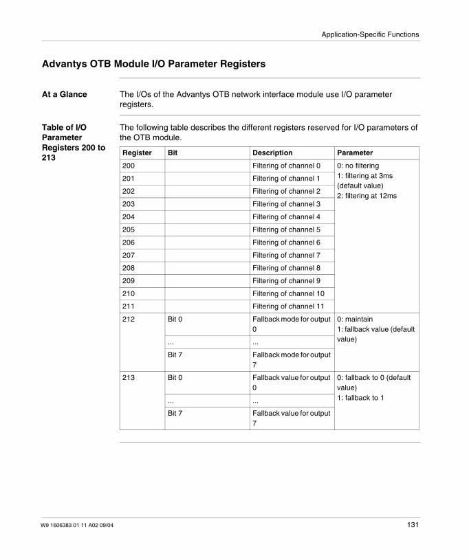
Application-Specific Functions
Advantys OTB Module I/O Parameter Registers
At a Glance The I/Os of the Advantys OTB network interface module use I/O parameterregisters.
Table of I/OParameterRegisters 200 to213
The following table describes the different registers reserved for I/O parameters ofthe OTB module.
Register Bit Description Parameter
200 Filtering of channel 0 0: no filtering1: filtering at 3ms(default value)2: filtering at 12ms
201 Filtering of channel 1
202 Filtering of channel 2
203 Filtering of channel 3
204 Filtering of channel 4
205 Filtering of channel 5
206 Filtering of channel 6
207 Filtering of channel 7
208 Filtering of channel 8
209 Filtering of channel 9
210 Filtering of channel 10
211 Filtering of channel 11
212 Bit 0 Fallback mode for output0
0: maintain1: fallback value (defaultvalue)... ...
Bit 7 Fallback mode for output7
213 Bit 0 Fallback value for output0
0: fallback to 0 (defaultvalue)1: fallback to 1... ...
Bit 7 Fallback value for output7
W9 1606383 01 11 A02 09/04 131
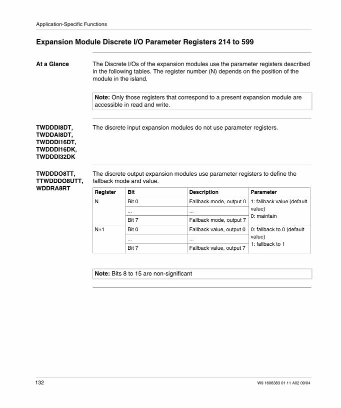
Application-Specific Functions
Expansion Module Discrete I/O Parameter Registers 214 to 599
At a Glance The Discrete I/Os of the expansion modules use the parameter registers describedin the following tables. The register number (N) depends on the position of themodule in the island.
TWDDDI8DT,TWDDAI8DT,TWDDDI16DT,TWDDDI16DK,TWDDDI32DK
The discrete input expansion modules do not use parameter registers.
TWDDDO8TT,TTWDDDO8UTT,WDDRA8RT
The discrete output expansion modules use parameter registers to define thefallback mode and value.
Note: Only those registers that correspond to a present expansion module areaccessible in read and write.
Register Bit Description Parameter
N Bit 0 Fallback mode, output 0 1: fallback value (defaultvalue)0: maintain
... ...
Bit 7 Fallback mode, output 7
N+1 Bit 0 Fallback value, output 0 0: fallback to 0 (defaultvalue)1: fallback to 1
... ...
Bit 7 Fallback value, output 7
Note: Bits 8 to 15 are non-significant
132 W9 1606383 01 11 A02 09/04
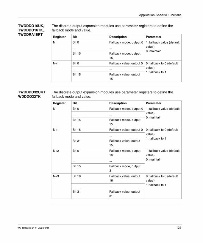
Application-Specific Functions
TWDDDO16UK,TWDDDO16TK,TWDDRA16RT
The discrete output expansion modules use parameter registers to define thefallback mode and value.
TWDDDO32UKTWDDDO32TK
The discrete output expansion modules use parameter registers to define thefallback mode and value.
Register Bit Description Parameter
N Bit 0 Fallback mode, output 0 1: fallback value (defaultvalue)0: maintain
... ...
Bit 15 Fallback mode, output15
N+1 Bit 0 Fallback value, output 0 0: fallback to 0 (defaultvalue)1: fallback to 1
... ...
Bit 15 Fallback value, output15
Register Bit Description Parameter
N Bit 0 Fallback mode, output 0 1: fallback value (defaultvalue)0: maintain
... ...
Bit 15 Fallback mode, output15
N+1 Bit 16 Fallback value, output 0 0: fallback to 0 (defaultvalue)1: fallback to 1
... ...
Bit 31 Fallback value, output15
N+2 Bit 0 Fallback mode, output16
1: fallback value (defaultvalue)0: maintain... ...
Bit 15 Fallback mode, output31
N+3 Bit 16 Fallback value, output16
0: fallback to 0 (defaultvalue)1: fallback to 1... ...
Bit 31 Fallback value, output31
W9 1606383 01 11 A02 09/04 133
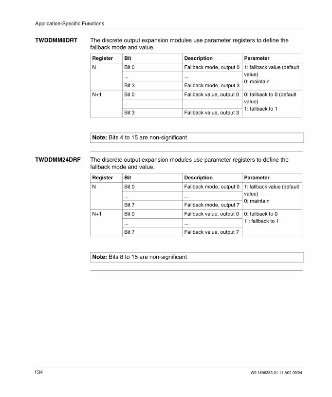
Application-Specific Functions
TWDDMM8DRT The discrete output expansion modules use parameter registers to define thefallback mode and value.
TWDDMM24DRF The discrete output expansion modules use parameter registers to define thefallback mode and value.
Register Bit Description Parameter
N Bit 0 Fallback mode, output 0 1: fallback value (defaultvalue)0: maintain
... ...
Bit 3 Fallback mode, output 3
N+1 Bit 0 Fallback value, output 0 0: fallback to 0 (defaultvalue)1: fallback to 1
... ...
Bit 3 Fallback value, output 3
Note: Bits 4 to 15 are non-significant
Register Bit Description Parameter
N Bit 0 Fallback mode, output 0 1: fallback value (defaultvalue)0: maintain
... ...
Bit 7 Fallback mode, output 7
N+1 Bit 0 Fallback value, output 0 0: fallback to 01 : fallback to 1... ...
Bit 7 Fallback value, output 7
Note: Bits 8 to 15 are non-significant
134 W9 1606383 01 11 A02 09/04
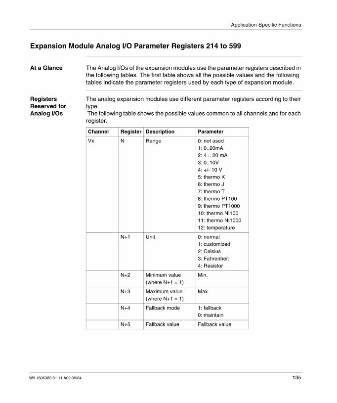
Application-Specific Functions
Expansion Module Analog I/O Parameter Registers 214 to 599
At a Glance The Analog I/Os of the expansion modules use the parameter registers described inthe following tables. The first table shows all the possible values and the followingtables indicate the parameter registers used by each type of expansion module.
RegistersReserved forAnalog I/Os
The analog expansion modules use different parameter registers according to theirtype.The following table shows the possible values common to all channels and for eachregister.
Channel Register Description Parameter
Vx N Range 0: not used1: 0..20mA2: 4 .. 20 mA3: 0..10V4: +/- 10 V5: thermo K6: thermo J7: thermo T8: thermo PT1009: thermo PT100010: thermo NI10011: thermo NI100012: temperature
N+1 Unit 0: normal1: customized2: Celsius3: Fahrenheit4: Resistor
N+2 Minimum value(where N+1 = 1)
Min.
N+3 Maximum value(where N+1 = 1)
Max.
N+4 Fallback mode 1: fallback0: maintain
N+5 Fallback value Fallback value
W9 1606383 01 11 A02 09/04 135
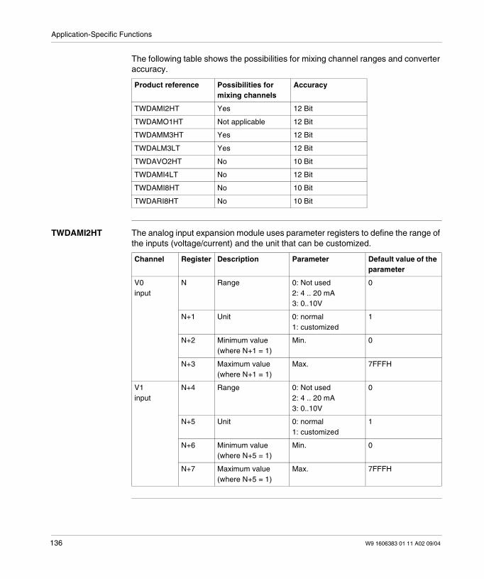
Application-Specific Functions
The following table shows the possibilities for mixing channel ranges and converteraccuracy.
TWDAMI2HT The analog input expansion module uses parameter registers to define the range ofthe inputs (voltage/current) and the unit that can be customized.
Product reference Possibilities formixing channels
Accuracy
TWDAMI2HT Yes 12 Bit
TWDAMO1HT Not applicable 12 Bit
TWDAMM3HT Yes 12 Bit
TWDALM3LT Yes 12 Bit
TWDAVO2HT No 10 Bit
TWDAMI4LT No 12 Bit
TWDAMI8HT No 10 Bit
TWDARI8HT No 10 Bit
Channel Register Description Parameter Default value of theparameter
V0input
N Range 0: Not used2: 4 .. 20 mA3: 0..10V
0
N+1 Unit 0: normal1: customized
1
N+2 Minimum value(where N+1 = 1)
Min. 0
N+3 Maximum value(where N+1 = 1)
Max. 7FFFH
V1input
N+4 Range 0: Not used2: 4 .. 20 mA3: 0..10V
0
N+5 Unit 0: normal1: customized
1
N+6 Minimum value(where N+5 = 1)
Min. 0
N+7 Maximum value(where N+5 = 1)
Max. 7FFFH
136 W9 1606383 01 11 A02 09/04
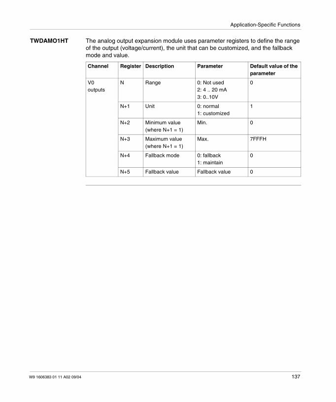
Application-Specific Functions
TWDAMO1HT The analog output expansion module uses parameter registers to define the rangeof the output (voltage/current), the unit that can be customized, and the fallbackmode and value.
Channel Register Description Parameter Default value of theparameter
V0outputs
N Range 0: Not used2: 4 .. 20 mA3: 0..10V
0
N+1 Unit 0: normal1: customized
1
N+2 Minimum value(where N+1 = 1)
Min. 0
N+3 Maximum value(where N+1 = 1)
Max. 7FFFH
N+4 Fallback mode 0: fallback1: maintain
0
N+5 Fallback value Fallback value 0
W9 1606383 01 11 A02 09/04 137
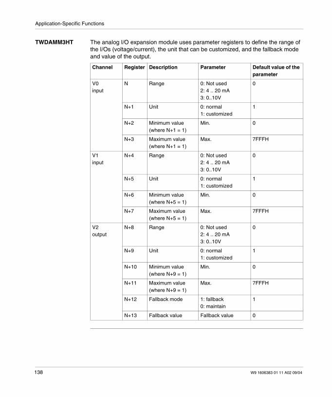
Application-Specific Functions
TWDAMM3HT The analog I/O expansion module uses parameter registers to define the range ofthe I/Os (voltage/current), the unit that can be customized, and the fallback modeand value of the output.
Channel Register Description Parameter Default value of theparameter
V0input
N Range 0: Not used2: 4 .. 20 mA3: 0..10V
0
N+1 Unit 0: normal1: customized
1
N+2 Minimum value(where N+1 = 1)
Min. 0
N+3 Maximum value(where N+1 = 1)
Max. 7FFFH
V1input
N+4 Range 0: Not used2: 4 .. 20 mA3: 0..10V
0
N+5 Unit 0: normal1: customized
1
N+6 Minimum value(where N+5 = 1)
Min. 0
N+7 Maximum value(where N+5 = 1)
Max. 7FFFH
V2output
N+8 Range 0: Not used2: 4 .. 20 mA3: 0..10V
0
N+9 Unit 0: normal1: customized
1
N+10 Minimum value(where N+9 = 1)
Min. 0
N+11 Maximum value(where N+9 = 1)
Max. 7FFFH
N+12 Fallback mode 1: fallback0: maintain
1
N+13 Fallback value Fallback value 0
138 W9 1606383 01 11 A02 09/04
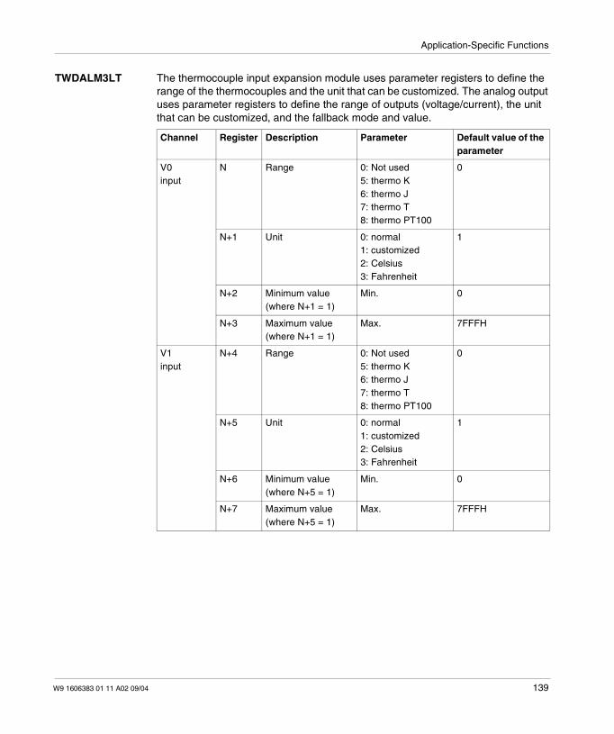
Application-Specific Functions
TWDALM3LT The thermocouple input expansion module uses parameter registers to define therange of the thermocouples and the unit that can be customized. The analog outputuses parameter registers to define the range of outputs (voltage/current), the unitthat can be customized, and the fallback mode and value.
Channel Register Description Parameter Default value of theparameter
V0input
N Range 0: Not used5: thermo K6: thermo J7: thermo T8: thermo PT100
0
N+1 Unit 0: normal1: customized2: Celsius3: Fahrenheit
1
N+2 Minimum value(where N+1 = 1)
Min. 0
N+3 Maximum value(where N+1 = 1)
Max. 7FFFH
V1input
N+4 Range 0: Not used5: thermo K6: thermo J7: thermo T8: thermo PT100
0
N+5 Unit 0: normal1: customized2: Celsius3: Fahrenheit
1
N+6 Minimum value(where N+5 = 1)
Min. 0
N+7 Maximum value(where N+5 = 1)
Max. 7FFFH
W9 1606383 01 11 A02 09/04 139
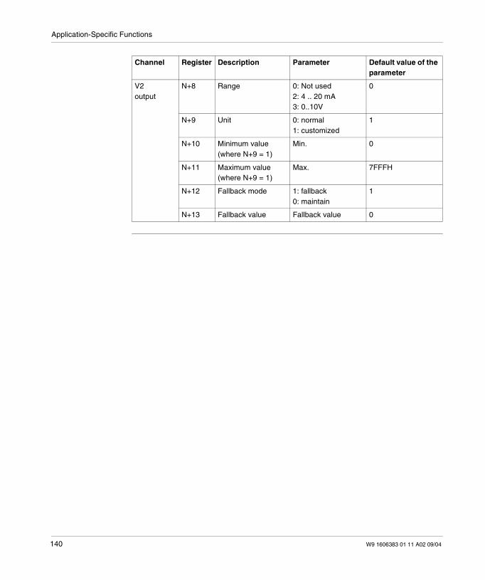
Application-Specific Functions
V2output
N+8 Range 0: Not used2: 4 .. 20 mA3: 0..10V
0
N+9 Unit 0: normal1: customized
1
N+10 Minimum value(where N+9 = 1)
Min. 0
N+11 Maximum value(where N+9 = 1)
Max. 7FFFH
N+12 Fallback mode 1: fallback0: maintain
1
N+13 Fallback value Fallback value 0
Channel Register Description Parameter Default value of theparameter
140 W9 1606383 01 11 A02 09/04
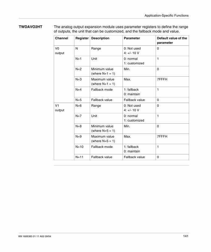
Application-Specific Functions
TWDAVO2HT The analog output expansion module uses parameter registers to define the rangeof outputs, the unit that can be customized, and the fallback mode and value.
Channel Register Description Parameter Default value of theparameter
V0output
N Range 0: Not used4: +/- 10 V
0
N+1 Unit 0: normal1: customized
1
N+2 Minimum value(where N+1 = 1)
Min. 0
N+3 Maximum value(where N+1 = 1)
Max. 7FFFH
N+4 Fallback mode 1: fallback0: maintain
1
N+5 Fallback value Fallback value 0
V1output
N+6 Range 0: Not used4: +/- 10 V
0
N+7 Unit 0: normal1: customized
1
N+8 Minimum value(where N+5 = 1)
Min. 0
N+9 Maximum value(where N+5 = 1)
Max. 7FFFH
N+10 Fallback mode 1: fallback0: maintain
1
N+11 Fallback value Fallback value 0
W9 1606383 01 11 A02 09/04 141
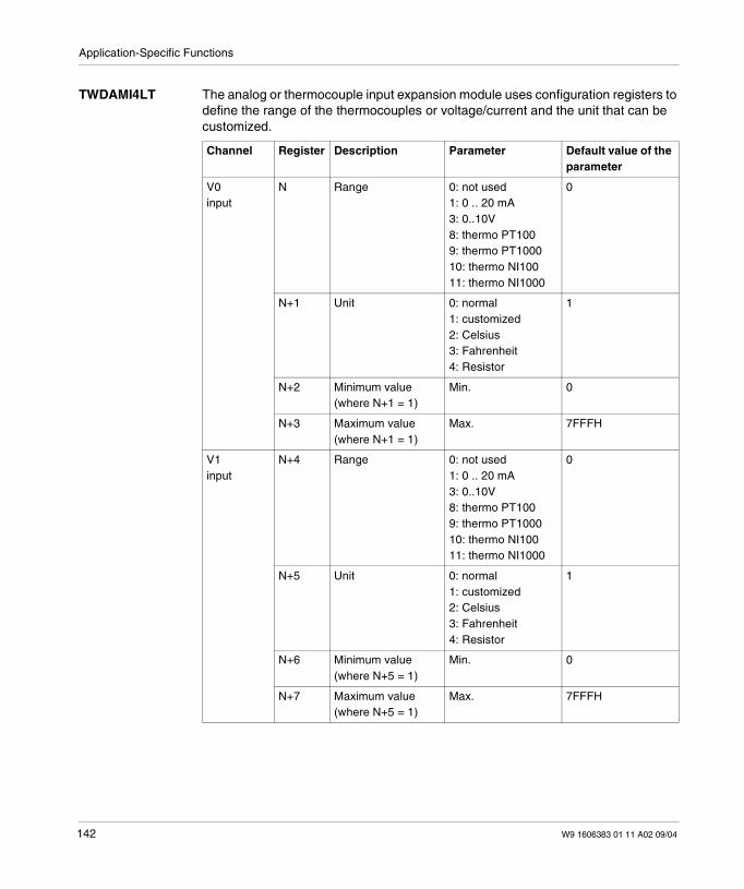
Application-Specific Functions
TWDAMI4LT The analog or thermocouple input expansion module uses configuration registers todefine the range of the thermocouples or voltage/current and the unit that can becustomized.
Channel Register Description Parameter Default value of theparameter
V0input
N Range 0: not used1: 0 .. 20 mA3: 0..10V8: thermo PT1009: thermo PT100010: thermo NI10011: thermo NI1000
0
N+1 Unit 0: normal1: customized2: Celsius3: Fahrenheit4: Resistor
1
N+2 Minimum value(where N+1 = 1)
Min. 0
N+3 Maximum value(where N+1 = 1)
Max. 7FFFH
V1input
N+4 Range 0: not used1: 0 .. 20 mA3: 0..10V8: thermo PT1009: thermo PT100010: thermo NI10011: thermo NI1000
0
N+5 Unit 0: normal1: customized2: Celsius3: Fahrenheit4: Resistor
1
N+6 Minimum value(where N+5 = 1)
Min. 0
N+7 Maximum value(where N+5 = 1)
Max. 7FFFH
142 W9 1606383 01 11 A02 09/04
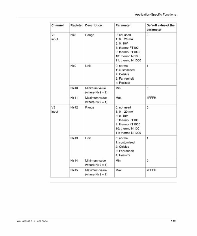
Application-Specific Functions
V2input
N+8 Range 0: not used1: 0 .. 20 mA3: 0..10V8: thermo PT1009: thermo PT100010: thermo NI10011: thermo NI1000
0
N+9 Unit 0: normal1: customized2: Celsius3: Fahrenheit4: Resistor
1
N+10 Minimum value(where N+9 = 1)
Min. 0
N+11 Maximum value(where N+9 = 1)
Max. 7FFFH
V3input
N+12 Range 0: not used1: 0 .. 20 mA3: 0..10V8: thermo PT1009: thermo PT100010: thermo NI10011: thermo NI1000
0
N+13 Unit 0: normal1: customized2: Celsius3: Fahrenheit4: Resistor
1
N+14 Minimum value(where N+9 = 1)
Min. 0
N+15 Maximum value(where N+9 = 1)
Max. 7FFFH
Channel Register Description Parameter Default value of theparameter
W9 1606383 01 11 A02 09/04 143
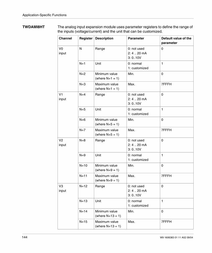
Application-Specific Functions
TWDAMI8HT The analog input expansion module uses parameter registers to define the range ofthe inputs (voltage/current) and the unit that can be customized.
Channel Register Description Parameter Default value of theparameter
V0input
N Range 0: not used2: 4 .. 20 mA3: 0..10V
0
N+1 Unit 0: normal1: customized
1
N+2 Minimum value(where N+1 = 1)
Min. 0
N+3 Maximum value(where N+1 = 1)
Max. 7FFFH
V1input
N+4 Range 0: not used2: 4 .. 20 mA3: 0..10V
0
N+5 Unit 0: normal1: customized
1
N+6 Minimum value(where N+5 = 1)
Min. 0
N+7 Maximum value(where N+5 = 1)
Max. 7FFFH
V2input
N+8 Range 0: not used2: 4 .. 20 mA3: 0..10V
0
N+9 Unit 0: normal1: customized
1
N+10 Minimum value(where N+9 = 1)
Min. 0
N+11 Maximum value(where N+9 = 1)
Max. 7FFFH
V3input
N+12 Range 0: not used2: 4 .. 20 mA3: 0..10V
0
N+13 Unit 0: normal1: customized
1
N+14 Minimum value(where N+13 = 1)
Min. 0
N+15 Maximum value(where N+13 = 1)
Max. 7FFFH
144 W9 1606383 01 11 A02 09/04
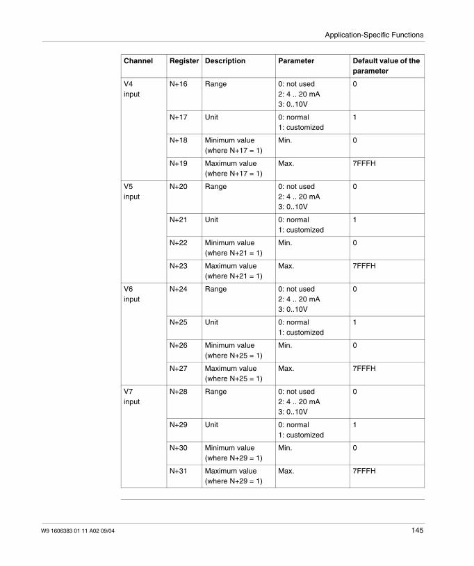
Application-Specific Functions
V4input
N+16 Range 0: not used2: 4 .. 20 mA3: 0..10V
0
N+17 Unit 0: normal1: customized
1
N+18 Minimum value(where N+17 = 1)
Min. 0
N+19 Maximum value(where N+17 = 1)
Max. 7FFFH
V5input
N+20 Range 0: not used2: 4 .. 20 mA3: 0..10V
0
N+21 Unit 0: normal1: customized
1
N+22 Minimum value(where N+21 = 1)
Min. 0
N+23 Maximum value(where N+21 = 1)
Max. 7FFFH
V6input
N+24 Range 0: not used2: 4 .. 20 mA3: 0..10V
0
N+25 Unit 0: normal1: customized
1
N+26 Minimum value(where N+25 = 1)
Min. 0
N+27 Maximum value(where N+25 = 1)
Max. 7FFFH
V7input
N+28 Range 0: not used2: 4 .. 20 mA3: 0..10V
0
N+29 Unit 0: normal1: customized
1
N+30 Minimum value(where N+29 = 1)
Min. 0
N+31 Maximum value(where N+29 = 1)
Max. 7FFFH
Channel Register Description Parameter Default value of theparameter
W9 1606383 01 11 A02 09/04 145
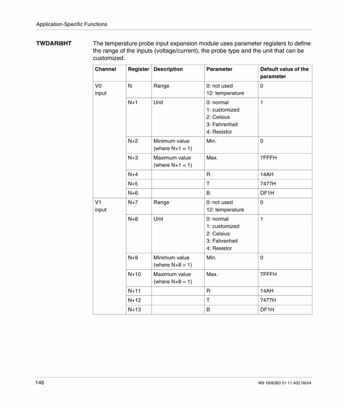
Application-Specific Functions
TWDARI8HT The temperature probe input expansion module uses parameter registers to definethe range of the inputs (voltage/current), the probe type and the unit that can becustomized.
Channel Register Description Parameter Default value of theparameter
V0input
N Range 0: not used12: temperature
0
N+1 Unit 0: normal1: customized2: Celsius3: Fahrenheit4: Resistor
1
N+2 Minimum value(where N+1 = 1)
Min. 0
N+3 Maximum value(where N+1 = 1)
Max. 7FFFH
N+4 R 14AH
N+5 T 7477H
N+6 B DF1H
V1input
N+7 Range 0: not used12: temperature
0
N+8 Unit 0: normal1: customized2: Celsius3: Fahrenheit4: Resistor
1
N+9 Minimum value(where N+8 = 1)
Min. 0
N+10 Maximum value(where N+8 = 1)
Max. 7FFFH
N+11 R 14AH
N+12 T 7477H
N+13 B DF1H
146 W9 1606383 01 11 A02 09/04

Application-Specific Functions
V2input
N+14 Range 0: not used12: temperature
0
N+15 Unit 0: normal1: customized2: Celsius3: Fahrenheit4: Resistor
1
N+16 Minimum value(where N+9 = 1)
Min. 0
N+17 Maximum value(where N+9 = 1)
Max. 7FFFH
N+18 R 14AH
N+19 T 7477H
N+20 B DF1H
V3input
N+21 Range 0: not used12: temperature
0
N+22 Unit 0: normal1: customized2: Celsius3: Fahrenheit4: Resistor
1
N+23 Minimum value(where N+13 = 1)
Min. 0
N+24 Maximum value(where N+13 = 1)
Max. 7FFFH
N+25 R 14AH
N+26 T 7477H
N+27 B DF1H
Channel Register Description Parameter Default value of theparameter
W9 1606383 01 11 A02 09/04 147
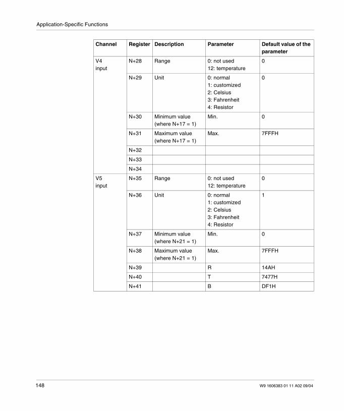
Application-Specific Functions
V4input
N+28 Range 0: not used12: temperature
0
N+29 Unit 0: normal1: customized2: Celsius3: Fahrenheit4: Resistor
0
N+30 Minimum value(where N+17 = 1)
Min. 0
N+31 Maximum value(where N+17 = 1)
Max. 7FFFH
N+32
N+33
N+34
V5input
N+35 Range 0: not used12: temperature
0
N+36 Unit 0: normal1: customized2: Celsius3: Fahrenheit4: Resistor
1
N+37 Minimum value(where N+21 = 1)
Min. 0
N+38 Maximum value(where N+21 = 1)
Max. 7FFFH
N+39 R 14AH
N+40 T 7477H
N+41 B DF1H
Channel Register Description Parameter Default value of theparameter
148 W9 1606383 01 11 A02 09/04
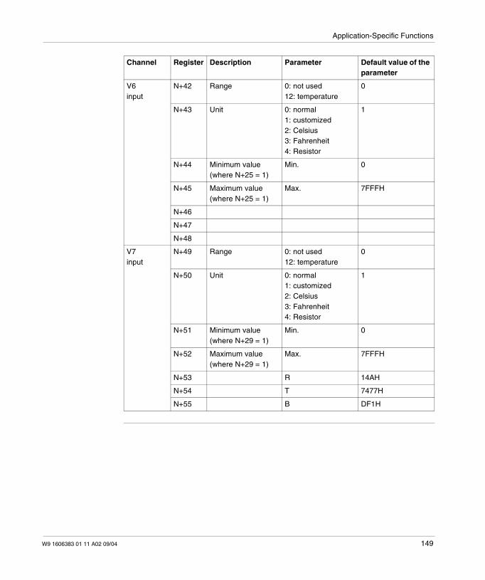
Application-Specific Functions
V6input
N+42 Range 0: not used12: temperature
0
N+43 Unit 0: normal1: customized2: Celsius3: Fahrenheit4: Resistor
1
N+44 Minimum value(where N+25 = 1)
Min. 0
N+45 Maximum value(where N+25 = 1)
Max. 7FFFH
N+46
N+47
N+48
V7input
N+49 Range 0: not used12: temperature
0
N+50 Unit 0: normal1: customized2: Celsius3: Fahrenheit4: Resistor
1
N+51 Minimum value(where N+29 = 1)
Min. 0
N+52 Maximum value(where N+29 = 1)
Max. 7FFFH
N+53 R 14AH
N+54 T 7477H
N+55 B DF1H
Channel Register Description Parameter Default value of theparameter
W9 1606383 01 11 A02 09/04 149
Application-Specific Functions
Specific Functions of the Advantys OTB Modules
Overview The network interface module Advantys OTB features specific I/Os andprogrammable functions.List of built-in functions:
4 fast inputs (40 ms) with programmable filtering,8 inputs (150 ms) with programmable filtering,2 fast Discrete outputs (5 ms),6 relay outputs,2 remote fast counters (5kHz)2 remote very fast counters (20kHz)2 remote pulse generators (PLS or PWM)Possible connection of 7 expansion modules1 communication port
A configuration zone is reserved for each of these functions.
Discrete I/OFiltering
The inputs can be filtered or non filtered. The filtering value is programmable to 3 msor 12 ms.
Remote FastCounter (RFC)
The Advantys OTB network interface module authorizes the use of a maximum of 2fast counters. The function blocks RFC0 and RFC1 are allocated to the inputs I8 andI9 respectively. These inputs can be used as standard discrete inputs if the functionblock is not used.
Remote VeryFast Counter(RVFC)
The Advantys OTB network interface module authorizes the use of a maximum of 2very fast counters. The function blocks RVFC0 and RVFC1 are allocated to theinputs 0 to 3 and 4 to 7 respectively. These inputs can be used as standard discreteinputs if the function block is not used.
Remote PulseGenerators(RPLS or RPWM)
The Advantys OTB network interface module authorizes the use of 2 RPLS orRPWM pulse generators. The function blocks RPLS0/RPWM0 and RPLS1/RPWM1are allocated to the outputs 0 and 1 respectively. These outputs can be used asstandard discrete outputs if the function block is not used.
150 W9 1606383 01 11 A02 09/04

Application-Specific Functions
Associated I/Oand Functions
The I/Os associated with the pulse counters and generators are defined in thefollowing table:
I/O Very fastcounter 0(RVFC0)
Very fastcounter 1(RVFC1)
Fast counter0(RFC0)
Fast counter0(RFC1)
Pulsegenerator 0(RPLS0/RPWM0)
Pulsegenerator 1(RPLS1/RPWM1)
Input 0 X
Input 1 X
Input 2 X
Input 3 X
Input 4 X
Input 5 X
Input 6 X
Input 7 X
Input 8 X
Input 9 X
Output 0 X
Output 1 X
Output 2 X
Output 3 X
Output 4 X
Output 5 X
W9 1606383 01 11 A02 09/04 151
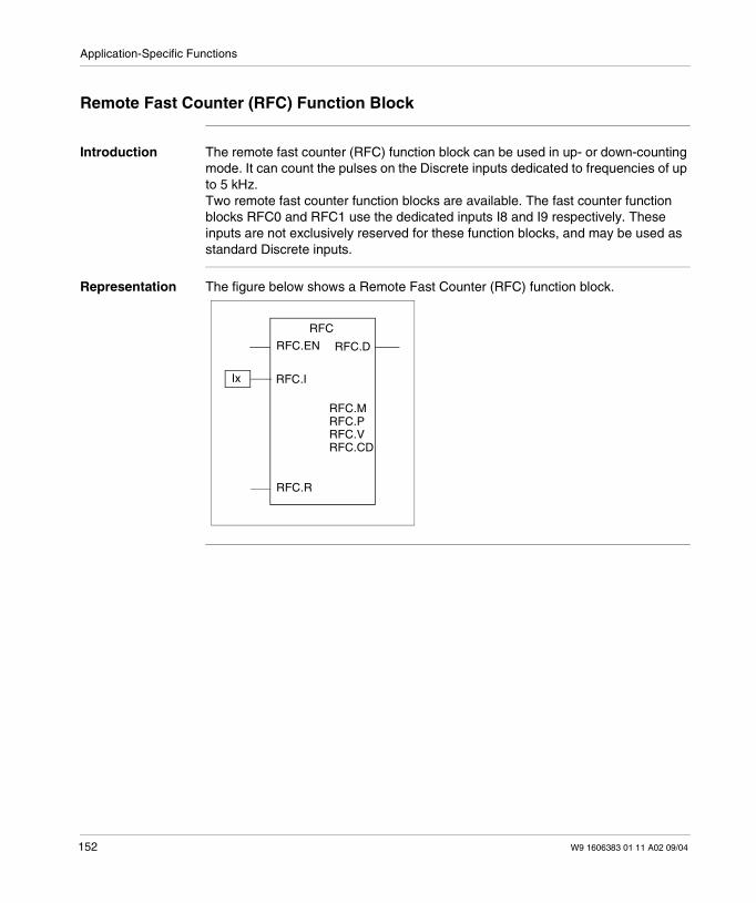
Application-Specific Functions
Remote Fast Counter (RFC) Function Block
Introduction The remote fast counter (RFC) function block can be used in up- or down-countingmode. It can count the pulses on the Discrete inputs dedicated to frequencies of upto 5 kHz.Two remote fast counter function blocks are available. The fast counter functionblocks RFC0 and RFC1 use the dedicated inputs I8 and I9 respectively. Theseinputs are not exclusively reserved for these function blocks, and may be used asstandard Discrete inputs.
Representation The figure below shows a Remote Fast Counter (RFC) function block.
RFC.EN RFC.D
RFC.R
RFC
RFC.M
RFC.I
RFC.PRFC.VRFC.CD
Ix
152 W9 1606383 01 11 A02 09/04
Application-Specific Functions
Parameters The following table shows the parameters for the Remote Fast Counter functionblock.
Operation When the RFC function block is configured to up-count, the current value isincremented by one when a rising edge appears at the dedicated input. When thepreset value RFC.P is reached, the Done output bit RFC.D is set to 1 and the currentvalue RFC.V is set to zero.If the RFC function block is configured to down-count, the current value is decreasedby one when a rising edge appears at the dedicated input. When the value is zero,the Done output bit RFC.D is set to 1 and the current value RFC.P is set to the presetvalue.
Parameter Description Description
RFC.M Counting mode Parameter used to select between:not used,counter,Down Counter
RFC.P Preset value Value to trigger the RFC.D Done bit and reset the RFC.Vcurrent value.
RFC.V Current Value The current value increments or decrements according thecounting mode selected. This value is between zero andthe RFC.P preset value.
RFC.EN Enter to enable Validation of the RFC block operation. When set to 0, theblock is inhibited and the current value is unchanged.
RFC.R Reset Used to initialize the block. When set to 1, the current valueis set to:
0 if the block is configured in counting mode,RFC.P if the block is configured in downcounting mode.
RFC.D done Done switches to 1 if:RFC.V reaches RFC.P in upcounting mode,RFC.V reaches zero in downcounting mode.
RFC.CD Reset Done When set to 1, this bit is used to reset the RFC.D bit. Thisbit is processed depending on its level; if the user does notreset it to 0, the RFC.D bit is never reactivated.
RFC.I Physical input Input dedicated to up/down counting:I8 for the RFC0 fast counter,I9 for the RFC1. fast counter,
W9 1606383 01 11 A02 09/04 153

Application-Specific Functions
Notes The function block will only be activated after the RFC.R function block is initializedand the RFC.EN input enabled.The selection or modification of the RFC.M counting mode will only be taken intoaccount on activation of the RFC.R command.
Fallback ModesRFC.EM
When the PLC stops or detects a communication error, the RFC function block mayoperate differently according to the programmed fallback mode.The programmable fallback modes of the RFC function block are as follows:
counter reset (equivalent of setting the RFC.R to 1),set the current value of the RFC function block counter (equivalent of settingRFC.EN to 0),continue counting.
154 W9 1606383 01 11 A02 09/04
Application-Specific Functions
Fast Counter (RFC) Parameter Registers
At a Glance The fast counters (RFC0 and RFC1) use the configuration parameters of thesupported functions.
Registers 600 to627
Specific function of fast counter 0 (RFC0).
Specific function of fast counter 1 (RFC1).
Registers Parameter Description Access
600601
RFC.V Current Value read
Current Value
602 RFC.D Bit [0]: D (Done) read
603 RFC.M Counting mode:0: not used1: counter2: downcounter
read/write
604 RFC.EM Fallback mode:0: reset to zero of the counter1: stop counting, save the last value read andfreeze counter2: continue counting
read/write
605606
RFC.P Preset value read/write
Preset value
607 RFC.ENRFC.RRFC.CD
Bit [0]: validation of the input ENBit [1]: R (Reset)Bit [2]: reset of the RFC.D bit
read/write
Registers Description Access Access
620...627 Description identical to that for counter 0
W9 1606383 01 11 A02 09/04 155
Application-Specific Functions
Remote Very Fast Counter (RVFC) Function Block
Introduction The Remote Very Fast Counter (RVFC) function block can be configured to performany one of the following functions:
Up/down counterUp/down 2-phase counterSingle Up CounterSingle Down CounterFrequency Meter
Two very fast counters are available. The RVFC function block supports counting ofDiscrete inputs up to frequencies of 20 kHz. The very fast counter function blocksRVFC0 and RVFC1 respectively use the I/Os dedicated to these functions.A Remote Very Fast Counter (RVFC) operates at a maximum frequency of 20 kHz,and for a value range between 0 and 4 294 967 295.
Notes The function block will only be activated after the RVFC.R function block is initializedand the RVFC.EN input enabled.The selection or modification of the RVFC.M counting mode will only be taken intoaccount on activation of the RVFC.R command.
156 W9 1606383 01 11 A02 09/04

Application-Specific Functions
Dedicated I/OAssignments
The Remote Very Fast Counter (RVFC) function blocks use dedicated inputs andoutputs. These inputs and outputs are not exclusively reserved for these functionblocks, and may be used as Discrete I/Os.The following array summarizes the possible assignments:
Main inputs Auxiliary inputs Reflex outputs
RVFC0 Operating mode IA input IB input IPres Ica Output 0 Output 1
Up/down counter I1pulse
I00=UP/1=DO
I2 (1) I3 (1) Q2 (1) Q3 (1)
Up/down 2-phasecounter
I1Phase A
I0Phase B
I2 (1) I3 (1) Q2 (1) Q3 (1)
Single Up Counter I1 Not used I2 (1) I3 (1) Q2 (1) Q3 (1)
Single Down Counter I1 Not used I2 (1) I3 (1) Q2 (1) Q3 (1)
Frequency Meter I1 Not used Not used Not used Not used Not used
RVFC1 Selected Use IA input Input IB) IPres Ica Output 0 Output 1
Up/down counter I7Pulse
I60=UP/1=DO
I5 (1) I4 (1) Q4 (1) Q5 (1)
Up/Down 2-PhaseCounter
I7Phase A
I6Phase B
I5 (1) I4 (1) Q4 (1) Q5 (1)
Single Up Counter I7 Not used I5 (1) I4 (1) Q4 (1) Q5 (1)
Single Down Counter I7 Not used I5 (1) I4 (1) Q4 (1) Q5 (1)
Frequency Meter I7 Not used Not used Not used Not used Not used
Key:(1) = optionalInput IA = pulse inputInput IB = pulses or UP/DOUP/DO = Up / Down countingIpres = preset inputIca = catch inputWhen not used by the function, the input or output remains a Discrete I/O.
W9 1606383 01 11 A02 09/04 157
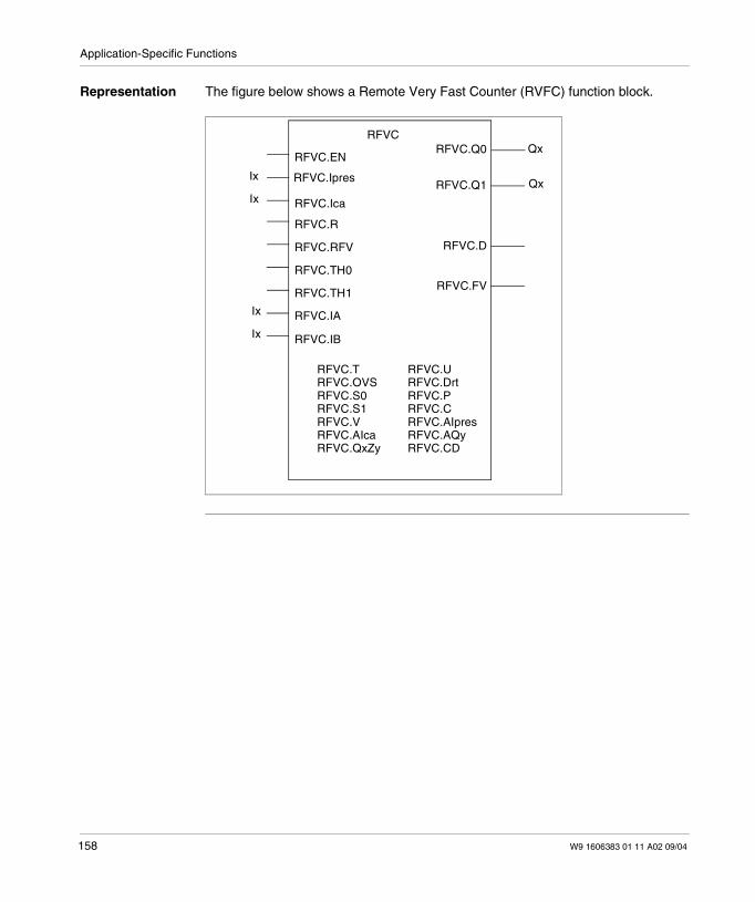
Application-Specific Functions
Representation The figure below shows a Remote Very Fast Counter (RVFC) function block.
RFVC.EN
RFVC.Ipres
RFVC.Ica
RFVC.R
RFVC.RFV
RFVC.TH0
RFVC.TH1
RFVC.IA
RFVC.IB
RFVC
RFVC.Q1
RFVC.D
RFVC.FV
RFVC.TRFVC.OVSRFVC.S0RFVC.S1RFVC.VRFVC.AIcaRFVC.QxZy
RFVC.URFVC.DrtRFVC.PRFVC.CRFVC.AIpresRFVC.AQyRFVC.CD
RFVC.Q0
Ix
Ix
Ix
Ix
Qx
Qx
158 W9 1606383 01 11 A02 09/04
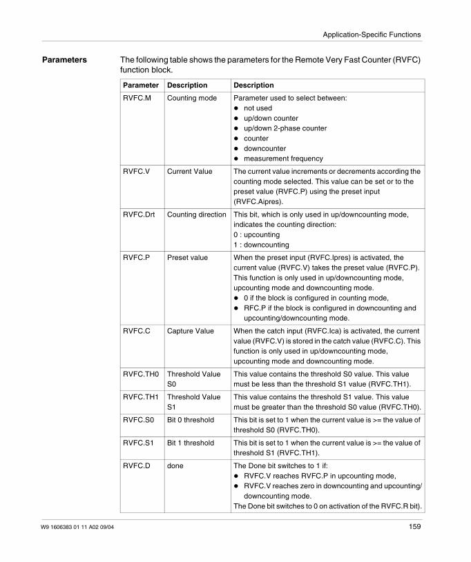
Application-Specific Functions
Parameters The following table shows the parameters for the Remote Very Fast Counter (RVFC)function block.
Parameter Description Description
RVFC.M Counting mode Parameter used to select between:not usedup/down counterup/down 2-phase countercounterdowncountermeasurement frequency
RVFC.V Current Value The current value increments or decrements according thecounting mode selected. This value can be set or to thepreset value (RVFC.P) using the preset input(RVFC.Aipres).
RVFC.Drt Counting direction This bit, which is only used in up/downcounting mode,indicates the counting direction:0 : upcounting1 : downcounting
RVFC.P Preset value When the preset input (RVFC.Ipres) is activated, thecurrent value (RVFC.V) takes the preset value (RVFC.P).This function is only used in up/downcounting mode,upcounting mode and downcounting mode.
0 if the block is configured in counting mode,RFC.P if the block is configured in downcounting andupcounting/downcounting mode.
RVFC.C Capture Value When the catch input (RVFC.Ica) is activated, the currentvalue (RVFC.V) is stored in the catch value (RVFC.C). Thisfunction is only used in up/downcounting mode,upcounting mode and downcounting mode.
RVFC.TH0 Threshold ValueS0
This value contains the threshold S0 value. This valuemust be less than the threshold S1 value (RVFC.TH1).
RVFC.TH1 Threshold ValueS1
This value contains the threshold S1 value. This valuemust be greater than the threshold S0 value (RVFC.TH0).
RVFC.S0 Bit 0 threshold This bit is set to 1 when the current value is >= the value ofthreshold S0 (RVFC.TH0).
RVFC.S1 Bit 1 threshold This bit is set to 1 when the current value is >= the value ofthreshold S1 (RVFC.TH1).
RVFC.D done The Done bit switches to 1 if:RVFC.V reaches RVFC.P in upcounting mode,RVFC.V reaches zero in downcounting and upcounting/downcounting mode.
The Done bit switches to 0 on activation of the RVFC.R bit).
W9 1606383 01 11 A02 09/04 159
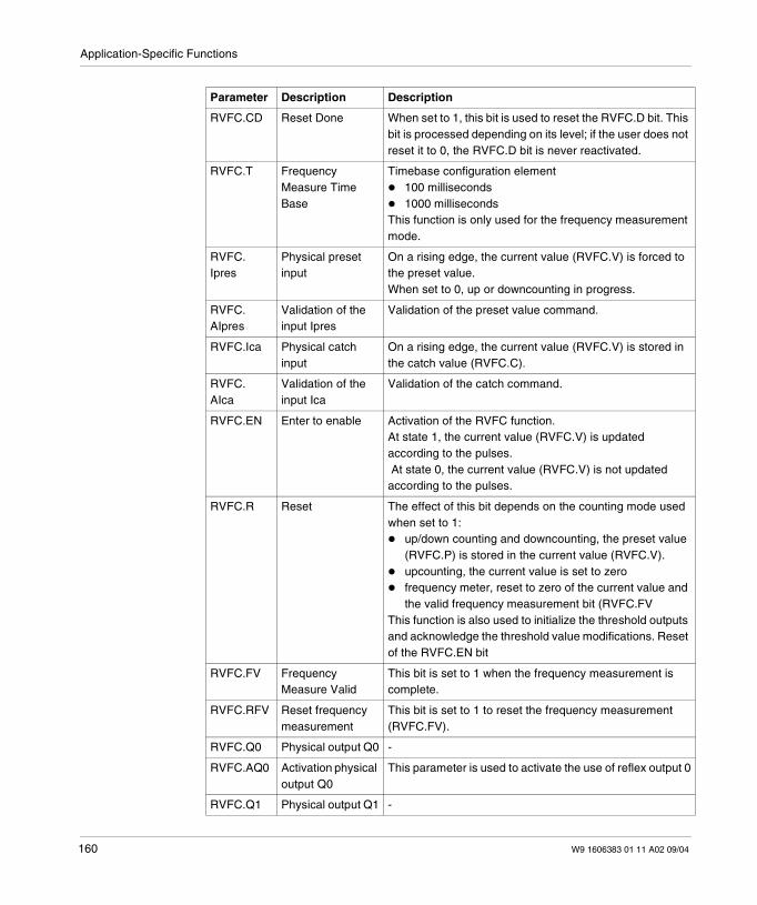
Application-Specific Functions
RVFC.CD Reset Done When set to 1, this bit is used to reset the RVFC.D bit. Thisbit is processed depending on its level; if the user does notreset it to 0, the RVFC.D bit is never reactivated.
RVFC.T FrequencyMeasure TimeBase
Timebase configuration element100 milliseconds1000 milliseconds
This function is only used for the frequency measurementmode.
RVFC.Ipres
Physical presetinput
On a rising edge, the current value (RVFC.V) is forced tothe preset value.When set to 0, up or downcounting in progress.
RVFC.AIpres
Validation of theinput Ipres
Validation of the preset value command.
RVFC.Ica Physical catchinput
On a rising edge, the current value (RVFC.V) is stored inthe catch value (RVFC.C).
RVFC.AIca
Validation of theinput Ica
Validation of the catch command.
RVFC.EN Enter to enable Activation of the RVFC function.At state 1, the current value (RVFC.V) is updatedaccording to the pulses.At state 0, the current value (RVFC.V) is not updated
according to the pulses.
RVFC.R Reset The effect of this bit depends on the counting mode usedwhen set to 1:
up/down counting and downcounting, the preset value(RVFC.P) is stored in the current value (RVFC.V).upcounting, the current value is set to zerofrequency meter, reset to zero of the current value andthe valid frequency measurement bit (RVFC.FV
This function is also used to initialize the threshold outputsand acknowledge the threshold value modifications. Resetof the RVFC.EN bit
RVFC.FV FrequencyMeasure Valid
This bit is set to 1 when the frequency measurement iscomplete.
RVFC.RFV Reset frequencymeasurement
This bit is set to 1 to reset the frequency measurement(RVFC.FV).
RVFC.Q0 Physical output Q0 -
RVFC.AQ0 Activation physicaloutput Q0
This parameter is used to activate the use of reflex output 0
RVFC.Q1 Physical output Q1 -
Parameter Description Description
160 W9 1606383 01 11 A02 09/04
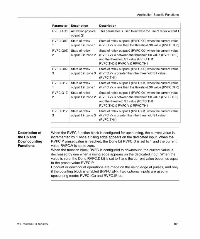
Application-Specific Functions
Description ofthe Up andDowncountingFunctions
When the RVFC function block is configured for upcounting, the current value isincremented by 1 once a rising edge appears on the dedicated input. When theRVFC.P preset value is reached, the Done bit RVFC.D is set to 1 and the currentvalue RVFC.V is set to zero.When the function block RVFC is configured to downcount, the current value isdecreased by one when a rising edge appears on the dedicated input. When thevalue is zero, the Done RVFC.D bit is set to 1 and the current value becomes equalto the preset value RVFC.P.Upcount or downcount operations are made on the rising edge of pulses, and onlyif the counting block is enabled (RVFC.EN). Two optional inputs are used inupcounting mode: RVFC.ICa and RVFC.IPres.
RVFC.AQ1 Activation physicaloutput Q1
This parameter is used to activate the use of reflex output 1
RVFC.Q0Z1
State of reflexoutput 0 in zone 1
State of reflex output 0 (RVFC.Q0) when the current value(RVFC.V) is less than the threshold S0 value (RVFC.TH0)
RVFC.Q0Z2
State of reflexoutput 0 in zone 2
State of reflex output 0 (RVFC.Q0) when the current value(RVFC.V) is between the threshold S0 value (RVFC.TH0)and the threshold S1 value (RVFC.TH1)RVFC.TH0 £ RVFC.V £ RFVC.TH1
RVFC.Q0Z3
State of reflexoutput 0 in zone 3
State of reflex output 0 (RVFC.Q0) when the current value(RVFC.V) is greater than the threshold S1 value(RVFC.TH1)
RVFC.Q1Z1
State of reflexoutput 1 in zone 1
State of reflex output 1 (RVFC.Q1) when the current value(RVFC.V) is less than the threshold S0 value (RVFC.TH0)
RVFC.Q1Z2
State of reflexoutput 1 in zone 2
State of reflex output 1 (RVFC.Q1) when the current value(RVFC.V) is between the threshold S0 value (RVFC.TH0)and the threshold S1 value (RVFC.TH1)RVFC.TH0 £ RVFC.V £ RFVC.TH1
RVFC.Q1Z3
State of reflexoutput 1 in zone 3
State of reflex output 1 (RVFC.Q1) when the current value(RVFC.V) is greater than the threshold S1 value(RVFC.TH1)
Parameter Description Description
W9 1606383 01 11 A02 09/04 161

Application-Specific Functions
Notes onFunction BlockOutputs
The current value is compared with two threshold values (RVFC.TH0 andRVFC.TH1). The states of both threshold bits (RVFC.S0 and RVFC.S1) depend onthe results of this comparison. State 1 if the current value is greater than or equal tothe threshold value and 0 if the current value is less than the threshold value. Reflexoutputs (if configured) are activated in accordance with these comparisons. It ispossible to configure zero, one or two reflex outputs.
Note: Not applicable to the frequency meter counting mode
162 W9 1606383 01 11 A02 09/04
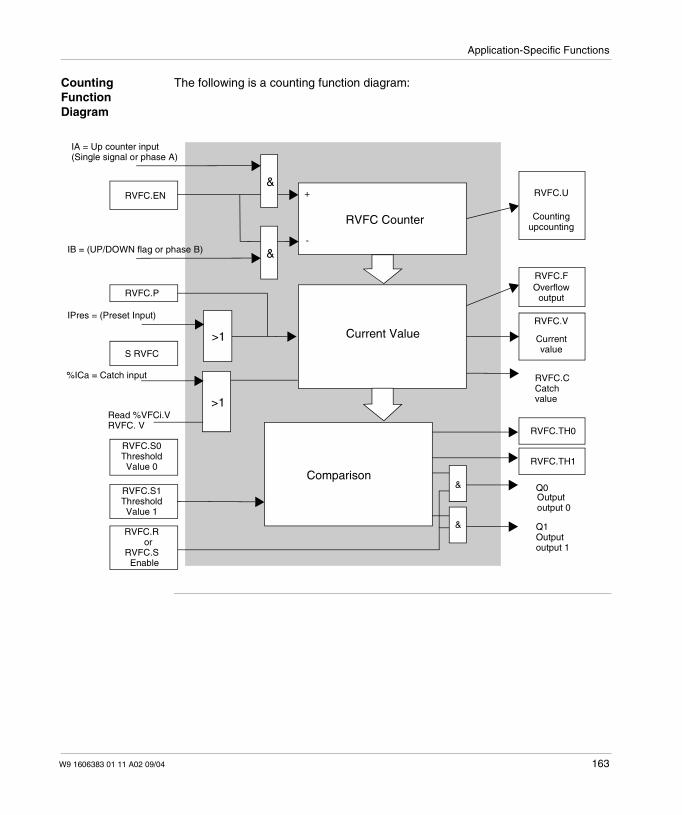
Application-Specific Functions
CountingFunctionDiagram
The following is a counting function diagram:
&
&
>1
>1
RVFC Counter
Current Value
Comparison
RVFC.U
Countingupcounting
RVFC.FOverflow
output
RVFC.V
Currentvalue
RVFC.TH0
RVFC.TH1
RVFC.CCatchvalue
Q0Outputoutput 0
Q1Outputoutput 1
&
&
+
-
IA = Up counter input(Single signal or phase A)
RVFC.EN
RVFC.P
IB = (UP/DOWN flag or phase B)
S RVFC
RVFC.S0ThresholdValue 0
RVFC.S1ThresholdValue 1
RVFC.Ror
RVFC.SEnable
IPres = (Preset Input)
%ICa = Catch input
Read %VFCi.VRVFC. V
Current Value
W9 1606383 01 11 A02 09/04 163
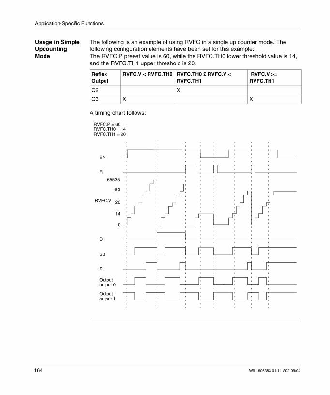
Application-Specific Functions
Usage in SimpleUpcountingMode
The following is an example of using RVFC in a single up counter mode. Thefollowing configuration elements have been set for this example:The RVFC.P preset value is 60, while the RVFC.TH0 lower threshold value is 14,and the RVFC.TH1 upper threshold is 20.
A timing chart follows:
ReflexOutput
RVFC.V < RVFC.TH0 RVFC.TH0 £ RVFC.V <RVFC.TH1
RVFC.V >=RVFC.TH1
Q2 X
Q3 X X
RVFC.P = 60RVFC.TH0 = 14RVFC.TH1 = 20
RVFC.V
EN
R
65535
20
14
D
S0
Outputoutput 0
S1
Outputoutput 1
60
0
164 W9 1606383 01 11 A02 09/04
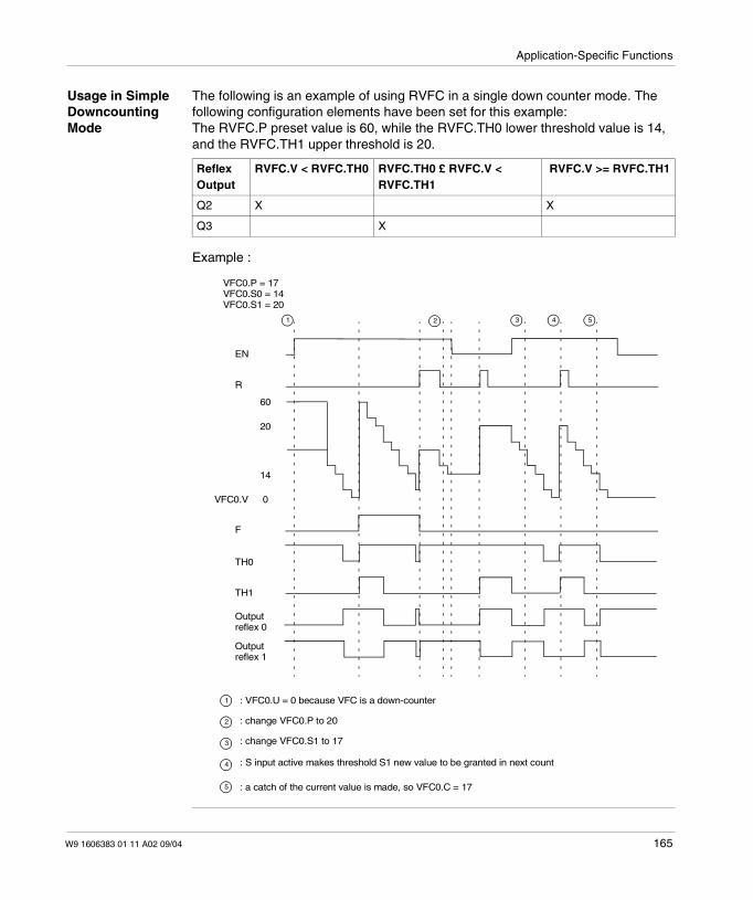
Application-Specific Functions
Usage in SimpleDowncountingMode
The following is an example of using RVFC in a single down counter mode. Thefollowing configuration elements have been set for this example:The RVFC.P preset value is 60, while the RVFC.TH0 lower threshold value is 14,and the RVFC.TH1 upper threshold is 20.
Example :
ReflexOutput
RVFC.V < RVFC.TH0 RVFC.TH0 £ RVFC.V <RVFC.TH1
RVFC.V >= RVFC.TH1
Q2 X X
Q3 X
VFC0.P = 17VFC0.S0 = 14VFC0.S1 = 20
EN
R
60
20
14
0VFC0.V
F
TH0
Outputreflex 0
TH1
Outputreflex 1
1 3 4 5
: VFC0.U = 0 because VFC is a down-counter
: change VFC0.S1 to 17
: S input active makes threshold S1 new value to be granted in next count
1
2
3
4
2
5 : a catch of the current value is made, so VFC0.C = 17
: change VFC0.P to 20
W9 1606383 01 11 A02 09/04 165
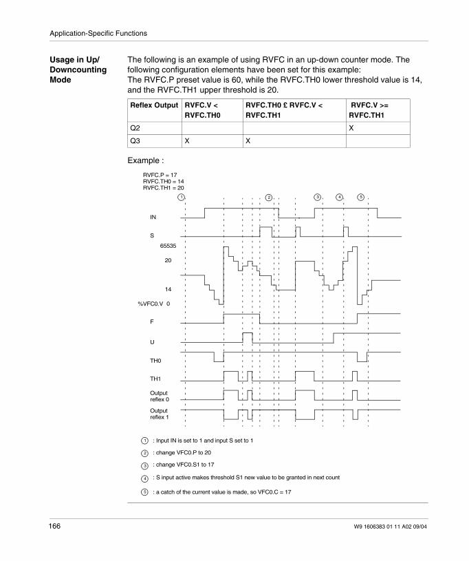
Application-Specific Functions
Usage in Up/DowncountingMode
The following is an example of using RVFC in an up-down counter mode. Thefollowing configuration elements have been set for this example:The RVFC.P preset value is 60, while the RVFC.TH0 lower threshold value is 14,and the RVFC.TH1 upper threshold is 20.
Example :
Reflex Output RVFC.V <RVFC.TH0
RVFC.TH0 £ RVFC.V <RVFC.TH1
RVFC.V >=RVFC.TH1
Q2 X
Q3 X X
RVFC.P = 17RVFC.TH0 = 14RVFC.TH1 = 20
IN
S
65535
20
14
0%VFC0.V
F
TH0
Outputreflex 0
TH1
Outputreflex 1
1 3 4 5
: Input IN is set to 1 and input S set to 1
: change VFC0.S1 to 17
: S input active makes threshold S1 new value to be granted in next count
1
2
3
4
2
5 : a catch of the current value is made, so VFC0.C = 17
: change VFC0.P to 20
U
166 W9 1606383 01 11 A02 09/04
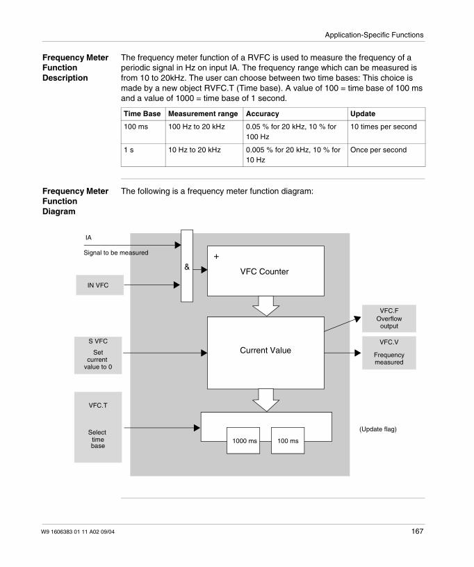
Application-Specific Functions
Frequency MeterFunctionDescription
The frequency meter function of a RVFC is used to measure the frequency of aperiodic signal in Hz on input IA. The frequency range which can be measured isfrom 10 to 20kHz. The user can choose between two time bases: This choice ismade by a new object RVFC.T (Time base). A value of 100 = time base of 100 msand a value of 1000 = time base of 1 second.
Frequency MeterFunctionDiagram
The following is a frequency meter function diagram:
Time Base Measurement range Accuracy Update
100 ms 100 Hz to 20 kHz 0.05 % for 20 kHz, 10 % for100 Hz
10 times per second
1 s 10 Hz to 20 kHz 0.005 % for 20 kHz, 10 % for10 Hz
Once per second
& VFC Counter
current value
VFC.FOverflow
output
VFC.V
Frequency
+
IN VFC
S VFC
Current Valuemeasured
(Update flag)
1000 ms 100 ms
Setcurrent
VFC.T
Select
base
IA
Signal to be measured
value to 0
time
W9 1606383 01 11 A02 09/04 167
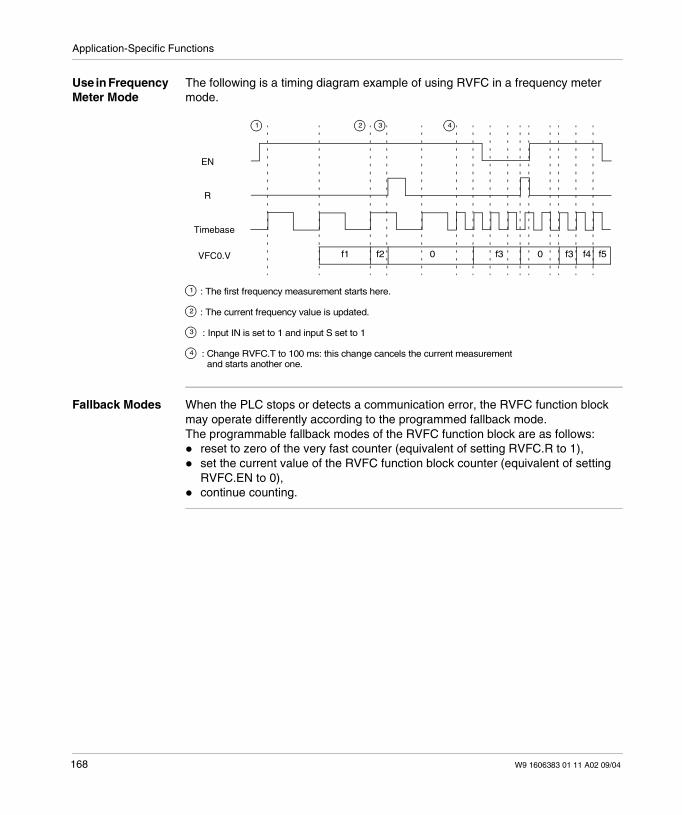
Application-Specific Functions
Use in FrequencyMeter Mode
The following is a timing diagram example of using RVFC in a frequency metermode.
Fallback Modes When the PLC stops or detects a communication error, the RVFC function blockmay operate differently according to the programmed fallback mode.The programmable fallback modes of the RVFC function block are as follows:
reset to zero of the very fast counter (equivalent of setting RVFC.R to 1),set the current value of the RVFC function block counter (equivalent of settingRVFC.EN to 0),continue counting.
EN
R
Timebase
VFC0.V
1 2 3 4
f1 f2 0 f3 f4 f5f30
1
2
: The first frequency measurement starts here.
: The current frequency value is updated.
: Input IN is set to 1 and input S set to 1
: Change RVFC.T to 100 ms: this change cancels the current measurement
3
4
and starts another one.
168 W9 1606383 01 11 A02 09/04
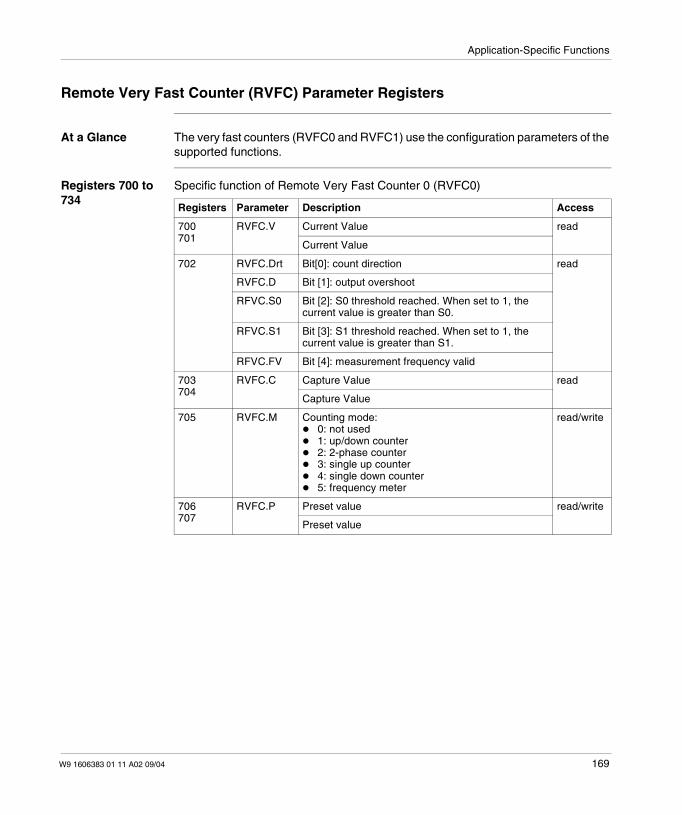
Application-Specific Functions
Remote Very Fast Counter (RVFC) Parameter Registers
At a Glance The very fast counters (RVFC0 and RVFC1) use the configuration parameters of thesupported functions.
Registers 700 to734
Specific function of Remote Very Fast Counter 0 (RVFC0)
Registers Parameter Description Access
700701
RVFC.V Current Value read
Current Value
702 RVFC.Drt Bit[0]: count direction read
RVFC.D Bit [1]: output overshoot
RFVC.S0 Bit [2]: S0 threshold reached. When set to 1, thecurrent value is greater than S0.
RFVC.S1 Bit [3]: S1 threshold reached. When set to 1, thecurrent value is greater than S1.
RFVC.FV Bit [4]: measurement frequency valid
703704
RVFC.C Capture Value read
Capture Value
705 RVFC.M Counting mode:0: not used1: up/down counter2: 2-phase counter3: single up counter4: single down counter5: frequency meter
read/write
706707
RVFC.P Preset value read/write
Preset value
W9 1606383 01 11 A02 09/04 169
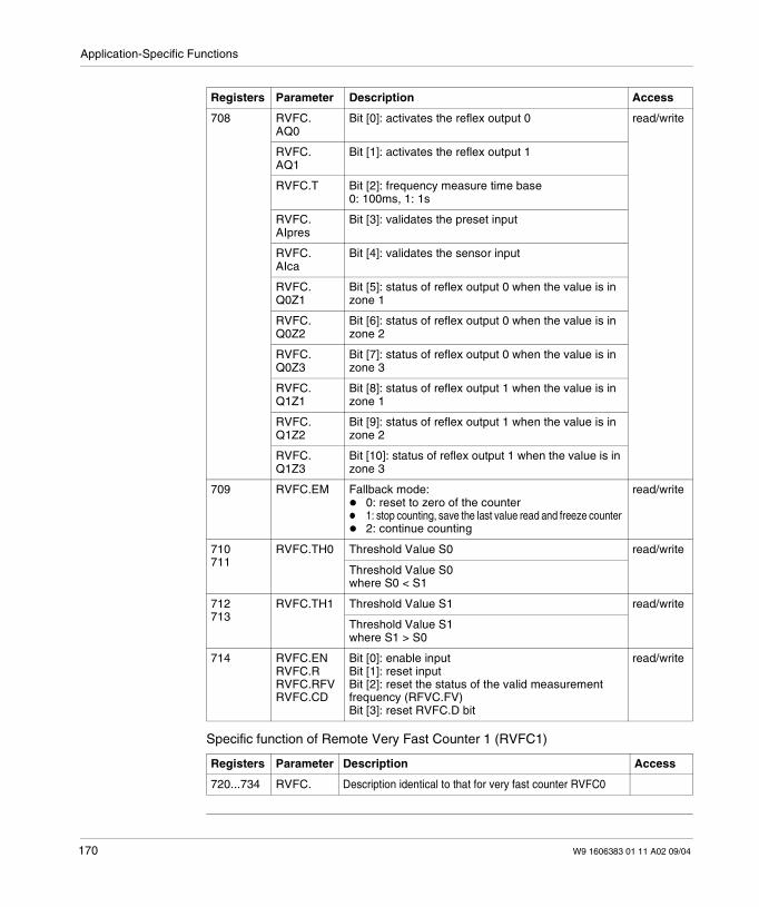
Application-Specific Functions
Specific function of Remote Very Fast Counter 1 (RVFC1)
708 RVFC.AQ0
Bit [0]: activates the reflex output 0 read/write
RVFC.AQ1
Bit [1]: activates the reflex output 1
RVFC.T Bit [2]: frequency measure time base0: 100ms, 1: 1s
RVFC.AIpres
Bit [3]: validates the preset input
RVFC.AIca
Bit [4]: validates the sensor input
RVFC.Q0Z1
Bit [5]: status of reflex output 0 when the value is inzone 1
RVFC.Q0Z2
Bit [6]: status of reflex output 0 when the value is inzone 2
RVFC.Q0Z3
Bit [7]: status of reflex output 0 when the value is inzone 3
RVFC.Q1Z1
Bit [8]: status of reflex output 1 when the value is inzone 1
RVFC.Q1Z2
Bit [9]: status of reflex output 1 when the value is inzone 2
RVFC.Q1Z3
Bit [10]: status of reflex output 1 when the value is inzone 3
709 RVFC.EM Fallback mode:0: reset to zero of the counter1: stop counting, save the last value read and freeze counter2: continue counting
read/write
710711
RVFC.TH0 Threshold Value S0 read/write
Threshold Value S0where S0 < S1
712713
RVFC.TH1 Threshold Value S1 read/write
Threshold Value S1where S1 > S0
714 RVFC.ENRVFC.RRVFC.RFVRVFC.CD
Bit [0]: enable inputBit [1]: reset inputBit [2]: reset the status of the valid measurementfrequency (RFVC.FV)Bit [3]: reset RVFC.D bit
read/write
Registers Parameter Description Access
720...734 RVFC. Description identical to that for very fast counter RVFC0
Registers Parameter Description Access
170 W9 1606383 01 11 A02 09/04
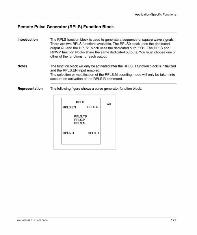
Application-Specific Functions
Remote Pulse Generator (RPLS) Function Block
Introduction The RPLS function block is used to generate a sequence of square wave signals.There are two RPLS functions available. The RPLS0 block uses the dedicatedoutput Q0 and the RPLS1 block uses the dedicated output Q1. The RPLS andRPWM function blocks share the same dedicated outputs. You must choose one orother of the functions for each output.
Notes The function block will only be activated after the RPLS.R function block is initializedand the RPLS.EN input enabled.The selection or modification of the RPLS.M counting mode will only be taken intoaccount on activation of the RPLS.R command.
Representation The following figure shows a pulse generator function block:
RPLS.EN RPLS.Q
RPLS.R
RPLS
RPLS.TB
RPLS.D
RPLS.PRPLS.N
Qx
W9 1606383 01 11 A02 09/04 171
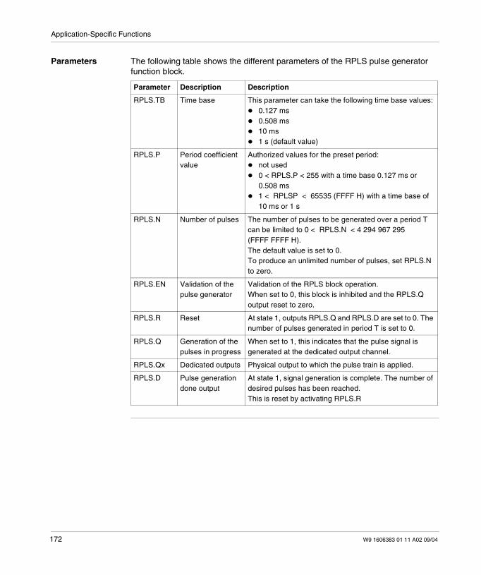
Application-Specific Functions
Parameters The following table shows the different parameters of the RPLS pulse generatorfunction block.
Parameter Description Description
RPLS.TB Time base This parameter can take the following time base values:0.127 ms0.508 ms10 ms1 s (default value)
RPLS.P Period coefficientvalue
Authorized values for the preset period:not used0 < RPLS.P < 255 with a time base 0.127 ms or0.508 ms1 < RPLSP < 65535 (FFFF H) with a time base of10 ms or 1 s
RPLS.N Number of pulses The number of pulses to be generated over a period Tcan be limited to 0 < RPLS.N < 4 294 967 295(FFFF FFFF H).The default value is set to 0.To produce an unlimited number of pulses, set RPLS.Nto zero.
RPLS.EN Validation of thepulse generator
Validation of the RPLS block operation.When set to 0, this block is inhibited and the RPLS.Qoutput reset to zero.
RPLS.R Reset At state 1, outputs RPLS.Q and RPLS.D are set to 0. Thenumber of pulses generated in period T is set to 0.
RPLS.Q Generation of thepulses in progress
When set to 1, this indicates that the pulse signal isgenerated at the dedicated output channel.
RPLS.Qx Dedicated outputs Physical output to which the pulse train is applied.
RPLS.D Pulse generationdone output
At state 1, signal generation is complete. The number ofdesired pulses has been reached.This is reset by activating RPLS.R
172 W9 1606383 01 11 A02 09/04
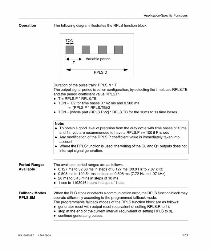
Application-Specific Functions
Operation The following diagram illustrates the RPLS function block:
Duration of the pulse train: RPLS.N * TThe output signal period is set on configuration, by selecting the time base RPLS.TBand the period coefficient value RPLS.P.
T = RPLS.P * RPLS.TBTON = T/2 for time bases 0.142 ms and 0.508 ms
= (RPLS.P * RPLS.TB)/2TON = [whole part (RPLS.P)/2] * RPLS.TB for the 10ms to 1s time bases.
Period RangesAvailable
The available period ranges are as follows:0.127 ms to 32.38 ms in steps of 0.127 ms (30.9 Hz to 7.87 kHz)0.508 ms to 129.54 ms in steps of 0.508 ms (7.72 Hz to 1.97 kHz)20 ms to 5.45 mins in steps of 10 ms1 sec to 1193046 hours in steps of 1 sec
Fallback ModesRPLS.EM
When the PLC stops or detects a communication error, the RPLS function block mayoperate differently according to the programmed fallback mode.The programmable fallback modes of the RPLS function block are as follows:
generator reset with output reset (equivalent of setting RPLS.R to 1).stop at the end of the current interval (equivalent of setting RPLS to 0),continue generating pulses.
Note:To obtain a good level of precision from the duty cycle with time bases of 10msand 1s, you are recommended to have a RPLS.P >= 100 if P is odd.Any modification of the RPLS.P coefficient value is immediately taken intoaccount.Where the RPLS function is used, the writing of the Q0 and Q1 outputs does notinterrupt signal generation.
Variable periodT
TON
RPLS.D
W9 1606383 01 11 A02 09/04 173

Application-Specific Functions
Pulse GeneratorExample
The following is an illustration of a pulse diagram of the RPLS function block.
Input RPLS.EN
Number of pulses
Dedicated output Qx
RPLS.Q
RPLS.D
RPLS.N
174 W9 1606383 01 11 A02 09/04
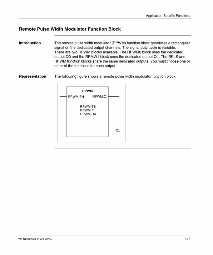
Application-Specific Functions
Remote Pulse Width Modulator Function Block
Introduction The remote pulse width modulator (RPWM) function block generates a rectangularsignal on the dedicated output channels. The signal duty cycle is variable.There are two RPWM blocks available. The RPWM0 block uses the dedicatedoutput Q0 and the RPMW1 block uses the dedicated output Q1. The RPLS andRPWM function blocks share the same dedicated outputs. You must choose one orother of the functions for each output.
Representation The following figure shows a remote pulse width modulator function block:
RPWM.EN RPWM.Q
RPWM
RPWM.TBRPWM.PRPWM.RA
Qx
W9 1606383 01 11 A02 09/04 175
Application-Specific Functions
Parameters The following table shows the different parameters of the remote pulse widthmodulator (RPWM) function block.
Parameter Description Description
RPWM.TB Time base This parameter can take the following time base values:0.127 ms0.508 ms10 ms1 s (default value)
RPWM.P Period coefficientvalue
Authorized values for the preset period:not used0 < RPWM.P < 255 with a time base 0.127 ms or0.508 ms1 < RPWM.P < 65535 (FFFF H) with a time base of10 ms or 1 s
RPWM.RA Duty cycle This value sets the percentage (0% < R < 100%) of thesignal in state 1 in a period T.The default value is 0 (values greater than 100 areconsidered to be equal to 100).
RPWM.EN Validation of thepulse generator
Validation of the RPWM block operation.When set to 0, this block is inhibited and the RPLS.Qoutput reset to zero.
RPLS.Q Generation of thepulses inprogress
When set to 1, this indicates that the pulse signal isgenerated at the dedicated output channel.
RPWM.Qx Dedicatedoutputs
Physical output to which the pulse train is applied.
176 W9 1606383 01 11 A02 09/04
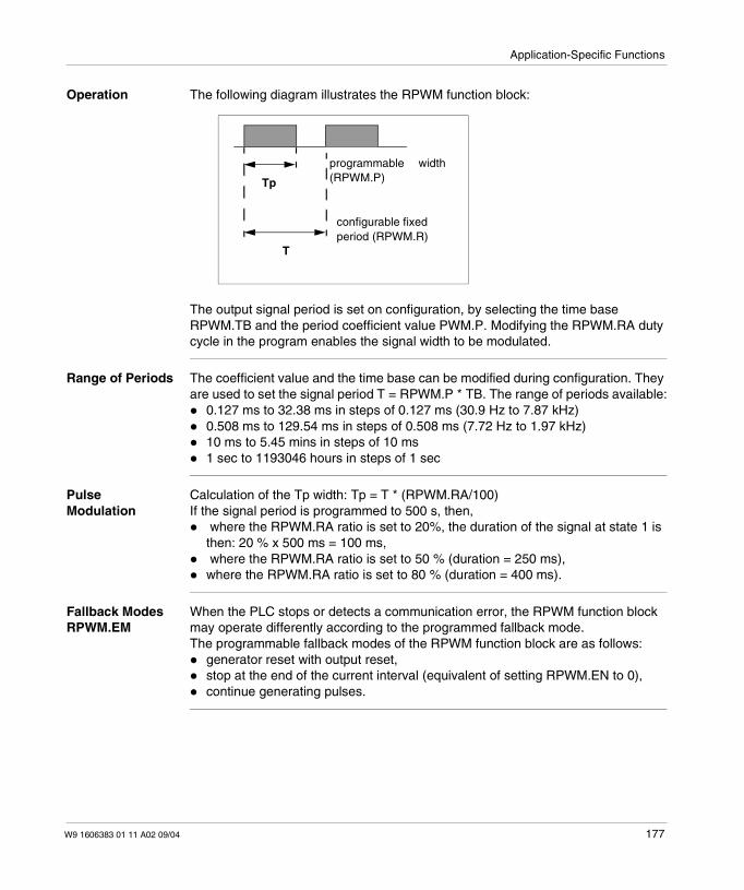
Application-Specific Functions
Operation The following diagram illustrates the RPWM function block:
The output signal period is set on configuration, by selecting the time baseRPWM.TB and the period coefficient value PWM.P. Modifying the RPWM.RA dutycycle in the program enables the signal width to be modulated.
Range of Periods The coefficient value and the time base can be modified during configuration. Theyare used to set the signal period T = RPWM.P * TB. The range of periods available:
0.127 ms to 32.38 ms in steps of 0.127 ms (30.9 Hz to 7.87 kHz)0.508 ms to 129.54 ms in steps of 0.508 ms (7.72 Hz to 1.97 kHz)10 ms to 5.45 mins in steps of 10 ms1 sec to 1193046 hours in steps of 1 sec
PulseModulation
Calculation of the Tp width: Tp = T * (RPWM.RA/100)If the signal period is programmed to 500 s, then,
where the RPWM.RA ratio is set to 20%, the duration of the signal at state 1 isthen: 20 % x 500 ms = 100 ms,where the RPWM.RA ratio is set to 50 % (duration = 250 ms),
where the RPWM.RA ratio is set to 80 % (duration = 400 ms).
Fallback ModesRPWM.EM
When the PLC stops or detects a communication error, the RPWM function blockmay operate differently according to the programmed fallback mode.The programmable fallback modes of the RPWM function block are as follows:
generator reset with output reset,stop at the end of the current interval (equivalent of setting RPWM.EN to 0),continue generating pulses.
Tp
programmable width(RPWM.P)
configurable fixedperiod (RPWM.R)
T
W9 1606383 01 11 A02 09/04 177
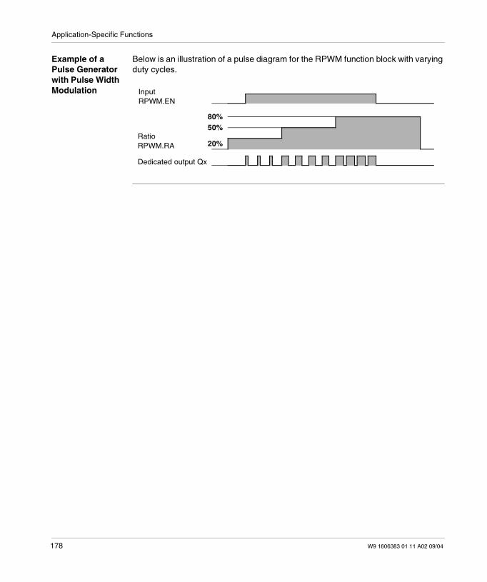
Application-Specific Functions
Example of aPulse Generatorwith Pulse WidthModulation
Below is an illustration of a pulse diagram for the RPWM function block with varyingduty cycles.
RatioRPWM.RA 20%
50%80%
Dedicated output Qx
InputRPWM.EN
178 W9 1606383 01 11 A02 09/04
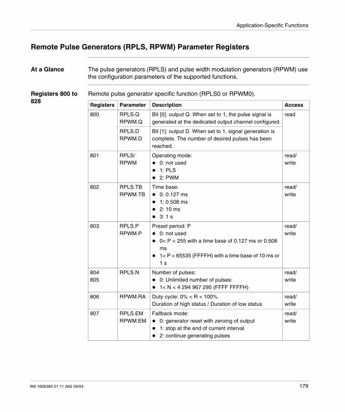
Application-Specific Functions
Remote Pulse Generators (RPLS, RPWM) Parameter Registers
At a Glance The pulse generators (RPLS) and pulse width modulation generators (RPWM) usethe configuration parameters of the supported functions.
Registers 800 to828
Remote pulse generator specific function (RPLS0 or RPWM0).
Registers Parameter Description Access
800 RPLS.QRPWM.Q
Bit [0]: output Q. When set to 1, the pulse signal isgenerated at the dedicated output channel configured.
read
RPLS.DRPWM.D
Bit [1]: output D. When set to 1, signal generation iscomplete. The number of desired pulses has beenreached.
801 RPLS/RPWM
Operating mode:0: not used1: PLS2: PWM
read/write
802 RPLS.TBRPWM.TB
Time base:0: 0.127 ms1: 0.508 ms2: 10 ms3: 1 s
read/write
803 RPLS.PRPWM.P
Preset period: P0: not used0< P < 255 with a time base of 0.127 ms or 0.508ms1< P < 65535 (FFFFH) with a time base of 10 ms or1 s
read/write
804805
RPLS.N Number of pulses:0: Unlimited number of pulses:1< N < 4 294 967 295 (FFFF FFFFH)
read/write
806 RPWM.RA Duty cycle: 0% < R < 100%.Duration of high status / Duration of low status
read/write
807 RPLS.EMRPWM.EM
Fallback mode:0: generator reset with zeroing of output1: stop at the end of current interval2: continue generating pulses
read/write
W9 1606383 01 11 A02 09/04 179

Application-Specific Functions
Specific function of RPLS1 or RPWM1.
808 RPLS. ENRPWM.EN
Bit [0]: pulse generation input. When set to 1, the pulsegeneration is produced on the dedicated outputchannel. When set to 0, the output channel is set to 0.
read/write
RPLS. RRPWM.R
Bit [1]: generator reset input. When set to 1, outputs Qand D are reset to 0. The number of pulses generatedover a period T is reset to 0.
Registers Description Access
820...828 Description identical to that for PLS0 or PWM0 functions
Registers Parameter Description Access
180 W9 1606383 01 11 A02 09/04

W9 1606383 01 11 A02 09/04
7
Software InstallationAdvantys Configuration Tool
At a Glance The purpose of the Advantys Configuration Tool is to help the user configure anisland. It generates a mapping image of the registers which are to be enteredmanually into PL7 / TwidoSoft.
Note: Under no circumstances will the software be able to download theconfiguration directly to the island.
181

Software Installation
182 W9 1606383 01 11 A02 09/04

W9 1606383 01 11 A02 09/04
8
Diagnostics of the Advantys OTBIslandOverview
At a Glance Diagnostics of the Advantys OTB island enables us to analyze the behavior of thenetwork by referring to:
The LEDs indicating the communication and I/O status,The communications objects used for diagnostics of the different functions.
What's in thisChapter?
This chapter contains the following topics:
Topic Page
Indicator Lights (LEDs) 184
OTB Island Diagnostics Registers 186
Behavior in the Event of a Fault 190
183
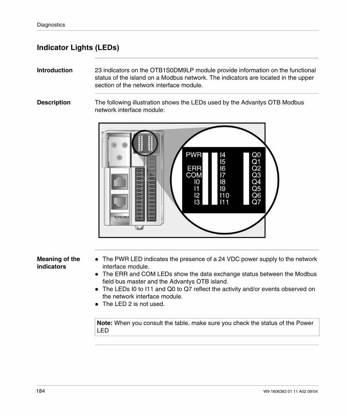
Diagnostics
Indicator Lights (LEDs)
Introduction 23 indicators on the OTB1S0DM9LP module provide information on the functionalstatus of the island on a Modbus network. The indicators are located in the uppersection of the network interface module.
Description The following illustration shows the LEDs used by the Advantys OTB Modbusnetwork interface module:
Meaning of theindicators
The PWR LED indicates the presence of a 24 VDC power supply to the networkinterface module.The ERR and COM LEDs show the data exchange status between the Modbusfield bus master and the Advantys OTB island.The LEDs I0 to I11 and Q0 to Q7 reflect the activity and/or events observed onthe network interface module.The LED 2 is not used.
Note: When you consult the table, make sure you check the status of the PowerLED
184 W9 1606383 01 11 A02 09/04
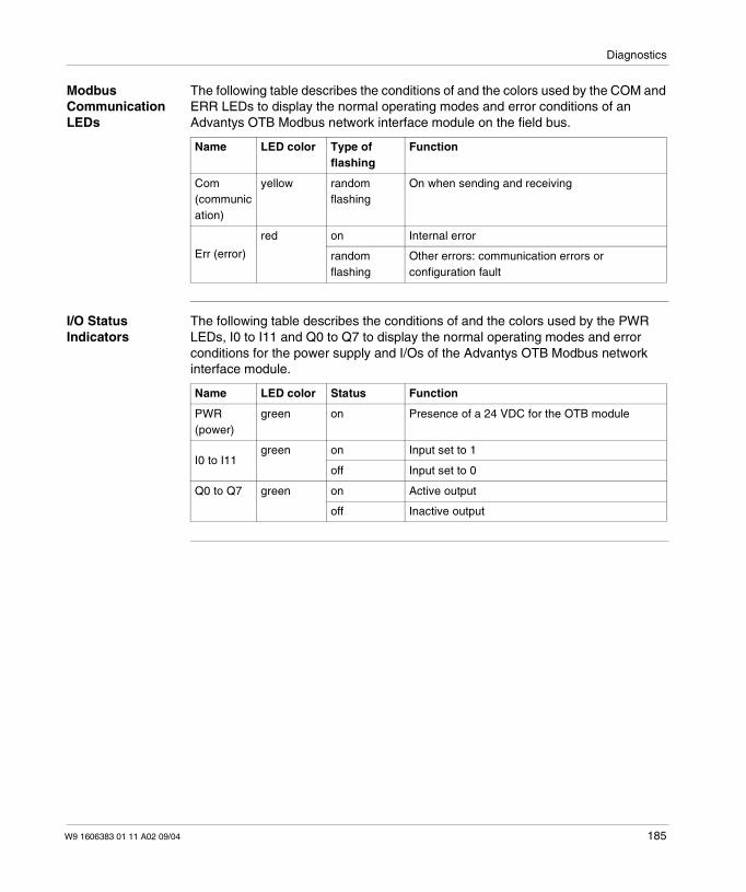
Diagnostics
ModbusCommunicationLEDs
The following table describes the conditions of and the colors used by the COM andERR LEDs to display the normal operating modes and error conditions of anAdvantys OTB Modbus network interface module on the field bus.
I/O StatusIndicators
The following table describes the conditions of and the colors used by the PWRLEDs, I0 to I11 and Q0 to Q7 to display the normal operating modes and errorconditions for the power supply and I/Os of the Advantys OTB Modbus networkinterface module.
Name LED color Type offlashing
Function
Com(communication)
yellow randomflashing
On when sending and receiving
Err (error)
red on Internal error
randomflashing
Other errors: communication errors orconfiguration fault
Name LED color Status Function
PWR(power)
green on Presence of a 24 VDC for the OTB module
I0 to I11green on Input set to 1
off Input set to 0
Q0 to Q7 green on Active output
off Inactive output
W9 1606383 01 11 A02 09/04 185
Diagnostics
OTB Island Diagnostics Registers
At a Glance Diagnostics uses the monitoring parameters of the supported functions. Allparameters in this zone are accessible in read-only.
Registers 900 to917
Registers 900 and 901: Island status
Registers 902 to 907: diagnostics for functions specific to Advantys OTB module(configured functions only)
Registers Function Description
900 Island statusword
Bits [0...8]: not usedBit [9]: communication fault or external faultBits [10...12]: not usedBit [13]: configuration fault (expansion modules missing orbadly configured)Bits [14...15]: not used
901 Expansionmodulestatusword
Bit [0]: status word of first expansion moduleBit [1]: status word of second expansion moduleBit [2]: status word of third expansion moduleBit [3]: status word of fourth expansion moduleBit [4]: status word of fifth expansion moduleBit [5]: status word of sixth expansion moduleBit [6]: status word of seventh expansion module
Note:Bit values:
0: no fault1: fault
Registers Function Description
902 Fast Counter0
Bits [0...8]: not usedBit [9]: configuration consistency errorBits [10...15]: not used
903 Fast Counter1
Description identical to register 902
904 Very FastCounter 0
Description identical to register 902
905 Very FastCounter 1
Description identical to register 902
186 W9 1606383 01 11 A02 09/04
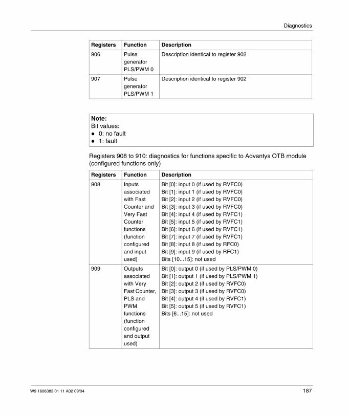
Diagnostics
Registers 908 to 910: diagnostics for functions specific to Advantys OTB module(configured functions only)
906 PulsegeneratorPLS/PWM 0
Description identical to register 902
907 PulsegeneratorPLS/PWM 1
Description identical to register 902
Note:Bit values:
0: no fault1: fault
Registers Function Description
908 Inputsassociatedwith FastCounter andVery FastCounterfunctions(functionconfiguredand inputused)
Bit [0]: input 0 (if used by RVFC0)Bit [1]: input 1 (if used by RVFC0)Bit [2]: input 2 (if used by RVFC0)Bit [3]: input 3 (if used by RVFC0)Bit [4]: input 4 (if used by RVFC1)Bit [5]: input 5 (if used by RVFC1)Bit [6]: input 6 (if used by RVFC1)Bit [7]: input 7 (if used by RVFC1)Bit [8]: input 8 (if used by RFC0)Bit [9]: input 9 (if used by RFC1)Bits [10...15]: not used
909 Outputsassociatedwith VeryFast Counter,PLS andPWMfunctions(functionconfiguredand outputused)
Bit [0]: output 0 (if used by PLS/PWM 0)Bit [1]: output 1 (if used by PLS/PWM 1)Bit [2]: output 2 (if used by RVFC0)Bit [3]: output 3 (if used by RVFC0)Bit [4]: output 4 (if used by RVFC1)Bit [5]: output 5 (if used by RVFC1)Bits [6...15]: not used
Registers Function Description
W9 1606383 01 11 A02 09/04 187
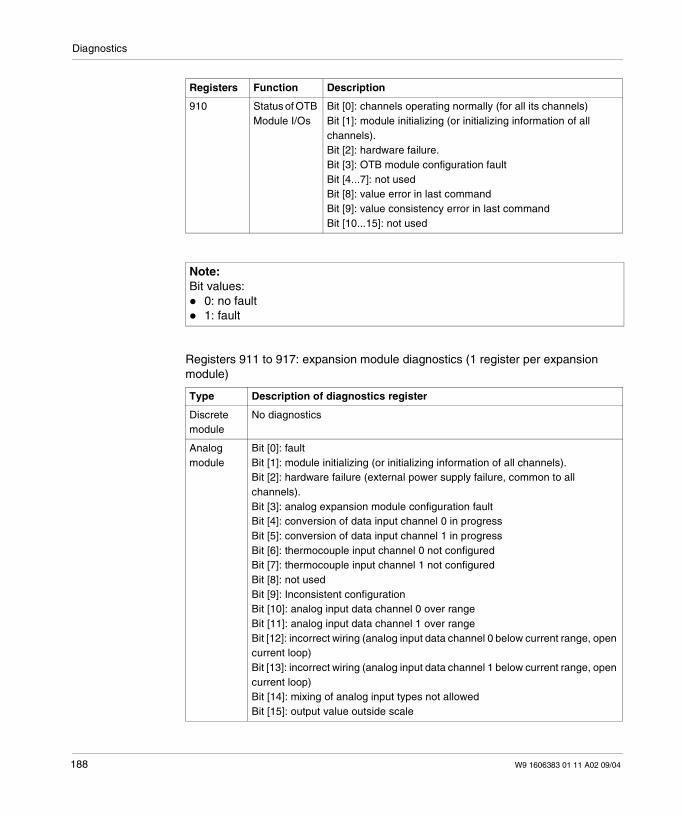
Diagnostics
Registers 911 to 917: expansion module diagnostics (1 register per expansionmodule)
910 Status of OTBModule I/Os
Bit [0]: channels operating normally (for all its channels)Bit [1]: module initializing (or initializing information of allchannels).Bit [2]: hardware failure.Bit [3]: OTB module configuration faultBit [4...7]: not usedBit [8]: value error in last commandBit [9]: value consistency error in last commandBit [10...15]: not used
Note:Bit values:
0: no fault1: fault
Type Description of diagnostics register
Discretemodule
No diagnostics
Analogmodule
Bit [0]: faultBit [1]: module initializing (or initializing information of all channels).Bit [2]: hardware failure (external power supply failure, common to allchannels).Bit [3]: analog expansion module configuration faultBit [4]: conversion of data input channel 0 in progressBit [5]: conversion of data input channel 1 in progressBit [6]: thermocouple input channel 0 not configuredBit [7]: thermocouple input channel 1 not configuredBit [8]: not usedBit [9]: Inconsistent configurationBit [10]: analog input data channel 0 over rangeBit [11]: analog input data channel 1 over rangeBit [12]: incorrect wiring (analog input data channel 0 below current range, opencurrent loop)Bit [13]: incorrect wiring (analog input data channel 1 below current range, opencurrent loop)Bit [14]: mixing of analog input types not allowedBit [15]: output value outside scale
Registers Function Description
188 W9 1606383 01 11 A02 09/04
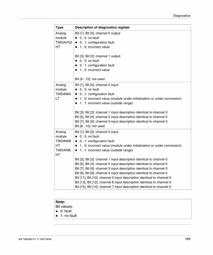
Diagnostics
AnalogmoduleTWDAVO2HT
Bit [1], Bit [0]: channel 0 output0 , 0: no fault0 , 1: configuration fault1 , 0: incorrect value
Bit [3], Bit [2]: channel 1 output0 , 0: no fault0 , 1: configuration fault1 , 0: incorrect value
Bit [4...15]: not used
AnalogmoduleTWDAMI4LT
Bit [1], Bit [0]: channel 0 input0 , 0: no fault0 , 1: configuration fault1 , 0: incorrect value (module under initialization or under conversion)1 , 1: incorrect value (outside range)
Bit [3], Bit [2]: channel 1 input description identical to channel 0Bit [5], Bit [4]: channel 2 input description identical to channel 0Bit [7], Bit [6]: channel 3 input description identical to channel 0Bit [8...15]: not used
AnalogmoduleTWDAMI8HTTWDARI8HT
Bit [1], Bit [0]: channel 0 input0 , 0: no fault0 , 1: configuration fault1 , 0: incorrect value (module under initialization or under conversion)1 , 1: incorrect value (outside range)
Bit [3], Bit [2]: channel 1 input description identical to channel 0Bit [5], Bit [4]: channel 2 input description identical to channel 0Bit [7], Bit [6]: channel 3 input description identical to channel 0Bit [9], Bit [8]: channel 4 input description identical to channel 0Bit [11], Bit [10]: channel 5 input description identical to channel 0Bit [13], Bit [12]: channel 6 input description identical to channel 0Bit [15], Bit [14]: channel 7 input description identical to channel 0
Note:Bit values:
0: fault1: no fault
Type Description of diagnostics register
W9 1606383 01 11 A02 09/04 189

Diagnostics
Behavior in the Event of a Fault
Management ofIsland in theEvent of a Fault
If a fault occurs on one of the modules, the module behaves in the following way:island switches to fallback mode,impossible to read / write (exchange report 04),possible to read exchange registers 900 to 917.
190 W9 1606383 01 11 A02 09/04
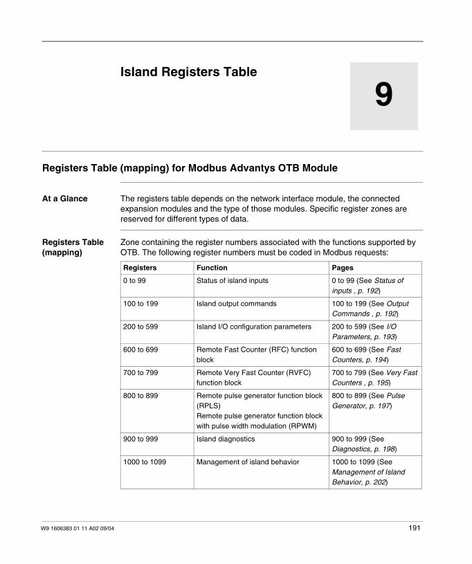
W9 1606383 01 11 A02 09/04
9
Island Registers TableRegisters Table (mapping) for Modbus Advantys OTB Module
At a Glance The registers table depends on the network interface module, the connectedexpansion modules and the type of those modules. Specific register zones arereserved for different types of data.
Registers Table(mapping)
Zone containing the register numbers associated with the functions supported byOTB. The following register numbers must be coded in Modbus requests:
Registers Function Pages
0 to 99 Status of island inputs 0 to 99 (See Status ofinputs , p. 192)
100 to 199 Island output commands 100 to 199 (See OutputCommands , p. 192)
200 to 599 Island I/O configuration parameters 200 to 599 (See I/OParameters, p. 193)
600 to 699 Remote Fast Counter (RFC) functionblock
600 to 699 (See FastCounters, p. 194)
700 to 799 Remote Very Fast Counter (RVFC)function block
700 to 799 (See Very FastCounters , p. 195)
800 to 899 Remote pulse generator function block(RPLS)Remote pulse generator function blockwith pulse width modulation (RPWM)
800 to 899 (See PulseGenerator, p. 197)
900 to 999 Island diagnostics 900 to 999 (SeeDiagnostics, p. 198)
1000 to 1099 Management of island behavior 1000 to 1099 (SeeManagement of IslandBehavior, p. 202)
191
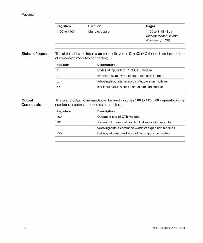
Mapping
Status of inputs The status of island inputs can be read in zones 0 to XX (XX depends on the numberof expansion modules connected).
OutputCommands
The island output commands can be read in zones 100 to 1XX (XX depends on thenumber of expansion modules connected).
1100 to 1108 Island structure 1100 to 1108 (SeeManagement of IslandBehavior, p. 202)
Registers Function Pages
Register Description
0 Status of inputs 0 to 11 of OTB module
1 first input status word of first expansion module
... following input status words of expansion modules
XX last input status word of last expansion module
Registers Description
100 Outputs 0 to 8 of OTB module
101 first output command word of first expansion module
... following output command words of expansion modules
1XX last output command word of last expansion module
192 W9 1606383 01 11 A02 09/04
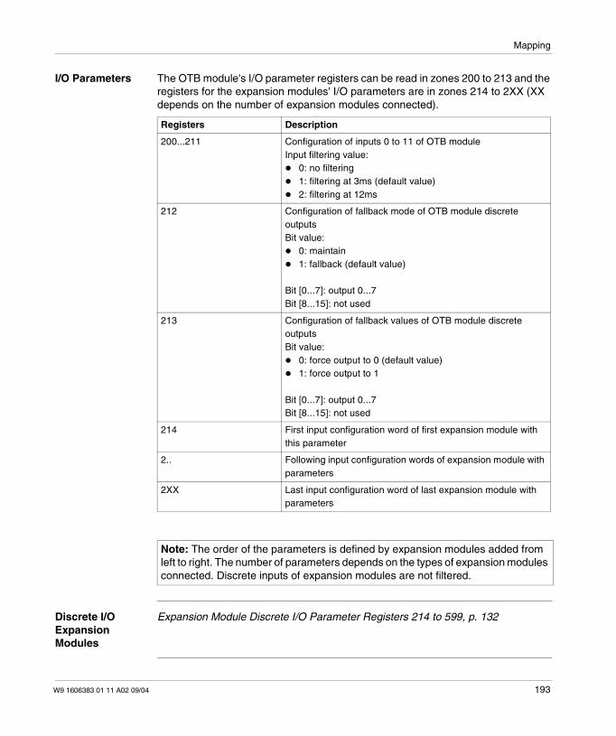
Mapping
I/O Parameters The OTB module's I/O parameter registers can be read in zones 200 to 213 and theregisters for the expansion modules' I/O parameters are in zones 214 to 2XX (XXdepends on the number of expansion modules connected).
Discrete I/OExpansionModules
Expansion Module Discrete I/O Parameter Registers 214 to 599, p. 132
Registers Description
200...211 Configuration of inputs 0 to 11 of OTB moduleInput filtering value:
0: no filtering1: filtering at 3ms (default value)2: filtering at 12ms
212 Configuration of fallback mode of OTB module discreteoutputsBit value:
0: maintain1: fallback (default value)
Bit [0...7]: output 0...7Bit [8...15]: not used
213 Configuration of fallback values of OTB module discreteoutputsBit value:
0: force output to 0 (default value)1: force output to 1
Bit [0...7]: output 0...7Bit [8...15]: not used
214 First input configuration word of first expansion module withthis parameter
2.. Following input configuration words of expansion module withparameters
2XX Last input configuration word of last expansion module withparameters
Note: The order of the parameters is defined by expansion modules added fromleft to right. The number of parameters depends on the types of expansion modulesconnected. Discrete inputs of expansion modules are not filtered.
W9 1606383 01 11 A02 09/04 193
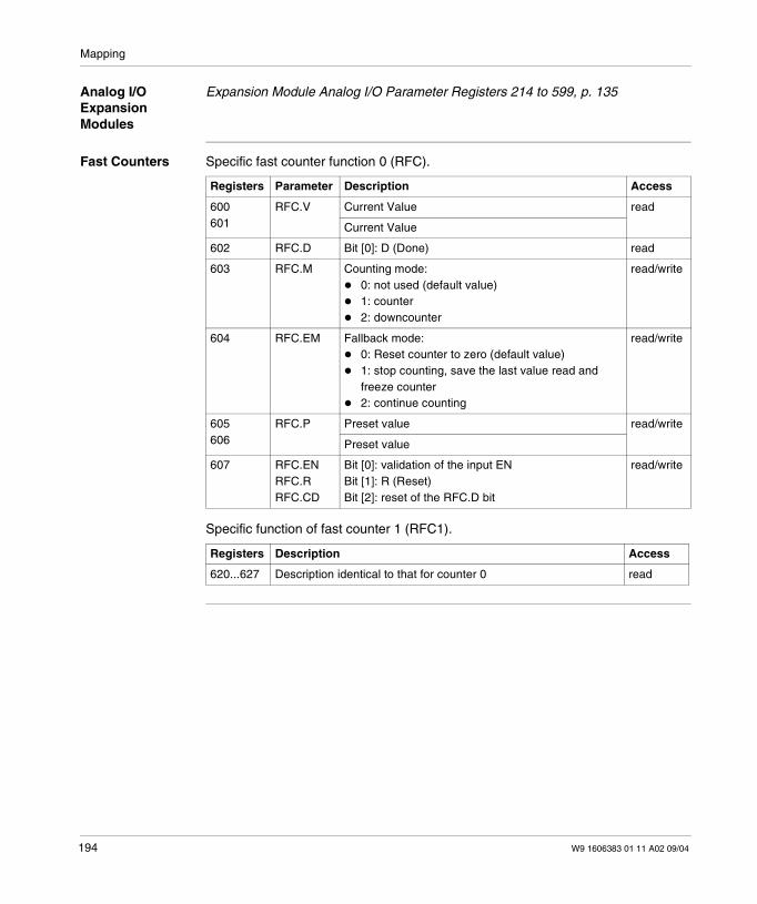
Mapping
Analog I/OExpansionModules
Expansion Module Analog I/O Parameter Registers 214 to 599, p. 135
Fast Counters Specific fast counter function 0 (RFC).
Specific function of fast counter 1 (RFC1).
Registers Parameter Description Access
600601
RFC.V Current Value read
Current Value
602 RFC.D Bit [0]: D (Done) read
603 RFC.M Counting mode:0: not used (default value)1: counter2: downcounter
read/write
604 RFC.EM Fallback mode:0: Reset counter to zero (default value)1: stop counting, save the last value read andfreeze counter2: continue counting
read/write
605606
RFC.P Preset value read/write
Preset value
607 RFC.ENRFC.RRFC.CD
Bit [0]: validation of the input ENBit [1]: R (Reset)Bit [2]: reset of the RFC.D bit
read/write
Registers Description Access
620...627 Description identical to that for counter 0 read
194 W9 1606383 01 11 A02 09/04
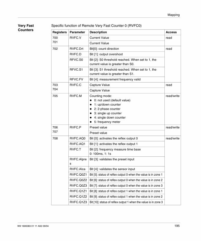
Mapping
Very FastCounters
Specific function of Remote Very Fast Counter 0 (RVFC0)
Registers Parameter Description Access
700701
RVFC.V Current Value read
Current Value
702 RVFC.Drt Bit[0]: count direction read
RVFC.D Bit [1]: output overshoot
RFVC.S0 Bit [2]: S0 threshold reached. When set to 1, thecurrent value is greater than S0.
RFVC.S1 Bit [3]: S1 threshold reached. When set to 1, thecurrent value is greater than S1.
RFVC.FV Bit [4]: measurement frequency valid
703704
RVFC.C Capture Value read
Capture Value
705 RVFC.M Counting mode:0: not used (default value)1: up/down counter2: 2-phase counter3: single up counter4: single down counter5: frequency meter
read/write
706707
RVFC.P Preset value read/write
Preset value
708 RVFC.AQ0 Bit [0]: activates the reflex output 0 read/write
RVFC.AQ1 Bit [1]: activates the reflex output 1
RVFC.T Bit [2]: frequency measure time base0: 100ms, 1: 1s
RVFC.AIpres
Bit [3]: validates the preset input
RVFC.AIca Bit [4]: validates the sensor input
RVFC.Q0Z1 Bit [5]: status of reflex output 0 when the value is in zone 1
RVFC.Q0Z2 Bit [6]: status of reflex output 0 when the value is in zone 2
RVFC.Q0Z3 Bit [7]: status of reflex output 0 when the value is in zone 3
RVFC.Q1Z1 Bit [8]: status of reflex output 1 when the value is in zone 1
RVFC.Q1Z2 Bit [9]: status of reflex output 1 when the value is in zone 2
RVFC.Q1Z3 Bit [10]: status of reflex output 1 when the value is in zone 3
W9 1606383 01 11 A02 09/04 195
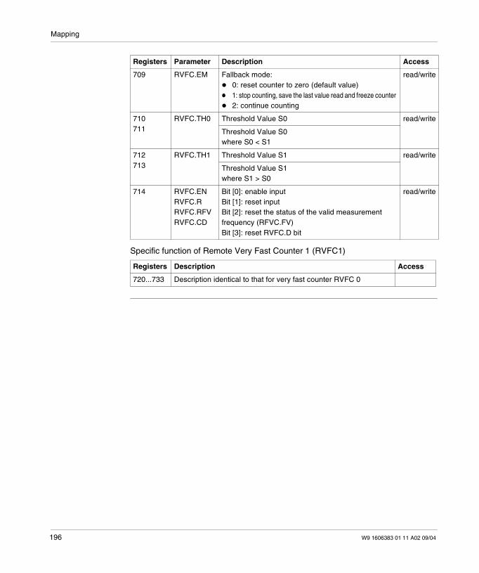
Mapping
Specific function of Remote Very Fast Counter 1 (RVFC1)
709 RVFC.EM Fallback mode:0: reset counter to zero (default value)1: stop counting, save the last value read and freeze counter2: continue counting
read/write
710711
RVFC.TH0 Threshold Value S0 read/write
Threshold Value S0where S0 < S1
712713
RVFC.TH1 Threshold Value S1 read/write
Threshold Value S1where S1 > S0
714 RVFC.ENRVFC.RRVFC.RFVRVFC.CD
Bit [0]: enable inputBit [1]: reset inputBit [2]: reset the status of the valid measurementfrequency (RFVC.FV)Bit [3]: reset RVFC.D bit
read/write
Registers Description Access
720...733 Description identical to that for very fast counter RVFC 0
Registers Parameter Description Access
196 W9 1606383 01 11 A02 09/04
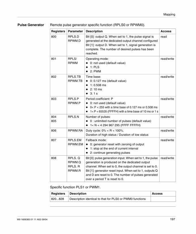
Mapping
Pulse Generator Remote pulse generator specific function (RPLS0 or RPWM0).
Specific function PLS1 or PWM1.
Registers Parameter Description Access
800 RPLS.DRPWM.D
Bit [0]: output Q. When set to 1, the pulse signal isgenerated at the dedicated output channel configuredBit [1]: output D. When set to 1, signal generation iscomplete. The number of desired pulses has beenreached.
read
801 RPLS/RPWM
Operating mode:0: not used (default value)1: PLS2: PWM
read/write
802 RPLS.TBRPWM.TB
Time base:0: 0.127 ms (default value)1: 0.508 ms2: 10 ms3: 1 s
read/write
803 RPLS.PRPWM.P
Period coefficient: P0: not used (default value)0< P < 255 with a time base of 0.127 ms or 0.508 ms1< P < 65535 (FFFFH) with a time base of 10 ms or 1 s
read/write
804805
RPLS.N Number of pulses:0 : unlimited number of pulses (default value)1< N < 4 294 967 295 (FFFF FFFFH)
read/write
806 RPWM.RA Duty cycle: 0% < R < 100%.Duration of high status / Duration of low status
read/write
807 RPLS.EMRPWM.EM
Fallback mode:0: generator reset with zeroing of output1: stop at the end of current interval2: continue generating pulses
read/write
808 RPLS. QRPWM.QRPLS. RRPWM.R
Bit [0]: pulse generation input. When set to 1, the pulsegeneration is produced on the dedicated outputchannel. When set to 0, the output channel is set to 0.Bit [1]: generator reset input. When set to 1, outputs Qand D are reset to 0. The number of pulses generatedover a period T is reset to 0.
read/write
Registers Description Access
820...828 Description identical to that for PLS0 or PWM0 functions
W9 1606383 01 11 A02 09/04 197
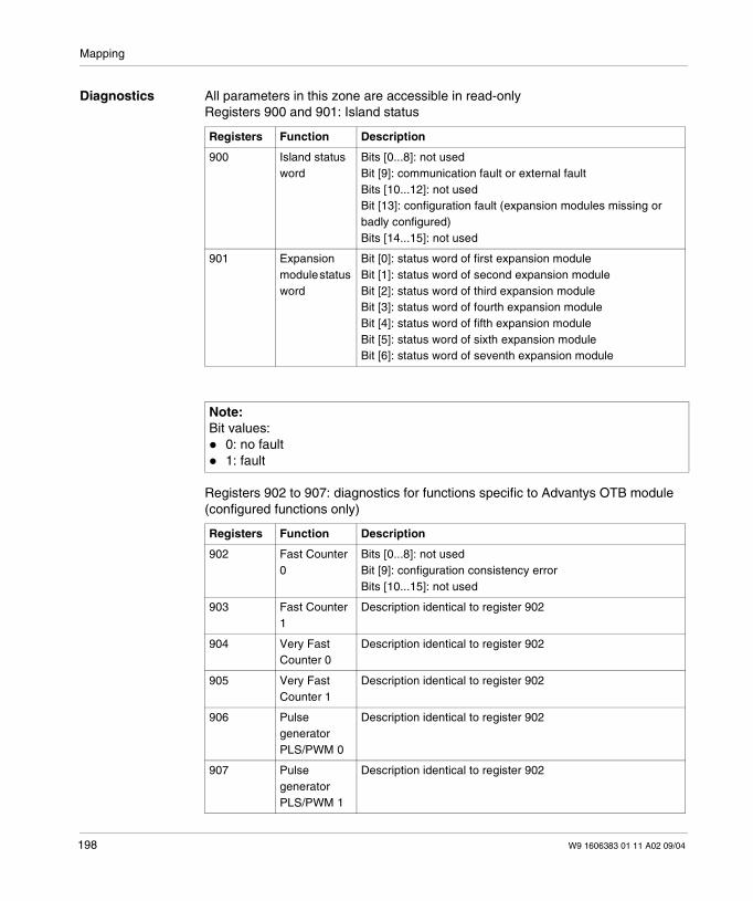
Mapping
Diagnostics All parameters in this zone are accessible in read-onlyRegisters 900 and 901: Island status
Registers 902 to 907: diagnostics for functions specific to Advantys OTB module(configured functions only)
Registers Function Description
900 Island statusword
Bits [0...8]: not usedBit [9]: communication fault or external faultBits [10...12]: not usedBit [13]: configuration fault (expansion modules missing orbadly configured)Bits [14...15]: not used
901 Expansionmodulestatusword
Bit [0]: status word of first expansion moduleBit [1]: status word of second expansion moduleBit [2]: status word of third expansion moduleBit [3]: status word of fourth expansion moduleBit [4]: status word of fifth expansion moduleBit [5]: status word of sixth expansion moduleBit [6]: status word of seventh expansion module
Note:Bit values:
0: no fault1: fault
Registers Function Description
902 Fast Counter0
Bits [0...8]: not usedBit [9]: configuration consistency errorBits [10...15]: not used
903 Fast Counter1
Description identical to register 902
904 Very FastCounter 0
Description identical to register 902
905 Very FastCounter 1
Description identical to register 902
906 PulsegeneratorPLS/PWM 0
Description identical to register 902
907 PulsegeneratorPLS/PWM 1
Description identical to register 902
198 W9 1606383 01 11 A02 09/04
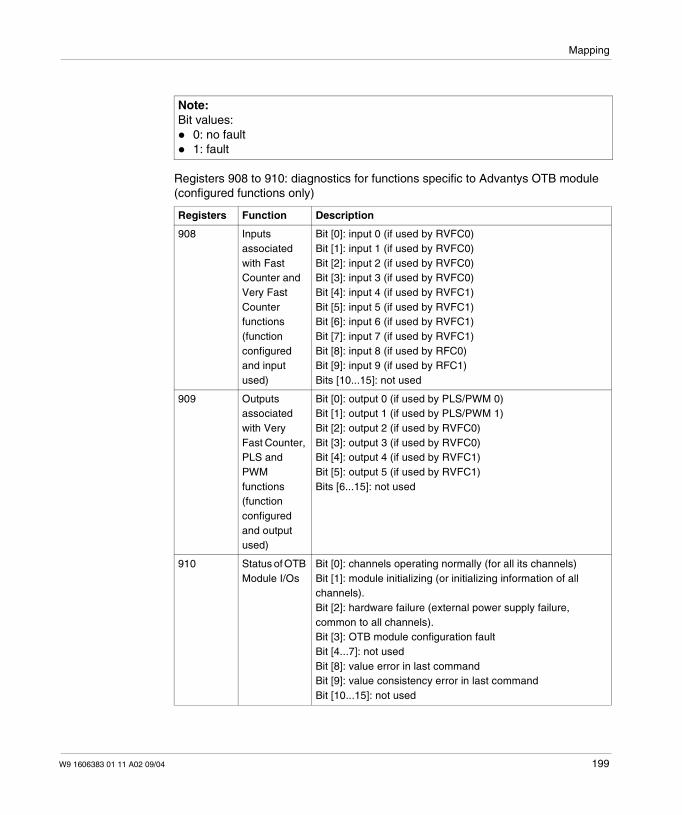
Mapping
Registers 908 to 910: diagnostics for functions specific to Advantys OTB module(configured functions only)
Note:Bit values:
0: no fault1: fault
Registers Function Description
908 Inputsassociatedwith FastCounter andVery FastCounterfunctions(functionconfiguredand inputused)
Bit [0]: input 0 (if used by RVFC0)Bit [1]: input 1 (if used by RVFC0)Bit [2]: input 2 (if used by RVFC0)Bit [3]: input 3 (if used by RVFC0)Bit [4]: input 4 (if used by RVFC1)Bit [5]: input 5 (if used by RVFC1)Bit [6]: input 6 (if used by RVFC1)Bit [7]: input 7 (if used by RVFC1)Bit [8]: input 8 (if used by RFC0)Bit [9]: input 9 (if used by RFC1)Bits [10...15]: not used
909 Outputsassociatedwith VeryFast Counter,PLS andPWMfunctions(functionconfiguredand outputused)
Bit [0]: output 0 (if used by PLS/PWM 0)Bit [1]: output 1 (if used by PLS/PWM 1)Bit [2]: output 2 (if used by RVFC0)Bit [3]: output 3 (if used by RVFC0)Bit [4]: output 4 (if used by RVFC1)Bit [5]: output 5 (if used by RVFC1)Bits [6...15]: not used
910 Status of OTBModule I/Os
Bit [0]: channels operating normally (for all its channels)Bit [1]: module initializing (or initializing information of allchannels).Bit [2]: hardware failure (external power supply failure,common to all channels).Bit [3]: OTB module configuration faultBit [4...7]: not usedBit [8]: value error in last commandBit [9]: value consistency error in last commandBit [10...15]: not used
W9 1606383 01 11 A02 09/04 199
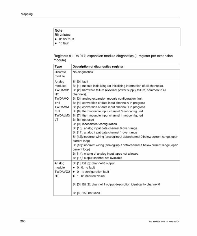
Mapping
Registers 911 to 917: expansion module diagnostics (1 register per expansionmodule)
Note:Bit values:
0: no fault1: fault
Type Description of diagnostics register
Discretemodule
No diagnostics
AnalogmodulesTWDAMI2HTTWDAMO1HTTWDAMM3HTTWDALM3LT
Bit [0]: faultBit [1]: module initializing (or initializing information of all channels).Bit [2]: hardware failure (external power supply failure, common to allchannels).Bit [3]: analog expansion module configuration faultBit [4]: conversion of data input channel 0 in progressBit [5]: conversion of data input channel 1 in progressBit [6]: thermocouple input channel 0 not configuredBit [7]: thermocouple input channel 1 not configuredBit [8]: not usedBit [9]: inconsistent configurationBit [10]: analog input data channel 0 over rangeBit [11]: analog input data channel 1 over rangeBit [12]: incorrect wiring (analog input data channel 0 below current range, opencurrent loop)Bit [13]: incorrect wiring (analog input data channel 1 below current range, opencurrent loop)Bit [14]: mixing of analog input types not allowedBit [15]: output channel not available
AnalogmoduleTWDAVO2HT
Bit [1], Bit [0]: channel 0 output0 , 0: no fault0 , 1: configuration fault1 , 0: incorrect value
Bit [3], Bit [2]: channel 1 output description identical to channel 0
Bit [4...15]: not used
200 W9 1606383 01 11 A02 09/04
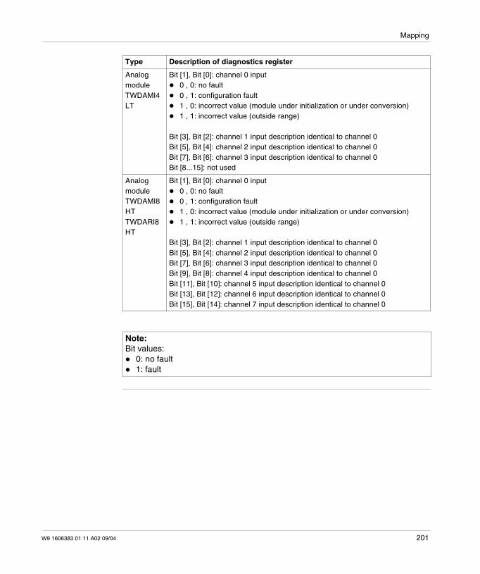
Mapping
AnalogmoduleTWDAMI4LT
Bit [1], Bit [0]: channel 0 input0 , 0: no fault0 , 1: configuration fault1 , 0: incorrect value (module under initialization or under conversion)1 , 1: incorrect value (outside range)
Bit [3], Bit [2]: channel 1 input description identical to channel 0Bit [5], Bit [4]: channel 2 input description identical to channel 0Bit [7], Bit [6]: channel 3 input description identical to channel 0Bit [8...15]: not used
AnalogmoduleTWDAMI8HTTWDARI8HT
Bit [1], Bit [0]: channel 0 input0 , 0: no fault0 , 1: configuration fault1 , 0: incorrect value (module under initialization or under conversion)1 , 1: incorrect value (outside range)
Bit [3], Bit [2]: channel 1 input description identical to channel 0Bit [5], Bit [4]: channel 2 input description identical to channel 0Bit [7], Bit [6]: channel 3 input description identical to channel 0Bit [9], Bit [8]: channel 4 input description identical to channel 0Bit [11], Bit [10]: channel 5 input description identical to channel 0Bit [13], Bit [12]: channel 6 input description identical to channel 0Bit [15], Bit [14]: channel 7 input description identical to channel 0
Note:Bit values:
0: no fault1: fault
Type Description of diagnostics register
W9 1606383 01 11 A02 09/04 201
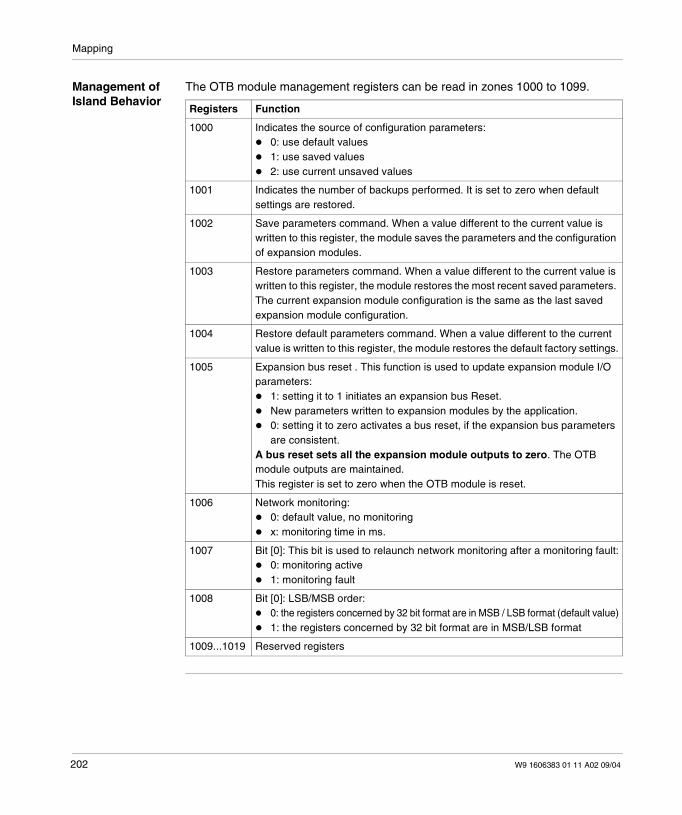
Mapping
Management ofIsland Behavior
The OTB module management registers can be read in zones 1000 to 1099.
Registers Function
1000 Indicates the source of configuration parameters:0: use default values1: use saved values2: use current unsaved values
1001 Indicates the number of backups performed. It is set to zero when defaultsettings are restored.
1002 Save parameters command. When a value different to the current value iswritten to this register, the module saves the parameters and the configurationof expansion modules.
1003 Restore parameters command. When a value different to the current value iswritten to this register, the module restores the most recent saved parameters.The current expansion module configuration is the same as the last savedexpansion module configuration.
1004 Restore default parameters command. When a value different to the currentvalue is written to this register, the module restores the default factory settings.
1005 Expansion bus reset . This function is used to update expansion module I/Oparameters:
1: setting it to 1 initiates an expansion bus Reset.New parameters written to expansion modules by the application.0: setting it to zero activates a bus reset, if the expansion bus parametersare consistent.
A bus reset sets all the expansion module outputs to zero. The OTBmodule outputs are maintained.This register is set to zero when the OTB module is reset.
1006 Network monitoring:0: default value, no monitoringx: monitoring time in ms.
1007 Bit [0]: This bit is used to relaunch network monitoring after a monitoring fault:0: monitoring active1: monitoring fault
1008 Bit [0]: LSB/MSB order:0: the registers concerned by 32 bit format are in MSB / LSB format (default value)1: the registers concerned by 32 bit format are in MSB/LSB format
1009...1019 Reserved registers
202 W9 1606383 01 11 A02 09/04
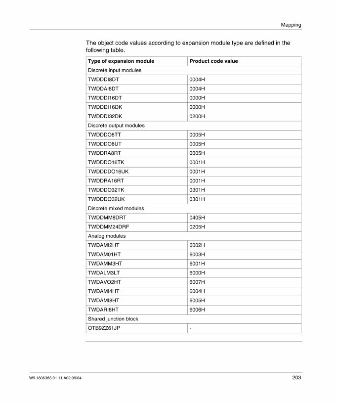
Mapping
The object code values according to expansion module type are defined in thefollowing table.
Type of expansion module Product code value
Discrete input modules
TWDDDI8DT 0004H
TWDDAI8DT 0004H
TWDDDI16DT 0000H
TWDDDI16DK 0000H
TWDDDI32DK 0200H
Discrete output modules
TWDDDO8TT 0005H
TWDDDO8UT 0005H
TWDDRA8RT 0005H
TWDDDO16TK 0001H
TWDDDDO16UK 0001H
TWDDRA16RT 0001H
TWDDDO32TK 0301H
TWDDDO32UK 0301H
Discrete mixed modules
TWDDMM8DRT 0405H
TWDDMM24DRF 0205H
Analog modules
TWDAMI2HT 6002H
TWDAM01HT 6003H
TWDAMM3HT 6001H
TWDALM3LT 6000H
TWDAVO2HT 6007H
TWDAMI4HT 6004H
TWDAMI8HT 6005H
TWDARI8HT 6006H
Shared junction block
OTB9ZZ61JP -
W9 1606383 01 11 A02 09/04 203

Mapping
204 W9 1606383 01 11 A02 09/04

Appendices
At a Glance
Introduction This appendix provides information on common IEC symbols used in this manual.
What's in thisAppendix?
The appendix contains the following chapters:
Chapter Chapter Name Page
A IEC Symbols 207
W9 1606383 01 11 A02 09/04 205

Appendices
206 W9 1606383 01 11 A02 09/04
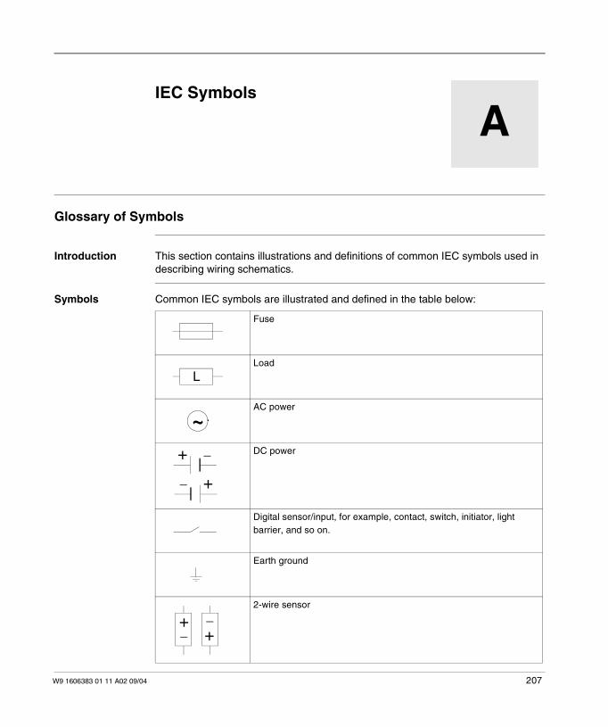
W9 1606383 01 11 A02 09/04
A
IEC SymbolsGlossary of Symbols
Introduction This section contains illustrations and definitions of common IEC symbols used indescribing wiring schematics.
Symbols Common IEC symbols are illustrated and defined in the table below:
Fuse
Load
AC power
DC power
Digital sensor/input, for example, contact, switch, initiator, lightbarrier, and so on.
Earth ground
2-wire sensor
L
~
+ _
+_
+_ +_
207

IEC Symbols
Thermocouple element
208 W9 1606383 01 11 A02 09/04
Glossary
10Base-T An adaptation of the IEEE 802.3 (Ethernet) standard, the 10Base-T standardrequires a twisted pair cable of a maximum segment length of 100m, terminatingwith a RJ-45 connector. A 10Base-T network is a low bandwidth local area networkcapable of transferring data at a maximum speed of 10 Mbit/s.
802.3u, frame A frame format specified in the IEEE 802.3 (Ethernet) standard according to whichthe header species the packet length.
agent 1. SNMP — the server application that runs on a network device. 2. Fipio — a slavedevice on the network.
analog input A module containing circuits that enable analog dc (direct current) input signals tobe converted into digital values that can be handled by the processor. This impliesthat the analog inputs are generally direct values — in other words: a value in thedata table is a direct reflection of the analog signal value.
analog output A module containing circuits that transmit an analog dc (direct current) input signalproportional to a digital input value to the processor module. This implies that theanalog outputs are generally direct values — in other words: a value in the data tabledirectly governs the analog signal value.
!
A
W9 1606383 01 11 A02 09/04 209

Glossary
applicationobject
On networks based on the CAN protocol, application objects represent a specificfunctionality of the device, such as the state of input or output data.
ARP Address Resolution Protocol The IP network layer protocol uses ARP technology tomap an IP address to a MAC (hardware) address.
automaticaddressing
An address is assigned automatically to each preferred island bus I/O module anddevice.
automatic baudrate selection
Automatic assignment and detection of a common baud rate, as well as a device'scapacity to adapt to this rate.
automaticconfiguration
The capacity of island modules to operate with the preset default settings. An islandbus configuration wholly based on a physical assembly of I/O modules.
BootP boot protocol ("bootstrap"). UDP/IP protocol enabling an Internet node to obtain itsIP settings from its MAC address.
BOS Beginning Of Segment. If the island comprises several I/O module segments, anSTB XBE 1200 BOS module is positioned at the start of each extension segment.Its role is to transmit communication messages from the island bus and to generatethe logic power required by the modules on the extension segment.
bus arbiter A master device on a Fipio network.
CAN Controller Area Network. The CAN protocol (ISO 11898) for serial bus networks isdesigned to connect a series of intelligent devices (from different manufacturers)together into intelligent systems for real-time industrial applications. Multi-masterCAN systems provide a high level of data integrity, by implementating messagebroadcast mechanisms and a strict error checking procedure. Initially developed forthe automotive industry, the CAN protocol is now used in a wide range of automationenvironments.
B
C
210 W9 1606383 01 11 A02 09/04
Glossary
CANopen,protocol
An open standard industrial protocol used on the internal communication bus. Thisprotocol can be used to connect any CANopen standard-compliant device to theisland bus.
CI Command Interface
CiA CAN in Automation. The acronym CiA denotes a non-profit making organization ofmanufacturers and users who wish to promote and develop the use of high layerprotocols based on CAN.
COB Communication ObjectA communication object is a unit of transfer (a "message")used on a CAN network. Communication objects indicate specific devicefunctionality. They are specified in the CANopen communication profile.
COMS("CANopenMasterScanner")
island bus scanner.
configuration The arrangement and connections made between the hardware components of asystem, as well as the selected hardware and software options that determine thesystem's operating characteristics.
CRC cyclic redundancy check. The messages that use this error finding mechanism havea CRC field that is calculated by the sender according to the content of the message.The receiving nodes recalculate the CRC field. Any difference between the twocodes indicates a difference between the message sent and that received.
DeviceNet,protocol
DeviceNet is a network based on low level connections and established over CAN,using a serial bus system without a defined application layer. Consequently,DeviceNet defines a layer for the industrial application of the CAN protocol.
DHCP Dynamic Host Configuration Protocol. DHCP is a TCP/IP protocol that enables aserver to assign an IP address based on a role name (host name) to a network node.
D
W9 1606383 01 11 A02 09/04 211
Glossary
differential input An input design in which two wires (+ and -) run from each signal source to the dataacquisition interface. The voltage between the input and the interface ground ismeasured by two high-impedance amplifiers, and the outputs of the two amplifiersare subtracted by a third amplifier to give the difference between the + and - inputs.The voltage common to the two wires is thus eliminated. A differential designeliminates the problem of ground differences encountered with single endconnections. It also minimizes the problem of noise interference between channels.
digital input/output
Another expression used is discrete input/output. Designates an input or outputfeaturing an individual circuit connection to the module corresponding directly to abit or word of the data table storing the value of the signal on this I/O circuit. A digitalI/O gives the control logic discrete access to I/O values.
DIN "Deutsche Industrie Norm". German standardization body that defines dimensionaland engineering standards. These standards are currently recognized worldwide.
EDS Electronic Data SheetThe EDS is a file in standard ASCII format containinginformation on a communication functionality of a network device and the content ofits object dictionary. The EDS also defines device-specific and manufacturer-specific objects.
EIA Electronic Industries Association. Body that draws up data communication andelectrical/electronic standards.
electro-magneticdisturbance
Electro-Magnetic Interference (EMI). Electro-magnetic disturbances are liable tocause interruptions, anomalies or interference in the performance of electronichardware. They occur when a source electronically transmits a signal that interfereswith other devices.
EMC Electro-Magnetic Compatibility. Devices that comply with EMC requirements arecapable of error-free operation within the specified electro-magnetic limits of thesystem.
EOS "End Of Segment". If the island comprises several I/O module segments, anSTB XBE 1000 EOS module is positioned at the start of each extension segment,except the last segment in the island. Its role is to pass on communication messagesfrom the island bus and to transmit the 24 VDC logic power supply to the nextsegment.
E
212 W9 1606383 01 11 A02 09/04
Glossary
Ethernet Wiring and indicator specification for LANs (Local Area Networks) used to connectdevices together on a specific site, such as within a building. Ethernet uses a bus orstar topology to connect different network nodes together.
Ethernet II A frame format according to which the header species the packet type. Ethernet IIis the default frame format for communication with the Advantys STB NIP 2212 NIM.
fallback state A secure state to which any Advantys STB I/O module can revert should thecommunication connection fail.
fallback value The value adopted by a device when it enters the fallback state. Generally, thefallback value is either configured, or is the device's last stored value.
FED_P Extended Fipio, device profile. On a Fipio network, the standard type of deviceprofile for agents whose data length is greater than eight words and less than orequal to 32 words.
Fipio Fieldbus Interface Protocol (FIP) open fieldbus protocol and standard, compliantwith FIP/World FIP standards. Fipio is designed to provide configuration, setup, dataexchange and low-level diagnostics services.
Flash memory Flash memory is a type of memory that is non-volatile (or remanent) but liable to beoverwritten. Data is stored in a special EEPROM chip, which is erasable andreprogrammable.
FRD_P Reduced Fipio, device profile. On a Fipio network, the standard type of device profilefor agents whose data length is less than or equal to two words.
FSD_P Standard Fipio, device profile. On a Fipio network, the standard type of device profilefor agents whose data length is greater than two words and less than or equal toeight words.
full scale The maximum level in a specific range. For an analog input circuit, for example, themaximum authorized voltage or current is said to be at full scale when a minimalincrease in level would cause an authorized range overrun.
function block A function block performs a specific automation function, such as speed control. Afunction block includes configuration data and a set of operating parameters.
F
W9 1606383 01 11 A02 09/04 213
Glossary
function code A function code is a series of instructions ordering one or more slave devices,located at one or more specified addresses, to perform a type of action, for exampleto read a set of data registers and to respond by writing the content of the set inquestion.
gateway A program or hardware component whose role is to relay data between networks.
global_ID global_identifier. 16-bit integer that uniquely identifies the position of a device on anetwork. This global identifier (global_ID) is a symbol address universallyrecognized by all other devices on the network.
GSD Generic Slave Data file. A GSD file is a device description file supplied by themanufacturer, which defines the functionality of the device concerned on aProfibus DP network.
HMI human-machine interface A user interface (usually graphic) for industrial devices.
HMI human-machine interface A user interface (usually graphic) for industrial devices.
hotswap Designates a procedure that allows a component to be replaced without needing tointerrupt system operation. It is sometimes called a "hot" replacement although thisexpression can be confusing.
HTTP HyperText Transfer Protocol. The protocol used for communication between a webserver and a client browser.
I/O connectionbase
Mounting device for an I/O module, allowing it to be attached to a DIN rail andconnected to the island bus. It can be used as a connection channel via which themodule can receive a 24 VDC or 115/230 VAC power supply from an input or outputpower bus, distributed by a PDM.
G
H
I
214 W9 1606383 01 11 A02 09/04

Glossary
I/O module In a programmable control system, an I/O module communicates directly withsensors or actuators used in the machine or process. This module is the componentthat is installed in the I/O connection base and establishes the electrical connectionsbetween the controller and the fieldbuses. The functionalities common to all I/Omodules are offered in a range of signal capacities and levels.
I/O scanning Continual polling of Advantys STB I/O modules, performed by the COMS in order toobtain data bits and state, error and diagnostics information.
IEC International Electrotechnical Commission. Commission officially founded in 1906and devoted to the advancement of theory and practice in the following sciences:electrical engineering, electronic engineering, information technology and computerengineering. The IEC 1131 standard covers industrial automation equipment.
IEC 1 type input Type 1 digital inputs support sensor signals from mechanical switching devices suchas contact relays and push-buttons operating under normal climatic conditions.
IEC 1+ type input Type 1+ digital inputs support sensor signals from mechanical switching devicessuch as contact relays and push-buttons (under normal to moderate climaticconditions), three-wire proximity switches and two-wire proximity switches with thefollowing characteristics:
a voltage drop of less than or equal to 8 Va minimum operating current capacity of less than or equal to 2 mAa maximum current in blocked state of less than or equal to 0.8 mA
IEC 2 type input Type 2 digital inputs support sensor signals from solid-state devices and mechanicalswitching devices such as contact relays, push-buttons (under normal to rigorousclimatic conditions), and two or three-wire proximity switches.
IEEE Institute of Electrical and Electronics Engineers, Inc. An international association forthe standardization and evaluation of compliance in all areas of electro-technology,including electricity and electronics.
industrial I/O Advantys STB I/O modules are designed, at moderate cost, generally for continuoushigh-yield cycle applications. Modules of this type are often characterized by IECstandard threshold indices, and generally offer user-definable configuration options,internal protection, good resolution and fieldbus wiring options. They are designedto operate in moderate to high temperatures.
input filter The period for which a sensor must keep its signal activated/deactivated before theinput module detects a change of state.
W9 1606383 01 11 A02 09/04 215
Glossary
input polarity The polarity of an input channel determines when the input module sends a 1 (one)and when it sends a 0 (zero) to the master controller. If the polarity is normal, aninput channel will send a 1 (one) to the controller as soon as its fieldbus sensor isactivated. If the polarity is reversed, an input channel will send a 0 (zero) to thecontroller as soon as its fieldbus sensor is activated.
input responsetime
The time required for an input channel to receive a signal from a fieldbus sensor andpass it on to the island bus.
INTERBUS,protocol
The INTERBUS fieldbus protocol complies with a master/slave network model usingan active ring topology, in which all devices are integrated to form a closed channelof transmission.
IP Internet Protocol. The part of the family of TCP/IP protocols that keeps track of theinternet addresses of nodes, routes outgoing messages and recognizes incomingmessages.
LAN Local Area Network. Designates a data communication network covering shortdistances.
light industrial I/O
An Advantys STB I/O module designed at very low cost for less demandingenvironments (intermittent, low yield cycles). Modules of this type are for use atmore moderate temperatures, subject to less strict compliance and homologationrequirements and under circumstances where limited internal protection isacceptable. These modules offer significantly less user-configurable options or noneat all.
linearity Measurement of how closely a characteristic follows a linear function.
LSB Least Significant Bit or Least Significant Byte. The part of a number, address or fieldthat is written as the value furthest to the right in conventional hexadecimal or binarynotation.
MAC address Medium Access Control. 48-bit number that is unique on a network, and isprogrammed into every network card or device at the time of manufacture.
L
M
216 W9 1606383 01 11 A02 09/04
Glossary
mandatorymodule
If an Advantys STB I/O module is configured as mandatory, it has to be present andin good operating condition as part of the island configuration for the latter to befunctional. If a mandatory module fails or is removed from its slot on the island bus,the whole island switches to Pre-operational mode, and ceases operation. Bydefault, no I/O module is mandatory. The Advantys configuration software must beused to set this parameter.
master/slavemodel
In a network using a master/slave model, the direction of control is always from themaster to slave devices.
MIB Management Information Base. Public database containing the networkmanagement variables for a device compatible with SNMP (Simple NetworkManagement Protocol). Each network management variable is identified by aunique name, a standardized description and the position that it is assigned in thedata structure of an internet Management Information Base (MIB). In this publicdatabase, Schneider Electric has its own MIB extension (3833). Schneider's privateManagement Information Base itself contains another MIB that is private anddevoted to Transparent Factory Ethernet (TFE). These private MIB extensionsenable Schneider to provide its proprietary and non-proprietary networkmanagement software with additional information on network managementvariables.
Modbus Modbus is an application layer messaging protocol. Modbus enables client andserver communication between devices connected via different types of bus ornetwork. Modbus offers a large number of services specified by function codes.
MSB Most Significant Bit or Most Significant Byte. The part of a number, address or fieldthat is written as the value furthest to the left in conventional hexadecimal or binarynotation.
N.C. contact Designates a normally closed contact. Also called break contacts. A pair of contactrelays that is closed when the relay coil is low and open when it is energized.
N.O. contact Normally Open contact Also called make contacts. A pair of contact relays that isopen when the relay coil is low and closed when it is energized.
NEMA National Electrical Manufacturers Association.
network cycletime
The time it takes a master to complete a single scan of all I/O modules configuredon a network device. This period is generally expressed in microseconds.
N
W9 1606383 01 11 A02 09/04 217
Glossary
NIM Network Interface Module. This module provides the interface between an islandbus and the fieldbus network to which the island belongs. The NIM's built-in powersupply supplies logic power of 5 V to Advantys STB I/O modules and 24 V electricalpower, as required, to support I/O modules. The NIM also includes a RS-232 portthat is used to establish a connection with the Advantys configuration software.
NMT network management.NMT protocols offer services for network initialization, errorchecking and checking device states.
object dictionary Sometimes referred to as the "object directory", this element of the CANopen devicemodel provides the plan for the internal structure of CANopen devices (inaccordance with the DS-401 CANopen profile). The object dictionary of a givendevice is a conversion table describing the data types, the communication objectsand the application objects used by the device. By accessing the object dictionarystructure of a specific device via the CANopen fieldbus, you can anticipate itsnetwork behavior enabling you to design a distributed application in which it can beimplemented.
open industrialcommunicationnetwork
A distributed communication network for industrial environments, based on openstandards (EN 50235, EN50254 and EN50170, to citer a few) that enable data to beexchanged between devices from different manufacturers.
output filter The time it takes for an output channel to transmit change of state information to anactuator once the output module has received updated data from the NIM.
output polarity The polarity of an output channel determines when the output module activates itsfieldbus actuator and when it deactivates. If the polarity is normal, an output channelwill activate its actuator as soon the master controller sends it the value 1. If thepolarity is reversed, an output channel will activate its actuator as soon the mastercontroller sends it the value 0.
output responsetime
The time it takes for an output module to receive an output signal from the island busand transmit it to its fieldbus actuator.
parameterize To specify the value required by a device attribute during execution.
O
P
218 W9 1606383 01 11 A02 09/04
Glossary
PDM Power Distribution Module. Module that distributes an AC or DC fieldbus powersupply to a group of modules positioned immediately to its right on the island bus.The PDM provides a separate fieldbus power supply terrain to the input modulesand the output modules. It is essential that all the I/Os grouped immediately to theright of a PDM are of the same voltage group (+ 24 VDC, 115 VAC or 230 VAC.
PDO, object Process Data Object.On networks based on CAN technology, PDOs (Process DataObjects) are transmitted as broadcast messages without confirmation or sent froma producer device to a consumer device. The transmitted PDO (TxPDO) from theproducer device has a specific identifier corresponding to the PDO (RxPDO)received from client devices.
PE Protective Earth Current return line running the length of the bus, destined to carryleakage currents generated by a sensor or actuator in the control system.
peer to peercommunications
In peer to peer communications, there is no master/slave or client/server relation.Messages are exchanged between entities of comparable or equivalent levels offunctionality, without needing to pass via a third party such as a master device.
PLC Programmable Logic Controller. The PLC is the nerve center of the industrialmanufacturing process. Such a device is said to "automate a process", in contrastto a relay control system. These PLCs are in fact simply computers designed tosurvive under the sometimes harsh conditions of an industrial environment.
preferred module I/O module that functions as an auto-addressable node on an Advantys STB islandbus, but which does not have the same form factor as a standard Advantys STB I/Omodule and which, therefore, cannot be installed in an I/O connection base. Apreferred device is connected to the island bus via an STB XBE 1000 EOS moduleand an STB XCA 100x bus extension cable. The island bus can be extended toanother preferred module or to another Advantys STB I/O segment. If the device ormodule is the last one on the island bus, it must be terminated using a 120 Ω busterminator resistor (or "bus resistance jack").
Premiumnetworkinterface
An Advantys STB network interface module designed at relatively high cost tosupport a large number of modules and provide high data transfer capacities (forweb servers, for example) and other diagnostics on the island bus.
process I/O An Advantys STB I/O module designed specially to operate in extreme temperatureranges, in compliance with IEC type 2 thresholds. Modules of this type are generallycharacterized by advanced built-in diagnostics capacities, high resolution; user-definable configuration options, and stricter homologation criteria.
W9 1606383 01 11 A02 09/04 219
Glossary
process image Section of NIM firmware used to store real-time data for the data exchange process.The process image includes an input buffer that contains current state informationand data from the island bus, and an output buffer that groups all current outputsfrom the island bus as they are received from the fieldbus master.
producer/consumer model
On networks employing a producer/consumer model, data packets are identified bytheir data content rather than their physical position. All nodes "listen" to the networkand consume data packets with identifiers corresponding to their functionality.
Profibus DP Profibus Decentralized Peripheral. An open bus system that uses an electricalnetwork based on a shielded two-wire cable or an optical network based on a fiberoptic cable. DP transmission is designed to enable high-speed cyclical exchange ofdata between the PLC processor and distributed I/O devices.
ranking Ranking (or prioritization) is an optional functionality enabling you to selectivelyidentify digital input modules to be scanned more frequently than others when theNIM logically scans the island bus.
reflex action The execution of a simple logic command function configured locally on an I/Omodule of the island bus. Reflex actions are executed by island bus modules on datafrom various locations on the island, such as input and output modules or the NIM.For example, reflex actions include copy and compare operations.
repeater A connection device that extends the authorized length of a bus.
reverse polarityprotection
In a circuit, use of a diode to protect against damage and any inadvertent operationsthat may be caused if the polarity of the applied power is accidentally reversed.
rms Root Mean Square. The effective value of an alternating current, corresponding tothe DC value producing the same heating effect. The rms value is calculated bytaking the square root of the mean of the sum of the squares of the instantaneousamplitude of a given full cycle. For a sinusoidal wave, the rms value corresponds to0.707 of the peak value.
R
220 W9 1606383 01 11 A02 09/04
Glossary
role name A unique logical personal identifier, generated by the client and assigned to anEthernet Modbus TCP/IP NIM. Two methods can be used to create the role name:either by using a combination of manual settings on a numerical rotary switch andthe reference number of the STB NIP 2212 NIM, or by going to the role nameconfiguration web page. Once you have configured a valid role name for theSTB NIP 2212 NIM, the DHCP server will use this value to identify the island onpower up.
RTD Resistive Temperature Detector. Also known as a Resistance Temperature Deviceor thermocoupler. An RTD consists of a temperature transducer composed ofconducting wires generally made of platinum, nickel, copper or nickel-iron. The RTDgenerates a variable resistance within a specific temperature range.
Rx reception. On a CAN, for example, a PDO is described as an RxPDO of the devicethat receives it.
SAP Service Access Point. The point at which the services of a communications layer, asdefined in the ISO OSI reference model, can be accessed from the next layer.
SCADA Supervisory Control And Data Acquisition. In an industrial environment, theseoperations are generally performed by computers.
SDO, object Service Data Object. On CAN networks, the fieldbus master (CANopen) uses SDOmessages for (read/write) access to the network node object dictionaries.
segment Designates a group of I/O modules and power modules connected together on anisland bus. Any island must include at least one segment and can have a maximumof seven segments. The first module (furthest to the left) of a segment must providea power bus and send communications from the island bus to the I/O moduleslocated to its right. In the main segment, this function is always performed by a NIM.In an extension segment, the STB XBE 1200 BOS module assumes this function.
SELV Safety Extra Low Voltage.A secondary circuit designed and protected to ensure thatthe voltage measured between two accessible components (or between anaccessible component and the PE terminal for Class 1 devices) never exceeds aspecified safety value under normal or single fault conditions.
S
W9 1606383 01 11 A02 09/04 221
Glossary
SIM Subscriber Identification Module. Initially designed for the authentication of mobiletelephone subscribers, SIM cards are now used for many other applications. TheAdvantys STB configuration software enables you to store configuration datacreated or modified using the software on a removable SIM card, and then savethem to the NIM's flash memory.
single-endedinputs
An analog input design in which a cable from each signal source is connected to thedata acquisition interface and the difference between the signal and the ground ismeasured. The success of this design technique requires two conditions to be met:the signal source must be connected to the ground and, in addition, the signalground and the data acquisition interface ground (the PDM ground wire) must havethe same potential.
sink load (orpositive logicload)
Designates an output which, when activated, receives DC current from its load.
Size 1connection base
Mounting device for an Advantys STB module, allowing it to be attached to a DINrail and connected to the island bus. This base is 13.9 mm wide and 128.25 mmhigh.
Size 2connection base
Mounting device for an Advantys STB module, allowing it to be attached to a DINrail and connected to the island bus. This base is 18.4 mm wide and 128.25 mmhigh.
Size 3connection base
Mounting device for an Advantys STB module, allowing it to be attached to a DINrail and connected to the island bus. This base is 28.1 mm wide and 128.25 mmhigh.
SM_MPS State Management Message Periodic Services. Designates the application andnetwork management services used for controlling processes, data exchange, errorreport generation, and for automatic warning in the event of an error on the Fipionetwork.
SNMP Network Management Protocol. The standard UDP/IP protocol used formanaging IP network nodes.
source load Also called a negative logic load. Designates a load with a directed input current.This load must come from a current source.
Split I/O An I/O module design providing a modest number of channels (generally betweentwo and six) in a very compact unit. The purpose of such a design is to enable thesystem manufacturer or integrator to only buy as many I/Os as he really needs,whilst being able to distribute these I/Os around the machine in an efficient andmechatronic manner.
222 W9 1606383 01 11 A02 09/04
Glossary
standardnetworkinterface
An Advantys STB network interface module developed at a reasonable cost tosupport the configuration and baud rate capacities that suit most standardapplications on the island bus.
STD_P Standard Profile. On a Fipio network, a standard profile includes a fixed set ofconfiguration and operation parameters for an agent device. This profile is based onthe number of modules the device contains, and on the total length of its data. Threetypes of standard profile are available: FRD_P (Fipio Reduced Device Profile),FSD_P (Fipio Standard Device Profile), and FED_P (Fipio Extended Device Profile).
stepper motor Specialist DC motor used to obtain a discrete positioning without feedback.
sub-mask Number used to identify the sub-network.
sub-network Network segment that shares a network address with the other parts of a network.Any sub-network can be physically and/or logically independent from the rest of thenetwork. It is up to a part of the Internet address – the sub-network number – toidentify the sub-network. This number is not acknowledged during IP routing.
suppression ofover-voltage
Process consisting of absorbing and limiting transient over-voltage on an incomingAC line or a control circuit. Specially designed metal oxide limiters (varistors) andRC networks are frequently used as over-voltage suppression mechanisms.
suppressor A circuit generally used to suppress inductive loads, comprising as standard aresistor with a condenser (case of an RC suppressor) and/or a metal oxide limiterplaced through the AC load.
TC Thermocoupler. A TC (thermocoupler) comprises a bi-metal temperature transducerthat gives a temperature value by measuring the difference in potential caused bythe joining of two different metals, at different temperatures.
TCP Transmission Control Protocol. Connection-based transport layer protocol thatprovides a reliable simultaneous bi-directional transmission of data. TCP is part ofthe TCP/IP protocol suite.
telegram A data packet used in serial communications.
TFE Transparent Factory Ethernet. Schneider Electric’s open PLC architecture, basedon TCP/IP protocol.
T
W9 1606383 01 11 A02 09/04 223
Glossary
Tx Transmission.On a CAN, for example, a PDO is described as an TxPDO of thedevice that transmits it.
UDP User Datagram Protocol. A protocol in unconnected mode to which messages aredistributed to a recipient computer in the form of a datagram (data telegram). UDPprotocol is generally provided at the same time as Internet protocol (UPD/IP).
varistor Also known as a limiter. This is a two-electrode semi-conductor device with a non-linear varistance that causes a considerable drop as the applied voltage graduallyincreases. A varistor is used to remove transient over-voltages.
voltage group A group of Advantys STB I/O modules with the same voltage requirements (forexample: AC modules), installed immediately to the right of the power distributionmodule (PDM) in question, and physically separated from modules with othervoltage requirements (DC). Never mix different voltage group modules within thesame module group.
watchdog timer Tracking clock that controls a cyclical process and which is cleared at the end ofeach cycle. The watchdog timer generates an error when it exceeds the assigneddelay time.
U
V
W
224 W9 1606383 01 11 A02 09/04
CBAIndex
AAnalog I/O modules
Dimensions, 27Input specifications, 96Mounting positions, 33Output specifications, 98Overview, 93Parts description, 94Specifications, 16, 95Wiring schematics, 100
BBaud rate
Configuration, 115Selection, 115
CCabinet assembly precautions
Network interface modules, 35Cables, 17Characteristics
DC input of a network interface module,55Network interface module, 13Normal operation of a network interfacemodule, 53Relay output of a network interfacemodule, 58Sink transistor output of a network
W9 1606383 0111A01 07/2004
interface module, 57Source transistor output of a networkinterface module, 57Supply of a network interface module, 54
Communication block moduleCharacteristics, 17
Communication moduleMounting hole layout, 30
CommunicationsField bus, 113
ConfigurationHardware, 18
Connection of the field bus or network, 63
DData exchange, 185Diagnostics
LEDs, 185
225
Index
Digital I/O modulesI/O usage limits, 74, 80Input internal circuit, 80Internal circuit, 74Mounting positions, 33Operating range, 73, 80Output delay, 76, 81Overview, 67Parts description, 70Relay output contact, 81Specifications, 14, 72, 76, 77, 78, 79, 81Transistor sink output contact, 82Transistor source output contact, 82Wiring schematics, 83
DimensionsAnalog I/O modules, 27Discrete I/O modules, 27, 28, 29Network interface module, 26
DIN rail15 mm AM1DE200 rail, 43
Discrete I/OFiltering, 150Remote Fast Counters, 150Remote Pulse Generators, 150Remote Very Fast Counters, 150
Discrete I/O modulesDimensions, 27, 28, 29
EEncoder Wheel, 112, 114Encoder wheel
Configuration of the baud rate, 115Parts description, 112, 114
Encoder wheelsNode Address, 113
Expansion I/O Modules Analog I/O modules,72Expansion I/O Modules Digital I/O modules,72Expansion module
Assembly of an expansion module, 36Disassembly of an expansion module, 39
Expansion modulesMounting hole layout, 31
226
FFast counter
RFC, 21Field bus
Address, 112Address, specifications, 112Baud rate, 114Speed, specifications, 114
Field bus interfacePin assignment, 108
Field bus masterLED, 185
FilteringDiscrete I/O, 150
Function blockRPWM, 175
II/O island
Overview, 23Resistance jacks, 23
I/O usage limitsDigital I/O modules, 74, 80
Identification Objects, 119Identification report, 119IEC symbols, 207Indicators
Overview, 184Input internal circuit
Digital I/O modules, 80Installation on a DIN rail, 41Installation preparation, 32Internal circuit
Digital I/O modules, 74Internal input circuit
Network interface module, 56Island
Address, 112Baud rate, 115Node Address, 113Status, 184
W9 1606383 0111A01 07/2004
Index
LLEDs
COM, 185ERR, 185I0, I11, 185PWR, 185Q0, Q7, 185
MMaximum hardware configuration, 18Modbus, 117
Field bus interface, 108Modbus function codes, 118Modbus network, 106Modbus protocol, 117Module
Installation on a DIN rail, 41Overview, 51Physical description, 52Removal of a DIN rail, 42
Mounting hole layoutCommunication module, 30Expansion modules, 31
NNetwork considerations, 22
W9 1606383 0111A01 07/2004
Network interface moduleAssembly of an expansion module, 36Characteristics, 13Characteristics of a DC input, 55Characteristics of a relay output, 58Dimensions, 26Disassembly of an expansion module, 39Electrical characteristics, 54Internal input circuit, 56Normal operating characteristics, 53Operating range, 56Output delay, 59Power connection, 61Power supply specifications, 62Relay output contact, 59Removing a terminal, 40Sink transistor output characteristics, 57Source transistor output characteristics,57Specific functions, 21Transistor source output contact, 59Usage limits of the I/Os, 56Wiring diagram, 60
Network interface module with built-in I/O, 12Network Interface Modules
Mounting positions, 33Network interface modules
Cabinet assembly precautions, 35Node
Address, specifications, 112Speed, specifications, 114
Node AddressConfiguration, 113
OOperating range
Digital I/O modules, 73, 80Network interface module, 56
OTB interface moduleBaud rate, 114Node address, 112
OTB1S0DM9LPIndicators, 184Physical characteristics, 106
227

Index
Output delayDigital I/O modules, 76, 81Network interface module, 59
OverviewAnalog I/O module, 93Digital I/O module, 67Module, 13, 51
PParts description
Analog I/O modules, 94Digital I/O modules, 70
Physical descriptionModule, 52
Power connectionNetwork interface module, 61
Power supplySpecifications, 62
Pulse generator, 171RPLS, 21
Pulse generator with pulse width modulationRPWM, 21
RRead before starting, 32Relay output contact
Digital I/O modules, 81Network interface module, 59
Remote Fast Counter (RFC), 152Remote Fast Counters
Discrete I/O, 150Remote Pulse Generators
Discrete I/O, 150Remote pulse width modulator, 175Remote Very Fast Counter (RVFC), 156Remote Very Fast Counters
Discrete I/O, 150Removal
Terminal, 40Resistance jacks, 23RFC, 152RPLS, 171RPWM, 175RVFC, 156
228
SSpecific functions, 21Specifications
Analog I/O module input, 96Analog I/O module output, 98Analog I/O modules, 16, 95Digital I/O modules, 14, 72, 76, 77, 78,79, 81Power supply, 62
Starting, 32Symbols, 207
TTransistor sink output contact
Digital I/O modules, 82Transistor source output contact
Digital I/O modules, 82Network interface module, 59
UUsage limits of the I/Os
Network interface module, 56
VVery fast counter
RVFC, 21
WWiring diagram
Network interface module, 60Wiring schematics
Analog I/O modules, 100Digital I/O modules, 83
W9 1606383 0111A01 07/2004