Embed Size (px)
Citation preview

Modeling and Design of a Monolithic High Frequency Synchronous Buck with Fast
Transient Response
by
Haifei Deng
Dissertation submitted in partial fulfillment of the requirements for the degree of
DOCTOR OF PHILOSOPHY
in
ELECTRICAL ENGINEERING
in the
SCHOOL OF ENGINEERING
at the
Virginia Polytechnic Institute and State University
Supervisor: Prof. Alex Q. Huang
Co-chair: Prof. James S. Thorp
Committee Members: Prof. Dan Y. Chen
Prof. Louis Guido
Prof. Dong S. Ha
Prof. Jason Lai
Keywords: Monolithic integration, high frequency,
switching regulator, fast transient response
Feb. 2005

Modeling and Design of a Monolithic High Frequency Synchronous Buck With Fast
Transient Response
By
Haifei Deng
Prof. Alex Q. Huang, Chairman
Electrical Engineering
(ABSTRACT)
With the electronic equipments becoming more and more complicated, the
requirements for the power management are more and more strict. Efficient performance,
high functionality, small profile, fast transient and low cost are the most wanted features
for modern power management ICs, especially for mobile power [1]. In order to reduce
profile, the number of external components should be as small as possible, which means
that compensator, ramp compensation, current sensor, driver and even power devices
should be all implemented on a single chip, i.e. monolithic integration [2]. Comparing
with discrete switching DC-DC converter, monolithic integration brings a number of
benefits and new design challenges. Besides monolithic integration, high switching
frequency is another trend for power management ICs due to its higher bandwidth and the
ability to further reduce external passive component size [3]. Comparing with low
frequency counterparts, high frequency switching converter design is more difficult in
terms of the stability modeling, high switching loss and difficult current sensing etc. The
objective of this dissertation is to study the design issues for monolithic integration of
high frequency switching DC-DC converter. For this purpose, a high frequency, wide

iii
input range monolithic buck converter ASIC with fast transient response is designed
based on advanced trench BCD technology.
Stability is the fundamental requirement in designing switching converter ASIC.
Achieving this requires an accurate loop gain design, especially for monolithically
integrated high frequency switching converter since compensator is fixed on silicon and
loop delay is comparable with switching cycle. Since DC-DC switching converters are
time-varying system, traditional small signal analysis in SPICE cannot be directly used to
simulate the loop gain of this kind of system [4]. A periodic small signal analysis based
method is proposed to analyze and simulate DC-DC switching converter inside a SPICE
like simulator without the need for averaging [5]. This general method is suitable for any
switching regulators. The results are accurate comparing with average modeling and
experiment results even at high frequency part. A general procedure to design loop gain
is proposed.
Several novel design concepts are proposed for monolithic integration of high
frequency switching DC-DC converter; a novel control scheme ⎯ Cotangent Control
(Ctg control) is proposed for fast transient response; In order to realize on-chip
implementation of the compensator, especially for low frequency zero, active feedback
compensator is developed and a general design procedure is proposed. Adaptive
compensation concept is proposed to stabilize the whole system for a wide application
range. Multi-stage driver and multi-section device concepts are investigated for high
efficiency and low noise power stage design. And finally, a new noise insensitive lossless
RC sensor is proposed for high speed current sensing.

iv
At the end of this dissertation, the test results of the fabricated chip are presented to
verify the correctness of these design concepts.

v
To my parents Siai Deng and Faxiang Zhu
And to my wife Yan Ma

vi
Acknowledgements
With sincere appreciation in my heart, I would like to thank my advisor, Prof. Alex Q.
Huang for his guidance, encouragement and support throughout this work and my studies
here at Virginia Tech. I feel lucky to have the opportunity to pursue my graduate study as
his student here at the Center for Power Electronics Systems (CPES), one of the best
research centers in power electronics. In the past years, from him, I have learned not only
technology knowledge but also the methods for being a good and successful researcher.
This knowledge is something that will benefit me for the rest of my life.
I would also like to thank the other members of my advisory committee, Prof. James S.
Thorp, Prof. Dan Y. Chen, Prof. Louis Guido, Prof. Dong S. Ha and Prof. Jason Lai for
their support, suggestions and encouragement.
I was very fortunate to be able to associate with the nice faculty, staff and students of
CPES. I will cherish the friendships that I have made during my stay here. Special thanks
are due to my fellow students and visiting scholars for their help and guidance: Mr. Nick
Sun, Mr. Xin zhang, Mr. Xiaoming Duan, Ms. Li Ma, Mr. Jinseok Park, Mr. Ding Li, Mr.
Hongtao Mu, Mr. Ali Hajjiah, Mr. Yang Gao, Ms. Yan Gao, Ms. Ji Pan, Ms. Maggie
Xiong, Mr. Zhengxue Xu, Mr. Bo Yang, Mr. Changrong Liu, Mr. Bin Zhang, Mr.
Xudong Huang, Mr. Huijie Yu, Mr. Yang Qiu, Mr. Yu Meng, Mr. Liyu Yang, Mr.
Xigeng Zhou, Mr. Yuanchen Ren, Mr. Roger Chen, Mr. Jinhai Zhou etc. I would also
like to thank the wonderful members of the CPES staff who were always willing to help
me out, Ms. Teresa Shaw, Ms. Linda Gallagher, Ms. Ann Craig, Ms. Marianne

vii
Hawthorne, Ms. Elizabeth Tranter, Mr. Steve Chen, Mr. Robert Martin, Mr. Jamie Evans,
Mr. Dan Huff, Mr. Gary Kerr, Mr. Mike King etc.
I would like to appreciate the help from the folks in National Semiconductor. Special
thanks are due to Mr. Ken Saller, Mr. Jeff Nilles etc.
Finally, my deepest and heartfelt appreciation goes to my parents and my wife Yan for
their unconditional love and support during my study.

viii
Table of Contents
(ABSTRACT) ................................................................................................................................ ii
Chapter 1: Introduction........................................................................................................... 1
1.1. Background..................................................................................................................... 1
1.2. Trends of the modern power management IC................................................................. 3
1.2.1. Advantages and challenges for monolithic integration........................................... 8
1.2.2. Advantages and challenges for high frequency design........................................... 9
1.3. Objective of this work................................................................................................... 13
1.4. Outline of the dissertation............................................................................................. 15
Chapter 2: Accurate Control Loop Modeling and Simulation .......................................... 18
2.1. Introduction................................................................................................................... 18
2.2. Proposed method for analysis and simulation of switching converters........................ 22
2.3. Algorithms for Periodic small signal analysis .............................................................. 27
2.3.1. Periodic Steady State analysis .............................................................................. 29
2.3.2. Periodic AC simulation......................................................................................... 30
2.4. Verification ................................................................................................................... 32
2.5. Loop gain design flow based on periodic method ........................................................ 42
2.6. Summary ....................................................................................................................... 44
Chapter 3: “Cotangent Control” Modeling and Implementation ..................................... 45
3.1. Introduction................................................................................................................... 45
3.2. Cotangent control for fast transient response................................................................ 46
3.2.1. Introduction........................................................................................................... 46

ix
3.2.2. Proposed topology ................................................................................................ 54
3.2.3. Modeling of cotangent compensator..................................................................... 58
3.2.4. Stability modeling of the time-varying system ⎯ cotangent control ................... 65
3.2.5. Comparison between cotangent control and other control methods..................... 71
3.2.6. Combination of cotangent control with new non-linear active clamp.................. 75
3.2.7. Verification ........................................................................................................... 77
3.2.8. Summary ............................................................................................................... 80
3.3. Active feedback compensator and adaptive compensation .......................................... 81
3.3.1. Active feedback compensator ............................................................................... 81
3.3.2. Active compensation for buck .............................................................................. 88
3.3.3. Adaptive compensation for boost ......................................................................... 91
3.4. Summary ....................................................................................................................... 98
Chapter 4: Efficient, Noiseless Power Stage and Current Sensor Design......................... 99
4.1. High efficiency, low noise power stage design .......................................................... 100
4.1.1. Introduction......................................................................................................... 100
4.1.2. Power device optimisation.................................................................................. 101
4.1.3. Power stage design and separation with control part.......................................... 107
4.1.4. High-speed low-noise multi-stage gate drive (MSGD) ...................................... 109
4.1.5. High efficiency burst mode for light load........................................................... 118
4.2. Noise insensitive and lossless RC sensor.................................................................... 121
4.2.1. Introduction......................................................................................................... 121
4.2.2. Proposed new RC sensor structure ..................................................................... 124
4.2.3. Modeling of the new RC sensor.......................................................................... 127

x
4.3. Summary ..................................................................................................................... 130
Chapter 5: Experimental Chip Development and Test Results ....................................... 131
5.1. Specifications and chip structure ................................................................................ 131
5.1.1. Introduction......................................................................................................... 131
5.1.2. Pin configuration and pin Description ................................................................ 133
5.1.3. Specifications...................................................................................................... 134
5.1.4. System structure description ............................................................................... 136
5.2. Experimental chip test................................................................................................. 138
5.2.1. Power on start up ................................................................................................ 139
5.2.2. Steady state ......................................................................................................... 140
5.2.3. Transient response .............................................................................................. 143
5.2.4. Efficiency and loss break down .......................................................................... 145
5.2.5. Summary ............................................................................................................. 147
Chapter 6: Conclusion ......................................................................................................... 148
6.1. Summary ..................................................................................................................... 148
6.2. Future work................................................................................................................. 150
References.................................................................................................................................. 153

xi
List of Figures
Figure 1-1 Power management IC is widely used [1]..................................................................... 1
Figure 1-2 Shipment forecast for power supply and power management ICs................................ 2
Figure 1-3 Monolithic integration development process ................................................................ 4
Figure 1-4 Monolithic structure focused on in this work ............................................................... 7
Figure 1-5 Relationship between bandwidth and transient response [20] .................................... 11
Figure 1-6 Objective of this work................................................................................................. 13
Figure 2-1 Linerization of switching converter using average model .......................................... 18
Figure 2-2 System block diagram of voltage controlled buck using average model.................... 19
Figure 2-3 Simplified system block diagram of peak current controlled buck............................. 20
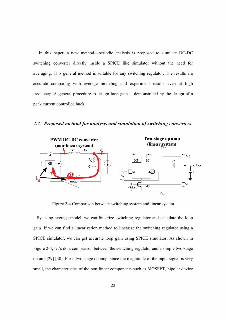
Figure 2-4 Comparison between switching system and linear system ......................................... 22
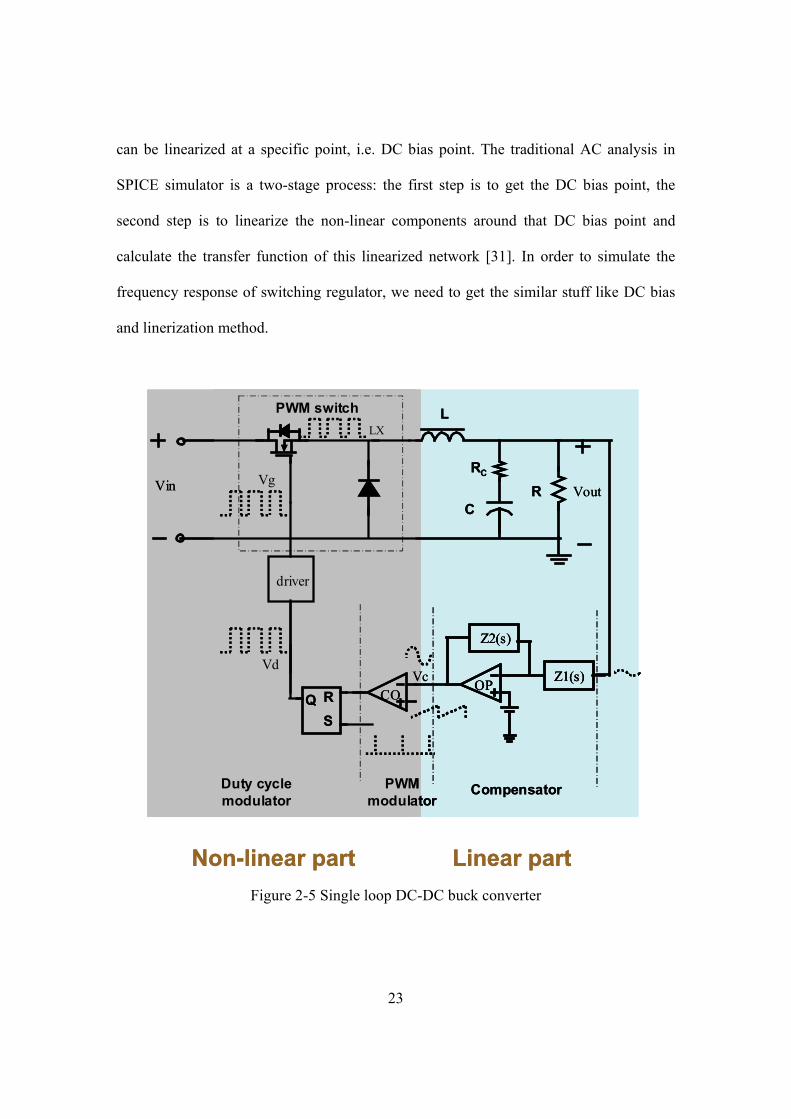
Figure 2-5 Single loop DC-DC buck converter ............................................................................ 23
Figure 2-6 Periodic steady state and new “DC” bias concept ...................................................... 24
Figure 2-7 Frequency spectrum of single loop buck .................................................................... 25
Figure 2-8 Comparison between duty cycle modulator and mixer............................................... 26
Figure 2-9 Periodic analysis and traditional AC analysis............................................................. 29
Figure 2-10. Block diagram of experimental structure................................................................. 32
Figure 2-11 Comparison of control to output transfer function for buck converter between
periodic analysis and average model .................................................................................... 33

xii
Figure 2-12 Small-signal transfer function has minimum points at integral multiples of
switching frequency .............................................................................................................. 35
Figure 2-13 Explanation for the minimum points at integral multiples of switching
frequency............................................................................................................................... 37
Figure 2-14 Comparison of control to output transfer function with current loop closed
for buck converter between Dr. Ridley’s model and periodic analysis ................................ 39
Figure 2-15 Comparison between experiment results and simulation results .............................. 42
Figure 2-16 Loop gain design flow based on periodic method .................................................... 43
Figure 3-1 Inductor current slew rate and output voltage drop .................................................... 47
Figure 3-2 Linear-Non Linear control in [39]............................................................................... 49
Figure 3-3 Block diagram of advanced V2 control ....................................................................... 51
Figure 3-4 Working wave for V2 control...................................................................................... 52
Figure 3-5 Simplified block diagram of peak current control ...................................................... 54
Figure 3-6 Modulation waveform at steady state for different loads............................................ 55
Figure 3-7 Block diagram for the cotangent control..................................................................... 56
Figure 3-8 I-V curve of the cotangent gain block......................................................................... 57
Figure 3-9 Block diagram of cotangent compensator................................................................... 59
Figure 3-10 Cotangent function with different magnitude A ....................................................... 60
Figure 3-11 Cotangent function with different frequency f .......................................................... 61
Figure 3-12 Transfer function of the cotangent compensator....................................................... 63

xiii
Figure 3-13 System loop gain for the cotangent control............................................................... 65
Figure 3-14 Typical system diagram for a switching regulator.................................................... 67
Figure 3-15 Approximation system block diagram for cotangent control.................................... 68
Figure 3-16 Relationship of output of segmented linear function with input signal
amplitude A........................................................................................................................... 69
Figure 3-17 Plot of the describing function plotted against A, the input amplitude to the
nonlinearity ........................................................................................................................... 70
Figure 3-18 Nyquist plot of DF(A) and G(jw).............................................................................. 71
Figure 3-19 Comparison between linear control and cotangent control....................................... 72
Figure 3-20 Comparison between Cotangent control and LnLc control ...................................... 72
Figure 3-21 Comparison between Cotangent control and V2 control........................................... 73
Figure 3-22 Comparison between Cotangent control and traditional bang-bang control............. 74
Figure 3-23 Combination of cotangent control and fast non-linear active clamp control ............ 75
Figure 3-24 Transient response (5V->1.5V, 0.2A load, 1A step) ................................................ 78
Figure 3-25 Transient response from DCM to CCM.................................................................... 79
Figure 3-26 Op-amp based one-zero-two-pole compensator network for peak current
control switching DC-DC converter ..................................................................................... 82
Figure 3-27 Miller effect capacitance booster .............................................................................. 84
Figure 3-28 Negative feedback loop inverse a transfer function.................................................. 85
Figure 3-29 A general compensator structure for peak current control........................................ 86

xiv
Figure 3-30 Simplified system block diagram for peak current control ....................................... 88
Figure 3-31 Control to output transfer function with current loop closed.................................... 89
Figure 3-32 Simplified block diagram for peak current control boost converter ......................... 91
Figure 3-33 Transfer function Goc changes for different application cases .................................. 93
Figure 3-34 Transfer function Goc with constant ripple assumption............................................. 94
Figure 3-35 Adaptive compensation concept ............................................................................... 96
Figure 3-36 System loop gain with adaptive compensation ......................................................... 97
Figure 4-1 Cross-section of NLDMOS used in the chip............................................................. 101
Figure 4-2 Parasitic components simulation by ISETM for NLDMOS with w=100u................. 103
Figure 4-3 Breakdown voltage simulation by ISETM for NLDMOS with w=100u, L=0.5u ...... 104
Figure 4-4 Needed SOA for power switches .............................................................................. 105
Figure 4-5 Measured SOA for different layout structure [51].................................................... 106
Figure 4-6 Efficiency breakdown for 1.5MHz and 2MHz ......................................................... 107
Figure 4-7 Conventional gate drive (CGD) ................................................................................ 109
Figure 4-8 Resonant gate drive ................................................................................................... 109
Figure 4-9 Timing diagram for the high-speed driver ................................................................ 111
Figure 4-10 Simple modeling of switching behavior ................................................................. 112
Figure 4-11 Proposed multi-stage gate drive (MSGD)............................................................... 114
Figure 4-12 Simplified block diagram of MSGD....................................................................... 115

xv
Figure 4-13 Comparison between CGD and MSGD .................................................................. 116
Figure 4-14 MSDG can obtain adaptive dead time control ........................................................ 117
Figure 4-15 Control signal change with load current ................................................................. 118
Figure 4-16 Simplified block diagram of burst mode................................................................. 119
Figure 4-17 Comparison between DCM mode and burst mode ................................................. 120
Figure 4-18 External resistor current sensing ............................................................................. 121
Figure 4-19 Rds_on current sensing ........................................................................................... 122
Figure 4-20 Traditional RC current sensing ............................................................................... 122
Figure 4-21 Signal noise ratio is too small for traditional RC current sensor ............................ 123
Figure 4-22 New lossless RC sensor structure (1)...................................................................... 125
Figure 4-23 Design equations for new RC sensor structure (1).................................................. 125
Figure 4-24 New lossless RC sensor structure (2)...................................................................... 126
Figure 4-25 Design equations for new RC sensor structure (2).................................................. 126
Figure 4-26 Comparison between the new RC sensor and traditional RC sensor ...................... 127
Figure 4-27 Modeling parameters for the new sensor ................................................................ 127
Figure 4-28 Modeling of the new RC sensor.............................................................................. 128
Figure 4-29 Results of the modeled sensor................................................................................. 129
Figure 5-1 Simplified diagram of a peak current control buck................................................... 132
Figure 5-2 Pin configuration of the developed chip ................................................................... 133

xvi
Figure 5-3 Typical application of the developed chip ................................................................ 134
Figure 5-4 Detail structure of the whole chip ............................................................................. 136
Figure 5-5 Test bench for the developed chip ............................................................................ 138
Figure 5-6 Tested power on start up when Vin=3V, Vout=1.5V Iload=200mA.............................. 139
Figure 5-7 Tested waveform for high input voltage ................................................................... 140
Figure 5-8 Tested waveform for low input voltage .................................................................... 141
Figure 5-9 Tested waveform for DCM operation ....................................................................... 142
Figure 5-10 Tested waveform for transient response with low input voltage ............................ 143
Figure 5-11 Tested waveform for transient response with high input voltage ........................... 144
Figure 5-12 Efficiency Vs load current at Vin=5V, Vout=1.5V.................................................... 145
Figure 5-13 Loss break down at Vin=5, Vout=1.5 and Iload=0.4A................................................. 146

xvii
Table 2-1 Parameters for the experimental structure.................................................................... 32
Table 4-1 MAIN PARAMETERS FOR POWER DEVICES .................................................................... 102
Table 5-1 Pin configuration of the developed chip..................................................................... 134
Table 5-2 Specifications of the developed chip.......................................................................... 135

1
Chapter 1: Introduction
1.1. Background
Cell phone
MP3 player
PDA
DVD Player
Laptop
Cell phoneCell phone
MP3 playerMP3
player
PDAPDA
DVD Player
Laptop
PDAPDAPDA
Figure 1-1 Power management IC is widely used [1]
The earth is mobile [1]. As shown in Figure 1-1, we are using different kinds of
electronic devices in our everyday life. Any electronic device needs an energy source ⎯
electrical power. In order to provide a high quality power source for electronic devices,
power management devices are needed. Power management is naturally a basic part for
almost all of the electronic devices. Traditional power management devices are mostly
built by discrete components on a PCB board. The profile of the power management part
is normally big and the design is relatively complex. With the development of
microelectronics, more and more power management solutions are replaced with power
management ICs. A power management IC can be only a controller IC, one
semiconductor power switch or a combination of these parts even with energy storage
device like inductor and capacitor resonant tank. By integrating the parts together into a

2
tiny chip, the size of the whole power management park is much smaller and the design
can be much easier. As shown in the right part of Figure 1-1, if we take a close look into
a tiny PDA device, we will see bunch of power management ICs inside this equipment
serving different parts. With the electronic equipments becoming more and more
complicated, the requirements for power management are more and more strict. Even for
a small part of the tiny electronic device, a dedicated power management IC may be
needed to serve it, which induce a huge market for power management ICs [6][7] [8]. As
we know, there are a lot of big companies such as Analog Device, National
semiconductor, Texas Instruments, Maxim etc working in power management IC market.
As predicted in Figure 1-2, there is almost 7,000,000,000 dollars market for power
management ICs until 2006 [9]. This market is going to keep growing because more and
more new electronic devices are coming into our life.
Ref: http://www.vdc-corp.com/power/annual/03/br03-14exhibits.html#vol1Ref: http://www.vdc-corp.com/power/annual/03/br03-14exhibits.html#vol1
Figure 1-2 Shipment forecast for power supply and power management ICs

3
1.2. Trends of the modern power management IC
Accompanying with this market growth, some new trends and challenges for power
management ICs rise up. In order to save power, the power supply voltage of the
electrical device should be reduced according to equation VIP ×= . So the output
voltage of power management device drops lower and lower from 5V to 3.3V, and even
to 1.8V or below 1V for VRD application in desktop computer [10][11]. At the same
time, the output current is going higher and higher because the digital logic circuitry in
electronic device are more and more complicated, which consumes a lot of current; As
we know, most of the digital circuitry generates pulsating current spike, which causes a
high requirements for transient response of power management device. However, the
tolerance window of the output voltage is going smaller and smaller because of the strict
requirements from the fancy devices used in modern electronic products.
In a word, efficient performance, high functionality, smart protection, small profile,
fast transient and low cost are the most wanted features for modern power management
ICs, especially for mobile power since the energy source of potable device are batteries
[12]. The capacity of battery is very limited at most of the case and some batteries are
quite expensive. Nobody would like to waste a lot of money on power management
device due to its poor performence.

4
Volterra VRM10CPES
monolithic VRM (fs=4MHz)
iPOWIR from IR
Monolithic DC-DC
converter with spiral inductor
(fs=5MHz)
Discrete solution Integrated driver & power device
Integrated driver, power device,control core
All in one
Volterra VRM10Volterra VRM10CPES
monolithic VRM (fs=4MHz)
CPES monolithic
VRM (fs=4MHz)iPOWIR from
IRiPOWIR from
IR
Monolithic DC-DC
converter with spiral inductor
(fs=5MHz)
Monolithic DC-DC
converter with spiral inductor
(fs=5MHz)
Discrete solution Integrated driver & power device
Integrated driver, power device,control core
All in one
(a) (b) (c) (d)
Figure 1-3 Monolithic integration development process
In order to reduce profile, the number of external components should be as small as
possible, which means that compensator, ramp compensation, current sensor, driver and
even power devices should be all implemented on a single chip, i.e. monolithic
integration. Since it is difficult to integrate large size and high Q value inductor and large
value capacitor on silicon, most of the power management ICs will not integrate energy
storage device on silicon [13]. Future development will even make it possible to integrate
the energy storage elements, such as the inductor and capacitor. This development relies
on further technology development in the area of high-density inductor and capacitor
design that is compatible with semiconductor technology, as well as the techniques to
operate the converter at extremely high frequencies, such as 100 MHz[3][2][18]. Figure
1-3 shows the comparison between the discrete and monolithic solution. As shown in
Figure 1-3 (a), this device is mainly composed of discrete parts such as controller, driver,
power switches and passive components [14]. The designer has to build controller,
compensator and even logic components by himself. In 2000, Internal Rectifier TM release
iPOWIR product series as shown in Figure 1-3(b) [15]. The driver is packaged with
power switches together. The designer needs only to put this integrated power stage with

5
one controller to build a switching converter. It simplifies the design a lot. At the mean
time, by doing this, the efficiency is improved several percent and noise generated by
switching is reduced a lot due to the reduced parasitic components. This kind of
integration mode is becoming the dominant solution for VRD application now and in the
near future [16]. Figure 1-3 (c) is a monolithic two-channel VRM designed by Nick Sun
from CPES Virginia Tech [2]. In this chip, the controller, logic, driver and even power
switches are integrated on single silicon. The designer needs only to add a resonant tank
externally to build a switching converter. The whole converter is very small and quite
simple. At the same time, it removes all of the parasitic inductance between controller
and driver, driver and power switches, which reduces a lot of noise and voltage spike
generated by the parasitic inductance and improves the efficiency a lot. This is the
monolithic solution that this work will focus on mostly. Figure 1-3 (d) is a thin film
inductor based 5MHz switching DC-DC converter developed by Katayama, Y in [3].
Since the switching frequency is almost 5MHz, a relative small inductor is needed in this
switching converter. It is possible to integrate a small inductor like this on silicon using
the spiral inductor. However, the Q value of this thin film inductor is relative low, which
cause a lot of power loss in this inductor and lower down the efficiency a lot. Since the
switching frequency is very high, it will induce a lot of switching loss too. The energy
storage components inductor and capacitor occupy a lot of chip area as we can see from
Figure 1-3 (d). All of these disadvantages make this “true monolithic integration”
solution unacceptable in the reality using current technology.
Figure 1-4 shows the typical structure of a peak current controlled switching buck
regulator. The whole converter can be divided into the following several parts: feedback

6
generation and compensator, PWM modulator, control logic generation, dead-time
control, current sensor, driver, power switches and energy storage resonant tank. For
synchronous buck, a transistor replaces the rectifier diode in order to reduce conduction
loss. The basic principle of this control scheme is that: when output voltage drops down,
feedback signal will be lower than the reference voltage Vref. Error amplifier will amplify
this difference between feedback signal and reference voltage. The output of the error
amplifier, i.e. control signal Vc will rise up. Vc will compare with a saw-tooth signal and
generate a larger duty cycle clock. This clock signal will combine with some protection
signals like over voltage protection, over current protection etc to generate a PWM signal.
The driver block will pass this PWM signal to the gate of power switch and drive the
power switch to control the transferred energy. Since duty cycle is larger, more energy
will be transferred to the output capacitor C and output voltage will rise up until it is
higher than reference voltage. The same phenomena will happen when output voltage is
higher than reference voltage. As we can see from Figure 1-4, there is a control loop in
this simplified buck regulator. In order to guarantee a stable and high quality output
voltage, the control loop should be stable, which means that there should be some phase
margin and gain margin for this control loop. The voltage controlled buck regulator has a
similar structure except there is no current sensor in this diagram. In this work, we will
focus on the monolithic structure shown inside the dot-line box. In this monolithic
structure, all of the components are on a single chip except the energy storage elements
such as inductor L and capacitor C.

7
driver
OP Z1(s)
Z2(s)
Vc
Vin Vout
RS
Q
LX
Compensator
PWM modulator
L
CR
RC
Vd
Vg
CS
COVref
driver
OP Z1(s)
Z2(s)
Vc
Vin Vout
RS
Q RS
Q
LX
Compensator
PWM modulator
L
CR
RC
Vd
Vg
CS
CS
COCOVref
Figure 1-4 Monolithic structure focused on in this work
Besides monolithic integration, high switching frequency is another trend for power
management IC [17]. Ten years ago, KHz may be a high frequency for switching
regulators. Now, people are talking about several hundred kHz and even MHz switching
frequency. There are some products that have a very high switching frequency like
2MHz, 4MHz. With the electronic products becoming smaller and smaller, the power
management devices are needed to be smaller and smaller. The bulky part of switching
regulator is energy storage components like inductor and capacitor. By using high
switching frequency, small size inductor and capacitor can be used, which will reduce the
size of the whole power management device a lot. At the mean time, high switch
frequency will improve the transient response due to its potential higher bandwidth. All

8
of these benefits make high switching frequency an obvious trend for modern power
switching regulator.
In the following two sections, we will discuss the advantages and challenges for
monolithic integration and high switching frequency.
1.2.1. Advantages and challenges for monolithic integration
Comparing with discrete switching DC-DC converter, monolithic integration brings a
number of benefits: The number of external components can be reduced to only the main
inductor and output capacitor so the power density can be increased drastically; which is
very important for modern electronic devices. The parasitic components such as bond
wire inductance, trace resistance are reduced, which is important for high frequency and
noise sensitive applications [2]; With everything packaged together, the end user can plug
this kind of module into the whole system easily, which simplifies the design and
improve the reliability of the whole system
Besides the advantages, monolithic integration brings some new design challenges;
one chip to multi-market is a common case in industry, which means that wide input,
output voltage and load current range are possible for a single chip. Since compensator,
ramp compensation and current sensor are integrated inside chip, how to design the
compensator to stabilize the system for wide input and output ranges is a big challenge.
Since power devices and drivers are integrated with control circuit, there is a nature path
⎯ substrate between the power stage and control part. Noise can be easily injected from
power stage to analog control part and affect the correct functionality of the noise
sensitive analog circuitry in the control part. How to provide noise separation between
power stage and control part is a design challenge for monolithic integration; Since the

9
battery source for portable power can be a single 1.2V nickel metal hydride with a final
discharge voltage of 0.8V to several 4.3V LiIon batteries in series [1], both low-voltage
and high-voltage operation may be required for portable power ICs. At the low-voltage
end, low-voltage analog IC design is a challenge. At the high-voltage end, higher-voltage
CMOS or CMOS variants are needed for high-input-voltage applications. How to
combine the high voltage device and low voltage device on the same silicon and provide
a good protection for all devices is another design challenge. It is well known that large
size passive components like resistors and capacitors will take a lot of silicon area.
Compensator used in a switching DC-DC converter may need a passive impedance
network to generate a low frequency pole or zero. On-chip compensator implementation
may take a lot of silicon area, especially if a low frequency zero is needed like peak
current control switching converter. How to implement a good compensation network on
silicon using smallest silicon area is another challenge for monolithic power management
IC design. All of these challenges make the monolithic integration a hard topic. In
chapter 2, 3 and 4 of this work, some new ideas are proposed to solve some of these
design issues.
1.2.2. Advantages and challenges for high frequency design
As discussed above, high switching frequency is another trend for modern power
management ICs. Comparing with low frequency switching DC-DC converter, high
frequency brings a number of benefits and new challenges. In the practice, the bandwidth
of the control loop is designed to be around 1/10 or 1/5 of the switching frequency, which
means that high switching frequency will generate a potential higher bandwidth. As

10
shown in Figure 1-5 [20], the relationship between the inductor current rising slew-rate
and bandwidth is shown in equation (1-1).
2πωco
r
o
avg
ItI
dtdi ⋅Δ
=Δ
= (1-1)
From equation (1-1), we can see that, with higher bandwidth, the inductor current will
goes to the steady state value faster and keep the output voltage from dropping further.
Higher switching frequency will generate faster transient response during load current step-
up or step-down transient. That is very important for modern power management ICs.
High switching frequency can also reduce the size of energy storage elements and
increase the power density. With Mhz switching frequency, the inductor size can be
dropped down to several hundred nH and output capacitor can be several uF, which will
reduce the profile of the whole power management device a lot. With the switching
frequency increasing further, the inductor and capacitor size will drop down further to tens
nH and pF so that they can be monolithically integrated on the same silicon with controller
and power switch [18].
Another benefit of high switching frequency is that it can reduce the compensation cost a
lot. According to Dr. Ridley’s model [22], the dominant pole of the control-to-output
transfer function with current loop closed is
)5.0'(1−⋅⋅
⋅+
⋅≅ Dm
CLT
CR cs
pdomω (1-2)
With reduced energy storage elements L and C, ωpdom is going to be at higher frequency.
Only a high frequency zero is needed for the compensation. Comparing with low

11
frequency zero, much smaller resistor and capacitor are needed to generate the high
frequency zero. Since it is very difficult to implement high value passive components on
silicon, high switching frequency will reduce a lot of the silicon area and save cost.
With high switching frequency, the output ripple and inductor current ripple can be
very small. It is good when the output voltage is already very low like 1V for some
special application such as VRD for desktop [19].
iL L
GD
rC
C
rL
comp
io
ωc
iL L
GD
rC
C
rL
comp
io
ωc
2πωco
r
o
avg
ItI
dtdi ⋅Δ
=Δ
=
tr iLΔIo
tr iLΔIo
tr iLΔIo
Figure 1-5 Relationship between bandwidth and transient response [20]
Besides the benefits, high switching frequency brings a lot of new design issues too;
with the switching frequency going higher and higher, the switching period is going to
drop down like 250ns when switching frequency is 4MHz. However, the delay of a very
fast comparator is around 10ns, the delay of a fast driver is around 10ns. The sum of all
of the delay around the control loop can be around 40ns to 50ns. This delay is around 1/5
of the switching period and not negligible. From the frequency domain point view, this
delay will cause some phase drop in the control loop and make the control loop unstable.
All of these require the design of a very fast control loop and an accurate control loop

12
modeling. The modeling method based on the state space averaging cannot accurately
model this kind of parasitic effects since it uses a lot of ideal components like ideal op
amp, comparator, driver and even power switch. There is no delay or accurate delay for
these blocks used in the model. How to get the accurate loop gain of the control loop for
the high frequency switching converter is a fundamental issue for high frequency design;
In order to reduce the phase drop, high-speed circuit is needed for the blocks in the
control loop. It causes some design challenges for the circuit designer.
When switching frequency goes high, the switching loss will rise up. In order to reduce
switching loss, the power switches should be turned on and off very fast; the parasitic
inductance will generate some voltage spike on the power devices, which requires a
better performance of the power switches and a good isolation between the power stage
part and analog control part. At the mean time, dead-time control becomes a critical issue
since the switching period is much smaller at high switching frequency. Normally, the
dead time of the driver is around 20ns for turn-on and totally around 50ns for the whole
switching period, which is around 1/5 of the switching period when the switching period
is 4MHz. The benefit of the synchronous device to increase efficiency is almost gone.
The body diode of the synchronous device will consume a lot of power and lower down
the efficiency a lot.
Since the voltage spike at the switching node can be much larger at high switching
frequency, current sensing becomes even more challenging comparing with the low
frequency counterparts. The speed of the current sensor needs to be fast, the common
mode rejection ratio (CMRR) of the input circuit for the current sensor needs to be much
higher. All of these make it very difficult to get an accurate current sensing [21].
13
As mentioned before, one chip to multi-market is a common practice in industry.
Normally, a power management IC could have a wide load range such as 0-1.5A. How to
keep high efficiency for the whole working range is another issue for monolithic high
frequency switching DC-DC converter.
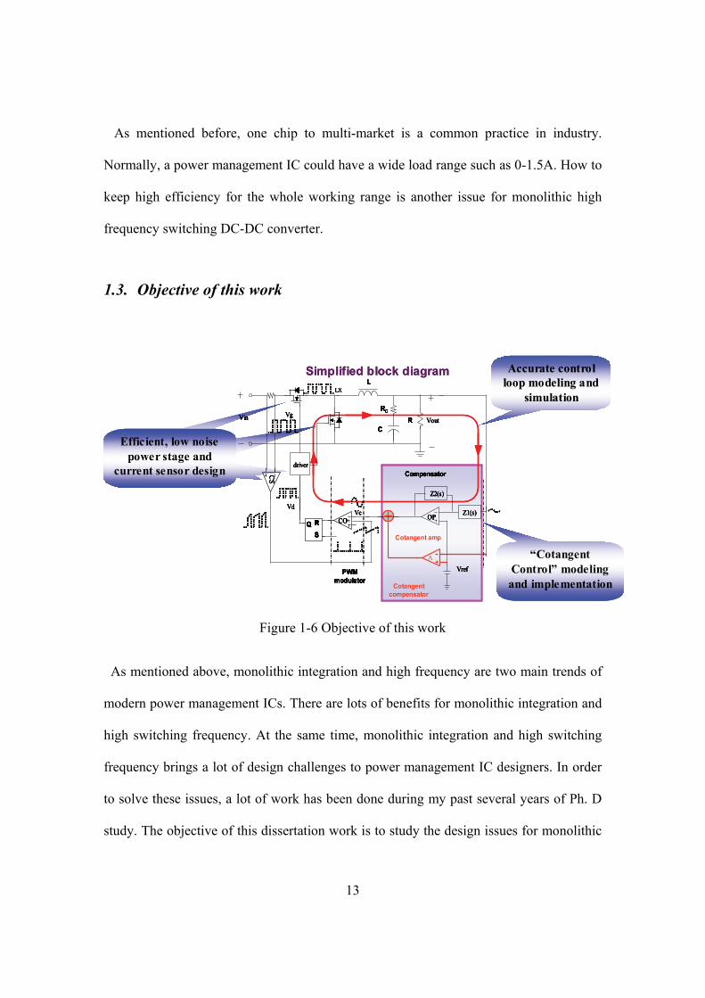
1.3. Objective of this work
A
Cotangent amp
Cotangent compensator
A
Cotangent amp
Cotangent compensator
“Cotangent Control” modeling and implementation
A
Cotangent amp
Cotangent compensator
A
Cotangent amp
Cotangent compensator
“Cotangent Control” modeling and implementation
Efficient, low noise power stage and
current sensor design
Efficient, low noise power stage and
current sensor design
Efficient, low noise power stage and
current sensor design
Efficient, low noise power stage and
current sensor design
Efficient, low noise power stage and
current sensor design
Efficient, low noise power stage and
current sensor design
Efficient, low noise power stage and
current sensor design
Efficient, low noise power stage and
current sensor design
Accurate control loop modeling and
simulation
Accurate control loop modeling and
simulation
driver
OP Z1(s)
Z2(s)
Vc
Vin Vout
RS
Q
LX
Compensator
PWM modulator
L
CR
RC
Vd
Vg
CS
CO
Vref
driver
OP Z1(s)
Z2(s)
Vc
Vin Vout
RS
Q RS
Q
LX
Compensator
PWM modulator
L
CR
RC
Vd
Vg
CS
CS
COCO
Vref
Simplified block diagram
driver
OP Z1(s)
Z2(s)
Vc
Vin Vout
RS
Q
LX
Compensator
PWM modulator
L
CR
RC
Vd
Vg
CS
CO
Vref
driver
OP Z1(s)
Z2(s)
Vc
Vin Vout
RS
Q RS
Q
LX
Compensator
PWM modulator
L
CR
RC
Vd
Vg
CS
CS
COCO
Vref
Simplified block diagram
Figure 1-6 Objective of this work
As mentioned above, monolithic integration and high frequency are two main trends of
modern power management ICs. There are lots of benefits for monolithic integration and
high switching frequency. At the same time, monolithic integration and high switching
frequency brings a lot of design challenges to power management IC designers. In order
to solve these issues, a lot of work has been done during my past several years of Ph. D
study. The objective of this dissertation work is to study the design issues for monolithic

14
integration of high frequency switching DC-DC converter. The whole research work can
be divided into the following three parts.
Stability is the fundamental requirement for a switching converter ASIC. Achieving
this requires an accurate loop gain design, especially for high speed switching converter
because of the parasitic delay. Traditional average model ignores those parasitic delay
and cause the difference between modeling results and real circuitry. Parasitic delay is
difficult to be estimated except by simulation. However, since DC-DC switching
converters are time-varying system, traditional small signal analysis ⎯ AC analysis in
SPICE cannot be directly used to simulate the loop gain of this kind of system. It caused
a lot of trouble for power management IC designer. In this work, a new accurate method
⎯ Periodic analysis based method is proposed to analyze and simulate DC-DC switching
converter inside a SPICE like simulator without the need for averaging [5]. This general
method is suitable for any switching regulators. The modeling results for buck are
presented. The results are accurate comparing with average modeling and experimental
results even at high frequency part. A general procedure to design loop gain based on
SPICE simulator is proposed.
Compensator is a key part in the control loop of switching regulator. It determines the
stability, transient response and even loop delay. Since compensator needs some low
frequency zeros or poles, some large value passive components such as resistors and
capacitors are needed in the compensator implementation [22]. For monolithic
integration, compensator is integrated on silicon. It will take a lot of silicon area to build
large value resistor and capacitor on silicon. In order to address all these design issues,
several novel design concepts are proposed for monolithic integration of high frequency

15
switching DC-DC converter; a novel control scheme ⎯ Cotangent Control (Ctg control)
is proposed for fast transient response; In order to realize on-chip implementation of the
compensator, especially for low frequency zero, active feedback compensator is
developed and a general design procedure is proposed. Adaptive compensation is
proposed to stabilize the whole system for a wide application range. The final purpose of
all of these concepts is to get a good stability at all kinds of application cases and a fast
transient response with smallest cost.
Power stage is another key part for switching converter. It determines the efficiency,
reliability, noise and ripple etc. Another important issue related with power stage is
current sensing. For high speed switching converter, current sensing is becoming more
and more difficult. In this work, a multi-stage driver and multi-section device concepts
are investigated for high efficiency and low noise power stage design. And finally, a new
noise insensitive lossless RC sensor is proposed for high speed current sensing.
In order to verify all of these design concepts, a high frequency, wide input range
monolithic buck converter ASIC with fast transient response is designed based on
advanced trench BCD technology. Some experimental results are presented to verify the
control concepts.
1.4. Outline of the dissertation
The whole dissertation is divided into the following six chapters.
Chapter 1 is the literature review of the background for monolithic integration and high
frequency design. The benefits and design challenges of monolithic integration and high

16
frequency design are introduced, which comes out the objective of this work; and finally
the outline structure of the dissertation.
Chapter 2 discussed the modeling issue for high frequency switching converter. In order
to solve this design issues, a novel periodic small signal analysis based method for
frequency response modeling and simulation in SPICE is proposed. The basic concepts
are introduced first. The development of the method is discussed. A brief review of the
algorithms for Periodic Steady State (PSS) and Periodic AC (PAC) analysis is followed.
Then, a comparison between the new method, averaging model and experimental results
are discussed to verify the new method. Finally, a general design procedure for the loop
gain design based on SPICE is summarized at the end of this chapter.
Chapter 3 discussed the cotangent control modeling and implementation. First, the review
of basic concepts for control loop modeling, compensator design and transient response
mechanism is done. After that, the development of Cotangent Control (Ctg control) is
discussed. Then, active feedback compensator concept is proposed. The general
implementation of active feedback compensator is derived and discussed. After this,
Adaptive compensation concept is derived and discussed based on peak current control.
Chapter 4 discussed the design of efficient, low noise power stage and current sensing.
First, multi-stage driver and multi-section device concepts are investigated for high
efficiency and low noise power stage design. Then a noise insensitive lossless RC sensor
is proposed for high speed current sensing.

17
Chapter 5 discussed the experimental results. First, the high level introduction of the
system structure of the whole chip is done. The pin configuration and pin description are
described. The specification of the experimental chip is introduced. The typical
application circuit is discussed. And finally, the details of the whole system structure are
discussed. Some experimental results are presented after that to verify the functionality of
the silicon.
Chapter 6 is the summary of this work and some future work to do.

18
Chapter 2: Accurate Control Loop Modeling and Simulation
2.1. Introduction
Average model
driver
OP Z1(s)
Z2(s)
Vc
Vin Vout
RS
Q
LX
Compensator
PWM modulator
L
CR
RC
Vd
Vg
CS
COVref
driver
OP Z1(s)
Z2(s)
Vc
Vin Vout
RS
Q RS
Q
LX
Compensator
PWM modulator
L
CR
RC
Vd
Vg
CS
CS
COCOVref
Figure 2-1 Linerization of switching converter using average model
Stability is the fundamental requirement in designing switching converter ASIC.
Achieving this requires an accurate loop gain modeling or simulation. As we know, some
of the parts such as power switch, PWM modulator in a switching regulator are working
in large signal mode. The whole converter system is a time varying system. Traditional
classic control theory applies only to linear system. In order to model switching regulator,
the first step is to linearize the whole system. How to linearize a switching regulator

19
system was a tough topic in power electronics before 1960’s. Average model was
proposed around 1970’s and applied to switching regulator system
successfully[23][24][25].
Figure 2-1 is a typical peak current controlled switching regulator system. These two
power switches are replaced by average model in order to linerize the system. Duty cycle
is introduced in the modeling. By using the average model, the transfer function from
duty cycle to output voltage and all other transfer functions can be derived. By including
the other linear part, we can easily get the loop gain and phase margin of the control loop.
Since the whole system is a linear network now, traditional classic control theory can be
used on this kind of system to design control loop. Figure 2-2 is the system block
diagram using average model for peak current controlled system [22]. In real design, the
system block diagram shown in Figure 2-2 can be simplified to the system block diagram
shown in Figure 2-3 as one-order system.
Gv
Gdi
Gdv
Fm
-Hi
He
Gi
Kf -Hv
Kr
Vin Vout
dTv
Ti
Vc
iL
Gv
Gdi
Gdv
Fm
-Hi
He
Gi
Kf -Hv
Kr
Vin Vout
dTv
Ti
Vc
iL
Figure 2-2 System block diagram of voltage controlled buck using average model

20
Gv
Gdi
Gdv
Fm
-Hi
He
-Hv
Vin Vout
dTv
Ti
Vc
iL
Gv
Gdi
Gdv
Fm
-Hi
He
-Hv
Vin Vout
dTv
Ti
Vc
iL
Figure 2-3 Simplified system block diagram of peak current controlled buck
During the modeling shown above, some ideal assumptions are made. The delay of the
comparator, driver are ignored. These delays are not negligible in high switching
frequency regulator since the switching period is too short and the delay is comparable
with the switching cycle. The phase drop caused by those delay is not negligible and
needed to be considered during modeling.
Though averaging model is a good tool to analyze the low frequency characteristics of
switching regulator, it is not accurate enough at some cases, especially for high switching
frequency regulator. Simulation may be the only method to get the accurate control loop
gain at this case. However, since switching regulator is a non-linear system, there is no
good method to simulate accurate loop gain of this kind of non-linear system. Most
numerical methods in SPICE are developed for linear circuit. In traditional AC analysis,
SPICE simulator linearizes circuit around a DC point and calculates the small signal
response of the circuit around that DC bias point. Since DC-DC switching converters are

21
mixed-signal time-varying system, some circuit blocks in the converter like PWM
modulator, driver, switches and diodes are non-linear and working in large signal mode,
traditional small signal analysis in SPICE cannot be directly used to simulate the loop
gain of this kind of system. This causes a lot of trouble in converter design, especially if
one is doing power management IC design. In recent years, some methods were proposed
to simulate DC-DC switching converters. James Groves proposed a periodic operating
trajectory concept and developed a simulation tool for the frequency analysis of DC-DC
switching converters[26]. In [4], Richard P.E. Tymerski developed “PWM switch”
concept and proposed large signal and small signal model for “PWM switch”. In [27],
“software network analysizer” method is proposed using MATLABTM and PSPICE to
simulate loop gain by frequency sweep. SIMPLISTM may be the best software on the
market that can be used to simulate loop-gain of DC-DC converter directly. However, the
model in SIMPLISTM is piece-wise linear model. It doesn’t work for SPICE model [28].
None of these methods can be directly used for SPICE like simulator, which causes a lot
of trouble for power management ASIC designers. The normal approach to design a DC-
DC switching converter ASIC in industry is to do modeling first by MATHCADTM or
MATLABTM, then design the transistor level circuit to match modeling results. Since a
lot of ideal assumptions are made in modeling, modeling results may not be close to real
circuit. For example, modeling can’t take into account the delay in real circuit, which
may cause some additional phase drop. If a method can be directly used to simulate the
loop gain of switching converters by SPICE like simulator, ASIC designers can use it to
get accurate loop gain that takes care of all the delay and non-linear effect at transistor
circuit level.
22
In this paper, a new method—periodic analysis is proposed to simulate DC-DC
switching converter directly inside a SPICE like simulator without the need for
averaging. This general method is suitable for any switching regulator. The results are
accurate comparing with average modeling and experiment results even at high
frequency. A general procedure to design loop gain is demonstrated by the design of a
peak current controlled buck.
2.2. Proposed method for analysis and simulation of switching converters
iL L
GD
rC
C
rL
comp
io
ωctd
PWM DC-DC converter (non-linear system)
iL L
GD
rC
C
rL
comp
io
ωctd
iL L
GD
rC
C
rL
comp
io
ωc
iL L
GD
rC
C
rL
comp
io
ωctd
PWM DC-DC converter (non-linear system)
Two-stage op amp (linear system)
Two-stage op amp (linear system)
Figure 2-4 Comparison between switching system and linear system
By using average model, we can linearize switching regulator and calculate the loop
gain. If we can find a linearization method to linearize the switching regulator using a
SPICE simulator, we can get accurate loop gain using SPICE simulator. As shown in
Figure 2-4, let’s do a comparison between the switching regulator and a simple two-stage
op amp[29] [30]. For a two-stage op amp, since the magnitude of the input signal is very
small, the characteristics of the non-linear components such as MOSFET, bipolar device
23
can be linearized at a specific point, i.e. DC bias point. The traditional AC analysis in
SPICE simulator is a two-stage process: the first step is to get the DC bias point, the
second step is to linearize the non-linear components around that DC bias point and
calculate the transfer function of this linearized network [31]. In order to simulate the
frequency response of switching regulator, we need to get the similar stuff like DC bias
and linerization method.
driver
COOP Z1(s)
Z2(s)
Vc
Vin Vout
RS
Q
LX
CompensatorPWM modulator
PWM switch L
CR
Duty cycle modulator
RC
Vd
Vg
driver
COCOOP Z1(s)
Z2(s)
OP Z1(s)
Z2(s)
Vc
Vin Vout
RS
Q RS
Q
LX
CompensatorPWM modulator
PWM switch L
CR
Duty cycle modulator
RC
Vd
Vg
Non-linear part Linear part
driver
COOP Z1(s)
Z2(s)
Vc
Vin Vout
RS
Q
LX
CompensatorPWM modulator
PWM switch L
CR
Duty cycle modulator
RC
Vd
Vg
driver
COCOOP Z1(s)
Z2(s)
OP Z1(s)
Z2(s)
Vc
Vin Vout
RS
Q RS
Q
LX
CompensatorPWM modulator
PWM switch L
CR
Duty cycle modulator
RC
Vd
Vg
driver
COOP Z1(s)
Z2(s)
Vc
Vin Vout
RS
Q
LX
CompensatorPWM modulator
PWM switch L
CR
Duty cycle modulator
RC
Vd
Vg
driver
COCOOP Z1(s)
Z2(s)
OP Z1(s)
Z2(s)
Vc
Vin Vout
RS
Q RS
Q
LX
CompensatorPWM modulator
PWM switch L
CR
Duty cycle modulator
RC
Vd
Vg
Non-linear part Linear part
Figure 2-5 Single loop DC-DC buck converter

24
Vc
Vout
Vg
Il
VC
VG
IL
VOUT
Vc
Vout
Vg
Il
Vc
Vout
Vg
Vc
Vout
VgVg
Il
VC
VG
IL
VOUT
VC
VG
IL
VOUT
Figure 2-6 Periodic steady state and new “DC” bias concept
Figure 2-5 is a typical single loop PWM DC-DC converter. Most of the blocks in this
system are linear except switches, PWM modulator and drivers. As shown in Figure 2-6,
if we take a closer look at the detail waveform at every node in this system, we will find
that the whole system is working in a periodic steady state with some perturbation. VOUT,
VC, VG, IL are the DC components. Vout, Vc, Vg, Il are the real signals. If we choose the
periodic steady state as a new “DC bias” point, then the system acts like a “linear”
system. The whole system can be linearized around the periodic steady state point; the
periodic small signal analysis can be used to get the frequency response of the switching
converter system. That is the basic concept of “periodic method” proposed in this work.

25
Duty cycle modulatorDuty cycle modulator
Vg(jω)
ω
ω
Vd(jω)
ωs−ωs ωcωc
Vd(jω)
ωωc
LX(jω)
ωs−ωsωcωc
Vout(jω)
ωcωc
Vg(jω)
ω
ω
Vd(jω)
ωs−ωs ωcωc
Vd(jω)
ωωc
LX(jω)
ωs−ωsωcωc
Vout(jω)
ωcωcω
ω
Vd(jω)
ωs−ωs ωcωc ω
Vd(jω)
ωs−ωs ωcωc
Vd(jω)
ωs−ωs ωcωc
Vd(jω)
ωs−ωs ωcωc
Vd(jω)
ωωc
Vd(jω)
ωωc
LX(jω)
ωs−ωsωcωc
LX(jω)
ωs−ωsωcωc
Vout(jω)
ωcωc
Vout(jω)
ωcωc
Vc(t)
Vd(t)
Vg(t)LX(t)
LPFVout(t)
PWM modulator
PWM switch
Vc(t)
Vd(t)
Vg(t)LX(t)
LPFVout(t)
PWM modulator
PWM switch
Vd(t)
Vg(t)LX(t)
LPFVout(t)
PWM modulator
PWM switch
Vg(t)LX(t)
LPFVout(t)
PWM modulator
Vg(t)LX(t)
LPFVout(t)
PWM modulator
LX(t)LPF
Vout(t)
PWM modulator
PWM switch
Figure 2-7 Frequency spectrum of single loop buck
Figure 2-7 is the corresponding frequency spectrum of the signals at different nodes
around the control loop. We can see that: PWM modulator works like a “phase”
modulator except the “phase” is duty cycle. Driver works like a power amplifier.
Switches work like a “phase” demodulator or a square wave sampler. If we consider
PWM modulator, driver and PWM switch as one non-linear block, it looks like a “phase”
modem. The DC gain of this block is pg VV / from Vc to Vout and D(t) from Vg to Vout as
shown in Figure 2-8 (a). We call it “duty cycle modulator”. If we compare “duty cycle

26
modulator” with a mixer as shown in Figure 2-8 (b), we will see that they are quite
similar. Now come to the point, is it possible to use the similar analytic method as that
used for mixer to analyze “duty cycle modulator”? The answer is “yes”. From Figure 2-7,
we can also see that, although PWM modulator, driver and PWM switch will generate
high frequency harmonics, only if these harmonics are higher than 0.5fs, otherwise there
will be no aliasing and output low pass filter will filter them out finally. We only need to
consider the fundamental frequency signal, i.e. “0” sideband signal in periodic small
signal analysis when only loop gain is considered. The loop gain will be the products of
“0” sideband small signal gain of every block around control loop. The same conclusion
can be applied for any switching converter.
Duty cycle modulator
Vg(t) Vout(t)
Vc(t)p
g
VV
)(tD
Duty cycle modulator
Vg(t) Vout(t)
Vc(t)p
g
VV
)(tD
SRF Sbase
LO
SRF SbaseSRF Sbase
LO
(a) Duty cycle modulator (b) Mixer
Figure 2-8 Comparison between duty cycle modulator and mixer
As a conclusion, based on periodic steady state “DC bias” and “duty cycle modulator”
concepts, if we consider only the fundamental frequency component of the small signal
gain and discard all of the harmonic sidebands in the control loop, we can use periodic
analysis method to get the system loop gain directly in SPICE.

27
2.3. Algorithms for Periodic small signal analysis
Figure 2-9 is the comparison between periodic analysis and traditional AC analysis.
Both of them are a two-step process. For traditional AC analysis, a DC analysis is needed
first to build the operating points for all components like the Q point in Figure 2-9(b). For
an electrical node, it is a voltage. For a device, it is voltage drop across the device and the
current going though that device. It is a steady state value of the parameters for that node
or device. There is no time domain information for this DC bias point. After DC analysis,
the circuit is linerized around that DC point. All of the non-linear components are
linearized and replaced with some linear network consisting resistors, capacitors and
inductors. The whole network is purely a linear network. Now, an AC source is applied at
the input port to stimulate this linear network. By sweeping the frequency of the stimulus,
we can get the response at different frequency. The result of AC analysis is a bode-plot
with only one band as shown in Figure 2-9 (b).
For periodic analysis, a PSS analysis and a PAC analysis are needed [32]. Since some
devices in the network are working in large signal mode, the DC bias point is not a fixed
value. We can’t linerize the system around a fixed specific point like the traditional AC
analysis. Switching regulator is a periodic system. For periodic analysis, PSS analysis is
used to calculate the periodic trajectory of the periodic system. The periodic trajectory is
the operating points of the devices and electrical nodes around one periodic cycle. It is
not a fixed specific point value, but a collection of the operating points in time domain.
This periodic trajectory is used as a new “DC bias” for PAC analysis. The switching
regulator is linerized around this periodic trajectory. One periodic AC source is added at
the input port to stimulate the linerized network. By sweeping the frequency of the

28
stimulus, we can get the response at different frequency. The result of PAC analysis is a
plot with both fundamental frequency component and some sidebands. According to the
analysis before, for loop gain analysis in switching converter, only fundamental
frequency component is needed as shown in Figure 2-9 (a). Combining the transfer
function of the whole loop, we can get the loop gain of the control loop for a switching
regulator. Since SPICE simulator can calculate the accurate delay of every block, the
simulated loop gain is very accurate comparing with the calculation result based on
average model. This periodic method is a very good tool for high switching frequency
converter design.
In the next section, the basic algorithm of PSS and PAC will be introduced briefly.
Periodic analysis:Step 1: Periodic Steady State analysis (PSS)
V C
V G
IL
V O U T
V C
V G
IL
V O U T
V C
V G
IL
V O U T
Step 2: Periodic AC analysis (PAC)
Fundamental component
(a) Periodic analysis
29
AC analysis:Step 1: DC analysis
Step 2: AC analysis (AC)
AC analysis:Step 1: DC analysis
Step 2: AC analysis (AC)
(b) Traditional AC analysis
Figure 2-9 Periodic analysis and traditional AC analysis
2.3.1. Periodic Steady State analysis
For nonautonomous system and autonomous system, the algorithms used for PSS
analysis are different. Normally, nonautonomous system is easy to converge. In this
paper, only nonautonomous system is discussed. Assume clock is generated by an
independent source; a DC-DC switching system becomes a nonautonomous system.
Three different methods can be used for PSS analysis: finite difference method, shooting
method and harmonic balance method. The first two methods are time domain method.

30
The last one is in frequency domain. Harmonic balance is suitable for mildly nonlinear
circuits. Shooting methods are suitable for drastically nonlinear circuits [33]. Shooting
method is chosen for DC-DC converter analysis in this work. Consider a nonautonomous
circuit whose equations are given by the standard form
0)())(())((=++ tbtxf
dttxdq
(2-1)
The independent sources are assumed to be periodic with period T. Since the circuit is
nonautonomous, the circuit steady-state response )(tx will also be periodic with period T.
Now the problem becomes to obtain an initial condition )( 0tx and optionally the
trajectory )(tx so that )()( 0 Txtx = . The solution trajectory can be viewed as a function of
both time t and the initial condition )( 0tx , that is
))(,()( 0txttx φ= ( 2-2 )
Then the shoot equation can be written as
0)())(,( 00 =−= txtxTFsh φ ( 2-3 )
This equation can be viewed as a nonlinear equation with m (m is the size of the circuit)
variables )( 0tx and therefore can be solved using Newton’s method. The detail algorithm
based on Krylov subspace method is out of the scope of this work[34][35][36][37].
2.3.2. Periodic AC simulation
Now consider that a “small” input signal )()( txD ξ is added to equation (2-1), i.e.,

31
0)()()())(())((=+++ txDtbtxf
dttxdq ξ (2-4 )
Assume )(txs is the steady-state T-periodic solution of this system and the solution of
above equation is )()( txtx ps + where )(tx p is small. Substituting this form into (2-2), we
have
)())(()())((
0 ttxDtxxf
dt
txxqd
spx
px
s
s ξ+⋅∂∂
+
⋅∂∂
= (2-5 )
All of the coefficients in above equation are T-periodic. This equation can be solved in
time domain or frequency domain. The detail algorithm based on Krylov subspace
method is not the focus of this work.

32
2.4. Verification
driver
OP Z1(s)
Z2(s)
Vc
Vin Vout
RS
Q
LX
Compensator
PWM modulator
L
CR
RC
Vd
Vg
CS
COVref
driver
OP Z1(s)
Z2(s)
Vc
Vin Vout
RS
Q RS
Q
LX
Compensator
PWM modulator
L
CR
RC
Vd
Vg
CS
CS
COCOVref
Figure 2-10. Block diagram of experimental structure
Table 2-1 Parameters for the experimental structure
11.16k23k0.2215m4.7100.21.55
fz (Hz)
SeRi (Ω)
VP (V)
RC (Ω)
L (uH)
Cout(uF)
Iout(A)
Vout (V)
Vin(V)
11.16k23k0.2215m4.7100.21.55
fz (Hz)
SeRi (Ω)
VP (V)
RC (Ω)
L (uH)
Cout(uF)
Iout(A)
Vout (V)
Vin(V)
In this section, we will apply periodic analysis method to design a typical peak current
controlled buck DC-DC switching converter. Both average model and periodic method
are used in the control loop design to verify the correctness of the periodic analysis
method. In periodic method, only “0” sideband is considered and all other sidebands are
discarded since they have no effect on final system loop gain if only aliasing effect

33
doesn’t happen. We divide the whole design procedure into three parts: power stage
design, current loop design and compensator design.
Gvd Control-to-output transfer function
-100
-80
-60
-40
-20
0
20
40
1 10 100 1000 10000 100000 1000000 10000000
frequency (Hz)
gain
(dB
)
Average Modeling Periodic method
Gvd Control-to-output transfer function
-300
-250
-200
-150
-100
-50
0
1 10 100 1000 10000 100000 1000000 10000000
frequency (Hz)
Phas
e (d
eg)
Average Modeling Periodic method
Gvd Control-to-output transfer function
-100
-80
-60
-40
-20
0
20
40
1 10 100 1000 10000 100000 1000000 10000000
frequency (Hz)
gain
(dB
)
Average Modeling Periodic method
Gvd Control-to-output transfer function
-300
-250
-200
-150
-100
-50
0
1 10 100 1000 10000 100000 1000000 10000000
frequency (Hz)
Phas
e (d
eg)
Average Modeling Periodic method
Figure 2-11 Comparison of control to output transfer function for buck converter between periodic analysis and average model

34
Figure 2-10 is the simplified block diagram of the experimental structure. It is a typical
peak-current controlled buck including power stage, compensator, logic, PWM modulator
and current sensor. The linerized system block diagram is shown in Figure 2-3. The
control loop design includes the design of power stage, current loop, PWM modulator
and compensator. In the real design, PWM modulator is included in the power stage
design.
A lot of factors affect power stage design including the real application, performance
requirement etc. Assume that all of the factors are considered and we got the power stage
shown in Table 2-1. Vp is the peak-to-peak magnitude of the ramp signal. In order to
design system loop gain, we need to know the control to output transfer function for the
power stage since it is part of the control loop.
Since )(tD is not an electrical variable that can be tested, in the simulation, cout VV ∂∂ /
is simulated instead of dVout ∂∂ / . Figure 2-11 shows the simulation result, average model
result for control to output transfer function cout VV ∂∂ / of the power stage. It is a two-order
transfer function with two resonant poles due to the output resonant tank composed of
main inductor and output capacitor and one ESR zero due to the ESR of the output
capacitor. From the results, we can see that simulation result is very close to average
model result except that the DC gain and Q value are lower in simulation results. The
reason is that some of parasitic components are not included in average model! The
parasitic resistance of power MOSFET and inductor etc lower down the Q value of
resonant tank. We can also see that the phase is different at the resonant frequency.
The difference is caused by the delay of the real circuit, which is ignored in the control

35
loop modeling based on average model! This difference will directly affect the stability
of final loop gain.
Gvd Control-to-output transfer function
-90
-85
-80
-75
-70
-65
-60
-55
-50
1.00E+06 1.00E+07frequency (Hz)
gain
(dB
)
gain
Gvd Control-to-output transfer function
-270
-260
-250
-240
-230
-220
-210
-200
-190
-180
-170
1.00E+06 1.00E+07frequency (Hz)
Phas
e (d
eg)
phase
Gvd Control-to-output transfer function
-90
-85
-80
-75
-70
-65
-60
-55
-50
1.00E+06 1.00E+07frequency (Hz)
gain
(dB
)
gain
Gvd Control-to-output transfer function
-270
-260
-250
-240
-230
-220
-210
-200
-190
-180
-170
1.00E+06 1.00E+07frequency (Hz)
Phas
e (d
eg)
phase
fs 2fs 3fs 4fs 5fs 6fs
fs 2fs 3fs 4fs 5fs 6fs
Figure 2-12 Small-signal transfer function has minimum points at integral multiples of switching frequency

36
If we take a close look at the high frequency part in Figure 2-11, we will notice that
there are some deep valleys at integral multiples of switching frequency as shown in
Figure 2-12. Dr. Pit-leong Wong explained this phenomenon in his dissertation as shown
in Figure 2-13. We are going to summarize it here [20].
As shown in Figure 2-10, the duty cycle is generated when the error signal vc intersects
the saw tooth signal. In steady-state operations, the error signal (or control signal) vc can
be approximated as a constant voltage, which intersects the saw tooth signal in a different
cycle at the same point, so that the constant duty cycle is generated.
When a low-frequency sinusoidal perturbation signal cv^
is added to the error signal,
the error signal intersects the saw tooth at different points in different cycles. The duty
cycle varies at the frequency of the perturbation signal, as shown in the top figure in
Figure 2-13. The perturbation of the duty cycle results in the same frequency perturbation
at the converter output voltage ov^
. The ratio between ov^
and cv^
at different frequencies
determines the control-to-output-voltage transfer function cout VV ∂∂ / . The switching action
can be considered as a sampling effect. The sampling frequency is the switching
frequency. The sampling object is the error signal. The sampling point is the point at
which the error signal intersects the saw tooth signal. A signal at the same frequency as
the sampling frequency cannot be detected.
When the perturbation frequency of the error signal is the same as the saw tooth signal
frequency, the error signal always intersects the saw tooth at the same point. This results
in the constant duty cycle, as shown in Figure 2-13. This is the same as it is in steady-

37
state operation: A constant duty cycle results in constant output voltage, i.e. ov^
=0. A
minimum point is expected on the transfer function cout VV ∂∂ / at the switching frequency.
vcvtri
d
Fp < Fs
vc
vtri
d
Fp = Fs
vc
vtri
d
Fp =3*Fs
REFERENCE: Pit-Leong Wong., “Performance Improvements of Interleaving VRM with Coupling Inductors.,” Ph.D Dissertation, Virginia Polytechnic Institute and State University, November, 1990
vcvtri
d
Fp < Fs
vc
vtri
d
Fp = Fs
vc
vtri
d
Fp =3*Fs
vcvtri
d
Fp < Fs
vcvtri
d
Fp < Fs
vc
vtri
d
Fp = Fs
vc
vtri
d
Fp = Fs
vc
vtri
d
Fp =3*Fs
vc
vtri
d
Fp =3*Fs
REFERENCE: Pit-Leong Wong., “Performance Improvements of Interleaving VRM with Coupling Inductors.,” Ph.D Dissertation, Virginia Polytechnic Institute and State University, November, 1990
Figure 2-13 Explanation for the minimum points at integral multiples of switching frequency

38
It is easy to imagine that if the perturbation frequencies of the error signal are integral
multiples of the switching frequency, the error signal will always intersect with the saw
tooth signal at the same point and give a constant duty cycle. Similar to the previous
discussion, minimum points are expected on the transfer function cout VV ∂∂ / at the integral
multiple switching frequencies. The case of error-signal perturbation at three times the
switching frequency is shown in Figure 2-13; this simulation also results in a constant
duty cycle. The preceding discussion shows that switching frequency information can be
present in the control-to-output-voltage transfer function cout VV ∂∂ / . When the perturbation
frequency of the error signal sweeps from low to high frequencies, the transfer function
cout VV ∂∂ / should have minimum points at the integral multiples of the switching
frequency.
After power stage design is done, we need to design current loop gain. With current
loop closed, the system is degraded into one-order system. The design variables for
current loop are current sensor gain Ri, external ramp slope Se. Ri will affect the DC gain
of control-to-output transfer function with current loop closed. External ramp slope will
stabilize the system when duty cycle is larger than 50% and damp the peak at 1/2fs. By
periodic small signal analysis, we can tune the value of Ri and external ramp slope and
finally get the control-to-output transfer functions Goc with current loop closed shown in
Figure 2-14 for simulation and average modeling based on Dr. Ridley’s model[22].

39
Gvd Control-to-output transfer function
-100
-80
-60
-40
-20
0
20
1.00E+00 1.00E+01 1.00E+02 1.00E+03 1.00E+04 1.00E+05 1.00E+06 1.00E+07
frequency (Hz)
gain
(dB
)
Average Modeling Periodic method
Gvd Control-to-output transfer function
-270
-220
-170
-120
-70
-20
30
1.00E+00 1.00E+01 1.00E+02 1.00E+03 1.00E+04 1.00E+05 1.00E+06 1.00E+07
frequency (Hz)
Phas
e (d
eg)
Average Modeling Periodic method
Gvd Control-to-output transfer function
-100
-80
-60
-40
-20
0
20
1.00E+00 1.00E+01 1.00E+02 1.00E+03 1.00E+04 1.00E+05 1.00E+06 1.00E+07
frequency (Hz)
gain
(dB
)
Average Modeling Periodic method
Gvd Control-to-output transfer function
-270
-220
-170
-120
-70
-20
30
1.00E+00 1.00E+01 1.00E+02 1.00E+03 1.00E+04 1.00E+05 1.00E+06 1.00E+07
frequency (Hz)
Phas
e (d
eg)
Average Modeling Periodic method
Figure 2-14 Comparison of control to output transfer function with current loop closed
for buck converter between Dr. Ridley’s model and periodic analysis

40
From the results shown in Figure 2-14, we can see that transfer function Gdv with current
loop closed has a low frequency pole and a double-pole at half switching frequency. The
system is degraded into a one-order system. It is much easier to compensate a one-order
system, which is one of the biggest benefits of peak current mode control. A two-pole-
one-zero compensator network is good enough for this system.
Since compensator is linear circuit, it is not difficult to get the transfer function by
traditional AC analysis. By doing AC analysis, we can tune the position of zero and poles
to get the desired loop gain. Combine the transfer function of compensator A(s) with the
control-to-output transfer functions cout VV ∂∂ / with current loop closed discussed above,
we will get the open loop gain for the whole system, which is
c
out
VVsAT∂
∂⋅= )( ( 2-6 )
Figure 2-15 shows the transfer function by periodic small signal analysis and real test
results. We can see that simulation results are very close to test results. Both of them are
mainly a one-pole system. There is a sharp drop at half switching frequency due to the
double-pole in the current loop. There are some minimum points at integral multiples of
switching frequency. This phenomenon is explained in the discussion above. Since
SPICE simulation includes all of the parasitic components and parasitic delay in the
calculation, the simulation results are very accurate comparing with loop design based on
average model. It is very important for high switching frequency monolithic converter.
Since this method is based on SPICE analysis, IC designer can use this method to verify
their design for all of the application cases to make sure the design is stable for all of the
application cases before the real fabrication. It is going to save a lot of cost. Besides this,

41
this method can be used for any kind of periodic switching system with a low pass filter
in the control loop. Fortunately, all of the switching converters like buck, boost and buck-
boost have a low pass filter in the control loop. This method can be used to any switching
regulator.
Gvd Control-to-output transfer function
-180
-150
-120
-90
-60
-30
0
30
60
90
1.0E+01 1.0E+02 1.0E+03 1.0E+04 1.0E+05 1.0E+06 1.0E+07frequency (Hz)
gain
(dB
)
-270
-210
-150
-90
-30
30
90
150
(a) Simulated open loop gain of system loop

42
(b) Tested open loop gain of system loop
Figure 2-15 Comparison between experiment results and simulation results
2.5. Loop gain design flow based on periodic method
As discussed above, periodic method is a good method for loop gain design for switching
system. In this section, a general loop gain design flow is proposed for general switching
regulator. As shown in Figure 2-16, the whole design flow can be roughly divided into
the following several parts:
Specifications review and system structure design. During this step, the design
specification is reviewed to meet the requirements of applications. Then the
specifications are transferred into a system structure, which implements all of the
chip functionalities.

43
Power stage design
Specifications
Power stage design
Specifications Gvd Control-to-output transfer function
-100
-80
-60
-40
-20
0
20
40
1 10 100 1000 10000 100000 1000000 10000000
frequency (Hz)
gain
(dB
)
Average Modeling Periodic method
Gvd Control-to-output transfer function
-100
-80
-60
-40
-20
0
20
40
1 10 100 1000 10000 100000 1000000 10000000
frequency (Hz)
gain
(dB
)
Average Modeling Periodic method
Calculate by Periodic analysisc
out
VV∂
∂
Current loop design
Calculate by Periodic analysisc
out
VV∂
∂Calculate by Periodic analysisCalculate by Periodic analysis
c
out
VV∂
∂
Current loop design
Loop gain simulation by periodic analysis
Compensator design by AC analysis
Transistor level design
Loop gain verification for the final design
Physic design
Loop gain simulation by periodic analysisLoop gain simulation by periodic analysis
Compensator design by AC analysisCompensator design by AC analysis
Transistor level design
Loop gain verification for the final designLoop gain verification for the final design
Physic design
Gvd Control-to-output transfer function
-100
-80
-60
-40
-20
0
20
1.00E+00 1.00E+01 1.00E+02 1.00E+03 1.00E+04 1.00E+05 1.00E+06 1.00E+07
frequency (Hz)
gain
(dB
)
Average Modeling Periodic method
Gvd Control-to-output transfer function
-100
-80
-60
-40
-20
0
20
1.00E+00 1.00E+01 1.00E+02 1.00E+03 1.00E+04 1.00E+05 1.00E+06 1.00E+07
frequency (Hz)
gain
(dB
)
Average Modeling Periodic method
Gvd Control-to-output transfer function
-100
-80
-60
-40
-20
0
20
40
60
80
100
1.00E+00 1.00E+01 1.00E+02 1.00E+03 1.00E+04 1.00E+05 1.00E+06 1.00E+07
frequency (Hz)
gain
(dB
)
system loop gain Godcli Compensator gain
Gvd Control-to-output transfer function
-100
-80
-60
-40
-20
0
20
40
60
80
100
1.00E+00 1.00E+01 1.00E+02 1.00E+03 1.00E+04 1.00E+05 1.00E+06 1.00E+07
frequency (Hz)
gain
(dB
)
system loop gain Godcli Compensator gain
Figure 2-16 Loop gain design flow based on periodic method
Power stage design. During this stage, the power stage is designed by trading off
different factors like efficiency, noise and cost etc. After the power stage is fixed,
periodic method is used to calculate the transfer function of power stage, which is
a two-order transfer function.
The next step is current loop design. Current sensor gain Ri and slope
compensation Se are designed to make sure that the current loop is stable. After
the current loop is fixed, the control to output transfer function with current loop
closed can be calculated using periodic method as shown in Figure 2-16.
Compensator design. Use traditional AC analysis to design a compensator
network with corresponding transfer function to make the system stable.

44
Loop gain verification. After all of the transistor level circuit is finished, periodic
analysis method can be used to verify the loop gain for the different application
cases.
2.6. Summary
In this chapter, a new method--Periodic small signal analysis based method is proposed
to simulate switching converter loop gain directly inside a SPICE like simulator without
the need for averaging. The basic concept and algorithm are discussed. The results are
accurate comparing with average modeling and experiment results.

45
Chapter 3: “Cotangent Control” Modeling and
Implementation
3.1. Introduction
As mentioned in chapter 1, monolithic integration and high switching frequency bring
a number of benefits and some new design challenges. In chapter 2, we discussed about
the control loop gain modeling and simulation. In this chapter, we are going to focus
mostly on compensator design.
Compensator is a critical part in the control loop and even the whole switching
regulator system. Compensator is going to determine the system stability and transient
response performance. For different switching converter and different control schemes,
different compensator networks are needed. For example, a voltage-controlled buck
needs a three-pole-two-zero network and a peak current control buck needs a two-pole-
one-zero network. The design criteria’s of compensator design are large phase margin,
high bandwidth, fast transient response and small cost.
In order to improve the transient response, a novel non-linear control ⎯ coregent
control is proposed and analysized in this chapter. Since some low frequency zero or pole
are needed for compensator, some large value resistors or capacitors are needed in the
compensator network. As we know, it is difficult to implement large size passive
components on silicon, on-chip low frequency pole or zero is going to take a lot of silicon
area. In order to implement the compensator network using smallest chip area, a new

46
compensator structure called active feedback compensator is proposed in this chapter. As
we know, there is a right half plan zero in the power stage of the boost converter, it is
very difficult to compensate a boost or even a buck converter for a wide range application
cases. An adaptive compensation concept is proposed in this chapter to stabilize the
switching converter in a wide working range.
3.2. Cotangent control for fast transient response
3.2.1. Introduction
With the development of modern electronics, the requirements for power supply are
higher and higher, especially the requirements for transient response [38]. The reason for
the voltage drop or spike at output voltage during transient is the unbalanced charge for
output capacitor. So if the average inductor current can reach to load current sooner, the
output voltage change will be smaller. A lot of factors will affect the transient response of
a switching DC-DC converter. According to [20], the unbalanced charge can be divided
into two parts: the delay time td and inductor current rise time tr as shown in Figure 3-1.
The first part is the delays in the real circuit including the MOSFET gate driver delay, the
MOSFET turn-on and turn-off delays, etc, but the majority is the switching action delay.
The rise time tr depends on the inductor current slew rate, and can be calculated as
following:
)( L
or ISR
It Δ= (3-1)
This item is strongly dependent on the bandwidth of control loop. The roughly
estimation for this item is

47
crt ω
π⋅=
5.0 (3-2)
cω is the bandwidth of control loop.
td:the delays in the real circuit
rC
Vo io
DC-DC converter
iL
LoadCrC
Vo io
DC-DC converter
iL
LoadC
Transient Voltage Waveforms
1.84
1.86
1.88
1.90
1.92
1.94
1.96
1.98
2.00
2.02
9 10 11 12 13 14
Time (us)
Out
put C
ap V
olta
ge (V
)
Vo
Vo’Vo’
t
iL
td tr
ΔIo
io iL
iL'
tr: Strongly depends on control bandwidth
(a) (b)
(a). Unbalanced charge for output cap during transient time (b). Output voltage waveform for different inductor current slew rate
Figure 3-1 Inductor current slew rate and output voltage drop
From the equations, we can see that tr is normally several or tens us [20]. During this
period, the load current is mostly supplied by the output capacitor. So output voltage will
keep dropping until the average inductor current reaches the new load current level. From
the analysis above, we can see that, the longer the inductor current takes to rise up, the
larger voltage error is going to happen at the output capacitor. The only way to speed up
the transient response is to speed up the rising speed of inductor current. In order to do
that, there are several options. The first one is to reduce the inductor size, which requires

48
a higher switching frequency to keep the same inductor current ripple. The second option
is to improve the control loop bandwidth. Normally, the control bandwidth is only one
tens of the switching frequency, which means that the bandwidth is limited to tens or
hundreds of kHz. For some extreme case like voltage regulator down (VRD) application,
this kind of bandwidth is not enough. Another option is to use non-linear control method
like linear-non-linear control and V2 control.
(a) Block diagram of LnLc control

49
(b) Working waveform of LnLc control
Figure 3-2 Linear-Non Linear control in [39]
In order to speed up the transient, some non-linear controls have been proposed in the
last several years. Figure 3-2 shows the system diagram of Linear-Non Linear control
(LnLc) analyzed by A. Barrado in [39]. The LnLc combines a linear and a Non-linear
control. While output voltage remains inside the threshold band between the levels HT
and LT (gray band in Figure 3-2 (b)), the Threshold Logic block set the multiplexer
selection input (L/NL) to 0 and the linear control regulates the converter.
But, if output voltage exceeds the limits, the input L/NL is set to 1 and the converter
results under a Non-linear control (Figure 3-2 (b)). The Duty Cycle Saturation Logic

50
block forces the duty cycle to 1 if LT is surpassed, and set the duty cycle to 0 if output
voltage is above the higher threshold, HT (see Figure 3-2 (b)). The Non-linear control
block operates on the output of the control circuit, Figure 3-2 (a); therefore, the Non-
linear control circuitry does not modify the voltage of the regulator capacitors (Z1 and Z2
in the linear control). These voltages only evolve according to output voltage. So no
instability is produced when output voltage returns under the level HT or LT and the
linear control has to regulate the converter again [39].
A constant slope is used in this control for duty cycle compensation when the output
voltage deviates from the reference value. Since there is a constant gain at the whole
output voltage range, switching ripple may cause duty cycle oscillation even at steady
state. Besides this, there is a duty cycle jump at ULT and UHT, which may cause stability
problem. A fast Response Double Buck DC-DC Converter (FRDB) control is proposed in
[40].
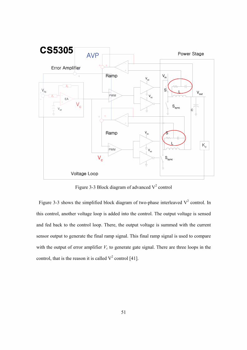
51
CS5305
Vref
Vfb
Z1
Z2
EA
Vc
Error Amplifier
Kd
PWM
S
Ssync
Vcc
Vcc
L
C
Vin
Vout
Power Stage
Voltage Loop
Ramp
S
Ssync
L
Vc
PWM Vcc
VccRamp
AVPCS5305
Vref
Vfb
Z1
Z2
EA
Vc
Error Amplifier
Kd
PWM
S
Ssync
Vcc
Vcc
L
C
Vin
Vout
Power Stage
Voltage Loop
Ramp
S
Ssync
L
Vc
PWM Vcc
VccRamp
AVP
Figure 3-3 Block diagram of advanced V2 control
Figure 3-3 shows the simplified block diagram of two-phase interleaved V2 control. In
this control, another voltage loop is added into the control. The output voltage is sensed
and fed back to the control loop. There, the output voltage is summed with the current
sensor output to generate the final ramp signal. This final ramp signal is used to compare
with the output of error amplifier Vc to generate gate signal. There are three loops in the
control, that is the reason it is called V2 control [41].

52
VoutVout
RampsRampsRamps
Current Ramp
Current Ramp
Current Ramp
Vc
Duty
Clock
VcVc
DutyDuty
ClockClock
Figure 3-4 Working wave for V2 control
Figure 3-4 shows the working waveforms. The output voltage ripple is added to current
sensor output to generate the final ramp signal. There, this final ramp is compared with
the control signal Vc. Since the output ripple is overlapped on the ramp signal, when the
output voltage changes due to the step of output load current, this change will directly
feedback to the control signal Vc and change the duty cycle. The inductor current will rise
or drop down quickly to support the new load current. This control can generate a very
fast transient response due to fast feedback of output voltage ripple. However, this
control has the same problem like LnLc control. A constant gain, which is proportional to
the output voltage error, is used for duty cycle compensation when output voltage
deviates from the reference value. This constant is always there even when the feedback
voltage is equal to the reference voltage. The switching ripple at the output voltage can
cause some duty cycle oscillation, which is going to generate a larger ripple at the output

53
voltage. In order to make the system stable, the feedback gain cannot be too large, which
means that the duty cycle will not saturate until the output voltage error is very large.
Besides linear-non-linear control and V2 control, there are a lot of other control
methods proposed in recent years to improve transient response of switching regulator.
According to [39], the ideal control should be like this: it must combine the best
advantages from the slow linear controls like the voltage mode control and the current
mode controls; and from the fast non-linear controls such as the hysteretic control and V2
control. These advantages are the following:
From the slow linear controls: Good load and line regulation in steady-state operation;
low output voltage ripple; and switching frequency independent of the filter parasitics.
From the fast non-linear controls: Optimized transient response under load current
steps; transient response independent of the load current steps amplitude; good stability in
transient-state operation; and easy to design and to implement.
A novel cotangent control is proposed in this work. This control combines the benefits
of both linear control like voltage control and current control and non-linear control
perfectly, which fits well these ideal control requirements from [39].

54
3.2.2. Proposed topology
driver
OP Z1(s)
Z2(s)
Vc
Vin Vout
RS
Q
LX
Compensator
PWM modulator
L
CR
RC
Vd
Vg
CS
COVref
driver
OP Z1(s)
Z2(s)
Vc
Vin Vout
RS
Q RS
Q
LX
Compensator
PWM modulator
L
CR
RC
Vd
Vg
CS
CS
COCOVref
Typical peak current control
Isense Ramp compensation
driver
OP Z1(s)
Z2(s)
Vc
Vin Vout
RS
Q
LX
Compensator
PWM modulator
L
CR
RC
Vd
Vg
CS
COVref
driver
OP Z1(s)
Z2(s)
Vc
Vin Vout
RS
Q RS
Q
LX
Compensator
PWM modulator
L
CR
RC
Vd
Vg
CS
CS
COCOVref
Typical peak current control
driver
OP Z1(s)
Z2(s)
Vc
Vin Vout
RS
Q
LX
Compensator
PWM modulator
L
CR
RC
Vd
Vg
CS
COVref
driver
OP Z1(s)
Z2(s)
Vc
Vin Vout
RS
Q RS
Q
LX
Compensator
PWM modulator
L
CR
RC
Vd
Vg
CS
CS
COCOVref
Typical peak current control
Isense Ramp compensation
Figure 3-5 Simplified block diagram of peak current control
From the analysis above, we can see that the most direct reason for the voltage drop or
spike at transient response is because the average inductor current is smaller or larger
than the load current during transient period. The end of the transient period is when the
average inductor current reaches the load current. Then the output voltage will stop
dropping or rising. So the final goal to speed up transient response is to make the average
inductor current reaches the new load current as fast as possible. In order to do that, let’s
take a look at a peak current controlled buck as shown in Figure 3-5. The average
inductor current is directly controlled by control signal Vc.

55
Vc
Ramp
compensation
Isense
Vg
Set pulse
ILoad
Vc
Ramp
compensation
Isense
Vg
Vc
Ramp
compensation
Isense
Vg
Set pulse
ILoadILoad
Vc’
Iload’
Vc’Vc’
Iload’Iload’
Figure 3-6 Modulation waveform at steady state for different loads
As shown in Figure 3-6 (Current Injection Control ⎯ CIC control), when the input and
output voltage are the same, the average duty-cycles are the same before and after the
load changes. If current sensor gain ks is constant (which is normally the case for most of
the controller), then the current sensor output will be proportional to load current. Let’s
take a look at the steady state modulation before and after the transient response as shown
in Figure 3-6. We will notice that the only difference is the level of control signal Vc
(assume Continuous Current Mode ⎯ CCM mode). If load current steps up, the control
signal Vc needs to go up to support more current. If the load current steps down, the error
signal needs to go down to reduce the average inductor current. The difference of the
control signal Vc before and after the load change is current sensor gain ks times the load
step LIΔ . In linear control, this process happens relatively slowly due to the limited
bandwidth and slew rate of error amplifier. So there is an unbalance between the average

56
inductor current and new load current, the output voltage will rise up or drop down. If we
can make this change happen quickly and force the control signal Vc to go into new
steady state in a short time, then the transient can be almost cancelled and output voltage
will not change too much. We call this a quasi-steady state now. This is some kind of
non-linear control. According to the ideal control requirements, we need the linear
control for the steady state to get a good line and load regulation. So we hope that the
non-linear control will not affect the steady state response of the main control loop. In
order to do this, a novel cotangent control is proposed.
A
Cotangent amp
Cotangent compensatorCotangent Cotangent
compensatorcompensator
ΔVcA
Cotangent amp
Cotangent compensatorCotangent Cotangent
compensatorcompensator
ΔVc
Fb
driver
OP Z1(s)
Z2(s)
Vc
Vin Vout
RS
Q
LX
Compensator
PWM modulator
L
CR
RC
Vd
Vg
CS
CO
Vref
driver
OP Z1(s)
Z2(s)
Vc
Vin Vout
RS
Q RS
Q
LX
Compensator
PWM modulator
L
CR
RC
Vd
Vg
CS
CS
COCO
Vref
Fb
driver
OP Z1(s)
Z2(s)
Vc
Vin Vout
RS
Q
LX
Compensator
PWM modulator
L
CR
RC
Vd
Vg
CS
CO
Vref
driver
OP Z1(s)
Z2(s)
Vc
Vin Vout
RS
Q RS
Q
LX
Compensator
PWM modulator
L
CR
RC
Vd
Vg
CS
CS
COCO
Vref
Figure 3-7 Block diagram for the cotangent control

57
Figure 3-7 is the simplified block diagram of the dead-banded non-linear control ⎯
cotangent control. A very fast (several ns) cotangent gain block is in parallel with the
original error amplifier. The output of the cotangent gain block is summed up with the
output of original error amplifier (or call compensator), then feed into the PWM
modulator. There, this compensated error signal Vc will compare with ramp signal and
generate a clock with certain duty cycle to turn on and turn off the power switches.
Dead band
Step up Step down
Dead band
Step up Step down
S1
S2
S3
S1
S2
S3
ARef
Fb ΔVc
cotangent ampcotangent ampRef Fb0.9Ref 1.1Ref
ΔVc
Ref Fb0.9Ref 1.1RefRef Fb0.9Ref 1.1Ref
ΔVc
Figure 3-8 I-V curve of the cotangent gain block
The I-V curve of cotangent gain block is shown in Figure 3-8. Since it looks like a
cotangent function, we call this control “cotangent control”. There is a dead band around
reference voltage. In the steady state, the output of the cotangent gain block is zero and
will not affect the linear control loop. The control loop is exactly classical current control
loop at steady state, which guarantees a good line, load regulation and steady state ripple.
During the step-up transient, when load rises up, the average inductor current is smaller
than load current. The output capacitor will supply most of the current and output voltage

58
will drop down. If the output voltage drops so much that Fb runs out of the dead band,
the output of the cotangent gain block cVΔ will not be zero and compensate control
signal Vc to a higher level. The higher voltage error happens at the output voltage, the
higher gain will generate at the cotangent block. Since the control voltage Vc rises up
much faster than original linear control, inductor current will rise up much faster to
support the new load current and keep the output voltage from dropping down even more.
By correctly choosing the gain of cotangent gain block and dead band dbΔ , we can make
the compensated error signal to a level so that it is enough but not over compensated to
support the changed load current. With the compensated error signal, the inductor current
will rise up quickly to the new load current level and output voltage will stop dropping
down. Since the output voltage is still below reference voltage at this time even if the
inductor current is equal to the load current, output of the linear error amplifier will rise
up due to the infinite DC gain of the error amplifier. Finally, the output of the linear error
amplifier will take over the control and support the load current. Cotangent gain block
will stop working when the output voltage is equal to reference voltage. The same
conditions will happen at the step-down transient. Since the cotangent gain block is much
faster than original error amplifier, this system is always stable if only the original control
loop is stable. Somehow, the non-linear gain block can even help the stability of the
whole system in the transient period to prevent the output voltage from running away.
3.2.3. Modeling of cotangent compensator
In order to model cotangent control, we redraw the block diagram of the cotangent
compensator in Figure 3-9. As we can see, there are two parts in this new compensator:
the first part is the original two-pole-one-zero compensator network used in the linear

59
control loop to compensate the linear peak current control. The delay of the block is in
“us” range. The output of this linear compensator will be used mostly at steady state to
get good linear regulation and output ripple. Another part is cotangent gain block. Since
this block is purely a gain block, the delay of this block is at “ns” range. The output of
this block will change immediately with the change in Fb signal. When load current steps
up or steps down, FB signal will change due to the change at output voltage. This change
will generate a compensation signal cVΔ at the output of cotangent gain block. This
compensation signal cVΔ will rise up or pull down the inductor current quickly in the
slew rate determined by inductor size and voltage difference across the main inductor.
When the inductor current reaches the new load current level, output voltage will stop
rising or falling. The “ns” cotangent gain block can speed up the transient response a lot.
Slow two-pole one-zero linear com,
“us” delay
Slow two-pole one-zero linear com,
“us” delay Fast cotangent amp, “ns” delay
Fast cotangent amp, “ns” delay
Cotangent Cotangent compensatorcompensator
OPZ1(s)
Z2(s)
Linear compensator
A
ΔVccompensator
Vref
FbVc
Cotangent Cotangent compensatorcompensator
OPZ1(s)
Z2(s)
Linear compensator
AA
ΔVccompensator
Vref
FbVc
Figure 3-9 Block diagram of cotangent compensator

60
If we consider the transfer function of the cotangent gain block, we will see that it is a
varying gain block. Assume the transfer characteristics of this cotangent gain block is the
following equations
when others0
dbrefxdbref Δ⋅+≤≤Δ⋅− 5.05.0)5.0( reff
fxctgA −−⋅ π when{=)(_ xctgComwhen others0
dbrefxdbref Δ⋅+≤≤Δ⋅− 5.05.0)5.0( reff
fxctgA −−⋅ π when{=)(_ xctgCom
, we can see that there are three parameters in this transfer function: magnitude A,
frequency f and dead band dbΔ .
0 0.1 0.2 0.3 0.4 0.5 0.6 0.7 0.8 0.9 1100
75
50
25
0
25
50
75
100
Cont_gain x 1, 1,( )
Cont_gain x 10, 1,( )
Cont_gain x 20, 1,( )
xa
A=1
A=10
A=20
Figure 3-10 Cotangent function with different magnitude A

61
Figure 3-10 shows the characteristics of cotangent function with different magnitude
A. From the figure, we can see that, the larger A, the larger gain with same voltage error.
When A is close to zero, the cotangent function is more like a segmented Y-axis and the
system is like a bang-bang control. When A is increasing, the curve is approaching Y-
axis. A larger compensation signal VcΔ can be injected into the control signal with the
same voltage error at the feedback signal Fb. When A is very large, the system is going to
be unstable. So the selection of magnitude A is a trade off between fast transient response
and stability.
0 0.1 0.2 0.3 0.4 0.5 0.6 0.7 0.8 0.9 1100
75
50
25
0
25
50
75
100
Cont_gain x 1, 1,( )
Cont_gain x 1, 1.5,( )
Cont_gain x 1, 2,( )
x
a
0 0.1 0.2 0.3 0.4 0.5 0.6 0.7 0.8 0.9 1100
75
50
25
0
25
50
75
100
Cont_gain x 1, 1,( )
Cont_gain x 1, 1.5,( )
Cont_gain x 1, 2,( )
x
a
f=1
f=1.5
f=2
Figure 3-11 Cotangent function with different frequency f

62
Figure 3-11 shows the cotangent function with different frequencies. With different
frequency, the saturation level at which the gain of cotangent function is infinite is
different. The higher frequency, the smaller saturation level and the duty cycle can be
saturated earlier. With a higher frequency for this cotangent function, the transient
response is going to be faster. However, when the frequency is too high, the system is
going to oscillate and cause the stability problem.
The selection of dead band dbΔ will depend on the steady state ripple at the output
voltage. If the dead band is too small, there is some gain from the cotangent block even at
steady state. This gain is going to cause some noise at the duty cycle and generate larger
output voltage ripple. However, if the dead band is too large, the cotangent control is not
going to kick in until the output voltage error is really large, which is not normally what
we want.
Now, let’s go back to the diagram shown in Figure 3-9, we will see that the output of the
whole compensator is actually the sum of the output of original two-pole-one-zero
compensation network and the output of cotangent gain block. Comparing with the linear
control, cotangent control essentially adds a varying DC gain in parallel with the original
linear error amplifier. If we add a DC gain to the transfer function of the original error
amplifier, we will see that, the cotangent gain block adds a zero to the whole transfer
function from Fb to Vo. Figure 3-12 shows the transfer function of the whole cotangent
compensator. A is the gain of cotangent gain block. With the gain increase, the zero will
move to low frequency and increase the bandwidth of the whole compensator. At steady
state, the whole compensator will damp the high frequency noise from the output voltage.
It seems like a door, only during the transient, the door is going to open and pass through

63
the high frequency signal from the output to speed up transient response. At steady state,
the door is closed for high frequency part and only passes through the low frequency
signal. At both the beginning and the end of the transient, the transfer function of the
whole compensator is the original compensator. That is the major difference between this
control and the other nonlinear controls.
A=0.05A=0
A=0.5
A=5
A=50
Gain(dB)
Phase(o)
(Hz)
A=0.05A=0
A=0.5
A=5
A=50
Gain(dB)
Phase(o)
(Hz)
Transient beginTransient begin
Transient recoverTransient recover
Figure 3-12 Transfer function of the cotangent compensator

64
Put this transfer function into Dr. Ridley’s model, we can get the whole system loop
gain shown in Figure 3-13. From the system loop gain T2, we can see that, with cotangent
control, when transient begins, the output voltage will drop down or rise up, the more
output voltage error happens, the higher loop gain will be generated from this control
loop. The cotangent control will speed up the recover process significantly. When the
output voltage recovers to the reference value, the gain of the cotangent gain block will
disappear and the whole system loop gain of the cotangent control is exactly the original
linear peak current control loop gain. It means that cotangent control will only work
during the transient period to speed up the transient recover process and reduce the output
voltage error. It will not affect any steady state performance of the original linear control.
That is the big benefit of this control comparing with LnLc control and V2 control.
From the analysis above, we can see that, the control loop gain is changing during
transient period, which means that the system is a timing varying system. The classical
control theory such as phase margin, gain margin and bandwidth concept cannot be used
in this system to determine the stability. How to model and design the stability of this
system is a challenge. However, as we discussed above, when the magnitude of cotangent
control A is too large or the frequency f is too high, the system is going to be unstable. So
there is an optimized value for these design variables. How to model the stability of this
time-varying system and design these design variables are a big challenge. Next section
will focus on the stability modeling of this system.

65
Transient recover
Transient begin
Gain(dB)
Phase(o)
(Hz)
Transient recover
Transient begin
Transient recover
Transient begin
Gain(dB)
Phase(o)
(Hz)
Transient recover
Transient begin
Gain(dB)
Phase(o)
(Hz)
Transient recover
Transient begin
Transient recover
Transient begin
Gain(dB)
Phase(o)
(Hz)
Figure 3-13 System loop gain for the cotangent control
3.2.4. Stability modeling of the time-varying system ⎯ cotangent
control
Control system analysis is based on the concept that the system is linear. However,
that's not always true, but the reason that designers do that is that there are very few
analytical techniques that can be used to predict the behavior of nonlinear systems
[42]. Prediction is the key here. When control systems are designed it is imperative that
users and customers know how the system will behave in all situations. Linear analysis
techniques are good in that way because you can guarantee stability, for example. You

66
would know that the system is stable and that the stability of the system was in no way
dependent upon the conditions in the system, either the input(s) or the initial state of the
system [43].
Nonlinear systems present a problem in that regard. Here are some facts about
nonlinear systems.
Nonlinear systems can exhibit instability when certain inputs are applied but may
be well behaved (stable) for all other inputs.
Nonlinear systems often have limit cycles, in which sustained oscillations occur
but only at a particular amplitude and frequency. Linear systems might oscillate at
a particular frequency, but oscillation at particular amplitude is a phenomenon
peculiar to nonlinear systems.
There are very few analytical techniques that can be used to predict behavior of
nonlinear systems. General techniques for analysis of nonlinear systems are hard
or impossible to find and we are often left to use very specific techniques for
special situations and we are not able to make general statements. To make
predictions of nonlinear system behavior, designers often use
simulations. However, doing a simulation of a nonlinear system only tells the
designer about that situation. There could be other situations in which the system
misbehaves, and the designer will only find that out if s/he does a simulation for
that specific situation.
As we discussed above, switching regulator is a non-linear system. However, it is a
very special system. Most of the switching regulator can be roughly simplified into the
system diagram shown in Figure 3-14. For cotangent control, the non-linear function is

67
the transfer function of the contingent compensator. G(s) is the transfer function of the
other part including the power stage, current loop, PWM modulator etc. This system has
the following characteristics:
The system is autonomous, i.e. it has no input.
The system oscillates. At any point in the system there will be a periodic signal.
G(s) is a system that is a low-pass filter.
Since a low pass filter G(s) is present in this system, the high order harmonics generated
by the non-linear block are filtered out. Only the fundamental frequency components left
in the final output. For this kind of system, an approximation method called “describing
function” method can be used to model the stability problem.
Non-linear part DF
Non-linear part DF
linear partLow pass filter
G(s)
linear partLow pass filter
G(s)
input Output
Figure 3-14 Typical system diagram for a switching regulator
A describing function is roughly the ratio of the magnitude of the output of non-linear
block and the magnitude of the input signal. It is going to be a function of variable of
magnitude A, frequency f, and dead band for cotangent control [43][44][45].

68
Assume the nonlinearity is denoted by f(x,t). The input x(t) is assumed to be
),sin()( tEtx ω=which results in the output
).),sin(()( ttEfty ω=
The describing function gain,K(E,ω), is the fundamental of the Fourier series representation of this periodic output, y(t), divided by the input amplitude E. Thus, the describing function gain is given by
∫ +=T
dttjtttEfTE
EK0
.)}cos()){sin(),sin((2),( ωωωω
The final expression of the describing function for cotangent control is really
complicated. If we use a segmented linear function as shown in Figure 3-15 to
approximate the cotangent function and assume that only the cotangent gain block is
working during the transient period, we can get the describing function of this cotangent
compensator.
Non-linear part DF
linear partLow pass filter
G(s)
linear partLow pass filter
G(s)
input Output
Figure 3-15 Approximation system block diagram for cotangent control

69
Figure 3-16 Relationship of output of segmented linear function with input signal amplitude A
Figure 3-16 is a plot of the output of the saturating amplifier against the input
amplitude, A[46][47]. Under this assumption, the describing function of the non-linear
compensator is equation (3-5)
21 )/(1)/()/([sin2)( AAAAAAADF satsatsat −+= −
π (3-3)
Figure 3-17 shows the plot of the describing function plotted against A, the input
amplitude to the nonlinearity.

70
Figure 3-17 Plot of the describing function plotted against A, the input amplitude to the nonlinearity
According to the system block diagram shown in Figure 3-15, the system will be unstable
when
DF(A)G(jw) = -1 ( 3-4 )
Plot both DF(A) and G(jw) on Nyquist plot, we can get Figure 3-18. If there is an
intersection, then there will be oscillations in the system. The frequency at which the
frequency responses intersect determines the frequency of the oscillations. The amplitude
at which the negative inverse describing function intersects determines the amplitude of
the oscillations [48][49]. By using this method, we can get the optimized value for the
parameters for the non-linear blocks.

71
Figure 3-18 Nyquist plot of DF(A) and G(jw)
3.2.5. Comparison between cotangent control and other control
methods
In this section, we will do a comparison between cotangent control and other control
methods. Figure 3-8 shows the I-V curve of cotangent gain block. In this plane, X-axis is
the feedback voltage and Y-axis is the additional compensated control signal cVΔ
generated by non-linear block in parallel with the original error amplifier. Our
comparison will be done in this plane.
In original linear peak current control, there is no other gain block in parallel with
original error amplifier, so the equivalent I-V curve for linear peak current control in this
plane is X-axis of the plane as shown in Figure 3-19.

72
Dead band
Step up Step down
Dead band
Step up Step down
S1
S2
S3
S1
S2
S3
Ref Fb0.9Ref 1.1Ref
ΔVc
Ref Fb0.9Ref 1.1RefRef Fb0.9Ref 1.1Ref
ΔVc
Linear controlLinear control
Figure 3-19 Comparison between linear control and cotangent control
Dead band
Step up Step down
Dead band
Step up Step down
S1
S2
S3
S1
S2
S3
LnLcLnLc
Ref Fb0.9Ref 1.1Ref
ΔVc
Ref Fb0.9Ref 1.1RefRef Fb0.9Ref 1.1Ref
ΔVc
Figure 3-20 Comparison between Cotangent control and LnLc control
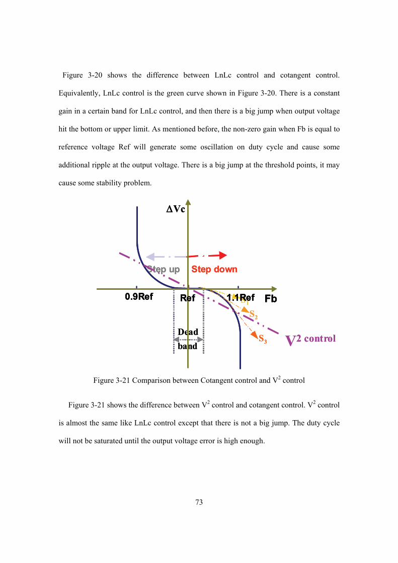
73
Figure 3-20 shows the difference between LnLc control and cotangent control.
Equivalently, LnLc control is the green curve shown in Figure 3-20. There is a constant
gain in a certain band for LnLc control, and then there is a big jump when output voltage
hit the bottom or upper limit. As mentioned before, the non-zero gain when Fb is equal to
reference voltage Ref will generate some oscillation on duty cycle and cause some
additional ripple at the output voltage. There is a big jump at the threshold points, it may
cause some stability problem.
Dead band
Step up Step down
Dead band
Step up Step down
S1
S2
S3
S1
S2
S3 V2 controlV2 control
Ref Fb0.9Ref 1.1Ref
ΔVc
Ref Fb0.9Ref 1.1RefRef Fb0.9Ref 1.1Ref
ΔVc
Figure 3-21 Comparison between Cotangent control and V2 control
Figure 3-21 shows the difference between V2 control and cotangent control. V2 control
is almost the same like LnLc control except that there is not a big jump. The duty cycle
will not be saturated until the output voltage error is high enough.

74
Dead band
Step up Step down
Dead band
Step up Step down
S1
S2
S3
S1
S2
S3
Traditional non-linear control
Traditional non-linear control
Ref Fb0.9Ref 1.1Ref
ΔVc
Ref Fb0.9Ref 1.1RefRef Fb0.9Ref 1.1Ref
ΔVc
Figure 3-22 Comparison between Cotangent control and traditional bang-bang control
Figure 3-22 shows the difference between the traditional non-linear control ⎯ bang-
bang control and cotangent control. Equivalently, bang-bang control is a segmented Y-
axis in this plane. As mentioned before, linear peak current control looks like an X-axis.
We can see that cotangent control makes a very smooth transition from linear control to
an infinite gain bang-bang control. Cotangent control keeps the high steady-state
performance of linear peak current control, meanwhile generates a fast transient response
of bang-bang control without causing the stability problem. Cotangent control exactly fits
the ideal control concept proposed in [39]!

75
3.2.6. Combination of cotangent control with new non-linear active
clamp
A
Cotangent amp
Cotangent compensatorCotangent Cotangent
compensatorcompensator
ΔVcA
Cotangent amp
Cotangent compensatorCotangent Cotangent
compensatorcompensator
ΔVc
Fb
driver
OP Z1(s)
Z2(s)
Vc
Vin Vout
RS
Q
LX
Compensator
PWM modulator
L
CR
RC
Vd
Vg
CS
CO
Vref
driver
OP Z1(s)
Z2(s)
Vc
Vin Vout
RS
Q RS
Q
LX
Compensator
PWM modulator
L
CR
RC
Vd
Vg
CS
CS
COCO
VrefA
Cotangent amp
Cotangent compensatorCotangent Cotangent
compensatorcompensator
ΔVcA
Cotangent amp
Cotangent compensatorCotangent Cotangent
compensatorcompensator
ΔVc
Fb
driver
OP Z1(s)
Z2(s)
Vc
Vin Vout
RS
Q
LX
Compensator
PWM modulator
L
CR
RC
Vd
Vg
CS
CO
Vref
driver
OP Z1(s)
Z2(s)
Vc
Vin Vout
RS
Q RS
Q
LX
Compensator
PWM modulator
L
CR
RC
Vd
Vg
CS
CS
COCO
Vref
Fb
driver
OP Z1(s)
Z2(s)
Vc
Vin Vout
RS
Q
LX
Compensator
PWM modulator
L
CR
RC
Vd
Vg
CS
CO
Vref
driver
OP Z1(s)
Z2(s)
Vc
Vin Vout
RS
Q RS
Q
LX
Compensator
PWM modulator
L
CR
RC
Vd
Vg
CS
CS
COCO
Vref
AsGm
AsGm
Vref
VFB
Iout
Active ClampActive Clamp
V-
V+
V+
V-
AsGm
AsGm
Vref
VFB
Iout
Active ClampActive Clamp
V-
V+
V+
V-
Figure 3-23 Combination of cotangent control and fast non-linear active clamp control
As mentioned before, the inductor current cannot change dramatically when the load
current steps up or steps down. This delay of the inductor current rising or falling will
cause some voltage error at the output capacitor. For a high input voltage, low output
voltage case, this problem is going to cause a large voltage spike at the output. During
step-down transient, there is a big current that is equal to the load current at the beginning
of the transient period. When the load current drops down to zero suddenly, inductor
current is going to keep for a while. All of the inductor current will be dumped into the
output capacitor and cause a big voltage spike at output voltage. If the bandwidth of

76
control loop is infinite, the control loop will shut down both high side device and low
side device, the inductor current will keep dropping to zero. All of the additional energy
25.0 IL ⋅⋅ in inductor will still be dumped into the output cap and cause voltage spike at
output voltage. Traditional switching regulator can do nothing for this additional energy
but use a bigger output cap. But this is going to increase cost and area. Comparing with
traditional linear controlled switching regulator, active clamp is a good option for fast
transient response application. With proper design, active clamp can generate a very high
bandwidth because there is no compensator in the control loop. Figure 3-23 is the
combination of a general structure active clamp and cotangent control [50]. The left part
in Figure 3-23 is a single-phase cotangent control buck regulator. A resonant tank
consisting with an inductor and capacitor is included in the output stage. The right part is
an active clamp structure. There are two paths (pull-up path and pull-down path)
connected directly to the output node. When the feedback voltage VFB is lower than the
low-band reference, a pull up current will be generated and fed into the output node Vout
to rise up output voltage Vout. If the feedback voltage VFB is larger than the high-band
reference, a pull down current will be generated and pull down the output voltage Vout.
Since active clamp bypasses inductor and is connected directly to the output cap, it can
quickly source and sink current during the step-down transient and prevent the
overshooting of the output voltage. This is the biggest advantage for active clamp
comparing with traditional linear control. However, active clamp has a poor efficiency
when the voltage difference between input and output voltage is large. If it is used most
of the time, it is going to affect the efficiency a lot. Active clamp can’ t replace the
traditional switching regulator totally to supply the power to the system. Combining the

77
efficient fast transient cotangent control switching regulator and fast transient active
clamp, we can get a combinational system with a good efficiency at steady state by
traditional switching regulator and fast transient response by cotangent control and active
clamp at transient period.
3.2.7. Verification
In order to verify the cotangent control, a high frequency synchronous buck DC-DC
converter IC with cotangent control is designed. Figure 3-24 is the comparison of output
voltage during transient of linear control and cotangent control. The first picture is the
comparison of the output voltage. From the picture, we can see that the improvement is
obvious. With cotangent control, the output voltage stops dropping immediately since the
inductor current rises up to the load level immediately as shown in the second picture.
However, from the third picture, which is the output of original error amplifier and the
output of cotangent gain block cVΔ , we can see that the output of the original error
amplifier will rise up slowly. The output of cotangent gain block is high at the beginning
of the transient, then reduce to zero when the transient period ends. The same phenomena
happen at the step-down transient. Cotangent control reduces the voltage error a lot at
both step-up and step-down transient. However, cotangent control does increase the
settling down time a little bit.

78
Figure 3-24 Transient response (5V->1.5V, 0.2A load, 1A step)
Figure 3-25 shows another extreme case. In this case, the load current is zero and
output voltage is higher than the reference at the beginning. When the load current steps
up from zero current to full load current, the output voltage will have a very large voltage
drop. However, there is no large voltage drop for cotangent control. The improvement for
the transient response is significant. The reason for the big voltage drop at step-up
transient for linear control is that, the error amplifier is deeply saturated at the beginning

79
of the transient period. It will take a long time for the output of error amplifier to go back
to the steady state value. The slew rate of the error signal is strongly limited due to the
large time-constant passive network in the compensation network. For cotangent control,
this problem is bypassed due to the fast response of cotangent gain block. The error
signal can rise up quickly to the new level and support the new load current.
Figure 3-25 Transient response from DCM to CCM

80
3.2.8. Summary
Fast transient response is an important requirement for most of the switching DC-DC
converters, especially for portable application since the output voltage is going lower and
lower and the tolerance is smaller and smaller. For a traditional linear peak current
control, the rising speed of inductor current during the step up transient period is strongly
limited by the bandwidth of the control loop and slew rate of the error amplifier. At
another extreme case, if a bang-bang control is used to saturate the duty cycle during
transient period, a stability problem can happen for some case and the inductor current
may oscillate. A novel control scheme ⎯ Cotangent control is proposed to speed up the
transient response. Comparing with linear control and existing non-linear control, this
control has better performance at both steady state and transient period.

81
3.3. Active feedback compensator and adaptive compensation
Compensator is a critical part in the whole converter system. It will affect the stability
and the transient response of the whole system. How to design a good compensator to
stabilize the whole system in a whole working range is always a challenge for power
management IC design. For monolithic switching DC-DC converter, this issue is more
serious due to the limited silicon area. As we know, most of the switching regulator need
some low frequency zeros and poles in the compensator. To generate a low frequency
zero and pole, some large value passive components are needed. It will take a lot of
silicon area to build large size passive components on silicon. For monolithic integration
of switching regulator, this is a big challenge. In order to solve this issue, a novel active
feedback compensator is proposed to reduce the silicon area for on-chip compensator in
this section. A commonly used two-pole-one-zero compensator network used for peak
current control is used as example through the discussion. The design concepts proposed
in this section can be used for any general switching regulator. After the active feedback
compensator, an adaptive compensation concept is proposed for both buck and boost
converter to stabilize the whole system for a wide working range.
3.3.1. Active feedback compensator
Compensator can be implemented using different kinds of real circuitry. Figure 3-26 is a
widely used op-amp based one-zero-two-pole compensator network for peak current
controlled switching DC-DC converter. The op amp used in this network is an ideal op
amp. The transfer function of this compensator network is shown as following equations:

82
)1(
1)( 0
p
zvv ss
s
HsH
ω
ω
+⋅
+⋅= (3-5)
The DC gain of this network is
220
1CRRR
RH
yx
yv ⋅
⋅+
= (3-6)
The zero of this network is
( ) 121
1CRRz ⋅+
=ω (3-7)
and the pole of this network is
11
1CRp ⋅
=ω (3-8)
Figure 3-26 Op-amp based one-zero-two-pole compensator network for peak current
control switching DC-DC converter

83
According to equation (3-5), if we assume 400000 =vH , R2=500k, kz ⋅⋅⋅= 12 πω ,
410083.32 ⋅⋅⋅= πω p , we have Rx=17.5k, Ry=10k, R1=16.7K, R2=500k, C1=308pF,
C2=18.2pF. C1 is too big for on-chip implementation. This big capacitor is caused by the
low frequency zero needed to compensate the low frequency pole at the control to output
transfer function with current loop closed. It is a critical component in this compensator
network. However, it is almost impossible to build this kind of big cap on silicon, which
means that we cannot directly implement this compensator network on silicon. How to
generate a low frequency zero and pole for on-chip implementation of the compensator?
In order to get a low frequency zero or pole, a large capacitor or resistor is needed. As
we know, it is difficult to implement a large value capacitor or a resistor on silicon. A
capacitance or resistance booster is needed to generate a large equivalent resistor or
capacitor. Figure 3-27 shows a miller effect capacitance booster. From the transfer
function of this block, we can see that the equivalent capacitance is boosted up by β
times. By using a small resistor and capacitor, a large time constant RC can be generated
by miller effect. Using this miller effect capacitance booster, we can generate a low
frequency pole using a small silicon area! Besides the low frequency pole, a low
frequency zero may be needed in the compensator like peak current control switching
DC-DC converter. How to get this kind of low frequency zero?

84
R2
C2
βXVz
Vc’
R2
C2
βXVz
Vc’
22)1(1 CRsVV
c
z
⋅⋅++−=
∂∂
ββ
Figure 3-27 Miller effect capacitance booster
In order to answer this question, let’s take a look at another basic block shown in
Figure 3-28. From the transfer function of a negative feedback loop, we can see that, if
only the loop gain βα ⋅ >>1, the whole transfer function gain is the inverse of the
feedback gain. If the feedback gain α is a miller effect capacitance booster shown in
Figure 3-27, we can implement a low frequency zero using a small silicon area! By
combining the low frequency zero, low frequency pole and simple voltage gain, we can
get any kind of the compensation transfer function using a small silicon area, which
makes it possible to monolithically integration of any switching frequency DC-DC
converter.

85
αβαβ βα 1
1
1>>⋅
≈⋅+
=∂∂
c
o
VV
β
VoVc
α
β
VoVc
α
Figure 3-28 Negative feedback loop inverse a transfer function
Since peak current control is widely used in reality, now we will focus on the
implementation of a general structure for the compensator used for peak current control.
As shown in equation (3-11), a general two-pole-one-zero transfer function can be
transformed into a pure DC gain times an integrator and a close loop gain with an active
feedback. Since the active feedback block plays an important role in the whole
compensator, we call the whole compensator “active feedback compensator”.
ss
Hss
sH
ss
s
HsH
z
zpzp
v
p
z
z
pv
p
zvv
+
−+
⋅⋅⋅
=++
⋅⋅⋅
=+⋅
+⋅=
ωωωωωω
ωω
ω
ω
ω
1
111
)1(
1)( 00
0 (3-9)
According to equation (3-11), a general compensator structure is proposed as shown in
Figure 3-29. The first stage of this structure is two source followers for level shift and is
used to generate high input impedance. The second stage of this structure is an integrator
used to generate a pole at zero frequency as shown in equation (3-11). The third stage is
an active feedback for a zero and a pole in equation (3-11).

86
Vc
1
1
OPα
γ
R1
C1
R2
C2
Vref
Vfb
Vi
Vzβ
Vzf
φVc
’
Source follower for level shift and high input impedance
Active feedback for zero and pole
For large range of Vc
Integrator
Vc
1
1
OPα
γ
R1
C1
R2
C2
Vref
Vfb
Vi
Vzβ
Vzf
φVc
’
Source follower for level shift and high input impedance
Active feedback for zero and pole
For large range of Vc
Vc
1
1
OPα
γ
R1
C1
R2
C2
Vref
Vfb
Vi
Vzβ
Vzf
φVc
’
Vc
11
11
OPαα
γγ
R1
C1
R2
C2
Vref
Vfb
Vi
Vzβ
Vzf
φφVc
’
Source follower for level shift and high input impedance
Active feedback for zero and pole
For large range of Vc
Integrator
Figure 3-29 A general compensator structure for peak current control
The transfer function of this structure is derived as following.
The transfer function of the second stage is
11
1CRsV
V
fb
i
⋅⋅−=
∂∂
(3-10)
The feedback gain of the third stage is
22' )1(1 CRsV
Vc
zf
⋅⋅++⋅
=∂
∂
ββγ
(3-11)
The feed forward gain of the third stage is
22)1(1' CRsVV
c
z
⋅⋅++−=
∂∂
ββ (3-12)

87
The transfer function of the whole structure is
22
22
11
)1(11
)1(11
1)1(
CR
sCR
s
sCRVV
fb
c
⋅⋅+⋅+
+
⋅⋅+
+
⋅⋅⋅+⋅⋅
⋅−=
∂∂
ββγ
ββγ
φα (3-13)
From equation (3-11), we can see that, the DC gain of this general block is
)1(110 βγ
φα⋅+⋅⋅
⋅−=
CRHv (3-14)
the low frequency zero is
22)1(1
CRz ⋅⋅+=
βω (3-15)
and high frequency pole is
22)1(1
CRp ⋅⋅+⋅+
=β
βγω (3-16)
By using a large β , we can use a small resistor R2 and capacitor C2 to generate a low
frequency zero. After the selection of R2 and C2, we can select γ for the required high
frequency pole. Then we can choose R1, C1, α and φ for the correct DC gain. The
following is a general design procedure for this compensator
• Choose R2, C2 and β for the required zero
• Choose γ for the second pole
• Choose R1, C1,α and φ for the correct DC gain

88
3.3.2. Active compensation for buck
Gv
Gdi
Gdv
Fm
-Hi
He
-Hv
Vin Vout
dTv
Ti
Vc
iL
Gv
Gdi
Gdv
Fm
-Hi
He
-Hv
Vin Vout
dTv
Ti
Vc
iL
Figure 3-30 Simplified system block diagram for peak current control
One chip for multi markets is a normal case in industry now. The input voltage, output
voltage, load current and even switching frequency for the same chip in different
applications may be quite different. Since compensator, ramp compensation and current
sensor are integrated inside the chip for monolithically integrated chip, the end user
cannot change the compensation to fit a specific application. Besides this, the poles and
zeros in the control loop may change with the application conditions and even
temperature; it is almost impossible to stabilize the system with a fixed compensator on
chip for all of the application cases using traditional compensator structure. How to
design a fixed compensator to stabilize the system for wide input and output ranges is a
big challenge.

89
Gvd Control-to-output transfer function
-1.00E+02
-8.00E+01
-6.00E+01
-4.00E+01
-2.00E+01
0.00E+00
2.00E+01
1.00E+00 1.00E+01 1.00E+02 1.00E+03 1.00E+04 1.00E+05 1.00E+06 1.00E+07
frequency (Hz)
gain
(dB
)
Figure 3-31 Control to output transfer function with current loop closed
Figure 3-30 shows the simplified system block diagram for a typical peak current
control. The system can be simplified to a simple two-loop control system with current
loop as the inner loop. As shown in Figure 3-31, according to [22], when the current loop
is closed, the power stage is degraded to a one-order system. The compensation is
designed based on the transfer function Goc from Vc to Vout. For different applications, the
dominant pole ωpdom of Goc are moving with duty cycle D and load current as shown in
equation (3-19).
)5.0'(1−⋅⋅
⋅+
⋅≅ Dm
CLT
CR cs
pdomω (3-17)

90
R is the load resistance, C is the output capacitor, L is the main inductor, Ts is switching
period, mc is the ratio of inductor current slope and ramp compensation slope, D’ is 1-D
(D is duty cycle)
In order to make the system loop stable for different applications, adaptive
compensation concept is proposed, which means that the zero in the compensator will
move to low frequency when load current increases. Design is made based on the worst-
case operation situation. All of the working conditions are then evaluated to guarantee the
stability for all operation ranges. A non-linear saw tooth signal shown in Figure 3-5 is
used for slope compensation when duty cycle is larger than 50%. Although it is quite
difficult to make the single pole of control-to-output transfer function with current loop
closed to be equal to the compensation zero when input, output voltage, load current and
even switching frequency change, the test results show that the designed chip works well
over a wide operation ranges.

91
3.3.3. Adaptive compensation for boost
L LX
OP Z1(s)
Z2(s)
Vc
Vin Vout
RS
Q
Compensator
CR
RC
Vd
CO
REF
ramp&
clock
CS
CO Current limit
Driver&
dead time
L LX
OP Z1(s)
Z2(s)
Vc
Vin Vout
RS
Q RS
Q
Compensator
CR
RC
Vd
CO
REF
ramp&
clock
CS
COCO Current limit
Driver&
dead time
Figure 3-32 Simplified block diagram for peak current control boost converter
In this section, we will expand the adaptive compensation concept to boost converter.
It is more difficult to compensate a boost converter due to the right half plane zero.
Figure 3-32 shows the simplified diagram for peak-current PWM control for boost
converter. Since the right half-plane zero and resonant poles of the power stage for boost
move according to duty cycle D (D’=1-D) and load current, it is quite difficult to design
a fixed on-chip compensator to stabilize the converter system for a wide operation range.
For monolithic integration, since the compensator, ramp compensation and current sensor

92
are fixed inside the silicon; the loop-gain design for the monolithic boost converter
becomes very challenging.
According to Ridley [22], when the current loop is closed, the power stage is degraded
to a one-order system. The compensation is designed based on the transfer function Goc
from Vc to Vout. Figure 3-33 shows the bode plot of Goc. There are a dominant pole ωpdom,
a right half-plane zero ωRHZ and a double-pole at the half switching frequency in Goc. For
different applications, the dominant pole ωpdom and right half-plane zero ωRHZ move with
duty cycle D and the load current, as shown in Figure 3-33. In order to make the system
stable for all cases, it is good to keep ωpdom and ωRHZ constant for different applications
(different Vin, Vout and load current) so that a fixed compensator can be used to
compensate the whole system.
For this purpose, we proposed the following two constant-ripple design approaches.
Constant inductor current ripple assumption:
α⋅−⋅=⋅
⋅−⋅=−⋅⋅=Δ s
ins
out
insins
out
ininsL T
LVT
LVVT
LVT
VV
LVTI
2
)1( (3-18)
Constant output voltage ripple assumption:
sloadout
insloadout TI
CVVTIV ⋅⋅=
⋅⋅⋅
=Δ β (3-19)
In this design approach, α and β should be selected as constants. Based on (3-20) and
(3-21), the ωpdom and ωRHZ can be simplified as

93
in
load
out
loadpdom V
ICV
ICR
βω ⋅⋅=
⋅⋅
=⋅
≅222
(3-20)
loadloadout
inRHZ ILIV
VL
RD αω =⋅⋅
=⋅
=22'
(3-21)
-270-240-210-180-150-120-90-60-30
0
1.00E+00 1.00E+01 1.00E+02 1.00E+03 1.00E+04 1.00E+05 1.00E+06
freq (Hz)
phas
e(de
g)
Goc Vin=1.2 Vout=3.3 Iload=0.5A Goc Vin=1.2 Vout=3.3 Iload=0.1AGoc Vin=2.4 Vout=3.3 Iload=0.5A Goc Vin=2.4 Vout=3.3 Iload=0.1A
-40
-30
-20
-10
0
10
20
1.00E+00 1.00E+01 1.00E+02 1.00E+03 1.00E+04 1.00E+05 1.00E+06
freq (Hz)
gain
(dB
)
Pdom move with D’, Iload
ZRHZ move with D’, Iload
Double-pole at 0.5fs
-270-240-210-180-150-120-90-60-30
0
1.00E+00 1.00E+01 1.00E+02 1.00E+03 1.00E+04 1.00E+05 1.00E+06
freq (Hz)
phas
e(de
g)
Goc Vin=1.2 Vout=3.3 Iload=0.5A Goc Vin=1.2 Vout=3.3 Iload=0.1AGoc Vin=2.4 Vout=3.3 Iload=0.5A Goc Vin=2.4 Vout=3.3 Iload=0.1A
-40
-30
-20
-10
0
10
20
1.00E+00 1.00E+01 1.00E+02 1.00E+03 1.00E+04 1.00E+05 1.00E+06
freq (Hz)
gain
(dB
)
Pdom move with D’, Iload
ZRHZ move with D’, Iload
Double-pole at 0.5fs
Figure 3-33 Transfer function Goc changes for different application cases

94
Now, ωpdom is close to a constant and ωRHZ will only change with load current. Figure
3-34 shows Goc under the assumptions. Compared with the Goc in Figure 3-34, the Goc in
Figure 3-34 allows for much easier compensation by a two-pole-one-zero network.
-270-240-210-180-150-120-90-60-30
0
1.00E+00 1.00E+01 1.00E+02 1.00E+03 1.00E+04 1.00E+05 1.00E+06
freq (Hz)
phas
e(de
g)
Goc Vin=1.2 Vout=3.3 Iload=0.5A Goc Vin=1.2 Vout=3.3 Iload=0.1A
Goc Vin=2.4 Vout=3.3 Iload=0.5A Goc Vin=2.4 Vout=3.3 Iload=0.1A
-40
-30
-20
-10
0
10
20
1.00E+00 1.00E+01 1.00E+02 1.00E+03 1.00E+04 1.00E+05 1.00E+06
freq (Hz)
gain
(dB
)
Pdom close to constant
ZRHZ only change with Iload
Figure 3-34 Transfer function Goc with constant ripple assumption

95
Figure 3-34 shows that when the load current increases, the DC gain of Goc will drop
down and ωRHZ will move to a lower frequency. If the second pole of the compensator is
much higher than ωRHZ due to the rise of load current, the final system loop gain may rise
above unity gain and cause the system to be unstable. In order to achieve high bandwidth
and stability for different series of duty cycle D and different load current; Adaptive
compensation concept is used. In the adaptive compensation, when the load current
increases, the DC gain of the compensator will increase; meanwhile, the second pole will
move to lower frequency to damp the ωRHZ of Goc so that the gain of Goc will not rise
above 0 dB and cause stability problems. Figure 3-35 shows the adaptive compensation
concept, and Figure 3-36 shows the system loop gain at different conditions. The
bandwidth of the system loop gain is close to a constant 10 kHz for different application
conditions. The stability is obviously improved by constant ripple assumptions and
adaptive compensation.

96
-200
-170
-140
-110
-80
-50
-20
10
1.00E+00 1.00E+01 1.00E+02 1.00E+03 1.00E+04 1.00E+05 1.00E+06
freq (Hz)
phas
e(de
g)
Goc Vin=1.2 Vout=3.3 Iload=0.5AGoc Vin=1.2 Vout=3.3 Iload=0.1AGoc Vin=2.4 Vout=3.3 Iload=0.5Acompensator for Vin=1.2 Vout=3.3 Iload=0.5A Conpensator for Vin=2.4 Vout=3.3 Iload=0.5AConpensator for Vin=1.2 Vout=3.3 Iload=0.1A
-40
-20
0
20
40
60
80
1.00E+00 1.00E+01 1.00E+02 1.00E+03 1.00E+04 1.00E+05 1.00E+06
freq (Hz)
gain
(dB
)
Figure 3-35 Adaptive compensation concept

97
-270-240-210-180-150-120-90-60-30
0
1.00E+00 1.00E+01 1.00E+02 1.00E+03 1.00E+04 1.00E+05 1.00E+06
freq (Hz)
phas
e(de
g)
Goc Vin=1.2 Vout=3.3 Iload=0.5A Goc Vin=1.2 Vout=3.3 Iload=0.1A
Goc Vin=2.4 Vout=3.3 Iload=0.5A Goc Vin=2.4 Vout=3.3 Iload=0.1A
-40
-20
0
20
40
60
80
1.00E+00 1.00E+01 1.00E+02 1.00E+03 1.00E+04 1.00E+05 1.00E+06
freq (Hz)
gain
(dB
)
Figure 3-36 System loop gain with adaptive compensation

98
3.4. Summary
In order to improve the transient response, a novel non-linear control ⎯ coregent
control is proposed and analysized in this chapter. Since some low frequency zero or pole
are needed for compensator, some large value resistors or capacitors are needed in the
compensator network. As we know, it is difficult to implement large size passive
components on silicon, on-chip low frequency pole or zero is going to take a lot of silicon
area. In order to implement the compensator network using smallest chip area, a new
compensator structure called active feedback compensator is proposed in this chapter. As
we know, there is a right half plan zero in the power stage of the boost converter, it is
very difficult to compensate a boost or even a buck converter for a wide range application
cases. An adaptive compensation concept is proposed in this chapter to stabilize
switching converter in a wide working range.

99
Chapter 4: Efficient, Noiseless Power Stage and Current
Sensor Design
In last chapter, we discussed the design of compensator and proposed some new design
concepts to improve transient response performance, stability etc. In this chapter, we are
going to focus on the design of power stage and current sensing. Power stage is another
key part for switching converter. It determines the efficiency, reliability, noise and ripple
etc. Normally, when we say power stage, we are saying a combinational block including
power switches, energy storage device such as resonant tank, dead-time control circuit,
driver and even some protection circuitries. In this work, a multi-stage driver and multi-
section device concepts are investigated for high efficiency and low noise power stage
design.
Another important issue related with power stage is current sensing. A lot of methods
can be used for current sensing. Accurate current sensing is always a hot topic in power
electronics especially for current mode control since current information is used in the
control loop. Inaccurate current sensing can cause the shift of control loop gain and cause
the stability problem. For high speed switching converter, current sensing is becoming
more and more difficult. In order to address this issue, a new noise insensitive lossless
RC sensor is proposed in this chapter for high speed current sensing.

100
4.1. High efficiency, low noise power stage design
4.1.1. Introduction
High efficiency is an important specification for power management ASIC, especially
for portable power, since most of portable equipments are powered by mobile energy
source such as batteries. A lot of factors can affect efficiency of a switching regulator.
The main factors include the conduction loss and switching loss of power switches, the
conduction loss of body diode, driver loss, inductor conduction loss and core loss. For
high switching regulator, the switching loss and driver loss are much larger than low
frequency counterpart especially at light load condition.
In order to keep high efficiency at the whole load current range, a multi-section
LDMOS device structure is used in this ASIC. During light load, only 1/3 of the device is
used. The gate charge loss and switching loss are reduced due to the reduced gate
capacitance. Comparing with single-section device, efficiency can be improved by one to
two percents at light load. Some other considerations like SOA are discussed in this
chapter.
When the load is very small like 1mA, traditional peak current control converter will
work in discontinuous current mode (DCM) and keeps turning the switches on and off.
The power loss of the control core and driver are unbearable comparing with the tiny load
current. The efficiency of the switching regulator using traditional PWM control is going
to be very low at light load. Some special control schemes are needed for light load
condition for high frequency switching regulator. Three different work modes are used to
improve light load efficiency: Frequency Adjustable Burst Mode (FABM), DCM mode
and Forced Continuous Current Mode (FCCM). FABM is a high efficiency mode. The

101
frequency can be adjusted to a certain frequency so the switching noise can be filtered out
by system filter. FCCM is for noise sensitive application such as RF application. The
inductor current in this mode is continuous so less noise will be generated. In the
following part of this section, power device optimization, noise separation, multi-stage
driver and burst mode will be discussed.
4.1.2. Power device optimisation
p- substrate
Dsub
p- substratep- substrate
Dsub
Figure 4-1 Cross-section of NLDMOS used in the chip
Two 30V power NLDMOS are integrated in this chip as top and bottom power
switches. Figure 4-1 is the cross-section of the LDMOS [51]. It is a drain extended lateral
MOSFET. A light doping drift region is used to sustain the high voltage across the drain
and source of this device. It is a self-aligned LDMOSFET. The channel length is

102
determined by two diffusions. The optimization of the device size is based on the
switching loss and conduction loss.
Table 4-1 MAIN PARAMETERS FOR POWER DEVICES
Table 4-1 lists the main electrical parameters for these two devices. The Rdson of the
bottom switch is much smaller than the top switch. However, the gate capacitance of the
bottom switch is much larger than the top switch. For a small duty cycle application,
since bottom switch is conducting current most of the time, it is good to use a larger
bottom switch. Since this chip is used mostly at low duty cycle applications, conduction
loss is dominant for bottom switch and switching loss is dominant for top switch. It is
good to use a larger device as the bottom switch to reduce conduction loss. From the
Parameters Bottom
NMOS
Top
NMOS
W (cm) 2.325 1.55
L (um) 0.5 0.5
Rdson (mΩ) 150 240
Qg (|Vgs|=5V) nC 1.85 1.234
Qgs(|Vgs|=1.22V) nC 0.068 0.0467
Qgth(|Vgs|=1V) nC 0.052 0.034
Qgd(|Vds|=5 to 0V) nC 0.426 0.286
Figure of Merit[53]= Rdson*
(Qg+Qgd+Qgs-Qgth)
343.8
nCmΩ
367.8
nCmΩ

103
form, we can see that Cgd of both devices are much larger than Cgs, which means that a
long holding period will be generated during switching. The overlap power loss is going
to be bigger and the total switching loss will increase. If the driver capability is increased,
the slew rate of the current going through the device is going to increase and cause a
large voltage spike on the device and a large reverse recovery current. How to make a
trade-off between the power loss and voltage and current stress is a challenge for driver
design for a high switching converter. Comparing with vertical device, this is a big draw
back of this kind of device in switching application. The advantage of this kind of lateral
LDMOS is that it can be monolithically integrated with other control circuitry on a single
chip, which is going to simplify the design and improve the power density a lot.
Figure 4-2 Parasitic components simulation by ISETM for NLDMOS with w=100u

104
Figure 4-2 shows the parasitic capacitance and Rds(on) simulation by ISETM software
[52]. Figure 4-3 is the breakdown voltage simulation by ISE software. The breakdown
point happens at the bird’s beak of the field oxide.
Figure 4-3 Breakdown voltage simulation by ISETM for NLDMOS with w=100u, L=0.5u
In [51], the effect of different layout structure on the hot carrier and SOA is discussed.
In this chip, a chessboard drain ring array structure is used for both top and bottom
switches. Since the working voltage range for this chip is really wide and there is not too
much headroom for these power devices, it is very important to check the SOA of these
devices. Figure 4-4(a) shows the needed SOA for top switch generated by system level
simulation including packaging parasitic components. Figure 4-4(b) is the needed SOA
for bottom switch. It is clear that the required SOA for top switch is much larger than the
bottom switch. Select a large SOA device is therefore important to ensure reliable

105
operation. Figure 4-5 shows the measured SOA for the LDMOS using different layout
structure[51]. We can see that, the needed SOA is within the measured SOA. As a matter
of fact, the LDMOS SOA is too large for this application hence further improvement is
possible by reducing the SOA. This will result in improved FOM value [53].
Ids-Vds SOA
Vgs-Vds SOA
a) Needed SOA for top switch (b) Needed SOA for bottom switch
Figure 4-4 Needed SOA for power switches

106
Figure 4-5 Measured SOA for different layout structure [51]
Since switching node SW is always switching, when the NLDMOS is used as bottom
switch, the junction cap of Dsub diode will cause some additional loss due to the charge
and discharge at switching node SW. Since the cross section area of this diode is very
large, the parasitic capacitance is relatively large. This switching loss is not negligible
when the switching frequency is high. This is another draw back of this kind of device.
Some companies proposed a new structure for this kind of LDMOSFET. The diffusion
area at the drain side is separated from bury layer. The junction area for that structure is
much smaller than the structure used in this chip. The switching loss caused by this
parasitic junction capacitor is therefore much smaller.

107
Efficiency breakdown for 1.5MHz Vin=5, Vout=1.5 Iload=0.2A
87.55%
2.45%
0.54%1.11%
1.21%
3.52%
3.01%
1.42%inductorTFETSwConBFETSwConPoutbot_drivertop_driverothersynDiode
Efficiency breakdown for 2MHz Vin=5, Vout=1.5 Iload=0.2A
83%
2.00% 1%2%
1.19%
3%3.20%
4.42%
inductor
TFETSwCon
BFETSwCon
Pout
bot_driver
top_driver
other
synDiode
Figure 4-6 Efficiency breakdown for 1.5MHz and 2MHz
Figure 4-6 shows the loss breakdown for switching frequency at 1.5MHz and 2MHz.
From this diagram, we can see that the switching loss and drive loss is relative big
comparing with the low frequency counterpart.
4.1.3. Power stage design and separation with control part
As mentioned before, the noise separation is a big issue for monolithic integration of
switching regulator. Comparing with general analog IC design, power management IC
has more current and noise. For switching regulator, since the power switches are always
turning on and turning off, the large load current is cut off or conducted during several ns,
which will generate a lot of voltage rings inside of the silicon. Since the power devices
are on silicon, these voltage spike generated from the power stage can be easily
transferred to the low voltage analog part and affect the performance or even the
functionality of the analog control part. A good power supply rejection ratio (PSRR) is
normally required for power management control part.

108
In order to separate power stage and analog control part, several techniques are
developed. The power bus is placed carefully. The high voltage, high current part is
separated from the low voltage, low noise part. Separated power ground and signal
ground are used and connected only externally by bond wires to a single point on the
PCB board. The parasitic inductance of bond wire helps to damp the noise injected from
power stage. The noise sensitive signal is placed far away from the switching nodes and
some good shielding is provided. In the layout floor plan, noise sensitive blocks such as
band-gap reference and compensator are placed far away from power stage and
oscillating blocks. Since parasitic inductance from the bond wire will generate some
noise, double bondwires are used for the power pins such as sw, Vin and PGND pins. For
some blocks connected to the input power supply in buck switching regulator, the noise
from the input port is another big issue since the input current is discontinuous. Due to
parasitic inductance at the input power source, some noise will be generated at the input
side. It may cause fault in the blocks that are connected with the input power source.

109
4.1.4. High-speed low-noise multi-stage gate drive (MSGD)
Power MOSFET
Gate Driver
Vd
Vgate
Q1
Q2
Cin
Vtrig VgRg
Vg
Vtrig
τ = Rg× CinPower MOSFET
Gate Driver
Vd
Vgate
Q1
Q2
Cin
Vtrig VgRg
Vg
Vtrig
τ = Rg× Cin
Figure 4-7 Conventional gate drive (CGD)
Q1
Q2
ILr
Vgs Vgate
Vgate/Zo
tr tf
t0
t2
t3 t4 t8
t0
t4 t6
t7
Vd
Vgate
D1
D2 Cin
Lr
ILr
Q1
Q2
G
SDQ2
DQ1
Vgs
Q1
Q2
ILr
Vgs Vgate
Vgate/Zo
tr tf
t0
t2
t3 t4 t8
t0
t4 t6
t7
Vd
Vgate
D1
D2 Cin
Lr
ILr
Q1
Q2
G
SDQ2
DQ1
Vgs
Resonant Gate driveQ1
Q2
ILr
Vgs Vgate
Vgate/Zo
tr tf
t0
t2
t3 t4 t8
t0
t4 t6
t7
Q1
Q2
ILr
Vgs Vgate
Vgate/Zo
tr tf
t0
t2
t3 t4 t8
t0
t4 t6
t7
Vd
Vgate
D1
D2 Cin
Lr
ILr
Q1
Q2
G
SDQ2
DQ1
Vgs
Q1
Q2
ILr
Vgs Vgate
Vgate/Zo
tr tf
t0
t2
t3 t4 t8
t0
t4 t6
t7
Q1
Q2
ILr
Vgs Vgate
Vgate/Zo
tr tf
t0
t2
t3 t4 t8
t0
t4 t6
t7
Vd
Vgate
D1
D2 Cin
Lr
ILr
Q1
Q2
G
SDQ2
DQ1
Vgs
Resonant Gate drive
Figure 4-8 Resonant gate drive
As mentioned before, since Cgd of the power switch is much larger than Cgs, a long
holding period will increase the switching loss. At the same time, voltage spikes may be
generated at switching node SW and power ground due to the parasitic inductance of
bond wires. The driver speed should be designed carefully so that the voltage spike will

110
not breakdown the power switches during turn on and turn off. Figure 4-7 is the
conventional gate driver (CGD). The gate charge current Ig is high at the beginning of the
turn-on period, then drop down when Vg rise up. It is difficult to control the rising speed
of Ids in this gate drive. Figure 4-8 is a resonant gate drive[54][55][56]. The gate charge
energy can be partly restored. However, it can only work for a certain frequency and not
suitable for integration.
Ids
Vds
VGS
t
t
QGS QGD
Vth
VGP
VDRV
0 t1 t2 t3
Ploss
Turn on
Ids
Vds
VGS
t
t
QGS QGD
Vth
VGP
VDRV
0 t1 t2 t3
Ploss
Ids
Vds
VGS
t
t
QGS QGD
Vth
VGP
VDRV
0 t1 t2 t3
Ploss
Turn on Vds tail
(a) Typical turn on waveform

111
Ids
VGS
t
t
QGSQGD
Vds
Vth
VGP
VDRV
t4 t5 t6
Ploss
Turn off
Ids
VGS
t
t
QGSQGD
Vds
Vth
VGP
VDRV
t4 t5 t6
Ploss
Ids
VGS
t
t
QGSQGD
Vds
Vth
VGP
VDRV
t4 t5 t6
Ploss
Turn offVds tail
(b) Typical turn off waveform
Figure 4-9 Timing diagram for the high-speed driver
Figure 4-9 is the typical waveform for the turn-on and turn-off of top switch in a buck
converter. The whole turn on process can be divided into several stages: During 0-t1,
driver charges Cgs to Vth. Ids will stay at 0 and Vds will keep at Vin (input power source
voltage). During t1-t2, driver charges Cgs to VGP (Holding voltage). Ids will rise from 0 to
IL and Vds will keep at Vin. From t2-t3, driver discharges Cgd and Vg will keep constant.
Vds will drop from Vin to 0. After t3, the switch will work in linear region. From the
waveform we can see that Ids rising speed is mainly determined by the time period t1-t2.

112
onLoadrr dtdiII )(2 ⋅⋅⋅= τ τ Is the mean lifetime carrier for the diode
switchinggateconductiontotalloss PPPP ++=_
swdrvGswdrvGgate fVCfVQP ⋅⋅=⋅⋅= 2
ondsLoadconduction RIP ,2 ⋅=
)(21
offonLinswitching ttiVP +⋅⋅⋅=
Determined by the overlap of Ids and Vds in turn on and turn off
)(21
offonLinswitching ttiVP +⋅⋅⋅=
Determined by the overlap of Ids and Vds in turn on and turn off
offseOvervoltagDS dtdiLV )(, ⋅=
Figure 4-10 Simple modeling of switching behavior
Figure 4-10 is some simple modeling equations for the switching behavior
[57][58][59]. From Figure 4-10, one can see that, Irr (Reverse recovery current) at turn on
and Vds,overvoltage (Overshoot voltage) at turn off are determined by dtdids / . In order to
reduce Irr and Vds,overvoltage, the periods t1-t2 and t5-t6 are better to be longer. However,
from Figure 4-10, one can see that the switching loss is proportional to the turn on and
turn off time [60].

113
t
t
t
Ids
Vds
VGS
QGS QGD
Vth
VGP
VDRV
0
t1 t2 t3
Ploss
Ig
Vds sense point
t
t
t
Ids
Vds
VGS
QGS QGD
Vth
VGP
VDRV
0
t1 t2 t3
Ploss
Ig
Vds sense point
(a) Proposed multi-stage gate drive (MSGD)

114
Vds of CGD
0
5
10
15
20
25
30
9.00E-06 9.05E-06 9.10E-06 9.15E-06 9.20E-06 9.25E-06t(s)
Vds(
V)
Vds_CGD
Vgs of CGD
-1.00.01.02.03.04.05.06.07.0
9.00E-06 9.05E-06 9.10E-06 9.15E-06 9.20E-06 9.25E-06t(s)
Vgs(V
)
Vgs_CGD
I-V loss CGD
-32
712
1722
2732
3742
9.00E-06 9.05E-06 9.10E-06 9.15E-06 9.20E-06 9.25E-06t(s)
P(W
)
I-V loss CGD
Ids of CGD
-0.5
0.0
0.5
1.0
1.5
2.0
2.5
3.0
9.00E-06 9.05E-06 9.10E-06 9.15E-06 9.20E-06 9.25E-06t(s)
Ids(A
)
Ids_CGD
t0 t3 t4
(b) Corresponding timing diagram for MSGD
Figure 4-11 Proposed multi-stage gate drive (MSGD)
Considering this tradeoff, a multi-stage gate driver (MSGD) is designed in this chip.
Figure 4-11 is the basic concept of MSGD. For the different stages in Figure 4-9,
different gate charge currents Ig are applied. In the real implementation, the stages 0-t1
and t1-t2 use the same weak driver. After the current Ids rises up to the inductor current, a

115
strong driver is applied to pull up LX node quickly so that the overlap switching loss will
be reduced.
Vds rising edge sensor
NORVds rising edge sensor
NOR
Vout
Vin(3-24V)
SW
L
CR
RCShoot-through
protection
VCC(3-5V)
HG
HG
LG
LG
PWM_IN
Vout
Vin(3-24V)
SW
L
CR
RCShoot-through
protection
VCC(3-5V)
HG
HG
LG
LG
PWM_IN
VCC SW
Vds falling edge sensor
NAND
VCC SW
Vds falling edge sensor
NAND
Figure 4-12 Simplified block diagram of MSGD
Figure 4-12 is the simplified block diagram of the multi-stage gate drive (MSGD). Two
fast Vds sensors are used to control the turn on and turn off of the strong driver path.
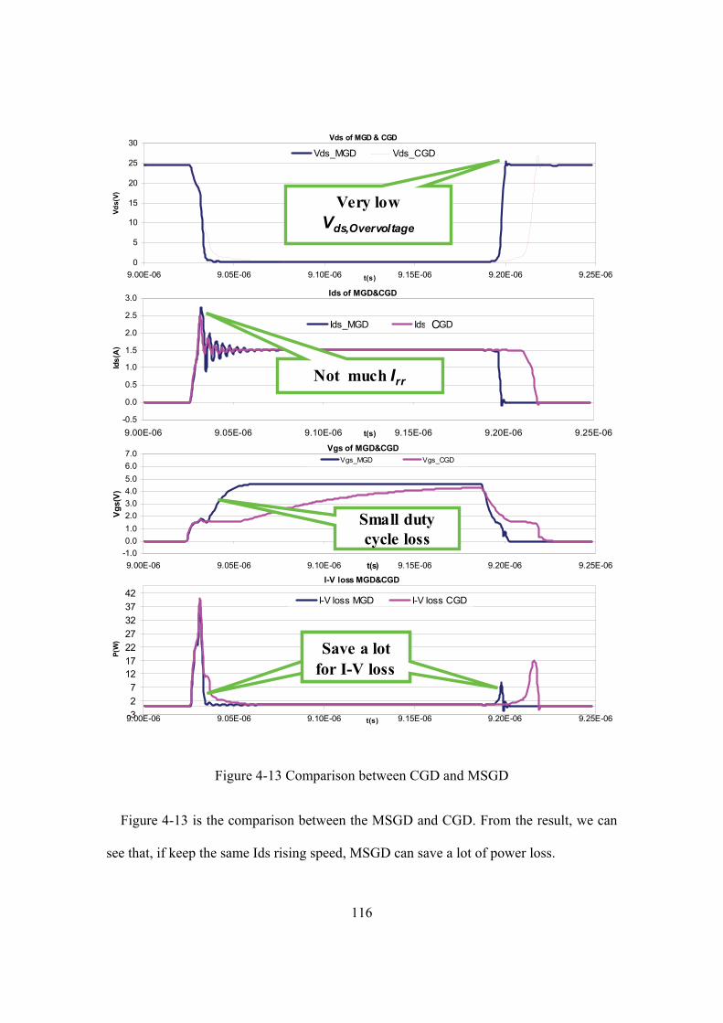
116
Vds of MGD & CGD
0
5
10
15
20
25
30
9.00E-06 9.05E-06 9.10E-06 9.15E-06 9.20E-06 9.25E-06t(s)
Vds(
V)
Vds_MGD Vds_CGD
Vgs of MGD&CGD
-1.00.01.02.03.04.05.06.07.0
9.00E-06 9.05E-06 9.10E-06 9.15E-06 9.20E-06 9.25E-06t(s)
Vgs
(V)
Vgs_MGD Vgs_CGD
I-V loss MGD&CGD
-327
12172227323742
9.00E-06 9.05E-06 9.10E-06 9.15E-06 9.20E-06 9.25E-06t(s)
P(W
)
I-V loss MGD I-V loss CGD
Ids of MGD&CGD
-0.5
0.0
0.5
1.0
1.5
2.0
2.5
3.0
9.00E-06 9.05E-06 9.10E-06 9.15E-06 9.20E-06 9.25E-06t(s)
Ids(
A)
Ids_MGD Ids_MGD
Very low Vds,Overvoltage
Not much Irr
Small duty cycle loss
Save a lot for I-V loss
C
Figure 4-13 Comparison between CGD and MSGD
Figure 4-13 is the comparison between the MSGD and CGD. From the result, we can
see that, if keep the same Ids rising speed, MSGD can save a lot of power loss.
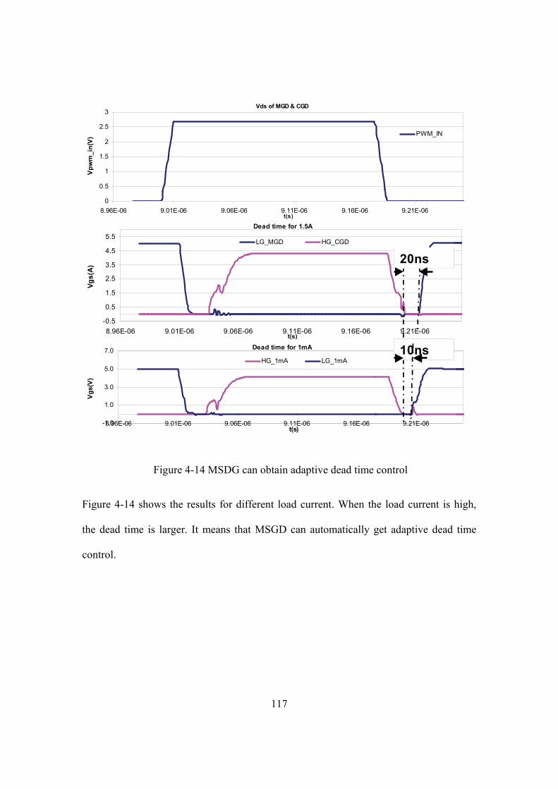
117
Vds of MGD & CGD
0
0.5
1
1.5
2
2.5
3
8.96E-06 9.01E-06 9.06E-06 9.11E-06 9.16E-06 9.21E-06t(s)
Vpw
m_i
n(V
) PWM_IN
Dead time for 1mA
-1.0
1.0
3.0
5.0
7.0
8.96E-06 9.01E-06 9.06E-06 9.11E-06 9.16E-06 9.21E-06t(s)
Vgs
(V)
HG_1mA LG_1mA
Dead time for 1.5A
-0.5
0.5
1.5
2.5
3.5
4.5
5.5
8.96E-06 9.01E-06 9.06E-06 9.11E-06 9.16E-06 9.21E-06t(s)
Vgs(
A)
LG_MGD HG_CGD
20ns
10ns
Figure 4-14 MSDG can obtain adaptive dead time control
Figure 4-14 shows the results for different load current. When the load current is high,
the dead time is larger. It means that MSGD can automatically get adaptive dead time
control.
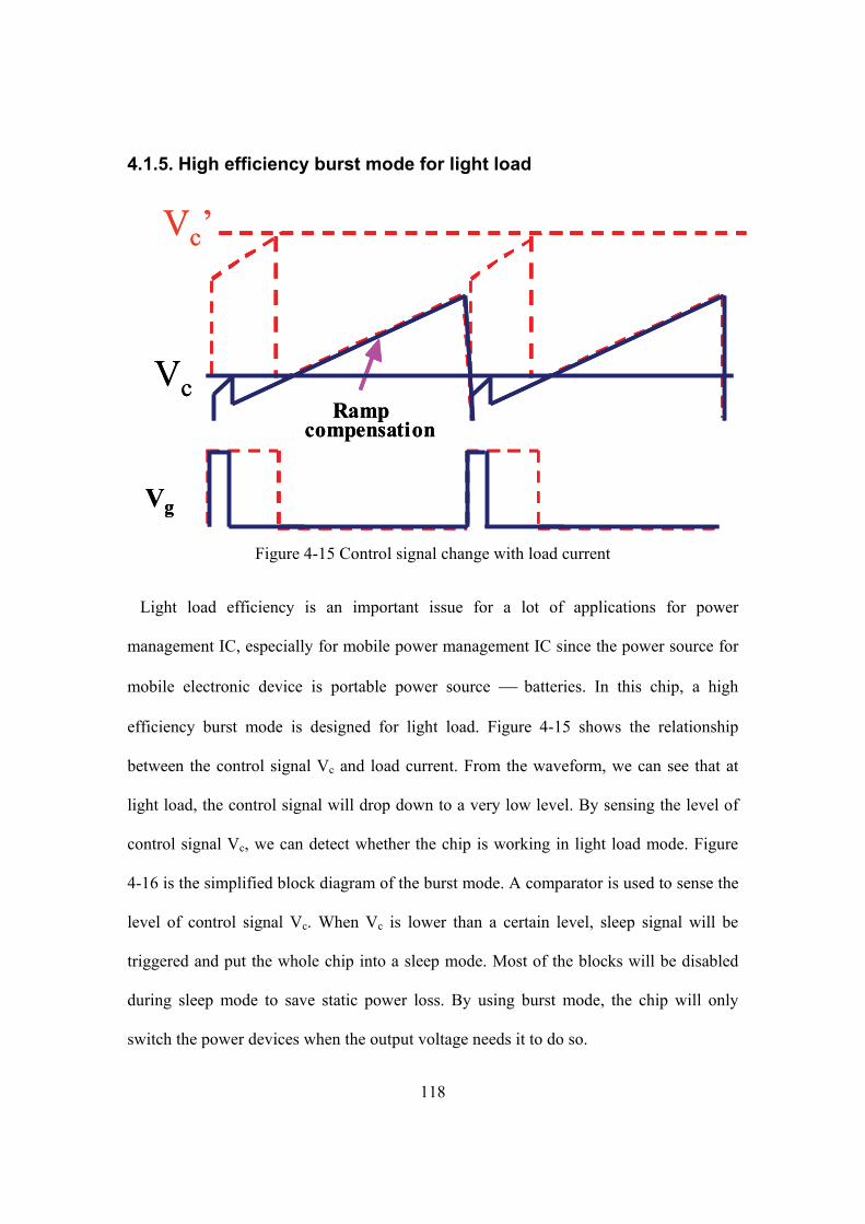
118
4.1.5. High efficiency burst mode for light load
Vc’Vc’
VcRamp
compensation
Vg
VcRamp
compensation
Vg
Figure 4-15 Control signal change with load current
Light load efficiency is an important issue for a lot of applications for power
management IC, especially for mobile power management IC since the power source for
mobile electronic device is portable power source ⎯ batteries. In this chip, a high
efficiency burst mode is designed for light load. Figure 4-15 shows the relationship
between the control signal Vc and load current. From the waveform, we can see that at
light load, the control signal will drop down to a very low level. By sensing the level of
control signal Vc, we can detect whether the chip is working in light load mode. Figure
4-16 is the simplified block diagram of the burst mode. A comparator is used to sense the
level of control signal Vc. When Vc is lower than a certain level, sleep signal will be
triggered and put the whole chip into a sleep mode. Most of the blocks will be disabled
during sleep mode to save static power loss. By using burst mode, the chip will only
switch the power devices when the output voltage needs it to do so.

119
driver
OP Z1(s)
Z2(s)
Vc
Vin Vout
RS
Q
LX
Compensator
PWM modulator
L
CR
RC
Vd
Vg
CS
COVref
driver
OP Z1(s)
Z2(s)
Vc
Vin Vout
RS
Q RS
Q
LX
Compensator
PWM modulator
L
CR
RC
Vd
Vg
CS
CS
COCOVref
Sleep
Vref_burst
Sleep
Vref_burst
Figure 4-16 Simplified block diagram of burst mode
Figure 4-17 shows the difference between the burst mode and normal DCM mode.
During normal DCM mode, the switches will be turned on and off at every cycle. In burst
mode, the switches will only be turned on or off when needed. The efficiency can be
improved a lot especially at very light load.

120
ILVoutVoutVout
ILVoutVoutVout
DCM mode:
Switching every cycle, low efficiency
ILVoutVoutVout
ILVoutVoutVout
DCM mode:
Switching every cycle, low efficiency
ILVoutVoutVout
Sleep mode, low static power
ILVoutVoutVout
Sleep mode, low static power
Switching only when needed, high efficiency
Burst mode:
ILVoutVoutVout
Sleep mode, low static power
ILVoutVoutVout
Sleep mode, low static power
Switching only when needed, high efficiency
ILVoutVoutVout
Sleep mode, low static power
ILVoutVoutVout
Sleep mode, low static power
Switching only when needed, high efficiency
Burst mode:
Figure 4-17 Comparison between DCM mode and burst mode

121
4.2. Noise insensitive and lossless RC sensor
4.2.1. Introduction
Vin
L
ESRL
VoIL
Vin
L
ESRL
VoIL
RsenRsen RsenRsenR
sen
Rse
n
Figure 4-18 External resistor current sensing
Current sensing is a natural part for peak current control. Accurate current sensing is
needed both for control and protection. There are several current sense methods for
power management IC[61][62][63]. Figure 4-18 is the external resistor method. Since the
external resistor can be a high accuracy resistor, the accuracy of this current sensor is
good. However, the additional resistor will cause some additional power loss. There are
three locations for the current sensor resistors. When the resistor is in series with top or
bottom switch, it may have some noise issue since the switching node is quite noisy. If
the resistor is in series with inductor, the noise is small, however, the power loss will
increase.

122
Vin
L
ESRL
VoIL
Vin
L
ESRL
VoILV_isenV_isen
V_isenV_isen
Figure 4-19 Rds_on current sensing
Another sensor method widely used is Rds_on sensor [64][65]. As shown in Figure
4-19, two locations are normally used. Rds_on current sensor uses Rds_on resistor of the
top or bottom switch as the sensor resistor, so it is a lossless current sensor method.
However, since the resistance of Rds_on will change with process, temperature. The
accuracy is not very good. It is also noise sensitive like the external resistor sensor
method.
Rcs Ccs
Gm
R1V_isenVin
L
ESRL
VoIL
VCcs
VL
SGNDPGND
Rcs Ccs
Gm
R1V_isenVin
L
ESRL
VoIL
VCcs
VL
Rcs Ccs
Gm
R1V_isenVin
L
ESRL
VoIL
VCcs
VL
SGNDPGND
~100MHz
Fs=1MHz
Offset voltage~100MHz
Fs=1MHz
~100MHz
Fs=1MHz
Offset voltage
Figure 4-20 Traditional RC current sensing

123
The third widely used method is a lossless RC sensor method shown in Figure 4-20.
We will focus on this method in this section.
V_isen = IL*ESRL *Gm*R1
VCcs
IL
V_isen
VCcs
IL
V_isen
VCcs = IL*ESRL
mV1≈
Figure 4-21 Signal noise ratio is too small for traditional RC current sensor
In traditional RC sensor, time constant of inductor “ LESRL / ” should be equal to time
constant of RC sensor network “ cscs CR * ”, the sensor output signal is LL iESR * . When
LESR is very small, the sensor output signal will be too weak to be detected by other
circuitry. Figure 4-21 is a typical waveform for original RC sensor. The differential
signal across the sensing capacitor Ccs is normally around 1mV. This signal is too small
to be detected by other circuitry due to the large common mode noise everywhere. As
shown in Figure 4-20, there is a lot of noise at Vin node, output node, power ground
PGND and signal ground. Besides these, the offset voltage of the differential Gm block

124
can be several mV. The common mode rejection ratio (CMRR) of the differential Gm
block is not infinite. It is almost impossible to accurate sense the 1mV small signal on the
sensing capacitor Ccs in such a noisy environment. In order to solve this problem, a new
RC sensor is proposed in this section.
4.2.2. Proposed new RC sensor structure
In order to amplify the signal magnitude on the sensing capacitor, two structures are
invented shown in Figure 4-22 and Figure 4-24. In these two new structure, the time
constant of inductor “ LESRL / ” is not equal to time constant of RC sensor network
“ cscs CR * ”. Figure 4-23 and Figure 4-25 are the design equations for structure (1) and
(2). From the equations, we can see that, sensor network time constant “ cscs CR * ” is
times smaller than the time constant of the inductor time constant “ LESRL / ”. If
CSCS
LLCcs CRs
ESRLs
ESRV⋅⋅+
⋅+⋅=1
1
LCSCS ESR
LCR <<⋅CSCS
LLCcs CRs
ESRLs
ESRV⋅⋅+
⋅+⋅=1
1
LCSCS ESR
LCR <<⋅
The signal on the sensor capacitor Ccs will be times larger than original RC sensor. The
differential Gm block can easily catch this signal even in a noisy environment. Another
impedance network is added after the Gm block to make the whole transfer function from
inductor current IL to sensor output V_isen a constant resistor. Figure 4-26 shows the
difference between the new RC sensor and the traditional RC sensor. Since the sensor RC
network is a good low pass filter, which makes this sensor method very suitable for high
frequency switching DC-DC converter. The drawback of this sensor method is that, the

125
tolerance of the ESR of inductor is normally 20%to30%. The accuracy of this sensor
network is not very good.
Rcs Ccs
Gm
R2V_isenVin
L
ESRL
VoIL
VCcs’
VL
C1 R1
Rcs Ccs
Gm
R2V_isenVin
L
ESRL
VoIL
VCcs’
VL
C1 R1
Figure 4-22 New lossless RC sensor structure (1)
Design equations:
112 )( CRRESR
L
l
⋅+=
12 CRCR CSCS ⋅=⋅
1_ RGESRIisenV mLL ⋅⋅⋅=
Figure 4-23 Design equations for new RC sensor structure (1)
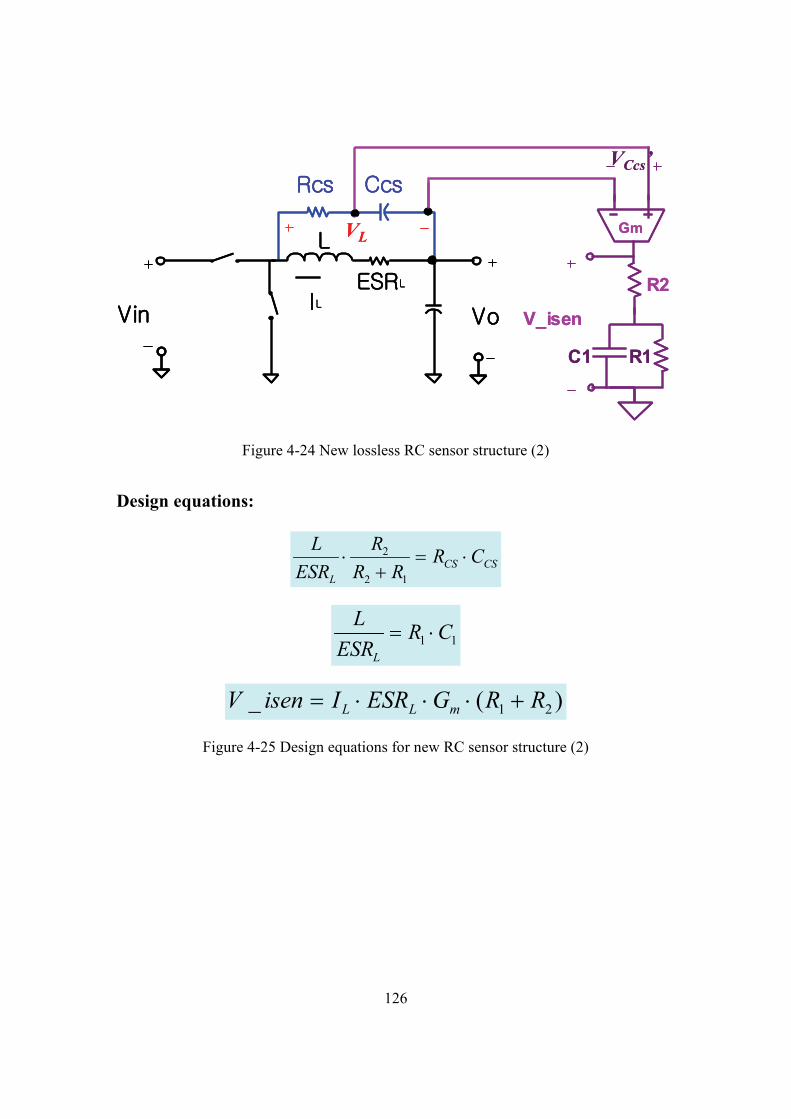
126
Rcs Ccs
Gm
R2
V_isenVin
L
ESRL
VoIL
VCcs’
VL
C1 R1
Rcs Ccs
Gm
R2
V_isenVin
L
ESRL
VoIL
VCcs’
VL
C1 R1
Figure 4-24 New lossless RC sensor structure (2)
Design equations:
CSCSL
CRRR
RESR
L⋅=
+⋅
12
2
11 CRESR
L
L
⋅=
)(_ 21 RRGESRIisenV mLL +⋅⋅⋅=
Figure 4-25 Design equations for new RC sensor structure (2)

127
VCcs
IL
V_isen
VCcs
IL
V_isen
VCcs’
V_isen’
VCcs’
V_isen’
Figure 4-26 Comparison between the new RC sensor and traditional RC sensor
4.2.3. Modeling of the new RC sensor
nHL 300= Ω= mESR L 1.0Ω= KR ORICS 3_
uFC ORICS 1_ =
Ω= KRCS 3 uFCCS 01.0=
Ω= KR 3002 Ω= MR 7.291
pFC 1001 =
Sensor parameters:VVin 12= VVout 1=
AIload 15= MHzfs 1=
VuAGm /10= Figure 4-27 Modeling parameters for the new sensor
A specific application case is selected to model this new RC sensor method. Figure
4-27 shows the parameters used in the modeling.
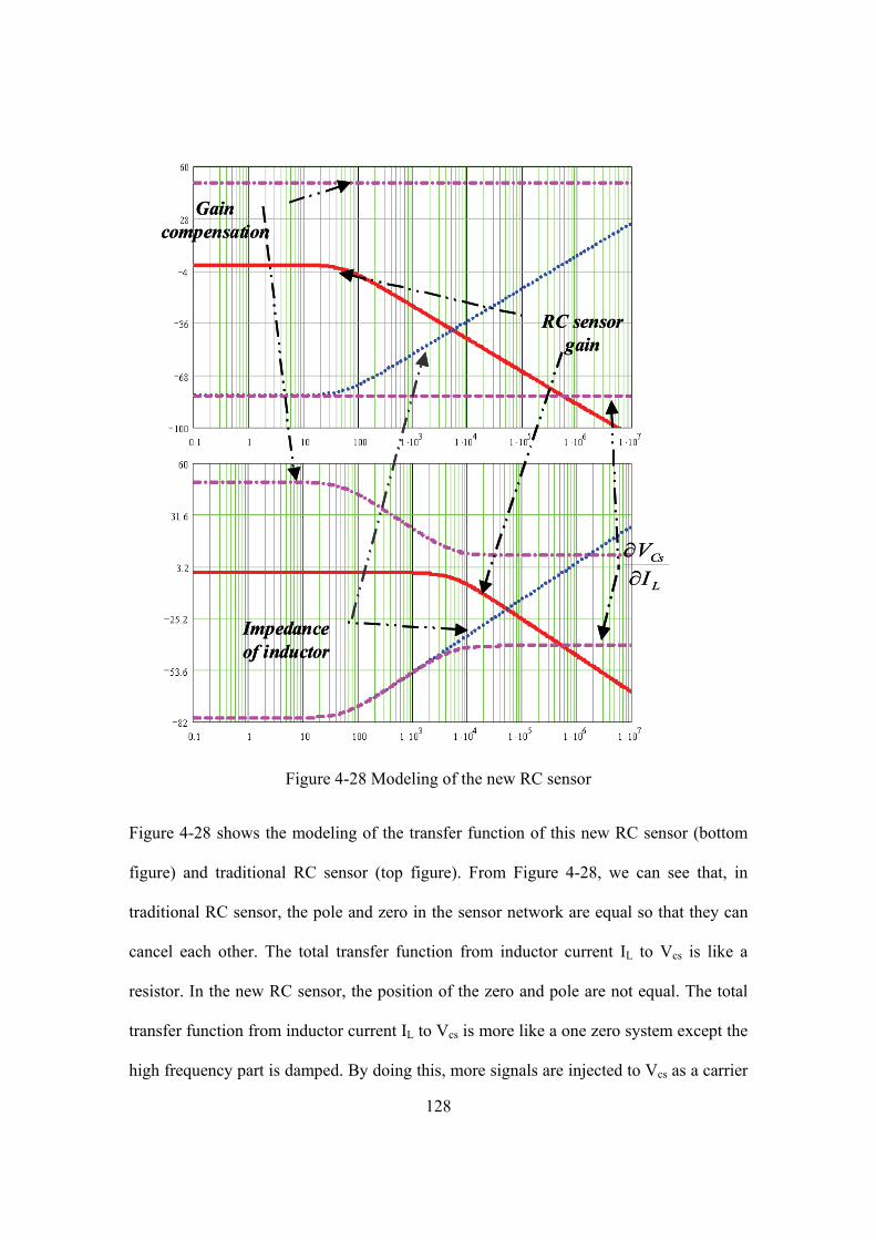
128
Impedance of inductorImpedance of inductor
L
Cs
IV
∂∂
L
Cs
IV
∂∂
RC sensor gain
RC sensor gain
Gain compensation
Gain compensation
Figure 4-28 Modeling of the new RC sensor
Figure 4-28 shows the modeling of the transfer function of this new RC sensor (bottom
figure) and traditional RC sensor (top figure). From Figure 4-28, we can see that, in
traditional RC sensor, the pole and zero in the sensor network are equal so that they can
cancel each other. The total transfer function from inductor current IL to Vcs is like a
resistor. In the new RC sensor, the position of the zero and pole are not equal. The total
transfer function from inductor current IL to Vcs is more like a one zero system except the
high frequency part is damped. By doing this, more signals are injected to Vcs as a carrier

129
signal to help transferring the small signal from Vcs to the output of the Gm block. The
final sensor gains of the new RC sensor and traditional RC sensor are the same except
that pole-zero cancellation is done by two steps in the new RC sensor.
Figure 4-29 shows the results of the modeling case. From this figure, we can see that,
although the signal at switching node is very noisy, the output of the new current sensor
is very clean.
12
13
14
15
16
17
18
19
20
2.8100E-04 2.8150E-04 2.8200E-04 2.8250E-04 2.8300E-04 2.8350E-04
Inductor current
-0.03
-0.02
-0.01
0.00
0.01
0.02
0.03
2.8100E-04 2.8150E-04 2.8200E-04 2.8250E-04 2.8300E-04 2.8350E-04
Vcs in new RC sensor
Vcs in traditional RC sensor
0.35
0.40
0.45
0.50
0.55
0.60
2.8100E-04 2.8150E-04 2.8200E-04 2.8250E-04 2.8300E-04 2.8350E-04
Sensor Output for traditional RC sensorSensor Output for new RC sensor
-10
-5
0
5
10
15
20
25
30
35
40
2.8100E-04 2.8150E-04 2.8200E-04 2.8250E-04 2.8300E-04 2.8350E-04
Voltage at switching point
Figure 4-29 Results of the modeled sensor

130
4.3. Summary
Several novel design concepts are proposed in this chapter for monolithic integration
and high frequency design for switching DC-DC converter. Though these concepts are
derived from a specific monolithic high frequency synchronous buck converter, most of
them are applicable for general switching DC-DC converter.

131
Chapter 5: Experimental Chip Development and Test Results
5.1. Specifications and chip structure
5.1.1. Introduction
In order to study the design issues for monolithic integration of high frequency
switching DC-DC converter, a peak current control monolithic high frequency switching
buck is chosen in this work since peak current control is the most popular control scheme
and buck is a widely used topology in reality.
Figure 5-1is the simplified block diagram of a peak current control buck. There is a
control loop in this system. The control loop can be roughly divided into five parts:
Compensator, PWM modulator, driver, PWM switch and output low pass filter. For
synchronous buck, the rectifier diode is replaced by a transistor to reduce conduction loss.
The basic principle of this control scheme is that: when output is lower than the reference
voltage, control signal Vc will rise up. This signal will compare with the sum of slope
compensation ramp and current sensing ramp and generate a larger duty cycle clock. This
clock signal will be transfer to the gate of the PWM switch by the driver and turn on and
turn off the PWM switch. Since duty cycle is larger, more energy will be transferred to
the output capacitor C and output voltage will rise up to reference voltage. The same
phenomena will happen when output voltage is higher than reference voltage.
In this design, the whole system will be integrated onto a single chip except the output
resonant tank due to the large area needed for large value passive components. All of the

132
issues discussed before will be the design issues for this high frequency buck too. Most of
the new design concepts proposed in the last several chapters are applied in this chip to
verify the correctness of these design concepts.
driver
OP Z1(s)
Z2(s)
Vc
Vin Vout
RS
Q
LX
CompensatorPWM modulator
PWM switch L
CR
RC
Vd
Vg
CS
CO
driver
OP Z1(s)
Z2(s)
OP Z1(s)
Z2(s)
Vc
Vin Vout
RS
Q RS
Q
LX
CompensatorPWM modulator
PWM switch L
CR
RC
Vd
Vg
CS
CS
COCO
Figure 5-1 Simplified diagram of a peak current control buck

133
5.1.2. Pin configuration and pin Description
SW
BOOST
SGND
FB
_SHDN VIN
MODESYN
PGND
TSSOP10
PGOOD VCC
SW
BOOST
SGND
FB
_SHDN VIN
MODESYN
PGND
TSSOP10
PGOOD VCC
Figure 5-2 Pin configuration of the developed chip
Figure 5-2 is the pin configuration of the developed chip. The package for the current
version of this chip is TSSOP10. There are ten pins for this chip. The description is
shown in Table 5-1. The right side pins are most power pins and left side pins are most
analog pins. Most of the energy will go though the right side of the PCB board. The pin
arrangements are designed to minimize the area of the power loops and provide a good
separation between the high power, high noise area and low power low noise analog part.
Most of the power pins have two bondwires to reduce the parasitic inductance and
resistance.

134
Table 5-1 Pin configuration of the developed chip
Model select & synchronize to ext-clkMODESYN
Shutdown the whole chip when at “0”_SHDN
Signal ground, single point to PGNDSGND
Feedback voltage from outputFB
Power good signalPGOOD
Power supply for bottom driverVCC
Power groundPGND
Switching point connected with inductorSW
Input power supplyVIN
Power source for high side driverBOOST
Pin descriptionPin name
5.1.3. Specifications
Typical application diagram
TSSOP10SW
BOOST
SGND
FB
_SHDN VIN
MODESYN
PGND
PGOOD VCC
Vin
VoutTypical application diagram
TSSOP10SW
BOOST
SGND
FB
_SHDN VIN
MODESYN
PGND
PGOOD VCC
Vin
Vout
Figure 5-3 Typical application of the developed chip
Figure 5-3 is the typical application diagram of this chip. Since the top switch is a
NLDMOS device, a voltage higher than the input voltage is needed to turn on this device.
In order to do this, a bootstrap diode and capacitor is connected to boost pin of this chip.

135
When the SW pin goes to ground, input source Vin will charge the bootstrap capacitor to
the input voltage. When the top switch is turned on, SW will rise up to Vin and BOOST
node will be a Vin voltage higher than the input node. In order to prevent the noise in high
power part to feed through to the low power analog part, a single-point connection
method is used in the PCB board layout.
Table 5-2 Specifications of the developed chip
TSSOP10Package
Synchronous, two NLDMOSPower stage
Selectable peak current control or cotangent control
Control scheme
200k-300kHz at 1.5MHzBandwidth
500k-2MHzfsw
0-1.5AILoad
0.8V-0.85xVinVout
3-24VVin
TSSOP10Package
Synchronous, two NLDMOSPower stage
Selectable peak current control or cotangent control
Control scheme
200k-300kHz at 1.5MHzBandwidth
500k-2MHzfsw
0-1.5AILoad
0.8V-0.85xVinVout
3-24VVin
Table 5-2 is the specifications of the developed chip. A wide range of the input voltage
and load current are needed for this chip, which makes the compensator design very
challenging. The maximum frequency of this chip can go up to 2MHz. For this kind of
high switching frequency switching regulator, the loop delay is another concern.
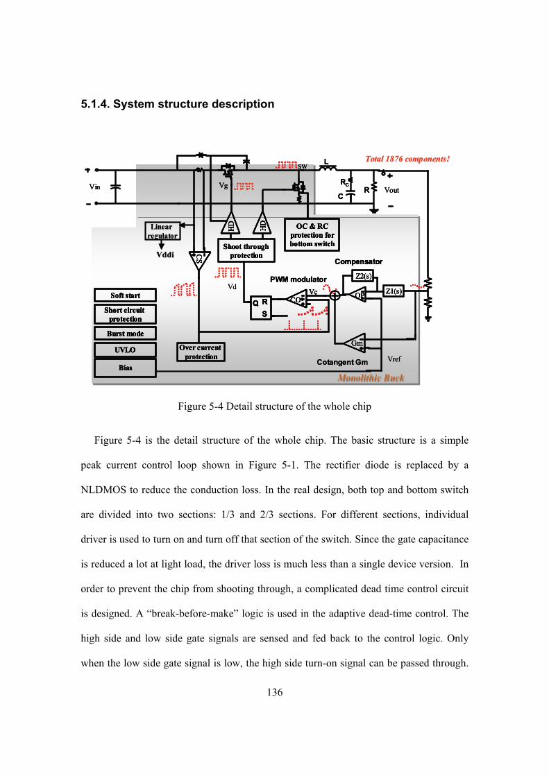
136
5.1.4. System structure description
Monolithic BuckMonolithic Buck
Total 1876 components!
Monolithic BuckMonolithic BuckMonolithic BuckMonolithic Buck
Total 1876 components!
PWM modulatorVc
RS
Q
CS
CO
PWM modulatorVc
RS
Q
CS
CO
PWM modulatorVc
RS
Q
CS
COVc
RS
Q RS
Q
CS
CS
COCO
Linear regulator
Vddi
Linear regulator
Vddi
Vref
Z1(s)
Compensator
OP
Z2(s)
Vref
Z1(s)
Compensator
OP
Z2(s)
Z1(s)
Compensator
OP
Z2(s)
Z1(s)
Compensator
OP
Z2(s)
Over current protection
Bias
OC & RCprotection for bottom switch
Short circuit protection
Burst mode
UVLO
Soft start
Over current protection
Bias
OC & RCprotection for bottom switch
Short circuit protection
Burst mode
UVLO
Soft start
Over current protection
Bias
OC & RCprotection for bottom switch
Short circuit protection
Burst mode
UVLO
Soft start
Over current protection
Bias
OC & RCprotection for bottom switch
Short circuit protection
Burst mode
UVLO
Soft start
Bias
OC & RCprotection for bottom switch
Short circuit protection
Burst mode
UVLO
Soft start
Cotangent Gm
Gm
Cotangent Gm
GmGmGm
Vd
HD HD
Shoot through protection
Vd
HD HD
Shoot through protection
HD HD
Shoot through protection
HD
HD HD
HD
Shoot through protection
L
VoutVin
SW
CR
RCVg
L
VoutVin
SW
CR
RCVg VoutVin
SW
CR
RCVg
Figure 5-4 Detail structure of the whole chip
Figure 5-4 is the detail structure of the whole chip. The basic structure is a simple
peak current control loop shown in Figure 5-1. The rectifier diode is replaced by a
NLDMOS to reduce the conduction loss. In the real design, both top and bottom switch
are divided into two sections: 1/3 and 2/3 sections. For different sections, individual
driver is used to turn on and turn off that section of the switch. Since the gate capacitance
is reduced a lot at light load, the driver loss is much less than a single device version. In
order to prevent the chip from shooting through, a complicated dead time control circuit
is designed. A “break-before-make” logic is used in the adaptive dead-time control. The
high side and low side gate signals are sensed and fed back to the control logic. Only
when the low side gate signal is low, the high side turn-on signal can be passed through.

137
On the contrary, only if the high side gate signal is low the low side gate signal can be
passed through to turn on the low side switch. By using this kind of “break-before-make”
logic, we can prevent the shoot rough problem. Since the ground of the top switch driver
is a floating node SW, we cannot use the global ground as the back gate for those devices
in the high side driver. A NISO tub is used to separate this part from the other part. The
breakdown voltage of this NISO tub to the surrounding area should be high enough to
support the high voltage. The level-shift circuit is a design challenge for this chip. Since
the switching frequency is high up to 2MHz, the speed of level-shift circuit cannot be too
long. A long delay in the level shift will not only cause a phase drop in the control loop,
but also cause a longer dead time. Since the body diode is conducting during dead time,
the large voltage drop on the body diode will cause some additional power loss. With a
longer conduction of body diode, the charge in the diode is going to be larger, which is
going to cause a lager reverse recovery current during switching and so more noise from
power stage. If this noise is not suppressed, it is going to breakdown the power device or
affects the functionality of the analog control circuitry. In order to speed up transient
response, a novel cotangent control scheme discussed in chapter 3 is added to this chip.
Since the input can vary from 3V to 24V, it can’t be directly used as the power supply for
the control circuit. An internal linear regulator is used to generate a 2.7V on-chip power
supply for the control core. As we know, the input port of a buck converter is very noisy
due to the pulsing current going into this port. Any parasitic inductance at the input node
is going to cause some voltage spike at the input port. This input port is used as the input
to the on-chip LDO, which requires that the LDO has a very good line regulation
transient performance. This is sometimes very challenging since the voltage spike at the

138
input side can be several volts and has a frequency up to GHz. It is very difficult to damp
this kind of noise. If this noise is fed through to the output of the LDO, the power supply
for the analog part will be noisy, which is going to impose a high requirement for the
power supply rejection ratio (PSRR) for the analog control circuit. Some other design
features are added to this chip like soft-start, under voltage lockout (UVLO), Output short
circuit protection, high frequency burst mode for light load, over current protection for
both top and bottom switch etc. All of these features are used to protect this chip from
fault operations. The number of the total components of this chip is close to 2000.
5.2. Experimental chip test
The developed buck is fabricated using a 0.5um trenched bipolar-CMOS-DMOS
(BCD) process. The final silicon is packaged and tested in lab. Figure 5-5 shows the
photo of the PCB board. The whole DC-DC converter is only around 2.2cmX2.2cm.
Figure 5-5 Test bench for the developed chip

139
5.2.1. Power on start up
Vin
Vout
LX
Vin
Vout
LX
Vin
Vout
LX
Vin
Vout
LX
Figure 5-6 Tested power on start up when Vin=3V, Vout=1.5V Iload=200mA
Power up is very critical for most of electrical products. Most of the switching
regulators use a soft start structure. In this chip, the reference voltage rises up very slowly
at power up to slow down the inductor current rising speed. Another critical point for
power on start up is the overshoot voltage when the chip begins to go into the steady
state. Figure 5-6 is the test results for the power on start up for this chip. LX is the
switching node. From the waveform, we can see that the output voltage rises steadily up
to the steady state value 1.5V. There is almost no overshoot at the whole process. The
soft-start function and power on reset circuit work well. Another conclusion from this
waveform is that the whole chip is stable in this application case.

140
5.2.2. Steady state
Yellow Trace = VSW - Blue Trace = VboostGreen Trace = Iout - Purple Trace = Vout
20Vin to 3.30Vout @ 200mA
Figure 5-7 Tested waveform for high input voltage
High voltage is a challenge for this chip. When the input voltage is 24V, the maximum
voltage inside the silicon can be almost 30V. If any voltage spike happened inside the
chip, the maximum voltage spike can be even higher. If the voltage spike is higher than
the break down voltage of the power device, which is around 35V, the power device may
be breakdown. Figure 5-7 shows the steady state waveform for high input voltage CCM
application case. From the waveform, we can see that the chip is working well in this
application case. The output is stable at 3.3V.

141
Purple Trace = Vout @ 10mV/DIVGreen Trace = Iout = 1AYellow Trace = SW-Node
9V to 1.60V @1A
Figure 5-8 Tested waveform for low input voltage
High load current is another challenge for this chip. The maxim current for this chip can
be around 1.5A. For such a small package, a large current like 1.5A is a challenge.
Figure 5-8 shows the medium input voltage with 1A load current application case. From
the waveform, we can see that the chip is working fine in this case. The output voltage is
stable at 1.6V.

142
Purple Trace = Vout @ 20mV/DIVGreen Trace = Iout = 10mAYellow Trace = SW-Node24V to 1.60V @10mA
Figure 5-9 Tested waveform for DCM operation
Light load is another extreme condition for switching regulator. During light load, the
transfer function of control loop may be different from the heavy load case since the
inductor is in CCM mode in heavy load case and in DCM mode in light load case. For a
switching buck regulator, the transfer function of the power stage is a two-order system
for CCM. However, it is only a one-order system in CCM when load current is small. A
system may be stable in heavy load CCM case, but may be unstable in light load DCM
case. Another challenge is the wide range of duty cycle. Since the loop gain is related
with duty cycle, the chip can be stable for some duty cycle, but unstable at some other

143
duty cycle case. Figure 5-9 shows the working waveform for a DCM case and small duty
cycle case. From Figure 5-6 Figure 5-7, Figure 5-8 and Figure 5-9 we can see that the
chip can work in a wide working range.
5.2.3. Transient response
3.30VDC to 1.20VDC TransientIout = 0.50A to1.00A
Figure 5-10 Tested waveform for transient response with low input voltage
The main purpose of a switching regulator is to generate a high quality output voltage
under all kinds of application situation. A critical performance specification for most of
the switching regulator is the transient response. Transient response includes line
transient response and load transient response. Both of them include a step-up transient

144
and a step-down transient response. Figure 5-10 shows the load transient waveform with
low input voltage and low output voltage. With a load step from 0.5A to 1A, the output
voltage will only change around 50mV. Figure 5-11 is the transient response test with
high input voltage and low output voltage. The output voltage will change only around
70mV when load changes from 200mA to 1A. The transient response performance of this
chip is good.
24V to 1.60V 200mA to 1.00A
Figure 5-11 Tested waveform for transient response with high input voltage

145
5.2.4. Efficiency and loss break down
Efficiency Vs load Vin=5V [email protected]
0%
10%
20%
30%
40%
50%
60%
70%
80%
90%
100%
0 0.2 0.4 0.6 0.8 1 1.2 1.4 1.6Load current (A)
Effic
ienc
y (%
)
Figure 5-12 Efficiency Vs load current at Vin=5V, Vout=1.5V
Figure 5-12 is the efficiency verse load curve. From the curve, we can see that the chip
can keep a high efficiency at a wide load range. Part of the reason is that we use two-
section device for the chip.

146
0 . 9 3 %
1 . 3 4 %
0 . 9 6 %
1 . 7 5 7 0 %
2 . 3 9 %2 . 5 1 %6 . 4 7 %
2 . 2 3 0 0 %
8 3 . 1 7 %
0.0%
10.0%
20.0%
30.0%
40.0%
50.0%
60.0%
70.0%
80.0%
90.0%
Effi ind
Tswco
n
Bswco
ndrv
bot
drvtop
syndio
Outcap
LDO
Vin5Vout1.5Iload0.4
Figure 5-13 Loss break down at Vin=5, Vout=1.5 and Iload=0.4A
Figure 5-13 is the loss break down of the chip. Since the size of the top switch is not
too much because of the limited silicon area, the conduction loss of the top device is
relatively large. Another phenomenon are the high driver loss. The driver loss is
comparable with device loss, which is specific for high frequency switching regulator. In
order to improve the efficiency, the turn-on and turn-off time for the power switch should
be relatively fast, which will cause a bigger voltage spike on the power switch and a
larger reverse recovery current in the power stage. With this kind of big drive loss, the
efficiency at light load is going to be low at light load. In order to get a high efficiency,
some special control schemes such as PFM, skipping mode, burst mode can be used.
However, those control mode can has a wide frequency spectrum and not suitable for
noise sensitive application.

147
5.2.5. Summary
In order to study the design issues for monolithic integration of high frequency
switching DC-DC converter, a peak current control monolithic high frequency switching
buck is chosen in this work. The chip is fabricated using a trench isolated BCD process.
The power on start up, steady state and transient response are tested. The transient
response of this chip is good. The chip can keep at a high efficiency for a wide load
range.

148
Chapter 6: Conclusion
6.1. Summary
In this work, the modeling and design of a monolithic high frequency synchronous buck
is discussed in details. By doing this chip design, the issues of monolithic integration of
high frequency switching DC-DC converter is investigated. A general analysis method
for frequency response simulation of switching DC-DC converter is developed. Some
novel design concepts are proposed for monolithic integration and high frequency design.
The chip is fabricated and tested finally.
Basically, this work focused on the following topics:
• Proposed a new method ⎯ Periodic small signal analysis based method for
accurate modeling of the frequency response of a switching DC-DC converter
based on SPICE simulator. The basic concept and algorithm are discussed. The
results are accurate comparing with average modeling and experiment results. A
general loop gain design flow based on periodic analysis is proposed for a general
switching regulator.
• Developed a new control scheme ⎯ Cotangent Control (Ctg control) for fast
transient response. Comparing with traditional linear control and existing non-
linear control like LnLc and V2 control, this control has better transient
performance with no effect to steady state performance and better stability
performance. The small signal modeling of this control scheme is discussed. The
stability modeling method ⎯ describing function method is discussed. Finally, a

149
combination of cotangent control with active clamp is studied to get a very fast
transient response for switching regulator.
• In order to implement on-chip compensator, a general small area on-chip
compensator structure ⎯ Active feedback compensator is proposed. By using
miller capacitor and feedback concept, low frequency zero and pole can be
implemented on silicon using a small resistor and capacitor. This structure makes
it possible to implement any kind of compensator on silicon.
• A new concept ⎯ Adaptive compensation is proposed for wide application
range power management IC. The adaptive compensation concept applied for
boost case is discussed in details. By using active feedback compensator, active
compensation can be implemented on silicon easily.
• In order to reduce the reverse recovery current and voltage spike for the power
stage, a new driver structure ⎯ multi-stage gate drive (MSGD) is proposed.
Comparing with conventional gate drive (CGD), MSGD has better noise
performance and efficiency.
• For a certain load, an optimal power device size based on efficiency optimization
is preferred. If the load range is too wide, multi-section device is an option to
improve efficiency at the wide load range. A cycle-by-cycle multi-section device
selection concept is proposed and implemented on this chip.
• Traditional RC sensor has a poor signal-to-noise problem. A new RC sensor is
proposed in this work. This sensor resolved the signal-to-noise problem and make
the RC sensor usable for some noisy environment

150
6.2. Future work
Monolithic integration and high frequency are two trends for modern power electronics.
It is an endless topic in power electronics area like the speed of Pentium processor. Ten
years ago, people were talking about 386, 486, now people are talking about Pentium IV,
G5. The clock frequency is changing from MHz to several GHz. As we can see, hundreds
kHz is a high frequency for current power electronic technology. Several MHz is almost
the highest switching frequency for current technology. New challenges continue to
emerge. At the next several years, the following work may be worthy of study:
New control topology.
o Voltage mode control, peak current control are two most common control
topologies for switching regulator. With the frequency going higher and
higher, more and more issues come out. New control topology is needed
for high frequency monolithic switching regulator
High speed circuit design
o When the switching frequency goes higher, the switching period is going
to be smaller and smaller. The control loop is very sensitive to the delay of
the circuitry. The fastest delay we can get by using current technology is
around 40ns. This is almost 1/5 of the whole switch period if the
switching frequency is 4MHz. If the switching frequency is even higher,
the delay may not be acceptable. Some high-speed circuit design may be
needed for this kind of application.
New circuit block design

151
o As we know, some blocks are frequently used in switching regulator such
as driver, current sensor, level shift and compensator. Though a lot of
topologies for these blocks were proposed by now, we still need some
more advanced design for those blocks. For example, we have a lot of
current sensor circuits, it is still difficult to sense the current in VRD
application. When the switching frequency goes higher, the switching
period is going to be smaller, which requires that the current sensor should
response in a very short time. How to sense the current information
quickly, accurately regardless the input voltage, output voltage, load
current, noise and even temperature is really a tough task. But we still
need to face this problem in the future.
New passive components and power devices
o As we know, passive components and power semiconductor devices are
very important for switching regulator. Passive components are used as
energy storage components for switching regulator. The parasitics like
ESR and ESL impose some bad effect for the performance of switching
regulator. Good passive components with less ESR and ESL are
sometimes the only solution for some critical performance specifications.
Power semiconductor devices are used as power switches in switching
regulator. The parasitic resistance Rdson, parasitic body diode and
parasitic capacitance cause some bad effect to the performance of
switching regulator. With the switching frequency going higher and
higher, the power switches are required to be turned on and off much

152
faster. By using current device technology, the switching loss and noise
caused by turning on or off of the power device may burn the whole chip
or break down the device itself. New technology for power switches is
definitely required for high switching monolithic integration.

153
References
Abstract
[1] Efland, T.R.“The earth is mobile – power”, Power Semiconductor Devices and ICs,
2003. Proceedings. ISPSD '03.2003 IEEE 15th International Symposium on,
Page(s):2- 9
[2] Nick X. Sun, Xiaoming Duan, Xin Zhang, Alex. Huang and Fred C. Lee,” Design of a
4 MHz, 5V to 1V Monolithic Voltage Regulator Chip”, ISPSD’2002 pp. 217 –220.
[3] Katayama, Y.; Sugahara, S.; Nakazawa, H.; Edo, M.; ,” High-power-density MHz-
switching monolithic DC-DC converter with thin-film inductor “, Power Electronics
Specialists Conference, 2000. PESC 00. 2000 IEEE 31st Annual , Volume: 3 , 18-23
June 2000 Page(s): 1485 -1490 vol.3
[4] Richard P.E. Tymerski., “Topology and analysis in power conversion and inversion”,
Ph. D Dissertation, Virginia Tech, April 22, 1988
[5] S. Cuk and R. D. Middlebrook, "A General Unified Approach to Modelling Switching
DC-to-DC Converters in Discontinuous Conduction Mode," IEEE Power Electronics
Specialists Conference Record, 1977
Chapter 1. Introduction
[6] Andrews, N., “The global market for power supply and power management integrated
circuits”, Applied Power Electronics Conference and Exposition, 2002. APEC 2002.
Seventeenth Annual IEEE, Volume: 1, 10-14 March 2002 Pages: 126 - 131 vol.1
[7] Lahiri, K.; Dey, S.; Raghunathan, A.; “Communication-based power management”,
Design & Test of Computers, IEEE, Volume: 19, Issue: 4, July-Aug. 2002 Pages: 118
– 130

154
[8] Lidow, A.; Kinzer, D.; Sheridan, G.; Tam, D.; “The semiconductor roadmap for
power management in the new millennium”, Proceedings of the IEEE, Volume:
89, Issue: 6, June 2001 Pages: 803 - 812
[9] http://www.vdc-corp.com/power/annual/03/br03-14exhibits.html#vol1
[10] Kakumu, M.; Kinugawa, M.; “Power-supply voltage impact on circuit performance
for half and lower submicrometer CMOS LSI”, Electron Devices, IEEE Transactions
on, Volume: 37, Issue: 8 , Aug. 1990 Pages:1902 – 1908
[11] Intel Corporation, “ Voltage Regulator-Down (VRD) design guide”, Apr 2003,
available on www.Intel.com
[12] Sinha, A.; Chandrakasan, A.; “Dynamic power management in wireless sensor
networks”, Design & Test of Computers, IEEE, Volume: 18 , Issue: 2 , March-April
2001 Pages:62 – 74
[13] Musunuri, S.; Chapman, P.L.; “Multi-layer spiral inductor design for monolithic
DC-DC converters”, Industry Applications Conference, 2003. 38th IAS Annual
Meeting. Conference Record of the, Volume: 2, 12-16 Oct. 2003 Pages: 1270 - 1275
vol.2
[14] http://www.volterra.com/vProducts/
[15] http://www.irf.com/product-info/ipowir/indexsw.html
[16] http://www.elecdesign.com/Articles/Index.cfm?ArticleID=4198&pg=2
[17] Klapfish, M.; “Trends in AC/DC switching power supplies and DC/DC converters”,
Applied Power Electronics Conference and Exposition, 1993. APEC '93. Conference
Proceedings 1993., Eighth Annual , 7-11 March 1993 Pages:87 - 91
[18] Ki Hyeon Kim, Jongryoul Kim, Hee Jun Kim, Suk Hee Han, Hi Jung Kim,” A
megahertz switching DC/DC converter using FeBN thin film inductor,” Magnetics, IEEE
Transactions on, Volume: 38, Issue: 5, Sept. 2002 PP: 3162 – 3164

155
[19] Intel Corporation, “ Intel Pentium 4 Processor in the 423 pin package / Intel 850
chipset platform design guide”, Feb 2002, available on www.Intel.com
[20] Pit-Leong Wong, “Performance Improvements of Interleaving VRM with Coupling
Inductors,” Ph.D Dissertation, Virginia Polytechnic Institute and State University,
November, 1990
[21] Papez, V.; Benda, V.; “A wide-band current sensor for power electronics”, Power
Electronics and Variable Speed Drives, 1998. Seventh International Conference on
(IEE Conf. Publ. No. 456) , 21-23 Sept. 1998 Pages:422 - 425
[22] R. B. Ridley, "A New Small-Signal Model for Current-Mode Control", Ph. D
Dissertation, Virginia Polytechnic Institute and State University, November, 1990
Chapter 2. Accurate Control Loop Modeling and Simulation
[23] Middlebrook, R.D.; “Small-signal modeling of pulse-width modulated switched-
mode power converters,” Proceedings of the IEEE, Volume: 76, Issue: 4, April 1988
Pages: 343 – 354
[24] Middlebrook, R.D.; Modeling current-programmed buck and boost regulators,
Power Electronics, IEEE Transactions on, Volume: 4, Issue: 1, Jan. 1989, Pages: 36 –
52
[25] Tan, F.D.; Middlebrook, R.D.; “Unified modeling and measurement of current-
programmed converters”, Power Electronics Specialists Conference, 1993. PESC '93
Record, 24th Annual IEEE, 20-24 June 1993, Pages: 380 - 387
[26] James Groves,“Small Signal Analysis of Nonlinear Systems with Periodic Operating
Trajectories”, Ph.D Dissertation,Virginia Tech, 04 1995
[27] Jason H. Ly, Kasemsan Siri., “Frequency Response Analysis for DC-DC Converters
Without Small-Signal Linearization”, APEC 2003, P1008-1013

156
[28] http://www.transim.com/SS_Overview.html
[29] P. R. Gray and R. G. Meyer, Analysis and Design of Analog Integrated Circuits, 4rd
ed. New York: Wiley, 2001.
[30] Behzad Razavi, “Design of Analog CMOS Integrated Circuits”, McGraw-Hill, 2001
[31] Foty, D.; AC simulation aspects of MOS modeling, Northcon/98 Conference
Proceedings , 21-23 Oct. 1998 Pages:186 - 189
[32]Toshiji Kato, Wataru Tachibana., “Periodic Steady-State Analysis of an Autonomous
Power Electronic System by a Modified Shooting Method”, IEEE TRANSACTIONS
ON POWER ELECTRONICS, VOL. 13, NO. 3, MAY 1998 P522-527
[33] Kenneth S. Kundert, “Introduction to RF Simulation and Its Application”, IEEE
JOURNAL OF SOLID-STATE CIRCUITS, VOL. 34, NO. 9, SEPTEMBER 1999
P1298-1319
[34] Jacob W. van der Woude, Willem L. de Koning, and Yusuf Fuad, “On the Periodic
Behavior of PWM DC–DC Converters” IEEE TRANSACTIONS ON POWER
ELECTRONICS, VOL. 17, NO. 4, JULY 2002, P585-595
[35] Leon O. Chua, Pen-Min Lin, “Computer-Aided analysis of electronic circuits”
Prentice-hall, Inc., Englewood Cliffs, New Jersey, 1975
[36] Vatché Vorpérian, “Fast analytical techniques for electrical and electronic circuits”
Cambridge University press, Cambridge, 2002
[37] Amit Mehrotra, “Numerical Analysis of Electronic Circuits”, August 26, 2003
Chapter 3. “Cotangent Control” Modeling and Implementation
[38] Xunwei Zhou, “Low-voltage High-efficiency Fast-transient Voltage Regulator
Module”, Ph. D Dissertation, Virginia Tech, July 1999
[39] A. Barrado etc., “Stability Analysis of Linear-Non Linear Control (LnLc) Applied
To Fast Transient Response DC-DC Converters.” PESC’03, pp. 1175-1180, 2003

157
[40] A. Barrado etc., “The Fast Response Double Buck DC-DC Converter (FRDB)”,
PESC’03, pp. 1384-1389, 2003
[41] On semiconductor, product datasheet CS5305-D , “Three-Phase Synchronous
Switching Step-Down Controller with Single Wire Current Sharing”, October, 2001
[42]http://www.facstaff.bucknell.edu/mastascu/eControlHTML/Nonlinear/NonLinear2DescFcn.htm
[43]Sridhar, R.,” A general method for deriving the describing functions for a certain
class of nonlinearities”, Automatic Control, IRE Transactions on , Volume: 5 , Issue:
2 , Jun 1960, Pages:135 – 141
[44] Schwartz, C.; Gran, R.;” Describing function analysis using MATLAB and
Simulink”, Control Systems Magazine, IEEE , Volume: 21 , Issue: 4 , Aug. 2001
Pages:19 – 26
[45] Vidal, E.; Poveda, A.; Ismail, M.;” Describing functions and oscillators”, Circuits
and Devices Magazine, IEEE , Volume: 17 , Issue: 6 , Nov. 2001 Pages:7 – 11
[46] Davison, E.;” Application of the describing function technique in a single-loop
feedback system with two nonlinearities, Automatic Control, IEEE Transactions on ,
Volume: 13 , Issue: 2 , Apr 1968 Pages:168 – 170
[47] Kou, S.; Han, K.;” Limitations of the describing function method”, Automatic
Control, IEEE Transactions on , Volume: 20 , Issue: 2 , Apr 1975 Pages:291 – 292
[48] Mees, A.; Bergen, A.;” Describing functions revisited”, Automatic Control, IEEE
Transactions on , Volume: 20 , Issue: 4 , Aug 1975 Pages:473 – 478
[49] Chung, S.C.; Huang, S.R.; Ln, C.I.;” Applications of describing functions to
estimate the continuous and discontinuous conduction mode for a DC-to-DC buck
converter”, Electric Power Applications, IEE Proceedings- , Volume: 147 , Issue: 6
, Nov. 2000 Pages:513 – 519

158
[50] Albert M. Wu and Seth R. Sanders, “An Active Clamp Circuit for Voltage
Regulation Module (VRM) Applications,” Power Electronics, IEEE Transactions on ,
Volume: 16 Issue: 5 , Sept. 2001, Page(s): 623–634
Chapter 4. Efficient, Noiseless Power Stage and Current Sensor Design
[51] Andy Strachan, Doug Brisbin, “Optimization of LDMOS Array Design for SOA and
Hot Carrier Lifetime”, ISPSD’2003
[52] Integrated Systems Engineering, “ISE Integrated Systems Engineering Release 8.5
user manual”.
[53] N. X. Sun*, A. Q. Huang, and F. C. Lee , “0.35 um, 43 uΩcm2 , 6 mΩ Power
MOSFET to power future microprocessor,” Proceedings of the 11th International
Symposium on Power Semiconductor Devices and ICs, pp. 77-80, Toronto, Canada,
May, 1999
[54] Fred Lee and Yuhui Chen, “A Resonant Gate Drive for Power MOSFET,” US Patent
Provisional, LRN 164159PR, October 1999
[55] Richard K. Williams, Bijan Mohandes and Chae Lee, "High-Frequency DC/DC
Converter for Lithium-Ion Battery Applications Utilizes Ultra-Fast CbiC/D Process
Technololgy," Applied Power Electronics Conference and Exposition, 1995. APEC
'95, Conference Proceedings 1995,Tenth Annual Issue: 0 , 5-9 March 1995 Page(s):
322 -332 vol.1
[56] Inaba, C.Y.; Konishi, Y.; Nakamura, M.; Nakaoka, M, .“High frequency PWM
boost chopper-fed DC-DC converters with coupled-inductors”, Power Electronics
Congress, 2002. Technical Proceedings. CIEP 2002. VIII IEEE International, 20-24
Oct. 2002 Page(s):134 –138
[57] Arntzen, B.; Maksimovic, D.;” Switched-capacitor DC/DC converters with resonant
gate drive”, Power Electronics, IEEE Transactions on , Volume: 13 Issue: 5 , Sept.
1998 Page(s): 892 –902

159
[58] Maksimovic, D.;” A MOS gate drive with resonant transitions”, Power Electronics
Specialists Conference, 1991. PESC '91 Record., 22nd Annual IEEE , 24-27 June
1991 Page(s): 527 –532
[59] Kaiwei Yao; Lee, F.C.;” A novel resonant gate driver for high frequency
synchronous buck converters”, Power Electronics, IEEE Transactions on , Volume:
17 Issue: 2 , March 2002 Page(s): 180 -186
[60] B. Murari, F. Bertotti, G.A. Vignola, eds , “Smart Power ICs : technologies and
applications”, Berlin ; New York : Springer, 1996
[61] Papez, V.; Benda, V.;” A wide-band current sensor for power electronics”, Power
Electronics and Variable Speed Drives, 1998. Seventh International Conference on
(IEE Conf. Publ. No. 456) , 21-23 Sept. 1998 Page(s): 422 –425
[62] Pankau, J.; Leggate, D.; Schlegel, D.; Kerkman, R.; Skibiniski, G.;” High frequency
modeling of current sensors”, Applied Power Electronics Conference and
Exposition, 1999. APEC '99. Fourteenth Annual , Volume: 2 , 14-18 March 1999
Page(s): 788 -794 vol.2
[63] Kelley, A.W.; Titus, J.E.;” DC current sensor for PWM converters”, Power
Electronics Specialists Conference, 1991. PESC '91 Record., 22nd Annual IEEE ,
24-27 June 1991 Page(s): 641 -650
[64] Chow, T.P.; Shen, Z.; Pattanayak, D.N.; Wildi, E.J.; Adler, M.S.; Baliga, B.J.;”
Modelling and analysis of current sensors for N-channel, vertical IGBTs”, Electron
Devices Meeting, 1992. Technical Digest., International , 13-16 Dec. 1992 Page(s):
253 –256
[65] Liang, Y.C.; Samudra, G.S.; Hor, V.S.S.;,” Design of integrated current sensor for
lateral IGBT power devices”, Electron Devices, IEEE Transactions on , Volume: 45
Issue: 7 , July 1998 Page(s): 1614 -1616
Chapter 5. Experimental Chip Development and Test Results

160
[66] Haifei Deng; Huang, A.Q.; Yan Ma; “Design of a monolithic high frequency fast
transient buck for portable application”, Power Electronics Specialists Conference,
2004. PESC 04. 2004 IEEE 35th Annual ,Volume: 6 , 20-25 June 2004
Pages:4448 - 4452 Vol.6

161
Vita
The author, Haifei Deng was born in Jiangxi, China on June 1975. He received the
B.S. degree from University of Electronic Science and Technology of China (UESTC),
Chengdu, China in 1997 and M.S. degrees in electrical engineering from Tsinghua
University, Beijing, China, in 2000. He is currently pursuing the Ph.D. degree in power
electronics at the Virginia Polytechnic Institute and State University, Blacksburg. His
research interests include design of power management integrated circuit, control and
modeling of DC-DC switching converter and analog Integrated circuit design.