Embed Size (px)
Citation preview

TRW No 08710-6029-9=l0
gECEIVER pASLLRAND
NAUONAL A HAS -LOCK
RECEIVER FINAL REPORT
Prepared for
NATIONAL AERONAUTICS AND SPACE ADMIN ISTRATION ELECTRONICS RESEARCH CENTER
Cambridge Massachusetts
Under
CONTRACT NO NAS 12-539 LL
N-N7 - 2 8 -3 - -Z$O (ACCES MBER) -(THR ) 2g 7~
I-I
(NASA CR ORTMX ORAD (CATEGORY) I Reproduced by theI CLEARINGHOUSE
for Federal Scientific amp Technical Information Springfield Va 22151
TRW A C O NE S PAC E PA RK R SO] ON 00 8BEACH C AL I F 0R N I A
httpsntrsnasagovsearchjspR=19700018778 2018-05-28T054623+0000Z
08710-6029-RO-00
FINAL REPORT
L-BAND PHASE-LOCK RECEIVER
Prepared for
NATIONAL AERONAUTICS AND SPACE ADMINISTRATION
ELECTRONICS RESEARCH CENTER
CAMBRIDGE MASSACHUSETTS
Under
Contract No NAS 12-539
January f970Sales No 8710 000
Prepared by R V Salcedo Group Head Telecom nunications Dept
Approved byAnager
Tele communications Dept
Approved by
T I Fine Asst Manager For Advanced SystemsGuidance and Navigation Laboratory
CONTENTS
i INTRODUCTION
2 SPECIFICATIONS AND DESCRIPTION 3
3 CIRCUITRY 7
3 1 Preselector 7
3 Z Preamplifier 7
33 Post Selector 7
34 First Mixer 10
35 First IF Amplifier 10
36 Second Mixer and Second IF Amplifier ii
37 Phase Detector and Video Amplifier (Data Channel) 14
38 Local Oscillator Multiplier 14
39 VCXO and Buffer 15
3 10 Reference Oscillator 17
3 ii Bandpass Filter and Amplifier 17
3 iZ Loop Filter and Sweep Circuit 18
3 13 Signal Presence and AGC Amplifier 20
3 14 Power Supply 22
4 RECEIVER TEST RESULTS 23
4 1 Signal Dynamic Range 24
42 VCXO Stability 24
43 Loop Bandwidth Z4
5 BINOR TEST RESULTS 27
APPENDIX A A-I
APPENDIX B B-i
APPENDIX C C-i
ii
ILLUSTRATIONS
plusmn Receiver Front View i
2 Receiver Rear View z
3 Receiver Bottom View 2
4 L-Band Phaselock Receiver 4
5 L-Band Receiver Schematic 6
6 Preselector Module 8
7 Preselector Response 8
8 Microwave Pre amplifier 9
9 Post Selector Module 9
t0 Post Selector Response 10
i1 First Mixer Module 1t
plusmn2 First IF Amplifier 1z
13 First IF AGOC Characteristics 12
14 Monolithic Second Mixer Diagram 13
15 Second Mixer in Flatpack 13
16 Phase Detector Performance 15
17 LO Multiplier Unit 16
i8 VCXO in Flatpack 16
t9 VCXO Character istic s 17
20 Reference Oscillator Module 18
zi BPF and Amplifier Module 19
zz Loop Filter and Sweep Circuit Diagram 19
23 Loop Filter and Sweep Circuit 20
Z4 Signal Presence and AGO Block Diagram Zi
Z5 VCXO Performance Uncompensated 25
26 VCXO Performance Temperature Compensated 25
27 1650 Hz Mode Response 25
Z8 50 Hz Mode Response 26
29 Video Output Waveforms 27
iii
08710-6029-RO-00
i INTRODUCTION
This technical report documents the results to design fabricate
test and deliver a breadboard model of an L-band phase-lock receiver
This project was performed by TRW Systems Group for the NASA Elecshy
tronics Research Center under Contract No NAS-iZ-539 The receiver
is designed to be used in vehicles employing an operational navigation
satellite system although the receiver could be adapted quite easily for a
number of applications To meet the requirements of this project TRW
designed the receiver to employ automatic acquisition tracking and
bandswitching Additionally TRW has integrated and successfully tested
the L-band phase-lock receiver with the BINOR digital processor
Microelectronics is used extensively in this receiver to achieve
low cost and high reliability Microminiaturization is also used in some
of the low-frequency circuits such as the VCXO reference oscillator
and second mixer The balance of the circuitry is implemented with
integrated circuits
Modular packaging is used for the breadboard receiver with the
modules attached to an aluminum chassis Interconnections are made
with coaxial cabling The power supply and the voltage regulator card
are included in the receiver chassis
Photographs of the packaged receiver are shown in Figures 1 2
and 3
Figure i Receiver Front View
1
2 SPECIFICATIONS AND DESCRIPTION
The receiver was designed to have overall electrical performance
as shown in Table I (Exhibit A of the contract) It is a double-conversion
narrowband phase-lock configuration with search acquisition and bandshy
switching capabilities Figure 4 shows the block diagram of the receiver
that meets the performance specifications listed in Table I The nominal
carrier frequency is 1550 MHz 25 kHz with a 5-MHz data channel bandshy
width The receiver threshold is -130 dBm with a 40-dB dynamic range
The differential time delay specification is 15nsec To meet this
fundamental requirement a nonlimiting broadband first If amplifier with
coherent AGC is used followed by a second nonlixniting broadband second
IF amplifier
A phase-lock loop with bandswitching is incorporated allowing a
rapid carrier acquisition prior to data transmittal and correcting any
frequency uncertainties associated with the receivers oscillators or by
doppler
The acquisition bandwidth of 1650 Hz allows the receiver to acquire
the nominal carrier level of -125 dBrn in 038 sec with a reliability equal
or better than 95
After carrier acquisition and prior to data transmittal both the
loop and quadrature channels switch to a 50-Hz noise bandwidth to improve
the signal-to-noise (SIN) ratio by 15 dB in both channels to accommodate
the 9-dB reduction of carrier power during data transmission It also
diminishes the loop sensitivity to the lowest frequency component of the
BINOR code
At the completion of the code and the receiver-processor data upshy
dating interval the carrier is removed allowing the receiver to return
to carrier search mode
A schematic diagram of the L-band receiver is shown in Figure 5
3
SAP
Figure 2 Receiver Rear View
iir
Figure 3 Receiver Bottom View
2
sMgz G0 6 OSTI+TIF
G 70 U
1412Mz AGC
8566
6 NDIF
db 4 - TO IINOR PROCESSOR
X5 MONITOR
plusmn12V C
VCXO a BUFFER 26 864 MHz
v0y
MONITORMOMITORI
plusmnGVDC
LOOP FILTER amp SWEEP
AMPL
MAN
C
DET
K
AMPL WETUKR
CAD
SIGNALrPRE
T
A6C AMPL
L
DRIVE IMNP
s5132T14RES11OLD
DET
T IGA
PRESTNCEINDICATORPSEC
LEVEL PET FLIP-WP 1-201
110 VACCURRENT 4 L a Sigure RELAY
Q - K1 Ka Ks
MOVE SELECTOR
Figure 4 L-Band Phaselock R~eceiver
TABLE I
L-BAND RECEIVER SPECIFICATION
General
Carrier frequency
Receiver carrier acquisishytion threshold
Nominal carrier acquisishytion level
Nominal carrier tracking level
Signal dynamic range
Receiver noise figure
IF bandwidth data channel VCXO stability over
temperature
VCXO sweep range
Probability of lock (-iZ7 dBrn)
Differential time delay
Receiver operating temperature range
Carrier Acquisition
Loop noise bandwidth ZBL
Carrier Tracking (with Modulation)
Loop noise bandwidth ZBL
Carrier modulation loss (mod index-lZrad)
Available carrier power
Loop tracking threshold SN ratio
Power Supply
1550 MHz AZ5 kHz
-130 dBrn
-plusmn25 dBm
-34 dBm
40 dB
60 dB
5 MHz
tiC ppm
-Z5 kHz
0 999 on one-sweep
d15 nsec variation for dynamic range of signal
plusmn0 C to 40C
1650 Hz
50 Hz
88 dB
-356 dBm
+ i5 Z dB
10 Yac 60 Hz
5
3 CIRCUITRY
The circuitry of the receiver uses a combination of TRW microshy
electronics circuits standard integrated circuits and discrete miniature
components for all the filters All TRW microelectronic circuits were
built using sapphire substrate to predict more accurately the uniformity
and performance characteristics Some of the integrated circuitry are
mounted on printed-circuit boards for easier maintenance Each of the
circuits are described below
3 i PRESELECTOR
The preselector is a two-section high-pass filter having an attenushy
ation of 03 dB at L-band frequencies and attenuation of 65 dB at 400 MHz
Figure 6 is a photograph of the preselector module without the cover and
Figure 7 illustrates the frequency response
3 Z PREAMPLIFIER
The preamplifier is a two-stage wideband preamplifier built on a
sapphire substrate of i x 0 5 x 0 040 in (see Figure 8) The preamplishy
fier characteristics are
Gain at L-band 15 dB
Noise figure 4 7 dB
Gain variation 4 100 MHz 05 dB
i dB compression point -I dBm (output)
Power dissipation 96 mW
33 POST SELECTOR
The post selector is a miniature discrete two-pole bandpass filter
that reduces the image frequency therefore improving the SIN ratio
Figure 9 shows the post selector module and Figure 10 the frequency
response
7
Figure 6 Preselector Module
0
-2
-4
-6
-8
-10
-12
-14
-16
-18
-20 1180 1300 1420 1540 1660 1780 1900 2020 2140
MHz
Figure 7 Preselector Response
8
Figure 8 Microwave Preamplifier
Figure 9 Post Selector Module
9
648
0
-2 1550 MHz
RECEIVER CENTER
-6
-8
-10
-12 0
-34
-16
-18 IMAGE FREQUENCY -i
-20 I
-22 I
-24
144 148 1$2 156 160 164 168 REQUENCY (GHz)
Figure tO Post Selector Response
34 FIRST MIXER
This balanced microwave mixer is built on a sapphire substrate
(Figure II) and has the following characteristics
Center frequency- i 6 gHz
Bandwidth too MHz
IF frequency 60 4 MHz
Noise figure lt9 dB
35 FIRST IF AMPLIFIER
The 62-MHz first IF amplifier has 70 dB of gain and 40 dB of AGC
The large allocation of gain for this circuit is intentional to keep the gain
in the 268 MHz second IF amplifier down to 30 dB The gain of the
second IF stages is kept low so that the receiver will not lock onto itself
The first IFcircuit consists of three Philco PA 7600 broadband monoshy
lithic amplifiers and a two-pole bandpass filter inserted between the second
10
Figure it First Mixer Module
and third stages The filter bandwidth is 6 MHz AGC for the first IF is implemented by the combination of a pin diode connected as a variable attenuator between the first and second stages plus controlling the gain of all three stages simultaneously
Figure 1Z is a photograph of the amplifier and Figure 13 illustrates the AGC characteristics
36 SECOND MIXER AND SECOND IF AMPLIFIER
The second mixer and second IF amplifier are combined in one module In the second mixer portion the 62-MHz information signal is converted to 26 866666 M1-z by proper interaction with the 88 866666 MHz reference oscillator Figures 14 and 15 show the circuit diagram and the photograph of the second mixer The mixer is a monolithic circuit that is manufactured by TRW and consists of a two-transistor device with the first transistor being the mixer and the second transistor being the impedshyance matching emitter follower stage The 62-M-z signal is applied to the base of the first transistor while the 88 86 1MHz reference oscillator
it
Figure 12 First IF Amplifier
8I
60shy
5O
g
40
20
lo0 02 04 06 08 10 12 14
AGC IV)
Figure 13 First IF AGC Characteristics
12
0
bull ----- 0( +2V
SIGNAL INPUT (Do -- F_ copyIFOUTPUT
8886 MHz REFERENCE OSCILLATOR
Figure 14 Monolithic Second Mixer Diagram
0Figure 15 Second Mixer in Flatpack
13
signal is injected into the emitter A resistor-capacitor low-pass
network is inserted between the two transistors to attenuate the local
oscillator leakage signal
37 PHASE DETECTOR AND VIDEO AMPLIFIER (DATA CHANNEL)
The receiver uses three identical phase detectors one for the data
channel the second for the loop filter and the third for the coherent
amplitude detector (CAD) of the signal presence circuitry All of these
three-phase detectors are monolithic (Type MC i596G manufactured by
Motorola) The circuit consists of an input differential amplifier driving
a pair of synchronized single-pole double-throw switches The switches
use transistor current mode gates with collectors cross-coupled in such
a manner that a full-wave balanced multiplication results between an
input voltage and the reference switching voltage
Figure 16 shows the output scale factor at 268 MHz in millivolt
radians versus reference signal levels for input signals of -10 to -30 dBw
The data channel phase detector is followed by a monolithic video
amplifier (Type CA30ZSA manufactured by RCA) This circuit is a lowshy
power differential amplifier that converts the differential output of the
phase detector into a single-ended output The frequency response of
this module has been adjusted for a 3-MHz bandwidth into a 1000-ohm load
A complementary follower or other video power stage will be necessary
if the receiver is to drive a 50-ohm line
38 LOCAL OSCILLATOR MULTIPLIER
The local oscillator (L 0) multiplier chain receives its 26 866-MHz
input signal from the voltage-controlled crystal oscillator (VCXO) and
multiplies it by a factor of 60 The i 612-gHz output signal is then fed
to the first mixer as the L 0 signal The L 0 multiplier chain conshy
sists of three transistorized multipliers with multiplication factors of
6 5 and 2
Each transistorized multiplier consists of two stages the first one
operated in Class A mode and the second one in Class B or C Each
multiplier is followed by a filter to eliminate the spurious responses
14
SIGNAL -10 din 900
800
700 SIGNAL -20 d~n
500
n400 0
SIGNAL -3Bdm
200
-30 -20 -10 0
REFERENCE SIGNAL (dim)
Figure 16 Phase Detector Performance
The entire circuit is made with discrete components with the exception of
the XZ filter which is a combline filter built on a sapphire substrate
employing microminiature technology The input and output impedance
of each multiplier is approximately equal to 50 ohms therefore each
unit may be aligned and tested independently A photograph of the entire
L 0 multiplier unit is shown in Figure iM
39 VCXO AND BUFFER
The oscillator circuit is a Colpitt type with emitter feedback A
varicap is used as the voltage-tuned frequency-determining element
The circuitry of the VCXO is a hybrid type packaged in a 38 x 38 flatpack
(Figure 18) The measured VCXO characteristics are shown in Figure 19
Because of the X60 multiplier the frequency variation required of the
VCXO is only 420 Hz from its center frequency of 26 866666 MHz An
emitter follower follows the VCXO to supply four output signals of
- i dBn each for the various circuits of the receiver The stability of the VCXO is better than 5 ppm within the temperature range of 100C to
400 C and the frequency range of interest
i5
Figure 17 L 0 Multiplier Unit
-V
Figure 18 VCXO in Flatpack
16
ROOM TEMPERATURE
+8
0+7 0 gt
gt aCN TER
FREQUENCY
+5
200 400 600 800 200
26866000 26867000
OUTPUT FREQUENCY (MHz)
Figure 19 VCXO Characteristics
3 iO REFERENCE OSCILLATOR
The reference oscillator (XO) is also a Colpitt type The same
masks used in the manufacturing of the VCXO were used for the XO The
difference between the VCXO and the XO is in the tuning elements and
crystal frequency The XO generates an 88 866666-Mqz signal with an
output power of -5 dBm and the stability is t10 ppm within the specified
temperature range The stability of the reference oscillator is masked
by the multiplier factor of the L 0 multiplier chain Figure Z0 shows
the reference oscillator module
3 ii BANDPASS FILTER AND AMPLIFIER
At threshold input the SIN ratio at the second IF amplifier is -30 dB
To improve this condition and to avoid noise saturation of the phase detecshy
tors for the loop filter and AGC circuitry a bandpass filter (BPF) is
placed in the signal path The bandwidth of the BPF is 500 kHz resulting
in an improvement of the SN ratio of 10 dB
17
i4 Figure 20 Reference Oscillator Module
The BPF is a three-pole filter centered at 26866 MHz and followed by a two-stage IC amplifier to compensate for the losses in the filter Figure 21 shows the BPF and amplifier module
3 12 LOOP FILTER AND SWEEP CIRCUIT
A block diagram of the loop filter and sweep circuit module is shown in Figure 2Z The inputs to this module are the 2686 MHz IF signal from the bandpass filter module and the 2686 MHz VCXO signal The output of the phase detector is then filtered in the active loop filter and fed to the VCXO closing the loop when coherency appears
The loop noise bandwidths (ZBL) are determined by the time conshystants associated with the active loop filter Bandwidth switching is accomplished by changing the time constants with miniature relays The relays are operated by the signal presence module
Prior to acquisition the VCXO is swept with a sawtooth waveform of 0 38 sec duration applied to the VCXO drive control voltage The sawshytooth waveform is generated in the active loop filter acting as an integrashy
18
Figure Zi BPF and Amplifier Module
PHASE DETECTOR
ACTIVE LOOP FILTER
K2
__
C
IF SGNALTO VCXO DRIVE
CURRENTLEVL
K4 f K3VCXO
MANUAL ACQUISITION
MONITOR
SOURCE
AMPLIFIER
DTCO
NO
Figure 22 Loop Filter and Sweep Circuit Diagram
i9
tor The current source amplifier supplies either positive or negative
current to the input of this integrator through resistor R The period of
oscillation is determined mainly by the product of R and C
The level detectors Nos I and Z sense the upper and lower levels
of the sawtooth waveform and supply this information to the current source
amplifier through the R-S flip-flop Once either of the two levels has been
reached the flip-flop reverses the jntegrating current A photographof the
loop filter and sweep circuit is shown in Figure 23
313 SIGNAL PRESENCE AND AGC AMPLIFIER
The signal presence and AGC amplifier module performs the followshy
ing tasks
Drives the signal presence light to indicate when the receiver has acquired and locked onto an incoming signal
Supplies a digital signal to the bandswitching relays to change bandwidth from 1650 Hz to 50 Hz when coherence is attained
64O1 69
Figure 23 Loop Filter and Sweep Circuit
20
0 Supplies a coherent AGC voltage to control the gain of the first IF amplifier
Drives the signal strength meter to indicate input level at the receiver
The input signals to this module are the 2686 MHz IF signal and
the 2686 MHz VCXO signal The circuitry consists of a phase detector
connected as a coherent amplitude detector (CAD) followed by a threshold
level detector (pA710) and digital drivers (SGi3Z) for the signal presence
light and bandswitching relays
The CAD also drives the AGC amplifier (LH201 No 2) The gain
of the AGC amplifier is set to cause only a 3-dB change in the second IF
output when the input signal to the receiver varies from -i30 dBm to
-90 dBm Because of scale factor and polarity a separate amplifier
drives the signal strength meter A block diagram of the signal presence
and AGC circuitry is shown in Figure 24
CAD THRESHOLD DETECTORI I
SIGNAL
SIGNALA
TO ELAYS
AGC AMPLIFIER
SIGNAL STRENGTH
- TO FIRST IF
Figure 24 Signal Presence and AGC Block Diagram
21
314 POWER SUPPLY
The supply voltages required to operate the receiver are + 12 -12
+ 6 and -6 V Regulated power supplies are necessary to be able to
track the negative output with the positive output since several operational
amplifiers are used throughout the receiver A dynage module (K iZiZshy
0 5010 50 AKR) dual output dc power supply was selected for the 12 V
with the following specifications
Input 105-125 Vac 50 to 400 Hz
Output 12 V at 05 A each
Regulation combined 005
Ripple 2 mY rms
Tracking t0 005degC
Temperature coefficient 003degC over range
-20degC to + 600C
Temperature operating -20degC to + 7idegC
The +6 and -6 V power supplies are derived from the 12 V supply
in a separate regulator card The 6-V regulator consists of a temperatureshy
compensated zener and an operational amplifier followed by a passing
transistor
22
4 RECEIVER TEST RESULTS
AUI the receiver parameters called out in Table I have been tested
according to the test procedure described in Appendix A Table II shows
those parameters with their respective design goals and the measured
values
TABLE II
RECEIVER TEST PARAMETERS
Test No Parameter
I Carrier frequency
2 Carrier acquisition threshold
3 Carrier acquisition level
4 Carrier tracking level
5 Signal dynamic range
6 Receiver noise figure
7 IF bandwidth D channel 8 VCXO stability
(i0 0 to 400 C)
9 VCXO sweep range
i0 Sweep period
I I Probability of lock at -127 dBm one sweep
12 Differential time delay
03 Receiver operational temperature range
14 Acquisition loop bandshywidth 2 BL
15 Tracking loop bandshywidth 2 BL
Measured Design Goal Values
1550 gHz 25
-130 dBm
-125 dBm
-134 dBm
40 dB
6 dB
5 Ml-z
i0 ppm
416 Hz
0 38 sec
0999
15 msec
10C to 400 C
kHz 1550 gHz 25 kHz
-131 dBm
-125 dBrm
-135 dBm
40 dB
52 dB
5 MHz
22 ppm
420 Hz
038 sec -002 sec
Not directly measured 9 nsec
10 C to 400 C
1650 Hz Approx 1780 Hz
50 Hz Approx 5i Hz
Z3
During the nionth allocated for testing and integration with the
BINOR processor it became evident that the following corrections were necessary
a AGC characteristics
b Temperature compensation of the VCXO
c Lower the output impedance of the video output
Items a and b were corrected but Item c was not considered urgent provided the cable connecting the video output of the receiver
to the BINOR processor was kept short
The following paragraphs clarify the test results for the signal dynamic range VCXO and loop bandwidth measurements
4 1 SIGNAL DYNAMIC RANGE
The receiver has an input dynamic range of 40 dB The gain of the
AGC amplifier was adjusted to maintain the signal output from the second
IF amplifier within 3 dB
42 VCXO STABILITY
The VCXO stability required is 10 ppm over the temperature range of 1oo to 40CC The uncompensated VCXO shows stabilities of 14 ppm and is illustrated in Figure 25
Thermistor-resistance stabilization was used resulting in Z 2 ppm over the temperature and frequency ranges Figure 26 illustrates the
compensated VCXO
43 LOOP BANDWIDTH
The loop bandwidth of the receiver was measured with an input
signal of -124 dBm as described in the test procedure in Appendix A Figure 7 shows the response for the 1650-Hz mode and Figure Z8
depicts the response for the 50-Hz mode
24
-6 +9
+5 +8
0 +4 gt 7
gt r
+3 +6 r-CENTER FREQUENCY CENTER FREQUENCY 26866666 MHz
26866666 MHz
4-2 I 00 +5
S=+40C
4III
26866000 26867000 26866000 268670M0 FREQUENCY (MHz) FREQUENCY (MHz)
Figure 25 VCXO Performance Figure 26 VCXO Performance Uncompensated Temperature
Compensated
1650 Mx MODE
- 124 db INPUT
-4shy
-
-6 1
10 Hz
1 1 1 1 1 1 1 1
100 Hz
I i i i I I
1000 Hz
Figure 27 1650 Hz Mode Response
25
2 -
1
0
50 Hz BANDWIDTH -124 d~m INPUT
-I
-2
-3
-4
-5
-6
-7 1 I Hz
1 1 1 1 10 Hz
I i1 1000 Hz
Figure Z8 50 Hz Mode Response
26
5 BINOR TEST RESULTS
The interface preliminary tests consisted of the L-band transmitter
modulation with the BINOR code or the 3 iZ kHz top tone transmission to
the receiver and processing of the receiver output
After the receiver AGC was adjusted the signal level into the
BINOR processor stayed within the acceptable limits for a wide range of receiver input levels The receiver output coupling capacitor needed to be increased because of an inadequate correlation level on the lowest subshy
frequency tone to the code processor
The receiver-to-processor interface also required close proximity of the two units because of the high output impedance of the receiver and may require receiver changes for impedance matching Printout of the processor output indicated that the system concept and method is practical
and feasible
Figure 29 illustrates the output of the receiver with three different
signal input levels In comparison to the upper two waveforms the sigshy
nal in the bottom portion of the photograph was completely buried within
the noise when adjusted for a minimum signal level but lock-in and proshycessing by the BINOR code processor were easily accomplished with no
errors
Figure 29 Video Output Waveforms
27
APPENDDC A
The test procedure for the L-band phase-lock
receiver is included in this appendix This procedure
explains the tests performed for the fifteen parameters
called out in the receiver specifications The block
diagram test setup the test equipment required and
the test procedure are given for each parameter
A-I
TEST PROCEDURE FOR THE L-BAND PHASE LOCK RECEIVER
Documentation required 1) Schematic L-Band Receiver SK68137
2) L-Band Phaselock Receiver Modules Interconnections SK68138
10 Carrier Frequency Figure A-1 shows one of the suggested RF source
configurations to test most of the receiver parameters
set-up
8614A HP
g Ge
1550 MHz L-Band
Phase Modulator
120 db P
at
arable3MHI
Atten
T
R
HP
Fre uency
I Synthesizer
F
IF Re
2650 P
Oscillator
Synthesizer
EH 122
Pulse Gen
Binor Gen
(or
Figure A- I
V
A-Z
11 Test Equipment Required Frequency Synthesizer HP 51008 Oscillator Synchronizer HP 2650A o Signal Generator HP 8014A o Pulse Generator EH 122 o Binor Code Generator (TRW) L-Band Phase Modulator (TRW) Calibrated Variable Attenuator HP 394A
12 Test Procedure
o Measure the frequency of the 8614A Signal Generator with
5245-L Electronic Counter Hp or equivalent
Make necessary adjustment to the IF reference frequency so
as to read a frequency of 1550 NHz from the Signal Generator o Record frequency reading on test data sheet
20 CARRIER ACQUISITION THRESHOLD 21 Test Equipment Required
RF Test source of Figure A-1 o Power meter HP 431C
22 Test Procedure o Measure RF power available at the input of the receiver with
431C Power Meter HP Add sufficient attenuation following the signal generator soO
as to decrease the available power at the output of the coaxial
calibrated attenuator to -81 dbm when the dial is reading 6 db o Turn the Mode Selector switch of the receiver to-165050 Hz
mode and set the calibrated coaxial attenuator to -145 dbm
output
Increase the RF power to the receiver from -145 dbm until the
receiver shows signs of threshold locking o Record carrier acquisition threshold level on data sheet
30 CARRIER ACQUISITION LEVEL
31 Test Equipment Required o RF Test source of Figure A-1
A-3
32 Test Procedure o Increase the RF power to the receiver to -125 dbm Receiver
should remain locked
40 CARRIER TRACKING LEVEL
41 Test Equipment Required a RF Test source of Figure A-i
42 Test Procedure
o Decrease the RF power to the receiver from -125 dbm to -134 dbm
Receiver should continue in locked condition
50 SIGNAL DYNAMIC RANGE
51 Test Equipment Required
o RF Test source of Figure A-I o Spectrum analyzer HP 851B85518
52 Test Procedure
o Connect spectrum analyzer to the 2nd IFamplifier output pin 5
o Set the RF test source to feed -130 dbm signal to the input
of the receiver o Set the spectrum analyzer in a narrow IFbandwidth to
observe the carrier signal
Increase the input signal to the receiver by 40 db Output
signal observed in the spectrum analyzer should remain
constant within 4 db
60 RECEIVER NOISE FIGURE
61 Test Equipment Required o Noise figure meter
o UHF Noise Source
o 10 db Pad
62 Test Procedure
HP 342A
HP 349A
o Set up equipment as shown in Figure A-2 Notice that the UHF Noise Source has a 10 db pad following removal
of this pad will damape the receiver Pre-amplifier
A-4
62 Test Procedure (continued)
o Adjust the zero and infinity adjustments of the noise figure meter
before taking a reading Noise figure should read between 5 to 6 db Record measurement on data sheet
r _ Noise Figure Meter f UHF Noise 10 db Receiver
I Source Pad Under Test
enHP-3A 349A HP I__--
I Is IFI_) _n_____---
IL
Figure A-2
A-5
3
2
50 Hz BANDWIDTH -124 dm INPUT
0
-1
-2
-3
-4
-5
-6
-7 L I I II
1 Ha 10 Hz 1000 H
Figure 28 50 Hz Mode Response
Z6
5 BINOR TEST RESULTS
The interface preliminary tests consisted of the L-band transmitter modulation with the BINOR code or the 3 iZ kHz top tone transmission to the receiver and processing of the receiver output
After the receiver AGC was adjusted the signal level into the BINOR processor stayed within the acceptable limits for a wide range of receiver input levels The receiver output coupling capacitor needed to be increased because of an inadequate correlation level on the lowest subshyfrequency tone to the code processor
The receiver-to-processor interface also required close proximity of the two units because of the high output impedance of the receiver and may require receiver changes for impedance matching Printout of the processor output indicated that the system concept and method is practical and feasible
Figure 29 illustrates the output of the receiver with three different signal input levels In comparison to the upper two waveforms the sigshynal in the bottom portion of the photograph was completely buried within the noise when adjusted for a minimum signal level but lock-in and proshycessing by the BINOR code processor were easily accomplished with no errors
Figure 29 Video Output Waveforms
Z7
APPENDIX A
The test procedure for the L-band phase-lock
receiver is included in this appendix This procedurq
explains the tests performed for the fifteen parameters
called out in the receiver specifications The block
diagram test setup the test equipment required and
the test procedure are given for each parameter
A-1
TEST PROCEDURE FOR THE L-BAND PHASE LOCK RECEIVER
Documentation required 1) Schematic L-Band Receiver SK68137
2) L-Band Phaselock Receiver Modules Interconnections SK68138
10 Carrier Frequency Figure A-i shows one of the suggested RF source set-up
configurations to test most of the receiver parameters
20 db 8614A HP 1550 MHz L-Band Pad I r9AeHl TO Sig Gen Phase Hl2 AttenW R
Modulator-A
S5100B HP R-2650A HP EH 122
Frequency IF Ref Oscillator Pulse Gen (orI Synthesizer _rSynthesizer Binor Gen
Figure A-1
A-2
11 Test Equipment Required o Frequency Synthesizer HP 5100B
o Oscillator Synchronizer HP 2650A o Signal Generator HP 8014A
o Pulse Generator EH 122 o Binor Code Generator (TRW)
o L-Band Phase Modulator (TRW)
o Calibrated Variable Attenuator HP 394A
12 Test Procedure o Measure the frequency of the 8614A Signal Generator with
5245-L Electronic Counter Hp or equivalent o Make necessary adjustment to the IFreference frequency so
as to read a frequency of 1550 MHz from the Signal Generator o Record frequency reading on test data sheet
20 CARRIER ACQUISITION THRESHOLD
21 Test Equipment Required o RF Test source of Figure A-I o Power meter HP 431C
22 Test Procedure Measure RF power available at the input of the receiver with
431C Power Meter HP o Add sufficient attenuation following the signal generator so
as to decrease the available power at the output of the coaxial calibrated attenuator to -81 dbm when the dial is reading 6 db
o Turn the Mode Selector switch of the receiver to-165050 Hz mode and set the calibrated coaxial attenuator to -145 dbm output
o Increase the RF power to the receiver from -145 dbm until the
receiver shows signs of threshold locking o Record carrier acquisition threshold level on data sheet
30 CARRIER ACQUISITION LEVEL
31 Test Equipment Required o RF Test source of Figure A-I
A-3
32 Test Procedure o Increase the RF power to the receiver to -125 dbm Receiver
should remain locked
40 CARRIER TRACKING LEVEL
41 Test Equipment Required o RF Test source of Figure A-i
42 Test Procedure
o Decrease the RF power to the receiver from -125 dbm to -134 dbm
Receiver should continue inlocked condition
50 SIGNAL DYNAMIC RANGE
51 Test Equipment Required o RF Test source of Figure A-i O Spectrum analyzer HP 851B8551B
52 Test Procedure Connect spectrum analyzer to the 2nd IFamplifier output pin 5
o Set the RF test source to feed -130 dbm signal to the input
of the receiver o Set the spectrum analyzer ina narrow IFbandwidth to
observe the carrier signal o Increase the input signal to the receiver by 40 db Output
signal observed in the spectrum analyzer should remain constant within 4 db
60 RECEIVER NOISE FIGURE
61 Test Equipment Required o Noise figure meter HP 342A
o UHF Noise Source HP 349A
o 10 db Pad
62 Test Procedure o Set up equipment as shown in Figure A-2
Notice that the UHF Noise Source has a 10 db pad following removal
of this pad will damage the receiver Pre-amplifier
A-4
62 Test Procedure (continued)
Adjust the zero and infinity adjustments of the noise figure meter
before taking a reading Noise figure should read between
5 to 6 db Record measurement on data sheet
Noise Figure Meter UHF Noise 10 db V Receiver HP 342A i Source Pad Under Test
349A HP
60 MHz Ist IF 1
Figure A-2
A-5
70 IF BANDWIDTH DATA CHANNEL
71 Test Equipment Required o Power Meter HP 431C
o Signal Generator HP 606C
72 Test Procedure O Reconnect the equipment as shown in Figure A-3 o Sweep manually the input frequency to the Ist IF and record
upper and lower frequencies resulting in 3 db drop from
the 62 MHz center frequency o The difference between the two readings is the bandwidth
of the IF data channel Record the bandwidth on data sheet
st IF 2nd Mixer amp Meter
Amplifier HP 431C
Signa88-866 Ref Osc
Generator 8 HP 606C
Figure A-3
A-6
80 VCXO STABILITY (100 to 40degC)
Data onthis test is available in Engineering Notebook No 8904
Examination of this data can be used to determine the VCXO stability
inlieu of an actual test
81 Test Equipment Required O Test oven
o Frequency counter HP5245L
o Precision power supply EPCO model
82 Test Procedures o Connect equipment as shown in Figure A-4
OVEN
I co IVCXO Frequency 12V Under Counter
Test -
I - - Cwnt~or Voltage
IPrecision PS
Figure A-4
o Vary the temperature of the oven from OdegC to 500C in 10 degree
intervals 0 For each temperature setting vary the control voltage from
+1 to +7 in steps of I volt o Record and tabulate the data
A-7
90 VCXO SWEEP RANGE The receiver has been designed with a sweep range of + 25 kHz The VCXO preceeds a times 60 multiplier chain therefore the actual deviation of the VCXO is 160 of + 25 kHz or + 416 Hz From the data taken inparagraph 8 the scaling factor (approximately
416 Hzvolts) can be obtained The amplitude of the sawtooth waveform sweeping the VCXO determines the sweep range
91 Test Equipment Required o Osci-loscope Tektronix 585
92 Test Procedure o Connect oscilloscope to test point marked TP on the
Loop Filter and Sweep Circuit module o Measure peak-to-peak amplitude of the sawtooth waveform o Calculate and record the sweep range
100 SWEEP PERIOD
101 Test Equipment Required o Oscilloscope Tektronix 585
102 Test Procedure o Connect oscilloscope to test point TP of the loop filter and
sweep circuit o Measure and record the sweep period
110 PROBABILITY OF LOCK (-127 dbm) on one sweep A direct measurement of probability of lock requires several thousands locking operations and a correlation of the compiled data into a single
number
Probability of lock of 0999 becomes very difficult to measure and beyond the scope and capabilities of this program therefore this
test cannot be performed at this time
It is important to notice that the probability of acquisition is a function of several parameters such as signal to noise ratio threshold
sensitivity dampinq factor sweep rate loop bandwidth etc
A-8
It has been demonstrated ()that the smaller the ratio of sweep rate
and loop noise bandwidth the greater is the probability of lock for
a given signal to noise ratio and damping factor
The ratio just mentioned is 0046 for this receiver and it is
obtained as follows
ratio = R = 25xi0 302 = 0046 (1650)2(Bno)2
Figure 3 of the referenced paper shows that the probability of lock
for a 10 db SN and damping factor of 07 is 95 when this ratio
is 012 Therefore the 0046 ratio is an assurance that the
probability of lock is better than 95
120 DIFFERENTIAL TIME DELAY
121 Test Equipment Required o AD-YU 202 Vectorlyzer
o Binor Code Generator
o Binor Processor
122 Test Procedure
o Connect the system as shown in Figure A-5
JP Frazier and J Page Phase Lock Acquisition Study
IRE Trans on Space Electronics and Telemetry page 211
figure 3 September 1962
A-9
Binor CodeGenerator II
600 Binor ohms
code
AD-YU 202 Vectorlyzer
E2 El
Binor I
Processorr_- - -Li0sc
IHFDiv Card LI
Car
H
R-F ~~20db Rcie
Source -
L-Band Phase
Modulator___ Pad - -
Variable Attenuator
Receiver Under TestL _Video
Figure A-5
122 Test Procedure (Continued)
0 Set the Binor Code Generator switches as follows
Mode Switch to CW
Clock Switch to RUN
OUT Switch to NORM
OscSel Switch to INT
Gate Switch to INT
AC Power Switch to ON
deg Adjust the Vectorlyzer per manufacturer procedure on the 0-180 deg scale
bull LFIP supplies a 300 kHz signal from the binor processor oscillator which
is phase locked to the fundamental of the video output of the receiver
providing a noise-free signal for use in the differential time delay A
measurement
A-10
122 Test Procedure (Continued) o Set the RF attenuator for -121 dbm signal to the input of the
receiver and note the phase difference o Increase signal to the receiver to -81 dbm Note the maximum
phase deviation from step above
Multiply maximum phase deviation observed in step above by 925 nsec
per degree The resulting value isthe absolute value of differential
time delay
O
130 RECEIVER OPERATING TEMPERATURE RANGE TEST
131 Test Equipment Required deg Test oven for 100C to 400
o Frequency source set-up as per Figure A-I
132 Test Procedure Place receiver inthe oven and set temperature to 10C After
20 minutes at that temperature check carrier acquisition threshold
O
o Repeat above step for temperature of 20 30 and 400C
deg All the preceeding tests should show a -130 dbm carrier acquisition
threshold or better Record test in data sheet
140 ACQUISITION LOOP BANDWIDTH (2BLs 1650 Hz)
141 Test Equipment Required O Signal Generator HP 8614A
O Oscillator Syncronizer HP 2650A
o Frequency Synthesizer HP 5100B 0 Synthesizer Driver HP 5110B
Dual DC Power Supply HPHarrison 6205B
0 Pin Diode Switch Modulator
Waveteck III Voltage Controlled Generator
o DC Power Supply HP 721A
o Oscilloscope Tektronix 453
Variable Attenuator HP 394A
O 20 db Pad
0
O Wave Analyzer HP 302A
o AC Transistor Voltmeter HP 403A
o Oscilloscope Tektronix 585
A-11
141 Test Equipment Required (Continued) Transmitter Assembly Test Set-up o Connect the transmitter assembly as shown in Figure A-6 o Set the following switches to the indicated position
Tektronix 453 Oscilloscope
Power switch to ON Vertical 2 Vcm DC
o Waveteck III VC Generator
Power switch to Xl
Output selector to Sine wave
o HP 721A Power Supply
Power switch to ON
Voltage adjust pot to -55 VDC (seen on the 453 oscilloscope) o Harrison 6205B Dual Power Supply
Power switch to ON (Modulator power switch should be OFF)
Both Voltage pots to 20 volts DC Wiring should be set up to provide both +20V and -20 volts to the modulator
o Modulator
Power switch to ON
o HP 8614 Signal Generator
Line switch to ON
RF switch to ON
ALC switch to ON Ext FM switch to ON
DBM meter to 0 Attenuation dial to -045 db Frequency dial to 1554 MHz
o HP 5100B HP 5110B Synthesizer
Power switch to operate (both 5100B and 5110B)
Frequency standard switch to INT Frequency selection switch to Local Keyboard Frequency Keyboard switch to 3001005000 Hz Search control switch to Remote
A-12
INSIDE SCREEN ROOMOUTSIDE SCREEN ROOM
HPHarrlson + Modulator 0 Variable ttn Output
6205 B Dua Pwr Sup 20V
0db Port 3PadTo
inpU Attenuator
HP 394A
to Output Receiver
-Video I n shy -
Calib
RF Out
HP 8614A Signal Gen
xt FM Uncal
5 Inc_ - - -
SIF tReAflnu
Y ntsc Tektronix 453
HP 2650 Oscilloscope
Output HP 5100B
Wavetek III VC Gen
SynthesizerAssembly Search --
J output
NOTE Use caution with the
Control Control___ -
ground wiring This generator is operated at an elecated DC level
HP 721A Power Supply
Figure A-6
141 Test Equipment Required (Continued)
o HP 2650A Synchronizer
Power switch to ON
IF Mode switch to EXT
APC switch to ON
Search light should be OFF
Phase meter should be slightly off center This is
accomplished by adjusting the HP 8614A signal generator
frequency
o HP 394A Variable Attenuator
Set the variable attenuator control dial to read 49 db of attenuation (This provides a power into the receiver
of -124dbm)
Allow a 30 minute warm up period before conducting test
Receiver Test Set-up o Connect the receiver assembly as shown in Figure A-7 o Set the following switches to the indicated positions
o HP 403A AC Transistorized Voltmeter
Range switch to 0 db ( 1V RMS full scale)
Function switch to 1 cps - 1 Mc
o Tektronix 585 Oscilloscope
Power switch to ON
Vertical to 1 Vcm DC
o HP 302A Wave Analyzer
Power switch to ON
Scale Value switch to Absolute
Mode selector switch to Normal
o L-Band Phase Lock Receiver (Unit under Test)
Power switch to ON
Allow a 30 minute warm-up period before conducting tests
142 Test Procedure 1650 Hz Noise bandwidth
o The HP 302A Wave Analyzer should be connected to point reg in figure 7 The Mode Selector switch on the receiver should be
in the 1650 Hz AUTO position Set the frequency of the Wavetek Ill oscillator to 250 Hz
A-14
Transmitter Assembly Output from Variable Attenuator
L-Band Phaselock Receiver
Loop Filter and Sweep Circuit
PinLH[OI6 TPI
1
IInput
HP 302A Wave Analyzer
Output
4 input
HP 403A AC Trans-istorized Voltmeter
4 vent-in
Tektronic 585 Oscilloscope
Ficure A-7
Vary the ATTEN control on the Waveteklll oscillator and the
FREQ Keyboard setting of the HP 5100B FREQ Synthesizer until
a reading of -40 db is observed on the HP 302A wave analyzer meter (The Frequency control on the Wave Analyzer will need to be adjusted
for a peak at 250 Hz and the MODE Selector set to AFC) The
proper setting of the FREQ Keyboard will be one of the following
settings 3 0 0 1 0 0 0 50 0 Hz
3 0 0 1 0 0 5 00 0 Hz
3 0 0 1 0 5 0 00 0 Hz
3 0 0 1 5 0 0 00 0 Hz
O Note the signal level in db for various frequencies ranging
from 10 Hz to 2 kHz The procedure for this isto set
the frequency of the Wavetek 111 oscillator to the desired
setting Set the MODE selector on the wave analyzer to NORMAL Adjust the Wave Analyzer Frequency control until a peak
isobserved then replace the MODE Selector to AFC Read the signal
indb directly from the Wave Analyzer meter Compare this data
with figure 3-3 inreference No 1 in order to determine the
damping factor and the loop resonate-frequency
150 TRACKING LOOP BANDWIDTH (2BL) 50 Hz)
151 Test Equipment Required o Same as paragraph 141
Transmitter Assembly Test Set Up 0 Same as paragraph 141
Receiver Test Set Up o Same as Paragraph 141
152 Test Procedures 50 Hz Noise Bandwidth 0 The HP 302A wave analyzer should be connected to point Q
infigure 7 The mode selector switch on the receiver should be inthe 165050 Hz AUTO position Set the frequency of the Wavetek Ill oscillator to 10 Hz
A-16
152 Test Procedures 50 Hz Noise Bandwidth (Continued) 0 Using the procedure of paragraph 142 second item obtain a meter
reading of -10 db at a frequency of 10 Hz Adjust the OUTPUT AMP
pot on the Wave Analyzer until the HP 403A AC transistorized
voltmeter reads 0 db Note The range of this meter is now identical to the range of the
Wave Analyzer This setup may be used down to the frequency
of 3 Hz It should not be used below 3 Hz and at this frequency 1 db should be added to the meter reading At 4 Hz and above
the meter may be read directly o Using the procedure of paragraph 142 third item obtain the signal
level for various frequencies ranging from 3 to 30 Hz The signal should be read in db from the HP 403A voltmeter The
Tektronix 585 scope is provided to aid in the peaking of the signal Compare this data with figure 5-1 in reference No 1
in order to determine the loop resonate frequency o The HP 302A Wave Analyzer should be connected to point reg
in figure 7 The Mode Selector switch on the receiver should be
in the 165050 Hz AUTO position Set the frequency of the Wavetek Ill oscillator to 10 Hz
o Using the procedure of oaragraph 142 second item obtain a
meter reading of -70 db at a frequency of 10 Hz Usini the procedure of paragraph 152 second item calibrate the HP 403A Voltmeter
o Using the procedure of paragraph 142 and 152 third items obtain
the signal level for various frequencies ranging from 3 Hz to 100 Hz Compare this data with figure 3-3 of reference No I to obtain the damping factor
Reference No 1 Theory of Phaselock Techniques as applied to Aerospace
Transponders Floyd M Garner and Steven S Kent
Contract No NAS8-11509 Marshall Space Flight Center
NASA Huntsville Alabama
A-17
APPENDIX B
The modules interconnections diagram is
included to serve as an aid in receiver maintenance
All cabling is coaxial with the exception of the
color-coded power supply wiring meters and
selector switches
B-1
_ 7 643 2
CK PANEL) VIDEO OUTPUT
PRESELECTOR PRE-AMP POST IT IF 2ND MIXER s VIDEO AND SLCF
VIDEOOUPUM (BACKPANEL)
IN INIIGNNAG
STRENGTH MS3IO2ELIOSL-3P P
(FRONT PANEL
N(FON) OFF SWITCH (FRONT)N MLTIPIERMULIPIE -V-12V -GD PAAINALP(FPANEAMD-PL PRESENCE
FUSE HOLDER (BACK) + 3- CAD TEST C
POWER SUPPLY
1212 050050IG REL
L - VCXO AI
+12V LOOP FILTER AND - I aV G O -2 SWE EP C T
R3
-6D VCXCMONITOR -J-I
-6 -6 -12 -12I
MNUAL ACQUISITION CFRONT PANEL) regMODE SELECTOR
(FRONT PANEL) B
4M2v
WIRING OQORCOD
REGULATOR CARD ING RED ___________
-22V BLUE
4 6 ORANGE _ _
A -6VI PURFLEI --__
GND BLACK L BAND PHASELOC
O 1650 MAN shy16 50 HI AUTO-165050 AUTO RCEINTER N
-I-ULES INTERCONNECTIONS
NOTESUNLESSOTHERWSS SPECIFWM
ri I I 5 ~ h~T
APPENDIX C
ALIGNMENT
REQUIRED TEST EQUIPMENT
The following test equipment
for performing these tests
Sweep Generator
CW Generator
Oscilloscope
Attenuator
Spectrum Analyzer
Power Meter
RF Detector-
Synchronizer
Synthesizer
Modulator
Power Supply
Loads
DC Milliamp Meter
Pulse Generator
PROCEDURE
AND TYPICAL TEST SET UP
or its equivalent should be on hand
Jerrold model 900C HP 8690A with 8691A plug-in
HP 606 50 kHz to 65 MHz HP 608 10 MHz to 480 MHz HP 642 450 MHz to 1230 MHz HP 8614A 800 MHz to 2400 MHz
Tektronix 453 Tektronix 585 with (CA type plug-in)
OSM model 20510-3 (3 db) fixed OSM model 20510-6 (6 db) fixed OSM model 20510-10 (40 db) fixed HP 394A (6-140 db) variable HP 8491A - 20 db (20 db) fixed HP 8491A - 10 db (10 db) fixed
HP 851B8551B
HP 431C with 478A thermistor
HP 423A
HP 2650A with 105 3333 MHz crystal
HP 510OB5110B
TRW Bi phase
HPHarr-ison 6205B (dual) (3 each) EPSCO VRS 611 HP 7Z1A
50 ohm OSM 20140P (4 each)
Simpson model 269
EH 122 TRW Binor code generator
C-I
Voltage Controlled Generator- Wavetek model 111
Frequency Counter HP 5245L with 5253 andS54 plug-in
Voltmeter HP 3430A
Noise Figure Meter HP 342A with the HP 349A UHF Noise Source
AC Voltmeter HP 403A (no equivalent)
Wave Analyzer HP 302A (no equivalent)
OUTSIDESCREEN INSIDE SCREEN ROOM
R-- 12V MODULATOR RSNI INTUTF MIABLE ATTNOUTPUT
DUA S P
HP TORECEIVER
Hp8614AISIGNALGENERATOR EXT FM UNCA
IPT RFO U
USECAUTION WITHTHE4535 GROUNDWRING mUSGENERATORIS OPERATED
C ATAN ELECATEDDC LEVEL
OUTPUTHP 510BKII SYNTHESIZER
ASSEMEampy
SEARCH
CONTROL
Figure 1 Transmitter Assembly Test Set-Up
The following test set-ups will be referenced frequently throughout
this procedure
1 1 RIF Test Set-Up
The R F Test Set-Up is illustrated in Figure 4 This set-up will
be used for the following modules
Pre-selector Pre-amplifier Post selector First IF amplifier Second mixer and second IF amplifier Narrowband filter L 0 multiplier
C-a
Each section of this test procedure will specify the connections used
(regthroughreg)or not used and the frequencies and power levels
associated with each connection From this the test equipment may be
easily selected from the provided list
In all sections of this test procedure the RF connections on the test
unit must be terminated into 50 ohms It is recommended that an
attenuator ( 3 to 10 db) or a 50 ohm load be placed on all connectors in
order to insure the proper load impedance and reduce cable effects
It is also recommended that all cables be kept as short as practical
It will be noted that when swept measurements are made then the
sweep generator the REF detector and the oscilloscope are used When
a GW measurement is made the CW generator is used in conjunction
with either the spectrum analyzer or the power meter Allow a 30
minute warm up before conducting tests
SIGNAL GNRIKOSCOPE
GENERATOR ENERATOR
DACPO
C-Figur 2NRUTetStU
SDC POWER
SUPPLIES
DC MILLIAMP
METER
EPSCOVRS 611
VCXODRIVE
UNITUNDER OUTPUT AEN SETUANALYZER
ADDITIONAL OUTPUTS POWER
Figure 3 Oscillator Test Set-Up
1 2- Oscillator Test Set-Up
The Oscillator Test set-up Is illustrated in Figure 3 This set-up
will be used for the following modules
Reference Oscillator VCXO and Buffer
Each section of this test procedure will specify the connections
used (regthrough) or not used and the frequencies and power levels
associated with each connection From this the test equipment may be
easily selected from the provided list
In all sections of this test procedure the RF connectors on the test
unit must be terminated into 50 ohms It is recommended that an
attenuator (3 to 10 db) or a 50 ohm load be placed on all connectors in
order to insure the proper load impedance and reduce cable effects It
is also recommended that all cables be kept as short as practical
Allow a 30 minute warm up before conducting tests
C-4
131
1 3 Transmitter Assembly Test Set-Up
Connect the transmitter assembly as shown in Figure 1
Set the following switches to the indicated position
Tektronix 453 Oscilloscope
Power switch to ON
Vertical Z Vcm DC
Waveteck III V C Generator
Power switch to Xi
Output selector to Sine wave
HP 721A Power Supply
Power switch to ON
Voltage adjust pot to -5 5 VDC (Seenon the 453 oscilloscope)
Harrison 620513 Dual Power Supply-
Power switch to ON (Modulator power switch should be OFF)
Both voltage pots to 20 volts DC Wiring
should be set up to provide both +Z0V and
-20V to the modulator
Modulator
Power switch to ON
HP 8614 Signal Generator
Line switch to ON
RF switch to ON
ALC switch to ON
Ext FM switch to ON
DB2A meter to 0
Attenuation dial to -045 dB
Frequency dial to 1554 MHz
tests only it will be called for inThis equipment is used for specific the procedure if required
C-5
HP 510GBHP 5110B Synthesizer
Power switch to operate (both 5100B and 5110B)
Frequency standard switch to INT
Frequency selection switch to Local Keyboard
Frequency Keyboard switch to 30010000 00 Hz
Search control switch to Local
Pulse Generator
Power Switch to ON
HP 2650A Synchronizer
Power switch to ON
IF Mode switch to EXT
APC switch to ON
Switch light should be OFF
Phase meter should be slightly off center This is accomplished by adjusting the HP 8614A signal generator frequency
HP 394A Variable Attenuator
Set the variable attenuator control dial to read 49 dB of attenuation (This provides a power into the receiver of -424 dBm)
Allow a 30 minute warm up period before conducting test
1 3 Z Transmitter Frequency Adjustment
Connect the counter to the output of the HP 8614A and adjust the
HP 5100B synthesizer frequency until the counter reads 4550 000 MHz
Reconnect the signal generator output to port I of the modulator
133 Power Calibration Procedure
Temporarily remove the 20 dB pad and set the variable attenuator to -10 dB
Connect the HP 431C power meter to point reg (Figure 1)
This equipment is used for specific tests only it will be called for in the procedure if required
c-6
Adjust the variable attenuator on the HP 8614 (oscillator) until -25 dBm is observed on the power meter
Replace the 20 dB pad and add 40 dB to the HP 8614 (oscillator) variable attenuator
The system is now calibrated so that the power input in -dBr to
the receiver is the sum of the HP 394A attenuator reading plus 75
2 SUBASSEMBLY ALIGNMENT PROCEDURES
Ten modules of the L-Band receiver require bench alignment
prior to receiver system test The remaining modules are tested and
aligned utilizing the receiver noise
2 1 Pre-Selector Test Procedure
Utilize the RF test set up of paragraph 1 1 and Figure 2
Connections Approximate requirements
reg input 1 55 GHz at -10 dBn
output 1 55 GHz at -10 dBm
copy (E) and ( un-used
This is a high pass filter It should have an insertion loss of less
than 4 dB and greater than 60 dB loss at 400 MHz The only adjustment
possible in this module is to replace the capacitors or change the length
of the inductors
2 Z Pre-Amplifier Test Procedure
Utilize the RF test set up of paragraph 4 1 and Figure 2
Connections Approximate requirements
reg input 4 55 GHz at -50 dBm
G output 4 55 GHz at -30 dBm
copy D and un-used
DC power +1Z 0 VDC at 10 ma
C-7
2
There is no provision for adjustment of this module It is a wideshy
band preamplifier with only the requirements that the gain at 1550 MHz
be greater than 15 dB that the 3 dB bandwidth be greater than Z0 MHz
(+ and -10 MHz) and that the noise figure be equal to or less than 5 dB
The gain and bandwidth may be tested on this set up however the
noise figure will be tested during the receiver front end alignment
(section 3 2)
CAUTION The preamp contains open circuitry and transistors Do
not touch the substrate or any part in this box
2 3 Post Selector Test Procedure
Utilize the RF test set up of paragraph I 1 and Figure Z
Connections Approximate requirements
G input 45 GHz at -40 dfm
output 1 55 GHz at -40 dBm
un-used
This is a bandpass filter that has an insertion loss of 2 dB or less
and a bandwidth greater than 20 MHz (+ and -40 MHz) at the 3 dB points
The image frequency range (1 665 to 4 675 GHz) must be greater than
20 dB down
The two capacitors should be adjusted with the unit set up in the
swept mode and the CW mode should be used to check the specifications
2 4 1st IF Amplifier Test Procedure
Utilize the RF Test set up of paragraph I I and Figure Z
Connections Approximate requirements
reg input 62 MHz at -80 dBm
output 62 MHz at -10 dBm
Sand reg un-used
AGC input 0 VDC (min gain) to 1 8 VDC (maximum)
DC input +6V at 55 ma
C-8
This high gain amplifier should have a gain of approximately 70 dB
at the center frequency of 62 MHz and a 3 dB bandwidth of 6 MHz (+3 and
-3 MHz) The AGC should have control over a dynamic range of 40 d3
The capacitor (C10 and CI) should be adjusted with the unit in the
swept mode with the AGO voltage set to approximately 1 5 VDC It may
be necessary to select C-19 the coupling capacitor (between C-10 and
C-11) for the proper bandwidth (a larger capacitance causes a narrower
bandpas s)
With the unit in the CW mode apply 26 8 MHz at about -40 dBm
to the input and adjust C-9 and C-16 for a null of the 26 8 MHz signal
at the output Reset the input signal to 62 MHz at -80 dBm and adjust
the AGOC voltage for maximum gain Repeat these adjustments until
satisfaction is achieved
Make a plot of gain versus AGO voltage to insure that the AGC
voltage has a 40 db dynamic range Connect the spectrum analyzer to
the IF output Insure that there is no spurious oscillation while varying
the AGC voltage from 0 to 2 0 volts
Z 5 Znd Mixer and Znd IF Amplifier Test Procedure
Untilize the RF Test set-up of paragraph 1 1 and Figure 2
Connection Approximate requirement
signal input 62 MHz at -50 dBm
O output 4
reference oscillatoinput
r
268 MHz at-4 (35 dB gain)
88 86 MHz at -5
5 dBm
dBm
unused
output 5 Z6 8 MHz at -19 (31 dB gain)
dBm
0 DC power +12 0 VDC at 20 ma +6 0 VDC at 24 ma
This unit should have a gain of approximately 35 db at output 4
and 31 db at output 5 The bandwidth should be 5 MHz at the 3 db points
(+Z 5 MHz and -Z 5 MHz) centered at 26 8 MHz
C-9
Set up the approximate bandwidth first by removing the reference
oscillator input (point ) and setting up the sweep generator at 268 MHz
Adjust C-4 and C-8 for the approximate bandpass Now reconnect the
reference oscillator and set the sweep generator to 62 MHz Adjust
C-4 and C-8 until the desired bandpass is achieved It may be necessary
to select C-5 for the proper bandwidth (a larger capacitance caupes a
narrower bandpass)
With the test set-up in the CW mode and the spectrum analyzer on
the output (4 or 5) insure that the proper gain is achieved at 26 8 MHz
If the conversion efficiency is bad it will be seen by a relatively low
signal at Z6 8 MHz and a relatively high signal at 6Z MHz If this
efficiency is poor it may be required to change the two resistors on pin
5 of the MC 155OG (mixer) Also verify that there are no spurious
oscillations observed on the spectrum analyzer
2 6 Narrowband Filter Alignment
Utilize the RF test set-up of paragraph 1 1 and Figure 2
Connection Approximate requirements
G input 268 MHz at -24 dBm
G output 4 26 8 MHz at -24 dBm
unused
output 5 26 8 MHz at -29 dBm
DC power +12 0 VDC at 20 ma
This narrowband amplifier should have a gain of 0 dB at output
4 and a loss of 5 dB at output 5 The bandwidth should be 500 kHz
(+250 kHz and -250 kHz) at the 3 dB points centered at 26 8 MHz
For swept measurements it may be necessary to increase this power to about -10 dBm in order to have an observable signal However the bandshywidth should be set such that it is correct for a CW test that is performed at -24 dBm
C-10
Connect the test set up in the swept mode and adjust the bandpass
of the filter Adjustments are made by squeezing or separating the turn
of L-3 L-4 and L-5 Next connect the test set-up in the CWmode and
verify the bandpass and gain Also verify that there are no spurious
oscillations seen on the spectrum analyzer
2 7 Reference Oscillator Alignment
Utilize the oscillator test set-up of paragraph 1 2 and Figure 3
Connections Approximate requirements
)unused
output unit 1 88 866666 MHz at -5 dBm
unit 2 amp3 88 861666 MHz at -5 dBnm
DC power -4Z 0 VDC at 3 ma
Adjust C-3 for the proper frequency as observed on the counter
Monitor the output on the power meter and observe the -5 dBm on the
power meter It may be necessary to add a resistor (45K or greater)
from pin 10 of the flatpack to ground in order to increase the output
power Monitor the output on the spectrum analyzer and verify that
there are no spurious oscillations
Repeat the above tests with the unit in an environmental temperature
chamber Over the temperature range of +400C to +400C the frequency
change should be less than 10 PPM (886 Hz)
2 8 VCXO and Buffer Alignment
Utilize the oscillator test set-up of paragraph 4 2 and Figure 3
Connections Approximate requirements
VCXO drive 3 VDC to 9 VDG nominal to 6 VDC
Q and outputs 26 866666 MHz at -11 dBm
D DC power -Z 0 VDC at 16 ma
NOTE All tests on this device are performed with the oscillator output (OUT) connector connected to the buffer input (IN) connector through a short piece of coaxial cable Any one of the buffer outputs (output 4 thru 4) are then measured
C-l1
Select R-11 to the 9 05 K ohms
Set the VCXO drive voltage to 6 0 VDC and adjust C-3 until the
proper frequency (26 866666 I-z) is observed on the counter Monitor
the outputs (i thru 4) with the power meter and verify that they are at
-11 dBm It may be necessary to add a resistor (15 K or greater) from
pin 10 of the flatpack to ground in order to increase the output power
Make a graph of the frequency versus VCXO drive voltage of 3 OV to
9 OV Verify that the slope of this curve (VCXO scale factor) is about
400 Hzvolt Connect the output to the spectrum analyzer and verify that
there are no spurious oscillations
Repeat the above tests with the unit in an environmental temperature
chamber Select R-11 until the change in frequency between the tempershy
ature of 40 0C and 400C at any VCXO drive voltage (3 CV 6 0V or 9 OV)
is less 10 PPM (268 Hz)
Repeat the above tests until the satisfaction is achieved
2 9 L 0 Multipher (X 60) Alignment
CAUTION Due to the non-linear elements and the high frequencies associated with frequency multipliers it is not recomshymended that this adjustment be performed outside of the factory Should this procedure be attempted it is essential that it be performed under laboratory condishytions utilizing the proper test equipment and pershysonnel that have extensive knowledge of RF techniques and experience with Varactor multiplier adjustment This document is written as a guide to the qualified technician not as an absolute step-by-step procedure
2 9 1 Preliminary Set Up Considerations
The multiplier should be energized with +iZ 0 volts DC (the case
is ground) The typical DC current for the whole unit is about 30 ma
therefore a current limited supply at about 50 ma should be used
The unit is composed of 4 parts 3 RF cards and one comb-hne
filter (see Figure 4) Preliminary adjustments on each of the 3 cards
should be made individually These adjustments are discussed in
sections Z 9 Z 2 9 3 and 2 9 4 The set-up for each of these sections
is to solder on a coaxial cable to the input and output of the card having
C-1Z
removed the original connection and terminate these cables into 50 ohm
impedance It is recommended that each coax be kept short and that a
50 ohm attenuator (3 to 10 db) be placed as close to the card as possible
SEE NOTE -- --BELOW ---
X2 X5 X2 MULITPLIER MULITPLIER MULTIPLIER
CARD CARD CARD INPUT OUTPUT OUTPUT OUTPUT
IN PUTTOUPU COMBLINEINPUT[ FI[Z]PLTER
INPUT OUTPUT INPUT OUTPUT
GND DC INPUT
NOTE DO NOT SOLDER TO THE COMB-LI NE (MICRO-STRIP) FILTER CONDUCTIVE EPOXY MUST BE USED HERE
Figure 4 Multiplier Configuration
Final adjustment of the unit must be accomplished with the unit
completely assembled _ and that the input and output connectors be
terminated into 50 ohms It is recommended that an attenuator
(3 to 10 db) be placed on the input and output connector in order to insure
proper impedance matching and reduce cable effects
NOTE DO NOT solder to the comb-line (micro-strip) filter Conductive epoxy must be used here
C-13
The typical test set up is illustrated in paragraph 1 1 and
Figure 2 This set-up should be used whether the test unit is only one
card or the entire multiplier unit The only precaution necessary is that
the test equipment will supply the required input frequencies and power
levels and that the test equipment is linear at the output frequencies and
power levels These data are given in Table 4
Table I InputOutput Requirements
Input at Connection Output at Connection G
Unit Frequency Power at PT A Frequency Power at PT BMHz dbm (50 ohmF MHz drn (50 ohmT
X6 269 -10 161 -95
X5 161 -95 806 0
XZ 806 0 1612 +10 0
X60 269 -40 1612 +100
Connection Approximate Requirements
Bampa)Unused
DC Power +12 0 VDC at 30 ma
2 9 2 X6 Multiplier Card Adjustment
The test set-np should be connected in the CW mode utilizing the
spectrum analyzer as an indicator Tune C5 C8 C10 C12 and C11
for a maximum signal at 161 MHz Be sure that the signals at 133 MHz
(X5 mode) and 187 MHz (X7 mode) are as low as possible
The test set-up should now be changed to the swept mode and the
same capacitors adjusted until a pleasant band pass is observed that is
about 7 MHz wide at the 3 dB points (relative to output frequency)
Repeat the previous two paragraphs until a satisfactory bandpass
is achieved and all spurs and harmonics noted in the first paragraph
are about 60 dB below the carrier
C-14
Next connect the test set-up in the CW mode with the power meter
as an indicator The power out should be -10 dBm If this is not satisshy
factory adjust R2 or Ri until satisfaction is achieved
Again repeat all previous paragraphs of this section until satisfaction
is achieved
It should be noted that C5 adjusts the resonance of the input circuit
whereas C8 C10 and C12 each adjust the resonance of one pole of the
3 pole filter in the output circuit Adjustment of C11 changes the impedance
loading that the filter sees and thus it adjusts the filters coupling and
shape Adjustment of RZ and R1 change the transistors bias voltage so
that the transistor Q will be operating at its most optimum point (class B)
for multiplication
Z 9 3 X5 Multiplier Card Adjustment
The test set-up should be connected in the CW mode utilizing the
spectrum analyzer as an indicator Tune C18 CZI CZ5 CZ7 and C26
for a maximum signal at 806 MHz Be sure that the signals at 644 MHz
(X4 mode) and 965 MHz (X6 mode) are as low as possible
The test set-up should now be changed to the swept mode and the
same capacitors adjusted until a pleasant bandpass is observed that is
about 35 MHz wide at the 3 dB points (relative to output frequency)
Repeat the previous two paragraphs until a satisfactory bandpass
is achieved and all spurs and harmonics noted in the first paragraph
are about -47 dB below the carrier
Next connect the test set-up in the OW mode with the power meter
as an indicator The power out should be at 0 dBm If this is not
satisfactory adjust R4 or R7 and R9 or R8 until satisfaction is achieved
Again repeat all previous paragraphs of this section until satisshy
faction is achieved
It should be noted that C18 adjusts the resonance of the output
circuit of the input (161 MHz) amplifier QZ R4 and R7 adjust the bias
voltage of this class A amplifier and thus adjusts its gain R9 and RI0
adjust the bias voltage of the multiplying transistor Q3 so that it will be
C-15
operating at its most optimum point (class B) for multiplication CZI
CZ5 and C27 each adjust the resonance of one pole of the 3 pole filter
in the output circuit C26 adjusts the loading impedance seen by the
filter thus adjusting the filters coupling and shape
Z 94 XZ Multiplier Card Adjustment
The test set-up should be connected in the CW mode utilizing the
spectrum analyzer as an indicator Tune L9 and C36 for a maximum
signal at 1612 MHz Be sure that the signals at 806 MHz (XI mode)
and Z418 MHz (X3 mode) are as low as possible
L9 is adjusted by changing the length of the coil This usually
involves unsoldering the coil changing it then resoldering it back in place
repeated soldering may damage the circuit board therefore this procedure
should be done as few times as possible
The test set-up should now be changed to the swept mode and the
same elements adjusted until a pleasant bandpass is observed that is
about 140 MHz wide at the 3 db points (relative to output frequency)
Repeat the previous two paragraphs until a satisfactory bandpass
is achieved and all spurs and harmonics noted in the first paragraph are
about 27 db below the carrier
Next connect the test set-up in the GW mode with the power meter
as an indicator The power out should be equal to or greater than +10 dbm
If this is not satisfactory adjust R13 or R1Z and R16 or R17 until satisshy
faction is achieved
Again repeat all previous paragraphs of this section until satisshy
faction is achieved
It should be noted here the L9 adjusts the resonant point of the
output circuit of the input (806 MHz) amplifier Q4 whereas R13 and
R1Z adjust the bias voltage of this amplifier (class A) R16 and R17
adjust the bias voltage for the multiplying transistor Q5 such that it is
operating at its optimum point (class B) for multiplication C35 adjust
the output tank of this circuit
c-16
2 9 5 Total Multiplier Alignment
It is essential that the technician follow three basic principles when
adjusting the total unit
First Always understand exactly what he is adjusting in terms
of circuit element electrical element and expected response
i e C10 adjusts the center pole of the 160 MHz filter and
should cause the response to increase in amplitude and become
flat when properly adjusted
Second- Only make very small changes at any one time A large
change could cause an erroneous indication i e a large
change in C21 could cause the X5 multiplier to operate better
as a X4 and the swept bandpass look improved however the
change in output frequency would go un-noticed
Third Always use proper ftF techniques
The unit should be set up in the swept mode and the following
adjustments performed while looking for the highest-most pleasant
looking bandpass
1 Adjust the two capacitors of the comb line (microstrip) filter along with C36 This is to align the output filter and the output tank of the X2 multiplier card
2 Next adjust the input tank C5 to insure input impedance matching
3 Next adjust CZ7 CZ5 and CZ to insure the alignment o of the 800 MHz filter
4 Next adjust C12 CI0 and C8 to insure the alignment of the 460 MHz filter
5 Then adjust C8 to insure the alignment of the 160 MHz
amplifier
6 Steps 1 through 5 should be repeated
7 Then adjust coupling capacitor C26 to flatten out and widen up the response C27 will need to be adjusted to bring the filter pole back to its proper position
C-17
8 Then adjust coupling capacitor C11 to flatten out and widen up the response CZ will need to be re-adjusted to bring the filter pole back to its proper position
9 Again repeat steps I through 5
This procedure should be repeated until a satisfactory response is
noted
The test set-up should then be set up in the CW mode utilizing the
spectrum analyzer as an indicator Insure that the spurs and harmonic
frequencies are all about 45 dB below the carrier The 806 MHz harmonic
may be only about 30 dB below the carrier - for this frequency this is an
acceptable level
The test set-up should then be set up in the CW mode utilizing the
power Meter as indicator The power out must be equal to +10 dBm If
these last two requirements are not satisfactory then all steps of this
section should be repeated until satisfaction is achieved
It should be noted that between the output of the X6 multiplier card
and the input of the X5 multiplier as well as on the input of the X2
multiplier card are provisions for the installation of a resistive 7t type
attenuator The application of the attenuator is left to the judgement of
the technician Should an attenuator be placed at either of these points
then it should be calculated for a characteristic impedance of 50 ohms
2 10 6V Regulator Alignment
Connect +1Z 0 volts and -12 0 volts to the regulator card Load
the +6 volt and -6 volt output with 4Z0 ohm 1Z watt resistor This will
give a current of approximately 50 ma Connect the DC voltmeter to
+6 volt output and adjust R-9 for 6 000 VDC Connect the DC voltmeter
to the -6 volt output and adjust R-Z for -6 000 VDC
3 SYSTEM TESTS
It is assumed that all of the modules have been previously tested
as illustrated in section 2 of this procedure that the receiver has been
assembled per drawings SK 68137 (Receiver Schematic) and SK 68138
(Receiver Modules Interconnections) the Power switch is ON the Mode
C-18
Selector switch is to 1650 Hz manual and that the system has had a
30 minute warm up period
3 1 Power Supply and Regulator Adjustment
Connect the voltmeter to the +12 volt input to the regulator card
Adjust the power supply for +12 00 volts
Connect the voltmeter to the -42 volt input to the regulator card
Verify that this voltage is -42 00 =h 06 volts
Connect the voltmeter to the -6 volt output of the regulator card Adjust R-2 for -6 000 VDC
Connect the voltmeter to the +6 volt output of the regulator card
Adjust R-9 for +6 000 VDC
Adjust R-15 until the VCXO monitor meter swings about mid range
Adjust R-16 until the signal strength meter reads 0
3 2 Receiver Front End (RF) Alignment
Connect a power meter through a 10 dB attenuator to the output of
the L 0 multiplier Adjust the input capacitor (C-5) of the multiplier
for maximum power out Reconnect the L 0 output to the 1st mixer
Set up equipment as shown in Figure 5 Notice that the UHF noise
source is connected to the receiver through a 10 dB pad removal of this
pad will damage the receiver pre-amplifier
NOISE FIGURE METER UHF NOISE 10 dB RECEIVER
P UNDER TESTSOURCEHP 342A 60 MHz HP 349A S IF 0PUT
Figure 5 Front End Alignment
C-19
Adjust the zero and infinity adjustments of the noise figure meter
before taking a reading
Adjust the following items for minimum noise figure
The output (Bandpass) filter of the L 0 multiplier
The length of cable between preselector and pre-amp
The length of cable between pre-anp and post selector
The length of cable between post selector and 1st mixer
The final noise figure should be less than 6 dB Return the system to its normal configuration (paragraph 3 0)
3 3 System Alignment
3 3 i Reference Oscillator Adjustment
Connect the counter to the output of the reference oscillator
Adjust C-3 for a frequency of 88 866666 MHz
Return the system to its normal configuration
3 3 Z Video Amplifier Gain Adjustment
Connect the oscilloscope to the video output Adjust R13 of the
phase detector and video amplifier for maximum noise signal
3 3 3 VCXO Sweep Adjustment
Connect the oscilloscope to TP-plusmn on the loop filter and sweep
circuit Adjust the following controls on the loop filter and sweep circuit
Until the wave form conforms to Figure 6
R13 - Symmetry Control
R16 - Lower Voltage Control (+55V)
R17 - Upper Voltage Control (+83V)
R3 - Period Control ( 76 plusmn 04 Sec)
C-20
DC 76 004 SEC shy+55 +55-[C
Figure 6 VCXO Drive Waveform on TP i
3 3 4 AGC Adjustment
Insure that there is no RF input to the receiver On the signal presence and AGOC amplifier connect the voltmeter to the CAD Test
connector and adjust R-11 CAD zero for zero volts Next connect
the voltmeter to the AGOC output of this amplifier and adjust R-27 AGC
level for a DC voltage of 1 80 VDC Next connect the voltmeter to
pip 6 of the LH Z01 3 in this amplifier and adjust R-35 AGO meter
for zero volts
3 3 5 Threshold Adjustment
Connect the transmitter assembly of paragraph 1 3 and Figure 3
to the receiver input The power at point reg (Figure 3) should be set
to -120 dBm and the connections at points reg and-Vcopy should beshoud beopen
On the signal presence and AGC amplifier connect the voltmeter
to the CAD test connector Increase the variable attenuator until the
receiver locks up Adjust C1 of the Signal Presence and AGC Amplifier
until a maximum positive voltage is observed Remove the voltmeter
Adjust the variable attenuator until there is -130 dBm at the input
to the receiver
C-21
On the signal presence and AGC amplifier adjust R-I8 threshold
until acquisition just occurs at -130 dBm input level
Repeated adjustment of the attenuator and adjustment of R-18 will
be required Repeat this until satisfaction is achieved
With the receiver locked up at 130 dBm input level adjust R-16 of
the 6 volt voltage regulator until the signal strength meter reads -130 dBm
Verify that step 1 3 Z of this procedure has been performed
Adjust R-15 of the 6 volt voltage regulator until the VCXO monitor
meter reads center scale
3 3 6 Loop Bandwidth Measurements
Set up
Connect the transmitter assembly of paragraph 4 3 and Figure 3 to
the receiver input The power at point A (Figure 3) should be set to
124 dBm The connection at point B should be open and the connection
at point C should have the Wavetek III voltage controlled generator and
the HP 721A power supply with the Tektronix 453 oscilloscope monitoring
th~s -input
Receiver Test Set-Up
Connect the receiver assembly as shown in Figure 7
Set the following switches to the indicated positions
HP 403A AC Transistorized Voltmeter-
Range switch to 0 dB (I V RMS full scale)
Function switch to 4 Hz - 1 Hz
Tektronix 585 Oscilloscope-
Power switch to ON
Vertical to 4 Vcm DC
HP 30ZA Wave Analyzer-
Power switch to ON
Scale Value switch to Absolute
Mode selector switch to Normal
Allow a 30 minute warm-up period before conducting tests
C-2Z
1650 Hz Noise Bandwidth
The HP 302A Wave Analyzer should be connected to pointreg in
Figure 7 The Mode Selector switch on the receiver should be in the
1650 Hz AUTO position Set the frequency of the Wavetek III oscillator
to 250 Hz
TRANSMITTER L-BAND PHASELOCK ASSEMBLY RECEIVER OUTPUT FROM VARIABLE LOOP FILTER AND ATTENUATO SWEEP CIRCUIT
PIN NO 6 LH201 NO 1 TPI
0
rINPUT HP 302A
WAVE ANALYZER OUTPUT
PUT VERT-IJN
HP A 5853ATEKTRONICAC TRNITRZDOSCILLOSCOPE
Figure 7 Noise Bandwidth Set-Up
Vary the ATTEN control on the Wavetek III oscillator and the FREQ
keyboard setting of the HP 5100B FREQ Synthesizer until a reading of
-40 db is observed on the HP 30ZA wave analyzer meter (The Frequenc
control on the Wave Analyzer will need to be adjusted for a peak at
250 Hz and the MODE Selector set to AGC) The proper setting of the
FREQ keyboard will be one of the following settings
3 0 0 1 0 0 0 S 0 0 Hz
3 0 0 1 0 0 S 0 0 0 Hz
3 0 0 1 0 S 0 0 0 0 Hz
3 0 0 1 S 00 00 0 Hz
C-23
The HP 302A Wave Analyzer should be connected to point reg in
Figure 7 The Mode Selector switch on the receiver should be in the
165050 Hz AUTO position Set the frequency of the Wavetek III
oscillator to 10 Hz
Using the procedure of 1650 Hz noise bandwidth obtain a meter
reading of -70 dB at a frequency of 10 Hz Using the procedure of
paragraph 33 6 3 2 calibrate the HP 403A voltmeter
Using the procedure of 1650 Hz noise bandwidth obtain the signal
level for various frequencies ranging from 3 Hz to 100 Hz Compare
this data with Figure 3-3 of reference No 1 to obtain the damping factor
If the loop resonant frequency or the damping factor are unsatisfactory
then R21 and R24 must be changed These resistors in conjunction with
Cd determine the loop bandwidth of the receiver
Reference No 1 Theory of Phaselock Techniques as applied to Aerospace Transponders Floyd M Garner and Steven S Kent Contract No NAS8-11509 Marshall Space Flight Center NASA Huntsville Alabama
C-25
Note the signal level in db for various frequencies ranging from
10 Hz to Z kHz The procedure for this is to set the frequency of the
Wavetek III oscillator to the desired setting Set the MODE selector
on the wave analyzer to NORMAL Adjust the Wave Analyzer Frequency
Control until a peak is observed then replace the MODE Selector to AFC
Read the signal in dB directly from the Wave Analyzer meter Compare
this data with Figure 3-3 in reference No I in order to determine the
damping factor and the loop resonant frequency If these are unsatisfactor3
RZZ and R23 must be changed These resistors in conjunction with C-11
set up the time constants that determine the loop bandwidth of the receiver
50 Hz Noise Bandwidth
The HP 30ZA wave analyzer should be connected to point reg in
Figure 7 The mode selector switch on the receiver should be in the
465050 Hz AUTO position Set the frequency of the Wavetek III oscillator
to 40 Hz Using the set-up procedure indicated above obtain a meter
readings of -10 dB at a frequency of 10 Hz
Adjust the OUTPUT AMP pot on the Wave Analyzer until the HP 403A
AC transistorized voltmeter reads 0 dB
NOTE The range of this meter is now identical to the range of the Wave Analyzer This set-up may be used down to the frequency of 3 Hz It should not be used below 3 Hz and at this frequency 1 dB should be added to the meter reading At 4 Hz and above the meter may be read directly
Using the procedure of the i 650 Hz noise bandwidth obtain the signal
level for various frequencies ranging from 3 to 30 Hz The signal should
be read in dB from the HP 403A voltmeter The Tektronix 585 scope
is provided to aid in the peaking of the signal Compare this data with
Figure 5-1 in reference No 1 in order to determine the loop resonant
frequency
C-Z4

08710-6029-RO-00
FINAL REPORT
L-BAND PHASE-LOCK RECEIVER
Prepared for
NATIONAL AERONAUTICS AND SPACE ADMINISTRATION
ELECTRONICS RESEARCH CENTER
CAMBRIDGE MASSACHUSETTS
Under
Contract No NAS 12-539
January f970Sales No 8710 000
Prepared by R V Salcedo Group Head Telecom nunications Dept
Approved byAnager
Tele communications Dept
Approved by
T I Fine Asst Manager For Advanced SystemsGuidance and Navigation Laboratory
CONTENTS
i INTRODUCTION
2 SPECIFICATIONS AND DESCRIPTION 3
3 CIRCUITRY 7
3 1 Preselector 7
3 Z Preamplifier 7
33 Post Selector 7
34 First Mixer 10
35 First IF Amplifier 10
36 Second Mixer and Second IF Amplifier ii
37 Phase Detector and Video Amplifier (Data Channel) 14
38 Local Oscillator Multiplier 14
39 VCXO and Buffer 15
3 10 Reference Oscillator 17
3 ii Bandpass Filter and Amplifier 17
3 iZ Loop Filter and Sweep Circuit 18
3 13 Signal Presence and AGC Amplifier 20
3 14 Power Supply 22
4 RECEIVER TEST RESULTS 23
4 1 Signal Dynamic Range 24
42 VCXO Stability 24
43 Loop Bandwidth Z4
5 BINOR TEST RESULTS 27
APPENDIX A A-I
APPENDIX B B-i
APPENDIX C C-i
ii
ILLUSTRATIONS
plusmn Receiver Front View i
2 Receiver Rear View z
3 Receiver Bottom View 2
4 L-Band Phaselock Receiver 4
5 L-Band Receiver Schematic 6
6 Preselector Module 8
7 Preselector Response 8
8 Microwave Pre amplifier 9
9 Post Selector Module 9
t0 Post Selector Response 10
i1 First Mixer Module 1t
plusmn2 First IF Amplifier 1z
13 First IF AGOC Characteristics 12
14 Monolithic Second Mixer Diagram 13
15 Second Mixer in Flatpack 13
16 Phase Detector Performance 15
17 LO Multiplier Unit 16
i8 VCXO in Flatpack 16
t9 VCXO Character istic s 17
20 Reference Oscillator Module 18
zi BPF and Amplifier Module 19
zz Loop Filter and Sweep Circuit Diagram 19
23 Loop Filter and Sweep Circuit 20
Z4 Signal Presence and AGO Block Diagram Zi
Z5 VCXO Performance Uncompensated 25
26 VCXO Performance Temperature Compensated 25
27 1650 Hz Mode Response 25
Z8 50 Hz Mode Response 26
29 Video Output Waveforms 27
iii
08710-6029-RO-00
i INTRODUCTION
This technical report documents the results to design fabricate
test and deliver a breadboard model of an L-band phase-lock receiver
This project was performed by TRW Systems Group for the NASA Elecshy
tronics Research Center under Contract No NAS-iZ-539 The receiver
is designed to be used in vehicles employing an operational navigation
satellite system although the receiver could be adapted quite easily for a
number of applications To meet the requirements of this project TRW
designed the receiver to employ automatic acquisition tracking and
bandswitching Additionally TRW has integrated and successfully tested
the L-band phase-lock receiver with the BINOR digital processor
Microelectronics is used extensively in this receiver to achieve
low cost and high reliability Microminiaturization is also used in some
of the low-frequency circuits such as the VCXO reference oscillator
and second mixer The balance of the circuitry is implemented with
integrated circuits
Modular packaging is used for the breadboard receiver with the
modules attached to an aluminum chassis Interconnections are made
with coaxial cabling The power supply and the voltage regulator card
are included in the receiver chassis
Photographs of the packaged receiver are shown in Figures 1 2
and 3
Figure i Receiver Front View
1
2 SPECIFICATIONS AND DESCRIPTION
The receiver was designed to have overall electrical performance
as shown in Table I (Exhibit A of the contract) It is a double-conversion
narrowband phase-lock configuration with search acquisition and bandshy
switching capabilities Figure 4 shows the block diagram of the receiver
that meets the performance specifications listed in Table I The nominal
carrier frequency is 1550 MHz 25 kHz with a 5-MHz data channel bandshy
width The receiver threshold is -130 dBm with a 40-dB dynamic range
The differential time delay specification is 15nsec To meet this
fundamental requirement a nonlimiting broadband first If amplifier with
coherent AGC is used followed by a second nonlixniting broadband second
IF amplifier
A phase-lock loop with bandswitching is incorporated allowing a
rapid carrier acquisition prior to data transmittal and correcting any
frequency uncertainties associated with the receivers oscillators or by
doppler
The acquisition bandwidth of 1650 Hz allows the receiver to acquire
the nominal carrier level of -125 dBrn in 038 sec with a reliability equal
or better than 95
After carrier acquisition and prior to data transmittal both the
loop and quadrature channels switch to a 50-Hz noise bandwidth to improve
the signal-to-noise (SIN) ratio by 15 dB in both channels to accommodate
the 9-dB reduction of carrier power during data transmission It also
diminishes the loop sensitivity to the lowest frequency component of the
BINOR code
At the completion of the code and the receiver-processor data upshy
dating interval the carrier is removed allowing the receiver to return
to carrier search mode
A schematic diagram of the L-band receiver is shown in Figure 5
3
SAP
Figure 2 Receiver Rear View
iir
Figure 3 Receiver Bottom View
2
sMgz G0 6 OSTI+TIF
G 70 U
1412Mz AGC
8566
6 NDIF
db 4 - TO IINOR PROCESSOR
X5 MONITOR
plusmn12V C
VCXO a BUFFER 26 864 MHz
v0y
MONITORMOMITORI
plusmnGVDC
LOOP FILTER amp SWEEP
AMPL
MAN
C
DET
K
AMPL WETUKR
CAD
SIGNALrPRE
T
A6C AMPL
L
DRIVE IMNP
s5132T14RES11OLD
DET
T IGA
PRESTNCEINDICATORPSEC
LEVEL PET FLIP-WP 1-201
110 VACCURRENT 4 L a Sigure RELAY
Q - K1 Ka Ks
MOVE SELECTOR
Figure 4 L-Band Phaselock R~eceiver
TABLE I
L-BAND RECEIVER SPECIFICATION
General
Carrier frequency
Receiver carrier acquisishytion threshold
Nominal carrier acquisishytion level
Nominal carrier tracking level
Signal dynamic range
Receiver noise figure
IF bandwidth data channel VCXO stability over
temperature
VCXO sweep range
Probability of lock (-iZ7 dBrn)
Differential time delay
Receiver operating temperature range
Carrier Acquisition
Loop noise bandwidth ZBL
Carrier Tracking (with Modulation)
Loop noise bandwidth ZBL
Carrier modulation loss (mod index-lZrad)
Available carrier power
Loop tracking threshold SN ratio
Power Supply
1550 MHz AZ5 kHz
-130 dBrn
-plusmn25 dBm
-34 dBm
40 dB
60 dB
5 MHz
tiC ppm
-Z5 kHz
0 999 on one-sweep
d15 nsec variation for dynamic range of signal
plusmn0 C to 40C
1650 Hz
50 Hz
88 dB
-356 dBm
+ i5 Z dB
10 Yac 60 Hz
5
3 CIRCUITRY
The circuitry of the receiver uses a combination of TRW microshy
electronics circuits standard integrated circuits and discrete miniature
components for all the filters All TRW microelectronic circuits were
built using sapphire substrate to predict more accurately the uniformity
and performance characteristics Some of the integrated circuitry are
mounted on printed-circuit boards for easier maintenance Each of the
circuits are described below
3 i PRESELECTOR
The preselector is a two-section high-pass filter having an attenushy
ation of 03 dB at L-band frequencies and attenuation of 65 dB at 400 MHz
Figure 6 is a photograph of the preselector module without the cover and
Figure 7 illustrates the frequency response
3 Z PREAMPLIFIER
The preamplifier is a two-stage wideband preamplifier built on a
sapphire substrate of i x 0 5 x 0 040 in (see Figure 8) The preamplishy
fier characteristics are
Gain at L-band 15 dB
Noise figure 4 7 dB
Gain variation 4 100 MHz 05 dB
i dB compression point -I dBm (output)
Power dissipation 96 mW
33 POST SELECTOR
The post selector is a miniature discrete two-pole bandpass filter
that reduces the image frequency therefore improving the SIN ratio
Figure 9 shows the post selector module and Figure 10 the frequency
response
7
Figure 6 Preselector Module
0
-2
-4
-6
-8
-10
-12
-14
-16
-18
-20 1180 1300 1420 1540 1660 1780 1900 2020 2140
MHz
Figure 7 Preselector Response
8
Figure 8 Microwave Preamplifier
Figure 9 Post Selector Module
9
648
0
-2 1550 MHz
RECEIVER CENTER
-6
-8
-10
-12 0
-34
-16
-18 IMAGE FREQUENCY -i
-20 I
-22 I
-24
144 148 1$2 156 160 164 168 REQUENCY (GHz)
Figure tO Post Selector Response
34 FIRST MIXER
This balanced microwave mixer is built on a sapphire substrate
(Figure II) and has the following characteristics
Center frequency- i 6 gHz
Bandwidth too MHz
IF frequency 60 4 MHz
Noise figure lt9 dB
35 FIRST IF AMPLIFIER
The 62-MHz first IF amplifier has 70 dB of gain and 40 dB of AGC
The large allocation of gain for this circuit is intentional to keep the gain
in the 268 MHz second IF amplifier down to 30 dB The gain of the
second IF stages is kept low so that the receiver will not lock onto itself
The first IFcircuit consists of three Philco PA 7600 broadband monoshy
lithic amplifiers and a two-pole bandpass filter inserted between the second
10
Figure it First Mixer Module
and third stages The filter bandwidth is 6 MHz AGC for the first IF is implemented by the combination of a pin diode connected as a variable attenuator between the first and second stages plus controlling the gain of all three stages simultaneously
Figure 1Z is a photograph of the amplifier and Figure 13 illustrates the AGC characteristics
36 SECOND MIXER AND SECOND IF AMPLIFIER
The second mixer and second IF amplifier are combined in one module In the second mixer portion the 62-MHz information signal is converted to 26 866666 M1-z by proper interaction with the 88 866666 MHz reference oscillator Figures 14 and 15 show the circuit diagram and the photograph of the second mixer The mixer is a monolithic circuit that is manufactured by TRW and consists of a two-transistor device with the first transistor being the mixer and the second transistor being the impedshyance matching emitter follower stage The 62-M-z signal is applied to the base of the first transistor while the 88 86 1MHz reference oscillator
it
Figure 12 First IF Amplifier
8I
60shy
5O
g
40
20
lo0 02 04 06 08 10 12 14
AGC IV)
Figure 13 First IF AGC Characteristics
12
0
bull ----- 0( +2V
SIGNAL INPUT (Do -- F_ copyIFOUTPUT
8886 MHz REFERENCE OSCILLATOR
Figure 14 Monolithic Second Mixer Diagram
0Figure 15 Second Mixer in Flatpack
13
signal is injected into the emitter A resistor-capacitor low-pass
network is inserted between the two transistors to attenuate the local
oscillator leakage signal
37 PHASE DETECTOR AND VIDEO AMPLIFIER (DATA CHANNEL)
The receiver uses three identical phase detectors one for the data
channel the second for the loop filter and the third for the coherent
amplitude detector (CAD) of the signal presence circuitry All of these
three-phase detectors are monolithic (Type MC i596G manufactured by
Motorola) The circuit consists of an input differential amplifier driving
a pair of synchronized single-pole double-throw switches The switches
use transistor current mode gates with collectors cross-coupled in such
a manner that a full-wave balanced multiplication results between an
input voltage and the reference switching voltage
Figure 16 shows the output scale factor at 268 MHz in millivolt
radians versus reference signal levels for input signals of -10 to -30 dBw
The data channel phase detector is followed by a monolithic video
amplifier (Type CA30ZSA manufactured by RCA) This circuit is a lowshy
power differential amplifier that converts the differential output of the
phase detector into a single-ended output The frequency response of
this module has been adjusted for a 3-MHz bandwidth into a 1000-ohm load
A complementary follower or other video power stage will be necessary
if the receiver is to drive a 50-ohm line
38 LOCAL OSCILLATOR MULTIPLIER
The local oscillator (L 0) multiplier chain receives its 26 866-MHz
input signal from the voltage-controlled crystal oscillator (VCXO) and
multiplies it by a factor of 60 The i 612-gHz output signal is then fed
to the first mixer as the L 0 signal The L 0 multiplier chain conshy
sists of three transistorized multipliers with multiplication factors of
6 5 and 2
Each transistorized multiplier consists of two stages the first one
operated in Class A mode and the second one in Class B or C Each
multiplier is followed by a filter to eliminate the spurious responses
14
SIGNAL -10 din 900
800
700 SIGNAL -20 d~n
500
n400 0
SIGNAL -3Bdm
200
-30 -20 -10 0
REFERENCE SIGNAL (dim)
Figure 16 Phase Detector Performance
The entire circuit is made with discrete components with the exception of
the XZ filter which is a combline filter built on a sapphire substrate
employing microminiature technology The input and output impedance
of each multiplier is approximately equal to 50 ohms therefore each
unit may be aligned and tested independently A photograph of the entire
L 0 multiplier unit is shown in Figure iM
39 VCXO AND BUFFER
The oscillator circuit is a Colpitt type with emitter feedback A
varicap is used as the voltage-tuned frequency-determining element
The circuitry of the VCXO is a hybrid type packaged in a 38 x 38 flatpack
(Figure 18) The measured VCXO characteristics are shown in Figure 19
Because of the X60 multiplier the frequency variation required of the
VCXO is only 420 Hz from its center frequency of 26 866666 MHz An
emitter follower follows the VCXO to supply four output signals of
- i dBn each for the various circuits of the receiver The stability of the VCXO is better than 5 ppm within the temperature range of 100C to
400 C and the frequency range of interest
i5
Figure 17 L 0 Multiplier Unit
-V
Figure 18 VCXO in Flatpack
16
ROOM TEMPERATURE
+8
0+7 0 gt
gt aCN TER
FREQUENCY
+5
200 400 600 800 200
26866000 26867000
OUTPUT FREQUENCY (MHz)
Figure 19 VCXO Characteristics
3 iO REFERENCE OSCILLATOR
The reference oscillator (XO) is also a Colpitt type The same
masks used in the manufacturing of the VCXO were used for the XO The
difference between the VCXO and the XO is in the tuning elements and
crystal frequency The XO generates an 88 866666-Mqz signal with an
output power of -5 dBm and the stability is t10 ppm within the specified
temperature range The stability of the reference oscillator is masked
by the multiplier factor of the L 0 multiplier chain Figure Z0 shows
the reference oscillator module
3 ii BANDPASS FILTER AND AMPLIFIER
At threshold input the SIN ratio at the second IF amplifier is -30 dB
To improve this condition and to avoid noise saturation of the phase detecshy
tors for the loop filter and AGC circuitry a bandpass filter (BPF) is
placed in the signal path The bandwidth of the BPF is 500 kHz resulting
in an improvement of the SN ratio of 10 dB
17
i4 Figure 20 Reference Oscillator Module
The BPF is a three-pole filter centered at 26866 MHz and followed by a two-stage IC amplifier to compensate for the losses in the filter Figure 21 shows the BPF and amplifier module
3 12 LOOP FILTER AND SWEEP CIRCUIT
A block diagram of the loop filter and sweep circuit module is shown in Figure 2Z The inputs to this module are the 2686 MHz IF signal from the bandpass filter module and the 2686 MHz VCXO signal The output of the phase detector is then filtered in the active loop filter and fed to the VCXO closing the loop when coherency appears
The loop noise bandwidths (ZBL) are determined by the time conshystants associated with the active loop filter Bandwidth switching is accomplished by changing the time constants with miniature relays The relays are operated by the signal presence module
Prior to acquisition the VCXO is swept with a sawtooth waveform of 0 38 sec duration applied to the VCXO drive control voltage The sawshytooth waveform is generated in the active loop filter acting as an integrashy
18
Figure Zi BPF and Amplifier Module
PHASE DETECTOR
ACTIVE LOOP FILTER
K2
__
C
IF SGNALTO VCXO DRIVE
CURRENTLEVL
K4 f K3VCXO
MANUAL ACQUISITION
MONITOR
SOURCE
AMPLIFIER
DTCO
NO
Figure 22 Loop Filter and Sweep Circuit Diagram
i9
tor The current source amplifier supplies either positive or negative
current to the input of this integrator through resistor R The period of
oscillation is determined mainly by the product of R and C
The level detectors Nos I and Z sense the upper and lower levels
of the sawtooth waveform and supply this information to the current source
amplifier through the R-S flip-flop Once either of the two levels has been
reached the flip-flop reverses the jntegrating current A photographof the
loop filter and sweep circuit is shown in Figure 23
313 SIGNAL PRESENCE AND AGC AMPLIFIER
The signal presence and AGC amplifier module performs the followshy
ing tasks
Drives the signal presence light to indicate when the receiver has acquired and locked onto an incoming signal
Supplies a digital signal to the bandswitching relays to change bandwidth from 1650 Hz to 50 Hz when coherence is attained
64O1 69
Figure 23 Loop Filter and Sweep Circuit
20
0 Supplies a coherent AGC voltage to control the gain of the first IF amplifier
Drives the signal strength meter to indicate input level at the receiver
The input signals to this module are the 2686 MHz IF signal and
the 2686 MHz VCXO signal The circuitry consists of a phase detector
connected as a coherent amplitude detector (CAD) followed by a threshold
level detector (pA710) and digital drivers (SGi3Z) for the signal presence
light and bandswitching relays
The CAD also drives the AGC amplifier (LH201 No 2) The gain
of the AGC amplifier is set to cause only a 3-dB change in the second IF
output when the input signal to the receiver varies from -i30 dBm to
-90 dBm Because of scale factor and polarity a separate amplifier
drives the signal strength meter A block diagram of the signal presence
and AGC circuitry is shown in Figure 24
CAD THRESHOLD DETECTORI I
SIGNAL
SIGNALA
TO ELAYS
AGC AMPLIFIER
SIGNAL STRENGTH
- TO FIRST IF
Figure 24 Signal Presence and AGC Block Diagram
21
314 POWER SUPPLY
The supply voltages required to operate the receiver are + 12 -12
+ 6 and -6 V Regulated power supplies are necessary to be able to
track the negative output with the positive output since several operational
amplifiers are used throughout the receiver A dynage module (K iZiZshy
0 5010 50 AKR) dual output dc power supply was selected for the 12 V
with the following specifications
Input 105-125 Vac 50 to 400 Hz
Output 12 V at 05 A each
Regulation combined 005
Ripple 2 mY rms
Tracking t0 005degC
Temperature coefficient 003degC over range
-20degC to + 600C
Temperature operating -20degC to + 7idegC
The +6 and -6 V power supplies are derived from the 12 V supply
in a separate regulator card The 6-V regulator consists of a temperatureshy
compensated zener and an operational amplifier followed by a passing
transistor
22
4 RECEIVER TEST RESULTS
AUI the receiver parameters called out in Table I have been tested
according to the test procedure described in Appendix A Table II shows
those parameters with their respective design goals and the measured
values
TABLE II
RECEIVER TEST PARAMETERS
Test No Parameter
I Carrier frequency
2 Carrier acquisition threshold
3 Carrier acquisition level
4 Carrier tracking level
5 Signal dynamic range
6 Receiver noise figure
7 IF bandwidth D channel 8 VCXO stability
(i0 0 to 400 C)
9 VCXO sweep range
i0 Sweep period
I I Probability of lock at -127 dBm one sweep
12 Differential time delay
03 Receiver operational temperature range
14 Acquisition loop bandshywidth 2 BL
15 Tracking loop bandshywidth 2 BL
Measured Design Goal Values
1550 gHz 25
-130 dBm
-125 dBm
-134 dBm
40 dB
6 dB
5 Ml-z
i0 ppm
416 Hz
0 38 sec
0999
15 msec
10C to 400 C
kHz 1550 gHz 25 kHz
-131 dBm
-125 dBrm
-135 dBm
40 dB
52 dB
5 MHz
22 ppm
420 Hz
038 sec -002 sec
Not directly measured 9 nsec
10 C to 400 C
1650 Hz Approx 1780 Hz
50 Hz Approx 5i Hz
Z3
During the nionth allocated for testing and integration with the
BINOR processor it became evident that the following corrections were necessary
a AGC characteristics
b Temperature compensation of the VCXO
c Lower the output impedance of the video output
Items a and b were corrected but Item c was not considered urgent provided the cable connecting the video output of the receiver
to the BINOR processor was kept short
The following paragraphs clarify the test results for the signal dynamic range VCXO and loop bandwidth measurements
4 1 SIGNAL DYNAMIC RANGE
The receiver has an input dynamic range of 40 dB The gain of the
AGC amplifier was adjusted to maintain the signal output from the second
IF amplifier within 3 dB
42 VCXO STABILITY
The VCXO stability required is 10 ppm over the temperature range of 1oo to 40CC The uncompensated VCXO shows stabilities of 14 ppm and is illustrated in Figure 25
Thermistor-resistance stabilization was used resulting in Z 2 ppm over the temperature and frequency ranges Figure 26 illustrates the
compensated VCXO
43 LOOP BANDWIDTH
The loop bandwidth of the receiver was measured with an input
signal of -124 dBm as described in the test procedure in Appendix A Figure 7 shows the response for the 1650-Hz mode and Figure Z8
depicts the response for the 50-Hz mode
24
-6 +9
+5 +8
0 +4 gt 7
gt r
+3 +6 r-CENTER FREQUENCY CENTER FREQUENCY 26866666 MHz
26866666 MHz
4-2 I 00 +5
S=+40C
4III
26866000 26867000 26866000 268670M0 FREQUENCY (MHz) FREQUENCY (MHz)
Figure 25 VCXO Performance Figure 26 VCXO Performance Uncompensated Temperature
Compensated
1650 Mx MODE
- 124 db INPUT
-4shy
-
-6 1
10 Hz
1 1 1 1 1 1 1 1
100 Hz
I i i i I I
1000 Hz
Figure 27 1650 Hz Mode Response
25
2 -
1
0
50 Hz BANDWIDTH -124 d~m INPUT
-I
-2
-3
-4
-5
-6
-7 1 I Hz
1 1 1 1 10 Hz
I i1 1000 Hz
Figure Z8 50 Hz Mode Response
26
5 BINOR TEST RESULTS
The interface preliminary tests consisted of the L-band transmitter
modulation with the BINOR code or the 3 iZ kHz top tone transmission to
the receiver and processing of the receiver output
After the receiver AGC was adjusted the signal level into the
BINOR processor stayed within the acceptable limits for a wide range of receiver input levels The receiver output coupling capacitor needed to be increased because of an inadequate correlation level on the lowest subshy
frequency tone to the code processor
The receiver-to-processor interface also required close proximity of the two units because of the high output impedance of the receiver and may require receiver changes for impedance matching Printout of the processor output indicated that the system concept and method is practical
and feasible
Figure 29 illustrates the output of the receiver with three different
signal input levels In comparison to the upper two waveforms the sigshy
nal in the bottom portion of the photograph was completely buried within
the noise when adjusted for a minimum signal level but lock-in and proshycessing by the BINOR code processor were easily accomplished with no
errors
Figure 29 Video Output Waveforms
27
APPENDDC A
The test procedure for the L-band phase-lock
receiver is included in this appendix This procedure
explains the tests performed for the fifteen parameters
called out in the receiver specifications The block
diagram test setup the test equipment required and
the test procedure are given for each parameter
A-I
TEST PROCEDURE FOR THE L-BAND PHASE LOCK RECEIVER
Documentation required 1) Schematic L-Band Receiver SK68137
2) L-Band Phaselock Receiver Modules Interconnections SK68138
10 Carrier Frequency Figure A-1 shows one of the suggested RF source
configurations to test most of the receiver parameters
set-up
8614A HP
g Ge
1550 MHz L-Band
Phase Modulator
120 db P
at
arable3MHI
Atten
T
R
HP
Fre uency
I Synthesizer
F
IF Re
2650 P
Oscillator
Synthesizer
EH 122
Pulse Gen
Binor Gen
(or
Figure A- I
V
A-Z
11 Test Equipment Required Frequency Synthesizer HP 51008 Oscillator Synchronizer HP 2650A o Signal Generator HP 8014A o Pulse Generator EH 122 o Binor Code Generator (TRW) L-Band Phase Modulator (TRW) Calibrated Variable Attenuator HP 394A
12 Test Procedure
o Measure the frequency of the 8614A Signal Generator with
5245-L Electronic Counter Hp or equivalent
Make necessary adjustment to the IF reference frequency so
as to read a frequency of 1550 NHz from the Signal Generator o Record frequency reading on test data sheet
20 CARRIER ACQUISITION THRESHOLD 21 Test Equipment Required
RF Test source of Figure A-1 o Power meter HP 431C
22 Test Procedure o Measure RF power available at the input of the receiver with
431C Power Meter HP Add sufficient attenuation following the signal generator soO
as to decrease the available power at the output of the coaxial
calibrated attenuator to -81 dbm when the dial is reading 6 db o Turn the Mode Selector switch of the receiver to-165050 Hz
mode and set the calibrated coaxial attenuator to -145 dbm
output
Increase the RF power to the receiver from -145 dbm until the
receiver shows signs of threshold locking o Record carrier acquisition threshold level on data sheet
30 CARRIER ACQUISITION LEVEL
31 Test Equipment Required o RF Test source of Figure A-1
A-3
32 Test Procedure o Increase the RF power to the receiver to -125 dbm Receiver
should remain locked
40 CARRIER TRACKING LEVEL
41 Test Equipment Required a RF Test source of Figure A-i
42 Test Procedure
o Decrease the RF power to the receiver from -125 dbm to -134 dbm
Receiver should continue in locked condition
50 SIGNAL DYNAMIC RANGE
51 Test Equipment Required
o RF Test source of Figure A-I o Spectrum analyzer HP 851B85518
52 Test Procedure
o Connect spectrum analyzer to the 2nd IFamplifier output pin 5
o Set the RF test source to feed -130 dbm signal to the input
of the receiver o Set the spectrum analyzer in a narrow IFbandwidth to
observe the carrier signal
Increase the input signal to the receiver by 40 db Output
signal observed in the spectrum analyzer should remain
constant within 4 db
60 RECEIVER NOISE FIGURE
61 Test Equipment Required o Noise figure meter
o UHF Noise Source
o 10 db Pad
62 Test Procedure
HP 342A
HP 349A
o Set up equipment as shown in Figure A-2 Notice that the UHF Noise Source has a 10 db pad following removal
of this pad will damape the receiver Pre-amplifier
A-4
62 Test Procedure (continued)
o Adjust the zero and infinity adjustments of the noise figure meter
before taking a reading Noise figure should read between 5 to 6 db Record measurement on data sheet
r _ Noise Figure Meter f UHF Noise 10 db Receiver
I Source Pad Under Test
enHP-3A 349A HP I__--
I Is IFI_) _n_____---
IL
Figure A-2
A-5
3
2
50 Hz BANDWIDTH -124 dm INPUT
0
-1
-2
-3
-4
-5
-6
-7 L I I II
1 Ha 10 Hz 1000 H
Figure 28 50 Hz Mode Response
Z6
5 BINOR TEST RESULTS
The interface preliminary tests consisted of the L-band transmitter modulation with the BINOR code or the 3 iZ kHz top tone transmission to the receiver and processing of the receiver output
After the receiver AGC was adjusted the signal level into the BINOR processor stayed within the acceptable limits for a wide range of receiver input levels The receiver output coupling capacitor needed to be increased because of an inadequate correlation level on the lowest subshyfrequency tone to the code processor
The receiver-to-processor interface also required close proximity of the two units because of the high output impedance of the receiver and may require receiver changes for impedance matching Printout of the processor output indicated that the system concept and method is practical and feasible
Figure 29 illustrates the output of the receiver with three different signal input levels In comparison to the upper two waveforms the sigshynal in the bottom portion of the photograph was completely buried within the noise when adjusted for a minimum signal level but lock-in and proshycessing by the BINOR code processor were easily accomplished with no errors
Figure 29 Video Output Waveforms
Z7
APPENDIX A
The test procedure for the L-band phase-lock
receiver is included in this appendix This procedurq
explains the tests performed for the fifteen parameters
called out in the receiver specifications The block
diagram test setup the test equipment required and
the test procedure are given for each parameter
A-1
TEST PROCEDURE FOR THE L-BAND PHASE LOCK RECEIVER
Documentation required 1) Schematic L-Band Receiver SK68137
2) L-Band Phaselock Receiver Modules Interconnections SK68138
10 Carrier Frequency Figure A-i shows one of the suggested RF source set-up
configurations to test most of the receiver parameters
20 db 8614A HP 1550 MHz L-Band Pad I r9AeHl TO Sig Gen Phase Hl2 AttenW R
Modulator-A
S5100B HP R-2650A HP EH 122
Frequency IF Ref Oscillator Pulse Gen (orI Synthesizer _rSynthesizer Binor Gen
Figure A-1
A-2
11 Test Equipment Required o Frequency Synthesizer HP 5100B
o Oscillator Synchronizer HP 2650A o Signal Generator HP 8014A
o Pulse Generator EH 122 o Binor Code Generator (TRW)
o L-Band Phase Modulator (TRW)
o Calibrated Variable Attenuator HP 394A
12 Test Procedure o Measure the frequency of the 8614A Signal Generator with
5245-L Electronic Counter Hp or equivalent o Make necessary adjustment to the IFreference frequency so
as to read a frequency of 1550 MHz from the Signal Generator o Record frequency reading on test data sheet
20 CARRIER ACQUISITION THRESHOLD
21 Test Equipment Required o RF Test source of Figure A-I o Power meter HP 431C
22 Test Procedure Measure RF power available at the input of the receiver with
431C Power Meter HP o Add sufficient attenuation following the signal generator so
as to decrease the available power at the output of the coaxial calibrated attenuator to -81 dbm when the dial is reading 6 db
o Turn the Mode Selector switch of the receiver to-165050 Hz mode and set the calibrated coaxial attenuator to -145 dbm output
o Increase the RF power to the receiver from -145 dbm until the
receiver shows signs of threshold locking o Record carrier acquisition threshold level on data sheet
30 CARRIER ACQUISITION LEVEL
31 Test Equipment Required o RF Test source of Figure A-I
A-3
32 Test Procedure o Increase the RF power to the receiver to -125 dbm Receiver
should remain locked
40 CARRIER TRACKING LEVEL
41 Test Equipment Required o RF Test source of Figure A-i
42 Test Procedure
o Decrease the RF power to the receiver from -125 dbm to -134 dbm
Receiver should continue inlocked condition
50 SIGNAL DYNAMIC RANGE
51 Test Equipment Required o RF Test source of Figure A-i O Spectrum analyzer HP 851B8551B
52 Test Procedure Connect spectrum analyzer to the 2nd IFamplifier output pin 5
o Set the RF test source to feed -130 dbm signal to the input
of the receiver o Set the spectrum analyzer ina narrow IFbandwidth to
observe the carrier signal o Increase the input signal to the receiver by 40 db Output
signal observed in the spectrum analyzer should remain constant within 4 db
60 RECEIVER NOISE FIGURE
61 Test Equipment Required o Noise figure meter HP 342A
o UHF Noise Source HP 349A
o 10 db Pad
62 Test Procedure o Set up equipment as shown in Figure A-2
Notice that the UHF Noise Source has a 10 db pad following removal
of this pad will damage the receiver Pre-amplifier
A-4
62 Test Procedure (continued)
Adjust the zero and infinity adjustments of the noise figure meter
before taking a reading Noise figure should read between
5 to 6 db Record measurement on data sheet
Noise Figure Meter UHF Noise 10 db V Receiver HP 342A i Source Pad Under Test
349A HP
60 MHz Ist IF 1
Figure A-2
A-5
70 IF BANDWIDTH DATA CHANNEL
71 Test Equipment Required o Power Meter HP 431C
o Signal Generator HP 606C
72 Test Procedure O Reconnect the equipment as shown in Figure A-3 o Sweep manually the input frequency to the Ist IF and record
upper and lower frequencies resulting in 3 db drop from
the 62 MHz center frequency o The difference between the two readings is the bandwidth
of the IF data channel Record the bandwidth on data sheet
st IF 2nd Mixer amp Meter
Amplifier HP 431C
Signa88-866 Ref Osc
Generator 8 HP 606C
Figure A-3
A-6
80 VCXO STABILITY (100 to 40degC)
Data onthis test is available in Engineering Notebook No 8904
Examination of this data can be used to determine the VCXO stability
inlieu of an actual test
81 Test Equipment Required O Test oven
o Frequency counter HP5245L
o Precision power supply EPCO model
82 Test Procedures o Connect equipment as shown in Figure A-4
OVEN
I co IVCXO Frequency 12V Under Counter
Test -
I - - Cwnt~or Voltage
IPrecision PS
Figure A-4
o Vary the temperature of the oven from OdegC to 500C in 10 degree
intervals 0 For each temperature setting vary the control voltage from
+1 to +7 in steps of I volt o Record and tabulate the data
A-7
90 VCXO SWEEP RANGE The receiver has been designed with a sweep range of + 25 kHz The VCXO preceeds a times 60 multiplier chain therefore the actual deviation of the VCXO is 160 of + 25 kHz or + 416 Hz From the data taken inparagraph 8 the scaling factor (approximately
416 Hzvolts) can be obtained The amplitude of the sawtooth waveform sweeping the VCXO determines the sweep range
91 Test Equipment Required o Osci-loscope Tektronix 585
92 Test Procedure o Connect oscilloscope to test point marked TP on the
Loop Filter and Sweep Circuit module o Measure peak-to-peak amplitude of the sawtooth waveform o Calculate and record the sweep range
100 SWEEP PERIOD
101 Test Equipment Required o Oscilloscope Tektronix 585
102 Test Procedure o Connect oscilloscope to test point TP of the loop filter and
sweep circuit o Measure and record the sweep period
110 PROBABILITY OF LOCK (-127 dbm) on one sweep A direct measurement of probability of lock requires several thousands locking operations and a correlation of the compiled data into a single
number
Probability of lock of 0999 becomes very difficult to measure and beyond the scope and capabilities of this program therefore this
test cannot be performed at this time
It is important to notice that the probability of acquisition is a function of several parameters such as signal to noise ratio threshold
sensitivity dampinq factor sweep rate loop bandwidth etc
A-8
It has been demonstrated ()that the smaller the ratio of sweep rate
and loop noise bandwidth the greater is the probability of lock for
a given signal to noise ratio and damping factor
The ratio just mentioned is 0046 for this receiver and it is
obtained as follows
ratio = R = 25xi0 302 = 0046 (1650)2(Bno)2
Figure 3 of the referenced paper shows that the probability of lock
for a 10 db SN and damping factor of 07 is 95 when this ratio
is 012 Therefore the 0046 ratio is an assurance that the
probability of lock is better than 95
120 DIFFERENTIAL TIME DELAY
121 Test Equipment Required o AD-YU 202 Vectorlyzer
o Binor Code Generator
o Binor Processor
122 Test Procedure
o Connect the system as shown in Figure A-5
JP Frazier and J Page Phase Lock Acquisition Study
IRE Trans on Space Electronics and Telemetry page 211
figure 3 September 1962
A-9
Binor CodeGenerator II
600 Binor ohms
code
AD-YU 202 Vectorlyzer
E2 El
Binor I
Processorr_- - -Li0sc
IHFDiv Card LI
Car
H
R-F ~~20db Rcie
Source -
L-Band Phase
Modulator___ Pad - -
Variable Attenuator
Receiver Under TestL _Video
Figure A-5
122 Test Procedure (Continued)
0 Set the Binor Code Generator switches as follows
Mode Switch to CW
Clock Switch to RUN
OUT Switch to NORM
OscSel Switch to INT
Gate Switch to INT
AC Power Switch to ON
deg Adjust the Vectorlyzer per manufacturer procedure on the 0-180 deg scale
bull LFIP supplies a 300 kHz signal from the binor processor oscillator which
is phase locked to the fundamental of the video output of the receiver
providing a noise-free signal for use in the differential time delay A
measurement
A-10
122 Test Procedure (Continued) o Set the RF attenuator for -121 dbm signal to the input of the
receiver and note the phase difference o Increase signal to the receiver to -81 dbm Note the maximum
phase deviation from step above
Multiply maximum phase deviation observed in step above by 925 nsec
per degree The resulting value isthe absolute value of differential
time delay
O
130 RECEIVER OPERATING TEMPERATURE RANGE TEST
131 Test Equipment Required deg Test oven for 100C to 400
o Frequency source set-up as per Figure A-I
132 Test Procedure Place receiver inthe oven and set temperature to 10C After
20 minutes at that temperature check carrier acquisition threshold
O
o Repeat above step for temperature of 20 30 and 400C
deg All the preceeding tests should show a -130 dbm carrier acquisition
threshold or better Record test in data sheet
140 ACQUISITION LOOP BANDWIDTH (2BLs 1650 Hz)
141 Test Equipment Required O Signal Generator HP 8614A
O Oscillator Syncronizer HP 2650A
o Frequency Synthesizer HP 5100B 0 Synthesizer Driver HP 5110B
Dual DC Power Supply HPHarrison 6205B
0 Pin Diode Switch Modulator
Waveteck III Voltage Controlled Generator
o DC Power Supply HP 721A
o Oscilloscope Tektronix 453
Variable Attenuator HP 394A
O 20 db Pad
0
O Wave Analyzer HP 302A
o AC Transistor Voltmeter HP 403A
o Oscilloscope Tektronix 585
A-11
141 Test Equipment Required (Continued) Transmitter Assembly Test Set-up o Connect the transmitter assembly as shown in Figure A-6 o Set the following switches to the indicated position
Tektronix 453 Oscilloscope
Power switch to ON Vertical 2 Vcm DC
o Waveteck III VC Generator
Power switch to Xl
Output selector to Sine wave
o HP 721A Power Supply
Power switch to ON
Voltage adjust pot to -55 VDC (seen on the 453 oscilloscope) o Harrison 6205B Dual Power Supply
Power switch to ON (Modulator power switch should be OFF)
Both Voltage pots to 20 volts DC Wiring should be set up to provide both +20V and -20 volts to the modulator
o Modulator
Power switch to ON
o HP 8614 Signal Generator
Line switch to ON
RF switch to ON
ALC switch to ON Ext FM switch to ON
DBM meter to 0 Attenuation dial to -045 db Frequency dial to 1554 MHz
o HP 5100B HP 5110B Synthesizer
Power switch to operate (both 5100B and 5110B)
Frequency standard switch to INT Frequency selection switch to Local Keyboard Frequency Keyboard switch to 3001005000 Hz Search control switch to Remote
A-12
INSIDE SCREEN ROOMOUTSIDE SCREEN ROOM
HPHarrlson + Modulator 0 Variable ttn Output
6205 B Dua Pwr Sup 20V
0db Port 3PadTo
inpU Attenuator
HP 394A
to Output Receiver
-Video I n shy -
Calib
RF Out
HP 8614A Signal Gen
xt FM Uncal
5 Inc_ - - -
SIF tReAflnu
Y ntsc Tektronix 453
HP 2650 Oscilloscope
Output HP 5100B
Wavetek III VC Gen
SynthesizerAssembly Search --
J output
NOTE Use caution with the
Control Control___ -
ground wiring This generator is operated at an elecated DC level
HP 721A Power Supply
Figure A-6
141 Test Equipment Required (Continued)
o HP 2650A Synchronizer
Power switch to ON
IF Mode switch to EXT
APC switch to ON
Search light should be OFF
Phase meter should be slightly off center This is
accomplished by adjusting the HP 8614A signal generator
frequency
o HP 394A Variable Attenuator
Set the variable attenuator control dial to read 49 db of attenuation (This provides a power into the receiver
of -124dbm)
Allow a 30 minute warm up period before conducting test
Receiver Test Set-up o Connect the receiver assembly as shown in Figure A-7 o Set the following switches to the indicated positions
o HP 403A AC Transistorized Voltmeter
Range switch to 0 db ( 1V RMS full scale)
Function switch to 1 cps - 1 Mc
o Tektronix 585 Oscilloscope
Power switch to ON
Vertical to 1 Vcm DC
o HP 302A Wave Analyzer
Power switch to ON
Scale Value switch to Absolute
Mode selector switch to Normal
o L-Band Phase Lock Receiver (Unit under Test)
Power switch to ON
Allow a 30 minute warm-up period before conducting tests
142 Test Procedure 1650 Hz Noise bandwidth
o The HP 302A Wave Analyzer should be connected to point reg in figure 7 The Mode Selector switch on the receiver should be
in the 1650 Hz AUTO position Set the frequency of the Wavetek Ill oscillator to 250 Hz
A-14
Transmitter Assembly Output from Variable Attenuator
L-Band Phaselock Receiver
Loop Filter and Sweep Circuit
PinLH[OI6 TPI
1
IInput
HP 302A Wave Analyzer
Output
4 input
HP 403A AC Trans-istorized Voltmeter
4 vent-in
Tektronic 585 Oscilloscope
Ficure A-7
Vary the ATTEN control on the Waveteklll oscillator and the
FREQ Keyboard setting of the HP 5100B FREQ Synthesizer until
a reading of -40 db is observed on the HP 302A wave analyzer meter (The Frequency control on the Wave Analyzer will need to be adjusted
for a peak at 250 Hz and the MODE Selector set to AFC) The
proper setting of the FREQ Keyboard will be one of the following
settings 3 0 0 1 0 0 0 50 0 Hz
3 0 0 1 0 0 5 00 0 Hz
3 0 0 1 0 5 0 00 0 Hz
3 0 0 1 5 0 0 00 0 Hz
O Note the signal level in db for various frequencies ranging
from 10 Hz to 2 kHz The procedure for this isto set
the frequency of the Wavetek 111 oscillator to the desired
setting Set the MODE selector on the wave analyzer to NORMAL Adjust the Wave Analyzer Frequency control until a peak
isobserved then replace the MODE Selector to AFC Read the signal
indb directly from the Wave Analyzer meter Compare this data
with figure 3-3 inreference No 1 in order to determine the
damping factor and the loop resonate-frequency
150 TRACKING LOOP BANDWIDTH (2BL) 50 Hz)
151 Test Equipment Required o Same as paragraph 141
Transmitter Assembly Test Set Up 0 Same as paragraph 141
Receiver Test Set Up o Same as Paragraph 141
152 Test Procedures 50 Hz Noise Bandwidth 0 The HP 302A wave analyzer should be connected to point Q
infigure 7 The mode selector switch on the receiver should be inthe 165050 Hz AUTO position Set the frequency of the Wavetek Ill oscillator to 10 Hz
A-16
152 Test Procedures 50 Hz Noise Bandwidth (Continued) 0 Using the procedure of paragraph 142 second item obtain a meter
reading of -10 db at a frequency of 10 Hz Adjust the OUTPUT AMP
pot on the Wave Analyzer until the HP 403A AC transistorized
voltmeter reads 0 db Note The range of this meter is now identical to the range of the
Wave Analyzer This setup may be used down to the frequency
of 3 Hz It should not be used below 3 Hz and at this frequency 1 db should be added to the meter reading At 4 Hz and above
the meter may be read directly o Using the procedure of paragraph 142 third item obtain the signal
level for various frequencies ranging from 3 to 30 Hz The signal should be read in db from the HP 403A voltmeter The
Tektronix 585 scope is provided to aid in the peaking of the signal Compare this data with figure 5-1 in reference No 1
in order to determine the loop resonate frequency o The HP 302A Wave Analyzer should be connected to point reg
in figure 7 The Mode Selector switch on the receiver should be
in the 165050 Hz AUTO position Set the frequency of the Wavetek Ill oscillator to 10 Hz
o Using the procedure of oaragraph 142 second item obtain a
meter reading of -70 db at a frequency of 10 Hz Usini the procedure of paragraph 152 second item calibrate the HP 403A Voltmeter
o Using the procedure of paragraph 142 and 152 third items obtain
the signal level for various frequencies ranging from 3 Hz to 100 Hz Compare this data with figure 3-3 of reference No I to obtain the damping factor
Reference No 1 Theory of Phaselock Techniques as applied to Aerospace
Transponders Floyd M Garner and Steven S Kent
Contract No NAS8-11509 Marshall Space Flight Center
NASA Huntsville Alabama
A-17
APPENDIX B
The modules interconnections diagram is
included to serve as an aid in receiver maintenance
All cabling is coaxial with the exception of the
color-coded power supply wiring meters and
selector switches
B-1
_ 7 643 2
CK PANEL) VIDEO OUTPUT
PRESELECTOR PRE-AMP POST IT IF 2ND MIXER s VIDEO AND SLCF
VIDEOOUPUM (BACKPANEL)
IN INIIGNNAG
STRENGTH MS3IO2ELIOSL-3P P
(FRONT PANEL
N(FON) OFF SWITCH (FRONT)N MLTIPIERMULIPIE -V-12V -GD PAAINALP(FPANEAMD-PL PRESENCE
FUSE HOLDER (BACK) + 3- CAD TEST C
POWER SUPPLY
1212 050050IG REL
L - VCXO AI
+12V LOOP FILTER AND - I aV G O -2 SWE EP C T
R3
-6D VCXCMONITOR -J-I
-6 -6 -12 -12I
MNUAL ACQUISITION CFRONT PANEL) regMODE SELECTOR
(FRONT PANEL) B
4M2v
WIRING OQORCOD
REGULATOR CARD ING RED ___________
-22V BLUE
4 6 ORANGE _ _
A -6VI PURFLEI --__
GND BLACK L BAND PHASELOC
O 1650 MAN shy16 50 HI AUTO-165050 AUTO RCEINTER N
-I-ULES INTERCONNECTIONS
NOTESUNLESSOTHERWSS SPECIFWM
ri I I 5 ~ h~T
APPENDIX C
ALIGNMENT
REQUIRED TEST EQUIPMENT
The following test equipment
for performing these tests
Sweep Generator
CW Generator
Oscilloscope
Attenuator
Spectrum Analyzer
Power Meter
RF Detector-
Synchronizer
Synthesizer
Modulator
Power Supply
Loads
DC Milliamp Meter
Pulse Generator
PROCEDURE
AND TYPICAL TEST SET UP
or its equivalent should be on hand
Jerrold model 900C HP 8690A with 8691A plug-in
HP 606 50 kHz to 65 MHz HP 608 10 MHz to 480 MHz HP 642 450 MHz to 1230 MHz HP 8614A 800 MHz to 2400 MHz
Tektronix 453 Tektronix 585 with (CA type plug-in)
OSM model 20510-3 (3 db) fixed OSM model 20510-6 (6 db) fixed OSM model 20510-10 (40 db) fixed HP 394A (6-140 db) variable HP 8491A - 20 db (20 db) fixed HP 8491A - 10 db (10 db) fixed
HP 851B8551B
HP 431C with 478A thermistor
HP 423A
HP 2650A with 105 3333 MHz crystal
HP 510OB5110B
TRW Bi phase
HPHarr-ison 6205B (dual) (3 each) EPSCO VRS 611 HP 7Z1A
50 ohm OSM 20140P (4 each)
Simpson model 269
EH 122 TRW Binor code generator
C-I
Voltage Controlled Generator- Wavetek model 111
Frequency Counter HP 5245L with 5253 andS54 plug-in
Voltmeter HP 3430A
Noise Figure Meter HP 342A with the HP 349A UHF Noise Source
AC Voltmeter HP 403A (no equivalent)
Wave Analyzer HP 302A (no equivalent)
OUTSIDESCREEN INSIDE SCREEN ROOM
R-- 12V MODULATOR RSNI INTUTF MIABLE ATTNOUTPUT
DUA S P
HP TORECEIVER
Hp8614AISIGNALGENERATOR EXT FM UNCA
IPT RFO U
USECAUTION WITHTHE4535 GROUNDWRING mUSGENERATORIS OPERATED
C ATAN ELECATEDDC LEVEL
OUTPUTHP 510BKII SYNTHESIZER
ASSEMEampy
SEARCH
CONTROL
Figure 1 Transmitter Assembly Test Set-Up
The following test set-ups will be referenced frequently throughout
this procedure
1 1 RIF Test Set-Up
The R F Test Set-Up is illustrated in Figure 4 This set-up will
be used for the following modules
Pre-selector Pre-amplifier Post selector First IF amplifier Second mixer and second IF amplifier Narrowband filter L 0 multiplier
C-a
Each section of this test procedure will specify the connections used
(regthroughreg)or not used and the frequencies and power levels
associated with each connection From this the test equipment may be
easily selected from the provided list
In all sections of this test procedure the RF connections on the test
unit must be terminated into 50 ohms It is recommended that an
attenuator ( 3 to 10 db) or a 50 ohm load be placed on all connectors in
order to insure the proper load impedance and reduce cable effects
It is also recommended that all cables be kept as short as practical
It will be noted that when swept measurements are made then the
sweep generator the REF detector and the oscilloscope are used When
a GW measurement is made the CW generator is used in conjunction
with either the spectrum analyzer or the power meter Allow a 30
minute warm up before conducting tests
SIGNAL GNRIKOSCOPE
GENERATOR ENERATOR
DACPO
C-Figur 2NRUTetStU
SDC POWER
SUPPLIES
DC MILLIAMP
METER
EPSCOVRS 611
VCXODRIVE
UNITUNDER OUTPUT AEN SETUANALYZER
ADDITIONAL OUTPUTS POWER
Figure 3 Oscillator Test Set-Up
1 2- Oscillator Test Set-Up
The Oscillator Test set-up Is illustrated in Figure 3 This set-up
will be used for the following modules
Reference Oscillator VCXO and Buffer
Each section of this test procedure will specify the connections
used (regthrough) or not used and the frequencies and power levels
associated with each connection From this the test equipment may be
easily selected from the provided list
In all sections of this test procedure the RF connectors on the test
unit must be terminated into 50 ohms It is recommended that an
attenuator (3 to 10 db) or a 50 ohm load be placed on all connectors in
order to insure the proper load impedance and reduce cable effects It
is also recommended that all cables be kept as short as practical
Allow a 30 minute warm up before conducting tests
C-4
131
1 3 Transmitter Assembly Test Set-Up
Connect the transmitter assembly as shown in Figure 1
Set the following switches to the indicated position
Tektronix 453 Oscilloscope
Power switch to ON
Vertical Z Vcm DC
Waveteck III V C Generator
Power switch to Xi
Output selector to Sine wave
HP 721A Power Supply
Power switch to ON
Voltage adjust pot to -5 5 VDC (Seenon the 453 oscilloscope)
Harrison 620513 Dual Power Supply-
Power switch to ON (Modulator power switch should be OFF)
Both voltage pots to 20 volts DC Wiring
should be set up to provide both +Z0V and
-20V to the modulator
Modulator
Power switch to ON
HP 8614 Signal Generator
Line switch to ON
RF switch to ON
ALC switch to ON
Ext FM switch to ON
DB2A meter to 0
Attenuation dial to -045 dB
Frequency dial to 1554 MHz
tests only it will be called for inThis equipment is used for specific the procedure if required
C-5
HP 510GBHP 5110B Synthesizer
Power switch to operate (both 5100B and 5110B)
Frequency standard switch to INT
Frequency selection switch to Local Keyboard
Frequency Keyboard switch to 30010000 00 Hz
Search control switch to Local
Pulse Generator
Power Switch to ON
HP 2650A Synchronizer
Power switch to ON
IF Mode switch to EXT
APC switch to ON
Switch light should be OFF
Phase meter should be slightly off center This is accomplished by adjusting the HP 8614A signal generator frequency
HP 394A Variable Attenuator
Set the variable attenuator control dial to read 49 dB of attenuation (This provides a power into the receiver of -424 dBm)
Allow a 30 minute warm up period before conducting test
1 3 Z Transmitter Frequency Adjustment
Connect the counter to the output of the HP 8614A and adjust the
HP 5100B synthesizer frequency until the counter reads 4550 000 MHz
Reconnect the signal generator output to port I of the modulator
133 Power Calibration Procedure
Temporarily remove the 20 dB pad and set the variable attenuator to -10 dB
Connect the HP 431C power meter to point reg (Figure 1)
This equipment is used for specific tests only it will be called for in the procedure if required
c-6
Adjust the variable attenuator on the HP 8614 (oscillator) until -25 dBm is observed on the power meter
Replace the 20 dB pad and add 40 dB to the HP 8614 (oscillator) variable attenuator
The system is now calibrated so that the power input in -dBr to
the receiver is the sum of the HP 394A attenuator reading plus 75
2 SUBASSEMBLY ALIGNMENT PROCEDURES
Ten modules of the L-Band receiver require bench alignment
prior to receiver system test The remaining modules are tested and
aligned utilizing the receiver noise
2 1 Pre-Selector Test Procedure
Utilize the RF test set up of paragraph 1 1 and Figure 2
Connections Approximate requirements
reg input 1 55 GHz at -10 dBn
output 1 55 GHz at -10 dBm
copy (E) and ( un-used
This is a high pass filter It should have an insertion loss of less
than 4 dB and greater than 60 dB loss at 400 MHz The only adjustment
possible in this module is to replace the capacitors or change the length
of the inductors
2 Z Pre-Amplifier Test Procedure
Utilize the RF test set up of paragraph 4 1 and Figure 2
Connections Approximate requirements
reg input 4 55 GHz at -50 dBm
G output 4 55 GHz at -30 dBm
copy D and un-used
DC power +1Z 0 VDC at 10 ma
C-7
2
There is no provision for adjustment of this module It is a wideshy
band preamplifier with only the requirements that the gain at 1550 MHz
be greater than 15 dB that the 3 dB bandwidth be greater than Z0 MHz
(+ and -10 MHz) and that the noise figure be equal to or less than 5 dB
The gain and bandwidth may be tested on this set up however the
noise figure will be tested during the receiver front end alignment
(section 3 2)
CAUTION The preamp contains open circuitry and transistors Do
not touch the substrate or any part in this box
2 3 Post Selector Test Procedure
Utilize the RF test set up of paragraph I 1 and Figure Z
Connections Approximate requirements
G input 45 GHz at -40 dfm
output 1 55 GHz at -40 dBm
un-used
This is a bandpass filter that has an insertion loss of 2 dB or less
and a bandwidth greater than 20 MHz (+ and -40 MHz) at the 3 dB points
The image frequency range (1 665 to 4 675 GHz) must be greater than
20 dB down
The two capacitors should be adjusted with the unit set up in the
swept mode and the CW mode should be used to check the specifications
2 4 1st IF Amplifier Test Procedure
Utilize the RF Test set up of paragraph I I and Figure Z
Connections Approximate requirements
reg input 62 MHz at -80 dBm
output 62 MHz at -10 dBm
Sand reg un-used
AGC input 0 VDC (min gain) to 1 8 VDC (maximum)
DC input +6V at 55 ma
C-8
This high gain amplifier should have a gain of approximately 70 dB
at the center frequency of 62 MHz and a 3 dB bandwidth of 6 MHz (+3 and
-3 MHz) The AGC should have control over a dynamic range of 40 d3
The capacitor (C10 and CI) should be adjusted with the unit in the
swept mode with the AGO voltage set to approximately 1 5 VDC It may
be necessary to select C-19 the coupling capacitor (between C-10 and
C-11) for the proper bandwidth (a larger capacitance causes a narrower
bandpas s)
With the unit in the CW mode apply 26 8 MHz at about -40 dBm
to the input and adjust C-9 and C-16 for a null of the 26 8 MHz signal
at the output Reset the input signal to 62 MHz at -80 dBm and adjust
the AGOC voltage for maximum gain Repeat these adjustments until
satisfaction is achieved
Make a plot of gain versus AGO voltage to insure that the AGC
voltage has a 40 db dynamic range Connect the spectrum analyzer to
the IF output Insure that there is no spurious oscillation while varying
the AGC voltage from 0 to 2 0 volts
Z 5 Znd Mixer and Znd IF Amplifier Test Procedure
Untilize the RF Test set-up of paragraph 1 1 and Figure 2
Connection Approximate requirement
signal input 62 MHz at -50 dBm
O output 4
reference oscillatoinput
r
268 MHz at-4 (35 dB gain)
88 86 MHz at -5
5 dBm
dBm
unused
output 5 Z6 8 MHz at -19 (31 dB gain)
dBm
0 DC power +12 0 VDC at 20 ma +6 0 VDC at 24 ma
This unit should have a gain of approximately 35 db at output 4
and 31 db at output 5 The bandwidth should be 5 MHz at the 3 db points
(+Z 5 MHz and -Z 5 MHz) centered at 26 8 MHz
C-9
Set up the approximate bandwidth first by removing the reference
oscillator input (point ) and setting up the sweep generator at 268 MHz
Adjust C-4 and C-8 for the approximate bandpass Now reconnect the
reference oscillator and set the sweep generator to 62 MHz Adjust
C-4 and C-8 until the desired bandpass is achieved It may be necessary
to select C-5 for the proper bandwidth (a larger capacitance caupes a
narrower bandpass)
With the test set-up in the CW mode and the spectrum analyzer on
the output (4 or 5) insure that the proper gain is achieved at 26 8 MHz
If the conversion efficiency is bad it will be seen by a relatively low
signal at Z6 8 MHz and a relatively high signal at 6Z MHz If this
efficiency is poor it may be required to change the two resistors on pin
5 of the MC 155OG (mixer) Also verify that there are no spurious
oscillations observed on the spectrum analyzer
2 6 Narrowband Filter Alignment
Utilize the RF test set-up of paragraph 1 1 and Figure 2
Connection Approximate requirements
G input 268 MHz at -24 dBm
G output 4 26 8 MHz at -24 dBm
unused
output 5 26 8 MHz at -29 dBm
DC power +12 0 VDC at 20 ma
This narrowband amplifier should have a gain of 0 dB at output
4 and a loss of 5 dB at output 5 The bandwidth should be 500 kHz
(+250 kHz and -250 kHz) at the 3 dB points centered at 26 8 MHz
For swept measurements it may be necessary to increase this power to about -10 dBm in order to have an observable signal However the bandshywidth should be set such that it is correct for a CW test that is performed at -24 dBm
C-10
Connect the test set up in the swept mode and adjust the bandpass
of the filter Adjustments are made by squeezing or separating the turn
of L-3 L-4 and L-5 Next connect the test set-up in the CWmode and
verify the bandpass and gain Also verify that there are no spurious
oscillations seen on the spectrum analyzer
2 7 Reference Oscillator Alignment
Utilize the oscillator test set-up of paragraph 1 2 and Figure 3
Connections Approximate requirements
)unused
output unit 1 88 866666 MHz at -5 dBm
unit 2 amp3 88 861666 MHz at -5 dBnm
DC power -4Z 0 VDC at 3 ma
Adjust C-3 for the proper frequency as observed on the counter
Monitor the output on the power meter and observe the -5 dBm on the
power meter It may be necessary to add a resistor (45K or greater)
from pin 10 of the flatpack to ground in order to increase the output
power Monitor the output on the spectrum analyzer and verify that
there are no spurious oscillations
Repeat the above tests with the unit in an environmental temperature
chamber Over the temperature range of +400C to +400C the frequency
change should be less than 10 PPM (886 Hz)
2 8 VCXO and Buffer Alignment
Utilize the oscillator test set-up of paragraph 4 2 and Figure 3
Connections Approximate requirements
VCXO drive 3 VDC to 9 VDG nominal to 6 VDC
Q and outputs 26 866666 MHz at -11 dBm
D DC power -Z 0 VDC at 16 ma
NOTE All tests on this device are performed with the oscillator output (OUT) connector connected to the buffer input (IN) connector through a short piece of coaxial cable Any one of the buffer outputs (output 4 thru 4) are then measured
C-l1
Select R-11 to the 9 05 K ohms
Set the VCXO drive voltage to 6 0 VDC and adjust C-3 until the
proper frequency (26 866666 I-z) is observed on the counter Monitor
the outputs (i thru 4) with the power meter and verify that they are at
-11 dBm It may be necessary to add a resistor (15 K or greater) from
pin 10 of the flatpack to ground in order to increase the output power
Make a graph of the frequency versus VCXO drive voltage of 3 OV to
9 OV Verify that the slope of this curve (VCXO scale factor) is about
400 Hzvolt Connect the output to the spectrum analyzer and verify that
there are no spurious oscillations
Repeat the above tests with the unit in an environmental temperature
chamber Select R-11 until the change in frequency between the tempershy
ature of 40 0C and 400C at any VCXO drive voltage (3 CV 6 0V or 9 OV)
is less 10 PPM (268 Hz)
Repeat the above tests until the satisfaction is achieved
2 9 L 0 Multipher (X 60) Alignment
CAUTION Due to the non-linear elements and the high frequencies associated with frequency multipliers it is not recomshymended that this adjustment be performed outside of the factory Should this procedure be attempted it is essential that it be performed under laboratory condishytions utilizing the proper test equipment and pershysonnel that have extensive knowledge of RF techniques and experience with Varactor multiplier adjustment This document is written as a guide to the qualified technician not as an absolute step-by-step procedure
2 9 1 Preliminary Set Up Considerations
The multiplier should be energized with +iZ 0 volts DC (the case
is ground) The typical DC current for the whole unit is about 30 ma
therefore a current limited supply at about 50 ma should be used
The unit is composed of 4 parts 3 RF cards and one comb-hne
filter (see Figure 4) Preliminary adjustments on each of the 3 cards
should be made individually These adjustments are discussed in
sections Z 9 Z 2 9 3 and 2 9 4 The set-up for each of these sections
is to solder on a coaxial cable to the input and output of the card having
C-1Z
removed the original connection and terminate these cables into 50 ohm
impedance It is recommended that each coax be kept short and that a
50 ohm attenuator (3 to 10 db) be placed as close to the card as possible
SEE NOTE -- --BELOW ---
X2 X5 X2 MULITPLIER MULITPLIER MULTIPLIER
CARD CARD CARD INPUT OUTPUT OUTPUT OUTPUT
IN PUTTOUPU COMBLINEINPUT[ FI[Z]PLTER
INPUT OUTPUT INPUT OUTPUT
GND DC INPUT
NOTE DO NOT SOLDER TO THE COMB-LI NE (MICRO-STRIP) FILTER CONDUCTIVE EPOXY MUST BE USED HERE
Figure 4 Multiplier Configuration
Final adjustment of the unit must be accomplished with the unit
completely assembled _ and that the input and output connectors be
terminated into 50 ohms It is recommended that an attenuator
(3 to 10 db) be placed on the input and output connector in order to insure
proper impedance matching and reduce cable effects
NOTE DO NOT solder to the comb-line (micro-strip) filter Conductive epoxy must be used here
C-13
The typical test set up is illustrated in paragraph 1 1 and
Figure 2 This set-up should be used whether the test unit is only one
card or the entire multiplier unit The only precaution necessary is that
the test equipment will supply the required input frequencies and power
levels and that the test equipment is linear at the output frequencies and
power levels These data are given in Table 4
Table I InputOutput Requirements
Input at Connection Output at Connection G
Unit Frequency Power at PT A Frequency Power at PT BMHz dbm (50 ohmF MHz drn (50 ohmT
X6 269 -10 161 -95
X5 161 -95 806 0
XZ 806 0 1612 +10 0
X60 269 -40 1612 +100
Connection Approximate Requirements
Bampa)Unused
DC Power +12 0 VDC at 30 ma
2 9 2 X6 Multiplier Card Adjustment
The test set-np should be connected in the CW mode utilizing the
spectrum analyzer as an indicator Tune C5 C8 C10 C12 and C11
for a maximum signal at 161 MHz Be sure that the signals at 133 MHz
(X5 mode) and 187 MHz (X7 mode) are as low as possible
The test set-up should now be changed to the swept mode and the
same capacitors adjusted until a pleasant band pass is observed that is
about 7 MHz wide at the 3 dB points (relative to output frequency)
Repeat the previous two paragraphs until a satisfactory bandpass
is achieved and all spurs and harmonics noted in the first paragraph
are about 60 dB below the carrier
C-14
Next connect the test set-up in the CW mode with the power meter
as an indicator The power out should be -10 dBm If this is not satisshy
factory adjust R2 or Ri until satisfaction is achieved
Again repeat all previous paragraphs of this section until satisfaction
is achieved
It should be noted that C5 adjusts the resonance of the input circuit
whereas C8 C10 and C12 each adjust the resonance of one pole of the
3 pole filter in the output circuit Adjustment of C11 changes the impedance
loading that the filter sees and thus it adjusts the filters coupling and
shape Adjustment of RZ and R1 change the transistors bias voltage so
that the transistor Q will be operating at its most optimum point (class B)
for multiplication
Z 9 3 X5 Multiplier Card Adjustment
The test set-up should be connected in the CW mode utilizing the
spectrum analyzer as an indicator Tune C18 CZI CZ5 CZ7 and C26
for a maximum signal at 806 MHz Be sure that the signals at 644 MHz
(X4 mode) and 965 MHz (X6 mode) are as low as possible
The test set-up should now be changed to the swept mode and the
same capacitors adjusted until a pleasant bandpass is observed that is
about 35 MHz wide at the 3 dB points (relative to output frequency)
Repeat the previous two paragraphs until a satisfactory bandpass
is achieved and all spurs and harmonics noted in the first paragraph
are about -47 dB below the carrier
Next connect the test set-up in the OW mode with the power meter
as an indicator The power out should be at 0 dBm If this is not
satisfactory adjust R4 or R7 and R9 or R8 until satisfaction is achieved
Again repeat all previous paragraphs of this section until satisshy
faction is achieved
It should be noted that C18 adjusts the resonance of the output
circuit of the input (161 MHz) amplifier QZ R4 and R7 adjust the bias
voltage of this class A amplifier and thus adjusts its gain R9 and RI0
adjust the bias voltage of the multiplying transistor Q3 so that it will be
C-15
operating at its most optimum point (class B) for multiplication CZI
CZ5 and C27 each adjust the resonance of one pole of the 3 pole filter
in the output circuit C26 adjusts the loading impedance seen by the
filter thus adjusting the filters coupling and shape
Z 94 XZ Multiplier Card Adjustment
The test set-up should be connected in the CW mode utilizing the
spectrum analyzer as an indicator Tune L9 and C36 for a maximum
signal at 1612 MHz Be sure that the signals at 806 MHz (XI mode)
and Z418 MHz (X3 mode) are as low as possible
L9 is adjusted by changing the length of the coil This usually
involves unsoldering the coil changing it then resoldering it back in place
repeated soldering may damage the circuit board therefore this procedure
should be done as few times as possible
The test set-up should now be changed to the swept mode and the
same elements adjusted until a pleasant bandpass is observed that is
about 140 MHz wide at the 3 db points (relative to output frequency)
Repeat the previous two paragraphs until a satisfactory bandpass
is achieved and all spurs and harmonics noted in the first paragraph are
about 27 db below the carrier
Next connect the test set-up in the GW mode with the power meter
as an indicator The power out should be equal to or greater than +10 dbm
If this is not satisfactory adjust R13 or R1Z and R16 or R17 until satisshy
faction is achieved
Again repeat all previous paragraphs of this section until satisshy
faction is achieved
It should be noted here the L9 adjusts the resonant point of the
output circuit of the input (806 MHz) amplifier Q4 whereas R13 and
R1Z adjust the bias voltage of this amplifier (class A) R16 and R17
adjust the bias voltage for the multiplying transistor Q5 such that it is
operating at its optimum point (class B) for multiplication C35 adjust
the output tank of this circuit
c-16
2 9 5 Total Multiplier Alignment
It is essential that the technician follow three basic principles when
adjusting the total unit
First Always understand exactly what he is adjusting in terms
of circuit element electrical element and expected response
i e C10 adjusts the center pole of the 160 MHz filter and
should cause the response to increase in amplitude and become
flat when properly adjusted
Second- Only make very small changes at any one time A large
change could cause an erroneous indication i e a large
change in C21 could cause the X5 multiplier to operate better
as a X4 and the swept bandpass look improved however the
change in output frequency would go un-noticed
Third Always use proper ftF techniques
The unit should be set up in the swept mode and the following
adjustments performed while looking for the highest-most pleasant
looking bandpass
1 Adjust the two capacitors of the comb line (microstrip) filter along with C36 This is to align the output filter and the output tank of the X2 multiplier card
2 Next adjust the input tank C5 to insure input impedance matching
3 Next adjust CZ7 CZ5 and CZ to insure the alignment o of the 800 MHz filter
4 Next adjust C12 CI0 and C8 to insure the alignment of the 460 MHz filter
5 Then adjust C8 to insure the alignment of the 160 MHz
amplifier
6 Steps 1 through 5 should be repeated
7 Then adjust coupling capacitor C26 to flatten out and widen up the response C27 will need to be adjusted to bring the filter pole back to its proper position
C-17
8 Then adjust coupling capacitor C11 to flatten out and widen up the response CZ will need to be re-adjusted to bring the filter pole back to its proper position
9 Again repeat steps I through 5
This procedure should be repeated until a satisfactory response is
noted
The test set-up should then be set up in the CW mode utilizing the
spectrum analyzer as an indicator Insure that the spurs and harmonic
frequencies are all about 45 dB below the carrier The 806 MHz harmonic
may be only about 30 dB below the carrier - for this frequency this is an
acceptable level
The test set-up should then be set up in the CW mode utilizing the
power Meter as indicator The power out must be equal to +10 dBm If
these last two requirements are not satisfactory then all steps of this
section should be repeated until satisfaction is achieved
It should be noted that between the output of the X6 multiplier card
and the input of the X5 multiplier as well as on the input of the X2
multiplier card are provisions for the installation of a resistive 7t type
attenuator The application of the attenuator is left to the judgement of
the technician Should an attenuator be placed at either of these points
then it should be calculated for a characteristic impedance of 50 ohms
2 10 6V Regulator Alignment
Connect +1Z 0 volts and -12 0 volts to the regulator card Load
the +6 volt and -6 volt output with 4Z0 ohm 1Z watt resistor This will
give a current of approximately 50 ma Connect the DC voltmeter to
+6 volt output and adjust R-9 for 6 000 VDC Connect the DC voltmeter
to the -6 volt output and adjust R-Z for -6 000 VDC
3 SYSTEM TESTS
It is assumed that all of the modules have been previously tested
as illustrated in section 2 of this procedure that the receiver has been
assembled per drawings SK 68137 (Receiver Schematic) and SK 68138
(Receiver Modules Interconnections) the Power switch is ON the Mode
C-18
Selector switch is to 1650 Hz manual and that the system has had a
30 minute warm up period
3 1 Power Supply and Regulator Adjustment
Connect the voltmeter to the +12 volt input to the regulator card
Adjust the power supply for +12 00 volts
Connect the voltmeter to the -42 volt input to the regulator card
Verify that this voltage is -42 00 =h 06 volts
Connect the voltmeter to the -6 volt output of the regulator card Adjust R-2 for -6 000 VDC
Connect the voltmeter to the +6 volt output of the regulator card
Adjust R-9 for +6 000 VDC
Adjust R-15 until the VCXO monitor meter swings about mid range
Adjust R-16 until the signal strength meter reads 0
3 2 Receiver Front End (RF) Alignment
Connect a power meter through a 10 dB attenuator to the output of
the L 0 multiplier Adjust the input capacitor (C-5) of the multiplier
for maximum power out Reconnect the L 0 output to the 1st mixer
Set up equipment as shown in Figure 5 Notice that the UHF noise
source is connected to the receiver through a 10 dB pad removal of this
pad will damage the receiver pre-amplifier
NOISE FIGURE METER UHF NOISE 10 dB RECEIVER
P UNDER TESTSOURCEHP 342A 60 MHz HP 349A S IF 0PUT
Figure 5 Front End Alignment
C-19
Adjust the zero and infinity adjustments of the noise figure meter
before taking a reading
Adjust the following items for minimum noise figure
The output (Bandpass) filter of the L 0 multiplier
The length of cable between preselector and pre-amp
The length of cable between pre-anp and post selector
The length of cable between post selector and 1st mixer
The final noise figure should be less than 6 dB Return the system to its normal configuration (paragraph 3 0)
3 3 System Alignment
3 3 i Reference Oscillator Adjustment
Connect the counter to the output of the reference oscillator
Adjust C-3 for a frequency of 88 866666 MHz
Return the system to its normal configuration
3 3 Z Video Amplifier Gain Adjustment
Connect the oscilloscope to the video output Adjust R13 of the
phase detector and video amplifier for maximum noise signal
3 3 3 VCXO Sweep Adjustment
Connect the oscilloscope to TP-plusmn on the loop filter and sweep
circuit Adjust the following controls on the loop filter and sweep circuit
Until the wave form conforms to Figure 6
R13 - Symmetry Control
R16 - Lower Voltage Control (+55V)
R17 - Upper Voltage Control (+83V)
R3 - Period Control ( 76 plusmn 04 Sec)
C-20
DC 76 004 SEC shy+55 +55-[C
Figure 6 VCXO Drive Waveform on TP i
3 3 4 AGC Adjustment
Insure that there is no RF input to the receiver On the signal presence and AGOC amplifier connect the voltmeter to the CAD Test
connector and adjust R-11 CAD zero for zero volts Next connect
the voltmeter to the AGOC output of this amplifier and adjust R-27 AGC
level for a DC voltage of 1 80 VDC Next connect the voltmeter to
pip 6 of the LH Z01 3 in this amplifier and adjust R-35 AGO meter
for zero volts
3 3 5 Threshold Adjustment
Connect the transmitter assembly of paragraph 1 3 and Figure 3
to the receiver input The power at point reg (Figure 3) should be set
to -120 dBm and the connections at points reg and-Vcopy should beshoud beopen
On the signal presence and AGC amplifier connect the voltmeter
to the CAD test connector Increase the variable attenuator until the
receiver locks up Adjust C1 of the Signal Presence and AGC Amplifier
until a maximum positive voltage is observed Remove the voltmeter
Adjust the variable attenuator until there is -130 dBm at the input
to the receiver
C-21
On the signal presence and AGC amplifier adjust R-I8 threshold
until acquisition just occurs at -130 dBm input level
Repeated adjustment of the attenuator and adjustment of R-18 will
be required Repeat this until satisfaction is achieved
With the receiver locked up at 130 dBm input level adjust R-16 of
the 6 volt voltage regulator until the signal strength meter reads -130 dBm
Verify that step 1 3 Z of this procedure has been performed
Adjust R-15 of the 6 volt voltage regulator until the VCXO monitor
meter reads center scale
3 3 6 Loop Bandwidth Measurements
Set up
Connect the transmitter assembly of paragraph 4 3 and Figure 3 to
the receiver input The power at point A (Figure 3) should be set to
124 dBm The connection at point B should be open and the connection
at point C should have the Wavetek III voltage controlled generator and
the HP 721A power supply with the Tektronix 453 oscilloscope monitoring
th~s -input
Receiver Test Set-Up
Connect the receiver assembly as shown in Figure 7
Set the following switches to the indicated positions
HP 403A AC Transistorized Voltmeter-
Range switch to 0 dB (I V RMS full scale)
Function switch to 4 Hz - 1 Hz
Tektronix 585 Oscilloscope-
Power switch to ON
Vertical to 4 Vcm DC
HP 30ZA Wave Analyzer-
Power switch to ON
Scale Value switch to Absolute
Mode selector switch to Normal
Allow a 30 minute warm-up period before conducting tests
C-2Z
1650 Hz Noise Bandwidth
The HP 302A Wave Analyzer should be connected to pointreg in
Figure 7 The Mode Selector switch on the receiver should be in the
1650 Hz AUTO position Set the frequency of the Wavetek III oscillator
to 250 Hz
TRANSMITTER L-BAND PHASELOCK ASSEMBLY RECEIVER OUTPUT FROM VARIABLE LOOP FILTER AND ATTENUATO SWEEP CIRCUIT
PIN NO 6 LH201 NO 1 TPI
0
rINPUT HP 302A
WAVE ANALYZER OUTPUT
PUT VERT-IJN
HP A 5853ATEKTRONICAC TRNITRZDOSCILLOSCOPE
Figure 7 Noise Bandwidth Set-Up
Vary the ATTEN control on the Wavetek III oscillator and the FREQ
keyboard setting of the HP 5100B FREQ Synthesizer until a reading of
-40 db is observed on the HP 30ZA wave analyzer meter (The Frequenc
control on the Wave Analyzer will need to be adjusted for a peak at
250 Hz and the MODE Selector set to AGC) The proper setting of the
FREQ keyboard will be one of the following settings
3 0 0 1 0 0 0 S 0 0 Hz
3 0 0 1 0 0 S 0 0 0 Hz
3 0 0 1 0 S 0 0 0 0 Hz
3 0 0 1 S 00 00 0 Hz
C-23
The HP 302A Wave Analyzer should be connected to point reg in
Figure 7 The Mode Selector switch on the receiver should be in the
165050 Hz AUTO position Set the frequency of the Wavetek III
oscillator to 10 Hz
Using the procedure of 1650 Hz noise bandwidth obtain a meter
reading of -70 dB at a frequency of 10 Hz Using the procedure of
paragraph 33 6 3 2 calibrate the HP 403A voltmeter
Using the procedure of 1650 Hz noise bandwidth obtain the signal
level for various frequencies ranging from 3 Hz to 100 Hz Compare
this data with Figure 3-3 of reference No 1 to obtain the damping factor
If the loop resonant frequency or the damping factor are unsatisfactory
then R21 and R24 must be changed These resistors in conjunction with
Cd determine the loop bandwidth of the receiver
Reference No 1 Theory of Phaselock Techniques as applied to Aerospace Transponders Floyd M Garner and Steven S Kent Contract No NAS8-11509 Marshall Space Flight Center NASA Huntsville Alabama
C-25
Note the signal level in db for various frequencies ranging from
10 Hz to Z kHz The procedure for this is to set the frequency of the
Wavetek III oscillator to the desired setting Set the MODE selector
on the wave analyzer to NORMAL Adjust the Wave Analyzer Frequency
Control until a peak is observed then replace the MODE Selector to AFC
Read the signal in dB directly from the Wave Analyzer meter Compare
this data with Figure 3-3 in reference No I in order to determine the
damping factor and the loop resonant frequency If these are unsatisfactor3
RZZ and R23 must be changed These resistors in conjunction with C-11
set up the time constants that determine the loop bandwidth of the receiver
50 Hz Noise Bandwidth
The HP 30ZA wave analyzer should be connected to point reg in
Figure 7 The mode selector switch on the receiver should be in the
465050 Hz AUTO position Set the frequency of the Wavetek III oscillator
to 40 Hz Using the set-up procedure indicated above obtain a meter
readings of -10 dB at a frequency of 10 Hz
Adjust the OUTPUT AMP pot on the Wave Analyzer until the HP 403A
AC transistorized voltmeter reads 0 dB
NOTE The range of this meter is now identical to the range of the Wave Analyzer This set-up may be used down to the frequency of 3 Hz It should not be used below 3 Hz and at this frequency 1 dB should be added to the meter reading At 4 Hz and above the meter may be read directly
Using the procedure of the i 650 Hz noise bandwidth obtain the signal
level for various frequencies ranging from 3 to 30 Hz The signal should
be read in dB from the HP 403A voltmeter The Tektronix 585 scope
is provided to aid in the peaking of the signal Compare this data with
Figure 5-1 in reference No 1 in order to determine the loop resonant
frequency
C-Z4
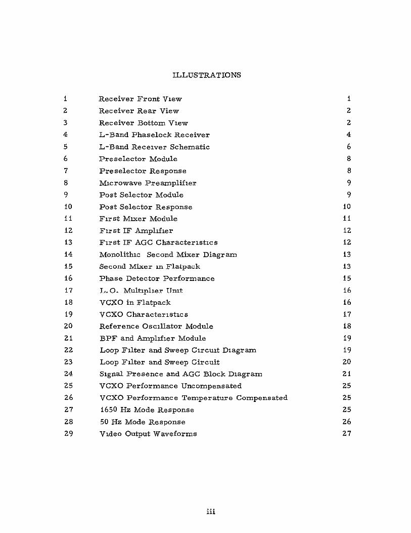

0
-2 1550 MHz
RECEIVER CENTER
-6
-8
-10
-12 0
-34
-16
-18 IMAGE FREQUENCY -i
-20 I
-22 I
-24
144 148 1$2 156 160 164 168 REQUENCY (GHz)
Figure tO Post Selector Response
34 FIRST MIXER
This balanced microwave mixer is built on a sapphire substrate
(Figure II) and has the following characteristics
Center frequency- i 6 gHz
Bandwidth too MHz
IF frequency 60 4 MHz
Noise figure lt9 dB
35 FIRST IF AMPLIFIER
The 62-MHz first IF amplifier has 70 dB of gain and 40 dB of AGC
The large allocation of gain for this circuit is intentional to keep the gain
in the 268 MHz second IF amplifier down to 30 dB The gain of the
second IF stages is kept low so that the receiver will not lock onto itself
The first IFcircuit consists of three Philco PA 7600 broadband monoshy
lithic amplifiers and a two-pole bandpass filter inserted between the second
10
Figure it First Mixer Module
and third stages The filter bandwidth is 6 MHz AGC for the first IF is implemented by the combination of a pin diode connected as a variable attenuator between the first and second stages plus controlling the gain of all three stages simultaneously
Figure 1Z is a photograph of the amplifier and Figure 13 illustrates the AGC characteristics
36 SECOND MIXER AND SECOND IF AMPLIFIER
The second mixer and second IF amplifier are combined in one module In the second mixer portion the 62-MHz information signal is converted to 26 866666 M1-z by proper interaction with the 88 866666 MHz reference oscillator Figures 14 and 15 show the circuit diagram and the photograph of the second mixer The mixer is a monolithic circuit that is manufactured by TRW and consists of a two-transistor device with the first transistor being the mixer and the second transistor being the impedshyance matching emitter follower stage The 62-M-z signal is applied to the base of the first transistor while the 88 86 1MHz reference oscillator
it
Figure 12 First IF Amplifier
8I
60shy
5O
g
40
20
lo0 02 04 06 08 10 12 14
AGC IV)
Figure 13 First IF AGC Characteristics
12
0
bull ----- 0( +2V
SIGNAL INPUT (Do -- F_ copyIFOUTPUT
8886 MHz REFERENCE OSCILLATOR
Figure 14 Monolithic Second Mixer Diagram
0Figure 15 Second Mixer in Flatpack
13
signal is injected into the emitter A resistor-capacitor low-pass
network is inserted between the two transistors to attenuate the local
oscillator leakage signal
37 PHASE DETECTOR AND VIDEO AMPLIFIER (DATA CHANNEL)
The receiver uses three identical phase detectors one for the data
channel the second for the loop filter and the third for the coherent
amplitude detector (CAD) of the signal presence circuitry All of these
three-phase detectors are monolithic (Type MC i596G manufactured by
Motorola) The circuit consists of an input differential amplifier driving
a pair of synchronized single-pole double-throw switches The switches
use transistor current mode gates with collectors cross-coupled in such
a manner that a full-wave balanced multiplication results between an
input voltage and the reference switching voltage
Figure 16 shows the output scale factor at 268 MHz in millivolt
radians versus reference signal levels for input signals of -10 to -30 dBw
The data channel phase detector is followed by a monolithic video
amplifier (Type CA30ZSA manufactured by RCA) This circuit is a lowshy
power differential amplifier that converts the differential output of the
phase detector into a single-ended output The frequency response of
this module has been adjusted for a 3-MHz bandwidth into a 1000-ohm load
A complementary follower or other video power stage will be necessary
if the receiver is to drive a 50-ohm line
38 LOCAL OSCILLATOR MULTIPLIER
The local oscillator (L 0) multiplier chain receives its 26 866-MHz
input signal from the voltage-controlled crystal oscillator (VCXO) and
multiplies it by a factor of 60 The i 612-gHz output signal is then fed
to the first mixer as the L 0 signal The L 0 multiplier chain conshy
sists of three transistorized multipliers with multiplication factors of
6 5 and 2
Each transistorized multiplier consists of two stages the first one
operated in Class A mode and the second one in Class B or C Each
multiplier is followed by a filter to eliminate the spurious responses
14
SIGNAL -10 din 900
800
700 SIGNAL -20 d~n
500
n400 0
SIGNAL -3Bdm
200
-30 -20 -10 0
REFERENCE SIGNAL (dim)
Figure 16 Phase Detector Performance
The entire circuit is made with discrete components with the exception of
the XZ filter which is a combline filter built on a sapphire substrate
employing microminiature technology The input and output impedance
of each multiplier is approximately equal to 50 ohms therefore each
unit may be aligned and tested independently A photograph of the entire
L 0 multiplier unit is shown in Figure iM
39 VCXO AND BUFFER
The oscillator circuit is a Colpitt type with emitter feedback A
varicap is used as the voltage-tuned frequency-determining element
The circuitry of the VCXO is a hybrid type packaged in a 38 x 38 flatpack
(Figure 18) The measured VCXO characteristics are shown in Figure 19
Because of the X60 multiplier the frequency variation required of the
VCXO is only 420 Hz from its center frequency of 26 866666 MHz An
emitter follower follows the VCXO to supply four output signals of
- i dBn each for the various circuits of the receiver The stability of the VCXO is better than 5 ppm within the temperature range of 100C to
400 C and the frequency range of interest
i5
Figure 17 L 0 Multiplier Unit
-V
Figure 18 VCXO in Flatpack
16
ROOM TEMPERATURE
+8
0+7 0 gt
gt aCN TER
FREQUENCY
+5
200 400 600 800 200
26866000 26867000
OUTPUT FREQUENCY (MHz)
Figure 19 VCXO Characteristics
3 iO REFERENCE OSCILLATOR
The reference oscillator (XO) is also a Colpitt type The same
masks used in the manufacturing of the VCXO were used for the XO The
difference between the VCXO and the XO is in the tuning elements and
crystal frequency The XO generates an 88 866666-Mqz signal with an
output power of -5 dBm and the stability is t10 ppm within the specified
temperature range The stability of the reference oscillator is masked
by the multiplier factor of the L 0 multiplier chain Figure Z0 shows
the reference oscillator module
3 ii BANDPASS FILTER AND AMPLIFIER
At threshold input the SIN ratio at the second IF amplifier is -30 dB
To improve this condition and to avoid noise saturation of the phase detecshy
tors for the loop filter and AGC circuitry a bandpass filter (BPF) is
placed in the signal path The bandwidth of the BPF is 500 kHz resulting
in an improvement of the SN ratio of 10 dB
17
i4 Figure 20 Reference Oscillator Module
The BPF is a three-pole filter centered at 26866 MHz and followed by a two-stage IC amplifier to compensate for the losses in the filter Figure 21 shows the BPF and amplifier module
3 12 LOOP FILTER AND SWEEP CIRCUIT
A block diagram of the loop filter and sweep circuit module is shown in Figure 2Z The inputs to this module are the 2686 MHz IF signal from the bandpass filter module and the 2686 MHz VCXO signal The output of the phase detector is then filtered in the active loop filter and fed to the VCXO closing the loop when coherency appears
The loop noise bandwidths (ZBL) are determined by the time conshystants associated with the active loop filter Bandwidth switching is accomplished by changing the time constants with miniature relays The relays are operated by the signal presence module
Prior to acquisition the VCXO is swept with a sawtooth waveform of 0 38 sec duration applied to the VCXO drive control voltage The sawshytooth waveform is generated in the active loop filter acting as an integrashy
18
Figure Zi BPF and Amplifier Module
PHASE DETECTOR
ACTIVE LOOP FILTER
K2
__
C
IF SGNALTO VCXO DRIVE
CURRENTLEVL
K4 f K3VCXO
MANUAL ACQUISITION
MONITOR
SOURCE
AMPLIFIER
DTCO
NO
Figure 22 Loop Filter and Sweep Circuit Diagram
i9
tor The current source amplifier supplies either positive or negative
current to the input of this integrator through resistor R The period of
oscillation is determined mainly by the product of R and C
The level detectors Nos I and Z sense the upper and lower levels
of the sawtooth waveform and supply this information to the current source
amplifier through the R-S flip-flop Once either of the two levels has been
reached the flip-flop reverses the jntegrating current A photographof the
loop filter and sweep circuit is shown in Figure 23
313 SIGNAL PRESENCE AND AGC AMPLIFIER
The signal presence and AGC amplifier module performs the followshy
ing tasks
Drives the signal presence light to indicate when the receiver has acquired and locked onto an incoming signal
Supplies a digital signal to the bandswitching relays to change bandwidth from 1650 Hz to 50 Hz when coherence is attained
64O1 69
Figure 23 Loop Filter and Sweep Circuit
20
0 Supplies a coherent AGC voltage to control the gain of the first IF amplifier
Drives the signal strength meter to indicate input level at the receiver
The input signals to this module are the 2686 MHz IF signal and
the 2686 MHz VCXO signal The circuitry consists of a phase detector
connected as a coherent amplitude detector (CAD) followed by a threshold
level detector (pA710) and digital drivers (SGi3Z) for the signal presence
light and bandswitching relays
The CAD also drives the AGC amplifier (LH201 No 2) The gain
of the AGC amplifier is set to cause only a 3-dB change in the second IF
output when the input signal to the receiver varies from -i30 dBm to
-90 dBm Because of scale factor and polarity a separate amplifier
drives the signal strength meter A block diagram of the signal presence
and AGC circuitry is shown in Figure 24
CAD THRESHOLD DETECTORI I
SIGNAL
SIGNALA
TO ELAYS
AGC AMPLIFIER
SIGNAL STRENGTH
- TO FIRST IF
Figure 24 Signal Presence and AGC Block Diagram
21
314 POWER SUPPLY
The supply voltages required to operate the receiver are + 12 -12
+ 6 and -6 V Regulated power supplies are necessary to be able to
track the negative output with the positive output since several operational
amplifiers are used throughout the receiver A dynage module (K iZiZshy
0 5010 50 AKR) dual output dc power supply was selected for the 12 V
with the following specifications
Input 105-125 Vac 50 to 400 Hz
Output 12 V at 05 A each
Regulation combined 005
Ripple 2 mY rms
Tracking t0 005degC
Temperature coefficient 003degC over range
-20degC to + 600C
Temperature operating -20degC to + 7idegC
The +6 and -6 V power supplies are derived from the 12 V supply
in a separate regulator card The 6-V regulator consists of a temperatureshy
compensated zener and an operational amplifier followed by a passing
transistor
22
4 RECEIVER TEST RESULTS
AUI the receiver parameters called out in Table I have been tested
according to the test procedure described in Appendix A Table II shows
those parameters with their respective design goals and the measured
values
TABLE II
RECEIVER TEST PARAMETERS
Test No Parameter
I Carrier frequency
2 Carrier acquisition threshold
3 Carrier acquisition level
4 Carrier tracking level
5 Signal dynamic range
6 Receiver noise figure
7 IF bandwidth D channel 8 VCXO stability
(i0 0 to 400 C)
9 VCXO sweep range
i0 Sweep period
I I Probability of lock at -127 dBm one sweep
12 Differential time delay
03 Receiver operational temperature range
14 Acquisition loop bandshywidth 2 BL
15 Tracking loop bandshywidth 2 BL
Measured Design Goal Values
1550 gHz 25
-130 dBm
-125 dBm
-134 dBm
40 dB
6 dB
5 Ml-z
i0 ppm
416 Hz
0 38 sec
0999
15 msec
10C to 400 C
kHz 1550 gHz 25 kHz
-131 dBm
-125 dBrm
-135 dBm
40 dB
52 dB
5 MHz
22 ppm
420 Hz
038 sec -002 sec
Not directly measured 9 nsec
10 C to 400 C
1650 Hz Approx 1780 Hz
50 Hz Approx 5i Hz
Z3
During the nionth allocated for testing and integration with the
BINOR processor it became evident that the following corrections were necessary
a AGC characteristics
b Temperature compensation of the VCXO
c Lower the output impedance of the video output
Items a and b were corrected but Item c was not considered urgent provided the cable connecting the video output of the receiver
to the BINOR processor was kept short
The following paragraphs clarify the test results for the signal dynamic range VCXO and loop bandwidth measurements
4 1 SIGNAL DYNAMIC RANGE
The receiver has an input dynamic range of 40 dB The gain of the
AGC amplifier was adjusted to maintain the signal output from the second
IF amplifier within 3 dB
42 VCXO STABILITY
The VCXO stability required is 10 ppm over the temperature range of 1oo to 40CC The uncompensated VCXO shows stabilities of 14 ppm and is illustrated in Figure 25
Thermistor-resistance stabilization was used resulting in Z 2 ppm over the temperature and frequency ranges Figure 26 illustrates the
compensated VCXO
43 LOOP BANDWIDTH
The loop bandwidth of the receiver was measured with an input
signal of -124 dBm as described in the test procedure in Appendix A Figure 7 shows the response for the 1650-Hz mode and Figure Z8
depicts the response for the 50-Hz mode
24
-6 +9
+5 +8
0 +4 gt 7
gt r
+3 +6 r-CENTER FREQUENCY CENTER FREQUENCY 26866666 MHz
26866666 MHz
4-2 I 00 +5
S=+40C
4III
26866000 26867000 26866000 268670M0 FREQUENCY (MHz) FREQUENCY (MHz)
Figure 25 VCXO Performance Figure 26 VCXO Performance Uncompensated Temperature
Compensated
1650 Mx MODE
- 124 db INPUT
-4shy
-
-6 1
10 Hz
1 1 1 1 1 1 1 1
100 Hz
I i i i I I
1000 Hz
Figure 27 1650 Hz Mode Response
25
2 -
1
0
50 Hz BANDWIDTH -124 d~m INPUT
-I
-2
-3
-4
-5
-6
-7 1 I Hz
1 1 1 1 10 Hz
I i1 1000 Hz
Figure Z8 50 Hz Mode Response
26
5 BINOR TEST RESULTS
The interface preliminary tests consisted of the L-band transmitter
modulation with the BINOR code or the 3 iZ kHz top tone transmission to
the receiver and processing of the receiver output
After the receiver AGC was adjusted the signal level into the
BINOR processor stayed within the acceptable limits for a wide range of receiver input levels The receiver output coupling capacitor needed to be increased because of an inadequate correlation level on the lowest subshy
frequency tone to the code processor
The receiver-to-processor interface also required close proximity of the two units because of the high output impedance of the receiver and may require receiver changes for impedance matching Printout of the processor output indicated that the system concept and method is practical
and feasible
Figure 29 illustrates the output of the receiver with three different
signal input levels In comparison to the upper two waveforms the sigshy
nal in the bottom portion of the photograph was completely buried within
the noise when adjusted for a minimum signal level but lock-in and proshycessing by the BINOR code processor were easily accomplished with no
errors
Figure 29 Video Output Waveforms
27
APPENDDC A
The test procedure for the L-band phase-lock
receiver is included in this appendix This procedure
explains the tests performed for the fifteen parameters
called out in the receiver specifications The block
diagram test setup the test equipment required and
the test procedure are given for each parameter
A-I
TEST PROCEDURE FOR THE L-BAND PHASE LOCK RECEIVER
Documentation required 1) Schematic L-Band Receiver SK68137
2) L-Band Phaselock Receiver Modules Interconnections SK68138
10 Carrier Frequency Figure A-1 shows one of the suggested RF source
configurations to test most of the receiver parameters
set-up
8614A HP
g Ge
1550 MHz L-Band
Phase Modulator
120 db P
at
arable3MHI
Atten
T
R
HP
Fre uency
I Synthesizer
F
IF Re
2650 P
Oscillator
Synthesizer
EH 122
Pulse Gen
Binor Gen
(or
Figure A- I
V
A-Z
11 Test Equipment Required Frequency Synthesizer HP 51008 Oscillator Synchronizer HP 2650A o Signal Generator HP 8014A o Pulse Generator EH 122 o Binor Code Generator (TRW) L-Band Phase Modulator (TRW) Calibrated Variable Attenuator HP 394A
12 Test Procedure
o Measure the frequency of the 8614A Signal Generator with
5245-L Electronic Counter Hp or equivalent
Make necessary adjustment to the IF reference frequency so
as to read a frequency of 1550 NHz from the Signal Generator o Record frequency reading on test data sheet
20 CARRIER ACQUISITION THRESHOLD 21 Test Equipment Required
RF Test source of Figure A-1 o Power meter HP 431C
22 Test Procedure o Measure RF power available at the input of the receiver with
431C Power Meter HP Add sufficient attenuation following the signal generator soO
as to decrease the available power at the output of the coaxial
calibrated attenuator to -81 dbm when the dial is reading 6 db o Turn the Mode Selector switch of the receiver to-165050 Hz
mode and set the calibrated coaxial attenuator to -145 dbm
output
Increase the RF power to the receiver from -145 dbm until the
receiver shows signs of threshold locking o Record carrier acquisition threshold level on data sheet
30 CARRIER ACQUISITION LEVEL
31 Test Equipment Required o RF Test source of Figure A-1
A-3
32 Test Procedure o Increase the RF power to the receiver to -125 dbm Receiver
should remain locked
40 CARRIER TRACKING LEVEL
41 Test Equipment Required a RF Test source of Figure A-i
42 Test Procedure
o Decrease the RF power to the receiver from -125 dbm to -134 dbm
Receiver should continue in locked condition
50 SIGNAL DYNAMIC RANGE
51 Test Equipment Required
o RF Test source of Figure A-I o Spectrum analyzer HP 851B85518
52 Test Procedure
o Connect spectrum analyzer to the 2nd IFamplifier output pin 5
o Set the RF test source to feed -130 dbm signal to the input
of the receiver o Set the spectrum analyzer in a narrow IFbandwidth to
observe the carrier signal
Increase the input signal to the receiver by 40 db Output
signal observed in the spectrum analyzer should remain
constant within 4 db
60 RECEIVER NOISE FIGURE
61 Test Equipment Required o Noise figure meter
o UHF Noise Source
o 10 db Pad
62 Test Procedure
HP 342A
HP 349A
o Set up equipment as shown in Figure A-2 Notice that the UHF Noise Source has a 10 db pad following removal
of this pad will damape the receiver Pre-amplifier
A-4
62 Test Procedure (continued)
o Adjust the zero and infinity adjustments of the noise figure meter
before taking a reading Noise figure should read between 5 to 6 db Record measurement on data sheet
r _ Noise Figure Meter f UHF Noise 10 db Receiver
I Source Pad Under Test
enHP-3A 349A HP I__--
I Is IFI_) _n_____---
IL
Figure A-2
A-5
3
2
50 Hz BANDWIDTH -124 dm INPUT
0
-1
-2
-3
-4
-5
-6
-7 L I I II
1 Ha 10 Hz 1000 H
Figure 28 50 Hz Mode Response
Z6
5 BINOR TEST RESULTS
The interface preliminary tests consisted of the L-band transmitter modulation with the BINOR code or the 3 iZ kHz top tone transmission to the receiver and processing of the receiver output
After the receiver AGC was adjusted the signal level into the BINOR processor stayed within the acceptable limits for a wide range of receiver input levels The receiver output coupling capacitor needed to be increased because of an inadequate correlation level on the lowest subshyfrequency tone to the code processor
The receiver-to-processor interface also required close proximity of the two units because of the high output impedance of the receiver and may require receiver changes for impedance matching Printout of the processor output indicated that the system concept and method is practical and feasible
Figure 29 illustrates the output of the receiver with three different signal input levels In comparison to the upper two waveforms the sigshynal in the bottom portion of the photograph was completely buried within the noise when adjusted for a minimum signal level but lock-in and proshycessing by the BINOR code processor were easily accomplished with no errors
Figure 29 Video Output Waveforms
Z7
APPENDIX A
The test procedure for the L-band phase-lock
receiver is included in this appendix This procedurq
explains the tests performed for the fifteen parameters
called out in the receiver specifications The block
diagram test setup the test equipment required and
the test procedure are given for each parameter
A-1
TEST PROCEDURE FOR THE L-BAND PHASE LOCK RECEIVER
Documentation required 1) Schematic L-Band Receiver SK68137
2) L-Band Phaselock Receiver Modules Interconnections SK68138
10 Carrier Frequency Figure A-i shows one of the suggested RF source set-up
configurations to test most of the receiver parameters
20 db 8614A HP 1550 MHz L-Band Pad I r9AeHl TO Sig Gen Phase Hl2 AttenW R
Modulator-A
S5100B HP R-2650A HP EH 122
Frequency IF Ref Oscillator Pulse Gen (orI Synthesizer _rSynthesizer Binor Gen
Figure A-1
A-2
11 Test Equipment Required o Frequency Synthesizer HP 5100B
o Oscillator Synchronizer HP 2650A o Signal Generator HP 8014A
o Pulse Generator EH 122 o Binor Code Generator (TRW)
o L-Band Phase Modulator (TRW)
o Calibrated Variable Attenuator HP 394A
12 Test Procedure o Measure the frequency of the 8614A Signal Generator with
5245-L Electronic Counter Hp or equivalent o Make necessary adjustment to the IFreference frequency so
as to read a frequency of 1550 MHz from the Signal Generator o Record frequency reading on test data sheet
20 CARRIER ACQUISITION THRESHOLD
21 Test Equipment Required o RF Test source of Figure A-I o Power meter HP 431C
22 Test Procedure Measure RF power available at the input of the receiver with
431C Power Meter HP o Add sufficient attenuation following the signal generator so
as to decrease the available power at the output of the coaxial calibrated attenuator to -81 dbm when the dial is reading 6 db
o Turn the Mode Selector switch of the receiver to-165050 Hz mode and set the calibrated coaxial attenuator to -145 dbm output
o Increase the RF power to the receiver from -145 dbm until the
receiver shows signs of threshold locking o Record carrier acquisition threshold level on data sheet
30 CARRIER ACQUISITION LEVEL
31 Test Equipment Required o RF Test source of Figure A-I
A-3
32 Test Procedure o Increase the RF power to the receiver to -125 dbm Receiver
should remain locked
40 CARRIER TRACKING LEVEL
41 Test Equipment Required o RF Test source of Figure A-i
42 Test Procedure
o Decrease the RF power to the receiver from -125 dbm to -134 dbm
Receiver should continue inlocked condition
50 SIGNAL DYNAMIC RANGE
51 Test Equipment Required o RF Test source of Figure A-i O Spectrum analyzer HP 851B8551B
52 Test Procedure Connect spectrum analyzer to the 2nd IFamplifier output pin 5
o Set the RF test source to feed -130 dbm signal to the input
of the receiver o Set the spectrum analyzer ina narrow IFbandwidth to
observe the carrier signal o Increase the input signal to the receiver by 40 db Output
signal observed in the spectrum analyzer should remain constant within 4 db
60 RECEIVER NOISE FIGURE
61 Test Equipment Required o Noise figure meter HP 342A
o UHF Noise Source HP 349A
o 10 db Pad
62 Test Procedure o Set up equipment as shown in Figure A-2
Notice that the UHF Noise Source has a 10 db pad following removal
of this pad will damage the receiver Pre-amplifier
A-4
62 Test Procedure (continued)
Adjust the zero and infinity adjustments of the noise figure meter
before taking a reading Noise figure should read between
5 to 6 db Record measurement on data sheet
Noise Figure Meter UHF Noise 10 db V Receiver HP 342A i Source Pad Under Test
349A HP
60 MHz Ist IF 1
Figure A-2
A-5
70 IF BANDWIDTH DATA CHANNEL
71 Test Equipment Required o Power Meter HP 431C
o Signal Generator HP 606C
72 Test Procedure O Reconnect the equipment as shown in Figure A-3 o Sweep manually the input frequency to the Ist IF and record
upper and lower frequencies resulting in 3 db drop from
the 62 MHz center frequency o The difference between the two readings is the bandwidth
of the IF data channel Record the bandwidth on data sheet
st IF 2nd Mixer amp Meter
Amplifier HP 431C
Signa88-866 Ref Osc
Generator 8 HP 606C
Figure A-3
A-6
80 VCXO STABILITY (100 to 40degC)
Data onthis test is available in Engineering Notebook No 8904
Examination of this data can be used to determine the VCXO stability
inlieu of an actual test
81 Test Equipment Required O Test oven
o Frequency counter HP5245L
o Precision power supply EPCO model
82 Test Procedures o Connect equipment as shown in Figure A-4
OVEN
I co IVCXO Frequency 12V Under Counter
Test -
I - - Cwnt~or Voltage
IPrecision PS
Figure A-4
o Vary the temperature of the oven from OdegC to 500C in 10 degree
intervals 0 For each temperature setting vary the control voltage from
+1 to +7 in steps of I volt o Record and tabulate the data
A-7
90 VCXO SWEEP RANGE The receiver has been designed with a sweep range of + 25 kHz The VCXO preceeds a times 60 multiplier chain therefore the actual deviation of the VCXO is 160 of + 25 kHz or + 416 Hz From the data taken inparagraph 8 the scaling factor (approximately
416 Hzvolts) can be obtained The amplitude of the sawtooth waveform sweeping the VCXO determines the sweep range
91 Test Equipment Required o Osci-loscope Tektronix 585
92 Test Procedure o Connect oscilloscope to test point marked TP on the
Loop Filter and Sweep Circuit module o Measure peak-to-peak amplitude of the sawtooth waveform o Calculate and record the sweep range
100 SWEEP PERIOD
101 Test Equipment Required o Oscilloscope Tektronix 585
102 Test Procedure o Connect oscilloscope to test point TP of the loop filter and
sweep circuit o Measure and record the sweep period
110 PROBABILITY OF LOCK (-127 dbm) on one sweep A direct measurement of probability of lock requires several thousands locking operations and a correlation of the compiled data into a single
number
Probability of lock of 0999 becomes very difficult to measure and beyond the scope and capabilities of this program therefore this
test cannot be performed at this time
It is important to notice that the probability of acquisition is a function of several parameters such as signal to noise ratio threshold
sensitivity dampinq factor sweep rate loop bandwidth etc
A-8
It has been demonstrated ()that the smaller the ratio of sweep rate
and loop noise bandwidth the greater is the probability of lock for
a given signal to noise ratio and damping factor
The ratio just mentioned is 0046 for this receiver and it is
obtained as follows
ratio = R = 25xi0 302 = 0046 (1650)2(Bno)2
Figure 3 of the referenced paper shows that the probability of lock
for a 10 db SN and damping factor of 07 is 95 when this ratio
is 012 Therefore the 0046 ratio is an assurance that the
probability of lock is better than 95
120 DIFFERENTIAL TIME DELAY
121 Test Equipment Required o AD-YU 202 Vectorlyzer
o Binor Code Generator
o Binor Processor
122 Test Procedure
o Connect the system as shown in Figure A-5
JP Frazier and J Page Phase Lock Acquisition Study
IRE Trans on Space Electronics and Telemetry page 211
figure 3 September 1962
A-9
Binor CodeGenerator II
600 Binor ohms
code
AD-YU 202 Vectorlyzer
E2 El
Binor I
Processorr_- - -Li0sc
IHFDiv Card LI
Car
H
R-F ~~20db Rcie
Source -
L-Band Phase
Modulator___ Pad - -
Variable Attenuator
Receiver Under TestL _Video
Figure A-5
122 Test Procedure (Continued)
0 Set the Binor Code Generator switches as follows
Mode Switch to CW
Clock Switch to RUN
OUT Switch to NORM
OscSel Switch to INT
Gate Switch to INT
AC Power Switch to ON
deg Adjust the Vectorlyzer per manufacturer procedure on the 0-180 deg scale
bull LFIP supplies a 300 kHz signal from the binor processor oscillator which
is phase locked to the fundamental of the video output of the receiver
providing a noise-free signal for use in the differential time delay A
measurement
A-10
122 Test Procedure (Continued) o Set the RF attenuator for -121 dbm signal to the input of the
receiver and note the phase difference o Increase signal to the receiver to -81 dbm Note the maximum
phase deviation from step above
Multiply maximum phase deviation observed in step above by 925 nsec
per degree The resulting value isthe absolute value of differential
time delay
O
130 RECEIVER OPERATING TEMPERATURE RANGE TEST
131 Test Equipment Required deg Test oven for 100C to 400
o Frequency source set-up as per Figure A-I
132 Test Procedure Place receiver inthe oven and set temperature to 10C After
20 minutes at that temperature check carrier acquisition threshold
O
o Repeat above step for temperature of 20 30 and 400C
deg All the preceeding tests should show a -130 dbm carrier acquisition
threshold or better Record test in data sheet
140 ACQUISITION LOOP BANDWIDTH (2BLs 1650 Hz)
141 Test Equipment Required O Signal Generator HP 8614A
O Oscillator Syncronizer HP 2650A
o Frequency Synthesizer HP 5100B 0 Synthesizer Driver HP 5110B
Dual DC Power Supply HPHarrison 6205B
0 Pin Diode Switch Modulator
Waveteck III Voltage Controlled Generator
o DC Power Supply HP 721A
o Oscilloscope Tektronix 453
Variable Attenuator HP 394A
O 20 db Pad
0
O Wave Analyzer HP 302A
o AC Transistor Voltmeter HP 403A
o Oscilloscope Tektronix 585
A-11
141 Test Equipment Required (Continued) Transmitter Assembly Test Set-up o Connect the transmitter assembly as shown in Figure A-6 o Set the following switches to the indicated position
Tektronix 453 Oscilloscope
Power switch to ON Vertical 2 Vcm DC
o Waveteck III VC Generator
Power switch to Xl
Output selector to Sine wave
o HP 721A Power Supply
Power switch to ON
Voltage adjust pot to -55 VDC (seen on the 453 oscilloscope) o Harrison 6205B Dual Power Supply
Power switch to ON (Modulator power switch should be OFF)
Both Voltage pots to 20 volts DC Wiring should be set up to provide both +20V and -20 volts to the modulator
o Modulator
Power switch to ON
o HP 8614 Signal Generator
Line switch to ON
RF switch to ON
ALC switch to ON Ext FM switch to ON
DBM meter to 0 Attenuation dial to -045 db Frequency dial to 1554 MHz
o HP 5100B HP 5110B Synthesizer
Power switch to operate (both 5100B and 5110B)
Frequency standard switch to INT Frequency selection switch to Local Keyboard Frequency Keyboard switch to 3001005000 Hz Search control switch to Remote
A-12
INSIDE SCREEN ROOMOUTSIDE SCREEN ROOM
HPHarrlson + Modulator 0 Variable ttn Output
6205 B Dua Pwr Sup 20V
0db Port 3PadTo
inpU Attenuator
HP 394A
to Output Receiver
-Video I n shy -
Calib
RF Out
HP 8614A Signal Gen
xt FM Uncal
5 Inc_ - - -
SIF tReAflnu
Y ntsc Tektronix 453
HP 2650 Oscilloscope
Output HP 5100B
Wavetek III VC Gen
SynthesizerAssembly Search --
J output
NOTE Use caution with the
Control Control___ -
ground wiring This generator is operated at an elecated DC level
HP 721A Power Supply
Figure A-6
141 Test Equipment Required (Continued)
o HP 2650A Synchronizer
Power switch to ON
IF Mode switch to EXT
APC switch to ON
Search light should be OFF
Phase meter should be slightly off center This is
accomplished by adjusting the HP 8614A signal generator
frequency
o HP 394A Variable Attenuator
Set the variable attenuator control dial to read 49 db of attenuation (This provides a power into the receiver
of -124dbm)
Allow a 30 minute warm up period before conducting test
Receiver Test Set-up o Connect the receiver assembly as shown in Figure A-7 o Set the following switches to the indicated positions
o HP 403A AC Transistorized Voltmeter
Range switch to 0 db ( 1V RMS full scale)
Function switch to 1 cps - 1 Mc
o Tektronix 585 Oscilloscope
Power switch to ON
Vertical to 1 Vcm DC
o HP 302A Wave Analyzer
Power switch to ON
Scale Value switch to Absolute
Mode selector switch to Normal
o L-Band Phase Lock Receiver (Unit under Test)
Power switch to ON
Allow a 30 minute warm-up period before conducting tests
142 Test Procedure 1650 Hz Noise bandwidth
o The HP 302A Wave Analyzer should be connected to point reg in figure 7 The Mode Selector switch on the receiver should be
in the 1650 Hz AUTO position Set the frequency of the Wavetek Ill oscillator to 250 Hz
A-14
Transmitter Assembly Output from Variable Attenuator
L-Band Phaselock Receiver
Loop Filter and Sweep Circuit
PinLH[OI6 TPI
1
IInput
HP 302A Wave Analyzer
Output
4 input
HP 403A AC Trans-istorized Voltmeter
4 vent-in
Tektronic 585 Oscilloscope
Ficure A-7
Vary the ATTEN control on the Waveteklll oscillator and the
FREQ Keyboard setting of the HP 5100B FREQ Synthesizer until
a reading of -40 db is observed on the HP 302A wave analyzer meter (The Frequency control on the Wave Analyzer will need to be adjusted
for a peak at 250 Hz and the MODE Selector set to AFC) The
proper setting of the FREQ Keyboard will be one of the following
settings 3 0 0 1 0 0 0 50 0 Hz
3 0 0 1 0 0 5 00 0 Hz
3 0 0 1 0 5 0 00 0 Hz
3 0 0 1 5 0 0 00 0 Hz
O Note the signal level in db for various frequencies ranging
from 10 Hz to 2 kHz The procedure for this isto set
the frequency of the Wavetek 111 oscillator to the desired
setting Set the MODE selector on the wave analyzer to NORMAL Adjust the Wave Analyzer Frequency control until a peak
isobserved then replace the MODE Selector to AFC Read the signal
indb directly from the Wave Analyzer meter Compare this data
with figure 3-3 inreference No 1 in order to determine the
damping factor and the loop resonate-frequency
150 TRACKING LOOP BANDWIDTH (2BL) 50 Hz)
151 Test Equipment Required o Same as paragraph 141
Transmitter Assembly Test Set Up 0 Same as paragraph 141
Receiver Test Set Up o Same as Paragraph 141
152 Test Procedures 50 Hz Noise Bandwidth 0 The HP 302A wave analyzer should be connected to point Q
infigure 7 The mode selector switch on the receiver should be inthe 165050 Hz AUTO position Set the frequency of the Wavetek Ill oscillator to 10 Hz
A-16
152 Test Procedures 50 Hz Noise Bandwidth (Continued) 0 Using the procedure of paragraph 142 second item obtain a meter
reading of -10 db at a frequency of 10 Hz Adjust the OUTPUT AMP
pot on the Wave Analyzer until the HP 403A AC transistorized
voltmeter reads 0 db Note The range of this meter is now identical to the range of the
Wave Analyzer This setup may be used down to the frequency
of 3 Hz It should not be used below 3 Hz and at this frequency 1 db should be added to the meter reading At 4 Hz and above
the meter may be read directly o Using the procedure of paragraph 142 third item obtain the signal
level for various frequencies ranging from 3 to 30 Hz The signal should be read in db from the HP 403A voltmeter The
Tektronix 585 scope is provided to aid in the peaking of the signal Compare this data with figure 5-1 in reference No 1
in order to determine the loop resonate frequency o The HP 302A Wave Analyzer should be connected to point reg
in figure 7 The Mode Selector switch on the receiver should be
in the 165050 Hz AUTO position Set the frequency of the Wavetek Ill oscillator to 10 Hz
o Using the procedure of oaragraph 142 second item obtain a
meter reading of -70 db at a frequency of 10 Hz Usini the procedure of paragraph 152 second item calibrate the HP 403A Voltmeter
o Using the procedure of paragraph 142 and 152 third items obtain
the signal level for various frequencies ranging from 3 Hz to 100 Hz Compare this data with figure 3-3 of reference No I to obtain the damping factor
Reference No 1 Theory of Phaselock Techniques as applied to Aerospace
Transponders Floyd M Garner and Steven S Kent
Contract No NAS8-11509 Marshall Space Flight Center
NASA Huntsville Alabama
A-17
APPENDIX B
The modules interconnections diagram is
included to serve as an aid in receiver maintenance
All cabling is coaxial with the exception of the
color-coded power supply wiring meters and
selector switches
B-1
_ 7 643 2
CK PANEL) VIDEO OUTPUT
PRESELECTOR PRE-AMP POST IT IF 2ND MIXER s VIDEO AND SLCF
VIDEOOUPUM (BACKPANEL)
IN INIIGNNAG
STRENGTH MS3IO2ELIOSL-3P P
(FRONT PANEL
N(FON) OFF SWITCH (FRONT)N MLTIPIERMULIPIE -V-12V -GD PAAINALP(FPANEAMD-PL PRESENCE
FUSE HOLDER (BACK) + 3- CAD TEST C
POWER SUPPLY
1212 050050IG REL
L - VCXO AI
+12V LOOP FILTER AND - I aV G O -2 SWE EP C T
R3
-6D VCXCMONITOR -J-I
-6 -6 -12 -12I
MNUAL ACQUISITION CFRONT PANEL) regMODE SELECTOR
(FRONT PANEL) B
4M2v
WIRING OQORCOD
REGULATOR CARD ING RED ___________
-22V BLUE
4 6 ORANGE _ _
A -6VI PURFLEI --__
GND BLACK L BAND PHASELOC
O 1650 MAN shy16 50 HI AUTO-165050 AUTO RCEINTER N
-I-ULES INTERCONNECTIONS
NOTESUNLESSOTHERWSS SPECIFWM
ri I I 5 ~ h~T
APPENDIX C
ALIGNMENT
REQUIRED TEST EQUIPMENT
The following test equipment
for performing these tests
Sweep Generator
CW Generator
Oscilloscope
Attenuator
Spectrum Analyzer
Power Meter
RF Detector-
Synchronizer
Synthesizer
Modulator
Power Supply
Loads
DC Milliamp Meter
Pulse Generator
PROCEDURE
AND TYPICAL TEST SET UP
or its equivalent should be on hand
Jerrold model 900C HP 8690A with 8691A plug-in
HP 606 50 kHz to 65 MHz HP 608 10 MHz to 480 MHz HP 642 450 MHz to 1230 MHz HP 8614A 800 MHz to 2400 MHz
Tektronix 453 Tektronix 585 with (CA type plug-in)
OSM model 20510-3 (3 db) fixed OSM model 20510-6 (6 db) fixed OSM model 20510-10 (40 db) fixed HP 394A (6-140 db) variable HP 8491A - 20 db (20 db) fixed HP 8491A - 10 db (10 db) fixed
HP 851B8551B
HP 431C with 478A thermistor
HP 423A
HP 2650A with 105 3333 MHz crystal
HP 510OB5110B
TRW Bi phase
HPHarr-ison 6205B (dual) (3 each) EPSCO VRS 611 HP 7Z1A
50 ohm OSM 20140P (4 each)
Simpson model 269
EH 122 TRW Binor code generator
C-I
Voltage Controlled Generator- Wavetek model 111
Frequency Counter HP 5245L with 5253 andS54 plug-in
Voltmeter HP 3430A
Noise Figure Meter HP 342A with the HP 349A UHF Noise Source
AC Voltmeter HP 403A (no equivalent)
Wave Analyzer HP 302A (no equivalent)
OUTSIDESCREEN INSIDE SCREEN ROOM
R-- 12V MODULATOR RSNI INTUTF MIABLE ATTNOUTPUT
DUA S P
HP TORECEIVER
Hp8614AISIGNALGENERATOR EXT FM UNCA
IPT RFO U
USECAUTION WITHTHE4535 GROUNDWRING mUSGENERATORIS OPERATED
C ATAN ELECATEDDC LEVEL
OUTPUTHP 510BKII SYNTHESIZER
ASSEMEampy
SEARCH
CONTROL
Figure 1 Transmitter Assembly Test Set-Up
The following test set-ups will be referenced frequently throughout
this procedure
1 1 RIF Test Set-Up
The R F Test Set-Up is illustrated in Figure 4 This set-up will
be used for the following modules
Pre-selector Pre-amplifier Post selector First IF amplifier Second mixer and second IF amplifier Narrowband filter L 0 multiplier
C-a
Each section of this test procedure will specify the connections used
(regthroughreg)or not used and the frequencies and power levels
associated with each connection From this the test equipment may be
easily selected from the provided list
In all sections of this test procedure the RF connections on the test
unit must be terminated into 50 ohms It is recommended that an
attenuator ( 3 to 10 db) or a 50 ohm load be placed on all connectors in
order to insure the proper load impedance and reduce cable effects
It is also recommended that all cables be kept as short as practical
It will be noted that when swept measurements are made then the
sweep generator the REF detector and the oscilloscope are used When
a GW measurement is made the CW generator is used in conjunction
with either the spectrum analyzer or the power meter Allow a 30
minute warm up before conducting tests
SIGNAL GNRIKOSCOPE
GENERATOR ENERATOR
DACPO
C-Figur 2NRUTetStU
SDC POWER
SUPPLIES
DC MILLIAMP
METER
EPSCOVRS 611
VCXODRIVE
UNITUNDER OUTPUT AEN SETUANALYZER
ADDITIONAL OUTPUTS POWER
Figure 3 Oscillator Test Set-Up
1 2- Oscillator Test Set-Up
The Oscillator Test set-up Is illustrated in Figure 3 This set-up
will be used for the following modules
Reference Oscillator VCXO and Buffer
Each section of this test procedure will specify the connections
used (regthrough) or not used and the frequencies and power levels
associated with each connection From this the test equipment may be
easily selected from the provided list
In all sections of this test procedure the RF connectors on the test
unit must be terminated into 50 ohms It is recommended that an
attenuator (3 to 10 db) or a 50 ohm load be placed on all connectors in
order to insure the proper load impedance and reduce cable effects It
is also recommended that all cables be kept as short as practical
Allow a 30 minute warm up before conducting tests
C-4
131
1 3 Transmitter Assembly Test Set-Up
Connect the transmitter assembly as shown in Figure 1
Set the following switches to the indicated position
Tektronix 453 Oscilloscope
Power switch to ON
Vertical Z Vcm DC
Waveteck III V C Generator
Power switch to Xi
Output selector to Sine wave
HP 721A Power Supply
Power switch to ON
Voltage adjust pot to -5 5 VDC (Seenon the 453 oscilloscope)
Harrison 620513 Dual Power Supply-
Power switch to ON (Modulator power switch should be OFF)
Both voltage pots to 20 volts DC Wiring
should be set up to provide both +Z0V and
-20V to the modulator
Modulator
Power switch to ON
HP 8614 Signal Generator
Line switch to ON
RF switch to ON
ALC switch to ON
Ext FM switch to ON
DB2A meter to 0
Attenuation dial to -045 dB
Frequency dial to 1554 MHz
tests only it will be called for inThis equipment is used for specific the procedure if required
C-5
HP 510GBHP 5110B Synthesizer
Power switch to operate (both 5100B and 5110B)
Frequency standard switch to INT
Frequency selection switch to Local Keyboard
Frequency Keyboard switch to 30010000 00 Hz
Search control switch to Local
Pulse Generator
Power Switch to ON
HP 2650A Synchronizer
Power switch to ON
IF Mode switch to EXT
APC switch to ON
Switch light should be OFF
Phase meter should be slightly off center This is accomplished by adjusting the HP 8614A signal generator frequency
HP 394A Variable Attenuator
Set the variable attenuator control dial to read 49 dB of attenuation (This provides a power into the receiver of -424 dBm)
Allow a 30 minute warm up period before conducting test
1 3 Z Transmitter Frequency Adjustment
Connect the counter to the output of the HP 8614A and adjust the
HP 5100B synthesizer frequency until the counter reads 4550 000 MHz
Reconnect the signal generator output to port I of the modulator
133 Power Calibration Procedure
Temporarily remove the 20 dB pad and set the variable attenuator to -10 dB
Connect the HP 431C power meter to point reg (Figure 1)
This equipment is used for specific tests only it will be called for in the procedure if required
c-6
Adjust the variable attenuator on the HP 8614 (oscillator) until -25 dBm is observed on the power meter
Replace the 20 dB pad and add 40 dB to the HP 8614 (oscillator) variable attenuator
The system is now calibrated so that the power input in -dBr to
the receiver is the sum of the HP 394A attenuator reading plus 75
2 SUBASSEMBLY ALIGNMENT PROCEDURES
Ten modules of the L-Band receiver require bench alignment
prior to receiver system test The remaining modules are tested and
aligned utilizing the receiver noise
2 1 Pre-Selector Test Procedure
Utilize the RF test set up of paragraph 1 1 and Figure 2
Connections Approximate requirements
reg input 1 55 GHz at -10 dBn
output 1 55 GHz at -10 dBm
copy (E) and ( un-used
This is a high pass filter It should have an insertion loss of less
than 4 dB and greater than 60 dB loss at 400 MHz The only adjustment
possible in this module is to replace the capacitors or change the length
of the inductors
2 Z Pre-Amplifier Test Procedure
Utilize the RF test set up of paragraph 4 1 and Figure 2
Connections Approximate requirements
reg input 4 55 GHz at -50 dBm
G output 4 55 GHz at -30 dBm
copy D and un-used
DC power +1Z 0 VDC at 10 ma
C-7
2
There is no provision for adjustment of this module It is a wideshy
band preamplifier with only the requirements that the gain at 1550 MHz
be greater than 15 dB that the 3 dB bandwidth be greater than Z0 MHz
(+ and -10 MHz) and that the noise figure be equal to or less than 5 dB
The gain and bandwidth may be tested on this set up however the
noise figure will be tested during the receiver front end alignment
(section 3 2)
CAUTION The preamp contains open circuitry and transistors Do
not touch the substrate or any part in this box
2 3 Post Selector Test Procedure
Utilize the RF test set up of paragraph I 1 and Figure Z
Connections Approximate requirements
G input 45 GHz at -40 dfm
output 1 55 GHz at -40 dBm
un-used
This is a bandpass filter that has an insertion loss of 2 dB or less
and a bandwidth greater than 20 MHz (+ and -40 MHz) at the 3 dB points
The image frequency range (1 665 to 4 675 GHz) must be greater than
20 dB down
The two capacitors should be adjusted with the unit set up in the
swept mode and the CW mode should be used to check the specifications
2 4 1st IF Amplifier Test Procedure
Utilize the RF Test set up of paragraph I I and Figure Z
Connections Approximate requirements
reg input 62 MHz at -80 dBm
output 62 MHz at -10 dBm
Sand reg un-used
AGC input 0 VDC (min gain) to 1 8 VDC (maximum)
DC input +6V at 55 ma
C-8
This high gain amplifier should have a gain of approximately 70 dB
at the center frequency of 62 MHz and a 3 dB bandwidth of 6 MHz (+3 and
-3 MHz) The AGC should have control over a dynamic range of 40 d3
The capacitor (C10 and CI) should be adjusted with the unit in the
swept mode with the AGO voltage set to approximately 1 5 VDC It may
be necessary to select C-19 the coupling capacitor (between C-10 and
C-11) for the proper bandwidth (a larger capacitance causes a narrower
bandpas s)
With the unit in the CW mode apply 26 8 MHz at about -40 dBm
to the input and adjust C-9 and C-16 for a null of the 26 8 MHz signal
at the output Reset the input signal to 62 MHz at -80 dBm and adjust
the AGOC voltage for maximum gain Repeat these adjustments until
satisfaction is achieved
Make a plot of gain versus AGO voltage to insure that the AGC
voltage has a 40 db dynamic range Connect the spectrum analyzer to
the IF output Insure that there is no spurious oscillation while varying
the AGC voltage from 0 to 2 0 volts
Z 5 Znd Mixer and Znd IF Amplifier Test Procedure
Untilize the RF Test set-up of paragraph 1 1 and Figure 2
Connection Approximate requirement
signal input 62 MHz at -50 dBm
O output 4
reference oscillatoinput
r
268 MHz at-4 (35 dB gain)
88 86 MHz at -5
5 dBm
dBm
unused
output 5 Z6 8 MHz at -19 (31 dB gain)
dBm
0 DC power +12 0 VDC at 20 ma +6 0 VDC at 24 ma
This unit should have a gain of approximately 35 db at output 4
and 31 db at output 5 The bandwidth should be 5 MHz at the 3 db points
(+Z 5 MHz and -Z 5 MHz) centered at 26 8 MHz
C-9
Set up the approximate bandwidth first by removing the reference
oscillator input (point ) and setting up the sweep generator at 268 MHz
Adjust C-4 and C-8 for the approximate bandpass Now reconnect the
reference oscillator and set the sweep generator to 62 MHz Adjust
C-4 and C-8 until the desired bandpass is achieved It may be necessary
to select C-5 for the proper bandwidth (a larger capacitance caupes a
narrower bandpass)
With the test set-up in the CW mode and the spectrum analyzer on
the output (4 or 5) insure that the proper gain is achieved at 26 8 MHz
If the conversion efficiency is bad it will be seen by a relatively low
signal at Z6 8 MHz and a relatively high signal at 6Z MHz If this
efficiency is poor it may be required to change the two resistors on pin
5 of the MC 155OG (mixer) Also verify that there are no spurious
oscillations observed on the spectrum analyzer
2 6 Narrowband Filter Alignment
Utilize the RF test set-up of paragraph 1 1 and Figure 2
Connection Approximate requirements
G input 268 MHz at -24 dBm
G output 4 26 8 MHz at -24 dBm
unused
output 5 26 8 MHz at -29 dBm
DC power +12 0 VDC at 20 ma
This narrowband amplifier should have a gain of 0 dB at output
4 and a loss of 5 dB at output 5 The bandwidth should be 500 kHz
(+250 kHz and -250 kHz) at the 3 dB points centered at 26 8 MHz
For swept measurements it may be necessary to increase this power to about -10 dBm in order to have an observable signal However the bandshywidth should be set such that it is correct for a CW test that is performed at -24 dBm
C-10
Connect the test set up in the swept mode and adjust the bandpass
of the filter Adjustments are made by squeezing or separating the turn
of L-3 L-4 and L-5 Next connect the test set-up in the CWmode and
verify the bandpass and gain Also verify that there are no spurious
oscillations seen on the spectrum analyzer
2 7 Reference Oscillator Alignment
Utilize the oscillator test set-up of paragraph 1 2 and Figure 3
Connections Approximate requirements
)unused
output unit 1 88 866666 MHz at -5 dBm
unit 2 amp3 88 861666 MHz at -5 dBnm
DC power -4Z 0 VDC at 3 ma
Adjust C-3 for the proper frequency as observed on the counter
Monitor the output on the power meter and observe the -5 dBm on the
power meter It may be necessary to add a resistor (45K or greater)
from pin 10 of the flatpack to ground in order to increase the output
power Monitor the output on the spectrum analyzer and verify that
there are no spurious oscillations
Repeat the above tests with the unit in an environmental temperature
chamber Over the temperature range of +400C to +400C the frequency
change should be less than 10 PPM (886 Hz)
2 8 VCXO and Buffer Alignment
Utilize the oscillator test set-up of paragraph 4 2 and Figure 3
Connections Approximate requirements
VCXO drive 3 VDC to 9 VDG nominal to 6 VDC
Q and outputs 26 866666 MHz at -11 dBm
D DC power -Z 0 VDC at 16 ma
NOTE All tests on this device are performed with the oscillator output (OUT) connector connected to the buffer input (IN) connector through a short piece of coaxial cable Any one of the buffer outputs (output 4 thru 4) are then measured
C-l1
Select R-11 to the 9 05 K ohms
Set the VCXO drive voltage to 6 0 VDC and adjust C-3 until the
proper frequency (26 866666 I-z) is observed on the counter Monitor
the outputs (i thru 4) with the power meter and verify that they are at
-11 dBm It may be necessary to add a resistor (15 K or greater) from
pin 10 of the flatpack to ground in order to increase the output power
Make a graph of the frequency versus VCXO drive voltage of 3 OV to
9 OV Verify that the slope of this curve (VCXO scale factor) is about
400 Hzvolt Connect the output to the spectrum analyzer and verify that
there are no spurious oscillations
Repeat the above tests with the unit in an environmental temperature
chamber Select R-11 until the change in frequency between the tempershy
ature of 40 0C and 400C at any VCXO drive voltage (3 CV 6 0V or 9 OV)
is less 10 PPM (268 Hz)
Repeat the above tests until the satisfaction is achieved
2 9 L 0 Multipher (X 60) Alignment
CAUTION Due to the non-linear elements and the high frequencies associated with frequency multipliers it is not recomshymended that this adjustment be performed outside of the factory Should this procedure be attempted it is essential that it be performed under laboratory condishytions utilizing the proper test equipment and pershysonnel that have extensive knowledge of RF techniques and experience with Varactor multiplier adjustment This document is written as a guide to the qualified technician not as an absolute step-by-step procedure
2 9 1 Preliminary Set Up Considerations
The multiplier should be energized with +iZ 0 volts DC (the case
is ground) The typical DC current for the whole unit is about 30 ma
therefore a current limited supply at about 50 ma should be used
The unit is composed of 4 parts 3 RF cards and one comb-hne
filter (see Figure 4) Preliminary adjustments on each of the 3 cards
should be made individually These adjustments are discussed in
sections Z 9 Z 2 9 3 and 2 9 4 The set-up for each of these sections
is to solder on a coaxial cable to the input and output of the card having
C-1Z
removed the original connection and terminate these cables into 50 ohm
impedance It is recommended that each coax be kept short and that a
50 ohm attenuator (3 to 10 db) be placed as close to the card as possible
SEE NOTE -- --BELOW ---
X2 X5 X2 MULITPLIER MULITPLIER MULTIPLIER
CARD CARD CARD INPUT OUTPUT OUTPUT OUTPUT
IN PUTTOUPU COMBLINEINPUT[ FI[Z]PLTER
INPUT OUTPUT INPUT OUTPUT
GND DC INPUT
NOTE DO NOT SOLDER TO THE COMB-LI NE (MICRO-STRIP) FILTER CONDUCTIVE EPOXY MUST BE USED HERE
Figure 4 Multiplier Configuration
Final adjustment of the unit must be accomplished with the unit
completely assembled _ and that the input and output connectors be
terminated into 50 ohms It is recommended that an attenuator
(3 to 10 db) be placed on the input and output connector in order to insure
proper impedance matching and reduce cable effects
NOTE DO NOT solder to the comb-line (micro-strip) filter Conductive epoxy must be used here
C-13
The typical test set up is illustrated in paragraph 1 1 and
Figure 2 This set-up should be used whether the test unit is only one
card or the entire multiplier unit The only precaution necessary is that
the test equipment will supply the required input frequencies and power
levels and that the test equipment is linear at the output frequencies and
power levels These data are given in Table 4
Table I InputOutput Requirements
Input at Connection Output at Connection G
Unit Frequency Power at PT A Frequency Power at PT BMHz dbm (50 ohmF MHz drn (50 ohmT
X6 269 -10 161 -95
X5 161 -95 806 0
XZ 806 0 1612 +10 0
X60 269 -40 1612 +100
Connection Approximate Requirements
Bampa)Unused
DC Power +12 0 VDC at 30 ma
2 9 2 X6 Multiplier Card Adjustment
The test set-np should be connected in the CW mode utilizing the
spectrum analyzer as an indicator Tune C5 C8 C10 C12 and C11
for a maximum signal at 161 MHz Be sure that the signals at 133 MHz
(X5 mode) and 187 MHz (X7 mode) are as low as possible
The test set-up should now be changed to the swept mode and the
same capacitors adjusted until a pleasant band pass is observed that is
about 7 MHz wide at the 3 dB points (relative to output frequency)
Repeat the previous two paragraphs until a satisfactory bandpass
is achieved and all spurs and harmonics noted in the first paragraph
are about 60 dB below the carrier
C-14
Next connect the test set-up in the CW mode with the power meter
as an indicator The power out should be -10 dBm If this is not satisshy
factory adjust R2 or Ri until satisfaction is achieved
Again repeat all previous paragraphs of this section until satisfaction
is achieved
It should be noted that C5 adjusts the resonance of the input circuit
whereas C8 C10 and C12 each adjust the resonance of one pole of the
3 pole filter in the output circuit Adjustment of C11 changes the impedance
loading that the filter sees and thus it adjusts the filters coupling and
shape Adjustment of RZ and R1 change the transistors bias voltage so
that the transistor Q will be operating at its most optimum point (class B)
for multiplication
Z 9 3 X5 Multiplier Card Adjustment
The test set-up should be connected in the CW mode utilizing the
spectrum analyzer as an indicator Tune C18 CZI CZ5 CZ7 and C26
for a maximum signal at 806 MHz Be sure that the signals at 644 MHz
(X4 mode) and 965 MHz (X6 mode) are as low as possible
The test set-up should now be changed to the swept mode and the
same capacitors adjusted until a pleasant bandpass is observed that is
about 35 MHz wide at the 3 dB points (relative to output frequency)
Repeat the previous two paragraphs until a satisfactory bandpass
is achieved and all spurs and harmonics noted in the first paragraph
are about -47 dB below the carrier
Next connect the test set-up in the OW mode with the power meter
as an indicator The power out should be at 0 dBm If this is not
satisfactory adjust R4 or R7 and R9 or R8 until satisfaction is achieved
Again repeat all previous paragraphs of this section until satisshy
faction is achieved
It should be noted that C18 adjusts the resonance of the output
circuit of the input (161 MHz) amplifier QZ R4 and R7 adjust the bias
voltage of this class A amplifier and thus adjusts its gain R9 and RI0
adjust the bias voltage of the multiplying transistor Q3 so that it will be
C-15
operating at its most optimum point (class B) for multiplication CZI
CZ5 and C27 each adjust the resonance of one pole of the 3 pole filter
in the output circuit C26 adjusts the loading impedance seen by the
filter thus adjusting the filters coupling and shape
Z 94 XZ Multiplier Card Adjustment
The test set-up should be connected in the CW mode utilizing the
spectrum analyzer as an indicator Tune L9 and C36 for a maximum
signal at 1612 MHz Be sure that the signals at 806 MHz (XI mode)
and Z418 MHz (X3 mode) are as low as possible
L9 is adjusted by changing the length of the coil This usually
involves unsoldering the coil changing it then resoldering it back in place
repeated soldering may damage the circuit board therefore this procedure
should be done as few times as possible
The test set-up should now be changed to the swept mode and the
same elements adjusted until a pleasant bandpass is observed that is
about 140 MHz wide at the 3 db points (relative to output frequency)
Repeat the previous two paragraphs until a satisfactory bandpass
is achieved and all spurs and harmonics noted in the first paragraph are
about 27 db below the carrier
Next connect the test set-up in the GW mode with the power meter
as an indicator The power out should be equal to or greater than +10 dbm
If this is not satisfactory adjust R13 or R1Z and R16 or R17 until satisshy
faction is achieved
Again repeat all previous paragraphs of this section until satisshy
faction is achieved
It should be noted here the L9 adjusts the resonant point of the
output circuit of the input (806 MHz) amplifier Q4 whereas R13 and
R1Z adjust the bias voltage of this amplifier (class A) R16 and R17
adjust the bias voltage for the multiplying transistor Q5 such that it is
operating at its optimum point (class B) for multiplication C35 adjust
the output tank of this circuit
c-16
2 9 5 Total Multiplier Alignment
It is essential that the technician follow three basic principles when
adjusting the total unit
First Always understand exactly what he is adjusting in terms
of circuit element electrical element and expected response
i e C10 adjusts the center pole of the 160 MHz filter and
should cause the response to increase in amplitude and become
flat when properly adjusted
Second- Only make very small changes at any one time A large
change could cause an erroneous indication i e a large
change in C21 could cause the X5 multiplier to operate better
as a X4 and the swept bandpass look improved however the
change in output frequency would go un-noticed
Third Always use proper ftF techniques
The unit should be set up in the swept mode and the following
adjustments performed while looking for the highest-most pleasant
looking bandpass
1 Adjust the two capacitors of the comb line (microstrip) filter along with C36 This is to align the output filter and the output tank of the X2 multiplier card
2 Next adjust the input tank C5 to insure input impedance matching
3 Next adjust CZ7 CZ5 and CZ to insure the alignment o of the 800 MHz filter
4 Next adjust C12 CI0 and C8 to insure the alignment of the 460 MHz filter
5 Then adjust C8 to insure the alignment of the 160 MHz
amplifier
6 Steps 1 through 5 should be repeated
7 Then adjust coupling capacitor C26 to flatten out and widen up the response C27 will need to be adjusted to bring the filter pole back to its proper position
C-17
8 Then adjust coupling capacitor C11 to flatten out and widen up the response CZ will need to be re-adjusted to bring the filter pole back to its proper position
9 Again repeat steps I through 5
This procedure should be repeated until a satisfactory response is
noted
The test set-up should then be set up in the CW mode utilizing the
spectrum analyzer as an indicator Insure that the spurs and harmonic
frequencies are all about 45 dB below the carrier The 806 MHz harmonic
may be only about 30 dB below the carrier - for this frequency this is an
acceptable level
The test set-up should then be set up in the CW mode utilizing the
power Meter as indicator The power out must be equal to +10 dBm If
these last two requirements are not satisfactory then all steps of this
section should be repeated until satisfaction is achieved
It should be noted that between the output of the X6 multiplier card
and the input of the X5 multiplier as well as on the input of the X2
multiplier card are provisions for the installation of a resistive 7t type
attenuator The application of the attenuator is left to the judgement of
the technician Should an attenuator be placed at either of these points
then it should be calculated for a characteristic impedance of 50 ohms
2 10 6V Regulator Alignment
Connect +1Z 0 volts and -12 0 volts to the regulator card Load
the +6 volt and -6 volt output with 4Z0 ohm 1Z watt resistor This will
give a current of approximately 50 ma Connect the DC voltmeter to
+6 volt output and adjust R-9 for 6 000 VDC Connect the DC voltmeter
to the -6 volt output and adjust R-Z for -6 000 VDC
3 SYSTEM TESTS
It is assumed that all of the modules have been previously tested
as illustrated in section 2 of this procedure that the receiver has been
assembled per drawings SK 68137 (Receiver Schematic) and SK 68138
(Receiver Modules Interconnections) the Power switch is ON the Mode
C-18
Selector switch is to 1650 Hz manual and that the system has had a
30 minute warm up period
3 1 Power Supply and Regulator Adjustment
Connect the voltmeter to the +12 volt input to the regulator card
Adjust the power supply for +12 00 volts
Connect the voltmeter to the -42 volt input to the regulator card
Verify that this voltage is -42 00 =h 06 volts
Connect the voltmeter to the -6 volt output of the regulator card Adjust R-2 for -6 000 VDC
Connect the voltmeter to the +6 volt output of the regulator card
Adjust R-9 for +6 000 VDC
Adjust R-15 until the VCXO monitor meter swings about mid range
Adjust R-16 until the signal strength meter reads 0
3 2 Receiver Front End (RF) Alignment
Connect a power meter through a 10 dB attenuator to the output of
the L 0 multiplier Adjust the input capacitor (C-5) of the multiplier
for maximum power out Reconnect the L 0 output to the 1st mixer
Set up equipment as shown in Figure 5 Notice that the UHF noise
source is connected to the receiver through a 10 dB pad removal of this
pad will damage the receiver pre-amplifier
NOISE FIGURE METER UHF NOISE 10 dB RECEIVER
P UNDER TESTSOURCEHP 342A 60 MHz HP 349A S IF 0PUT
Figure 5 Front End Alignment
C-19
Adjust the zero and infinity adjustments of the noise figure meter
before taking a reading
Adjust the following items for minimum noise figure
The output (Bandpass) filter of the L 0 multiplier
The length of cable between preselector and pre-amp
The length of cable between pre-anp and post selector
The length of cable between post selector and 1st mixer
The final noise figure should be less than 6 dB Return the system to its normal configuration (paragraph 3 0)
3 3 System Alignment
3 3 i Reference Oscillator Adjustment
Connect the counter to the output of the reference oscillator
Adjust C-3 for a frequency of 88 866666 MHz
Return the system to its normal configuration
3 3 Z Video Amplifier Gain Adjustment
Connect the oscilloscope to the video output Adjust R13 of the
phase detector and video amplifier for maximum noise signal
3 3 3 VCXO Sweep Adjustment
Connect the oscilloscope to TP-plusmn on the loop filter and sweep
circuit Adjust the following controls on the loop filter and sweep circuit
Until the wave form conforms to Figure 6
R13 - Symmetry Control
R16 - Lower Voltage Control (+55V)
R17 - Upper Voltage Control (+83V)
R3 - Period Control ( 76 plusmn 04 Sec)
C-20
DC 76 004 SEC shy+55 +55-[C
Figure 6 VCXO Drive Waveform on TP i
3 3 4 AGC Adjustment
Insure that there is no RF input to the receiver On the signal presence and AGOC amplifier connect the voltmeter to the CAD Test
connector and adjust R-11 CAD zero for zero volts Next connect
the voltmeter to the AGOC output of this amplifier and adjust R-27 AGC
level for a DC voltage of 1 80 VDC Next connect the voltmeter to
pip 6 of the LH Z01 3 in this amplifier and adjust R-35 AGO meter
for zero volts
3 3 5 Threshold Adjustment
Connect the transmitter assembly of paragraph 1 3 and Figure 3
to the receiver input The power at point reg (Figure 3) should be set
to -120 dBm and the connections at points reg and-Vcopy should beshoud beopen
On the signal presence and AGC amplifier connect the voltmeter
to the CAD test connector Increase the variable attenuator until the
receiver locks up Adjust C1 of the Signal Presence and AGC Amplifier
until a maximum positive voltage is observed Remove the voltmeter
Adjust the variable attenuator until there is -130 dBm at the input
to the receiver
C-21
On the signal presence and AGC amplifier adjust R-I8 threshold
until acquisition just occurs at -130 dBm input level
Repeated adjustment of the attenuator and adjustment of R-18 will
be required Repeat this until satisfaction is achieved
With the receiver locked up at 130 dBm input level adjust R-16 of
the 6 volt voltage regulator until the signal strength meter reads -130 dBm
Verify that step 1 3 Z of this procedure has been performed
Adjust R-15 of the 6 volt voltage regulator until the VCXO monitor
meter reads center scale
3 3 6 Loop Bandwidth Measurements
Set up
Connect the transmitter assembly of paragraph 4 3 and Figure 3 to
the receiver input The power at point A (Figure 3) should be set to
124 dBm The connection at point B should be open and the connection
at point C should have the Wavetek III voltage controlled generator and
the HP 721A power supply with the Tektronix 453 oscilloscope monitoring
th~s -input
Receiver Test Set-Up
Connect the receiver assembly as shown in Figure 7
Set the following switches to the indicated positions
HP 403A AC Transistorized Voltmeter-
Range switch to 0 dB (I V RMS full scale)
Function switch to 4 Hz - 1 Hz
Tektronix 585 Oscilloscope-
Power switch to ON
Vertical to 4 Vcm DC
HP 30ZA Wave Analyzer-
Power switch to ON
Scale Value switch to Absolute
Mode selector switch to Normal
Allow a 30 minute warm-up period before conducting tests
C-2Z
1650 Hz Noise Bandwidth
The HP 302A Wave Analyzer should be connected to pointreg in
Figure 7 The Mode Selector switch on the receiver should be in the
1650 Hz AUTO position Set the frequency of the Wavetek III oscillator
to 250 Hz
TRANSMITTER L-BAND PHASELOCK ASSEMBLY RECEIVER OUTPUT FROM VARIABLE LOOP FILTER AND ATTENUATO SWEEP CIRCUIT
PIN NO 6 LH201 NO 1 TPI
0
rINPUT HP 302A
WAVE ANALYZER OUTPUT
PUT VERT-IJN
HP A 5853ATEKTRONICAC TRNITRZDOSCILLOSCOPE
Figure 7 Noise Bandwidth Set-Up
Vary the ATTEN control on the Wavetek III oscillator and the FREQ
keyboard setting of the HP 5100B FREQ Synthesizer until a reading of
-40 db is observed on the HP 30ZA wave analyzer meter (The Frequenc
control on the Wave Analyzer will need to be adjusted for a peak at
250 Hz and the MODE Selector set to AGC) The proper setting of the
FREQ keyboard will be one of the following settings
3 0 0 1 0 0 0 S 0 0 Hz
3 0 0 1 0 0 S 0 0 0 Hz
3 0 0 1 0 S 0 0 0 0 Hz
3 0 0 1 S 00 00 0 Hz
C-23
The HP 302A Wave Analyzer should be connected to point reg in
Figure 7 The Mode Selector switch on the receiver should be in the
165050 Hz AUTO position Set the frequency of the Wavetek III
oscillator to 10 Hz
Using the procedure of 1650 Hz noise bandwidth obtain a meter
reading of -70 dB at a frequency of 10 Hz Using the procedure of
paragraph 33 6 3 2 calibrate the HP 403A voltmeter
Using the procedure of 1650 Hz noise bandwidth obtain the signal
level for various frequencies ranging from 3 Hz to 100 Hz Compare
this data with Figure 3-3 of reference No 1 to obtain the damping factor
If the loop resonant frequency or the damping factor are unsatisfactory
then R21 and R24 must be changed These resistors in conjunction with
Cd determine the loop bandwidth of the receiver
Reference No 1 Theory of Phaselock Techniques as applied to Aerospace Transponders Floyd M Garner and Steven S Kent Contract No NAS8-11509 Marshall Space Flight Center NASA Huntsville Alabama
C-25
Note the signal level in db for various frequencies ranging from
10 Hz to Z kHz The procedure for this is to set the frequency of the
Wavetek III oscillator to the desired setting Set the MODE selector
on the wave analyzer to NORMAL Adjust the Wave Analyzer Frequency
Control until a peak is observed then replace the MODE Selector to AFC
Read the signal in dB directly from the Wave Analyzer meter Compare
this data with Figure 3-3 in reference No I in order to determine the
damping factor and the loop resonant frequency If these are unsatisfactor3
RZZ and R23 must be changed These resistors in conjunction with C-11
set up the time constants that determine the loop bandwidth of the receiver
50 Hz Noise Bandwidth
The HP 30ZA wave analyzer should be connected to point reg in
Figure 7 The mode selector switch on the receiver should be in the
465050 Hz AUTO position Set the frequency of the Wavetek III oscillator
to 40 Hz Using the set-up procedure indicated above obtain a meter
readings of -10 dB at a frequency of 10 Hz
Adjust the OUTPUT AMP pot on the Wave Analyzer until the HP 403A
AC transistorized voltmeter reads 0 dB
NOTE The range of this meter is now identical to the range of the Wave Analyzer This set-up may be used down to the frequency of 3 Hz It should not be used below 3 Hz and at this frequency 1 dB should be added to the meter reading At 4 Hz and above the meter may be read directly
Using the procedure of the i 650 Hz noise bandwidth obtain the signal
level for various frequencies ranging from 3 to 30 Hz The signal should
be read in dB from the HP 403A voltmeter The Tektronix 585 scope
is provided to aid in the peaking of the signal Compare this data with
Figure 5-1 in reference No 1 in order to determine the loop resonant
frequency
C-Z4

0
bull ----- 0( +2V
SIGNAL INPUT (Do -- F_ copyIFOUTPUT
8886 MHz REFERENCE OSCILLATOR
Figure 14 Monolithic Second Mixer Diagram
0Figure 15 Second Mixer in Flatpack
13
signal is injected into the emitter A resistor-capacitor low-pass
network is inserted between the two transistors to attenuate the local
oscillator leakage signal
37 PHASE DETECTOR AND VIDEO AMPLIFIER (DATA CHANNEL)
The receiver uses three identical phase detectors one for the data
channel the second for the loop filter and the third for the coherent
amplitude detector (CAD) of the signal presence circuitry All of these
three-phase detectors are monolithic (Type MC i596G manufactured by
Motorola) The circuit consists of an input differential amplifier driving
a pair of synchronized single-pole double-throw switches The switches
use transistor current mode gates with collectors cross-coupled in such
a manner that a full-wave balanced multiplication results between an
input voltage and the reference switching voltage
Figure 16 shows the output scale factor at 268 MHz in millivolt
radians versus reference signal levels for input signals of -10 to -30 dBw
The data channel phase detector is followed by a monolithic video
amplifier (Type CA30ZSA manufactured by RCA) This circuit is a lowshy
power differential amplifier that converts the differential output of the
phase detector into a single-ended output The frequency response of
this module has been adjusted for a 3-MHz bandwidth into a 1000-ohm load
A complementary follower or other video power stage will be necessary
if the receiver is to drive a 50-ohm line
38 LOCAL OSCILLATOR MULTIPLIER
The local oscillator (L 0) multiplier chain receives its 26 866-MHz
input signal from the voltage-controlled crystal oscillator (VCXO) and
multiplies it by a factor of 60 The i 612-gHz output signal is then fed
to the first mixer as the L 0 signal The L 0 multiplier chain conshy
sists of three transistorized multipliers with multiplication factors of
6 5 and 2
Each transistorized multiplier consists of two stages the first one
operated in Class A mode and the second one in Class B or C Each
multiplier is followed by a filter to eliminate the spurious responses
14
SIGNAL -10 din 900
800
700 SIGNAL -20 d~n
500
n400 0
SIGNAL -3Bdm
200
-30 -20 -10 0
REFERENCE SIGNAL (dim)
Figure 16 Phase Detector Performance
The entire circuit is made with discrete components with the exception of
the XZ filter which is a combline filter built on a sapphire substrate
employing microminiature technology The input and output impedance
of each multiplier is approximately equal to 50 ohms therefore each
unit may be aligned and tested independently A photograph of the entire
L 0 multiplier unit is shown in Figure iM
39 VCXO AND BUFFER
The oscillator circuit is a Colpitt type with emitter feedback A
varicap is used as the voltage-tuned frequency-determining element
The circuitry of the VCXO is a hybrid type packaged in a 38 x 38 flatpack
(Figure 18) The measured VCXO characteristics are shown in Figure 19
Because of the X60 multiplier the frequency variation required of the
VCXO is only 420 Hz from its center frequency of 26 866666 MHz An
emitter follower follows the VCXO to supply four output signals of
- i dBn each for the various circuits of the receiver The stability of the VCXO is better than 5 ppm within the temperature range of 100C to
400 C and the frequency range of interest
i5
Figure 17 L 0 Multiplier Unit
-V
Figure 18 VCXO in Flatpack
16
ROOM TEMPERATURE
+8
0+7 0 gt
gt aCN TER
FREQUENCY
+5
200 400 600 800 200
26866000 26867000
OUTPUT FREQUENCY (MHz)
Figure 19 VCXO Characteristics
3 iO REFERENCE OSCILLATOR
The reference oscillator (XO) is also a Colpitt type The same
masks used in the manufacturing of the VCXO were used for the XO The
difference between the VCXO and the XO is in the tuning elements and
crystal frequency The XO generates an 88 866666-Mqz signal with an
output power of -5 dBm and the stability is t10 ppm within the specified
temperature range The stability of the reference oscillator is masked
by the multiplier factor of the L 0 multiplier chain Figure Z0 shows
the reference oscillator module
3 ii BANDPASS FILTER AND AMPLIFIER
At threshold input the SIN ratio at the second IF amplifier is -30 dB
To improve this condition and to avoid noise saturation of the phase detecshy
tors for the loop filter and AGC circuitry a bandpass filter (BPF) is
placed in the signal path The bandwidth of the BPF is 500 kHz resulting
in an improvement of the SN ratio of 10 dB
17
i4 Figure 20 Reference Oscillator Module
The BPF is a three-pole filter centered at 26866 MHz and followed by a two-stage IC amplifier to compensate for the losses in the filter Figure 21 shows the BPF and amplifier module
3 12 LOOP FILTER AND SWEEP CIRCUIT
A block diagram of the loop filter and sweep circuit module is shown in Figure 2Z The inputs to this module are the 2686 MHz IF signal from the bandpass filter module and the 2686 MHz VCXO signal The output of the phase detector is then filtered in the active loop filter and fed to the VCXO closing the loop when coherency appears
The loop noise bandwidths (ZBL) are determined by the time conshystants associated with the active loop filter Bandwidth switching is accomplished by changing the time constants with miniature relays The relays are operated by the signal presence module
Prior to acquisition the VCXO is swept with a sawtooth waveform of 0 38 sec duration applied to the VCXO drive control voltage The sawshytooth waveform is generated in the active loop filter acting as an integrashy
18
Figure Zi BPF and Amplifier Module
PHASE DETECTOR
ACTIVE LOOP FILTER
K2
__
C
IF SGNALTO VCXO DRIVE
CURRENTLEVL
K4 f K3VCXO
MANUAL ACQUISITION
MONITOR
SOURCE
AMPLIFIER
DTCO
NO
Figure 22 Loop Filter and Sweep Circuit Diagram
i9
tor The current source amplifier supplies either positive or negative
current to the input of this integrator through resistor R The period of
oscillation is determined mainly by the product of R and C
The level detectors Nos I and Z sense the upper and lower levels
of the sawtooth waveform and supply this information to the current source
amplifier through the R-S flip-flop Once either of the two levels has been
reached the flip-flop reverses the jntegrating current A photographof the
loop filter and sweep circuit is shown in Figure 23
313 SIGNAL PRESENCE AND AGC AMPLIFIER
The signal presence and AGC amplifier module performs the followshy
ing tasks
Drives the signal presence light to indicate when the receiver has acquired and locked onto an incoming signal
Supplies a digital signal to the bandswitching relays to change bandwidth from 1650 Hz to 50 Hz when coherence is attained
64O1 69
Figure 23 Loop Filter and Sweep Circuit
20
0 Supplies a coherent AGC voltage to control the gain of the first IF amplifier
Drives the signal strength meter to indicate input level at the receiver
The input signals to this module are the 2686 MHz IF signal and
the 2686 MHz VCXO signal The circuitry consists of a phase detector
connected as a coherent amplitude detector (CAD) followed by a threshold
level detector (pA710) and digital drivers (SGi3Z) for the signal presence
light and bandswitching relays
The CAD also drives the AGC amplifier (LH201 No 2) The gain
of the AGC amplifier is set to cause only a 3-dB change in the second IF
output when the input signal to the receiver varies from -i30 dBm to
-90 dBm Because of scale factor and polarity a separate amplifier
drives the signal strength meter A block diagram of the signal presence
and AGC circuitry is shown in Figure 24
CAD THRESHOLD DETECTORI I
SIGNAL
SIGNALA
TO ELAYS
AGC AMPLIFIER
SIGNAL STRENGTH
- TO FIRST IF
Figure 24 Signal Presence and AGC Block Diagram
21
314 POWER SUPPLY
The supply voltages required to operate the receiver are + 12 -12
+ 6 and -6 V Regulated power supplies are necessary to be able to
track the negative output with the positive output since several operational
amplifiers are used throughout the receiver A dynage module (K iZiZshy
0 5010 50 AKR) dual output dc power supply was selected for the 12 V
with the following specifications
Input 105-125 Vac 50 to 400 Hz
Output 12 V at 05 A each
Regulation combined 005
Ripple 2 mY rms
Tracking t0 005degC
Temperature coefficient 003degC over range
-20degC to + 600C
Temperature operating -20degC to + 7idegC
The +6 and -6 V power supplies are derived from the 12 V supply
in a separate regulator card The 6-V regulator consists of a temperatureshy
compensated zener and an operational amplifier followed by a passing
transistor
22
4 RECEIVER TEST RESULTS
AUI the receiver parameters called out in Table I have been tested
according to the test procedure described in Appendix A Table II shows
those parameters with their respective design goals and the measured
values
TABLE II
RECEIVER TEST PARAMETERS
Test No Parameter
I Carrier frequency
2 Carrier acquisition threshold
3 Carrier acquisition level
4 Carrier tracking level
5 Signal dynamic range
6 Receiver noise figure
7 IF bandwidth D channel 8 VCXO stability
(i0 0 to 400 C)
9 VCXO sweep range
i0 Sweep period
I I Probability of lock at -127 dBm one sweep
12 Differential time delay
03 Receiver operational temperature range
14 Acquisition loop bandshywidth 2 BL
15 Tracking loop bandshywidth 2 BL
Measured Design Goal Values
1550 gHz 25
-130 dBm
-125 dBm
-134 dBm
40 dB
6 dB
5 Ml-z
i0 ppm
416 Hz
0 38 sec
0999
15 msec
10C to 400 C
kHz 1550 gHz 25 kHz
-131 dBm
-125 dBrm
-135 dBm
40 dB
52 dB
5 MHz
22 ppm
420 Hz
038 sec -002 sec
Not directly measured 9 nsec
10 C to 400 C
1650 Hz Approx 1780 Hz
50 Hz Approx 5i Hz
Z3
During the nionth allocated for testing and integration with the
BINOR processor it became evident that the following corrections were necessary
a AGC characteristics
b Temperature compensation of the VCXO
c Lower the output impedance of the video output
Items a and b were corrected but Item c was not considered urgent provided the cable connecting the video output of the receiver
to the BINOR processor was kept short
The following paragraphs clarify the test results for the signal dynamic range VCXO and loop bandwidth measurements
4 1 SIGNAL DYNAMIC RANGE
The receiver has an input dynamic range of 40 dB The gain of the
AGC amplifier was adjusted to maintain the signal output from the second
IF amplifier within 3 dB
42 VCXO STABILITY
The VCXO stability required is 10 ppm over the temperature range of 1oo to 40CC The uncompensated VCXO shows stabilities of 14 ppm and is illustrated in Figure 25
Thermistor-resistance stabilization was used resulting in Z 2 ppm over the temperature and frequency ranges Figure 26 illustrates the
compensated VCXO
43 LOOP BANDWIDTH
The loop bandwidth of the receiver was measured with an input
signal of -124 dBm as described in the test procedure in Appendix A Figure 7 shows the response for the 1650-Hz mode and Figure Z8
depicts the response for the 50-Hz mode
24
-6 +9
+5 +8
0 +4 gt 7
gt r
+3 +6 r-CENTER FREQUENCY CENTER FREQUENCY 26866666 MHz
26866666 MHz
4-2 I 00 +5
S=+40C
4III
26866000 26867000 26866000 268670M0 FREQUENCY (MHz) FREQUENCY (MHz)
Figure 25 VCXO Performance Figure 26 VCXO Performance Uncompensated Temperature
Compensated
1650 Mx MODE
- 124 db INPUT
-4shy
-
-6 1
10 Hz
1 1 1 1 1 1 1 1
100 Hz
I i i i I I
1000 Hz
Figure 27 1650 Hz Mode Response
25
2 -
1
0
50 Hz BANDWIDTH -124 d~m INPUT
-I
-2
-3
-4
-5
-6
-7 1 I Hz
1 1 1 1 10 Hz
I i1 1000 Hz
Figure Z8 50 Hz Mode Response
26
5 BINOR TEST RESULTS
The interface preliminary tests consisted of the L-band transmitter
modulation with the BINOR code or the 3 iZ kHz top tone transmission to
the receiver and processing of the receiver output
After the receiver AGC was adjusted the signal level into the
BINOR processor stayed within the acceptable limits for a wide range of receiver input levels The receiver output coupling capacitor needed to be increased because of an inadequate correlation level on the lowest subshy
frequency tone to the code processor
The receiver-to-processor interface also required close proximity of the two units because of the high output impedance of the receiver and may require receiver changes for impedance matching Printout of the processor output indicated that the system concept and method is practical
and feasible
Figure 29 illustrates the output of the receiver with three different
signal input levels In comparison to the upper two waveforms the sigshy
nal in the bottom portion of the photograph was completely buried within
the noise when adjusted for a minimum signal level but lock-in and proshycessing by the BINOR code processor were easily accomplished with no
errors
Figure 29 Video Output Waveforms
27
APPENDDC A
The test procedure for the L-band phase-lock
receiver is included in this appendix This procedure
explains the tests performed for the fifteen parameters
called out in the receiver specifications The block
diagram test setup the test equipment required and
the test procedure are given for each parameter
A-I
TEST PROCEDURE FOR THE L-BAND PHASE LOCK RECEIVER
Documentation required 1) Schematic L-Band Receiver SK68137
2) L-Band Phaselock Receiver Modules Interconnections SK68138
10 Carrier Frequency Figure A-1 shows one of the suggested RF source
configurations to test most of the receiver parameters
set-up
8614A HP
g Ge
1550 MHz L-Band
Phase Modulator
120 db P
at
arable3MHI
Atten
T
R
HP
Fre uency
I Synthesizer
F
IF Re
2650 P
Oscillator
Synthesizer
EH 122
Pulse Gen
Binor Gen
(or
Figure A- I
V
A-Z
11 Test Equipment Required Frequency Synthesizer HP 51008 Oscillator Synchronizer HP 2650A o Signal Generator HP 8014A o Pulse Generator EH 122 o Binor Code Generator (TRW) L-Band Phase Modulator (TRW) Calibrated Variable Attenuator HP 394A
12 Test Procedure
o Measure the frequency of the 8614A Signal Generator with
5245-L Electronic Counter Hp or equivalent
Make necessary adjustment to the IF reference frequency so
as to read a frequency of 1550 NHz from the Signal Generator o Record frequency reading on test data sheet
20 CARRIER ACQUISITION THRESHOLD 21 Test Equipment Required
RF Test source of Figure A-1 o Power meter HP 431C
22 Test Procedure o Measure RF power available at the input of the receiver with
431C Power Meter HP Add sufficient attenuation following the signal generator soO
as to decrease the available power at the output of the coaxial
calibrated attenuator to -81 dbm when the dial is reading 6 db o Turn the Mode Selector switch of the receiver to-165050 Hz
mode and set the calibrated coaxial attenuator to -145 dbm
output
Increase the RF power to the receiver from -145 dbm until the
receiver shows signs of threshold locking o Record carrier acquisition threshold level on data sheet
30 CARRIER ACQUISITION LEVEL
31 Test Equipment Required o RF Test source of Figure A-1
A-3
32 Test Procedure o Increase the RF power to the receiver to -125 dbm Receiver
should remain locked
40 CARRIER TRACKING LEVEL
41 Test Equipment Required a RF Test source of Figure A-i
42 Test Procedure
o Decrease the RF power to the receiver from -125 dbm to -134 dbm
Receiver should continue in locked condition
50 SIGNAL DYNAMIC RANGE
51 Test Equipment Required
o RF Test source of Figure A-I o Spectrum analyzer HP 851B85518
52 Test Procedure
o Connect spectrum analyzer to the 2nd IFamplifier output pin 5
o Set the RF test source to feed -130 dbm signal to the input
of the receiver o Set the spectrum analyzer in a narrow IFbandwidth to
observe the carrier signal
Increase the input signal to the receiver by 40 db Output
signal observed in the spectrum analyzer should remain
constant within 4 db
60 RECEIVER NOISE FIGURE
61 Test Equipment Required o Noise figure meter
o UHF Noise Source
o 10 db Pad
62 Test Procedure
HP 342A
HP 349A
o Set up equipment as shown in Figure A-2 Notice that the UHF Noise Source has a 10 db pad following removal
of this pad will damape the receiver Pre-amplifier
A-4
62 Test Procedure (continued)
o Adjust the zero and infinity adjustments of the noise figure meter
before taking a reading Noise figure should read between 5 to 6 db Record measurement on data sheet
r _ Noise Figure Meter f UHF Noise 10 db Receiver
I Source Pad Under Test
enHP-3A 349A HP I__--
I Is IFI_) _n_____---
IL
Figure A-2
A-5
3
2
50 Hz BANDWIDTH -124 dm INPUT
0
-1
-2
-3
-4
-5
-6
-7 L I I II
1 Ha 10 Hz 1000 H
Figure 28 50 Hz Mode Response
Z6
5 BINOR TEST RESULTS
The interface preliminary tests consisted of the L-band transmitter modulation with the BINOR code or the 3 iZ kHz top tone transmission to the receiver and processing of the receiver output
After the receiver AGC was adjusted the signal level into the BINOR processor stayed within the acceptable limits for a wide range of receiver input levels The receiver output coupling capacitor needed to be increased because of an inadequate correlation level on the lowest subshyfrequency tone to the code processor
The receiver-to-processor interface also required close proximity of the two units because of the high output impedance of the receiver and may require receiver changes for impedance matching Printout of the processor output indicated that the system concept and method is practical and feasible
Figure 29 illustrates the output of the receiver with three different signal input levels In comparison to the upper two waveforms the sigshynal in the bottom portion of the photograph was completely buried within the noise when adjusted for a minimum signal level but lock-in and proshycessing by the BINOR code processor were easily accomplished with no errors
Figure 29 Video Output Waveforms
Z7
APPENDIX A
The test procedure for the L-band phase-lock
receiver is included in this appendix This procedurq
explains the tests performed for the fifteen parameters
called out in the receiver specifications The block
diagram test setup the test equipment required and
the test procedure are given for each parameter
A-1
TEST PROCEDURE FOR THE L-BAND PHASE LOCK RECEIVER
Documentation required 1) Schematic L-Band Receiver SK68137
2) L-Band Phaselock Receiver Modules Interconnections SK68138
10 Carrier Frequency Figure A-i shows one of the suggested RF source set-up
configurations to test most of the receiver parameters
20 db 8614A HP 1550 MHz L-Band Pad I r9AeHl TO Sig Gen Phase Hl2 AttenW R
Modulator-A
S5100B HP R-2650A HP EH 122
Frequency IF Ref Oscillator Pulse Gen (orI Synthesizer _rSynthesizer Binor Gen
Figure A-1
A-2
11 Test Equipment Required o Frequency Synthesizer HP 5100B
o Oscillator Synchronizer HP 2650A o Signal Generator HP 8014A
o Pulse Generator EH 122 o Binor Code Generator (TRW)
o L-Band Phase Modulator (TRW)
o Calibrated Variable Attenuator HP 394A
12 Test Procedure o Measure the frequency of the 8614A Signal Generator with
5245-L Electronic Counter Hp or equivalent o Make necessary adjustment to the IFreference frequency so
as to read a frequency of 1550 MHz from the Signal Generator o Record frequency reading on test data sheet
20 CARRIER ACQUISITION THRESHOLD
21 Test Equipment Required o RF Test source of Figure A-I o Power meter HP 431C
22 Test Procedure Measure RF power available at the input of the receiver with
431C Power Meter HP o Add sufficient attenuation following the signal generator so
as to decrease the available power at the output of the coaxial calibrated attenuator to -81 dbm when the dial is reading 6 db
o Turn the Mode Selector switch of the receiver to-165050 Hz mode and set the calibrated coaxial attenuator to -145 dbm output
o Increase the RF power to the receiver from -145 dbm until the
receiver shows signs of threshold locking o Record carrier acquisition threshold level on data sheet
30 CARRIER ACQUISITION LEVEL
31 Test Equipment Required o RF Test source of Figure A-I
A-3
32 Test Procedure o Increase the RF power to the receiver to -125 dbm Receiver
should remain locked
40 CARRIER TRACKING LEVEL
41 Test Equipment Required o RF Test source of Figure A-i
42 Test Procedure
o Decrease the RF power to the receiver from -125 dbm to -134 dbm
Receiver should continue inlocked condition
50 SIGNAL DYNAMIC RANGE
51 Test Equipment Required o RF Test source of Figure A-i O Spectrum analyzer HP 851B8551B
52 Test Procedure Connect spectrum analyzer to the 2nd IFamplifier output pin 5
o Set the RF test source to feed -130 dbm signal to the input
of the receiver o Set the spectrum analyzer ina narrow IFbandwidth to
observe the carrier signal o Increase the input signal to the receiver by 40 db Output
signal observed in the spectrum analyzer should remain constant within 4 db
60 RECEIVER NOISE FIGURE
61 Test Equipment Required o Noise figure meter HP 342A
o UHF Noise Source HP 349A
o 10 db Pad
62 Test Procedure o Set up equipment as shown in Figure A-2
Notice that the UHF Noise Source has a 10 db pad following removal
of this pad will damage the receiver Pre-amplifier
A-4
62 Test Procedure (continued)
Adjust the zero and infinity adjustments of the noise figure meter
before taking a reading Noise figure should read between
5 to 6 db Record measurement on data sheet
Noise Figure Meter UHF Noise 10 db V Receiver HP 342A i Source Pad Under Test
349A HP
60 MHz Ist IF 1
Figure A-2
A-5
70 IF BANDWIDTH DATA CHANNEL
71 Test Equipment Required o Power Meter HP 431C
o Signal Generator HP 606C
72 Test Procedure O Reconnect the equipment as shown in Figure A-3 o Sweep manually the input frequency to the Ist IF and record
upper and lower frequencies resulting in 3 db drop from
the 62 MHz center frequency o The difference between the two readings is the bandwidth
of the IF data channel Record the bandwidth on data sheet
st IF 2nd Mixer amp Meter
Amplifier HP 431C
Signa88-866 Ref Osc
Generator 8 HP 606C
Figure A-3
A-6
80 VCXO STABILITY (100 to 40degC)
Data onthis test is available in Engineering Notebook No 8904
Examination of this data can be used to determine the VCXO stability
inlieu of an actual test
81 Test Equipment Required O Test oven
o Frequency counter HP5245L
o Precision power supply EPCO model
82 Test Procedures o Connect equipment as shown in Figure A-4
OVEN
I co IVCXO Frequency 12V Under Counter
Test -
I - - Cwnt~or Voltage
IPrecision PS
Figure A-4
o Vary the temperature of the oven from OdegC to 500C in 10 degree
intervals 0 For each temperature setting vary the control voltage from
+1 to +7 in steps of I volt o Record and tabulate the data
A-7
90 VCXO SWEEP RANGE The receiver has been designed with a sweep range of + 25 kHz The VCXO preceeds a times 60 multiplier chain therefore the actual deviation of the VCXO is 160 of + 25 kHz or + 416 Hz From the data taken inparagraph 8 the scaling factor (approximately
416 Hzvolts) can be obtained The amplitude of the sawtooth waveform sweeping the VCXO determines the sweep range
91 Test Equipment Required o Osci-loscope Tektronix 585
92 Test Procedure o Connect oscilloscope to test point marked TP on the
Loop Filter and Sweep Circuit module o Measure peak-to-peak amplitude of the sawtooth waveform o Calculate and record the sweep range
100 SWEEP PERIOD
101 Test Equipment Required o Oscilloscope Tektronix 585
102 Test Procedure o Connect oscilloscope to test point TP of the loop filter and
sweep circuit o Measure and record the sweep period
110 PROBABILITY OF LOCK (-127 dbm) on one sweep A direct measurement of probability of lock requires several thousands locking operations and a correlation of the compiled data into a single
number
Probability of lock of 0999 becomes very difficult to measure and beyond the scope and capabilities of this program therefore this
test cannot be performed at this time
It is important to notice that the probability of acquisition is a function of several parameters such as signal to noise ratio threshold
sensitivity dampinq factor sweep rate loop bandwidth etc
A-8
It has been demonstrated ()that the smaller the ratio of sweep rate
and loop noise bandwidth the greater is the probability of lock for
a given signal to noise ratio and damping factor
The ratio just mentioned is 0046 for this receiver and it is
obtained as follows
ratio = R = 25xi0 302 = 0046 (1650)2(Bno)2
Figure 3 of the referenced paper shows that the probability of lock
for a 10 db SN and damping factor of 07 is 95 when this ratio
is 012 Therefore the 0046 ratio is an assurance that the
probability of lock is better than 95
120 DIFFERENTIAL TIME DELAY
121 Test Equipment Required o AD-YU 202 Vectorlyzer
o Binor Code Generator
o Binor Processor
122 Test Procedure
o Connect the system as shown in Figure A-5
JP Frazier and J Page Phase Lock Acquisition Study
IRE Trans on Space Electronics and Telemetry page 211
figure 3 September 1962
A-9
Binor CodeGenerator II
600 Binor ohms
code
AD-YU 202 Vectorlyzer
E2 El
Binor I
Processorr_- - -Li0sc
IHFDiv Card LI
Car
H
R-F ~~20db Rcie
Source -
L-Band Phase
Modulator___ Pad - -
Variable Attenuator
Receiver Under TestL _Video
Figure A-5
122 Test Procedure (Continued)
0 Set the Binor Code Generator switches as follows
Mode Switch to CW
Clock Switch to RUN
OUT Switch to NORM
OscSel Switch to INT
Gate Switch to INT
AC Power Switch to ON
deg Adjust the Vectorlyzer per manufacturer procedure on the 0-180 deg scale
bull LFIP supplies a 300 kHz signal from the binor processor oscillator which
is phase locked to the fundamental of the video output of the receiver
providing a noise-free signal for use in the differential time delay A
measurement
A-10
122 Test Procedure (Continued) o Set the RF attenuator for -121 dbm signal to the input of the
receiver and note the phase difference o Increase signal to the receiver to -81 dbm Note the maximum
phase deviation from step above
Multiply maximum phase deviation observed in step above by 925 nsec
per degree The resulting value isthe absolute value of differential
time delay
O
130 RECEIVER OPERATING TEMPERATURE RANGE TEST
131 Test Equipment Required deg Test oven for 100C to 400
o Frequency source set-up as per Figure A-I
132 Test Procedure Place receiver inthe oven and set temperature to 10C After
20 minutes at that temperature check carrier acquisition threshold
O
o Repeat above step for temperature of 20 30 and 400C
deg All the preceeding tests should show a -130 dbm carrier acquisition
threshold or better Record test in data sheet
140 ACQUISITION LOOP BANDWIDTH (2BLs 1650 Hz)
141 Test Equipment Required O Signal Generator HP 8614A
O Oscillator Syncronizer HP 2650A
o Frequency Synthesizer HP 5100B 0 Synthesizer Driver HP 5110B
Dual DC Power Supply HPHarrison 6205B
0 Pin Diode Switch Modulator
Waveteck III Voltage Controlled Generator
o DC Power Supply HP 721A
o Oscilloscope Tektronix 453
Variable Attenuator HP 394A
O 20 db Pad
0
O Wave Analyzer HP 302A
o AC Transistor Voltmeter HP 403A
o Oscilloscope Tektronix 585
A-11
141 Test Equipment Required (Continued) Transmitter Assembly Test Set-up o Connect the transmitter assembly as shown in Figure A-6 o Set the following switches to the indicated position
Tektronix 453 Oscilloscope
Power switch to ON Vertical 2 Vcm DC
o Waveteck III VC Generator
Power switch to Xl
Output selector to Sine wave
o HP 721A Power Supply
Power switch to ON
Voltage adjust pot to -55 VDC (seen on the 453 oscilloscope) o Harrison 6205B Dual Power Supply
Power switch to ON (Modulator power switch should be OFF)
Both Voltage pots to 20 volts DC Wiring should be set up to provide both +20V and -20 volts to the modulator
o Modulator
Power switch to ON
o HP 8614 Signal Generator
Line switch to ON
RF switch to ON
ALC switch to ON Ext FM switch to ON
DBM meter to 0 Attenuation dial to -045 db Frequency dial to 1554 MHz
o HP 5100B HP 5110B Synthesizer
Power switch to operate (both 5100B and 5110B)
Frequency standard switch to INT Frequency selection switch to Local Keyboard Frequency Keyboard switch to 3001005000 Hz Search control switch to Remote
A-12
INSIDE SCREEN ROOMOUTSIDE SCREEN ROOM
HPHarrlson + Modulator 0 Variable ttn Output
6205 B Dua Pwr Sup 20V
0db Port 3PadTo
inpU Attenuator
HP 394A
to Output Receiver
-Video I n shy -
Calib
RF Out
HP 8614A Signal Gen
xt FM Uncal
5 Inc_ - - -
SIF tReAflnu
Y ntsc Tektronix 453
HP 2650 Oscilloscope
Output HP 5100B
Wavetek III VC Gen
SynthesizerAssembly Search --
J output
NOTE Use caution with the
Control Control___ -
ground wiring This generator is operated at an elecated DC level
HP 721A Power Supply
Figure A-6
141 Test Equipment Required (Continued)
o HP 2650A Synchronizer
Power switch to ON
IF Mode switch to EXT
APC switch to ON
Search light should be OFF
Phase meter should be slightly off center This is
accomplished by adjusting the HP 8614A signal generator
frequency
o HP 394A Variable Attenuator
Set the variable attenuator control dial to read 49 db of attenuation (This provides a power into the receiver
of -124dbm)
Allow a 30 minute warm up period before conducting test
Receiver Test Set-up o Connect the receiver assembly as shown in Figure A-7 o Set the following switches to the indicated positions
o HP 403A AC Transistorized Voltmeter
Range switch to 0 db ( 1V RMS full scale)
Function switch to 1 cps - 1 Mc
o Tektronix 585 Oscilloscope
Power switch to ON
Vertical to 1 Vcm DC
o HP 302A Wave Analyzer
Power switch to ON
Scale Value switch to Absolute
Mode selector switch to Normal
o L-Band Phase Lock Receiver (Unit under Test)
Power switch to ON
Allow a 30 minute warm-up period before conducting tests
142 Test Procedure 1650 Hz Noise bandwidth
o The HP 302A Wave Analyzer should be connected to point reg in figure 7 The Mode Selector switch on the receiver should be
in the 1650 Hz AUTO position Set the frequency of the Wavetek Ill oscillator to 250 Hz
A-14
Transmitter Assembly Output from Variable Attenuator
L-Band Phaselock Receiver
Loop Filter and Sweep Circuit
PinLH[OI6 TPI
1
IInput
HP 302A Wave Analyzer
Output
4 input
HP 403A AC Trans-istorized Voltmeter
4 vent-in
Tektronic 585 Oscilloscope
Ficure A-7
Vary the ATTEN control on the Waveteklll oscillator and the
FREQ Keyboard setting of the HP 5100B FREQ Synthesizer until
a reading of -40 db is observed on the HP 302A wave analyzer meter (The Frequency control on the Wave Analyzer will need to be adjusted
for a peak at 250 Hz and the MODE Selector set to AFC) The
proper setting of the FREQ Keyboard will be one of the following
settings 3 0 0 1 0 0 0 50 0 Hz
3 0 0 1 0 0 5 00 0 Hz
3 0 0 1 0 5 0 00 0 Hz
3 0 0 1 5 0 0 00 0 Hz
O Note the signal level in db for various frequencies ranging
from 10 Hz to 2 kHz The procedure for this isto set
the frequency of the Wavetek 111 oscillator to the desired
setting Set the MODE selector on the wave analyzer to NORMAL Adjust the Wave Analyzer Frequency control until a peak
isobserved then replace the MODE Selector to AFC Read the signal
indb directly from the Wave Analyzer meter Compare this data
with figure 3-3 inreference No 1 in order to determine the
damping factor and the loop resonate-frequency
150 TRACKING LOOP BANDWIDTH (2BL) 50 Hz)
151 Test Equipment Required o Same as paragraph 141
Transmitter Assembly Test Set Up 0 Same as paragraph 141
Receiver Test Set Up o Same as Paragraph 141
152 Test Procedures 50 Hz Noise Bandwidth 0 The HP 302A wave analyzer should be connected to point Q
infigure 7 The mode selector switch on the receiver should be inthe 165050 Hz AUTO position Set the frequency of the Wavetek Ill oscillator to 10 Hz
A-16
152 Test Procedures 50 Hz Noise Bandwidth (Continued) 0 Using the procedure of paragraph 142 second item obtain a meter
reading of -10 db at a frequency of 10 Hz Adjust the OUTPUT AMP
pot on the Wave Analyzer until the HP 403A AC transistorized
voltmeter reads 0 db Note The range of this meter is now identical to the range of the
Wave Analyzer This setup may be used down to the frequency
of 3 Hz It should not be used below 3 Hz and at this frequency 1 db should be added to the meter reading At 4 Hz and above
the meter may be read directly o Using the procedure of paragraph 142 third item obtain the signal
level for various frequencies ranging from 3 to 30 Hz The signal should be read in db from the HP 403A voltmeter The
Tektronix 585 scope is provided to aid in the peaking of the signal Compare this data with figure 5-1 in reference No 1
in order to determine the loop resonate frequency o The HP 302A Wave Analyzer should be connected to point reg
in figure 7 The Mode Selector switch on the receiver should be
in the 165050 Hz AUTO position Set the frequency of the Wavetek Ill oscillator to 10 Hz
o Using the procedure of oaragraph 142 second item obtain a
meter reading of -70 db at a frequency of 10 Hz Usini the procedure of paragraph 152 second item calibrate the HP 403A Voltmeter
o Using the procedure of paragraph 142 and 152 third items obtain
the signal level for various frequencies ranging from 3 Hz to 100 Hz Compare this data with figure 3-3 of reference No I to obtain the damping factor
Reference No 1 Theory of Phaselock Techniques as applied to Aerospace
Transponders Floyd M Garner and Steven S Kent
Contract No NAS8-11509 Marshall Space Flight Center
NASA Huntsville Alabama
A-17
APPENDIX B
The modules interconnections diagram is
included to serve as an aid in receiver maintenance
All cabling is coaxial with the exception of the
color-coded power supply wiring meters and
selector switches
B-1
_ 7 643 2
CK PANEL) VIDEO OUTPUT
PRESELECTOR PRE-AMP POST IT IF 2ND MIXER s VIDEO AND SLCF
VIDEOOUPUM (BACKPANEL)
IN INIIGNNAG
STRENGTH MS3IO2ELIOSL-3P P
(FRONT PANEL
N(FON) OFF SWITCH (FRONT)N MLTIPIERMULIPIE -V-12V -GD PAAINALP(FPANEAMD-PL PRESENCE
FUSE HOLDER (BACK) + 3- CAD TEST C
POWER SUPPLY
1212 050050IG REL
L - VCXO AI
+12V LOOP FILTER AND - I aV G O -2 SWE EP C T
R3
-6D VCXCMONITOR -J-I
-6 -6 -12 -12I
MNUAL ACQUISITION CFRONT PANEL) regMODE SELECTOR
(FRONT PANEL) B
4M2v
WIRING OQORCOD
REGULATOR CARD ING RED ___________
-22V BLUE
4 6 ORANGE _ _
A -6VI PURFLEI --__
GND BLACK L BAND PHASELOC
O 1650 MAN shy16 50 HI AUTO-165050 AUTO RCEINTER N
-I-ULES INTERCONNECTIONS
NOTESUNLESSOTHERWSS SPECIFWM
ri I I 5 ~ h~T
APPENDIX C
ALIGNMENT
REQUIRED TEST EQUIPMENT
The following test equipment
for performing these tests
Sweep Generator
CW Generator
Oscilloscope
Attenuator
Spectrum Analyzer
Power Meter
RF Detector-
Synchronizer
Synthesizer
Modulator
Power Supply
Loads
DC Milliamp Meter
Pulse Generator
PROCEDURE
AND TYPICAL TEST SET UP
or its equivalent should be on hand
Jerrold model 900C HP 8690A with 8691A plug-in
HP 606 50 kHz to 65 MHz HP 608 10 MHz to 480 MHz HP 642 450 MHz to 1230 MHz HP 8614A 800 MHz to 2400 MHz
Tektronix 453 Tektronix 585 with (CA type plug-in)
OSM model 20510-3 (3 db) fixed OSM model 20510-6 (6 db) fixed OSM model 20510-10 (40 db) fixed HP 394A (6-140 db) variable HP 8491A - 20 db (20 db) fixed HP 8491A - 10 db (10 db) fixed
HP 851B8551B
HP 431C with 478A thermistor
HP 423A
HP 2650A with 105 3333 MHz crystal
HP 510OB5110B
TRW Bi phase
HPHarr-ison 6205B (dual) (3 each) EPSCO VRS 611 HP 7Z1A
50 ohm OSM 20140P (4 each)
Simpson model 269
EH 122 TRW Binor code generator
C-I
Voltage Controlled Generator- Wavetek model 111
Frequency Counter HP 5245L with 5253 andS54 plug-in
Voltmeter HP 3430A
Noise Figure Meter HP 342A with the HP 349A UHF Noise Source
AC Voltmeter HP 403A (no equivalent)
Wave Analyzer HP 302A (no equivalent)
OUTSIDESCREEN INSIDE SCREEN ROOM
R-- 12V MODULATOR RSNI INTUTF MIABLE ATTNOUTPUT
DUA S P
HP TORECEIVER
Hp8614AISIGNALGENERATOR EXT FM UNCA
IPT RFO U
USECAUTION WITHTHE4535 GROUNDWRING mUSGENERATORIS OPERATED
C ATAN ELECATEDDC LEVEL
OUTPUTHP 510BKII SYNTHESIZER
ASSEMEampy
SEARCH
CONTROL
Figure 1 Transmitter Assembly Test Set-Up
The following test set-ups will be referenced frequently throughout
this procedure
1 1 RIF Test Set-Up
The R F Test Set-Up is illustrated in Figure 4 This set-up will
be used for the following modules
Pre-selector Pre-amplifier Post selector First IF amplifier Second mixer and second IF amplifier Narrowband filter L 0 multiplier
C-a
Each section of this test procedure will specify the connections used
(regthroughreg)or not used and the frequencies and power levels
associated with each connection From this the test equipment may be
easily selected from the provided list
In all sections of this test procedure the RF connections on the test
unit must be terminated into 50 ohms It is recommended that an
attenuator ( 3 to 10 db) or a 50 ohm load be placed on all connectors in
order to insure the proper load impedance and reduce cable effects
It is also recommended that all cables be kept as short as practical
It will be noted that when swept measurements are made then the
sweep generator the REF detector and the oscilloscope are used When
a GW measurement is made the CW generator is used in conjunction
with either the spectrum analyzer or the power meter Allow a 30
minute warm up before conducting tests
SIGNAL GNRIKOSCOPE
GENERATOR ENERATOR
DACPO
C-Figur 2NRUTetStU
SDC POWER
SUPPLIES
DC MILLIAMP
METER
EPSCOVRS 611
VCXODRIVE
UNITUNDER OUTPUT AEN SETUANALYZER
ADDITIONAL OUTPUTS POWER
Figure 3 Oscillator Test Set-Up
1 2- Oscillator Test Set-Up
The Oscillator Test set-up Is illustrated in Figure 3 This set-up
will be used for the following modules
Reference Oscillator VCXO and Buffer
Each section of this test procedure will specify the connections
used (regthrough) or not used and the frequencies and power levels
associated with each connection From this the test equipment may be
easily selected from the provided list
In all sections of this test procedure the RF connectors on the test
unit must be terminated into 50 ohms It is recommended that an
attenuator (3 to 10 db) or a 50 ohm load be placed on all connectors in
order to insure the proper load impedance and reduce cable effects It
is also recommended that all cables be kept as short as practical
Allow a 30 minute warm up before conducting tests
C-4
131
1 3 Transmitter Assembly Test Set-Up
Connect the transmitter assembly as shown in Figure 1
Set the following switches to the indicated position
Tektronix 453 Oscilloscope
Power switch to ON
Vertical Z Vcm DC
Waveteck III V C Generator
Power switch to Xi
Output selector to Sine wave
HP 721A Power Supply
Power switch to ON
Voltage adjust pot to -5 5 VDC (Seenon the 453 oscilloscope)
Harrison 620513 Dual Power Supply-
Power switch to ON (Modulator power switch should be OFF)
Both voltage pots to 20 volts DC Wiring
should be set up to provide both +Z0V and
-20V to the modulator
Modulator
Power switch to ON
HP 8614 Signal Generator
Line switch to ON
RF switch to ON
ALC switch to ON
Ext FM switch to ON
DB2A meter to 0
Attenuation dial to -045 dB
Frequency dial to 1554 MHz
tests only it will be called for inThis equipment is used for specific the procedure if required
C-5
HP 510GBHP 5110B Synthesizer
Power switch to operate (both 5100B and 5110B)
Frequency standard switch to INT
Frequency selection switch to Local Keyboard
Frequency Keyboard switch to 30010000 00 Hz
Search control switch to Local
Pulse Generator
Power Switch to ON
HP 2650A Synchronizer
Power switch to ON
IF Mode switch to EXT
APC switch to ON
Switch light should be OFF
Phase meter should be slightly off center This is accomplished by adjusting the HP 8614A signal generator frequency
HP 394A Variable Attenuator
Set the variable attenuator control dial to read 49 dB of attenuation (This provides a power into the receiver of -424 dBm)
Allow a 30 minute warm up period before conducting test
1 3 Z Transmitter Frequency Adjustment
Connect the counter to the output of the HP 8614A and adjust the
HP 5100B synthesizer frequency until the counter reads 4550 000 MHz
Reconnect the signal generator output to port I of the modulator
133 Power Calibration Procedure
Temporarily remove the 20 dB pad and set the variable attenuator to -10 dB
Connect the HP 431C power meter to point reg (Figure 1)
This equipment is used for specific tests only it will be called for in the procedure if required
c-6
Adjust the variable attenuator on the HP 8614 (oscillator) until -25 dBm is observed on the power meter
Replace the 20 dB pad and add 40 dB to the HP 8614 (oscillator) variable attenuator
The system is now calibrated so that the power input in -dBr to
the receiver is the sum of the HP 394A attenuator reading plus 75
2 SUBASSEMBLY ALIGNMENT PROCEDURES
Ten modules of the L-Band receiver require bench alignment
prior to receiver system test The remaining modules are tested and
aligned utilizing the receiver noise
2 1 Pre-Selector Test Procedure
Utilize the RF test set up of paragraph 1 1 and Figure 2
Connections Approximate requirements
reg input 1 55 GHz at -10 dBn
output 1 55 GHz at -10 dBm
copy (E) and ( un-used
This is a high pass filter It should have an insertion loss of less
than 4 dB and greater than 60 dB loss at 400 MHz The only adjustment
possible in this module is to replace the capacitors or change the length
of the inductors
2 Z Pre-Amplifier Test Procedure
Utilize the RF test set up of paragraph 4 1 and Figure 2
Connections Approximate requirements
reg input 4 55 GHz at -50 dBm
G output 4 55 GHz at -30 dBm
copy D and un-used
DC power +1Z 0 VDC at 10 ma
C-7
2
There is no provision for adjustment of this module It is a wideshy
band preamplifier with only the requirements that the gain at 1550 MHz
be greater than 15 dB that the 3 dB bandwidth be greater than Z0 MHz
(+ and -10 MHz) and that the noise figure be equal to or less than 5 dB
The gain and bandwidth may be tested on this set up however the
noise figure will be tested during the receiver front end alignment
(section 3 2)
CAUTION The preamp contains open circuitry and transistors Do
not touch the substrate or any part in this box
2 3 Post Selector Test Procedure
Utilize the RF test set up of paragraph I 1 and Figure Z
Connections Approximate requirements
G input 45 GHz at -40 dfm
output 1 55 GHz at -40 dBm
un-used
This is a bandpass filter that has an insertion loss of 2 dB or less
and a bandwidth greater than 20 MHz (+ and -40 MHz) at the 3 dB points
The image frequency range (1 665 to 4 675 GHz) must be greater than
20 dB down
The two capacitors should be adjusted with the unit set up in the
swept mode and the CW mode should be used to check the specifications
2 4 1st IF Amplifier Test Procedure
Utilize the RF Test set up of paragraph I I and Figure Z
Connections Approximate requirements
reg input 62 MHz at -80 dBm
output 62 MHz at -10 dBm
Sand reg un-used
AGC input 0 VDC (min gain) to 1 8 VDC (maximum)
DC input +6V at 55 ma
C-8
This high gain amplifier should have a gain of approximately 70 dB
at the center frequency of 62 MHz and a 3 dB bandwidth of 6 MHz (+3 and
-3 MHz) The AGC should have control over a dynamic range of 40 d3
The capacitor (C10 and CI) should be adjusted with the unit in the
swept mode with the AGO voltage set to approximately 1 5 VDC It may
be necessary to select C-19 the coupling capacitor (between C-10 and
C-11) for the proper bandwidth (a larger capacitance causes a narrower
bandpas s)
With the unit in the CW mode apply 26 8 MHz at about -40 dBm
to the input and adjust C-9 and C-16 for a null of the 26 8 MHz signal
at the output Reset the input signal to 62 MHz at -80 dBm and adjust
the AGOC voltage for maximum gain Repeat these adjustments until
satisfaction is achieved
Make a plot of gain versus AGO voltage to insure that the AGC
voltage has a 40 db dynamic range Connect the spectrum analyzer to
the IF output Insure that there is no spurious oscillation while varying
the AGC voltage from 0 to 2 0 volts
Z 5 Znd Mixer and Znd IF Amplifier Test Procedure
Untilize the RF Test set-up of paragraph 1 1 and Figure 2
Connection Approximate requirement
signal input 62 MHz at -50 dBm
O output 4
reference oscillatoinput
r
268 MHz at-4 (35 dB gain)
88 86 MHz at -5
5 dBm
dBm
unused
output 5 Z6 8 MHz at -19 (31 dB gain)
dBm
0 DC power +12 0 VDC at 20 ma +6 0 VDC at 24 ma
This unit should have a gain of approximately 35 db at output 4
and 31 db at output 5 The bandwidth should be 5 MHz at the 3 db points
(+Z 5 MHz and -Z 5 MHz) centered at 26 8 MHz
C-9
Set up the approximate bandwidth first by removing the reference
oscillator input (point ) and setting up the sweep generator at 268 MHz
Adjust C-4 and C-8 for the approximate bandpass Now reconnect the
reference oscillator and set the sweep generator to 62 MHz Adjust
C-4 and C-8 until the desired bandpass is achieved It may be necessary
to select C-5 for the proper bandwidth (a larger capacitance caupes a
narrower bandpass)
With the test set-up in the CW mode and the spectrum analyzer on
the output (4 or 5) insure that the proper gain is achieved at 26 8 MHz
If the conversion efficiency is bad it will be seen by a relatively low
signal at Z6 8 MHz and a relatively high signal at 6Z MHz If this
efficiency is poor it may be required to change the two resistors on pin
5 of the MC 155OG (mixer) Also verify that there are no spurious
oscillations observed on the spectrum analyzer
2 6 Narrowband Filter Alignment
Utilize the RF test set-up of paragraph 1 1 and Figure 2
Connection Approximate requirements
G input 268 MHz at -24 dBm
G output 4 26 8 MHz at -24 dBm
unused
output 5 26 8 MHz at -29 dBm
DC power +12 0 VDC at 20 ma
This narrowband amplifier should have a gain of 0 dB at output
4 and a loss of 5 dB at output 5 The bandwidth should be 500 kHz
(+250 kHz and -250 kHz) at the 3 dB points centered at 26 8 MHz
For swept measurements it may be necessary to increase this power to about -10 dBm in order to have an observable signal However the bandshywidth should be set such that it is correct for a CW test that is performed at -24 dBm
C-10
Connect the test set up in the swept mode and adjust the bandpass
of the filter Adjustments are made by squeezing or separating the turn
of L-3 L-4 and L-5 Next connect the test set-up in the CWmode and
verify the bandpass and gain Also verify that there are no spurious
oscillations seen on the spectrum analyzer
2 7 Reference Oscillator Alignment
Utilize the oscillator test set-up of paragraph 1 2 and Figure 3
Connections Approximate requirements
)unused
output unit 1 88 866666 MHz at -5 dBm
unit 2 amp3 88 861666 MHz at -5 dBnm
DC power -4Z 0 VDC at 3 ma
Adjust C-3 for the proper frequency as observed on the counter
Monitor the output on the power meter and observe the -5 dBm on the
power meter It may be necessary to add a resistor (45K or greater)
from pin 10 of the flatpack to ground in order to increase the output
power Monitor the output on the spectrum analyzer and verify that
there are no spurious oscillations
Repeat the above tests with the unit in an environmental temperature
chamber Over the temperature range of +400C to +400C the frequency
change should be less than 10 PPM (886 Hz)
2 8 VCXO and Buffer Alignment
Utilize the oscillator test set-up of paragraph 4 2 and Figure 3
Connections Approximate requirements
VCXO drive 3 VDC to 9 VDG nominal to 6 VDC
Q and outputs 26 866666 MHz at -11 dBm
D DC power -Z 0 VDC at 16 ma
NOTE All tests on this device are performed with the oscillator output (OUT) connector connected to the buffer input (IN) connector through a short piece of coaxial cable Any one of the buffer outputs (output 4 thru 4) are then measured
C-l1
Select R-11 to the 9 05 K ohms
Set the VCXO drive voltage to 6 0 VDC and adjust C-3 until the
proper frequency (26 866666 I-z) is observed on the counter Monitor
the outputs (i thru 4) with the power meter and verify that they are at
-11 dBm It may be necessary to add a resistor (15 K or greater) from
pin 10 of the flatpack to ground in order to increase the output power
Make a graph of the frequency versus VCXO drive voltage of 3 OV to
9 OV Verify that the slope of this curve (VCXO scale factor) is about
400 Hzvolt Connect the output to the spectrum analyzer and verify that
there are no spurious oscillations
Repeat the above tests with the unit in an environmental temperature
chamber Select R-11 until the change in frequency between the tempershy
ature of 40 0C and 400C at any VCXO drive voltage (3 CV 6 0V or 9 OV)
is less 10 PPM (268 Hz)
Repeat the above tests until the satisfaction is achieved
2 9 L 0 Multipher (X 60) Alignment
CAUTION Due to the non-linear elements and the high frequencies associated with frequency multipliers it is not recomshymended that this adjustment be performed outside of the factory Should this procedure be attempted it is essential that it be performed under laboratory condishytions utilizing the proper test equipment and pershysonnel that have extensive knowledge of RF techniques and experience with Varactor multiplier adjustment This document is written as a guide to the qualified technician not as an absolute step-by-step procedure
2 9 1 Preliminary Set Up Considerations
The multiplier should be energized with +iZ 0 volts DC (the case
is ground) The typical DC current for the whole unit is about 30 ma
therefore a current limited supply at about 50 ma should be used
The unit is composed of 4 parts 3 RF cards and one comb-hne
filter (see Figure 4) Preliminary adjustments on each of the 3 cards
should be made individually These adjustments are discussed in
sections Z 9 Z 2 9 3 and 2 9 4 The set-up for each of these sections
is to solder on a coaxial cable to the input and output of the card having
C-1Z
removed the original connection and terminate these cables into 50 ohm
impedance It is recommended that each coax be kept short and that a
50 ohm attenuator (3 to 10 db) be placed as close to the card as possible
SEE NOTE -- --BELOW ---
X2 X5 X2 MULITPLIER MULITPLIER MULTIPLIER
CARD CARD CARD INPUT OUTPUT OUTPUT OUTPUT
IN PUTTOUPU COMBLINEINPUT[ FI[Z]PLTER
INPUT OUTPUT INPUT OUTPUT
GND DC INPUT
NOTE DO NOT SOLDER TO THE COMB-LI NE (MICRO-STRIP) FILTER CONDUCTIVE EPOXY MUST BE USED HERE
Figure 4 Multiplier Configuration
Final adjustment of the unit must be accomplished with the unit
completely assembled _ and that the input and output connectors be
terminated into 50 ohms It is recommended that an attenuator
(3 to 10 db) be placed on the input and output connector in order to insure
proper impedance matching and reduce cable effects
NOTE DO NOT solder to the comb-line (micro-strip) filter Conductive epoxy must be used here
C-13
The typical test set up is illustrated in paragraph 1 1 and
Figure 2 This set-up should be used whether the test unit is only one
card or the entire multiplier unit The only precaution necessary is that
the test equipment will supply the required input frequencies and power
levels and that the test equipment is linear at the output frequencies and
power levels These data are given in Table 4
Table I InputOutput Requirements
Input at Connection Output at Connection G
Unit Frequency Power at PT A Frequency Power at PT BMHz dbm (50 ohmF MHz drn (50 ohmT
X6 269 -10 161 -95
X5 161 -95 806 0
XZ 806 0 1612 +10 0
X60 269 -40 1612 +100
Connection Approximate Requirements
Bampa)Unused
DC Power +12 0 VDC at 30 ma
2 9 2 X6 Multiplier Card Adjustment
The test set-np should be connected in the CW mode utilizing the
spectrum analyzer as an indicator Tune C5 C8 C10 C12 and C11
for a maximum signal at 161 MHz Be sure that the signals at 133 MHz
(X5 mode) and 187 MHz (X7 mode) are as low as possible
The test set-up should now be changed to the swept mode and the
same capacitors adjusted until a pleasant band pass is observed that is
about 7 MHz wide at the 3 dB points (relative to output frequency)
Repeat the previous two paragraphs until a satisfactory bandpass
is achieved and all spurs and harmonics noted in the first paragraph
are about 60 dB below the carrier
C-14
Next connect the test set-up in the CW mode with the power meter
as an indicator The power out should be -10 dBm If this is not satisshy
factory adjust R2 or Ri until satisfaction is achieved
Again repeat all previous paragraphs of this section until satisfaction
is achieved
It should be noted that C5 adjusts the resonance of the input circuit
whereas C8 C10 and C12 each adjust the resonance of one pole of the
3 pole filter in the output circuit Adjustment of C11 changes the impedance
loading that the filter sees and thus it adjusts the filters coupling and
shape Adjustment of RZ and R1 change the transistors bias voltage so
that the transistor Q will be operating at its most optimum point (class B)
for multiplication
Z 9 3 X5 Multiplier Card Adjustment
The test set-up should be connected in the CW mode utilizing the
spectrum analyzer as an indicator Tune C18 CZI CZ5 CZ7 and C26
for a maximum signal at 806 MHz Be sure that the signals at 644 MHz
(X4 mode) and 965 MHz (X6 mode) are as low as possible
The test set-up should now be changed to the swept mode and the
same capacitors adjusted until a pleasant bandpass is observed that is
about 35 MHz wide at the 3 dB points (relative to output frequency)
Repeat the previous two paragraphs until a satisfactory bandpass
is achieved and all spurs and harmonics noted in the first paragraph
are about -47 dB below the carrier
Next connect the test set-up in the OW mode with the power meter
as an indicator The power out should be at 0 dBm If this is not
satisfactory adjust R4 or R7 and R9 or R8 until satisfaction is achieved
Again repeat all previous paragraphs of this section until satisshy
faction is achieved
It should be noted that C18 adjusts the resonance of the output
circuit of the input (161 MHz) amplifier QZ R4 and R7 adjust the bias
voltage of this class A amplifier and thus adjusts its gain R9 and RI0
adjust the bias voltage of the multiplying transistor Q3 so that it will be
C-15
operating at its most optimum point (class B) for multiplication CZI
CZ5 and C27 each adjust the resonance of one pole of the 3 pole filter
in the output circuit C26 adjusts the loading impedance seen by the
filter thus adjusting the filters coupling and shape
Z 94 XZ Multiplier Card Adjustment
The test set-up should be connected in the CW mode utilizing the
spectrum analyzer as an indicator Tune L9 and C36 for a maximum
signal at 1612 MHz Be sure that the signals at 806 MHz (XI mode)
and Z418 MHz (X3 mode) are as low as possible
L9 is adjusted by changing the length of the coil This usually
involves unsoldering the coil changing it then resoldering it back in place
repeated soldering may damage the circuit board therefore this procedure
should be done as few times as possible
The test set-up should now be changed to the swept mode and the
same elements adjusted until a pleasant bandpass is observed that is
about 140 MHz wide at the 3 db points (relative to output frequency)
Repeat the previous two paragraphs until a satisfactory bandpass
is achieved and all spurs and harmonics noted in the first paragraph are
about 27 db below the carrier
Next connect the test set-up in the GW mode with the power meter
as an indicator The power out should be equal to or greater than +10 dbm
If this is not satisfactory adjust R13 or R1Z and R16 or R17 until satisshy
faction is achieved
Again repeat all previous paragraphs of this section until satisshy
faction is achieved
It should be noted here the L9 adjusts the resonant point of the
output circuit of the input (806 MHz) amplifier Q4 whereas R13 and
R1Z adjust the bias voltage of this amplifier (class A) R16 and R17
adjust the bias voltage for the multiplying transistor Q5 such that it is
operating at its optimum point (class B) for multiplication C35 adjust
the output tank of this circuit
c-16
2 9 5 Total Multiplier Alignment
It is essential that the technician follow three basic principles when
adjusting the total unit
First Always understand exactly what he is adjusting in terms
of circuit element electrical element and expected response
i e C10 adjusts the center pole of the 160 MHz filter and
should cause the response to increase in amplitude and become
flat when properly adjusted
Second- Only make very small changes at any one time A large
change could cause an erroneous indication i e a large
change in C21 could cause the X5 multiplier to operate better
as a X4 and the swept bandpass look improved however the
change in output frequency would go un-noticed
Third Always use proper ftF techniques
The unit should be set up in the swept mode and the following
adjustments performed while looking for the highest-most pleasant
looking bandpass
1 Adjust the two capacitors of the comb line (microstrip) filter along with C36 This is to align the output filter and the output tank of the X2 multiplier card
2 Next adjust the input tank C5 to insure input impedance matching
3 Next adjust CZ7 CZ5 and CZ to insure the alignment o of the 800 MHz filter
4 Next adjust C12 CI0 and C8 to insure the alignment of the 460 MHz filter
5 Then adjust C8 to insure the alignment of the 160 MHz
amplifier
6 Steps 1 through 5 should be repeated
7 Then adjust coupling capacitor C26 to flatten out and widen up the response C27 will need to be adjusted to bring the filter pole back to its proper position
C-17
8 Then adjust coupling capacitor C11 to flatten out and widen up the response CZ will need to be re-adjusted to bring the filter pole back to its proper position
9 Again repeat steps I through 5
This procedure should be repeated until a satisfactory response is
noted
The test set-up should then be set up in the CW mode utilizing the
spectrum analyzer as an indicator Insure that the spurs and harmonic
frequencies are all about 45 dB below the carrier The 806 MHz harmonic
may be only about 30 dB below the carrier - for this frequency this is an
acceptable level
The test set-up should then be set up in the CW mode utilizing the
power Meter as indicator The power out must be equal to +10 dBm If
these last two requirements are not satisfactory then all steps of this
section should be repeated until satisfaction is achieved
It should be noted that between the output of the X6 multiplier card
and the input of the X5 multiplier as well as on the input of the X2
multiplier card are provisions for the installation of a resistive 7t type
attenuator The application of the attenuator is left to the judgement of
the technician Should an attenuator be placed at either of these points
then it should be calculated for a characteristic impedance of 50 ohms
2 10 6V Regulator Alignment
Connect +1Z 0 volts and -12 0 volts to the regulator card Load
the +6 volt and -6 volt output with 4Z0 ohm 1Z watt resistor This will
give a current of approximately 50 ma Connect the DC voltmeter to
+6 volt output and adjust R-9 for 6 000 VDC Connect the DC voltmeter
to the -6 volt output and adjust R-Z for -6 000 VDC
3 SYSTEM TESTS
It is assumed that all of the modules have been previously tested
as illustrated in section 2 of this procedure that the receiver has been
assembled per drawings SK 68137 (Receiver Schematic) and SK 68138
(Receiver Modules Interconnections) the Power switch is ON the Mode
C-18
Selector switch is to 1650 Hz manual and that the system has had a
30 minute warm up period
3 1 Power Supply and Regulator Adjustment
Connect the voltmeter to the +12 volt input to the regulator card
Adjust the power supply for +12 00 volts
Connect the voltmeter to the -42 volt input to the regulator card
Verify that this voltage is -42 00 =h 06 volts
Connect the voltmeter to the -6 volt output of the regulator card Adjust R-2 for -6 000 VDC
Connect the voltmeter to the +6 volt output of the regulator card
Adjust R-9 for +6 000 VDC
Adjust R-15 until the VCXO monitor meter swings about mid range
Adjust R-16 until the signal strength meter reads 0
3 2 Receiver Front End (RF) Alignment
Connect a power meter through a 10 dB attenuator to the output of
the L 0 multiplier Adjust the input capacitor (C-5) of the multiplier
for maximum power out Reconnect the L 0 output to the 1st mixer
Set up equipment as shown in Figure 5 Notice that the UHF noise
source is connected to the receiver through a 10 dB pad removal of this
pad will damage the receiver pre-amplifier
NOISE FIGURE METER UHF NOISE 10 dB RECEIVER
P UNDER TESTSOURCEHP 342A 60 MHz HP 349A S IF 0PUT
Figure 5 Front End Alignment
C-19
Adjust the zero and infinity adjustments of the noise figure meter
before taking a reading
Adjust the following items for minimum noise figure
The output (Bandpass) filter of the L 0 multiplier
The length of cable between preselector and pre-amp
The length of cable between pre-anp and post selector
The length of cable between post selector and 1st mixer
The final noise figure should be less than 6 dB Return the system to its normal configuration (paragraph 3 0)
3 3 System Alignment
3 3 i Reference Oscillator Adjustment
Connect the counter to the output of the reference oscillator
Adjust C-3 for a frequency of 88 866666 MHz
Return the system to its normal configuration
3 3 Z Video Amplifier Gain Adjustment
Connect the oscilloscope to the video output Adjust R13 of the
phase detector and video amplifier for maximum noise signal
3 3 3 VCXO Sweep Adjustment
Connect the oscilloscope to TP-plusmn on the loop filter and sweep
circuit Adjust the following controls on the loop filter and sweep circuit
Until the wave form conforms to Figure 6
R13 - Symmetry Control
R16 - Lower Voltage Control (+55V)
R17 - Upper Voltage Control (+83V)
R3 - Period Control ( 76 plusmn 04 Sec)
C-20
DC 76 004 SEC shy+55 +55-[C
Figure 6 VCXO Drive Waveform on TP i
3 3 4 AGC Adjustment
Insure that there is no RF input to the receiver On the signal presence and AGOC amplifier connect the voltmeter to the CAD Test
connector and adjust R-11 CAD zero for zero volts Next connect
the voltmeter to the AGOC output of this amplifier and adjust R-27 AGC
level for a DC voltage of 1 80 VDC Next connect the voltmeter to
pip 6 of the LH Z01 3 in this amplifier and adjust R-35 AGO meter
for zero volts
3 3 5 Threshold Adjustment
Connect the transmitter assembly of paragraph 1 3 and Figure 3
to the receiver input The power at point reg (Figure 3) should be set
to -120 dBm and the connections at points reg and-Vcopy should beshoud beopen
On the signal presence and AGC amplifier connect the voltmeter
to the CAD test connector Increase the variable attenuator until the
receiver locks up Adjust C1 of the Signal Presence and AGC Amplifier
until a maximum positive voltage is observed Remove the voltmeter
Adjust the variable attenuator until there is -130 dBm at the input
to the receiver
C-21
On the signal presence and AGC amplifier adjust R-I8 threshold
until acquisition just occurs at -130 dBm input level
Repeated adjustment of the attenuator and adjustment of R-18 will
be required Repeat this until satisfaction is achieved
With the receiver locked up at 130 dBm input level adjust R-16 of
the 6 volt voltage regulator until the signal strength meter reads -130 dBm
Verify that step 1 3 Z of this procedure has been performed
Adjust R-15 of the 6 volt voltage regulator until the VCXO monitor
meter reads center scale
3 3 6 Loop Bandwidth Measurements
Set up
Connect the transmitter assembly of paragraph 4 3 and Figure 3 to
the receiver input The power at point A (Figure 3) should be set to
124 dBm The connection at point B should be open and the connection
at point C should have the Wavetek III voltage controlled generator and
the HP 721A power supply with the Tektronix 453 oscilloscope monitoring
th~s -input
Receiver Test Set-Up
Connect the receiver assembly as shown in Figure 7
Set the following switches to the indicated positions
HP 403A AC Transistorized Voltmeter-
Range switch to 0 dB (I V RMS full scale)
Function switch to 4 Hz - 1 Hz
Tektronix 585 Oscilloscope-
Power switch to ON
Vertical to 4 Vcm DC
HP 30ZA Wave Analyzer-
Power switch to ON
Scale Value switch to Absolute
Mode selector switch to Normal
Allow a 30 minute warm-up period before conducting tests
C-2Z
1650 Hz Noise Bandwidth
The HP 302A Wave Analyzer should be connected to pointreg in
Figure 7 The Mode Selector switch on the receiver should be in the
1650 Hz AUTO position Set the frequency of the Wavetek III oscillator
to 250 Hz
TRANSMITTER L-BAND PHASELOCK ASSEMBLY RECEIVER OUTPUT FROM VARIABLE LOOP FILTER AND ATTENUATO SWEEP CIRCUIT
PIN NO 6 LH201 NO 1 TPI
0
rINPUT HP 302A
WAVE ANALYZER OUTPUT
PUT VERT-IJN
HP A 5853ATEKTRONICAC TRNITRZDOSCILLOSCOPE
Figure 7 Noise Bandwidth Set-Up
Vary the ATTEN control on the Wavetek III oscillator and the FREQ
keyboard setting of the HP 5100B FREQ Synthesizer until a reading of
-40 db is observed on the HP 30ZA wave analyzer meter (The Frequenc
control on the Wave Analyzer will need to be adjusted for a peak at
250 Hz and the MODE Selector set to AGC) The proper setting of the
FREQ keyboard will be one of the following settings
3 0 0 1 0 0 0 S 0 0 Hz
3 0 0 1 0 0 S 0 0 0 Hz
3 0 0 1 0 S 0 0 0 0 Hz
3 0 0 1 S 00 00 0 Hz
C-23
The HP 302A Wave Analyzer should be connected to point reg in
Figure 7 The Mode Selector switch on the receiver should be in the
165050 Hz AUTO position Set the frequency of the Wavetek III
oscillator to 10 Hz
Using the procedure of 1650 Hz noise bandwidth obtain a meter
reading of -70 dB at a frequency of 10 Hz Using the procedure of
paragraph 33 6 3 2 calibrate the HP 403A voltmeter
Using the procedure of 1650 Hz noise bandwidth obtain the signal
level for various frequencies ranging from 3 Hz to 100 Hz Compare
this data with Figure 3-3 of reference No 1 to obtain the damping factor
If the loop resonant frequency or the damping factor are unsatisfactory
then R21 and R24 must be changed These resistors in conjunction with
Cd determine the loop bandwidth of the receiver
Reference No 1 Theory of Phaselock Techniques as applied to Aerospace Transponders Floyd M Garner and Steven S Kent Contract No NAS8-11509 Marshall Space Flight Center NASA Huntsville Alabama
C-25
Note the signal level in db for various frequencies ranging from
10 Hz to Z kHz The procedure for this is to set the frequency of the
Wavetek III oscillator to the desired setting Set the MODE selector
on the wave analyzer to NORMAL Adjust the Wave Analyzer Frequency
Control until a peak is observed then replace the MODE Selector to AFC
Read the signal in dB directly from the Wave Analyzer meter Compare
this data with Figure 3-3 in reference No I in order to determine the
damping factor and the loop resonant frequency If these are unsatisfactor3
RZZ and R23 must be changed These resistors in conjunction with C-11
set up the time constants that determine the loop bandwidth of the receiver
50 Hz Noise Bandwidth
The HP 30ZA wave analyzer should be connected to point reg in
Figure 7 The mode selector switch on the receiver should be in the
465050 Hz AUTO position Set the frequency of the Wavetek III oscillator
to 40 Hz Using the set-up procedure indicated above obtain a meter
readings of -10 dB at a frequency of 10 Hz
Adjust the OUTPUT AMP pot on the Wave Analyzer until the HP 403A
AC transistorized voltmeter reads 0 dB
NOTE The range of this meter is now identical to the range of the Wave Analyzer This set-up may be used down to the frequency of 3 Hz It should not be used below 3 Hz and at this frequency 1 dB should be added to the meter reading At 4 Hz and above the meter may be read directly
Using the procedure of the i 650 Hz noise bandwidth obtain the signal
level for various frequencies ranging from 3 to 30 Hz The signal should
be read in dB from the HP 403A voltmeter The Tektronix 585 scope
is provided to aid in the peaking of the signal Compare this data with
Figure 5-1 in reference No 1 in order to determine the loop resonant
frequency
C-Z4
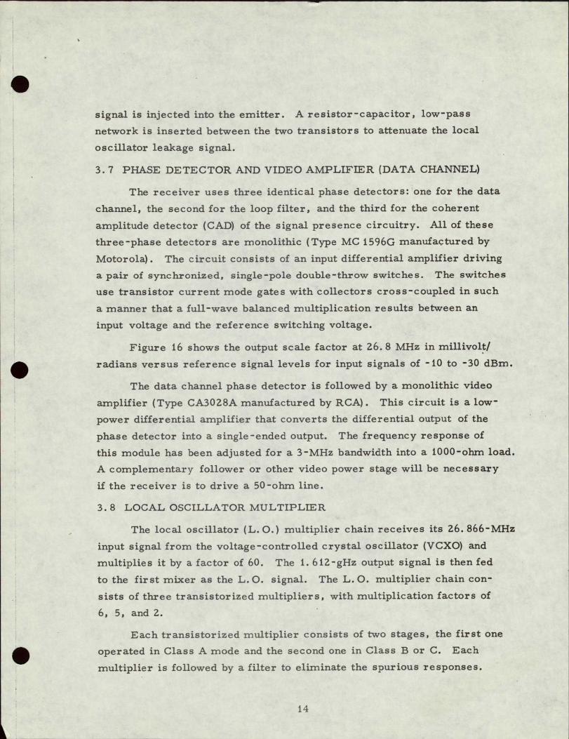
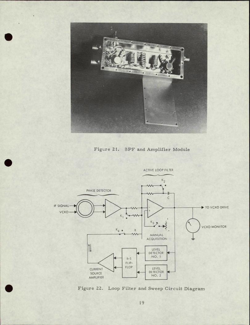
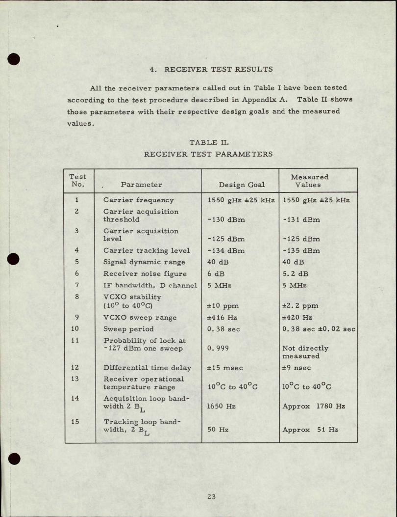

5 BINOR TEST RESULTS
The interface preliminary tests consisted of the L-band transmitter
modulation with the BINOR code or the 3 iZ kHz top tone transmission to
the receiver and processing of the receiver output
After the receiver AGC was adjusted the signal level into the
BINOR processor stayed within the acceptable limits for a wide range of receiver input levels The receiver output coupling capacitor needed to be increased because of an inadequate correlation level on the lowest subshy
frequency tone to the code processor
The receiver-to-processor interface also required close proximity of the two units because of the high output impedance of the receiver and may require receiver changes for impedance matching Printout of the processor output indicated that the system concept and method is practical
and feasible
Figure 29 illustrates the output of the receiver with three different
signal input levels In comparison to the upper two waveforms the sigshy
nal in the bottom portion of the photograph was completely buried within
the noise when adjusted for a minimum signal level but lock-in and proshycessing by the BINOR code processor were easily accomplished with no
errors
Figure 29 Video Output Waveforms
27
APPENDDC A
The test procedure for the L-band phase-lock
receiver is included in this appendix This procedure
explains the tests performed for the fifteen parameters
called out in the receiver specifications The block
diagram test setup the test equipment required and
the test procedure are given for each parameter
A-I
TEST PROCEDURE FOR THE L-BAND PHASE LOCK RECEIVER
Documentation required 1) Schematic L-Band Receiver SK68137
2) L-Band Phaselock Receiver Modules Interconnections SK68138
10 Carrier Frequency Figure A-1 shows one of the suggested RF source
configurations to test most of the receiver parameters
set-up
8614A HP
g Ge
1550 MHz L-Band
Phase Modulator
120 db P
at
arable3MHI
Atten
T
R
HP
Fre uency
I Synthesizer
F
IF Re
2650 P
Oscillator
Synthesizer
EH 122
Pulse Gen
Binor Gen
(or
Figure A- I
V
A-Z
11 Test Equipment Required Frequency Synthesizer HP 51008 Oscillator Synchronizer HP 2650A o Signal Generator HP 8014A o Pulse Generator EH 122 o Binor Code Generator (TRW) L-Band Phase Modulator (TRW) Calibrated Variable Attenuator HP 394A
12 Test Procedure
o Measure the frequency of the 8614A Signal Generator with
5245-L Electronic Counter Hp or equivalent
Make necessary adjustment to the IF reference frequency so
as to read a frequency of 1550 NHz from the Signal Generator o Record frequency reading on test data sheet
20 CARRIER ACQUISITION THRESHOLD 21 Test Equipment Required
RF Test source of Figure A-1 o Power meter HP 431C
22 Test Procedure o Measure RF power available at the input of the receiver with
431C Power Meter HP Add sufficient attenuation following the signal generator soO
as to decrease the available power at the output of the coaxial
calibrated attenuator to -81 dbm when the dial is reading 6 db o Turn the Mode Selector switch of the receiver to-165050 Hz
mode and set the calibrated coaxial attenuator to -145 dbm
output
Increase the RF power to the receiver from -145 dbm until the
receiver shows signs of threshold locking o Record carrier acquisition threshold level on data sheet
30 CARRIER ACQUISITION LEVEL
31 Test Equipment Required o RF Test source of Figure A-1
A-3
32 Test Procedure o Increase the RF power to the receiver to -125 dbm Receiver
should remain locked
40 CARRIER TRACKING LEVEL
41 Test Equipment Required a RF Test source of Figure A-i
42 Test Procedure
o Decrease the RF power to the receiver from -125 dbm to -134 dbm
Receiver should continue in locked condition
50 SIGNAL DYNAMIC RANGE
51 Test Equipment Required
o RF Test source of Figure A-I o Spectrum analyzer HP 851B85518
52 Test Procedure
o Connect spectrum analyzer to the 2nd IFamplifier output pin 5
o Set the RF test source to feed -130 dbm signal to the input
of the receiver o Set the spectrum analyzer in a narrow IFbandwidth to
observe the carrier signal
Increase the input signal to the receiver by 40 db Output
signal observed in the spectrum analyzer should remain
constant within 4 db
60 RECEIVER NOISE FIGURE
61 Test Equipment Required o Noise figure meter
o UHF Noise Source
o 10 db Pad
62 Test Procedure
HP 342A
HP 349A
o Set up equipment as shown in Figure A-2 Notice that the UHF Noise Source has a 10 db pad following removal
of this pad will damape the receiver Pre-amplifier
A-4
62 Test Procedure (continued)
o Adjust the zero and infinity adjustments of the noise figure meter
before taking a reading Noise figure should read between 5 to 6 db Record measurement on data sheet
r _ Noise Figure Meter f UHF Noise 10 db Receiver
I Source Pad Under Test
enHP-3A 349A HP I__--
I Is IFI_) _n_____---
IL
Figure A-2
A-5
3
2
50 Hz BANDWIDTH -124 dm INPUT
0
-1
-2
-3
-4
-5
-6
-7 L I I II
1 Ha 10 Hz 1000 H
Figure 28 50 Hz Mode Response
Z6
5 BINOR TEST RESULTS
The interface preliminary tests consisted of the L-band transmitter modulation with the BINOR code or the 3 iZ kHz top tone transmission to the receiver and processing of the receiver output
After the receiver AGC was adjusted the signal level into the BINOR processor stayed within the acceptable limits for a wide range of receiver input levels The receiver output coupling capacitor needed to be increased because of an inadequate correlation level on the lowest subshyfrequency tone to the code processor
The receiver-to-processor interface also required close proximity of the two units because of the high output impedance of the receiver and may require receiver changes for impedance matching Printout of the processor output indicated that the system concept and method is practical and feasible
Figure 29 illustrates the output of the receiver with three different signal input levels In comparison to the upper two waveforms the sigshynal in the bottom portion of the photograph was completely buried within the noise when adjusted for a minimum signal level but lock-in and proshycessing by the BINOR code processor were easily accomplished with no errors
Figure 29 Video Output Waveforms
Z7
APPENDIX A
The test procedure for the L-band phase-lock
receiver is included in this appendix This procedurq
explains the tests performed for the fifteen parameters
called out in the receiver specifications The block
diagram test setup the test equipment required and
the test procedure are given for each parameter
A-1
TEST PROCEDURE FOR THE L-BAND PHASE LOCK RECEIVER
Documentation required 1) Schematic L-Band Receiver SK68137
2) L-Band Phaselock Receiver Modules Interconnections SK68138
10 Carrier Frequency Figure A-i shows one of the suggested RF source set-up
configurations to test most of the receiver parameters
20 db 8614A HP 1550 MHz L-Band Pad I r9AeHl TO Sig Gen Phase Hl2 AttenW R
Modulator-A
S5100B HP R-2650A HP EH 122
Frequency IF Ref Oscillator Pulse Gen (orI Synthesizer _rSynthesizer Binor Gen
Figure A-1
A-2
11 Test Equipment Required o Frequency Synthesizer HP 5100B
o Oscillator Synchronizer HP 2650A o Signal Generator HP 8014A
o Pulse Generator EH 122 o Binor Code Generator (TRW)
o L-Band Phase Modulator (TRW)
o Calibrated Variable Attenuator HP 394A
12 Test Procedure o Measure the frequency of the 8614A Signal Generator with
5245-L Electronic Counter Hp or equivalent o Make necessary adjustment to the IFreference frequency so
as to read a frequency of 1550 MHz from the Signal Generator o Record frequency reading on test data sheet
20 CARRIER ACQUISITION THRESHOLD
21 Test Equipment Required o RF Test source of Figure A-I o Power meter HP 431C
22 Test Procedure Measure RF power available at the input of the receiver with
431C Power Meter HP o Add sufficient attenuation following the signal generator so
as to decrease the available power at the output of the coaxial calibrated attenuator to -81 dbm when the dial is reading 6 db
o Turn the Mode Selector switch of the receiver to-165050 Hz mode and set the calibrated coaxial attenuator to -145 dbm output
o Increase the RF power to the receiver from -145 dbm until the
receiver shows signs of threshold locking o Record carrier acquisition threshold level on data sheet
30 CARRIER ACQUISITION LEVEL
31 Test Equipment Required o RF Test source of Figure A-I
A-3
32 Test Procedure o Increase the RF power to the receiver to -125 dbm Receiver
should remain locked
40 CARRIER TRACKING LEVEL
41 Test Equipment Required o RF Test source of Figure A-i
42 Test Procedure
o Decrease the RF power to the receiver from -125 dbm to -134 dbm
Receiver should continue inlocked condition
50 SIGNAL DYNAMIC RANGE
51 Test Equipment Required o RF Test source of Figure A-i O Spectrum analyzer HP 851B8551B
52 Test Procedure Connect spectrum analyzer to the 2nd IFamplifier output pin 5
o Set the RF test source to feed -130 dbm signal to the input
of the receiver o Set the spectrum analyzer ina narrow IFbandwidth to
observe the carrier signal o Increase the input signal to the receiver by 40 db Output
signal observed in the spectrum analyzer should remain constant within 4 db
60 RECEIVER NOISE FIGURE
61 Test Equipment Required o Noise figure meter HP 342A
o UHF Noise Source HP 349A
o 10 db Pad
62 Test Procedure o Set up equipment as shown in Figure A-2
Notice that the UHF Noise Source has a 10 db pad following removal
of this pad will damage the receiver Pre-amplifier
A-4
62 Test Procedure (continued)
Adjust the zero and infinity adjustments of the noise figure meter
before taking a reading Noise figure should read between
5 to 6 db Record measurement on data sheet
Noise Figure Meter UHF Noise 10 db V Receiver HP 342A i Source Pad Under Test
349A HP
60 MHz Ist IF 1
Figure A-2
A-5
70 IF BANDWIDTH DATA CHANNEL
71 Test Equipment Required o Power Meter HP 431C
o Signal Generator HP 606C
72 Test Procedure O Reconnect the equipment as shown in Figure A-3 o Sweep manually the input frequency to the Ist IF and record
upper and lower frequencies resulting in 3 db drop from
the 62 MHz center frequency o The difference between the two readings is the bandwidth
of the IF data channel Record the bandwidth on data sheet
st IF 2nd Mixer amp Meter
Amplifier HP 431C
Signa88-866 Ref Osc
Generator 8 HP 606C
Figure A-3
A-6
80 VCXO STABILITY (100 to 40degC)
Data onthis test is available in Engineering Notebook No 8904
Examination of this data can be used to determine the VCXO stability
inlieu of an actual test
81 Test Equipment Required O Test oven
o Frequency counter HP5245L
o Precision power supply EPCO model
82 Test Procedures o Connect equipment as shown in Figure A-4
OVEN
I co IVCXO Frequency 12V Under Counter
Test -
I - - Cwnt~or Voltage
IPrecision PS
Figure A-4
o Vary the temperature of the oven from OdegC to 500C in 10 degree
intervals 0 For each temperature setting vary the control voltage from
+1 to +7 in steps of I volt o Record and tabulate the data
A-7
90 VCXO SWEEP RANGE The receiver has been designed with a sweep range of + 25 kHz The VCXO preceeds a times 60 multiplier chain therefore the actual deviation of the VCXO is 160 of + 25 kHz or + 416 Hz From the data taken inparagraph 8 the scaling factor (approximately
416 Hzvolts) can be obtained The amplitude of the sawtooth waveform sweeping the VCXO determines the sweep range
91 Test Equipment Required o Osci-loscope Tektronix 585
92 Test Procedure o Connect oscilloscope to test point marked TP on the
Loop Filter and Sweep Circuit module o Measure peak-to-peak amplitude of the sawtooth waveform o Calculate and record the sweep range
100 SWEEP PERIOD
101 Test Equipment Required o Oscilloscope Tektronix 585
102 Test Procedure o Connect oscilloscope to test point TP of the loop filter and
sweep circuit o Measure and record the sweep period
110 PROBABILITY OF LOCK (-127 dbm) on one sweep A direct measurement of probability of lock requires several thousands locking operations and a correlation of the compiled data into a single
number
Probability of lock of 0999 becomes very difficult to measure and beyond the scope and capabilities of this program therefore this
test cannot be performed at this time
It is important to notice that the probability of acquisition is a function of several parameters such as signal to noise ratio threshold
sensitivity dampinq factor sweep rate loop bandwidth etc
A-8
It has been demonstrated ()that the smaller the ratio of sweep rate
and loop noise bandwidth the greater is the probability of lock for
a given signal to noise ratio and damping factor
The ratio just mentioned is 0046 for this receiver and it is
obtained as follows
ratio = R = 25xi0 302 = 0046 (1650)2(Bno)2
Figure 3 of the referenced paper shows that the probability of lock
for a 10 db SN and damping factor of 07 is 95 when this ratio
is 012 Therefore the 0046 ratio is an assurance that the
probability of lock is better than 95
120 DIFFERENTIAL TIME DELAY
121 Test Equipment Required o AD-YU 202 Vectorlyzer
o Binor Code Generator
o Binor Processor
122 Test Procedure
o Connect the system as shown in Figure A-5
JP Frazier and J Page Phase Lock Acquisition Study
IRE Trans on Space Electronics and Telemetry page 211
figure 3 September 1962
A-9
Binor CodeGenerator II
600 Binor ohms
code
AD-YU 202 Vectorlyzer
E2 El
Binor I
Processorr_- - -Li0sc
IHFDiv Card LI
Car
H
R-F ~~20db Rcie
Source -
L-Band Phase
Modulator___ Pad - -
Variable Attenuator
Receiver Under TestL _Video
Figure A-5
122 Test Procedure (Continued)
0 Set the Binor Code Generator switches as follows
Mode Switch to CW
Clock Switch to RUN
OUT Switch to NORM
OscSel Switch to INT
Gate Switch to INT
AC Power Switch to ON
deg Adjust the Vectorlyzer per manufacturer procedure on the 0-180 deg scale
bull LFIP supplies a 300 kHz signal from the binor processor oscillator which
is phase locked to the fundamental of the video output of the receiver
providing a noise-free signal for use in the differential time delay A
measurement
A-10
122 Test Procedure (Continued) o Set the RF attenuator for -121 dbm signal to the input of the
receiver and note the phase difference o Increase signal to the receiver to -81 dbm Note the maximum
phase deviation from step above
Multiply maximum phase deviation observed in step above by 925 nsec
per degree The resulting value isthe absolute value of differential
time delay
O
130 RECEIVER OPERATING TEMPERATURE RANGE TEST
131 Test Equipment Required deg Test oven for 100C to 400
o Frequency source set-up as per Figure A-I
132 Test Procedure Place receiver inthe oven and set temperature to 10C After
20 minutes at that temperature check carrier acquisition threshold
O
o Repeat above step for temperature of 20 30 and 400C
deg All the preceeding tests should show a -130 dbm carrier acquisition
threshold or better Record test in data sheet
140 ACQUISITION LOOP BANDWIDTH (2BLs 1650 Hz)
141 Test Equipment Required O Signal Generator HP 8614A
O Oscillator Syncronizer HP 2650A
o Frequency Synthesizer HP 5100B 0 Synthesizer Driver HP 5110B
Dual DC Power Supply HPHarrison 6205B
0 Pin Diode Switch Modulator
Waveteck III Voltage Controlled Generator
o DC Power Supply HP 721A
o Oscilloscope Tektronix 453
Variable Attenuator HP 394A
O 20 db Pad
0
O Wave Analyzer HP 302A
o AC Transistor Voltmeter HP 403A
o Oscilloscope Tektronix 585
A-11
141 Test Equipment Required (Continued) Transmitter Assembly Test Set-up o Connect the transmitter assembly as shown in Figure A-6 o Set the following switches to the indicated position
Tektronix 453 Oscilloscope
Power switch to ON Vertical 2 Vcm DC
o Waveteck III VC Generator
Power switch to Xl
Output selector to Sine wave
o HP 721A Power Supply
Power switch to ON
Voltage adjust pot to -55 VDC (seen on the 453 oscilloscope) o Harrison 6205B Dual Power Supply
Power switch to ON (Modulator power switch should be OFF)
Both Voltage pots to 20 volts DC Wiring should be set up to provide both +20V and -20 volts to the modulator
o Modulator
Power switch to ON
o HP 8614 Signal Generator
Line switch to ON
RF switch to ON
ALC switch to ON Ext FM switch to ON
DBM meter to 0 Attenuation dial to -045 db Frequency dial to 1554 MHz
o HP 5100B HP 5110B Synthesizer
Power switch to operate (both 5100B and 5110B)
Frequency standard switch to INT Frequency selection switch to Local Keyboard Frequency Keyboard switch to 3001005000 Hz Search control switch to Remote
A-12
INSIDE SCREEN ROOMOUTSIDE SCREEN ROOM
HPHarrlson + Modulator 0 Variable ttn Output
6205 B Dua Pwr Sup 20V
0db Port 3PadTo
inpU Attenuator
HP 394A
to Output Receiver
-Video I n shy -
Calib
RF Out
HP 8614A Signal Gen
xt FM Uncal
5 Inc_ - - -
SIF tReAflnu
Y ntsc Tektronix 453
HP 2650 Oscilloscope
Output HP 5100B
Wavetek III VC Gen
SynthesizerAssembly Search --
J output
NOTE Use caution with the
Control Control___ -
ground wiring This generator is operated at an elecated DC level
HP 721A Power Supply
Figure A-6
141 Test Equipment Required (Continued)
o HP 2650A Synchronizer
Power switch to ON
IF Mode switch to EXT
APC switch to ON
Search light should be OFF
Phase meter should be slightly off center This is
accomplished by adjusting the HP 8614A signal generator
frequency
o HP 394A Variable Attenuator
Set the variable attenuator control dial to read 49 db of attenuation (This provides a power into the receiver
of -124dbm)
Allow a 30 minute warm up period before conducting test
Receiver Test Set-up o Connect the receiver assembly as shown in Figure A-7 o Set the following switches to the indicated positions
o HP 403A AC Transistorized Voltmeter
Range switch to 0 db ( 1V RMS full scale)
Function switch to 1 cps - 1 Mc
o Tektronix 585 Oscilloscope
Power switch to ON
Vertical to 1 Vcm DC
o HP 302A Wave Analyzer
Power switch to ON
Scale Value switch to Absolute
Mode selector switch to Normal
o L-Band Phase Lock Receiver (Unit under Test)
Power switch to ON
Allow a 30 minute warm-up period before conducting tests
142 Test Procedure 1650 Hz Noise bandwidth
o The HP 302A Wave Analyzer should be connected to point reg in figure 7 The Mode Selector switch on the receiver should be
in the 1650 Hz AUTO position Set the frequency of the Wavetek Ill oscillator to 250 Hz
A-14
Transmitter Assembly Output from Variable Attenuator
L-Band Phaselock Receiver
Loop Filter and Sweep Circuit
PinLH[OI6 TPI
1
IInput
HP 302A Wave Analyzer
Output
4 input
HP 403A AC Trans-istorized Voltmeter
4 vent-in
Tektronic 585 Oscilloscope
Ficure A-7
Vary the ATTEN control on the Waveteklll oscillator and the
FREQ Keyboard setting of the HP 5100B FREQ Synthesizer until
a reading of -40 db is observed on the HP 302A wave analyzer meter (The Frequency control on the Wave Analyzer will need to be adjusted
for a peak at 250 Hz and the MODE Selector set to AFC) The
proper setting of the FREQ Keyboard will be one of the following
settings 3 0 0 1 0 0 0 50 0 Hz
3 0 0 1 0 0 5 00 0 Hz
3 0 0 1 0 5 0 00 0 Hz
3 0 0 1 5 0 0 00 0 Hz
O Note the signal level in db for various frequencies ranging
from 10 Hz to 2 kHz The procedure for this isto set
the frequency of the Wavetek 111 oscillator to the desired
setting Set the MODE selector on the wave analyzer to NORMAL Adjust the Wave Analyzer Frequency control until a peak
isobserved then replace the MODE Selector to AFC Read the signal
indb directly from the Wave Analyzer meter Compare this data
with figure 3-3 inreference No 1 in order to determine the
damping factor and the loop resonate-frequency
150 TRACKING LOOP BANDWIDTH (2BL) 50 Hz)
151 Test Equipment Required o Same as paragraph 141
Transmitter Assembly Test Set Up 0 Same as paragraph 141
Receiver Test Set Up o Same as Paragraph 141
152 Test Procedures 50 Hz Noise Bandwidth 0 The HP 302A wave analyzer should be connected to point Q
infigure 7 The mode selector switch on the receiver should be inthe 165050 Hz AUTO position Set the frequency of the Wavetek Ill oscillator to 10 Hz
A-16
152 Test Procedures 50 Hz Noise Bandwidth (Continued) 0 Using the procedure of paragraph 142 second item obtain a meter
reading of -10 db at a frequency of 10 Hz Adjust the OUTPUT AMP
pot on the Wave Analyzer until the HP 403A AC transistorized
voltmeter reads 0 db Note The range of this meter is now identical to the range of the
Wave Analyzer This setup may be used down to the frequency
of 3 Hz It should not be used below 3 Hz and at this frequency 1 db should be added to the meter reading At 4 Hz and above
the meter may be read directly o Using the procedure of paragraph 142 third item obtain the signal
level for various frequencies ranging from 3 to 30 Hz The signal should be read in db from the HP 403A voltmeter The
Tektronix 585 scope is provided to aid in the peaking of the signal Compare this data with figure 5-1 in reference No 1
in order to determine the loop resonate frequency o The HP 302A Wave Analyzer should be connected to point reg
in figure 7 The Mode Selector switch on the receiver should be
in the 165050 Hz AUTO position Set the frequency of the Wavetek Ill oscillator to 10 Hz
o Using the procedure of oaragraph 142 second item obtain a
meter reading of -70 db at a frequency of 10 Hz Usini the procedure of paragraph 152 second item calibrate the HP 403A Voltmeter
o Using the procedure of paragraph 142 and 152 third items obtain
the signal level for various frequencies ranging from 3 Hz to 100 Hz Compare this data with figure 3-3 of reference No I to obtain the damping factor
Reference No 1 Theory of Phaselock Techniques as applied to Aerospace
Transponders Floyd M Garner and Steven S Kent
Contract No NAS8-11509 Marshall Space Flight Center
NASA Huntsville Alabama
A-17
APPENDIX B
The modules interconnections diagram is
included to serve as an aid in receiver maintenance
All cabling is coaxial with the exception of the
color-coded power supply wiring meters and
selector switches
B-1
_ 7 643 2
CK PANEL) VIDEO OUTPUT
PRESELECTOR PRE-AMP POST IT IF 2ND MIXER s VIDEO AND SLCF
VIDEOOUPUM (BACKPANEL)
IN INIIGNNAG
STRENGTH MS3IO2ELIOSL-3P P
(FRONT PANEL
N(FON) OFF SWITCH (FRONT)N MLTIPIERMULIPIE -V-12V -GD PAAINALP(FPANEAMD-PL PRESENCE
FUSE HOLDER (BACK) + 3- CAD TEST C
POWER SUPPLY
1212 050050IG REL
L - VCXO AI
+12V LOOP FILTER AND - I aV G O -2 SWE EP C T
R3
-6D VCXCMONITOR -J-I
-6 -6 -12 -12I
MNUAL ACQUISITION CFRONT PANEL) regMODE SELECTOR
(FRONT PANEL) B
4M2v
WIRING OQORCOD
REGULATOR CARD ING RED ___________
-22V BLUE
4 6 ORANGE _ _
A -6VI PURFLEI --__
GND BLACK L BAND PHASELOC
O 1650 MAN shy16 50 HI AUTO-165050 AUTO RCEINTER N
-I-ULES INTERCONNECTIONS
NOTESUNLESSOTHERWSS SPECIFWM
ri I I 5 ~ h~T
APPENDIX C
ALIGNMENT
REQUIRED TEST EQUIPMENT
The following test equipment
for performing these tests
Sweep Generator
CW Generator
Oscilloscope
Attenuator
Spectrum Analyzer
Power Meter
RF Detector-
Synchronizer
Synthesizer
Modulator
Power Supply
Loads
DC Milliamp Meter
Pulse Generator
PROCEDURE
AND TYPICAL TEST SET UP
or its equivalent should be on hand
Jerrold model 900C HP 8690A with 8691A plug-in
HP 606 50 kHz to 65 MHz HP 608 10 MHz to 480 MHz HP 642 450 MHz to 1230 MHz HP 8614A 800 MHz to 2400 MHz
Tektronix 453 Tektronix 585 with (CA type plug-in)
OSM model 20510-3 (3 db) fixed OSM model 20510-6 (6 db) fixed OSM model 20510-10 (40 db) fixed HP 394A (6-140 db) variable HP 8491A - 20 db (20 db) fixed HP 8491A - 10 db (10 db) fixed
HP 851B8551B
HP 431C with 478A thermistor
HP 423A
HP 2650A with 105 3333 MHz crystal
HP 510OB5110B
TRW Bi phase
HPHarr-ison 6205B (dual) (3 each) EPSCO VRS 611 HP 7Z1A
50 ohm OSM 20140P (4 each)
Simpson model 269
EH 122 TRW Binor code generator
C-I
Voltage Controlled Generator- Wavetek model 111
Frequency Counter HP 5245L with 5253 andS54 plug-in
Voltmeter HP 3430A
Noise Figure Meter HP 342A with the HP 349A UHF Noise Source
AC Voltmeter HP 403A (no equivalent)
Wave Analyzer HP 302A (no equivalent)
OUTSIDESCREEN INSIDE SCREEN ROOM
R-- 12V MODULATOR RSNI INTUTF MIABLE ATTNOUTPUT
DUA S P
HP TORECEIVER
Hp8614AISIGNALGENERATOR EXT FM UNCA
IPT RFO U
USECAUTION WITHTHE4535 GROUNDWRING mUSGENERATORIS OPERATED
C ATAN ELECATEDDC LEVEL
OUTPUTHP 510BKII SYNTHESIZER
ASSEMEampy
SEARCH
CONTROL
Figure 1 Transmitter Assembly Test Set-Up
The following test set-ups will be referenced frequently throughout
this procedure
1 1 RIF Test Set-Up
The R F Test Set-Up is illustrated in Figure 4 This set-up will
be used for the following modules
Pre-selector Pre-amplifier Post selector First IF amplifier Second mixer and second IF amplifier Narrowband filter L 0 multiplier
C-a
Each section of this test procedure will specify the connections used
(regthroughreg)or not used and the frequencies and power levels
associated with each connection From this the test equipment may be
easily selected from the provided list
In all sections of this test procedure the RF connections on the test
unit must be terminated into 50 ohms It is recommended that an
attenuator ( 3 to 10 db) or a 50 ohm load be placed on all connectors in
order to insure the proper load impedance and reduce cable effects
It is also recommended that all cables be kept as short as practical
It will be noted that when swept measurements are made then the
sweep generator the REF detector and the oscilloscope are used When
a GW measurement is made the CW generator is used in conjunction
with either the spectrum analyzer or the power meter Allow a 30
minute warm up before conducting tests
SIGNAL GNRIKOSCOPE
GENERATOR ENERATOR
DACPO
C-Figur 2NRUTetStU
SDC POWER
SUPPLIES
DC MILLIAMP
METER
EPSCOVRS 611
VCXODRIVE
UNITUNDER OUTPUT AEN SETUANALYZER
ADDITIONAL OUTPUTS POWER
Figure 3 Oscillator Test Set-Up
1 2- Oscillator Test Set-Up
The Oscillator Test set-up Is illustrated in Figure 3 This set-up
will be used for the following modules
Reference Oscillator VCXO and Buffer
Each section of this test procedure will specify the connections
used (regthrough) or not used and the frequencies and power levels
associated with each connection From this the test equipment may be
easily selected from the provided list
In all sections of this test procedure the RF connectors on the test
unit must be terminated into 50 ohms It is recommended that an
attenuator (3 to 10 db) or a 50 ohm load be placed on all connectors in
order to insure the proper load impedance and reduce cable effects It
is also recommended that all cables be kept as short as practical
Allow a 30 minute warm up before conducting tests
C-4
131
1 3 Transmitter Assembly Test Set-Up
Connect the transmitter assembly as shown in Figure 1
Set the following switches to the indicated position
Tektronix 453 Oscilloscope
Power switch to ON
Vertical Z Vcm DC
Waveteck III V C Generator
Power switch to Xi
Output selector to Sine wave
HP 721A Power Supply
Power switch to ON
Voltage adjust pot to -5 5 VDC (Seenon the 453 oscilloscope)
Harrison 620513 Dual Power Supply-
Power switch to ON (Modulator power switch should be OFF)
Both voltage pots to 20 volts DC Wiring
should be set up to provide both +Z0V and
-20V to the modulator
Modulator
Power switch to ON
HP 8614 Signal Generator
Line switch to ON
RF switch to ON
ALC switch to ON
Ext FM switch to ON
DB2A meter to 0
Attenuation dial to -045 dB
Frequency dial to 1554 MHz
tests only it will be called for inThis equipment is used for specific the procedure if required
C-5
HP 510GBHP 5110B Synthesizer
Power switch to operate (both 5100B and 5110B)
Frequency standard switch to INT
Frequency selection switch to Local Keyboard
Frequency Keyboard switch to 30010000 00 Hz
Search control switch to Local
Pulse Generator
Power Switch to ON
HP 2650A Synchronizer
Power switch to ON
IF Mode switch to EXT
APC switch to ON
Switch light should be OFF
Phase meter should be slightly off center This is accomplished by adjusting the HP 8614A signal generator frequency
HP 394A Variable Attenuator
Set the variable attenuator control dial to read 49 dB of attenuation (This provides a power into the receiver of -424 dBm)
Allow a 30 minute warm up period before conducting test
1 3 Z Transmitter Frequency Adjustment
Connect the counter to the output of the HP 8614A and adjust the
HP 5100B synthesizer frequency until the counter reads 4550 000 MHz
Reconnect the signal generator output to port I of the modulator
133 Power Calibration Procedure
Temporarily remove the 20 dB pad and set the variable attenuator to -10 dB
Connect the HP 431C power meter to point reg (Figure 1)
This equipment is used for specific tests only it will be called for in the procedure if required
c-6
Adjust the variable attenuator on the HP 8614 (oscillator) until -25 dBm is observed on the power meter
Replace the 20 dB pad and add 40 dB to the HP 8614 (oscillator) variable attenuator
The system is now calibrated so that the power input in -dBr to
the receiver is the sum of the HP 394A attenuator reading plus 75
2 SUBASSEMBLY ALIGNMENT PROCEDURES
Ten modules of the L-Band receiver require bench alignment
prior to receiver system test The remaining modules are tested and
aligned utilizing the receiver noise
2 1 Pre-Selector Test Procedure
Utilize the RF test set up of paragraph 1 1 and Figure 2
Connections Approximate requirements
reg input 1 55 GHz at -10 dBn
output 1 55 GHz at -10 dBm
copy (E) and ( un-used
This is a high pass filter It should have an insertion loss of less
than 4 dB and greater than 60 dB loss at 400 MHz The only adjustment
possible in this module is to replace the capacitors or change the length
of the inductors
2 Z Pre-Amplifier Test Procedure
Utilize the RF test set up of paragraph 4 1 and Figure 2
Connections Approximate requirements
reg input 4 55 GHz at -50 dBm
G output 4 55 GHz at -30 dBm
copy D and un-used
DC power +1Z 0 VDC at 10 ma
C-7
2
There is no provision for adjustment of this module It is a wideshy
band preamplifier with only the requirements that the gain at 1550 MHz
be greater than 15 dB that the 3 dB bandwidth be greater than Z0 MHz
(+ and -10 MHz) and that the noise figure be equal to or less than 5 dB
The gain and bandwidth may be tested on this set up however the
noise figure will be tested during the receiver front end alignment
(section 3 2)
CAUTION The preamp contains open circuitry and transistors Do
not touch the substrate or any part in this box
2 3 Post Selector Test Procedure
Utilize the RF test set up of paragraph I 1 and Figure Z
Connections Approximate requirements
G input 45 GHz at -40 dfm
output 1 55 GHz at -40 dBm
un-used
This is a bandpass filter that has an insertion loss of 2 dB or less
and a bandwidth greater than 20 MHz (+ and -40 MHz) at the 3 dB points
The image frequency range (1 665 to 4 675 GHz) must be greater than
20 dB down
The two capacitors should be adjusted with the unit set up in the
swept mode and the CW mode should be used to check the specifications
2 4 1st IF Amplifier Test Procedure
Utilize the RF Test set up of paragraph I I and Figure Z
Connections Approximate requirements
reg input 62 MHz at -80 dBm
output 62 MHz at -10 dBm
Sand reg un-used
AGC input 0 VDC (min gain) to 1 8 VDC (maximum)
DC input +6V at 55 ma
C-8
This high gain amplifier should have a gain of approximately 70 dB
at the center frequency of 62 MHz and a 3 dB bandwidth of 6 MHz (+3 and
-3 MHz) The AGC should have control over a dynamic range of 40 d3
The capacitor (C10 and CI) should be adjusted with the unit in the
swept mode with the AGO voltage set to approximately 1 5 VDC It may
be necessary to select C-19 the coupling capacitor (between C-10 and
C-11) for the proper bandwidth (a larger capacitance causes a narrower
bandpas s)
With the unit in the CW mode apply 26 8 MHz at about -40 dBm
to the input and adjust C-9 and C-16 for a null of the 26 8 MHz signal
at the output Reset the input signal to 62 MHz at -80 dBm and adjust
the AGOC voltage for maximum gain Repeat these adjustments until
satisfaction is achieved
Make a plot of gain versus AGO voltage to insure that the AGC
voltage has a 40 db dynamic range Connect the spectrum analyzer to
the IF output Insure that there is no spurious oscillation while varying
the AGC voltage from 0 to 2 0 volts
Z 5 Znd Mixer and Znd IF Amplifier Test Procedure
Untilize the RF Test set-up of paragraph 1 1 and Figure 2
Connection Approximate requirement
signal input 62 MHz at -50 dBm
O output 4
reference oscillatoinput
r
268 MHz at-4 (35 dB gain)
88 86 MHz at -5
5 dBm
dBm
unused
output 5 Z6 8 MHz at -19 (31 dB gain)
dBm
0 DC power +12 0 VDC at 20 ma +6 0 VDC at 24 ma
This unit should have a gain of approximately 35 db at output 4
and 31 db at output 5 The bandwidth should be 5 MHz at the 3 db points
(+Z 5 MHz and -Z 5 MHz) centered at 26 8 MHz
C-9
Set up the approximate bandwidth first by removing the reference
oscillator input (point ) and setting up the sweep generator at 268 MHz
Adjust C-4 and C-8 for the approximate bandpass Now reconnect the
reference oscillator and set the sweep generator to 62 MHz Adjust
C-4 and C-8 until the desired bandpass is achieved It may be necessary
to select C-5 for the proper bandwidth (a larger capacitance caupes a
narrower bandpass)
With the test set-up in the CW mode and the spectrum analyzer on
the output (4 or 5) insure that the proper gain is achieved at 26 8 MHz
If the conversion efficiency is bad it will be seen by a relatively low
signal at Z6 8 MHz and a relatively high signal at 6Z MHz If this
efficiency is poor it may be required to change the two resistors on pin
5 of the MC 155OG (mixer) Also verify that there are no spurious
oscillations observed on the spectrum analyzer
2 6 Narrowband Filter Alignment
Utilize the RF test set-up of paragraph 1 1 and Figure 2
Connection Approximate requirements
G input 268 MHz at -24 dBm
G output 4 26 8 MHz at -24 dBm
unused
output 5 26 8 MHz at -29 dBm
DC power +12 0 VDC at 20 ma
This narrowband amplifier should have a gain of 0 dB at output
4 and a loss of 5 dB at output 5 The bandwidth should be 500 kHz
(+250 kHz and -250 kHz) at the 3 dB points centered at 26 8 MHz
For swept measurements it may be necessary to increase this power to about -10 dBm in order to have an observable signal However the bandshywidth should be set such that it is correct for a CW test that is performed at -24 dBm
C-10
Connect the test set up in the swept mode and adjust the bandpass
of the filter Adjustments are made by squeezing or separating the turn
of L-3 L-4 and L-5 Next connect the test set-up in the CWmode and
verify the bandpass and gain Also verify that there are no spurious
oscillations seen on the spectrum analyzer
2 7 Reference Oscillator Alignment
Utilize the oscillator test set-up of paragraph 1 2 and Figure 3
Connections Approximate requirements
)unused
output unit 1 88 866666 MHz at -5 dBm
unit 2 amp3 88 861666 MHz at -5 dBnm
DC power -4Z 0 VDC at 3 ma
Adjust C-3 for the proper frequency as observed on the counter
Monitor the output on the power meter and observe the -5 dBm on the
power meter It may be necessary to add a resistor (45K or greater)
from pin 10 of the flatpack to ground in order to increase the output
power Monitor the output on the spectrum analyzer and verify that
there are no spurious oscillations
Repeat the above tests with the unit in an environmental temperature
chamber Over the temperature range of +400C to +400C the frequency
change should be less than 10 PPM (886 Hz)
2 8 VCXO and Buffer Alignment
Utilize the oscillator test set-up of paragraph 4 2 and Figure 3
Connections Approximate requirements
VCXO drive 3 VDC to 9 VDG nominal to 6 VDC
Q and outputs 26 866666 MHz at -11 dBm
D DC power -Z 0 VDC at 16 ma
NOTE All tests on this device are performed with the oscillator output (OUT) connector connected to the buffer input (IN) connector through a short piece of coaxial cable Any one of the buffer outputs (output 4 thru 4) are then measured
C-l1
Select R-11 to the 9 05 K ohms
Set the VCXO drive voltage to 6 0 VDC and adjust C-3 until the
proper frequency (26 866666 I-z) is observed on the counter Monitor
the outputs (i thru 4) with the power meter and verify that they are at
-11 dBm It may be necessary to add a resistor (15 K or greater) from
pin 10 of the flatpack to ground in order to increase the output power
Make a graph of the frequency versus VCXO drive voltage of 3 OV to
9 OV Verify that the slope of this curve (VCXO scale factor) is about
400 Hzvolt Connect the output to the spectrum analyzer and verify that
there are no spurious oscillations
Repeat the above tests with the unit in an environmental temperature
chamber Select R-11 until the change in frequency between the tempershy
ature of 40 0C and 400C at any VCXO drive voltage (3 CV 6 0V or 9 OV)
is less 10 PPM (268 Hz)
Repeat the above tests until the satisfaction is achieved
2 9 L 0 Multipher (X 60) Alignment
CAUTION Due to the non-linear elements and the high frequencies associated with frequency multipliers it is not recomshymended that this adjustment be performed outside of the factory Should this procedure be attempted it is essential that it be performed under laboratory condishytions utilizing the proper test equipment and pershysonnel that have extensive knowledge of RF techniques and experience with Varactor multiplier adjustment This document is written as a guide to the qualified technician not as an absolute step-by-step procedure
2 9 1 Preliminary Set Up Considerations
The multiplier should be energized with +iZ 0 volts DC (the case
is ground) The typical DC current for the whole unit is about 30 ma
therefore a current limited supply at about 50 ma should be used
The unit is composed of 4 parts 3 RF cards and one comb-hne
filter (see Figure 4) Preliminary adjustments on each of the 3 cards
should be made individually These adjustments are discussed in
sections Z 9 Z 2 9 3 and 2 9 4 The set-up for each of these sections
is to solder on a coaxial cable to the input and output of the card having
C-1Z
removed the original connection and terminate these cables into 50 ohm
impedance It is recommended that each coax be kept short and that a
50 ohm attenuator (3 to 10 db) be placed as close to the card as possible
SEE NOTE -- --BELOW ---
X2 X5 X2 MULITPLIER MULITPLIER MULTIPLIER
CARD CARD CARD INPUT OUTPUT OUTPUT OUTPUT
IN PUTTOUPU COMBLINEINPUT[ FI[Z]PLTER
INPUT OUTPUT INPUT OUTPUT
GND DC INPUT
NOTE DO NOT SOLDER TO THE COMB-LI NE (MICRO-STRIP) FILTER CONDUCTIVE EPOXY MUST BE USED HERE
Figure 4 Multiplier Configuration
Final adjustment of the unit must be accomplished with the unit
completely assembled _ and that the input and output connectors be
terminated into 50 ohms It is recommended that an attenuator
(3 to 10 db) be placed on the input and output connector in order to insure
proper impedance matching and reduce cable effects
NOTE DO NOT solder to the comb-line (micro-strip) filter Conductive epoxy must be used here
C-13
The typical test set up is illustrated in paragraph 1 1 and
Figure 2 This set-up should be used whether the test unit is only one
card or the entire multiplier unit The only precaution necessary is that
the test equipment will supply the required input frequencies and power
levels and that the test equipment is linear at the output frequencies and
power levels These data are given in Table 4
Table I InputOutput Requirements
Input at Connection Output at Connection G
Unit Frequency Power at PT A Frequency Power at PT BMHz dbm (50 ohmF MHz drn (50 ohmT
X6 269 -10 161 -95
X5 161 -95 806 0
XZ 806 0 1612 +10 0
X60 269 -40 1612 +100
Connection Approximate Requirements
Bampa)Unused
DC Power +12 0 VDC at 30 ma
2 9 2 X6 Multiplier Card Adjustment
The test set-np should be connected in the CW mode utilizing the
spectrum analyzer as an indicator Tune C5 C8 C10 C12 and C11
for a maximum signal at 161 MHz Be sure that the signals at 133 MHz
(X5 mode) and 187 MHz (X7 mode) are as low as possible
The test set-up should now be changed to the swept mode and the
same capacitors adjusted until a pleasant band pass is observed that is
about 7 MHz wide at the 3 dB points (relative to output frequency)
Repeat the previous two paragraphs until a satisfactory bandpass
is achieved and all spurs and harmonics noted in the first paragraph
are about 60 dB below the carrier
C-14
Next connect the test set-up in the CW mode with the power meter
as an indicator The power out should be -10 dBm If this is not satisshy
factory adjust R2 or Ri until satisfaction is achieved
Again repeat all previous paragraphs of this section until satisfaction
is achieved
It should be noted that C5 adjusts the resonance of the input circuit
whereas C8 C10 and C12 each adjust the resonance of one pole of the
3 pole filter in the output circuit Adjustment of C11 changes the impedance
loading that the filter sees and thus it adjusts the filters coupling and
shape Adjustment of RZ and R1 change the transistors bias voltage so
that the transistor Q will be operating at its most optimum point (class B)
for multiplication
Z 9 3 X5 Multiplier Card Adjustment
The test set-up should be connected in the CW mode utilizing the
spectrum analyzer as an indicator Tune C18 CZI CZ5 CZ7 and C26
for a maximum signal at 806 MHz Be sure that the signals at 644 MHz
(X4 mode) and 965 MHz (X6 mode) are as low as possible
The test set-up should now be changed to the swept mode and the
same capacitors adjusted until a pleasant bandpass is observed that is
about 35 MHz wide at the 3 dB points (relative to output frequency)
Repeat the previous two paragraphs until a satisfactory bandpass
is achieved and all spurs and harmonics noted in the first paragraph
are about -47 dB below the carrier
Next connect the test set-up in the OW mode with the power meter
as an indicator The power out should be at 0 dBm If this is not
satisfactory adjust R4 or R7 and R9 or R8 until satisfaction is achieved
Again repeat all previous paragraphs of this section until satisshy
faction is achieved
It should be noted that C18 adjusts the resonance of the output
circuit of the input (161 MHz) amplifier QZ R4 and R7 adjust the bias
voltage of this class A amplifier and thus adjusts its gain R9 and RI0
adjust the bias voltage of the multiplying transistor Q3 so that it will be
C-15
operating at its most optimum point (class B) for multiplication CZI
CZ5 and C27 each adjust the resonance of one pole of the 3 pole filter
in the output circuit C26 adjusts the loading impedance seen by the
filter thus adjusting the filters coupling and shape
Z 94 XZ Multiplier Card Adjustment
The test set-up should be connected in the CW mode utilizing the
spectrum analyzer as an indicator Tune L9 and C36 for a maximum
signal at 1612 MHz Be sure that the signals at 806 MHz (XI mode)
and Z418 MHz (X3 mode) are as low as possible
L9 is adjusted by changing the length of the coil This usually
involves unsoldering the coil changing it then resoldering it back in place
repeated soldering may damage the circuit board therefore this procedure
should be done as few times as possible
The test set-up should now be changed to the swept mode and the
same elements adjusted until a pleasant bandpass is observed that is
about 140 MHz wide at the 3 db points (relative to output frequency)
Repeat the previous two paragraphs until a satisfactory bandpass
is achieved and all spurs and harmonics noted in the first paragraph are
about 27 db below the carrier
Next connect the test set-up in the GW mode with the power meter
as an indicator The power out should be equal to or greater than +10 dbm
If this is not satisfactory adjust R13 or R1Z and R16 or R17 until satisshy
faction is achieved
Again repeat all previous paragraphs of this section until satisshy
faction is achieved
It should be noted here the L9 adjusts the resonant point of the
output circuit of the input (806 MHz) amplifier Q4 whereas R13 and
R1Z adjust the bias voltage of this amplifier (class A) R16 and R17
adjust the bias voltage for the multiplying transistor Q5 such that it is
operating at its optimum point (class B) for multiplication C35 adjust
the output tank of this circuit
c-16
2 9 5 Total Multiplier Alignment
It is essential that the technician follow three basic principles when
adjusting the total unit
First Always understand exactly what he is adjusting in terms
of circuit element electrical element and expected response
i e C10 adjusts the center pole of the 160 MHz filter and
should cause the response to increase in amplitude and become
flat when properly adjusted
Second- Only make very small changes at any one time A large
change could cause an erroneous indication i e a large
change in C21 could cause the X5 multiplier to operate better
as a X4 and the swept bandpass look improved however the
change in output frequency would go un-noticed
Third Always use proper ftF techniques
The unit should be set up in the swept mode and the following
adjustments performed while looking for the highest-most pleasant
looking bandpass
1 Adjust the two capacitors of the comb line (microstrip) filter along with C36 This is to align the output filter and the output tank of the X2 multiplier card
2 Next adjust the input tank C5 to insure input impedance matching
3 Next adjust CZ7 CZ5 and CZ to insure the alignment o of the 800 MHz filter
4 Next adjust C12 CI0 and C8 to insure the alignment of the 460 MHz filter
5 Then adjust C8 to insure the alignment of the 160 MHz
amplifier
6 Steps 1 through 5 should be repeated
7 Then adjust coupling capacitor C26 to flatten out and widen up the response C27 will need to be adjusted to bring the filter pole back to its proper position
C-17
8 Then adjust coupling capacitor C11 to flatten out and widen up the response CZ will need to be re-adjusted to bring the filter pole back to its proper position
9 Again repeat steps I through 5
This procedure should be repeated until a satisfactory response is
noted
The test set-up should then be set up in the CW mode utilizing the
spectrum analyzer as an indicator Insure that the spurs and harmonic
frequencies are all about 45 dB below the carrier The 806 MHz harmonic
may be only about 30 dB below the carrier - for this frequency this is an
acceptable level
The test set-up should then be set up in the CW mode utilizing the
power Meter as indicator The power out must be equal to +10 dBm If
these last two requirements are not satisfactory then all steps of this
section should be repeated until satisfaction is achieved
It should be noted that between the output of the X6 multiplier card
and the input of the X5 multiplier as well as on the input of the X2
multiplier card are provisions for the installation of a resistive 7t type
attenuator The application of the attenuator is left to the judgement of
the technician Should an attenuator be placed at either of these points
then it should be calculated for a characteristic impedance of 50 ohms
2 10 6V Regulator Alignment
Connect +1Z 0 volts and -12 0 volts to the regulator card Load
the +6 volt and -6 volt output with 4Z0 ohm 1Z watt resistor This will
give a current of approximately 50 ma Connect the DC voltmeter to
+6 volt output and adjust R-9 for 6 000 VDC Connect the DC voltmeter
to the -6 volt output and adjust R-Z for -6 000 VDC
3 SYSTEM TESTS
It is assumed that all of the modules have been previously tested
as illustrated in section 2 of this procedure that the receiver has been
assembled per drawings SK 68137 (Receiver Schematic) and SK 68138
(Receiver Modules Interconnections) the Power switch is ON the Mode
C-18
Selector switch is to 1650 Hz manual and that the system has had a
30 minute warm up period
3 1 Power Supply and Regulator Adjustment
Connect the voltmeter to the +12 volt input to the regulator card
Adjust the power supply for +12 00 volts
Connect the voltmeter to the -42 volt input to the regulator card
Verify that this voltage is -42 00 =h 06 volts
Connect the voltmeter to the -6 volt output of the regulator card Adjust R-2 for -6 000 VDC
Connect the voltmeter to the +6 volt output of the regulator card
Adjust R-9 for +6 000 VDC
Adjust R-15 until the VCXO monitor meter swings about mid range
Adjust R-16 until the signal strength meter reads 0
3 2 Receiver Front End (RF) Alignment
Connect a power meter through a 10 dB attenuator to the output of
the L 0 multiplier Adjust the input capacitor (C-5) of the multiplier
for maximum power out Reconnect the L 0 output to the 1st mixer
Set up equipment as shown in Figure 5 Notice that the UHF noise
source is connected to the receiver through a 10 dB pad removal of this
pad will damage the receiver pre-amplifier
NOISE FIGURE METER UHF NOISE 10 dB RECEIVER
P UNDER TESTSOURCEHP 342A 60 MHz HP 349A S IF 0PUT
Figure 5 Front End Alignment
C-19
Adjust the zero and infinity adjustments of the noise figure meter
before taking a reading
Adjust the following items for minimum noise figure
The output (Bandpass) filter of the L 0 multiplier
The length of cable between preselector and pre-amp
The length of cable between pre-anp and post selector
The length of cable between post selector and 1st mixer
The final noise figure should be less than 6 dB Return the system to its normal configuration (paragraph 3 0)
3 3 System Alignment
3 3 i Reference Oscillator Adjustment
Connect the counter to the output of the reference oscillator
Adjust C-3 for a frequency of 88 866666 MHz
Return the system to its normal configuration
3 3 Z Video Amplifier Gain Adjustment
Connect the oscilloscope to the video output Adjust R13 of the
phase detector and video amplifier for maximum noise signal
3 3 3 VCXO Sweep Adjustment
Connect the oscilloscope to TP-plusmn on the loop filter and sweep
circuit Adjust the following controls on the loop filter and sweep circuit
Until the wave form conforms to Figure 6
R13 - Symmetry Control
R16 - Lower Voltage Control (+55V)
R17 - Upper Voltage Control (+83V)
R3 - Period Control ( 76 plusmn 04 Sec)
C-20
DC 76 004 SEC shy+55 +55-[C
Figure 6 VCXO Drive Waveform on TP i
3 3 4 AGC Adjustment
Insure that there is no RF input to the receiver On the signal presence and AGOC amplifier connect the voltmeter to the CAD Test
connector and adjust R-11 CAD zero for zero volts Next connect
the voltmeter to the AGOC output of this amplifier and adjust R-27 AGC
level for a DC voltage of 1 80 VDC Next connect the voltmeter to
pip 6 of the LH Z01 3 in this amplifier and adjust R-35 AGO meter
for zero volts
3 3 5 Threshold Adjustment
Connect the transmitter assembly of paragraph 1 3 and Figure 3
to the receiver input The power at point reg (Figure 3) should be set
to -120 dBm and the connections at points reg and-Vcopy should beshoud beopen
On the signal presence and AGC amplifier connect the voltmeter
to the CAD test connector Increase the variable attenuator until the
receiver locks up Adjust C1 of the Signal Presence and AGC Amplifier
until a maximum positive voltage is observed Remove the voltmeter
Adjust the variable attenuator until there is -130 dBm at the input
to the receiver
C-21
On the signal presence and AGC amplifier adjust R-I8 threshold
until acquisition just occurs at -130 dBm input level
Repeated adjustment of the attenuator and adjustment of R-18 will
be required Repeat this until satisfaction is achieved
With the receiver locked up at 130 dBm input level adjust R-16 of
the 6 volt voltage regulator until the signal strength meter reads -130 dBm
Verify that step 1 3 Z of this procedure has been performed
Adjust R-15 of the 6 volt voltage regulator until the VCXO monitor
meter reads center scale
3 3 6 Loop Bandwidth Measurements
Set up
Connect the transmitter assembly of paragraph 4 3 and Figure 3 to
the receiver input The power at point A (Figure 3) should be set to
124 dBm The connection at point B should be open and the connection
at point C should have the Wavetek III voltage controlled generator and
the HP 721A power supply with the Tektronix 453 oscilloscope monitoring
th~s -input
Receiver Test Set-Up
Connect the receiver assembly as shown in Figure 7
Set the following switches to the indicated positions
HP 403A AC Transistorized Voltmeter-
Range switch to 0 dB (I V RMS full scale)
Function switch to 4 Hz - 1 Hz
Tektronix 585 Oscilloscope-
Power switch to ON
Vertical to 4 Vcm DC
HP 30ZA Wave Analyzer-
Power switch to ON
Scale Value switch to Absolute
Mode selector switch to Normal
Allow a 30 minute warm-up period before conducting tests
C-2Z
1650 Hz Noise Bandwidth
The HP 302A Wave Analyzer should be connected to pointreg in
Figure 7 The Mode Selector switch on the receiver should be in the
1650 Hz AUTO position Set the frequency of the Wavetek III oscillator
to 250 Hz
TRANSMITTER L-BAND PHASELOCK ASSEMBLY RECEIVER OUTPUT FROM VARIABLE LOOP FILTER AND ATTENUATO SWEEP CIRCUIT
PIN NO 6 LH201 NO 1 TPI
0
rINPUT HP 302A
WAVE ANALYZER OUTPUT
PUT VERT-IJN
HP A 5853ATEKTRONICAC TRNITRZDOSCILLOSCOPE
Figure 7 Noise Bandwidth Set-Up
Vary the ATTEN control on the Wavetek III oscillator and the FREQ
keyboard setting of the HP 5100B FREQ Synthesizer until a reading of
-40 db is observed on the HP 30ZA wave analyzer meter (The Frequenc
control on the Wave Analyzer will need to be adjusted for a peak at
250 Hz and the MODE Selector set to AGC) The proper setting of the
FREQ keyboard will be one of the following settings
3 0 0 1 0 0 0 S 0 0 Hz
3 0 0 1 0 0 S 0 0 0 Hz
3 0 0 1 0 S 0 0 0 0 Hz
3 0 0 1 S 00 00 0 Hz
C-23
The HP 302A Wave Analyzer should be connected to point reg in
Figure 7 The Mode Selector switch on the receiver should be in the
165050 Hz AUTO position Set the frequency of the Wavetek III
oscillator to 10 Hz
Using the procedure of 1650 Hz noise bandwidth obtain a meter
reading of -70 dB at a frequency of 10 Hz Using the procedure of
paragraph 33 6 3 2 calibrate the HP 403A voltmeter
Using the procedure of 1650 Hz noise bandwidth obtain the signal
level for various frequencies ranging from 3 Hz to 100 Hz Compare
this data with Figure 3-3 of reference No 1 to obtain the damping factor
If the loop resonant frequency or the damping factor are unsatisfactory
then R21 and R24 must be changed These resistors in conjunction with
Cd determine the loop bandwidth of the receiver
Reference No 1 Theory of Phaselock Techniques as applied to Aerospace Transponders Floyd M Garner and Steven S Kent Contract No NAS8-11509 Marshall Space Flight Center NASA Huntsville Alabama
C-25
Note the signal level in db for various frequencies ranging from
10 Hz to Z kHz The procedure for this is to set the frequency of the
Wavetek III oscillator to the desired setting Set the MODE selector
on the wave analyzer to NORMAL Adjust the Wave Analyzer Frequency
Control until a peak is observed then replace the MODE Selector to AFC
Read the signal in dB directly from the Wave Analyzer meter Compare
this data with Figure 3-3 in reference No I in order to determine the
damping factor and the loop resonant frequency If these are unsatisfactor3
RZZ and R23 must be changed These resistors in conjunction with C-11
set up the time constants that determine the loop bandwidth of the receiver
50 Hz Noise Bandwidth
The HP 30ZA wave analyzer should be connected to point reg in
Figure 7 The mode selector switch on the receiver should be in the
465050 Hz AUTO position Set the frequency of the Wavetek III oscillator
to 40 Hz Using the set-up procedure indicated above obtain a meter
readings of -10 dB at a frequency of 10 Hz
Adjust the OUTPUT AMP pot on the Wave Analyzer until the HP 403A
AC transistorized voltmeter reads 0 dB
NOTE The range of this meter is now identical to the range of the Wave Analyzer This set-up may be used down to the frequency of 3 Hz It should not be used below 3 Hz and at this frequency 1 dB should be added to the meter reading At 4 Hz and above the meter may be read directly
Using the procedure of the i 650 Hz noise bandwidth obtain the signal
level for various frequencies ranging from 3 to 30 Hz The signal should
be read in dB from the HP 403A voltmeter The Tektronix 585 scope
is provided to aid in the peaking of the signal Compare this data with
Figure 5-1 in reference No 1 in order to determine the loop resonant
frequency
C-Z4

TEST PROCEDURE FOR THE L-BAND PHASE LOCK RECEIVER
Documentation required 1) Schematic L-Band Receiver SK68137
2) L-Band Phaselock Receiver Modules Interconnections SK68138
10 Carrier Frequency Figure A-1 shows one of the suggested RF source
configurations to test most of the receiver parameters
set-up
8614A HP
g Ge
1550 MHz L-Band
Phase Modulator
120 db P
at
arable3MHI
Atten
T
R
HP
Fre uency
I Synthesizer
F
IF Re
2650 P
Oscillator
Synthesizer
EH 122
Pulse Gen
Binor Gen
(or
Figure A- I
V
A-Z
11 Test Equipment Required Frequency Synthesizer HP 51008 Oscillator Synchronizer HP 2650A o Signal Generator HP 8014A o Pulse Generator EH 122 o Binor Code Generator (TRW) L-Band Phase Modulator (TRW) Calibrated Variable Attenuator HP 394A
12 Test Procedure
o Measure the frequency of the 8614A Signal Generator with
5245-L Electronic Counter Hp or equivalent
Make necessary adjustment to the IF reference frequency so
as to read a frequency of 1550 NHz from the Signal Generator o Record frequency reading on test data sheet
20 CARRIER ACQUISITION THRESHOLD 21 Test Equipment Required
RF Test source of Figure A-1 o Power meter HP 431C
22 Test Procedure o Measure RF power available at the input of the receiver with
431C Power Meter HP Add sufficient attenuation following the signal generator soO
as to decrease the available power at the output of the coaxial
calibrated attenuator to -81 dbm when the dial is reading 6 db o Turn the Mode Selector switch of the receiver to-165050 Hz
mode and set the calibrated coaxial attenuator to -145 dbm
output
Increase the RF power to the receiver from -145 dbm until the
receiver shows signs of threshold locking o Record carrier acquisition threshold level on data sheet
30 CARRIER ACQUISITION LEVEL
31 Test Equipment Required o RF Test source of Figure A-1
A-3
32 Test Procedure o Increase the RF power to the receiver to -125 dbm Receiver
should remain locked
40 CARRIER TRACKING LEVEL
41 Test Equipment Required a RF Test source of Figure A-i
42 Test Procedure
o Decrease the RF power to the receiver from -125 dbm to -134 dbm
Receiver should continue in locked condition
50 SIGNAL DYNAMIC RANGE
51 Test Equipment Required
o RF Test source of Figure A-I o Spectrum analyzer HP 851B85518
52 Test Procedure
o Connect spectrum analyzer to the 2nd IFamplifier output pin 5
o Set the RF test source to feed -130 dbm signal to the input
of the receiver o Set the spectrum analyzer in a narrow IFbandwidth to
observe the carrier signal
Increase the input signal to the receiver by 40 db Output
signal observed in the spectrum analyzer should remain
constant within 4 db
60 RECEIVER NOISE FIGURE
61 Test Equipment Required o Noise figure meter
o UHF Noise Source
o 10 db Pad
62 Test Procedure
HP 342A
HP 349A
o Set up equipment as shown in Figure A-2 Notice that the UHF Noise Source has a 10 db pad following removal
of this pad will damape the receiver Pre-amplifier
A-4
62 Test Procedure (continued)
o Adjust the zero and infinity adjustments of the noise figure meter
before taking a reading Noise figure should read between 5 to 6 db Record measurement on data sheet
r _ Noise Figure Meter f UHF Noise 10 db Receiver
I Source Pad Under Test
enHP-3A 349A HP I__--
I Is IFI_) _n_____---
IL
Figure A-2
A-5
3
2
50 Hz BANDWIDTH -124 dm INPUT
0
-1
-2
-3
-4
-5
-6
-7 L I I II
1 Ha 10 Hz 1000 H
Figure 28 50 Hz Mode Response
Z6
5 BINOR TEST RESULTS
The interface preliminary tests consisted of the L-band transmitter modulation with the BINOR code or the 3 iZ kHz top tone transmission to the receiver and processing of the receiver output
After the receiver AGC was adjusted the signal level into the BINOR processor stayed within the acceptable limits for a wide range of receiver input levels The receiver output coupling capacitor needed to be increased because of an inadequate correlation level on the lowest subshyfrequency tone to the code processor
The receiver-to-processor interface also required close proximity of the two units because of the high output impedance of the receiver and may require receiver changes for impedance matching Printout of the processor output indicated that the system concept and method is practical and feasible
Figure 29 illustrates the output of the receiver with three different signal input levels In comparison to the upper two waveforms the sigshynal in the bottom portion of the photograph was completely buried within the noise when adjusted for a minimum signal level but lock-in and proshycessing by the BINOR code processor were easily accomplished with no errors
Figure 29 Video Output Waveforms
Z7
APPENDIX A
The test procedure for the L-band phase-lock
receiver is included in this appendix This procedurq
explains the tests performed for the fifteen parameters
called out in the receiver specifications The block
diagram test setup the test equipment required and
the test procedure are given for each parameter
A-1
TEST PROCEDURE FOR THE L-BAND PHASE LOCK RECEIVER
Documentation required 1) Schematic L-Band Receiver SK68137
2) L-Band Phaselock Receiver Modules Interconnections SK68138
10 Carrier Frequency Figure A-i shows one of the suggested RF source set-up
configurations to test most of the receiver parameters
20 db 8614A HP 1550 MHz L-Band Pad I r9AeHl TO Sig Gen Phase Hl2 AttenW R
Modulator-A
S5100B HP R-2650A HP EH 122
Frequency IF Ref Oscillator Pulse Gen (orI Synthesizer _rSynthesizer Binor Gen
Figure A-1
A-2
11 Test Equipment Required o Frequency Synthesizer HP 5100B
o Oscillator Synchronizer HP 2650A o Signal Generator HP 8014A
o Pulse Generator EH 122 o Binor Code Generator (TRW)
o L-Band Phase Modulator (TRW)
o Calibrated Variable Attenuator HP 394A
12 Test Procedure o Measure the frequency of the 8614A Signal Generator with
5245-L Electronic Counter Hp or equivalent o Make necessary adjustment to the IFreference frequency so
as to read a frequency of 1550 MHz from the Signal Generator o Record frequency reading on test data sheet
20 CARRIER ACQUISITION THRESHOLD
21 Test Equipment Required o RF Test source of Figure A-I o Power meter HP 431C
22 Test Procedure Measure RF power available at the input of the receiver with
431C Power Meter HP o Add sufficient attenuation following the signal generator so
as to decrease the available power at the output of the coaxial calibrated attenuator to -81 dbm when the dial is reading 6 db
o Turn the Mode Selector switch of the receiver to-165050 Hz mode and set the calibrated coaxial attenuator to -145 dbm output
o Increase the RF power to the receiver from -145 dbm until the
receiver shows signs of threshold locking o Record carrier acquisition threshold level on data sheet
30 CARRIER ACQUISITION LEVEL
31 Test Equipment Required o RF Test source of Figure A-I
A-3
32 Test Procedure o Increase the RF power to the receiver to -125 dbm Receiver
should remain locked
40 CARRIER TRACKING LEVEL
41 Test Equipment Required o RF Test source of Figure A-i
42 Test Procedure
o Decrease the RF power to the receiver from -125 dbm to -134 dbm
Receiver should continue inlocked condition
50 SIGNAL DYNAMIC RANGE
51 Test Equipment Required o RF Test source of Figure A-i O Spectrum analyzer HP 851B8551B
52 Test Procedure Connect spectrum analyzer to the 2nd IFamplifier output pin 5
o Set the RF test source to feed -130 dbm signal to the input
of the receiver o Set the spectrum analyzer ina narrow IFbandwidth to
observe the carrier signal o Increase the input signal to the receiver by 40 db Output
signal observed in the spectrum analyzer should remain constant within 4 db
60 RECEIVER NOISE FIGURE
61 Test Equipment Required o Noise figure meter HP 342A
o UHF Noise Source HP 349A
o 10 db Pad
62 Test Procedure o Set up equipment as shown in Figure A-2
Notice that the UHF Noise Source has a 10 db pad following removal
of this pad will damage the receiver Pre-amplifier
A-4
62 Test Procedure (continued)
Adjust the zero and infinity adjustments of the noise figure meter
before taking a reading Noise figure should read between
5 to 6 db Record measurement on data sheet
Noise Figure Meter UHF Noise 10 db V Receiver HP 342A i Source Pad Under Test
349A HP
60 MHz Ist IF 1
Figure A-2
A-5
70 IF BANDWIDTH DATA CHANNEL
71 Test Equipment Required o Power Meter HP 431C
o Signal Generator HP 606C
72 Test Procedure O Reconnect the equipment as shown in Figure A-3 o Sweep manually the input frequency to the Ist IF and record
upper and lower frequencies resulting in 3 db drop from
the 62 MHz center frequency o The difference between the two readings is the bandwidth
of the IF data channel Record the bandwidth on data sheet
st IF 2nd Mixer amp Meter
Amplifier HP 431C
Signa88-866 Ref Osc
Generator 8 HP 606C
Figure A-3
A-6
80 VCXO STABILITY (100 to 40degC)
Data onthis test is available in Engineering Notebook No 8904
Examination of this data can be used to determine the VCXO stability
inlieu of an actual test
81 Test Equipment Required O Test oven
o Frequency counter HP5245L
o Precision power supply EPCO model
82 Test Procedures o Connect equipment as shown in Figure A-4
OVEN
I co IVCXO Frequency 12V Under Counter
Test -
I - - Cwnt~or Voltage
IPrecision PS
Figure A-4
o Vary the temperature of the oven from OdegC to 500C in 10 degree
intervals 0 For each temperature setting vary the control voltage from
+1 to +7 in steps of I volt o Record and tabulate the data
A-7
90 VCXO SWEEP RANGE The receiver has been designed with a sweep range of + 25 kHz The VCXO preceeds a times 60 multiplier chain therefore the actual deviation of the VCXO is 160 of + 25 kHz or + 416 Hz From the data taken inparagraph 8 the scaling factor (approximately
416 Hzvolts) can be obtained The amplitude of the sawtooth waveform sweeping the VCXO determines the sweep range
91 Test Equipment Required o Osci-loscope Tektronix 585
92 Test Procedure o Connect oscilloscope to test point marked TP on the
Loop Filter and Sweep Circuit module o Measure peak-to-peak amplitude of the sawtooth waveform o Calculate and record the sweep range
100 SWEEP PERIOD
101 Test Equipment Required o Oscilloscope Tektronix 585
102 Test Procedure o Connect oscilloscope to test point TP of the loop filter and
sweep circuit o Measure and record the sweep period
110 PROBABILITY OF LOCK (-127 dbm) on one sweep A direct measurement of probability of lock requires several thousands locking operations and a correlation of the compiled data into a single
number
Probability of lock of 0999 becomes very difficult to measure and beyond the scope and capabilities of this program therefore this
test cannot be performed at this time
It is important to notice that the probability of acquisition is a function of several parameters such as signal to noise ratio threshold
sensitivity dampinq factor sweep rate loop bandwidth etc
A-8
It has been demonstrated ()that the smaller the ratio of sweep rate
and loop noise bandwidth the greater is the probability of lock for
a given signal to noise ratio and damping factor
The ratio just mentioned is 0046 for this receiver and it is
obtained as follows
ratio = R = 25xi0 302 = 0046 (1650)2(Bno)2
Figure 3 of the referenced paper shows that the probability of lock
for a 10 db SN and damping factor of 07 is 95 when this ratio
is 012 Therefore the 0046 ratio is an assurance that the
probability of lock is better than 95
120 DIFFERENTIAL TIME DELAY
121 Test Equipment Required o AD-YU 202 Vectorlyzer
o Binor Code Generator
o Binor Processor
122 Test Procedure
o Connect the system as shown in Figure A-5
JP Frazier and J Page Phase Lock Acquisition Study
IRE Trans on Space Electronics and Telemetry page 211
figure 3 September 1962
A-9
Binor CodeGenerator II
600 Binor ohms
code
AD-YU 202 Vectorlyzer
E2 El
Binor I
Processorr_- - -Li0sc
IHFDiv Card LI
Car
H
R-F ~~20db Rcie
Source -
L-Band Phase
Modulator___ Pad - -
Variable Attenuator
Receiver Under TestL _Video
Figure A-5
122 Test Procedure (Continued)
0 Set the Binor Code Generator switches as follows
Mode Switch to CW
Clock Switch to RUN
OUT Switch to NORM
OscSel Switch to INT
Gate Switch to INT
AC Power Switch to ON
deg Adjust the Vectorlyzer per manufacturer procedure on the 0-180 deg scale
bull LFIP supplies a 300 kHz signal from the binor processor oscillator which
is phase locked to the fundamental of the video output of the receiver
providing a noise-free signal for use in the differential time delay A
measurement
A-10
122 Test Procedure (Continued) o Set the RF attenuator for -121 dbm signal to the input of the
receiver and note the phase difference o Increase signal to the receiver to -81 dbm Note the maximum
phase deviation from step above
Multiply maximum phase deviation observed in step above by 925 nsec
per degree The resulting value isthe absolute value of differential
time delay
O
130 RECEIVER OPERATING TEMPERATURE RANGE TEST
131 Test Equipment Required deg Test oven for 100C to 400
o Frequency source set-up as per Figure A-I
132 Test Procedure Place receiver inthe oven and set temperature to 10C After
20 minutes at that temperature check carrier acquisition threshold
O
o Repeat above step for temperature of 20 30 and 400C
deg All the preceeding tests should show a -130 dbm carrier acquisition
threshold or better Record test in data sheet
140 ACQUISITION LOOP BANDWIDTH (2BLs 1650 Hz)
141 Test Equipment Required O Signal Generator HP 8614A
O Oscillator Syncronizer HP 2650A
o Frequency Synthesizer HP 5100B 0 Synthesizer Driver HP 5110B
Dual DC Power Supply HPHarrison 6205B
0 Pin Diode Switch Modulator
Waveteck III Voltage Controlled Generator
o DC Power Supply HP 721A
o Oscilloscope Tektronix 453
Variable Attenuator HP 394A
O 20 db Pad
0
O Wave Analyzer HP 302A
o AC Transistor Voltmeter HP 403A
o Oscilloscope Tektronix 585
A-11
141 Test Equipment Required (Continued) Transmitter Assembly Test Set-up o Connect the transmitter assembly as shown in Figure A-6 o Set the following switches to the indicated position
Tektronix 453 Oscilloscope
Power switch to ON Vertical 2 Vcm DC
o Waveteck III VC Generator
Power switch to Xl
Output selector to Sine wave
o HP 721A Power Supply
Power switch to ON
Voltage adjust pot to -55 VDC (seen on the 453 oscilloscope) o Harrison 6205B Dual Power Supply
Power switch to ON (Modulator power switch should be OFF)
Both Voltage pots to 20 volts DC Wiring should be set up to provide both +20V and -20 volts to the modulator
o Modulator
Power switch to ON
o HP 8614 Signal Generator
Line switch to ON
RF switch to ON
ALC switch to ON Ext FM switch to ON
DBM meter to 0 Attenuation dial to -045 db Frequency dial to 1554 MHz
o HP 5100B HP 5110B Synthesizer
Power switch to operate (both 5100B and 5110B)
Frequency standard switch to INT Frequency selection switch to Local Keyboard Frequency Keyboard switch to 3001005000 Hz Search control switch to Remote
A-12
INSIDE SCREEN ROOMOUTSIDE SCREEN ROOM
HPHarrlson + Modulator 0 Variable ttn Output
6205 B Dua Pwr Sup 20V
0db Port 3PadTo
inpU Attenuator
HP 394A
to Output Receiver
-Video I n shy -
Calib
RF Out
HP 8614A Signal Gen
xt FM Uncal
5 Inc_ - - -
SIF tReAflnu
Y ntsc Tektronix 453
HP 2650 Oscilloscope
Output HP 5100B
Wavetek III VC Gen
SynthesizerAssembly Search --
J output
NOTE Use caution with the
Control Control___ -
ground wiring This generator is operated at an elecated DC level
HP 721A Power Supply
Figure A-6
141 Test Equipment Required (Continued)
o HP 2650A Synchronizer
Power switch to ON
IF Mode switch to EXT
APC switch to ON
Search light should be OFF
Phase meter should be slightly off center This is
accomplished by adjusting the HP 8614A signal generator
frequency
o HP 394A Variable Attenuator
Set the variable attenuator control dial to read 49 db of attenuation (This provides a power into the receiver
of -124dbm)
Allow a 30 minute warm up period before conducting test
Receiver Test Set-up o Connect the receiver assembly as shown in Figure A-7 o Set the following switches to the indicated positions
o HP 403A AC Transistorized Voltmeter
Range switch to 0 db ( 1V RMS full scale)
Function switch to 1 cps - 1 Mc
o Tektronix 585 Oscilloscope
Power switch to ON
Vertical to 1 Vcm DC
o HP 302A Wave Analyzer
Power switch to ON
Scale Value switch to Absolute
Mode selector switch to Normal
o L-Band Phase Lock Receiver (Unit under Test)
Power switch to ON
Allow a 30 minute warm-up period before conducting tests
142 Test Procedure 1650 Hz Noise bandwidth
o The HP 302A Wave Analyzer should be connected to point reg in figure 7 The Mode Selector switch on the receiver should be
in the 1650 Hz AUTO position Set the frequency of the Wavetek Ill oscillator to 250 Hz
A-14
Transmitter Assembly Output from Variable Attenuator
L-Band Phaselock Receiver
Loop Filter and Sweep Circuit
PinLH[OI6 TPI
1
IInput
HP 302A Wave Analyzer
Output
4 input
HP 403A AC Trans-istorized Voltmeter
4 vent-in
Tektronic 585 Oscilloscope
Ficure A-7
Vary the ATTEN control on the Waveteklll oscillator and the
FREQ Keyboard setting of the HP 5100B FREQ Synthesizer until
a reading of -40 db is observed on the HP 302A wave analyzer meter (The Frequency control on the Wave Analyzer will need to be adjusted
for a peak at 250 Hz and the MODE Selector set to AFC) The
proper setting of the FREQ Keyboard will be one of the following
settings 3 0 0 1 0 0 0 50 0 Hz
3 0 0 1 0 0 5 00 0 Hz
3 0 0 1 0 5 0 00 0 Hz
3 0 0 1 5 0 0 00 0 Hz
O Note the signal level in db for various frequencies ranging
from 10 Hz to 2 kHz The procedure for this isto set
the frequency of the Wavetek 111 oscillator to the desired
setting Set the MODE selector on the wave analyzer to NORMAL Adjust the Wave Analyzer Frequency control until a peak
isobserved then replace the MODE Selector to AFC Read the signal
indb directly from the Wave Analyzer meter Compare this data
with figure 3-3 inreference No 1 in order to determine the
damping factor and the loop resonate-frequency
150 TRACKING LOOP BANDWIDTH (2BL) 50 Hz)
151 Test Equipment Required o Same as paragraph 141
Transmitter Assembly Test Set Up 0 Same as paragraph 141
Receiver Test Set Up o Same as Paragraph 141
152 Test Procedures 50 Hz Noise Bandwidth 0 The HP 302A wave analyzer should be connected to point Q
infigure 7 The mode selector switch on the receiver should be inthe 165050 Hz AUTO position Set the frequency of the Wavetek Ill oscillator to 10 Hz
A-16
152 Test Procedures 50 Hz Noise Bandwidth (Continued) 0 Using the procedure of paragraph 142 second item obtain a meter
reading of -10 db at a frequency of 10 Hz Adjust the OUTPUT AMP
pot on the Wave Analyzer until the HP 403A AC transistorized
voltmeter reads 0 db Note The range of this meter is now identical to the range of the
Wave Analyzer This setup may be used down to the frequency
of 3 Hz It should not be used below 3 Hz and at this frequency 1 db should be added to the meter reading At 4 Hz and above
the meter may be read directly o Using the procedure of paragraph 142 third item obtain the signal
level for various frequencies ranging from 3 to 30 Hz The signal should be read in db from the HP 403A voltmeter The
Tektronix 585 scope is provided to aid in the peaking of the signal Compare this data with figure 5-1 in reference No 1
in order to determine the loop resonate frequency o The HP 302A Wave Analyzer should be connected to point reg
in figure 7 The Mode Selector switch on the receiver should be
in the 165050 Hz AUTO position Set the frequency of the Wavetek Ill oscillator to 10 Hz
o Using the procedure of oaragraph 142 second item obtain a
meter reading of -70 db at a frequency of 10 Hz Usini the procedure of paragraph 152 second item calibrate the HP 403A Voltmeter
o Using the procedure of paragraph 142 and 152 third items obtain
the signal level for various frequencies ranging from 3 Hz to 100 Hz Compare this data with figure 3-3 of reference No I to obtain the damping factor
Reference No 1 Theory of Phaselock Techniques as applied to Aerospace
Transponders Floyd M Garner and Steven S Kent
Contract No NAS8-11509 Marshall Space Flight Center
NASA Huntsville Alabama
A-17
APPENDIX B
The modules interconnections diagram is
included to serve as an aid in receiver maintenance
All cabling is coaxial with the exception of the
color-coded power supply wiring meters and
selector switches
B-1
_ 7 643 2
CK PANEL) VIDEO OUTPUT
PRESELECTOR PRE-AMP POST IT IF 2ND MIXER s VIDEO AND SLCF
VIDEOOUPUM (BACKPANEL)
IN INIIGNNAG
STRENGTH MS3IO2ELIOSL-3P P
(FRONT PANEL
N(FON) OFF SWITCH (FRONT)N MLTIPIERMULIPIE -V-12V -GD PAAINALP(FPANEAMD-PL PRESENCE
FUSE HOLDER (BACK) + 3- CAD TEST C
POWER SUPPLY
1212 050050IG REL
L - VCXO AI
+12V LOOP FILTER AND - I aV G O -2 SWE EP C T
R3
-6D VCXCMONITOR -J-I
-6 -6 -12 -12I
MNUAL ACQUISITION CFRONT PANEL) regMODE SELECTOR
(FRONT PANEL) B
4M2v
WIRING OQORCOD
REGULATOR CARD ING RED ___________
-22V BLUE
4 6 ORANGE _ _
A -6VI PURFLEI --__
GND BLACK L BAND PHASELOC
O 1650 MAN shy16 50 HI AUTO-165050 AUTO RCEINTER N
-I-ULES INTERCONNECTIONS
NOTESUNLESSOTHERWSS SPECIFWM
ri I I 5 ~ h~T
APPENDIX C
ALIGNMENT
REQUIRED TEST EQUIPMENT
The following test equipment
for performing these tests
Sweep Generator
CW Generator
Oscilloscope
Attenuator
Spectrum Analyzer
Power Meter
RF Detector-
Synchronizer
Synthesizer
Modulator
Power Supply
Loads
DC Milliamp Meter
Pulse Generator
PROCEDURE
AND TYPICAL TEST SET UP
or its equivalent should be on hand
Jerrold model 900C HP 8690A with 8691A plug-in
HP 606 50 kHz to 65 MHz HP 608 10 MHz to 480 MHz HP 642 450 MHz to 1230 MHz HP 8614A 800 MHz to 2400 MHz
Tektronix 453 Tektronix 585 with (CA type plug-in)
OSM model 20510-3 (3 db) fixed OSM model 20510-6 (6 db) fixed OSM model 20510-10 (40 db) fixed HP 394A (6-140 db) variable HP 8491A - 20 db (20 db) fixed HP 8491A - 10 db (10 db) fixed
HP 851B8551B
HP 431C with 478A thermistor
HP 423A
HP 2650A with 105 3333 MHz crystal
HP 510OB5110B
TRW Bi phase
HPHarr-ison 6205B (dual) (3 each) EPSCO VRS 611 HP 7Z1A
50 ohm OSM 20140P (4 each)
Simpson model 269
EH 122 TRW Binor code generator
C-I
Voltage Controlled Generator- Wavetek model 111
Frequency Counter HP 5245L with 5253 andS54 plug-in
Voltmeter HP 3430A
Noise Figure Meter HP 342A with the HP 349A UHF Noise Source
AC Voltmeter HP 403A (no equivalent)
Wave Analyzer HP 302A (no equivalent)
OUTSIDESCREEN INSIDE SCREEN ROOM
R-- 12V MODULATOR RSNI INTUTF MIABLE ATTNOUTPUT
DUA S P
HP TORECEIVER
Hp8614AISIGNALGENERATOR EXT FM UNCA
IPT RFO U
USECAUTION WITHTHE4535 GROUNDWRING mUSGENERATORIS OPERATED
C ATAN ELECATEDDC LEVEL
OUTPUTHP 510BKII SYNTHESIZER
ASSEMEampy
SEARCH
CONTROL
Figure 1 Transmitter Assembly Test Set-Up
The following test set-ups will be referenced frequently throughout
this procedure
1 1 RIF Test Set-Up
The R F Test Set-Up is illustrated in Figure 4 This set-up will
be used for the following modules
Pre-selector Pre-amplifier Post selector First IF amplifier Second mixer and second IF amplifier Narrowband filter L 0 multiplier
C-a
Each section of this test procedure will specify the connections used
(regthroughreg)or not used and the frequencies and power levels
associated with each connection From this the test equipment may be
easily selected from the provided list
In all sections of this test procedure the RF connections on the test
unit must be terminated into 50 ohms It is recommended that an
attenuator ( 3 to 10 db) or a 50 ohm load be placed on all connectors in
order to insure the proper load impedance and reduce cable effects
It is also recommended that all cables be kept as short as practical
It will be noted that when swept measurements are made then the
sweep generator the REF detector and the oscilloscope are used When
a GW measurement is made the CW generator is used in conjunction
with either the spectrum analyzer or the power meter Allow a 30
minute warm up before conducting tests
SIGNAL GNRIKOSCOPE
GENERATOR ENERATOR
DACPO
C-Figur 2NRUTetStU
SDC POWER
SUPPLIES
DC MILLIAMP
METER
EPSCOVRS 611
VCXODRIVE
UNITUNDER OUTPUT AEN SETUANALYZER
ADDITIONAL OUTPUTS POWER
Figure 3 Oscillator Test Set-Up
1 2- Oscillator Test Set-Up
The Oscillator Test set-up Is illustrated in Figure 3 This set-up
will be used for the following modules
Reference Oscillator VCXO and Buffer
Each section of this test procedure will specify the connections
used (regthrough) or not used and the frequencies and power levels
associated with each connection From this the test equipment may be
easily selected from the provided list
In all sections of this test procedure the RF connectors on the test
unit must be terminated into 50 ohms It is recommended that an
attenuator (3 to 10 db) or a 50 ohm load be placed on all connectors in
order to insure the proper load impedance and reduce cable effects It
is also recommended that all cables be kept as short as practical
Allow a 30 minute warm up before conducting tests
C-4
131
1 3 Transmitter Assembly Test Set-Up
Connect the transmitter assembly as shown in Figure 1
Set the following switches to the indicated position
Tektronix 453 Oscilloscope
Power switch to ON
Vertical Z Vcm DC
Waveteck III V C Generator
Power switch to Xi
Output selector to Sine wave
HP 721A Power Supply
Power switch to ON
Voltage adjust pot to -5 5 VDC (Seenon the 453 oscilloscope)
Harrison 620513 Dual Power Supply-
Power switch to ON (Modulator power switch should be OFF)
Both voltage pots to 20 volts DC Wiring
should be set up to provide both +Z0V and
-20V to the modulator
Modulator
Power switch to ON
HP 8614 Signal Generator
Line switch to ON
RF switch to ON
ALC switch to ON
Ext FM switch to ON
DB2A meter to 0
Attenuation dial to -045 dB
Frequency dial to 1554 MHz
tests only it will be called for inThis equipment is used for specific the procedure if required
C-5
HP 510GBHP 5110B Synthesizer
Power switch to operate (both 5100B and 5110B)
Frequency standard switch to INT
Frequency selection switch to Local Keyboard
Frequency Keyboard switch to 30010000 00 Hz
Search control switch to Local
Pulse Generator
Power Switch to ON
HP 2650A Synchronizer
Power switch to ON
IF Mode switch to EXT
APC switch to ON
Switch light should be OFF
Phase meter should be slightly off center This is accomplished by adjusting the HP 8614A signal generator frequency
HP 394A Variable Attenuator
Set the variable attenuator control dial to read 49 dB of attenuation (This provides a power into the receiver of -424 dBm)
Allow a 30 minute warm up period before conducting test
1 3 Z Transmitter Frequency Adjustment
Connect the counter to the output of the HP 8614A and adjust the
HP 5100B synthesizer frequency until the counter reads 4550 000 MHz
Reconnect the signal generator output to port I of the modulator
133 Power Calibration Procedure
Temporarily remove the 20 dB pad and set the variable attenuator to -10 dB
Connect the HP 431C power meter to point reg (Figure 1)
This equipment is used for specific tests only it will be called for in the procedure if required
c-6
Adjust the variable attenuator on the HP 8614 (oscillator) until -25 dBm is observed on the power meter
Replace the 20 dB pad and add 40 dB to the HP 8614 (oscillator) variable attenuator
The system is now calibrated so that the power input in -dBr to
the receiver is the sum of the HP 394A attenuator reading plus 75
2 SUBASSEMBLY ALIGNMENT PROCEDURES
Ten modules of the L-Band receiver require bench alignment
prior to receiver system test The remaining modules are tested and
aligned utilizing the receiver noise
2 1 Pre-Selector Test Procedure
Utilize the RF test set up of paragraph 1 1 and Figure 2
Connections Approximate requirements
reg input 1 55 GHz at -10 dBn
output 1 55 GHz at -10 dBm
copy (E) and ( un-used
This is a high pass filter It should have an insertion loss of less
than 4 dB and greater than 60 dB loss at 400 MHz The only adjustment
possible in this module is to replace the capacitors or change the length
of the inductors
2 Z Pre-Amplifier Test Procedure
Utilize the RF test set up of paragraph 4 1 and Figure 2
Connections Approximate requirements
reg input 4 55 GHz at -50 dBm
G output 4 55 GHz at -30 dBm
copy D and un-used
DC power +1Z 0 VDC at 10 ma
C-7
2
There is no provision for adjustment of this module It is a wideshy
band preamplifier with only the requirements that the gain at 1550 MHz
be greater than 15 dB that the 3 dB bandwidth be greater than Z0 MHz
(+ and -10 MHz) and that the noise figure be equal to or less than 5 dB
The gain and bandwidth may be tested on this set up however the
noise figure will be tested during the receiver front end alignment
(section 3 2)
CAUTION The preamp contains open circuitry and transistors Do
not touch the substrate or any part in this box
2 3 Post Selector Test Procedure
Utilize the RF test set up of paragraph I 1 and Figure Z
Connections Approximate requirements
G input 45 GHz at -40 dfm
output 1 55 GHz at -40 dBm
un-used
This is a bandpass filter that has an insertion loss of 2 dB or less
and a bandwidth greater than 20 MHz (+ and -40 MHz) at the 3 dB points
The image frequency range (1 665 to 4 675 GHz) must be greater than
20 dB down
The two capacitors should be adjusted with the unit set up in the
swept mode and the CW mode should be used to check the specifications
2 4 1st IF Amplifier Test Procedure
Utilize the RF Test set up of paragraph I I and Figure Z
Connections Approximate requirements
reg input 62 MHz at -80 dBm
output 62 MHz at -10 dBm
Sand reg un-used
AGC input 0 VDC (min gain) to 1 8 VDC (maximum)
DC input +6V at 55 ma
C-8
This high gain amplifier should have a gain of approximately 70 dB
at the center frequency of 62 MHz and a 3 dB bandwidth of 6 MHz (+3 and
-3 MHz) The AGC should have control over a dynamic range of 40 d3
The capacitor (C10 and CI) should be adjusted with the unit in the
swept mode with the AGO voltage set to approximately 1 5 VDC It may
be necessary to select C-19 the coupling capacitor (between C-10 and
C-11) for the proper bandwidth (a larger capacitance causes a narrower
bandpas s)
With the unit in the CW mode apply 26 8 MHz at about -40 dBm
to the input and adjust C-9 and C-16 for a null of the 26 8 MHz signal
at the output Reset the input signal to 62 MHz at -80 dBm and adjust
the AGOC voltage for maximum gain Repeat these adjustments until
satisfaction is achieved
Make a plot of gain versus AGO voltage to insure that the AGC
voltage has a 40 db dynamic range Connect the spectrum analyzer to
the IF output Insure that there is no spurious oscillation while varying
the AGC voltage from 0 to 2 0 volts
Z 5 Znd Mixer and Znd IF Amplifier Test Procedure
Untilize the RF Test set-up of paragraph 1 1 and Figure 2
Connection Approximate requirement
signal input 62 MHz at -50 dBm
O output 4
reference oscillatoinput
r
268 MHz at-4 (35 dB gain)
88 86 MHz at -5
5 dBm
dBm
unused
output 5 Z6 8 MHz at -19 (31 dB gain)
dBm
0 DC power +12 0 VDC at 20 ma +6 0 VDC at 24 ma
This unit should have a gain of approximately 35 db at output 4
and 31 db at output 5 The bandwidth should be 5 MHz at the 3 db points
(+Z 5 MHz and -Z 5 MHz) centered at 26 8 MHz
C-9
Set up the approximate bandwidth first by removing the reference
oscillator input (point ) and setting up the sweep generator at 268 MHz
Adjust C-4 and C-8 for the approximate bandpass Now reconnect the
reference oscillator and set the sweep generator to 62 MHz Adjust
C-4 and C-8 until the desired bandpass is achieved It may be necessary
to select C-5 for the proper bandwidth (a larger capacitance caupes a
narrower bandpass)
With the test set-up in the CW mode and the spectrum analyzer on
the output (4 or 5) insure that the proper gain is achieved at 26 8 MHz
If the conversion efficiency is bad it will be seen by a relatively low
signal at Z6 8 MHz and a relatively high signal at 6Z MHz If this
efficiency is poor it may be required to change the two resistors on pin
5 of the MC 155OG (mixer) Also verify that there are no spurious
oscillations observed on the spectrum analyzer
2 6 Narrowband Filter Alignment
Utilize the RF test set-up of paragraph 1 1 and Figure 2
Connection Approximate requirements
G input 268 MHz at -24 dBm
G output 4 26 8 MHz at -24 dBm
unused
output 5 26 8 MHz at -29 dBm
DC power +12 0 VDC at 20 ma
This narrowband amplifier should have a gain of 0 dB at output
4 and a loss of 5 dB at output 5 The bandwidth should be 500 kHz
(+250 kHz and -250 kHz) at the 3 dB points centered at 26 8 MHz
For swept measurements it may be necessary to increase this power to about -10 dBm in order to have an observable signal However the bandshywidth should be set such that it is correct for a CW test that is performed at -24 dBm
C-10
Connect the test set up in the swept mode and adjust the bandpass
of the filter Adjustments are made by squeezing or separating the turn
of L-3 L-4 and L-5 Next connect the test set-up in the CWmode and
verify the bandpass and gain Also verify that there are no spurious
oscillations seen on the spectrum analyzer
2 7 Reference Oscillator Alignment
Utilize the oscillator test set-up of paragraph 1 2 and Figure 3
Connections Approximate requirements
)unused
output unit 1 88 866666 MHz at -5 dBm
unit 2 amp3 88 861666 MHz at -5 dBnm
DC power -4Z 0 VDC at 3 ma
Adjust C-3 for the proper frequency as observed on the counter
Monitor the output on the power meter and observe the -5 dBm on the
power meter It may be necessary to add a resistor (45K or greater)
from pin 10 of the flatpack to ground in order to increase the output
power Monitor the output on the spectrum analyzer and verify that
there are no spurious oscillations
Repeat the above tests with the unit in an environmental temperature
chamber Over the temperature range of +400C to +400C the frequency
change should be less than 10 PPM (886 Hz)
2 8 VCXO and Buffer Alignment
Utilize the oscillator test set-up of paragraph 4 2 and Figure 3
Connections Approximate requirements
VCXO drive 3 VDC to 9 VDG nominal to 6 VDC
Q and outputs 26 866666 MHz at -11 dBm
D DC power -Z 0 VDC at 16 ma
NOTE All tests on this device are performed with the oscillator output (OUT) connector connected to the buffer input (IN) connector through a short piece of coaxial cable Any one of the buffer outputs (output 4 thru 4) are then measured
C-l1
Select R-11 to the 9 05 K ohms
Set the VCXO drive voltage to 6 0 VDC and adjust C-3 until the
proper frequency (26 866666 I-z) is observed on the counter Monitor
the outputs (i thru 4) with the power meter and verify that they are at
-11 dBm It may be necessary to add a resistor (15 K or greater) from
pin 10 of the flatpack to ground in order to increase the output power
Make a graph of the frequency versus VCXO drive voltage of 3 OV to
9 OV Verify that the slope of this curve (VCXO scale factor) is about
400 Hzvolt Connect the output to the spectrum analyzer and verify that
there are no spurious oscillations
Repeat the above tests with the unit in an environmental temperature
chamber Select R-11 until the change in frequency between the tempershy
ature of 40 0C and 400C at any VCXO drive voltage (3 CV 6 0V or 9 OV)
is less 10 PPM (268 Hz)
Repeat the above tests until the satisfaction is achieved
2 9 L 0 Multipher (X 60) Alignment
CAUTION Due to the non-linear elements and the high frequencies associated with frequency multipliers it is not recomshymended that this adjustment be performed outside of the factory Should this procedure be attempted it is essential that it be performed under laboratory condishytions utilizing the proper test equipment and pershysonnel that have extensive knowledge of RF techniques and experience with Varactor multiplier adjustment This document is written as a guide to the qualified technician not as an absolute step-by-step procedure
2 9 1 Preliminary Set Up Considerations
The multiplier should be energized with +iZ 0 volts DC (the case
is ground) The typical DC current for the whole unit is about 30 ma
therefore a current limited supply at about 50 ma should be used
The unit is composed of 4 parts 3 RF cards and one comb-hne
filter (see Figure 4) Preliminary adjustments on each of the 3 cards
should be made individually These adjustments are discussed in
sections Z 9 Z 2 9 3 and 2 9 4 The set-up for each of these sections
is to solder on a coaxial cable to the input and output of the card having
C-1Z
removed the original connection and terminate these cables into 50 ohm
impedance It is recommended that each coax be kept short and that a
50 ohm attenuator (3 to 10 db) be placed as close to the card as possible
SEE NOTE -- --BELOW ---
X2 X5 X2 MULITPLIER MULITPLIER MULTIPLIER
CARD CARD CARD INPUT OUTPUT OUTPUT OUTPUT
IN PUTTOUPU COMBLINEINPUT[ FI[Z]PLTER
INPUT OUTPUT INPUT OUTPUT
GND DC INPUT
NOTE DO NOT SOLDER TO THE COMB-LI NE (MICRO-STRIP) FILTER CONDUCTIVE EPOXY MUST BE USED HERE
Figure 4 Multiplier Configuration
Final adjustment of the unit must be accomplished with the unit
completely assembled _ and that the input and output connectors be
terminated into 50 ohms It is recommended that an attenuator
(3 to 10 db) be placed on the input and output connector in order to insure
proper impedance matching and reduce cable effects
NOTE DO NOT solder to the comb-line (micro-strip) filter Conductive epoxy must be used here
C-13
The typical test set up is illustrated in paragraph 1 1 and
Figure 2 This set-up should be used whether the test unit is only one
card or the entire multiplier unit The only precaution necessary is that
the test equipment will supply the required input frequencies and power
levels and that the test equipment is linear at the output frequencies and
power levels These data are given in Table 4
Table I InputOutput Requirements
Input at Connection Output at Connection G
Unit Frequency Power at PT A Frequency Power at PT BMHz dbm (50 ohmF MHz drn (50 ohmT
X6 269 -10 161 -95
X5 161 -95 806 0
XZ 806 0 1612 +10 0
X60 269 -40 1612 +100
Connection Approximate Requirements
Bampa)Unused
DC Power +12 0 VDC at 30 ma
2 9 2 X6 Multiplier Card Adjustment
The test set-np should be connected in the CW mode utilizing the
spectrum analyzer as an indicator Tune C5 C8 C10 C12 and C11
for a maximum signal at 161 MHz Be sure that the signals at 133 MHz
(X5 mode) and 187 MHz (X7 mode) are as low as possible
The test set-up should now be changed to the swept mode and the
same capacitors adjusted until a pleasant band pass is observed that is
about 7 MHz wide at the 3 dB points (relative to output frequency)
Repeat the previous two paragraphs until a satisfactory bandpass
is achieved and all spurs and harmonics noted in the first paragraph
are about 60 dB below the carrier
C-14
Next connect the test set-up in the CW mode with the power meter
as an indicator The power out should be -10 dBm If this is not satisshy
factory adjust R2 or Ri until satisfaction is achieved
Again repeat all previous paragraphs of this section until satisfaction
is achieved
It should be noted that C5 adjusts the resonance of the input circuit
whereas C8 C10 and C12 each adjust the resonance of one pole of the
3 pole filter in the output circuit Adjustment of C11 changes the impedance
loading that the filter sees and thus it adjusts the filters coupling and
shape Adjustment of RZ and R1 change the transistors bias voltage so
that the transistor Q will be operating at its most optimum point (class B)
for multiplication
Z 9 3 X5 Multiplier Card Adjustment
The test set-up should be connected in the CW mode utilizing the
spectrum analyzer as an indicator Tune C18 CZI CZ5 CZ7 and C26
for a maximum signal at 806 MHz Be sure that the signals at 644 MHz
(X4 mode) and 965 MHz (X6 mode) are as low as possible
The test set-up should now be changed to the swept mode and the
same capacitors adjusted until a pleasant bandpass is observed that is
about 35 MHz wide at the 3 dB points (relative to output frequency)
Repeat the previous two paragraphs until a satisfactory bandpass
is achieved and all spurs and harmonics noted in the first paragraph
are about -47 dB below the carrier
Next connect the test set-up in the OW mode with the power meter
as an indicator The power out should be at 0 dBm If this is not
satisfactory adjust R4 or R7 and R9 or R8 until satisfaction is achieved
Again repeat all previous paragraphs of this section until satisshy
faction is achieved
It should be noted that C18 adjusts the resonance of the output
circuit of the input (161 MHz) amplifier QZ R4 and R7 adjust the bias
voltage of this class A amplifier and thus adjusts its gain R9 and RI0
adjust the bias voltage of the multiplying transistor Q3 so that it will be
C-15
operating at its most optimum point (class B) for multiplication CZI
CZ5 and C27 each adjust the resonance of one pole of the 3 pole filter
in the output circuit C26 adjusts the loading impedance seen by the
filter thus adjusting the filters coupling and shape
Z 94 XZ Multiplier Card Adjustment
The test set-up should be connected in the CW mode utilizing the
spectrum analyzer as an indicator Tune L9 and C36 for a maximum
signal at 1612 MHz Be sure that the signals at 806 MHz (XI mode)
and Z418 MHz (X3 mode) are as low as possible
L9 is adjusted by changing the length of the coil This usually
involves unsoldering the coil changing it then resoldering it back in place
repeated soldering may damage the circuit board therefore this procedure
should be done as few times as possible
The test set-up should now be changed to the swept mode and the
same elements adjusted until a pleasant bandpass is observed that is
about 140 MHz wide at the 3 db points (relative to output frequency)
Repeat the previous two paragraphs until a satisfactory bandpass
is achieved and all spurs and harmonics noted in the first paragraph are
about 27 db below the carrier
Next connect the test set-up in the GW mode with the power meter
as an indicator The power out should be equal to or greater than +10 dbm
If this is not satisfactory adjust R13 or R1Z and R16 or R17 until satisshy
faction is achieved
Again repeat all previous paragraphs of this section until satisshy
faction is achieved
It should be noted here the L9 adjusts the resonant point of the
output circuit of the input (806 MHz) amplifier Q4 whereas R13 and
R1Z adjust the bias voltage of this amplifier (class A) R16 and R17
adjust the bias voltage for the multiplying transistor Q5 such that it is
operating at its optimum point (class B) for multiplication C35 adjust
the output tank of this circuit
c-16
2 9 5 Total Multiplier Alignment
It is essential that the technician follow three basic principles when
adjusting the total unit
First Always understand exactly what he is adjusting in terms
of circuit element electrical element and expected response
i e C10 adjusts the center pole of the 160 MHz filter and
should cause the response to increase in amplitude and become
flat when properly adjusted
Second- Only make very small changes at any one time A large
change could cause an erroneous indication i e a large
change in C21 could cause the X5 multiplier to operate better
as a X4 and the swept bandpass look improved however the
change in output frequency would go un-noticed
Third Always use proper ftF techniques
The unit should be set up in the swept mode and the following
adjustments performed while looking for the highest-most pleasant
looking bandpass
1 Adjust the two capacitors of the comb line (microstrip) filter along with C36 This is to align the output filter and the output tank of the X2 multiplier card
2 Next adjust the input tank C5 to insure input impedance matching
3 Next adjust CZ7 CZ5 and CZ to insure the alignment o of the 800 MHz filter
4 Next adjust C12 CI0 and C8 to insure the alignment of the 460 MHz filter
5 Then adjust C8 to insure the alignment of the 160 MHz
amplifier
6 Steps 1 through 5 should be repeated
7 Then adjust coupling capacitor C26 to flatten out and widen up the response C27 will need to be adjusted to bring the filter pole back to its proper position
C-17
8 Then adjust coupling capacitor C11 to flatten out and widen up the response CZ will need to be re-adjusted to bring the filter pole back to its proper position
9 Again repeat steps I through 5
This procedure should be repeated until a satisfactory response is
noted
The test set-up should then be set up in the CW mode utilizing the
spectrum analyzer as an indicator Insure that the spurs and harmonic
frequencies are all about 45 dB below the carrier The 806 MHz harmonic
may be only about 30 dB below the carrier - for this frequency this is an
acceptable level
The test set-up should then be set up in the CW mode utilizing the
power Meter as indicator The power out must be equal to +10 dBm If
these last two requirements are not satisfactory then all steps of this
section should be repeated until satisfaction is achieved
It should be noted that between the output of the X6 multiplier card
and the input of the X5 multiplier as well as on the input of the X2
multiplier card are provisions for the installation of a resistive 7t type
attenuator The application of the attenuator is left to the judgement of
the technician Should an attenuator be placed at either of these points
then it should be calculated for a characteristic impedance of 50 ohms
2 10 6V Regulator Alignment
Connect +1Z 0 volts and -12 0 volts to the regulator card Load
the +6 volt and -6 volt output with 4Z0 ohm 1Z watt resistor This will
give a current of approximately 50 ma Connect the DC voltmeter to
+6 volt output and adjust R-9 for 6 000 VDC Connect the DC voltmeter
to the -6 volt output and adjust R-Z for -6 000 VDC
3 SYSTEM TESTS
It is assumed that all of the modules have been previously tested
as illustrated in section 2 of this procedure that the receiver has been
assembled per drawings SK 68137 (Receiver Schematic) and SK 68138
(Receiver Modules Interconnections) the Power switch is ON the Mode
C-18
Selector switch is to 1650 Hz manual and that the system has had a
30 minute warm up period
3 1 Power Supply and Regulator Adjustment
Connect the voltmeter to the +12 volt input to the regulator card
Adjust the power supply for +12 00 volts
Connect the voltmeter to the -42 volt input to the regulator card
Verify that this voltage is -42 00 =h 06 volts
Connect the voltmeter to the -6 volt output of the regulator card Adjust R-2 for -6 000 VDC
Connect the voltmeter to the +6 volt output of the regulator card
Adjust R-9 for +6 000 VDC
Adjust R-15 until the VCXO monitor meter swings about mid range
Adjust R-16 until the signal strength meter reads 0
3 2 Receiver Front End (RF) Alignment
Connect a power meter through a 10 dB attenuator to the output of
the L 0 multiplier Adjust the input capacitor (C-5) of the multiplier
for maximum power out Reconnect the L 0 output to the 1st mixer
Set up equipment as shown in Figure 5 Notice that the UHF noise
source is connected to the receiver through a 10 dB pad removal of this
pad will damage the receiver pre-amplifier
NOISE FIGURE METER UHF NOISE 10 dB RECEIVER
P UNDER TESTSOURCEHP 342A 60 MHz HP 349A S IF 0PUT
Figure 5 Front End Alignment
C-19
Adjust the zero and infinity adjustments of the noise figure meter
before taking a reading
Adjust the following items for minimum noise figure
The output (Bandpass) filter of the L 0 multiplier
The length of cable between preselector and pre-amp
The length of cable between pre-anp and post selector
The length of cable between post selector and 1st mixer
The final noise figure should be less than 6 dB Return the system to its normal configuration (paragraph 3 0)
3 3 System Alignment
3 3 i Reference Oscillator Adjustment
Connect the counter to the output of the reference oscillator
Adjust C-3 for a frequency of 88 866666 MHz
Return the system to its normal configuration
3 3 Z Video Amplifier Gain Adjustment
Connect the oscilloscope to the video output Adjust R13 of the
phase detector and video amplifier for maximum noise signal
3 3 3 VCXO Sweep Adjustment
Connect the oscilloscope to TP-plusmn on the loop filter and sweep
circuit Adjust the following controls on the loop filter and sweep circuit
Until the wave form conforms to Figure 6
R13 - Symmetry Control
R16 - Lower Voltage Control (+55V)
R17 - Upper Voltage Control (+83V)
R3 - Period Control ( 76 plusmn 04 Sec)
C-20
DC 76 004 SEC shy+55 +55-[C
Figure 6 VCXO Drive Waveform on TP i
3 3 4 AGC Adjustment
Insure that there is no RF input to the receiver On the signal presence and AGOC amplifier connect the voltmeter to the CAD Test
connector and adjust R-11 CAD zero for zero volts Next connect
the voltmeter to the AGOC output of this amplifier and adjust R-27 AGC
level for a DC voltage of 1 80 VDC Next connect the voltmeter to
pip 6 of the LH Z01 3 in this amplifier and adjust R-35 AGO meter
for zero volts
3 3 5 Threshold Adjustment
Connect the transmitter assembly of paragraph 1 3 and Figure 3
to the receiver input The power at point reg (Figure 3) should be set
to -120 dBm and the connections at points reg and-Vcopy should beshoud beopen
On the signal presence and AGC amplifier connect the voltmeter
to the CAD test connector Increase the variable attenuator until the
receiver locks up Adjust C1 of the Signal Presence and AGC Amplifier
until a maximum positive voltage is observed Remove the voltmeter
Adjust the variable attenuator until there is -130 dBm at the input
to the receiver
C-21
On the signal presence and AGC amplifier adjust R-I8 threshold
until acquisition just occurs at -130 dBm input level
Repeated adjustment of the attenuator and adjustment of R-18 will
be required Repeat this until satisfaction is achieved
With the receiver locked up at 130 dBm input level adjust R-16 of
the 6 volt voltage regulator until the signal strength meter reads -130 dBm
Verify that step 1 3 Z of this procedure has been performed
Adjust R-15 of the 6 volt voltage regulator until the VCXO monitor
meter reads center scale
3 3 6 Loop Bandwidth Measurements
Set up
Connect the transmitter assembly of paragraph 4 3 and Figure 3 to
the receiver input The power at point A (Figure 3) should be set to
124 dBm The connection at point B should be open and the connection
at point C should have the Wavetek III voltage controlled generator and
the HP 721A power supply with the Tektronix 453 oscilloscope monitoring
th~s -input
Receiver Test Set-Up
Connect the receiver assembly as shown in Figure 7
Set the following switches to the indicated positions
HP 403A AC Transistorized Voltmeter-
Range switch to 0 dB (I V RMS full scale)
Function switch to 4 Hz - 1 Hz
Tektronix 585 Oscilloscope-
Power switch to ON
Vertical to 4 Vcm DC
HP 30ZA Wave Analyzer-
Power switch to ON
Scale Value switch to Absolute
Mode selector switch to Normal
Allow a 30 minute warm-up period before conducting tests
C-2Z
1650 Hz Noise Bandwidth
The HP 302A Wave Analyzer should be connected to pointreg in
Figure 7 The Mode Selector switch on the receiver should be in the
1650 Hz AUTO position Set the frequency of the Wavetek III oscillator
to 250 Hz
TRANSMITTER L-BAND PHASELOCK ASSEMBLY RECEIVER OUTPUT FROM VARIABLE LOOP FILTER AND ATTENUATO SWEEP CIRCUIT
PIN NO 6 LH201 NO 1 TPI
0
rINPUT HP 302A
WAVE ANALYZER OUTPUT
PUT VERT-IJN
HP A 5853ATEKTRONICAC TRNITRZDOSCILLOSCOPE
Figure 7 Noise Bandwidth Set-Up
Vary the ATTEN control on the Wavetek III oscillator and the FREQ
keyboard setting of the HP 5100B FREQ Synthesizer until a reading of
-40 db is observed on the HP 30ZA wave analyzer meter (The Frequenc
control on the Wave Analyzer will need to be adjusted for a peak at
250 Hz and the MODE Selector set to AGC) The proper setting of the
FREQ keyboard will be one of the following settings
3 0 0 1 0 0 0 S 0 0 Hz
3 0 0 1 0 0 S 0 0 0 Hz
3 0 0 1 0 S 0 0 0 0 Hz
3 0 0 1 S 00 00 0 Hz
C-23
The HP 302A Wave Analyzer should be connected to point reg in
Figure 7 The Mode Selector switch on the receiver should be in the
165050 Hz AUTO position Set the frequency of the Wavetek III
oscillator to 10 Hz
Using the procedure of 1650 Hz noise bandwidth obtain a meter
reading of -70 dB at a frequency of 10 Hz Using the procedure of
paragraph 33 6 3 2 calibrate the HP 403A voltmeter
Using the procedure of 1650 Hz noise bandwidth obtain the signal
level for various frequencies ranging from 3 Hz to 100 Hz Compare
this data with Figure 3-3 of reference No 1 to obtain the damping factor
If the loop resonant frequency or the damping factor are unsatisfactory
then R21 and R24 must be changed These resistors in conjunction with
Cd determine the loop bandwidth of the receiver
Reference No 1 Theory of Phaselock Techniques as applied to Aerospace Transponders Floyd M Garner and Steven S Kent Contract No NAS8-11509 Marshall Space Flight Center NASA Huntsville Alabama
C-25
Note the signal level in db for various frequencies ranging from
10 Hz to Z kHz The procedure for this is to set the frequency of the
Wavetek III oscillator to the desired setting Set the MODE selector
on the wave analyzer to NORMAL Adjust the Wave Analyzer Frequency
Control until a peak is observed then replace the MODE Selector to AFC
Read the signal in dB directly from the Wave Analyzer meter Compare
this data with Figure 3-3 in reference No I in order to determine the
damping factor and the loop resonant frequency If these are unsatisfactor3
RZZ and R23 must be changed These resistors in conjunction with C-11
set up the time constants that determine the loop bandwidth of the receiver
50 Hz Noise Bandwidth
The HP 30ZA wave analyzer should be connected to point reg in
Figure 7 The mode selector switch on the receiver should be in the
465050 Hz AUTO position Set the frequency of the Wavetek III oscillator
to 40 Hz Using the set-up procedure indicated above obtain a meter
readings of -10 dB at a frequency of 10 Hz
Adjust the OUTPUT AMP pot on the Wave Analyzer until the HP 403A
AC transistorized voltmeter reads 0 dB
NOTE The range of this meter is now identical to the range of the Wave Analyzer This set-up may be used down to the frequency of 3 Hz It should not be used below 3 Hz and at this frequency 1 dB should be added to the meter reading At 4 Hz and above the meter may be read directly
Using the procedure of the i 650 Hz noise bandwidth obtain the signal
level for various frequencies ranging from 3 to 30 Hz The signal should
be read in dB from the HP 403A voltmeter The Tektronix 585 scope
is provided to aid in the peaking of the signal Compare this data with
Figure 5-1 in reference No 1 in order to determine the loop resonant
frequency
C-Z4

32 Test Procedure o Increase the RF power to the receiver to -125 dbm Receiver
should remain locked
40 CARRIER TRACKING LEVEL
41 Test Equipment Required a RF Test source of Figure A-i
42 Test Procedure
o Decrease the RF power to the receiver from -125 dbm to -134 dbm
Receiver should continue in locked condition
50 SIGNAL DYNAMIC RANGE
51 Test Equipment Required
o RF Test source of Figure A-I o Spectrum analyzer HP 851B85518
52 Test Procedure
o Connect spectrum analyzer to the 2nd IFamplifier output pin 5
o Set the RF test source to feed -130 dbm signal to the input
of the receiver o Set the spectrum analyzer in a narrow IFbandwidth to
observe the carrier signal
Increase the input signal to the receiver by 40 db Output
signal observed in the spectrum analyzer should remain
constant within 4 db
60 RECEIVER NOISE FIGURE
61 Test Equipment Required o Noise figure meter
o UHF Noise Source
o 10 db Pad
62 Test Procedure
HP 342A
HP 349A
o Set up equipment as shown in Figure A-2 Notice that the UHF Noise Source has a 10 db pad following removal
of this pad will damape the receiver Pre-amplifier
A-4
62 Test Procedure (continued)
o Adjust the zero and infinity adjustments of the noise figure meter
before taking a reading Noise figure should read between 5 to 6 db Record measurement on data sheet
r _ Noise Figure Meter f UHF Noise 10 db Receiver
I Source Pad Under Test
enHP-3A 349A HP I__--
I Is IFI_) _n_____---
IL
Figure A-2
A-5
3
2
50 Hz BANDWIDTH -124 dm INPUT
0
-1
-2
-3
-4
-5
-6
-7 L I I II
1 Ha 10 Hz 1000 H
Figure 28 50 Hz Mode Response
Z6
5 BINOR TEST RESULTS
The interface preliminary tests consisted of the L-band transmitter modulation with the BINOR code or the 3 iZ kHz top tone transmission to the receiver and processing of the receiver output
After the receiver AGC was adjusted the signal level into the BINOR processor stayed within the acceptable limits for a wide range of receiver input levels The receiver output coupling capacitor needed to be increased because of an inadequate correlation level on the lowest subshyfrequency tone to the code processor
The receiver-to-processor interface also required close proximity of the two units because of the high output impedance of the receiver and may require receiver changes for impedance matching Printout of the processor output indicated that the system concept and method is practical and feasible
Figure 29 illustrates the output of the receiver with three different signal input levels In comparison to the upper two waveforms the sigshynal in the bottom portion of the photograph was completely buried within the noise when adjusted for a minimum signal level but lock-in and proshycessing by the BINOR code processor were easily accomplished with no errors
Figure 29 Video Output Waveforms
Z7
APPENDIX A
The test procedure for the L-band phase-lock
receiver is included in this appendix This procedurq
explains the tests performed for the fifteen parameters
called out in the receiver specifications The block
diagram test setup the test equipment required and
the test procedure are given for each parameter
A-1
TEST PROCEDURE FOR THE L-BAND PHASE LOCK RECEIVER
Documentation required 1) Schematic L-Band Receiver SK68137
2) L-Band Phaselock Receiver Modules Interconnections SK68138
10 Carrier Frequency Figure A-i shows one of the suggested RF source set-up
configurations to test most of the receiver parameters
20 db 8614A HP 1550 MHz L-Band Pad I r9AeHl TO Sig Gen Phase Hl2 AttenW R
Modulator-A
S5100B HP R-2650A HP EH 122
Frequency IF Ref Oscillator Pulse Gen (orI Synthesizer _rSynthesizer Binor Gen
Figure A-1
A-2
11 Test Equipment Required o Frequency Synthesizer HP 5100B
o Oscillator Synchronizer HP 2650A o Signal Generator HP 8014A
o Pulse Generator EH 122 o Binor Code Generator (TRW)
o L-Band Phase Modulator (TRW)
o Calibrated Variable Attenuator HP 394A
12 Test Procedure o Measure the frequency of the 8614A Signal Generator with
5245-L Electronic Counter Hp or equivalent o Make necessary adjustment to the IFreference frequency so
as to read a frequency of 1550 MHz from the Signal Generator o Record frequency reading on test data sheet
20 CARRIER ACQUISITION THRESHOLD
21 Test Equipment Required o RF Test source of Figure A-I o Power meter HP 431C
22 Test Procedure Measure RF power available at the input of the receiver with
431C Power Meter HP o Add sufficient attenuation following the signal generator so
as to decrease the available power at the output of the coaxial calibrated attenuator to -81 dbm when the dial is reading 6 db
o Turn the Mode Selector switch of the receiver to-165050 Hz mode and set the calibrated coaxial attenuator to -145 dbm output
o Increase the RF power to the receiver from -145 dbm until the
receiver shows signs of threshold locking o Record carrier acquisition threshold level on data sheet
30 CARRIER ACQUISITION LEVEL
31 Test Equipment Required o RF Test source of Figure A-I
A-3
32 Test Procedure o Increase the RF power to the receiver to -125 dbm Receiver
should remain locked
40 CARRIER TRACKING LEVEL
41 Test Equipment Required o RF Test source of Figure A-i
42 Test Procedure
o Decrease the RF power to the receiver from -125 dbm to -134 dbm
Receiver should continue inlocked condition
50 SIGNAL DYNAMIC RANGE
51 Test Equipment Required o RF Test source of Figure A-i O Spectrum analyzer HP 851B8551B
52 Test Procedure Connect spectrum analyzer to the 2nd IFamplifier output pin 5
o Set the RF test source to feed -130 dbm signal to the input
of the receiver o Set the spectrum analyzer ina narrow IFbandwidth to
observe the carrier signal o Increase the input signal to the receiver by 40 db Output
signal observed in the spectrum analyzer should remain constant within 4 db
60 RECEIVER NOISE FIGURE
61 Test Equipment Required o Noise figure meter HP 342A
o UHF Noise Source HP 349A
o 10 db Pad
62 Test Procedure o Set up equipment as shown in Figure A-2
Notice that the UHF Noise Source has a 10 db pad following removal
of this pad will damage the receiver Pre-amplifier
A-4
62 Test Procedure (continued)
Adjust the zero and infinity adjustments of the noise figure meter
before taking a reading Noise figure should read between
5 to 6 db Record measurement on data sheet
Noise Figure Meter UHF Noise 10 db V Receiver HP 342A i Source Pad Under Test
349A HP
60 MHz Ist IF 1
Figure A-2
A-5
70 IF BANDWIDTH DATA CHANNEL
71 Test Equipment Required o Power Meter HP 431C
o Signal Generator HP 606C
72 Test Procedure O Reconnect the equipment as shown in Figure A-3 o Sweep manually the input frequency to the Ist IF and record
upper and lower frequencies resulting in 3 db drop from
the 62 MHz center frequency o The difference between the two readings is the bandwidth
of the IF data channel Record the bandwidth on data sheet
st IF 2nd Mixer amp Meter
Amplifier HP 431C
Signa88-866 Ref Osc
Generator 8 HP 606C
Figure A-3
A-6
80 VCXO STABILITY (100 to 40degC)
Data onthis test is available in Engineering Notebook No 8904
Examination of this data can be used to determine the VCXO stability
inlieu of an actual test
81 Test Equipment Required O Test oven
o Frequency counter HP5245L
o Precision power supply EPCO model
82 Test Procedures o Connect equipment as shown in Figure A-4
OVEN
I co IVCXO Frequency 12V Under Counter
Test -
I - - Cwnt~or Voltage
IPrecision PS
Figure A-4
o Vary the temperature of the oven from OdegC to 500C in 10 degree
intervals 0 For each temperature setting vary the control voltage from
+1 to +7 in steps of I volt o Record and tabulate the data
A-7
90 VCXO SWEEP RANGE The receiver has been designed with a sweep range of + 25 kHz The VCXO preceeds a times 60 multiplier chain therefore the actual deviation of the VCXO is 160 of + 25 kHz or + 416 Hz From the data taken inparagraph 8 the scaling factor (approximately
416 Hzvolts) can be obtained The amplitude of the sawtooth waveform sweeping the VCXO determines the sweep range
91 Test Equipment Required o Osci-loscope Tektronix 585
92 Test Procedure o Connect oscilloscope to test point marked TP on the
Loop Filter and Sweep Circuit module o Measure peak-to-peak amplitude of the sawtooth waveform o Calculate and record the sweep range
100 SWEEP PERIOD
101 Test Equipment Required o Oscilloscope Tektronix 585
102 Test Procedure o Connect oscilloscope to test point TP of the loop filter and
sweep circuit o Measure and record the sweep period
110 PROBABILITY OF LOCK (-127 dbm) on one sweep A direct measurement of probability of lock requires several thousands locking operations and a correlation of the compiled data into a single
number
Probability of lock of 0999 becomes very difficult to measure and beyond the scope and capabilities of this program therefore this
test cannot be performed at this time
It is important to notice that the probability of acquisition is a function of several parameters such as signal to noise ratio threshold
sensitivity dampinq factor sweep rate loop bandwidth etc
A-8
It has been demonstrated ()that the smaller the ratio of sweep rate
and loop noise bandwidth the greater is the probability of lock for
a given signal to noise ratio and damping factor
The ratio just mentioned is 0046 for this receiver and it is
obtained as follows
ratio = R = 25xi0 302 = 0046 (1650)2(Bno)2
Figure 3 of the referenced paper shows that the probability of lock
for a 10 db SN and damping factor of 07 is 95 when this ratio
is 012 Therefore the 0046 ratio is an assurance that the
probability of lock is better than 95
120 DIFFERENTIAL TIME DELAY
121 Test Equipment Required o AD-YU 202 Vectorlyzer
o Binor Code Generator
o Binor Processor
122 Test Procedure
o Connect the system as shown in Figure A-5
JP Frazier and J Page Phase Lock Acquisition Study
IRE Trans on Space Electronics and Telemetry page 211
figure 3 September 1962
A-9
Binor CodeGenerator II
600 Binor ohms
code
AD-YU 202 Vectorlyzer
E2 El
Binor I
Processorr_- - -Li0sc
IHFDiv Card LI
Car
H
R-F ~~20db Rcie
Source -
L-Band Phase
Modulator___ Pad - -
Variable Attenuator
Receiver Under TestL _Video
Figure A-5
122 Test Procedure (Continued)
0 Set the Binor Code Generator switches as follows
Mode Switch to CW
Clock Switch to RUN
OUT Switch to NORM
OscSel Switch to INT
Gate Switch to INT
AC Power Switch to ON
deg Adjust the Vectorlyzer per manufacturer procedure on the 0-180 deg scale
bull LFIP supplies a 300 kHz signal from the binor processor oscillator which
is phase locked to the fundamental of the video output of the receiver
providing a noise-free signal for use in the differential time delay A
measurement
A-10
122 Test Procedure (Continued) o Set the RF attenuator for -121 dbm signal to the input of the
receiver and note the phase difference o Increase signal to the receiver to -81 dbm Note the maximum
phase deviation from step above
Multiply maximum phase deviation observed in step above by 925 nsec
per degree The resulting value isthe absolute value of differential
time delay
O
130 RECEIVER OPERATING TEMPERATURE RANGE TEST
131 Test Equipment Required deg Test oven for 100C to 400
o Frequency source set-up as per Figure A-I
132 Test Procedure Place receiver inthe oven and set temperature to 10C After
20 minutes at that temperature check carrier acquisition threshold
O
o Repeat above step for temperature of 20 30 and 400C
deg All the preceeding tests should show a -130 dbm carrier acquisition
threshold or better Record test in data sheet
140 ACQUISITION LOOP BANDWIDTH (2BLs 1650 Hz)
141 Test Equipment Required O Signal Generator HP 8614A
O Oscillator Syncronizer HP 2650A
o Frequency Synthesizer HP 5100B 0 Synthesizer Driver HP 5110B
Dual DC Power Supply HPHarrison 6205B
0 Pin Diode Switch Modulator
Waveteck III Voltage Controlled Generator
o DC Power Supply HP 721A
o Oscilloscope Tektronix 453
Variable Attenuator HP 394A
O 20 db Pad
0
O Wave Analyzer HP 302A
o AC Transistor Voltmeter HP 403A
o Oscilloscope Tektronix 585
A-11
141 Test Equipment Required (Continued) Transmitter Assembly Test Set-up o Connect the transmitter assembly as shown in Figure A-6 o Set the following switches to the indicated position
Tektronix 453 Oscilloscope
Power switch to ON Vertical 2 Vcm DC
o Waveteck III VC Generator
Power switch to Xl
Output selector to Sine wave
o HP 721A Power Supply
Power switch to ON
Voltage adjust pot to -55 VDC (seen on the 453 oscilloscope) o Harrison 6205B Dual Power Supply
Power switch to ON (Modulator power switch should be OFF)
Both Voltage pots to 20 volts DC Wiring should be set up to provide both +20V and -20 volts to the modulator
o Modulator
Power switch to ON
o HP 8614 Signal Generator
Line switch to ON
RF switch to ON
ALC switch to ON Ext FM switch to ON
DBM meter to 0 Attenuation dial to -045 db Frequency dial to 1554 MHz
o HP 5100B HP 5110B Synthesizer
Power switch to operate (both 5100B and 5110B)
Frequency standard switch to INT Frequency selection switch to Local Keyboard Frequency Keyboard switch to 3001005000 Hz Search control switch to Remote
A-12
INSIDE SCREEN ROOMOUTSIDE SCREEN ROOM
HPHarrlson + Modulator 0 Variable ttn Output
6205 B Dua Pwr Sup 20V
0db Port 3PadTo
inpU Attenuator
HP 394A
to Output Receiver
-Video I n shy -
Calib
RF Out
HP 8614A Signal Gen
xt FM Uncal
5 Inc_ - - -
SIF tReAflnu
Y ntsc Tektronix 453
HP 2650 Oscilloscope
Output HP 5100B
Wavetek III VC Gen
SynthesizerAssembly Search --
J output
NOTE Use caution with the
Control Control___ -
ground wiring This generator is operated at an elecated DC level
HP 721A Power Supply
Figure A-6
141 Test Equipment Required (Continued)
o HP 2650A Synchronizer
Power switch to ON
IF Mode switch to EXT
APC switch to ON
Search light should be OFF
Phase meter should be slightly off center This is
accomplished by adjusting the HP 8614A signal generator
frequency
o HP 394A Variable Attenuator
Set the variable attenuator control dial to read 49 db of attenuation (This provides a power into the receiver
of -124dbm)
Allow a 30 minute warm up period before conducting test
Receiver Test Set-up o Connect the receiver assembly as shown in Figure A-7 o Set the following switches to the indicated positions
o HP 403A AC Transistorized Voltmeter
Range switch to 0 db ( 1V RMS full scale)
Function switch to 1 cps - 1 Mc
o Tektronix 585 Oscilloscope
Power switch to ON
Vertical to 1 Vcm DC
o HP 302A Wave Analyzer
Power switch to ON
Scale Value switch to Absolute
Mode selector switch to Normal
o L-Band Phase Lock Receiver (Unit under Test)
Power switch to ON
Allow a 30 minute warm-up period before conducting tests
142 Test Procedure 1650 Hz Noise bandwidth
o The HP 302A Wave Analyzer should be connected to point reg in figure 7 The Mode Selector switch on the receiver should be
in the 1650 Hz AUTO position Set the frequency of the Wavetek Ill oscillator to 250 Hz
A-14
Transmitter Assembly Output from Variable Attenuator
L-Band Phaselock Receiver
Loop Filter and Sweep Circuit
PinLH[OI6 TPI
1
IInput
HP 302A Wave Analyzer
Output
4 input
HP 403A AC Trans-istorized Voltmeter
4 vent-in
Tektronic 585 Oscilloscope
Ficure A-7
Vary the ATTEN control on the Waveteklll oscillator and the
FREQ Keyboard setting of the HP 5100B FREQ Synthesizer until
a reading of -40 db is observed on the HP 302A wave analyzer meter (The Frequency control on the Wave Analyzer will need to be adjusted
for a peak at 250 Hz and the MODE Selector set to AFC) The
proper setting of the FREQ Keyboard will be one of the following
settings 3 0 0 1 0 0 0 50 0 Hz
3 0 0 1 0 0 5 00 0 Hz
3 0 0 1 0 5 0 00 0 Hz
3 0 0 1 5 0 0 00 0 Hz
O Note the signal level in db for various frequencies ranging
from 10 Hz to 2 kHz The procedure for this isto set
the frequency of the Wavetek 111 oscillator to the desired
setting Set the MODE selector on the wave analyzer to NORMAL Adjust the Wave Analyzer Frequency control until a peak
isobserved then replace the MODE Selector to AFC Read the signal
indb directly from the Wave Analyzer meter Compare this data
with figure 3-3 inreference No 1 in order to determine the
damping factor and the loop resonate-frequency
150 TRACKING LOOP BANDWIDTH (2BL) 50 Hz)
151 Test Equipment Required o Same as paragraph 141
Transmitter Assembly Test Set Up 0 Same as paragraph 141
Receiver Test Set Up o Same as Paragraph 141
152 Test Procedures 50 Hz Noise Bandwidth 0 The HP 302A wave analyzer should be connected to point Q
infigure 7 The mode selector switch on the receiver should be inthe 165050 Hz AUTO position Set the frequency of the Wavetek Ill oscillator to 10 Hz
A-16
152 Test Procedures 50 Hz Noise Bandwidth (Continued) 0 Using the procedure of paragraph 142 second item obtain a meter
reading of -10 db at a frequency of 10 Hz Adjust the OUTPUT AMP
pot on the Wave Analyzer until the HP 403A AC transistorized
voltmeter reads 0 db Note The range of this meter is now identical to the range of the
Wave Analyzer This setup may be used down to the frequency
of 3 Hz It should not be used below 3 Hz and at this frequency 1 db should be added to the meter reading At 4 Hz and above
the meter may be read directly o Using the procedure of paragraph 142 third item obtain the signal
level for various frequencies ranging from 3 to 30 Hz The signal should be read in db from the HP 403A voltmeter The
Tektronix 585 scope is provided to aid in the peaking of the signal Compare this data with figure 5-1 in reference No 1
in order to determine the loop resonate frequency o The HP 302A Wave Analyzer should be connected to point reg
in figure 7 The Mode Selector switch on the receiver should be
in the 165050 Hz AUTO position Set the frequency of the Wavetek Ill oscillator to 10 Hz
o Using the procedure of oaragraph 142 second item obtain a
meter reading of -70 db at a frequency of 10 Hz Usini the procedure of paragraph 152 second item calibrate the HP 403A Voltmeter
o Using the procedure of paragraph 142 and 152 third items obtain
the signal level for various frequencies ranging from 3 Hz to 100 Hz Compare this data with figure 3-3 of reference No I to obtain the damping factor
Reference No 1 Theory of Phaselock Techniques as applied to Aerospace
Transponders Floyd M Garner and Steven S Kent
Contract No NAS8-11509 Marshall Space Flight Center
NASA Huntsville Alabama
A-17
APPENDIX B
The modules interconnections diagram is
included to serve as an aid in receiver maintenance
All cabling is coaxial with the exception of the
color-coded power supply wiring meters and
selector switches
B-1
_ 7 643 2
CK PANEL) VIDEO OUTPUT
PRESELECTOR PRE-AMP POST IT IF 2ND MIXER s VIDEO AND SLCF
VIDEOOUPUM (BACKPANEL)
IN INIIGNNAG
STRENGTH MS3IO2ELIOSL-3P P
(FRONT PANEL
N(FON) OFF SWITCH (FRONT)N MLTIPIERMULIPIE -V-12V -GD PAAINALP(FPANEAMD-PL PRESENCE
FUSE HOLDER (BACK) + 3- CAD TEST C
POWER SUPPLY
1212 050050IG REL
L - VCXO AI
+12V LOOP FILTER AND - I aV G O -2 SWE EP C T
R3
-6D VCXCMONITOR -J-I
-6 -6 -12 -12I
MNUAL ACQUISITION CFRONT PANEL) regMODE SELECTOR
(FRONT PANEL) B
4M2v
WIRING OQORCOD
REGULATOR CARD ING RED ___________
-22V BLUE
4 6 ORANGE _ _
A -6VI PURFLEI --__
GND BLACK L BAND PHASELOC
O 1650 MAN shy16 50 HI AUTO-165050 AUTO RCEINTER N
-I-ULES INTERCONNECTIONS
NOTESUNLESSOTHERWSS SPECIFWM
ri I I 5 ~ h~T
APPENDIX C
ALIGNMENT
REQUIRED TEST EQUIPMENT
The following test equipment
for performing these tests
Sweep Generator
CW Generator
Oscilloscope
Attenuator
Spectrum Analyzer
Power Meter
RF Detector-
Synchronizer
Synthesizer
Modulator
Power Supply
Loads
DC Milliamp Meter
Pulse Generator
PROCEDURE
AND TYPICAL TEST SET UP
or its equivalent should be on hand
Jerrold model 900C HP 8690A with 8691A plug-in
HP 606 50 kHz to 65 MHz HP 608 10 MHz to 480 MHz HP 642 450 MHz to 1230 MHz HP 8614A 800 MHz to 2400 MHz
Tektronix 453 Tektronix 585 with (CA type plug-in)
OSM model 20510-3 (3 db) fixed OSM model 20510-6 (6 db) fixed OSM model 20510-10 (40 db) fixed HP 394A (6-140 db) variable HP 8491A - 20 db (20 db) fixed HP 8491A - 10 db (10 db) fixed
HP 851B8551B
HP 431C with 478A thermistor
HP 423A
HP 2650A with 105 3333 MHz crystal
HP 510OB5110B
TRW Bi phase
HPHarr-ison 6205B (dual) (3 each) EPSCO VRS 611 HP 7Z1A
50 ohm OSM 20140P (4 each)
Simpson model 269
EH 122 TRW Binor code generator
C-I
Voltage Controlled Generator- Wavetek model 111
Frequency Counter HP 5245L with 5253 andS54 plug-in
Voltmeter HP 3430A
Noise Figure Meter HP 342A with the HP 349A UHF Noise Source
AC Voltmeter HP 403A (no equivalent)
Wave Analyzer HP 302A (no equivalent)
OUTSIDESCREEN INSIDE SCREEN ROOM
R-- 12V MODULATOR RSNI INTUTF MIABLE ATTNOUTPUT
DUA S P
HP TORECEIVER
Hp8614AISIGNALGENERATOR EXT FM UNCA
IPT RFO U
USECAUTION WITHTHE4535 GROUNDWRING mUSGENERATORIS OPERATED
C ATAN ELECATEDDC LEVEL
OUTPUTHP 510BKII SYNTHESIZER
ASSEMEampy
SEARCH
CONTROL
Figure 1 Transmitter Assembly Test Set-Up
The following test set-ups will be referenced frequently throughout
this procedure
1 1 RIF Test Set-Up
The R F Test Set-Up is illustrated in Figure 4 This set-up will
be used for the following modules
Pre-selector Pre-amplifier Post selector First IF amplifier Second mixer and second IF amplifier Narrowband filter L 0 multiplier
C-a
Each section of this test procedure will specify the connections used
(regthroughreg)or not used and the frequencies and power levels
associated with each connection From this the test equipment may be
easily selected from the provided list
In all sections of this test procedure the RF connections on the test
unit must be terminated into 50 ohms It is recommended that an
attenuator ( 3 to 10 db) or a 50 ohm load be placed on all connectors in
order to insure the proper load impedance and reduce cable effects
It is also recommended that all cables be kept as short as practical
It will be noted that when swept measurements are made then the
sweep generator the REF detector and the oscilloscope are used When
a GW measurement is made the CW generator is used in conjunction
with either the spectrum analyzer or the power meter Allow a 30
minute warm up before conducting tests
SIGNAL GNRIKOSCOPE
GENERATOR ENERATOR
DACPO
C-Figur 2NRUTetStU
SDC POWER
SUPPLIES
DC MILLIAMP
METER
EPSCOVRS 611
VCXODRIVE
UNITUNDER OUTPUT AEN SETUANALYZER
ADDITIONAL OUTPUTS POWER
Figure 3 Oscillator Test Set-Up
1 2- Oscillator Test Set-Up
The Oscillator Test set-up Is illustrated in Figure 3 This set-up
will be used for the following modules
Reference Oscillator VCXO and Buffer
Each section of this test procedure will specify the connections
used (regthrough) or not used and the frequencies and power levels
associated with each connection From this the test equipment may be
easily selected from the provided list
In all sections of this test procedure the RF connectors on the test
unit must be terminated into 50 ohms It is recommended that an
attenuator (3 to 10 db) or a 50 ohm load be placed on all connectors in
order to insure the proper load impedance and reduce cable effects It
is also recommended that all cables be kept as short as practical
Allow a 30 minute warm up before conducting tests
C-4
131
1 3 Transmitter Assembly Test Set-Up
Connect the transmitter assembly as shown in Figure 1
Set the following switches to the indicated position
Tektronix 453 Oscilloscope
Power switch to ON
Vertical Z Vcm DC
Waveteck III V C Generator
Power switch to Xi
Output selector to Sine wave
HP 721A Power Supply
Power switch to ON
Voltage adjust pot to -5 5 VDC (Seenon the 453 oscilloscope)
Harrison 620513 Dual Power Supply-
Power switch to ON (Modulator power switch should be OFF)
Both voltage pots to 20 volts DC Wiring
should be set up to provide both +Z0V and
-20V to the modulator
Modulator
Power switch to ON
HP 8614 Signal Generator
Line switch to ON
RF switch to ON
ALC switch to ON
Ext FM switch to ON
DB2A meter to 0
Attenuation dial to -045 dB
Frequency dial to 1554 MHz
tests only it will be called for inThis equipment is used for specific the procedure if required
C-5
HP 510GBHP 5110B Synthesizer
Power switch to operate (both 5100B and 5110B)
Frequency standard switch to INT
Frequency selection switch to Local Keyboard
Frequency Keyboard switch to 30010000 00 Hz
Search control switch to Local
Pulse Generator
Power Switch to ON
HP 2650A Synchronizer
Power switch to ON
IF Mode switch to EXT
APC switch to ON
Switch light should be OFF
Phase meter should be slightly off center This is accomplished by adjusting the HP 8614A signal generator frequency
HP 394A Variable Attenuator
Set the variable attenuator control dial to read 49 dB of attenuation (This provides a power into the receiver of -424 dBm)
Allow a 30 minute warm up period before conducting test
1 3 Z Transmitter Frequency Adjustment
Connect the counter to the output of the HP 8614A and adjust the
HP 5100B synthesizer frequency until the counter reads 4550 000 MHz
Reconnect the signal generator output to port I of the modulator
133 Power Calibration Procedure
Temporarily remove the 20 dB pad and set the variable attenuator to -10 dB
Connect the HP 431C power meter to point reg (Figure 1)
This equipment is used for specific tests only it will be called for in the procedure if required
c-6
Adjust the variable attenuator on the HP 8614 (oscillator) until -25 dBm is observed on the power meter
Replace the 20 dB pad and add 40 dB to the HP 8614 (oscillator) variable attenuator
The system is now calibrated so that the power input in -dBr to
the receiver is the sum of the HP 394A attenuator reading plus 75
2 SUBASSEMBLY ALIGNMENT PROCEDURES
Ten modules of the L-Band receiver require bench alignment
prior to receiver system test The remaining modules are tested and
aligned utilizing the receiver noise
2 1 Pre-Selector Test Procedure
Utilize the RF test set up of paragraph 1 1 and Figure 2
Connections Approximate requirements
reg input 1 55 GHz at -10 dBn
output 1 55 GHz at -10 dBm
copy (E) and ( un-used
This is a high pass filter It should have an insertion loss of less
than 4 dB and greater than 60 dB loss at 400 MHz The only adjustment
possible in this module is to replace the capacitors or change the length
of the inductors
2 Z Pre-Amplifier Test Procedure
Utilize the RF test set up of paragraph 4 1 and Figure 2
Connections Approximate requirements
reg input 4 55 GHz at -50 dBm
G output 4 55 GHz at -30 dBm
copy D and un-used
DC power +1Z 0 VDC at 10 ma
C-7
2
There is no provision for adjustment of this module It is a wideshy
band preamplifier with only the requirements that the gain at 1550 MHz
be greater than 15 dB that the 3 dB bandwidth be greater than Z0 MHz
(+ and -10 MHz) and that the noise figure be equal to or less than 5 dB
The gain and bandwidth may be tested on this set up however the
noise figure will be tested during the receiver front end alignment
(section 3 2)
CAUTION The preamp contains open circuitry and transistors Do
not touch the substrate or any part in this box
2 3 Post Selector Test Procedure
Utilize the RF test set up of paragraph I 1 and Figure Z
Connections Approximate requirements
G input 45 GHz at -40 dfm
output 1 55 GHz at -40 dBm
un-used
This is a bandpass filter that has an insertion loss of 2 dB or less
and a bandwidth greater than 20 MHz (+ and -40 MHz) at the 3 dB points
The image frequency range (1 665 to 4 675 GHz) must be greater than
20 dB down
The two capacitors should be adjusted with the unit set up in the
swept mode and the CW mode should be used to check the specifications
2 4 1st IF Amplifier Test Procedure
Utilize the RF Test set up of paragraph I I and Figure Z
Connections Approximate requirements
reg input 62 MHz at -80 dBm
output 62 MHz at -10 dBm
Sand reg un-used
AGC input 0 VDC (min gain) to 1 8 VDC (maximum)
DC input +6V at 55 ma
C-8
This high gain amplifier should have a gain of approximately 70 dB
at the center frequency of 62 MHz and a 3 dB bandwidth of 6 MHz (+3 and
-3 MHz) The AGC should have control over a dynamic range of 40 d3
The capacitor (C10 and CI) should be adjusted with the unit in the
swept mode with the AGO voltage set to approximately 1 5 VDC It may
be necessary to select C-19 the coupling capacitor (between C-10 and
C-11) for the proper bandwidth (a larger capacitance causes a narrower
bandpas s)
With the unit in the CW mode apply 26 8 MHz at about -40 dBm
to the input and adjust C-9 and C-16 for a null of the 26 8 MHz signal
at the output Reset the input signal to 62 MHz at -80 dBm and adjust
the AGOC voltage for maximum gain Repeat these adjustments until
satisfaction is achieved
Make a plot of gain versus AGO voltage to insure that the AGC
voltage has a 40 db dynamic range Connect the spectrum analyzer to
the IF output Insure that there is no spurious oscillation while varying
the AGC voltage from 0 to 2 0 volts
Z 5 Znd Mixer and Znd IF Amplifier Test Procedure
Untilize the RF Test set-up of paragraph 1 1 and Figure 2
Connection Approximate requirement
signal input 62 MHz at -50 dBm
O output 4
reference oscillatoinput
r
268 MHz at-4 (35 dB gain)
88 86 MHz at -5
5 dBm
dBm
unused
output 5 Z6 8 MHz at -19 (31 dB gain)
dBm
0 DC power +12 0 VDC at 20 ma +6 0 VDC at 24 ma
This unit should have a gain of approximately 35 db at output 4
and 31 db at output 5 The bandwidth should be 5 MHz at the 3 db points
(+Z 5 MHz and -Z 5 MHz) centered at 26 8 MHz
C-9
Set up the approximate bandwidth first by removing the reference
oscillator input (point ) and setting up the sweep generator at 268 MHz
Adjust C-4 and C-8 for the approximate bandpass Now reconnect the
reference oscillator and set the sweep generator to 62 MHz Adjust
C-4 and C-8 until the desired bandpass is achieved It may be necessary
to select C-5 for the proper bandwidth (a larger capacitance caupes a
narrower bandpass)
With the test set-up in the CW mode and the spectrum analyzer on
the output (4 or 5) insure that the proper gain is achieved at 26 8 MHz
If the conversion efficiency is bad it will be seen by a relatively low
signal at Z6 8 MHz and a relatively high signal at 6Z MHz If this
efficiency is poor it may be required to change the two resistors on pin
5 of the MC 155OG (mixer) Also verify that there are no spurious
oscillations observed on the spectrum analyzer
2 6 Narrowband Filter Alignment
Utilize the RF test set-up of paragraph 1 1 and Figure 2
Connection Approximate requirements
G input 268 MHz at -24 dBm
G output 4 26 8 MHz at -24 dBm
unused
output 5 26 8 MHz at -29 dBm
DC power +12 0 VDC at 20 ma
This narrowband amplifier should have a gain of 0 dB at output
4 and a loss of 5 dB at output 5 The bandwidth should be 500 kHz
(+250 kHz and -250 kHz) at the 3 dB points centered at 26 8 MHz
For swept measurements it may be necessary to increase this power to about -10 dBm in order to have an observable signal However the bandshywidth should be set such that it is correct for a CW test that is performed at -24 dBm
C-10
Connect the test set up in the swept mode and adjust the bandpass
of the filter Adjustments are made by squeezing or separating the turn
of L-3 L-4 and L-5 Next connect the test set-up in the CWmode and
verify the bandpass and gain Also verify that there are no spurious
oscillations seen on the spectrum analyzer
2 7 Reference Oscillator Alignment
Utilize the oscillator test set-up of paragraph 1 2 and Figure 3
Connections Approximate requirements
)unused
output unit 1 88 866666 MHz at -5 dBm
unit 2 amp3 88 861666 MHz at -5 dBnm
DC power -4Z 0 VDC at 3 ma
Adjust C-3 for the proper frequency as observed on the counter
Monitor the output on the power meter and observe the -5 dBm on the
power meter It may be necessary to add a resistor (45K or greater)
from pin 10 of the flatpack to ground in order to increase the output
power Monitor the output on the spectrum analyzer and verify that
there are no spurious oscillations
Repeat the above tests with the unit in an environmental temperature
chamber Over the temperature range of +400C to +400C the frequency
change should be less than 10 PPM (886 Hz)
2 8 VCXO and Buffer Alignment
Utilize the oscillator test set-up of paragraph 4 2 and Figure 3
Connections Approximate requirements
VCXO drive 3 VDC to 9 VDG nominal to 6 VDC
Q and outputs 26 866666 MHz at -11 dBm
D DC power -Z 0 VDC at 16 ma
NOTE All tests on this device are performed with the oscillator output (OUT) connector connected to the buffer input (IN) connector through a short piece of coaxial cable Any one of the buffer outputs (output 4 thru 4) are then measured
C-l1
Select R-11 to the 9 05 K ohms
Set the VCXO drive voltage to 6 0 VDC and adjust C-3 until the
proper frequency (26 866666 I-z) is observed on the counter Monitor
the outputs (i thru 4) with the power meter and verify that they are at
-11 dBm It may be necessary to add a resistor (15 K or greater) from
pin 10 of the flatpack to ground in order to increase the output power
Make a graph of the frequency versus VCXO drive voltage of 3 OV to
9 OV Verify that the slope of this curve (VCXO scale factor) is about
400 Hzvolt Connect the output to the spectrum analyzer and verify that
there are no spurious oscillations
Repeat the above tests with the unit in an environmental temperature
chamber Select R-11 until the change in frequency between the tempershy
ature of 40 0C and 400C at any VCXO drive voltage (3 CV 6 0V or 9 OV)
is less 10 PPM (268 Hz)
Repeat the above tests until the satisfaction is achieved
2 9 L 0 Multipher (X 60) Alignment
CAUTION Due to the non-linear elements and the high frequencies associated with frequency multipliers it is not recomshymended that this adjustment be performed outside of the factory Should this procedure be attempted it is essential that it be performed under laboratory condishytions utilizing the proper test equipment and pershysonnel that have extensive knowledge of RF techniques and experience with Varactor multiplier adjustment This document is written as a guide to the qualified technician not as an absolute step-by-step procedure
2 9 1 Preliminary Set Up Considerations
The multiplier should be energized with +iZ 0 volts DC (the case
is ground) The typical DC current for the whole unit is about 30 ma
therefore a current limited supply at about 50 ma should be used
The unit is composed of 4 parts 3 RF cards and one comb-hne
filter (see Figure 4) Preliminary adjustments on each of the 3 cards
should be made individually These adjustments are discussed in
sections Z 9 Z 2 9 3 and 2 9 4 The set-up for each of these sections
is to solder on a coaxial cable to the input and output of the card having
C-1Z
removed the original connection and terminate these cables into 50 ohm
impedance It is recommended that each coax be kept short and that a
50 ohm attenuator (3 to 10 db) be placed as close to the card as possible
SEE NOTE -- --BELOW ---
X2 X5 X2 MULITPLIER MULITPLIER MULTIPLIER
CARD CARD CARD INPUT OUTPUT OUTPUT OUTPUT
IN PUTTOUPU COMBLINEINPUT[ FI[Z]PLTER
INPUT OUTPUT INPUT OUTPUT
GND DC INPUT
NOTE DO NOT SOLDER TO THE COMB-LI NE (MICRO-STRIP) FILTER CONDUCTIVE EPOXY MUST BE USED HERE
Figure 4 Multiplier Configuration
Final adjustment of the unit must be accomplished with the unit
completely assembled _ and that the input and output connectors be
terminated into 50 ohms It is recommended that an attenuator
(3 to 10 db) be placed on the input and output connector in order to insure
proper impedance matching and reduce cable effects
NOTE DO NOT solder to the comb-line (micro-strip) filter Conductive epoxy must be used here
C-13
The typical test set up is illustrated in paragraph 1 1 and
Figure 2 This set-up should be used whether the test unit is only one
card or the entire multiplier unit The only precaution necessary is that
the test equipment will supply the required input frequencies and power
levels and that the test equipment is linear at the output frequencies and
power levels These data are given in Table 4
Table I InputOutput Requirements
Input at Connection Output at Connection G
Unit Frequency Power at PT A Frequency Power at PT BMHz dbm (50 ohmF MHz drn (50 ohmT
X6 269 -10 161 -95
X5 161 -95 806 0
XZ 806 0 1612 +10 0
X60 269 -40 1612 +100
Connection Approximate Requirements
Bampa)Unused
DC Power +12 0 VDC at 30 ma
2 9 2 X6 Multiplier Card Adjustment
The test set-np should be connected in the CW mode utilizing the
spectrum analyzer as an indicator Tune C5 C8 C10 C12 and C11
for a maximum signal at 161 MHz Be sure that the signals at 133 MHz
(X5 mode) and 187 MHz (X7 mode) are as low as possible
The test set-up should now be changed to the swept mode and the
same capacitors adjusted until a pleasant band pass is observed that is
about 7 MHz wide at the 3 dB points (relative to output frequency)
Repeat the previous two paragraphs until a satisfactory bandpass
is achieved and all spurs and harmonics noted in the first paragraph
are about 60 dB below the carrier
C-14
Next connect the test set-up in the CW mode with the power meter
as an indicator The power out should be -10 dBm If this is not satisshy
factory adjust R2 or Ri until satisfaction is achieved
Again repeat all previous paragraphs of this section until satisfaction
is achieved
It should be noted that C5 adjusts the resonance of the input circuit
whereas C8 C10 and C12 each adjust the resonance of one pole of the
3 pole filter in the output circuit Adjustment of C11 changes the impedance
loading that the filter sees and thus it adjusts the filters coupling and
shape Adjustment of RZ and R1 change the transistors bias voltage so
that the transistor Q will be operating at its most optimum point (class B)
for multiplication
Z 9 3 X5 Multiplier Card Adjustment
The test set-up should be connected in the CW mode utilizing the
spectrum analyzer as an indicator Tune C18 CZI CZ5 CZ7 and C26
for a maximum signal at 806 MHz Be sure that the signals at 644 MHz
(X4 mode) and 965 MHz (X6 mode) are as low as possible
The test set-up should now be changed to the swept mode and the
same capacitors adjusted until a pleasant bandpass is observed that is
about 35 MHz wide at the 3 dB points (relative to output frequency)
Repeat the previous two paragraphs until a satisfactory bandpass
is achieved and all spurs and harmonics noted in the first paragraph
are about -47 dB below the carrier
Next connect the test set-up in the OW mode with the power meter
as an indicator The power out should be at 0 dBm If this is not
satisfactory adjust R4 or R7 and R9 or R8 until satisfaction is achieved
Again repeat all previous paragraphs of this section until satisshy
faction is achieved
It should be noted that C18 adjusts the resonance of the output
circuit of the input (161 MHz) amplifier QZ R4 and R7 adjust the bias
voltage of this class A amplifier and thus adjusts its gain R9 and RI0
adjust the bias voltage of the multiplying transistor Q3 so that it will be
C-15
operating at its most optimum point (class B) for multiplication CZI
CZ5 and C27 each adjust the resonance of one pole of the 3 pole filter
in the output circuit C26 adjusts the loading impedance seen by the
filter thus adjusting the filters coupling and shape
Z 94 XZ Multiplier Card Adjustment
The test set-up should be connected in the CW mode utilizing the
spectrum analyzer as an indicator Tune L9 and C36 for a maximum
signal at 1612 MHz Be sure that the signals at 806 MHz (XI mode)
and Z418 MHz (X3 mode) are as low as possible
L9 is adjusted by changing the length of the coil This usually
involves unsoldering the coil changing it then resoldering it back in place
repeated soldering may damage the circuit board therefore this procedure
should be done as few times as possible
The test set-up should now be changed to the swept mode and the
same elements adjusted until a pleasant bandpass is observed that is
about 140 MHz wide at the 3 db points (relative to output frequency)
Repeat the previous two paragraphs until a satisfactory bandpass
is achieved and all spurs and harmonics noted in the first paragraph are
about 27 db below the carrier
Next connect the test set-up in the GW mode with the power meter
as an indicator The power out should be equal to or greater than +10 dbm
If this is not satisfactory adjust R13 or R1Z and R16 or R17 until satisshy
faction is achieved
Again repeat all previous paragraphs of this section until satisshy
faction is achieved
It should be noted here the L9 adjusts the resonant point of the
output circuit of the input (806 MHz) amplifier Q4 whereas R13 and
R1Z adjust the bias voltage of this amplifier (class A) R16 and R17
adjust the bias voltage for the multiplying transistor Q5 such that it is
operating at its optimum point (class B) for multiplication C35 adjust
the output tank of this circuit
c-16
2 9 5 Total Multiplier Alignment
It is essential that the technician follow three basic principles when
adjusting the total unit
First Always understand exactly what he is adjusting in terms
of circuit element electrical element and expected response
i e C10 adjusts the center pole of the 160 MHz filter and
should cause the response to increase in amplitude and become
flat when properly adjusted
Second- Only make very small changes at any one time A large
change could cause an erroneous indication i e a large
change in C21 could cause the X5 multiplier to operate better
as a X4 and the swept bandpass look improved however the
change in output frequency would go un-noticed
Third Always use proper ftF techniques
The unit should be set up in the swept mode and the following
adjustments performed while looking for the highest-most pleasant
looking bandpass
1 Adjust the two capacitors of the comb line (microstrip) filter along with C36 This is to align the output filter and the output tank of the X2 multiplier card
2 Next adjust the input tank C5 to insure input impedance matching
3 Next adjust CZ7 CZ5 and CZ to insure the alignment o of the 800 MHz filter
4 Next adjust C12 CI0 and C8 to insure the alignment of the 460 MHz filter
5 Then adjust C8 to insure the alignment of the 160 MHz
amplifier
6 Steps 1 through 5 should be repeated
7 Then adjust coupling capacitor C26 to flatten out and widen up the response C27 will need to be adjusted to bring the filter pole back to its proper position
C-17
8 Then adjust coupling capacitor C11 to flatten out and widen up the response CZ will need to be re-adjusted to bring the filter pole back to its proper position
9 Again repeat steps I through 5
This procedure should be repeated until a satisfactory response is
noted
The test set-up should then be set up in the CW mode utilizing the
spectrum analyzer as an indicator Insure that the spurs and harmonic
frequencies are all about 45 dB below the carrier The 806 MHz harmonic
may be only about 30 dB below the carrier - for this frequency this is an
acceptable level
The test set-up should then be set up in the CW mode utilizing the
power Meter as indicator The power out must be equal to +10 dBm If
these last two requirements are not satisfactory then all steps of this
section should be repeated until satisfaction is achieved
It should be noted that between the output of the X6 multiplier card
and the input of the X5 multiplier as well as on the input of the X2
multiplier card are provisions for the installation of a resistive 7t type
attenuator The application of the attenuator is left to the judgement of
the technician Should an attenuator be placed at either of these points
then it should be calculated for a characteristic impedance of 50 ohms
2 10 6V Regulator Alignment
Connect +1Z 0 volts and -12 0 volts to the regulator card Load
the +6 volt and -6 volt output with 4Z0 ohm 1Z watt resistor This will
give a current of approximately 50 ma Connect the DC voltmeter to
+6 volt output and adjust R-9 for 6 000 VDC Connect the DC voltmeter
to the -6 volt output and adjust R-Z for -6 000 VDC
3 SYSTEM TESTS
It is assumed that all of the modules have been previously tested
as illustrated in section 2 of this procedure that the receiver has been
assembled per drawings SK 68137 (Receiver Schematic) and SK 68138
(Receiver Modules Interconnections) the Power switch is ON the Mode
C-18
Selector switch is to 1650 Hz manual and that the system has had a
30 minute warm up period
3 1 Power Supply and Regulator Adjustment
Connect the voltmeter to the +12 volt input to the regulator card
Adjust the power supply for +12 00 volts
Connect the voltmeter to the -42 volt input to the regulator card
Verify that this voltage is -42 00 =h 06 volts
Connect the voltmeter to the -6 volt output of the regulator card Adjust R-2 for -6 000 VDC
Connect the voltmeter to the +6 volt output of the regulator card
Adjust R-9 for +6 000 VDC
Adjust R-15 until the VCXO monitor meter swings about mid range
Adjust R-16 until the signal strength meter reads 0
3 2 Receiver Front End (RF) Alignment
Connect a power meter through a 10 dB attenuator to the output of
the L 0 multiplier Adjust the input capacitor (C-5) of the multiplier
for maximum power out Reconnect the L 0 output to the 1st mixer
Set up equipment as shown in Figure 5 Notice that the UHF noise
source is connected to the receiver through a 10 dB pad removal of this
pad will damage the receiver pre-amplifier
NOISE FIGURE METER UHF NOISE 10 dB RECEIVER
P UNDER TESTSOURCEHP 342A 60 MHz HP 349A S IF 0PUT
Figure 5 Front End Alignment
C-19
Adjust the zero and infinity adjustments of the noise figure meter
before taking a reading
Adjust the following items for minimum noise figure
The output (Bandpass) filter of the L 0 multiplier
The length of cable between preselector and pre-amp
The length of cable between pre-anp and post selector
The length of cable between post selector and 1st mixer
The final noise figure should be less than 6 dB Return the system to its normal configuration (paragraph 3 0)
3 3 System Alignment
3 3 i Reference Oscillator Adjustment
Connect the counter to the output of the reference oscillator
Adjust C-3 for a frequency of 88 866666 MHz
Return the system to its normal configuration
3 3 Z Video Amplifier Gain Adjustment
Connect the oscilloscope to the video output Adjust R13 of the
phase detector and video amplifier for maximum noise signal
3 3 3 VCXO Sweep Adjustment
Connect the oscilloscope to TP-plusmn on the loop filter and sweep
circuit Adjust the following controls on the loop filter and sweep circuit
Until the wave form conforms to Figure 6
R13 - Symmetry Control
R16 - Lower Voltage Control (+55V)
R17 - Upper Voltage Control (+83V)
R3 - Period Control ( 76 plusmn 04 Sec)
C-20
DC 76 004 SEC shy+55 +55-[C
Figure 6 VCXO Drive Waveform on TP i
3 3 4 AGC Adjustment
Insure that there is no RF input to the receiver On the signal presence and AGOC amplifier connect the voltmeter to the CAD Test
connector and adjust R-11 CAD zero for zero volts Next connect
the voltmeter to the AGOC output of this amplifier and adjust R-27 AGC
level for a DC voltage of 1 80 VDC Next connect the voltmeter to
pip 6 of the LH Z01 3 in this amplifier and adjust R-35 AGO meter
for zero volts
3 3 5 Threshold Adjustment
Connect the transmitter assembly of paragraph 1 3 and Figure 3
to the receiver input The power at point reg (Figure 3) should be set
to -120 dBm and the connections at points reg and-Vcopy should beshoud beopen
On the signal presence and AGC amplifier connect the voltmeter
to the CAD test connector Increase the variable attenuator until the
receiver locks up Adjust C1 of the Signal Presence and AGC Amplifier
until a maximum positive voltage is observed Remove the voltmeter
Adjust the variable attenuator until there is -130 dBm at the input
to the receiver
C-21
On the signal presence and AGC amplifier adjust R-I8 threshold
until acquisition just occurs at -130 dBm input level
Repeated adjustment of the attenuator and adjustment of R-18 will
be required Repeat this until satisfaction is achieved
With the receiver locked up at 130 dBm input level adjust R-16 of
the 6 volt voltage regulator until the signal strength meter reads -130 dBm
Verify that step 1 3 Z of this procedure has been performed
Adjust R-15 of the 6 volt voltage regulator until the VCXO monitor
meter reads center scale
3 3 6 Loop Bandwidth Measurements
Set up
Connect the transmitter assembly of paragraph 4 3 and Figure 3 to
the receiver input The power at point A (Figure 3) should be set to
124 dBm The connection at point B should be open and the connection
at point C should have the Wavetek III voltage controlled generator and
the HP 721A power supply with the Tektronix 453 oscilloscope monitoring
th~s -input
Receiver Test Set-Up
Connect the receiver assembly as shown in Figure 7
Set the following switches to the indicated positions
HP 403A AC Transistorized Voltmeter-
Range switch to 0 dB (I V RMS full scale)
Function switch to 4 Hz - 1 Hz
Tektronix 585 Oscilloscope-
Power switch to ON
Vertical to 4 Vcm DC
HP 30ZA Wave Analyzer-
Power switch to ON
Scale Value switch to Absolute
Mode selector switch to Normal
Allow a 30 minute warm-up period before conducting tests
C-2Z
1650 Hz Noise Bandwidth
The HP 302A Wave Analyzer should be connected to pointreg in
Figure 7 The Mode Selector switch on the receiver should be in the
1650 Hz AUTO position Set the frequency of the Wavetek III oscillator
to 250 Hz
TRANSMITTER L-BAND PHASELOCK ASSEMBLY RECEIVER OUTPUT FROM VARIABLE LOOP FILTER AND ATTENUATO SWEEP CIRCUIT
PIN NO 6 LH201 NO 1 TPI
0
rINPUT HP 302A
WAVE ANALYZER OUTPUT
PUT VERT-IJN
HP A 5853ATEKTRONICAC TRNITRZDOSCILLOSCOPE
Figure 7 Noise Bandwidth Set-Up
Vary the ATTEN control on the Wavetek III oscillator and the FREQ
keyboard setting of the HP 5100B FREQ Synthesizer until a reading of
-40 db is observed on the HP 30ZA wave analyzer meter (The Frequenc
control on the Wave Analyzer will need to be adjusted for a peak at
250 Hz and the MODE Selector set to AGC) The proper setting of the
FREQ keyboard will be one of the following settings
3 0 0 1 0 0 0 S 0 0 Hz
3 0 0 1 0 0 S 0 0 0 Hz
3 0 0 1 0 S 0 0 0 0 Hz
3 0 0 1 S 00 00 0 Hz
C-23
The HP 302A Wave Analyzer should be connected to point reg in
Figure 7 The Mode Selector switch on the receiver should be in the
165050 Hz AUTO position Set the frequency of the Wavetek III
oscillator to 10 Hz
Using the procedure of 1650 Hz noise bandwidth obtain a meter
reading of -70 dB at a frequency of 10 Hz Using the procedure of
paragraph 33 6 3 2 calibrate the HP 403A voltmeter
Using the procedure of 1650 Hz noise bandwidth obtain the signal
level for various frequencies ranging from 3 Hz to 100 Hz Compare
this data with Figure 3-3 of reference No 1 to obtain the damping factor
If the loop resonant frequency or the damping factor are unsatisfactory
then R21 and R24 must be changed These resistors in conjunction with
Cd determine the loop bandwidth of the receiver
Reference No 1 Theory of Phaselock Techniques as applied to Aerospace Transponders Floyd M Garner and Steven S Kent Contract No NAS8-11509 Marshall Space Flight Center NASA Huntsville Alabama
C-25
Note the signal level in db for various frequencies ranging from
10 Hz to Z kHz The procedure for this is to set the frequency of the
Wavetek III oscillator to the desired setting Set the MODE selector
on the wave analyzer to NORMAL Adjust the Wave Analyzer Frequency
Control until a peak is observed then replace the MODE Selector to AFC
Read the signal in dB directly from the Wave Analyzer meter Compare
this data with Figure 3-3 in reference No I in order to determine the
damping factor and the loop resonant frequency If these are unsatisfactor3
RZZ and R23 must be changed These resistors in conjunction with C-11
set up the time constants that determine the loop bandwidth of the receiver
50 Hz Noise Bandwidth
The HP 30ZA wave analyzer should be connected to point reg in
Figure 7 The mode selector switch on the receiver should be in the
465050 Hz AUTO position Set the frequency of the Wavetek III oscillator
to 40 Hz Using the set-up procedure indicated above obtain a meter
readings of -10 dB at a frequency of 10 Hz
Adjust the OUTPUT AMP pot on the Wave Analyzer until the HP 403A
AC transistorized voltmeter reads 0 dB
NOTE The range of this meter is now identical to the range of the Wave Analyzer This set-up may be used down to the frequency of 3 Hz It should not be used below 3 Hz and at this frequency 1 dB should be added to the meter reading At 4 Hz and above the meter may be read directly
Using the procedure of the i 650 Hz noise bandwidth obtain the signal
level for various frequencies ranging from 3 to 30 Hz The signal should
be read in dB from the HP 403A voltmeter The Tektronix 585 scope
is provided to aid in the peaking of the signal Compare this data with
Figure 5-1 in reference No 1 in order to determine the loop resonant
frequency
C-Z4

62 Test Procedure (continued)
o Adjust the zero and infinity adjustments of the noise figure meter
before taking a reading Noise figure should read between 5 to 6 db Record measurement on data sheet
r _ Noise Figure Meter f UHF Noise 10 db Receiver
I Source Pad Under Test
enHP-3A 349A HP I__--
I Is IFI_) _n_____---
IL
Figure A-2
A-5
3
2
50 Hz BANDWIDTH -124 dm INPUT
0
-1
-2
-3
-4
-5
-6
-7 L I I II
1 Ha 10 Hz 1000 H
Figure 28 50 Hz Mode Response
Z6
5 BINOR TEST RESULTS
The interface preliminary tests consisted of the L-band transmitter modulation with the BINOR code or the 3 iZ kHz top tone transmission to the receiver and processing of the receiver output
After the receiver AGC was adjusted the signal level into the BINOR processor stayed within the acceptable limits for a wide range of receiver input levels The receiver output coupling capacitor needed to be increased because of an inadequate correlation level on the lowest subshyfrequency tone to the code processor
The receiver-to-processor interface also required close proximity of the two units because of the high output impedance of the receiver and may require receiver changes for impedance matching Printout of the processor output indicated that the system concept and method is practical and feasible
Figure 29 illustrates the output of the receiver with three different signal input levels In comparison to the upper two waveforms the sigshynal in the bottom portion of the photograph was completely buried within the noise when adjusted for a minimum signal level but lock-in and proshycessing by the BINOR code processor were easily accomplished with no errors
Figure 29 Video Output Waveforms
Z7
APPENDIX A
The test procedure for the L-band phase-lock
receiver is included in this appendix This procedurq
explains the tests performed for the fifteen parameters
called out in the receiver specifications The block
diagram test setup the test equipment required and
the test procedure are given for each parameter
A-1
TEST PROCEDURE FOR THE L-BAND PHASE LOCK RECEIVER
Documentation required 1) Schematic L-Band Receiver SK68137
2) L-Band Phaselock Receiver Modules Interconnections SK68138
10 Carrier Frequency Figure A-i shows one of the suggested RF source set-up
configurations to test most of the receiver parameters
20 db 8614A HP 1550 MHz L-Band Pad I r9AeHl TO Sig Gen Phase Hl2 AttenW R
Modulator-A
S5100B HP R-2650A HP EH 122
Frequency IF Ref Oscillator Pulse Gen (orI Synthesizer _rSynthesizer Binor Gen
Figure A-1
A-2
11 Test Equipment Required o Frequency Synthesizer HP 5100B
o Oscillator Synchronizer HP 2650A o Signal Generator HP 8014A
o Pulse Generator EH 122 o Binor Code Generator (TRW)
o L-Band Phase Modulator (TRW)
o Calibrated Variable Attenuator HP 394A
12 Test Procedure o Measure the frequency of the 8614A Signal Generator with
5245-L Electronic Counter Hp or equivalent o Make necessary adjustment to the IFreference frequency so
as to read a frequency of 1550 MHz from the Signal Generator o Record frequency reading on test data sheet
20 CARRIER ACQUISITION THRESHOLD
21 Test Equipment Required o RF Test source of Figure A-I o Power meter HP 431C
22 Test Procedure Measure RF power available at the input of the receiver with
431C Power Meter HP o Add sufficient attenuation following the signal generator so
as to decrease the available power at the output of the coaxial calibrated attenuator to -81 dbm when the dial is reading 6 db
o Turn the Mode Selector switch of the receiver to-165050 Hz mode and set the calibrated coaxial attenuator to -145 dbm output
o Increase the RF power to the receiver from -145 dbm until the
receiver shows signs of threshold locking o Record carrier acquisition threshold level on data sheet
30 CARRIER ACQUISITION LEVEL
31 Test Equipment Required o RF Test source of Figure A-I
A-3
32 Test Procedure o Increase the RF power to the receiver to -125 dbm Receiver
should remain locked
40 CARRIER TRACKING LEVEL
41 Test Equipment Required o RF Test source of Figure A-i
42 Test Procedure
o Decrease the RF power to the receiver from -125 dbm to -134 dbm
Receiver should continue inlocked condition
50 SIGNAL DYNAMIC RANGE
51 Test Equipment Required o RF Test source of Figure A-i O Spectrum analyzer HP 851B8551B
52 Test Procedure Connect spectrum analyzer to the 2nd IFamplifier output pin 5
o Set the RF test source to feed -130 dbm signal to the input
of the receiver o Set the spectrum analyzer ina narrow IFbandwidth to
observe the carrier signal o Increase the input signal to the receiver by 40 db Output
signal observed in the spectrum analyzer should remain constant within 4 db
60 RECEIVER NOISE FIGURE
61 Test Equipment Required o Noise figure meter HP 342A
o UHF Noise Source HP 349A
o 10 db Pad
62 Test Procedure o Set up equipment as shown in Figure A-2
Notice that the UHF Noise Source has a 10 db pad following removal
of this pad will damage the receiver Pre-amplifier
A-4
62 Test Procedure (continued)
Adjust the zero and infinity adjustments of the noise figure meter
before taking a reading Noise figure should read between
5 to 6 db Record measurement on data sheet
Noise Figure Meter UHF Noise 10 db V Receiver HP 342A i Source Pad Under Test
349A HP
60 MHz Ist IF 1
Figure A-2
A-5
70 IF BANDWIDTH DATA CHANNEL
71 Test Equipment Required o Power Meter HP 431C
o Signal Generator HP 606C
72 Test Procedure O Reconnect the equipment as shown in Figure A-3 o Sweep manually the input frequency to the Ist IF and record
upper and lower frequencies resulting in 3 db drop from
the 62 MHz center frequency o The difference between the two readings is the bandwidth
of the IF data channel Record the bandwidth on data sheet
st IF 2nd Mixer amp Meter
Amplifier HP 431C
Signa88-866 Ref Osc
Generator 8 HP 606C
Figure A-3
A-6
80 VCXO STABILITY (100 to 40degC)
Data onthis test is available in Engineering Notebook No 8904
Examination of this data can be used to determine the VCXO stability
inlieu of an actual test
81 Test Equipment Required O Test oven
o Frequency counter HP5245L
o Precision power supply EPCO model
82 Test Procedures o Connect equipment as shown in Figure A-4
OVEN
I co IVCXO Frequency 12V Under Counter
Test -
I - - Cwnt~or Voltage
IPrecision PS
Figure A-4
o Vary the temperature of the oven from OdegC to 500C in 10 degree
intervals 0 For each temperature setting vary the control voltage from
+1 to +7 in steps of I volt o Record and tabulate the data
A-7
90 VCXO SWEEP RANGE The receiver has been designed with a sweep range of + 25 kHz The VCXO preceeds a times 60 multiplier chain therefore the actual deviation of the VCXO is 160 of + 25 kHz or + 416 Hz From the data taken inparagraph 8 the scaling factor (approximately
416 Hzvolts) can be obtained The amplitude of the sawtooth waveform sweeping the VCXO determines the sweep range
91 Test Equipment Required o Osci-loscope Tektronix 585
92 Test Procedure o Connect oscilloscope to test point marked TP on the
Loop Filter and Sweep Circuit module o Measure peak-to-peak amplitude of the sawtooth waveform o Calculate and record the sweep range
100 SWEEP PERIOD
101 Test Equipment Required o Oscilloscope Tektronix 585
102 Test Procedure o Connect oscilloscope to test point TP of the loop filter and
sweep circuit o Measure and record the sweep period
110 PROBABILITY OF LOCK (-127 dbm) on one sweep A direct measurement of probability of lock requires several thousands locking operations and a correlation of the compiled data into a single
number
Probability of lock of 0999 becomes very difficult to measure and beyond the scope and capabilities of this program therefore this
test cannot be performed at this time
It is important to notice that the probability of acquisition is a function of several parameters such as signal to noise ratio threshold
sensitivity dampinq factor sweep rate loop bandwidth etc
A-8
It has been demonstrated ()that the smaller the ratio of sweep rate
and loop noise bandwidth the greater is the probability of lock for
a given signal to noise ratio and damping factor
The ratio just mentioned is 0046 for this receiver and it is
obtained as follows
ratio = R = 25xi0 302 = 0046 (1650)2(Bno)2
Figure 3 of the referenced paper shows that the probability of lock
for a 10 db SN and damping factor of 07 is 95 when this ratio
is 012 Therefore the 0046 ratio is an assurance that the
probability of lock is better than 95
120 DIFFERENTIAL TIME DELAY
121 Test Equipment Required o AD-YU 202 Vectorlyzer
o Binor Code Generator
o Binor Processor
122 Test Procedure
o Connect the system as shown in Figure A-5
JP Frazier and J Page Phase Lock Acquisition Study
IRE Trans on Space Electronics and Telemetry page 211
figure 3 September 1962
A-9
Binor CodeGenerator II
600 Binor ohms
code
AD-YU 202 Vectorlyzer
E2 El
Binor I
Processorr_- - -Li0sc
IHFDiv Card LI
Car
H
R-F ~~20db Rcie
Source -
L-Band Phase
Modulator___ Pad - -
Variable Attenuator
Receiver Under TestL _Video
Figure A-5
122 Test Procedure (Continued)
0 Set the Binor Code Generator switches as follows
Mode Switch to CW
Clock Switch to RUN
OUT Switch to NORM
OscSel Switch to INT
Gate Switch to INT
AC Power Switch to ON
deg Adjust the Vectorlyzer per manufacturer procedure on the 0-180 deg scale
bull LFIP supplies a 300 kHz signal from the binor processor oscillator which
is phase locked to the fundamental of the video output of the receiver
providing a noise-free signal for use in the differential time delay A
measurement
A-10
122 Test Procedure (Continued) o Set the RF attenuator for -121 dbm signal to the input of the
receiver and note the phase difference o Increase signal to the receiver to -81 dbm Note the maximum
phase deviation from step above
Multiply maximum phase deviation observed in step above by 925 nsec
per degree The resulting value isthe absolute value of differential
time delay
O
130 RECEIVER OPERATING TEMPERATURE RANGE TEST
131 Test Equipment Required deg Test oven for 100C to 400
o Frequency source set-up as per Figure A-I
132 Test Procedure Place receiver inthe oven and set temperature to 10C After
20 minutes at that temperature check carrier acquisition threshold
O
o Repeat above step for temperature of 20 30 and 400C
deg All the preceeding tests should show a -130 dbm carrier acquisition
threshold or better Record test in data sheet
140 ACQUISITION LOOP BANDWIDTH (2BLs 1650 Hz)
141 Test Equipment Required O Signal Generator HP 8614A
O Oscillator Syncronizer HP 2650A
o Frequency Synthesizer HP 5100B 0 Synthesizer Driver HP 5110B
Dual DC Power Supply HPHarrison 6205B
0 Pin Diode Switch Modulator
Waveteck III Voltage Controlled Generator
o DC Power Supply HP 721A
o Oscilloscope Tektronix 453
Variable Attenuator HP 394A
O 20 db Pad
0
O Wave Analyzer HP 302A
o AC Transistor Voltmeter HP 403A
o Oscilloscope Tektronix 585
A-11
141 Test Equipment Required (Continued) Transmitter Assembly Test Set-up o Connect the transmitter assembly as shown in Figure A-6 o Set the following switches to the indicated position
Tektronix 453 Oscilloscope
Power switch to ON Vertical 2 Vcm DC
o Waveteck III VC Generator
Power switch to Xl
Output selector to Sine wave
o HP 721A Power Supply
Power switch to ON
Voltage adjust pot to -55 VDC (seen on the 453 oscilloscope) o Harrison 6205B Dual Power Supply
Power switch to ON (Modulator power switch should be OFF)
Both Voltage pots to 20 volts DC Wiring should be set up to provide both +20V and -20 volts to the modulator
o Modulator
Power switch to ON
o HP 8614 Signal Generator
Line switch to ON
RF switch to ON
ALC switch to ON Ext FM switch to ON
DBM meter to 0 Attenuation dial to -045 db Frequency dial to 1554 MHz
o HP 5100B HP 5110B Synthesizer
Power switch to operate (both 5100B and 5110B)
Frequency standard switch to INT Frequency selection switch to Local Keyboard Frequency Keyboard switch to 3001005000 Hz Search control switch to Remote
A-12
INSIDE SCREEN ROOMOUTSIDE SCREEN ROOM
HPHarrlson + Modulator 0 Variable ttn Output
6205 B Dua Pwr Sup 20V
0db Port 3PadTo
inpU Attenuator
HP 394A
to Output Receiver
-Video I n shy -
Calib
RF Out
HP 8614A Signal Gen
xt FM Uncal
5 Inc_ - - -
SIF tReAflnu
Y ntsc Tektronix 453
HP 2650 Oscilloscope
Output HP 5100B
Wavetek III VC Gen
SynthesizerAssembly Search --
J output
NOTE Use caution with the
Control Control___ -
ground wiring This generator is operated at an elecated DC level
HP 721A Power Supply
Figure A-6
141 Test Equipment Required (Continued)
o HP 2650A Synchronizer
Power switch to ON
IF Mode switch to EXT
APC switch to ON
Search light should be OFF
Phase meter should be slightly off center This is
accomplished by adjusting the HP 8614A signal generator
frequency
o HP 394A Variable Attenuator
Set the variable attenuator control dial to read 49 db of attenuation (This provides a power into the receiver
of -124dbm)
Allow a 30 minute warm up period before conducting test
Receiver Test Set-up o Connect the receiver assembly as shown in Figure A-7 o Set the following switches to the indicated positions
o HP 403A AC Transistorized Voltmeter
Range switch to 0 db ( 1V RMS full scale)
Function switch to 1 cps - 1 Mc
o Tektronix 585 Oscilloscope
Power switch to ON
Vertical to 1 Vcm DC
o HP 302A Wave Analyzer
Power switch to ON
Scale Value switch to Absolute
Mode selector switch to Normal
o L-Band Phase Lock Receiver (Unit under Test)
Power switch to ON
Allow a 30 minute warm-up period before conducting tests
142 Test Procedure 1650 Hz Noise bandwidth
o The HP 302A Wave Analyzer should be connected to point reg in figure 7 The Mode Selector switch on the receiver should be
in the 1650 Hz AUTO position Set the frequency of the Wavetek Ill oscillator to 250 Hz
A-14
Transmitter Assembly Output from Variable Attenuator
L-Band Phaselock Receiver
Loop Filter and Sweep Circuit
PinLH[OI6 TPI
1
IInput
HP 302A Wave Analyzer
Output
4 input
HP 403A AC Trans-istorized Voltmeter
4 vent-in
Tektronic 585 Oscilloscope
Ficure A-7
Vary the ATTEN control on the Waveteklll oscillator and the
FREQ Keyboard setting of the HP 5100B FREQ Synthesizer until
a reading of -40 db is observed on the HP 302A wave analyzer meter (The Frequency control on the Wave Analyzer will need to be adjusted
for a peak at 250 Hz and the MODE Selector set to AFC) The
proper setting of the FREQ Keyboard will be one of the following
settings 3 0 0 1 0 0 0 50 0 Hz
3 0 0 1 0 0 5 00 0 Hz
3 0 0 1 0 5 0 00 0 Hz
3 0 0 1 5 0 0 00 0 Hz
O Note the signal level in db for various frequencies ranging
from 10 Hz to 2 kHz The procedure for this isto set
the frequency of the Wavetek 111 oscillator to the desired
setting Set the MODE selector on the wave analyzer to NORMAL Adjust the Wave Analyzer Frequency control until a peak
isobserved then replace the MODE Selector to AFC Read the signal
indb directly from the Wave Analyzer meter Compare this data
with figure 3-3 inreference No 1 in order to determine the
damping factor and the loop resonate-frequency
150 TRACKING LOOP BANDWIDTH (2BL) 50 Hz)
151 Test Equipment Required o Same as paragraph 141
Transmitter Assembly Test Set Up 0 Same as paragraph 141
Receiver Test Set Up o Same as Paragraph 141
152 Test Procedures 50 Hz Noise Bandwidth 0 The HP 302A wave analyzer should be connected to point Q
infigure 7 The mode selector switch on the receiver should be inthe 165050 Hz AUTO position Set the frequency of the Wavetek Ill oscillator to 10 Hz
A-16
152 Test Procedures 50 Hz Noise Bandwidth (Continued) 0 Using the procedure of paragraph 142 second item obtain a meter
reading of -10 db at a frequency of 10 Hz Adjust the OUTPUT AMP
pot on the Wave Analyzer until the HP 403A AC transistorized
voltmeter reads 0 db Note The range of this meter is now identical to the range of the
Wave Analyzer This setup may be used down to the frequency
of 3 Hz It should not be used below 3 Hz and at this frequency 1 db should be added to the meter reading At 4 Hz and above
the meter may be read directly o Using the procedure of paragraph 142 third item obtain the signal
level for various frequencies ranging from 3 to 30 Hz The signal should be read in db from the HP 403A voltmeter The
Tektronix 585 scope is provided to aid in the peaking of the signal Compare this data with figure 5-1 in reference No 1
in order to determine the loop resonate frequency o The HP 302A Wave Analyzer should be connected to point reg
in figure 7 The Mode Selector switch on the receiver should be
in the 165050 Hz AUTO position Set the frequency of the Wavetek Ill oscillator to 10 Hz
o Using the procedure of oaragraph 142 second item obtain a
meter reading of -70 db at a frequency of 10 Hz Usini the procedure of paragraph 152 second item calibrate the HP 403A Voltmeter
o Using the procedure of paragraph 142 and 152 third items obtain
the signal level for various frequencies ranging from 3 Hz to 100 Hz Compare this data with figure 3-3 of reference No I to obtain the damping factor
Reference No 1 Theory of Phaselock Techniques as applied to Aerospace
Transponders Floyd M Garner and Steven S Kent
Contract No NAS8-11509 Marshall Space Flight Center
NASA Huntsville Alabama
A-17
APPENDIX B
The modules interconnections diagram is
included to serve as an aid in receiver maintenance
All cabling is coaxial with the exception of the
color-coded power supply wiring meters and
selector switches
B-1
_ 7 643 2
CK PANEL) VIDEO OUTPUT
PRESELECTOR PRE-AMP POST IT IF 2ND MIXER s VIDEO AND SLCF
VIDEOOUPUM (BACKPANEL)
IN INIIGNNAG
STRENGTH MS3IO2ELIOSL-3P P
(FRONT PANEL
N(FON) OFF SWITCH (FRONT)N MLTIPIERMULIPIE -V-12V -GD PAAINALP(FPANEAMD-PL PRESENCE
FUSE HOLDER (BACK) + 3- CAD TEST C
POWER SUPPLY
1212 050050IG REL
L - VCXO AI
+12V LOOP FILTER AND - I aV G O -2 SWE EP C T
R3
-6D VCXCMONITOR -J-I
-6 -6 -12 -12I
MNUAL ACQUISITION CFRONT PANEL) regMODE SELECTOR
(FRONT PANEL) B
4M2v
WIRING OQORCOD
REGULATOR CARD ING RED ___________
-22V BLUE
4 6 ORANGE _ _
A -6VI PURFLEI --__
GND BLACK L BAND PHASELOC
O 1650 MAN shy16 50 HI AUTO-165050 AUTO RCEINTER N
-I-ULES INTERCONNECTIONS
NOTESUNLESSOTHERWSS SPECIFWM
ri I I 5 ~ h~T
APPENDIX C
ALIGNMENT
REQUIRED TEST EQUIPMENT
The following test equipment
for performing these tests
Sweep Generator
CW Generator
Oscilloscope
Attenuator
Spectrum Analyzer
Power Meter
RF Detector-
Synchronizer
Synthesizer
Modulator
Power Supply
Loads
DC Milliamp Meter
Pulse Generator
PROCEDURE
AND TYPICAL TEST SET UP
or its equivalent should be on hand
Jerrold model 900C HP 8690A with 8691A plug-in
HP 606 50 kHz to 65 MHz HP 608 10 MHz to 480 MHz HP 642 450 MHz to 1230 MHz HP 8614A 800 MHz to 2400 MHz
Tektronix 453 Tektronix 585 with (CA type plug-in)
OSM model 20510-3 (3 db) fixed OSM model 20510-6 (6 db) fixed OSM model 20510-10 (40 db) fixed HP 394A (6-140 db) variable HP 8491A - 20 db (20 db) fixed HP 8491A - 10 db (10 db) fixed
HP 851B8551B
HP 431C with 478A thermistor
HP 423A
HP 2650A with 105 3333 MHz crystal
HP 510OB5110B
TRW Bi phase
HPHarr-ison 6205B (dual) (3 each) EPSCO VRS 611 HP 7Z1A
50 ohm OSM 20140P (4 each)
Simpson model 269
EH 122 TRW Binor code generator
C-I
Voltage Controlled Generator- Wavetek model 111
Frequency Counter HP 5245L with 5253 andS54 plug-in
Voltmeter HP 3430A
Noise Figure Meter HP 342A with the HP 349A UHF Noise Source
AC Voltmeter HP 403A (no equivalent)
Wave Analyzer HP 302A (no equivalent)
OUTSIDESCREEN INSIDE SCREEN ROOM
R-- 12V MODULATOR RSNI INTUTF MIABLE ATTNOUTPUT
DUA S P
HP TORECEIVER
Hp8614AISIGNALGENERATOR EXT FM UNCA
IPT RFO U
USECAUTION WITHTHE4535 GROUNDWRING mUSGENERATORIS OPERATED
C ATAN ELECATEDDC LEVEL
OUTPUTHP 510BKII SYNTHESIZER
ASSEMEampy
SEARCH
CONTROL
Figure 1 Transmitter Assembly Test Set-Up
The following test set-ups will be referenced frequently throughout
this procedure
1 1 RIF Test Set-Up
The R F Test Set-Up is illustrated in Figure 4 This set-up will
be used for the following modules
Pre-selector Pre-amplifier Post selector First IF amplifier Second mixer and second IF amplifier Narrowband filter L 0 multiplier
C-a
Each section of this test procedure will specify the connections used
(regthroughreg)or not used and the frequencies and power levels
associated with each connection From this the test equipment may be
easily selected from the provided list
In all sections of this test procedure the RF connections on the test
unit must be terminated into 50 ohms It is recommended that an
attenuator ( 3 to 10 db) or a 50 ohm load be placed on all connectors in
order to insure the proper load impedance and reduce cable effects
It is also recommended that all cables be kept as short as practical
It will be noted that when swept measurements are made then the
sweep generator the REF detector and the oscilloscope are used When
a GW measurement is made the CW generator is used in conjunction
with either the spectrum analyzer or the power meter Allow a 30
minute warm up before conducting tests
SIGNAL GNRIKOSCOPE
GENERATOR ENERATOR
DACPO
C-Figur 2NRUTetStU
SDC POWER
SUPPLIES
DC MILLIAMP
METER
EPSCOVRS 611
VCXODRIVE
UNITUNDER OUTPUT AEN SETUANALYZER
ADDITIONAL OUTPUTS POWER
Figure 3 Oscillator Test Set-Up
1 2- Oscillator Test Set-Up
The Oscillator Test set-up Is illustrated in Figure 3 This set-up
will be used for the following modules
Reference Oscillator VCXO and Buffer
Each section of this test procedure will specify the connections
used (regthrough) or not used and the frequencies and power levels
associated with each connection From this the test equipment may be
easily selected from the provided list
In all sections of this test procedure the RF connectors on the test
unit must be terminated into 50 ohms It is recommended that an
attenuator (3 to 10 db) or a 50 ohm load be placed on all connectors in
order to insure the proper load impedance and reduce cable effects It
is also recommended that all cables be kept as short as practical
Allow a 30 minute warm up before conducting tests
C-4
131
1 3 Transmitter Assembly Test Set-Up
Connect the transmitter assembly as shown in Figure 1
Set the following switches to the indicated position
Tektronix 453 Oscilloscope
Power switch to ON
Vertical Z Vcm DC
Waveteck III V C Generator
Power switch to Xi
Output selector to Sine wave
HP 721A Power Supply
Power switch to ON
Voltage adjust pot to -5 5 VDC (Seenon the 453 oscilloscope)
Harrison 620513 Dual Power Supply-
Power switch to ON (Modulator power switch should be OFF)
Both voltage pots to 20 volts DC Wiring
should be set up to provide both +Z0V and
-20V to the modulator
Modulator
Power switch to ON
HP 8614 Signal Generator
Line switch to ON
RF switch to ON
ALC switch to ON
Ext FM switch to ON
DB2A meter to 0
Attenuation dial to -045 dB
Frequency dial to 1554 MHz
tests only it will be called for inThis equipment is used for specific the procedure if required
C-5
HP 510GBHP 5110B Synthesizer
Power switch to operate (both 5100B and 5110B)
Frequency standard switch to INT
Frequency selection switch to Local Keyboard
Frequency Keyboard switch to 30010000 00 Hz
Search control switch to Local
Pulse Generator
Power Switch to ON
HP 2650A Synchronizer
Power switch to ON
IF Mode switch to EXT
APC switch to ON
Switch light should be OFF
Phase meter should be slightly off center This is accomplished by adjusting the HP 8614A signal generator frequency
HP 394A Variable Attenuator
Set the variable attenuator control dial to read 49 dB of attenuation (This provides a power into the receiver of -424 dBm)
Allow a 30 minute warm up period before conducting test
1 3 Z Transmitter Frequency Adjustment
Connect the counter to the output of the HP 8614A and adjust the
HP 5100B synthesizer frequency until the counter reads 4550 000 MHz
Reconnect the signal generator output to port I of the modulator
133 Power Calibration Procedure
Temporarily remove the 20 dB pad and set the variable attenuator to -10 dB
Connect the HP 431C power meter to point reg (Figure 1)
This equipment is used for specific tests only it will be called for in the procedure if required
c-6
Adjust the variable attenuator on the HP 8614 (oscillator) until -25 dBm is observed on the power meter
Replace the 20 dB pad and add 40 dB to the HP 8614 (oscillator) variable attenuator
The system is now calibrated so that the power input in -dBr to
the receiver is the sum of the HP 394A attenuator reading plus 75
2 SUBASSEMBLY ALIGNMENT PROCEDURES
Ten modules of the L-Band receiver require bench alignment
prior to receiver system test The remaining modules are tested and
aligned utilizing the receiver noise
2 1 Pre-Selector Test Procedure
Utilize the RF test set up of paragraph 1 1 and Figure 2
Connections Approximate requirements
reg input 1 55 GHz at -10 dBn
output 1 55 GHz at -10 dBm
copy (E) and ( un-used
This is a high pass filter It should have an insertion loss of less
than 4 dB and greater than 60 dB loss at 400 MHz The only adjustment
possible in this module is to replace the capacitors or change the length
of the inductors
2 Z Pre-Amplifier Test Procedure
Utilize the RF test set up of paragraph 4 1 and Figure 2
Connections Approximate requirements
reg input 4 55 GHz at -50 dBm
G output 4 55 GHz at -30 dBm
copy D and un-used
DC power +1Z 0 VDC at 10 ma
C-7
2
There is no provision for adjustment of this module It is a wideshy
band preamplifier with only the requirements that the gain at 1550 MHz
be greater than 15 dB that the 3 dB bandwidth be greater than Z0 MHz
(+ and -10 MHz) and that the noise figure be equal to or less than 5 dB
The gain and bandwidth may be tested on this set up however the
noise figure will be tested during the receiver front end alignment
(section 3 2)
CAUTION The preamp contains open circuitry and transistors Do
not touch the substrate or any part in this box
2 3 Post Selector Test Procedure
Utilize the RF test set up of paragraph I 1 and Figure Z
Connections Approximate requirements
G input 45 GHz at -40 dfm
output 1 55 GHz at -40 dBm
un-used
This is a bandpass filter that has an insertion loss of 2 dB or less
and a bandwidth greater than 20 MHz (+ and -40 MHz) at the 3 dB points
The image frequency range (1 665 to 4 675 GHz) must be greater than
20 dB down
The two capacitors should be adjusted with the unit set up in the
swept mode and the CW mode should be used to check the specifications
2 4 1st IF Amplifier Test Procedure
Utilize the RF Test set up of paragraph I I and Figure Z
Connections Approximate requirements
reg input 62 MHz at -80 dBm
output 62 MHz at -10 dBm
Sand reg un-used
AGC input 0 VDC (min gain) to 1 8 VDC (maximum)
DC input +6V at 55 ma
C-8
This high gain amplifier should have a gain of approximately 70 dB
at the center frequency of 62 MHz and a 3 dB bandwidth of 6 MHz (+3 and
-3 MHz) The AGC should have control over a dynamic range of 40 d3
The capacitor (C10 and CI) should be adjusted with the unit in the
swept mode with the AGO voltage set to approximately 1 5 VDC It may
be necessary to select C-19 the coupling capacitor (between C-10 and
C-11) for the proper bandwidth (a larger capacitance causes a narrower
bandpas s)
With the unit in the CW mode apply 26 8 MHz at about -40 dBm
to the input and adjust C-9 and C-16 for a null of the 26 8 MHz signal
at the output Reset the input signal to 62 MHz at -80 dBm and adjust
the AGOC voltage for maximum gain Repeat these adjustments until
satisfaction is achieved
Make a plot of gain versus AGO voltage to insure that the AGC
voltage has a 40 db dynamic range Connect the spectrum analyzer to
the IF output Insure that there is no spurious oscillation while varying
the AGC voltage from 0 to 2 0 volts
Z 5 Znd Mixer and Znd IF Amplifier Test Procedure
Untilize the RF Test set-up of paragraph 1 1 and Figure 2
Connection Approximate requirement
signal input 62 MHz at -50 dBm
O output 4
reference oscillatoinput
r
268 MHz at-4 (35 dB gain)
88 86 MHz at -5
5 dBm
dBm
unused
output 5 Z6 8 MHz at -19 (31 dB gain)
dBm
0 DC power +12 0 VDC at 20 ma +6 0 VDC at 24 ma
This unit should have a gain of approximately 35 db at output 4
and 31 db at output 5 The bandwidth should be 5 MHz at the 3 db points
(+Z 5 MHz and -Z 5 MHz) centered at 26 8 MHz
C-9
Set up the approximate bandwidth first by removing the reference
oscillator input (point ) and setting up the sweep generator at 268 MHz
Adjust C-4 and C-8 for the approximate bandpass Now reconnect the
reference oscillator and set the sweep generator to 62 MHz Adjust
C-4 and C-8 until the desired bandpass is achieved It may be necessary
to select C-5 for the proper bandwidth (a larger capacitance caupes a
narrower bandpass)
With the test set-up in the CW mode and the spectrum analyzer on
the output (4 or 5) insure that the proper gain is achieved at 26 8 MHz
If the conversion efficiency is bad it will be seen by a relatively low
signal at Z6 8 MHz and a relatively high signal at 6Z MHz If this
efficiency is poor it may be required to change the two resistors on pin
5 of the MC 155OG (mixer) Also verify that there are no spurious
oscillations observed on the spectrum analyzer
2 6 Narrowband Filter Alignment
Utilize the RF test set-up of paragraph 1 1 and Figure 2
Connection Approximate requirements
G input 268 MHz at -24 dBm
G output 4 26 8 MHz at -24 dBm
unused
output 5 26 8 MHz at -29 dBm
DC power +12 0 VDC at 20 ma
This narrowband amplifier should have a gain of 0 dB at output
4 and a loss of 5 dB at output 5 The bandwidth should be 500 kHz
(+250 kHz and -250 kHz) at the 3 dB points centered at 26 8 MHz
For swept measurements it may be necessary to increase this power to about -10 dBm in order to have an observable signal However the bandshywidth should be set such that it is correct for a CW test that is performed at -24 dBm
C-10
Connect the test set up in the swept mode and adjust the bandpass
of the filter Adjustments are made by squeezing or separating the turn
of L-3 L-4 and L-5 Next connect the test set-up in the CWmode and
verify the bandpass and gain Also verify that there are no spurious
oscillations seen on the spectrum analyzer
2 7 Reference Oscillator Alignment
Utilize the oscillator test set-up of paragraph 1 2 and Figure 3
Connections Approximate requirements
)unused
output unit 1 88 866666 MHz at -5 dBm
unit 2 amp3 88 861666 MHz at -5 dBnm
DC power -4Z 0 VDC at 3 ma
Adjust C-3 for the proper frequency as observed on the counter
Monitor the output on the power meter and observe the -5 dBm on the
power meter It may be necessary to add a resistor (45K or greater)
from pin 10 of the flatpack to ground in order to increase the output
power Monitor the output on the spectrum analyzer and verify that
there are no spurious oscillations
Repeat the above tests with the unit in an environmental temperature
chamber Over the temperature range of +400C to +400C the frequency
change should be less than 10 PPM (886 Hz)
2 8 VCXO and Buffer Alignment
Utilize the oscillator test set-up of paragraph 4 2 and Figure 3
Connections Approximate requirements
VCXO drive 3 VDC to 9 VDG nominal to 6 VDC
Q and outputs 26 866666 MHz at -11 dBm
D DC power -Z 0 VDC at 16 ma
NOTE All tests on this device are performed with the oscillator output (OUT) connector connected to the buffer input (IN) connector through a short piece of coaxial cable Any one of the buffer outputs (output 4 thru 4) are then measured
C-l1
Select R-11 to the 9 05 K ohms
Set the VCXO drive voltage to 6 0 VDC and adjust C-3 until the
proper frequency (26 866666 I-z) is observed on the counter Monitor
the outputs (i thru 4) with the power meter and verify that they are at
-11 dBm It may be necessary to add a resistor (15 K or greater) from
pin 10 of the flatpack to ground in order to increase the output power
Make a graph of the frequency versus VCXO drive voltage of 3 OV to
9 OV Verify that the slope of this curve (VCXO scale factor) is about
400 Hzvolt Connect the output to the spectrum analyzer and verify that
there are no spurious oscillations
Repeat the above tests with the unit in an environmental temperature
chamber Select R-11 until the change in frequency between the tempershy
ature of 40 0C and 400C at any VCXO drive voltage (3 CV 6 0V or 9 OV)
is less 10 PPM (268 Hz)
Repeat the above tests until the satisfaction is achieved
2 9 L 0 Multipher (X 60) Alignment
CAUTION Due to the non-linear elements and the high frequencies associated with frequency multipliers it is not recomshymended that this adjustment be performed outside of the factory Should this procedure be attempted it is essential that it be performed under laboratory condishytions utilizing the proper test equipment and pershysonnel that have extensive knowledge of RF techniques and experience with Varactor multiplier adjustment This document is written as a guide to the qualified technician not as an absolute step-by-step procedure
2 9 1 Preliminary Set Up Considerations
The multiplier should be energized with +iZ 0 volts DC (the case
is ground) The typical DC current for the whole unit is about 30 ma
therefore a current limited supply at about 50 ma should be used
The unit is composed of 4 parts 3 RF cards and one comb-hne
filter (see Figure 4) Preliminary adjustments on each of the 3 cards
should be made individually These adjustments are discussed in
sections Z 9 Z 2 9 3 and 2 9 4 The set-up for each of these sections
is to solder on a coaxial cable to the input and output of the card having
C-1Z
removed the original connection and terminate these cables into 50 ohm
impedance It is recommended that each coax be kept short and that a
50 ohm attenuator (3 to 10 db) be placed as close to the card as possible
SEE NOTE -- --BELOW ---
X2 X5 X2 MULITPLIER MULITPLIER MULTIPLIER
CARD CARD CARD INPUT OUTPUT OUTPUT OUTPUT
IN PUTTOUPU COMBLINEINPUT[ FI[Z]PLTER
INPUT OUTPUT INPUT OUTPUT
GND DC INPUT
NOTE DO NOT SOLDER TO THE COMB-LI NE (MICRO-STRIP) FILTER CONDUCTIVE EPOXY MUST BE USED HERE
Figure 4 Multiplier Configuration
Final adjustment of the unit must be accomplished with the unit
completely assembled _ and that the input and output connectors be
terminated into 50 ohms It is recommended that an attenuator
(3 to 10 db) be placed on the input and output connector in order to insure
proper impedance matching and reduce cable effects
NOTE DO NOT solder to the comb-line (micro-strip) filter Conductive epoxy must be used here
C-13
The typical test set up is illustrated in paragraph 1 1 and
Figure 2 This set-up should be used whether the test unit is only one
card or the entire multiplier unit The only precaution necessary is that
the test equipment will supply the required input frequencies and power
levels and that the test equipment is linear at the output frequencies and
power levels These data are given in Table 4
Table I InputOutput Requirements
Input at Connection Output at Connection G
Unit Frequency Power at PT A Frequency Power at PT BMHz dbm (50 ohmF MHz drn (50 ohmT
X6 269 -10 161 -95
X5 161 -95 806 0
XZ 806 0 1612 +10 0
X60 269 -40 1612 +100
Connection Approximate Requirements
Bampa)Unused
DC Power +12 0 VDC at 30 ma
2 9 2 X6 Multiplier Card Adjustment
The test set-np should be connected in the CW mode utilizing the
spectrum analyzer as an indicator Tune C5 C8 C10 C12 and C11
for a maximum signal at 161 MHz Be sure that the signals at 133 MHz
(X5 mode) and 187 MHz (X7 mode) are as low as possible
The test set-up should now be changed to the swept mode and the
same capacitors adjusted until a pleasant band pass is observed that is
about 7 MHz wide at the 3 dB points (relative to output frequency)
Repeat the previous two paragraphs until a satisfactory bandpass
is achieved and all spurs and harmonics noted in the first paragraph
are about 60 dB below the carrier
C-14
Next connect the test set-up in the CW mode with the power meter
as an indicator The power out should be -10 dBm If this is not satisshy
factory adjust R2 or Ri until satisfaction is achieved
Again repeat all previous paragraphs of this section until satisfaction
is achieved
It should be noted that C5 adjusts the resonance of the input circuit
whereas C8 C10 and C12 each adjust the resonance of one pole of the
3 pole filter in the output circuit Adjustment of C11 changes the impedance
loading that the filter sees and thus it adjusts the filters coupling and
shape Adjustment of RZ and R1 change the transistors bias voltage so
that the transistor Q will be operating at its most optimum point (class B)
for multiplication
Z 9 3 X5 Multiplier Card Adjustment
The test set-up should be connected in the CW mode utilizing the
spectrum analyzer as an indicator Tune C18 CZI CZ5 CZ7 and C26
for a maximum signal at 806 MHz Be sure that the signals at 644 MHz
(X4 mode) and 965 MHz (X6 mode) are as low as possible
The test set-up should now be changed to the swept mode and the
same capacitors adjusted until a pleasant bandpass is observed that is
about 35 MHz wide at the 3 dB points (relative to output frequency)
Repeat the previous two paragraphs until a satisfactory bandpass
is achieved and all spurs and harmonics noted in the first paragraph
are about -47 dB below the carrier
Next connect the test set-up in the OW mode with the power meter
as an indicator The power out should be at 0 dBm If this is not
satisfactory adjust R4 or R7 and R9 or R8 until satisfaction is achieved
Again repeat all previous paragraphs of this section until satisshy
faction is achieved
It should be noted that C18 adjusts the resonance of the output
circuit of the input (161 MHz) amplifier QZ R4 and R7 adjust the bias
voltage of this class A amplifier and thus adjusts its gain R9 and RI0
adjust the bias voltage of the multiplying transistor Q3 so that it will be
C-15
operating at its most optimum point (class B) for multiplication CZI
CZ5 and C27 each adjust the resonance of one pole of the 3 pole filter
in the output circuit C26 adjusts the loading impedance seen by the
filter thus adjusting the filters coupling and shape
Z 94 XZ Multiplier Card Adjustment
The test set-up should be connected in the CW mode utilizing the
spectrum analyzer as an indicator Tune L9 and C36 for a maximum
signal at 1612 MHz Be sure that the signals at 806 MHz (XI mode)
and Z418 MHz (X3 mode) are as low as possible
L9 is adjusted by changing the length of the coil This usually
involves unsoldering the coil changing it then resoldering it back in place
repeated soldering may damage the circuit board therefore this procedure
should be done as few times as possible
The test set-up should now be changed to the swept mode and the
same elements adjusted until a pleasant bandpass is observed that is
about 140 MHz wide at the 3 db points (relative to output frequency)
Repeat the previous two paragraphs until a satisfactory bandpass
is achieved and all spurs and harmonics noted in the first paragraph are
about 27 db below the carrier
Next connect the test set-up in the GW mode with the power meter
as an indicator The power out should be equal to or greater than +10 dbm
If this is not satisfactory adjust R13 or R1Z and R16 or R17 until satisshy
faction is achieved
Again repeat all previous paragraphs of this section until satisshy
faction is achieved
It should be noted here the L9 adjusts the resonant point of the
output circuit of the input (806 MHz) amplifier Q4 whereas R13 and
R1Z adjust the bias voltage of this amplifier (class A) R16 and R17
adjust the bias voltage for the multiplying transistor Q5 such that it is
operating at its optimum point (class B) for multiplication C35 adjust
the output tank of this circuit
c-16
2 9 5 Total Multiplier Alignment
It is essential that the technician follow three basic principles when
adjusting the total unit
First Always understand exactly what he is adjusting in terms
of circuit element electrical element and expected response
i e C10 adjusts the center pole of the 160 MHz filter and
should cause the response to increase in amplitude and become
flat when properly adjusted
Second- Only make very small changes at any one time A large
change could cause an erroneous indication i e a large
change in C21 could cause the X5 multiplier to operate better
as a X4 and the swept bandpass look improved however the
change in output frequency would go un-noticed
Third Always use proper ftF techniques
The unit should be set up in the swept mode and the following
adjustments performed while looking for the highest-most pleasant
looking bandpass
1 Adjust the two capacitors of the comb line (microstrip) filter along with C36 This is to align the output filter and the output tank of the X2 multiplier card
2 Next adjust the input tank C5 to insure input impedance matching
3 Next adjust CZ7 CZ5 and CZ to insure the alignment o of the 800 MHz filter
4 Next adjust C12 CI0 and C8 to insure the alignment of the 460 MHz filter
5 Then adjust C8 to insure the alignment of the 160 MHz
amplifier
6 Steps 1 through 5 should be repeated
7 Then adjust coupling capacitor C26 to flatten out and widen up the response C27 will need to be adjusted to bring the filter pole back to its proper position
C-17
8 Then adjust coupling capacitor C11 to flatten out and widen up the response CZ will need to be re-adjusted to bring the filter pole back to its proper position
9 Again repeat steps I through 5
This procedure should be repeated until a satisfactory response is
noted
The test set-up should then be set up in the CW mode utilizing the
spectrum analyzer as an indicator Insure that the spurs and harmonic
frequencies are all about 45 dB below the carrier The 806 MHz harmonic
may be only about 30 dB below the carrier - for this frequency this is an
acceptable level
The test set-up should then be set up in the CW mode utilizing the
power Meter as indicator The power out must be equal to +10 dBm If
these last two requirements are not satisfactory then all steps of this
section should be repeated until satisfaction is achieved
It should be noted that between the output of the X6 multiplier card
and the input of the X5 multiplier as well as on the input of the X2
multiplier card are provisions for the installation of a resistive 7t type
attenuator The application of the attenuator is left to the judgement of
the technician Should an attenuator be placed at either of these points
then it should be calculated for a characteristic impedance of 50 ohms
2 10 6V Regulator Alignment
Connect +1Z 0 volts and -12 0 volts to the regulator card Load
the +6 volt and -6 volt output with 4Z0 ohm 1Z watt resistor This will
give a current of approximately 50 ma Connect the DC voltmeter to
+6 volt output and adjust R-9 for 6 000 VDC Connect the DC voltmeter
to the -6 volt output and adjust R-Z for -6 000 VDC
3 SYSTEM TESTS
It is assumed that all of the modules have been previously tested
as illustrated in section 2 of this procedure that the receiver has been
assembled per drawings SK 68137 (Receiver Schematic) and SK 68138
(Receiver Modules Interconnections) the Power switch is ON the Mode
C-18
Selector switch is to 1650 Hz manual and that the system has had a
30 minute warm up period
3 1 Power Supply and Regulator Adjustment
Connect the voltmeter to the +12 volt input to the regulator card
Adjust the power supply for +12 00 volts
Connect the voltmeter to the -42 volt input to the regulator card
Verify that this voltage is -42 00 =h 06 volts
Connect the voltmeter to the -6 volt output of the regulator card Adjust R-2 for -6 000 VDC
Connect the voltmeter to the +6 volt output of the regulator card
Adjust R-9 for +6 000 VDC
Adjust R-15 until the VCXO monitor meter swings about mid range
Adjust R-16 until the signal strength meter reads 0
3 2 Receiver Front End (RF) Alignment
Connect a power meter through a 10 dB attenuator to the output of
the L 0 multiplier Adjust the input capacitor (C-5) of the multiplier
for maximum power out Reconnect the L 0 output to the 1st mixer
Set up equipment as shown in Figure 5 Notice that the UHF noise
source is connected to the receiver through a 10 dB pad removal of this
pad will damage the receiver pre-amplifier
NOISE FIGURE METER UHF NOISE 10 dB RECEIVER
P UNDER TESTSOURCEHP 342A 60 MHz HP 349A S IF 0PUT
Figure 5 Front End Alignment
C-19
Adjust the zero and infinity adjustments of the noise figure meter
before taking a reading
Adjust the following items for minimum noise figure
The output (Bandpass) filter of the L 0 multiplier
The length of cable between preselector and pre-amp
The length of cable between pre-anp and post selector
The length of cable between post selector and 1st mixer
The final noise figure should be less than 6 dB Return the system to its normal configuration (paragraph 3 0)
3 3 System Alignment
3 3 i Reference Oscillator Adjustment
Connect the counter to the output of the reference oscillator
Adjust C-3 for a frequency of 88 866666 MHz
Return the system to its normal configuration
3 3 Z Video Amplifier Gain Adjustment
Connect the oscilloscope to the video output Adjust R13 of the
phase detector and video amplifier for maximum noise signal
3 3 3 VCXO Sweep Adjustment
Connect the oscilloscope to TP-plusmn on the loop filter and sweep
circuit Adjust the following controls on the loop filter and sweep circuit
Until the wave form conforms to Figure 6
R13 - Symmetry Control
R16 - Lower Voltage Control (+55V)
R17 - Upper Voltage Control (+83V)
R3 - Period Control ( 76 plusmn 04 Sec)
C-20
DC 76 004 SEC shy+55 +55-[C
Figure 6 VCXO Drive Waveform on TP i
3 3 4 AGC Adjustment
Insure that there is no RF input to the receiver On the signal presence and AGOC amplifier connect the voltmeter to the CAD Test
connector and adjust R-11 CAD zero for zero volts Next connect
the voltmeter to the AGOC output of this amplifier and adjust R-27 AGC
level for a DC voltage of 1 80 VDC Next connect the voltmeter to
pip 6 of the LH Z01 3 in this amplifier and adjust R-35 AGO meter
for zero volts
3 3 5 Threshold Adjustment
Connect the transmitter assembly of paragraph 1 3 and Figure 3
to the receiver input The power at point reg (Figure 3) should be set
to -120 dBm and the connections at points reg and-Vcopy should beshoud beopen
On the signal presence and AGC amplifier connect the voltmeter
to the CAD test connector Increase the variable attenuator until the
receiver locks up Adjust C1 of the Signal Presence and AGC Amplifier
until a maximum positive voltage is observed Remove the voltmeter
Adjust the variable attenuator until there is -130 dBm at the input
to the receiver
C-21
On the signal presence and AGC amplifier adjust R-I8 threshold
until acquisition just occurs at -130 dBm input level
Repeated adjustment of the attenuator and adjustment of R-18 will
be required Repeat this until satisfaction is achieved
With the receiver locked up at 130 dBm input level adjust R-16 of
the 6 volt voltage regulator until the signal strength meter reads -130 dBm
Verify that step 1 3 Z of this procedure has been performed
Adjust R-15 of the 6 volt voltage regulator until the VCXO monitor
meter reads center scale
3 3 6 Loop Bandwidth Measurements
Set up
Connect the transmitter assembly of paragraph 4 3 and Figure 3 to
the receiver input The power at point A (Figure 3) should be set to
124 dBm The connection at point B should be open and the connection
at point C should have the Wavetek III voltage controlled generator and
the HP 721A power supply with the Tektronix 453 oscilloscope monitoring
th~s -input
Receiver Test Set-Up
Connect the receiver assembly as shown in Figure 7
Set the following switches to the indicated positions
HP 403A AC Transistorized Voltmeter-
Range switch to 0 dB (I V RMS full scale)
Function switch to 4 Hz - 1 Hz
Tektronix 585 Oscilloscope-
Power switch to ON
Vertical to 4 Vcm DC
HP 30ZA Wave Analyzer-
Power switch to ON
Scale Value switch to Absolute
Mode selector switch to Normal
Allow a 30 minute warm-up period before conducting tests
C-2Z
1650 Hz Noise Bandwidth
The HP 302A Wave Analyzer should be connected to pointreg in
Figure 7 The Mode Selector switch on the receiver should be in the
1650 Hz AUTO position Set the frequency of the Wavetek III oscillator
to 250 Hz
TRANSMITTER L-BAND PHASELOCK ASSEMBLY RECEIVER OUTPUT FROM VARIABLE LOOP FILTER AND ATTENUATO SWEEP CIRCUIT
PIN NO 6 LH201 NO 1 TPI
0
rINPUT HP 302A
WAVE ANALYZER OUTPUT
PUT VERT-IJN
HP A 5853ATEKTRONICAC TRNITRZDOSCILLOSCOPE
Figure 7 Noise Bandwidth Set-Up
Vary the ATTEN control on the Wavetek III oscillator and the FREQ
keyboard setting of the HP 5100B FREQ Synthesizer until a reading of
-40 db is observed on the HP 30ZA wave analyzer meter (The Frequenc
control on the Wave Analyzer will need to be adjusted for a peak at
250 Hz and the MODE Selector set to AGC) The proper setting of the
FREQ keyboard will be one of the following settings
3 0 0 1 0 0 0 S 0 0 Hz
3 0 0 1 0 0 S 0 0 0 Hz
3 0 0 1 0 S 0 0 0 0 Hz
3 0 0 1 S 00 00 0 Hz
C-23
The HP 302A Wave Analyzer should be connected to point reg in
Figure 7 The Mode Selector switch on the receiver should be in the
165050 Hz AUTO position Set the frequency of the Wavetek III
oscillator to 10 Hz
Using the procedure of 1650 Hz noise bandwidth obtain a meter
reading of -70 dB at a frequency of 10 Hz Using the procedure of
paragraph 33 6 3 2 calibrate the HP 403A voltmeter
Using the procedure of 1650 Hz noise bandwidth obtain the signal
level for various frequencies ranging from 3 Hz to 100 Hz Compare
this data with Figure 3-3 of reference No 1 to obtain the damping factor
If the loop resonant frequency or the damping factor are unsatisfactory
then R21 and R24 must be changed These resistors in conjunction with
Cd determine the loop bandwidth of the receiver
Reference No 1 Theory of Phaselock Techniques as applied to Aerospace Transponders Floyd M Garner and Steven S Kent Contract No NAS8-11509 Marshall Space Flight Center NASA Huntsville Alabama
C-25
Note the signal level in db for various frequencies ranging from
10 Hz to Z kHz The procedure for this is to set the frequency of the
Wavetek III oscillator to the desired setting Set the MODE selector
on the wave analyzer to NORMAL Adjust the Wave Analyzer Frequency
Control until a peak is observed then replace the MODE Selector to AFC
Read the signal in dB directly from the Wave Analyzer meter Compare
this data with Figure 3-3 in reference No I in order to determine the
damping factor and the loop resonant frequency If these are unsatisfactor3
RZZ and R23 must be changed These resistors in conjunction with C-11
set up the time constants that determine the loop bandwidth of the receiver
50 Hz Noise Bandwidth
The HP 30ZA wave analyzer should be connected to point reg in
Figure 7 The mode selector switch on the receiver should be in the
465050 Hz AUTO position Set the frequency of the Wavetek III oscillator
to 40 Hz Using the set-up procedure indicated above obtain a meter
readings of -10 dB at a frequency of 10 Hz
Adjust the OUTPUT AMP pot on the Wave Analyzer until the HP 403A
AC transistorized voltmeter reads 0 dB
NOTE The range of this meter is now identical to the range of the Wave Analyzer This set-up may be used down to the frequency of 3 Hz It should not be used below 3 Hz and at this frequency 1 dB should be added to the meter reading At 4 Hz and above the meter may be read directly
Using the procedure of the i 650 Hz noise bandwidth obtain the signal
level for various frequencies ranging from 3 to 30 Hz The signal should
be read in dB from the HP 403A voltmeter The Tektronix 585 scope
is provided to aid in the peaking of the signal Compare this data with
Figure 5-1 in reference No 1 in order to determine the loop resonant
frequency
C-Z4
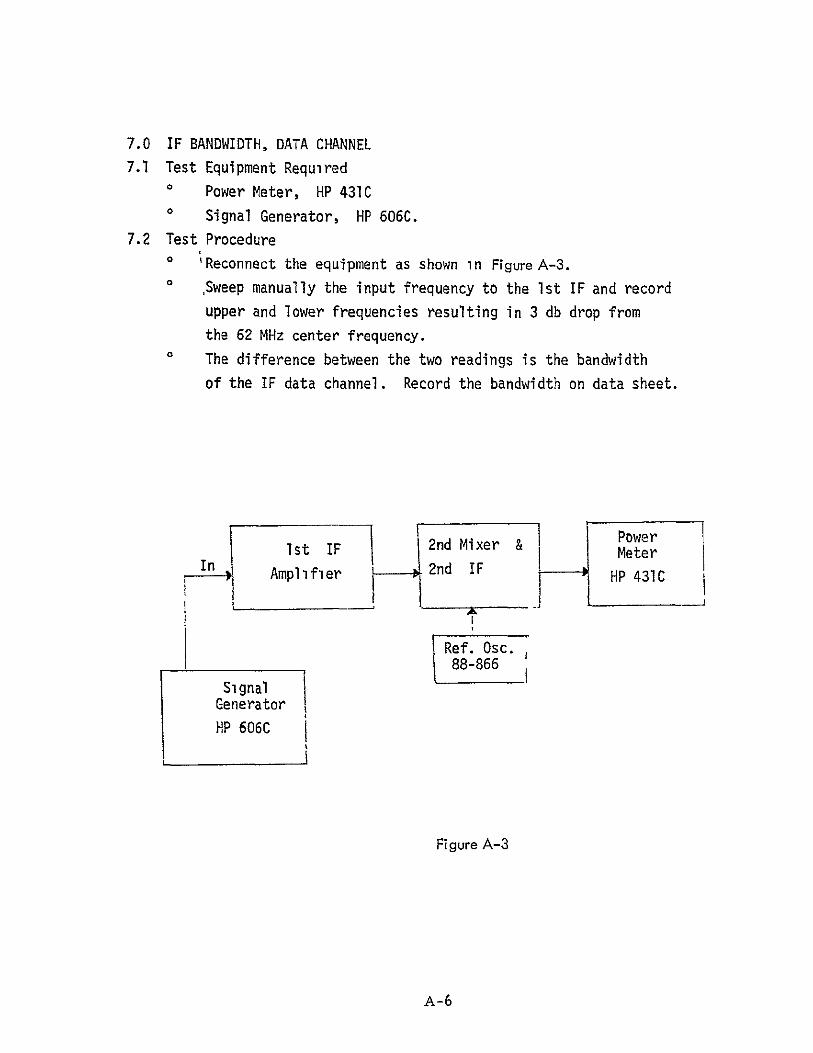