Embed Size (px)
Citation preview
Beyond 28nm: New Frontiers and Innovations in
Design For Manufacturability at the Limits of the
Scaling Roadmap
Luigi Capodieci, Ph.D.
DFM Director - R&D Fellow

Outline
2 Luigi Capodieci, Ph.D. - Director DFM
Challenges
Variability and the Limits of IC Geometrical Scaling
Methodology Innovation in Design for Manufacturing
Solutions
Advanced Rule-Based Verification (Yield Analysis and Yield Enhancement)
Novel Flow: DRC+ 2D Shapes Pattern-Matching Based Physical Design Verification
Model Accuracy and Full-Chip Performance without Compromise
Si-Accurate Model-Based Printability Verification: enabling special ‘tech-cell’ constructs
Manufacturing: closing the variability loop
Design-Enabled Manufacturing: Faster Yield Ramp and Foundry Customer Value

IC Integration State of the Art (today)
Scaling and Device Density
Gate First HKMG
28nm “Gate First” provides true
scaling (relative to 40nm)
1. ~100% density increase
2. Up to 50% increased speed and 50%
reduction in energy/switch
3. Sustains 40nm Layout Style Advantages:
Bi-directional Poly, Poly Jogs, Large
Caps
4. 10-20% Smaller Die Relative to 28nm
“Gate Last”
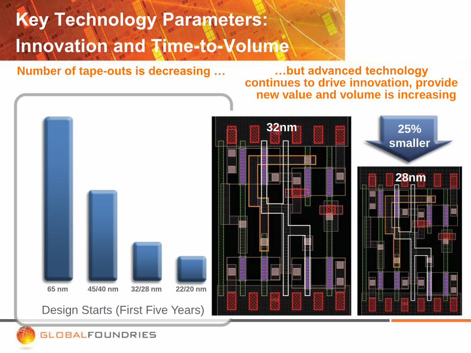
Process 90nm 65nm 40nm 28nm
Device Density 1 2 5 10
Normalized Power per gate 1 0.6 0.36 0.22
90nm
65nm
40nm
28nm
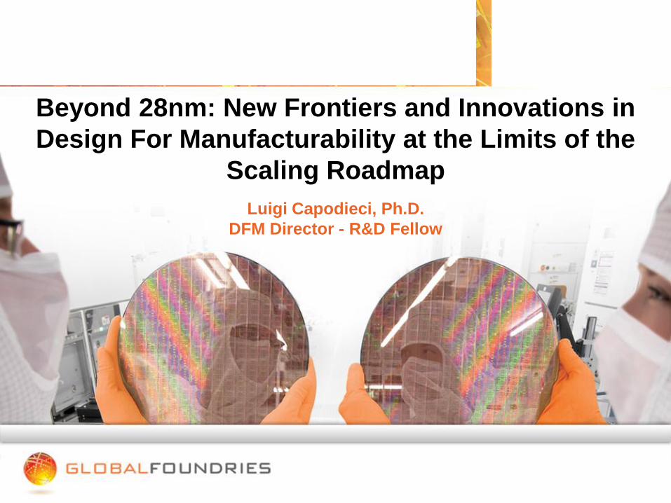
Key Technology Parameters:
Innovation and Time-to-Volume
Number of tape-outs is decreasing …
65 nm 45/40 nm 32/28 nm 22/20 nm
Design Starts (First Five Years)
…but advanced technology continues to drive innovation, provide
new value and volume is increasing
28nm
25%
smaller
32nm
5 Luigi Capodieci, Ph.D. - Director DFM
Process
Device Density
Normalized
Power per Gate
90nm
1
1
65nm
2
0.6
40nm
5
0.36
28nm
10
0.22
20nm
20
0.14
20nm: Scaling and Integration Continue

Disruptive Transition: New Integration
Schemes
From 28nm FEOL to 20nm MOL 28nm Below M1: - 2 vias - one PC, one RX Nxtgrd size: 19M Carac. Time: 35h
20nm Below M1: - 6 vias - 3 PC, 3 RX, CA, CB, TS Nxtgrd size: 147M Carac. Time: 150h
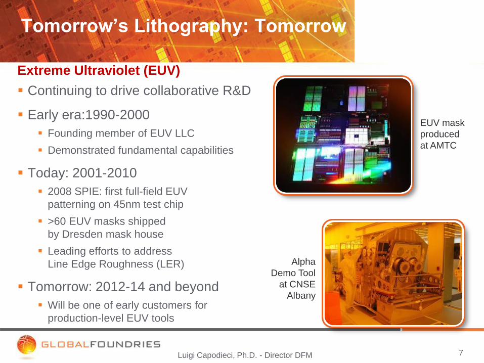
Tomorrow’s Lithography: Tomorrow
7 Luigi Capodieci, Ph.D. - Director DFM
Extreme Ultraviolet (EUV)
Continuing to drive collaborative R&D
Early era:1990-2000
Founding member of EUV LLC
Demonstrated fundamental capabilities
Today: 2001-2010
2008 SPIE: first full-field EUV
patterning on 45nm test chip
>60 EUV masks shipped
by Dresden mask house
Leading efforts to address
Line Edge Roughness (LER)
Tomorrow: 2012-14 and beyond
Will be one of early customers for
production-level EUV tools
EUV mask
produced
at AMTC
Alpha
Demo Tool
at CNSE
Albany
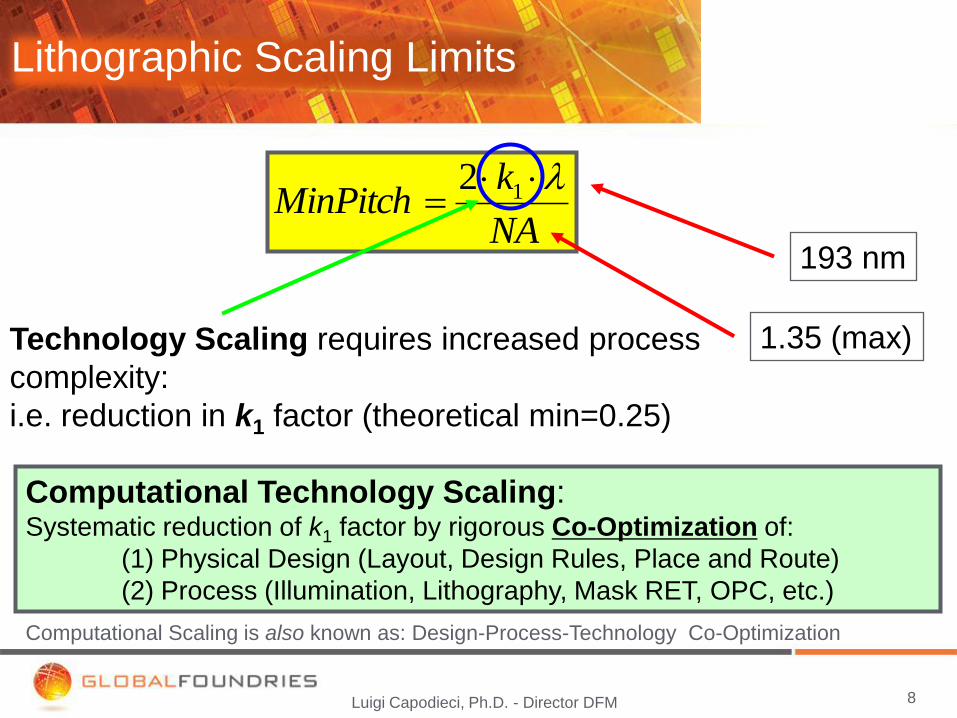
NA
kMinPitch
12
193 nm
1.35 (max) Technology Scaling requires increased process
complexity:
i.e. reduction in k1 factor (theoretical min=0.25)
Computational Technology Scaling: Systematic reduction of k1 factor by rigorous Co-Optimization of:
(1) Physical Design (Layout, Design Rules, Place and Route)
(2) Process (Illumination, Lithography, Mask RET, OPC, etc.)
Computational Scaling is also known as: Design-Process-Technology Co-Optimization
Lithographic Scaling Limits
8 Luigi Capodieci, Ph.D. - Director DFM
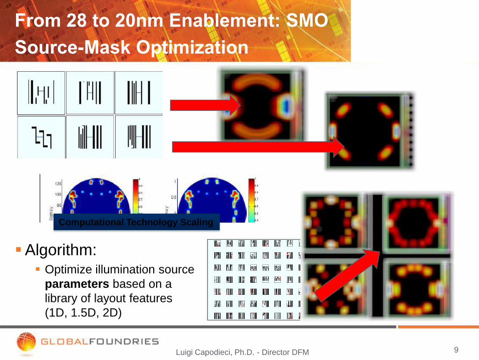
From 28 to 20nm Enablement: SMO
Source-Mask Optimization
9 Luigi Capodieci, Ph.D. - Director DFM
Algorithm: Optimize illumination source
parameters based on a
library of layout features
(1D, 1.5D, 2D)
Computational Technology Scaling
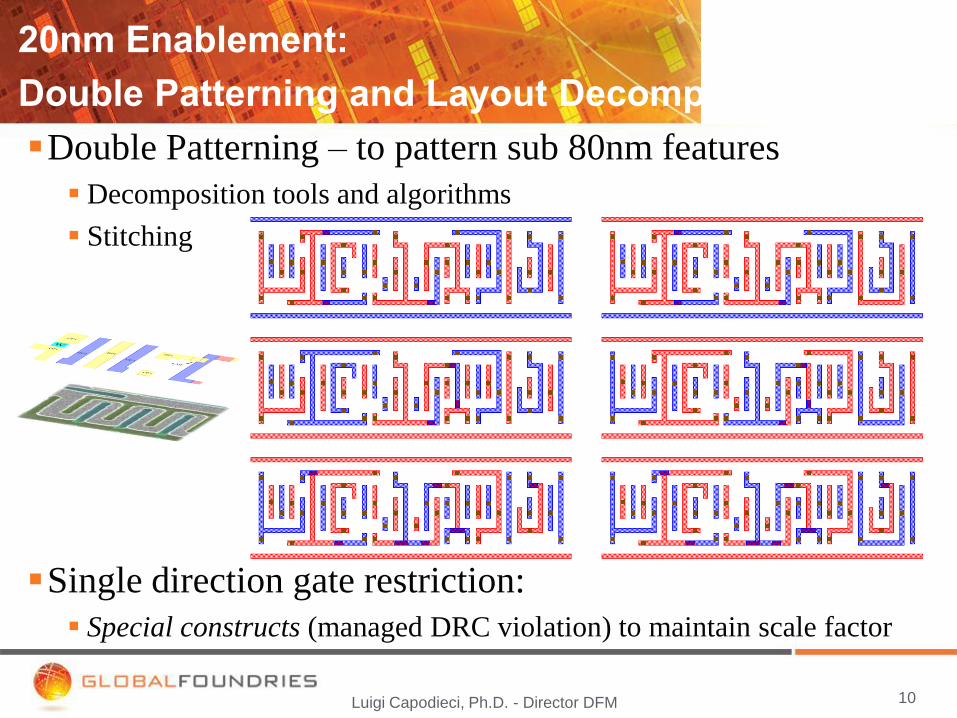
20nm Enablement:
Double Patterning and Layout Decomposition
10 Luigi Capodieci, Ph.D. - Director DFM
Double Patterning – to pattern sub 80nm features
Decomposition tools and algorithms
Stitching
Single direction gate restriction:
Special constructs (managed DRC violation) to maintain scale factor

Double patterning: Overlay
Implications
11 Luigi Capodieci, Ph.D. - Director DFM
CD 1
CD 2
CD2-CD1=2OL (3s)
22
2
2
12
1
2
1
)3(
OVCDUCDU
CDU
CDCD
s
Overlay can cause local line width variations or local space CD
variation depending on process scheme, which is translated into
electrical performance degradation: Gate with variation, gate length variation, resistance variation, capacitance variation
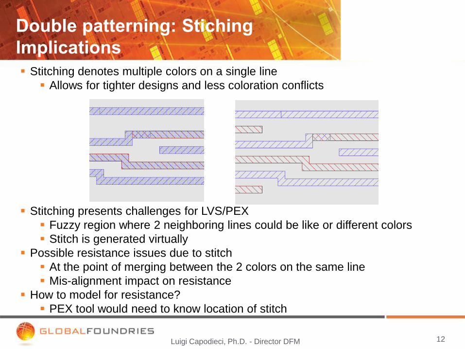
Double patterning: Stiching
Implications
12 Luigi Capodieci, Ph.D. - Director DFM
Stitching denotes multiple colors on a single line
Allows for tighter designs and less coloration conflicts
Stitching presents challenges for LVS/PEX
Fuzzy region where 2 neighboring lines could be like or different colors
Stitch is generated virtually
Possible resistance issues due to stitch
At the point of merging between the 2 colors on the same line
Mis-alignment impact on resistance
How to model for resistance?
PEX tool would need to know location of stitch
Retargeting (Physical Design)
13 Luigi Capodieci, Ph.D. - Director DFM
Retargeting denotes the operation of taking physical design shapes
provided by the designer and turning them into “target shapes”.
Motivation for retargeting functions in PEX
Decreased Complication For Designers
Improved Extraction run-time
Support of all input types, including GDS and LEF/DEF
Common PEX tech files for transistor and cell level extractions
Possible accuracy and simulation run-time improvements
Motivation for retargeting functions in LVS
Remove need for separate module
Eliminate issues caused by integrating separate module with LVS
No special license requirements
Managed Variability through DFM
14 Luigi Capodieci, Ph.D. - Director DFM
DFM brings manufacturing variability awareness into design
through EDA tools enablement
Advanced Rule-Based Verification (Yield Analysis/Scoring
and Automated Yield Enhancement)
Novel Flow: DRC+ 2D Shapes Pattern-Matching Based Physical Design Verification
Model Accuracy and Full-Chip Performance
Seamless Integration in P&R Flow
Si-Accurate Model-Based Printability Verification with
Applications to Special Constructs (tech-cells)
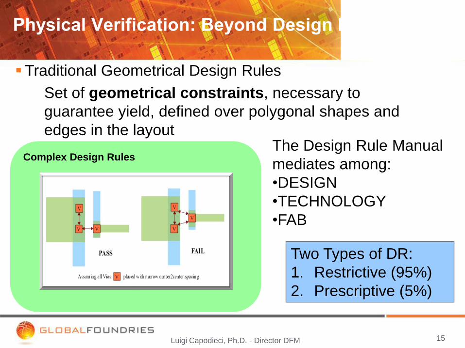
Physical Verification: Beyond Design Rules
15 Luigi Capodieci, Ph.D. - Director DFM
Traditional Geometrical Design Rules
Set of geometrical constraints, necessary to
guarantee yield, defined over polygonal shapes and
edges in the layout The Design Rule Manual
mediates among:
•DESIGN
•TECHNOLOGY
•FAB
Two Types of DR:
1. Restrictive (95%)
2. Prescriptive (5%)
Complex Design Rules

At 28nm and below:
Physical Design dependent Yield
16 Luigi Capodieci, Ph.D. - Director DFM
Feature-Feature Space
0%
0
100%
Yield
Yield Dependency for a given
Design Rule, for different layout
features: due to complex RET/OPC,
Optical/Process effects, etc.
allowed minimum space
Traditional
Design Rule
Ground Rules (binary) …
turn into DFM Rules (continuous)

DRC Clean
DRC Clean
Manufacturable
Process Window
Process Window - Yield Limiters
Model-Based Printability Verification
for DRC clean physical design
17
At 28nm, 20nm and below:
Si-Accurate Model-Based Verification is needed
Luigi Capodieci, Ph.D. - Director DFM
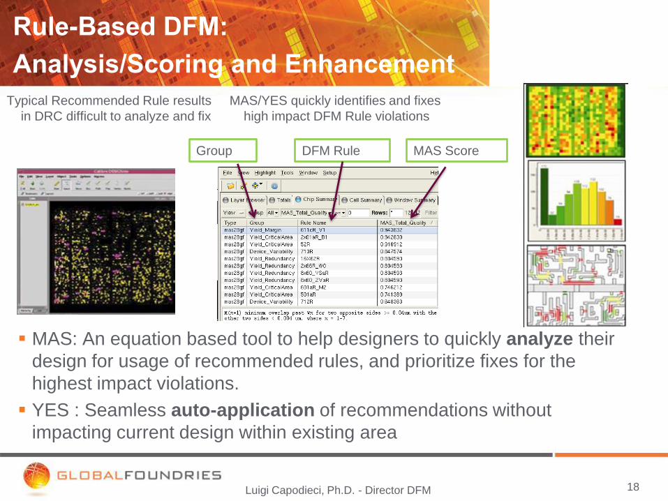
Rule-Based DFM:
Analysis/Scoring and Enhancement
18 Luigi Capodieci, Ph.D. - Director DFM
MAS: An equation based tool to help designers to quickly analyze their
design for usage of recommended rules, and prioritize fixes for the
highest impact violations.
YES : Seamless auto-application of recommendations without
impacting current design within existing area
Typical Recommended Rule results
in DRC difficult to analyze and fix
MAS/YES quickly identifies and fixes
high impact DFM Rule violations
Group MAS Score DFM Rule
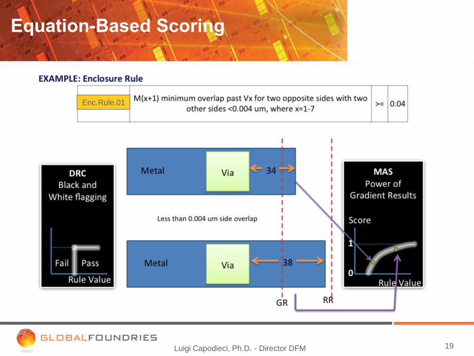
Equation-Based Scoring
19 Luigi Capodieci, Ph.D. - Director DFM
Enc.Rule.01
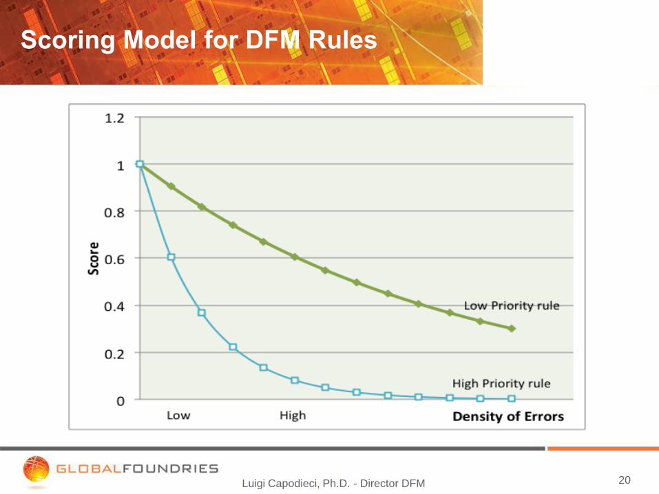
Scoring Model for DFM Rules
20 Luigi Capodieci, Ph.D. - Director DFM
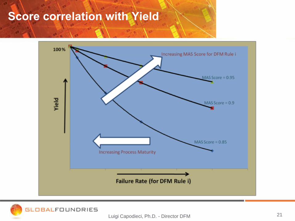
Score correlation with Yield
21 Luigi Capodieci, Ph.D. - Director DFM
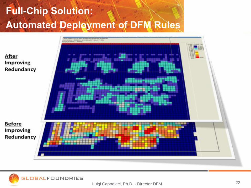
Full-Chip Solution:
Automated Deployment of DFM Rules
22 Luigi Capodieci, Ph.D. - Director DFM
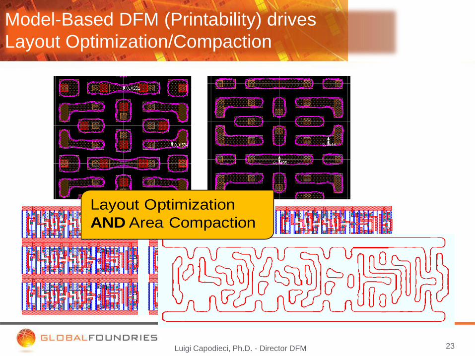
Layout Optimization
AND Area Compaction
23
Model-Based DFM (Printability) drives
Layout Optimization/Compaction
Luigi Capodieci, Ph.D. - Director DFM

24
DRC+: Based on 2D Shapes Pattern-Matching:
10,000X Faster than Simulation
Luigi Capodieci, Ph.D. - Director DFM
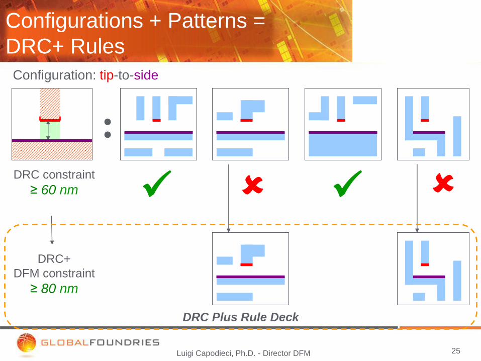
:
DRC constraint
≥ 60 nm
Configuration: tip-to-side
DRC+
DFM constraint
≥ 80 nm
DRC Plus Rule Deck
25
Configurations + Patterns =
DRC+ Rules
Luigi Capodieci, Ph.D. - Director DFM
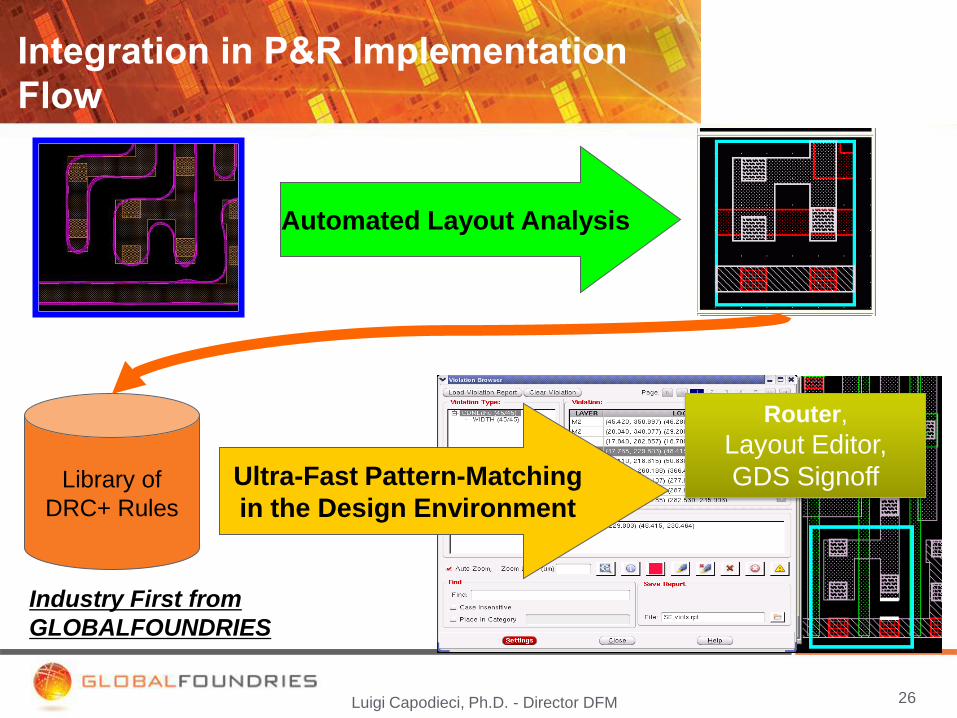
Integration in P&R Implementation
Flow
26 Luigi Capodieci, Ph.D. - Director DFM
Automated Layout Analysis
Library of
DRC+ Rules
Ultra-Fast Pattern-Matching
in the Design Environment
Router,
Layout Editor,
GDS Signoff
Industry First from
GLOBALFOUNDRIES
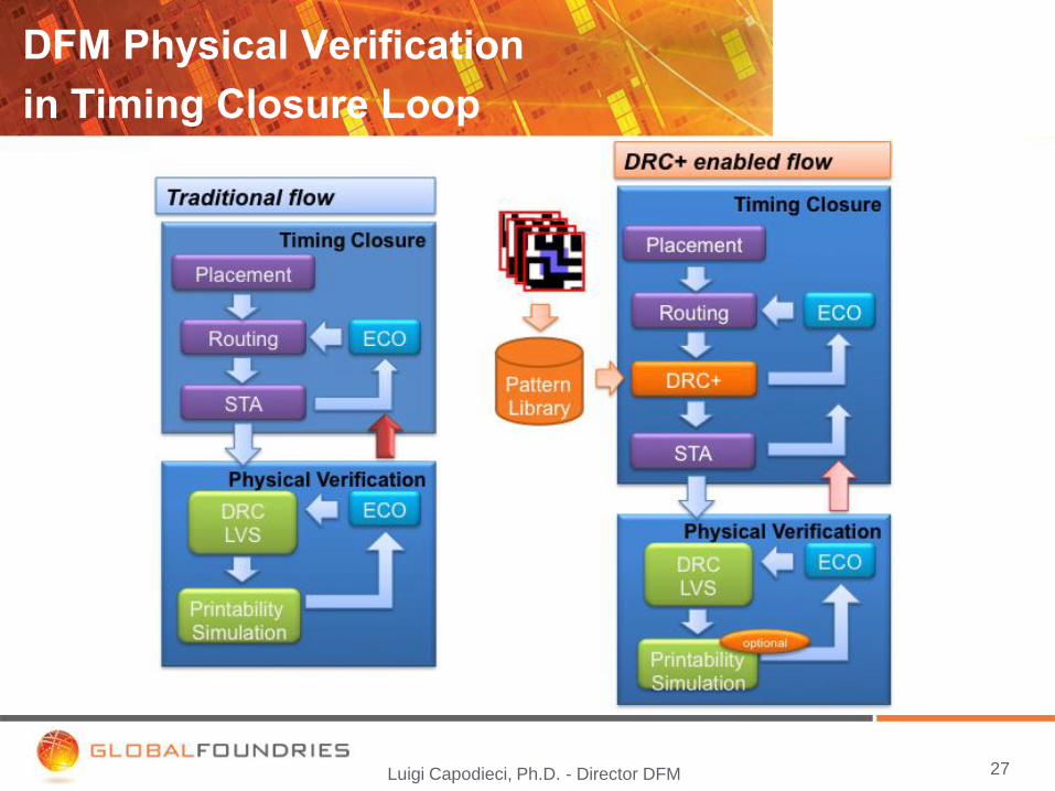
DFM Physical Verification
in Timing Closure Loop
27 Luigi Capodieci, Ph.D. - Director DFM
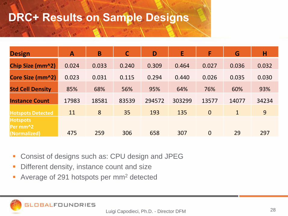
DRC+ Results on Sample Designs
28 Luigi Capodieci, Ph.D. - Director DFM
Design A B C D E F G H
Chip Size (mm^2) 0.024 0.033 0.240 0.309 0.464 0.027 0.036 0.032
Core Size (mm^2) 0.023 0.031 0.115 0.294 0.440 0.026 0.035 0.030
Std Cell Density 85% 68% 56% 95% 64% 76% 60% 93%
Instance Count 17983 18581 83539 294572 303299 13577 14077 34234
Consist of designs such as: CPU design and JPEG
Different density, instance count and size
Average of 291 hotspots per mm2 detected
Hotspots Detected 11 8 35 193 135 0 1 9 Hotspots Per mm^2 (Normalized) 475 259 306 658 307 0 29 297

Automated Fixing and Timing Closure
29 Luigi Capodieci, Ph.D. - Director DFM
100% of DRC+ hotspots auto fixing with 2 iterations
Timing delta after fix is significant enough to affect timing closure
Essential to include DFM physical verification & fixing in timing closure
Max Timing Delta (ps) 43 19 5 48 23 N/A 3 45
A B C D E F G H
Auto-Fix Iterations
Hotspots Found
1 11 8 35 193 135 0 1 9
2 0 0 0 1 0 - 0 0
3 - - - 0 - - - -
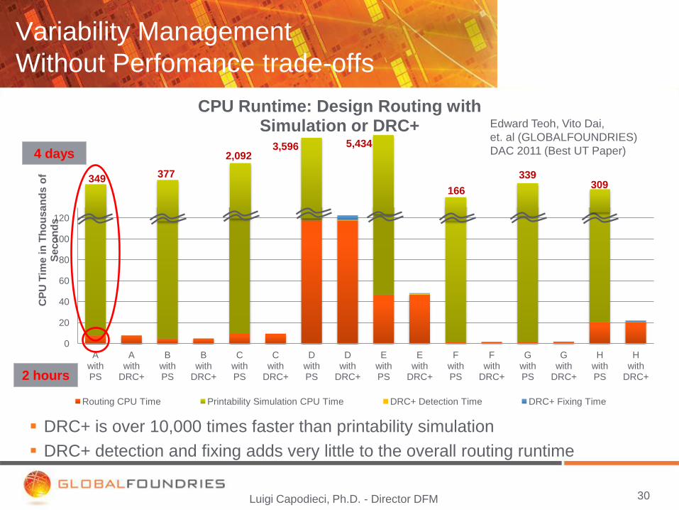
Variability Management
Without Perfomance trade-offs
DRC+ is over 10,000 times faster than printability simulation
DRC+ detection and fixing adds very little to the overall routing runtime
30
0
20
40
60
80
100
120
A with PS
A with
DRC+
B with PS
B with
DRC+
C with PS
C with
DRC+
D with PS
D with
DRC+
E with PS
E with
DRC+
F with PS
F with
DRC+
G with PS
G with
DRC+
H with PS
H with
DRC+
CP
U T
ime
in
Th
ou
sa
nd
s o
f S
eco
nd
s
CPU Runtime: Design Routing with Simulation or DRC+
Routing CPU Time Printability Simulation CPU Time DRC+ Detection Time DRC+ Fixing Time
309
3,596 5,434
349 377
2,092
166
339
2 hours
4 days
Edward Teoh, Vito Dai,
et. al (GLOBALFOUNDRIES)
DAC 2011 (Best UT Paper)
Luigi Capodieci, Ph.D. - Director DFM

130nm SRAM
Traditional layout
90nm SRAM
Uni-directional poly
45nm SRAM
Immersion, uniform poly CD
32nm SRAM
Double patterning
65nm SRAM
Uni-directional active
20nm SRAM
Higher NA immersion
Fine-tuned Design-Technology Co-Optimization:
Critical at 20nm!
31 Luigi Capodieci, Ph.D. - Director DFM
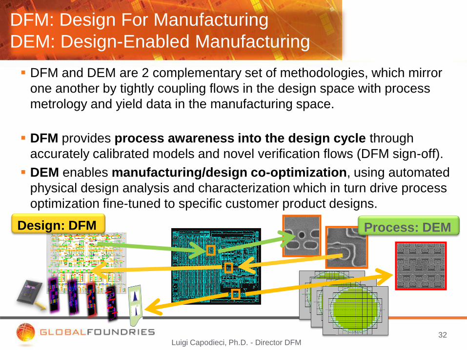
DFM and DEM are 2 complementary set of methodologies, which mirror
one another by tightly coupling flows in the design space with process
metrology and yield data in the manufacturing space.
DFM provides process awareness into the design cycle through
accurately calibrated models and novel verification flows (DFM sign-off).
DEM enables manufacturing/design co-optimization, using automated
physical design analysis and characterization which in turn drive process
optimization fine-tuned to specific customer product designs.
Process: DEM
32
DFM: Design For Manufacturing
DEM: Design-Enabled Manufacturing
Design: DFM
Luigi Capodieci, Ph.D. - Director DFM

Pattern-Matching supports
Design-Enabled-Manufacturing
33 Luigi Capodieci, Ph.D. - Director DFM
I=226; M=89%
I=226; M=89%
I=52; M=83%
Binary Bitmap
from SEM Image Full-Chip
Pattern-Match
(X,Y) Locations
I=84; M=94%
Match
Results:
Exact
and Fuzzy
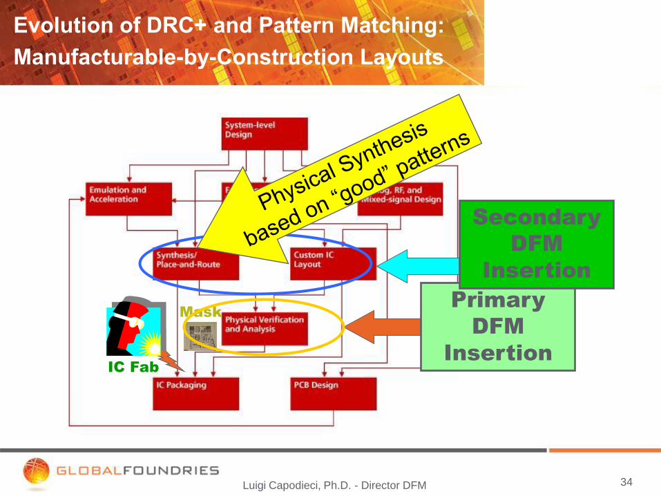
Evolution of DRC+ and Pattern Matching:
Manufacturable-by-Construction Layouts
IC Fab
Mask
Primary
DFM
Insertion
Secondary
DFM
Insertion
Luigi Capodieci, Ph.D. - Director DFM 34
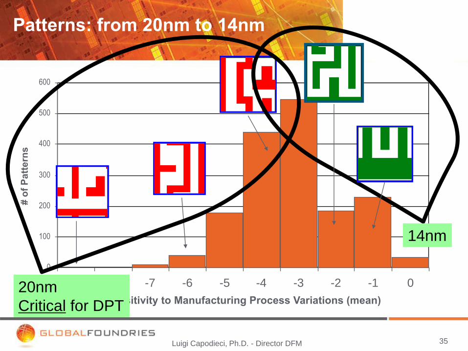
Patterns: from 20nm to 14nm
35 Luigi Capodieci, Ph.D. - Director DFM
0
100
200
300
400
500
600
-9 -8 -7 -6 -5 -4 -3 -2 -1 0
Sensitivity to Manufacturing Process Variations (mean)
# o
f P
att
ern
s
20nm
Critical for DPT
14nm
Design/Technology
Co-Optimization
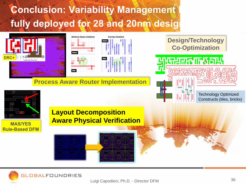
36 Luigi Capodieci, Ph.D. - Director DFM
Layout Decomposition
Aware Physical Verification
Technology Optimized
Constructs (tiles, bricks)
Process Aware Router Implementation
Conclusion: Variability Management Flows
fully deployed for 28 and 20nm designs
Page 37