Embed Size (px)
Citation preview
TIBPAL16L8-7C, TIBPAL16R4-7C, TIBPAL16R6-7C, TIBPAL16R8-7CTIBPAL16L8-10M, TIBPAL16R4-10M, TIBPAL16R6-10M, TIBPAL16R8-10M
HIGH-PERFORMANCE IMPACT-X�™ PAL® CIRCUITSSRPS006E − D3115, MAY 1988 − REVISED DECEMBER 2010
POST OFFICE BOX 655303 • DALLAS, TEXAS 75265
Copyright © 2010, Texas Instruments Incorporated
1
PRODUCTION DATA information is current as of publication date.Products conform to specifications per the terms of Texas Instrumentsstandard warranty. Production processing does not necessarily includetesting of all parameters.
• High-Performance Operation:fmax (no feedback)
TIBPAL16R’-7C Series . . . 100 MHz MinTIBPAL16R’-10M Series . . . 62.5 MHz Min
fmax (internal feedback)TIBPAL16R’-7C Series . . . 100 MHz MinTIBPAL16R’-10M Series . . . 62.5 MHz Min
fmax (external feedback)TIBPAL16R’-7C Series . . . 74 MHz MinTIBPAL16R’-10M Series . . . 52.5 MHz Min
Propagation DelayTIBPAL16L’-7C Series . . . 7 ns MaxTIBPAL16L’-10M Series . . . 10 ns Max
• Functionally Equivalent, but Faster than,Existing 20-Pin PLDs
• Preload Capability on Output RegistersSimplifies Testing
• Power-Up Clear on Registered Devices (AllRegister Outputs are Set Low, but VoltageLevels at the Output Pins Go High)
• Package Options Include Both Plastic andCeramic Chip Carriers in Addition to Plasticand Ceramic DIPs
• Security Fuse Prevents Duplication
• Dependable Texas Instruments Quality andReliability
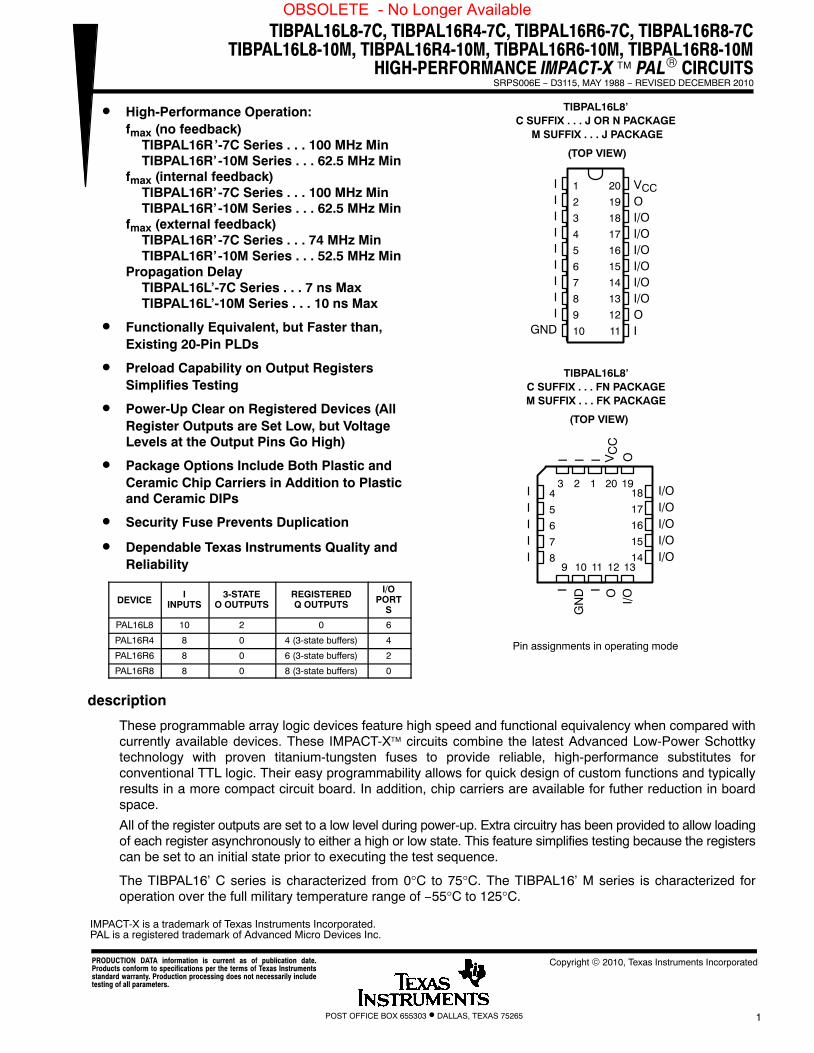
DEVICEI
INPUTS3-STATE
O OUTPUTSREGISTEREDQ OUTPUTS
I/OPORT
S
PAL16L8 10 2 0 6
PAL16R4 8 0 4 (3-state buffers) 4
PAL16R6 8 0 6 (3-state buffers) 2
PAL16R8 8 0 8 (3-state buffers) 0
description
These programmable array logic devices feature high speed and functional equivalency when compared withcurrently available devices. These IMPACT-X™ circuits combine the latest Advanced Low-Power Schottkytechnology with proven titanium-tungsten fuses to provide reliable, high-performance substitutes forconventional TTL logic. Their easy programmability allows for quick design of custom functions and typicallyresults in a more compact circuit board. In addition, chip carriers are available for futher reduction in boardspace.
All of the register outputs are set to a low level during power-up. Extra circuitry has been provided to allow loadingof each register asynchronously to either a high or low state. This feature simplifies testing because the registerscan be set to an initial state prior to executing the test sequence.
The TIBPAL16’ C series is characterized from 0°C to 75°C. The TIBPAL16’ M series is characterized foroperation over the full military temperature range of −55°C to 125°C.
IMPACT-X is a trademark of Texas Instruments Incorporated.PAL is a registered trademark of Advanced Micro Devices Inc.
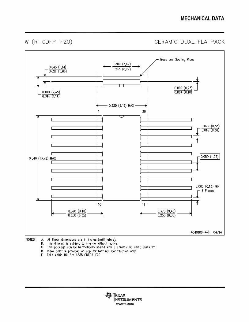
Pin assignments in operating mode
1
2
3
4
5
6
7
8
9
10
20
19
18
17
16
15
14
13
12
11
IIIIIIIII
GND
VCCOI/OI/OI/OI/OI/OI/OOI
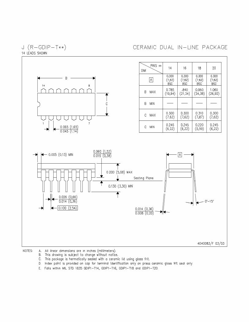
TIBPAL16L8’C SUFFIX . . . J OR N PACKAGE
M SUFFIX . . . J PACKAGE
(TOP VIEW)
3 2 1 20 19
9 10 11 12 13
4
5
6
7
8
18
17
16
15
14
I/OI/OI/OI/OI/O
IIIII
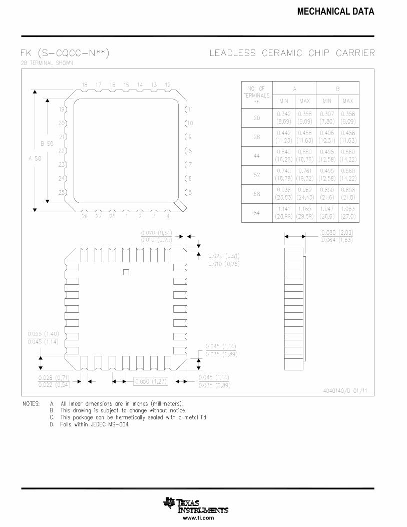
TIBPAL16L8’C SUFFIX . . . FN PACKAGEM SUFFIX . . . FK PACKAGE
(TOP VIEW)
I I IO I/O
O
IG
ND I
VC
C
OBSOLETE - No Longer Available
TIBPAL16R4-7C, TIBPAL16R6-7C, TIBPAL16R8-7CTIBPAL16R4-10M, TIBPAL16R6-10M, TIBPAL16R8-10MHIGH-PERFORMANCE IMPACT-X�™ PAL® CIRCUITSSRPS006E − D3115, MAY 1988 − REVISED DECEMBER 2010
POST OFFICE BOX 655303 • DALLAS, TEXAS 752652
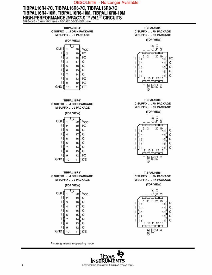
Pin assignments in operating mode
1
2
3
4
5
6
7
8
9
10
20
19
18
17
16
15
14
13
12
11
CLKIIIIIIII
GND
VCCI/OI/OQQQQI/OI/OOE
(TOP VIEW)
TIBPAL16R4’C SUFFIX . . . J OR N PACKAGE
M SUFFIX . . . J PACKAGE
1
2
3
4
5
6
7
8
9
10
20
19
18
17
16
15
14
13
12
11
CLKIIIIIIII
GND
VCCI/OQQQQQQI/OOE
(TOP VIEW)
TIBPAL16R6’C SUFFIX . . . J OR N PACKAGE
M SUFFIX . . . J PACKAGE
1
2
3
4
5
6
7
8
9
10
20
19
18
17
16
15
14
13
12
11
CLKIIIIIIII
GND
VCCQQQQQQQQOE
(TOP VIEW)
TIBPAL16R8’C SUFFIX . . . J OR N PACKAGE
M SUFFIX . . . J PACKAGE
I I CLK
I/O I/OI/O
IG
ND
VC
CO
E
3 2 1 20 19
9 10 11 12 13
4
5
6
7
8
18
17
16
15
14
I/OQQQQ
IIIII
(TOP VIEW)
TIBPAL16R4’C SUFFIX . . . FN PACKAGEM SUFFIX . . . FK PACKAGE
I I CLK
I/O QI/O
IG
ND
VC
C
3 2 1 20 19
9 10 11 12 13
4
5
6
7
8
18
17
16
15
14
QQQQQ
IIIII
(TOP VIEW)
OE
TIBPAL16R6’C SUFFIX . . . FN PACKAGEM SUFFIX . . . FK PACKAGE
I I CLK
Q QQ
IG
ND
VC
CO
E
3 2 1 20 19
9 10 11 12 13
4
5
6
7
8
18
17
16
15
14
QQQQQ
IIIII
(TOP VIEW)
TIBPAL16R8’C SUFFIX . . . FN PACKAGEM SUFFIX . . . FK PACKAGE
OBSOLETE - No Longer Available
TIBPAL16L8-7C, TIBPAL16R4-7CTIBPAL16L8-10M, TIBPAL16R4-10M
HIGH-PERFORMANCE IMPACT-X�™ PAL® CIRCUITSSRPS006E − D3115, MAY 1988 − REVISED DECEMBER 2010
POST OFFICE BOX 655303 • DALLAS, TEXAS 75265 3
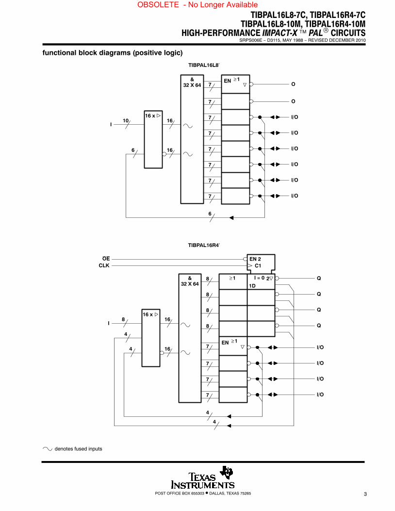
functional block diagrams (positive logic)
denotes fused inputs
TIBPAL16L8’
TIBPAL16R4’
O
O
I/O
I/O
I/O
I/O
I/O
I/O
I
EN ≥1&32 X 64
10 16
166
7
7
7
7
7
7
7
7
6
16 x
Q
I/O
I/O
I/O
I/O
I
EN
8 16
164
7
7
7
8
8
8
7
4
16 x
≥1
&32 X 64
≥1
8
Q
Q
Q
4
1D
I = 0 2
CLK C1EN 2OE
4
OBSOLETE - No Longer Available
TIBPAL16R6-7C, TIBPAL16R8-7CTIBPAL16R6-10M, TIBPAL16R8-10MHIGH-PERFORMANCE IMPACT-X�™ PAL® CIRCUITSSRPS006E − D3115, MAY 1988 − REVISED DECEMBER 2010
POST OFFICE BOX 655303 • DALLAS, TEXAS 752654
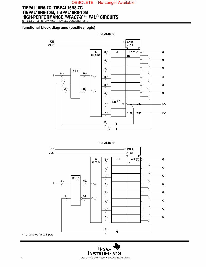
functional block diagrams (positive logic)
denotes fused inputs
TIBPAL16R6’
TIBPAL16R8’
Q
I/O
I/O
I
EN
8 16
162
7
8
8
8
7
2
16 x
≥1
&32 X 64
≥1
8
Q
Q
Q
6
1D
I = 0 2
CLK C1EN 2OE
6
8 Q
8 Q
Q
I8 16
168
8
8
8
8
16 x
8
Q
Q
Q
1D
I = 0 2
CLK C1EN 2
8 Q
8 Q
&32 X 64
≥1
OE
8 Q
8 Q
OBSOLETE - No Longer Available
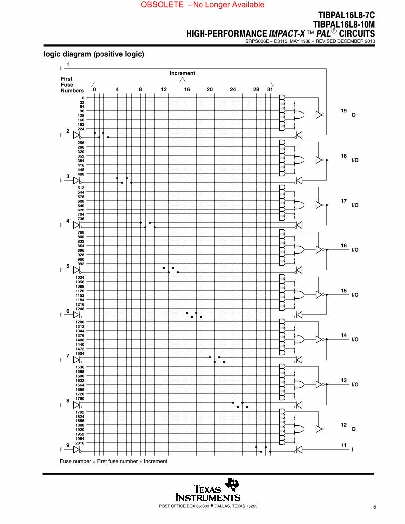
0 4 8 12 16 20 24 28 31
I2
I3
I4
I5
I6
I7
I8
I9
O19
I/O18
I/O17
I/O16
I/O15
I/O14
I/O13
O12
I11
IncrementI
1
Fuse number = First fuse number + Increment
0326496
128160192224
256288320352384416448480
512544576608640672704736
768800832864896928960992
10241056108811201152118412161248
12801312134413761408144014721504
15361568160016321664169617281760
17921824185618881920195219842016
FirstFuseNumbers
TIBPAL16L8-7CTIBPAL16L8-10M
HIGH-PERFORMANCE IMPACT-X�™ PAL® CIRCUITSSRPS006E − D3115, MAY 1988 − REVISED DECEMBER 2010
POST OFFICE BOX 655303 • DALLAS, TEXAS 75265 5
logic diagram (positive logic)
OBSOLETE - No Longer Available
0 4 8 12 16 20 24 28 31
I2
I3
I4
I5
I6
I7
I8
I9
I/O19
I/O18
Q17
Q16
Q15
Q14
I/O13
I/O12
11
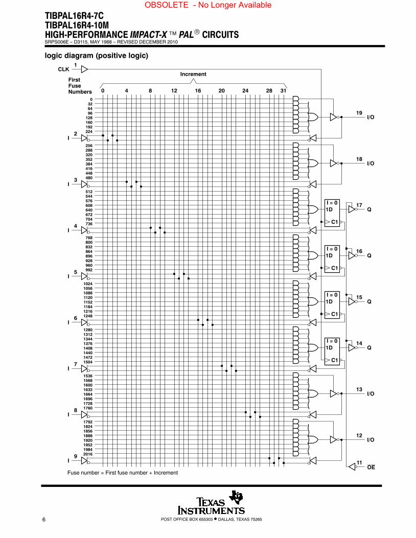
IncrementCLK
1
Fuse number = First fuse number + Increment
0326496
128160192224
256288320352384416448480
512544576608640672704736
768800832864896928960992
10241056108811201152118412161248
12801312134413761408144014721504
15361568160016321664169617281760
17921824185618881920195219842016
FirstFuseNumbers
C1
1DI = 0
C1
1DI = 0
C1
1DI = 0
C1
1DI = 0
OE
TIBPAL16R4-7CTIBPAL16R4-10MHIGH-PERFORMANCE IMPACT-X�™ PAL® CIRCUITSSRPS006E − D3115, MAY 1988 − REVISED DECEMBER 2010
POST OFFICE BOX 655303 • DALLAS, TEXAS 752656
logic diagram (positive logic)
OBSOLETE - No Longer Available
0 4 8 12 16 20 24 28 31
I2
I3
I4
I5
I6
I7
I8
I9
I/O19
Q17
Q16
Q15
Q14
I/O12
11
IncrementCLK
1
Fuse number = First fuse number + Increment
0326496
128160192224
256288320352384416448480
512544576608640672704736
768800832864896928960992
10241056108811201152118412161248
12801312134413761408144014721504
15361568160016321664169617281760
17921824185618881920195219842016
FirstFuseNumbers
C1
1DI = 0
C1
1DI = 0
C1
1DI = 0
C1
1DI = 0
OE
Q18
C1
1DI = 0
Q13
C1
1DI = 0
TIBPAL16R6-7CTIBPAL16R6-10M
HIGH-PERFORMANCE IMPACT-X�™ PAL® CIRCUITSSRPS006E − D3115, MAY 1988 − REVISED DECEMBER 2010
POST OFFICE BOX 655303 • DALLAS, TEXAS 75265 7
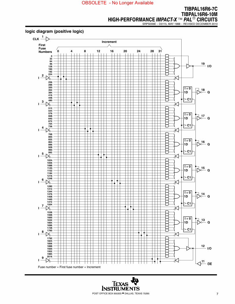
logic diagram (positive logic)
OBSOLETE - No Longer Available
0 4 8 12 16 20 24 28 31
I2
I3
I4
I5
I6
I7
I8
I9
Q17
Q16
Q15
Q14
11
IncrementCLK
1
Fuse number = First fuse number + Increment
0326496
128160192224
256288320352384416448480
512544576608640672704736
768800832864896928960992
10241056108811201152118412161248
12801312134413761408144014721504
15361568160016321664169617281760
17921824185618881920195219842016
FirstFuseNumbers
C1
1DI = 0
C1
1DI = 0
C1
1DI = 0
C1
1DI = 0
OE
Q18
C1
1DI = 0
Q13
C1
1DI = 0
Q19
C1
1DI = 0
Q12
C1
1DI = 0
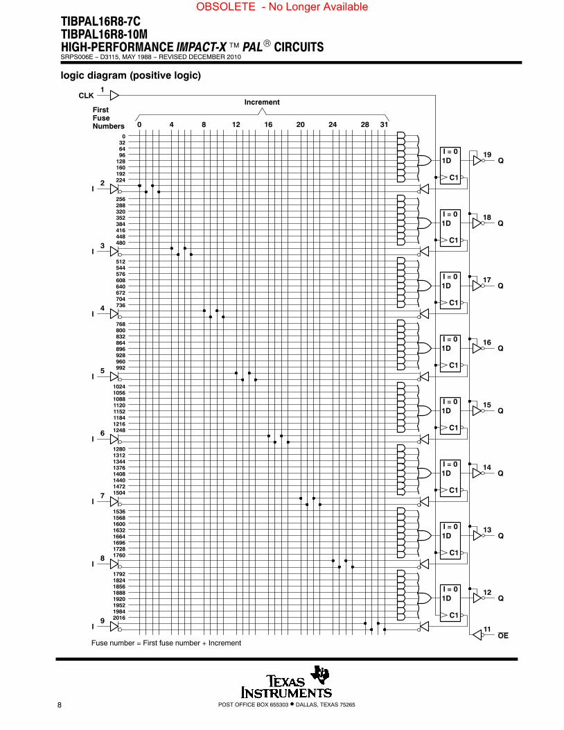
TIBPAL16R8-7CTIBPAL16R8-10MHIGH-PERFORMANCE IMPACT-X�™ PAL® CIRCUITSSRPS006E − D3115, MAY 1988 − REVISED DECEMBER 2010
POST OFFICE BOX 655303 • DALLAS, TEXAS 752658
logic diagram (positive logic)
OBSOLETE - No Longer Available
TIBPAL16L8-7C, TIBPAL16R4-7C, TIBPAL16R6-7C, TIBPAL16R8-7CHIGH-PERFORMANCE IMPACT-X�™ PAL® CIRCUITS
SRPS006E − D3115, MAY 1988 − REVISED DECEMBER 2010
POST OFFICE BOX 655303 • DALLAS, TEXAS 75265 9
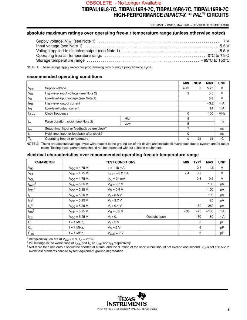
absolute maximum ratings over operating free-air temperature range (unless otherwise noted)
Supply voltage, VCC (see Note 1) 7 V. . . . . . . . . . . . . . . . . . . . . . . . . . . . . . . . . . . . . . . . . . . . . . . . . . . . . . . . . . . . Input voltage (see Note 1) 5.5 V. . . . . . . . . . . . . . . . . . . . . . . . . . . . . . . . . . . . . . . . . . . . . . . . . . . . . . . . . . . . . . . . . . Voltage applied to disabled output (see Note 1) 5.5 V. . . . . . . . . . . . . . . . . . . . . . . . . . . . . . . . . . . . . . . . . . . . . . . Operating free-air temperature range 0°C to 75°C. . . . . . . . . . . . . . . . . . . . . . . . . . . . . . . . . . . . . . . . . . . . . . . . . . Storage temperature range −65°C to 150°C. . . . . . . . . . . . . . . . . . . . . . . . . . . . . . . . . . . . . . . . . . . . . . . . . . . . . . . .
NOTE 1: These ratings apply except for programming pins during a programming cycle.
recommended operating conditionsMIN NOM MAX UNIT
VCC Supply voltage 4.75 5 5.25 V
VIH High-level input voltage (see Note 2) 2 5.5 V
VIL Low-level input voltage (see Note 2) 0.8 V
IOH High-level output current −3.2 mA
IOL Low-level output current 24 mA
fclock Clock frequency 0 100 MHz
High 5
Low 5
tsu Setup time, input or feedback before clock↑ 7 ns
th Hold time, input or feedback after clock↑ 0 ns
TA Operating free-air temperature 0 25 75 °CNOTE 2: These are absolute voltage levels with respect to the ground pin of the device and include all overshoots due to system and/or tester
noise. Testing these parameters should not be attempted without suitable equipment.
electrical characteristics over recommended operating free-air temperature range
PARAMETER TEST CONDITIONS MIN TYP† MAX UNIT
VIK VCC = 4.75 V, II = −18 mA −0.8 −1.5 V
VOH VCC = 4.75 V, IOH = −3.2 mA 2.4 3.2 V
VOL VCC = 4.75 V, IOL = 24 mA 0.3 0.5 V
IOZH‡ VCC = 5.25 V, VO = 2.7 V 100 μA
IOZL‡ VCC = 5.25 V, VO = 0.4 V −100 μA
II VCC = 5.25 V, VI = 5.5 V 100 μA
IIH‡ VCC = 5.25 V, VI = 2.7 V 25 μA
IIL‡ VCC = 5.25 V, VI = 0.4 V −80 −250 μA
IOS§ VCC = 5.25 V, VO = 0.5 V −30 −70 −130 mA
ICC VCC = 5.25 V, VI = 0, Outputs open 160 180 mA
Ci f = 1 MHz, VI = 2 V 5 pF
Co f = 1 MHz, VO = 2 V 6 pF
Cclk f = 1 MHz, VCLK = 2 V 6 pF
† All typical values are at VCC = 5 V, TA = 25°C.‡ I/O leakage is the worst case of IOZL and IIL or IOZH and IIH respectively.§ Not more than one output should be shorted at a time, and the duration of the short circuit should not exceed one second. VO is set at 0.5 V to
avoid test problems caused by test equipment ground degradation.
nsPulse duration, clock (see Note 2)tw
OBSOLETE - No Longer Available
I, I/O O, I/Otpd ns
TIBPAL16L8-7C, TIBPAL16R4-7C, TIBPAL16R6-7C, TIBPAL16R8-7CHIGH-PERFORMANCE IMPACT-X�™ PAL® CIRCUITS
SRPS006E − D3115, MAY 1988 − REVISED DECEMBER 2010
POST OFFICE BOX 655303 • DALLAS, TEXAS 7526510
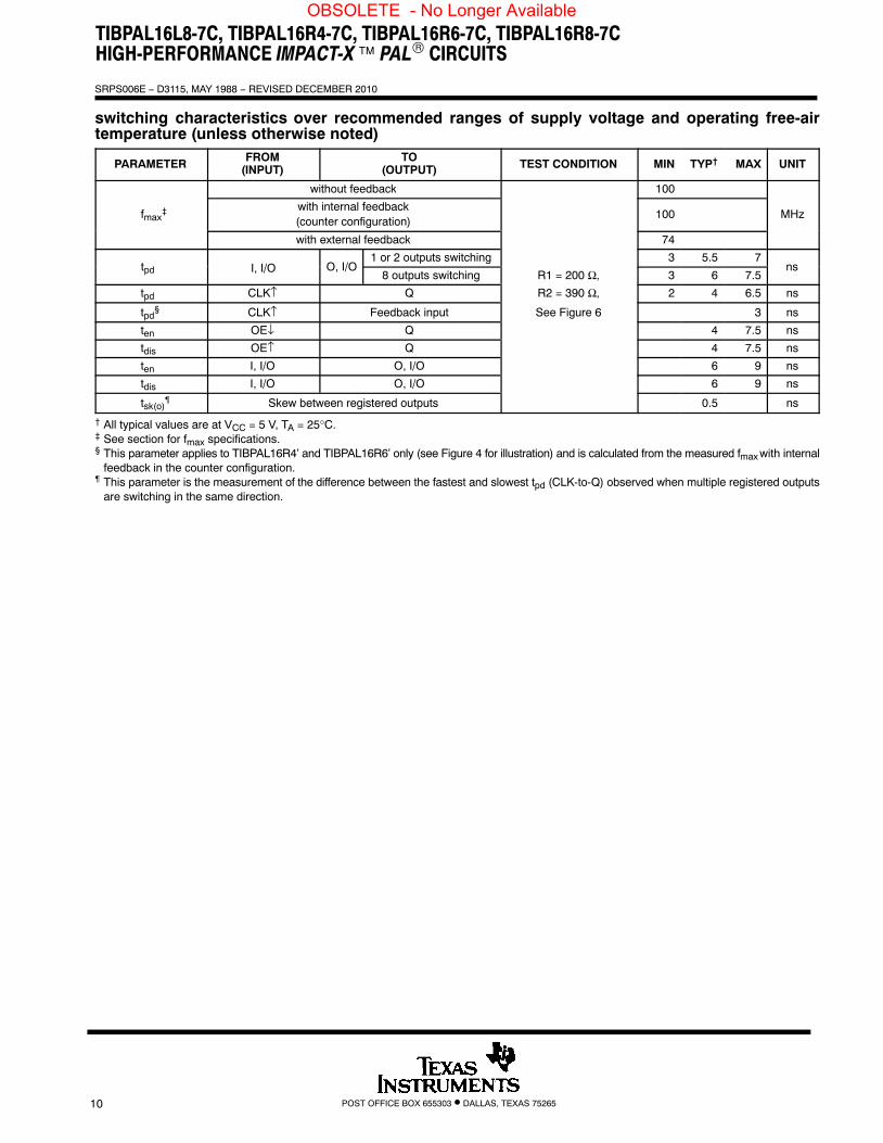
switching characteristics over recommended ranges of supply voltage and operating free-airtemperature (unless otherwise noted)
PARAMETERFROM
(INPUT)TO
(OUTPUT) TEST CONDITION MIN TYP† MAX UNIT
without feedback 100
fmax‡ with internal feedback
(counter configuration)100 MHz
with external feedback 74
1 or 2 outputs switching 3 5.5 7
8 outputs switching R1 = 200 Ω, 3 6 7.5
tpd CLK↑ Q R2 = 390 Ω, 2 4 6.5 ns
tpd§ CLK↑ Feedback input See Figure 6 3 ns
ten OE↓ Q 4 7.5 ns
tdis OE↑ Q 4 7.5 ns
ten I, I/O O, I/O 6 9 ns
tdis I, I/O O, I/O 6 9 ns
tsk(o)¶ Skew between registered outputs 0.5 ns
† All typical values are at VCC = 5 V, TA = 25°C.‡ See section for fmax specifications.§ This parameter applies to TIBPAL16R4’ and TIBPAL16R6’ only (see Figure 4 for illustration) and is calculated from the measured fmax with internal
feedback in the counter configuration.¶ This parameter is the measurement of the difference between the fastest and slowest tpd (CLK-to-Q) observed when multiple registered outputs
are switching in the same direction.
OBSOLETE - No Longer Available
μAVI = 2.7 V
VO = 0.4 V
VCC = 5.5 V,IIH
IOZL‡ VCC = 5.5 V, mA
TIBPAL16L8-10M, TIBPAL16R4-10M, TIBPAL16R6-10M, TIBPAL16R8-10MHIGH-PERFORMANCE IMPACT-X�™ PAL® CIRCUITS
SRPS006E − D3115, MAY 1988 − REVISED DECEMBER 2010
POST OFFICE BOX 655303 • DALLAS, TEXAS 75265 11
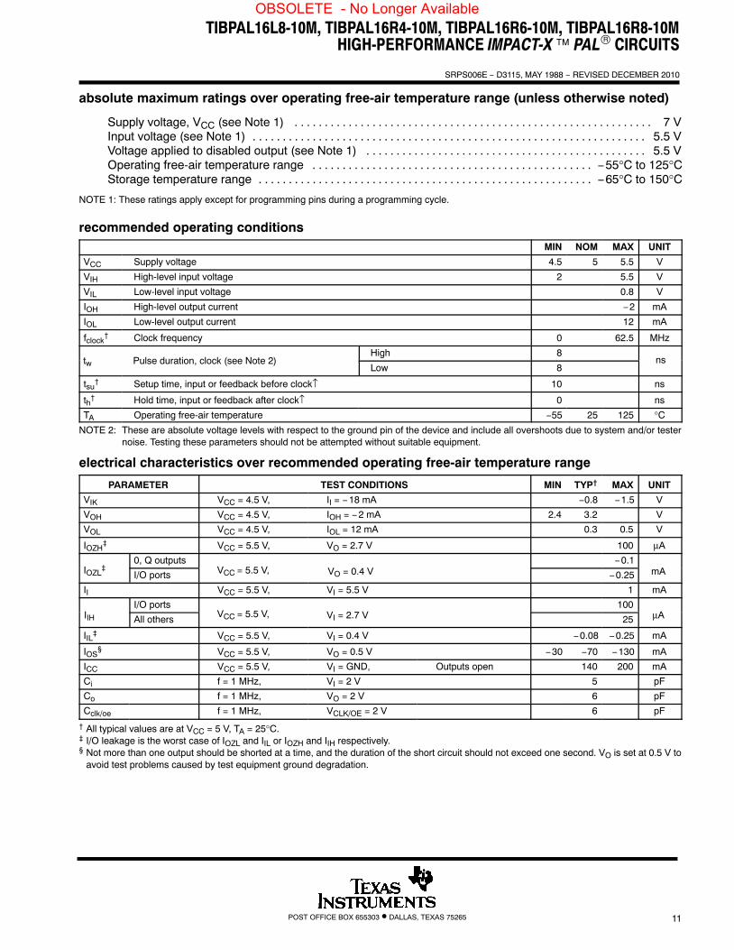
absolute maximum ratings over operating free-air temperature range (unless otherwise noted)
Supply voltage, VCC (see Note 1) 7 V. . . . . . . . . . . . . . . . . . . . . . . . . . . . . . . . . . . . . . . . . . . . . . . . . . . . . . . . . . . . Input voltage (see Note 1) 5.5 V. . . . . . . . . . . . . . . . . . . . . . . . . . . . . . . . . . . . . . . . . . . . . . . . . . . . . . . . . . . . . . . . . . Voltage applied to disabled output (see Note 1) 5.5 V. . . . . . . . . . . . . . . . . . . . . . . . . . . . . . . . . . . . . . . . . . . . . . . Operating free-air temperature range −55°C to 125°C. . . . . . . . . . . . . . . . . . . . . . . . . . . . . . . . . . . . . . . . . . . . . . . Storage temperature range −65°C to 150°C. . . . . . . . . . . . . . . . . . . . . . . . . . . . . . . . . . . . . . . . . . . . . . . . . . . . . . . .
NOTE 1: These ratings apply except for programming pins during a programming cycle.
recommended operating conditionsMIN NOM MAX UNIT
VCC Supply voltage 4.5 5 5.5 V
VIH High-level input voltage 2 5.5 V
VIL Low-level input voltage 0.8 V
IOH High-level output current −2 mA
IOL Low-level output current 12 mA
fclock† Clock frequency 0 62.5 MHz
High 8
Low 8
tsu† Setup time, input or feedback before clock↑ 10 ns
th† Hold time, input or feedback after clock↑ 0 ns
TA Operating free-air temperature −55 25 125 °CNOTE 2: These are absolute voltage levels with respect to the ground pin of the device and include all overshoots due to system and/or tester
noise. Testing these parameters should not be attempted without suitable equipment.
electrical characteristics over recommended operating free-air temperature range
PARAMETER TEST CONDITIONS MIN TYP† MAX UNIT
VIK VCC = 4.5 V, II = −18 mA −0.8 −1.5 V
VOH VCC = 4.5 V, IOH = −2 mA 2.4 3.2 V
VOL VCC = 4.5 V, IOL = 12 mA 0.3 0.5 V
IOZH‡ VCC = 5.5 V, VO = 2.7 V 100 μA
0, Q outputs −0.1
I/O ports −0.25
II VCC = 5.5 V, VI = 5.5 V 1 mA
I/O ports 100
All others 25
IIL‡ VCC = 5.5 V, VI = 0.4 V −0.08 −0.25 mA
IOS§ VCC = 5.5 V, VO = 0.5 V −30 −70 −130 mA
ICC VCC = 5.5 V, VI = GND, Outputs open 140 200 mA
Ci f = 1 MHz, VI = 2 V 5 pF
Co f = 1 MHz, VO = 2 V 6 pF
Cclk/oe f = 1 MHz, VCLK/OE = 2 V 6 pF
† All typical values are at VCC = 5 V, TA = 25°C.‡ I/O leakage is the worst case of IOZL and IIL or IOZH and IIH respectively.§ Not more than one output should be shorted at a time, and the duration of the short circuit should not exceed one second. VO is set at 0.5 V to
avoid test problems caused by test equipment ground degradation.
nsPulse duration, clock (see Note 2)tw
OBSOLETE - No Longer Available
TIBPAL16L8-10M, TIBPAL16R4-10M, TIBPAL16R6-10M, TIBPAL16R8-10MHIGH-PERFORMANCE IMPACT-X�™ PAL® CIRCUITS
SRPS006E − D3115, MAY 1988 − REVISED DECEMBER 2010
POST OFFICE BOX 655303 • DALLAS, TEXAS 7526512
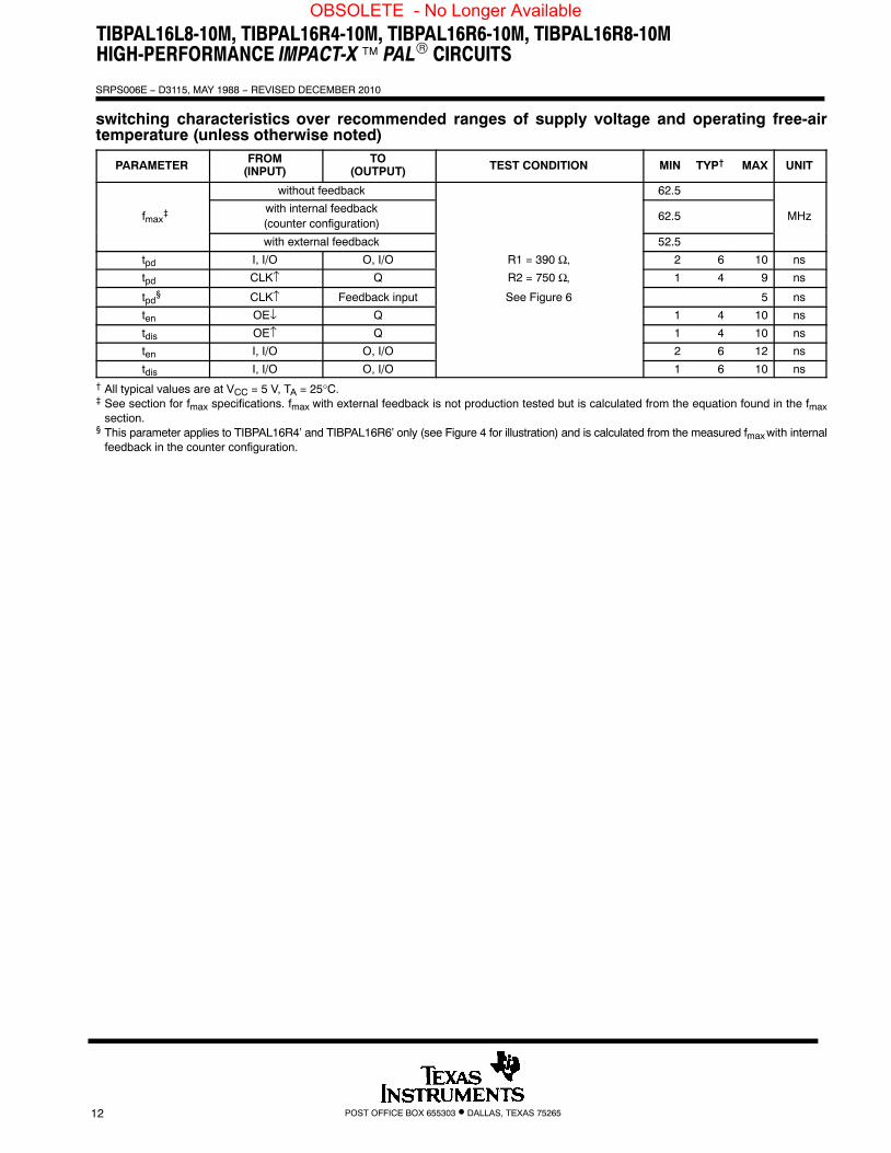
switching characteristics over recommended ranges of supply voltage and operating free-airtemperature (unless otherwise noted)
PARAMETERFROM
(INPUT)TO
(OUTPUT) TEST CONDITION MIN TYP† MAX UNIT
without feedback 62.5
fmax‡ with internal feedback
(counter configuration)62.5 MHz
with external feedback 52.5
tpd I, I/O O, I/O R1 = 390 Ω, 2 6 10 ns
tpd CLK↑ Q R2 = 750 Ω, 1 4 9 ns
tpd§ CLK↑ Feedback input See Figure 6 5 ns
ten OE↓ Q 1 4 10 ns
tdis OE↑ Q 1 4 10 ns
ten I, I/O O, I/O 2 6 12 ns
tdis I, I/O O, I/O 1 6 10 ns† All typical values are at VCC = 5 V, TA = 25°C.‡ See section for fmax specifications. fmax with external feedback is not production tested but is calculated from the equation found in the fmax
section.§ This parameter applies to TIBPAL16R4’ and TIBPAL16R6’ only (see Figure 4 for illustration) and is calculated from the measured fmax with internal
feedback in the counter configuration.
OBSOLETE - No Longer Available
TIBPAL16L8-7C, TIBPAL16R4-7C, TIBPAL16R6-7C, TIBPAL16R8-7CTIBPAL16L8-10M, TIBPAL16R4-10M, TIBPAL16R6-10M, TIBPAL16R8-10M
HIGH-PERFORMANCE IMPACT-X�™ PAL® CIRCUITSSRPS006E − D3115, MAY 1988 − REVISED DECEMBER 2010
POST OFFICE BOX 655303 • DALLAS, TEXAS 75265 13
programming information
Texas Instruments programmable logic devices can be programmed using widely available software andinexpensive device programmers.
Complete programming specifications, algorithms, and the latest information on hardware, software, andfirmware are available upon request. Information on programmers capable of programming Texas Instrumentsprogrammable logic is also available, upon request, from the nearest TI field sales office, local authorized TIdistributor, or by calling Texas Instruments at (214) 997-5666.
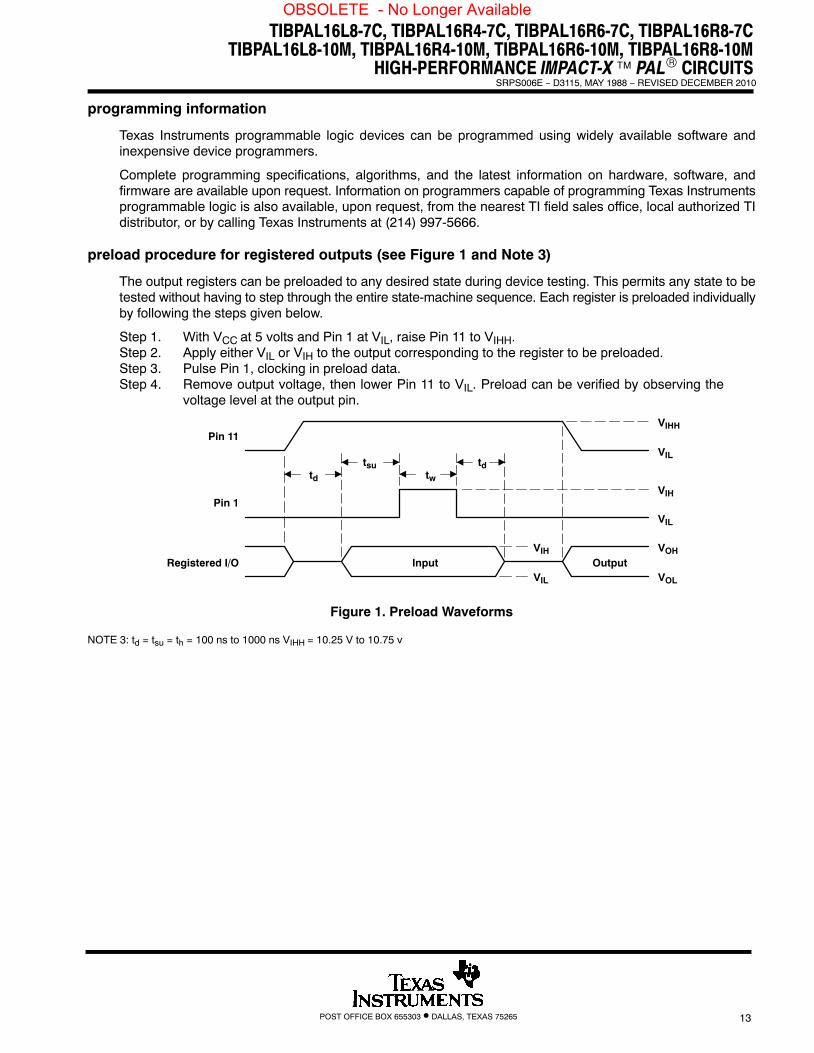
preload procedure for registered outputs (see Figure 1 and Note 3)
The output registers can be preloaded to any desired state during device testing. This permits any state to betested without having to step through the entire state-machine sequence. Each register is preloaded individuallyby following the steps given below.
Step 1. With VCC at 5 volts and Pin 1 at VIL, raise Pin 11 to VIHH.Step 2. Apply either VIL or VIH to the output corresponding to the register to be preloaded.Step 3. Pulse Pin 1, clocking in preload data.Step 4. Remove output voltage, then lower Pin 11 to VIL. Preload can be verified by observing the
voltage level at the output pin.
tdtsu
twtd
VIHH
VIL
VIL
VOL
VOH
VIH
Pin 11
Pin 1
Registered I/O Input OutputVIH
VIL
Figure 1. Preload Waveforms
NOTE 3: td = tsu = th = 100 ns to 1000 ns VIHH = 10.25 V to 10.75 v
OBSOLETE - No Longer Available
TIBPAL16L8-7C, TIBPAL16R4-7C, TIBPAL16R6-7C, TIBPAL16R8-7CTIBPAL16L8-10M, TIBPAL16R4-10M, TIBPAL16R6-10M, TIBPAL16R8-10MHIGH-PERFORMANCE IMPACT-X�™ PAL® CIRCUITSSRPS006E − D3115, MAY 1988 − REVISED DECEMBER 2010
POST OFFICE BOX 655303 • DALLAS, TEXAS 7526514
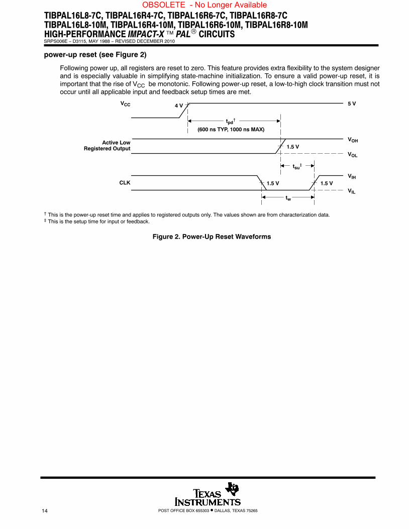
power-up reset (see Figure 2)
Following power up, all registers are reset to zero. This feature provides extra flexibility to the system designerand is especially valuable in simplifying state-machine initialization. To ensure a valid power-up reset, it isimportant that the rise of VCC be monotonic. Following power-up reset, a low-to-high clock transition must notoccur until all applicable input and feedback setup times are met.
1.5 V
tsu‡
tpd†
tw
VIL
VIH
5 VVCC
Active LowRegistered Output
CLK
4 V
VOH
VOL
1.5 V
(600 ns TYP, 1000 ns MAX)
1.5 V
† This is the power-up reset time and applies to registered outputs only. The values shown are from characterization data.‡ This is the setup time for input or feedback.
Figure 2. Power-Up Reset Waveforms
OBSOLETE - No Longer Available
TIBPAL16L8-7C, TIBPAL16R4-7C, TIBPAL16R6-7C, TIBPAL16R8-7CTIBPAL16L8-10M, TIBPAL16R4-10M, TIBPAL16R6-10M, TIBPAL16R8-10M
HIGH-PERFORMANCE IMPACT-X�™ PAL® CIRCUITSSRPS006E − D3115, MAY 1988 − REVISED DECEMBER 2010
POST OFFICE BOX 655303 • DALLAS, TEXAS 75265 15
fmax SPECIFICATIONS
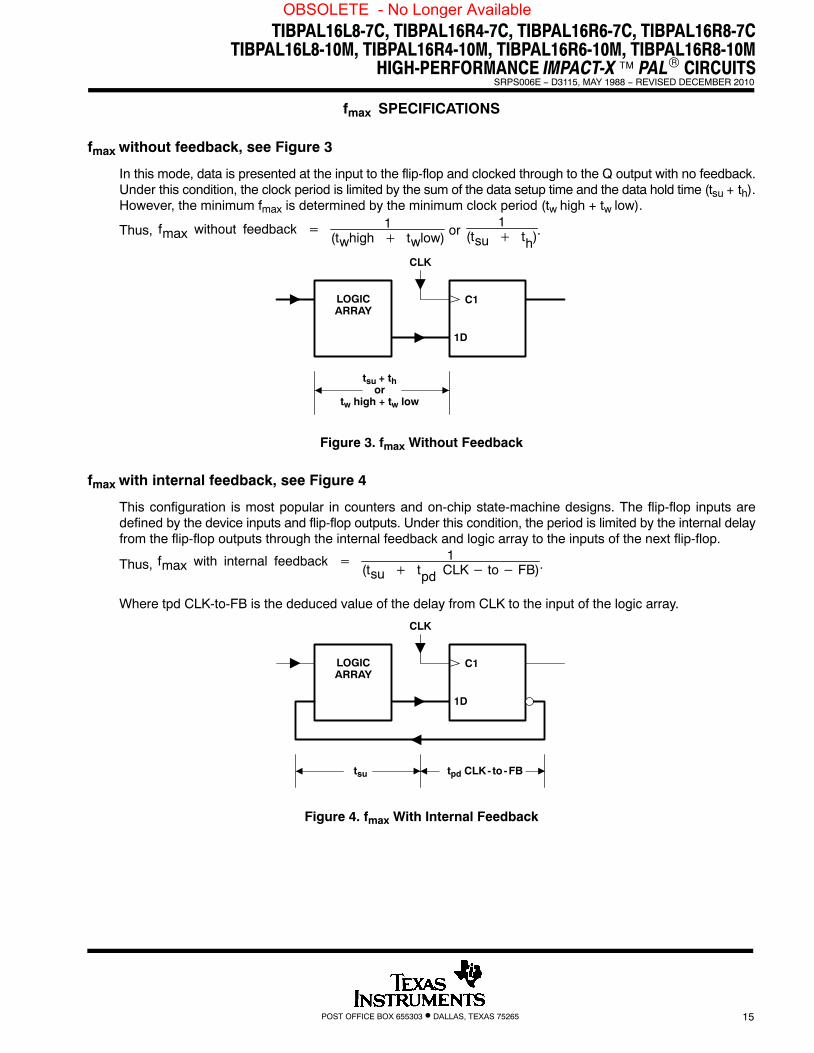
fmax without feedback, see Figure 3
In this mode, data is presented at the input to the flip-flop and clocked through to the Q output with no feedback.Under this condition, the clock period is limited by the sum of the data setup time and the data hold time (tsu + th).However, the minimum fmax is determined by the minimum clock period (tw high + tw low).
Thus, fmax without feedback �1
(twhigh � twlow) or
1(tsu � th).
CLK
LOGICARRAY
tsu + thor
tw high + tw low
C1
1D
Figure 3. fmax Without Feedback
fmax with internal feedback, see Figure 4
This configuration is most popular in counters and on-chip state-machine designs. The flip-flop inputs aredefined by the device inputs and flip-flop outputs. Under this condition, the period is limited by the internal delayfrom the flip-flop outputs through the internal feedback and logic array to the inputs of the next flip-flop.
Thus, fmax with internal feedback �1
(tsu � tpd CLK � to � FB).
Where tpd CLK-to-FB is the deduced value of the delay from CLK to the input of the logic array.
CLK
LOGICARRAY
tsu tpd CLK- to-FB
C1
1D
Figure 4. fmax With Internal Feedback
OBSOLETE - No Longer Available
TIBPAL16L8-7C, TIBPAL16R4-7C, TIBPAL16R6-7C, TIBPAL16R8-7CTIBPAL16L8-10M, TIBPAL16R4-10M, TIBPAL16R6-10M, TIBPAL16R8-10MHIGH-PERFORMANCE IMPACT-X�™ PAL® CIRCUITSSRPS006E − D3115, MAY 1988 − REVISED DECEMBER 2010
POST OFFICE BOX 655303 • DALLAS, TEXAS 7526516
fmax SPECIFICATIONS
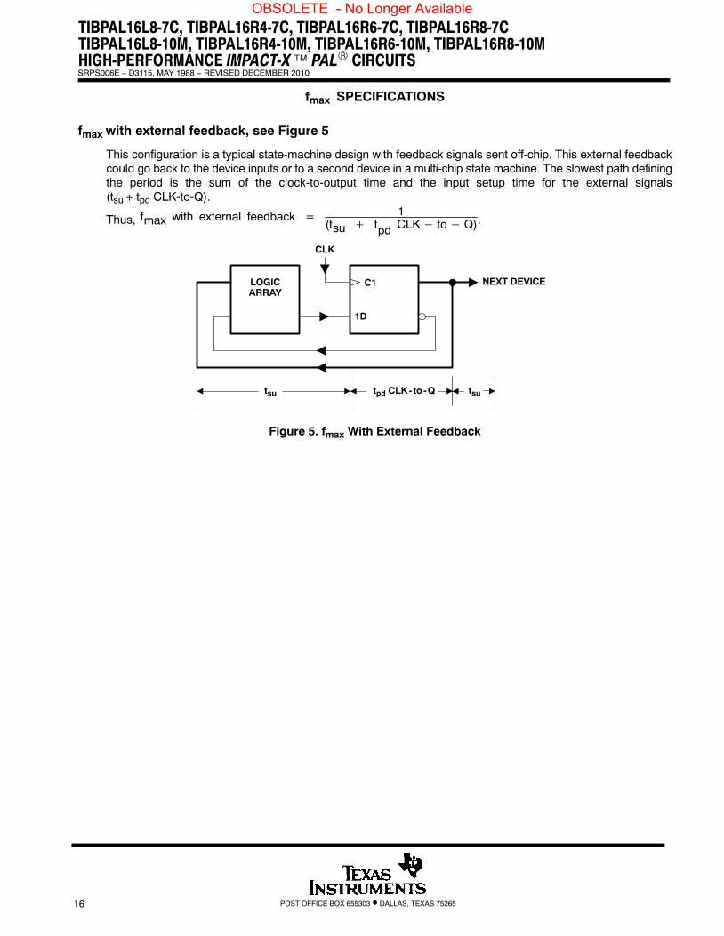
fmax with external feedback, see Figure 5
This configuration is a typical state-machine design with feedback signals sent off-chip. This external feedbackcould go back to the device inputs or to a second device in a multi-chip state machine. The slowest path definingthe period is the sum of the clock-to-output time and the input setup time for the external signals(tsu + tpd CLK-to-Q).
Thus, fmax with external feedback �1
(tsu � tpd CLK � to � Q).
tpd CLK- to -Q tsu
CLK
LOGICARRAY
NEXT DEVICE
tsu
C1
1D
Figure 5. fmax With External Feedback
OBSOLETE - No Longer Available
TIBPAL16L8-7C, TIBPAL16R4-7C, TIBPAL16R6-7C, TIBPAL16R8-7CTIBPAL16L8-10M, TIBPAL16R4-10M, TIBPAL16R6-10M, TIBPAL16R8-10M
HIGH-PERFORMANCE IMPACT-X�™ PAL® CIRCUITSSRPS006E − D3115, MAY 1988 − REVISED DECEMBER 2010
POST OFFICE BOX 655303 • DALLAS, TEXAS 75265 17
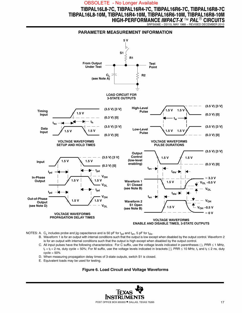
PARAMETER MEASUREMENT INFORMATION
tsu
S1
R2CL(see Note A)
LOAD CIRCUIT FOR3-STATE OUTPUTS
(3.5 V) [3 V]
(0.3 V) [0]
1.5 V
1.5 V
th
1.5 V
tpd
tpd
tpd
tpd
VOLTAGE WAVEFORMSSETUP AND HOLD TIMES
VOLTAGE WAVEFORMSPROPAGATION DELAY TIMES
VOH
VOH
VOL
VOL
1.5 V 1.5 V
1.5 V 1.5 V
tw
1.5 V 1.5 V
≈ 3.3 V
VOL
VOH
VOH −0.5 V
≈ 0 V
ten
ten
tdis
tdis
VOLTAGE WAVEFORMSENABLE AND DISABLE TIMES, 3-STATE OUTPUTS
VOLTAGE WAVEFORMSPULSE DURATIONS
1.5 V 1.5 V
1.5 V
1.5 V 1.5 V
1.5 V 1.5 V
1.5 V
R1
VOL +0.5 V
5 V
(3.5 V) [3 V]
(0.3 V) [0]
(3.5 V) [3 V]
(0.3 V) [0]
(3.5 V) [3 V]
(0.3 V) [0]
(3.5 V) [3 V]
(0.3 V) [0]
(3.5 V) [3 V]
(0.3 V) [0]
From Output Under Test
TestPoint
Input
Out-of-PhaseOutput
(see Note D)
TimingInput
DataInput
In-PhaseOutput
High-LevelPulse
Low-LevelPulse
OutputControl
(low-levelenabling)
Waveform 1S1 Closed
(see Note B)
Waveform 2S1 Open
(see Note B)
NOTES: A. CL includes probe and jig capacitance and is 50 pF for tpd and ten, 5 pF for tdis.B. Waveform 1 is for an output with internal conditions such that the output is low except when disabled by the output control. Waveform 2
is for an output with internal conditions such that the output is high except when disabled by the output control.C. All input pulses have the following characteristics: For C suffix, use the voltage levels indicated in parentheses ( ), PRR ≤ 1 MHz,
tr = tf = 2 ns, duty cycle = 50%; For M suffix, use the voltage levels indicated in brackets [ ], PRR ≤ 10 MHz, tr and tf ≤ 2 ns, dutycycle = 50%
D. When measuring propagation delay times of 3-state outputs, switch S1 is closed.E. Equivalent loads may be used for testing.
Figure 6. Load Circuit and Voltage Waveforms
OBSOLETE - No Longer Available
TIBPAL16L8-7C, TIBPAL16R4-7C, TIBPAL16R6-7C, TIBPAL16R8-7CTIBPAL16L8-10M, TIBPAL16R4-10M, TIBPAL16R6-10M, TIBPAL16R8-10MHIGH-PERFORMANCE IMPACT-X�™ PAL® CIRCUITSSRPS006E − D3115, MAY 1988 − REVISED DECEMBER 2010
POST OFFICE BOX 655303 • DALLAS, TEXAS 7526518
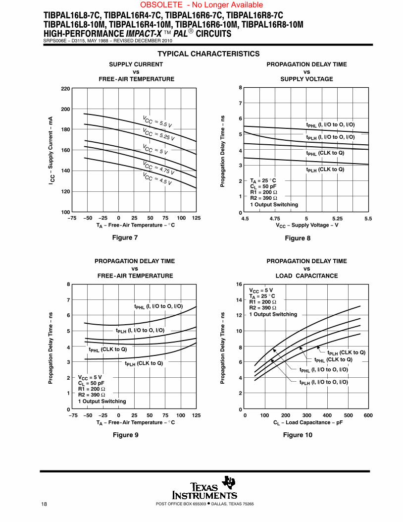
TYPICAL CHARACTERISTICS
160
140
120
100−75 −50 −25 0 25 50
Figure 7
180
200
SUPPLY CURRENTvs
FREE-AIR TEMPERATURE
220
75 100 125TA − Free-Air Temperature − °C
I CC
− S
up
ply
Cu
rren
t −
mA
4
2
1
04.5 4.75 5
Figure 8
Pro
pag
atio
n D
elay
Tim
e −
ns 6
7
PROPAGATION DELAY TIMEvs
SUPPLY VOLTAGE8
5.25 5.5
5
3
VCC − Supply Voltage − V
TA = 25 °CCL = 50 pFR1 = 200 ΩR2 = 390 Ω
tPHL (I, I/O to O, I/O)
tPLH (I, I/O to O, I/O)
tPHL (CLK to Q)
tPLH (CLK to Q)
1 Output Switching
CL − Load Capacitance − pF
4
2
1
0−75 −50 −25 0 25 50
Figure 9
Pro
pag
atio
n D
elay
Tim
e −
ns 6
7
8
75 100 125
5
3
PROPAGATION DELAY TIMEvs
FREE-AIR TEMPERATURE
VCC = 5 VCL = 50 pFR1 = 200 ΩR2 = 390 Ω1 Output Switching
tPHL (I, I/O to O, I/O)
tPLH (I, I/O to O, I/O)
tPHL (CLK to Q)
tPLH (CLK to Q)
TA − Free-Air Temperature − °C
8
4
2
0100 200 300 400
Figure 10
Pro
pag
atio
n D
elay
Tim
e −
ns 12
14
16
500
10
6
PROPAGATION DELAY TIMEvs
LOAD CAPACITANCE
tPHL (I, I/O to O, I/O)
tPLH (I, I/O to O, I/O)
tPHL (CLK to Q)tPLH (CLK to Q)
VCC = 5 VTA = 25 °CR1 = 200 ΩR2 = 390 Ω1 Output Switching
0 600
OBSOLETE - No Longer Available
TIBPAL16L8-7C, TIBPAL16R4-7C, TIBPAL16R6-7C, TIBPAL16R8-7CTIBPAL16L8-10M, TIBPAL16R4-10M, TIBPAL16R6-10M, TIBPAL16R8-10M
HIGH-PERFORMANCE IMPACT-X�™ PAL® CIRCUITSSRPS006E − D3115, MAY 1988 − REVISED DECEMBER 2010
POST OFFICE BOX 655303 • DALLAS, TEXAS 75265 19
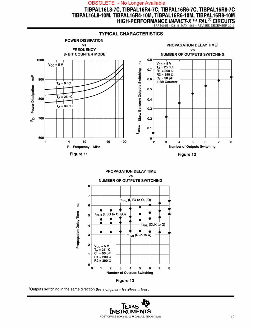
TYPICAL CHARACTERISTICS
Number of Outputs Switching
0.4
0.2
0.1
02 3 4 5 6
Figure 12
0.6
0.7
0.8
7 8
0.5
0.3
PROPAGATION DELAY TIME†
vsNUMBER OF OUTPUTS SWITCHING
VCC = 5 VTA = 25 °CR1 = 200 ΩR2 = 390 ΩCL = 50 pF8-Bit Counter
4
2
1
00 1 2 3 4 5
Figure 13
Pro
pag
atio
n D
elay
Tim
e −
ns 6
7
8
6 7 8
5
3
PROPAGATION DELAY TIMEvs
NUMBER OF OUTPUTS SWITCHING
t skew
− S
kew
Bet
wee
n O
utp
uts
Sw
itch
ing
− n
s
VCC = 5 VTA = 25 °CCL = 50 pFR1 = 200 ΩR2 = 390 Ω
Number of Outputs Switching
tPHL (I, I/O to O, I/O)
tPLH (I, I/O to O, I/O)
tPHL (CLK to Q)
tPLH (CLK to Q)
1 4 10 40 100
Figure 11
F − Frequency − MHz
POWER DISSIPATIONvs
FREQUENCY8-BIT COUNTER MODE
800
600
1000
700
900
VCC = 5 V
P D −
Po
wer
Dis
sip
atio
n −
mW
TA = 0 °C
TA = 25 °C
TA = 80 °C
†Outputs switching in the same direction (tPLH compared to tPLH/tPHL to tPHL)
OBSOLETE - No Longer Available
D0892
North AmericanTI Authorized
Distributors
CustomerResponse CenterTOLL FREE: (800) 336-5236OUTSIDE USA: (214) 995-6611
(8:00 a.m. − 5:00 p.m. CST)
TI Die ProcessorsChip Supply (407) 298-7100Elmo Semiconductor (818) 768-7400Minco Technology Labs (512) 834-2022
©1992 Texas Instruments Incorporated
Printed in U.S.A. SRPS006D
TI NorthAmerican SalesOfficesALABAMA: Huntsville: (205) 837-7530ARIZONA: Phoenix: (602) 995-1007CALIFORNIA: Irvine: (714) 660-1200San Diego: (619) 278-9600Santa Clara: (408) 980-9000Woodland Hills: (818) 704-8100COLORADO: Aurora: (303) 368-8000CONNECTICUT: Wallingford: (203) 269-0074FLORIDA: Altamonte Springs: (407) 260-2116Fort Lauderdale: (305) 973-8502Tampa: (813) 885-7588GEORGIA: Norcross: (404) 662-7967ILLINOIS: Arlington Heights: (708) 640-3000INDIANA: Carmel: (317) 573-6400Fort Wayne: (219) 489-4697KANSAS: Overland Park: (913) 451-4511MARYLAND: Columbia: (410) 964-2003MASSACHUSETTS: Waltham: (617) 895-9100MICHIGAN: Farmington Hills: (313) 553-1581MINNESOTA: Eden Prairie: (612) 828-9300MISSOURI: St. Louis: (314) 821-8400NEW JERSEY: Iselin: (908) 750-1050NEW MEXICO: Albuquerque: (505) 345-2555NEW YORK: East Syracuse: (315) 463-9291Fishkill: (914) 897-2900Melville: (516) 454-6600Pittsford: (716) 385-6770NORTH CAROLINA: Charlotte: (704) 527-0930Raleigh: (919) 876-2725OHIO: Beachwood: (216) 765-7258Beavercreek: (513) 427-6200OREGON: Beaverton: (503) 643-6758PENNSYLVANIA: Blue Bell: (215) 825-9500PUERTO RICO: Hato Rey: (809) 753-8700TEXAS: Austin: (512) 250-6769Dallas: (214) 917-1264Houston: (713) 778-6592Midland: (915) 561-7137UTAH: Salt Lake CIty: (801) 466-8972WISCONSIN: Waukesha: (414) 798-1001CANADA: Nepean: (613) 726-1970Richmond Hill: (416) 884-9181St. Laurent: (514) 335-8392
TI RegionalTechnologyCentersCALIFORNIA: Irvine: (714) 660-8140 Santa Clara: (408) 748-2222GEORGIA: Norcross: (404) 662-7945ILLINOIS: Arlington Heights: (708) 640-2909INDIANA: Indianapolis: (317) 573-6400MASSACHUSETTS: Waltham: (617) 895-9196MEXICO: Mexico City: 491-70834MINNESOTA: Minneapolis: (612) 828-9300TEXAS: Dallas: (214) 917-3881CANADA: Nepean: (613) 726-1970
Alliance Electronics, Inc. (military product only)Almac/ArrowAnthem Electronics Arrow/SchweberFuture Electronics (Canada) GRS Electronics Co., Inc. Hall-Mark Electronics Marshall Industries Newark Electronics Rochester Electronics, Inc. (obsolete product only (508) 462-9332) Wyle Laboratories Zeus Components
TI DistributorsALABAMA: Arrow/Schweber (205) 837-6955; Hall-Mark(205) 837-8700; Marshall (205) 881-9235.ARIZONA: Anthem (602) 966-6600; Arrow/Schweber (602)437-0750; Hall-Mark (602) 431-0030; Marshall (602)496-0290; Wyle (602) 437-2088.CALIFORNIA: Los Angeles/Orange County: Anthem(818) 775-1333, (714) 768-4444; Arrow/Schweber (818)380-9686, (714) 838-5422; Hall-Mark (818) 773-4500, (714)727-6000; Marshall (818) 878-7000, (714) 458-5301; Wyle(818) 880-9000, (714) 863-9953; Zeus (714) 921-9000,(818) 889-3838;Sacramento: Anthem (916) 624-9744; Hall-Mark (916)624-9781; Marshall (916) 635-9700; Wyle (916) 638-5282;San Diego: Anthem (619) 453-9005; Arrow/Schweber(619) 565-4800; Hall-Mark (619) 268-1201; Marshall (619)578-9600; Wyle (619) 565-9171; Zeus (619) 277-9681.San Francisco Bay Area: Anthem (408) 453-1200;Arrow/Schweber (408) 441-9700, (510) 490-9477;Hall-Mark (408) 432-4000; Marshall (408) 942-4600;Wyle (408) 727-2500; Zeus (408) 629-4789.COLORADO: Anthem (303) 790-4500; Arrow/Schweber(303) 799-0258; Hall-Mark (303) 790-1662; Marshall (303)451-8383; Wyle (303) 457-9953.CONNECTICUT: Anthem (203) 575-1575; Arrow/Schweber(203) 265-7741; Hall-Mark (203) 271-2844; Marshall (203)265-3822.FLORIDA: Fort Lauderdale: Arrow/Schweber (305)429-8200; Halll-Mark (305) 971-9280; Marshall (305)977-4880.Orlando: Arrow/Schweber (407) 333-9300; Hall-Mark (407)830-5855; Marshall (407) 767-8585; Zeus (407) 788-9100.Tampa: Hall-Mark (813) 541-7440; Marshall (813)573-1399.GEORGIA: Arrow/Schweber (404) 497-1300; Hall-Mark(404) 623-4400; Marshall (404) 923-5750.ILLINOIS: Anthem (708) 884-0200; Arrow/Schweber (708)250-0500; Hall-Mark (312) 860-3800; Marshall (708)490-0155; Newark (312)784-5100.INDIANA: Arrow/Schweber (317) 299-2071; Hall-Mark(317) 872-8875; Marshall (317) 297-0483.IOWA: Arrow/Schweber (319) 395-7230.KANSAS: Arrow/Schweber (913) 541-9542; Hall-Mark(913) 888-4747; Marshall (913) 492-3121.MARYLAND: Anthem (301) 995-6640; Arrow/Schweber(301) 596-7800; Hall-Mark (301) 988-9800; Marshall (301)622-1118; Zeus (301) 997-1118.MASSACHUSETTS: Anthem (508) 657-5170;Arrow/Schweber (508) 658-0900; Hall-Mark (508)667-0902; Marshall (508) 658-0810; Wyle (617) 272-7300;Zeus (617) 246-8200.
MICHIGAN: Detroit: Arrow/Schweber (313) 462-2290;Hall-Mark (313) 416-5800; Marshall (313) 525-5850;Newark (313) 967-0600.MINNESOTA: Anthem (612) 944-5454; Arrow/Schweber(612) 941-5280; Hall-Mark (612) 881-2600; Marshall (612)559-2211.MISSOURI: Arrow/Schweber (314) 567-6888; Hall-Mark(314) 291-5350; Marshall (314) 291-4650.NEW JERSEY: Anthem (201) 227-7960; Arrow/Schweber(201) 227-7880, (609) 596-8000; Hall-Mark (201) 515-3000,(609) 235-1900; Marshall (201) 882-0320, (609) 234-9100.NEW MEXICO: Alliance (505) 292-3360.NEW YORK: Long Island: Anthem (516) 864-6600;Arrow/Schweber (516) 231-1000; Hall-Mark (516)737-0600; Marshall (516) 273-2424; Zeus (914) 937-7400.Rochester: Arrow/Schweber (716) 427-0300; Hall-Mark(716) 425-3300; Marshall (716) 235-7620.Syracuse: Marshall (607) 785-2345.NORTH CAROLINA: Arrow/Schweber (919) 876-3132;Hall-Mark (919) 872-0712; Marshall (919) 878-9882.OHIO: Cleveland: Arrow/Schweber (216) 248-3990;Hall-Mark (216) 349-4632; Marshall (216) 248-1788.Columbus: Hall-Mark (614) 888-3313.Dayton: Arrow/Schweber (513) 435-5563; Marshall (513)898-4480; Zeus (513) 293-6162.OKLAHOMA: Arrow/Schweber (918) 252-7537; Hall-Mark(918) 254-6110.OREGON: Almac/Arrow (503) 629-8090; Anthem (503)643-1114; Marshall (503) 644-5050; Wyle (503) 643-7900.PENNSYLVANIA: Anthem (215) 443-5150;Arrow/Schweber (215) 928-1800; GRS (215) 922-7037;(609) 964-8560; Marshall (412) 788-0441.TEXAS: Austin: Arrow/Schweber (512) 835-4180;Hall-Mark (512) 258-8848; Marshall (512) 837-1991; Wyle(512) 345-8853;Dallas: Anthem (214) 238-7100; Arrow/Schweber (214)380-6464; Hall-Mark (214) 553-4300; Marshall (214)233-5200; Wyle (214) 235-9953; Zeus (214) 783-7010;Houston: Arrow/Schweber (713) 530-4700; Hall-Mark (713) 781-6100; Marshall (713) 467-1666; Wyle (713)879-9953.UTAH: Anthem (801) 973-8555; Arrow/Schweber (801)973-6913; Marshall (801) 973-2288; Wyle (801) 974-9953.WASHINGTON: Almac/Arrow (206) 643-9992, Anthem(206) 483-1700; Marshall (206) 486-5747; Wyle (206)881-1150.WISCONSIN: Arrow/Schweber (414) 792-0150; Hall-Mark(414) 797-7844; Marshall (414) 797-8400.CANADA: Calgary: Future (403) 235-5325;Edmonton: Future (403) 438-2858;Montreal: Arrow/Schweber (514) 421-7411; Future (514)694-7710; Marshall (514) 694-8142Ottawa: Arrow/Schweber (613) 226-6903; Future (613)820-8313.Quebec: Future (418) 897-6666.Toronto: Arrow/Schweber (416) 670-7769; Future (416) 612-9200; Marshall (416) 458-8046.Vancouver: Arrow/Schweber (604) 421-2333; Future (604) 294-1166.
OBSOLETE - No Longer Available
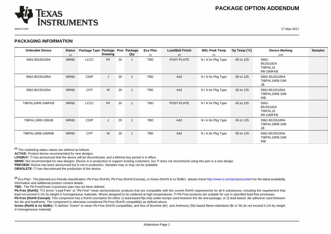
PACKAGE OPTION ADDENDUM
www.ti.com 17-Mar-2017
Addendum-Page 1
PACKAGING INFORMATION
Orderable Device Status(1)
Package Type PackageDrawing
Pins PackageQty
Eco Plan(2)
Lead/Ball Finish(6)
MSL Peak Temp(3)
Op Temp (°C) Device Marking(4/5)
Samples
5962-85155182A NRND LCCC FK 20 1 TBD POST-PLATE N / A for Pkg Type -55 to 125 5962-85155182ATIBPAL16R8-10MFKB
5962-8515518RA NRND CDIP J 20 1 TBD A42 N / A for Pkg Type -55 to 125 5962-8515518RATIBPAL16R8-10MJB
5962-8515518SA NRND CFP W 20 1 TBD A42 N / A for Pkg Type -55 to 125 5962-8515518SATIBPAL16R8-10MWB
TIBPAL16R8-10MFKB NRND LCCC FK 20 1 TBD POST-PLATE N / A for Pkg Type -55 to 125 5962-85155182ATIBPAL16R8-10MFKB
TIBPAL16R8-10MJB NRND CDIP J 20 1 TBD A42 N / A for Pkg Type -55 to 125 5962-8515518RATIBPAL16R8-10MJB
TIBPAL16R8-10MWB NRND CFP W 20 1 TBD A42 N / A for Pkg Type -55 to 125 5962-8515518SATIBPAL16R8-10MWB
(1) The marketing status values are defined as follows:ACTIVE: Product device recommended for new designs.LIFEBUY: TI has announced that the device will be discontinued, and a lifetime-buy period is in effect.NRND: Not recommended for new designs. Device is in production to support existing customers, but TI does not recommend using this part in a new design.PREVIEW: Device has been announced but is not in production. Samples may or may not be available.OBSOLETE: TI has discontinued the production of the device.
(2) Eco Plan - The planned eco-friendly classification: Pb-Free (RoHS), Pb-Free (RoHS Exempt), or Green (RoHS & no Sb/Br) - please check http://www.ti.com/productcontent for the latest availabilityinformation and additional product content details.TBD: The Pb-Free/Green conversion plan has not been defined.Pb-Free (RoHS): TI's terms "Lead-Free" or "Pb-Free" mean semiconductor products that are compatible with the current RoHS requirements for all 6 substances, including the requirement thatlead not exceed 0.1% by weight in homogeneous materials. Where designed to be soldered at high temperatures, TI Pb-Free products are suitable for use in specified lead-free processes.Pb-Free (RoHS Exempt): This component has a RoHS exemption for either 1) lead-based flip-chip solder bumps used between the die and package, or 2) lead-based die adhesive used betweenthe die and leadframe. The component is otherwise considered Pb-Free (RoHS compatible) as defined above.Green (RoHS & no Sb/Br): TI defines "Green" to mean Pb-Free (RoHS compatible), and free of Bromine (Br) and Antimony (Sb) based flame retardants (Br or Sb do not exceed 0.1% by weightin homogeneous material)
PACKAGE OPTION ADDENDUM
www.ti.com 17-Mar-2017
Addendum-Page 2
(3) MSL, Peak Temp. - The Moisture Sensitivity Level rating according to the JEDEC industry standard classifications, and peak solder temperature.
(4) There may be additional marking, which relates to the logo, the lot trace code information, or the environmental category on the device.
(5) Multiple Device Markings will be inside parentheses. Only one Device Marking contained in parentheses and separated by a "~" will appear on a device. If a line is indented then it is a continuationof the previous line and the two combined represent the entire Device Marking for that device.
(6) Lead/Ball Finish - Orderable Devices may have multiple material finish options. Finish options are separated by a vertical ruled line. Lead/Ball Finish values may wrap to two lines if the finishvalue exceeds the maximum column width.
Important Information and Disclaimer:The information provided on this page represents TI's knowledge and belief as of the date that it is provided. TI bases its knowledge and belief on informationprovided by third parties, and makes no representation or warranty as to the accuracy of such information. Efforts are underway to better integrate information from third parties. TI has taken andcontinues to take reasonable steps to provide representative and accurate information but may not have conducted destructive testing or chemical analysis on incoming materials and chemicals.TI and TI suppliers consider certain information to be proprietary, and thus CAS numbers and other limited information may not be available for release.
In no event shall TI's liability arising out of such information exceed the total purchase price of the TI part(s) at issue in this document sold by TI to Customer on an annual basis.
IMPORTANT NOTICE
Texas Instruments Incorporated (TI) reserves the right to make corrections, enhancements, improvements and other changes to itssemiconductor products and services per JESD46, latest issue, and to discontinue any product or service per JESD48, latest issue. Buyersshould obtain the latest relevant information before placing orders and should verify that such information is current and complete.TI’s published terms of sale for semiconductor products (http://www.ti.com/sc/docs/stdterms.htm) apply to the sale of packaged integratedcircuit products that TI has qualified and released to market. Additional terms may apply to the use or sale of other types of TI products andservices.Reproduction of significant portions of TI information in TI data sheets is permissible only if reproduction is without alteration and isaccompanied by all associated warranties, conditions, limitations, and notices. TI is not responsible or liable for such reproduceddocumentation. Information of third parties may be subject to additional restrictions. Resale of TI products or services with statementsdifferent from or beyond the parameters stated by TI for that product or service voids all express and any implied warranties for theassociated TI product or service and is an unfair and deceptive business practice. TI is not responsible or liable for any such statements.Buyers and others who are developing systems that incorporate TI products (collectively, “Designers”) understand and agree that Designersremain responsible for using their independent analysis, evaluation and judgment in designing their applications and that Designers havefull and exclusive responsibility to assure the safety of Designers' applications and compliance of their applications (and of all TI productsused in or for Designers’ applications) with all applicable regulations, laws and other applicable requirements. Designer represents that, withrespect to their applications, Designer has all the necessary expertise to create and implement safeguards that (1) anticipate dangerousconsequences of failures, (2) monitor failures and their consequences, and (3) lessen the likelihood of failures that might cause harm andtake appropriate actions. Designer agrees that prior to using or distributing any applications that include TI products, Designer willthoroughly test such applications and the functionality of such TI products as used in such applications.TI’s provision of technical, application or other design advice, quality characterization, reliability data or other services or information,including, but not limited to, reference designs and materials relating to evaluation modules, (collectively, “TI Resources”) are intended toassist designers who are developing applications that incorporate TI products; by downloading, accessing or using TI Resources in anyway, Designer (individually or, if Designer is acting on behalf of a company, Designer’s company) agrees to use any particular TI Resourcesolely for this purpose and subject to the terms of this Notice.TI’s provision of TI Resources does not expand or otherwise alter TI’s applicable published warranties or warranty disclaimers for TIproducts, and no additional obligations or liabilities arise from TI providing such TI Resources. TI reserves the right to make corrections,enhancements, improvements and other changes to its TI Resources. TI has not conducted any testing other than that specificallydescribed in the published documentation for a particular TI Resource.Designer is authorized to use, copy and modify any individual TI Resource only in connection with the development of applications thatinclude the TI product(s) identified in such TI Resource. NO OTHER LICENSE, EXPRESS OR IMPLIED, BY ESTOPPEL OR OTHERWISETO ANY OTHER TI INTELLECTUAL PROPERTY RIGHT, AND NO LICENSE TO ANY TECHNOLOGY OR INTELLECTUAL PROPERTYRIGHT OF TI OR ANY THIRD PARTY IS GRANTED HEREIN, including but not limited to any patent right, copyright, mask work right, orother intellectual property right relating to any combination, machine, or process in which TI products or services are used. Informationregarding or referencing third-party products or services does not constitute a license to use such products or services, or a warranty orendorsement thereof. Use of TI Resources may require a license from a third party under the patents or other intellectual property of thethird party, or a license from TI under the patents or other intellectual property of TI.TI RESOURCES ARE PROVIDED “AS IS” AND WITH ALL FAULTS. TI DISCLAIMS ALL OTHER WARRANTIES ORREPRESENTATIONS, EXPRESS OR IMPLIED, REGARDING RESOURCES OR USE THEREOF, INCLUDING BUT NOT LIMITED TOACCURACY OR COMPLETENESS, TITLE, ANY EPIDEMIC FAILURE WARRANTY AND ANY IMPLIED WARRANTIES OFMERCHANTABILITY, FITNESS FOR A PARTICULAR PURPOSE, AND NON-INFRINGEMENT OF ANY THIRD PARTY INTELLECTUALPROPERTY RIGHTS. TI SHALL NOT BE LIABLE FOR AND SHALL NOT DEFEND OR INDEMNIFY DESIGNER AGAINST ANY CLAIM,INCLUDING BUT NOT LIMITED TO ANY INFRINGEMENT CLAIM THAT RELATES TO OR IS BASED ON ANY COMBINATION OFPRODUCTS EVEN IF DESCRIBED IN TI RESOURCES OR OTHERWISE. IN NO EVENT SHALL TI BE LIABLE FOR ANY ACTUAL,DIRECT, SPECIAL, COLLATERAL, INDIRECT, PUNITIVE, INCIDENTAL, CONSEQUENTIAL OR EXEMPLARY DAMAGES INCONNECTION WITH OR ARISING OUT OF TI RESOURCES OR USE THEREOF, AND REGARDLESS OF WHETHER TI HAS BEENADVISED OF THE POSSIBILITY OF SUCH DAMAGES.Unless TI has explicitly designated an individual product as meeting the requirements of a particular industry standard (e.g., ISO/TS 16949and ISO 26262), TI is not responsible for any failure to meet such industry standard requirements.Where TI specifically promotes products as facilitating functional safety or as compliant with industry functional safety standards, suchproducts are intended to help enable customers to design and create their own applications that meet applicable functional safety standardsand requirements. Using products in an application does not by itself establish any safety features in the application. Designers mustensure compliance with safety-related requirements and standards applicable to their applications. Designer may not use any TI products inlife-critical medical equipment unless authorized officers of the parties have executed a special contract specifically governing such use.Life-critical medical equipment is medical equipment where failure of such equipment would cause serious bodily injury or death (e.g., lifesupport, pacemakers, defibrillators, heart pumps, neurostimulators, and implantables). Such equipment includes, without limitation, allmedical devices identified by the U.S. Food and Drug Administration as Class III devices and equivalent classifications outside the U.S.TI may expressly designate certain products as completing a particular qualification (e.g., Q100, Military Grade, or Enhanced Product).Designers agree that it has the necessary expertise to select the product with the appropriate qualification designation for their applicationsand that proper product selection is at Designers’ own risk. Designers are solely responsible for compliance with all legal and regulatoryrequirements in connection with such selection.Designer will fully indemnify TI and its representatives against any damages, costs, losses, and/or liabilities arising out of Designer’s non-compliance with the terms and provisions of this Notice.
Mailing Address: Texas Instruments, Post Office Box 655303, Dallas, Texas 75265Copyright © 2017, Texas Instruments Incorporated