Embed Size (px)
Citation preview
Lecture #2 Operational Amplifiers
Instructor: Dr. Ahmad El-Banna
Benha University Faculty of Engineering at Shoubra
Spr
in
g 2
015
ECE-322 Electronic Circuits (B)
© A
hmad
El-B
anna
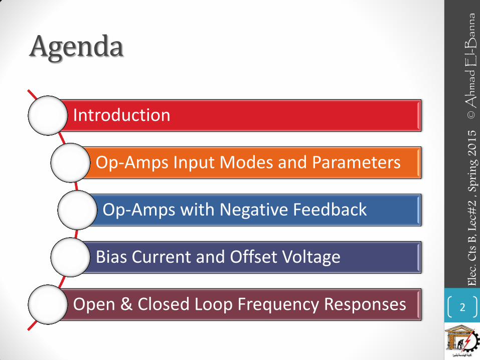
Agenda
Introduction
Op-Amps Input Modes and Parameters
Op-Amps with Negative Feedback
Bias Current and Offset Voltage
Open & Closed Loop Frequency Responses 2
Elec.
Cts B
, Lec
#2 , S
prin
g 201
5 ©
Ahm
ad E
l-Ban
na
INTRODUCTION 3
© A
hmad
El-B
anna
Ele
c. Ct
s B, L
ec#2
, Spr
ing 2
015
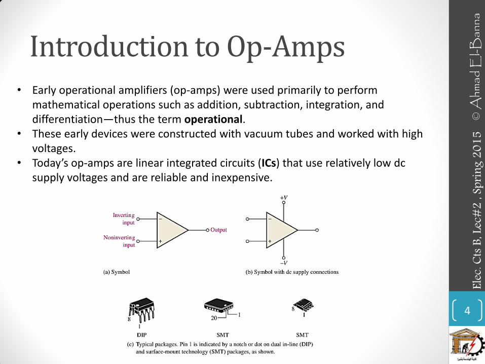
Introduction to Op-Amps
4
© A
hmad
El-B
anna
Ele
c. Ct
s B, L
ec#2
, Spr
ing 2
015
• Early operational amplifiers (op-amps) were used primarily to perform mathematical operations such as addition, subtraction, integration, and differentiation—thus the term operational.
• These early devices were constructed with vacuum tubes and worked with high voltages.
• Today’s op-amps are linear integrated circuits (ICs) that use relatively low dc supply voltages and are reliable and inexpensive.
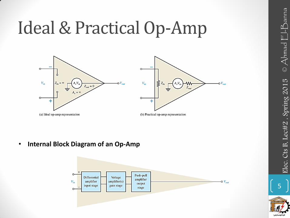
Ideal & Practical Op-Amp
5
© A
hmad
El-B
anna
Ele
c. Ct
s B, L
ec#2
, Spr
ing 2
015
• Internal Block Diagram of an Op-Amp
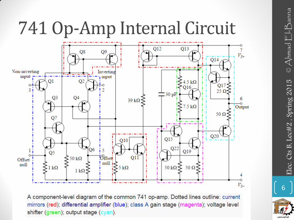
741 Op-Amp Internal Circuit
6
© A
hmad
El-B
anna
Ele
c. Ct
s B, L
ec#2
, Spr
ing 2
015
OP-AMPS INPUT MODES AND PARAMETERS
7
© A
hmad
El-B
anna
Ele
c. Ct
s B, L
ec#2
, Spr
ing 2
015
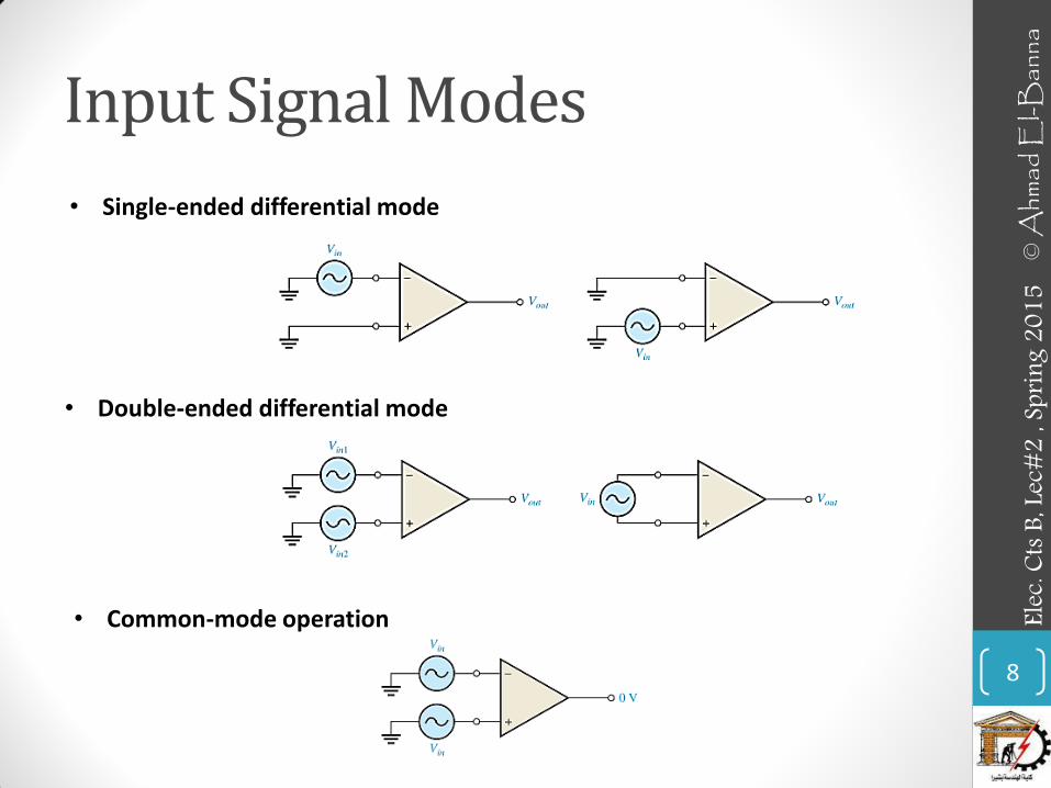
Input Signal Modes
8
© A
hmad
El-B
anna
Ele
c. Ct
s B, L
ec#2
, Spr
ing 2
015
• Common-mode operation
• Double-ended differential mode
• Single-ended differential mode
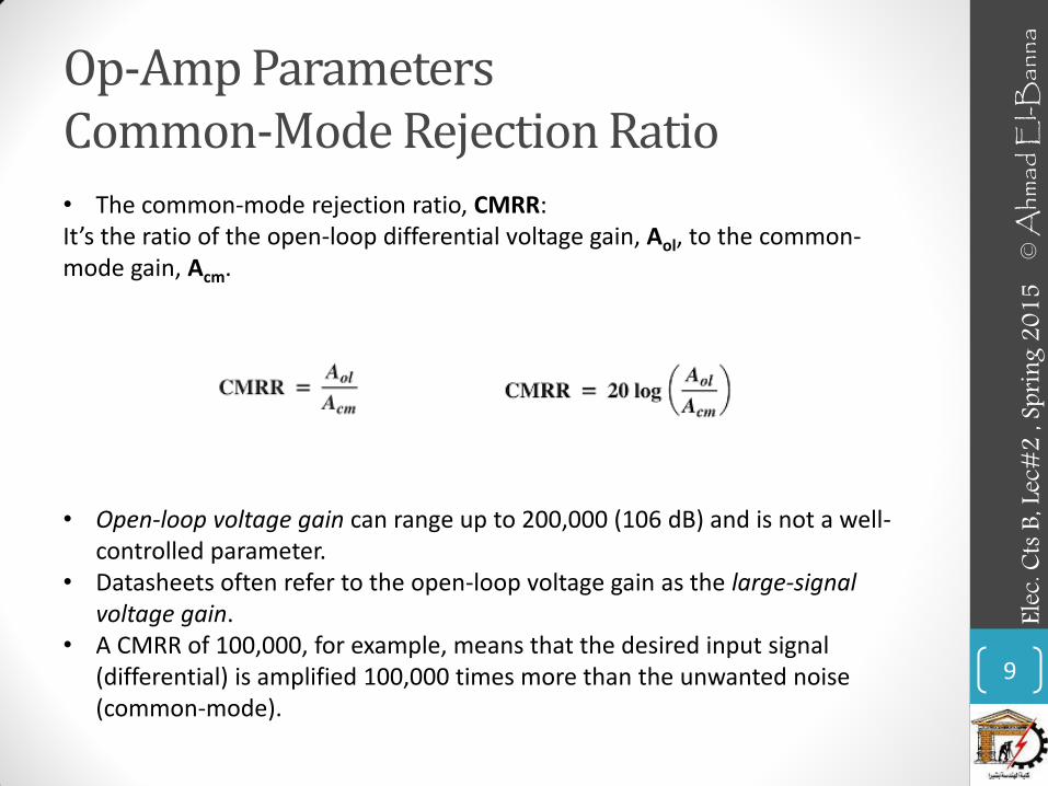
Op-Amp Parameters Common-Mode Rejection Ratio
9
© A
hmad
El-B
anna
Ele
c. Ct
s B, L
ec#2
, Spr
ing 2
015
• The common-mode rejection ratio, CMRR: It’s the ratio of the open-loop differential voltage gain, Aol, to the common-mode gain, Acm.
• Open-loop voltage gain can range up to 200,000 (106 dB) and is not a well-controlled parameter.
• Datasheets often refer to the open-loop voltage gain as the large-signal voltage gain.
• A CMRR of 100,000, for example, means that the desired input signal (differential) is amplified 100,000 times more than the unwanted noise (common-mode).
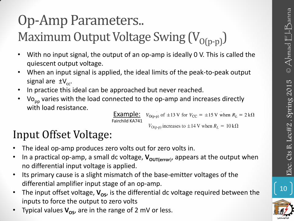
Op-Amp Parameters.. Maximum Output Voltage Swing (VO(p-p))
10
© A
hmad
El-B
anna
Ele
c. Ct
s B, L
ec#2
, Spr
ing 2
015
• With no input signal, the output of an op-amp is ideally 0 V. This is called the quiescent output voltage.
• When an input signal is applied, the ideal limits of the peak-to-peak output signal are ±Vcc.
• In practice this ideal can be approached but never reached. • Vopp varies with the load connected to the op-amp and increases directly
with load resistance.
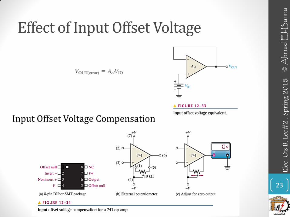
Input Offset Voltage: • The ideal op-amp produces zero volts out for zero volts in. • In a practical op-amp, a small dc voltage, VOUT(error), appears at the output when
no differential input voltage is applied. • Its primary cause is a slight mismatch of the base-emitter voltages of the
differential amplifier input stage of an op-amp. • The input offset voltage, VOS, is the differential dc voltage required between the
inputs to force the output to zero volts • Typical values VOS, are in the range of 2 mV or less.
Example: Fairchild KA741
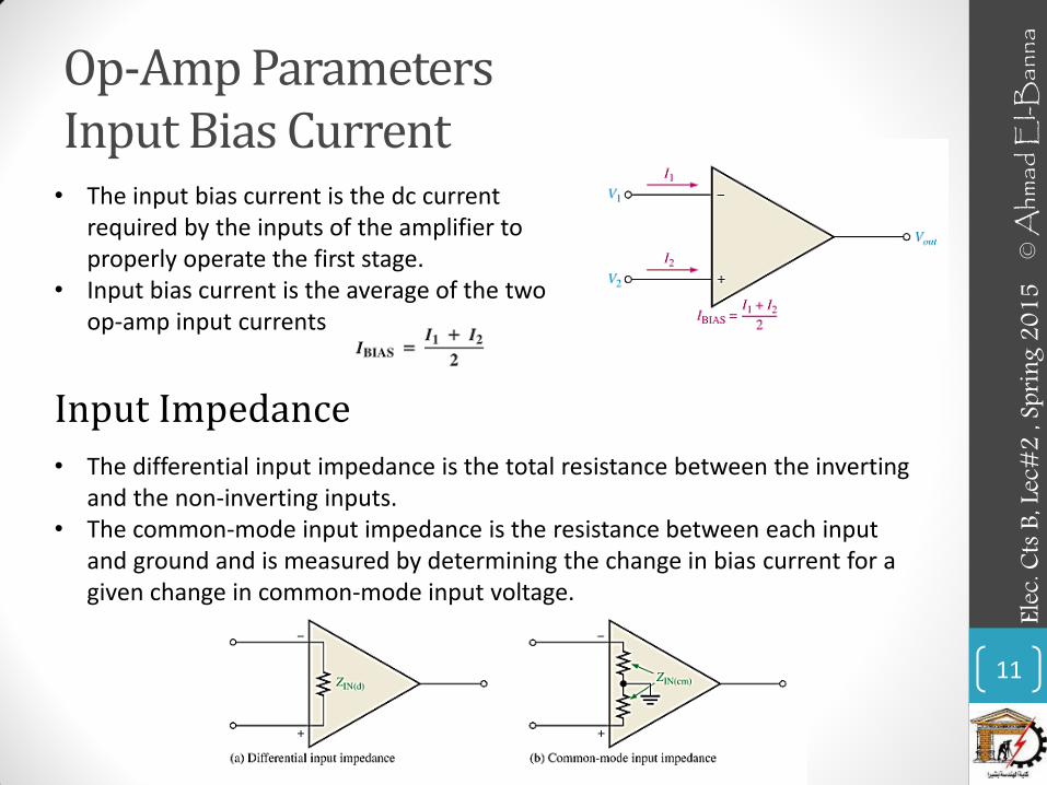
Op-Amp Parameters Input Bias Current
11
© A
hmad
El-B
anna
Ele
c. Ct
s B, L
ec#2
, Spr
ing 2
015
• The input bias current is the dc current required by the inputs of the amplifier to properly operate the first stage.
• Input bias current is the average of the two op-amp input currents
Input Impedance
• The differential input impedance is the total resistance between the inverting and the non-inverting inputs.
• The common-mode input impedance is the resistance between each input and ground and is measured by determining the change in bias current for a given change in common-mode input voltage.
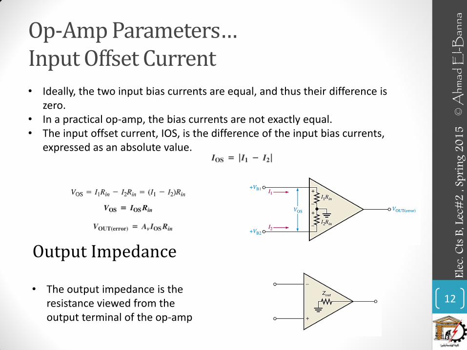
Op-Amp Parameters… Input Offset Current
12
© A
hmad
El-B
anna
Ele
c. Ct
s B, L
ec#2
, Spr
ing 2
015
• Ideally, the two input bias currents are equal, and thus their difference is zero.
• In a practical op-amp, the bias currents are not exactly equal. • The input offset current, IOS, is the difference of the input bias currents,
expressed as an absolute value.
Output Impedance
• The output impedance is the resistance viewed from the output terminal of the op-amp
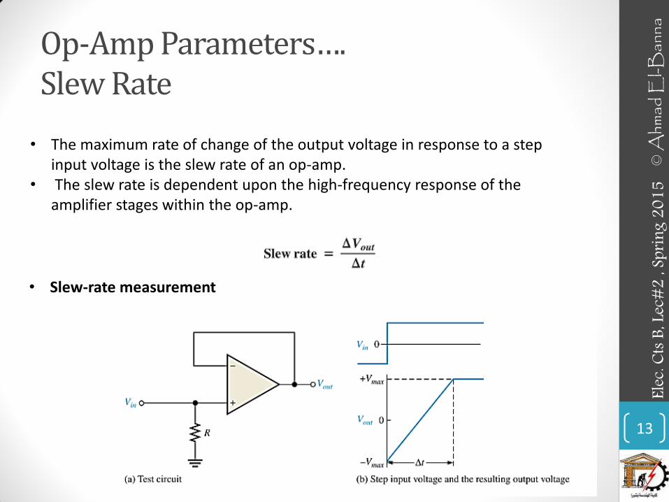
Op-Amp Parameters…. Slew Rate
13
© A
hmad
El-B
anna
Ele
c. Ct
s B, L
ec#2
, Spr
ing 2
015
• Slew-rate measurement
• The maximum rate of change of the output voltage in response to a step input voltage is the slew rate of an op-amp.
• The slew rate is dependent upon the high-frequency response of the amplifier stages within the op-amp.
Op-Amp Parameters….. Frequency Response
14
© A
hmad
El-B
anna
Ele
c. Ct
s B, L
ec#2
, Spr
ing 2
015
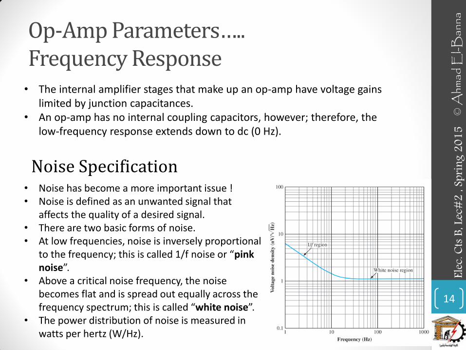
• The internal amplifier stages that make up an op-amp have voltage gains limited by junction capacitances.
• An op-amp has no internal coupling capacitors, however; therefore, the low-frequency response extends down to dc (0 Hz).
Noise Specification • Noise has become a more important issue ! • Noise is defined as an unwanted signal that
affects the quality of a desired signal. • There are two basic forms of noise. • At low frequencies, noise is inversely proportional
to the frequency; this is called 1/f noise or “pink noise”.
• Above a critical noise frequency, the noise becomes flat and is spread out equally across the frequency spectrum; this is called “white noise”.
• The power distribution of noise is measured in watts per hertz (W/Hz).
OP-AMPS WITH NEGATIVE FEEDBACK 15
© A
hmad
El-B
anna
Ele
c. Ct
s B, L
ec#2
, Spr
ing 2
015
A Comparison of for some representative op-amps Parameters. Check the reference !
Why Use Negative Feedback?
16
© A
hmad
El-B
anna
Ele
c. Ct
s B, L
ec#2
, Spr
ing 2
015
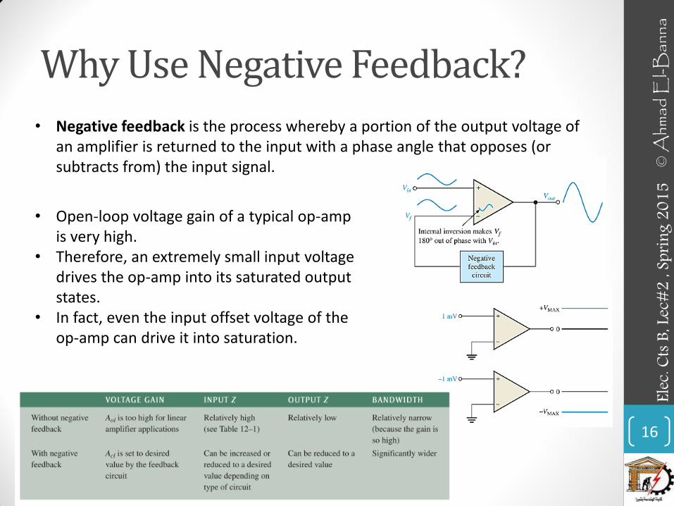
• Negative feedback is the process whereby a portion of the output voltage of an amplifier is returned to the input with a phase angle that opposes (or subtracts from) the input signal.
• Open-loop voltage gain of a typical op-amp is very high.
• Therefore, an extremely small input voltage drives the op-amp into its saturated output states.
• In fact, even the input offset voltage of the op-amp can drive it into saturation.
OP-AMPS WITH NEGATIVE FEEDBACK
17
© A
hmad
El-B
anna
Ele
c. Ct
s B, L
ec#2
, Spr
ing 2
015
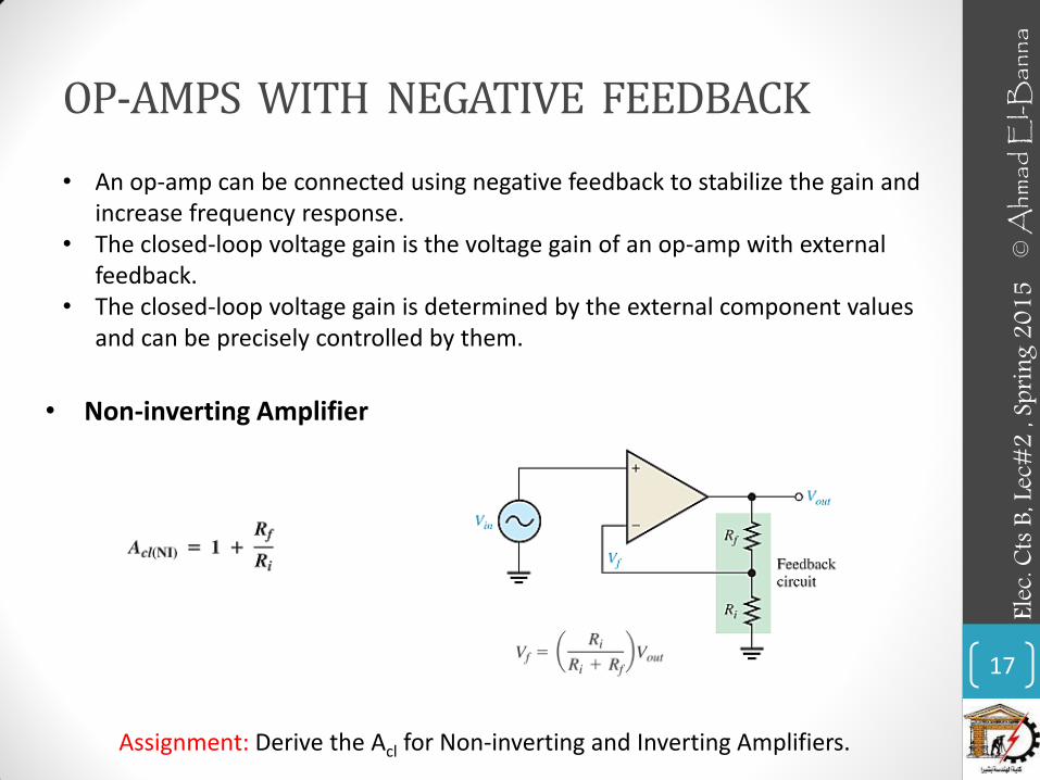
• An op-amp can be connected using negative feedback to stabilize the gain and increase frequency response.
• The closed-loop voltage gain is the voltage gain of an op-amp with external feedback.
• The closed-loop voltage gain is determined by the external component values and can be precisely controlled by them.
• Non-inverting Amplifier
Assignment: Derive the Acl for Non-inverting and Inverting Amplifiers.
OP-AMPS WITH NEGATIVE FEEDBACK..
18
© A
hmad
El-B
anna
Ele
c. Ct
s B, L
ec#2
, Spr
ing 2
015
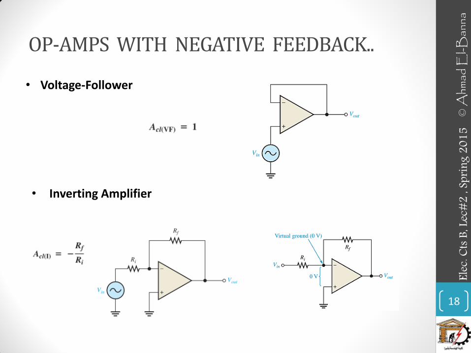
• Inverting Amplifier
• Voltage-Follower
EFFECTS OF NEGATIVE FEEDBACK ON OP-AMP IMPEDANCES
19
© A
hmad
El-B
anna
Ele
c. Ct
s B, L
ec#2
, Spr
ing 2
015
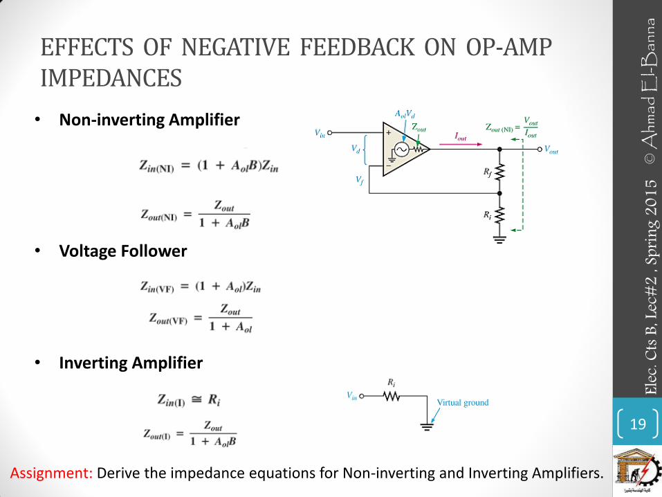
• Non-inverting Amplifier
• Voltage Follower
• Inverting Amplifier
Assignment: Derive the impedance equations for Non-inverting and Inverting Amplifiers.
BIAS CURRENT AND OFFSET VOLTAGE 20
© A
hmad
El-B
anna
Ele
c. Ct
s B, L
ec#2
, Spr
ing 2
015
• Certain deviations from the ideal op-amp must be recognized because of their effects on its operation.
• Transistors within the op-amp must be biased so that they have the correct values of base and collector currents and collector-to-emitter voltages.
• The ideal op-amp has no input current at its terminals; but in fact, the practical op-amp has small input bias currents typically in the nA range.
• Also, small internal imbalances in the transistors effectively produce a small offset voltage between the inputs.
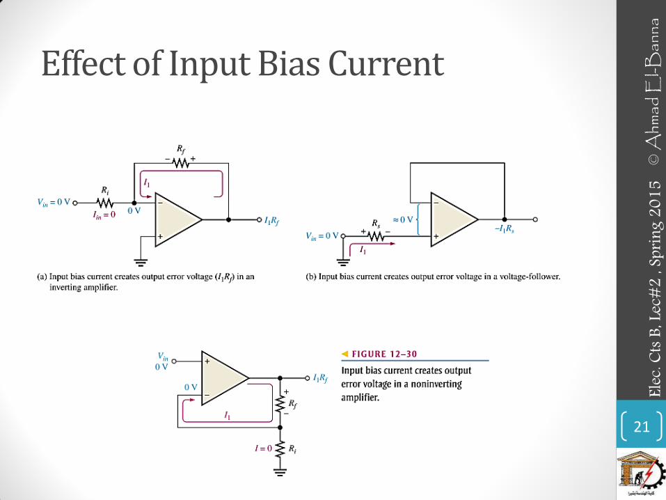
Effect of Input Bias Current
21
© A
hmad
El-B
anna
Ele
c. Ct
s B, L
ec#2
, Spr
ing 2
015
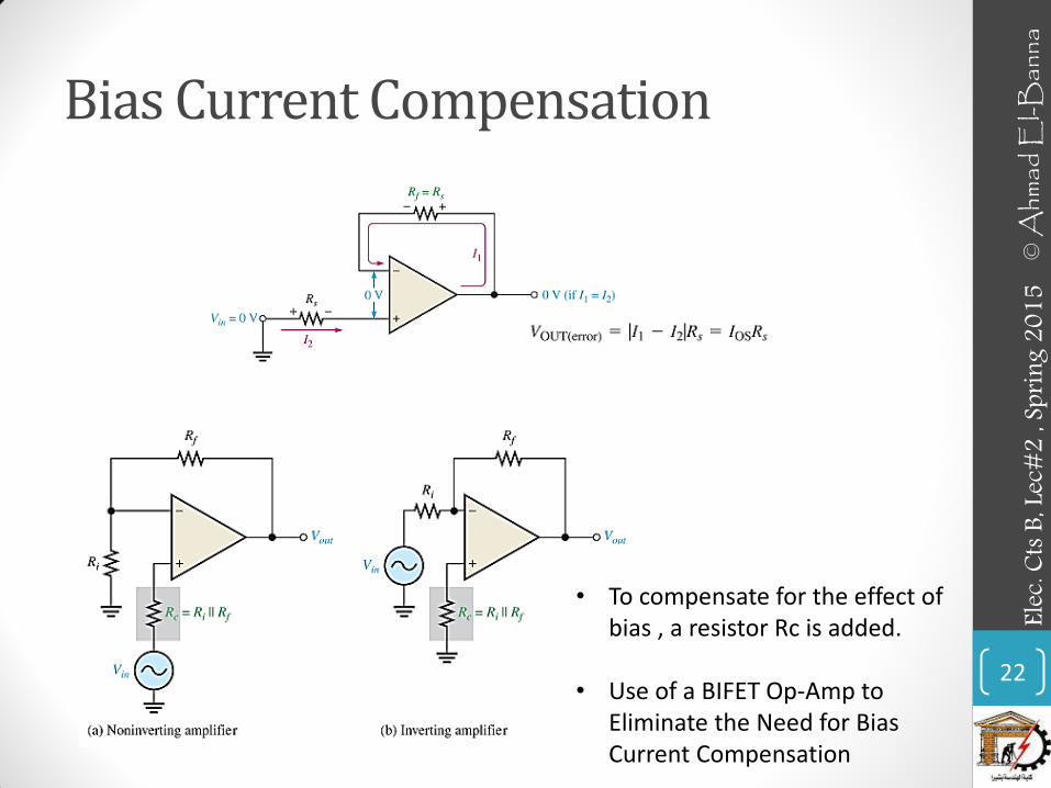
Bias Current Compensation
22
© A
hmad
El-B
anna
Ele
c. Ct
s B, L
ec#2
, Spr
ing 2
015
• To compensate for the effect of bias , a resistor Rc is added.
• Use of a BIFET Op-Amp to Eliminate the Need for Bias Current Compensation
Effect of Input Offset Voltage
23
© A
hmad
El-B
anna
Ele
c. Ct
s B, L
ec#2
, Spr
ing 2
015
Input Offset Voltage Compensation
OPEN & CLOSED LOOP FREQUENCY RESPONSES
24
© A
hmad
El-B
anna
Ele
c. Ct
s B, L
ec#2
, Spr
ing 2
015
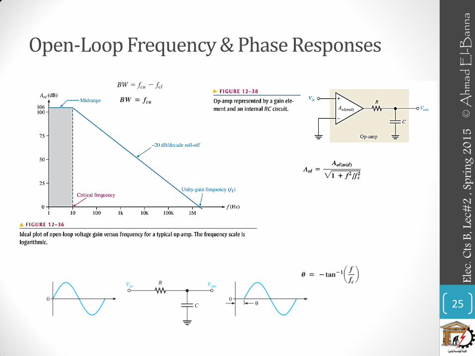
Open-Loop Frequency & Phase Responses
25
© A
hmad
El-B
anna
Ele
c. Ct
s B, L
ec#2
, Spr
ing 2
015
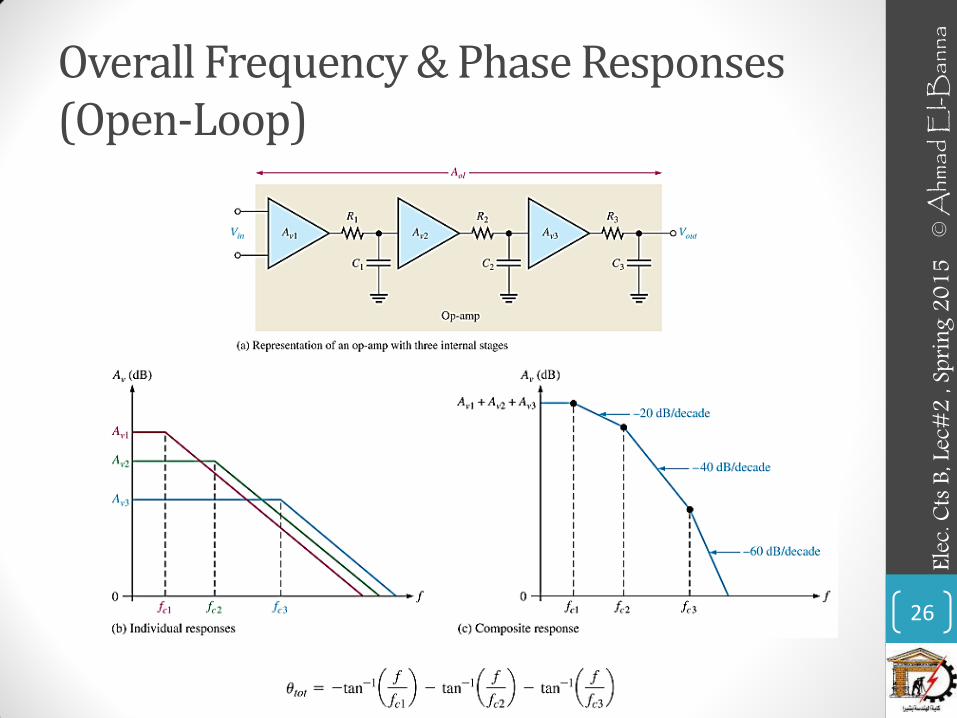
Overall Frequency & Phase Responses (Open-Loop)
26
© A
hmad
El-B
anna
Ele
c. Ct
s B, L
ec#2
, Spr
ing 2
015
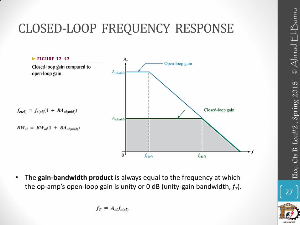
CLOSED-LOOP FREQUENCY RESPONSE
27
© A
hmad
El-B
anna
Ele
c. Ct
s B, L
ec#2
, Spr
ing 2
015
• The gain-bandwidth product is always equal to the frequency at which the op-amp’s open-loop gain is unity or 0 dB (unity-gain bandwidth, fT).
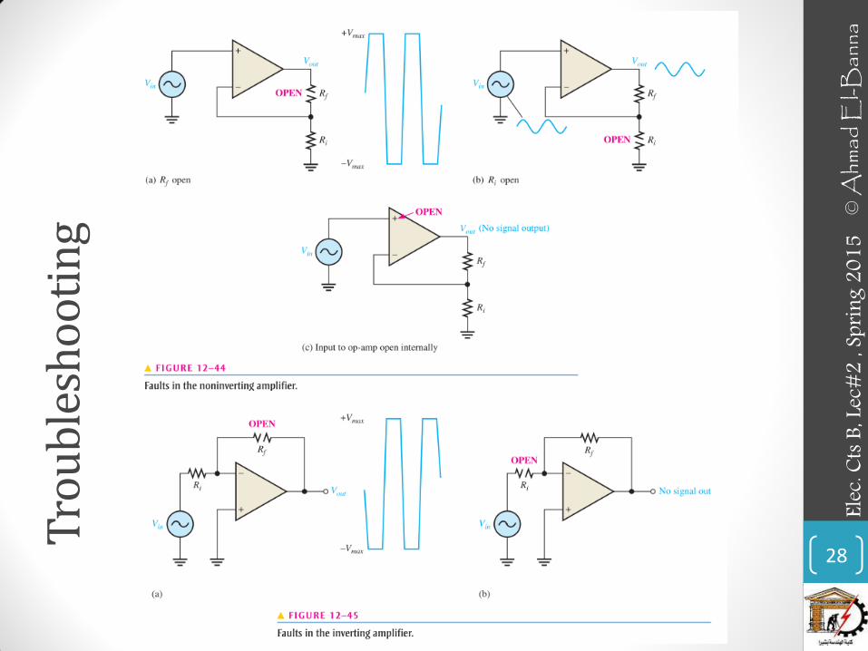
Tro
ub
lesh
oo
tin
g
28
© A
hmad
El-B
anna
Ele
c. Ct
s B, L
ec#2
, Spr
ing 2
015
• For more details, refer to:
• Chapter 12, T. Floyd, Electronic Devices, 9th edition.
• The lecture is available online at:
• http://bu.edu.eg/staff/ahmad.elbanna-courses/12135
• For inquires, send to:
29
© A
hmad
El-B
anna
Ele
c. Ct
s B, L
ec#1
, Spr
ing 2
015