Embed Size (px)
Citation preview
P. Bruschi: Notes on Mixed Signal Design Chap.3, Part 2
1
1 Operational amplifiers.
1.1 Definition and specifications.
The operational amplifier (op-amp) is an amplifier with the following characteristics:
Differential input
Very large DC gain
High input impedance on both inputs
Stability over a wide range of negative feedback conditions.
The op-amp is a very versatile cell that can be used to build feedback loops, which, thanks to the large gain and high input impedance of the amplifier, perform operations showing low sensitivity to the amplifier characteristics.
The operational amplifier shares many of its specifications with generic amplifiers (instrumentation amplifiers, low noise pre-amplifiers, power amplifiers etc.) but there are a few that are specific to this kind of amplifier and are related to the fact that operational amplifiers are designed to be used in closed loop configurations.
In order to understand these specifications, we can focus on the typical closed loop configuration shown in Fig. 1.1 (a). The input signal is indicated with vs, and the output signal is vout. The open loop gain (with open output port) of the amplifier, is indicated with AOL, while the amplifier output impedance is indicated with Zout.; ZL is the load impedance. The figure refers to the small signal equivalent circuit. With such a network, we generally intend to synthesize a transfer function vout/vs that depends only on the transfer functions of the feedback network, defined by the following formulas, referring to the configuration of Fig. 1.1 (b):
00
;
so vo
eN
vs
eN
v
v
v
v (1.1)
If the amplifier is ideal, i.e. its output impedance is zero and its input impedance is infinite, the transfer function turns out to be:
1OLN
OLN
N
N
S
OUT
A
A
v
v (1.2)
P. Bruschi: Notes on Mixed Signal Design Chap.3, Part 2
2
If the gain AOL of the amplifier is high enough to make |NAOL|>>1, then the transfer function can be approximated by
N
N
S
OUT
v
v
(1.3)
In these conditions, the transfer function is set only by the feedback network while the amplifiers provides only the required gain to make this result occur and the required power to drive the load and the feedback network itself. The latter can be designed with only passive components (no power gain is required), that generally provide transfer functions that can be designed to be precise and stable with respect to temperature, process variations and time.
Unfortunately the amplifier is not ideal. While the condition of high input impedance can be generally fulfilled, at least in a restricted frequency range, the output impedance is not negligible in most cases.
Fig. 1.1. An op-amp based closed loop network (a); definitions of the feedback network transfer functions (b)
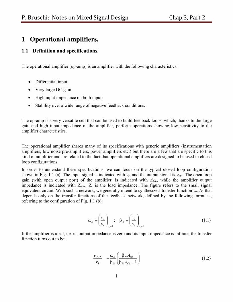
The circuit can be rigorously analyzed using Pellegrini’s cut-insertion theorem [1], cutting the network at the amplifier input as in Fig. 1.2 (a). Since the amplifier can generally be assumed to be unidirectional, then Zp=Zi, where Zi is the input impedance of the amplifier. Considering appendix 3.2, we can write the overall transfer function as:
AA
A
v
v
s
out**
*
*
*
11
(1.4)
where the transfer function * and * are calculated considering the network of Fig.1.2 (b), which differs from Fig. 1.1 (b) only by the presence of the impedance Zp=Zi in parallel to the error port of the feedback network:
P. Bruschi: Notes on Mixed Signal Design Chap.3, Part 2
3
0
*
0
* ;
so vo
r
vs
r
v
v
v
v (1.5)
Note that the higher |Zi,|, the closer * and * are to N and N, respectively.
Fig. 1.2: Application of the cut-insertion theorem to the network of Fig. 1.1 (a); network used to define * and *.
Parameters A and are calculated on the cut network of Fig. 1.2(a) and are given by:
0
0//
//
p
s
vs
out
Lout
L
OL
vp
out
v
v
ZZZ
ZZA
v
vA
: (1.6)
where Z is the impedance seen by voltage source vo in Fig. 1.2 (b) and represents the loading effect of the feedback network on the amplifier output port. Note that, due to the output impedance Zout and the combined loading effect of ZL and Z , |A| is often significantly smaller than |AOL|. If we consider (1.4), we can compute the relative error of the transfer function with respect to the asymptotic one, -*/*, obtained for |A| that tends to infinity.
Ls
outR
AAAAv
v1
11
11
1
1/
**
*
**
*
**
*
*
*
(1.7)
As stated above, the error given by (1.7) measures the relative discrepancy of the real transfer function with respect to the asymptotic function -*/*. However, as it is demonstrated in Appendix 3.2, -*/*
P. Bruschi: Notes on Mixed Signal Design Chap.3, Part 2
4
is exactly equal to -N/N, which is the ideal transfer function, calculated considering only the properties of the feedback network and no loading effects from Zp.
Expression (1.7) shows that the relative error is the of the order of 1/|*A|. For more details on this topics and for a demonstration of (1.4), see Appendix 3.2.
Gain A, resulting from loading the amplifier with the specified load and with the feedback network, should be still high enough to make the relative error, given by (1.7), smaller than the maximum value allowed by the target application. This means that a low output impedance is desirable, but not mandatory for an op-amp. Many integrated operational amplifiers are marked by output resistances (Rout) of the order of several k, or even tens of k. In many applications, the total load resistance is much smaller than Rout, so that |A|<<|AOL|. This does not represent a problem as far as the residual |*A| value is still >>1.
Maximum output current
In the above discussion, we have stated that a low output impedance is not strictly required, provided that the resulting loop gain is still high enough. Dealing with the output impedance, we have implicitly assumed that we are working with small signal circuits. The scheme of Fig. 1.1 (a) implement the ideal transfer function -/ regardless of the value of the load impedance ZL, obviously provided that |ZL| does not get so low that |A| drops below the minimum value for keeping the error R negligible. This is equivalent to say that the closed loop circuit has a very low output impedance independently of the op-amp open loop output impedance. This is a well-known benefit of negative feedback.
The situation can be different if we consider large signals. Due to saturation of one or more stages in the op-amp, the output stage can be unable to feed the current needed to produce the required voltage level in the output load (comprehensive of the feedback network load Z). Then, the real specification that we will be obliged to consider is the maximum current that the output stage can feed to the load. Generally, it is important to take into account both the maximum positive and negative output currents.
The maximum output current affects the maximum output swing (at a certain total load RL) according to the following conditions:
OPLoutONL IRVIR (1.8)
where ION and IOP are the maximum currents (absolute values) that the output port can sink (negative current) or source (positive current), respectively.
A maximum output current can be required also if a pure capacitive load has to be driven. In that case, the currents ION and IOP determine the limits imposed by the output stage on the falling and rising slopes of the output voltage, respectively.
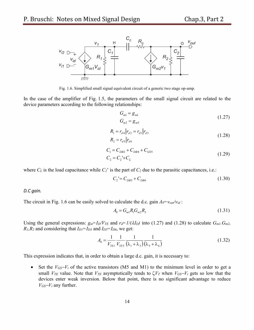
Stability
The stability of an op-amp clearly refers to cases where it is used in closed loop configuration to implement blocks different from oscillators and latches. The important quantity to be taken into consideration is the loop gain A. A general-purpose op-amp should be designed to be stable in a wide variety of negative feedback configurations. A typical requirement is that the amplifier is stable when
P. Bruschi: Notes on Mixed Signal Design Chap.3, Part 2
5
= 1 (conventionally indicated as “unity gain condition”). Figure 1.3 shows a sketch of a possible Bode plot of the A magnitude and phase. In order to have dc stability, since |A|>>1 for the reasons exposed above, A should be negative at zero frequency, that is the phase diagram asymptotically tends to 180° when the frequency tends to zero. Due to the reactive elements present in the circuit (normally capacitances), the phase will decrease as the frequency is progressively increased. At the same time, the magnitude will also decrease. In order to obtain stability, it is important to guarantee that for no frequency the following conditions simultaneously hold:
0
1
A
A (1.9)
In practice, we have to avoid that the phase becomes zero at a frequency where the magnitude has not yet fallen below the zero dB line. The frequency, at which |A|=1 (0 dB), is called the unity gain frequency and is indicated with f0. The residual phase at f=f0 is called phase margin (m). A high phase margin is required to guarantee stability even in the case of large device parameter variations due to temperature and process spread. Large phase margins also reduce unwanted features of the closed loop step response, such as overshoot and ringing. Generally, particular techniques are required to shape the open loop frequency response of an operational amplifier to obtain the behavior of Fig. 1.3 with a sufficient phase margin. These operations are indicated as frequency compensation of the amplifier.
The frequency response of general-purpose op-amps is generally of dominant pole type, as that shown in Fig. 1.3, where the dominant pole frequency is indicated with fp. It should be desirable, when possible, to place all non-dominant singularities beyond f0. In the case of unity gain configuration, shown in Fig. 1.3, || reaches the maximum value achievable with a resistive feedback network, that is ||=1. The corresponding magnitude response of A is shown in Fig. 1.3. If we have to design an amplifier with a gain > 1, the required || will be < 1. In this case, the phase diagram will be unchanged while the magnitude diagram will shift down, as shown in the figure. As a result, f0 will be lower than in the unity gain case and the phase margin increases, improving stability. For this reason, the unity gain condition is generally considered as a worst case in terms of stability requirements.
In the case that only a single non-dominant pole (indicated with f2 in the figure) affects the phase at f0, the phase margin (in radians) will be given by:
0
2
2
0
2
0 arctanarctan2
arctan2 f
f
f
f
f
fm (1.10)
In two stage op-amps, it is often possible to assume that only one non-dominant pole exists. By design, the frequency f2 is set at a value equal to f0, where is a sort of safety factor. A typical value is =3, which, according to Eq. (1.10), provides a phase margin of nearly 72°. Phase margins for various values of are given in Table 1.1.
0.5 1 2 3 5
m 26.6° 45° 63.4° 71.6° 78.7°
P. Bruschi: Notes on Mixed Signal Design Chap.3, Part 2
6
Table 1.1. Phase margin for various =2/0 values.
The effect of singularities at frequencies higher than f2 will usually further reduce the actual phase margin; therefore, this procedure should be used as an approximate method to set the phase margin. More precise estimation and refinement of the phase margin has to be performed by means of an electrical simulator.
Fig. 1.3. Magnitude and phase diagram of the loop gain for only two singularities.
As stated earlier, use of the op-amp in closed loop configurations with |<1 facilitates the achievement of stability. For this consideration, we have assumed that is a real, negative number. Examples of feedback networks that satisfy this property are either all resistor networks or all capacitor networks such those of Fig. 1.4. If an op-amp is designed to be unity gain stable, it will remain stable if used with
|<1. Op-amps for special applications may be designed to be stable for 1 MAX . In this case, it is
not guaranteed that the amplifier is stable in unity gain configuration. If such an op-amp is used in non-inverting configurations, where the closed loop gain is |AV|=|1/|, there will be a minimum gain AVMIN =1/MAX > 1, below which the amplifier may be unstable. For examples, commercial amplifiers such as the Analog Devices OP37 are guaranteed stable for AV > 5.
Speed Specifications.
For an operational amplifier, speed is expressed by two specifications: the Gain-Band-Width product (GBW) and the slew rate. The GBW is a small signal parameter. It is particularly useful if we can consider that the amplifier open loop frequency response is characterized by a single pole, i.e. the open loop gain AOL is given by:
p
OLs
AsA
/1)( 0 (1.11)
where p =2fp and fp is the pole frequency. In this case, if A0>>1, (which is always true for an op-amp), the unity gain frequency f0 is practically equal to A0fp, so that f0 coincides with the GBW. An
P. Bruschi: Notes on Mixed Signal Design Chap.3, Part 2
7
approximate very useful equation that is strictly applicable if fp is the only singularity, but works fine also in the case that fp is the dominant pole, is the expression that gives the upper band limit (-3 db) of an amplifier built connecting an op-amp in closed loop with an all-resistor network:
0V
HA
GBWf (1.12)
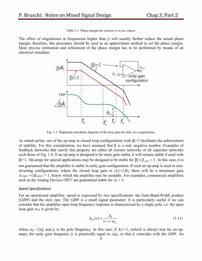
where fH and AV0 are the upper band limit and dc gain of the closed loop amplifier, respectively. Expression (1.12) is valid for the non-inverting amplifier of Fig. 1.1 (b) and can be applied also to the typical inverting amplifiers of Fig. 1.4 (a), substituting AV0 in (1.12) with |AV0|+1. It can be shown that the validity of (1.12) can be extended to all those cases of feedback network characterized by a pure real transfer function () from dc to f0. This is the case of all-capacitors network, such that of Fig. 1.4 (b), which are commonly used in switched capacitors architectures.
Fig. 1.4. Feedback configuration resulting in a pure real transfer function.
The singularities that can be calculated using the GBW are suitable to describe the response to small signals. For example, the time constant, which characterizes an inverting or non-inverting amplifier like those depicted above, is =(2fH)-1. If a step of small amplitude is applied to those amplifiers, the output voltage settles to the finale value after several time constants (e.g. 4.6 for 1 % residual error). However, fH (and thus GBW, from which fH is derived) is not sufficient to calculate the response to signals as large as to saturate the amplifier input stages. In these cases, the amplifier output voltage varies at a fixed rate, which is independent of the input signal.
The maximum rising and falling rate of the output voltage is indicated as slew rate (sR). If we apply a step of large amplitude to an amplifier built using an op-amp in closed loop configuration, the response is initially a ramp with a slope equal to the sR. This slope is smaller (even much smaller in the case of very large steps) than it would result from a the pure linear response. When the output voltage gets close to the final value, the input stages exit from saturation and the response is linear again, so that an exponential approach begins. In the case of very large steps, most of the settling time is spent with the amplifier in slew rate, so that the settling time itself can be approximated by Vout / sR. where Vout is the amplitude of the output step.
In the particular case of sinusoidal input, the slew rate produces a distortion of the output voltage that begins to show at the points of maximum derivative, i.e. at the instants where the sinusoid crosses the

P. Bruschi: Notes on Mixed Signal Design Chap.3, Part 2
8
zero value. The maximum undistorted output amplitude allowed to a sinusoid of frequency f is given by:
f
sV R
M
2
max (1.13)
If the amplitude is much higher than the limit given by (1.13), the output voltage approximates a triangular waveform.
To summarize, a reasonably complete set of specifications for a CMOS operational amplifier is the following:
DC gain A0
Speed: Gain-Band-Width product (GBW) and Slew rate (sR)
Closed loop stability: e.g. phase margin in unity gain configuration and particular load conditions (typically a maximum load capacitance CL is specified)
Input referred voltage noise: Thermal noise density: SvT, Flicker noise: kF=fSvF(f)
Offset (Input offset voltage: io)
Static power consumption (Isupply, minimum Vdd)
Maximum output current (positive and negative)
Ranges: Input common mode range (CMR), output swing.
Common mode rejection ratio (CMRR) and power supply rejection ratio (PSRR).
P. Bruschi: Notes on Mixed Signal Design Chap.3, Part 2
9
1.2 Operational amplifier design: general considerations.
As for other analog circuits, the design of an operational amplifier can be divided into two well distinct steps:
1. choice of the topology;
2. device sizing.
For the first step, it can be useful to consider a small set of different topologies, which can efficiently satisfy the most common requirements. It is a good idea to start from the simplest circuit and then increase its complexity only if the specifications cannot be met. The most important parameter that discriminates operational amplifier topologies is the number of stages. For an operational amplifier, the stages to be counted are only the gain stages. The following considerations about the number of stages can be drawn:
Single stage amplifiers are characterized by only one high resistance node. The dominant pole will be associated to that node. Frequency compensation can be achieved by simply connecting a capacitor between the high impedance node and ground, lowering the pole frequency and, consequently, the unity-gain frequency f0. If the high impedance node is the output node, the amplifiers are indicated also as OTAs (Operational Transconductance Amplifiers). Relatively high voltage gains (up to 80 dB) can be obtained with single-stage cascode OTAs. However, their application is limited only to op-amp intended to drive capacitive loads, since the high gain relies on the high output resistance that vanishes when resistive loads are applied. Application of source follower stages between the high impedance node and the output port may eliminate this problem, but its use is discouraged due to the output swing penalty introduced by these stages.
Two-stage op-amps are characterized by two high impedance nodes. For the same reasons of OTAs, source-follower output stages are seldom used, so that the high impedance node of the second stage coincides with the output port. With non-cascode two-stage amplifiers, it is possible to obtain the same gains of cascode OTAs but without the necessity of an extremely high output resistance. Much higher gains can be obtained by using a cascode first stage. In this way, it is only the internal high resistance node to be boosted, with no effect on the output resistance. Open loop gains up to 120 dB can be reached with two-stage op-amps. Frequency compensation of two-stage op-amps is generally accomplished through Miller compensation.
Three or more stage op-amps are necessary when the required gain cannot be achieved with two-stage architectures. This occurs when MOSFETs with sub-micron lengths are used, for example to achieve very high GBWs. Short lengths increase the MOSFET , reducing the device output resistances. Low supply voltages, preventing the use of cascode stages, contribute to reduce the maximum gain available with two-stage op-amps, increasing the demand for multiple stage amplifiers. Compensation is more critical in multiple stage amplifiers. Nested Miller schemes are often adopted.
P. Bruschi: Notes on Mixed Signal Design Chap.3, Part 2
10
In the next part of this chapter, we will focus on two stage amplifiers, which still represent the mostly used op-amp category.
1.3 Operational amplifier design: two stage operational amplifiers
We will analyze the basic two-stage CMOS op-amp, for which we will describe a relatively simple sizing strategy, aimed at satisfying important specifications.
The simplest two-stage CMOS operational amplifier is shown in Fig. 1.5, where the two high resistance nodes are indicated with H and O. The circuit is biased by M8, which will be omitted in next figures. The bias voltage VBIAS, produced by M8, drives M7 and M6 current sources, providing the bias currents of the first and second stage, respectively. The group RC-CC is introduced to perform frequency compensation. We have considered that the amplifier is powered by a single supply voltage Vdd. In the case of dual power supply, gnd should be replaced with VSS <0.
Fig. 1.5. The simplest two-stage CMOS operational amplifier
Degrees Of Freedom
Sizing is the operation by which the device parameters (e.g. width / length for MOSFETs) and bias are chosen in order to obtain the required performances. Not all parameters are independent, so that it is possible to find a restricted set of values, from which all the others can be derived. Parameters in this set are called Degrees Of Freedom (DOFs). Clearly, there is not a single set of possible DOFs for a circuit but the choice of a proper DOF-set facilitates the sizing operation. If we exclude M8, which can
P. Bruschi: Notes on Mixed Signal Design Chap.3, Part 2
11
be considered an external element of the cell (a single device can provide VBIAS to several op-amps), the circuit has five independent MOSFETs (M1=M2 and M3=M4) and two passive elements (RC, CC). Considering that each MOSFET introduces two parameters (W, L), we have an initial set of 12 DOFS (including CC and RC), to which I0 has to be added. Note that I1 = I06/7, thus it is not a free parameter. The total DOFS are then 13. We can start considering only the DOFs that affect the operating point, neglecting for now the compensation network. The resulting set of 11 DOFs can be further reduced introducing a few relationships that will be explained in the following paragraph.
Static equations
-) Null systematic offset. In the nominal design, we usually require that for null input differential voltage (Vid=0), the output voltage is zero. Since no random mismatch errors are present in the nominal design, deviation from this condition means that a systematic offset is present. In a single power supply circuit, the conventional zero voltage for signals cannot coincide with the gnd potential, otherwise negative signals could not be represented, being the output node prevented from getting lower than the lowest power supply rail (i.e. gnd). We generally specify an intermediate point between Vdd and gnd as the signal zero level. A typical choice fro the zero level is Vdd/2, but also other solutions are possible. In same cases, the zero level is chosen to suit the input range of the stage that follows the op-amp. Note that it is not possible to precisely determine the output voltage of the op-amp of Fig. 1.5. The reason is that M5 and M6 behave as two opposed current sources and, if both are in saturation region, the resulting voltage strongly depends on the effect of VDS on the drain current, effect that is not precisely predictable. We can impose a much simpler relationship regarding the output short-circuit current instead of the output voltage. If we short-circuit the output port by connecting it to a voltage source equal to the required zero level (e.g. Vdd/2), which should keep both M5 and M6 in saturation, the short circuit current will be:
65 DDSCout III (1.14)
Considering all MOSFETs in saturation region, the current ID6 is given by:
0
7
66 IID
(1.15)
For zero input differential voltage, currents and voltages in the input stage are symmetrical. Current I0 is then split into two equal parts flowing through the M1 and M2 branch. Furthermore, in these conditions, points K and H in Fig. 1.5 are at the same potential. As a result, M5 and M3 has the same VGS (remember that this condition occurs only for null differential voltage) and the current ID5 can be written as:
20
3
55
IID
(1.16)
Substituting ID6 and ID5 from (1.15) and (1.16) into (1.14) and imposing Iout-SC=0, we get a condition for the betas:
P. Bruschi: Notes on Mixed Signal Design Chap.3, Part 2
12
3
5
7
6
2
1
(1.17)
Note that a small Iout-SC is able to produce large output voltage variations, due to the relatively high output resistance (equal to the parallel of rd5 and rd6). Even Iout-SC values of a few percent of the MOSFET quiescent drain currents can produce output voltage variations as large as to push either M5 or M6 into triode region (saturation of the output voltage).
-) Symmetrical output swing. The output voltage can approach the gnd and Vdd rails, but should maintain a distance from them equal to M5 and M6 saturation voltage, in order to prevent them from getting into triode region. The output swing will then be given by:
65 tGSddOUTtGS VVVVVV (1.18)
The output swing is symmetrical if the minimum distances from the gnd and Vdd rails are identical. This condition can be useful for general-purpose op-amps and is obtained imposing:
65 tGStGS VVVV (1.19)
-) Precise current mirroring. Condition (1.17) is based on the assumption that ID6/ID7 and ID5/ID3 current ratios coincides with the respective beta ratios. This clearly requires that the threshold voltages of the MOSFETs involved in the ratios are equal. Considerable differences in the threshold voltages can be caused by using device with different lengths. Note that errors in the current ratios in (1.17) may introduce a non-negligible output short circuit current, which would introduce a systematic offset. This problem can be mitigated by imposing:
76 LL (1.20)
53 LL (1.21)
Choice of the static DOF set
Reducing the number of DOFs may significantly simplify amplifier sizing. Every additional equation reduces the DOFs by one unit. Equations regarding the DOFs are called “equality constraints”. This distinguishes equations from “inequality constraints”, consisting in inequalities generally related to amplifier specifications (e.g. GBW > 10 MHz). Starting from the initial set of 11 static DOFs, if we consider equations (1.17), (1.19), (1.20), and (1.21) we reduce the DOFs to only 7 parameters. We will follow this approach in the next part of this chapter. However, it should be observed that only (1.17) is strictly mandatory. Adopting also the other three conditions, might results in design limitations that completely counterbalance the advantages deriving from precise mirroring and symmetrical output swing. In these cases, the designer can selectively remove one or more arbitrary constraint and estimate the possible negative effect using proper simulation tools.
As we have stated earlier, there are several equivalent way to choose the residual 7 DOFs. A possible criterion, followed in the rest of this chapter, is that of assigning as much as possible DOFs to the device that perform the main operations. In the circuit of Fig. 1.5 these devices are the active
P. Bruschi: Notes on Mixed Signal Design Chap.3, Part 2
13
MOSFETs of the first and second stage, i.e. M1 (together with M2) and M5. To define M1 and M5 completely, we have decided to include their dimensions (W and L) and the overdrive voltage (VGS-Vt) into the DOF set. In this way also M1 and M5 operating point is fixed. To reach the total number of 7 (static) DOFs, L6 has also been included into the DOF set. The complete set of static DOFs is then:
6555111 ,)(,,,,, LVVLWVVLWDOFs tGStGS (1.22)
From these DOFs, it is possible to derive all the other static circuit parameters. We will refer to the case of all devices in strong inversion, but extension to the case of moderate/weak inversion is possible by using the respective equations of the current in place of the square-law approximation used here. First, note that M1 and M5 currents are known, being given by:
25
5
55
2
11
11
22tGS
OXnDtGS
OXp
D VVL
WCIVV
L
WCI
(1.23)
Device M3 is then completely determined by:
OXntGS
DDDtGStGS
C
L
VV
IWIILLVVVV
3
2
3
33135353
2,,)()( (1.24)
As far as M6 is concerned its length L6 belongs to the DOFs. The other parameters can be obtained adding condition (1.19) and considering that ID6=ID5:
5 6 5 5 66( ) ,GS t GS t D DV V V V I I (1.25)
Finally, M7 is completely determined considering that, using (1.20):
176767 2,,)()( DDtGStGS IILLVVVV (1.26)
Small signal equivalent circuit
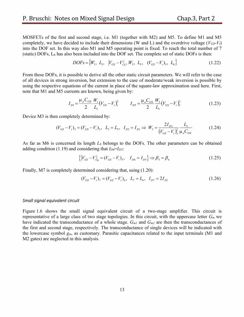
Figure 1.6 shows the small signal equivalent circuit of a two-stage amplifier. This circuit is representative of a large class of two stage topologies. In this circuit, with the uppercase letter Gm we have indicated the transconductance of a whole stage. Gm1 and Gm2 are then the transconductances of the first and second stage, respectively. The transconductance of single devices will be indicated with the lowercase symbol gm, as customary. Parasitic capacitances related to the input terminals (M1 and M2 gates) are neglected in this analysis.
P. Bruschi: Notes on Mixed Signal Design Chap.3, Part 2
14
Fig. 1.6. Simplified small signal equivalent circuit of a generic two stage op-amp.
In the case of the amplifier of Fig. 1.5, the parameters of the small signal circuit are related to the device parameters according to the following relationships:
52
11
mm
mm
gG
gG
(1.27)
652
31241
dd
dddd
rrR
rrrrR
(1.28)
L
GSDBDB
CCC
CCCC
'22
5421 (1.29)
where CL is the load capacitance while C2’ is the part of C2 due to the parasitic capacitances, i.e.:
652 ' DBDB CCC (1.30)
D.C gain.
The circuit in Fig. 1.6 can be easily solved to calculate the d.c. gain A0=vout/vid :
22110 RGRGA mm (1.31)
Using the general expressions: gm=ID/VTE and rd=1/(ID) into (1.27) and (1.28) to calculate Gm1.Gm2, R1,R2 and considering that ID1=ID3 and ID5=ID6, we get:
653151
0
1111
TETE VVA (1.32)
This expression indicates that, in order to obtain a large d.c. gain, it is necessary to:
Set the VGSVt of the active transistors (M5 and M1) to the minimum level in order to get a small VTE value. Note that VTE asymptotically tends to VT when VGSVt gets so low that the devices enter weak inversion. Below that point, there is no significant advantage to reduce VGSVt any further.
P. Bruschi: Notes on Mixed Signal Design Chap.3, Part 2
15
Use device lengths considerably greater than the minimum value, since the lambda parameters increase as the channel lengths are reduced.
Frequency response
Solution of the small signal circuit of Fig. 1.6 in the s domain gives three poles at angular frequencies p, 2, 3, and one zero sz. Approximate expressions of these singularities are the following [2]:
1 2 2
1 1
22
1 2 1 2
1
3 3
3 1 2
2
1
1 11 where
1 1 1 1where
1
1
p
m c
m SS
c
S
c S c
z
c c
m
R G R C
G CC
C C C C C
CR C C C C
s
C RG
(1.33)
Note that CS is the series of C1 and C2, while CS3 is the series of all three capacitors present in Fig. 1.6. The approximations used to obtain expressions (1.33) are valid if p<<2. i.e when p is really a dominant pole. This condition is automatically verified, provided that Cc is of the same order of the other capacitors (C1 and C2), R1 and R2 are of the same order of magnitude and Gm2R2>>1. Note that all these conditions are generally valid in all practical two-stage op-amps. The zero sz may be positive, and this has unfavorable consequences on the phase margin, since it adds phase delay to the unavoidable contribution of the poles. The zero is certainly positive if RC is zero. Choosing a proper value for RC it is possible to eliminate the zero or make it negative.
Considering that the frequency response is dominated by p up to the unity gain frequency (0), the latter is then given by:
c
mp
C
GA 1
00 (1.34)
Therefore, the gain bandwidth product will be given by
20
0fGBW (1.35)
Design for GBW and stability
Stability in closed loop configuration is the main aspect of op-amp design since it has to be guaranteed independently from other performances. As we have seen in previous paragraphs, stability is closely related to the GBW. Nevertheless, even if we are designing an op-amp to be used only for d.c. signals,
P. Bruschi: Notes on Mixed Signal Design Chap.3, Part 2
16
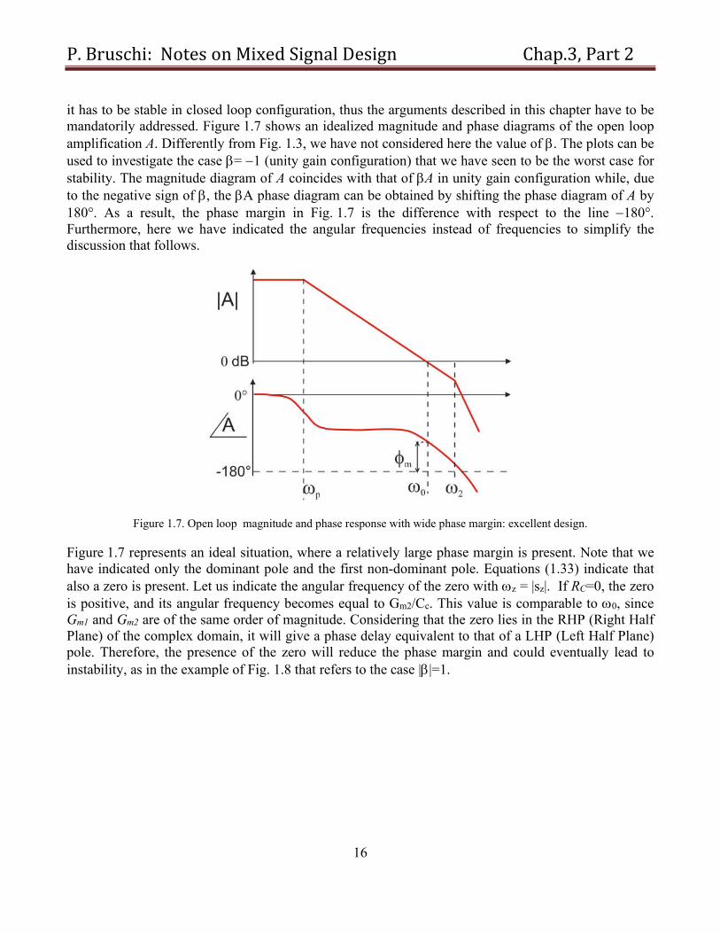
it has to be stable in closed loop configuration, thus the arguments described in this chapter have to be mandatorily addressed. Figure 1.7 shows an idealized magnitude and phase diagrams of the open loop amplification A. Differently from Fig. 1.3, we have not considered here the value of . The plots can be used to investigate the case = 1 (unity gain configuration) that we have seen to be the worst case for stability. The magnitude diagram of A coincides with that of A in unity gain configuration while, due to the negative sign of , the A phase diagram can be obtained by shifting the phase diagram of A by 180°. As a result, the phase margin in Fig. 1.7 is the difference with respect to the line 180°. Furthermore, here we have indicated the angular frequencies instead of frequencies to simplify the discussion that follows.
Figure 1.7. Open loop magnitude and phase response with wide phase margin: excellent design.
Figure 1.7 represents an ideal situation, where a relatively large phase margin is present. Note that we have indicated only the dominant pole and the first non-dominant pole. Equations (1.33) indicate that also a zero is present. Let us indicate the angular frequency of the zero with z = |sz|. If RC=0, the zero is positive, and its angular frequency becomes equal to Gm2/Cc. This value is comparable to 0, since Gm1 and Gm2 are of the same order of magnitude. Considering that the zero lies in the RHP (Right Half Plane) of the complex domain, it will give a phase delay equivalent to that of a LHP (Left Half Plane) pole. Therefore, the presence of the zero will reduce the phase margin and could eventually lead to instability, as in the example of Fig. 1.8 that refers to the case ||=1.
P. Bruschi: Notes on Mixed Signal Design Chap.3, Part 2
17
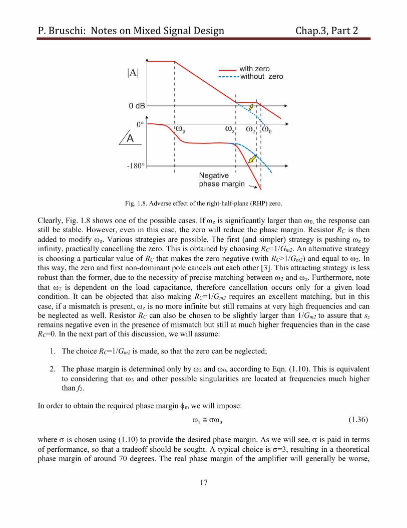
Fig. 1.8. Adverse effect of the right-half-plane (RHP) zero.
Clearly, Fig. 1.8 shows one of the possible cases. If z is significantly larger than 0, the response can still be stable. However, even in this case, the zero will reduce the phase margin. Resistor RC is then added to modify z. Various strategies are possible. The first (and simpler) strategy is pushing z to infinity, practically cancelling the zero. This is obtained by choosing RC=1/Gm2. An alternative strategy is choosing a particular value of RC that makes the zero negative (with RC>1/Gm2) and equal to 2. In this way, the zero and first non-dominant pole cancels out each other [3]. This attracting strategy is less robust than the former, due to the necessity of precise matching between 2 and z. Furthermore, note that 2 is dependent on the load capacitance, therefore cancellation occurs only for a given load condition. It can be objected that also making RC=1/Gm2 requires an excellent matching, but in this case, if a mismatch is present, z is no more infinite but still remains at very high frequencies and can be neglected as well. Resistor RC can also be chosen to be slightly larger than 1/Gm2 to assure that sz remains negative even in the presence of mismatch but still at much higher frequencies than in the case RC=0. In the next part of this discussion, we will assume:
1. The choice RC=1/Gm2 is made, so that the zero can be neglected;
2. The phase margin is determined only by 2 and 0, according to Eqn. (1.10). This is equivalent to considering that 3 and other possible singularities are located at frequencies much higher than f2.
In order to obtain the required phase margin m we will impose:
02 (1.36)
where is chosen using (1.10) to provide the desired phase margin. As we will see, is paid in terms of performance, so that a tradeoff should be sought. A typical choice is=3, resulting in a theoretical phase margin of around 70 degrees. The real phase margin of the amplifier will generally be worse,
P. Bruschi: Notes on Mixed Signal Design Chap.3, Part 2
18
owing to the contribution of other singularities that we are neglecting in this simplified analysis. For this reason, it is necessary to aim at phase margin significantly higher than the real target value.
By substituting the expressions of 2 and 0, given in (1.33) and (1.34), into (1.36), one could calculate the value of the compensation capacitor [4]:
211
221
2
1 411)(
2 CC
C
G
GCC
G
GC S
m
m
m
mc (1.37)
In this way, Cc is no more a DOF, since it can be expressed in terms of the 7 static DOFs. Indeed, Gm1, Gm2 and C1, C2 are actually functions of the DOFs indicated in (1.22). Since also RC has been eliminated from the DOFs with the choice RC=1/Gm2, the only remaining DOFs are those specified in (1.22). Furthermore, this expression could be put into (1.34) and (1.35) in order to calculate the GBW as a function of the DOFs. In practice, this does not lead to equations that can be used to perform manual design of the amplifier, since too many DOFs still appear in (1.37).
It is then necessary to introduce approximations aimed at simplifying the analysis and provide clear indications to the designer. We will then introduce two hypotheses that have to be always checked at the end of the design work:
Hyp. 1 CCCC ,21 (1.38)
Hyp. 2 LCC '2 (1.39)
In practice, hypotheses 1 and 2 means that the parasitic capacitances C1 and C2’ are negligible with respect to the load and compensation capacitances. Hypothesis 1 can be used to simplify the expression of 2 given in Eqns.(1.33). If C1<<C2, then the series capacitance CS is nearly equal to C1. Using hypothesis 1 again, C1<<CC, thus we can write:
2
2
21
22
C
G
CC
G mm
(1.40)
Using Hyp.2, we can finally write:
L
m
C
G 22 (1.41)
Now, using (1.35) and stability condition (1.36), we can write a useful expression of the GBW:
L
m
C
GGBW
22
2
1
2
1 (1.42)
Equation (1.42) states that, to obtain a given GBW, it is necessary to start designing the output stage. This seems in contrast with (1.34) and (1.35), which relate the GBW to parameters of the first stage (Gm1) and the compensation capacitor. Actually, (1.34) and (1.35) are correct for the analysis of the amplifier, but not immediately useful during the synthesis. In fact, 0 is not a free parameter but, once
P. Bruschi: Notes on Mixed Signal Design Chap.3, Part 2
19
the phase margin has been chosen, it cannot be larger than 2/. Thus, in order to obtain a certain value of 0, we have to “make room to it” by setting 2. If Hyp.1 and Hyp.2 are valid, 2 depends only on parameters of the output stage and this explains Eq. (1.42).
We can further transform (1.42) to highlight the role of the various DOFs involved. Considering that, for the amplifier of Fig. 1.5, Gm2=gm5, we have:
5
5
2
1
TE
D
L V
I
CGBW
(1.43)
Equation (1.43) directly relates the GBW to the current consumption of the output stage. A high GBW is paid mainly in terms of current consumption. Once the target GWB has been fixed, it is possible to choose a small (VGS-Vt)5 value in order to reduce VTE5 and then obtain the GBW with an as small as possible current consumption. Unfortunately, this condition can be in contrast with other constraints, as it will be shown in the section regarding offset and noise. In next part of this paragraph we will show also that a small (VGS-Vt)5 may lead to violate Hyp. 1 and 2.
Equation (1.43) seems to indicate that there is no upper limit to the GBW, the problem being only power consumption. Furthermore, this equation is independent of process parameters. This is true until Hyp.1 and 2 are valid. To understand what happens when Hyp. 1 and 2 are not applicable, let us consider the expression of ID5, referred to strong inversion operation, for simplicity:
2
2
5
5
55
tGSOXnD
VV
L
WCI
(1.44)
In order to increase ID5 with fixed VGSVt and L, it is necessary to increase W5. This produces an increase of the parasitic capacitances of M5 and, in particular, CDB5 and CGS5. According to Eqns.(1.29), these two capacitances appears in the expression of C1 and C2’, respectively. Therefore, there will be a value of ID5, over which the hypotheses will not hold any more and Eqn. (1.42) cannot be applied any more. It can be useful to rewrite (1.40) without the approximations given by Hyp.1, and 2. The only exception will be the approximation CS/CC<<1, which will be considered to be still valid, since CC can be properly chosen high enough to make this happen. Using the strong inversion approximation for Gm2=gm5, we get:
LCJox
tGSOXn
L
m
CWWLCLWC
VVL
WC
CCC
GGBW
6555
55
5
21
2
3/22
1
'2
1 (1.45)
Parameters CJ and LC are the junction capacitance per unit area and the minimum length of the drain/source diffusion, respectively. Both LC and CJ have been assumed identical for p-MOS and n-MOS devices, for simplicity. Dividing both the numerator and denominator in (1.45) by W5, we get the following expression:
P. Bruschi: Notes on Mixed Signal Design Chap.3, Part 2
20
55
65
5
5
13/22
1
W
C
W
WLCLC
L
VVC
GBWL
CJOX
tGSOXn
(1.46)
The ratio W6/W5 in (1.46) can be regarded as a constant term, since an increase of W5 should be followed by an identical increase of W6 to maintain 6=5, imposed by Eqn. (1.25).
If ID5 is increased to obtain a large GBW, according to Eqn. (1.43), W5 should be increased as well. Eqn. (1.46) shows that the GBW does not increase indefinitely, but tends to an asymptotic value given by:
5
65
5
5
13
22
1*
W
WLCLC
L
VVC
GBW
CJox
tGSOXn
(1.47)
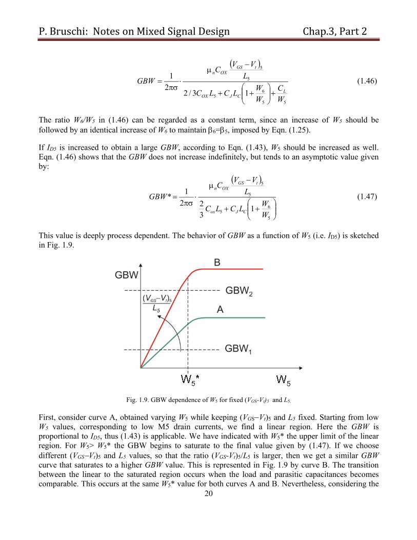
This value is deeply process dependent. The behavior of GBW as a function of W5 (i.e. ID5) is sketched in Fig. 1.9.
Fig. 1.9. GBW dependence of W5 for fixed (VGS-Vt)5 and L5.
First, consider curve A, obtained varying W5 while keeping (VGSVt)5 and L5 fixed. Starting from low W5 values, corresponding to low M5 drain currents, we find a linear region. Here the GBW is proportional to ID5, thus (1.43) is applicable. We have indicated with W5* the upper limit of the linear region. For W5> W5* the GBW begins to saturate to the final value given by (1.47). If we choose different (VGSVt)5 and L5 values, so that the ratio (VGS-Vt)5/L5 is larger, then we get a similar GBW curve that saturates to a higher GBW value. This is represented in Fig. 1.9 by curve B. The transition between the linear to the saturated region occurs when the load and parasitic capacitances becomes comparable. This occurs at the same W5* value for both curves A and B. Nevertheless, considering the
P. Bruschi: Notes on Mixed Signal Design Chap.3, Part 2
21
drain current expression given by (1.44), the value of ID5 for which the linear relationship holds is higher for curve B.
It is interesting to consider two different design cases where we will assume that the length L5 is fixed while (VGS-Vt)5 is a free parameter (i.e. it is not fixed by other specifications), Referring to Fig. 1.9, in the first case the required GBW is indicated by the value GBW1. We note that both curves A and B satisfy the specification with W5 in the linear zone, then (1.43) is valid. In this case, it is convenient to choose curve A, since the (VGSVt)5 is smaller and, from (1.43) the power consumption (due to ID5) is lower. In the second case, it is required to reach GBW2. This value cannot be achieved with curve A and the designer should use a larger (VGSVt)5 and, from (1.43), a larger power consumption. Clearly, for a given process and power supply voltage, there will be a maximum GBW that cannot be exceeded. The continuous improvement of CMOS processes, manly aimed at scaling down the minimum channel length, has produced a corresponding increase in the maximum achievable GBW. In the following part of this discussion, we will assume that Hyp.1 and 2 are valid, so Eqn. (1.41) holds.
Once the value of Gm2 has been determined, it is necessary to calculate the value of the compensation capacitor CC and of the first stage transconductance Gm1.
Going back to the expressions of 0 and 2, given by Eqns. (1.34) and (1.41), respectively, and combining them with the stability condition (1.36), we find:
C
m
L
m
C
G
C
G 12 , (1.48)
from which we obtain CC:
L
m
mC C
G
GC
2
1 (1.49)
In order to calculate CC the designer has to decide the value to assign to Gm1/Gm2. The parameter to be considered is the value of CL. It is possible to start from a commonly used rule of thumb that assigns:
Rule of thumb:
LC
m
m
CC
G
G
1
2
1
(1.50)
Since generally ~3, this means Gm1=Gm2/3. The rule of thumb has the advantage of being simple and making easier to satisfy Hyp. 1, because if CC=CL then:
11 alsothenif CCCC CL (1.51)
The rule of thumb is no more convenient if CL is so large that CC occupies too much silicon area. Note that the amplifier can be designed to drive loads that are external to the chip, so that CL may be relatively large, even up to a few nF. In these cases, it can be convenient to choose smaller Gm1/Gm2 ratios in order to reduce CC. For example, we can choose:
P. Bruschi: Notes on Mixed Signal Design Chap.3, Part 2
22
LC
m
m
CC
G
G
5
1
5
1
2
1
(1.52)
It should be observed that there is no risk that CC becomes too small to satisfy Hyp.1, since we have assumed that CL is particularly large.
Finally, it is important to consider what happens if we have designed an op-amp for a certain CL value and the same op-amp is used with a smaller CL. Note that CL is generally a maximum load capacitance specification, thus the amplifier has to remain stable in closed loop conditions even if CL is completely removed. Let us consider the consequences of reducing CL (or completely removing it) with respect to the value used to design the amplifier:
The unity gain angular frequency 0 does not change, since it is given by (1.34) where CL is not present.
The first non-dominant pole 2 is affected by CL since it is included into C2. Reducing CL will probably lead to violate Hyp.1 and Hyp.2. Therefore, the expression of 2 given in (1.33) should be used. Reducing C2, reduces also CS. Thus, 2 shifts to higher frequencies for two concurrent reasons: (i) denominator (C1+C2) decreases and (ii) also the ratio CS/CC decreases.
For these reasons, if we reduce CL with respect to the specified value, the ratio 2/0 increases and so does the phase margin. On the contrary, if we increase the value of CL over the value used to design the amplifier, the phase margin will progressively decrease and will eventually get negative, resulting in unstable closed loop configurations. This situation is common to most two-stage amplifiers.
Relationship between GBW and slew rate
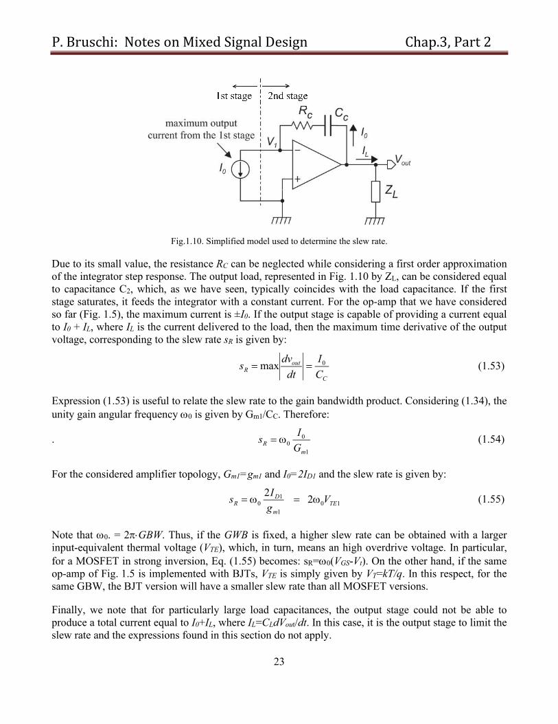
The slew rate is the maximum rate by which the amplifier output voltage can increase and decrease. The effect occurs when one of the amplifier stage saturates and its current reaches the maximum value. In a two-stage op-amp, slew rate is generally due to saturation of the input stage. As Fig. 1.10 shows, the combination of the amplifier second stage (inverting) and compensation capacitor forms a Miller integrator having the output current of the first stage as its input. It can be demonstrated that this schematization is valid for frequencies much higher than the dominant pole fp.
P. Bruschi: Notes on Mixed Signal Design Chap.3, Part 2
23
Fig.1.10. Simplified model used to determine the slew rate.
Due to its small value, the resistance RC can be neglected while considering a first order approximation of the integrator step response. The output load, represented in Fig. 1.10 by ZL, can be considered equal to capacitance C2, which, as we have seen, typically coincides with the load capacitance. If the first stage saturates, it feeds the integrator with a constant current. For the op-amp that we have considered so far (Fig. 1.5), the maximum current is ±I0. If the output stage is capable of providing a current equal to I0 + IL, where IL is the current delivered to the load, then the maximum time derivative of the output voltage, corresponding to the slew rate sR is given by:
C
outR
C
I
dt
dvs 0max (1.53)
Expression (1.53) is useful to relate the slew rate to the gain bandwidth product. Considering (1.34), the unity gain angular frequency 0 is given by Gm1/CC. Therefore:
. 1
00
m
RG
Is (1.54)
For the considered amplifier topology, Gm1=gm1 and I0=2ID1 and the slew rate is given by:
10
1
10 2
2TE
m
DR V
g
Is (1.55)
Note that 0. = 2GBW. Thus, if the GWB is fixed, a higher slew rate can be obtained with a larger input-equivalent thermal voltage (VTE), which, in turn, means an high overdrive voltage. In particular, for a MOSFET in strong inversion, Eq. (1.55) becomes: sR=0(VGS-Vt). On the other hand, if the same op-amp of Fig. 1.5 is implemented with BJTs, VTE is simply given by VT=kT/q. In this respect, for the same GBW, the BJT version will have a smaller slew rate than all MOSFET versions.
Finally, we note that for particularly large load capacitances, the output stage could not be able to produce a total current equal to I0+IL, where IL=CLdVout/dt. In this case, it is the output stage to limit the slew rate and the expressions found in this section do not apply.
P. Bruschi: Notes on Mixed Signal Design Chap.3, Part 2
24
Design for input referred voltage noise.
In order to calculate the noise of a given amplifier, we have to add noise sources to each device of the circuit. For MOSFETs up to frequencies of several hundred MHz it simply possible to model noise by adding a noise current source across the drain and source terminals. After that, the output voltage (output noise voltage) caused by the simultaneous action of all device noise sources is calculated. From the output noise, the input noise can be obtained by simply dividing the output noise by the amplification. In a multistage circuit, like that the amplifier that we are analyzing, it is convenient to study each stage separately obtaining simplified equivalent circuits, which can then be used to build the complete amplifier noise model. When the amplifier has a relatively large output resistance, the input noise estimation can be simplified if we calculate the effect of the noise sources on the output short circuit current instead of the output voltage. In the absence of noise, we can express the relationship between the output short circuit current (io-sc) as:
o sc m ini Y v (1.56)
where Ym is an admittance that is generally a function of frequency and we have considered that an output current that enters the output node is positive. The amplifier voltage gain, AV, is then simply given by:
V m outA Y Z (1.57)
where Zout is the output impedance of the amplifier. When we consider the effect of noise sources, we can express the output noise voltage as:
on out on scv Z i (1.58)
where ion-sc is the output short circuit current produced by the noise sources. Then, the input referred noise, vn= von/AV is simply equal to:
on scn
m
iv
Y
(1.59)
The advantage of this approach is that calculation of the output short circuit current is generally simpler in amplifiers that has a large output resistance.
We can start by applying this method to first stage of the operation amplifier of Fig. 1.5. The first stage, depicted in Fig. 1.11 (a), is replaced by the small-signal equivalent circuit shown in Fig. 1.11 (b), where the noise sources of all circuit have been introduced and the output port is short-circuited. The noise output short circuit current of this stage is indicated with i1n-sc.
This circuit presents only a high impedance node, which coincides with the output port. The output impedance does not affect the output short circuit current, thus the singularities (poles and zeroes) that we have to take into account for the calculation of both Ym and i1n-sc comes from low resistances nodes (such as node K, for example) and then they are located at frequencies of the same order of f0. In this noise analysis, we will consider only frequencies that are significantly smaller than f0 (at least one
P. Bruschi: Notes on Mixed Signal Design Chap.3, Part 2
25
decade lower), and thus we will neglect these singularities and we will perform the calculation of both Ym and iocc-n in the low frequency limit. It can be easily found that:
1 1m m mY G g (1.60)
As far as i1n-sc is concerned, we can introduce current gains AIk, which represent the transfer function from current source ink and the output short circuit current. With this definition:
11
M
n sc Ik nkk
i A i
(1.61)
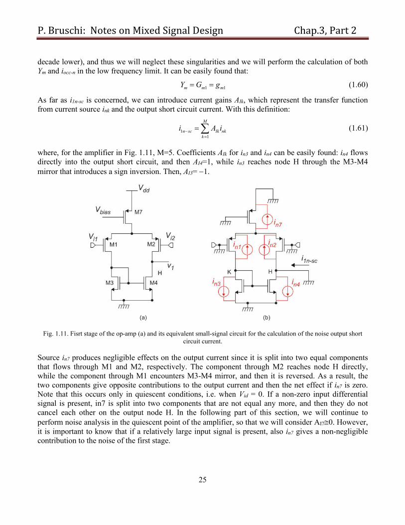
where, for the amplifier in Fig. 1.11, M=5. Coefficients AIk for in3 and in4 can be easily found: in4 flows directly into the output short circuit, and then AI4=1, while in3 reaches node H through the M3-M4 mirror that introduces a sign inversion. Then, AI3= 1.
Fig. 1.11. Fisrt stage of the op-amp (a) and its equivalent small-signal circuit for the calculation of the noise output short circuit current.
Source in7 produces negligible effects on the output current since it is split into two equal components that flows through M1 and M2, respectively. The component through M2 reaches node H directly, while the component through M1 encounters M3-M4 mirror, and then it is reversed. As a result, the two components give opposite contributions to the output current and then the net effect if in7 is zero. Note that this occurs only in quiescent conditions, i.e. when Vid = 0. If a non-zero input differential signal is present, in7 is split into two components that are not equal any more, and then they do not cancel each other on the output node H. In the following part of this section, we will continue to perform noise analysis in the quiescent point of the amplifier, so that we will consider AI70. However, it is important to know that if a relatively large input signal is present, also in7 gives a non-negligible contribution to the noise of the first stage.
P. Bruschi: Notes on Mixed Signal Design Chap.3, Part 2
26
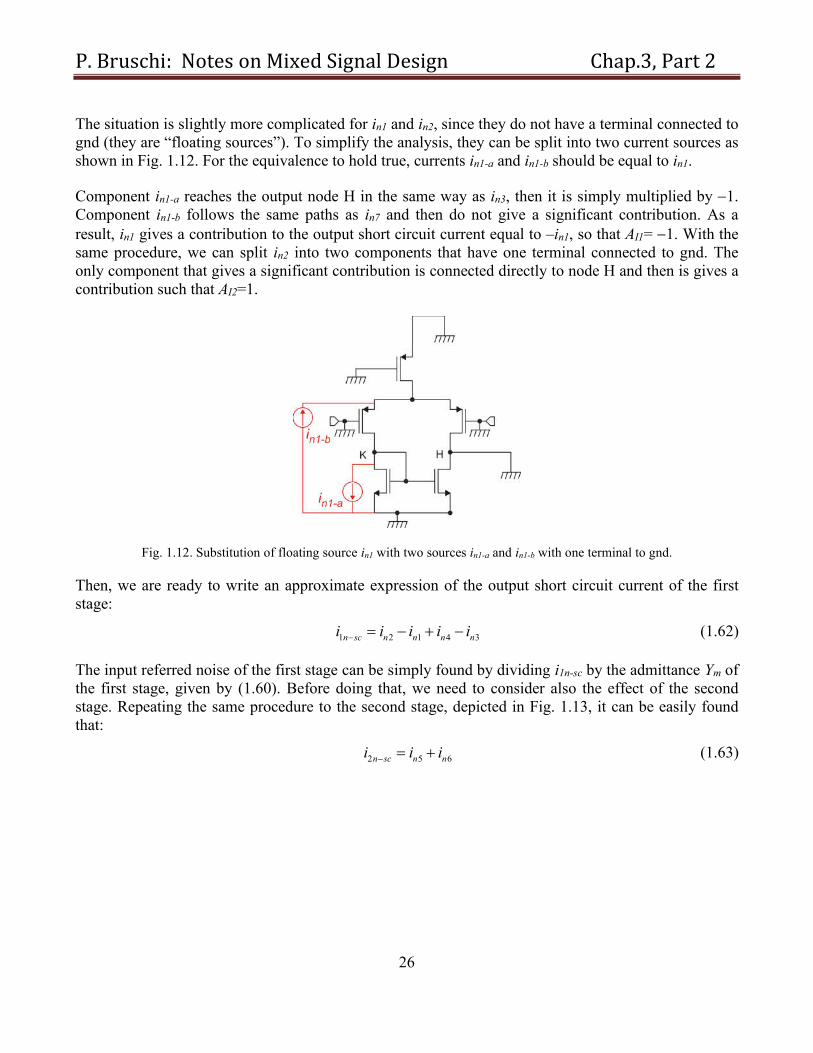
The situation is slightly more complicated for in1 and in2, since they do not have a terminal connected to gnd (they are “floating sources”). To simplify the analysis, they can be split into two current sources as shown in Fig. 1.12. For the equivalence to hold true, currents in1-a and in1-b should be equal to in1.
Component in1-a reaches the output node H in the same way as in3, then it is simply multiplied by 1. Component in1-b follows the same paths as in7 and then do not give a significant contribution. As a result, in1 gives a contribution to the output short circuit current equal to –in1, so that AI1= 1. With the same procedure, we can split in2 into two components that have one terminal connected to gnd. The only component that gives a significant contribution is connected directly to node H and then is gives a contribution such that AI2=1.
Fig. 1.12. Substitution of floating source in1 with two sources in1-a and in1-b with one terminal to gnd.
Then, we are ready to write an approximate expression of the output short circuit current of the first stage:
1 2 1 4 3n sc n n n ni i i i i (1.62)
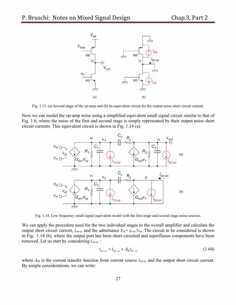
The input referred noise of the first stage can be simply found by dividing i1n-sc by the admittance Ym of the first stage, given by (1.60). Before doing that, we need to consider also the effect of the second stage. Repeating the same procedure to the second stage, depicted in Fig. 1.13, it can be easily found that:
2 5 6n sc n ni i i (1.63)
P. Bruschi: Notes on Mixed Signal Design Chap.3, Part 2
27
Fig. 1.13. (a) Second stage of the op-amp and (b) its equivalent circuit for the output noise short circuit current.
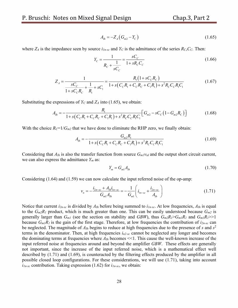
Now we can model the op-amp noise using a simplified equivalent small signal circuit similar to that of Fig. 1.6, where the noise of the first and second stage is simply represented by their output noise short circuit currents. This equivalent circuit is shown in Fig. 1.14 (a).
Fig. 1.14. Low frequency small signal equivalent model with the first stage and second stage noise sources.
We can apply the procedure used for the two individual stages to the overall amplifier and calculate the output short circuit current, ion-sc and the admittance Ym= io-sc/vid. The circuit to be considered is shown in Fig. 1.14 (b), where the output port has been short-circuited and superfluous components have been removed. Let us start by considering ion-sc :
2 1on sc n sc Ih n sci i A i (1.64)
where AIh is the current transfer function from current source i1n-sc and the output short circuit current. By simple considerations, we can write:
P. Bruschi: Notes on Mixed Signal Design Chap.3, Part 2
28
2Ih A m CA Z G Y (1.65)
where ZA is the impedance seen by source i1n-sc and YC is the admittance of the series RC,CC. Then:
1
1 1C
C
C CC
C
sCY
sR CRsC
(1.66)
1
21 1 1 1 1
1
1
11
1 11
C CA
C C C C C C
C C
R sC RZ
sC s C R C R C R s R C R CsCsC R R
(1.67)
Substituting the expressions of YC and ZA into (1.65), we obtain:
12 22
1 1 1 1 1
11
Ih m C m C
C C C C C
RA G sC G R
s C R C R C R s R C R C
(1.68)
With the choice RC=1/Gm2 that we have done to eliminate the RHP zero, we finally obtain:
2 12
1 1 1 1 11m
Ih
C C C C C
G RA
s C R C R C R s R C R C
(1.69)
Considering that AIh is also the transfer function from source Gm1vid and the output short circuit current, we can also express the admittance Ym as:
1m m IhY G A (1.70)
Considering (1.64) and (1.59) we can now calculate the input referred noise of the op-amp:
2 1 21
1 1
1n sc Ih n sc n scn n sc
m Ih m Ih
i A i iv i
G A G A
(1.71)
Notice that current i2n-sc is divided by AIh before being summed to i1n-sc. At low frequencies, AIh is equal to the Gm2R1 product, which is much greater than one. This can be easily understood because Gm2 is generally larger than Gm1 (see the section on stability and GBW), thus Gm2R1>Gm1R1 and Gm1R1>>1 because Gm1R1 is the gain of the first stage. Therefore, at low frequencies the contribution of i2n-sc can be neglected. The magnitude of AIh begins to reduce at high frequencies due to the presence of s and s2 terms in the denominator. Then, at high frequencies in2-sc cannot be neglected any longer and becomes the dominating terms at frequencies where AIh becomes <<1. This cause the well-known increase of the input referred noise at frequencies around and beyond the amplifier GBW. These effects are generally not important, since the increase of the input referred noise, which is a mathematical effect well described by (1.71) and (1.69), is counteracted by the filtering effects produced by the amplifier in all possible closed loop configurations. For these considerations, we will use (1.71), taking into account i1n-sc contribution. Taking expression (1.62) for i1n-sc, we obtain:
P. Bruschi: Notes on Mixed Signal Design Chap.3, Part 2
29
1 2 3 4
1
n n n nn
m
i i i iv
G
(1.72)
The power spectral density (PSD) of the input referred noise, Svn, will be given by:
2
1
312m
iivn
G
SSS
(1.73)
where Si1 and Si3 are the current PSDs of i1 and i3. Due to the symmetry of the circuit we have considered Si2=Si1 and Si4=Si3. All the noise currents have been considered to be independent stochastic processes. A more useful expression can be obtained by transforming the MOSFET current PSDs into the corresponding gate-referred voltage PSDs, according to:
VmI SgS 2 (1.74)
The input referred noise PSD of the amplifier becomes:
2
1
32
312
12m
vmvmvn
G
SgSgS
(1.75)
In the considered amplifier topology, Gm1=gm1, therefore:
32
1
23
12 v
m
mvvn S
g
gSS (1.76)
Indicating with F the ratio gm3/gm1 we can write the following compact formula:
32
12 vvvn SFSS (1.77)
The parameter F can be used to reduce the effect of the mirror MOSFETs on the input referred noise. Writing gm as ID/VTE, we get:
3
13D1
3
1
1
3 sinceTE
TED
TE
TE
D
D
V
VFII
V
V
I
IF (1.78)
In order to reduce the noise contribution of the mirror MOSFETs, we have to make the equivalent thermal voltage VTE of the mirror devices (M3,M4) much larger than that of the input devices. This is usually accomplished by biasing M1 and M2 in weak inversion, or, at least at the lower end of the strong inversion, with |VGSVt|1 nearly equal to 100 mV. The mirror devices should be biased in strong inversion, preferably with (VGSVt)3 of the order of several hundreds mV. This is paid in terms of input common mode range and, considering that (VGSVt)3=(VGSVt)5, also in terms of output swing.
Case 1: Thermal Noise.
Thermal noise can be calculated using (1.76) with the expression Sv=(8/3)kT/gm for Sv1 and Sv3:
P. Bruschi: Notes on Mixed Signal Design Chap.3, Part 2
30
32
1
23
1
1
3
81
3
82
mm
m
m
vng
kTg
g
gkTS (1.79)
Applying elementary simplifications, we obtain:
Fg
kTSm
vn
1
1
3
82
1
(1.80)
The input thermal noise can is then given by the voltage thermal noise of the input devices (M1 and M2) multiplied by a factor (1+F) > 1, which takes into account the additional contribution of the mirror devices M3 and M4. Again, in order to minimize the effect of he latter and be enabled to consider that the noise comes from only the input devices, (VGSVt)3 should be much larger than |VGS-Vt|1, penalizing the input and output ranges.
Now let us express gm1 in (1.80) as ID1/VTE1. After obvious simplifications, we obtain:
FI
VkTS
D
TEvn 1
3
16
1
1 (1.81)
The following considerations can be drawn:
A small thermal noise PSDs is mainly paid in terms of current, i.e power consumption. Remember that the bias current of the first stage, I0, is equal to 2ID1. The higher I0, the smaller Sv1.
Keeping small the input device overdrive voltage, (VGSVt)1, helps reducing the input noise.
Case 2: Flicker Noise.
For M1 and M3 gate referred noise the expression fSv(f)=Nf /(WL) will be used. Equation (1.77) becomes:
33
2
11
2)(LW
NF
LW
NfSf
fnfp
vn (1.82)
where Nfn and Nfp are the flicker noise process parameters for n-MOS and p MOS, respectively. Note that:
a low flicker noise is paid in terms of silicon area
it is possible to save area by reducing the effect of the mirror devices choosing small F factors.
P. Bruschi: Notes on Mixed Signal Design Chap.3, Part 2
31
Design for input offset voltage.
In previous chapter, we have seen that MOSFET parameter variations can be modeled as d.c. current sources placed across the drain and source of the nominal (ideal) device. As in the case of noise, the circuit of Fig.1.11 and the analysis that follows can still be used. Then, expression (1.72) can be used also for the offset voltage:
1 2 3 4
1
p p p p
io
m
i i i iv
G
(1.83)
where currents iip is the currents modeling the process variations of i-th MOSFET. In the following analysis, we will consider that all devices are in strong inversion. Since M1 and M2 as well as M3 and M4 form matched pairs, we can write:
1,21.21 2 1,2 1
1,2 1
3,43.43 4 3,4 3
3,4 3
2
2
tp p D D
GS t
t
p p D D
GS t
Vi i I I
V V
Vi i I I
V V
(1.84)
Substituting the expressions in (1.84) into (1.83) and considering that ID1=ID3, and Gm1=gm1, we get:
3
4,3
1
2,1
4,3
4.3
2,1
2.1
1
122
tGS
t
tGS
t
m
Dio
VV
V
VV
V
g
Iv (1.85)
Finally, in strong inversion ID1/gm1=(VGSVt)1/2, so that the expression of the input offset voltage becomes:
4,32,1
4,3
4.3
2,1
2.11
2tt
tGSio VFV
VVv
(1.86)
where F is given by equation (1.78).
Equation (1.86) can be used to calculate the standard deviation of the offset voltage. Considering that all random variables are independent, we can write:
22222
2
12
4,32,1
4,3
4,3
2,1
2.14 tt VVtGS
vio FVV
(1.87)
The standard deviations can be expressed in terms of the p-MOS and n-MOS matching parameters Cp , CVtp , Cn and CVtn according to:
P. Bruschi: Notes on Mixed Signal Design Chap.3, Part 2
32
33113311
4,32,1
4,3
4,3
2,1
2.1;;;
LW
C
LW
C
LW
C
LW
CVtn
V
Vtp
V
np
tt
(1.88)
Using these expressions equations (1.87) becomes:
3311
2
LW
B
LW
Avio (1.89)
where A and B are given by:
222
2
122
2
1
44Vtnn
tGSVtpp
tGS CFCVV
BCCVV
A
(1.90)
Equation (1.89) indicates that a low offset voltage is paid mainly in terms of area. Once the target vio is given, constants A and B have to be minimized as much as possible in order to save area. As shown by (1.90), the input overdrive voltage (VGS-Vt)1 has to be reduced to the minimum value (around 0.1 V), while F should be made small by making (VGS-Vt)3 several times larger than (VGS-Vt)1.
Once these operations have been performed, M1 and M3 gate areas have to be chosen to obtain the required offset voltage (vio). Clearly, there are infinite solutions to Eqn. (1.89), because we have two unknowns (W1L1, W3L3). If there are no other specifications, it is convenient to find the solution that minimizes the total gate area of M1 and M3, defined as S = W1L1+ W3L3 . If we introduce the following unknown:
11
33
LW
LWa (1.91)
we can rewrite (1.89) as:
a
BA
LWvio
11
2 1 (1.92)
Calculating W1L1 from (1.92) and substituting it into the expression of the area, we find:
aa
BAaLWS
vio
1
11
211 (1.93)
It can be easily shown that the previous expression tends to infinity when a tends either to zero or to infinity. Therefore, a minimum should exist. Calculating the derivative of (1.93) with respect to a and equating it to zero, we find the optimum value of a that minimizes M1 and M3 total area:
A
BaOPT (1.94)
Substituting aOPT into (1.92) we finally find W1L1:
P. Bruschi: Notes on Mixed Signal Design Chap.3, Part 2
33
ABAa
BALW
vioOPTvio
2211
11 (1.95)
Note: the same optimization procedure can be applied to the flicker Noise, since Eqn. (1.82) is formally identical to Eqn. (1.89).
Power consumption.
The power consumption is given by:
SupplyDD IVP (1.96)
where Isupply is the total supply current, equal to:
5110 2 DDsupply IIIII (1.97)
Considering that we can write the drain current ID= gm VTE, the supply current becomes:
55112 TEmTEmsupply VgVgI (1.98)
This equation can be specialized to emphasize the role of either gm1 or gm5. In the case that the dominant specification is the input thermal noise, it is important to show the dependence of gm1, since the thermal noise input spectral density is marked by an inverse proportionality to gm1. Then:
FrVgI
gm
TEm
1211supply (1.99)
where:
5
1
3
1
5
1 ;TE
TE
TE
TE
m
mgm
V
V
V
VF
g
gr (1.100)
In the case that the dominant role is the GBW, it is important to design gm5 in such a way that (1.43) holds. Therefore, we can transform (1.98) to highlight the role of gm5:
P. Bruschi: Notes on Mixed Signal Design Chap.3, Part 2
34
FrVgI gmTEm 2155supply (1.101)
Considering, (1.43) we can directly relate the current consumption to the GBW:
FrGBWCVI gmLTE 212 5supply (1.102)
1.4 References
[1] B. Pellegrini, “Considerations on the feedback theory,” Alta Frequenza, vol. 41, pp. 825-820, Nov. 1972. Available at: http:// brahms.iet.unipi.it/elan/scompos.pdf.
[2] G. Gregorian, G.C. Temes, “Analog MOS Integrated Circuits for Signal Processing”, 1st edition, John Wiley & Sons, New York, 1986, pp.172-176.
[3] G. Palmisano, G. Palumbo, S. Pennisi “Design Procedure for Two-Stage CMOS Transconductance Operational Amplifiers: A Tutorial” Analog Integrated Circuits and Signal Processing, vol. 27, pp. 179-189, 2001.
[4] P. Bruschi, D. Navarrini, G. Tarroboiro, G. Raffa, “A Computationally Efficient Technique for the Optimization of Two Stage CMOS Operational Amplifiers”, proceedings of ECCTD'03 - vol. III, pp. 305-308, Cracovia, September 1-4 2003