Embed Size (px)
Citation preview
1300 Henley Court Pullman, WA 99163
509.334.6306 www.digilentinc.com
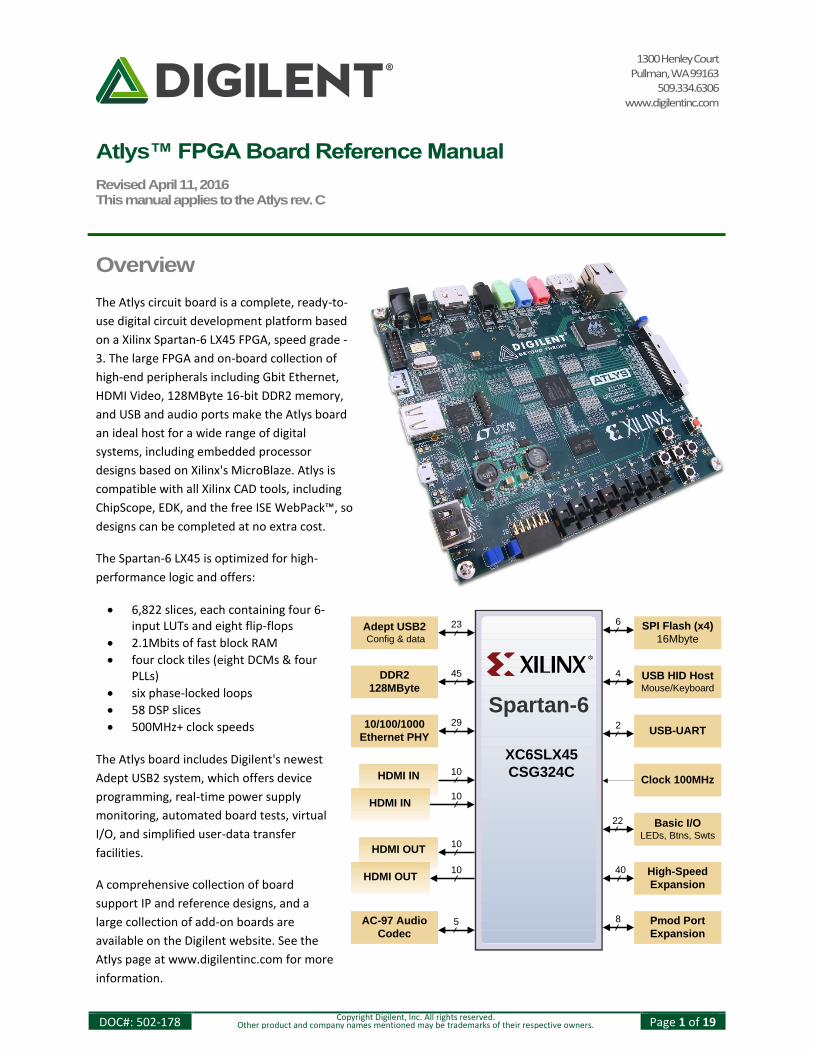
Atlys™ FPGA Board Reference Manual
Revised April 11, 2016 This manual applies to the Atlys rev. C
DOC#: 502-178 Copyright Digilent, Inc. All rights reserved. Other product and company names mentioned may be trademarks of their respective owners. Page 1 of 19
Overview
The Atlys circuit board is a complete, ready-to-
use digital circuit development platform based
on a Xilinx Spartan-6 LX45 FPGA, speed grade -
3. The large FPGA and on-board collection of
high-end peripherals including Gbit Ethernet,
HDMI Video, 128MByte 16-bit DDR2 memory,
and USB and audio ports make the Atlys board
an ideal host for a wide range of digital
systems, including embedded processor
designs based on Xilinx's MicroBlaze. Atlys is
compatible with all Xilinx CAD tools, including
ChipScope, EDK, and the free ISE WebPack™, so
designs can be completed at no extra cost.
The Spartan-6 LX45 is optimized for high-
performance logic and offers:
6,822 slices, each containing four 6-input LUTs and eight flip-flops
2.1Mbits of fast block RAM
four clock tiles (eight DCMs & four PLLs)
six phase-locked loops
58 DSP slices
500MHz+ clock speeds The Atlys board includes Digilent's newest
Adept USB2 system, which offers device
programming, real-time power supply
monitoring, automated board tests, virtual
I/O, and simplified user-data transfer
facilities.
A comprehensive collection of board
support IP and reference designs, and a
large collection of add-on boards are
available on the Digilent website. See the
Atlys page at www.digilentinc.com for more
information.
23
DDR2
128MByte
SPI Flash (x4)
16Mbyte
High-Speed
Expansion
USB HID HostMouse/Keyboard
Spartan-6
XC6SLX45
CSG324C
Basic I/OLEDs, Btns, Swts
Pmod Port
Expansion
45
10
29
22
40
8
4
5
6
USB-UART2
HDMI IN
10HDMI IN
10
HDMI OUT10
HDMI OUT
Clock 100MHz
Adept USB2 Config & data
10/100/1000
Ethernet PHY
AC-97 Audio
Codec
Atlys™ FPGA Board Reference Manual
Copyright Digilent, Inc. All rights reserved. Other product and company names mentioned may be trademarks of their respective owners. Page 2 of 19
Features include:
Xilinx Spartan-6 LX45 FPGA, 324-pin BGA package
128Mbyte DDR2 with 16-bit wide data
10/100/1000 Ethernet PHY
on-board USB2 ports for programming and data transfer
USB-UART and USB-HID port (for mouse/keyboard)
two HDMI video input ports and two HDMI output ports
AC-97 Codec with line-in, line-out, mic, and headphone
real-time power monitors on all power rails
16Mbyte x4 SPI Flash for configuration and data storage
100MHz CMOS oscillator
48 I/O's routed to expansion connectors
GPIO includes eight LEDs, six buttons, and eight slide switches
ships with a 20W power supply and USB cable
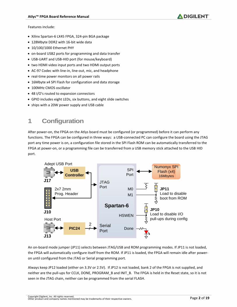
1 Configuration
After power-on, the FPGA on the Atlys board must be configured (or programmed) before it can perform any
functions. The FPGA can be configured in three ways: a USB-connected PC can configure the board using the JTAG
port any time power is on, a configuration file stored in the SPI Flash ROM can be automatically transferred to the
FPGA at power-on, or a programming file can be transferred from a USB memory stick attached to the USB HID
port.
M0
M1
HSWEN
JTAG
Port
USB
Controller
Numonyx SPI
Flash (x4)16Mbytes
2x7 2mm
Prog. Header
SPI
Port
J17
Adept USB Port
Spartan-6
JP11
JP10
Done
J10
Load to disable
boot from ROM
Load to disable I/O
pull-ups during config
PIC24
J13
Host Port
Serial
Port
2
An on-board mode jumper (JP11) selects between JTAG/USB and ROM programming modes. If JP11 is not loaded,
the FPGA will automatically configure itself from the ROM. If JP11 is loaded, the FPGA will remain idle after power-
on until configured from the JTAG or Serial programming port.
Always keep JP12 loaded (either on 3.3V or 2.5V). If JP12 is not loaded, bank 2 of the FPGA is not supplied, and
neither are the pull-ups for CCLK, DONE, PROGRAM_B and INIT_B. The FPGA is held in the Reset state, so it is not
seen in the JTAG chain, neither can be programmed from the serial FLASH.
Atlys™ FPGA Board Reference Manual
Copyright Digilent, Inc. All rights reserved. Other product and company names mentioned may be trademarks of their respective owners. Page 3 of 19
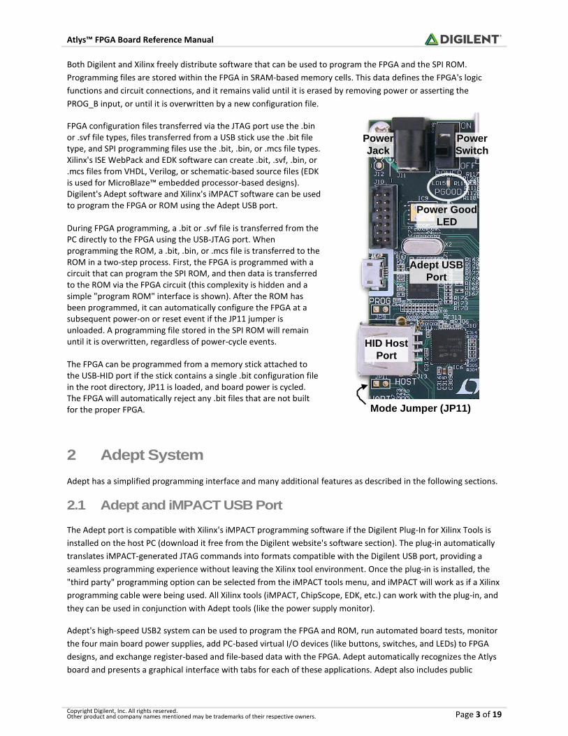
Both Digilent and Xilinx freely distribute software that can be used to program the FPGA and the SPI ROM.
Programming files are stored within the FPGA in SRAM-based memory cells. This data defines the FPGA's logic
functions and circuit connections, and it remains valid until it is erased by removing power or asserting the
PROG_B input, or until it is overwritten by a new configuration file.
FPGA configuration files transferred via the JTAG port use the .bin or .svf file types, files transferred from a USB stick use the .bit file type, and SPI programming files use the .bit, .bin, or .mcs file types. Xilinx's ISE WebPack and EDK software can create .bit, .svf, .bin, or .mcs files from VHDL, Verilog, or schematic-based source files (EDK is used for MicroBlaze™ embedded processor-based designs). Digilent's Adept software and Xilinx's iMPACT software can be used to program the FPGA or ROM using the Adept USB port. During FPGA programming, a .bit or .svf file is transferred from the PC directly to the FPGA using the USB-JTAG port. When programming the ROM, a .bit, .bin, or .mcs file is transferred to the ROM in a two-step process. First, the FPGA is programmed with a circuit that can program the SPI ROM, and then data is transferred to the ROM via the FPGA circuit (this complexity is hidden and a simple "program ROM" interface is shown). After the ROM has been programmed, it can automatically configure the FPGA at a subsequent power-on or reset event if the JP11 jumper is unloaded. A programming file stored in the SPI ROM will remain until it is overwritten, regardless of power-cycle events. The FPGA can be programmed from a memory stick attached to the USB-HID port if the stick contains a single .bit configuration file in the root directory, JP11 is loaded, and board power is cycled. The FPGA will automatically reject any .bit files that are not built for the proper FPGA.
2 Adept System
Adept has a simplified programming interface and many additional features as described in the following sections.
2.1 Adept and iMPACT USB Port
The Adept port is compatible with Xilinx's iMPACT programming software if the Digilent Plug-In for Xilinx Tools is
installed on the host PC (download it free from the Digilent website's software section). The plug-in automatically
translates iMPACT-generated JTAG commands into formats compatible with the Digilent USB port, providing a
seamless programming experience without leaving the Xilinx tool environment. Once the plug-in is installed, the
"third party" programming option can be selected from the iMPACT tools menu, and iMPACT will work as if a Xilinx
programming cable were being used. All Xilinx tools (iMPACT, ChipScope, EDK, etc.) can work with the plug-in, and
they can be used in conjunction with Adept tools (like the power supply monitor).
Adept's high-speed USB2 system can be used to program the FPGA and ROM, run automated board tests, monitor
the four main board power supplies, add PC-based virtual I/O devices (like buttons, switches, and LEDs) to FPGA
designs, and exchange register-based and file-based data with the FPGA. Adept automatically recognizes the Atlys
board and presents a graphical interface with tabs for each of these applications. Adept also includes public
Power Good
LED
Adept USB
Port
Mode Jumper (JP11)
Power
Jack
Power
Switch
HID Host
Port
Atlys™ FPGA Board Reference Manual
Copyright Digilent, Inc. All rights reserved. Other product and company names mentioned may be trademarks of their respective owners. Page 4 of 19
APIs/DLLs so that users can write applications to exchange data with the Atlys board at up to 38Mbytes/sec. The
Adept application, an SDK, and reference materials are freely downloadable from the Digilent website.
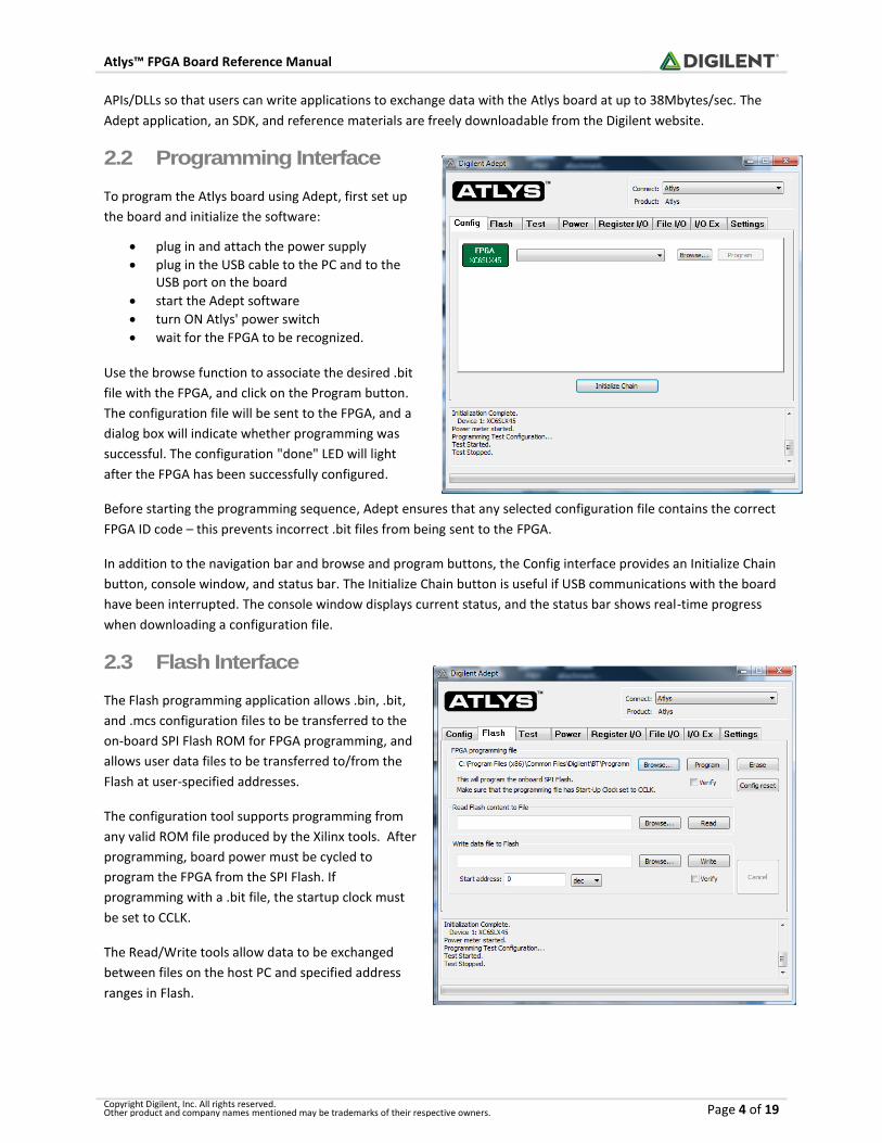
2.2 Programming Interface
To program the Atlys board using Adept, first set up
the board and initialize the software:
plug in and attach the power supply
plug in the USB cable to the PC and to the USB port on the board
start the Adept software
turn ON Atlys' power switch
wait for the FPGA to be recognized. Use the browse function to associate the desired .bit
file with the FPGA, and click on the Program button.
The configuration file will be sent to the FPGA, and a
dialog box will indicate whether programming was
successful. The configuration "done" LED will light
after the FPGA has been successfully configured.
Before starting the programming sequence, Adept ensures that any selected configuration file contains the correct
FPGA ID code – this prevents incorrect .bit files from being sent to the FPGA.
In addition to the navigation bar and browse and program buttons, the Config interface provides an Initialize Chain
button, console window, and status bar. The Initialize Chain button is useful if USB communications with the board
have been interrupted. The console window displays current status, and the status bar shows real-time progress
when downloading a configuration file.
2.3 Flash Interface
The Flash programming application allows .bin, .bit,
and .mcs configuration files to be transferred to the
on-board SPI Flash ROM for FPGA programming, and
allows user data files to be transferred to/from the
Flash at user-specified addresses.
The configuration tool supports programming from
any valid ROM file produced by the Xilinx tools. After
programming, board power must be cycled to
program the FPGA from the SPI Flash. If
programming with a .bit file, the startup clock must
be set to CCLK.
The Read/Write tools allow data to be exchanged
between files on the host PC and specified address
ranges in Flash.
Atlys™ FPGA Board Reference Manual
Copyright Digilent, Inc. All rights reserved. Other product and company names mentioned may be trademarks of their respective owners. Page 5 of 19
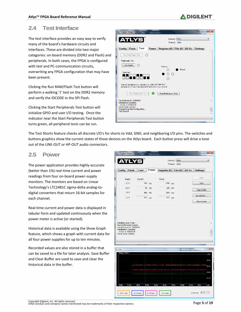
2.4 Test Interface
The test interface provides an easy way to verify
many of the board's hardware circuits and
interfaces. These are divided into two major
categories: on-board memory (DDR2 and Flash) and
peripherals. In both cases, the FPGA is configured
with test and PC-communication circuits,
overwriting any FPGA configuration that may have
been present.
Clicking the Run RAM/Flash Test button will
perform a walking '1' test on the DDR2 memory
and verify the IDCODE in the SPI Flash.
Clicking the Start Peripherals Test button will
initialize GPIO and user I/O testing. Once the
indicator near the Start Peripherals Test button
turns green, all peripheral tests can be run.
The Test Shorts feature checks all discrete I/O's for shorts to Vdd, GND, and neighboring I/O pins. The switches and
buttons graphics show the current states of those devices on the Atlys board. Each button press will drive a tone
out of the LINE-OUT or HP-OUT audio connectors.
2.5 Power
The power application provides highly-accurate
(better than 1%) real-time current and power
readings from four on-board power-supply
monitors. The monitors are based on Linear
Technology's LTC2481C sigma-delta analog-to-
digital converters that return 16-bit samples for
each channel.
Real-time current and power data is displayed in
tabular form and updated continuously when the
power meter is active (or started).
Historical data is available using the Show Graph
feature, which shows a graph with current data for
all four power supplies for up to ten minutes.
Recorded values are also stored in a buffer that
can be saved to a file for later analysis. Save Buffer
and Clear Buffer are used to save and clear the
historical data in the buffer.
Atlys™ FPGA Board Reference Manual
Copyright Digilent, Inc. All rights reserved. Other product and company names mentioned may be trademarks of their respective owners. Page 6 of 19
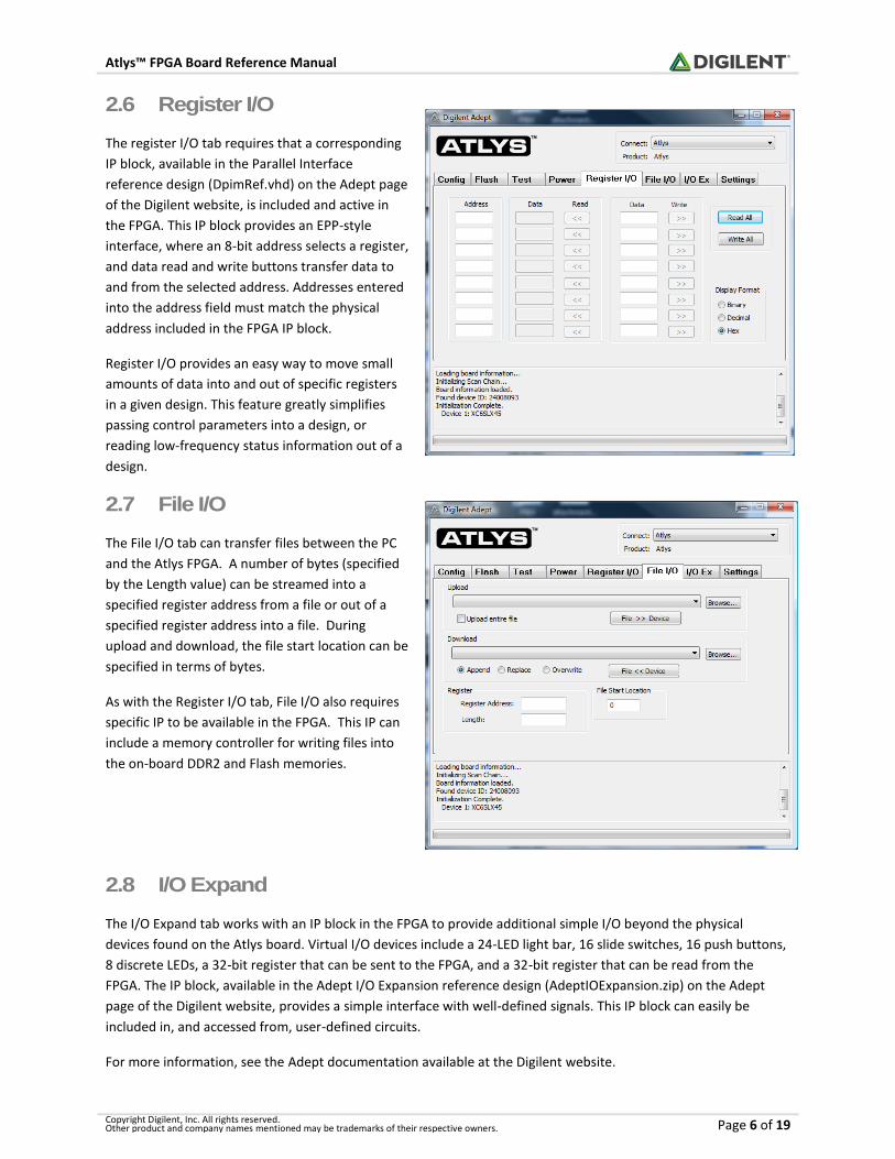
2.6 Register I/O
The register I/O tab requires that a corresponding
IP block, available in the Parallel Interface
reference design (DpimRef.vhd) on the Adept page
of the Digilent website, is included and active in
the FPGA. This IP block provides an EPP-style
interface, where an 8-bit address selects a register,
and data read and write buttons transfer data to
and from the selected address. Addresses entered
into the address field must match the physical
address included in the FPGA IP block.
Register I/O provides an easy way to move small
amounts of data into and out of specific registers
in a given design. This feature greatly simplifies
passing control parameters into a design, or
reading low-frequency status information out of a
design.
2.7 File I/O
The File I/O tab can transfer files between the PC
and the Atlys FPGA. A number of bytes (specified
by the Length value) can be streamed into a
specified register address from a file or out of a
specified register address into a file. During
upload and download, the file start location can be
specified in terms of bytes.
As with the Register I/O tab, File I/O also requires
specific IP to be available in the FPGA. This IP can
include a memory controller for writing files into
the on-board DDR2 and Flash memories.
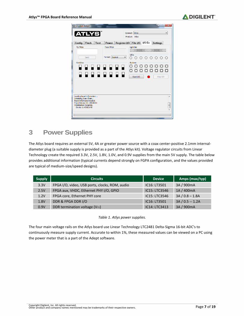
2.8 I/O Expand
The I/O Expand tab works with an IP block in the FPGA to provide additional simple I/O beyond the physical
devices found on the Atlys board. Virtual I/O devices include a 24-LED light bar, 16 slide switches, 16 push buttons,
8 discrete LEDs, a 32-bit register that can be sent to the FPGA, and a 32-bit register that can be read from the
FPGA. The IP block, available in the Adept I/O Expansion reference design (AdeptIOExpansion.zip) on the Adept
page of the Digilent website, provides a simple interface with well-defined signals. This IP block can easily be
included in, and accessed from, user-defined circuits.
For more information, see the Adept documentation available at the Digilent website.
Atlys™ FPGA Board Reference Manual
Copyright Digilent, Inc. All rights reserved. Other product and company names mentioned may be trademarks of their respective owners. Page 7 of 19
3 Power Supplies
The Atlys board requires an external 5V, 4A or greater power source with a coax center-positive 2.1mm internal-
diameter plug (a suitable supply is provided as a part of the Atlys kit). Voltage regulator circuits from Linear
Technology create the required 3.3V, 2.5V, 1.8V, 1.0V, and 0.9V supplies from the main 5V supply. The table below
provides additional information (typical currents depend strongly on FGPA configuration, and the values provided
are typical of medium-size/speed designs).
Table 1. Atlys power supplies.
The four main voltage rails on the Atlys board use Linear Technology LTC2481 Delta-Sigma 16-bit ADC's to
continuously measure supply current. Accurate to within 1%, these measured values can be viewed on a PC using
the power meter that is a part of the Adept software.
Supply Circuits Device Amps (max/typ)
3.3V FPGA I/O, video, USB ports, clocks, ROM, audio IC16: LT3501 3A / 900mA
2.5V FPGA aux, VHDC, Ethernet PHY I/O, GPIO IC15: LTC3546 1A / 400mA
1.2V FPGA core, Ethernet PHY core IC15: LTC3546 3A / 0.8 – 1.8A
1.8V DDR & FPGA DDR I/O IC16: LT3501 3A / 0.5 -- 1.2A
0.9V DDR termination voltage (VTT) IC14: LTC3413 3A / 900mA
Atlys™ FPGA Board Reference Manual
Copyright Digilent, Inc. All rights reserved. Other product and company names mentioned may be trademarks of their respective owners. Page 8 of 19
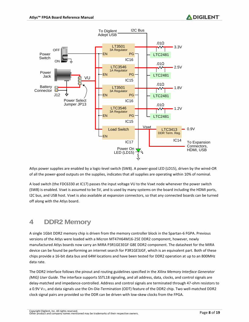
Power Jack
BatteryConnector
Power SelectJumper JP13
VU
1.8V
1.2V
2.5V
3.3V
IC16
IC15
IC16
IC15
ENPowerSwitch
Vswt
IC17
EN
0.9V
.01Ω
LTC2481
To Digilent Adept USB
I2C Bus
IC14To ExpansionConnectors, HDMI, USB
PG
PG
PG
PG
EN
EN
EN
Power OnLED (LD15)
LT35013A Regulator
LTC35461A Regulator
LT35013A Regulator
LTC35463A Regulator
ON
OFF
LTC3413DDR Term. Reg.
Load Switch
J12
.01Ω
LTC2481
.01Ω
LTC2481
.01Ω
LTC2481
Atlys power supplies are enabled by a logic-level switch (SW8). A power-good LED (LD15), driven by the wired-OR
of all the power-good outputs on the supplies, indicates that all supplies are operating within 10% of nominal.
A load switch (the FDC6330 at IC17) passes the input voltage VU to the Vswt node whenever the power switch
(SW8) is enabled. Vswt is assumed to be 5V, and is used by many systems on the board including the HDMI ports,
I2C bus, and USB host. Vswt is also available at expansion connectors, so that any connected boards can be turned
off along with the Atlys board.
4 DDR2 Memory
A single 1Gbit DDR2 memory chip is driven from the memory controller block in the Spartan-6 FGPA. Previous
versions of the Atlys were loaded with a Micron MT47H64M16-25E DDR2 component, however, newly
manufactured Atlys boards now carry an MIRA P3R1GE3EGF G8E DDR2 component. The datasheet for the MIRA
device can be found be performing an internet search for P3R1GE3JGF, which is an equivalent part. Both of these
chips provide a 16-bit data bus and 64M locations and have been tested for DDR2 operation at up to an 800MHz
data rate.
The DDR2 interface follows the pinout and routing guidelines specified in the Xilinx Memory Interface Generator
(MIG) User Guide. The interface supports SSTL18 signaling, and all address, data, clocks, and control signals are
delay-matched and impedance-controlled. Address and control signals are terminated through 47-ohm resistors to
a 0.9V VTT, and data signals use the On-Die-Termination (ODT) feature of the DDR2 chip. Two well-matched DDR2
clock signal pairs are provided so the DDR can be driven with low-skew clocks from the FPGA.
Atlys™ FPGA Board Reference Manual
Copyright Digilent, Inc. All rights reserved. Other product and company names mentioned may be trademarks of their respective owners. Page 9 of 19
When generating a MIG core for the MIRA part, selecting the "EDE1116AXXX-8E" device will result in the correct
timing parameters being set. When generating a component for the Micron part, it can be selected by name within
the wizard. The part loaded on your Atlys can be determined by examining the print on the DDR2 component
(IC13).
DQ[15:0]
13
16
AD[12:0]
RAS#
CAS#
WE#
BA0
BA1
BA2
See Table
CS#
L4
P1
P2
E1
F1
F2
E3
K5
L5
Spartan-6
DDR2
x14
VREF
CKE
CK
CK#
UDQS_P
UDQS_N
LDQS_P
LDQS_N
UDM
LDM
ODT
1V8
L3
K4
K3
K6
H7
G1
G3
5 Flash Memory
The Atlys board uses a128Mbit Numonyx N25Q12 Serial Flash memory
device (organized as 16-bit by 16Mbytes) for non-volatile storage of
FPGA configuration files. The SPI Flash can be programmed with a .bit,
.bin., or .mcs file using the Adept software. An FPGA configuration file
requires less than 12Mbits, leaving 116Mbits available for user data.
Data can be transferred from a PC to/from the Flash by user
applications, or by facilities built into the Adept software. User designs
programmed into the FPGA can also transfer data to and from the
ROM. A reference design on the Digilent website provides an example
of driving the Flash memory from an FPGA-based design.
A board test/demonstration program is loaded into the SPI Flash during manufacturing. That configuration, also
available on the Digilent webpage, can be used to demonstrate and check all of the devices and circuits on the
Atlys board.
Address
A12: G6 A4: F3
A11: D3 A3: L7
A10: F4 A2: H5
A9: D1 A1: J6
A8: D2 A0: J7
A7: H6
A6: H3
A5: H4
Data
D15: U1 D7: J1
D14: U2 D6: J3
D13: T1 D5: H1
D12: T2 D4: H2
D11: N1 D3: K1
D10: N2 D2: K2
D9: M1 D1: L1
D8: M3 D0: L2
CS#
SDI/DQ0
SDO/DQ1
AH18
AF20
AF14
AE14
Spartan-6 SPI Flash
WP#/DQ2
HLD#/DQ3
AG21
AG17
SCK
Atlys™ FPGA Board Reference Manual
Copyright Digilent, Inc. All rights reserved. Other product and company names mentioned may be trademarks of their respective owners. Page 10 of 19
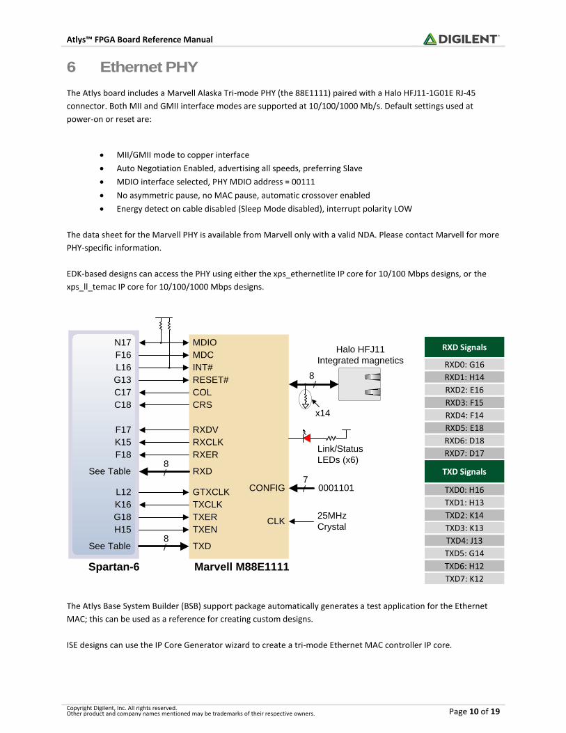
6 Ethernet PHY
The Atlys board includes a Marvell Alaska Tri-mode PHY (the 88E1111) paired with a Halo HFJ11-1G01E RJ-45
connector. Both MII and GMII interface modes are supported at 10/100/1000 Mb/s. Default settings used at
power-on or reset are:
MII/GMII mode to copper interface
Auto Negotiation Enabled, advertising all speeds, preferring Slave
MDIO interface selected, PHY MDIO address = 00111
No asymmetric pause, no MAC pause, automatic crossover enabled
Energy detect on cable disabled (Sleep Mode disabled), interrupt polarity LOW
The data sheet for the Marvell PHY is available from Marvell only with a valid NDA. Please contact Marvell for more
PHY-specific information.
EDK-based designs can access the PHY using either the xps_ethernetlite IP core for 10/100 Mbps designs, or the
xps_ll_temac IP core for 10/100/1000 Mbps designs.
See Table
K15
F17
L16
F16
N17
Spartan-6
G13
C17
INT#
RESET#
COL
CRS
RXDV
RXCLK
RXER
GTXCLK
TXCLK
TXER
TXEN
MDIO
8
25MHz
Crystal
MDC
CONFIG7
0001101
CLK
See Table
C18
L12
K16
G18
H15
RXD
TXD
8
8
Marvell M88E1111
x14
Halo HFJ11
Integrated magnetics
F18Link/Status
LEDs (x6)
The Atlys Base System Builder (BSB) support package automatically generates a test application for the Ethernet
MAC; this can be used as a reference for creating custom designs.
ISE designs can use the IP Core Generator wizard to create a tri-mode Ethernet MAC controller IP core.
RXD Signals
RXD0: G16
RXD1: H14
RXD2: E16
RXD3: F15
RXD4: F14
RXD5: E18
RXD6: D18
RXD7: D17
TXD Signals
TXD0: H16
TXD1: H13
TXD2: K14
TXD3: K13
TXD4: J13
TXD5: G14
TXD6: H12
TXD7: K12
Atlys™ FPGA Board Reference Manual
Copyright Digilent, Inc. All rights reserved. Other product and company names mentioned may be trademarks of their respective owners. Page 11 of 19
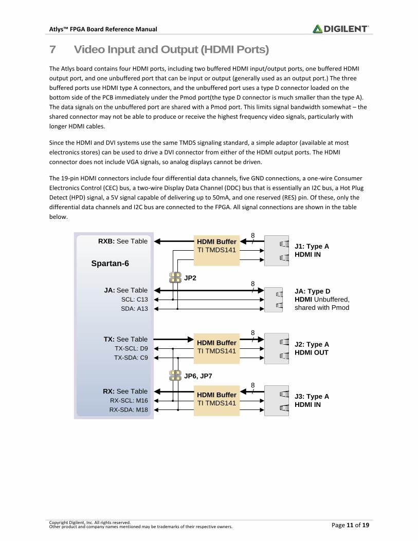
7 Video Input and Output (HDMI Ports)
The Atlys board contains four HDMI ports, including two buffered HDMI input/output ports, one buffered HDMI
output port, and one unbuffered port that can be input or output (generally used as an output port.) The three
buffered ports use HDMI type A connectors, and the unbuffered port uses a type D connector loaded on the
bottom side of the PCB immediately under the Pmod port(the type D connector is much smaller than the type A).
The data signals on the unbuffered port are shared with a Pmod port. This limits signal bandwidth somewhat – the
shared connector may not be able to produce or receive the highest frequency video signals, particularly with
longer HDMI cables.
Since the HDMI and DVI systems use the same TMDS signaling standard, a simple adaptor (available at most
electronics stores) can be used to drive a DVI connector from either of the HDMI output ports. The HDMI
connector does not include VGA signals, so analog displays cannot be driven.
The 19-pin HDMI connectors include four differential data channels, five GND connections, a one-wire Consumer
Electronics Control (CEC) bus, a two-wire Display Data Channel (DDC) bus that is essentially an I2C bus, a Hot Plug
Detect (HPD) signal, a 5V signal capable of delivering up to 50mA, and one reserved (RES) pin. Of these, only the
differential data channels and I2C bus are connected to the FPGA. All signal connections are shown in the table
below.
See Table
Spartan-6
8
8
HDMI Buffer
TI TMDS141J1: Type A
HDMI IN
8
J3: Type A
HDMI IN
8
HDMI Buffer
TI TMDS141
J2: Type A
HDMI OUT
JA: Type D
HDMI Unbuffered,
shared with Pmod
HDMI Buffer
TI TMDS141
See Table
See Table
See Table
SCL: C13
SDA: A13
TX-SDA: C9
TX-SCL: D9
RX-SDA: M18
RX-SCL: M16
JP6, JP7
JP2
RXB:
JA:
TX:
RX:
Atlys™ FPGA Board Reference Manual
Copyright Digilent, Inc. All rights reserved. Other product and company names mentioned may be trademarks of their respective owners. Page 12 of 19
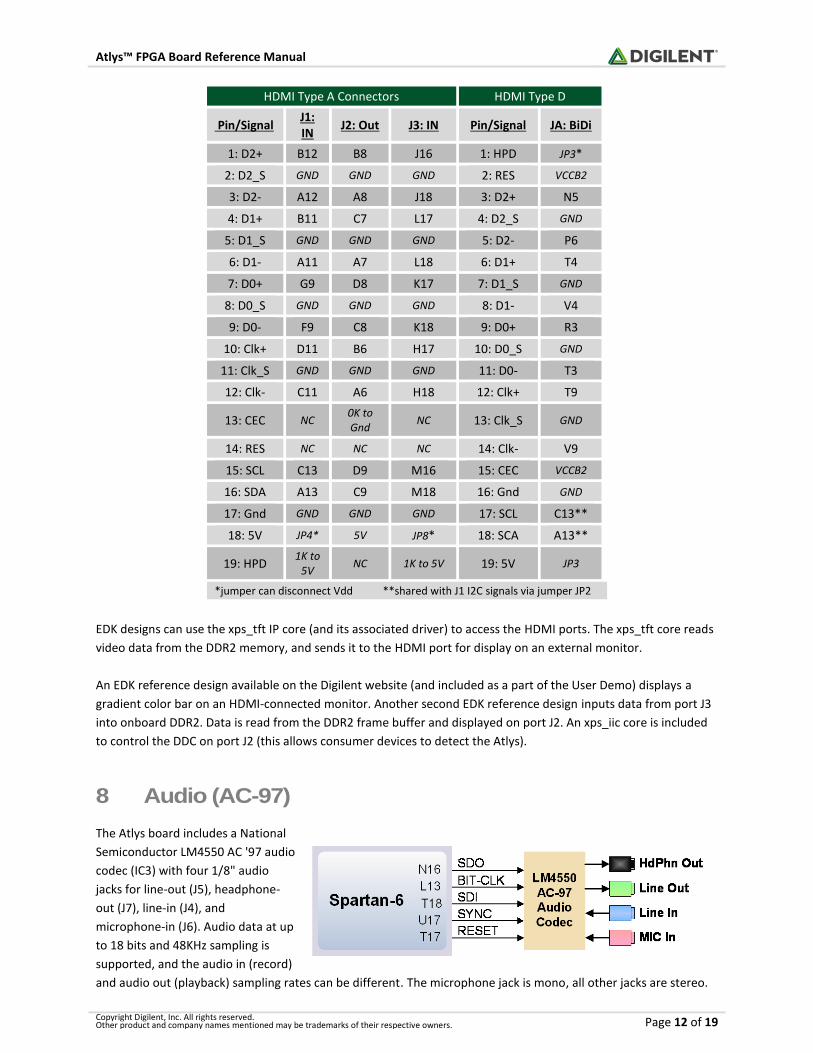
HDMI Type A Connectors HDMI Type D
Pin/Signal J1: IN
J2: Out J3: IN Pin/Signal JA: BiDi
1: D2+ B12 B8 J16 1: HPD JP3*
2: D2_S GND GND GND 2: RES VCCB2
3: D2- A12 A8 J18 3: D2+ N5
4: D1+ B11 C7 L17 4: D2_S GND
5: D1_S GND GND GND 5: D2- P6
6: D1- A11 A7 L18 6: D1+ T4
7: D0+ G9 D8 K17 7: D1_S GND
8: D0_S GND GND GND 8: D1- V4
9: D0- F9 C8 K18 9: D0+ R3
10: Clk+ D11 B6 H17 10: D0_S GND
11: Clk_S GND GND GND 11: D0- T3
12: Clk- C11 A6 H18 12: Clk+ T9
13: CEC NC 0K to Gnd
NC 13: Clk_S GND
14: RES NC NC NC 14: Clk- V9
15: SCL C13 D9 M16 15: CEC VCCB2
16: SDA A13 C9 M18 16: Gnd GND
17: Gnd GND GND GND 17: SCL C13**
18: 5V JP4* 5V JP8* 18: SCA A13**
19: HPD 1K to
5V NC 1K to 5V 19: 5V JP3
*jumper can disconnect Vdd **shared with J1 I2C signals via jumper JP2
EDK designs can use the xps_tft IP core (and its associated driver) to access the HDMI ports. The xps_tft core reads
video data from the DDR2 memory, and sends it to the HDMI port for display on an external monitor.
An EDK reference design available on the Digilent website (and included as a part of the User Demo) displays a
gradient color bar on an HDMI-connected monitor. Another second EDK reference design inputs data from port J3
into onboard DDR2. Data is read from the DDR2 frame buffer and displayed on port J2. An xps_iic core is included
to control the DDC on port J2 (this allows consumer devices to detect the Atlys).
8 Audio (AC-97)
The Atlys board includes a National
Semiconductor LM4550 AC '97 audio
codec (IC3) with four 1/8" audio
jacks for line-out (J5), headphone-
out (J7), line-in (J4), and
microphone-in (J6). Audio data at up
to 18 bits and 48KHz sampling is
supported, and the audio in (record)
and audio out (playback) sampling rates can be different. The microphone jack is mono, all other jacks are stereo.
Atlys™ FPGA Board Reference Manual
Copyright Digilent, Inc. All rights reserved. Other product and company names mentioned may be trademarks of their respective owners. Page 13 of 19
The headphone jack is driven by the audio codec's internal 50mW amplifier. The table below summarizes the audio
signals.
The LM4550 audio codec is compliant to the AC '97 v2.1 (Intel) standard and is connected as a Primary Codec (ID1
= 0, ID0 = 0). The table below shows the AC '97 codec control and data signals. All signals are LVCMOS33.
Signal Name FPGA Pin Pin Function
AUD-BIT-CLK L13 12.288MHZ serial clock output, driven at one-half the frequency of the 24.576MHz crystal input (XTL_IN).
AUD-SDI T18 Serial Data In (to the FPGA) from the codec. SDI data consists of AC '97 Link Input frames that contain both configuration and PCM audio data. SDI data is driven on the rising edge of AUD-BIT-CLK.
AUD-SDO N16 Serial Data Out (to the codec) from the FPGA. SDO data consists of AC '97 Link Output frames that contain both configuration and DAC audio data. SDO is sampled by the LM4550 on the falling edge of AUD-BIT-CLK.
AUD-SYNC U17
AC Link frame marker and Warm Reset. SYNC (input to the codec) defines AC Link frame boundaries. Each frame lasts 256 periods of AUD-BIT-CLK. SYNC is normally a 48kHz positive pulse with a duty cycle of 6.25% (16/256). SYNC is sampled on the rising edge of AUD-BIT-CLK, and the codec takes the first positive sample of SYNC as defining the start of a new AC Link frame. If a subsequent SYNC pulse occurs within 255 AUD-BIT-CLK periods of the frame start it will be ignored. SYNC is also used as an active high input to perform an (asynchronous) Warm Reset. Warm Reset is used to clear a power- down state on the codec AC Link interface.
AUD-RESET T17
Cold Reset. This active low signal causes a hardware reset which returns the control registers and all internal circuits to their default conditions. RESET must be used to initialize the LM4550 after Power On when the supplies have stabilized. RESET also clears the codec from both ATE and Vendor test modes. In addition, while active, it switches the PC_BEEP mono input directly to both channels of the LINE_OUT stereo output.
The EDK reference design (available on the Digilent website) leverages our custom AC-97 pcore to accomplish
several standard audio processing tasks such as recording and playing back audio data.
9 Oscillators/Clocks
The Atlys board includes a single 100MHz CMOS oscillator connected to pin L15 (L15 is a GCLK input in bank 1). The
input clock can drive any or all of the four clock management tiles in the Spartan-6. Each tile includes two Digital
Clock Managers (DCMs) and four Phase-Locked Loops (PLLs).
DCMs provide the four phases of the input frequency (0º, 90º, 180º, and 270º), a divided clock that can be the
input clock divided by any integer from 2 to 16 or 1.5, 2.5, 3.5... 7.5, and two antiphase clock outputs that can be
multiplied by any integer from 2 to 32 and simultaneously divided by any integer from 1 to 32.
PLLs use VCOs that can be programmed to generate frequencies in the 400MHz to 1080MHz range by setting three
sets of programmable dividers during FPAG configuration. VCO outputs have eight equally-spaced outputs (0º, 45º,
90º, 135º, 180º, 225º, 270º, and 315º) that can be divided by any integer between 1 and 128.
Atlys™ FPGA Board Reference Manual
Copyright Digilent, Inc. All rights reserved. Other product and company names mentioned may be trademarks of their respective owners. Page 14 of 19
Spartan-6
P17
PIC24FJ192
K_CLK
N15
“HOST”J13
2 N18
P18
K_DAT
M_CLK
M_DAT
R13
R15
DIN
CLK
FPGA Serial
programming
PS/2 Keyboard
PS/2 Mouse
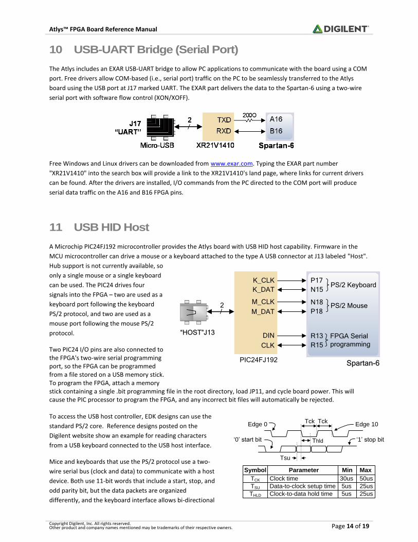
10 USB-UART Bridge (Serial Port)
The Atlys includes an EXAR USB-UART bridge to allow PC applications to communicate with the board using a COM
port. Free drivers allow COM-based (i.e., serial port) traffic on the PC to be seamlessly transferred to the Atlys
board using the USB port at J17 marked UART. The EXAR part delivers the data to the Spartan-6 using a two-wire
serial port with software flow control (XON/XOFF).
Free Windows and Linux drivers can be downloaded from www.exar.com. Typing the EXAR part number
"XR21V1410" into the search box will provide a link to the XR21V1410's land page, where links for current drivers
can be found. After the drivers are installed, I/O commands from the PC directed to the COM port will produce
serial data traffic on the A16 and B16 FPGA pins.
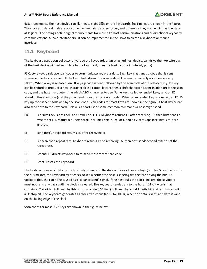
11 USB HID Host
A Microchip PIC24FJ192 microcontroller provides the Atlys board with USB HID host capability. Firmware in the
MCU microcontroller can drive a mouse or a keyboard attached to the type A USB connector at J13 labeled "Host".
Hub support is not currently available, so
only a single mouse or a single keyboard
can be used. The PIC24 drives four
signals into the FPGA – two are used as a
keyboard port following the keyboard
PS/2 protocol, and two are used as a
mouse port following the mouse PS/2
protocol.
Two PIC24 I/O pins are also connected to the FPGA's two-wire serial programming port, so the FPGA can be programmed from a file stored on a USB memory stick. To program the FPGA, attach a memory stick containing a single .bit programming file in the root directory, load JP11, and cycle board power. This will cause the PIC processor to program the FPGA, and any incorrect bit files will automatically be rejected. To access the USB host controller, EDK designs can use the
standard PS/2 core. Reference designs posted on the
Digilent website show an example for reading characters
from a USB keyboard connected to the USB host interface.
Mice and keyboards that use the PS/2 protocol use a two-
wire serial bus (clock and data) to communicate with a host
device. Both use 11-bit words that include a start, stop, and
odd parity bit, but the data packets are organized
differently, and the keyboard interface allows bi-directional
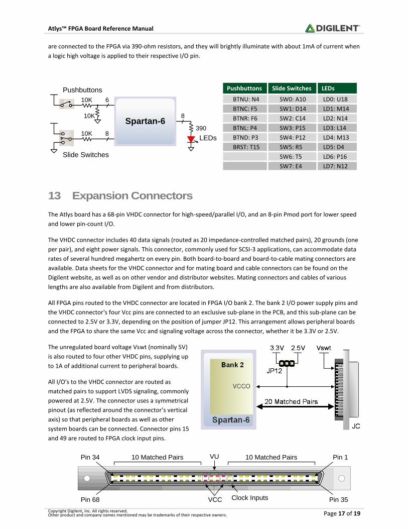
TCK
TSU
Clock time
Data-to-clock setup time
30us
5us
50us
25us
Symbol Parameter Min Max
THLD Clock-to-data hold time 5us 25us
Edge 0
‘0’ start bit ‘1’ stop bit
Edge 10
Tsu
Thld
Tck Tck
Atlys™ FPGA Board Reference Manual
Copyright Digilent, Inc. All rights reserved. Other product and company names mentioned may be trademarks of their respective owners. Page 15 of 19
data transfers (so the host device can illuminate state LEDs on the keyboard). Bus timings are shown in the figure.
The clock and data signals are only driven when data transfers occur, and otherwise they are held in the idle state
at logic '1'. The timings define signal requirements for mouse-to-host communications and bi-directional keyboard
communications. A PS/2 interface circuit can be implemented in the FPGA to create a keyboard or mouse
interface.
11.1 Keyboard
The keyboard uses open-collector drivers so the keyboard, or an attached host device, can drive the two-wire bus
(if the host device will not send data to the keyboard, then the host can use input-only ports).
PS/2-style keyboards use scan codes to communicate key press data. Each key is assigned a code that is sent
whenever the key is pressed. If the key is held down, the scan code will be sent repeatedly about once every
100ms. When a key is released, an F0 key-up code is sent, followed by the scan code of the released key. If a key
can be shifted to produce a new character (like a capital letter), then a shift character is sent in addition to the scan
code, and the host must determine which ASCII character to use. Some keys, called extended keys, send an E0
ahead of the scan code (and they may send more than one scan code). When an extended key is released, an E0 F0
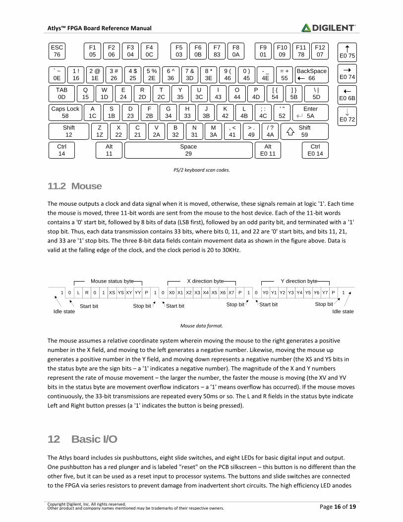
key-up code is sent, followed by the scan code. Scan codes for most keys are shown in the figure. A host device can
also send data to the keyboard. Below is a short list of some common commands a host might send.
ED Set Num Lock, Caps Lock, and Scroll Lock LEDs. Keyboard returns FA after receiving ED, then host sends a
byte to set LED status: bit 0 sets Scroll Lock, bit 1 sets Num Lock, and bit 2 sets Caps lock. Bits 3 to 7 are
ignored.
EE Echo (test). Keyboard returns EE after receiving EE.
F3 Set scan code repeat rate. Keyboard returns F3 on receiving FA, then host sends second byte to set the
repeat rate.
FE Resend. FE directs keyboard to re-send most recent scan code.
FF Reset. Resets the keyboard.
The keyboard can send data to the host only when both the data and clock lines are high (or idle). Since the host is
the bus master, the keyboard must check to see whether the host is sending data before driving the bus. To
facilitate this, the clock line is used as a "clear to send" signal. If the host pulls the clock line low, the keyboard
must not send any data until the clock is released. The keyboard sends data to the host in 11-bit words that
contain a '0' start bit, followed by 8-bits of scan code (LSB first), followed by an odd parity bit and terminated with
a '1' stop bit. The keyboard generates 11 clock transitions (at 20 to 30KHz) when the data is sent, and data is valid
on the falling edge of the clock.
Scan codes for most PS/2 keys are shown in the figure below.
Atlys™ FPGA Board Reference Manual
Copyright Digilent, Inc. All rights reserved. Other product and company names mentioned may be trademarks of their respective owners. Page 16 of 19
ESC
76
` ~
0E
TAB
0D
Caps Lock
58
Shift
12
Ctrl
14
1 !
16
2 @
1E
3 #
26
4 $
25
5 %
2E
Q
15
W
1D
E
24
R
2D
T
2C
A
1C
S
1B
D
23
F
2B
G
34
Z
1Z
X
22
C
21
V
2A
B
32
6 ^
36
7 &
3D
8 *
3E
9 (
46
0 )
45
- _
4E
= +
55
BackSpace
66
Y
35
U
3C
I
43
O
44
P
4D
[ {
54
] }
5B
\ |
5D
H
33
J
3B
K
42
L
4B
; :
4C
' "
52
Enter
5A
N
31
M
3A
, <
41
> .
49
/ ?
4A
Shift
59
Alt
11
Space
29
Alt
E0 11
Ctrl
E0 14
F1
05
F2
06
F3
04
F4
0C
F5
03
F6
0B
F7
83
F8
0A
F9
01
F10
09
F11
78
F12
07 E0 75
E0 74
E0 6B
E0 72
PS/2 keyboard scan codes.
11.2 Mouse
The mouse outputs a clock and data signal when it is moved, otherwise, these signals remain at logic '1'. Each time
the mouse is moved, three 11-bit words are sent from the mouse to the host device. Each of the 11-bit words
contains a '0' start bit, followed by 8 bits of data (LSB first), followed by an odd parity bit, and terminated with a '1'
stop bit. Thus, each data transmission contains 33 bits, where bits 0, 11, and 22 are '0' start bits, and bits 11, 21,
and 33 are '1' stop bits. The three 8-bit data fields contain movement data as shown in the figure above. Data is
valid at the falling edge of the clock, and the clock period is 20 to 30KHz.
L R 0 1 XS YS XY YY P X0 X1 X2 X3 X4 X5 X6 X7 P Y0 Y1 Y2 Y3 Y4 Y5 Y6 Y7 P1 0 1 00 11
Idle stateStart bit
Mouse status byte X direction byte Y direction byte
Stop bit Start bit Stop bit
Idle stateStop bit Start bit
Mouse data format.
The mouse assumes a relative coordinate system wherein moving the mouse to the right generates a positive
number in the X field, and moving to the left generates a negative number. Likewise, moving the mouse up
generates a positive number in the Y field, and moving down represents a negative number (the XS and YS bits in
the status byte are the sign bits – a '1' indicates a negative number). The magnitude of the X and Y numbers
represent the rate of mouse movement – the larger the number, the faster the mouse is moving (the XV and YV
bits in the status byte are movement overflow indicators – a '1' means overflow has occurred). If the mouse moves
continuously, the 33-bit transmissions are repeated every 50ms or so. The L and R fields in the status byte indicate
Left and Right button presses (a '1' indicates the button is being pressed).
12 Basic I/O
The Atlys board includes six pushbuttons, eight slide switches, and eight LEDs for basic digital input and output.
One pushbutton has a red plunger and is labeled "reset" on the PCB silkscreen – this button is no different than the
other five, but it can be used as a reset input to processor systems. The buttons and slide switches are connected
to the FPGA via series resistors to prevent damage from inadvertent short circuits. The high efficiency LED anodes
Atlys™ FPGA Board Reference Manual
Copyright Digilent, Inc. All rights reserved. Other product and company names mentioned may be trademarks of their respective owners. Page 17 of 19
Spartan-6
Slide Switches
10K
10K
10KLEDs
390
8
6
8
Pushbuttons
are connected to the FPGA via 390-ohm resistors, and they will brightly illuminate with about 1mA of current when
a logic high voltage is applied to their respective I/O pin.
13 Expansion Connectors
The Atlys board has a 68-pin VHDC connector for high-speed/parallel I/O, and an 8-pin Pmod port for lower speed
and lower pin-count I/O.
The VHDC connector includes 40 data signals (routed as 20 impedance-controlled matched pairs), 20 grounds (one
per pair), and eight power signals. This connector, commonly used for SCSI-3 applications, can accommodate data
rates of several hundred megahertz on every pin. Both board-to-board and board-to-cable mating connectors are
available. Data sheets for the VHDC connector and for mating board and cable connectors can be found on the
Digilent website, as well as on other vendor and distributor websites. Mating connectors and cables of various
lengths are also available from Digilent and from distributors.
All FPGA pins routed to the VHDC connector are located in FPGA I/O bank 2. The bank 2 I/O power supply pins and
the VHDC connector's four Vcc pins are connected to an exclusive sub-plane in the PCB, and this sub-plane can be
connected to 2.5V or 3.3V, depending on the position of jumper JP12. This arrangement allows peripheral boards
and the FPGA to share the same Vcc and signaling voltage across the connector, whether it be 3.3V or 2.5V.
The unregulated board voltage Vswt (nominally 5V)
is also routed to four other VHDC pins, supplying up
to 1A of additional current to peripheral boards.
All I/O's to the VHDC connector are routed as
matched pairs to support LVDS signaling, commonly
powered at 2.5V. The connector uses a symmetrical
pinout (as reflected around the connector's vertical
axis) so that peripheral boards as well as other
system boards can be connected. Connector pins 15
and 49 are routed to FPGA clock input pins.
Pushbuttons Slide Switches LEDs
BTNU: N4 SW0: A10 LD0: U18
BTNC: F5 SW1: D14 LD1: M14
BTNR: F6 SW2: C14 LD2: N14
BTNL: P4 SW3: P15 LD3: L14
BTND: P3 SW4: P12 LD4: M13
BRST: T15 SW5: R5 LD5: D4
SW6: T5 LD6: P16
SW7: E4 LD7: N12
VUPin 34
Pin 68
Pin 1
Pin 35VCC
10 Matched Pairs 10 Matched Pairs
Clock Inputs
Atlys™ FPGA Board Reference Manual
Copyright Digilent, Inc. All rights reserved. Other product and company names mentioned may be trademarks of their respective owners. Page 18 of 19
VHDC Connector Pinout
IO1-P: U16 IO1-N: V16 IO11-P: U10 IO11-N: V10
IO2-P: U15 IO2-N: V15 IO12-P: R8 IO12-N: T8
IO3-P: U13 IO3-N: V13 IO13-P: M8 IO13-N: N8
IO4-P: M11 IO4-N: N11 IO14-P: U8 IO14-N: V8
IO5-P: R11 IO5-N: T11 IO15-P: U7 IO15-N: V7
IO6-P: T12 IO6-N: V12 IO16-P: N7 IO16-N: P8
IO7-P: N10 IO7-N: P11 IO17-P: T6 IO17-N: V6
IO8-P: M10 IO8-N: N9 IO18-P: R7 IO18-N: T7
IO9-P: U11 IO9-N: V11 IO19-P: N6 IO19-N: P7
IO10-P: R10 IO10-N: T10 IO20-P: U5 IO20-N: V5
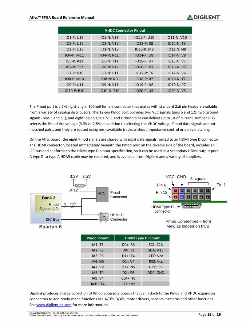
The Pmod port is a 2x6 right-angle, 100-mil female connector that mates with standard 2x6 pin headers available
from a variety of catalog distributors. The 12-pin Pmod port provides two VCC signals (pins 6 and 12), two Ground
signals (pins 5 and 11), and eight logic signals. VCC and Ground pins can deliver up to 1A of current. Jumper JP12
selects the Pmod Vcc voltage (3.3V or 2.5V) in addition to selecting the VHDC voltage. Pmod data signals are not
matched pairs, and they are routed using best-available tracks without impedance control or delay matching.
On the Atlys board, the eight Pmod signals are shared with eight data signals routed to an HDMI type D connector.
The HDMI connector, located immediately beneath the Pmod port on the reverse side of the board, includes an
I2C bus and conforms to the HDMI type D pinout specification, so it can be used as a secondary HDMI output port.
A type D to type A HDMI cable may be required, and is available from Digilent and a variety of suppliers.
Pmod
Signals (x8)
Bank 2
Pin 1
Pin 12
Pin 6
8 signalsVCC GND
VCC Pmod
Connector
Pmod Connectors – front
view as loaded on PCB
50Ω
3.3V 2.5V
JP12
HDMI Type D
connectorHDMI-D
Connector
8
I2C Bus
Spartan-6
Digilent produces a large collection of Pmod accessory boards that can attach to the Pmod and VHDC expansion
connectors to add ready-made functions like A/D's, D/A's, motor drivers, sensors, cameras and other functions.
See www.digilentinc.com for more information.
Pmod Pinout HDMI Type D Pinout
JA1: T3 D0+: R3 SCL: C13
JA2: R3 D0-: T3 SDA: A13
JA3: P6 D1+: T4 CEC: Vcc
JA4: N5 D1-: V4 RES: Vcc
JA7: V9 D2+: N5 HPD: 5V
JA8: T9 D2-: P6 DDC: GND
JA9: V4 CLK+: T9
JA10: T4 CLK-: V9
Atlys™ FPGA Board Reference Manual
Copyright Digilent, Inc. All rights reserved. Other product and company names mentioned may be trademarks of their respective owners. Page 19 of 19
14 Built-In Self Test
A demonstration configuration is loaded into the SPI Flash ROM on the Atlys board during manufacturing. This
demo, also available on the Digilent website, can serve as a board verification test since it interacts with all devices
and ports on the board. When Atlys powers up, if the demonstration image is present in the SPI Flash, the DDR is
tested, and then a bitmap image file will be transferred from the SPI Flash into DDR2. This image will be driven out
the HDMI J2 port for display on a DVI/HDMI-compatible monitor. The slide switches are connected to the user
LEDs. The user buttons BTNU, BTND, BTNR, BTNL, BTNC, and RESET cause varying sine-wave frequencies to be
driven on the LINE OUT and HP OUT audio ports.
If the self test is not resident in the SPI Flash ROM, it can be programmed into the FPGA or reloaded into the ROM
using the Adept programming software.
All Atlys boards are 100% tested during the manufacturing process. If any device on the Atlys board fails test or is
not responding properly, it is likely that damage occurred during transport or during use. Typical damage includes
stressed solder joints and contaminants in switches and buttons resulting in intermittent failures. Stressed solder
joints can be repaired by reheating and reflowing solder and contaminants can be cleaned with off-the-shelf
electronics cleaning products. If a board fails test within the warranty period, it will be replaced at no cost. If a
board fails test outside of the warranty period and cannot be easily repaired, Digilent can repair the board or offer
a discounted replacement. Contact Digilent for more details.