Embed Size (px)
Citation preview
TM 11-5820-540-40-1
TECHNICAL MANUAL
GENERAL SUPPORT MAINTENANCE MANUAL
RADIO SETS AN/GRC-103(V)1
(NSN 5820-00-935-4931),
AN/GRC-103(V)2 (NSN 5820-00-116-6029),
AN/GRC-103(V)3 (NSN 5820-00-116-6030),
AN/GRC-103(V)4 (NSN 5820-01-081-8866),
AND
EXTENSION KIT, MAST
MK-1009/GRC-103(V)
(NSN 5985-00-179-7767)
This publication is required for official us. or forAgencies. Other requests for thisMonmouth, ATTN: AMSEL-LC-ME-P,
DESTRUCTION NOTICE-Destroy by
document willadministrative or operational purposes only. Distribution is Iimited to US Governmentbe referred to Commander, US Army Communications-Electronics Command and Fort
Port Monmouth, NJ 07703-5000.
any method that will prevent disclosure of contents or reconstruction of the document.
HEADQUARTERS, DEPARTMENT OF THE ARMY1 OCTOBER 1989


TM 11-5820-540-40-1
SAFETY STEPS TO FOLLOW IF SOMEONEIS THE VICTIM OF ELECTRICAL SHOCK
DO NOT TRY TO PULL OR GRAB THE INDIVIDUAL
IF POSSIBLE, TURN OFF THE ELECTRICAL POWER
IF YOU CANNOT TURN OFF THE ELECTRICALPOWER, PULL, PUSH, OR LIFT THE PERSON TOSAFETY USING A DRY WOODEN POLE OR A DRYROPE OR SOME OTHER INSULATING MATERIAL
SEND FOR HELP AS SOON AS POSSIBLE
AFTER THE INJURED PERSON IS FREE OFCONTACT WITH THE SOURCE OF ELECTRICALSHOCK, MOVE THE PERSON A SHORT DISTANCEAWAY AND IMMEDIATELY START ARTIFICIALRESUSCITATION
A

TM 11-5820-540-40-1
WARNINGS
Be careful when working on the 115-volt ac line connections. SERIOUSINJURY OR DEATH may result from contact with these terminals.
DON’T TAKE CHANCES!
EXTREMELY DANGEROUS VOLTAGES EXIST IN THEFOLLOWING
UNITS OF RADIO SETS AN/GRC-103(V) 1,2,3, and 4TRANSMITTER, RADIO 5TR1 800 volts dcAMPLIFIER-FREQUENCY MULTIPLIERS 600 volts dc
DANGEROUS RADIO FREQUENCY VOLTAGESEXIST AT THE ANTENNA TERMINALS
Be careful when working around the antenna or the antenna terminals. Highvoltages exist at these points.
Operator and maintenance personnel should be familiar with the requirements ofTB 43-0129 before attempting installation or operation of the equipment coveredin this manual. Failure to follow requirements of TB 43-0129 could result ininjury or DEATH.
Whenever the antenna (with or without the parabolic reflector) is used in aroom, the 50-foot coaxial cable must be utilized and connected to the antennaoutput of the transmitter. This will eliminate the potential radiation hazardwhen power is applied.
B
Technical Manual
No. 11-5820-540-40-1
“TM 11-5820-540-40-1
HEADQUARTERSDEPARTMENT OF THE ARMYWashington, DC, 1 October 1989
GENERAL SUPPORT MAINTENANCE MANUAL
RADIO SETS AN/GRC-103(V)1 (NSN 5820-00-935-4931),
AN/GRC-103(V)2 (NSN 5820-00-116-6029),
AN/GRC-103(V)3 (NSN 5820-00-116-6030),
AN/GRC-103(V)4 (NSN 5820-01-081-8866),
AND
EXTENSION KIT, MAST MK-1009/GRC-103(V)
(NSN 5985-00-179-7767)
This series consists of three manuals. This manual contains chapters 1, 2, and 3. TM 11-5820-540-40-2 contains chapter 4. TM 11-5820-540-40-3contains chapters 5 and 6, appendix A and Index.
REPORTING ERRORS AND RECOMMENDING IMPROVEMENTSYou can help improve this manual. If you find any mistakes or if you know of a
way to improve the procedures, please let us know. Mail your letter, DA Form 2028(Recommended Changes to Publications and Blank Forms), or DA Form 2028-2located in the back of this manual direct to: Commander, US ArmyCommunications-Electronics Command and Fort Monmouth, ATTN:AMSEL-LC-ME-P, Fort Monmouth, NJ 07703-5000.
In either case, a reply will be furnished direct to you.
TABLE OF CONTENTS
CHAPTER 1. INTRODUCTION . . . . . . . . . . . . . . . . . . . . . . . . . . . . . . . . . . . . . . . . . . . . . . . . . . . . . . . . . . . . .
CHAPTER 2. GENERAL SUPPORT MAINTENANCESECTION I. Introduction . . . . . . . . . . . . . . . . . . . . . . . . . . . . . . . . . . . . . . . . . . . . . . . . . . . . . . . . . . . . . . . . . .
II. Removal and Replacement Procedures - Band I Fixed and Rf Heads. . . . . . . . . . . . . . . . .III. Removal and Replacement Procedures -Band II Rf Heads . . . . . . . . . . . . . . . . . . . . . . . . . .IV. Removal and Replacement Procedures- Band III Rf Heads . . . . . . . . . . . . . . . . . . . . . . . . .V. Removal and Replacement Procedures- Band IV Rf Heads . . . . . . . . . . . . . . . . . . . . . . . . .
VI. Removal and Replacement Procedures - Order Wire . . . . . . . . . . . . . . . . . . . . . . . . . . . . . . .
*This manual supersedes TM 11-5820-540-40-1, 15 March 1982.
Paragraph1-1
2-12-152-472-622-782-96
Page1-1
2-12-102-252-342-412-51
i

TM 11-5820-540-40-1
TABLE OF CONTENTS - continued
CHAPTER
SECTION
CHAPTERSECTION
CHAPTERSECTION
CHAPTER
APPENDIX
3.
I.
II.
III.
4.I.
II.IIIIV.
5.I.
II.III.IV.
6.
A
INDEX . . . . . . . . . . . . . .
Figure2-12-22-32-42-52-62-72-82-92-102-112-123-13-23-33-43-53-63-73-83-93-103-113-123-133-143-153-163-173-183-19
TEST AND REPAIR PROCEDURES (FIXED HEADS AND ORDER WIRE) SRAACTIVITIES ONLY
Receiver Radio Fixed Head, Receiver Radio R-1329(P)/GRC-103(V) SM-A-698826,R-1329A(P)/GRC-103(V) SM-D-883585, or R-1329B(P)/GRC-103(V) SM-D-967352 . . . . . . . . . . . . . . . . . . . . . . . . . . . . . . . . . . . . . . . . . . . . . . . . . . . . . . . . . . . . . . . . . . . . .
TransmitterRadio Fixed Head (Transmitter, RadioT-983(P)/GRC-103(V),T-983A(P)/GRC-103(V) or T-983B/GRC103(V) . . . . . . . . . . . . . . . . . . . . . . . . . . . . . . . . . . . . . . .
Receiver-Transmitter Order Wire RT-773/GRC-103(V) . . . . . . . . . . . . . . . . . . . . . . . . . . . .
TEST AND REPAIR PROCEDURES (RF HEADS)Band I Transmitter and Receiver Rf Heads . . . . . . . . . . . . . . . . . . . . . . . . . . . . . . ....Band II Transmitter and Receiver Rf Heads . . . . . . . . . . . . . . . . . . . . . . . . . . . . . . . . . . . . . .Band III Transmitter and Receiver Rf Heads . . . . . . . . . . . . . . . . . . . . . . . . . . . . . . . . . . . . . .Amplifier-Converter AM-4319()/GRC-103(V) and Amplifier-Frequency Multiplier
AM-4323/GRC-103(V) . . . . . . . . . . . . . . . . . . . . . . . . . . . . . . . . . . . . . . . . . . . . . . . . . . . . . . .
RADIO SET TEST PROCEDURESSystem Tests, Band I . . . . . . . . . . . . . . . . . . . . . . . . . . . . . . . . . . . . . . . . . . . . . . . . . . . . . . . . . .System Tests,Band II . . . . . . . . . . . . . . . . . . . . . . . . . . . . . . . . . . . . . . . . . . . . . . . . . . . . . . . . . .System Tests, Band III . . . . . . . . . . . . . . . . . . . . . . . . . . . . . . . . . . . . . . . . . . . . . . . . . . . . . . . . .System Tests,Band IV . . . . . . . . . . . . . . . . . . . . . . . . . . . . . . . . . . . . . . .
SCHEMATIC AND BLOCK DIAGRAMS . . . . . . . . . . . . . . . . . . . . . . . . . . . . . . . . . . . . . . . .
REFERENCES . . . . . . . . . . . . . . . . . . . . . . . . . . . . . . . . . . . . . . . . . . . . . . . . . . . . . . . . . . . . . . .
. . . . . . . . . . . . . . . . . . . . . . . . . . . . . . . . . . . . . . . . . . . . . . . . . . . . . . . . . . . . . . . . . . . . . . . . . . . . . . . . .
LIST OF ILLUSTRATIONS
3-1
3-173-34
4-14-194-44
4-71
5-15-45-75-10
6-1
3-1
3-993-172
4-14-784-191
4-270
5-15-335-645-94
6-1
A-1
Index-1
Title PageDetails of Rf Cable Stripping . . . . . . . . . . . . . . . . . . . . . . . . . . . . . . . . . . . ... ...... . . . . . . . . . . . . . . . . . . . . . . . . . . . . . . . . . . . 2-7Details of Cable Connector Assembly . . . . . . . . . . . . . . . . . . . . . . . . . . . . . . . . . . . . . . . . . . . . . . . . . . . . . . . . . . . . . . . . . . . . . . . . . . 2-7Special Purpose Cables, Fabricated . . . . . . . . . . . . . . . . . . . . . . . . . . . . . . . . . . . . . . . . . . . . . . . .. . . . . . . . . . . . . . . . . . . . .. . . . .. 2-8Frequency Multiplier, 2A1A2A1,Installation Check, Test Setup. . . . . . . . . . . . . . . . . . . . . . . . . . . . . . . . . . . . . . . . . . . . . . . . . . . 2-13Receiver Rf Head, Front View with Front Panel Removed, AM-4316/GRC103(V) . . . . . . . . . . . . . . . . . . . . . . . . . . . . . . . . . . . 2-15Receiver Rf Head, Front View with Front Panel Removed, AM-4316A/GRC-103(V) . . . . . . . . . . . . . . . . . . . . . . . . . . . . . . . . . 2-16Amplifier-Frequency Multiplier AM-4320/GRC-103(V), Top View . . . . . . . . . . . . . . . . . . . . . . . . . . . . . . . . . . . . . . . . . . . . . . . . . 2-20Band II Receiver Rf Head, Top and Left-Hand Side View. . . . . . . . . . . . . . . . . . . . . . . . . . . . . . . . . . . . . . . . . . . . . . . . . . . . . . . .. 2-26Frequency Multiplier 37A1, Alinement Check Test Setup . . . . . . . . . . . . . . . . . . . . . . . . . . . . . . . . . .... . . . . . . . . . . . . 2-30Band II Transmitter Rf Head, Front View, Front Panel Removed . . . . . . . . . . . . . . . . . . . . . . . . . . . . . . . . . . . . . . . . . . . . . . . . . . 2-32Amplifier-Frequency Multiplier, 38A1, Alinement Test Setup . . . . . . . . . . . . . . . . . . . . . . . . . . . . . . . . . . . . . . . . . . . . . . . . . . . . . 2-38Band IV Receiver Rf Head Front View, Control PaneIRemoved . . . . . . . . . . . . . . . . . . . . . . . . . . . . . . . . . . . . . . . . . . . . . . . . . . 2-42Receiver Fixed Head, Operational Check, Test Setup . . . . . . . . . . . . . . . . . . . . . . . . . . . . . . . . . . . . . . . . . . . . . . . . . . . . . . . . . . . . 3-2Receiver Fixed Head,Video Level, Metering Wideband Noise Check Test Setup . . . . . . . . . . . . . . . . . . . . . . . . . . . . . . . . 3-4Receiver Fixed Head, PCM Regeneration Timing, and PCM Squelch Check Test Setup . . . . . . . . . . . . . . . . . . . . . . . . . . . . . 3-5Receiver Fixed Head, Receiver Squelch Check, Test Setup . . . . . . . . . . . . . . . . . . . . . . . . . . . . . . . . . . . . . . . . . . . . . . . . . . . . . . . 3-6Receiver Fixed Head, Receiver Signal Monitor Check, Test Setup . . . . . . . . . . . . . . . . . . . . . . . . . . . . . . . . . . . . . . . . . . . . . . . . . 3-7Receiver Fixed Head, Synthesizer Ouput Level and Frequency Generator Check Test Setup . . . . . . . . . . . . . . . . . . . . . . . . . 3-9Receiver Fixed Head, Video Frequency Response, Test Setup. . . . . . . . . . . . . . . . . . . . . . . . . . . . . . . . . . . . . . . . . . . . . . . . . . . . . 3-10Circuit Card Assembly 1RE1A1A3, Parts Location . . . . . . . . . . . . . . . . . . . . . . . . . . . . . . . . . . . . . . . . . . . . . . . . . . . . . . . 3-12Power Supply 1RE1PS1, (Overall) Test Setup . . . . . . . . . . . . . . . . . . . . . . . . . . . . . . . . . . . . . . . . . . . . . . . . . . . . . . . . . . . . . . . . . . 3-14Power Supply 1RE1PS1, Side View . . . . . . . . . . . . . . . . . . . . . . . . . . . . . . . . . . . . . . . . . . . . . . . . . . . . . . . . . . . . . . . . . . . . . . . . . . . . 3-15Voltage Regulator Amplifier 1RE1PS1AR1, Test Setup . . . . . . . . . . . . . . . . . . . . . . . . . . . . . . . . . . . . . . . . . . . . . . . . . . . . . . . . . . 3-16Voltage Regulator Amplifier 1RE1PS1AR1AR1, Parts Location . . . . . . . . . . . . . . . . . . . . . . . . . . . . . . . . . . . . . . . . . . . . . . . . . . . 3-16Power Supply 1RE1PS1, (Chassis), Test Setup . . . . . . . . . . . . . . . . . . . . . . . . . . . . . . . . . . . . . . . . . . . . . . . . . . . . . . . . . . . . . . . . . . 3-17Power Supply 1RE1PS1, Top View . . . . . . . . . . . . . . . . . . . . . . . . . . . . . . . . . . . . . . . . . . . . . . . . . . . . . . . . . . . . . . . . . . . . . . . . . . . . 3-18Pulse Form Restorer 1RE1A3, (SM-D-698146) Timing Pulse Check Test Setup . . . . . . . . . . . . . . . . . . . . . . . . . . . . . . . . . . . . 3-20Pulse Form Restorer 1RE1A3, (SM-D-698146) Waveform Displays . . . . . . . . . . . . . . . . . . . . . . . . . . . . . . . . . . . . . . . . . . . . . . . . 3-21Pulse Form Restorer 1RE1A3, (SM-D-698146) Order Wire Noise Check . . . . . . . . . . . . . . . . . . . . . . . . . . . . . . . . . . . . . . . . . . . 3-23Pulse Form Restorer 1RE1A3, (SM-D-698146) Order Wire Gain and Frequency Response Check Test Setup . . . . . . . . . . . 3-24Pulse Form Restorer 1RE1A3, (SM-D-698146) Order Wire Distortion Check Test Setup . . . . . . . . . . . . . . . . . . . . . . . . . . . . 3-25
ii

TM 11-5820-540-40-1
Figure3-203-213-223-233-243-253-263-273-283-293-303-313-32
3-333-34
3-353-363-373-383-393-403-413-423-433-443-453-463-473-483-493-503-513-523-533-543-553-563-573-583-593-603-613-623-633-643-653-663-673-683-693-703-713-723-733-743-753-763-773-783-793-80
LIST OF ILLUSTRATIONS – ContinuedTitle
Modulation Eliminator 1RE1A3A1, Pulse Form Restorer 1RE1A3 (SM-D-698146) Parts Location . . . . . . . . . . . . . . . . . . . .Electrical Synchronizer 1RE1A3A3, Pulse Form Restorer 1RE1A3 (SM-D-698146) Parts Location. . . . . . . . . . . . . . . . . . . .Pulse Form Restorer 1RE1A3A2, Pulse Form Restorer 1RE1A3 (SM-D-698146) Parts Location. . . . . . . . . . . . . . . . . . . . . .Pulse Form Restorer 1RE1A3 (SM-D-698146), Opened Showing Pulse Form Restorer 1RE1A3A2 . . . . . . . . . . . . . . . . . . . .Pulse Form Restorer 1RE1A3 (SM-D-990510), Timing Phase Adjustment Test Setup . . . . . . . . . . . . . . . . . . . . . . . . . . . . . . .Pulse Form Restorer 1RE1A3 (SM-D-990510), Waveform Diagram of DCDR PCM and DCDR CLK . . . . . . . . . . . . . . . . . .Pulse Form Restorer 1RE1A3(SM-D-990510), Timing 0utput,Test Setup. . . . . . . . . . . . . . . . . . . . . . . . . . . . . . . . . . . . . . . . .Pulse Form Restorer 1RElA3(SM-D-990510), Pcm Output, Test Setup . . . . . . . . . . . . . . . . . . . . . . . . . . . . . . . . . . . . . . . . . . .Pulse Form Restorer 1RE1A3, Error Rate Check, Test Setup . . . . . . . . . . . . . . . . . . . . . . . . . . . . . . . . . . . . . . . . . . . . . . . . . . . . .Pulse Form Restorer 1RE1A3 (SM-D-990510), Pin Diagrams, Integrated Circuits . . . . . . . . . . . . . . . . . . . . . . . . . . . . . . . . . . .Pulse Form Restorer 1RE1A3(SM-D-990510), Pin Diagram, Transistor . . . . . . . . . . . . . . . . . . . . . . . . . . . . . . . . . . . . . . . . . . . .Pulse Form Restorer 1RE1A3 (SM-D-990510), Pulse Form Restorer Pcb 1RE1A3A2, Component Location Diagram. . . .Pulse Form Restorer 1RE1A3 (SM-D-990510), Modulation Eliminator Pcb 1RE1A3A1, Component Location
Diagram . . . . . . . . . . . . . . . . . . . . . . . . . . . . . . . . . . . . . . . . . . . . . . . . . . . . . . . . . . . . . . . . . . . . . . . . . . . . . . . . . . . . . . . . . . . . . . . . . .Pulse Form Restorer 1RE1A3 (SM-D-990510), Electrical Interface Pcb 1RE1A3A3, Component Location Diagram . . . . .Pulse Form Restorer 1RE1A3 (SM-D-990510), Electrical Synchronizer Pcb 1RE1A3A4, Component Location
Diagram . . . . . . . . . . . . . . . . . . . . . . . . . . . . . . . . . . . . . . . . . . . . . . . . . . . . . . . . . . . . . . . . . . . . . . . . . . . . . . . . . . . . . . . . . . . . . . . . . .Waveform Diagrams for Pulse Form Restorer 1RE1A3 (SM-D-990510) (8 Sheets) . . . . . . . . . . . . . . . . . . . . . . . . . . . . . . . . . . .Electrical Frequency Limiter-Discriminator 1RE1A4, Output Level Check Test Setup.. . . . . . . . . . . . . . . . . . . . . . . . . . . . . .Electrical Frequency Limiter-Discriminator 1RE1A4, Discriminator Linearity Check, Test Setup. . . . . . . . . . . . . . . . . . . . . .Electrical Frequency Limiter-Discriminator 1RE1A4, S-Shape Curve Oscilloscope Display . . . . . . . . . . . . . . . . . . . . . . . . . . .Electrical Frequency Limiter-Discriminator 1RE1A4, Frequency Response Check Test Setup.. . . . . . . . . . . . . . . . . . . . . . .Electrical Frequency Limiter-Discriminator 1RE1A4, Alinement Test Setup.. . . . . . . . . . . . . . . . . . . . . . . . . . . . . . . . . . . . . . .Electrical Frequency Limiter-Discriminator 1RE1A4, Channel A and B Waveform Display. . . . . . . . . . . . . . . . . . . . . . . . . . . .Electrical Frequency Limiter-Discriminator 1RE1A4, Cover Removed . . . . . . . . . . . . . . . . . . . . . . . . . . . . . . . . . . . . . . . . . . . . .Amplifier-Frequency Multiplier 1RE1A5 VSWR Test Setup . . . . . . . . . . . . . . . . . . . . . . . . . . . . . . . . . . . . . . . . . . . . . . . . . . . . . .Amplifler-Frequency Multiplier 1RE1A5, Power Output and Metering, Test Setup . . . . . . . . . . . . . . . . . . . . . . . . . . . . . . . . . .Amplifier-Fmquency Multiplier 1RE1A5, Harmonic Rejection, Test Setup . . . . . . . . . . . . . . . . . . . . . . . . . . . . . . . . . . . . . . . . . .Amplifier-Frequency Multiplier 1RE1A5, Circuit Boards A1 and FL1 Parts Location . . . . . . . . . . . . . . . . . . . . . . . . . . . . . . . .AmplitIer-Frequency Multiplier 1RE1A5, Power Output Test Setup Calibration. . . . . . . . . . . . . . . . . . . . . . . . . . . . . . . . . . . . .Amplifier-Frequency Multiplier 1RE1A5, Top and Bottom Views (Covers Removed) . . . . . . . . . . . . . . . . . . . . . . . . . . . . . . . . .Amplifier-Frequency Multiplier 1RE1A5, Power Output Response, Test Setup . . . . . . . . . . . . . . . . . . . . . . . . . . . . . . . . . . . . . .Amplifier-Frequency Multiplier 1RE1A5, Typical Output Response Display. . . . . . . . . . . . . . . . . . . . . . . . . . . . . . . . . . . . . . . .Video Amplifier 1RE1AR1, Amplifier Gain and Metering Checks, Test Setup . . . . . . . . . . . . . . . . . . . . . . . . . . . . . . . . . . . . . . .Video Amplifier 1RE1AR1, Top Covers Removed . . . . . . . . . . . . . . . . . . . . . . . . . . . . . . . . . . . . . . . . . . . . . . . . . . . . . . . . . . . . . . .Video Amplifier 1RE1AR1, RCVR SIG Metering and LOW SIGNAL Alarm Check Test Setup . . . . . . . . . . . . . . . . . . . . . . .Video Amplifier 1RE1AR1, Frequency Response Measurement, Test Setup . . . . . . . . . . . . . . . . . . . . . . . . . . . . . . . . . . . . . . . .Video Amplifier 1RE1AR1, Bottom Cover Removed. . . . . . . . . . . . . . . . . . . . . . . . . . . . . . . . . . . . . . . . . . . . . . . . . . . . . . . . . . . . .Video Amplifier 1RE1AR1AR1, Printed Circuit Board . . . . . . . . . . . . . . . . . . . . . . . . . . . . . . . . . . . . . . . . . . . . . . . . . . . . . . . . . . .Video Amplifier 1RE1AR1, Side Cover Removed.. . . . . . . . . . . . . . . . . . . . . . . . . . . . . . . . . . . . . . . . . . . . . . . . . . . . . . . . . . . . . . .Video Monitor 1RE1AR1A2, Printed Circuit Board . . . . . . . . . . . . . . . . . . . . . . . . . . . . . . . . . . . . . . . . . . . . . . . . . . . . . . . . . . . . . .Video Monitor 1RE1AR1A2, Parts Location. . . . . . . . . . . . . . . . . . . . . . . . . . . . . . . . . . . . . . . . . . . . . . . . . . . . . . . . . . . . . . . . . . . .Alarm Control 1RE1AR1A3, Printed Circuit Board . . . . . . . . . . . . . . . . . . . . . . . . . . . . . . . . . . . . . . . . . . . . . . . . . . . . . . . . . . . . . .Alarm Control 1RE1AR1A3, Parts Location . . . . . . . . . . . . . . . . . . . . . . . . . . . . . . . . . . . . . . . . . . . . . . . . . . . . . . . . . . . . . . . . . . . .Video Amplifier 1RE1AR1AR1, Parts Location . . . . . . . . . . . . . . . . . . . . . . . . . . . . . . . . . . . . . . . . . . . . . . . . . . . . . . . . . . . . . . . . .High Pass Filter 1RE1AR1FL1, Printed Circuit Board . . . . . . . . . . . . . . . . . . . . . . . . . . . . . . . . . . . . . . . . . . . . . . . . . . . . . . . . . . .High Pass Filter 1RE1AR1FL1, Parts Location . . . . . . . . . . . . . . . . . . . . . . . . . . . . . . . . . . . . . . . . . . . . . . . . . . . . . . . . . . . . . . . . .Intermediate Frequency Amplifier 1RE1AR2, Test Setup . . . . . . . . . . . . . . . . . . . . . . . . . . . . . . . . . . . . . . . . . . . . . . . . . . . . . . . .Intermediate Frequency Amplifier 1RE1AR2, Cover Removed . . . . . . . . . . . . . . . . . . . . . . . . . . . . . . . . . . . . . . . . . . . . . . . . . . . .Intermediate Frequency Amplifier 1RE1AR2AR1, Test Point Location. . . . . . . . . . . . . . . . . . . . . . . . . . . . . . . . . . . . . . . . . . . . .Radio Frequency Detector 1RE1AR2A1, Test Point Location. . . . . . . . . . . . . . . . . . . . . . . . . . . . . . . . . . . . . . . . . . . . . . . . . . . . .Intermediate Frequency Amplifier 1RE1AR2AR3, Test Point Location. . . . . . . . . . . . . . . . . . . . . . . . . . . . . . . . . . . . . . . . . . . . .Intermediate Frequency Amplifier 1RE1AR2AR5, Test Point Location. . . . . . . . . . . . . . . . . . . . . . . . . . . . . . . . . . . . . . . . . . . . .Bandpass Filter 1RE1FL1, Insertion Loss and Frequency Response Measurement Test Setup. . . . . . . . . . . . . . . . . . . . . . . .Reciever Case Continuity Check Test Setup. . . . . . . . . . . . . . . . . . . . . . . . . . . . . . . . . . . . . . . . . . . . . . . . . . . . . . . . . . . . . . . . . . . .Transmitter Fixed Head Operational Check Test Setup . . . . . . . . . . . . . . . . . . . . . . . . . . . . . . . . . . . . . . . . . . . . . . . . . . . . . . . . .Transmitter Fixed Head, Power Output and Frequency Check, Test Setup . . . . . . . . . . . . . . . . . . . . . . . . . . . . . . . . . . . . . . . . . .Transmitter Fixed Head, Low Power Alarm Check, Test Setup . . . . . . . . . . . . . . . . . . . . . . . . . . . . . . . . . . . . . . . . . . . . . . . . . . . .Transmitter Fixed Head Video Frequency Response Check Test Setup . . . . . . . . . . . . . . . . . . . . . . . . . . . . . . . . . . . . . . . . . . . .Alarm Control 5TR1A1A2 or 1RE1A1A2, Parts Location. . . . . . . . . . . . . . . . . . . . . . . . . . . . . . . . . . . . . . . . . . . . . . . . . . . . . . . . .Alarm Control 15TR1A1A2 or 1RE1A1A2, Test Setup.. . . . . . . . . . . . . . . . . . . . . . . . . . . . . . . . . . . . . . . . . . . . . . . . . . . . . . . . . . .Field Effect Transistor, Operating Voltage Adjustment Test Setup.. . . . . . . . . . . . . . . . . . . . . . . . . . . . . . . . . . . . . . . . . . . . . . .Signal Data Converter-Storer 1RE1A2A8 or 5TR1A2A8, Parts Location . . . . . . . . . . . . . . . . . . . . . . . . . . . . . . . . . . . . . . . . . . .
Page3-263-273-283-293-313-323-333-343-373-383-393-39
3-403-41
3-423-433-593-603-613-623-643-653-663-673-683-693-713-733-743-763-773-783-793-803-813-833-833-843-853-863-873-873-883-883-893-913-923-933-943-953-963-983-993-1013-1033-1043-1053-1083-1103-1113-112
iii

TM 11-5820-540-40-1
Title PageFigure3-813-823-833-843-853-863-873-883-893-903-913-923-933-943-953-963-973-983-993-1003-1013-1023-1033-1043-1053-1063-1073-1083-1093-1103-1113-1123-1133-1143-1153-1163-1173-1183-1193-1203-1213-1223-1233-1243-1253-1263-1273-1283-1293-1303-1313-1323-1333-1343-1353-1363-1373-1383-1393-1403-1413-1423-143
iv
LIST OF ILLUSTRATIONS - Continued
Amplifier-Monitor 1RE1A2A3 or 5TR1A2A3, Parts Location . . . . . . . . . . . . . . . . . . . . . . . . . . . . . . . . . . . . . . . . . . . . . . . . . . . . .Electrical Frequency Synthesizer 1RE1A2 or 5TR1A2 Frequency Ckeck, Test Setup . . . . . . . . . . . . . . . . . . . . . . . . . . . . . . . .Rf Oscillator 1RE1A2Y1 or 5TR1A2Y1 Frequency Check, Test Setup . . . . . . . . . . . . . . . . . . . . . . . . . . . . . . . . . . . . . . . . . . . . .Rf Oscillator 1RE1A2Y1 or 5TR1A2Y1, Parts . . . . . . . . . . . . . . . . . . . . . . . . . . . . . . . . . . . . . . . . . . . . . . . . .. ...Electrical Frequency Synthesizer,Power Output, Test Setup . . . . . . . . . . . .. . . . . . . . . . . . . . . . . . . . . . . . . . . . . . . . . . . . . . . . .Modulator-0scillator 1RE1A2A2 or 5TR1A2A2,Parts Location . . . . . . . . . . . . . . . . . . . . . . . . . . . . . . . . . . . . . . . . . . . . . . . . . . .Modulator-0scillator 1RE1A2A2 or 5TR1A2A2, Varicap Tuning Adjustment. . . . . . . . . . . . . . . . . . . . . . . . . . . . . . . . . . . . . . .Electrical Frequency Synthesizer Deviation, Test Setup . . . . . . . . . . . . . . . . . . . . . . . . . . . . . . . . . . . . . . . . . . . . . . . . . . . ....Electrical Frequency SynthesizerDietortion Test Setup . . . . . . . . . . . . . . . . . . . . . . . . . . . . . . . . . . . . . . . . . . . . . . . . . - . . . . . . . .Interconnecting Box 1RE1A2A1 or 5TR1A2A1 . . . . . . . . . . . . . . . . . . . . . . . . . . . . . . . . . . . . . . . . . . . . . . . . . . . . . . . . . . . . . . . . .Field Effect Transistor Operating Volage Adjustment, Test Setup . . . . . . . . . . . . . . . . . . . . . . . . . . . . . . . . . . . . . . . . . . . . . . . .Signal Data Converter-Storer 1RE1A2A18 or 5TR1A2A18,Parts Location... . . . . . . . . . . . . . . . . . . . . . . . . . . . . . . . . . . . . . .Rf Oscillator 1RE1A2Y11 or 5TR1A2Y11 Frequency Check Test Setup . . . . . . . . . . . . . . . . . . . . . . . . . . . . . . . . . . . . . . . . . . .Rf Oscillator 1RE1A2Y11 or 5TR1A2Y11, Parts Location . . . . . . . . . . . . . . . . . . . . . . . . . . . . . . . . . . . . . . . . . . . . . . . . . . . . . . . .Frequency Divider 1RE1A2A14 or 5TR1A2A14 operating Voltage Adjustment TestSetup . . . . . . . . . . . . . . . . . . . . . . . . . .Frequency Divider 1RE1A2A14 or 5TR1A2A14. Parts Location . . . . . . . . . . . . . . . . . . . . . . . . . . . . . . . . . . . . . . . . . . . . . . . . . .Modulator Oscillator 5TR1A2A2 or 1RE1A2A2, Parts Location, SM-D-698867 . . . . . . . . . . . . . . . . . . . . . . . . . . . . . . . . . . . . .Interconnecting Box 1RE1A2A11 or 5TR1A2A11 . . . . . . . . . . . . . . . . . . . . . . . . . . . . . . . . . . . . . . . . . . . . . . . . . . . . . . . . . . . . . . .Alarm Control 5TR1A3,Test Setup. . . . . . . . . . . . . . . . . . . . . . . . . . . . . . . . . . . . . . . . . . . . . . . . . . . . . . . . . . . . . . . . . . . . . . . . . . . .Alarm Control 5TR1A3,CoverRemoved . . . . . . . . . . . . . . . . . . . . . . . . . . . . . . . . . . . . . . . . . . . . . . . . . . . . . . . . . . . . . . . . . . . . .- .Alarm Control 5TR1A3A1, Parts Location . . . . . . . . . . . . . . . . . . . . . . . . . . . . . . . . . . . . . . . .... . . ..... .. Amplifier-Frequency Multiplier 5TR1A4 VSWR Test Setup . . . . . . . . . . . . . . . . . . . . . . . . . . . . . . . . . . . . . . . . . . . . . . . . . . . . . .Amplifier-Frequency Mutiplier 5TR1A4 Power Output, Test Setup . . . . . . . . . . . . . . . . . . . . . . . . . . . . . . . . . . . . . . . . . . . . . . .Amplifier-FrequencyMultipker 5TR1A4, Harmonic Rejection Test Setup.. . . . . . . . . . . . . . . . . . . . . . . . . . . . . . . . . . . . . . . . .Amplifier-FrequencyMultipker 5TR1A4A1, Parts Location . . . . . . . . . . . . . . . . . . . . . . . . . . . . . . . . . . . . . . . . . . . . . . . . . . . . . . .Lowpass Filter 5TR1A4FL1,Parts Location . . . . . . . . . . . . . . . . . . . . . . . . . . . . . . . . . . . . . . . . . . . . . . . . . . . . . . . . . . . . . . . . . . . .Amplifier-FrequencyMultiplier 5TR1A4, Parts Location . . . . . . . . . . . . . . . . . . . . . . . . . . . . . . . . . . . . . . . . . . . . . . . . . . . . . . . . .Amplifier-FrequencyMultiplier 5TR1A4, Power Output Test Setup Calibration. . . . . . . . . . . . . . . . . . . . . . . . . . . . . . . . . . . . .Amplifier-FrequencyMultiplier 5TR1A4, Power Output Response,Test Setup. . . . . . . . . . . . . . . . . . . . . . . . . . . . . . . . . . . . . .Amplifier-FrequencyMultiplier 5TR1A4, Typical Output Response Display. . . . . . . . . . . . . . . . . . . . . . . . . . . . . . . . . . . . . . . .Amplifier-Monitor 5TR1A5,Test Setup . . . . . . . . . . . . . . . . . . . . . . . . . . . . . . . . . . . . . . . . . . . . . . . . . . . . . . . . . . . . . . . . ..Video AmpIifier 5TR1A4AR1, Parts Location . . . . . . . . . . . . . . . . . . . . . . . . . . . . . . . . . . . . . . . . . . . . . . . . . . . . . . . . . . . . . . . . . . .Video Monitor 5TR1A5A1, Parts Location. . . . . . . . . . . . . . . . . . . . . . . . . . . . . . . . . . . . . . . . . . . . . . . . . . . . . . . . . . . . . . . ..Power Supply 5TR1PS1,InverterC= Check Test Setup . . . . . . . . . . . . . . . . . . . . . . . . . . . . . . . . . . . . . . . . . . . . . . . . . . . .Power Supply 5TR1PS1, with Heat Sink Removed . . . . . . . . . . . . . . . . . . . . . . . . . . . . . . . . . . . . . . . . . . . . . . . . . . . . . . . . . . . . . .Power Supply 5TR1PS1, Short Circuit Protection and Hum Checks, Test Setup . . . . . . . . . . . . . . . . . . . . . . . . . . . . . . . . . . . .Power Supply 5TR1PS1, Showing Acces to Power Supply Subassembly 5TR1PS1A1 . . . . . . . . . . . . . . . . . . . . . . . . . . . . . . .Power Supply Subassembly 5TR1PS1A2, Parts Location . . . . . . . . . . . . . . . . . . . . . . . . . . . . . . . . . . . . . . . . . . . . . . . . . . . . . . . . .Power Supply Subassembly 5TR1PS1A2,Test Setup . . . . . . . . . . . . . . . . . . . . . . . . . . . . . . . . . . . . . . . . . . . . . . . . . . . . . . . .. .Voltage Regulaor Amplifier 5TR1PS1AR1AR1, Test Setup . . . . . . . . . . . . . . . . . . . . . . . . . . . . . . . . . . . . . . . . . . . . . . . . . . . . . .Power Supply 5TR1PS1PS1, Parts Location . . . . . . . . . . . . . . . . . . . . . . . . . . . . . . . . . . . . . . . . . . . . . . . . . . . . . . . . . . . . . . . . . . . .Power Supply Subassembly 5TR1PS1A1, Parts Location . . . . . . . . . . . . . . . . . . . . . . . . . . . . . . . . . . . . . . . . . . . . . . . . . . . . . . . . .Voltage Regulator Amplifier 5TR1PS1AR1AR1, Parts Location. . . . . . . . . . . . . . . . . . . . . . . . . . . . . . . . . . . . . . . . . . . . . . . . . . .Power Supply (Chassis) 5TR1PS1, Test Setup . . . . . . . . . . . . . . . . . . . . . . . . . . . . . . . . . . . . . . . . . . . . . . . . . . . . . . . . . . . . . . . . . .Transmitter Case 5A2,Interconnecting Wiring and InsulationTests, Test Setup . . . . . . . . . . . . . . . . . . . . . . . . . . . . . . . . . . . . .Transmitter Case, Continuity Check, Test Setup . . . . . . . . . . . . . . . . . . . . . . . . . . . . . . . . . . . . . . . . . . . . . . . . . . . . . . . . . . . . . . . .Control Monitor Temperature Sensor, 5A2A2, Speed Control, Test Setup . . . . . . . . . . . . . . . . . . . . . . . . . . . . . . . . . . . . . . . . . .Control Monitor Temperature Sensor, 5A2A2, Waveform . . . . . . . . . . . . . . . . . . . . . . . . . . . . . . . . . . . . . . . . . . . . . . . . . . . . . . . . .Control Monitor Temperature Sensor, 5A2A2, Parts Location . . . . . . . . . . . . . . . . . . . . . . . . . . . . . . . . . . . . . . . . . . . . . . . . . . . . .Control Monitor Temperature Sensor, 5A2A2A1, Parts Location . . . . . . . . . . . . . . . . . . . . . . . . . . . . . . . . . . . . . . . . . . . . . . . . . .Control Monitor Temperature Sensor,5A2A2A2, Parts Location. . . . . . . . . . . . . . . . . . . . . . . . . . . . . . . . . . . . . . . . Control Monitor Temperature Sensor, 5A2A2A3, Parts Location . . . . . . . . . . . . . . . . . . . . . . . . . . . . . . . . . . . . . . . . . . . . . . . . . .Centrifugal Fan 5A2B1,Test Setup . . . . . . . . . . . . . . . . . . . . . . . . . . . . . . . . . . . . . . .. Order Wire Operational Check, Test Setup . . . . . . . . . . . . . . . . . . . . . . . . . . . . . . . . . . . . . . . . . . . . . . . . . . . . . . . . . . . . . . . . . . . . .Receiver-Transmitter Order Wire Unit, Distribution Pane19A1 . . . . . . . . . . . . . . . . . . . . . . . . . . . . . . . . . . . . . . . . . . . . . . . . . . . .Receiver-Transmitter OrderWire,Unit 9 . . . . . . . . . . . . . . . . . . . . . . . . . . . . . . . . . . . . . . . . . . . . . . . . . . . . . . . . . . . . . . . . . . . . . . .Distribution Panel 9A1, Test Setup . . . . . . . . . . . . . . . . . . . . . . . . . . . . . . . . . . . . . . . . . . . . .. . . ..Telephone Signal Converter 9A3,1600 Hz Tone GenerationTest Setup. . . . . . . . . . . . . . . . . . . . . . . . . . . . . . . . . . . . . . . . . . . .Telephone Signal Converter 9A3, Parts Location . . . . . . . . . . . . . . . . . . . . . . . . . . . . . . . . . . . . . . . . . . . . . . . . . . . . . . . . . . . . . . . .Telephone Signal Converter 9A3,1600 Hz Tone Receive Checks, Test Setup . . . . . . . . . . . . . . . . . . . . . . . . . . . . . . . . . . . . . . .Order Wire Through Circuit Test Setup . . . . . . . . . . . . . . . . . . . . . . . . . . . .AmplifierAssembly 9A4,Pa rts Location. . . . . . . . . . . . . . . . . . . . . . . . . . . . . . . . . . . . . . . . . . . . . . . . . . . . . . . . . . . . . OrderWire Crosstalk Measurement, Test Setup . . . . . . . . . . . . . . . . . . . . . . . . . . . . . . . . . . . . . . . . . . . . . . . . . . . . . . . . . . . . . . . . .
3-1133-1133-1143-1153-1163-1173-1183-1193-1203-1213-1223-1233-1243-1243-1263-1273-1283-1293-1293-1303-1313-1333-1343-1353-1373-1373-1383-1403-1413-1423-1433-1443-1443-1473-1483-1503-1513-1533-1543-1563-1573-1573-1583-1603-1633-1663-1673-1673-1693-1703-1703-1713-1713-1733-1743-1753-1763-1783-1793-1803-1833-1843-185

TM 11-5820-540-40-1
Figure3-1444-14-24-34-44-54-64-74-84-94-10
4-114-124-134-144-154-164-174-184-194-204-214-224-234-244-254-264-274-284-294-304-314-324-334-344-354-364-374-384-394-404-414-424-434-444-454-464-474-484-494-504-514-524-534-544-554-564-574-584-594-604-61
LIST OF ILLUSTRATIONS - ContinuedTitle Page
Order Wire Sidetone, Test Setup . . . . . . . . . . . . . . . . . . . . . . . . . . . . . . . . . . . . . . . . . . . . . . . . . . . . . . . . . . . . . . . . . . . . . . . . . . . . . . 3-186High Power Attenuators, CN-1533/U and CN-1534/U, Attenuation Check, Test Setup . . . . . . . . . . . . . . . . . . . . . . . . . . . . . . . 4-2Coupler/AttenuatorCombination, CU-1879/U and CN-1286/U,Coupling Loss Check Test Setup . . . . . . . . . . . . . . . . . . . . . 4-2Receiver Rf Head Signal Level Control Monitor, Leakage, Test Setup... . . . . . . . . . . . . . . . . . . . . . . . . . . . . . . . . . . . . . . . . . . . 4-4Receiver Rf Head Transmitter Duplexer Loss, Test Setup . . . . . . . . . . . . . . . . . . . . . . . . . . . . . . . . . . . . . . . . . . . . . . . . . . . . . . . . 4-5Receiver Rf Head Input VSWR, Test Setup . . . . . . . . . . . . . . . . . . . . . . . . . . . . . . . . . . . . . . . . . . . . . . . . . . . . . . . . . . . . . . . . . . . . . 4-7Receiver Rf Head High Signal Alarm and Noise Output Check, Test Setup . . . . . . . . . . . . . . . . . . . . . . . . . . . . . . . . . . . . . . . . . 4-8Receiver Rf Head, Top and Rear View (AM-4316/GRC-103(V) or AM-4316A/GRC-103(V)) . . . . . . . . . . . . . . . . . . . . . . . . . . 4-10Receiver Rf Head, Bottom View (AM-4316/GRC-103(V) or AM-4316A/GRC-103(V)). . . . . . . . . . . . . . . . . . . . . . . . . . . . . . . . 4-11Electronic Frequency Converter 2A1A2 Operational Check, Test Setup.. . . . . . . . . . . . . . . . . . . . . . . . . . . . . . . . . . . . . . . . . . . 4-13Bandpass Filter 2A1A2A3/Frequency Multiplier 2A1A2A1 Combination, Output Level and Insertion Loss Check,
Test Setup . . . . . . . . . . . . . . . . . . . . . . . . . . . . . . . . . . . . . . . . . . . . . . . . . . . . . . . . . . . . . . . . . . . . . . . . . . . . . . . . . . . . . . . . . . . . . . . . 4-15Frequency Mixer Stage 2A1A2A2, 30 MHz Gain, Test Equipment Calibration Setup . . . . . . . . . . . . . . . . . . . . . . . . . . . . . . . . 4-17Frequency Mixer Stage 2A1A2A2, Frequency Response, Test Equipment Calibration Setup . . . . . . . . . . . . . . . . . . . . . . . . . . 4-18Frequency Mixer Stage 2A1A2A2, Frequency Response, Gain and Metering Check, Test Setup . . . . . . . . . . . . . . . . . . . . . . . 4-19Frequency Mixer Stage 2A1A2A2, Input VSWR Check Test Setup. . . . . . . . . . . . . . . . . . . . . . . . . . . . . . . . . . . . . . . . . . . . . . . . 4-20Frequency Mixer Stage 2A1A2A2, Parts Location . . . . . . . . . . . . . . . . . . . . . . . . . . . . . . . . . . . . . . . . . . . . . . . . . . . . . . . . . . . . . . . 4-22Frequency Mixer Stage 2A1A2A2, Cover Removed . . . . . . . . . . . . . . . . . . . . . . . . . . . . . . . . . . . . . . . . . . . . . . . . . . . . . . . . . . . . . . 4-22Intermediate Frequency Amplifier 2A1A2AR1, operational Check, Test Setup . . . . . . . . . . . . . . . . . . . . . . . . . . . . . . . . . . . . . . 4-23Intermediate Frequency Amplifier 2A1A2AR1, Cover Removed . . . . . . . . . . . . . . . . . . . . . . . . . . . . . . . . . . . . . . . . . . . . . . . . . . . 4-24Intermediate Frequency Amplifier 2A1A2AR1, Parts Location . . . . . . . . . . . . . . . . . . . . . . . . . . . . . . . . . . . . . . . . . . . . . . . . . . . . 4-24Signal Level Control Monitor 2A4, Alarm Level Setting, Test Setup.. . . . . . . . . . . . . . . . . . . . . . . . . . . . . . . . . . . . . . . . . . . . . . . 4-26Signal Level Control Monitor 2A4, Top View, Cover Removed, Component Location. . . . . . . . . . . . . . . . . . . . . . . . . . . . . . . . . 4-27Signal Level Control Monitor 2A4, Input VSWR Check, Test Setup.. . . . . . . . . . . . . . . . . . . . . . . . . . . . . . . . . . . . . . . . . . . . . . . 4-28Signal Level Control Monitor 2A4, Insertion Loss Check, Test Setup. . . . . . . . . . . . . . . . . . . . . . . . . . . . . . . . . . . . . . . . . . . . . . . 4-29Signal Level Control Monitor 2A4, Isolation Check, Test Setup . . . . . . . . . . . . . . . . . . . . . . . . . . . . . . . . . . . . . . . . . . . . . . . . . . . . 4-30Amplifier-Frequency Multiplier, AM-4320, Temperature Sensor, Temperature vs. Resistance Chart . . . . . . . . . . . . . . . . . . . 4-32Amplifier-Frequency Multiplier, AM-4320, Test Setup . . . . . . . . . . . . . . . . . . . . . . . . . . . . . . . . . . . . . . . . . . . . . . . . . . . . . . . . . . . 4-33Amplifier-Frequency Multiplier, AM-4320, Test Points and Adjustment Controls . . . . . . . . . . . . . . . . . . . . . . . . . . . . . . . . . . . . 4-34Amplifier-Frequency Multiplier, AM-4320, Top View, Left . . . . . . . . . . . . . . . . . . . . . . . . . . . . . . . . . . . . . . . . . . . . . . . . . . . . . . . . 4-35Amplifier-Frequency Multiplier, AM-4320A, Top and Left View. . . . . . . . . . . . . . . . . . . . . . . . . . . . . . . . . . . . . . . . . . . . . . . . . . . 4-36Amplifler-Frequency Multiplier, AM-4320, Side View . . . . . . . . . . . . . . . . . . . . . . . . . . . . . . . . . . . . . . . . . . . . . . . . . . . . . . . . . . . . 4-37Amplifier-Frequency Multiplier, AM-4320A or AM-4320B, Side View. . . . . . . . . . . . . . . . . . . . . . . . . . . . . . . . . . . . . . . . . . . . . . 4-38Electronic Switch 6A1, Insertion Loss and Rejection Check Test Setup. . . . . . . . . . . . . . . . . . . . . . . . . . . . . . . . . . . . . . . . . . . . 4-43Electronic Switch 6A1, Power Monitoring Check, Test Setup . . . . . . . . . . . . . . . . . . . . . . . . . . . . . . . . . . . . . . . . . . . . . . . . . . . . . . 4-44Electronic Switch 6A1, Parts Location . . . . . . . . . . . . . . . . . . . . . . . . . . . . . . . . . . . . . . . . . . . . . . . . . . . . . . . . . . . . . . . . . . . . . . . . . 4-45Frequency Multiplier Assembly 6A2, Side View (Cover Removed) . . . . . . . . . . . . . . . . . . . . . . . . . . . . . . . . . . . . . . . . . . . . . . . . . 4-46Preliminary Setting of Variable Air Dielectric Capacitors . . . . . . . . . . . . . . . . . . . . . . . . . . . . . . . . . . . . . . . . . . . . . . . . . . . . . . . . . 4-46Frequency Multiplier Assembly 6A2, Performance Check, Tuning Procedures, Test Setup . . . . . . . . . . . . . . . . . . . . . . . . . . . . 4-48Clamp Fabrication and Installation. . . . . . . . . . . . . . . . . . . . . . . . . . . . . . . . . . . . . . . . . . . . . . . . . . . . . . . . . . . . . . . . . . . . . . . . . . . . . 4-49Frequency Multiplier Assembly 6A2A1, Parts Location . . . . . . . . . . . . . . . . . . . . . . . . . . . . . . . . . . . . . . . . . . . . . . . . . . . . . . . . . . . 4-50Final Setting (Typical) of Variable Air Dielectric Capacitors . . . . . . . . . . . . . . . . . . . . . . . . . . . . . . . . . . . . . . . . . . . . . . . . . . . . . . . 4-52Control Indicator 6A3 or 2A2, Test Setup . . . . . . . . . . . . . . . . . . . . . . . . . . . . . . . . . . . . . . . . . . . . . . . . . . . . . . . . . . . . . . . . . . . . . . 4-53Control Indicator 6A3 or 2A2 Lamp Indications . . . . . . . . . . . . . . . . . . . . . . . . . . . . . . . . . . . . . . . . . . . . . . . . . . . . . . . . . . . . . . . . . 4-54Control Indicator 6A3 or 2A2, Cutaway View . . . . . . . . . . . . . . . . . . . . . . . . . . . . . . . . . . . . . . . . . . . . . . . . . . . . . . . . . . . . . . . . . . . 4-56Rf Power Level Control 6A5, Insertion Loss Check, Test Setup . . . . . . . . . . . . . . . . . . . . . . . . . . . . . . . . . . . . . . . . . . . . . . . . . . . . 4-58Rf Power Level Control 6A5,Input VSWR Check, Test Setup . . . . . . . . . . . . . . . . . . . . . . . . . . . . . . . . . . . . . . . . . . . . . . . . . . . . . 4-59Rf Power Level Control 6A5, Parts Location . . . . . . . . . . . . . . . . . . . . . . . . . . . . . . . . . . . . . . . . . . . . . . . . . . . . . . . . . . . . . . . . . . . . 4-60Radio Frequency Amplifier 6AR1, 0utput Power Measurement, Test Setup . . . . . . . . . . . . . . . . . . . . . . . . . . . . . . . . . . . . . . . . 4-62Radio Frequency Amplifier6AR1, Driver AmplifierCheck Test Setup . . . . . . . . . . . . . . . . . . . . . . . . . . . . . . . . . . . . . . . . . . . . . 4-64Radio Frequency Amplifier Subassembly 6AR1A1, Cutaway View of Power Amplifier Tubes . . . . . . . . . . . . . . . . . . . . . . . . . . 4-66Amplifier 6AR1 Tuning Mechanism. . . . . . . . . . . . . . . . . . . . . . . . . . . . . . . . . . . . . . . . . . . . . . . . . . . . . . . . . . . . . . . . . . . . . . . . . . . . 4-67Amplifier Subassembly 6AR1A1, Inner Cavity Removal and Replacement (Air DeflectorRemoved) . . . . . . . . . . . . . . . . . . . . 4-70Circuit Card 6AR1A2A2, Schematic . . . . . . . . . . . . . . . . . . . . . . . . . . . . . . . . . . . . . . . . . . . . . . . . . . . . . . . . . . . . . . . . . . . . . . . . . . . 4-73Filter Assembly 6AR1A2A4, Preliminary Checks, Test Setup . . . . . . . . . . . . . . . . . . . . . . . . . . . . . . . . . . . . . . . . . . . . . . . . . . . . . 4-75Filter Assembly 6AR1A2A4, VSWR Check, Test Setup . . . . . . . . . . . . . . . . . . . . . . . . . . . . . . . . . . . . . . . . . . . . . . . . . . . . . . . . . . 4-76Filter Assembly 6AR1A2A4, Schematic Diagram and Parts Location . . . . . . . . . . . . . . . . . . . . . . . . . . . . . . . . . . . . . . . . . . . . . . . 4-77Receiver Rf Head AM-4317/GRC-103, Functional Check and Alignment Test Setup . . . . . . . . . . . . . . . . . . . . . . . . . . . . . . . . 4-80Receiver Rf Head, Unit 33, Receiver Protection, Circuit Check, Test Setup . . . . . . . . . . . . . . . . . . . . . . . . . . . . . . . . . . . . . . . . . 4-81Attenuator Calibration, Test Setup . . . . . . . . . . . . . . . . . . . . . . . . . . . . . . . . . . . . . . . . . . . . . . . . . . . . . . . . . . . . . . . . . . . . . . . . . . . . 4-82Receiver Rf Head, Unit 33, Power Monitor and XMTR DUPL Insertion Loss Checks, Test Setup . . . . . . . . . . . . . . . . . . . . . 4-83Receiver Rf Head, Unit 33,Input VSWR Check Test Setup. . . . . . . . . . . . . . . . . . . . . . . . . . . . . . . . . . . . . . . . . . . . . . . . . . . . . . . 4-84Receiver Rf Head, Unit 33, AGC Check, Test Setup . . . . . . . . . . . . . . . . . . . . . . . . . . . . . . . . . . . . . . . . . . . . . . . . . . . . . . . . . . . . . 4-85
v

TM 11-5820-540-40-1
Figure4-624-634-644-654-664-674-684-694-704-714-724-734-744-754-764-774-784-794-804-814-824-834-844-854-864-874-884-894-904-914-924-934-944-954-964-974-984-994-1004-1014-1024-1034-1044-1054-1064-1074-1084-1094-1104-1114-1124-1134-1144-1154-1164-1174-1184-1194-1204-1214-1224-1234-124
LIST OF ILLUSTRATIONS - ContinuedTitle
Receiver Rf Head, Unit 33, Front View, Front Panel Removed . . . . . . . . . . . . . . . . . . . . . . . . . . . . . . . . . . . . . . . . . . . . . . . . . . . .Frequency Multiplier Group 33A2,Input VSWR Check, Test Setup . . . . . . . . . . . . . . . . . ... . . . . . . . . . . . . . . . . . . . . . . . . . . .Frequency Multiplier Group 33A2, Output Check, Test Setup . . . . . . . . . . . . . . . . . . . . . . . . . . . . . . . . . . . . . . . . . . . . . . . . . . . . .Frequency Multiplier Group 33A2, Top View . . . . . . . . . . . . . . . . . . . . . . . . . . . . . . . . . . . . . . . . . . . . . . . . . . . . . . . . . . . . . . . . . . . .Frequency Multiplier Group 33A2, Tracking Alinement Test Setup.. . . . . . . . . . . . . . . . . . . . . . . . . . . . . . . . . . . . . . . . . . . . . . .Frequency Multiplier 33A2A1, Input VSWR Check, Test Setup . . . . . . . . . . . . . . . . . . . . . . . . . . . . . . . . . . . . . . . . . . . . . . . . . . .Frequency Multiplier 33A2A1, Top and Bottom View . . . . . . . . . . . . . . . . . . . . . . . . . . . . . . . . . . . . . . . . . . . . . . . . . . . . . . . . . . . .Frequency Multiplier 33A2A1, Tuning Law, Preliminary Test Setup... . . . . . . . . . . . . . . . . . . . . . . . . . . . . . . . . . . . . . . . . . . . .Frequency Multiplier 33A2A1, Tuning Law and Bandwidth Test Setup.. . . . . . . . . . . . . . . . . . . . . . . . . . . . . . . . . . . . . . . . . . . .Frequency Multiplier 33A2A1, 0utput Power Check, Test Setup . . . . . . . . . . . . . . . . . . . . . . . . . . . . . . . . . . . . . . . . . . . . . . . . . .Frequency Multiplier 33A2A1A1, Parts Location . . . . . . . . . . . . . . . . . . . . . . . . . . . . . . . . . . . . . . . . . . . . . . . . . . . . . . . . . . . . . . . .Frequency Multiplier 33A2A2 or 34A2A2 Input VSWR Check,Test Setup. . . . . . . . . . . . . . . . . . . . . . . . . . . . . . . . . . . . . . . . .Frequency Multiplier 33A2A2 or 34A2A2, FL1 and FL2 Alignment Check Showing Filters Extended . . . . . . . . . . . . . . . . . .Frequency Multiplier 33A2A2 or 34A2A2, Ouput Power Check Test Setup . . . . . . . . . . . . . . . . . . . . . . . . . . . . . . . . . . . . . . . . .Frequency Multiplier 33A2A2 or 34A2A2, Top View, Cover Removed. . . . . . . . . . . . . . . . . . . . . . . . . . . . . . . . . . . . . . . . . . . . . .Frequency Multiplier 33A2A2 or 34A2A2, Harmonic Rejection Check, Test Setup . . . . . . . . . . . . . . . . . . . . . . . . . . . . . . . . . . .Circuit Card Assembly 33A2A2A1 or 34A2A2A1 Parts Location . . . . . . . . . . . . . . . . . . . . . . . . . . . . . . . . . . . . . . . . . . . . . . . . . .Lowpass Filter 33A2A2FL1 or 34A2A2FL1, VSWR and Bandpass Insertion Loss Check, Test Setup . . . . . . . . . . . . . . . . . .Lowpass Filter 33A2A2FL1 or 34A2A2FL1, Parts Location . . . . . . . . . . . . . . . . . . . . . . . . . . . . . . . . . . . . . . . . . . . . . . . . . . . . . . .Lowpass Filter 33A2A2FL1 or 34A2A2FL1, 0ut-of-Band Rejection Check, Test Setup . . . . . . . . . . . . . . . . . . . . . . . . . . . . . .Lowpass FiIter 33A2A2FL2 or 34A2A2FL2, VSWR and Bandpass Insertion Loss Check Test Setup . . . . . . . . . . . . . . . . . .Lowpass Filter 33A2A2FL2 or 34A2A2FL2, Parts Location . . . . . . . . . . . . . . . . . . . . . . . . . . . . . . . . . . . . . . . . . . . . . . . . . . . . . . .Lowpass Filter 33A2A2FL2 or 34A2A2FL2, 0ut-of-Band Rejection Check, Test Setup . . . . . . . . . . . . . . . . . . . . . . . . . . . . . .Bandpass Filter 33A2FL1, Bandwidth Tuning Law, VSWR and Insertion Loss Checks, Test Setup . . . . . . . . . . . . . . . . . . . .Bandpass Filter 33A2FL1, Bandpass Response, Center Frequency. . . . . . . . . . . . . . . . . . . . . . . . . . . . . . . . . . . . . . . . . . . . . . . .Bandpass Filter 33A2FL1, Top View, Cover Removed . . . . . . . . . . . . . . . . . . . . . . . . . . . . . . . . . . . . . . . . . . . . . . . . . . . . . . . . . . .Bandpass Filter 33A2FL1, Alinement Procedure, Test Setup . . . . . . . . . . . . . . . . . . . . . . . . . . . . . . . . . . . . . . . . . . . . . . . . . . . . .Signal Level Control-Monitor 33A5 or 34A5, Alarm Level Setting, Test Setup . . . . . . . . . . . . . . . . . . . . . . . . . . . . . . . . . . . . . . .Signal Level Control-Monitor 33A5 or 34A5, Input VSWR Check, Test Setup . . . . . . . . . . . . . . . . . . . . . . . . . . . . . . . . . . . . . . .Signal Level Control-Monitor 33A5 or 34A5,Insertion Loss Check, Test Setup . . . . . . . . . . . . . . . . . . . . . . . . . . . . . . . . . . . . . .Signal Level Control-Monitor 33A5 or 34A5, Isolation Check, Test Setup . . . . . . . . . . . . . . . . . . . . . . . . . . . . . . . . . . . . . . . . . . .Signal Level Control-Monitor 33A5 or 34A5, Top View, Cover Removed . . . . . . . . . . . . . . . . . . . . . . . . . . . . . . . . . . . . . . . . . . .Signal Level Limiter 33A5A1 or 34A5A1, Parts Location and Capacitance Pads Position . . . . . . . . . . . . . . . . . . . . . . . . . . . . .Alarm Control 33A5A2 or 34A5A2, Parts Location. . . . . . . . . . . . . . . . . . . . . . . . . . . . . . . . . . . . . . . . . . . . . . . . . . . . . . . . . . . . . . .Frequency Mixer Stage 33A7, Rf Input VSWR and Local Oscillator Level Metering Check, Test Setup.. . . . . . . . . . . . . . . .Frequency Mixer Stage 33A7, Conversion Gain and Image Rejection Check Test Setup . . . . . . . . . . . . . . . . . . . . . . . . . . . . . .Frequency Mixer Stage 33A7, Noise Figure, Test Setup . . . . . . . . . . . . . . . . . . . . . . . . . . . . . . . . . . . . . . . . . . . . . . . . . . . . . . . . . .Noise Figure, Y Factor Chart, Noise Figure Calculation . . . . . . . . . . . . . . . . . . . . . . . . . . . . . . . . . . . . . . . . . . . . . . . . . . . . . . . . . . .Frequency Mixer Stage 33A7 (SM-D-696296), With Cover Removed . . . . . . . . . . . . . . . . . . . . . . . . . . . . . . . . . . . . . . . . . . . . . . .Equivalent Connections, AM-4317 Substitutid for Rf Modules Test Facility. . . . . . . . . . . . . . . . . . . . . . . . . . . . . . . . . . . . . . . .Frequency Mixer Stage 33A7, Noise Figure, Test Setup Using AM-4317/GRC-103 as Test Fixture . . . . . . . . . . . . . . . . . . . .Mixer Stage 33A7 (SM-D-696335) Adjustment Control Locations . . . . . . . . . . . . . . . . . . . . . . . . . . . . . . . . . . . . . . . . . . . . . . . . .Intermediate Frequency Amplifier 33AR1, VSWR Checks, Test Setup . . . . . . . . . . . . . . . . . . . . . . . . . . . . . . . . . . . . . . . . . . . . .Intermediate Frequency Amplifier 33AR1, Gain and AGC Checks, Test Setup . . . . . . . . . . . . . . . . . . . . . . . . . . . . . . . . . . . . . .Intermediate Frequency Amplifier 33AR1, Bandwidth Check, Test Setup . . . . . . . . . . . . . . . . . . . . . . . . . . . . . . . . . . . . . . . . . . .Intermediate Frequency Amplifier 33AR1, Noise Figure Check, Test Setup . . . . . . . . . . . . . . . . . . . . . . . . . . . . . . . . . . . . . . . . .Intermediate Frequency Amplifier 33AR1, Parts Location . . . . . . . . . . . . . . . . . . . . . . . . . . . . . . . . . . . . . . . . . . . . . . . . . . . . . . . .Amplifier-Filter 33AR1A1,34AR1A1, and 39AR2A1 VSWR Check, Test Setup . . . . . . . . . . . . . . . . . . . . . . . . . . . . . . . . . . . . .Aplifier-Filter 33AR1A1,34AR1A1, and 39AR2A1 Insertion Loss and Rejection Check Test Setup . . . . . . . . . . . . . . . . .Rf Amplifier 37AR1, Temperature Sensor Resistance Values . . . . . . . . . . . . . . . . . . . . . . . . . . . . . . . . . . . . . . . . . . . . . . . . . . . . .Transmitter Rf Head 37, Test Setup.. . . . . . . . . . . . . . . . . . . . . . . . . . . . . . . . . . . . . . . . . . . . . . . . . . . . . . . . . . . . . . . . . . . . . . . . . .Voltage Regulator Assembly 37/38AR1A1A1, Test Point Location . . . . . . . . . . . . . . . . . . . . . . . . . . . . . . . . . . . . . . . . . . . . . . . . .Frequency Multiplier 37A1,Test Setup Calibration . . . . . . . . . . . . . . . . . . . . . . . . . . . . . . . . . . . . . . . . . . . . . . . . . . . . . . . . . . . . . .Frequency Multiplier 37 A1, ALC Checks, Test Setup . . . . . . . . . . . . . . . . . . . . . . . . . . . . . . . . . . . . . . . . . . . . . . . . . . . . . . . . . . . .Frequency Multiplier 37A1,Top and Bottom View . . . . . . . . . . . . . . . . . . . . . . . . . . . . . . . . . . . . . . . . . . . . . . . . . . . . . . . . . . . . . . .Frequency Multiplier 37A1, Power Output and Tracking Checks, Test Setup . . . . . . . . . . . . . . . . . . . . . . . . . . . . . . . . . . . . . . . .Control Indicator 37A2 or 33A4, Test Setup . . . . . . . . . . . . . . . . . . . . . . . . . . . . . . . . . . . . . . . . . . . . . . . . . . . . . . . . . . . . . . . . . . . .Control Indicator, 37A2 or 33A4, Lamp Indication. . . . . . . . . . . . . . . . . . . . . . . . . . . . . . . . . . . . . . . . . . . . . . . . . . . . . . . . . . . . . . .Radio Frequency Amplifier 37AR1, Output and Driver Amplifier Check, Test Setup . . ... . . . . . . . . . . . . . . . . . . . . . . . . . . .Radio Frequency Amplifier 37AR1, Tuning Mechanism and Cutaway View of Resonator . . . . . . . . . . . . . . . . . . . . . . . . . . . . .Radio Frequenv Amplifier 37AR1, Tuning and Power Output Check, Test Setup . . . . . . . . . . . . . . . . . . . . . . . . . . . . . . . . . .Radio Frequency Amplifier 37ARC . . . . . . . . . . . . . . . . . . . . . . . . . . . . . . . . . . . . . . . . . . . . . . . . . . . . . . . . . . . . . . . . . . . . . . . . . . . . .Voltage Regulator Assembly 37AR1A1A1 or 38AR1A1A1, Test Setup . . . . . . . . . . . . . . . . . . . . . . . . . . . . . . . . . . . . . . . . . . . . .
Page4-884-904-924-934-944-974-984-994-1014-1034-1054-1074-1094-1104-1114-1124-1144-1154-1164-1174-1184-1204-1214-1224-1234-1244-1254-1284-1294-1304-1314-1334-1344-1354-1364-1374-1404-1414-1424-1434-1444-1454-1474-1484-1504-1514-1524-1554-1564-1584-1594-1614-1644-1654-1664-1674-1714-1724-1744-1764-1784-1804-182
vi

TM 11-5820-540-40-1
Figure4-1254-1264-1274-1284-1294-1304-1314-1324-1334-1344-1354-1364-1374-1384-1394-1404-1414-1424-1434-1444-1454-1464-1474-1484-1494-1504-1514-1524-1534-1544-155
4-1564-1574-1584-1594-1604-1614-1624-163
4-1644-1654-1664-1674-1684-1694-1704-1714-1724-1734-1744-1754-1764-1774-1784-1794-1804-1814-1824-183
4-1844-185
LIST OF ILLUSTRATIONS – ContinuedTitle
Voltage Regulator Subassembly 37AR1A1A1A1 or 38AR1A1A1A1, Parts Location. . . . . . . . . . . . . . . . . . . . . . . . . . . . . . . . . .Voltage Regulator Assembly 37AR1A1A1 or 38AR1A1A1, Parts Location . . . . . . . . . . . . . . . . . . . . . . . . . . . . . . . . . . . . . . . . . .Lowpass Filter 37AR1A1FL1 VSWR Check, Test Setup . . . . . . . . . . . . . . . . . . . . . . . . . . . . . . . . . . . . . . . . . . . . . . . . . . . . . . . . .Lowpass Filter 37AR1A1FL1 Insertion Loss Check, Test Setup . . . . . . . . . . . . . . . . . . . . . . . . . . . . . . . . . . . . . . . . . . . . . . . . . . .Lowpass Filter 37AR1A1FL1 Rejection Check, Test Setup . . . . . . . . . . . . . . . . . . . . . . . . . . . . . . . . . . . . . . . . . . . . . . . . . . . . . . .Receiver Rf Head AM-4318/GRC-103, Functional Check and Alignment Test Setup . . . . . . . . . . . . . . . . . . . . . . . . . . . . . . . .Receiver Rf Head, AM-4318/GRC-103, Receiver Protection Circuit Check, Test Setup . . . . . . . . . . . . . . . . . . . . . . . . . . . . . . .Attenuator Calibration, Test Setup. . . . . . . . . . . . . . . . . . . . . . . . . . . . . . . . . . . . . . . . . . . . . . . . . . . . . . . . . . . . . . . . . . . . . . . . . . . .Receiver Rf Head, AM-4318/GRC-103, Power Monitor and XMTR DUPL Insertion Loss Checks, Test Setup . . . . . . . . . .Receiver Rf Head, AM-4318/GRC-103, Input VSWR Check, Test Setup.... . . . . . . . . . . . . . . . . . . . . . . . . . . . . . . . . . . . . . . .Receiver Rf Head, AM-4318/GRC-103, AGC Check, Test Setup . . . . . . . . . . . . . . . . . . . . . . . . . . . . . . . . . . . . . . . . . . . . . . . . . .Receiver Rf Head, AM-4318/GRC-103, Front View, Front Panel Removed . . . . . . . . . . . . . . . . . . . . . . . . . . . . . . . . . . . . . . . . . .Frequency Multiplier Group 34A2, Output Check and Alinement, Test Setup . . . . . . . . . . . . . . . . . . . . . . . . . . . . . . . . . . . . . . .Frequency Multiplier Group 34A2, Top View . . . . . . . . . . . . . . . . . . . . . . . . . . . . . . . . . . . . . . . . . . . . . . . . . . . . . . . . . . . . . . . . . . . .Frequency Multiplier Group 34A2, Output Power Check, Test Setup... . . . . . . . . . . . . . . . . . . . . . . . . . . . . . . . . . . . . . . . . . . . .Frequency Multiplier Group 34A2, Input VSWR Check, Test Setup . . . . . . . . . . . . . . . . . . . . . . . . . . . . . . . . . . . . . . . . . . . . . . . .Frequency Multiplier 34A2A1, VSWR Check, Test Setup . . . . . . . . . . . . . . . . . . . . . . . . . . . . . . . . . . . . . . . . . . . . . . . . . . . . . . . . .Frequency Multiplier 34A2A1, Parts Location . . . . . . . . . . . . . . . . . . . . . . . . . . . . . . . . . . . . . . . . . . . . . . . . . . . . . . . . . . . . . . . . . . .Frequency Multiplier 34A2A1, Tuning Law Check and Output Power Check Test Setup. . . . . . . . . . . . . . . . . . . . . . . . . . . . .Frequency Multiplier 34A2A1, Tuning Pluner Displacement Measurements. . . . . . . . . . . . . . . . . . . . . . . . . . . . . . . . . . . . . . . . .Frequency Multiplier 34A2A1, Bandwidth Check, Test Setup . . . . . . . . . . . . . . . . . . . . . . . . . . . . . . . . . . . . . . . . . . . . . . . . . . . . .Frequency Multiplier 34A2A1, Alinement Test Setup . . . . . . . . . . . . . . . . . . . . . . . . . . . . . . . . . . . . . . . . . . . . . . . . . . . . . . . . . . . .Frequency Multiplier 34A2A1, Showing Tuned Cavities with Cover Removed. . . . . . . . . . . . . . . . . . . . . . . . . . . . . . . . . . . . . . .Bandpass Filter 34A2FL1, Bandwidth and VSWR Check, Test Setup . . . . . . . . . . . . . . . . . . . . . . . . . . . . . . . . . . . . . . . . . . . . . .Bandpass Filter 34A2FL1, Insertion Loss Check Test Setup . . . . . . . . . . . . . . . . . . . . . . . . . . . . . . . . . . . . . . . . . . . . . . . . . . . . . .Bandpass Filter 34A2FL1, Bottom View . . . . . . . . . . . . . . . . . . . . . . . . . . . . . . . . . . . . . . . . . . . . . . . . . . . . . . . . . . . . . . . . . . . . . . . .Frequency Mixer Stage 34A7, Rf Input VSWR and Local Oscillator Level Metering Check Test Setup. . . . . . . . . . . . . . . . .Frequency Mixer Stage 34A7, Conversion Gain and Image Rejection Check Test Setup. . . . . . . . . . . . . . . . . . . . . . . . . . . . . .Frequency Mixer Stage 34A7, Noise Figure, Test Setup . . . . . . . . . . . . . . . . . . . . . . . . . . . . . . . . . . . . . . . . . . . . . . . . . . . . . . . . . .Y-Factor to Noise Figure, Conversion Chart for Frequency Mixer Stage 34A7 . . . . . . . . . . . . . . . . . . . . . . . . . . . . . . . . . . . . . . .Frequency Mixer Stage 34A7 (SM-D-696297); with Cover Removed . . . . . . . . . . . . . . . . . . . . . . . . . . . . . . . . . . . . . . . . . . . . . . .Equivalent Connections, AM-4318 Substituted for Rf Modules Test Facility.. . . . . . . . . . . . . . . . . . . . . . . . . . . . . . . . . . . . . . .Frequency Mixer Stage 34A7, Noise Figure, Test Setup Using AM-4318/GRC-103 as Test Fixture . . . . . . . . . . . . . . . . . . . .Frequency Mixer Stage 34A7(SM-D-696462), Top and Bottom Views . . . . . . . . . . . . . . . . . . . . . . . . . . . . . . . . . . . . . . . . . . . . .Frequency Mixer Stage 34A7A1 and Rf Amplifier 34A7AR1 (Part of SM-D-696462) Parts Location . . . . . . . . . . . . . . . . . . .Rf Amplifier 37AR1, Temperature Sensor Resistance Values . . . . . . . . . . . . . . . . . . . . . . . . . . . . . . . . . . . . . . . . . . . . . . . . . . . . .Transmitter Rf Head 38, Test Setup. . . . . . . . . . . . . . . . . . . . . . . . . . . . . . . . . . . . . . . . . . . . . . . . . . . . . . . . . . . . . . . . . . . . . . . . . . .Rf Amplifier 38AR1, Tuning Mechanism and Cutaway View of Power Amplifier Tube . . . . . . . . . . . . . . . . . . . . . . . . . . . . . . . .Amplifier-Frequency Multiplier 38A1, Tuning Law, Bandwidth, Power 0ut, and Automatic Level Control (ALC) Checks,
Test Setup . . . . . . . . . . . . . . . . . . . . . . . . . . . . . . . . . . . . . . . . . . . . . . . . . . . . . . . . . . . . . . . . . . . . . . . . . . . . . . . . . . . . . . . . . . . . . . . .Amplifier-Frequency Multiplier 38A1, Top and Bottom Views . . . . . . . . . . . . . . . . . . . . . . . . . . . . . . . . . . . . . . . . . . . . . . . . . . . . .Amplifier-Frequency Multiplier 38A1, Input VSWR Check, Test Setup. . . . . . . . . . . . . . . . . . . . . . . . . . . . . . . . . . . . . . . . . . . . .Frequency Multiplier 38A1A1, Parts Location . . . . . . . . . . . . . . . . . . . . . . . . . . . . . . . . . . . . . . . . . . . . . . . . . . . . . . . . . . . . . . . . . . .Amplifier-Frequency Multiplier 38A1, Alinement, Test Setup . . . . . . . . . . . . . . . . . . . . . . . . . . . . . . . . . . . . . . . . . . . . . . . . . . . . .Amplifier-Frequency Multiplier 38A1A2, Parts Location . . . . . . . . . . . . . . . . . . . . . . . . . . . . . . . . . . . . . . . . . . . . . . . . . . . . . . . . . .Control-Indicator, 38A2 or 34A4, Test Setup. . . . . . . . . . . . . . . . . . . . . . . . . . . . . . . . . . . . . . . . . . . . . . . . . . . . . . . . . . . . . . . . . . . .Control Indicator, 38A2 or 34A4, Lamp Indications . . . . . . . . . . . . . . . . . . . . . . . . . . . . . . . . . . . . . . . . . . . . . . . . . . . . . . . . . . . . . .Radio Frequency Amplifier 38AR1, Output Stage, Power Output and input Match Checks, Test Setup. . . . . . . . . . . . . . . . .Radio Frequency Amplifier 38AR1,Output Stage Stability Check, Test Setup . . . . . . . . . . . . . . . . . . . . . . . . . . . . . . . . . . . . . .Radio Frequency Amplifier 38AR1, Output Stage Stability Check, Waveforms . . . . . . . . . . . . . . . . . . . . . . . . . . . . . . . . . . . . . .Radio Frequency Amplifier 38AR1, Driver Stage, Power Output and Input Match Checks, Test Setup . . . . . . . . . . . . . . . . .Radio Frequency Amplifier 38AR1, Driver Stage, Stability Check Test Setup. . . . . . . . . . . . . . . . . . . . . . . . . . . . . . . . . . . . . . .Radio Frequency Amplifier 38AR1, Tuning, Power Output, ALC, and VSWR Checks, Test Setup . . . . . . . . . . . . . . . . . . . . .Lowpass Filter 38AR1A1FL1, VSWR Check, Test Setup . . . . . . . . . . . . . . . . . . . . . . . . . . . . . . . . . . . . . . . . . . . . . . . . . . . . . . . . .Lowpass Filter 38AR1A1FL1, Insertion Loss Check, Test Setup . . . . . . . . . . . . . . . . . . . . . . . . . . . . . . . . . . . . . . . . . . . . . . . . . .Lowpass Filter 38AR1A1FL1, Rejection Check, Test Setup . . . . . . . . . . . . . . . . . . . . . . . . . . . . . . . . . . . . . . . . . . . . . . . . . . . . . . .Circulator 38AR1HY1, VSWR Check, Test Setup . . . . . . . . . . . . . . . . . . . . . . . . . . . . . . . . . . . . . . . . . . . . . . . . . . . . . . . . . . . . . . .Circulator, 38AR1HY1, Insertion Loss and Isolation Check, Test Setup . . . . . . . . . . . . . . . . . . . . . . . . . . . . . . . . . . . . . . . . . . . .Dummy Load, Electrical 38AR1AT1, VSWR Check, Test Setup . . . . . . . . . . . . . . . . . . . . . . . . . . . . . . . . . . . . . . . . . . . . . . . . . . .Band IV Receiver Rf Head, Receiver Setability Test, Preliminary Protection Circuit Check and High Signal Alarm
Check, Test Setup . . . . . . . . . . . . . . . . . . . . . . . . . . . . . . . . . . . . . . . . . . . . . . . . . . . . . . . . . . . . . . . . . . . . . . . . . . . . . . . . . . . . . . . . .Band IV Receiver Rf Head, Receiver and Transmitter Duplexer VSWR Response, Test Setup . . . . . . . . . . . . . . . . . . . . . . . .Band IV Receiver Rf Head, AGC Test Setup. . . . . . . . . . . . . . . . . . . . . . . . . . . . . . . . . . . . . . . . . . . . . . . . . . . . . . . . . . . . . . . . . . . .
Page4-1854-1874-1884-1894-1904-1924-1934-1954-1964-1974-1984-2014-2034-2044-2054-2064-2094-2104-2114-2124-2134-2164-2174-2184-2194-2204-2234-2244-2264-2274-2284-2304-2314-2324-2334-2354-2364-240
4-2424-2434-2454-2464-2474-2494-2514-2524-2544-2564-2584-2594-2604-2624-2654-2664-2674-2684-2694-270
4-2724-2744-276
vii

TM 11-5820-540-40-1
Figure4-1864-1874-1884-1894-1904-1914-1924-1934-1944-1354-1964-1974-1984-1994-2004-2014-2024-2034-2044-2054-2064-2074-2084-2094-2104-2114-2124-2134-2144-2154-2164-2174-2184-2194-2204-2214-2224-2234-2244-2254-2264-2274-2284-2294-2304-2314-2324-2334-2344-2354-2364-2374-2384-2394-2404-2414-2424-2434-2444-2454-2464-2475-1
LIST OF ILLUSTRATIONS - ContinuedTitle
Receiver Rf Head 39, Insertion Loss, Power Monitor and Final Receiver Protection Check, Test Setup. . . . . . . . . . . . . . . . .Electronic Frequency Converter 39A2, Rf Input VSWR and Local Oscillator Level Metering Test Setup . . . . . . . . . . . . . . .Electronic Frequency Converter 39A2, Conversion Gain and Image Rejection Test Setup. . . . . . . . . . . . . . . . . . . . . . . . . . . . .Electronic Frequency Converter 39A2, Local Oscillator Input VSWR and Noise Figure Test Setup . . . . . . . . . . . . . . . . . . . .Y-Factor to Noise Figure Conversion Chart . . . . . . . . . . . . . . . . . . . . . . . . . . . . . . . . . . . . . . . . . . . . . . . . . . . . . . . . . . . . . . . . . . . . .Electronic Frequency Converter 39A2, If Output Impedancce Test Seuip . . . . . . . . . . . . . . . . . . . . . . . . . . . . . . . . . . . . . . . . . . .Electronic Frequency Converter 39A2, High Signal Alarm Test Setup.. . . . . . . . . . . . . . . . . . . . . . . . . . . . . . . . . . . . . . . . . . . . .Electronic Frequency Converter 39A2, Protection Circuit Check, Test Setup. . . . . . . . . . . . . . . . . . . . . . . . . . . . . . . . . . . . . . . .Converter Subassembly 39A2A,Component Si de. . . . . . . . . . . . . . . . . . . . . . . . . . . . . . . . . . . . . . . . . . . . . . . . . . . . . . . . . . . . . . .Converter Subassembly 39A2A1, Solder Side. . . . . . . . . . . . . . . . . . . . . . . . . . . . . . . . . . . . . . . . . . . . . . . . . . . . . . . . . . . . . . . . . . .Electronic Frequency Converter 39A2, Assembly Details . . . . . . . . . . . . . . . . . . . . . . . . . . . . . . . . . . . . . . . . . . . . . . . . . . . . . . . . .Frequency Multiplier 39A3, Calibration Test Setup. . . . . . . . . . . . . . . . . . . . . . . . . . . . . . . . . . . . . . . . . . . . . . . . . . . . . . . . . . . . . .Frequency Mdtiplier 39A3, Calibration of Equipment Test Setup . . . . . . . . . . . . . . . . . . . . . . . . . . . . . . . . . . . . . . . . . . . . . . . . .Frequency Multiplier 39A3, Output Power, Input Power, VSWR, Harmonic Rejection and ALC, Test Setup . . . . . . . . . . . .Frequency Multiplier 39A3,SideView, Cover Removed . . . . . . . . . . . . . . . . . . . . . . . . . . . . . . . . . . . . . . . . . . . . . . . . . . . . . . . . . .Frequency Multiplier39A3,Location of Capacitor C7 . . . . . . . . . . . . . . . . . . . . . . . . . . . . . . . . . . . . . . . . . . . . . . . . . . . . . . . . . . . .Dc Amplifier 39A3AR1, Top and Bottom Views. . . . . . . . . . . . . . . . . . . . . . . . . . . . . . . . . . . . . . . . . . . . . . . . . . . . . . . . . . . . . ..Frequency Multiplier 39A3, Assembly Details... . . . . . . . . . . . . . . . . . . . . . . . . . . . . . . . . . . . . . . . . . . . . . . . . . . . . . . . . . . . . . . . .Control-Indicator 39A4/40A4, Test Setup . . . . . . . . . . . . . . . . . . . . . . . . . . . . . . . . . . . . . . . . . . . . . . . . . . . . . . . . . . . . . . . . . . . . . .Rf Amplifier 39AR1, Calibration Test Setup . . . . . . . . . . . . . . . . . . . . . . . . . . . . . . . . . . . . . . . . . . . . . . . . . . . . . . . . . . . . . . . . . . . .Rf Amplifier 39AR1, 0utput Power, Test Setup . . . . . . . . . . . . . . . . . . . . . . . . . . . . . . . . . . . . . . . . . . . . . . . . . . . . . . . . . . . . . . . . .Rf Amplifier 39AR1, 0utput Metering and ALC, Test Setup . . . . . . . . . . . . . . . . . . . . . . . . . . . . . . . . . . . . . . . . . . . . . . . . . . . . . .Rf Amplifier 39AR1, Mechanical Assembly Details . . . . . . . . . . . . . . . . . . . . . . . . . . . . . . . . . . . . . . . . . . . . . . . . . . . . . . . . . . . . . .Rf Amplifier Subassembly 39AR1AR1, Component Side . . . . . . . . . . . . . . . . . . . . . . . . . . . . . . . . . . . . . . . . . . . . . . . . . . . . . . . . .Bandpass Filter 39FL1/39FL2/40FL1, Mechanical Assembly . . . . . . . . . . . . . . . . . . . . . . . . . . . . . . . . . . . . . . . . . . . . . . . . . . . . .Bandpass Filter 39FL1/39FL2/40FL1, VSWR Test Setup . . . . . . . . . . . . . . . . . . . . . . . . . . . . . . . . . . . . . . . . . . . . . . . . . . . . . . . .Bandpass Filter 39FL1/39FL2/40FL1, VSWR Response Curves . . . . . . . . . . . . . . . . . . . . . . . . . . . . . . . . . . . . . . . . . . . . . . . . . .Bandpass Filter 39FL1/39FL2/40FL1, Insertion Loss Test Setup . . . . . . . . . . . . . . . . . . . . . . . . . . . . . . . . . . . . . . . . . . . . . . . . .Bandpass Filter 39FL1/39FL2/40FL1, Q Bandwidth and Coupling Bandwidth Alinement Test Setup . . . . . . . . . . . . . . . . .Bandpass Filter 39FL1/39FL2/40FL1, Q Bandwidth Response Curves. . . . . . . . . . . . . . . . . . . . . . . . . . . . . . . . . . . . . . . . . . . . .Bandpass Filter 39FL1/39FL2/40FL1, Coupling Bandwidth Response Curves . . . . . . . . . . . . . . . . . . . . . . . . . . . . . . . . . . . . . .Bandpass Filter 39FL3, VSWR Test Setup . . . . . . . . . . . . . . . . . . . . . . . . . . . . . . . . . . . . . . . . . . . . . . . . . . . . . . . . . . . . . . . . . . . . .Bandpass Filter 39FL3, VSWR Response Curves . . . . . . . . . . . . . . . . . . . . . . . . . . . . . . . . . . . . . . . . . . . . . . . . . . . . . . . . . . . . . . . .Bandpass Filter 39FL3, Mechanical Deli* . . . . . . . . . . . . . . . . . . . . . . . . . . . . . . . . . . . . . . . . . . . . . . . . . . . . . . . . . .Bandpass Filter 39FL3, Insertion Loss, Tracking, Test Setup . . . . . . . . . . . . . . . . . . . . . . . . . . . . . . . . . . . . . . . . . . . . . . . . . . . . .Bandpass Filter 39FL3, Q Bandwidth and Coupling Bandwidth Alinement Test Setup . . . . . . . . . . . . . . . . . . . . . . . . . . . . . . .Bandpass Filter 39FL3, Q Bandwidth Response Curves . . . . . . . . . . . . . . . . . . . . . . . . . . . . . . . . . . . . . . . . . . . . . . . . . . . . . . . . . .Bandpass Filter 39FL3, Coupling Bandwidth Response Curve.... . . . . . . . . . . . . . . . . . . . . . . . . . . . . . . . . . . . . . . . . . . . . . . . . .Band IV Transmitter Rf Head, Test Setup . . . . . . . . . . . . . . . . . . . . . . . . . . . . . . . . . . . . . . . . . . . . . . . . . . . . . . . . . . . . . . . . . . . . . .Electrical Dummy Load 40A1A2, VSWR Test Setup . . . . . . . . . . . . . . . . . . . . . . . . . . . . . . . . . . . . . . . . . . . . . . . . . . . . . . . . . . . . .Coaxial Isolator 40A1AT1, VSWR Test Setup . . . . . . . . . . . . . . . . . . . . . . . . . . . . . . . . . . . . . . . . . . . . . . . . . . . . . . . . . . . . . . . . . . .Coaxial Isolator 40A1AT1, Insertion Loss Test Setup . . . . . . . . . . . . . . . . . . . . . . . . . . . . . . . . . . . . . . . . . . . . . . . . . . . . . . . . . . . .Circulator 40A1HY1/39A1HY1, VSWR Test Setup . . . . . . . . . . . . . . . . . . . . . . . . . . . . . . . . . . . . . . . . . . . . . . . . . . . . . . . . . . . . . .Circulator 40A1HY1/39A1HY1,Insetion Loss, Test Setup . . . . . . . . . . . . . . . . . . . . . . . . . . . . . . . . . . . . . . . . . . . . . . . . . . . . . . .Circulator 40A1HY1/39A1HY1,Isolation Test Setup . . . . . . . . . . . . . . . . . . . . . . . . . . . . . . . . . . . . . . . . . . . . . . . . . . . . . . . . . . . .Amplifiler-Frequency Multiplier 40A2, Calibration Test Setup . . . . . . . . . . . . . . . . . . . . . . . . . . . . . . . . . . . . . . . . . . . . . . . . . . . . .Amplifiler-Frequency Multiplier 40A2, Calibration of Equipment Test Setup . . . . . . . . . . . . . . . . . . . . . . . . . . . . . . . . . . . . . . . .Amplifier-Frequency Multiplier 40A2, Tracking and Output Power Test Setup . . . . . . . . . . . . . . . . . . . . . . . . . . . . . . . . . . . . . .Amplifier-Frequency Multiplier 40A2, Side Views . . . . . . . . . . . . . . . . . . . . . . . . . . . . . . . . . . . . . . . . . . . . . . . . . . . . . . . . . . . . . . .Impedance Matching Network, 40A2A1, Location of Capacitor C7 . . . . . . . . . . . . . . . . . . . . . . . . . . . . . . . . . . . . . . . . . . . . . . . . .Voltage Regulator 40A3, Test Setup . . . . . . . . . . . . . . . . . . . . . . . . . . . . . . . . . . . . . . . . . . . . . . . . . . . . . . . . . . . . . . . . . . . . . . . . . . .Voltage Regulator Subassembly 40A3A1, Parts Location . . . . . . . . . . . . . . . . . . . . . . . . . . . . . . . . . . . . . . . . . . . . . . . . . . . . . . . . .Voltage Regulator Assembly 40A3, Parts Location . . . . . . . . . . . . . . . . . . . . . . . . . . . . . . . . . . . . . . . . . . . . Rf Amplifier 40AR1 Mounted on Test Fixtue TS-3828/GRM-95(V) . . . . . . . . . . . . . . . . . . . . . . . . . . . . . . . . . . . . . . . . . . . . . . .Rf Amplifier 40AR1, Temperature Sensor Resistances . . . . . . . . . . . . . . . . . . . . . . . . . . . . . . . . . . . . . . . . . . . . . . . . . . . . . . . . . . .Rf Amplifier 40AR1, Test Setup. . . . . . . . . . . . . . . . . . . . . . . . . . . . . . . . . . . . . . . . . . . . . . . . . . . . . . . . . . . . . Rf Amplifier 40AR1, Driver Stage Alinement and Overall Test, Test Setup . . . . . . . . . . . . . . . . . . . . . . . . . . . . . . . . . . . . . . . . .Radio Frequency Amplifier Test Fixture TS-3828/GRM-95(V).. . . . . . . . . . . . . . . . . . . . . . . . . . . . . . . . . . . . . . . . . . . . . . . . . . .Rf Amplifier 40AR1, Return Loss Display Waveform . . . . . . . . . . . . . . . . . . . . . . . . . . . . . . . . . . . . . . . . . . . . . . . . . . . . . . . . . . . . .R fAmplifier 40AR1, Alinement Controls . . . . . . . . . . . . . . . . . . . . . . . . . . . . . . . . . . . . . . . . . . . . . . . . . . . . . . . . . . . . . . . . . . . . . . . .Rf Amplifier 40AR1, Showing C3, C8 and C12 . . . . . . . . . . . . . . . . . . . . . . . . . . . . . . . . . . . . . . . . . . . . . . . . . . . . . . . . . . . . . . . . . .Rf Amplifier 40AR1, Output Response . . . . . . . . . . . . . . . . . . . . . . . . . . . . . . . . . . . . . . . . . . . . . . . . . . . . . . . . . . ..Receiver, Received Signal Adjustment Checks . . . . . . . . . . . . . . . . . . . . . . . . . . . . . . . . . . . . . . . . . . . . . . . . . . . . . . . . . . . . . . . . . .
Page4-2774-2814-2824-2844-2854-2864-2874-2894-2904-2914-2924-2934-2954-2964-2984-2994-3014-3024-3054-3074-3084-3094-3124-3134-3144-3154-3164-3184-3194-3204-3224-3254-3264-3274-3284-3304-3314-3334-3354-3394-3404-3414-3424-3434-3444-3464-3484-3494-3514-3534-3544-3564-3584-3614-3624-3644-3654-3664-3684-3694-3704-3735-2
viii

TM 11-5820-540-40-1
Figure5-25-35-45-55-65-75-85-95-105-115-125-135-145-155-165-175-185-195-205-215-225-235-245-255-265-275-285-295-305-315-325-335-345-355-365-375-385-395-405-415-425-435-445-455-465-475-485-495-505-515-525-535-545-555-565-57FO-1
FO-2
FO-3FO-4
LIST OF ILLUSTRATIONS – ContinuedTitle Page
Receiver Demodulation Sensitivity Measurement, Test Setup. . . . . . . . . . . . . . . . . . . . . . . . . . . . . . . . . . . . . . . . . . . . . . . . . . . . . 5-4Receiver Video Frequency Response Check, Test Setup . . . . . . . . . . . . . . . . . . . . . . . . . . . . . . . . . . . . . . . . . . . . . . . . . . . . . . . . . . 5-6Receiver Noise Figure Measurement Test Setup . . . . . . . . . . . . . . . . . . . . . . . . . . . . . . . . . . . . . . . . . . . . . . . . . . . . . . . . . . . . . . . . 5-8Transmitter, Operational Check, Test Setup . . . . . . . . . . . . . . . . . . . . . . . . . . . . . . . . . . . . . . . . . . . . . . . . . . . . . . . . . . . . . . . . . . . . 5-10Transmitter, Frequency Deviation Measurements, Test Setup . . . . . . . . . . . . . . . . . . . . . . . . . . . . . . . . . . . . . . . . . . . . . . . . . . . . . 5-13Transmitter, Frequency Response Check, Test Setup . . . . . . . . . . . . . . . . . . . . . . . . . . . . . . . . . . . . . . . . . . . . . . . . . . . . . . . . . . . . 5-15Radio Set, OutputPower to Antenna, Test Setup . . . . . . . . . . . . . . . . . . . . . . . . . . . . . . . . . . . . . . . . . . . . . . . . . . . . . . . . . . . . . . . . 5-19Band I Received Signal Monitoring and Receiver Quieting Test Setup. . . . . . . . . . . . . . . . . . . . . . . . . . . . . . . . . . . . . . . . . . . . . . 5-21Radio Set, System Gain and Frequency Response Measurements, Test Setup . . . . . . . . . . . . . . . . . . . . . . . . . . . . . . . . . . . . . . . 5-23Radio Set Signal-to-Noise and Harmonic Distortion Measurement, Test Setup . . . . . . . . . . . . . . . . . . . . . . . . . . . . . . . . . . . . . . 5-25Band I Radio Set PCM Performance Test Setup . . . . . . . . . . . . . . . . . . . . . . . . . . . . . . . . . . . . . . . . . . . . . . . . . . . . . . . . . . . . . . . . . 5-27PCM Output Pulses, Oscilloscope Display . . . . . . . . . . . . . . . . . . . . . . . . . . . . . . . . . . . . . . . . . . . . . . . . . . . . . . . . . . . . . . . . . . . . . . 5-29Order Wire Gian, Noise Level and Distortion Measurement Test Setup . . . . . . . . . . . . . . . . . . . . . . . . . . . . . . . . . . . . . . . . . . . . 5-30Band II Receiver, Receive Signal Adjustment Check, Test Setup . . . . . . . . . . . . . . . . . . . . . . . . . . . . . . . . . . . . . . . . . . . . . . . . . . 5-34Band II Receiver, Demodulation Sensitivity Check, Test Setup . . . . . . . . . . . . . . . . . . . . . . . . . . . . . . . . . . . . . . . . . . . . . . . . . . . . 5-36Band II Receiver, Video Frequency Response Check, Test Setup . . . . . . . . . . . . . . . . . . . . . . . . . . . . . . . . . . . . . . . . . . . . . . . . . . 5-38Band II Receiver, Noise Figure Measurement Test Setup . . . . . . . . . . . . . . . . . . . . . . . . . . . . . . . . . . . . . . . . . . . . . . . . . . . . . . . . 5-40Band II Transmitter, Operational Check Test Setup . . . . . . . . . . . . . . . . . . . . . . . . . . . . . . . . . . . . . . . . . . . . . . . . . . . . . . . . . . . . . 5-42Band II Transmitter, Frequency Deviation Measurements, Test Setup . . . . . . . . . . . . . . . . . . . . . . . . . . . . . . . . . . . . . . . . . . . . . 5-45Band II Transmitter, Frequency Response and Spurious Interference Measurement, Test Setup . . . . . . . . . . . . . . . . . . . . . . . 5-46Band II Radio Set Output Power to Antenna, Test Setup . . . . . . . . . . . . . . . . . . . . . . . . . . . . . . . . . . . . . . . . . . . . . . . . . . . . . . . . . 5-50Band II Received Signal Monitoring and Signal Quieting Test Setup. . . . . . . . . . . . . . . . . . . . . . . . . . . . . . . . . . . . . . . . . . . . . . . 5-52Band II Radio Set, System Gain and Frequency Response Measurements, Test Setup . . . . . . . . . . . . . . . . . . . . . . . . . . . . . . . . 5-54Band II Radio Set Signal to Noise and Harmonic Distortion Measurement Test Setup . . . . . . . . . . . . . . . . . . . . . . . . . . . . . . . 5-56Band II Radio Set PCM Performance, Test Setup . . . . . . . . . . . . . . . . . . . . . . . . . . . . . . . . . . . . . . . . . . . . . . . . . . . . . . . . . . . . . . . 5-58PCM Output Pulses, Oscilloscope Display . . . . . . . . . . . . . . . . . . . . . . . . . . . . . . . . . . . . . . . . . . . . . . . . . . . . . . . . . . . . . . . . . . . . . . 5-60Order Wire Gain, Noise Level and Distortion Measurement Test Setup . . . . . . . . . . . . . . . . . . . . . . . . . . . . . . . . . . . . . . . . . . . . 5-61Band III Receiver Receive Signal Adjustment and Spurious Interference Checks, Test Setup . . . . . . . . . . . . . . . . . . . . . . . . . 5-65Band III Receiver Demodulation Sensitivity Check, Test Setup . . . . . . . . . . . . . . . . . . . . . . . . . . . . . . . . . . . . . . . . . . . . . . . . . . . . 5-67Band III Receiver Video Frequency Response Check, Test Setup.... . . . . . . . . . . . . . . . . . . . . . . . . . . . . . . . . . . . . . . . . . . . . . . 5-69Band III Receiver Noise Figure Measurement Test Setup . . . . . . . . . . . . . . . . . . . . . . . . . . . . . . . . . . . . . . . . . . . . . . . . . . . . . . . . 5-71Band III Transmitter Operational Check, Test Setup . . . . . . . . . . . . . . . . . . . . . . . . . . . . . . . . . . . . . . . . . . . . . . . . . . . . . . . . . . . . . 5-73Band III Transmitter Frequency Deviation Measurements, Test Setup . . . . . . . . . . . . . . . . . . . . . . . . . . . . . . . . . . . . . . . . . . . . . 5-75Band III Transmitter Frequency Response Check, Test Setup . . . . . . . . . . . . . . . . . . . . . . . . . . . . . . . . . . . . . . . . . . . . . . . . . . . . . 5-77Band III Radio Set Output Power to Antenna, Test Setup . . . . . . . . . . . . . . . . . . . . . . . . . . . . . . . . . . . . . . . . . . . . . . . . . . . . . . . . 5-81Band III Received Signal Monitoring and Receiver Quieting Test Setup . . . . . . . . . . . . . . . . . . . . . . . . . . . . . . . . . . . . . . . . . . . . 5-82Band III Radio Set, System Gain and Frequency Response Measurements, Test Setup . . . . . . . . . . . . . . . . . . . . . . . . . . . . . . . 5-84Band III Radio Set, Signal-to-Noise and Harmonic Distortion Measurement, Test Setup . . . . . . . . . . . . . . . . . . . . . . . . . . . . . . 5-86Band III Radio Set, PCM Performance, Test Setup . . . . . . . . . . . . . . . . . . . . . . . . . . . . . . . . . . . . . . . . . . . . . . . . . . . . . . . . . . . . . . 5-88PCM Output Pulses, Oscilloscope Display . . . . . . . . . . . . . . . . . . . . . . . . . . . . . . . . . . . . . . . . . . . . . . . . . . . . . . . . . . . . . . . . . . . . . . 5-90Order Wire Gain, Noise Level, Distortion and Deviation Measurement Test Setup . . . . . . . . . . . . . . . . . . . . . . . . . . . . . . . . . . 5-92Band IV Receiver Receive Signal Adjustment Test Setup . . . . . . . . . . . . . . . . . . . . . . . . . . . . . . . . . . . . . . . . . . . . . . . . . . . . . . . . 5-95Band IV Receiver High Signal Alarm Test Setup . . . . . . . . . . . . . . . . . . . . . . . . . . . . . . . . . . . . . . . . . . . . . . . . . . . . . . . . . . . . . . . . 5-97Band IV Receiver, Demodulation Sensitivity, Test Setup . . . . . . . . . . . . . . . . . . . . . . . . . . . . . . . . . . . . . . . . . . . . . . . . . . . . . . . . . 5-98Band IV Receiver, Video Frequency Response, Test Setup . . . . . . . . . . . . . . . . . . . . . . . . . . . . . . . . . . . . . . . . . . . . . . . . . . . . . . . 5-100Band IV Receiver, Noise Figure Measurement, Test Setup . . . . . . . . . . . . . . . . . . . . . . . . . . . . . . . . . . . . . . . . . . . . . . . . . . . . . . . . 5-102Band IV Transmitter, Operational Test Setup . . . . . . . . . . . . . . . . . . . . . . . . . . . . . . . . . . . . . . . . . . . . . . . . . . . . . . . . . . . . . . . . . . . 5-104Band IV Transmitter, Frequency Deviation Measurement Test Setup. . . . . . . . . . . . . . . . . . . . . . . . . . . . . . . . . . . . . . . . . . . . . . 5-107Band IV Transmitter, Frequency Response, Test Setup . . . . . . . . . . . . . . . . . . . . . . . . . . . . . . . . . . . . . . . . . . . . . . . . . . . . . . . . . . 5-108Band IV Radio Set, Output Power to Antenna Test Setup . . . . . . . . . . . . . . . . . . . . . . . . . . . . . . . . . . . . . . . . . . . . . . . . . . . . . . . . 5-112Band IV Received Signal Monitoring and Signal Quieting Test Setup.. . . . . . . . . . . . . . . . . . . . . . . . . . . . . . . . . . . . . . . . . . . . . 5-114Band IV Radio Set System Gain and Frequency Response Measurement Test Setup . . . . . . . . . . . . . . . . . . . . . . . . . . . . . . . . 5-115Band IV Radio Set, Signal-to-Noise and Harmonic Distortion Measurement Test Setup . . . . . . . . . . . . . . . . . . . . . . . . . . . . . . 5-118Band IV Radio Set, PCM Performance Test Setup . . . . . . . . . . . . . . . . . . . . . . . . . . . . . . . . . . . . . . . . . . . . . . . . . . . . . . . . . . . . . . . 5-120PCM Output Pulses, Oscilloscope Display . . . . . . . . . . . . . . . . . . . . . . . . . . . . . . . . . . . . . . . . . . . . . . . . . . . . . . . . . . . . . . . . . . . . . . 5-121Order Wire Gain, Noise Level, and Distortion Measurement Test Setup . . . . . . . . . . . . . . . . . . . . . . . . . . . . . . . . . . . . . . . . . . . . 5-123Receiver Radio,R-1329(P)/GRC-103(V) and Amplifier-Converter AM-4316/GRC-103(V) with MWO 11-5820-540-
40-2, interconnecting Diagram . . . . . . . . . . . . . . . . . . . . . . . . . . . . . . . . . . . . . . . . . . . . . . . . . . . . . . . . . . . . . . . . . . . . . . . . . . . . . . FP-1Receiver Radio,R-1329A(P)/R-1329B(P)/R-1329C(P)/GRC-103(V) and Amplifier Converter AM-4316A/GRC-103(V),
Interconnecting Diagram . . . . . . . . . . . . . . . . . . . . . . . . . . . . . . . . . . . . . . . . . . . . . . . . . . . . . . . . . . . . . . . . . . . . . . . . . . . . . . . . . . . . FP-3Receiver, Rf Head AM-4316/GRC-103(V) (with MWO 11-5820-540-40-2), Schematic Diagram . . . . . . . . . . . . . . . . . . . . . . . . FP-5Receiver, Rf Head 4M-4316A/GRC-103(V), Schematic Diagram . . . . . . . . . . . . . . . . . . . . . . . . . . . . . . . . . . . . . . . . . . . . . . . . . . FP-7
ix

TM 11-5820-540-40-1
FigureFO-5
FO-6
FO-7
FO-8
FO-9FO-10FO-11FO-12
FO-13FO-14
FO-15FO-16FO-17FO-18FO-19FO-20
FO-21FO-22FO-23FO-24FO-25FO-26
FO-27FO-28FO-29FO-30FO-31FO-32FO-33FO-34
FO-35FO-36FO-37FO-38FO-39FO-40
FO-41FO-42FO-43FO-44FO-45FO-46FO-47
FO-48
FO-49
FO-50FO-51FO-52FO-53FO-54
LIST OF ILLUSTRATIONS - Continued
Transmitter, Radio T-983(P)/GRC-103(V) and Amplifier-Frequency Multiplier AM-4320/GRC-103(V), InterconnectingDiagram . . . . . . . . . . . . . . . . . . . . . . . . . . . . . . . . . . . . . . . . . . . . . . . . . . . . . . . . . . . . . . . . . . . . . . . . . . . . . . . . . . . . . . . . . . . . . . . .
Transmitter, Radio T-983A(P)/GRC-103(V) and Amplifier-Frequency Multiplier AM-4320A/GRC-103(V),Interconnecting Diagram . . . . . . . . . . . . . . . . . . . . . . . . . . . . . . . . . . . . . . . . . . . . . . . . . . . . . . . . . . . . . . . . . . . . . . . ..
Amplifier-Converter AM-4317/GRC-103(V) Band II Receiver Rf Head (with Mixer Stage SM-D-696335),Interconnecting Diagram . . . . . . . . . . . . . . . . . . . . . . . . . . . . . . . . . . . . . . . . . . . . . . . . . . . . . . . . . . . . . . . . . . . . . . ...
Amplifier-Converter AM-4318/GRC-103(V) Band lII Receiver Rf Head (with Mixer Stage SM-D-696462),Interconnecting Diagram . . . . . . . . . . . . . . . . . . . . . . . . . . . . . . . . . . . . . . . . . . . . . . . . . . . . . . . . . . . . . . . . . . .
Amplifier Frequency Multiplier AM-4322/GRC-103(V) Band III Transmitter Rf Head Schematic Diagram . . . . . . . . . . . .Amplifier-Converter AM-4319/GRC-103(V) Band IV Receiver Rf Head, Interconnecting Diagram . . . . . . . . . . . . . . . . . . . .Amplifier-Converter AM-4319/GRC-103(V) Band(V) Receiver Rf Head, Schematic Diagram . . . . . . . . . . . . . . . . . . . . . . . .Amplifier Frequency Mutliplier AM-4323/GRC-103(V) and AM-4323A/GRC-103(V) Band IV Transmitter Rf Head,
Schematic Diagram . . . . . . . . . . . . . . . . . . . . . . . . . . . . . . . . . . . . . . . . . . . . . . . . . . . . . . . . . . . . . . . . . . . . . . . . . . . Receiver-Transmitter Order Wire RT-773/GRC-103(V), Schematic Diagram . . . . . . . . . . . . . . . . . . . . . . . . . . . . . . . . . . . . . .VideoAmplifier 1RE1AR1 (R-1329B(P)/GRC-103(V) and R-1329C(P)/GRC-103(V) (SM-C-967354), Schematic
Diagram . . . . . . . . . . . . . . . . . . . . . . . . . . . . . . . . . . . . . . . . . . . . . . . . . . . . . . . . . . . . . . . . . . . . . . . . . . . . . . . . . . . . . . . . . . . . . . . .Power Supply 1RE1PS1, Schematic Diagram . . . . . . . . . . . . . . . . . . . . . . . . . . . . . . . . . . . . . . . . . . . . . . . . . . . . . . . . . . . . . . . . . .Pulse Form Restorer 1RE1A3, (SM-D-698146) Schematic Diagram . . . . . . . . . . . . . . . . . . . . . . . . . . . . . . . . . . . . . . . . . . . . . .Pulse Form Restorer 1RE1A3 (SM-D-990510), Schematic Diagram . . . . . . . . . . . . . . . . . . . . . . . . . . . . . . . . . . . . . . . . . . . . . .Electrical Frequency Limiter-Discriminator 1RE1A4, Schematic Diagram . . . . . . . . . . . . . . . . . . . . . . . . . . . . . . . . . . . . . . . . .Amplifier-Frequency Multiplier 1RE1A5, Schematic Diagram . . . . . . . . . . . . . . . . . . . . . . . . . . . . . . . . . . . . . . . . . . . . . . . . . . .Video Amplifier 1RE1AR1 (R-1329(P)/GRC-103(V) and R-1329A(P)/GRC-103(V) (SM-C-698003), Schematic
Diagram . . . . . . . . . . . . . . . . . . . . . . . . . . . . . . . . . . . . . . . . . . . . . . . . . . . . . . . . . . . . . . . . . . . . . . . . . . . . . . . . . . . . . . . . . . . . . . . .Intermediate Frequency Amplifier 1RE1AR2, Schematic Diagram.. . . . . . . . . . . . . . . . . . . . . . . . . . . . . . . . . . . . . . . . . . . . . .Modulator-Oscillator 5TR1A2A2 or 1RE1A2A2 (Part No. CMC 456-260) Schematic Diagram. . . . . . . . . . . . . . . . . . . . . . .Amplifier-Frequency Multiplier 5TR1A4, Schematic Diagram . . . . . . . . . . . . . . . . . . . . . . . . . . . . . . . . . . . . . . . . . . . . . . . . . . .Amplifier-Monitor 5TR1A5, Schematic Diagram . . . . . . . . . . . . . . . . . . . . . . . . . . . . . . . . . . . . . . . . . . . . . . . . . . . . . . . . . . . . . . .Power Supply 5TR1PS1, Schematic-Wiring Diagram . . . . . . . . . . . . . . . . . . . . . . . . . . . . . . . . . . . . . . . . . . . . . . . . . . . . . . . . . . .
Transmitter, Radio T-983B(P)/GRC-103(V) and Amplifier-Frequency Multiplier AM-4320B/GRC-103(V),Interconnecting Diagram . . . . . . . . . . . . . . . . . . . . . . . . . . . . . . . . . . . . . . . . . . . . . . . . . . . . . . . . . . . . . . . . . . . . . . . . . . . . . . . . . .
Control-Monitor Temperature Sensor 5A2A2, Schematic Diagram . . . . . . . . . . . . . . . . . . . . . . . . . . . . . . . . . . . . . . . . . . . . . . .Signal Level Control-Monitor 2A4, Schematic Diagram . . . . . . . . . . . . . . . . . . . . . . . . . . . . . . . . . . . . . . . . . . . . . . . . . . . . . . . . .AmplifierFrequency Multiplier AM-4320/GRC-103(V), Schematic Diagram. . . . . . . . . . . . . . . . . . . . . . . . . . . . . . . . . . . . . . .AmplifierFrequency Multiplier AM-4320A/GRC-103(V), Schematic Diagram . . . . . . . . . . . . . . . . . . . . . . . . . . . . . . . . . . . . .Amplifier Frequency Multiplier AM-4320B/GRC-103(V), Schematic Diagram . . . . . . . . . . . . . . . . . . . . . . . . . . . . . . . . . . . . .Control-Indicator 6A3 or 2A2, Coding Tables . . . . . . . . . . . . . . . . . . . . . . . . . . . . . . . . . . . . . . . . . . . . . . . . . . . . . . . . . . . . . . . . . .Electronic Switch 6A1 and Frequency Multiplier Assembly 6A2, Schematic Diagram . . . . . . . . . . . . . . . . . . . . . . . . . . . . . . .Amplifier-Converter AM-4317/GRC-103(V) Band II Receiver Rf Head (with Mixer Stage SM-D-696335), Schematic
Diagram . . . . . . . . . . . . . . . . . . . . . . . . . . . . . . . . . . . . . . . . . . . . . . . . . . . . . . . . . . . . . . . . . . . . . . . . . . . . . . . . . . . . Intermediate Frequency-Amplifier 33AR1, 34AR1 or 39AR2, Schematic Diagram. . . . . . . . . . . . . . . . . . . . . . . . . . . . . . . . . .Frequency-Multiplier 33A2A1, Schematic Diagram . . . . . . . . . . . . . . . . . . . . . . . . . . . . . . . . . . . . . . . . . . . . . . . . . . . . . . . . . . . . .Frequency-Multiplier 33A2A2 or 34A2A2, Schematic Diagram. . . . . . . . . . . . . . . . . . . . . . . . . . . . . . . . . . . . . . . . . . . . . . . . . . .Signal Level Control Monitor 33A5 or 34A5, Schematic Diagram . . . . . . . . . . . . . . . . . . . . . . . . . . . . . . . . . . . . . . . . . . . . . . . . .Frequency Mixer Stage 33/34A7 (SM-D-696296 and SM-D-696297), Schematic Diagram . . . . . . . . . . . . . . . . . . . . . . . . . . .Amplifier-Frequency Multiplier AM-4321/GRC-103(V) and AM-4321A/GRC-103(V) Band II Transmitter Rf Head,
Schematic Diagram . . . . . . . . . . . . . . . . . . . . . . . . . . . . . . . . . . . . . . . . . . . . . . . . . . . . . . . . . . . . . . . . . . . . . . . . . . . . . . . . . . . . . . .Amplifier-Frequency Multiplier AM-4321B/GRC-103(V) Band II Rf Head Schematic Diagram . . . . . . . . . . . . . . . . . . . . . .Frequency-Multiplier 37A1 (SM-D-696417) (without ECPCMC 4R1-0522), Schematic Diagram . . . . . . . . . . . . . . . . . . . . .Frequency-Multiplier 37A1 (SM-D-865053, or SM-D-696417 with ECP CMC 4R1-0522), Schematic Diagram. . . . . . . . .Control-Indicator 37A2 or 33A4, Coding Tables . . . . . . . . . . . . . . . . . . . . . . . . . . . . . . . . . . . . . . . . . . . . . . . . . . . . . . . . . . . . . . . .Amplifier-Frequency Multiplier AM-4321B/GRC-103(V) Band II Rf Head, Interconnecting Diagram . . . . . . . . . . . . . . . . .Amplifier-Frequency Multiplier AM-4322/GRC-103(V) Band IlI Transmitter Rf Head Intercornnecting Diagram . . . . . . .Amplifier-Converter AM-4318/GRC-103(V) Band III Receiver Rf Head (with Mixer Stage SM-D-696462), Schematic
Diagram . . . . . . . . . . . . . . . . . . . . . . . . . . . . . . . . . . . . . . . . . . . . . . . . . . . . . . . . . . . . . . . . . . . . . . . . . . . . . . . . . . . .Amplifier-Converter AM-4318/GRC-103(V) Band III Receiver Rf Head, with Mixer Stage SM-D-696297, Schematic
Diagram . . . . . . . . . . . . . . . . . . . . . . . . . . . . . . . . . . . . . . . . . . . . . . . . . . . . . . . . . . . . . . . . . . . . . . . . . . . . .... . . . . . . . . . . . . . . .Amplifier-Converter AM-4318/GRC-103(V) Band III Receiver Rf Head, with Mixer Stage SM-D-696297,
Interconnecting Diagram, . . . . . . . . . . . . . . . . . . . . . . . . . . . . . . . . . . . . . . . . . . . . . . . . . . . . . . . . . . . . . . . . . . . . . . . . . . . . . . . . .Frequency-MultipIier 34A2A1,Schematic Diagram . . . . . . . . . . . . . . . . . . . . . . . . . . . . . . . . . . . . . . . . . . . . . . . . . . . . . . . . . . . . .Amplifier-Frequency Multiplier AM-4322A/GRC-103(V) Band III Rf Head, Schematic Diagram . . . . . . . . . . . . . . . . . . . . .Amplifier-Frequency Multiplier 38A1 (without ECP CMC 17-3716), Schematic Diagram . . . . . . . . . . . . . . . . . . . . . . . . . . . .Amplifier-Frequency Multiplier 38A1, With ECPCMC 17-3716, Schematic Diagram . . . . . . . . . . . . . . . . . . . . . . . . . . . . . . .Control-Indicator 38A2 or 34A4,Coding Tables . . . . . . . . . . . . . . . . . . . . . . . . . . . . . . . . . . . . . . . . . . . . . . . . . . . . . . . . . . . . . . . .
Page
FP-9
FP-11
FP-13
FP-15FP-17FP-19FP-21
FP-23FP-25
FP-27FP-29FP-31FP-33FP-35FP-37
FP-39FP-41FP-43FP-45FP-47FP-49
FP-51FP-53FP-55FP-57FP-59FP-61FP-63FP-65
FP-67 FP-69FP-71FP-73FP-75FP-77
FP-79FP-81FP-83FP-85FP-87FP-89FP-91
FP-93
FP-95
FP-97FP-99FP-101FP-103FP-105FP-107
x

TM 11-5820-540-40-1
LIST OF ILLUSTRATIONS - ContinuedFigure Title PageFO-55 Ampliiler-Frequency Multiplier AM-4322A/GRC-103(V) Band III Rf Head, Interconnecting Diagram. . . . . . . . . . . . . . . . . FP- 109FO-56 Modulator-Oscillator 5TR1A2A2 or 1RE1A2A2 (SM-D-698867) (Part No. CMC 220-800159-000) Schematic
Diagram . . . . . . . . . . . . . . . . . . . . . . . . . . . . . . . . . . . . . . . . . . . . . . . . . . . . . . . . . . . . . . . . . . . . . . . . . . . . . . . . . . . . . . . . . . . . . . . . FP-111FO-57 Amplifier-Frequency Multiplier AM-4321/GRC-103(V) and AM-4321A/GRC-103(V) Band II Transmitter Rf Head,
Interconnecting Diagram . . . . . . . . . . . . . . . . . . . . . . . . . . . . . . . . . . . . . . . . . . . . . . . . . . . . . . . . . . . . . . . . . . . . . . . . . . . . . . . . . . FP-113
xi/(xii blank)

TM 11-5820-540-40-1
CHAPTER 1
INTRODUCTION
NOTE
Only activities authorized for the use of theAN/GRM-95(V)2 will perform this phase ofmaintenance. All other activities will notperform this phase of maintenance, but for-ward unserviceable units to a higher cate-gory of maintenance activities. In thistechnical manual, some units or parts willbe referenced by a CMC number or drawingnumber. These numbers will appear on theunits or parts for identification purposes ofthe plain or A model. These units or partsare not to be interchanged, and replace-ment will be by like items.
1-1. Scopea. This manual contains instructions for general
support maintenance of Radio Sets AN/GRC-103(V) 1(Band I), AN/GRC-103(V)2 (Band II), AN/GRC-103(V)3 (Band III), AN/GRC-103(V)4 (Band IV) and Ex-tension Kit, Mast MK-1009/GRC-103(V). It lists thetools and test equipment required to test and repairthe radio set. It also covers all tests and alinementsperformed at system, unit, and/or module levels.Applicable tests and alinement procedures must beperformed after the module, unit or system has beenrepaired. Repair of some mechanical assemblies is alsoincluded in this manual.
b. Cables, adapters, filters and similar accessoriesthat are required for tests but are not listed in theappropriate test equipment and material requiredparagraph will be found in the Use of Test Facility SetAN/GRM-95(V)2 (para. 2-4).
1-2. Consolidated Index of Army Publicationsand Blank Forms
Refer to the latest issue of Da Form 25-30 to determinewhether there are new editions, changes or additionalpublications pertaining to the equipment.
1-3. Maintenance Forms, Records, and Reportsa. Reports of Maintenance and Unsatisfactory
Equipment. Department of the Army forms andprocedures used for equipment maintenance will bethose prescribed by DA Pam 738-750, as contained inMaintenance Management Update.
b. Reporting of Item and Packaging Discrepancies.Fill out and forward SF 364 (Report of Discrepancy(ROD)) as prescribed in AR 735-11-2/DLAR4140.55/SECNAVINST 4355.18/AFR 400-54/MCO4430.3J.
c. Transportation Discrepancy Report (TDR) (SF361). Fill out and forward Transportation DiscrepancyReport (TDR) (SF 361) as prescribed in AR 55-38/NAVSUIVNST 4610.33C/AFR 765-18/MCO P4610. 18/DLAR 4500.15.
1-4. Destruction of Army Electronics MaterielDestruction of Army electronics materiel to preventenemy use shall be in accordance with TM 750-244-2.
1-5. Reporting Equipment improvement Recom-mendations (EIR)
If your equipment needs improvement, let us know.Send us an EIR. You, the user, are the only one who cantell us what you don’t like about your equipment. Let usknow why you don’t like the design or performance.Put it on an SF 368 (Product Quality DeficiencyReport). Mail it to: Commander, US ArmyCommunications-Electronics Command and FortMonmouth, ATTN: AMSEL-PA-MA-D, FortMonmouth, New Jersey 07703-5000. We’ll send youa reply.
1-6. Administrative StorageAdministrative storage of equipment issued to andused by Army activities will have preventive main-tenance performed in accordance with the PMCScharts before storing. When removing the equipmentfrom administrative storage the PMCS should be per-formed to assure operational readiness. Disassemblyand repacking of equipment for shipment or limitedstorage are covered in TM 11-5820-540-12.
1-1/(1-2 Blank)


TM 11-5820-540-40-1
CHAPTER 2
GENERAL SUPPORT MAINTENANCE
Section I. INTRODUCTION
2-1. Generala. This chapter covers general support maintenance
of Radio Set AFVGRC-103(V). It lists the tools andtest equipment required to test and repair the aboveradio sets. Applicable tests and alinement proceduresmust be performed after the module, unit, or systemhas been repaired Repair of some mechanical assem-blies is also included in this chapter.
b. Cables, adapters, filters, and similar accessoriesthat are required for tests but are not listed in theappropriate test equipment and material requiredparagraph will be found in the Use of Test Facility SetAN/GRM-95(V)2 (para. 2-4).
2-2. Test Equipment and Material Required
The following chart lists the test equipment specialpurpose cables, special tools, and additional acces-sories required for general support maintenance of theradio set.
NOTE
Cables and connectors included in the testfacility are not listed in this paragraph.
a Test Equipment.
Equipment
Test Facility Set AN/GRM-95(V)2Generator, Signal HP-8640B with
Options 001,002 and 003Generator, Signal SG1171/UGenerator, Signal AN/USM-213Generator, Signal AN/USM-205AGenerator, Sweep Wiltron 610D
With Plug-in Wiltron 61084DWith Plug-in Wiltron 6110C
Wattmeter, Thruline AN/USM-298With Element, Bird No. 50D, 200-500 MHzWith Element, Bird No. 50E, 500-1000 MHzWith Element, Bird No. 433-103, 50W Modified,1350-1850 MHz
Megohmeter, GR-1864Bridge, Impedance ZM-71/UNoise Source HP-346B with Option 001
b. Special Purpose Cables (See para. 2-10).Cable Assembly, Special Purpose, Electrical CMC217-800009. Cable Assembly, Special Purpose, Elec-trical CMC 217-8000010. Cable Assembly, SpecialPurpose, Electrical CMC 217-8000011. CableAssembly, Special Purpose, Electrical CMC 217-8000012.
c. Special Tools.Gauge Thickness 0.003 in. Gauge, Depth,Micrometer- Starrett 440A-3P or equivalent Caliper,Inside Vernier-Mitutoyo P-52 or equivalent Caliper,Vernier-Starrett CAT 120 or equivalent. Gauges,Feeler-Ludell or equivalent. Wrench, Torque-OmniSpectra T-8438 or equivalent Wrench, Torque-OrnniSpectra T-4592 or equivalent Tool, Extractor-CannonCET C6B.
d. Additional Accessories RequiredTermination, Mismatch-Telonic TRM 1-3.50F.Attenuator, 3 dB, 50 W-Weinschel 25-3-34. Clamp-CMC 702-800013-000. Pin, Shouldered-CMC 716-800009-000. Resistor, Carbon 1- k-ohm ±5%, 1/4 watt
Common name
Test facility setSignal generator
Signal generatorSignal generatorWide range oscillatorSweep generator
Wattmeter
MegohmeterUniversal bridgeNoise source
2-1

TM 11-5820-540-40-1
a. Test Equipment – Continued
Equipment
Counter, Microwave Frequency TD-1225(V)1/UPower Supply, DC HP-6002APower Supply, Dual Output, DC HP-6205BMeter, Power HP-435ASensor, Power HP-8481ASensor, Power HP-8484AAnalyzer, Distortion AN/USM-164A
Source, Signal, RF PowerAirborne Instrument Lab. 125AMultimeter, Digital AN/USM-451Multimeter, Digital AN/USM-486Voltmeter, Electronic ME-459/UVoltmeter, RF ME-426/UVoltmeter, Selective TS-3066(V)3/UVoltmeter, Vector ME-512/U With Probe Tee
HP-11536AOscilloscope, Dual Trace AN/USM-281CMeter, Deviation ME-505/UResistor, Decade ZM-58/UTest Set, Semiconductor Device AN/USM-206Amplifier, Unit IF AM-4822/UMultiplexer TD-660()/GAmplifier, Power Logimetrics A200LAmpIifier, RF, Wideband ENI603LIndicator, SWR AN/USM-261
2-3. Organization and Troubleshooting andRepair Procedure
Listed below is a group of tests arranged to reducenecessary work and to aid in tracing the trouble to thedefective stage or component
a. Operational Tests. The first step in servicing adefective module, assembly, or unit is to connect it tothe test facility and check its performance to deter-mine the nature of the fault When abnormalindications have been obtained, isolate the fault withthe appropriate troubleshooting procedures.
CAUTION
If no output is available during tests, do notchange the setting of any of the variablecomponents; serious misalinement may beintroduced.
b. Visual Inspection Look for broken or loose wiresin cables and connectors external connector-to-cablejoints may be broken during attempts to disconnectthe cable. Remove the module covers and inspect thewiring and solder points for loose connections. Tinycracks in printed circuit boards can cause intermittentoperation, a magnifying glass is often helpful in locat-ing these defects.
Common name
Frequency counterVariable power supplyDual output variable power supplyPower meterPower sensorPower sensorDistortion analyzer
Power signal sourceDigital multimeterDigital multimeter
Rf voltzmeterselective voltmeterVector voltmeter
OscilloscopeDeviation meterDecade resistorSemiconductor testerUnit if. amplifierMultiplexerPower amplifierWideband rf amplifierSWR meter
c. Troubleshooting Charts. Troubleshooting charts,where furnished, provide a systematic method of locat-ing the fault to a defective stage, circuit, or component
d. Voltage Measurements. Voltage measurementsalong the signal path are very useful in signal tracing.Weak signal or the absence of a signal will aid in isolat-ing the trouble to defective stage or componentGeneral procedures for voltage measurements aregiven in paragraph 2-5.
e. Waveform Analysis. Where required, waveformsare used to analyze the nature of trouble. Thesewaveforms are compared with waveforms providedand resistance measurements are then used to locatethe trouble.
f. Resistance Measurements. Resistance measure-ments help locate a faulty component. Use the resis-tance charts provided. Refer to paragraph 2-6 forresistance measurement procedures.
g. Test Points. Where possible, test points should beused for connection to test equipment. Test points areshown on the schematic diagrams and on parts locationdiagrams.
h. Intermittent Trouble. There is a possibility ofintermittent troubles on all of the tests. This type offault may often be made to appear by tapping or jar-ring the module while under test
2-2
TM 11-5820-540-40-1
2-4. Use of Test Facility Set AN/GRM-95(V)2
a. Test Facility Set AN/GRM-95(V)2 is made up offive major units and seven separate test fixtures. Eachitem is contained in its own case. The five major unitsare as follows.
(1) Test Facility, Transmitter TS-2866(V)2/GRM-95(V)2.
(2) Test Facility, Receiver TS-2867(V)2/GRM-95(V)2.
(3) Accessory Kit Test Facilities Set MK-1173(V)2/GRM-95(V)2.
(4) Test Facility, Radio Frequency Modules TS-3837(V)2/GRM-95(V)2.
(5) Accessory Kit, Test Facility Set MK-1985(V)2/GRM-95(V)2.
b. The test facility permits testing, alinement, andtroubleshooting procedures to be carried out on thecomplete radio set, the individual modules. In conjunc-tion with additional test equipment, the test facilityprovides the following
(1) An interface between the radio set and thetest equipment
(2) Internal signal sources, power sources, anddetection, measurements, and internal calibrationfacilities.
(3) A means of checking some radio set modulesby substitution.
c. The accessory kits contain a power supply,numerous test jigs, and items of specialized test equip-ment of particular use in testing certain modules.
d. Before using the test facility, refer to TM 11-6625-1696-14 for starting and stopping procedures.
2-5. Dc Servicing and Voltage Measurements
a. Dc Servicing. Dc voltage measurements are aneffective method of troubleshooting defective radiosets and modules.
(1) The radio set is largely self-sectionalizingmost faults in the transmitter and receiver will provideone or more abnormal indications on the respectivefront panel meter. When dc servicing is done in con-junction with the test facility, additional informationmay be obtained from the test facility indicator lampsand/or meter indications. In general, any fault relatedto the +28 V, +26 V, +12 V, –12 V, and/or 630 Vsupplies can be easily traced through meter indica-tions. Refer to the applicable troubleshooting charts tolocalize and isolate the defective module orcomponents.
(2) Dc servicing of individual modules is easilydone by removing the module covers, connecting themodule to the appropriate connector of the testfacility; and checking the supply voltages. A short inthe supply voltage module will be readily indicated bythe associated supply indicator lamp on the testfacility lamp being extinguished. Check the supplyvoltage at all distribution points with a multimeter anduse the appropriate schematic diagram to isolate thefault
b. Voltage Measurements. In-circuit voltage meas-urements are useful in isolating a defective componentor stage. Transistors can be easily checked by measur-ing the base to emitter bias. A transistor functioning asan amplifier is always forward biased. The base toemitter voltage of any turned-on silicon transistor isapproximately 0.8 V; that of a germanium-type transis-tor approximately 0.4 V. A nonconducting transistorshows the full supply voltage at the collector.
(1) A quick method to check whether a forward-biased transistor functions as an amplifier is to removethe forward bias by shorting the emitter to base. Thecollector voltage in this case should rise to the approx-imate level of the supply voltage.
(2) Incorrect or absent supply voltage is usuallycaused by defective Zener diodes. Check for the cor-rect operating voltage across the Zener diode. Refer tothe appropriate schematic, troubleshooting procedure,and/or semiconductor reference books.
(3) PIN diodes, normally used as switchingdiodes, are semiconductor devices with very low resis-tance when forward-biased and high resistance whenreverse-biased. A large voltage drop across the PINdiode when forward-biased indicates a defective diode.
(4) Field effect transistors (FET) can be checkedby varying the voltage at the gate and observing thevoltage change appearing at drain and source. Onlytwo field effect transistors are used in the radio set,one in electrical frequency synthesizer 1RE1A2 andthe other in electrical frequency synthesizer 5TR1A2.Changing synthesizer frequency is an effective way ofvarying the voltage at the gate of the FET.
CAUTION
Be careful when using a VTVM or oscillo-scope to measure voltages within an operat-ing module. The measuring instrument mayupset the characteristics of some circuits,particularly rf circuits, and false indica-tions may be obtained. Refer to the approp-riate module troubleshooting procedure forcorrect use of measuring instruments. -
2-3

TM 11-5820-540-40-1
(5) Checking signal voltages within an operatingmodule is, in most cases, an effective way oftroubleshooting a module. Signal voltages can bechecked using a VTVM or oscilloscope.
(6) Peak-to-peak voltages of pulse and squarewaves can be measured with an oscilloscope.
(7) When measuring voltages, use the test pointsprovided rather than break the conformal coating toget to connections. Synthesizer boards can be extend-ed using extender boards; test points are provided inall extender boards for signal and supply voltagemeasurements
(8) The 600 V supply to the power amplifiertubes can be readily measured at tube plate coolingfins or an appropriate filter-connector, test points havebeen provided for measuring and adjusting filamentvoltage and power amplifier tubes bias.
2-6. Resistance Measurements
a. In- Circuit Resistance Measurements.
CAUTION
Do not make resistance measurements onQ1 and Q2 of radio frequency amplifier2A1AR1 and elapsed time indicator DS1 inpower supply 5TR1PS1 and circuit cardassembly 6AR1A2A2. If the correctpolarity of meter leads are not observedwhen checking FL28 or FL29 in power sup-ply 5TR1PS1 and the low voltage tantalumelectrolytic capacitors, the components willbe damaged. In-circuit checking of com-ponents should be carried out as much aspossible. Most components can be checkedfor open or shorted conditions using theallocated multirneter. Use the R X 100 orR X 10K scale when there is a possibility ofdamaging the components. Loss of signal orsupply voltage in a module may be causedby shorts, poor connections at plugs,broken wires, etc. Continuity checks usingthe allocated multimeter will usually indi-cate the source of trouble; use the appro-priate schematic diagram and inter-connecting diagram for guidance. Use theinterconnecting box test set supplied withthe test facility accessory kit to check theinterconnecting cables of the receiver andtransmitter case. In-circuit resistancechecking will usually provide adequateindication of a faulty transistor or diode.The following is a suggested method.
(1) NPN transistors. With the positive lead of themultimeter on the base and the negative lead first onthe collector and then on the emitter, the multimetershould normally indicate several hundred ohms (R X100 scale). With reverse leads (negative on base) theresistance to collector should be very high or infinity,while the resistance to the emitter should be severalmegohms (depending on the other components in thecircuit).
(2) PNP transistors. Reverse connections andindications in (1) above.
(3) Diodes. With diodes of type 1N914 or similar,place the negative lead of multimeter on the cathode,the positive on the anode; the meter should indicateseveral hundred ohms. Reverse the leads and a veryhigh or infinite resistance should be obtained, depend-ing on the circuit configuration.
b. Out-of-Circuit Resistance Measurements. Undercertain conditions, due to circuit configurations, it maynot be possible to check a transistor or other compo-nent in-circuit; in this case the component must be dis-connected. Remove the suspected faulty componentusing the proper procedure (para. 2-14) and check asdescribed in a above. Only one end need be discon-nected in order to check diodes, varicaps, and sometypes of Zener diodes. An additional test for an NPNtransistor consists of connecting the negative lead ofthe multimeter to the emitter and the positive to thecollector which should give an infinite resistanceindication. Next connect the positive lead to base andnote the resistance reading then short the base lead tocollector to turn on the transistor and this should pro-duce a slightly lower reading on the meter. Reversemultimeter leads for PNP transistors.
CAUTION
Do not check field effect transistors,integrated circuits, or operational ampli-fiers with the multimeter; static charge fromhands to gate when the transistor is out ofcircuit and when leads are not shorted candamage the component.
2-7. Inspection of Cable Assemblies
a. If trouble is suspected in cable assemblies, lookfor broken wires, poor grounds, or in the case ofshielded wires, inner conductor shorted to groundedshield. Continuity checks, referring to the appropriateschematic diagram, will reveal broken wires in cableassemblies. A wiring fault in the interconnecting cableassemblies in the transmitter or receiver case can belocated by using the test set interconnecting box (partof the test facility accessory kit). Connections to sub-miniature rf connectors can be pull-tested, and visuallyinspected for open circuits, poor solder connections, orpoor ground connections.
2-4

TM 11-5820- 540-40-1
b. If one or more defective wires are found in a wir-ing harness, replace the damaged wire with another ofthe same size and length, running the wire through theplastic cable covering. Wiring can be checked using theallocated multimeter and using the appropriateschematic diagram. If a damaged wire to a connector isfound, remove the cover from the wiring side of theconnector and repair, following approved solderingtechniques; replace the short insulation sleeve over thewire to the connector pin.
c. If a wire in a laced harness requires replacementthe lacing should be cut, and the defective wireremoved and replaced by a new wire the same size andlength. It is sometimes possible, if the lacing is not tootight, for the faulty wire to be slipped out and a newone substituted. When replacing the lacing, it shouldbe laced tightly so that it cannot loosen again. Anotherbut less acceptable method is to run new wire along thecable, lacing it at intervals. The old conductor shouldbe cut back into the cable as far as possible and theends insulated.
d. A broken wire can be joined together, solderedand the joint covered with spaghetti, but this methodshould only be used as a last resort when no othermethods are possible.2-8. Soldering and Unsoldering ProceduresTo ensure high reliability of electrical connections, cer-tain procedures for hand soldering must be adhered to.
a. Use low wattage or temperature controlledsoldering irons and thermal (heat) sinks to preventdamage to heat-sensitive components, such assemiconductors, glass bead capacitors, and insulatingmaterials.
b. Use appropriate soldering iron tips and solderquickly to prevent long periods of excessive heat dur-ing soldering and unsoldering on printed circuit boardscovered with conformal coating.
c. Do not use transformer-type solder guns.d. Check the condition of soldering tips. Do not
allow oxidation scale to accumulate on the tip. Main-tain a bright, thin, but continuous tinned tip surface.
e. Use a 60/40 type solder for tinning and generaluse. Use a low-melting point 63/37 type solder onprinted circuit boards and when soldering heat-sensitive components.
f. Remove excess flux, grease, or oil from the solder-ing points, using ethyl or isopropyl alcohol.
g. Remove the conformal coating from the joint tobe soldered with a board knife or soldering iron.
h. Use a heated copper braid to absorb the meltedsolder when unsoldering. Avoid using a solder suckerto remove the solder from printed circuit boards; thismethod may damage the joint and/or the printed cir-cuit board.
i. Avoid excessive temperatures to prevent unreli-able joints and damage to parts. Use heat sinks, suchas long-nose pliers, to protect the components.
j. Allow the solder to cool at room temperature. Donot use liquids to cool a soldered connection.
k.
NOTE
Never use any abrasive cleaning agents onsolder areas.
Remove all visible flux and impurities from a coolsolder joint using a medium stiff material or syntheticbristle brush and approved solvent. The soldered con-nection should be clean and have a smooth, undis-turbed appearance.
l. Use a wire brush to remove oxide, paint, and anyother foreign matter from terminals before attachingwires and leads for soldering. Use special type whiteeraser to clean gold-plated solder areas.2-9. Replacement of Filter Connectors
a. There are two basic types of filter connectorsused in the radio set: the soldered-in type and thescrew-in type. The screw-in type filter connectors areused mainly at output connectors of rf heads andpower supplies. The soldered-in type are used mainlywithin modules.
NOTE
Care must be taken when filter connectorsare installed so that the porcelain is notcracked or damaged, or that excess solderdoes not run over the body of a component,causing a short circuit to chassis.
b. To replace the screw-in type filter connector,remove connecting wires, lockwasher, and nut. Whenthe new component is installed, check first for con-tinuity and shorts to ground or chassis, then replacethe connecting wires.
c. To replace the soldered-in type filter connector,remove the connecting wires and unsolder the defec-tive component ensure that the mounting and mount-ing hole are clear of solder. Install the new unit byheating the mounting frame until solder flows freely toboth sides of the mounting frame. Cut the end leads tothe required length check for continuity and absenceof shorts to chassis or ground, then replace the con-necting wires, using no more heat than necessary.Excessive heating may change the characteristics of acomponent. Normally, a heat sink is not required, sincefilter connectors are usually mounted on a chassis or ametal frame.
2-5

TM 11-5820-540-40-1
d. Thoroughly inspect the filter connectors afterconnections are completed.
2-10. Replacement of Connectors
Radio Set AN/GRC-103 uses several types of multipinand rf connectors which will need replacing if theybecome defective.
a. Multpin Connectors. Remove and label all wiresconnected to the connector. Clean all wires of solderand ensure that the wires are properly stripped. Fillthe pin cups on the replacement connector with a smallamount of solder before inserting the wire ends intothe pin cups. Allow the solder to cool, pull the wire toensure that it is solidly attached, then slide the insulat-ing sleeve over the soldered connection so that it fitssnugly against the connectors.
b. Microminiature-Type Connectors (fig. 2-1). Thefollowing is a general procedure applying to most mic-rominiature connectors:
(1) Slide the connector clamp nut over the cover-ing of the rf cable.
(2) Remove 1/8 inch of the outer covering of thecable (fig. 2-2).
(3) Remove 1/16 inch of the braid and innerinsulation.
(4) Insert the inner conductor into the connectorpin and solder through the small opening.
(5) Trim off excess braid(6) Slide the clamp nut over the connector and
tighten the clamp nut.c. Type UG573A Connectors. The following is a
basic procedure:(1) Slide the connector nut and gasket over the
cable and remove 5/16 inch of the outer covering of thecable.
(2) Comb the braid and fold it out(3) Pull the braid wires forward and taper to the
center conductor.(4) Place the clamp over the braid and push back
against the cable jacket(5) Fold back the braid wires, trim to the proper
length, and fold over the clamp.(6) Cut back the dielectric to the correct length so
that the contact pin fits snugly against the centerconductor.
(7) Solder the contact pin to the center conductorthrough the opening in the contact pin.
(8) Insert the cable end with the soldered contactinto the connector body.
(9) Ensure that the sharp edge of the clamp isproperly seated in the gasket Tighten the nut
NOTE
In a plug the end of the contact pin shouldbe flush with the insulator. In a jack, thereshould be a clearance of 0.10 inch betweenthe end of the contact and the top of theinsulator.
2-10.1. Fabrication of Special-Purpose CablesRefer to figure 2-3. Assemble t-he special cables asshown in A through D, figure 2-3 (also see para. 2-10).
2-11. Conformal Coatinga All printed circuit boards in the radio set are pro-
tected against environmental conditions by conformalcoating. The conformal coating used on printed circuitboards is Conathane CE-1155 which has a goodrepairability factor, and does not normally require anytool except a soldering iron to make repairs, althrougha board knife is useful when removing the conformalcoating.
b. All printed circuit boards should be thoroughlycleaned using Freon or alcohol, dried then conformalcoated and cured before being restored to service. IfConathane CE-1155 is not available use the nearestequivalent material that is acceptable.
212. Sealing Controlsa. In keeping with the general procedure of using
red paint on all areas that normally should not bemoved or adjusted nearly all adjustable resistors,capacitors, and all alinement controls, are sealed afteradjustment
b. These sealed controls should not be adjustedexcept when required to follow alinement or adjust-ment procedures. Consult the appropriate moduletest and repair procedures before adjusting any of thesealed controls. The majority of such controls areusually sealed with red paint
c. All duplexer cavity cups and adjustment screwson cups are sealed after alinement with Glyptal. Thefilament and bias controls for power amplifier tubeslocated on the transmitter rf head use locknuts tokeep them fixed at their adjustment points.
NOTE
Use heat or solvent (i.e., ketone) to softenthe sealant on adjustment screws beforeadjusting.
2-13. Setscrew Removal and Replacementa The majority of setscrews in the radio set are
secured with Loctite to ensure there is no possibilityof movement after the mechanical alinement andadjustment is carried out Several types of Loctite areused depending on the retaining requirements of thecomponent
2-6

TM 11-5820-540-40-1
Figure 2-1. Details of Cable Connector Assembly.
Figure 2-2. Details of Rf Cable Stripping.
2-7

TM 11-5820-540-40-1
Figure 2-3. Special Purpose Cables, Fabricated
(1) Type AA for maximum locking of finethreads.
(2) Type AVV for high strength locking of coarsethreads.
(3) Type C for locking any fine threads that mustbe easily removable.
b. To remove a setscrew, it may be necessary tocautiously heat the joint locally using a high wattageiron. Tapping the setscrews carefully, using a hammerand pin-punch, will assist in jarring the screw looseand removing hardened sealant from disassembledparts. After the disassembly of Loctite-treated parts,an accumulation of power may remain, this should beremoved by wiping or air hosing. Loctite can then bereapplied and the setscrew replaced
c. To reassemble, apply the correct type of sealerrequired (a holding power of 20% to 90% is approp-riate where maximum holding is necessary and 5% to20% for setscrews that might possibly requireocasional adjustment).
d. Before any setscrew is removed, refer to theappropriate test procedures; the removal of a compo-nent secured by a setscrew may result in realinementor adjustment being necessary.
NOTE
The setscrews securing the microswitchesof control indicators 2A2 and 6A3 aresecured by Glyptal rather than Loctite.
2-8

TM 11-5820-540-40-1
2-14. Replacement of Componentsa. Component Mounted on Printed Circuit Boards.
Remove the defective component by unsoldering itsleads from the printed circuit board followingapproved unsoldering procedure (para.2-8)
(1) Check and clean all replacement componentleads prior to soldering, regardless of visualappearance.
(2) Use smooth finished tools for bending andavoid any sharp-edged tool which may pinch or breakthe lead. Leave a distance of at least twice thediameter of the lead from the end seal of the compo-nent to the start of the bend. This rule also applies toall components with welded leads, such as tantalumcapacitors.
(3) Components that weigh ¼ oz or more aresecured by a suitable mounting bracket, and potted orembedded in silicon rubber or its equivalent. Whenreplacing such a component, be sure that the originalmounting bracket is retained.
(4) Components mounted in a vertical positionshould not exceed ½ inch in height, otherwise theymay cause a short circuit to the module cover. Whendiodes must be mounted vertically, with the cathodeend close to a source of heat, use a setback loop inthe cathode lead.
(5) Position the replacement component in thesame place as the removed component. Do not mountcomponents on top of other components. Position thereplacement components so that any identificationmark such as the part number, symbol, value, etc., isreadily visible.
(6) Observe the polarity of replacement diodes,transistors, and electrolytic and tantalum capacitors.
(7) Position all delicate lead-mounted com-ponents at least 1/64 inch away from boards or adja-cent components. Components which are expected todissipate more than 1 watt of heat should clear theboard and all adjacent components by 1/32 to 1/16inch. When the component is attached to a printedcircuit board by a clinched lead, the clinched leadmust be on and in the direction of the circuit pattern.
(8) Components mounted over exposed circuitrymust be insulated unless the components are glassencased.
(9) Jumper wires longer than 1½ inch used in join-ing two terminals should be secured to the board witha small amount of potting compound at suitable pointsalong the wires.
b. Components Mounted Other Than on Printed Cir-cuit Boards. When components are mounted on stand-off terminals, allow sufficient slack in the leads tocomponents to allow for vibration and temperaturechanges.
(1) When wires are attached to terminals, suffi-cient insulation should be stripped off the wire to avoidcontact between the insulation and the solder connec-tion. Use proper stripping tools to avoid nicking,damaging, or breaking wires.
(2) The ends of wires soldered to terminalsshould be wrapped around the terminals ½ to ¾ turn(wires larger than 26 AWG) or ¾ to 1½ turns (wiressmaller than 26 AWG). All portions of stranded wireand component leads which will be soldered should beproperly tinned before attachment.
(3) Use the correct type of insulated heat-shrinkable sleeving when replacing a circuit breaker.Use a thermogun for shrinking the sleeving.
c. Component Replacement Procedure.(1) Air-core coils. Install the replacement air-core
coil, using approved soldering techniques, withoutchanging the contour of the coil, and maintaining thesame board-to-coil distance. A complete realinementof the module will be required.
(2) Ferrite tuned coils. To replace ferrite tunedcoils proceed as instructed in (1) above observingpolarity, start, and finish of the coil. Realinement isrequired after replacement.
(3) Relays. Relays are either soldered to theboard or chassis-mounted and secured by two screws.Mark the relay pin numbers on individual connectingwires with masking tape before removing the faultyrelay. Replace the relay using approved solderingtechniques.
(4) PIN diodes. The PIN diodes are eithersoldered to the board or mechanically mounted in spe-cial holders. Press the replacement PIN diode intoposition observing the polarity.
(5) Small components. Small fixed capacitors,chokes, fixed resistors, varicaps, and diodes are allreplaced following the general procedures described ina and b above. Observe polarity on all types of diodes,varicaps, and electrolytic capacitors.
CAUTION
Do not touch the leads of field effect tran-sistors with the hands. Damage to the tran-sistor may result
(6) Semiconductor devices and microcircuits.Replace transistors, binaries, and NOR gates followingthe general procedure in a above. Observe the polaritywhen replacing the component, and use spreaderswhere applicable. When replacing power transistors onhead sink boards, be sure that the insulator is correctlypositioned and apply heat sink compound. On board-mounted transistors, replace the case shield or heatsink where applicable.
2-9

TM 11-5820-540-40-1
(7) Board-mounted potentiometers. Replace thecomponent following general procedures in a or babove; refer to the applicable paragraph for alinementprocedures.
(8) Transformers. Transformers are readilyreplaced. Identify all connecting wires before removingthe defective component to facilitate installation of thereplacement transformer.
NOTE
Any repairs on printed circuit boards willrequire the application of conformal coating(para.2-11).
Section Il. REMOVAL AND REPLACEMENT
PROCEDURES - BAND I FIXED AND RF HEADS
2-15. GeneralWhen trouble has been localized to a module of theradio set, replace the defective part as described inparagraphs 2-18 to 2-97 and TM 11-5820-540-30.Before installing a module, always check connectorsfor bent or damaged pins. Do not tighten the modulemounting screws to press home connectors. Wheneverdifficulty is encountered in mating connectors, removethe module and inspect the connectors for damage.
2-16. Equipment RequiredThe following equipment is required for the replace-ment of power monitor 6AR1A3 and power monitor2A1A5.
ManufacturerDescription number Qty
Socket wrench, 7/8 inch 1
2-17. General Module Replacement Proceduresa. Transmitter, Radio T-983(P)/GRC-103, T-983A
(P)/GRC-103 or T983B(P)/GRC-103 Modules. To re-place a module, first remove radio transmitter 5TR1from the transmitter case as described in chapter 6,TM 11-5820-540-12. To replace centrifugal fan5A2B1, the transmitter Rf head must also be removedfrom the transmitter case, as described in chapter 6,TM 11-5820-540-12.
b. Amplifier-Frequency Multiplier AM-4320/GRC-1O3(V), AM-4320A/GRC-103(V) or AM-4320B/GRC-103(V) Modules. To replace a module, first remove thetransmitter rf head from the transmitter case, as de-scribed in chapter 6, TM 11-5820-540-12, the removethe transmitter rf head dust cover, which is secured tothe unit with nine screws. Reinstall the dust cover afterreplacing the faulty module.
c. Receiver, Radio R-1329(P)/GRC-103(V), R-1329A(P)/GRC-103(V),R-1329B(P)/GRC-103(V) or R-1329C(P)/GRC-103(V) Modules. To replace a module removeradio receiver 1RE1 from the receiver case as de-scribed in chapter 6, TM 11-5820-540-12.
d. Amplifier-Converter AM-4316/GRC-103(V), orAM-4316A/GRC-103(V) Modules. To replace a mod-ule of this unit, first remove the receiver rf head fromthe receiver case, as described in chapter 6, TM 11-5820-540-12, then remove the receiver rf head dustcover, which is secured to the unit with twelve screwsand two hexagonal nuts on the locating pins. Reinstallthe dust cover after replacing the faulty module.
e. Receiver-Transmitter, Order Wire RT-773/GRC-103(V) Modules. Replacement of telephone signal con-verter 9A3 and amplifiler assembly 9A4 is covered inchapter 6, TM 11-5820-540-12.2-18. Replacement of Rotary Switch 1RE1A1S1
a. Place radio receiver 1RE1 top side up and locaterotary switch 1RE1A1S1.
b. Remove power supply 1RE1PS1 as described inchapter 6, TM 11-5820-540-12.
c. On the front panel, loosen the two setscrews thatsecure the control knob of 1RE1A1S1. Remove thecontrol knob.
d. Remove the nut and washer that secure1RE1A1S1 to the front panel.
e. Remove rotary switch 1RE1A1S1 from itsmounting hole. Unsolder and tag the wires from the1RE1A1S1 terminals.
f. Refer to FO-1 or FO-2, as applicable, and use wireof similar gauge as that on the defective switch to con-nect all switch contacts necessary to complete the cir-cuit, with the exception of the wires removed in eabove.
g. Position the replacement switch in its mountinghole. Connect and solder the wires removed in e above.
h. Secure the switch to the front panel with the nutand washer.
2-10

TM 11-5820-540-40-1
i. Replace the front panel knob and secure it in posi-tion with its two setscrews.
j. Replace power supply 1RE1PS1 as described inchapter 6, TM 11-5820-540-12.
2-19. Replacement of Push Switch 1RE1A1S2a. Place radio receiver 1RE1 bottom side up and
locate push switch 1RE1A1S2.b. Remove electrical frequency synthesizer
1RE1A2 as described in TM 11-5820-540-30.c. Remove the protective cover from the rear of
1RE1A1S2.d. Unsolder and tag the wires from the 1RE1A1S2
terminals.e. Remove the nut and washer that secure
1RE1A1S2 to the front panel. Remove 1RE1A1S2.f. Connect terminals 2 and 4 of the replacement
switch together using a short piece of wire of similargauge to that used in the defective switch.
g. Install the new push switch and secure it with thenut and washer.
h. Connect and solder the wires removed in d above.i. Place the protective cover over the rear of the
switch and secure it with a piece of cord.j. Replace electrical frequency synthesizer 1RE1A2
as described in TM 11-5820-540-30.
2-20. Replacement of Rotary Switch 1RE1A1S3a. Place radio receiver 1RE1 top side up and locate
rotary switch 1RE1A1S3.b. Remove the control knob by loosening its two
setscrews.c. Remove the nut and washer that secure
1RE1A1S3 to the chassis. Pull the switch free of1RE1.
d. Unsolder and tag the wires from 1RE1A1S3.Remove 1RE1A1S3.
e. Connect and solder the wires removed in d aboveto the replacement switch.
f. Install the switch in the mounting hole and secureit with the nut and washer. Replace and secure the con-trol knob.
2-21. Replacement of Meter 1RE1A1M1a. Place radio receiver 1RE1 top side up and locate
meter 1RE1A1M1.b. Remove power supply 1RE1PS1 as described in
chapter 6, TM 11-5820-540-12.c. Unsolder and tag the wires from meter
1RE1A1M1.d. Loosen and remove the four mounting screws and
nuts that secure 1RE1A1M1 to the front panel.Remove 1RE1A1M1.
e. Install the replacement meter and secure it withthe four nuts and screws.
f. Connect and solder the wires, removed in c above,on their appropriate terminals on the new meter.
g. Replace power supply 1RE1PS1 as described inchapter 6, TM 11-5820-540-12.
2-22. Replacement of Circuit Breaker1RE1A1CB1
a. Place radio receiver 1RE1 bottom side up andlocate circuit breaker 1RE1A1CB1.
b. Locate and remove electrical frequency synthe-sizer 1RE1A2 as described in TM 11-5820-540-30.
c. Remove and discard the insulating tubing on thecircuit breaker 1RE1A1CB1 terminals.
d. Unsolder and tag the wires from the1RE1A1CB1 terminals.
e. Loosen and remove the hexagonal nut and washerthat secure the circuit breaker to front panel. Remove1RE1A1CB1.
f. Install the replacement circuit breaker in themounting hole and secure it with the hexagonal nut andwasher.
g. Remove approximately 1 inch of insulation fromthe ends of the wires to be connected to the circuitbreaker.
h. Place a suitable length of heat shrinkable tubingtype CMC 334-362/3 over each wire.
i. Wrap the wires around both sides of the hook inthe terminals on the circuit breaker. Ensure goodmechanical connection and that the wires are connect-ed to the correct terminals with regard to LOAD andLINE.
j. Solder the leads to the terminals.k. Position the heat shrinkable tubing on the wires,
over the terminals and, using a thermogun, shrink thetubing to fit snugly over the terminals.
1. Secure the cable assembly below 1RE1A1CB1 bypassing the cord attached to the cable assembly be-tween 1RE1A1CB1 and the front panel and tyingfirmly.
m. Replace electrical frequency synthesizer1RE1A2 as described in TM 11-5820-540-30.
2-23. Replacement of Electrical ConnectorAssembly 1RE1A1A1 Components
For repair and replacement of connectors and wires inelectrical connector assembly 1RE1A1A1 (FO-1 orFO-2 as applicable), refer to paragraphs 2-8 and 2-10.
2-24. Replacement of Circuit Card Assembly1RE1A1A3
a. Place radio receiver 1RE1 top side up and locatecircuit card assembly 1RE1A1A3.
2-11

TM 11-5820-540-40-1
b. Remove power supply 1RE1PS1 as described inchapter 6, TM 11-5820-540-12.
c. Remove the two mounting screws that secure1RE1A1A3 to the mounting posts on the chassis.
d. Unsolder and tag the wires from 1RE1A1A3.Remove 1RE1A1A3.
e. Connect and solder the wires to the replacementcircuit card assembly 1RE1A1A3.
f. Position 1RE1A1A3 on the mounting posts andsecure with the two screws.
g. Replace power supply 1RE1PS1 as described inchapter 6, TM 11-5820-540-12.
2-25. Removal of Distribution Box 1A2A1a. Remove the four shouldered screws that secure
J10 (XA1A3P3) and its mounting bracket to thereceiver case.
b. At the rear of the case remove the eight screwsthat secure distribution box 1A2A1 to the case.
c. Remove the distribution box and the cableassembly by pulling J10 (XA1A3P3) through the slotin the case partition.
d. Proceed with required repairs. Avoid removal ofJ10 (XA1A3P3) from its mounting bracket However ifJ10 (XA1A3P3) has to be removed, before reinstallingthe distribution box and cable assembly, realine J10(XA1A3P3) as follows
(1) Secure J10 to the mounting bracket with thefour mounting screws sufficiently to hold the plug firm-ly but allow movement with some pressure.
(2) Connect J10 (XA1A3P3) to 2A1A3P3 of thereceiver rf head and adjust J10 (XA1A3P3) until theconnectors are alined.
(3) Carefully remove J10 (XA1A3P3) from thereceiver rf head and tighten the four mounting screws.
(4) Reconnect J10 (XA1A3P3) to 2A1A3P3 tocheck the alinement. Repeat (2) and (3) above until thealinement is satisfactory.
e. Replace the distribution box and the cableassembly by feeding J10 (XA1A3P3) through the slotin the case partition. Secure J10 (XA1A3P3) to thecase with the four shouldered screws.
f. Hold the distribution box in place and secure itwith the eight screws from the rear of the case.
2-26. Replacement of Control Panel 2A1MP2a. Place the receiver rf head rear side down and
locate control panel 2A1MP2 (fig. 3-18, TM 11-5820-540-30). Locate 2A1AR1 and remove two cables andfour screws holding 2A1AR1 and set aside.
b. Locate and loosen the two screws that secure P1(2A1W4J4) to 2A1W4J4. Remove P1 (2A1W4J4).
c. Release the cable that is connected to P1(2A1W4J4) by removing the screws that secure thecable clips (TM 11-5820-540-12, fig. 6-13) to thechassis.
d. Loosen the screws in the three control panelknobs; MULT PEAK RCVR SIG, and XMTR CUPLRemove the control knobs.
e. Using a socket wrench remove the two nuts thatsecure the ANT. and FROM XMTR connectors to thecontrol panel. Pull the connectors away from the con-trol panel.
f. Loosen the eight mounting screws that securecontrol panel 2A1MP2 to the chassis. Remove the con-trol panel.
g. To reinstall 2A1MP2, hold the control panel andthe cable that is connected to P1 (2A1W4J4) so thatthe cable will be located at the bottom of the rf headwhen the control panel is replaced
h. Place control panel 2A1MP2 in the connect posi-tion on the chassis so that the mounting holes are pro-perly alined. Secure 2A1MP2 with the eight mountingscrews.
i. Insert the connectors through the ANT andFROM XMTR mounting holes and secure them withthe nuts and washers removed in e above.
j. Replace and secure the control knobs. Make surethat the backs of the RCVR SIG and XMTR DUPLknobs clear the control panel by one-eighth inch.
k. Connect P1 (2A1W4J4) to 2A1W4J4 and securethe plug in position with the two screws. Replace unit2A1AR1 using four mounting screws and connect thetwo cables removed in a above.
l. Secure the cable to the chassis using the two cableclips.
2-27. Replacement of Frequency Multiplier2A1A2A1
a Removal and Replacement (fig. 2-4).(1) Place the receiver rf head top side up and
locate 2A1A2A1 at the tip front, left side. Disconnectthe P2 rf lead from the J1 (2A1A3P2) connector of2A1A2A1 and the P2 (2A1A2A3J3) rf lead of2A1A2A1 from connector J3 of bandpass falterassembly 2A1A2A3.
(2) Loosen the Allen screw on the coupling be-tween the 2A1A2A1 shaft and the flexible drive shaft
(3) Loosen the three red-circled screws thatsecure 2A1A2A1 to the chassis. Lift 2A1A2A1 up fromthe chassis to disengage its chassis connector and flex-ible drive shaft
(4) To install the replacement 2A1A2A1 unit firstset the receiver rf head RCVR CHANNEL and RCVRSIG controls to channel 400.
2-12
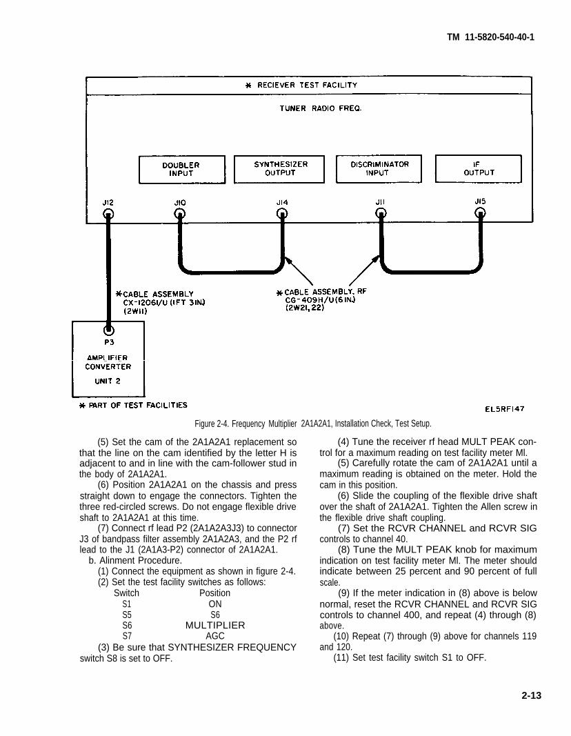
TM 11-5820-540-40-1
Figure 2-4. Frequency Multiplier
(5) Set the cam of the 2A1A2A1 replacement sothat the line on the cam identified by the letter H isadjacent to and in line with the cam-follower stud inthe body of 2A1A2A1.
(6) Position 2A1A2A1 on the chassis and pressstraight down to engage the connectors. Tighten thethree red-circled screws. Do not engage flexible driveshaft to 2A1A2A1 at this time.
(7) Connect rf lead P2 (2A1A2A3J3) to connectorJ3 of bandpass filter assembly 2A1A2A3, and the P2 rflead to the J1 (2A1A3-P2) connector of 2A1A2A1.
b. Alinment Procedure.(1) Connect the equipment as shown in figure 2-4.(2) Set the test facility switches as follows:
Switch PositionS1 ONS5 S6S6 MULTIPLIERS7 AGC
(3) Be sure that SYNTHESIZER FREQUENCYswitch S8 is set to OFF.
2A1A2A1, Installation Check, Test Setup.
(4) Tune the receiver rf head MULT PEAK con-trol for a maximum reading on test facility meter Ml.
(5) Carefully rotate the cam of 2A1A2A1 until amaximum reading is obtained on the meter. Hold thecam in this position.
(6) Slide the coupling of the flexible drive shaftover the shaft of 2A1A2A1. Tighten the Allen screw inthe flexible drive shaft coupling.
(7) Set the RCVR CHANNEL and RCVR SIGcontrols to channel 40.
(8) Tune the MULT PEAK knob for maximumindication on test facility meter Ml. The meter shouldindicate between 25 percent and 90 percent of fullscale.
(9) If the meter indication in (8) above is belownormal, reset the RCVR CHANNEL and RCVR SIGcontrols to channel 400, and repeat (4) through (8)above.
(10) Repeat (7) through (9) above for channels 119and 120.
(11) Set test facility switch S1 to OFF.
2-13

TM 11-5820-540-40-1
2-28. Removal of Connector-Filter Assembly2A1A3
Connector-filter assembly 2A1A3 must be removed inorder to permit replacement of the filter-connectors of2A1A3P3.
a. Place the receiver rf head rear side up and locatefilter-connector assembly 2A1A3.
CAUTION
The two locating pins on the sides of2A1A3P3 are factory alined and shouldnever be loosened or removed
b. Remove the four screws that secure 2A1A3 tochassis XA1A3. Pull 2A1A3 free of the chassis.
c. Replace the fiiter-connectors as required Referto paragraph 2-9 and FO-3 or FO-4 as applicable forreplacement of filter-connectors.
d. If 2A1A3P3 requires replacement unsolder andtag the wires from the pins. Refer to paragraph 2-10and FO-3 or FO-4 as applicable for replacement ofconnectors.
e. Remove the four screws that secure 2A1A3-P3 tothe assembly. Remove 2A1A3P3 from the assembly.
f. Install the replacement 2A1A3P3 and secure itwith the four mounting screws provided
g. Connect and solder the wires removed in d above.h. Place 2A1A3 in position on the chassis and
secure it with the four screws provided
2-29. Replacement of Channel Frequency Indica-tors 2A1A1A1DS1 and 2A1A1A1DS2
a. Removal and Replacement Procedure.(1) Remove control panel 2A1MP2 as described
in paragraph 2-26.(2) Loosen the two setscrews that secure the flex-
ible shaft at the coupling end (fig. 2-5).
NOTE
The two setscrews are held in place by Loc-tite. Melt the Loctite before loosening thescrews.
(3) Remove the four red-circled mounting screw,that secure the defective channel frequency indicatorto the chassis.
(4) Grasp channel indicator and slide it sidewaysto disengage the flexible shaft. Remove the defectivechannel frequency indicator.
(5) Remove the pin through the flexible shaft andremove the flexible shaft.
2-14
(6) Install the flexible shaft on the replacementchannel frequency indicator.
(7) Slip the other end of the flexible shaft over theother shaft, place the channel frequency indicator inposition and secure with the four mounting screws.Tighten the two setscrews.
(8) Using the flexible shaft pin holes as guidesdrill a hole through the channel frequency indicatorshaft end and press the pin through.
b. Channel Frequency Indicator 2A1A1A1DS1(RCVR CHANNEL), Alinement Procedure
(1) Connect the test equipment as shown in C,figure 4-5.
(2) Install the RCVR SIG control knob and rotateit fully clockwise.
(3) Adjust the sweep generator until the receiverfilter response is cetrally displayed on the oscilloscope.
(4) With the air of the markers, adjust the RCVRSIG control until the maximum amplifier (center) ofresponse is tuned to exactly 405 MHz as shown on theoscilloscope.
NOTE
Do not move the RCVR SIG control beyondthis step.
(5) Loosen the two setscrews using using the flexi- ble shaft, turn the tape clockwise until 410 is in linewith the calibration mark
(6) Holding the channel frequency indicator tapefirmly in place tighten the two setscrews to secure theflexible shaft.
(7) Check the alinement of the tape every 20channels down to channel 40. Check to see that theindicated channel and the frequency are in the follow-ing relationship, ± one half inch from the calibrationmark
Channel number = 2 (Frequency (MHz) –200)
Channel NumberFrequency (MHz) = +200)
2
NOTE
When the RCVR SIG control is tuned tochannel 70, set the XMTR DUPL control tochannel 410.
(8) If at any point the alinement is off, adjust theshaft slightly at that frequency and repeat (7) above.
c. Channel Frequency Indicator 2A1A1A1DS2(XMTR DUPL), Alinement Procedure.

TM 11-5820-540-40-1
Figure 2-5. Receiver Rf Head Front View with Front Panel Removed AM-4316/GRC-103(V).
(1) Connect the test equipments shown in C,figure 4-5.
(2) Install the XMTR DUPL control knob androtate it fully clockwise.
(3) Adjust the sweep generator until the transmit-ter filter response is centrally displayed in theoscilloscope.
(4) With the aid of the markers, adjust the XMTRDUPL control until the maximum amplitude (center)of the response is tuned to exactly 405 MHz as shownon the oscilloscope.
NOTE
Do not move the XMTR DUPL controlbeyond this point.
(5) Proceed with b(6) through (8) above.
NOTE
When the XMTR DUPL control is tuned tochannel 70, set the RCVR SIG control tochannel 410.
2-30. Replacement of Channel Frequency Indica-tors 2A1A1DS1 and 2A1A1DS (AM-4316A/GRC-103(V))
a. Removal and Replacement Procedure (fig. 2-6).(1) Remove control panel 2A1MP2 as described
in paragraph 2-26.(2) Remove the three red-circled mounting
screws that secure the defective channel frequencyindicator to the chassis.
(3) Grasp the channel frequency indicator andslide it sideways to disengage the flexible shaft fromthe coupling shaft.
2-15

TM 11-5820-540-40-1
Figure 2-6. Receiver Rf Head Front View With Front Panel Removed AM-4316A/GRC-103(V).
NOTE
The two setscrews in (4) below are held inplace by Loctite. Melt the Loctite beforeloosening the screws.
(4) Loosen the two setscrews securing the flexibleshaft at the frequency indicator.
(5) Install the flexible shaft on replacement chan-nel frequency indicator.
(6) Slip the other end of the flexible shaft over thecoupling shaft. Slide the assembly in position andsecure with three screws.
NOTE
Apply Loctite to flexible shaft setscrewsafter alinement (b. below).
b. Channel Frequency Indicator 2A1A1DS1 (RCVRCHANNEL) Alinement Procedure.
(1) Connect the test equipment as shown in C,figure 4-5.
(2) Install the RCVR SIG control knob and rotateit fully clockwise.
2-16

TM 11-5820-540-40-1
(3) Adjust the sweep generator until the receiverfilter response is centrally displayed on theoscilloscope.
(4) With the aid of the markers, adjust the RCVRSIG control until the maximum amplitude (center) ofresponse is tuned to exactly 405 MHz as shown on theoscilloscope.
NOTE
Do not move the RCVR SIG control beyondthis step.
(5) Loosen the two setscrews, and using the flex-ible shaft turn the tap clockwise until 410 is in line withthe calibration mark.
(6) Holding the channel frequency indicator tapefirmly in place, tighten the two setscrews to secure theflexible shaft.
(7) Check the alinement of the tape every 20channels down to channel 40. Check to see that theindicated channel and the frequency are in the follow-ing relationship:
Channel number = 2 (Frequency (MHz) –200)
Channel NumberFrequency (MHz) = +200)
2
NOTE
When the RCVR SIG control is tuned tochannel 70, set the XMTR DUPL control tochannel 410.
(8) If at any frequency the corresponding channelnumber is more than ½ inch from the calibration mark,adjust the tape slightly and repeat (7) above.
c. Channel Frequency Indicator 2A1A1DS2 (XMTRDUPL) Alinement Procedure.
(1) Connect the test equipment as shown in C,figure 4-5.
(2) Install the XMTR DUPL control knob androtate it fully clockwise.
(3) Adjust the sweep generator until the transmit-ter filter response is centrally displayed in theoscilloscope.
(4) With the aid of the markers, adjust the XMTRDUPL control until the maximum amplitude (center)of the response is tuned to exactly 405 MHz as shownon the oscilloscope.
NOTE
Do not move the XMTR DUPL controlbeyond this point.
(5) Perform procedures given in b(6), (7) and (8)above.
NOTE
When the XMTR DUPL control is tuned tochannel 70, set the RCVR SIG control tochannel 410.
2-31. Replacement of Rotary Switch 5TR1A1S1a. Replacement of switch 5TR1A1S1 is a fourth
order removal. Electrical frequency synthesizer5TR1A2, power supply 5TR1PS1, and alarm control5TR1A3 must be removed first.
b. Remove 5TR1A2, 5TR1PS1 and 5TR1A3 as de-scribed in TM 11-5820-540-30 and chapter 6, TM 11-5820-540-12.
c. On the front panel, loosen the two screws in theswitch control knob, and remove the knob.
d. Locate switch 5TR1A1S1. Loosen and removethe nut that secures 5TR1A1S1 to the front panel.Remove the switch from the mounting hole.
e. Unsolder and tag the wires from switch5TR1A1S1. Refer to FO-5 or FO-6, as applicable.
f. Remove diode CR1 and resistor R3 from thedefective switch. Check the diode and the resistor andinstall them in their correct positions on the replace-ment switch.
g. Refer to FO-5 or FO-6, as applicable and use wireof similar gauge to that on the defective switch to inter-connect all switch contacts necessary to complete cir-cuit, with the exception of wires removed in e above.
h. Position the replacement switch in its mountinghole. Connect and solder the wires, removed in eabove, to their appropriate terminals.
i. Secure the switch with the hexagon nut and thelockwasher.
j Replace the front panel knob and secure it in posi-tion with its two setscrews.
k. Reinstall 5TR1A2, 5TR1PS1, and 5TR1A3 asdescribed in TM 11-5820-540-30 and chapter 6, TM11-5820-540-12.
2-32. Replacement of INPUT Control 5TR1A1R1a. Replacement of INPUT control 5TR1A1R1 is a
third order removal. Electrical frequency synthesizer6TR1A2 and power supply 5TR1PS1 must beremoved first.
2-17

TM 11-5820-540-40-1
b. Remove 5TR1A2 and 5TR1PS1 as described inTM 11-5820-540-30.
c. Locate 5TR1A1AR1 (TM 11-5820-540-30).Unsolder and tag the wires from the defective5TR1A1R1.
d. Loosen the two setscrews in the front panel knoband remove the knob.
e. On the front panel, loosen and remove the hex-agon nut that secures R1, and remove thepotentiometer.
f. Remove resistor R2 from the defective poten-tiometer 5TR1A1R1. Install resistor R2 on the re-placement potentiometer.
g. Install the replacement potentiometer in themounting hole and secure it with the nut provided.
h. Connect and solder the wires removed in c.above.
i. Rotate the potentiometer fully clockwise; replacethe front panel knob in position with the indicator dotopposite the last calibration point at the HIGH end;secure the knob in position with its two setscrews.
j. Replace 5TR1A2 and 4TR1PS1 as described inTM 11-5820-540-30.
2-33. Replacement of Meter 5TR1A1M1a. Replacement of meter 5TR1A1M1 is a third
order removal. Electrical frequency synthesizer5TR1A2 and power supply 5TR1PS1 must beremoved first
b. Remove 5TR1A2 and 5TR1PS1 as described inTM 11-5820-540-30.
c. Locate meter 5TR1A1M1 (TM 11-5820-540-30).Unsolder and tag the wires from the defective meter.
d. Loosen and remove the four mounting screws andnuts and remove the meter.
e. Position the replacement meter and secure withthe four nuts and screws.
f. Connect and solder the wires removed in c. above.g. Replace 5TR1A2 and 5TR1PS1 as described in
TM 11-5820-540-30.
2-34. Replacement of Push Switch 5TR1A1S2a. Place radio transmitter 5TR1 bottom side up and
locate push switch 5TR1A1S2.b. Unsolder and tag the three wires from
5TR1A1S2.c. Remove the nut and washer that secure
5TR1A1S2 to the front panel. Remove 5TR1A1S2.d. Connect terminals 2 and 4 of the replacement
switch together using a short piece of wire of similargauge to that used on the defective switch.
e. Install the new switch and secure it with nut andwasher. Connect and solder the wires removed in b.above.
2-35. Replacement of Rotary Switch 5TR1A1S3a. Place radio transmitter 5TR1 top side up and
locate rotary switch 5TR1A1S3.b. Remove the control knob by unscrewing its two
setscrews.c. Remove the nut and washer securing 5TR1A1S3
to the chassis. Pull the switch free of 5TR1.d. Unsolder and tag the wires from 5TR1A1S3.
Remove 5TR1A1S3.e. Connect and solder the wires removed in d. above
to the replacement switchf. Install the switch in its mounting hole and secure
it with the nut and washer. Replace and secure the con-trol knob.
2-36. Replacement of Circuit Breaker5TR1A1CB1
a Place radio transmitter 5TR1 bottom side up andlocate circuit breaker 5TR1A1CB1.
b. Locate and remove the electrical frequency syn-thesizer 5TR1A2 as described in TM 11-5820-540-30.
c. Remove and discard the insulating tubing on thecircuit breaker 5TR1A1CB1 terminals.
d Unsolder and tag the wires from 5TR1A1CB1terminals.
e. Loosen and remove the hexagonal nut and washerthat secure the circuit breaker to the tint panel.Remove 5TR1A1CB1.
f. Install the replacement circuit breaker in itsmounting hole and secure it with the hexagonal nut andwasher.
g. Remove approximately 1 inch of insulation fromthe ends of the wires to be connected to the circuitbreaker.
h. Place a suitable length of heat shrinkable tubingtype CMC 334-362/3 over each wire.
i. Wrap the wires around both sides of the hook inthe terminals on the circuit breaker. Ensure a goodmechanical connection and that the wires are connect-ed to the correct terminals with regard to LOAD andLINE.
j. Solder the leads to the terminals.k. Position the heat shrinkable tubing on the wires,
over the terminals and using a thermogun, shrink thetubing to fit snugly over the terminals.
l. Replace electrical frequency synthesizer 5TR1A2as described in TM 11-5820-540-30.
2-18

TM 11-5820-540-40-1
2-37. Repair of Electrical Connector Assembly5TR1A1A1 Components
For repair and replacement of connectors and wires inelectrical connector assembly 5TR1A1A1 (FO-5 orFO-6, as applicable). Refer to paragraphs 2-8 and 2-10.
2-38. Removal of Distribution Box 5A2A1 andRadio Interference Filter 5A2FL1
NOTE
Distribution box 5A2A1 must be removedto repair or replace the associated plugsand wiring.
a Remove centrifugal fan 5A2B1 and temperaturecontrol-monitor 5A2A2 (CY-4637NGRC-103 (V) only)(TM 11-5820-540-30).
b. Remove the four screws securing J6(XAR1A2A3P1) to the case.
NOTE
To ensure correct alinement when replacingplug J6, note the order in which the washersor shims are placed under J6.
c. Remove the four screws securing the diaphragmto case partition; slide the diaphragm back on thecable.
d. At the rear of case, remove the eight screwssecuring radio interference filter 5A2FL1 and distribu-tion box 5A2A1 to case.
e. Remove the cable assembly by pulling J6 throughthe slot in the case partition.
f. Replace the cable assembly by feeding J6 and thecable through the slot in the case partition. Positionthe shims and washers under J6 in the order noted inb. above. Secure J6 with the four screws provided.
g. Position radio interference filter 5A2FL1 and dis-tribution box 5A2A1 and secure them with the screwsprovided.
h. Replace and secure the diaphragm to the casepartition.
i. Replace centrifugal fan 5A2B1 and temperaturecontrol monitor 5A2A2 (CY-4637A/GRC-103 (V) only)(TM 11-5820-540-30).
2-39. Replacement of Circuit Card Assembly6AR1A2A2
a. Locate circuit card assembly 6AR1A2A2.Remove the elapsed time indicator by pulling itstraight away from the printed circuit board.
b. Unsolder and tag the wires from connecting pinsE1 through E10.
d.
NOTE
Measure the resistance between TP5 andTP7 of replacement circuit card assembly6AR1A2A2. If gold-plated cavities are usedin the output stage of amplifier 6AR1, thisresistance should be 5.1 ohms ±5%. Ifnickel-plated cavities are used, the resis-tance should be 4.7 ohms ±5%. Ifnecessary, replace resistor R2 with theappropriate resistor, 4.7 ohms (P/N RWR89S4R70DR, NSN 5905-01-009-1878) or5.1 ohms (P/N RWR 69V5R1 or RWR89S5R11FS, NSN 5905-01-173-8930).
Position replacement board 6AR1A2A2 andsecure it with the four screws provided.
e. Connect and resolder the wires removed in b.above.
f. Reinstall the elapsed time indicator in its sockets.
2-40. Removal of Connector-Filter Assembly6AR1A2A3
Connector-filter assembly 6AR1A2A3 must beremoved in order to replace the filter-connectorslocated nearest the 6AR1 chassis, or to repair orreplace P1 (6AR1A2A3). The filter-connectors locatedon the side of 6AR1A2A3 which is not secured to the6AR1 chassis, may be replaced by removing the coverplate on the side of 6AR1A2A3.
a. Locate connector-filter assembly 6AR1A2A3.Measure as accurately as possible and record the dis-tance from front panel 6MP1 to the rear edge of6AR1A2A3.
b. Remove the four red-circled screws that secure6AR1A2A3 to the chassis.
c. Replace connector P1 or the filter-connector asrequired. Refer to paragraph 2-10 for replacement ofconnectors.
d. Replace 6AR1A2A3 and secure it with the fourscrews provided. Before tightening the mountingscrews, position 6AR1A2A3 at the same distancemeasured in a. above; also check the vertical plane ofconnector P1 using a small square and the top edge ofthe 6AR1 chassis as a reference.
2-41. Replacement of Amplifier Assembly6AR1A1 (Fig. 2-7)
a. Removal Procedure.(1) Remove control panel 6MP1 as described in
paragraph 2-45.
2-19

TM 11-5820-540-40-1
Figure 2-7. Amplifier-Frequency MultiplierAM-4320/GRC-103(V), Top View.
2-20
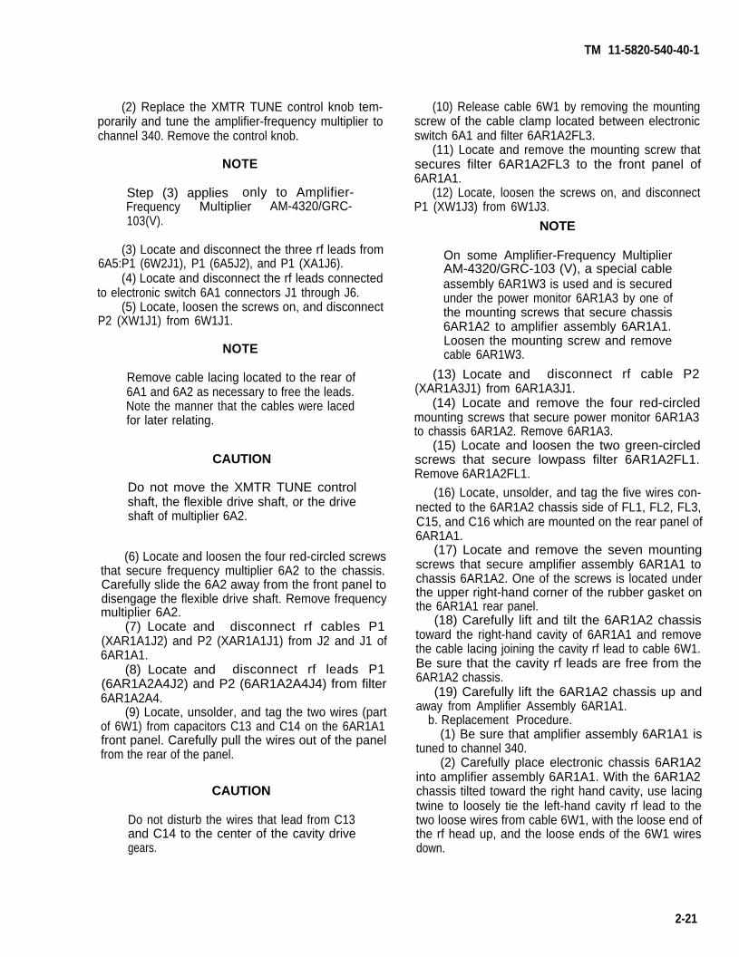
TM 11-5820-540-40-1
(2) Replace the XMTR TUNE control knob tem-porarily and tune the amplifier-frequency multiplier tochannel 340. Remove the control knob.
NOTE
Step (3) applies only to Amplifier-Frequency Multiplier AM-4320/GRC-103(V).
(3) Locate and disconnect the three rf leads from6A5:P1 (6W2J1), P1 (6A5J2), and P1 (XA1J6).
(4) Locate and disconnect the rf leads connectedto electronic switch 6A1 connectors J1 through J6.
(5) Locate, loosen the screws on, and disconnectP2 (XW1J1) from 6W1J1.
NOTE
Remove cable lacing located to the rear of6A1 and 6A2 as necessary to free the leads.Note the manner that the cables were lacedfor later relating.
CAUTION
Do not move the XMTR TUNE controlshaft, the flexible drive shaft, or the driveshaft of multiplier 6A2.
(6) Locate and loosen the four red-circled screwsthat secure frequency multiplier 6A2 to the chassis.Carefully slide the 6A2 away from the front panel todisengage the flexible drive shaft. Remove frequencymultiplier 6A2.
(7) Locate and disconnect rf cables P1(XAR1A1J2) and P2 (XAR1A1J1) from J2 and J1 of6AR1A1.
(8) Locate and disconnect rf leads P1(6AR1A2A4J2) and P2 (6AR1A2A4J4) from filter6AR1A2A4.
(9) Locate, unsolder, and tag the two wires (partof 6W1) from capacitors C13 and C14 on the 6AR1A1front panel. Carefully pull the wires out of the panelfrom the rear of the panel.
CAUTION
Do not disturb the wires that lead from C13and C14 to the center of the cavity drivegears.
(10) Release cable 6W1 by removing the mountingscrew of the cable clamp located between electronicswitch 6A1 and filter 6AR1A2FL3.
(11) Locate and remove the mounting screw thatsecures filter 6AR1A2FL3 to the front panel of6AR1A1.
(12) Locate, loosen the screws on, and disconnectP1 (XW1J3) from 6W1J3.
NOTE
On some Amplifier-Frequency MultiplierAM-4320/GRC-103 (V), a special cableassembly 6AR1W3 is used and is securedunder the power monitor 6AR1A3 by one ofthe mounting screws that secure chassis6AR1A2 to amplifier assembly 6AR1A1.Loosen the mounting screw and removecable 6AR1W3.
(13) Locate and disconnect rf cable P2(XAR1A3J1) from 6AR1A3J1.
(14) Locate and remove the four red-circledmounting screws that secure power monitor 6AR1A3to chassis 6AR1A2. Remove 6AR1A3.
(15) Locate and loosen the two green-circledscrews that secure lowpass filter 6AR1A2FL1.Remove 6AR1A2FL1.
(16) Locate, unsolder, and tag the five wires con-nected to the 6AR1A2 chassis side of FL1, FL2, FL3,C15, and C16 which are mounted on the rear panel of6AR1A1.
(17) Locate and remove the seven mountingscrews that secure amplifier assembly 6AR1A1 tochassis 6AR1A2. One of the screws is located underthe upper right-hand corner of the rubber gasket onthe 6AR1A1 rear panel.
(18) Carefully lift and tilt the 6AR1A2 chassistoward the right-hand cavity of 6AR1A1 and removethe cable lacing joining the cavity rf lead to cable 6W1.Be sure that the cavity rf leads are free from the6AR1A2 chassis.
(19) Carefully lift the 6AR1A2 chassis up andaway from Amplifier Assembly 6AR1A1.
b. Replacement Procedure.(1) Be sure that amplifier assembly 6AR1A1 is
tuned to channel 340.(2) Carefully place electronic chassis 6AR1A2
into amplifier assembly 6AR1A1. With the 6AR1A2chassis tilted toward the right hand cavity, use lacingtwine to loosely tie the left-hand cavity rf lead to thetwo loose wires from cable 6W1, with the loose end ofthe rf head up, and the loose ends of the 6W1 wiresdown.
2-21
TM 11-5820-540-40-1
NOTE
Be sure that the left-hand cavity rf lead isrouted to the rear over the cavity and underthe left side of the 6AR1A2 chassis, that theright hand cavity rf lead is routed upward,that the 6W1 wires are routed downwardbetween, and in front of the cavities, andthat the loose wires at the right rear cornerof the 6AR1A2 chassis are not caught be-tween the chassis and the rear panel ofamplifier assembly 6AR1A1.
(3) Carefully lower the 6AR1A2 chassis until it isalined with the mounting screw holes used to securethe chassis to amplifier assembly 6AR1A1.
(4) Secure the 6AR1A2 chassis to the 6AR1A1amplifier assembly with the eight (or seven, if. cable6AR1W3 is to be used) mounting screws provided.
(5) Reconnect and solder the three wires, discon-nected and tagged in a, (16) above, to the 6AR1A2chassis side of FL1, FL2, and FL3 on the 6AR1A1 rearpanel.
(6) Using suitable lengths of heat shrinkable tub-ing, reconnect, solder, and insulate the wire and jum-per wire to the 6AR1A2 chassis end of C15 and C16 onthe 6AR1A1 rear panel. Use a thermogun to shrink thetubing over the connections and the bodies of Cl 5 andC16.
(7) Install power monitor 6AR1A3 (and cable6AR1W3, if used) to the 6AR1A2 chassis with themounting screws provided. Do not tighten the four red-circled screws at this time.
(8) Reconnect and secure plug P1 (XW1J3) to6W1J3.
(9) Install and secure lowpass filter 6AR1A2FL1with the two green-circled captive screws.
(10) Reconnect rf cable P2 (XAR1A3J1) to6AR1A3J1.
(11) Reconnect rf cable P1 (XAR1A1J2) to6AR1A1J2.
(12) Route the two wires from cable 6W1 throughthe amplifier assembly 6AR1A1 front panel holes pro-vided and reconnect and solder them to C 13 and C 14.Pull the two wires through the lacing (b. (2) above) asrequired to provide a stress loop at C13 and C14.
(13) Resecure cable 6W1 between electronicswitch 6A1 and filter 6AR1A2FL3 with the mountingscrew and cable clamp provided.
(14) Reconnect rf lead P1 (6AR1A2A4J2) to6AR1A2A4J2 and rf lead P2 (6AR1A2A4J4) to6AR1A2A4J4.
(15) Carefully slide frequency multiplier 6A2toward the front panel and engage the flexible driveshaft.
CAUTION
Be sure that the multiplier drive shaft andflexible drive shaft do not rotate.
(16) Position and secure frequency multiplier 6A2with the four red circled captive screws provided.
(17) Reconnect and secure P2 (XW1J1) to 6W1J1.(18) Reconnect the rf leads to electronic switch
6A1 as indicated below
Rf lead Connects toP4 (XA1J1) J1 (6A1)P3 (XA1J2) J2 (6A1)P2 (XA1J3) J3 (6A1)P1 (XA1J4) J4 (6A1)P2 (XA1J5) J5 (6A1)P1 (XA1J6) J6 (6A1)
(19) Reconnect the rf leads from power level con-trol 6A5 (if used), P1 (6W2J1) to 6W2J1 and P1(6A5J2) to 6A5J2.
(20) Using lacing twine, tie the rf leads from elec-tronic switch to cable P2 (XWIJ1), and tie the rf leadsfrom amplifier assembly 6AR1A1 and connectorassembly 6AR1A2A3 together and also to chassis6AR1A2.
(21) Replace control panel 6MP1 as described inparagraph 2-45.
2-42. Replacement of Filter Assembly6AR1A2A4 (Fig. 2-7)
a. Removal Procedure.(1) Separate amplifier assembly 6AR1A1 from
chassis 6AR1A2 as described in paragraph 2-41 a.(1)through (15).
(2) Disconnect rf leads from filter assembly6AR1A2A4; P2(6AR1A2A4J1) and P1(6AR1A2A4J3).
(3) Unsolder and tag the two wires from FL1 andFL2 (6AR1A2A4).
(4) Continue 6AR1A1/6AR1A2 separation asdescribed in paragraph 2-41a (17) and (18).
(5) While chassis 6AR1A2 is tilted (para. 2-41a. (18)), remove the two mounting screws that securefilter assembly 6AR1A2A4. Remove 6AR1A2A4.
2-22

TM 11-5820-540-40-1
b. Replacement Procedure.(1) Install and secure replacement filter assembly
6AR1A2A4 with the two mounting screws provided.(2) Install amplifier assembly 6AR1A1 on chassis
6AR1A2 as described in paragraph 2-41 b. (1) through(4).
(3) Reconnect and solder the two wires to FL1and FL2 of 6AR1A2A4. Connect the two rf leads to6AR1A2A4: P2(6AR1A2A4J1) to J1 and P1(6AR1A2A4J3) to J3.
(4) Continue 6AR1A1/6AR1A2 reassembly asdescribed in paragraph 2-41 b.(7) through (21).
2-43. Replacement of Radio Interference Filter,6AR1A2FL3 (Fig. 2-7)
a. Removal Procedure.(1) Remove control panel 6MP1 as described in
paragraph 2-45.(2) Unsolder and tag the three wires on terminals
E1, E2, and E3 of filter 6AR1A2FL3.(3) Remove the mounting screw that secures filter
6AR1A2FL3 to the front panel of amplifier assembly6AR1A1.
NOTE
If the two nuts securing 6AR1A2FL3 can-not be removed, and replaced, with avail-able tools then amplifier assembly 6AR1A1must be removed as described in paragraph2-41. Replace amplifier 6AR1A1 after re-placing filter 6AR1A2FL3.
(4) Remove the two nuts and washers that securefalter 6AR1A2FL3 to chassis 6AR1A2. Remove6AR1A2FL3.
b. Replacement Procedure.(1) Install and secure filter 6AR1A2FL3 with the
mounting screw and two nuts and washers provided.(2) Place a suitable length of heat shrinkable tub-
ing over each of the three wires.(3) Reconnect and solder the wires to E1, E2, and
E3 of filter 6AR1A2FL3.(4) Position the shrinkable tubing to cover the
connections and terminals and use a thermogun toshrink the tubing as positioned.
(5) Replace control panel 6MP1 as described inparagraph 2-45.
2-44. Replacement of Channel Frequency Indica-tor6AR1A1DS1
a. Removal and Replacement Procedure.(1) Remove control panel 6MP1 as described in
paragraph 2-45.(2) Remove the red-circled mounting screws that
secure the defective channel frequency indicator to thechassis.
(3) Grasp the channel frequency indicator andslide the unit sideways to disengage the flexible shaft.Remove the defective channel frequency indicator.
(4) Remove the flexible shaft from the defectivechannel frequency indicator.
NOTE
The two setscrews in the flexible shaft areheld in place with Loctite. Melt the Loctitebefore loosening the setscrews.
(5) Install the flexible shaft to the replacementchannel frequency indicator.
(6) Slip the other end of the flexible shaft over thehexagonal shaft. Place the channel frequency indicatorin position on the chassis and secure it with the mount-ing screws.
(7) Position the flexible shaft equally between thechannel frequency indicator and the hexagonal shaft.Secure the flexible shaft to the channel frequencyindicator with the two setscrews. Lock the setscrews asdescribed in paragraph 2-13.
(8) Loosen the mounting screws, remove thecharnel frequency indicator from the chassis and pro-ceed with alinement procedures described in b. below.
b. Alinement Procedure.(1) Connect plug P1 (6W1J2) at the end of
control-indicator 6A3 cable to connector 6W1J1.(2) Set the XMTR CHANNEL control to channel
320.(3) Connect the transmitter rf head to the test
facility as shown in figure 4-26.
(4) Set the test facility switches as follows:
SwitchSwitch position Normal indication
S1 ONS20 S12S12 OSC Test facility meter M1 indicates between
25% and 90% of full scale deflection.
(5) Check the 115 Vac on the power supply (partof the accessory kit); adjust if required.
2-23
TM 11-5820-540-40-1
(6) Set the test facility switches as follows:
SwitchSwitch position
S12 DBLR
S12 MULT
S13 ON
(7) Recheckjust if required
Normal indication
M1 indicates between 25% and 90% of fullscaleM1 indicates between 25% and 90% of fullscale
115 Vac on the power supply; read-
(8) Install the XMTR TUNE control knob andtune for maximum ouput at 370 MHz.
(9) Set test facility switch S12 to the DRIVERposition. Push in the PWR OUT PEAK control andtune for maximum indication on meter Ml. Meter Mlshould indicate between 25 percent and 90 percent offull scale.
(10) Set test facility switch S12 to the PWR OUTposition. Pull out the PWR OUT PEAK control andtune for maximum indication on meter Ml. The metershould indicate between 25 percent and 90 percent offull scale.
(11) Set test facility switch S1 to OFF.
NOTE
Do not move the XMTR TURN controlafter the power amplifier has been peaked
(12) On the replacement channel frequencyindicator 6AR1A1DS1, rotate the flexible shaft clock-wise until 320 is in line with the calibration mark(notch) on the frame.
(13) Hold the channel frequency indicator tapefirmly and slip the flexible shaft over the hexagonal-ended shaft Secure 6AR1A1DS1 to the chassis withthe mounting screws provided
NOTE
The flexible shaft may have to be movedslightly while installing the assembly to fitthe hexagonal-ended shaft
(14) Set test facility switch S1 to ON. Readjust theXMTR TUNE and PWR OUT PEAK controls formaximum output. Check to see that the channel fre-quency indicator number 320 is not more than one-eighth inch above or below the calibration mark(notch) on 6AR1A1DS1. If necessary, remove6AR1A1DSl and readjust the tape position.
(15) Set the XMTR TUNE and XMTR CHAN-NEL controls to indicate channel 40 in line with thecalibration mark.
(16) Set test facility switch S12 to the DRIVERposition. On the transmitter rf head, push the PWROUT PEAK control and tune for maximum meterindication on test facility meter M1.
(17) Set switch S12 to PWR OUT. Pull out thePWR OUT PEAK control and tune for maximum read-ing on meter M1. The level measured by the wattmetershould be greater than 35 watts.
(18) Repeat (15) through (17) above for channels100,200, and 410. Check to see that the number of thechannel being checked is not more than ½-inch aboveor below the calibration mark
(19) Restore the test facility switches to normaland disconnect plug P1 (6W1J2) from connector6W1J1.
(20) Install control panel 6MP1 as described inparagraph 2-45.
2-45. Replacement of Control Panel 6MP1a Removal Procedure.
(1) Remove the XMTR TUNE and the PWROUT PEAK control knobs.
(2) Remove the hexagon nut and washer from thePWR OUT connector.
(3) Loosen the two screws that secure plug P1(6W1J2) to its mating connector 6W1J2 (TM 11-5820-540-30) and disconnect the plug.
(4) Loosen and remove the six mounting screwslocated at the rear of the panel and remove controlpanel 6MP1.
b. Replacement Procedure.(1) Loosen, but do not remove, the four red-
circled screws that secure Power Monitor 6AR1A3 tochassis 6AR1A2.
(2) Place control panel 6MP1 in position andsecure it with the six mounting screws provided
(3) Connect plug P1 (6W1J2) of the control-indicator 6A3 cable to connector 6W1J2. Secure theplug in position with the two screws provided
(4) Replace and secure the nut and washer to thePWR OUT connector. Tighten the power monitor6AR1A3 mounting screws. Install the XMTR TUNEand PWR OUT PEAK control panel knobs.
2-46. Replacement of Order Wire (Unit 9)
For removal and replacement procedures on orderwire, see section VI (para. 2-96).
2-24

TM 11-5820-540-40-1
Section Ill. REMOVAL AND REPLACEMENT PROCEDURES -
BAND II RF HEAD
2-47. Replacement of Channel Frequency Indica-tor 33A1A1DS1 or 33A1A1DS2
a. Remove front panel 33A6 as described in para-graph 2-55.
b. Remove the red-circled mounting screws that se-cure the defective channel frequency indicator(33A1A1DS1 or 33A1A1DS2 fig. 4-62) to the chassis.
c. Grasp channel frequency indicator and slide itsideways to disengage the flexible shaft. Remove thedefective channel frequency indicator.
d. Remove the pin through the flexible shaft andremove the flexible shaft from the defective channelfrequency indicator.
e. Install the flexible shaft on the replacement chan-nel frequency indicator and secure with a setscrew.
f. Install the RCVR SIG control knob if 33 Al Al-DS1 is being replaced, or XMTR CHANNEL controlknob if 33A1A1DS2 is being replaced.
g. Turn the control knob clockwise to the stopposition.
h. Turn the flexible shaft, on the replacement chan-nel frequency indicator, clockwise until the start posi-tion, indicated by an arrow head and the letter “S,” isalined with the calibration mark. The calibration markis a notch centrally located on the front edge of theunit’s frame.
i. Place the channel frequency indicator in positionand slip the hexagonal recessed end of the flexibleshaft over the coupling shaft (fig. 4-62).
j. If the stop position of the channel control and thestart position on the tape do not coincide, proceed asfollows:
(1) Loosen the setscrew in the flexible shaft(2) Ensure that the channel control is turned fully
clockwise.(3) Adjust the tape to realine the start position as
in step h. above.(4) Retighten the setscrew securing the flexible
shaft.k. Remove the channel frequency indicator. Using
the guide holes in the flexible shaft drill a hole throughthe channel frequency indicator shaft Press a pinthrough both shafts. Remove the setscrew.
l. Reinstall the channel frequency indicator and se-cure in position with the mounting screws.
2-48. Replacement of Connector-Filter Assembly33A1W1A1
a. Place the receiver rf head rear side up and locateconnector-filter assembly 33A1W1A1 (fig. 2-8).
CAUTION
The two locating pins on the sides of33A1WIA1 are factory alined and shouldnever be loosened or removed.
b. Remove the four screws that secure 33A1W1A1to the chassis. Pull 33A1W1 Al free of the chassis.
c. Replace filter-connectors as required. Refer toparagraph 2-9 and FO-7 for replacement of filter-connectors. If the existing plug 33A1W1A1P1 is to beused, proceed to step h. below.
d. If 33A1W1A1P1 required replacement, unsolderand tag the wires from the pins.
e. Remove the four screws that secure33A1W1A1P1 to the assembly remove 33A1W1A1P1from the assembly.
f. Install the replacement 33A1W1A1P1 and secureit with the four mounting screws provided.
g. Connect and solder the wires removed in d.above. Refer to paragraph 2-10 and FO-7 forconnections.
h. Place 33A1W1A1 in position on the chassis andsecure it with the four screws removed in b. above.
2-49. Replacement of Terminal Board33A1W1TB1
a. Remove intermediate frequency amplifier33AR1, frequency mixer 33A7, lowpass filter 33FL1,signal level control monitor 33A5 (TM 11-5820-540-30), and power supply 33PS1 (if used) (TM 11-5820-540-12).
b. Locate and remove the mounting screws ofchassis connectors 33A1W1J8 and 33A1W1J9. Pushthese connectors down through the holes provided inthe bottom support
c. Remove the six mounting screws of the bottomsupport Remove the bottom support
d. Remove the two mounting screws that secure thedefective terminal board to the bottom support.
2-25

TM 11-5820-540-40-1
Figure 2-8. Band II Receiver Rf Head Top and Left-Hand Side View.
2-26

TM 11-5820-540-40-1
e. Unsolder and tag the wires attached to the ter-minal board 33A1W1TB1.
f. Solder the wires to the replacement terminalboard. Refer to wiring diagram FO-7 if necessary.
g. Mount the replacement terminal board in its posi-tion and tighten the two mounting screws.
h. Place the bottom support in its position and pullthe connectors 33A1W1J8 and 33A1W1J9 up throughthe holes provided. Secure the bottom support with sixmounting screws.
i. Secure the two chassis connectors 33A1W1J8and 33A1W1J9 to the bottom support with the mount-ing screws provided.
j. Replace 33AR1, 33A7, 33FL1, and 33A5 (TM 11-5820-540-30).
k. Replace 33PS1 (if used) (TM 11-5820-540-12).
2-50. Replacement of Speed Decreaser GearAssembly 33A1MP1
a. Loosen the screws in the MULT PEAK knob onthe front panel. Remove the knob.
b. Loosen the two screws in the coupling shaft thatsecure the speed decreaser gear assembly shaft
c. Place the receiver rf head right side up and locatethe speed decreaser gear assembly 33A1MP1.Unscrew the three red-circled screws and remove thespeed decreaser gear assembly 33A1MP1.
d. To install replacement speed decreaser gearassembly 33A1MP1, rotate the MULT PEAK shaftuntil the speed decreaser gear shaft will fit into thecoupling shaft when speed decreaser gear assembly33A1MP1 is placed in position over the three mount-ing holes. The MULT PEAK shaft should project fromthe hole in the front panel.
e. Tighten the three red-circled mounting screws.f. Tighten the two screws in the coupling shaftg. Replace and secure the MULT PEAK knob.h Aline the amplifier-converter unit 33 as de-
scribed in paragraph 4-19 d.
NOTE
c. Locate and loosen the two screws that secure P3(33A1W1J7) (fig. 2-8) to chassis connector33A1W1J7. Disconnect P2 (33A1W1J7) plug.
d. If the flexible type coupling shaft is used, loosenthe two setscrews that secure it to the multiplier groupdrive shaft. Apply heat to soften the sealant on thesetscrews.
e. Place the receiver rf head right side up. Locateand unscrew four red-circled mounting screws securingthe multiplier group 33A2.
f. Place the receiver rf head left side up. Locate andunscrew the remaining two red-circled mountingscrews securing the multiplier group 33A2.
NOTE
Be sure that the rigid rf lead is not damagedor bent while removing or installing 33A2.
g. Lift the frequency multiplier group 33A2 straightup.
h. To install replacement frequency multipliergroup 33A2, loosen the clamp on gear A (fig. 4-62) anddisengage gear A from the speed decreaser drive gear.Lower the multiplier group straight down into itsmounting position after rotating the MULT PEAKcontrol so that the multiplier group drive shaft fits intothe coupling shaft.
i Replace and tighten the two red-circled screwssecuring the module to the left side of the chassis.Tighten the setscrews in the coupling shaft, if the flex-ible type coupler is used. Replace and tighten the fourremaining red-circled screws securing the module tothe right side of the chassis.
j. Connect rf leads P1 (33A1W1A1J2) and P2(33W7J1) to their respective connectors.
k. Connect plug P2 (33A1W1J7) to chassis connec-tor 33A1W1J7 and secure in position with the screwsprovided.
l. Realine the band II receiver rf head as describedinparagraph 4-19 d.(1).
It should not be necessary to perform thealinement procedures of the voltage controlassembly 33A1A2.
2-51. Replacement of Frequency MultiplierGroup 33A2
a. Place the receiver rf head upright and locate themultiplier group 33A2 (fig. 2-10).
b. Disconnect rf leads P1 (33 A1W1A1J2) and P2(33W7J1) (fig. 2-8) from their respective connectors.
2-52. Replacement of Frequency Multiplier33A2A1
a. Set the receiver rf head RCVR SIG control tochannel 390.
b. Turn the MULT PEAK control so that the redmark on gear B (fig. 4-65) coincides with the red markon the casting.
c. Locate and loosen, but do not disconnect, rf leadsP2 (33A2A2J1) and P2 (33A2FL1J1).
2-27

TM 11-5820-540-40-1
d. Locate and disconnect rf leads P3 (33A2A1J1)and P1 (33A2A1J2) from their respective connectorson frequency multiplier 33A2A1. Be sure that the rfleads are not damaged or bent.
e. Locate and loosen the three green-circled screwsthat secure frequency multiplier 33A2A2. Remove33A2A2.
f. Locate and loosen the three red-circled screwsthat secure frequency multiplier 33A2A1.
g. Move frequency multiplier 33A2A1 toward therear of the rf head and lift the module out, carefullydisengaging the drive gears and disconnecting thepower connector located under the module.
h. To install the replacement frequency multiplier33A2A1, adjust the module drive shaft so that the redmark on the gear coincides with the red mark on themodule casting.
i. Position frequency multiplier 33A2A1 to the rearof its mounting holes and then move the module for-ward, carefully engaging the gears and the connectorlocated under the module. Tighten the three red-circled mounting screws.
j. Replace and secure frequency multiplier 33A2A2with the mounting screws provided
k. Carefully connect rf leads P3 (33A2A1J1) to J1of 33A2A1 and P1 (33A2A1J2) to J2 of 33A2A1.Tighten the connectors at both ends of the rf leads.
l. Aline multiplier group 33A2 as described inparagraph 4-33 b.(3), with the following exceptions:
(1) Connect receiver test facility J12 to rf headconnector 33A1W1A1P1 with cable assembly CX-12061 (2W11).
(2) Disconnect P2 (33A7J2) from 33A7J2 andconnect the test setup, shown in figure 4-64 as con-nected to 33 A2J2, to P2 (33A7J2).
(3) Disconnect PI (33A1W1A1J2) from33A1W1A1J2.
(4) Use MULT PEAK control, and RCVR SIGcontrol as needed, to turn shaft C (fig. 4-65).
(5) Reconnect P2 (33A7J2) to 33A7J2 and P1(33A1W1A1J2) to 33A1W1A1J2 after alinement of33A2.
m. Realine the local oscillator to the rf head as de-scribed in paragraph 4-19 d. (1).
2-53. Replacement of Bandpass Filter 33A2FL1and Cable Assembly 33A2FL1W1Components
a. Replacement of Cable Assembly 33A2FL1W1Components.
(1) Remove frequency multiplier 33A2A1 as de-scribed in paragraph 2-52 a. through g.
(2) Tag the wires, unsolder, replace, and resolderthe component(s) as described in the appropriate sec-tions of paragraphs 2-7, 2-8, 2-10, and 2-11. Refer toFO-7 for cable 33A2FL1W1 connections.
(3) Replace frequency multiplier 33A2A1 as de-scribed in paragraph 2-52 h. through m.
b. Removal of Bandpass Filter 33A2FL1.(1) Remove frequency multiplier 33A2A1 as de-
scribed in paragraph 2-52 a through g.(2) Remove bandpass filter 33A2FL1 as de-
scribed for multiplier group 33A2 in paragraph 2-51 athrough g.
c. Replacement of Bandpass Filter 33A2FL1.(1) Position frequency multiplier 33A2A1 to
properly engage its connector and gear and press it inplace. Secure 33A2A1 with the mounting screwsprovided
(2) Install and secure frequency multiplier33A2A2 with the mounting screws provided.
(3) Connect plug P1 (33A2A1J2) to J2 of33A2A1, plug P2 (33A2A2J1) (part of 33A2W1) to J1of 33A2A2, and plug P3 (33A2A1J1) (part of33A2W1) to J1 of 33A2A1.
(4) Aline and check assembled multiplier group33A2 as described in paragraph 4-23 b. (3).
(5) Reinstall multiplier group 33A2 as describedin paragraph 2-51 h. through l.
2-54. Replacement of Rf power Monitor 33A3
a. Remove control panel 33A6 as described inparagraph 2-55.
b. Place the receiver rf head front side up and locatethe rf power monitor 33A3 (fig. 4-62).
c. Locate and loosen the two screws that secureP1(33A1W1J3) to 33A1W1J3 (fig. 4-62). RemoveP1(33A1W1J3) plug.
d. Loosen, but do not disconnect plug P1(33A3J2).e. Locate and remove the four mounting screws that
secure the rf power monitor 33A3 to the chassis.f. Disconnect P2(33A3J1) and P1(33A3J2) (fig. 4-
62) from the J1 and J2 connectors of 33A3.g. Lift the rf power monitor complete with cable
from the chassis.h. To install the replacement module, position 33A3
in its place and loosely connect rf lead P1(33A3J2) toJ2 of 33A3.
i Secure power monitor 33A3 in position with thefour mounting screws.
j. Connect and secure P1(33A3J2) rf lead to con-nector J2 and P2(33A3J1) rf lead to connector J1 of rfpower monitor 33A3.
k. Connect P1(33A1W1J3) plug to 33A1W1J3chassis connector. Secure in position with screwsprovided.
2-28
TM 11-5820-540-40-1
l. Replace control panel 33A6 as described inparagraph 2-55.
2-55. Replacement of Control Panel 33A6
a. Place the receiver rf head top side up and locatecontrol panel 33A6.
b. Locate and loosen the two screws that secureP 1 ( 3 3 A 1 W 1 J 5 ) t o 33 A1W1J5. RemoveP1(33A1W1J5).
c. Loosen the screws in the MULT PEAK, RCVRSIG and XMTR DUPL control panel knobs andremove the knobs.
d. Using a socket wrench, remove the two nuts andwashers that secure the ANT. and FROM XMTR con-nectors to the control panel. Note the manner in whichcable P1(33A1W1J5) is routed to control indicator33A4.
e. Loosen the eight mounting screws that securecontrol panel 33A6 to the chassis. Remove the controlpanel. Be sure that the ANT. and FROM XMTR con-nectors are free from the control panel.
f. To reinstall 33A6, place the control panel over theANT. and FROM XMTR connectors and position thepanel on the chassis so that the guide pins and mount-ing holes are properly alined.
g. Secure control panel 33A6 with the eight mount-ing screws. Secure the ANT. and FROM XMTR con-nectors with the nuts and washers provided.
h. Replace and secure the MULT PEAK, RCVRSIG and XMTR DUPL control knobs. Make sure thatthe backs of the knobs clear the control panel by 1/8
(3) Locate and remove the strap and two screwsthat secure rf lead 37W1 to chassis 37AR1A1.
(4) Locate and loosen P2(37AR1AR1J1). Allow rflead 37W1 to swing away from multiplier 37A1.
(5) Loosen the four red-circled screws that securethe frequency multiplier 37A1 to the chassis. Pull37A1 straight up, carefully disengagingP1 (37AR1A1W1J2) from the chassis connector37AR1A1W1J2. Slide 37A1 away from the front panelto disengage the flexible shaft.
NOTE
The 37A1 replacement module is shippedwith its shaft clamped to channel 1010 (705MHz). Remove the clamp carefully to avoiddisturbing the shaft position.
(6) Lower the 37A1 replacement module intoposition carefully engaging the flexible shaft to itsdrive mechanism. Carefully engageP1(37AR1A1W1J2) to chassis connector37AR1A1W1J2.
(7) Secure 37A1 to the chassis with the fourscrews provided.
(8) Reconnect rf leads 37AR1A1W1A1P2 andP1(37A1J2) to 37A1J1 and 37A1J2, respectively.
(9) Tighten rf lead P2(37AR1AR1J1) on J1 ofamplifier 37AR1AR1.
(10) Replace the strap and two screws removed in(3) above.
inch.i Route cable P1(33A1W1J5) as noted in b. above c. Alinement Check.
and connect it to 33A1W1J5 and secure the plug in (1) Connect the equipment as shown in figure 2-9.
position with the screws. (2) Direct cooling air from the AIR OUTLET ofthe transmitter test facility to the rear of the unit under
2-56. Replacement of Frequency Multiplier 37A1 test.(3) With the XMTR TUNE and XMTR CHAN-
a Test Equipment and Material Required. NEL controls set to channel 1010, set the test facility
Equipment Common name switches as follows:
Test Facility, Transmitter Transmitter test facilityTS-2866(V)2/GRM-95(V)2. Switch
Accessory Kit, Test Facilities Accessory kit Switch positionSet MK-1173(V)2/GRM-95(V)2.
Wattmeter AN/USM-298 Wattmeter S1 ONS13 ON
Normal indication
b. Removal and Replacement Procedure. S20 S12S12 OSC
(1) Set the transmitter rf head XMTR TUNE andMeter Ml indicates between 20% and
90% of full scale.XMTR CHANNEL controls to channel 1010.
(2) Place the transmitter rf head upright andlocate frequency multiplier 37A1. Disconnect the (4) Turn test facility switch S12 to PWR OUT37AR1A1W1A1P2 and P1(37A1J2) rf leads connect- and adjust PWR OUT PEAK control for maximumed to frequency multiplier 37A1. indication on the test facility meter Ml.
2-29

TM 11-5820-540-40-1
FigUre 2-9. Frequency Multiplier 37A1, Alinement Check, Test Setup.
(5) Adjust the XMTR TUNE and PWR OUTPEAK controls for maximum indication on thewattmeter. The wattmeter should indicate at least 25watts. The XMTR TUNE channel indication shouldbe within 0.5 inch of the centerline of the displaywindow.
(6) Repeat steps (4) and (5) above with theXMTR CHANNEL and XMTR TUNE controls set tochannels 390, 400, 480, 560, 640, 720, 760, 800, 880,960 and 1000 in turn.
(7) Select the channel giving the highest errorabove ±0.5 inch on the XMTR TUNE charnelindicator tape. Set the XMTR CHANNEL control tothe channel selected.
(8) Set the test facility switch S12 to MULT andtune the XMTR TUNE control for maximum indica-tion on the test facility meter M1.
(9) Set the test facility switch S1 to OFF andremove 37A1 as described in steps b.(2) through (5)above.
(10) Turn the XMTR TUNE control until thechannel selected in step (7) above is within 0.5 inch ofthe display window center line.
(11) Repeat steps b.(6) through (10) to reinstall37A1.
(12) Set the test facility switch S1 to ON andrepeat step (6) above. Repeat steps (7) through (11)above as necessary.
2-57. Replacement of Radio Interference Filter37AR1A1FL2
a. Place the transmitter rf head rightside up andlocate radio interference filter 37AR1A1FL2.
b. Remove the two screws securing the red coverplate to the filter remove the red cover plate.
c. Unsolder and tag the three wires from connectingpins E1, E2, and E3 of filter 37AR1A1FL2.
d. Remove the two screws securing the radio inter-ference filter and remove the filter.
2-30

TM 11-5820-540-40-1
e. Position the replacement filter and secure it withthe two screws removed in d. above.
f. Remove the two screws securing the red coverplate on the replacement filter remove the red coverplate.
g. Place a suitable length of heat shrinkable tubingtype CMC 334-362/3 over each wire to be connectedto E1, E2, and E3 of 33 AR1A1FL2.
h. Wrap the wires around both sides of the hook ter-minals on the radio interference falter. Ensure a goodmechanical connection and solder leads to theterminals.
i. Position the heat shrinkable tubing on the wiresover the soldered terminals. Use a thermogun to shrinkthe tubing over the terminals.
j. Replace the red cover plate and secure with thescrews removed in/l above.
2-58. Replacement of Control Panel 37MP1
a. Removal Procedure.(1) Remove the XMTR TUNE and the PWR
OUT PEAK control knobs.(2) Remove the hexagon nut and the flat washer
from the PWR OUT connector.(3) Loosen the two screws that secure plug
P1(37AR1A1W1J3) to i ts mating connector37AR1 A1W1J3 and disconnect the plug.
(4) Loosen and remove the six green-circledmounting screws and washers located at the rear of thecontrol panel, and remove the control panel.
NOTE
Pull the panel forward from the rf head torelease it from the guiding pin.
b. Replacement Procedure.(1) Place the control panel in position and press
to slide home the guiding pin.
NOTE
It may be necessary toscrews holding the
loosen the fourpower monitor
37AR1A2 in position. Do not retightenscrews at this time.
(2) Secure the control panel to the chassis usingthe six screws removed in a. (4) above.
trol(3) Connect Pl(37AR1A1WlJ3) of the the con-indicator 37A2 to connector 37AR1A1W1J3 and
secure the plug in position with the two screwsprovided.
(4) Replace and secure the nut and washer to thePWR OUT connector. Tighten the power monitor37AR1A2 mounting screws.
(5) Install the XMTR TUNE and PWR OUTPEAK control panel knobs.
2-59. Replacement of Channel Frequency Indica-tor 37AR1AR1DSl
a. Removal and Replacement Procedure.(1) Remove control panel 37MP1 as described in
paragraph 2-58.(2) Reconnect the XMTR TUNE knob to the
shaft of the XMTR TUNE control. Turn the XMTRTUNE control fully clockwise to the stop.
(3) Locate the channel frequency indicator (fig. 2-10). Remove the three red-circled screws that securethe channel frequency indicator to the chassis.
(4) Grasp the channel frequency indicator andslide it sideways to disengage the flexible shaft fromthe hexagonal shaft Remove the defective channel fre-quency indicator.
(5) Remove the flexible shaft from the defectivechannel frequency indicator by removing the straightpin through the end of the shaft and loosening the twosetscrews (if installed).
(6) Slide the flexible shaft on to the hexagonalshaft
(7) Turn the replacement channel frequencyindicator until the white cross hatch (above charnel1010) on the tape is alined with the calibration mark(notch) on the frame.
(8) Slide the replacement channel frequencyindicator sideways to connect the shaft of the channelfrequency indicator to the free end of the flexible shaft
(9) Secure the channel frequency indicator withthe three screws removed in a. (3) above.
(10) Position the flexiable shaft midway betweenthe channel frequency indicator and the hexagonalshaft Secure the flexible shaft to the channel fre-quency indicator using setscrews. (Do not drill and pinflexible shaft in position at this time.)
b. Channel Alinement Check and Adjustment(1) Connect control indicator plug
P1 (37AR1A1W1J3) on the control panel to connector37AR1A1W1J3 on the transmitter rf head chassis.
(2) Connect the test equipment as shown in figure2-9.
2-31

TM 11-5820-540-40-1
Figure 2-10. Band II Transmitter Rf Head Front View, Front Panel Removed.
2-32

TM 11-5820-540-40-1
(3) Turn XMTR CHANNEL control to channel390 (395 MHz).
(4) Turn XMTR TUNE control to channel 390.(5) Set test facility switches S1 to ON, S20 to
S12, S12 to OSC, and S13 to ON.(6) Install the PWR OUT PEAK knob to the shaft
of the PWR OUT PEAK control.(7) Adjust the PWR OUT PEAK control two-
thirds of a rotation away from the fully clockwiseposition.
(8) Adjust the XMTR TUNE control for a max-imum power indication on the wattmeter.
(9) Check that the PWR OUT PEAK control iscapable of tuning the power output both sides of thepeak power indication. Readjust the XMTR TUNEand the PWR OUT PEAK control, if necessary, toobtain this capability.
(10) Check the channel frequency indicator; chan-nel 390 should not be more the 1/8 inch above or belowthe calibration mark (notch) on 37AR1AR1DS1.
CAUTION
Ensure that the flexible shaft does notmove during the adjustment in (11) below.
(11) If the channel frequency indication is morethan 1/8 inch removed from the calibration mark loosenthe two setscrews holding the flexible shaft to thechannel frequency indicator and adjust the channelfrequency indicator until the channel indication (390)is alined with the calibration mark.
(12) Tighten the setscrews to secure the flexibleshaft to the channel frequency indicator.
(13) Check the alinement at channels 450, 550,650, 750,850 and 1000 as shown in steps (3), (4), (8),and (9) above. If the channel number of the charnelbeing checked is more than ½ inch above or below thecalibration mark, slightly readjust as in (11) and (12)above.
(14) Drill the shaft of the channel frequencyindicator shaft using the pilot hole provided. Pin theflexible shaft.
(15) Remove the XMTR TUNE and PWR OUTPEAK knobs and disconnect P1(37AR1A1W1J3)from connector 37 AR1A1W1J3. Install control panel37MP1 as described in paragraph 2-58.
2-60. Replacement of Resistor Assembly37AR1A1A2
a. Turn transmitter rf head left side up and locateresistor assembly 37AR1A1A2.
b. Unsolder and tag leads connected to terminal E 1.
c. Remove the two green-circled screws that securethe resistor assembly to the chassis; remove the resis-tor assembly.
d. Secure the replacement resistor assembly to thechassis using the two screws removed inc. above.
e. Place a suitable length of heat shrinkable tubingtype CMC 334-362/3 over the wires removed in b.above.
f. Connect and solder the wires to the terminal E1.Position the heat shrinkable tubing on the wires overthe terminal. Use a thermogun to shrink the tubingover the terminal.
2-61. Replacement of Connector-Filter Assembly37AR1A1W1A1
Connector-filter 37AR1A1W1A1 must be removed inorder to replace the filters next to the 37AR1 chassis,or to repair or replace 37AR1A1W1A1P1. The filterslocated on the side not secured to the chassis may bereplaced by removing the side cover plate of37 AR1A1W1A1.
a. Place the transmitter rf head 37 right side up andlocate the voltage regulator assembly 37 AR1A1A1.Loosen the four green-circled screws on the voltagergulator assembly and remove the voltage regulatorassembly.
b. Locate the connector-filter assembly37AR1A1W1A1. Measure as accurately as possibleand record the distance from control panel 37MP1 tothe rear edge of 37 AR1A1W1A1.
c. Remove the four red-circled screws that securethe 37 AR1A1W1A1 to the chassis and move theconnector-filter carefully away from the chassis.
d. If the connector-filter assembly is to be changed,unsolder and tag the wires connected to the filters FL1to FL46. Remove the defective connector-filterassembly and resolder the tagged wires to the replace-ment connector-falter assembly.
e. If a single filter is to be changed, unsolder thewires from both sides of the filter and remove thedefective filter. Install the replacement filter and con-nect and solder the wires removed from the defectivefilter.
f. Refer to paragraph 2-10 for replacement ofconnector.
g. Replace connector-falter assembly37AR1A1W1A1 using the four mounting screwsremoved in c. above. Position 37 AR1A1W1 at thesame distance as measured in b. above, and check thevertical plane of connector P1 using a small square andthe top edge of the 37AR1 chassis as a reference.Tighten the four mounting screws.
h. Reinstall the voltage regulator assembly37AR1A1A1 and tighten the 4 mounting screws.
2-33

TM 11-5820-540-40-1
Section IV. REMOVAL AND REPLACEMENT PROCEDURES -
BAND Ill
2-62. Replacement of Channel Frequency Indica-tor 34A1A1DS1 or 34A1A1DS2
a. Remove “control panel 34A6 as described inparagraph 2-70.
b. Remove the three red-circled mounting screwsthat secure the defective channel frequency indicator34 A1A1DS1 or 34A1A1DS2 (fig. 4-62) to the chassis.
c. Grasp channel indicator and slide it sideways todisengage the flexible shaft. Remove the defectivechannel frequency indicator.
d. Remove the pin through the flexible shaft andremove the flexible shaft from the defective channelfrequency indicator.
e. Install the flexible shaft on the replacement chan-nel frequency indicator and secure with a setscrew.
f. Install the RCVR SIG control knob if34A1A1DS1 is being replaced, or the XMTR CHAN-NEL control knob if 34A1A1DS2 is being replaced.
g. Turn the control knob fully clockwise to the stopposition.
h. Turn the flexible shaft, on the replacement chan-nel frequency indicator, clockwise until the start posi-tion, indicated by an arrow head and the letters “RS”for 34A1A1DS1 and “TS” for 34A1A1DS2, is alinedwith the calibration mark The calibration mark is anotch centrally located on the front edge of the unit’sframe.
i. Place the channel frequency indicator in positionand slip the hexagonal recessed end of the flexibleshaft over the associated coupling shaft (fig. 4-62).
j. If the stop position of the channel control and thestart position on the tape do not coincide, proceed asfollows:
(1) Loosen the setscrew in the flexible shaft(2) Ensure that the channel control is turned fully
clockwise.(3) Adjust the tape to realine the start position as
in step h. above.(4) Retighten the setscrew securing the flexible
shaft.k. Remove the channel frequency indicator. Using
the guide holes in the flexible shaft drill a hole throughthe channel frequency indicator shaft. Press a pinthrough both shafts. Remove the setscrew.
l. Reinstall the channel frequency indicator andsecure in position with the three mounting screws.
RF HEADS
2-63. Replacement of Connector-Filter Assembly34A1W1A1
a Place the receiver rf head rear side up and locateconnector filter assembly 34A1W1A1.
CAUTION
The two locating pins on the sides of34A1W1A1 are factory dined and shouldnever be loosened or removed.
b. Remove the four screws that secure 34A1W1A1to the chassis. Pull 34A1W1A1 free of the chassis.
c. Replace filter-connectors as required Refer toparagraph 2-9 and FO-8 for replacement of filter-connectors. If the existing plug 34A1W1A1P1 is to beused, proceed to step h. below.
d. If 34A1W1A1P1 required replacement, unsolderand tag the wires from the pins.
e. Remove the four screws that secure34A1W1A1P1 to the assembly remove 34A1W1A1P1from the assembly.
f. Install the replacement 34A1W1A1P1 and secureit with the four mounting screws provided
g. Connect and solder the wires removed in d.above. Refer to paragraph 2-10 and FO-8 forconnections.
h. Place 34A1W1A1 in position on the chassis andsecure it with the four screws removed in b. above.
2-64. Replacement of Speed Decreaser GearAssembly 34A1MP1
a. Loosen the screws in the MULT PEAK knob onthe front panel. Remove the knob.
b. Loosen the two screws in the coupling shaft thatsecure the speed decreaser gear assembly shaft
c. Place the receiver rf head right side up and locatethe speed decreaser gear assembly 34A1MP1.Unscrew the three red-circled screws and remove thespeed decreaser gear assembly 34A1MP1.
d. To install replacement speed decreaser gearassembly 34A1MP1, rotate the MULT PEAK shaftuntil the speed decreaser gear shaft will fit into thecoupling shaft when speed decreaser gear assembly45A1MP1 is placed in position over the three mount-ing holes. The MULT PEAK shaft should project fromthe hole in the front panel.
2 - 3 4

TM 11-5820-540-40-1
e. Tighten the three red-circled mounting screws.f. Tighten the two screws in the coupling shaftg. Replace and secure the MULT PEAK knob.h. Aline the amplifier-converter unit 34 as de-
scribed in paragraph 4-44 d.
NOTE
It should not be necessary to perform thealinement procedures of the voltage controlassembly 34A1A2.
2-65. Replacement of Terminal Board34A1W1TB1
a. Remove intermediate frequency amplifier34AR1, frequency mixer 34A7, lowpass filter 34FL1,signal level control monitor 34A5 (TM 11-5820-540-30), and power supply 34PS1 (if used) (TM 11-5820-540-12).
b. Locate and remove the mounting screws ofchassis connectors 34A1W1J8 and 34A1W1J9. Pushthese connectors down through the holes provided inthe bottom support.
c. Remove the six mounting screws of the bottomsupport. Remove the bottom support
d. Remove the two mounting screws that secure thedefective terminal board to the bottom support.
e. Unsolder and tag the wires attached to the ter-minal board 34A1W1TB1.
f. Solder the wires to the replacement terminalboard. Refer to wiring diagram FO-8 if necessary.
g. Mount the replacement terminal board in its posi-tion and tighten the two mounting screws.
h. Place the bottom support in its position and pullthe connectors 34A1W1J8 and 34A1W1J9 up throughthe holes provided. Secure the bottom support with sixmounting screws.
i. Secure the two chassis connectors 34A1W1J8and 34A1W1J9 to the bottom support with the mount-ing screws provided.
j. Replace 34AR1, 34A7, 34FL1, and 34A5 (TM 11-5820-540-30).
k. Replace 34PS1 (if used) (TM 11-5820-540-12).
2-66. Replacement of Frequency MultiplierGroup 34A2
a. Place the receiver rf head upright and locate themultiplier group 34A2.
b. Disconnect plug P2 (34A1W1J7) from34A1W1J7.
c. Disconnect rf leads P2 (34W7J1) and P1(34A1W1A1J2).
d. If the flexible type coupling shaft is used, loosenthe two setscrews that secure it to the multiplier groupdrive shaft. Apply heat to soften the sealant on thesetscrews.
e. Place the receiver rf head right side up. Locateand unscrew the four red-circled screws that securethe multiplier group 34A2.
f. Place the receiver rf head left side up. Locate andunscrew the remaining four red-circled mountingscrews that hold multiplier group 34A2.
CAUTION
Be sure that the rigid rf lead is not damagedor bent while removing or installing 34A2.
g. Pull the frequency multiplier group 34A2 awayfrom the chassis.
h. To install replacement frequency multipliergroup 34A2, loosen the clamp on gear A (fig. 4-62) anddisengage gear A from the speed decreaser drive gear.Lower the multiplier group straight down into itsmounting position after rotating the MULT PEAKcontrol so that the multiplier group drive shaft fits intothe coupling shaft
i. Replace and tighten the four red-circled screwssecuring the module to the left side of the chassis.Tighten the setscrews in the coupling shaft, if the flex-ible type coupler is used. Replace and tighten the fourremaining red-circled screws securing the module tothe right side of the chassis.
j. Connect the rf leads removed in d. above to theirrespective connectors.
k. Connect P2 (32A1W1J7) to 34A1W1J7 andsecure with the two screws provided.
l. Realine the band III receiver rf head as describedin paragraph 4-44 d.
2-67. Replacement of Frequency Multiplier34A2A1
a. Remove frequency multiplier 34A2A2 as de-scribed in TM 11-5820-540-30.
b. Remove frequency multiplier group 34A2 as de-scribed in paragraph 2-66 a. through 2-66 g.
c. Locate and disconnect rf cable P2(34A2A1J1)from connector 34A2A1J1.
d. Locate and disconnect P1(34A2A1J2).e. Locate and remove the two screws A and B (fig. 4-
138). Remove the brass shim (if used) located on theclamp.
f. Locate and loosen the three red-circled mountingscrews of the frequency multiplier 34A2A1.
2-35

TM 11-5820-540-40-1
g. Lift frequency multiplier 34A2A1 straight upcarefully disengaging connector P1 from chassis con-nector 34A2FL1W1J2.
h. To install frequency multiplier 34A2A1, positionthe module over the mounting holes carefully engagingP1 to chassis connector 34A2FL1W1J2.
i. Tighten the three red-circled mounting screws.j. Insert brass shim (if used) in position on the
clamp. Position the tuning plunger coupling over theshim (if used) and secure to the drive mechanismclamp with the two screws.
k. Turn the multiplier group 34A2 tuning shaft andbe sure that the tuning plungers of multiplier 34A2A1move smoothly through their tuning range. If neces-sary, loosen the red-circled screws that secure 34A2A1and slightly reposition the module.
l. Connect rf lead P2(34A21J1) to 34A2A1J1 andP1(34A2A1J2) to 34A2A1J2.
m. Realine the frequency multiplier group 34A2 asdescribed in paragraph 4-48 d. Reinstall multiplier34A2A2 as described in TM 11-5820-540-30.
n. Reinstall frequency multiplier group 34A2 asdescribed in paragraph 2-66 h. through 2-661.
2-68. Replacement of Bandpass Filter 34A2FL1and Cable 34A2FL1W1 Components
a Remove bandpass filter 34A2FL1 using the pro-cedure descibed for multiplier 34A2A1 in paragraph 2-67a. through 2-67g.
b. Repair cable 34A2FL1W1 components, asneeded, as described in paragraphs 2-7 through 2-14,as appropriate. Tag all wires before unsoldering them.Refer to FO-8 for wire connections.
c. Replace bandpass filter 34A2FL1 using the pro-cedures described for frequency multiplier 34A2A1 inparagraph 2-67 h. through 2-67 n.
2-69. Replacement of Rf Power Monitor 34A3
a. Remove control panel 34A6 as described inparagraph 2-70.
b. Place the receiver rf head front side up and locaterf power monitor 34A3.
c. Locate and loosen the two screws that secureP1(34A1W1J3) to 34A1W1J3 (fig. 4-62). Remove plugP1(34A1W1J3).
d. Locate and loosen, but do not disconnect rf leadP1(34A3J2).
e. Locate and remove the four mounting screws thatsecure power monitor 34A3 to the chassis.
f. Disconnect P2(34A3J1) and P1(34A3J2) from J1and J2 of 34A3. Remove power monitor 34A3.
g. To install the replacement power monitor 34A3,position the module in its place and loosely connect rflead P1(34A3J2) to 34A3J2.
h Secure power monitor 34A3 with the four mount-ing screws provided
i. Connect and secure rf leads P1 (34A3J2) andP2(34A3J1) to J2 and J1 of 34A3.
j. Connect and secure plug P1(34A1W1J3) tochassis connector 34A1W1J3 with the two screwsprovided.
k. Replace control panel 34A6 as described inparagraph 2-70.
2-70. Replacement of Control Panel 34A6a. Place the receiver rf head top side up and lcoate
control panel 34A6.b. Locate and loosen the two screws that secure
plug P1(34A1W1J5) to chassis connector 34A1W1J5.Remove plug P1(34A1W1J5). Note the routing ofcable P1(34A1W1J5).
c. Loosen the screws that secure the MULT PEAK,RCVR CHAN, and XMTR DUPL control knobs.Remove the control knobs.
d Using a socket wrench, remove the nuts andwashers that secure the ANT. and FROM XMTR con-nectors to control panel 34A6.
e. Loosen the eight mounting screws that securecontrol panel 34A6 to the chassis. Remove the controlpanel. Be sure that the connectors are free from thepanel.
f. To reinstall control panel 34A6, place 34A6 over the ANT. and FROM XMTR connectors and position34A6 so that the guide pins and mounting holes areproperly alined.
g. Secure control panel 34A6 with the eight mount-ing screws provided
h. Secure the ANT. and FROM XMTR connectorsto control panel 34A6 with the nuts and washersprovided
i. Replace and secure the MULT PEAK, RCVRCHAN, and XMTR DUPL control knobs. Make surethat the backs of the control knobs clear the controlpanel by approximately 1/8 inch.
j. Route cable P1(34A1W1J5) as noted in b. aboveand connect and secure the plug to 34A1W1J5 withthe screws provided.
2-71. Replacement of Amplifier-FrequencyMultiplier 38A1
a. Test Equipment and Material Required.Equipment Common name
Test Facility, Transmitter Transmitter testTS-2866(V)2/GRM-95(V)2 facility
Accessory Kit, Test Facilities Accessory kitSet MK-1173(V)2/GRM-95(V)2 .
Wattmeter AN/USM-298 WattmeterShouldered Pin Pin
716-800009-000
2-36

TM 11-5820-540-40-1
b. Removal and Replacement Procedure.(1) Tune the rf head to channel 1600. Locate
amplifier-frequency multiplier 38A1. Insertshouldered pin 716-800009-000 into hole adjacent tothe tuning drive socket. Disconnect the38AR1W1A1P2 and P1(38A1J2) rf leads connected toampltiler-frequency multiplier.
(2) Locate and remove the strap and two screws,on the left side of the transmitter rf head, that secure rflead 38W1 to chassis 38AR1A1.
(3) Locate and disconnect plugP2(38AR1AR1J1) from J1 of the driver cavity of38AR1AR1. Remove rf lead 38W1.
(4) Locate idler sprocket bracket (fig. 4-16) of thefrequency multiplier drive chain. Loosen the twoscrews securing the idler sprocket bracket.
(5) Facing the front panel of the unit push theidler sprocket bracket toward the right to loosen thedrive chain. Remove the chain from the frequency mul-tiplier sprocket
(6) Loosen the four red-circled mounting screwsthat secure the amplifier-frequency multiplier 38A1 tothe chassis.
(7) Lift the amplifier-frequency multiplier 38A1straight up, carefully disengaging P1 (38AR1A2W1J2)from its mating connector.
NOTE
The 38A1 replacement module is pinned atchannel 1600 (1000 MHz). Do not removethe pin until the module is secured in thetransmitter with the drive chain engaged.
(8) To install the replacement amplifier-frequency multiplier 38A1, lower the replacementmodule down carefully engaging mating connectors38AR1A1W1J2 and P1 (38AR1A1W1J2).
(9) Install and tighten the four mounting screws.(10) Connect plug P2 (38AR1AR1J1) of rf lead
38W1 to J1 of the driver cavity of 38AR1AR1 and plugP1 (38A1J2) to J2 of frequency multiplier 38A1.
(11) Secure rf lead 38W1 to chassis 38AR1A1 withthe strap and two screws removed in (2) above.
(12) Connect rf lead 38AR1W1A1P1 to J1 of fre-quency multiplier 38A1.
(13) Set the transmitter rf head XMTR TUNE andXMTR CHANNEL controls to charnel 1600.
(14) Place the drive chain over the frequency mul-tiplier 38A1 sprocket
(15) Tighten the chain by adjusting the position ofthe idler sprocket bracket. Tighten the two screws tosecure the bracket in place.
(16) Remove the shouldered pin from the fre-quency multiplier sprocket
c. Alinement Check.(1) Connect the equipment as shown in figure 2-
11.(2) Direct cooling air from the AIR OUTLET of
the transmitter test facility to the rear of the unit undertest.
(3) With the XMTR TUNE and XMTR CHAN-NEL controls set to channel 1600, set the test facilityswitches as follows:
SwitchSwitch position Normal indication
S1 ONS13 ONS20 S12S12 OSC Meter Ml indicates between 20% and
90% of full scale.
(4) Turn test facility switch S12 to PWR OUTand adjust the transmitter XMTR TUNE control formaximum indication on the test facility meter Ml. Thewattmeter should indicate at least 20 watts and theXMTR TUNE channel indication should be within 0.5 inch of the display window centerline.
(5) Repeat step (4) above with the XMTR TUNEand XMTR CHANNEL controls set to channel 990,1000, 1080, 1160, 1240, 1279, 1280, 1320, 1400,1480, and 1540.
(6) If required, select the channel giving thehighest error above ±0.5 inch on the XMTR TUNEchannel indicator tape. Set the XMTR CHANNELand XMTR TUNE controls to the channel selectedand proceed as follows
(a) Set the test facility switch S12 to MULTand tune the XMTR TUNE control for maximumindication on the test facility meter Ml.
(b) Loosen the idler sprocket bracket Dis-engage the drive chain from the amplifier-frequencymultiplier drive sprocket without disturbing the posi-tion of the sprocket
(c) Turn the XMTR TUNE control until thechannel selected in step (6) above is on the windowcenterline.
(d) Replace the chain over the drive sprocketand tighten the idler sprocket bracket
(e) Repeat steps (4) and (5) above.
2-72. Replacement of Radio Interference Filter38AR1A1FL2
a. Place transmitter rf head right side up and locateradio interference falter 38AR1A1FL2.
2-37

TM 11-5820-540-40-1
Figure 2-11. Amplifier-Frequency Multiplier 38A1, Alinement Test Setup.
b. Remove the two screws securing the red coverplate to the filter remove the red cover plate.
c. Unsolder and tag the three wires from connectingpins E1, E2 and E3.
d. Remove the two screws securing the radio inter-ference filter and remove the defective radio inter-ference filter.
e. Position the replacement filter and secure it withthe two mounting screws.
f. Remove the two screws securing the red coverplate on the replacement filter remove the red coverplate.
g. Place a suitable length of heat shrinkable tubingtype CMC 334-362/3 over each wire to be connectedto E1, E2 and E3.
h. Wrap the wires around both sides of the hook inthe terminals on the radio interference filter. Ensure agood mechanical connection and solder leads to theterminals.
i. Position the heat shrinkable tubing over thesoldered terminals. Use a thermogun to shrink the tub-ing over the terminals.
2-38
j. Replace the red cover plate and secure it with twoscrews.
2-73. Replacement of Connector-Filter Assembly38AR1A1W1A1
Connector-filter assembly 38AR1A1W1A1 must beremoved in order to replace individual falter connec-tors or to repair or replace P1 (38AR1A1W1A1).
a. Place the transmitter rf head 38 right side up andlocate voltage regulator assembly 38AR1A1A1.Loosen the four green-circled mounting screws on thevoltage regulator assembly 38AR1A1A1 and removethe voltage regulator assembly.
b. Locate connector-filter assembly38AR1A1W1A1. Measure as accurately as possibleand record the distance from front panel 38MP1 to therear edge of 38AR1A1W1A1.
c. Remove the four red-circled screws that securethe connector-filter assembly 38AR1A1W1A1 to thechassis. Carefully remove the connector-filterassembly.

TM 11-5820-540-40-1
2-75. Replacement of Channel Frequency Indica-tor38ARlARlDSl
a Test Equipment and Material Requiml
Equipment Common name
Test Facility, Transmitter Transmitter test facilityTS-2866(V)2/GRM-95 (V)2
Accessory Kit Test Facilities Accessory kitSet MK-1 173(V)2/GRM-95(V)2
Wattmeter AN/USM-298 WattmeterFrequency counter Frequency counter
TD-l125(V)l/U
d. If the connector-falter assembly must bereplaced, unsolder and tag the wires connected tofilters FL1 to FL46. Remove the defective connector-filter assembly and resolder the tagged wires to thereplacement connector filter assembly (FO-9).
e. If a single filter must be changed, unsolder thewires from both sides of the falter and remove the filter.Install the replacement filter connect and solder thewires removed from the defective falter.
f. Refer to paragraph 2-10 for replacement ofconnectors.
g. Replace connector-falter assembly38AR1A1W1A1 using the four mounting screws pro-vided. Position 38AR1A1W1A1 at the same distanceas measured in a above and check the vertical plane ofconnector P1 using a small square and the top edge of38AR1 chassis as a reference. Tighten the four mount-ing screws.
h. Reinstall the voltage regulator assembly38AR1A1A1 and tighten the four mounting screws.
2-74. Replacement of Resistor Assembly38AR1A1A2
a. Turn transmitter rf head left side up and locateresistor assembly 38AR1A1A2 (TM 11-5820-540-30).
b. Unsolder and tag leads connected to terminal El.c. Remove the two green-circled screws that secure
the resistor assembly 38AR1A1A2 to the chassis;remove the resistor assembly.
d. Secure the replacement resistor assembly to thechassis using the two mounting screws.
e. Place a suitable length of heat shrinkable tubingtype CMC 334-362/3 over the wires removed in b.above.
f. Connect and solder the wires to the terminal E1.Position the heat shrinkable tubing over the terminaLUse a thermogun to shrink the tubing over theterminal.
b. Removal and Replacement Procedure.(1) Remove the control panel 38MP1 as de-
scribed in paragraph 2-77.(2) Reconnect the XMTR TUNE knob to the
shaft of the XMTR TUNE control. Turn the XMTRTUNE control fully clockwise to the stop.
(3) Locate the channel frequency indicator38AR1AR1DS1 (TM 11-5820-540-30). Remove thethree red-circled screws that secure the channel fre-quency indicator to the chassis.
(4) Grasp the channel frequency indicator andslide it sideways to disengage the flexible shaft fromthe hexagonal shaft Remove the defective channel fre-quency indicator.
(5) Remove the pin that secures the flexible shaftto the channel frequency indicator and loosen the twosetscrews (if installed). Remove the flexible shaft fromthe defective channel frequency indicator.
(6) Slide the flexible shaft on the hexagonal shaft(7) Turn the replacement channel frequency
indicator until the white cross hatch (above channel1610) on the tape is alined with the calibration mark(notch) on the frame.
(8) Slide the replacement channel frequencyindicator sideways to connect the shaft of the channelfrequency indicator to the free end of the flexible shaft
(9) Secure the channel frequency indicator to thechassis with the three mounting screws.
(10) Position the flexible shaft midway betweenthe channel frequency indicator and the hexagonalshaft Secure the flexible shaft to the channel fre-quency indicator using the setscrews. (Do not drill andpin flexible shaft in position at this time.)
c. Channel Alinement Check and Adjustment(1) Connect control indicator plug P1
(38AR1A1W1J3) (TM 11-5820-540-30) on the controlpanel to connector 38AR1A1W1J3 on the transmitterrf head chassis.
(2) Connect the test equipment as shown in A,figure 4-160.
(3) Turn XMTR CHANNEL control to channel990 (695 MHz).
(4) Turn XMTR TUNE control to channel 990.(5) Set test facility switches S1 to ON, S20 to S12
and S12 to OSC.(6) Adjust the XMTR TUNE control for a max-
imum power indication on the wattmeter.(7) Check the channel frequency indicator. Chan-
nel 990 should not be more than 1/8 inch above or belowthe calibration mark (notch) on 38AR1AR1DS1.
2-39

TM 11-5820-540-40-1
(8) If the channel frequency indication is morethan 1/8 inch away from the calibration mark, loosen thetwo setscrews holding the flexible shaft to the channelfrequency indicator. Adjust the channel frequencyindicator until channel 990 is in line with the calibra-tion mark.
NOTE
Ensure that the flexible shaft does notmove during this adjustment
(9) Tighten the two setscrews to secure the flex-ible shaft to the channel frequency indicator.
(10) Check the alinement at channels 1050, 1150,1250 and 1610 as shown in steps (3), (4) and (6) above.If the channel number being checked is more than ½inch above or below the calibration mark, slightly re-adjust the channel frequency indicator ((8) and (9)above) so that all channels checked are within theirspecified tolerance.
(11) Drill through the channel frequency indicatorshaft using the pilot hole provided in the flexible shaftPress the pin through. Remove the setscrews.
(12) Remove the XMTR TUNE knob and discon-nect P1 (38AR1A1W1J3) from connector38AR1A1W1J3. Install control panel 38MP1 as de-scribed in paragraph 2-77.
2-76. Replacement of Circulator 38AR1HY1 andElectrical Dummy Load 38AR1AT1
a Replacement of Circulutor 38AR1HY1.
NOTE
Amplifier frequency multiplier 38A1 mustbe removed in order to give access to themounting screws of circulator 38AR1HY1.Refer to paragraph 2-71 for the removal ofamplifier-frequency multiplier 38A1.
(1) Place the transmitter rf head bottom side upand locate circulator 38AR1HY1 (TM 11-5820-540-30). Remove the rf leads connected to the circulator.
(2) Place the transmitter rf head upright- Locateand remove the four mounting screws which secure thecirculator 38AR1HY1 to the chassis.
(3) Remove the defective circulator.(4) To install the replacement circulator
38AR1HY1, position the replacement module on themounting holes and tighten the four mounting screws.
(5) Connect P2 plug of 38AR1W1 for J1 connec-tor of circulator 38AR1HY1, P1 plug of 38AR1W2 toJ2 connector and P1 of 38AR1W4 to J3 connector.
b. Replacement of Electrical Dummy Load38AR1AT1.
(1) Remove control panel as described inparagraph 2-77.
(2) Locate the electrical dummy load 38AR1AT1(TM 11-5820-540-30) and disconnect the rf lead fromconnector J1.
(3) Remove the two mounting screws that securethe dummy load to the chassis and remove the defec-tive electrical dummy load
(4) To install the replacement module, place theelectrical dummy load on its mounting holes andsecure it with two mounting screws.
(5) Comect P2 of rf lead 38AR1W4 to connectorJ1 of electrical load 38AR1AT1.
(6) Replace control panel 38MP1 (para. 2-77).
2-77. Replacement of Control PaneI 38MP1a. Removal Procedure.
(1) Remove the XMTR TUNE control knob.(2) Remove the hexagon nut and the flat washer
from the PWR OUT connector.(3) Loosen the two screws that secure plug P1
(38AR1A1W1J3) (TM 11-5820-540-30) to its matingconnector 38AR1A1W1J3 and disconnect the plug.
(4) Loosen and remove the six green-circledmounting screws and washers located at the rear of thecontrol panel.
NOTE
Pull the panel forward from the rf head torelease it from the guiding pin.
b. Replacement Procedure.(1) Place the control panel in position and press
to slide home the guiding pin.
NOTE
It may be necessary to loosen the fourscrews holding power monitor 38AR1A2(TM 11-5820-540-30) in position. Do notretighten screws at this time.
(2) Secure the control panel to the chassis usingthe six mounting screws removed in a. (4) above.
(3) Connect P1 (38AR1A1W1J3) of the controlindicator 38A2 to its mating connector38AR1A1W1J3 and secure it in position with the twoscrews provided.
(4) Replace and secure the nut and washer to thePWR OUT connector. Tighten the power monitor38AR1A2 mounting screws.
(5) Install the XMTR TUNE control panel knob.
2-40

TM 11-5820-540-40-1
Section V. REMOVAL AND REPLACEMENT PROCEDURE -
BAND IV RF HEADS
2-78. Replacement of Channel-Frequency Indica-tor 39A1DS1 or 39A1DS2
a. Remove control panel 39A5 (para. 2-83).b. Loosen the two setscrews securing the coupling
shaft (fig. 2-12) to the defective indicator (39A1DS1 or39A1DS2).
c. Remove the three red-circled mounting screwsthat secure the defective indicator.
d. Grasp the indicator and slide it sideways to dis-engage the shaft, then remove the defective indicator.
e. Install the RCVR SIG control knob if 39A1DS1 isbeing replaced, or the XMTR CHANNEL controlknob if 39A1DS2 is being replaced.
f. Turn the control knob fully clockwise to the stopposition.
g. Turn the shaft on the replacement indicator coun-terclockwise until the start position is alined with thecalibration mark. The calibration mark is a notch cen-trally located on the front edge of the unit frame, whilethe start position is indicated by an arrowhead and theletters TS.
h. Place the indicator in position, engaging thecoupling shaft with the shaft on the unit
i. Secure the indicator with the three mountingscrews removed inc. above.
j. Tighten the setscrews in the coupling shaft (babove), remove the control knob installed in e. above,and install control panel 39A5 (pars. 2-83).
2-79. Replacement of Circulator 39A1HY1a Removal Procedure.
(1) Place the receiver rf head top side up, andremove control panel 39A5 (para. 2-83).
CAUTION
Do not bend or otherwise damage the rigidrf leads.
(2) Locate circulator 39A1HY1. Disconnect plugP2 (39A1HY1J1) from 39A1HY1J1 on circulator39A1HY1. Jack 39A1HY1J1 is located directly belowthe control-indicator.
(3) Place the receiver rf head bottom side up. Dis-connect plug P2 (39A1HY1J3) from 39A1HY1J3 andplug P1 (39A1HY1J2) from 39A1HY1J2.
(4) Remove the four green-circled mountingscrews which secure circulator 39A1HY1 to thechassis. Lift the circulator away from the chassis.
b. Replacement Procedure.(1) Position the replacement circulator on the
chassis, and aline with the four green-circled mountingholes. Install and tighten the four mounting screws.
(2) Connect plug P1 (39A1HY1J2) to39A1HY1J2, plug P2(39A1HY1J3) to 39A1HY1J3,and plug P2(39AlHYlJl) to 39A1HY1J1.
(3) Replace control panel 39A5 (para. 2-83).
2-80. Replacement of Connector-Filter Assembly39A1W1A1
a Place the receiver rf head with the rear facingupward. Locate connector-filter assembly 39A1W1A1(TM 11-5820-540-30).
CAUTION
Never loosen or remove the locating pins oneither side of connector-filter assembly39A1W1A1. Both pins are factory-alined.
b. Remove the four screws that secure assembly39A1W1A1 to the chassis.
c. Pull the assembly free of the chassis, taking carenot to break any of the wires.
d. Replace the assembly as required (para. 2-9, FO-10).
NOTE
If existing plug 39A1W1A1P1 is to be used,proceed to step i. below.
e. If connector 39A1W1A1P1 requires replacement,unsolder and tag the wires from the pins.
f. Remove the four screws that secure connector39A1W1A1P1 to the assembly.
g. Remove 39A1W1A1P1 and install the replace-ment. Secure it with the four mounting screws (f.above).
h. Resolder the wires removed in e. above.i. Position assembly 39A1W1A1 on the chassis.
Secure the assembly with the four screws removed inb. above.
2 - 4 1

TM 11-5820 -540-40-1
Figure 2-12. Band IV Receiver Rf Head, Front View, Control Panel Removal.
2-42

TM 11-5820-540-40-1
2-81. Replacement of Terminal Board39A1W1TB1
a. Place the receiver rf head top side up. Locate ter-minal board 39A1W1TB1 (TM 11-5820-540-30).
b. Remove the two mounting screws that secure theterminal board to the chassis.
c. Unsolder and tag the wires attached to each ter-minal on the board.
d. Solder the wires to the replacement terminalboard (FO-1O, FO-11).
e. Install the terminal board in position on thechassis. Tighten both mounting screws.
2-82. Replacement of Frequency Multiplier 39A3a. Test Equipment and Material Required.
Equipment Common name
Teat Facility, Receiver Receiver test facilityTS-2867(V)2/GRM-95(V)2
Accessory Kit, Test Facilities Accessory kitSet MK-1173(V)2/GRM-95(V)2
Counter, Electronic, Digital Frequency counterTD-1225(V)1/U
Generator, Signal AN/USM-213 Signal generatorMeter, Power HP-435A Power meterSensor, Power HP-8481A Power sensorVoltmeter, Electronic ME-459/U VTVM
CAUTION
Do not bend or damage the rigid rf leads.
b. Removal Procedure.(1) Tune the RCVR SIG control of the receiver rf
head to channel 3240, and adjust MULT PEAK con-trol to midpoint.
(2) Place the receiver rf head top side up andlocate frequency multiplier 39A3 (TM 11-5820-540-30).
(3) Secure the tuning mechanism of unit 39A3 bytightening the screw in the unit locking clamp (TM 11-5820-540-30).
(4) Disconnect plug P1 (39A3A2J1) from39A3A2J1 (TM 11-5820-540-30).
(5) Remove the three red-circled mountingscrews that secure unit 39A3 to the chassis. Lift outthe unit carefully, disengaging the drive shaft from theflexible coupling and the module connector from mat-ing connector 39A1W1J5.
c. Replacement Procedure.(1) Set the RCVR SIG control of the receiver rf
head to channel 3240.(2) Adjust the MULT PEAK control to mid-
point
NOTE
Make sure the flexible shaft does not moveduring the following operation.
(3) Lower the replacement module carefully.Engage 39A1W1J5 with P1(39A1W1J5) and the driveshaft of 39A3 with the flexible coupling.
(4) Replace and tighten the three red-circledmounting screws removed in b. (5) above.
(5) Reconnect plug P1 (39A3A2J1) to 39A3A2J1on the frequency multiplier (TM 11-5820-540-30).
(6) Loosen the clamp on the drive shaft of 39A3.d. Alinement Test
(1) Connect the equipment as in A, figure 4-183.(2) Set the receiver test facility switches as
follows:
Switch PositionS1 ONS5 S6S7 AGCS8 OFFS6 MULTIPLIER
(3) Set the RCVR CHANNEL and RCVR SIGcontrol on the receiver rf head to channel 3299. Thenset the XMTR DUPL control at least 100 channelsaway from the RCVR CHANNEL setting.
(4) Adjust the signal generator, using the internallevel meter and the attenuator, to obtain a level of –74dBm at 1849.5 MHz.
(5) Adjust the MULT PEAK control on thereceiver rf head for the maximum indication onreceiver test facility meter M1. The meter should indi-cate not less than 25 percent of full scale deflection.
(6) Set switch S6 on the receiver test facility toREC SIG. Adjust the RCVR SIG control on the unitunder test for the maximum indication on receiver testfacility meter Ml. The VTVM should indicate lessthan –46 dBm
(7) Repeat (3) through (6) above for all channelsand signal generator frequencies listed below.
RCVR CHANNEL Signal generatorand RCVR SIG frequencychannel settings (MHz)
3299 1849.52904 1652.02612 1506.02300 1350.0
2-83. Replacement of Control Panel 39A5a. Removal Procedure.
(1) Place the receiver rf head upright. Locate con-trol panel 39A5 (TM 11-5820-540-30).
2-43

TM 11-5820-540-40-1
(2) Locate and loosen the two screws that secureP1(39A4) to 39A1W1J2 (TM 11-5820-540-30).Remove plug P1 (39A4) from socket 39A1W1J2.
(3) Loosen the attaching screws, and remove thefollowing control knobs from the control panel:
MULT PEAKRCVR SIG
XMTR DUPL
(4) Remove the two nuts and washers that securethe ANT. and FROM XMTR connectors to the controlpanel, using a socket wrench.
CAUTION
Do not bend or damage the rigid rf leads.
(5) Loosen the eight mounting screws that securecontrol panel 39A5 to the chassis frame.
(6) Carefully remove control panel 39A5 (MULTDRIVER switch is still attached). If observation win-dows and handle assemblies are defective, refer toparagraph 2-84 before proceeding to b. below.
(7) Remove the nut and washer that secure theMULT DRIVER switch to the control panel, usingsocket wrench.
b. Replacement Procedure.(1) Secure the MULT DRIVER switch to panel
39A5 with the nut and washer removed in a. (7) above.(2) Position control panel 39A5 on the chassis,
insert the coaxial connectors through the ANT. andFROM XMTR mounting holes and aline the mountingholes.
(3) Secure the panel with the eight mountingscrews removed in a. (6) above. Secure the connectorswith the two nuts and washers removed in a. (4) above.
(4) Replace and secure the MULT PEA, RCVRSIG, and XMTR DUPL control knobs.
NOTE
Make sure the backs of the RCVR SIG,RCVR CHANNEL, and XMTR DUPL con-trol knobs clear the control panel by 1/8 inch.
(5) Connect P1(39A4) to 39A1W1J2. Secure theplug with the two screws provided.
2-84. Replacement of Observation Windows andHandle Assemblies (Control Panels39A5 and 40MP1)
a. Observation Windows. Each observation windowis sandwiched between gaskets and secured to the win-dow frame on the back of the control panel with ametal frame, four screws, and four washers. To replacedefective windows, proceed as follows:
(1) Remove the control panels as required (para.2-83, 2-95).
(2) Remove the metal frames, windows, and gas-kets from the window frames by detaching the screwsand washers. Discard the faulty windows.
(3) Put the bottom gaskets back into the windowframes of the panels.
(4) Set the replacement windows on top of thesegaskets. Make sure the markings (metallic surfaces) oneach glass face the interior of the radio set and are notvisible from the front of the control panel.
(5) Place the top gaskets on the windows,followed by the metal frames.
(6) Tighten the four screws and washers evenly,to secure each window which was replaced.
(7) Replace the control panels (para. 2-83, 2-95).b. Handle Assemblies. Each handle assembly is
secured to the front of the control panel with two setsof attaching hardware consisting (in order of dis-assembly) of a screw, flat washer, lockwasher, spring,and ball bearing. The hardware is accessed from theback of the panel. Sealing, locking, and retaining com-pound (MIL-S-22473, grade C) is used to fix the screw.To replace a defective handle assembly, proceed asfollows:
(1) Remove the control panel (para. 2-83, 2-95).(2) Undo the two sets of attaching hardware on
the back of the panel. Remove the defective handleassembly and discard it.
(3) Attach the replacement handle assembly tothe control panel by replacing the two sets of attachinghardware in assembly order; namely, ball bearings,springs, Iockwashers, flat washers, and screws. Applysealing, locking, and retaining compound (MIL-S-22473, grade C) as required.
(4) Replace the control panel on the radio set(para. 2-83, 2-95).
2-85. Replacement of Adapter-Connectors39A5CP1 and 39A5CP2
a. Remove control panel 39A5 (para. 2-83).b. Disconnect 39A5CP1 from P2 (39A1W4) and
39A5CP2 from P1 (39W3) as required.c. Replace the defective adapter-connector(s).d. Remake the connections which were broken in b.
above.e. Replace control panel 39A5 (para. 2-83). -
2 - 4 4

TM 11-5820-540-40-1
2-86. Replacement of Bandpass Filter 39FL1
a. Test Equipment and Material Required. Seeparagraph 2-82 a.
b. Removal Procedure.(1) Place the receiver rf head right side up.
Locate bandpass filter 39FL1.(2) Set the RCVR SIG control to channel 3300.(3) Loosen the screw in the locking clamp (TM
11-5820-540-30), but do not move the tuningmechanism of the bandpass filter.
(4) Slide the locking clamp toward the end of theshaft until the locking clamp screwpin enters the holein the bandpass filter chassis. Tighten the screw whichsecures the locking clamp.
(5) Remove control panel 39A5 (para. 2-83).(6) Disconnect plug P1(39FL1J2) from 39FL1J2.(7) Disconnect plug P1(39A1HY1J2) from
39A1HY1J2.(8) Remove the five red-circled mounting screws
which secure the bandpass filter to the chassis.(9) Move the filter slightly, to disengage the
coupling gear, and lift the filter from the chassis.Remove P2(39FL1J1) from 39FL1J1.
c. Replacement Procedure.(1) Set the RCVR SIG control on the receiver rf
head to channel 3300.
NOTE
Be sure that the position of the couplinggear (RCVR SIG control mechanism) is notaltered during the following operation.
(2) Place the new bandpass filter on the chassisand aline, with the five mounting holes. At the same
time, engage the drive shaft of the bandpass filter withthe coupling gear on the chassis.
(3) Install and tighten all five mounting screws.(4) Connect P1(39FL1J2) to 39FL1J2 and
P1(39A1HY1J2) to 39A1HY1J2.(5) Replace control panel 39A5 (Para. 2-83).(6) Loosen the locking clamp on the drive shaft of
the bandpass falter.d. Alinement Check.
(1) Connect the equipment as in A, figure 4-183.(2) Repeat the receiver rf head setability test,
paragraph 4-71 b. (1).
2-67. Replacement of Bandpass Filter 39FL2a. Test Equipment and Material Required. See
paragraph 2-82 a.
b. Removal Procedure.(1) Place the receiver rf head top side up (fig. 2-
12). Locate bandpass filter 39FL2.(2) Set the RCVR SIG control to channel 3240.
Adjust the MULT PEAK control to midpoint.(3) Loosen the screw in the locking clamp of unit
39FL2, but do not move the tuning mechanism of thebandpass filter.
(4) Slide the locking clamp toward the end of theshaft until the locking clamp screwpin enters the holein the bandpass filter chassis. Tighten the screw whichsecures the locking clamp.
(5) Remove control panel 39A5 (para. 2-83).(6) Disconnect plug P2 of 39W6 from J1 of 39W5
(fig. 2-12).(7) Disconnect plug P1(39FL2J2) from 39FL2J2.(8) Remvoe the five red-circled mounting screws
which secure the bandpass filter to the chassis.(9) Slide the bandpass filter toward the rear of
the receiver rf head to disengage the coupling gear ofthe tuning mechanism.
(10) Lift the filter from the chassis.(11) Note the location of cable 39W5 and remove
the cable from the filter.c. Replacement Procedure.
(1) Install cable 39W5 on the replacementbandpass filter.
(2) Set the RCVR SIG control:on the receiver rfhead to channel 3240, and the MULT PEAK control tomidpoint.
NOTE
Be sure that the position of the couplinggear (RCVR SIG control mechanism) is notaltered during the following operation.
(3) Place the new bandpass falter on the chassisand aline with the five mounting holes. At the sametime, engage the drive shaft of the bandpass filter withthe coupling gear on the chassis.
(4) Install and tighten all five mounting screws.(5) Connect P1(39FL2J2) to 39FL2J2.(6) Connect plug P2 of 39W6 to J1 of 39W5.(7) Replace control panel 39A5 (para. 2-83).(8) Loosen the locking clamp on the drive shaft of
the bandpass falter.d. Alinement Test.
(1) Connect the equipment as in A, figure 4-182.(2) Repeat the receiver rf setability test
paragraph 4-71 b. (1).
2-45

TM 11-5820-540-40-1
2-88. Replacement of Bandpass Filter 39FL3a. Test Equipment and Material Required.
(1) Major items, including test facilities.
Equipment Common name
Accessory Kit, Test Facilities Accessory kitSet MK-1173(V)2/GRM-95(V)2
Accessory Kit, Test Facility Accessory kit, band 2,3,4Set MK-1985(V)2/GRM-95(V)2
Counter, Electronic Digital Frequency counterTD-1225(V)1/U
Generator, Signal AN/USM-213 Signal generatorMeter, Power HP-435A Power meterPower Sensor HP-8481A Power sensor
(2) Test facility components.
Name Description
Adapter-Connectors UG-565A/U (2 reqd);UG-643/U.
Attenuator, Fixed CN-1531/U (203-800006-000,2 reqd).
Cable Assemblies, RF CG-3568/U (1 ft, 2 ft).
b. Removal Procedure.(1) Place the receiver rf head top side up. Locate
bandpass filter 39FL3 (fig. 2-12).(2) Loosen the screw in the locking clamp (TM
11-5820-540-30).(3) Set the receiver rf head XMTR DUPL control
to channel 3300.(4) Slide the locking clamp toward the end of
shaft until the locking clamp screwpin enters the holein the bandpass falter chassis, but do not move the tun-ing shaft of the bandpass filter. Tighten the screwwhich secures the locking clamp.
(5) Disconnect plug P1(39FL3J1) from 39 FL3J1and plug P2(39FL3J2) from 39FL3J2 (see fig. 2-12).
(6) Remove control panel 39A5 (para. 2-83).(7) Remove the six red-circled mounting screws
which secure the bandpass falter to the chassis.Remove cable 39A1W3.
(8) Remove the filter carefully, disengaging itfrom the coupling gear on the chassis.
c. Replacement Procedure.(1) Set the XMTR DUPL control on the receiver
rf head to channel 3300.
NOTE
Be sure that the position of the couplinggear (XMTR DUPL control mechanism) isnot altered during the following operation.
(2) Place the new bandpass filter on the chassis,and aline with the six mounting holes. At the sametime, engage the drive shaft of the bandpass falter withthe coupIing gear on the chassis.
(3) Install and tighten all six mounting screws.(4) Connect plug P1(39FL3J1) to 39FL3J1, plug
P2(39A1HY1J3) to 39A1HY1J3, and plugP2(39FL3J2) to 39FL3J2; see figure 2-12.
(5) Replace control panel 39A5 (para. 2-83).d. Alinement Test.
(1) Connect the equipment as in A, figure 4-186.(2) Repeat the transmitter duplexer loss check for
the receiver rf head, paragraph 4-71 b. (6).
2-89. Removal and Replacement Procedures40A1
There is no overall removal and replacement pro-cedure for the electronic component assembly.Individual subassemblies are removed and replaced asindicated below.
Para.
Channel frequency indicator 40A1DS1 . . . . . . . . . . . . . . . . 2-90Connector filter assembly 40A1W1A1 . . . . . . . . . . . . . . . . . 2-91Amplifier-frequency multiplier 40A2 . . . . . . . . . . . . . . . . . . 2-92Radio frequency amplifier 40AR1 . . . . . . . . . . . . . . . . . . . . . 2-93Bandpass filter 40FL1 . . . . . . . . . . . . . . . . . . . . . . . . . . . . . . . 2-94Control panel 40MP1 . . . . . . . . . . . . . . . . . . . . . . . . . . . . . . . . 2-95
2-90. Replacement of Channel-Frequency Indica-tor 40A1DS1
a. Test Equipment and Material Required. Seeparagraph 2-92 a.
b. Removal and Replacement Procedure.(1) Remove control panel 40MP1 (para. 2-95).(2) Reconnect the XMTR TUNE knob to the
shaft of the XMTR TUNE control Turn the XMTRTUNE control fully counterclockwise to the stop.
(3) Locate the charnel-frequency indicator.Loosen the two setscrews that secure the tuning shaftto the indicator.
(4) Remove the three red-circled screws thatsecure the channel-frequency indicator to the chassis.
(5) Grasp the channel-frequency indicator, andslide it sideways to disengage the tuning shaft. Removethe defective channel-frequency indicator.
(6) Turn the replacement channel-frequencyindicator until the white crosshatch (below channel2300) on the tape is alined with the calibration notchon the frame.
(7) Slide the replacement channel-frequencyindicator sideways to connect the shaft of the channel-frequency indicator to the tuning mechanism shaft.
2 - 4 6

TM 11-5820-540-40-1
(8) Secure the channel-frequency indicator to thechassis with the three mounting screws.
(9) Secure the tuning shaft to the channel-frequency indicator using the setscrews.
N O T E
c. Channel Alinement Test and Adjustment.(1) Connect control-indicator plug
P1 (40A1W1J5), which is located on the control panel,to comector 40A1W1J5 on the transmitter rf headchassis.
(2) Connect the test equipment as shown in figure4-224.
(3) Direct the cooling air from the AIR OUTLETof the transmitter test facility to electrical shieldassembly 40MP3 with hose assembly MX-8414/GRM-95(V).
(4) Turn the XMTR CHANNEL control to chan-nel 2300 (1350 MHz).
(5) Turn the XMTR TUNE control to channel2300.
(6) Set transmitter test facility switch S1 to ON,S20 to S12, S12 to OSC, and S13 to ON.
(7) Adjust the PWR OUT PEAK control for themaximum power indication on the power meter.
(8) Check the channel-frequency indicator. Chan-nel 2300 should not be more than 1/8 inch from thecalibration notch on unit 40A1DS1.
(9) If the channel is more than 1/8 inch away fromthe calibration mark, loosen the two setscrews holdingthe shaft to the channel-frequency indicator. Adjustthe channel-frequency indicator until channel 2300 isin line with the calibration notch.
NOTE
Be sure that the shaft does not move duringthis adjustment
(10) Tighten the two setscrews to secure the shaftto the channel-frequency indicator.
(11) Check the alinement at channels 2550,2800,3050, and 3300 as in (4), (5), (6), and (7) above. If thechannel number being checked is more than ½ inchabove or below the calibration mark, readjust slightlyas in steps (9) and (10) above and recheck channel2300,2550,2800,3050, and 3300.
(12) Remove the XMTR TUNE knob, disconnectP1(40A1W1J5) from connector 40A1W1J5, andinstall control panel 40MP1 (pars. 2-95).
2-91. Replacement of Connector-Filter Assembly40A1W1A1
The connector-filter assembly must beremoved in order to replace individual filterconnectors or to repair or replaceP1(40A1W1A1).
a. Place the transmitter rf head right side up andlocate voltage regulator 40A3 (TM 11-5820-540-30).Loosen the four green-circled mounting screws on thevoltage regulator assembly and remove it.
b. Locate connector-filter assembly 40A1W1A1(TM 11-5820-540-30). Measure the distance fromfront panel 40MP1 to the rear edge of 40A1W1A1 asaccurately as possible. Record the distance.
c. Remove the four red-circled screws that secureassembly 40A1W1A1 to the chassis. Carefully removethe assembly.
d. If the connector-filter assembly must bereplaced, unsolder and tag the wires connected tofalters FL1 to FL46. Remove the defective connector-filter assembly, and resolder the tagged wires to thereplacement unit. See FO-12 for connections.
e. If a single filter must be changed, unsolder thewires from both sides of the falter and remove it Installthe replacement filter. Connect and resolder the wires.
f. To replace a connector, refer to paragraph 2-10.g. Replace the connector-filter assembly on the
chassis, using the four red-circled mounting screwsremoved inc. above. Position assembly 40A1W1A1 atthe same distance as measured in b. above. Check thevertical plane of connector P1 (40A1W1A1), using asmall square and the top edge of the chassis of unit 40as a reference. Tighten the four mounting screws.
h. Reinstall voltage regulator 40A3, and tighten thefour green-circled mounting screws.
2-92. Replacement of Amplifier-FrequencyMultiplier 40A2
a. Test Equipment and Material Required.(1) Major Items.
Equipment
Test Facility, TransmitterTS-2866(V)2/GRM-95(V)2
Accessory Kit, Test FacilitiesSet MK-1173(V)2/GRM-95(V)2
Acceseory Kit Test FacilitySet MK-1985(V)2/GRM-95(V)2
Counter, Electronic TD-1225(V)1/UMeter, Power HP-435APower Sensor HP-8481AVoltmeter, Digital AN/USM-451
Common name
Transmitter test facility
Accessory kit
Accessaory kit, band 2,3,4
Frequency counterPower meterPower sensorDigital voltmeter
2-47

TM 11-5820-540-40-1
(2) Test facility components.
Name Descon
Adapter-ConnectorAttenuator, FreedCable Assemblies, RF
Cable Assembly, SpecialPurpose, Electrical
Coupler, DirectionalDummy Load, ElectricalHose Assembly, Air DuctPower SupplyTest Lead
UG-29B/UCN-1287/U (20 dB)CG3659/U (1 ft);
CG3568/U (2 ft)
CX-12028/U (1.3 ft)CU-2247/U (280-S00154-000)DA-6WU (336-8000052-000)MX-6414/GRM-95(V)PP-6304/GRM-95(V’)267-800020-000 (3 ft)
b. Removal ~edure.(1) Set the transmitter rf head XMTR TUNE
control to channel 3300.(2) Locate amp~ler-frequency multiplier 40A2
on the transmitter rfhead (TM 11-5820-540-30).(3) Secure the amplifier-fkequency multiplier
drive shaft at channel 3300 (1850 MHz) by tighteningthe securing screw in the locking clamp (TM 11-5820-540-30).
(4) Disconnect plug PI (40A2AR2J1) born40A2AR2J1 on the amp~ler-frequency multiplier(TM 11-582-540-30).
(5) Loosen the three red-circled mounting screwsthat secure unit 40A2 to the chassis.
(6) Carefully lift unit 40A2 straight up, disengag-ing the drive shaft from the flexible coupling and themating connector.
c. Replacement 13wcedum.
NOTE
The 40A2 replacement module is locked atchannel 3300 (1850 MHz). Do not loosenthe locking clamp until the unit is secured inthe transmitter.
(1) Set the XMTR TUNE control on thetransmitter rf head to channel 3300.
NOTE
Be sure that the flexible shaft to the XMTRTUNE control does not rotate during thefollowing operation.
(2) Lower the replacement module, carefullyengaging mating connectors 40A1 W1J2 and P1(40A1W1J2), as well as the drive shaft of unit 40A2, tothe flexible shaft
(3) Tighten the three mounting screws.
(4) Connect plug P1(40A2AR2J1) to 40A2AR2J1on the amplifier &quency multiplier (TM 11-5820-540-30).
(5) Loosen the searing acrewin the lockingclamp.
d. AfinmentRvcetium(1) Connect the test equipment as ahown in figure
4-224.(2) Direct cooling air horn the AIR OUTLET of
the transmitter test facility to electrical shield 40MP3(TM 11-5820-540-30) at the rear of the transmitter rfhead using hose assembly A!lX-8414/GRM-95 (V).
(3) Set the accessory kit power supply ACPOWER switch to ON. Adjust the voltage control for115 Vac on the VOLTS meter.
(4) Set the XMTR CHANNEL and XMTR‘ITJNE controls to channel 3300.
(5) Set transmitter test fkcility switch S1 to ON,S20 to S12, S12 to MULT, and S13 to ON. Transmit-ter test facility meter Ml should indicate between 20and 60 percent fidl scale.
(6) Adjust the PWR OUT PEAK control on thetransmitter rf head for the maximum indication on thepower meter.
(7) Ascertain the correct attenuation of each itemat the output frequency from the calibration charts onthe directional coupler and the 20 dB attenuator. Addthe sum of these to the power meter indication toobtain the output power of the unit under test Theoutput power should be +41.8 dBm minimum (15watts). Check that the output fkequency indicated onthe frequency meter ia 1850 MHz (+37 kHz).
(8) Repeat (4) through (7) above for channels2300 and 2900, corresponding to output frequencies of1350 and 1650 MHz respectively.
(9) If the output power is lower than specified in(7) above, but the frequency is as required, proceed asfollows:
(a) Set transmitter test facility switches S1 andS13 to OFF.
(V reengage the tive shaft of unit 40A2 fkomthe flexible shaft as described in b.(4) through (6)above. Take care not to turn the XMTR TUNE flex-l%le shaft
(c) Reinstall unit 40A2, carefidly engaging mat-ing connectors 40A1W1J2 and P1(40A1W1J2). Do notengage the drive shaft
(i# Recomect plug P1(40A2AR2J1) to40A2AR2J1.
(e) With the test equipment connected as infigure 4-224, set transmitter test facility switches S1and S13 to ON.
2-48

TM 11-5820-540-40-1
NOTE
Only a slight adjustment of the drive shaftof unit 40A2 should be necessary to peakthe output power.
(f) Turn the drive shaft of unit 40A2 to peak theoutput power indicated on the power meter. Note thatthe frequency remains within the limits specified in (7)above.
(g) Set transmitter test facility switches S2 andS13 to OFF.
(h) Remove and replace unit 40A2 as describedin b and c. above.
(i) Recheck the alinement as decribed in d. (1)through (7) above.
2-93. Replacement of Rf Arnplifier 40AR1
a. Test Equipment and Material Required. Seeparagraph 2-92 a.
b. Removal Procedure.(1) Place the transmitter rf head front side down
and locate electrical shield 40MP3.(2) Remove electrical shield 40MP3 and dust
cover 40MP2 as described in TM 11-5820-540-12.(3) Set the XMTR TUNE control on the
transmitter rf head to channel 3300.(4) Turn the PWR OUT PEAK control clockwise
until the cathode tuning plunger (TM 11-5820-540-30)bottoms. Then turn the control one and one-half turnscounterclockwise.
(5) Lock the leadscrews in position as follows:(a) Loosen the setscrew in the locking clamp of
unit 40AR1 (TM 11-5820-540-30).(b) Slide the clamp to the end of the leadscrew
until the pin in the clamp enters the recess at the endof the V1 cavity (TM 11-5820-540-30).
(c) Tighten the setscrew in the locking clamp.(6) Disconnect plug P2(40A1HY1J3) from
40A1HY1J3, and plug 40AR1P1 from 40A1W1J3(TM 11-5820-540-30).
(7) Disconnect plug P1(40FL1J2) from 40FL1J2(TM 11-5820-540-30).
(8) Remove the two green-colored screws thathold the bracket to the transmitter rf head rear chassiscasting (TM 11-5820-540-30).
(9) Remove the two red-circled mounting screwswhich hold the rear chassis casting (TM 11-5820-540-30) to the left side chassis bracket
(10) Remove the red-circled mounting screwlocated in the rear chassis casting and directly below40A1W1A1P1 (TM 11-5820-540-30).
(11) Remove the two red-circled mounting screwslocated in the right side chassis, on either side of elec-trical dummy load 40A1A2 (TM 11-5820-540-30).
(12) Push the rear chassis casting toward the leftside of the transmitter rf head to disengage the locat-ing pins in the chassis.
(13) Lift the rf amplifier, with the rear chassis cast-ing, away from the transmitter rf head. Be sure that therf leads and the power cable are free from the rf headchassis.
(14) Remove cable clamp 40W2 from the rearchassis casting.
(15) Remove the rf amplifier from the rear chassiscasting by removing the four red-circled mountingscrews.
(16) Remove P2(40AR1J1) from 40AR1J1 andP1(40AR1J4) from 40AR1J4.
c. Replacement Procedure.(1) Secure the rear chassis casting to the replace-
ment rf amplifier. Connect P2(40AR1J1) to 40AR1J1and attach cable clamp 40W2 to the rear casting. Thenconnect P1(40AR1J4) to 40AR1J4.
(2) Set the XMTR TUNE control of the transmit-ter rf head to channel 3260. Set the PWR OUT PEAKcontrol to the midposition.
(3) Place the transmitter rf head front down withthe bottom toward the front. Lower the rf amplifierinto position carefully, engaging the coupling to themain chassis tuning mechanism and the rear chassiscasting with the locating pins in the rf head chassis.
(4) Replace the five red-circled screws thatsecure the rear chassis casting to the other chassispieces.
(5) Replace the two green-circled screws thatsecure the rear chassis casting to the bracket onchassis 40A1.
(6) Reconnect plug P2(40A1HY1J3) to40A1HY1J3 (TM 11-5820-540-30).
(7) Reconnect plug 40AR1P1 to 40A1W1J3 (TM11-5820-540-30).
(8) Reconnect P1(40FL1J2) to 40FL1J2 (TM 11-5820-540-30).
(9) Loosen the locking clamp of unit 40AR1, andslide the clamp along the leadscrew until free from thecavity. Secure the locking clamp.
(10) Replace dust cover 40MP2 and electricalshield 40MP3 with the screws provided.
d. Alinement Test.(1) Connect the test equipment as shown in figure
4-224.(2) Direct the cooling air from the AIR OUTLET
of the transmitter test facility to electrical shield40MP3 with Hose Assembly MX-8414/GRM-95(V).
2-49

TM 11-5820-540-40-1
(3) Set the XMTR TUNE and XMTR CHAN-NEL controls to channel 3300.
(4) Set the accessory kit power supply ACPOWER switch to ON. Adjust the voltage control for115 Vac on the VOLTS meter.
(5) Set the transmitter test facility switches asfollows:
SwitchSwitch position
S1 ONS20 S12S12 OSC
S13 ON
(6) Adjust thetransmitter rf head
Normal indication
NoneNoneTest facility meter Ml indicates between
20 and 90 percent of full scaleNone
PWR OUT PEAK control on thefor the maximum power indication
on the power meter.
(7) Ascertain the correct attenuation of each itemat the output frequency, using the calibration charts onthe directional coupler and the 20 dB attenuator. Addthe sum of these to the power meter indication, toobtain the output power of the unit under test. Theoutput power should be +41.8 dBm minimum (15watts).
(8) Check that the output frequency indicated onthe frequency meter is 1850 MHz (±37 kHz).
(9) Repeat (3) and (6) to (8) above for channels2300 and 2800, corresponding to output frequencies of1350 and 1600 MHz respectively.
2-94. Replacement of Bandpass Filter 40FL1a. Test Equipment and Material Required. See para-
graph 2-92 a.b. Removal Procedure.
(1) Remove shield 40MP3 and dust cover 40MP2described in TM 11-5820-540-12.
(2) Set the transmitter rf head XMTR TUNEcontrol to channel 3300 and locate bandpass falter40FL1.
(3) Lock the bandpass filter tuning mechanism inposition as follows:
(a) Loosen the securing screw in the lockingclamp of unit 40FL1 (TM 11-5820-540-30).
(b) Slide the clamp to the end of the drive shaftuntil the screwpin in the clamp enters the pinhole inthe chassis of unit 40FL1 (TM 11-5820-540-30).
(c) Tighten the securing screw of the lockingclamp.
(4) Loosen the four green-circled screws securingthe bracket to chassis 40A1 (TM 11-5820-540-30).
(5) Remove control panel 40MP1 (para. 2-95).
(6) Disconnect plug P1(40FL1J2) from 40 FL1J2(TM 11-5820-540-30).
(7) Disconnect plug P2(40FL1J1) from 40FL1J1through the access hole in the front chassis.
(8) Remove the four red-circled screws thatsecure the bandpass falter to the center chassis plate(TM 11-5820-540-30).
(9) Remove the bandpass falter from the transmit-ter rf head.
c. Replacement Procedure.(1) Set the transmitter rf head XMTR TUNE
control to channel 3300.(2) Carefully slide the replacement falter into
position and engage the coupling gear without chang-ing the position of the gear.
(3) Secure the filter to the center chassis platewith the four red-circled screws.
(4) Loosen the locking clamp on bandpass filter40FL1, and slide the clamp along the drive shaft untilit is free from the chassis of unit 40FL1. Secure theclamp.
(5) Connect P1(40FL1J2) to 40FL1J2 andP2(40FL1J1) to 40FL1J1.
(6) Replace control panel 40MP1 (para. 2-93).(7) Replace the bracket between the rear casting
and the center chassis plate. Secure with the fourgreen-circled screws.
d Alinement Test Check the alinement of thetransmitter rf head as in paragraph 2-93 d.
2-95. Replacement of Control Panel 40MP1a. Removal Procedure.
(1) Remove the XMTR TUNE control knob.(2) Remove the XMTR CHANNEL control knob.(3) Remove the PWR OUT PEAK knob by
loosening the setscrew.(4) Loosen the two screws that secure plug
P1(40A1W1J5) to 40A1W1J5 (TM 11-5820-540-30).Remove P1(40A1W1J5).
(5) Remove the hexagon nut and the flat washerfrom the PWR OUT connector.
(6) Loosen and remove the six green-circledmounting screws and washers at the rear of the controlpanel. Remove the control panel.
NOTE
Pull the panel forward from the rf head torelease it from the guiding pin. If the fit istight, it may be necessary to wiggle thepanel out on some units.
2-50
TM 11-5820-540-40-1
(7) If observation windows or handle assembliesare defective, refer to paragraph 2-84 before proceed-ing to b. below.
b. Replacement Procedure.(1) Place the control panel in position. Press and
slide home the guiding pin.
NOTE
It may be necessary to loosen the fourscrews holding power monitor 40A1A1 inposition. Do not retighten the screws at thistime.
(2) Secure the control panel to the chassis usingthe six mounting screws removed in b. (6) above.
(3) Connect P1(40A1W1J5) of control-indicator40A4 to mating connector 40A1W1J5. Secure with thetwo screws provided.
(4) Replace and secure the nut and washer on thePWR OUT connector. Tighten the power monitor40A1A1 mounting screws.
(5) Install the XMTR TUNE control knob.(6) Install the XMTR CHANNEL control knob.(7) Install the PWR OUT PEAK control knob.
Section VI. REMOVAL AND REPLACEMENT PROCEDURE -
ORDER WIRE
2-96. Replacement of Push Switch 9A2S1a. Remove monitor panel 9A2 (as described in TM
11-5820-540-30).b. Unsolder and tag the wires from 9A2S1.c. Loosen and remove the hexagonal nut and washer
that secure 9A2S1 to the monitor panel, remove9A2S1.
d. Connect terminals 5 to 6 and 7 to 8 on the newswitch, using wire of similar guage as that on the defec-tive switch. Refer to FO-13.
e. Install the new push switch in the mounting holeand secure it with the hexagonal nut and washer.
f. Connect and solder the wires removed in b. above.g. Replace and secure control panel 9A2.
2-97. Replacement of Toggle Switch 9A2S2
a. Remove monitor panel 9A2 (as described in TM11-5820-540-30).
b. Loosen and remove the hexagonal nut and washerthat secure 9A2S2 to the mounting bracket.
c. Pull 9A2S2 free from the mounting bracket.Unsolder and tag the wires from 9A2S2.
d. Connect terminal 2 to 4 on new switch using wireof similar gauge as that used on defective switch. Referto FO-13.
e. Connect and solder wires removed inc. above.f. Install the new switch in its mounting hole and
secure it with the hexagonal nut and washer.g. Replace and secure control panel 9A2.
2-51/(2-52 Blank)

TM 11-5820-540-40-1
CHAPTER 3
TEST AND REPAIR PROCEDURES (FIXED HEADS AND ORDER WIRE)SRA ACTIVITIES ONLY
NOTE
Only activities authorized the use of the AN/GRM-95(V)2 will perform this phase of maintenance. All otheractivities will not perform this phase of maintenance, but will forward unserviceable units to a higher category ofmaintenance.
Section I. RECEIVER RADIO FIXED HEADRECEIVER RADIO R-1329(P)/GRC-103(V) SM-A-698826,
R-1329A(P)/GRC-103(V) SM-D-883585, R-1329 B(P)/GRC-103(V) SM-D-967352,OR R-1329C(P)/GRC-103(V) SM-D-990508
NOTE
Reference is to all units unless otherwise specified in the text
3-1.
a.
Receiver, Radio 1RE1 (Receiver,Fixed Head)Test Equipment and Material Required.
Equipment Common name
Test Facility, ReceiverTS-2867(V)2/GRM-95(V)2
Accessory Kit, Test Facilities SetMK-1173(V)2/GRM-95(V)2
Test Facility, TransmitterTS-2866(V)2/GRM-95(V)2
Voltmeter, Electronic ME-459/UOscilloscope AN/USM-281CGenerator, Signal AN/USM-205ASelective Voltmeter TS-3066(V)3/UPower Meter HP 435APower Sensor HP 8481ACanter, Electronic TD-1225(V)1/U
Receiver test facility
Accessory kit
Transmitter test facility
VTVMOscilloscopeWide range oscillatorSelective voltmeterPower meterPower sensorFrequency counter
b. Test Procedures.(1) Operational check.
(a) Perform the following preliminary checks:1. Remove pulse form restorer 1RE1A3 and
limiter-disc riminator 1RE1A4 as described in TM 11-5820-540-12.
2. Test pulse form restorer 1RE1A3 as de-scribed in paragraph 3-9 (SM-D-698146) or paragraph3-10 (SM-D-990510).
3. Test limiter-discriminator 1RE1A4 asdescribed in paragraph 3-11.
4. Reinstall pulse form restorer 1RE1A3 andlimiter-disc riminator 1RE1A4 as described in TM 11-5820-540-12.
(b) Connect equipment as shown in figure 3-1.Turn power supply ON and maintain its output at 115Vac throughout the following procedures. Set the testfacility switches as follows:
Switch Position
S1 ONS5 S10S10 –12 v
(c) On the unit under test set BUZZER OFF-ALARMS NORMAL switch S3 to ALARMS NOR-MAL position, and the AC POWER switch to ON.Observe the unit under test for the followingindications:
1. AC POWER lamp lights.2. SYNC lamp lights.3. LOW SIGNAL lamp may light.
(d) If the buzzer does not sound, press theBUZZER OFF button and the buzzer should sound.
3-1

TM 11-5820-540-40-1
Figure 3-1. Receiver Fixed Head, Operational Check Test Setup.
(e) Set BUZZER OFF-ALARMS NORMAL (j) Observe theswitch S3 on unit under test to BUZZER OFF posi- the meter switch on thetion. Buzzer should silence, and alarm lamps should Switch positiondim. +12 V
(f) Set BUZZER OFF-ALARMS NORMAL –12Vswitch S3 on unit under test to ALARMS NORMAL.Buzzer should sound and alarm lamps should brighten.
(g) Press the BUZZER OFF button on the unitunder test to silence the buzzer.
(h) Set test facility switch S8 to 47.50. TheSYNC lamp should go out on unit under test.
(i) Press test facility HIGH SIG ALM switchS11. The HIGH SIGNAL lamp on the unit under testshould light.
3-2
REFL PWRXMTR DUPLOSCDOUBLER
MULTRECVR SIG
12 CH PCM24 CH PCMFDMOW
indications at all positions ofunit under test as follows:
IndicationGreen bandGreen band
ZeroZero
Between 20% and 90% of full scale.Between 20% and 90% of full scale
(20% to 70% for A, B, and C models).Zero
May be zero or a positive indication:should not exceed 40% of full scale.
Possible indication due to receiver noise.

TM 11-5820-540-40-1
(2) Video level, metering check.(a) Connect the equipment as shown in A,
figure 3-2.(b) Set the test facility switches as follows:
Switch Position Normal indication
AT1 20 dBS5 S9S9 1 kHzS8 4-7.5S10 –12V Test Facility Meter M1 shoud indicate in
green bandS14 30 MHz
(c) Set Test facility switch S9 to 300 kHz. TheLOW SIGNAL lamp on the unit under test will be outThe VTVM should indicate 265 mV ±15 mV.
(d) Set the meter switch on the unit under testto 24 CH PCM. The meter on the unit under testshould indicate in the green band
(e) Set test facility switch S9 to 180 kHz. TheVTVM should indicate 159 mV ±16 mV.
(f) Set the meter switch on the unit under testto 12 CH PCM. The meter on the unit under testshould indicate in the green band.
(g) Transfer the VTVM to J21 of the testfacility (B, fig. 3-2) and terminate the VTVM with 91ohms.
(h) Set test facility switch S9 to 75 kHz. TheVTVM should indicate 190 mV ±20 mV.
(i) Set the meter switch on the unit under testto FDM. The meter on the unit under test should indi-cate in the green band
(j) Transfer the VTVM to J22 of the testfacility (C, fig. 3-2) and terminate the VTVM with 600ohms.
(k) Set test facility switch S9 to 45 kHz. TheVTVM should indicate 245 mV ±45 mV.
(l) Set the meter switch on the unit under testto OW. The meter on the unit under test should indi-cate in the green band
(3) Wideband noise check(a) Connect the VTVM to J17 of the test
facility (A, fig 3-2).(b) Disconnect the cable at J19 of the test
facility. The VTVM should indicate not lower than–25 dBm.
(4) Pcm regeneration and timing checks.(a) Connect the equipment as shown in figure
3-3.(b) Set test facility swith S9 to the 180 kHz
position and record the level indicated on the VTVM.(c) Set switch S9 to the EXT VIDEO position.
(d) Adjust the output of the wide rangeoscillator until the VTVM indicates the level that wasrecorded in (b) above.
(e) Observe the timing pulses displayed on theoscilloscope. The pulse train should be 2 volts ±0.2volts peak to peak with a pulse width, at 50 percentamplitude, of between 80 and 150 nanoseconds.
(f) Interchange the test facility connections atJ18 and J23.
(g) Set the meter switch on the unit under testto 12 CH PCM. The meter should indicate in the greenband. The oscilloscope should display a 2 volt ±0.2volt (+0.2-0.4 volt for 1RE1 units using pulseform res-torer SM-D-990510) peak to peak negative goingsquare wave.
(h) Vary the output level of the wide rangeoscillator by +3 and –3 dB as indicated on the widerange oscillator meter. The level of the PCM train dis-played on the oscilloscope should not change. Themeter indication on the unit under test should stay inthe green band.
(i.) Remove the 91 ohm load from the oscillo-scope. The oscilloscope display should be greatlydiminished and the meter indication on the unit undertest should be almost zero. Replace the 91 ohm load atthe oscilloscope.
(5) PCM squelch(a) Set test facility switch AT1 to 40 dB and S9
to 180 kHz. Note the VTVM indication in dB.(b) On the test facility, set S9 to EXT VIDEO.(c) Set the wide range oscillator to 10 kHz and
adjust the output level until the VTVM indicates thesame as noted in (a) above.
(d) Maintaining the frequency constant at 10kHz, slowly decrease the output level until the PCMoutput disappears. The VTVM level should be at least5.1 dB below the indication noted in (a) above.
(6) Receiver low signal alarm.(a) Connect the equipment as shown in figure
3-4.(b) Set the test facility switches as follows:
Switch Position
S9 30 MHzS14 30 MHzS8 47.5
(c) Set the wide range oscillator to 600 kHz andturn the output level control fully counterclockwise.
(d) Adjust the variable attenuators for anindication of 5 mV or less on the VTVM.
(e) Set test facility switch S9 to EXT VIDEO.
3-3

Figure 3-2.
TM 11-5820-540-40-1
3-4

TM 11-5820-540-40-1
Figure 3-3. Receiver Fired Head PCM Regeneration Timing, and PCM Squelch Check Test Setup
(f) Slowly increase the output level of the widerange oscillator until the LOW SIG lamp lights and thebuzzer sounds on the unit under test. The VTVMshould indicate between 26 mV and 34 mV. Note theVTVM indication in dB.
(g) Decrease the output of the wide rangeoscillator until the LOW SIG lamp goes out and thebuzzer silences on the unit under test This decrease inlevel from the wide range oscillator should not exceed2.4 dB.
(7) Receiver signal monitor check.(a) Connect equipment as shown in figure 3-5.
Switch Position
S9 30 MHzAT1 20 dBS8 47.5
(c) Set the meter switch on the unit under testto REC SIG.
(d) On the unit under test set the RCVR SIGADJUSTMENT (right hand side panel) fullyclockwise.
(e) Set the variable attenuators to 1 dB. Themeter on the unit under test should indicate approx-imately 80% of full scale deflection.
(f) Slightly adjust the RCVR SIG METERZERO on video amplifier 1RE1AR1 of the unit undertest to obtain a meter indication of 80% of full scaledeflection.
(g) Set AT1 on the test facility to 50 dB. Themeter on the unit under test should indicate a lowreading.
(h) Final adjustment are made during the sys-tem test Refer to paragraph 5-1.
(8) Rf output power level and frequency generationcheck.
(a) Connect the equipment as shown in A,figure 3-6.
3-5

Figure 3-4.
TM 11-5820-540-40-1
3-6

TM 11-5820-540-40-1
Figure 3-5. Receiver Fixed Head, Receiver Signal Monitor Check Test Setup.
3-7

TM 11-5820-540-40-1
(b) For all positions of test facility switch S8,the output power indicated on the power meter shouldbe between +2.5 and +7 dBm (+12.5 to +17 dBmoutput).
(c) Connect the equipment as shown in B,figure 3-6.
(d) For all positions of test facility switch S6,the output frequency indicated on the counter shouldbe as follows:
Switch S8 Position
47.5048.3350.6552.3154.9858.2561.6663.4666.0067.5072.50
Frequency (MHz) ±0.001%Synthesizer installed
SM-D-698145 SMD-865030
95.000000 95.00000096.666666 96.687500
101.312500 101.312500104.625000 104.656250109.958330 109.958330116.500000 116.531250123.333333 123.333333126.937500 126.968750132.000000 132.000000135.000000 135.020834145.000000 145.000000
(9) Video frequency response check.(a) Initial calibration.
1. Connect the test equipment as shown infigure 3-7.
2. Set the test facility switches as follows
Switch Position
S9 EXT VIDEOS14 30 MHzAT1 30 dBS10 –12 vS8 47.5
3. Set the coaxial switch to position 2.4. Set the wide range oscillator frequency to
10 kHz.5. Set the meter switch on the unit under test
to FDM.6. Set the wide range oscillator output level
to give an approximate deviation of 100 kHz peakdeviation as determined by a 65% indication on theunit under test meter.
7. Set the wide range oscillator for 960 kHz.8. Set the selective voltmeter switches as
follows:
switch Position
INPUT MODE TERMINATED (50 )BAL-UNBAL UNBALBANDWIDTH 1000RECEIVER MODE AMFREQUENCY 960 kHz
9. Adjust the wide range oscillator frequencyontrol, and selective voltmeter controls (REFER-ENCE LEVEL and AMPLITUDE RANGE) for amaximum upper scale selective voltmeter indicationSet the RECEIVER MODE switch to AM/AFC andfine tune the wide range oscillator for a selectivevoltmeter indication of 960 kHz. Record the selectivevoltmeter level indication.
10. Temporarily disconnect the wide rangeoscillator and note the selective voltmeter indicationIt should be at least 20 dB below the level recorded in9. above. If necessary, increase the wide rangeoscillator output level slightly to obtain the 20 dBsignal-to-noise ratio.
(b) Frequency response measurement1. Tune the wide range oscillator to 10 kHz.2. Set the selective voltmeter to 10 kHz as in
9. above. Record the selective voltmeter levelindication.
3. Set the coaxial switch to position No. 1.Adjust the variable attenuator for the same selectivevoltmeter indication as in 2. above (k less than 0.1dB). Record the variable attenuator settings; this is the10 kHz reference attenuation
4. Repeat 1. through 3. above for all frequen-cies listed in the chart below. Record the attenuationwith respect to the reference attenuation obtained in 3.above. It should be as listed in the chart below.
Modulatingfrequency
(kHz)
10.030.060.0
120.0180.0240.0360.0480.0600.0720.0840.0960.0
Relative attenaution (dB) -reference attenuation 10 kHz
Nominal Minimum Maximum
o -0.1 0.10 -0.1 0.10.15 0.0 0.30.6 0.5 0.71.3 1.1 1.52.3 2.0 2.65.1 4.6 5.69.0 8.2 9.8
14.0 12.8 15.220.2 18.4 22.027.5 25.3 29.736.0 33.0 39.0
3-8

TM 11-5820-540-40-1
Figure 3-6. Receiver Fixed Head, Synthesizer Ouput Level and Frequency Generator Check Test Setup.
c. Troubleshooting procedures (fig. 1 or FO-2 as applicable).
Symptoms Probable cause Checks & corrective measures
1. AC POWER switchtrips (b.(1)(c)above).
2. Abnormal alarm in-dications (b.(1)(d)to (g) above).
3. Abnormal alarm lampindications (b(1)(c)or (i) above.
4. Abnormal meter indi-cations (b.(1)(j)above).
Short circuit in wiring or modules Disconnect unit from test facility and check DC lines
a
b.
c.
ab.
a
Incorrect setting of BUZZER OFF-ALARMSNORMAL Switch.
Defective Buxxer 1RE1A1DS5.
Defective BUZZER OFF switch.
Defective alarm lamps.Defective alarm control 1RE1A1A2 or related
circuits.
Defective meter circuits (any switch positions).
for short circuits (FO-1 or FO-2 as applicable).Remove modules as required Repair or replacewiring or modules as neccessary.
a Check setting of BUZZER OFF-ALARMS NOR-MAL switch S3.
b. Check for 26 Vdc across buzzer terminals. Replacebuzzer if necessary.
c. Refer to FO-1 or FO-2 as applicable. Check con-tinuity of BUZZER OFF switch. Replace asnecessary.
a Replace defective lamps.b. Check voltages, continuity, and resistances of com-
ponents and circuits (FO-1 or FO-2 as appli-cable). Repair or replace defective circuits asindicated
a Perform resistance and continuity checks of wiring,1RE1A1S1 and 1RE1A1A3 (FO-1 or FO-2 asapplicable). Check dc voltage between terminalsof meter (meter indicates in percent, 100%=5OOmV.).
3 -9

TM 11-5820-540-40-1
Figure 3-7. ReceiverFixed Head, Video Frequency Response, Test Setup.
c. Troubleshooting. -Continued
symptoms Probable cause Checks & corrective rneasures
b.
c.
d
e.
Defective power supply 1RE1PS1 (+12 V and –12 b. Remove power supply 1RE1PS1 and test as de-V switch positions). scribed in paragraph 3-6.
Defective Amplifier-multiplier 1RE1A5 or synthe- C. Remove 1RE1A5 and connect dummy load DA-sizer 1RE1A2 (OSC switch position). 538/U (3A18) to pin A1 of 1RE1A2J11 with RF
cable CG-357/U (1W32). If indication isabnormal repair or replace 1RE1A2 as appro-priate (para. 3-21 or 1-22). If normal, repair orreplace 1RE1A5 as appropriate (para. 3-12).
Defective Amplifier-multiplier 1RE1A5 d Test 1RE1A5 as described in paragraph 3-12.(DOUBLER switch position). Repair or aline as indicated.Defective video amplifier 1RE1AR1 or if. amplifier e. Test 1RE1AR1 (para. 3-13) and 1RE1AR2 (para.
1RE1AR2 (RCVR SIG position). 3-13). Repair as appropriate.5. Abnormal metering or Defective video amplifier 1RE1AR1. Test 1RE1AR1 as described in paragraph 3-13.
levels (b(2)or(3) Repair as necessary.above).
6. Abnormal PCM, tim- a. Defective 1RE1A3 interface connection (pulse a. Check continuity of lines to connectoring or PCM squelch form restorer 1RE1A3 was tested and adjusted 1RE1A1A1J2 (FO-1 or FO-2 as applicable).indications (b.(4) in (b.(l)(a) above).and (5) above).
3-10

TM 11-5820-540-40-1
c. Troubleshooting. – Continued
Symptoms Probable cause Ckecks & corrective measures
7. Abnormal low signalalarm indication.
8. Abnormal REC SIGindications (b.(7)above).
9. Lower power indica-tion (b.(8)(b) above).
10. Frequency not withinlimits (b.(8)(d)above).
11. Video frequency re-sponse not withinlimits (b.(9)(b)4).
b. Defective video amplifier 1RE1AR1.
a Defective LOW SIGNAL alarm lamp.b. Defective video amplifier 1RE1AR1.c. Defective alarm control 1RE1A1A2.
a. Defective circuit card assembly 1RE1A1A3.
b. Defective if amplifier 1RE1AR2
c. Defective video amplifier 1RE1AR1.
a Defective or miaalined multiplier 1RE1A5.
b. Defective or miaalined synthesizer 1RE1A2.
Defective or miaalined synthesizer 1RE1A2.
Defective video amplifier 1RE1AR1.
b. Remove 1RE1AR1 and check resistance betweenpins 9 and 24 of 1RE1AR1P1. Repair 1RE1AR1if resistance is not approximately 1056 ohms(FO-14). Check continuity between pins 10 and11 of 1RE1AR1P1. Repair as required. On1RE1 units using video amplifier 1RE1AR1SM-B-698003, reinstall 1RE1AR1 and performthe lower signal alarm check (b.(6) above).Repair as necessary.
a Replace lamp.b. Test 1RE1AR1 (para. 3-13). Repair as indicated.c. Check continuity, resistances and voltages on
1RE1A1A2 (FO-1 or FO-2 as applicable).Repair as indicated
a Check resistances on 1RE1A1A3 (FO- 1 or FO-2 asapplicable). Repair or replace as appropriate.
b. Test 1RE1AR2 as described in paragraph 3-14.Repair as indicated.
c. Test 1RE1AR1 as described in paragraph 3-13.Repair as indicated
a Remove 1RE1A5 and connect equipment as in A,figure 3-6 except: connect power meter (andadaptor UG-914/U) to pin A1 of 1RE1A2J11with rf cable CG3570/U (1W32). Repeatb.(8)(b) above. Power meter should indicate +12to +17 dBm for synthesizer SM-D-698145 or+12.5 to +16 for synthesizer SM-D-865030. Ifpower output is normal test 1RE1A5 as inparagraph 3-12.
b. Test 1RE1A2 as described in paragraph 3-21 (SM-D-698145) or para 3-22 (SM-D-865030).
Test 1RE1A2 as in para 3-21 (SM-D-698145) orparagraph 3-22 (SM-D-865030).
Test 1RE1AR1 as described in paragraph 3-13.
3-2. Monitor Panel 1RE1A1Monitor panel 1RE1A1 includes electrical connectorassembly 1RE1A1A1, alarm control 1RE1A1A2, cir-cuit card assembly 1RE1A1A3, and the front panelswitches, controls, alarms, and indicators. Refer toparagraph 3-1 for a complete operational check of themonitor panel 1RE1A1.
3-3. Electrical Connector Assembly 1RE1A1A1Electrical connecter assembly 1RE1A1A1 includesthe wiring harness and associated connectors of mon-itor panel 1RE1A1. Check electrical connector1RE1A1A1 when troubleshooting procedures in para-graph 3-1 indicate defective wiring.
a Test Equipment and Material RequiredEquipment Common name
Digital Multimeter AN/USM-451 Multimeter
b. Test Frocedure. Refer to the receiver inter-connecting diagram (FO- 1 or FO-2 as applicable) andcheck the continuity between the associated connectorpins. Refer to paragraph 2-10 for repair and/orreplacement of cables and connectors.
3-4. Alarm Control 1RE1A1A2Alarm control 1RE1A1A2 is identical to alarm control5TR1A1A2. Refer to paragraph 3-20 for testing andtroubleshooting procedures.
3-11

TM 11-5820-540-40-1
Figure 3-8. Circuit Card Assembly 1RE1A1A3, Parts Location.
3-5. Circuit Card Assembly 1RE1A1A3a. Test Equipment and Material Required
Equipment Common name
Digital Multimeter AN/USM-451 Multimeter
b. Test Procedure.(1) Using the multimeter, measure the forward
and reverse resistances of diode CR1 across pins E2and E3 (fig. 3-8).
.
(2) Check 20k resistor R1 by connecting the mul-timeter across pins E1 and E3 (fig. 3-8). Vary R1through its range to check for intermittent contacts.
3-6. Power Supply 1RE1PS1 (Overall)a. Test Equipment and Material Required.
Equipment Common name
Test Facility, Receiver Receiver testTS-2867(V)2/GRM-95(V)2 facility
Accessory Kit, Test Facilities Set Accessory kitMK-1173(V)2/GRM-95(V)2
Oscilloscope AN/USM-281C Oscilloscope
b. Test Procedure.
(1) Connect the test equipment as shown in figure3-9. Set the PP-6304/GRM-95(V) to ON and set it to115 Vat.
(2) Set test facility switch S2 to the 24 V positionand press switch S3. Meter Ml should indicate 50 per-cent ± the width of the pointer.
(3) Set switch S2 to the +12 V position and pressswitch S3. Meter M1 should indicate 50 percent ± thewidth of the pointer.
(4) Set the voltage control on power supply PP-6304 to 105 Vac and 125 Vac in turn. Repeat (2) and(3) above for each of the input voltage settings. MeterM1 indication should remain within the green band.
(5) Reset the power supply to 115 Vat.(6) Set switch S2 to the METER +12 V position
and press switch S3. Meter M1 should indicate 50 per-cent ± the width of the pointer. Observe the ripplevoltage on the oscilloscope; the peak-to-peak voltageof 120 Hz ripple should not exceed 2 mV.
(7) Repeat (6) above with switch S2 in theMETER –12 V position.
3-12

TM 11-5820-540-40-1
(8) Set switch S2 to the 26 V UNREG position (2) Set test facility switch S2 to the 24 V positionand press switch S3. Meter Ml should indicate 47 to and the power supply to ON.53 percent. Observe the ripple voltage on the oscillo- (3) Adjust the power supply voltage control forscope; the peak-to-peak voltage of 120 Hz ripple 115 Vac ±2 V indicated on the voltmeter. Test facilityshould not exceed 600 mV. meter Ml should indicate within the green band.
C. TroubleShooting (FO-15).
Symptom Probable cause Checks and corrective measures
No meter indication with switch S2 in Defective transistor Q3. Check resistances of Q3 (chassis fig. 3- 10).positive +12 V. Replace if necessary.
No meter indication with switch S2 in Defective transistor Q4. Check resistances of Q4 (chassis, fig. 3-10).position METER –12 V. Replace if necessary.
High ripple voltage observed with switch No pre-regulation supply or R5 requires Check for 30 Vdc between TP1 (+) toS2 in position METER +12 V and adjustment. TP4 (–) (fig. 3-12). If voltage is notMETER –12 V. present, check and replace CR1 and CR2
(fig. 3-12), if necessary, ReadjustR5 (fig. 3-12).
3-7. Power Supply 1RE1PS1 (Chassis) and Volt-age Regulator Amplifier 1RE1PS1AR1
a. Test Equipment and Material Required
Equipment Common name
Test Facility, Receiver Receiver test facilityTS-2867(V)2/GRM-95(V)2
Accessory Kit, Test Facilities Set Accessory kitMK-1173(V)2/GRM-95(V)2
Oscilloscope AN/USM-281C OscilloscopeDigital Multimeter AN/USM-451 Digital multimeter
b. Test Procedure.(1) Remove voltage regulator amplifier
1RE1PS1AR1 (fig. 3-10) from power supply1RES1PS1.
(2) Connect the unit under test as shown in figure3-13. Set power supply (PP-6304/GRM-95(V) to ONand adjust its output to 115 Vat.
(3) Set the test facility switches as follows:
Switch Position Normal indicationS1 ONS5 S2S2 26 V UNREG Meter M1 reads in green band.
Peak-to-peak voltage of 120 Hzripple, measured on the oscilloscope,should not exceed 600 mV.
S2 24 V UNREG Meter M1 reads in green band.
c. Voltage Regulator Amplifier 1RE1PS1AR1.(1) Connect the test equipment as shown in figure
3-11.
(4) Press and hold test facility switch S3. On theunit under test adjust R7 for 50 percent deflection (fig.3-9) on meter M1 (center of green band).
(5) Release S3. Meter M1 should still indicatewithin the green band.
(6) Set switch S2 to position +12 V. Press andhold switch S3. On the unit under test adjust R11 (fig.3-12) for 50 percent deflection on meter M1.
(7) Release S3. Meter M1 should still indicatewithin the green band
(8) Set switch S2 to the METER +12 V position.Press and hold switch S3.
(9) On the unit under test adjust R22 (fig. 3-12)for 50 percent deflection on meter M1.
(10) Set switch S2 to the METER –12 V positionand adjust R19 (fig. 3-12) on the module for 50 percentdeflection on meter Ml. Release S3.
(11) Set switch S2 to METER +12 V. Press andhold S3. Adjust R5 (fig. 3-12) for a minimum peak-to-peak ripple voltage. The ripple voltage observed on theoscilloscope should be less than 2 mV peak-to-peak.
(12) Set switch S2 to the METER –12 V positionThe ripple voltage observed on the oscilloscope shouldbe less than 2 mV peak-to-peak. Readjust R5 ifnecessary.
(13) Set switch S2 to OFF.(14) Seal potentiometers R5, R7, R11, R19, and
R22 as described in paragraph 2-12.(15) Install voltage regulator amplifier
1RE1PS1AR1 on power supply 1RE1PS1 chassis andtest the complete units as described in paragraph 3-6.
3-13

TM 11-5820-540-40-1
Figure 3-9. Power Suppy 1RE1PS1, (Overall) Test Setup.
d. Troubleshooting (FO-15).
Symptom Probable cause Checks and corrective measures
Abnormal indicationwith switch S2 in the26 V UNREGposition.
Abnormal ripplemeasured at 26 VUNREG position.
Abnormal meterindication withswitch S2 onpositions 24 V,+12 V and/or-12V (para. 3-6 (2), (4),(6), (10)).
u. Defective rectifier assembly A1 (fig. 3-14). a. Check and replace A1 if necessary.
b. Defective diode CR1 (3-14). b. Check CR1 for short circuit. Replace if necessary.c. Defective capacitor C1 (fig. 3-14). c. Check C1 for short circuit. Replace if necessary.Capacitor C1 open. Check and replace C1.
a
b.
c.d
Rectifier assembly A2 or rectifier CR2 shorting a(fig. 3-15).
Defective transistor Q1 or Q2 on heatsink. (fig. b.3-9).
C2 shorting or C4 open circuit (fig. 3- 14). c.Defective voltage regulator amplifier (fig. 3-9). d
Check and replace A2 or CR2 if necessary.
Measure resistance of Q1 and Q2 (e below).
Check C2 and C4. Replace as required.Isolate the defective components by observing
the voltage, and making resistance measure-ments shown in e. below, and by checking theresistances of Zener diodes.
3-14

TM 11-5820-540-40-1
Figure 3-10. Power Supply 1RE1PS1, Side View.
3-15

TM 11-5820-540-40-1
Figure 3-12. Voltage Regulator Arnplifier 1RE1RS1AR1AR1, Parts Location.
3-16

TM 11-5820-540-40-1
Figure 3-13. Power Supply 1RE1PS1, (Chassis), Test Setup.
e. Transistor In-Circuit Resistance Measurements.NOTE
All resistances are measured with the allocated multimeter. The voltage regulator must be installed forthe chassis assembly measurements.
Voltage Regulator 1RE1PS1AR1 and chassis Assembly, Transistor In-circuit Resistance Measurements
3-17

TM 11-5820-540-40-1
Figure 3-14. Power Supply 1RE1PS1, Top View.
f Post Repair Procedure.(1) Repeat test procedure described in paragraph
b. (chassis 1RE1PS1) or c. (voltage regulator amplifier1RE1PS1AR1) above, as appropriate.
NOTE
If transistors 1RE1PS1AR1AR1Q4 and/orQ5, or transistor 1RE1PS1Q4 are replaced,oscillations may occur causing the systembaseband noise to exceed specifications. Ifnecessary, remove capacitor 1RE1PS1AR1AR1C3 to correct this problem.
(2) Seal potentiometers R5, R7, R11, R19 andR22 as described in paragraph 2-12 if normalindications are obtained in tests (1) above.
3-8. Electrical Frequency Synthesizer 1RE1A2
Electrical frequency synthesizer 1RE1A2 is identicalto electrical frequency synthesizer 5TR1A2 and is tes-ted with the transmitter test facility. Refer toparagraph 3-21 (SM-D-698145) or 3-22 (SM-D-865030) for testing and troubleshooting procedures.
3-18

TM 11-5820-540-40-1
3-9.
a
Pulse Form Restorer 1RE1A3 (SM-D-696146), (Part No. CMC 24S-455624-000)Test Equipment and Material Required
Equipment Common name
Receiver, Test Facility Receiver test facilityTS-2867(V)2/GRM-95(V)2
Accessory Kit Test Facilities Set Accessory kitMK-1173(V)2/GRM-95(V)2
Oscilloscope AN/USM-281C com- Oscilloscopeplete with vertical and hor-izontal units
Frequency Counter TD-1225(V)1/U Frequency counterGenerator, Signal AN/USM-205A Wide range oscillatorVoltmeter, Electronic ME-459/U VTVMDigital Multimeter AN/USM-451 MultimeterAccessories P/O Transmitter Test Adaptor connector
Facility TS-2866(V)2/GRM- UG-1882/U(ICP14)95(V)2
b. Test Procedure.(1) Timing pulse generator check.
(a) Remove covers from the unit under test andconnect the test equipment as shown in A, figure 3-15.Set the power supply to ON and adjust for 115 Vat.
(b) Set the test facility switches as follows:
Switch Position
S5 S15S15 PCM & TMGS1 ON
(c) Observe the waveform displayed for theoscilloscope right channel (A, figure 3-16), and adjustthe PCM LEVEL control for a 1.5 V peak-to-peakdisplay.
(d) Adjust the test facility FREQ ADJ controlfor 576.00 kHz, as indicated on the counter.
(e) Observe the waveform displayed for theoscilloscope left channel; it should be as shown in B,figure 3-16, with the following characteristics:
1. 2 V peak-to-peak ±10 percent measuredfrom the average baseline to the peak. Ignore a smallpip, if present
2. 80 to 150 nanosecond pulse width at the 1volt point
3. Rise time (10% to 90% amplitude) of lessthan 70 nanoseconds.
4. Fall time (10% to 90% amplitude) of lessthan 70 nanoseconds.
(2) Pcm regenerator check.(a) Connect the test equipment as shown in B,
figure 3-15.(b) Observe the waveform displayed for the
oscilloscope left channe; it should be as shown in C,figure 3-16.
(c) Set S15 to OUPUT. Observe waveform dis-played for the right channel.
(d) Adjust PCM LEVEL control for a sinewavedisplay of 1.5 volts peak-to-peak amplitude (G, fig. 3-16). Set S15 to NOISE.
NOTE
On earlier metallic cased models, removethe ‘L’ shaped cover to gain access to TP1.
(e) Connect the oscilloscope probe to theoscilloscope left channel and monitor test point TP1on the 1RE1A3A3 printed circuit board. The oscillos-cope display should be as shown in F, figure 3-16. Thepeaks (F, inset fig. 3-16) should be of nearly the sameamplitude with minimal blur.
(f) Connect the oscilloscope left channel to thetest facility TIMING OUT connector J46 as shown inA, figure 3-15.
(g) Set the oscilloscope VERT MODE controlto ADD and ajdust the left and right channel displaycontrols to obtain a waveform as shown in D2, figure 3-16. The leading edge of the timing pulse should bepositioned 0.25 microsecond to the right of the peak ofthe pcm pulse (sinewave).
(h) Adjust the test facility FREQ ADJ controlso that the frequency of the timing pulse is varied be-tween 575.975 kHz and 576.025 kHz as indicated onthe counter. Check to see that the waveform display onthe oscilloscope remains synchronized to the timingpulses.
(i) Reset the FREQ ADJ control to 576.000kHz.
(j) Reconnect the oscilloscope left channel toPCM OUT connector J40.
(k) Set S15 to PCM & TMG.(l) Observe the waveform displayed for the
oscilloscope left channel; it should be as shown in C,figure 3-16 with the following characteristics:
1. Negative-going square wave at 2 V peak-to-peak ±10 percent
2. Rise time (10% to 90% amplitude) lessthan 50 nanoseconds.
3. Fall time (10% to 90% amplitude) lessthan 50 nanoseconds.
(3) -Pcm metering check.(a) With the test equipment set Up as in (2)(k)
above, test facility meter Ml should indicate in thegreen band.
(b) Momentarily set test facility switch S16 toTEST, meter Ml should indicate zero and pulse dis-play on oscilloscope should disappear.
3-19

TM 11-5820-540-40-1
Figure 3-15. Pulse Form Restorer 1RE1A3, (SM-D-698146) Timing Pulse Check Test Setup.
3-20
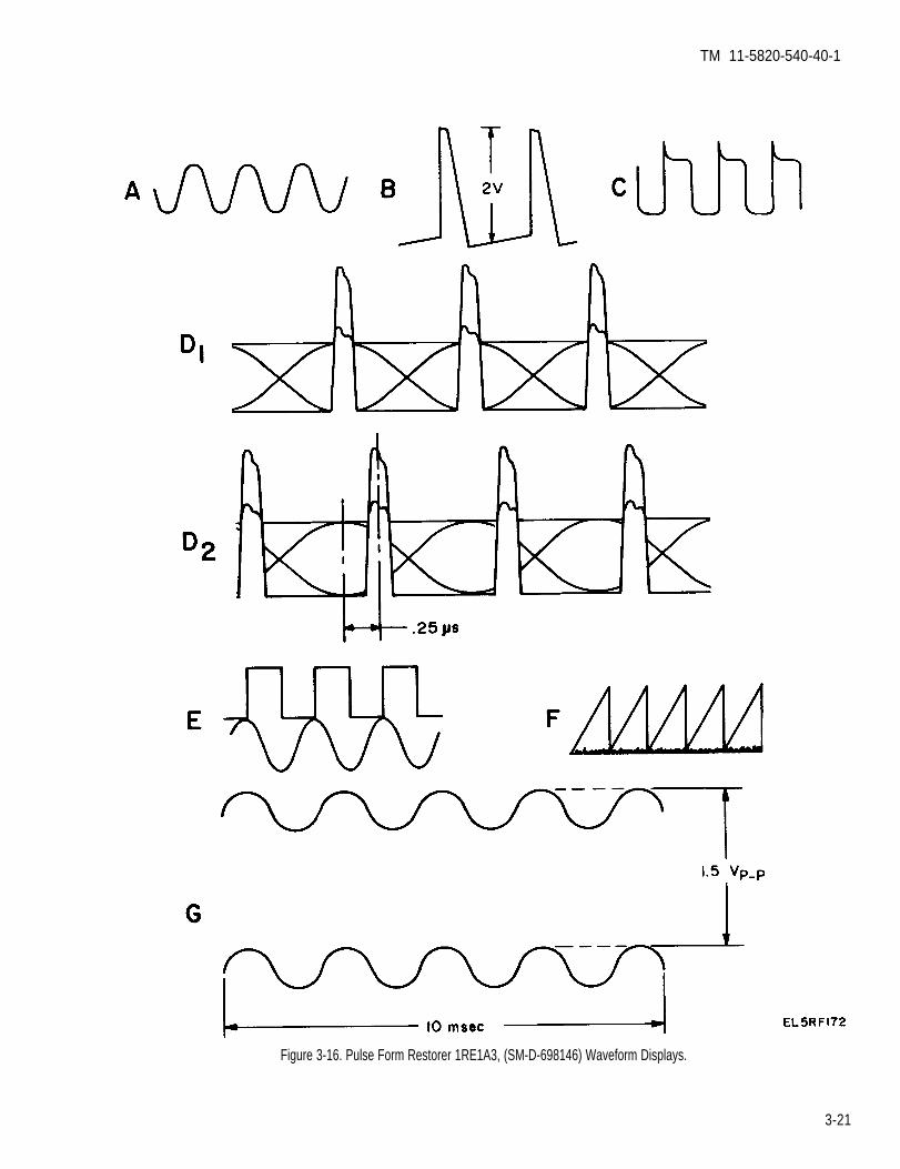
TM 11-5820-540-40-1
Figure 3-16. Pulse Form Restorer 1RE1A3, (SM-D-698146) Waveform Displays.
3-21
TM 11-5820-540-40-1
(c) Set the oscilloscope VERT MODE controlto ALT, the waveform displayed should be as shown inE, figure 3-16.
(d) Vary the test facility PCM LEVEL controlbetween 1.2 V and 1.75 V. The regenerated pcmamplitude and timing should remain constant (E, fig.3-16).
(e) Adjust the test facility PCM LEVEL controlto reduce the display (right channel) to 0.4 V peak-to-peak (E, fig. 3-16).
(f) Check to see that the regenerated pcmpulses displayed disappear and meter Ml indicateszero when the display for the right channel is reducedto 0.4 V peak-to-peak
(4) Order wire noise test(a) Connect the test equipment as shown in
figure 3-17.(b) Set switch S15 to the OUTPUT position.(c) Observe the oscilloscope left channel and
adjust the test facility PCM LEVEL control for a 1.5 Vpeak-to-peak display (G, fig. 3-16). The PCM LEVELmust remain at this setting for test (5) below. Note theVTVM indication it should be –16 dBm nominal. Thetest facility meter Ml should indicate in the greenband.
(d) Set switch S15 to NOISE: the VTVMshould indicate at least 32 dB below the indicationnoted in (c) above.
(5) Order wire gain and frequency response test.(a) Connect the test equipment as shown in
figure 3-18.(b) Set switch S15 to RESPONSE.(c) Set the coaxial switch to position 1. Adjust
the wide range osillator frequency to 1 kHz at an out-put level of 130 mvrs as indicated on the VTVM.
(d) Set the coaxial switch to position 2; theVRVM should indicate –9.5 dBm ±0.2 dB. Note theVTVM indication.
Symptom Probable cause
(e) Set S15 to OUTPUT. Meter Ml shouldindicate in the green band.
(f) Set S15 to RESPONSE. Set the coaxialswitch to position 1 and tune the wide range oscillatorto 200 Hz at an output level of 130 mvrms.
(g) Set the coaxial switch to position 2; theVTVM should indicate within ± 1 dB of the indicationnoted in (d) above.
(h) Repeat (f) and (g) above with the wide rangeoscillator tuned to 250 Hz, 500 Hz, 1.5 kHz, and 2 kHz.
(6) Order wire distortion test(a) Connect the test equipment as shown in A,
figure 3-19.(b) Rotate the test facilty PCM LEVEL control
fully ccw (minimum position).(c) Set switch S15 to DISTORTION.
(d) Tune the wide range oscillator frequency to1 kHz and adjust the output level to 365 mV peak-to-peak as indicated on the oscilloscope left channel.
(e) Vary the wide range oscillator frequencyadjustment slightly for a minimum indication on theVTVM. The level indicated on the VTVM should beless than –35 dBm.
(7) Order wire relay and combiner routing check.(a) Set test facility switch S15 to RESPONSE.(b) Connect the test equipment as shown in B,
figure 3-19. (The oscilloscope is not used in this test)(c) Tune the wide range oscillator frequency to
1 kHz and adjust the output level to obtain a –4 dBmindication on the VTVM.
(d) Connect the test equipment as shown in A,figure 3-19.
(e) Push and hold test facility switch S16 atTEST; the VTVM should indicate –10 dBm ±0.5 dB.
(f) Release S16 and set S15 to OFF.
C. Troubleshooting (FO-16).Ckecks and corrective measures
1. Sawtooth waveformleading edge blurredexcessively (b. (2)(e)above).
2. Timing pulse notpositioned at 0.25microsecond (b.(2)(g) above).
3. High noise level(b. (4)(d) above).
4. VTVM indication outof tolerance (b.(5)(d)above).
SLICER LEVEL control R13 on 1RE1A3A3 (fig. Adjust R13 as in d. (1) below.3-21) misadjusted.
PCM SYNC control R26 on 1RE1A3A3 (fig. 3-21) Adjust R26 as in d. (1) below.misadjusted
PCM CANCEL contol R11 and OW NOISE control Adjust R11 and R24 as in d. (2) below.R24 on 1RE1A3A1 (fig. 3-21) misadjusted.
OW GAIN control (R13 on 1RE1A3A1 (fig. 3-20) Adjust R13 as in d. (3) below.misadjusted
3-22

TM 11-5820-540-40-1
Figure 3-17. Pulse Form Restorer 1RE1A3, (SM-B6981 46) Order Wire Noise Check
3-23

TM 11-5820-540-40-1
Figure 3-18. Pulse Form Restorer 1RE1A3, (SM-D-698146) Order Wire Gain and Frequency Response Check Test Setup.
3-24

TM 11-5820-540-40-1
Figure 3-19. Pulse Form Restorer 1RE1A3, (SM-D-698146) Order Wire Distortion Check, Test Setup.
3-25

TM 11-5820-540-40-1
Figure 3-20. Modulation Eliminator 1RE1A3A1, Pulse Form Restorer 1RE1A3 (SM-D-698146) Parts Location.
3-26

TM 11-5820-540-40-1
Figure 3-21. Electrical Synchronizer 1RE1A3A3, Pulse Form Restorer 1RE1A3 (SMD-698146) Parts Location
NOTE
If the requirements of paragraph b. are notmet after performing the adjustments inparagraph d, replace the pulse form res-torer with Dual Rate Pulse Form RestorerSM-D-990510.
d. Adjustments.(1) PCM SYNC CONTROL R26 AND SLICER
LEVEL control R13 (1RE1A3A3).(a) Connect test equipment as shown in B,
figure 3-15.(b) Set test facility switch S1 to ON, and S15 to
OUTPUT.
(c) Adjust the PCM LEVEL control to obtain a1.5 V peak-to-peak display on the oscilloscope screenas shown in G, figure 3-16. Set test facility switch S15to NOISE.
(d) Connect the oscilloscope probe to the leftvertical INPUT of the oscilloscope and monitor TP1on 1RE1A3A3.
(e) Adjust SLICER LEVEL control R13(1RE1A3A3) for minimum blur (F, fig. 3-16). The saw-tooth amplitude will be constant (F, inset, fig. 3-16).
(f) Remove probe from TP1 and connect it toTIMING OUT, J46 on the test facility.
(g) Set oscilloscope to ADD.(h) Adjust vertical controls to obtain the
waveform shown in D1, figure 3-16.
3-27

TM 11-5820-540-40-1
Figure 3-22. Pulse Form Restorer 1RE1A3A2, Pulse Form Restorer 1RE1A3 (SM-D-698146) Parts Location
(i) Adjust R26 (1RE1A3A3) so that the timingpulse midpoints occur 250 nanoseconds to the right ofthe pcm pulse peaks (D2, figure 3-16).
NOTE
The center of the timing pulse must beexactly 250 nanoseconds to the right of thecenter of the pcm pulse peak
(j) Vary test facility FREQ ADJ control be-tween 575.975 kHz and 576.025 kHz while observingthe oscilloscope display. The relationship between thepcm pulses and the timing pulses shall remain cons-tant (synchronized) as shown in D2, figure 3-16.
3-28
(k) Reset FREQ ADJ control to 576.000 kHzas indicated on the frequency counter.
(2) PCM CANCEL control R11 and O W NOISEcontrol R24 (1RE1A3A1).
(a) Carry out (a) thru (c) of the order wire noisetest (b (4) above). Set S15 to NOISE.
(b) Adjust R11 PCM CANCEL and R24 OWNOISE control for a minimum indication on theVTVM.
(3) OW GAIN control R13 (1RE1A3A1).(a) Carry out (a) thru (d) of the order wire gain
and frequency response test (b. (5) above).(b) Adjust OW GAIN control R13 for a –9.5
dBm ±0.1 dB reading on the VTVM.

TM 11-5820-540-40-1
Figure 3-23. Pulse Form Restorer 1RE1A3 (SM-D-698146), Opened Showing Pulse Form Restorer 1RE1A3A2.
3-29

TM 11-5820-540-40-1
3-10. Dual Rate Pulse Form Restorer 1RE1A3(SM-D-990510), (Part No. CMC 245-8031 10-000)
a. Test Equipment and Material Required.
Equipment
Generator, Signal SG-1171/UTest Fixture, Restorer Pulse Form
TS-4116/GRM-95(V)2Oscilloscope AN/USM-281CFrequency Counter TD-1225(V)1/UGenerator, Signal AN/USM-205AVoltmeter, Electronic ME-459/UMultimeter AN/USM-451Test Facility, Transmitter
TS-28662/GRM-95(V)2Test Facility, Receiver
TS-28672/GRM-95(V)2Accessory Kit, Test Facilities Set
MK-1173(V)2/GRM-95(V)2
b. Test Procedure.
Common name
Signal generatorPFR test set
OscilloscopeFrequency counterWide range oscillatorVTVMMultimeterTransmitter test facility
Receiver test facility
Accessory kit
(1) Timing phase adjustments.(a) Connect test equipment as shown in A of
figure 3-24.(b) Install the pulse form restorer (PFR) unit
under test (UUT) onto connector J7 of the PFR testset and secure the mounting screw to the mountingblock.
(c) Set power supply PP-6304/GRM-95 to 115Vac as indicated on its panel voltmeter. Maintain thisindication throughout the following procedures.
(d) Set the PFR test set switches as follows:Switch Position
POWER ON/OFF (S7) ONPCM (S2) PR CODELEVEL SWITCH (S6) O dBFUNCTION (S1) 1COMBINER CONTROL (S5) 1kCOUNTER (S3) CLKVTVM (S4) VIDEONOISE (S8) OFFLOAD (S9) ON
(e) Adjust the PFR test set LEVEL ADJ con-trol (R12) for a level of 1.38 ±0.1 V peak-to-peak asindicated on right channel of the oscilloscope(triggered externally by SYNC signal). Do not disturbthe setting of the LEVEL ADJ control (R12) for theremainder of these tests.
(f) Adjust the FREQ CONTROL (R5) on thePFR test set for 576.000 Hz ±1 Hz as indicated on thefrequency counter. Set the FUNCTION switch (S1) toposition 2.
(g) Set the PFR test set PCM switch (S2) toposition 10.
(h) Connect test equipment as shown in Bfigure 3-24. Monitor both the DCDR CLK and theDCDR PCM of the UUT, on oscilloscope LEFT andRIGHT channels respectively (use J 11 and J13 onPFR test set as common points). Adjust the oscillo-scope TRIGGER control to obtain waveforms asshown in figure 3-25.
(i) Adjust the PHASE ADJ potentiometer ofthe unit under test such that pulse widths T1 and T2shown in figure 3-25 are equal.
(2) Timing output test.(a) Connect the equipment as shown in figure
3-26.(b) Set the PFR test set switches as follows:
Switch Position
FUNCTION (S1) 1COMBINER CONTROL (S5) OPENPCM (S2) PR CODELOAD (S9) ON
(c) Observe the TIMING OUTPUT waveformon LEFT channel of the oscilloscope. Ensure it is syn-chronized with the SYNC signal. The TIMING OUT-PUT pulse should have the following characteristics:
1. A level of 1.8 Vp-p to 2.2 Vp-p, measuredfrom the average baseline to the peak. Ignore a smallpip, if present
2. Rise and fall times (10% to 90%amplitude) of 25 nsec to 45 nsec.
3. Pulse width at 50% points, of 85 nsec to145 nsec.
(d) On the PFR test set set the PCM switch(S2) to OFF for 5 seconds, then return it to the PRCODE position.
(e) The TIMING OUTPUT waveform shouldremain synchronized with the VIDEO waveform dis-played on oscilloscope LEFT and RIGHT channelsrespectively.
(f) Set the PFR test set LEVEL SWITCH (S6)to the –6 dB, O dB, and +6 dB positions. The TIM-ING OUTPUT and VIDEO waveforms should remainsynchronized.
(g) Set the PFR test set LEVEL SWITCH (S6)tn O dB.
(h) Adjust the PFR test set FREQ CONTROL(R5) for a clock frequency of 576,090 Hz ±2 Hz asindicated on the frequency counter. Repeat steps (d)through (g) above.
(i) Adjust the PFR test set FREQ CONTROL(R5) for a clock frequency of 575,910 Hz ±2 Hz asindicated on the frequency counter. Repeat steps (d)through (g) above.
3-30
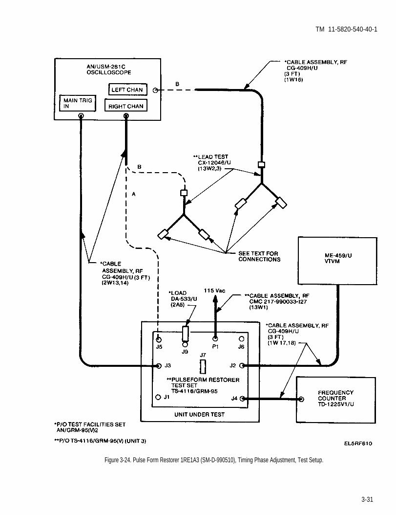
TM 11-5820-540-40-1
Figure 3-24. Pulse Form Restorer 1RE1A3 (SM-D-990510), Timing Phase Adjustment, Test Setup.
3-31

TM 11-5820-540-40-1
Figure 3-25. Pulse Form Restorer 1RE1A3 (SM-D-990510), Waveform Diagram of DCDR PCM and DCDR CLK
(j) Set the PFR test set switches as follows (3) PCM output check
Switch Position
FUNCTION (S1) 3COMBINER CONTROL (S5) 1k
(k) Adjust the PFR test set FREQ CONTROL(R5 for a clock frequency of 1,152,000 Hz ±2 Hz asindicated on the frequency counter. Repeat steps (d)through (g) above.
(l) Adjust the PFR test set FREQ CONTROL(R5) for a clock frequency of 1,152,180 Hz ±2 Hz as 3-27.
(a) Set the PFR test set switches as follows
Switch Position
FUNCTION (S1) 1COMBINER CONTROL (S5) OPENPCM (S2) 10 CODELEVEL SWITCH (S6) 0 dBLOAD (S9) OFF
(b) Connect test equipment as shown in figureAdjust the PFR test set FREQ CONTROL (R5)
indicated on the frequency counter. Repeat steps (d) for a clock frequency of 576,000 Hz ±2 Hz asthrough (g) above. indicated on the frequency counter.
(m) Adjust the PFR test set FREQ CONTROL (c) Set the oscilloscope LEFT CHAN and(R5) for a clock frequency of 1,151,820 Hz ±2 Hz as RIGHT CHAN inputs to DC. Observe the PCMindicated on the frequency counter. Repeat steps (d) waveform and the TIMING OUTPUT waveform onthrough (g) above. oscilloscope LEFT and RIGHT channels respectively.
3-32

TM 11-5820-540-40-1
Figure 3-26. Pulse Form Restorer 1RE1A3 (SM-D-99051O), Timing Output, Test Setup.
3-33

TM 11-5820-540-40-1
Figure 3-27. Pulse Form Restorer 1RE1A3 (SM-D-9905 10), Pcm Output Test Setup.
3-34

TM 11-5820-540-40-1
(d) The PCM pulse should have the followingcharacteristics:
1. Logic “1” level: 0.0 V to –0.2 V.2. Logic “0” level: –1.8 V to –2.2 V.3. Rise and fall times (10% to 90%
amplitude): 10 ns to 45 ns.4. Delay of rising pcm pulse transitions re-
lative to 50% point of rising edge of timing output: 40ns to 75 ns.
(e) Set the PFR test set switches as follows:
Switch Position
FUNCTION (S1) 3COMBINER CONTROL (S5) 1kPCM(S2) 10 CODELEVEL SWITCH (S6) +6 dB
(f) Repeat steps(c) and(d) above.(g) Set PCM (S2) to PR CODE and LEVEL
SWTICH (S6) to 0 dB.(h) Remove the 91 ohm load at the oscilloscope
channel. Both the PCM and the TIMING OUTPUTsignals should disappear. The signals should reappearwhen the 91 ohm load is replaced.
(i) Set the PFR test set PCM switch (S2) toOFF. Both the PCM and the TIMING OUTPUTsignals should disappear.
(j) Set the PCM switch (S2) back to the PRCODE position The signals should reappear.
(k) Using the multimeter, measure the voltagesat J10 (+) and J11 (—) of the PFR test set The mul-timeter should indicate between 230 and 280 mV.
(4) Order wire check(a) Set the PFR test set switches as follows:
Switch position
FUNCTION (S1)VTVM (S4)PCM (S2)COMBINER CONTROL (S5)COUNTER (S3)NOISE (S6)LOAD (S9)LEVEL SWITCH (S6)
4VIDEOOFFOPENOW FREQOFFOFF0 dB
(b) Adjust the wide range oscillator for a fre-quency of 1000 Hz ±2 Hz and a level of –16 dBm±0.1 dB as indicated on the counter and the VTVMrespectively.
(c) Set the PFR test set switches as follows:
Switch Position
VTVM (S4) OW NOISEPCM (S2) PR CODE
(d) Adjust the LF ADJ potentiometer on theunit under test and fine tune the 1 kHz signal fre-quency of the test oscillator for a minimum indicationon the VTVM (typically below —40 dBm). Adjust theOW NOISE potentiometer on the UUT and then read-just the LF ADJ on the UUT for a minimum indicationon the VTVM. Record the indication.
(e) Set the PFR test set VTVM switch (S4) toOW LEVEL. The VTVM should indicate –10 dBm±0.5 dB. Record this indication.
(f) Set the PFR test set COMBINER CON-TROL switch (S5) to GND. The VTVM should indi-cate –16 dBm ±0.5 dB.
(g) Reset the COMBINER CONTROL switch(S5) to OPEN. Set the test oscillator to sweep between250 Hz and 2 kHz as read on the frequency counter.The VTVM reading should not vary by more than ±0.4dB from the indication recorded in (e) above.
(h) Tune the wide range oscillator frequency to1000 Hz ±2 Hz.
(i) Set the PFR test set VTVM switch (S4) toOW NOISE. Fine tune the test oscillator frequency fora minimum indication on the VTVM (typically below–40 dBm).
(j) Set the PFR test set LEVEL SWITCH (S6)as listed below. The VTVM should indicate less thanthe maximum indications listed below.
LEVEL SWITCH (S6) position Maximum indication
6 dB –30 dBm0 dB –40 dBm
-6 dB –42 dBm
(k) If the reading at –6 dB is below –44 dBmreadjust the OW NOISE control on the unit under testuntil the reading is –42 dBm, then repeat step (j)above.
(l) Set the PFR test set switches as follows:
Switch Position
FUNCTION (S1) 5COMBINER CONTROL (S5) 1 k
(m) Set the PFR test set LEVEL SWITCH(S6) as listed below. The VTVM should indicate lessthan the maximum indication listed below.
LEVEL SWITCH position Maximum indication
6 dB –33.0 dBmO dB –39.0 dBm
-6 dB –45.0 dBm
(n) Reset the PFR test set LEVEL SWITCH(S6) to 0 dB.
3-35

TM 11-5820-540-40-1
(o) Using the digital multirneter, measure theOW voltage between J12(+) and J13(–). The mul-timeter should indicate between 230 and 280 mV.
(5) 576 kb/s error rate check
NOTE
In order to count the error pulses generatedover the required time interval, it will benecessary to use an external time base forthe frequency counter, and to calibrate theoscilloscope to trigger at a vertical inputlevel of –10 mV.
(a) Set the PFR test set switches as follows:
Switch Position
FUNCTION (S1) 1VTVM (S4) VIDEOCOUNTER (S3) ERRORSPCM (S2) OFFCOMBINER CONTROL (S5) OPENNOISE (S8) ONLOAD (S9) ON
(b) vary the NOISE ADJ control (R11) on thePFR test set for an indication of 0.103 vrms on theVTVM. (Set VTVM volts scale to 1 volt after settingnoise level.)
(c) Set the PFR test set PCM switch (S2) to PRCODE.
(d) Refer to figure 3-28. Using the frequencycounter and VTVM, adjust the signal generator fre-quency to 1 MHz ±1 kHz at an output level of 2 volts.
(e) Connect test equipment as shown in figure3-28.
(f) Position INT-EXT OSC switch (rear of fre-quency counter) to EXT OSC and RESOLUTIONswitch (front panel) to 1 Hz. The frequency counter isnow set for a sample time of 10 seconds.
(g) Set the oscilloscope switches as follows:Switch Position
VERT MODETRIG SOURCEAC-GND-DC (left chennel)VOLTS/DIV (left channel)MAIN TRIGGERING MODEMAIN TRIGGERING COUPLINGMAIN TRIGGERING SOURCEMAIN TRIGGERING SLOPEMAIN TRIGGERING LEVELTIME/DIV
LEFTLEFTGND10 mVAUTODCINTNEG(–)CENTER50 us
(h) Position the trace (left channel) to theupper half of the graticule. Set MAIN TRIGGERINGMODE to NORM
3-36
(i) Repeatedly adjust the left channel POSI-TION control to move the trace towards the bottomhalf of the graticule while adjusting the MAINTRIGGERING LEVEL control until triggering justoccurs at the center vertical graticule line.
(j) Set MAIN TRIGGERING MODE to AUTO.Adjust the left channel POSITION control to place thetrace 1 cm above the center vertical graticule line.
(k) Set the MAIN TRIGGERING MODE toNORM and left channel AC-GND-DC switch to AC.The oscilloscope is now calibrated to trigger on allnegative going pulses of—10 mV or greater.
(l) The frequncy counter reading should notexceed 58 errors in the 10 second interval establishedin (f) above.
(6) 1152 kb/s error rate check.(a) Set the PFR test set switches as follows:
Switch Position
COUNTER (S3) ERRORSPCM (S2) OFFFUNCTION (S1) 3COMBINER CONTROL (S5) 1kNOISE (S8) ONVTVM (S4) VIDEOLOAD (S9) ON
(b) Vary the NOISE ADJ control (R11) on the PFR test set for an indication of 0.062 vrms on theVTVM. Set VTVM VOLTS scale to 1 volt after settingnoise level.
(c) Set the PFR test set PCM switch (S2) to PRCODE. The frequency counter should count less than115 errors in a 10 second interval.
(d) Set the PFR test set switches as follows:
Switch Position
PCM (S2) OFFCOUNTER (S3) OW FREQNOISE (S8) OFFFUNCTION (S1) 5COMBINER CONTROL (S5) 1kLOAD (S9) ON
(e) The VTVM should indicate –16 dBm ±0.1dB. If necessary, adjust wide range oscillator level con-trol to obtain this reading.
(f) Temporarily position INT-EXT OSC switch(rear of frequency counter) to INT. Refer to figure 3-28. Using the frequency counter and VTVM: adjustthe signal generator for and output frequency of166.667 Hz ±200 Hz at a level of 2 volts. Adjust theoutput frequency of the wide range oscillator to 1000Hz ±2 Hz.

TM 11-5820-540-40-1
Figure 3-28. Pulse Form Restorer 1RE1A3, Error Rate Check Test Setup.
3-37

TM 11-5820-540-40-1
Figure 3-29. Pulse Form Restorer 1RE1A3 (SM-B990510), Pin Diagrams, Integrated Circuits.
(g) Reposition INT-EXT OSC switch to EXT.Connect equipment as shown in figure 3-28. Fre-quency counter is now set for a sample time of 60seconds.
(h). Set the PFR test set switches as follows:Switch Position
PCM (S2) PR CODECOUNTER (S3) ERRORSNOISE (S8) OFFFUNCTION (S1) 5COMBINER CONTROL (S5) 1kLOAD (S9) ON
(i) The frequency counter should count lessthan 100 errors in a 60-second interval.
C. Troubleshooting (FO-17).(1) In order to troubleshoot the pulse form res-
torer it is necessary to gain access to the interior cir-cuitry. See paragraph 3-10 d. for disassembly andassembly instructions.
(2) To troubleshoot Pulse Form Restorer1RE1A3, connector test equipment as shown in figure3-27 (S9 OFF). Figures 3-29 and 3-30 show the loca-tion of pins on the integrated circuits and transistors.Figures 3-31, 3-32, 3-33, and 3-34 show the postion ofcomponents and test points on each board.
(3) Refer to the table below to determine themost probable location of faults.
Output signal abnormal Most likely location of fault
PCM, PCM meter Board A2Timing pulses Board A4Order wire, order wire meter Board A1Order wire relay Board A3
(4) After determining probable location of faulttroubleshoot as described in the appropriate chartbelow.
3-38

TM 11-5820-540-40-1
Figure 3-30. Pulse Form Restorer 1RE1A3 (SM-D-990510), Pin Diagram Transistor.
Figure 3-31. Pulse Form Restorer 1RE1A3 (SM-D-990510), Pulse Form Restorer Pcb 1RE1A3A2, Component Location Diagram.
3-39

TM 11-5820-540-40-1
Figure 3-32. Pulse Form Restorer 1RE1A3 (SM-D-990510), Modulation Eliminator Pcb 1RE1A3A1, Compment Location Diagram
c. Troubleshooting. - ContinuedSymptom Checks and corrective measures
PULSE FORM RESTORER BOARD 1RE1A3A2
No pcm pulse Check that there are no broken wires on 1RE1A3A2. Check that the +5 V, +12 V and –12 V supply voltages appear atindication E4, ES, and E7 respectively (fig. 3-31). If the voltage levels are incorrect check ground connection at E5 and E6 for
broken wires. If the +12 V or –12 Vie absent, check the wires attached to E8 and E7. If the +5 V is abesnt check thewire at E4. If it is not broken, measure the voltage at pin 2 of the external regulator. It should be +5 V. The voltage atpin 1 should be +12 V.
Pcm waveform a To check board 1RE1A3A2 (fig. 3-31) in the binary mode, follow b. through y. below. Set the PFR test set switches asabnormal indicated below and use the SYNC signal from the test set to trigger the scopce:(binarymode).
Switch
FREQ CONTROL (R5)LEVEL SWITCH (S6)FuNCTION (S1)NOISE (S6)PCM (S2)COMBINER CONTROL (S5)LOAD (S9)
Position
Center of range0 dB1OFFPR CODEOPENOFF
3-40

TM 11-5820-540-40-1
Figure 3-33. Pulse Form Restorer 1RE1A3 (SM-D-990510), Electrcial Interface Pcb 1RE1A3A3, Component Location Diagram.
c. Troubleshooting. – Continued
Symptom Checks and corrective measures
PULSE FORM RESTORER BOARD 1RE1A3A2 - (Cont)
Pcm waveform b.abnormal(binary c.mode)- (Cont) d.
e.
f.
g.
h.
i
j.
k
l.
Check that the input signal at E3 is as shown in figure 3-35 (1a). If incorrect check the PFR test set
If the signal at pin 6 of U13 is not as shown m figure 3-35 (3a), replace U13.
If the signal at E2 is not as shown in figure 3-35 (3a), replace Q1.
If the signal at pin 6 of U12 is not as shown in figure 3-35 (3a), replace U12.
Check that the signal at pin 7 of U8 switches between 0 V and greater than 4.5 V. If it does not change U8.
The signal at pin 3 of U5 should be 0.75 Vdc ±0.1 V. If it is not replace Q2.
Check that the signal at pin 1 of US is 0.75 Vdc ±0.1 V. If it is not replace U5.
The signal at pin 7 of U7 should switch between O V and greater than 4.5 Vdc. If it does not change U7.
Check that the signal at the collector of Q3 is 0.75 Vdc ±0.1 V. If it is not, change Q3.
Check that the signal at pin 7 of U5 is -0.75 Vdc ±0.1 V. If it is not then change U5.
The signal at pin 14 of U5 should be 1.5 Vdc ±0.2 V. If it is not replace U5.
3-41
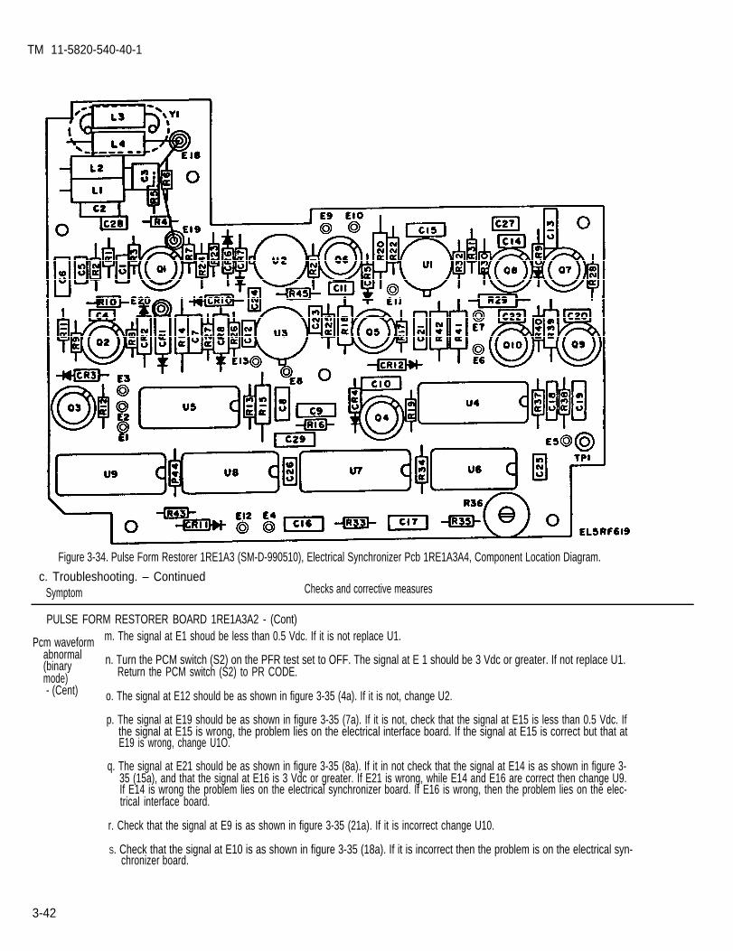
TM 11-5820-540-40-1
Figure 3-34. Pulse Form Restorer 1RE1A3 (SM-D-990510), Electrical Synchronizer Pcb 1RE1A3A4, Component Location Diagram.
c. Troubleshooting. – ContinuedSymptom Checks and corrective measures
PULSE FORM RESTORER BOARD 1RE1A3A2 - (Cont)
Pcm waveform m. The signal at E1 shoud be less than 0.5 Vdc. If it is not replace U1.abnormal(binary n. Turn the PCM switch (S2) on the PFR test set to OFF. The signal at E 1 should be 3 Vdc or greater. If not replace U1.
Return the PCM switch (S2) to PR CODE.mode)- (Cent) o. The signal at E12 should be as shown in figure 3-35 (4a). If it is not, change U2.
p. The signal at E19 should be as shown in figure 3-35 (7a). If it is not, check that the signal at E15 is less than 0.5 Vdc. Ifthe signal at E15 is wrong, the problem lies on the electrical interface board. If the signal at E15 is correct but that atE19 is wrong, change U1O.
q. The signal at E21 should be as shown in figure 3-35 (8a). If it in not check that the signal at E14 is as shown in figure 3-35 (15a), and that the signal at E16 is 3 Vdc or greater. If E21 is wrong, while E14 and E16 are correct then change U9.If E14 is wrong the problem lies on the electrical synchronizer board. If E16 is wrong, then the problem lies on the elec-trical interface board.
r. Check that the signal at E9 is as shown in figure 3-35 (21a). If it is incorrect change U10.
S. Check that the signal at E10 is as shown in figure 3-35 (18a). If it is incorrect then the problem is on the electrical syn-chronizer board.
3-42

TM 11-5820-540-40-1
Figure 3-35. Waveform Diagrams for Pulse Form Restorer 1RE1A3 (SM-D-990510) (Sheet 1 of 8).
3-43
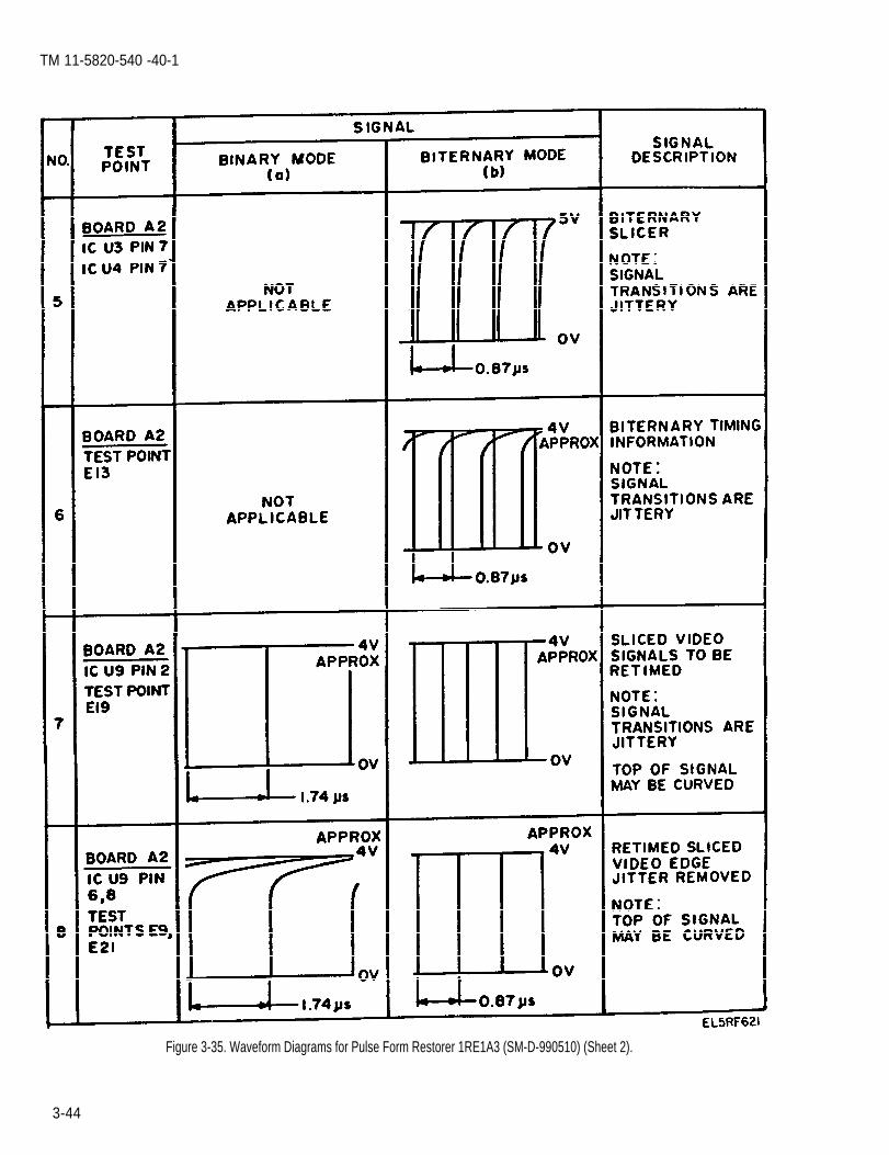
TM 11-5820-540 -40-1
Figure 3-35. Waveform Diagrams for Pulse Form Restorer 1RE1A3 (SM-D-990510) (Sheet 2).
3-44

TM 11-5820-540-40-1
Figure 3-35. Waveform Diagrams for Pulse Form Restorer 1RE1A3 (SM-D-990510) (Sheet 3).
3-45
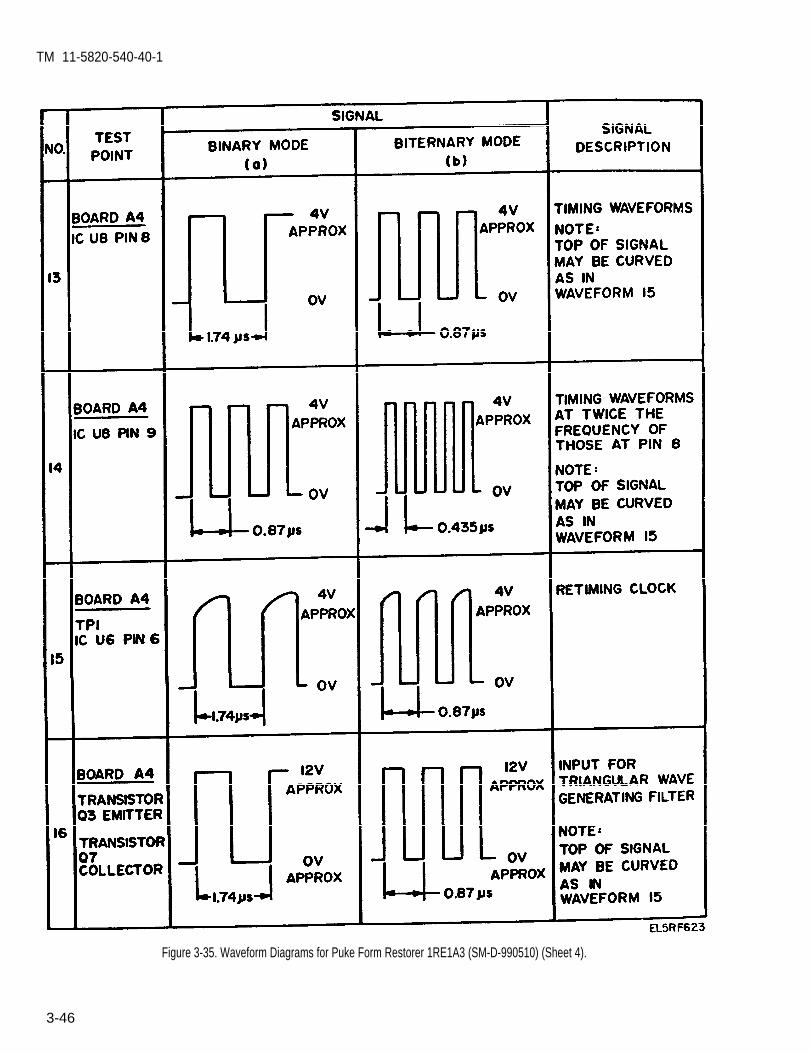
TM 11-5820-540-40-1
Figure 3-35. Waveform Diagrams for Puke Form Restorer 1RE1A3 (SM-D-990510) (Sheet 4).
3-46

TM 11-5820-540-40-1
Figure 3-35. Waveform Diagrams for Pulse Form Restorer 1RE1A3 (SM-D-990510) (Sheet 5).
3-47

TM 11-5820-540-40-1
Figure 3-35. Waveform Diagrams for Pulse From Restorer 1RE1A3 (SM-LM90510) (Sheet 6).
3-48
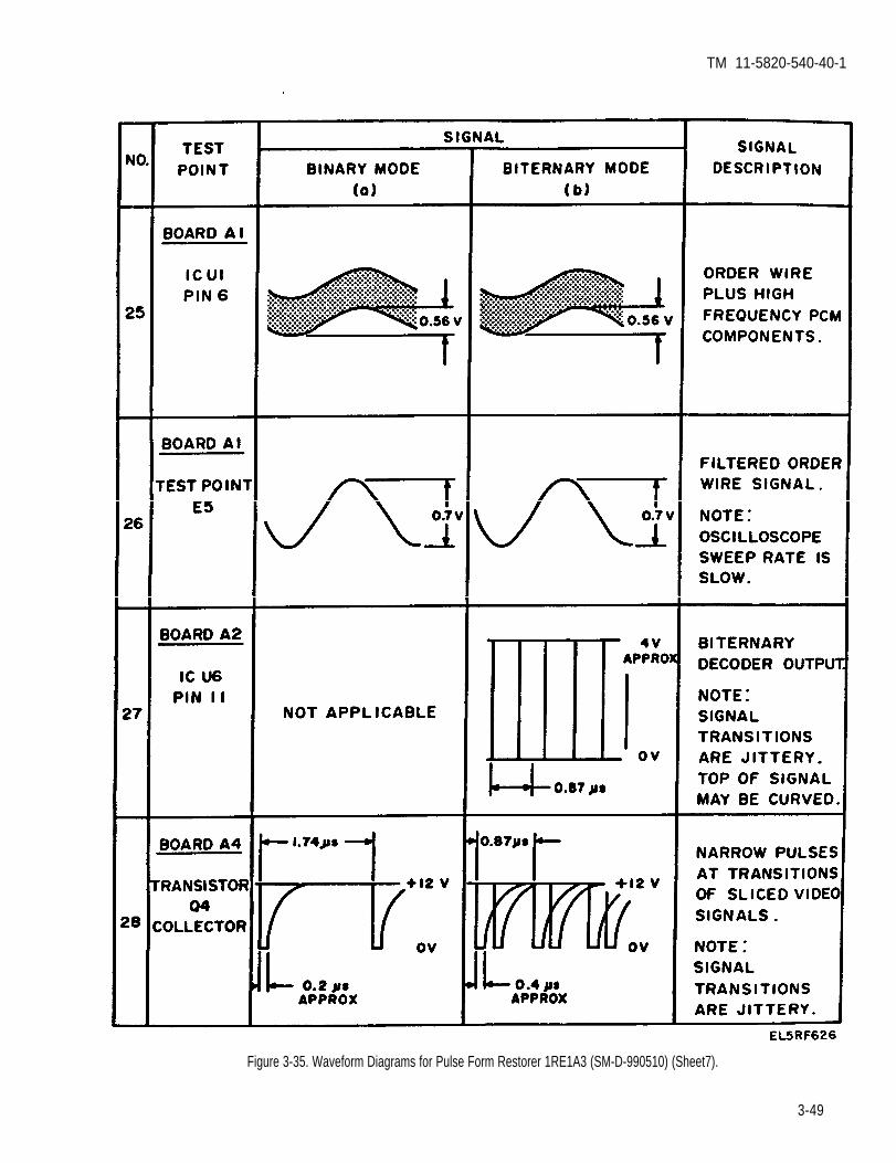
TM 11-5820-540-40-1
Figure 3-35. Waveform Diagrams for Pulse Form Restorer 1RE1A3 (SM-D-990510) (Sheet7).
3-49

TM 11-5820-540-40-1
Figure 3-35. Waveform Diagram for Pulse Form Restorer 1RE1A3 (SM-D-990510) (Sheet 8).
3-50

TM 11-5820-540-40-1
c. Troubleshooting. – Continued
Symptom Checks and corrective measures
PULSE FORM RESTORER BOARD 1RE1A3A2 - (Cont)
Pcm waveformabnormal(binarymode)- (Cent)
Pcm waveformabnormal(biternarymode)
t.
u.
v.
w.
x.
y.
a.
Check that the signal at pin 3 of U11 is as shown in figure 3-35 (21a). If it is not, change U11.
Check that the signal at E11 is as shown in figure 3-35 (21a). If it is not change U11.
The signal at E20 should be as shown in figure 3-35 (21a). If it is not, then the problem is on the electrical synchronizerboard.
The signal at the emitter of Q4 should be switching between –0.5 and +4 Vdc ±.0.5 V. If it is not, change Q4
The signal at E18 should be as shown in figure 3-35 (9a). If it is not then change Q5.
The signal at E17 should be between 0.2 Vdc and 0.3 Vdc. If not, check the following components and replace ifnecessary CR3, CR4, C11, C23, R49 and R50.
To check board 1RE1A3A2 (figure 3-31) in the biternary mode, follow b. through v. below. Set the PFR test set switchesas indicated below
FREQ CONTROL (R5) Center of rangeLEVEL SWITCH (S6) O dBFUNCTION (S1) 3NOISE (S8) OFFPCM (S2) PR CODECOMBINER CONTROL 1k OHM
b. The signal at E15 should be 3 Vdc or greater. If it is not then there is a fault on the electrical interface board.
c. Check that the signal at pin 6 of U13 is as shown in figure 3-35 (3b). If it is incorrect replace U13.
d Check that the signal at E2 is as shown in figure 3-35 (3b). If it is incorrect, change Q1.
e. Check that the signal at pin 6 of U12 is as shown in figure 3-35 (3b). Change U12 if the signal is wrong.
f. The signal at pin 7 of U8 should switch between O V and greater than 4.5 Vdc. If it does not replace U8.
g. Check that the signal at pin 3 of U5 is 1.2 Vdc ±0.1 V. If it is not, replace Q2.
h. The signal at pin 1 of U5 should be 1.2 Vdc ±0.1 V. If it is not replace U5.
i. The signal at pin 7 of U7 should switch between O V and greater than 4.5 Vdc. If it does not change U7.
j. Check that the signal at the collector of Q3 is 1.2 Vdc ±0.1 V. If it is not, change Q3.
k. Check that the signal at pin 7 of U5 is –1.2 Vdc ±0.1 V. If it is not replace U5.
l. The signal at pin 7 of U3 should be as shown in figure 3-35 (5b). If it is incorrect, change U3.
m. The signal at pin 7 of U4 should be as shown in figure 3-35 (5b). If it is incorrect change U4.
n. The signal at E13 should be as shown in figure 3-35 (6b). If it is incorrect change U6.
o. Check that the signal at pin 11 of U6 is as shown in figure 3-35 (27 b). If it is incorrect change U6.
p. The signal at E19 should be as shown in figure 3-35 (7 b). If it is not, then check if the signal at E15 is greater than 3Vdc. If E15 is incorrect the problem is on the electrical interface board. If E15 is correct, and E19 is wrong, then changeU10.
3-51

TM 11-5820-540-40-1
c. Troubleshooting. – Continued
symptom Checks and corrective measures
PULSE FORM RESTORER BOARD 1RE1A3A2 - (Cont)
Pcm waveform q.abnormal(biternarymode)- (Cont)
r.
s.
t.
u
v.
The signal at pin 8 of U9 should be as shown in figure 3-35 (8 b). If it is not check that the signal at E14 is as shown infigure 3-35 (15b) and that the signal at E16 is 3 Vdc or greater. If the signal at U9, pin 8 is wrong while E14 and E16are correct, change U9. If E 14 is wrong, the problem is on the electrical synchronizer board If Ex6 is wrong, the problemis on the electrical interface board.
Check that the signal at E9 is as shown in figure 3-35 (8 b). If incorrect change U10.
Check that the signal at E10 is as shown in figure 3-35 (18 b). If it is incorrect the problem is on the electrical syn-chroniser board.
Check that the signal at pm 13 of U11 is as shown in figure 3-35 (8b). If it is not, replace U11.
Check that the signal at E11 is as shown in figure 3-35 (8b). If it is incorrect, replace U10.
Check that the signal at E22 is M shown in figure 3-35 (8b). If it is incorrect, change U10.
ELECTRICAL SYNCHRONIZER BOARD 1RE1A3A4
No timing Check that there are no broken wires on 1RE1A3A4. Check that the +5 V, +12 V and –12 V supply voltages appear atpulse E8, E9 and E10 respectively (figure 3-34). If voltage levels are incorrect, check ground connection at E11 for a brokenindication. wire. If the +12 V or –12 V supplies are absent check the wiring attached to E9 and E10. If the +5 V is absent check
the wire attached to E4. If the wire is not broken check the external regulator U5. The voltage at pin 2 should be 5 V.The voltage at pin 1 should be 12 V.
Timing output a.waveformabnormal(binarymode).
b.board.
c.
d
e.
f.
g.
h.
i
To check board 1RE1A3A4 (figure 3-34) m the binary mode, follow b. through z. below. Set the PFR teat set switches asindicated below:
Switch Position
FREQ CONTROL (R5) Center of rangeFUNCTION (S1) 1NOISE (S6) OFFLEVEL SWITCH (S6) 0 dBPCM (S2) PR CODECOMBINER CONTROL (S5) OPENLOAD (S9) OFF
The signal at E12 should be as shown in figure 3-35 (8a). If it ix incorrect then the problem is on the pulse form restorer
The signal at E13 should be as shown in figure 3-35 (7a). If it is incorrect change U5.
The signal at E6 should be 3 Vdc or greater. If it is incorrect there is a fault on the electrical interface board.
Check that the signal at E3 is less than 0.5 Vdc. If it is not, there is a fault on the electrical interface board.
The signal at E4 should be as shown in figure 3-35 (18a). If it is incorrect, check that the signal at the collector of Q2contains an oscillatory component greater than 1.8 V peak-to-peak If the output of Q2 is correct while E4 is wrong,change Q3. If there is no oscillation at the collector Q2, check the bias voltages on U1. The base should be at 2.7 Vdc,the emitter at 2.0 Vdc, while the collector should be at 2.7 Vdc. If the bias voltages differ from these values by more than0.2 V, one ore more of the bias resistors, R1, R2, R4, R5, R6 or transistor Q1 may be faulty. If these components arefound to be working correctly, check Q2.
The signal at E2 should be as shown in figure 3-35 (4a). If not there is a fault on the pulse form restorer board.
The signal at pin 1 of U5 should be as shown in figue 3-35 (10a). If it is incorrect, change U9.
The signal at pin 11 of U5 should be as shown in figure 3-35 (11a). If it is incorrect replace U5.
3-52

TM 11-5820-540-40-1
c. Troubleshooting. – Continued
Symptom Checks and corrective measures
ELECTRICAL SYNCHRONIZER BOARD 1RE1A3A4 - (Cont)
Timing outputwaveformabnormal(binarymode) -(Cent)
Timing outputwaveformabnormal(biternarymode).
j. The signal at the collector of Q4 should be as hewn in figure 3-35 (28a). If it is incorrect, then replace Q4.
k. The signal at the collector of Q5 should be as shown in figure 3-35 (12a). If it is wrong change Q5. If it is still wrongafter changing Q5, then replace Q6.
l. The signal at pin 8 of U8 should be as shown in figure 3-35 (13a). If it is incorrect, replace U8.
m The signal at pin 9 of U8 should be as shown in figure 3-35 (14a). If it is incorrect, change U8.
n.
o.
P.
q.
r.
s.
t.
u
v.
w.
x.
y.
z.
a.
The signal at pin 12 of U7 should be as shown in figure 3-35 (29a). If it is not, replace U7.
The signal at pin 4 of U7 should be as shown in figure 3-35 (30a). The pulse width should be adjustable over the givenrange by potentiometer R36. If the signal is incorrect change U7. If the adjustment does not function, change R36.
The signal at TP1 should be as shown in figure 3-35 (15a). If it is incorrect replace U6.NOTE: this signal should be synchronized with the SYNC signal from the PFR test set.
If the signal at pin 6 of U6 is not as shown in figure 3-35 (15a), then replace U6.
The signal at the collector of Q7 should be as shown in figure 3-35 (16a). If it is incorrect replace Q7.
The signal at the emitter of Q8 should be as shown in figure 3-35 (16a). If it is incorrect, replace Q8.
If the signal at pin 6 of U1 is not a triangular waveform as shown in figure 3-35 (17a), then replace U1.
The signal at pin 3 of U2 is a dc voltage of leas than 0.5 Vdc when the signal at TP1 is synchronized with the SYNCsignal from the PFR test set. If it is incorrect change Q6.
The signal at pin 6 of U2 should be less than 0.5 Vdc when TP1 signal is synchronized with the SYNC signal. If it is not,change U2.
The signal at pin 6 of U3 is a variable dc voltage which depends on the difference between the input bit rate and the cen-ter frequency of the voltage controlled oscillator. It can vary between –0.5 V and +10 V. Normally it should be approx-imately +5 V. If it goes below —0.5 V, then change CR10. If it goes above +10 V, then change CR8. If the voltage is stillnot correct replace U3.
The signal at pin 4 of U4 should appear as in figure 3-35 (19a). If it is incorrect, replace U4.
The signal at the collector of Q9 should appear as shown in figure 3-35 (31a). If it is incorrect, then replace Q9.
The signal at E7 should be as shown in figure 3-35 (20a). If it is incorrect change Q10.
To check board 1RE1A3A4 (figure 3-34) in the binternary mode, follow b. through t below. Set the PFR test setswitches as indicated below.
Switch Position
FREQ CONTROL (R5) Center of rangeLEVEL SWITCH (S6) O dBFUNCTION (S1) 3PCM (S2) PR CODECOMBINER CONTROL (S5) 1 K OHMNOISE (S8) OFFLOAD (S9) OFF
b. The signal at E3 should be 3 Vdc or greater. If the level is incorrect, there is a fault on the electrical interface board:
c. The signal at E 1 should be as shown in figure 3-35 (6 b). If it is incorrect there is a fault on the pulse form restorerboard.
3-53

TM 11-5820-540-40-1
c. Troubleshooting. – Continued
Symptom Checks and measures
ELECTRICAL SYNCHRONIZER BOARD 1RE1A3A4 - (Cont)
Timing output dwaveformabnormal e.(biternarymode) - f.(Cent)
g.
h.
i.
j.
k.
l.
m.
n.
o.
p.
q.
r.
s.
t.
The signal at pin 1 of U5 should be as shown in figure 3-35 (10b). If it is incorrect replace U9.
If the signal at pin 11 of U5 is not as shown in figure 3-35 (11b), change U5.
IF the signal at the collector of Q4 is not as shown in figure 3-35 (28b), change Q4.
The signal at the collector of Q5 should be as shown in figure 3-35 (12b). If incorrect change Q5. If incorrect aftercahnging Q5, then change Q6.
If the signal at pin 8 of U8 is not as shown in figure 3-35 (13b), then change U8.
If the signal at pin 9 of U8 is not as shown in figure 3-35 (14b), then change U8.
If the signal at pin 12 of U7 is not as shown in figure 3-35 (29b), then change U7.
The signal at pin 4 of U7 should be as shown in figure 3-35 (30b). The pulse width should be adjustable over the givenrange by potentiometer R36. If the signal is incorrect, then change U7. If the signal cannot be adjusted, then changeR36.
The signal at TP1 should be as shown in figure 3-35 (15b). If it is incorrect then replace U6.NOTE: this signal should be synchronized with the SYNC signal from the PFR test set.
If the signal at pin 6 of U6 is not as shown in figure 3-35 (15b), then replace U6.
If the signal at the collector of Q7 is not as shown in figure 3-35 (16b), then replace Q7.
If the signal at the emitter of Q8 is not as shown in figure 3-35 (16b), then replace Q8.
The signal at pin 6 of U1 should be triangular waveform as shown in figure 3-35 (17b). If it is not, then replace U1.
The signal at pin 3 of U2 is a dc voltage of less than 0.5 Vdc when the signal at TP1 is synchronized with the SYNCsignal from the PFR test set If it is incorrect then change Q6.
The signal at pin 6 of U2 should be less than 0.5 Vdc when the TP1 signal is synchronized with the SYNC signal If it isnot, then change U2.
The signal at pin 6 of U3 is a variable de voltage which depends on the difference between the input bit rate and the cen-ter frequency of the voltage controlled oscillator. It can very between -0.5 V end +10 V. Normally it should be approx-imately +5 V. If it goes below –0.5 V, change CR10. If it goes above +10 V, change CRE. If after changing CR8 andCR10 the voltage is still not correct then replace U3.
Turn the PCM switch (S2) on the PFR test set to OFF. Check that the signal at E6 is less than 0.5 Vdc. If it is not there
Order wiresignalabnormal(binarymode).
is a fault either on the pulse form restorer board, or on the electrical interface board. If E6 is correct then the signal atE7 should go to zero. If it does not change U4.
MODULATION ELIMINATOR BOARD 1RE1A3A1
No order wire Check that there are no broken wires on 1RE1A3A1. Check that the +5 V, +12 V, –12 V supply voltages appear at E4,output. E6, end E8 respectively (figure 3-32). If the voltage levels are incorrect check the ground connection at E7 for a broken
wire. If the +12 V or – 12 V is absent, check the wiring attached to E6 and E8. If the +5 V is absent check the wiringattached to E4. If the wires are not broken then check the external regulator U5. The voltage at pin 2 should be 5 V. Thevoltage at pin 1 should be 12 V.
a. To check 1RE1A3A1 (figure 3-32) in the binary mode, follow b. through n. below. Set the PFR test set switches asindicated below and use the SYNC signal from the teat set to trigger the scope:
3-54
TM 11-5820-540-40-1
c. Troubleshooting. – Continued
Symptom Checks and corrective measures
MODULATION ELIMINATOR BOARD 1RE1A3A1 - (Cont)
Order wire a.signalabnormal(biternarymode) -(Cent)
b.
c.
d
e.
f.
g.
h.
i.
j.
k.
L
Continued Switch Position
FREQ CONTROL (R5) Center of rangeLEVEL SWITCH (S6) 0 dBFUNCTION (S1) 4NOISE (S8) OFFPCM (S2) PR CODECOMBINER CONTROL (S5) OPENLOAD (S9) OFF
Check that the signal at E3 is as shown in figure 3-35 (2 la). If it is not correct then there is a fault on the pulse form res-torer board.
Check that the signal at E2 is as shown in figure 3-35 (22a). If it is incorrect there is a fault on the pulse form restorerboard.
Check that the signal at El 1 appears as shown in figure 3-35 (23a). If it is not correct then there is a fault on the pulseform restorer board.
The signal at El should appear as shown in figure 3-35 (2a). If the signal is incorrect then there is a fault on the pulseform restorer board.
If the signal shape at the collector of Q1 is not as shown in figure 3-35 (32a), then replace Q1.
The signal shape at the collector of Q2 is as shown in figure 3-35 (32a).NOTE: the amplitude is different from the signal at the collector of Q1. If the signal shape is wrong, replace Q2. If thesignal is wrong at both the collectors of Q1 and Q2, then check Q3 and CR3.
The shape of the signal at pin 6 of U3 should be as shown in figure 3-35 (24a). If the shape is wrong, change U3.NOTE: the amplitude may be different if another part of the board is not functioning properly.
The signal at pin 6 of U1 should be as shown in figure 3-35 (25a). If the signal is incorrect replace U1.
The signal at pins 6 and 9 of U2 should be a voltage of 1.8 Vdc ±0.1 V. If it is incorrect change U2.
The signal at pin 14 of U4 should be a voltage of less than 0.5 Vdc. If not, change U4.
The signal at pin 1 of U4 should be a voltage of –7.4 Vdc to –8.0 Vdc. If it is incorrect replace U4.
m. The signal at E5 should be a faltered sine wave as shown in figure 3-35 (26a). If it is not correct change U4.
n.
Order wire a.signalabnormal(biternarymode).
b.
The signal at E9 should be a dc voltage between 2.7 Vdc and 4.0 Vdc. If the level is incorrect check CR1, CR2, andC30, as well as C11 and R14 on the electrical interface board.
To check board 1RE1A3A1 (figure 3-32) in the biternary mode, follow b. through n. below. Set the PFR test set switchesas indicated below:
Switch Position
FREQ CONTROL (R5) Center of rangeLEVEL SWITCH (S6) O dBFUNCTION (S1) 5NOISE (S8) OFFPCM (S2) PR CODECOMBINER CONTROL (S5) 1 KOHMLOAD (S9) OFF
Check that the signal at E3 is as shown in figure 3-35 (21b). If it is incorrect, there is a fault on the pulse form restorerboard.
3-55

TM 11-5820-540-40-1
c. Troubleshooting. - Continued
Symptom Checks and corrective measures
MODULATION ELIMINATOR BOARD 1RE1A3A1 - (Cont)
c.
d.
e.
f.
g.
h.
i.
j.
k.
l.
The signal at E2 shoudl be as shown in figure 3-35 (22b). If it is incorrect there is a fault on the pulse form restorerboard
If the signal at E11 is not as shown in figure 3-35 (23b), or if the signal at E1 is not as shown in figure 3-35 (2b), thenthere is a fault on the pulse form restorer board
The signal shape at the collector of Q1 should be as shown in figuer 3-35 (32b). If the signal shape is wrong, replace Q1.
The signal shape at the collector of Q2 is as shown in figure 3-36 (32b).NOTE: the amplitude is difference from the signal at the collector of Q. If the signal shape is wrong, replace Q2. If thesignal is incorrect at both Q1 and Q2, then check Q8 and CR3.
The signal shape at pin 6 of U3 should be as shown in figure 3-35 (24b). If the shape is wrong change U3.NOTE the amplitude may be different if another part of the board is not functioning properly.
The signal at pin 6 of U1 should be as shown in figure 3-36 (25b). If the signal is incorrect, change U1.
The signal at pins 6 and 9 of U2 should be a voltage of 1.8 Vdc ±0.1 V. If incorrect, then change U2.
The signal at pin 14 U4 should a voltage of less than 0.5 Vdc. If it is not, change U4.
The signal at pin 1 of U4 should be a voltage of –5.6 Vdc to -6.2 Vdc. If it is incorrect, change U4.
If the signal at E5 is not a filtered sine wave as shown in figure 3-35 (26b), then change U4.
m The signal at E9 should be a voltage between 2.7 V and 4.0 V. If it is incorrect check CR1, CR20 and C30; check as wellC11 and R14 on the electrical interface board
n. If all the signals are correct but the order wire baa a high amount of noise then check potentiometer R23 and R29.
ELECTRICAL INTERFACE BOARD 1RE1A3A3
Order wire arelayoperationdefective.
b.
c.
d
e.
Check that there are no broken wires on 1RE1A3A3. Check that the +5 V, +12 V and –12 V supply voltages appear atE2, E4 and E5 respectively (figure 3-33). If the voltage levels are incorrect, check the ground correction at E3 forbroken wires. If the +12 V or –12 Via absent check the wiring attached to E5 and E4. If the +5 Via absent, check thewiring at E2. If the wire is not broken, measure the voltage at pin 2 of the external regulator U5. It should be +5 V. Thevoltage at pin 1 should be 12 V.
To check operation of 1RE1A3A3, set the PFR test set switches to the positions indicated below and perform steps c.through u. following.
Switch Position
FREQ CONTROL (R5) Center of rangeLEVEL SWITCH (S6) O dBFUNCTION (S1) 4NOISE (S8) OFFPCM (S2) PR CODECOMBINER CONTROL (S5) OPENLOAD (S9) OFF
The signal at E6 should be 2.7 Vdc to 4.0 Vdc. If incorrect there could be a fault on the pulse form restorer board, or afault in R14 or C11.
The signal at E7 should be 0.2 Vdc to 0.3 Vdc. If incorrect check R14 and C11.
The signal at E14 should be approximately 0 Vdc. If it is incorrect there is a fault on the pulse form restorer board
3-56

TM 11-5820-540-40-1
c. Troubleshooting. – ContinuedSymptom Checks and corrective measures
ELECTRICAL INTERFACE BOARD 1RE1A3A3 - (Cont)
Order wire f.relayoperationdefective g.
- (Cent)h.
i.
j.
k.
L
The signal at E12 should be as shown in figure 3-35 (9a). If it is incorrect there is a fault on the pulse form restorerboard.
The signal at the collector of Q1 should be between–5 Vdc and –7 Vdc. If it is not, check Q1 and CR1.
The signal at the collector of Q2 should be greater than 3 Vdc. If it is not, check Q2, CR2, C9 and U1.
The signal at pin 13 of U1 should be less than 0.5 Vdc. If it is not, then change U1.
The signal at E15 should be greater than 3 Vdc. If it is not, then change U1.
Set PFR test set LOAD switch (S9) to the OFF position. The signal at E12 should be –12 Vdc ±0.5 V. If it is not, and ifEl 5 is less than 0.5 Vdc, then there is a fault on the pulse form restorer board. (U9 on that board is the most likely causeof the problem.) If the signal at E15 is greater than 3 Vdc, then the fault is on the electrical interface board.
The signal at the collector of Q2 should be less than 0.5 Vdc. If it is not, check Q1, Q2, CR1 and CR2.
m. The signal at pin 13 of U 1 should be greater then 3 Vdc. If it is not, replace U1.
n.
o.
p.
q.
r.
8.
t.
u.
Set the PFR test set LOAD switch (S9) to the ON position.
The signal at the E15 should be less than 0.5 Vdc. If not change U1.
Set the PCM switch (S2) on the PFR test set to the OFF position. The signal at E14 should be greater than 3 Vdc. If itis not, there is a fault on the pulse form restorer board.
Set the PCM switch (S2) on the PFR test set to PR CODE. The signal at pin 7 of U3 should be a dc voltage greater than3 Vdc. If it is not change U3. The signal at pin 7 of U2 should be less than 0.5 Vdc. If not, change U2. The collector ofQ3 should be 26 Vdc. If not change Q3. The signal at E10 should be as shown in figure 3-35 (26a). If it is not changethe relay K1. The signal at E13 should be less than 0.5 Vdc. If not, change U1.
Set the COMBINER CONTROL switch (S5) on the PFR test set to 1 k The signal at pin 7 of U3 should be less than0.5 Vdc. If it is not, then change U3. The signal at pin 7 of U2 should be less then 0.5 Vdc. It is not then change U2. Thesignal at E13 should be greater than 3 Vdc. If it is not, then replace U1. The collector of Q3 should be at 26 Vdc. If it isnot, then change Q3. The signal at E10 should be as shown in figure 3-35 (26 b). If it is not, then replace relay K1.
Set the COMBINER CONTROL switch (S5) on the PFR test set to GND. The signal at pin 7 of U3 should be less than0.5 Vdc. If not change U3. The signal at pin 7 of U2 should be greater than 1.5 Vdc. If not, replace U2. The signal atE13 should be less than 0.5 Vdc. If not replace U1. The signal at the collector of Q3 should be less than 0.5 Vdc. If it isnot, then replace Q3.
The signal at E11 should be a sine wave with a peak-to-peak voltage of about 0.7 Vdc. If it is not then check the PFRtest set
The signal at E10 should be a sinewave with a peak-to-peak voltage of about 0.35 Vdc, If it is not then replace relay K1.
d. Disassembly and Assembly. NOTE
(1) Removal and disassembly. This unit need not be disassembled for test-ing. All test points are accessible with the
(a) Remove Pulse Form Restorer 1RE1A3 covers of the unit in place. Should itfrom Radio Receiver 1RE1 as described in TM 11- become necessary to replace a component5820-540-12. however, the covers of the unit must be
(b) To gain access to the four circuit boards removed to provide access to the interiorperform steps (c) through (f) below. circuitry.
3-57

TM 11-5820-540-40-1
(c) For boards 1RE1A3A1 and 1RE1A3A2(the modulation eliminator and pulse form restorerboards respectively) locate the side of the unit whichbears the DCDR PCM, OW NOISE, and LF ADJ testpoints. Remove the 4 corner screws which secure thebrass cover in place and liftoff the cover.
(d) Board 1RE1A3A1 now faces outward. Togain access to board 1RE1A3A2, remove the fivescrews securing board 1RE1A3A1 to the unit’s case.Genetly lift out board 1RE1A3A1, being careful not tostrain the wires which attach it to the other boards.The bottom of board 1RE1A3A2 is now visible.Access to the top of board 1RE1A3A2 can be obtainedby lifting the board up by its top edge while being care-ful not to place undue strain on the wires which secureit to the other boards.
(e) For boards 1RE1A3A4 and 1RE1A3A3(the electrical synchronizer and electrical interfaceboards respectively) locate the side of the unit whichbears the DCDR CLK and PHASE ADJ test points.Remove the 3 corner screws which secure the brasscover in place and liftoff the cover.
(f) Board 1RE1A3A4 now faces outward. Togain access to board 1RE1A3A3, remove the sixscrews securing board 1RE1A3A4 to the unit’s case.Gently lift out board 1RE1A3A4 being careful not tostrain the wires which attach it to the other boards.The bottom of board 1RE1A3A3 is now visible.Access to the top of board 1RE1A3A3 can be obtainedby lifting the board up by its top edge while being care-ful not to place undue strain on the wires which secureit to the other boards.
(2) Assembly. To reassemble the unit, place thecircuit boards back inside the case. They should lieflat. Be certain that no wires are caught under thescrew holes in the boards. Securely fasten each set oftwo boards with the five slotted-head screws andreplace the covers. Secure the covers with the appropriate number of screws (four screws for the coverbearing the OW NOISE, LF ADJ and DCDR PCMtest points; three screws for the other cover).
3-11. Electrical Frequency Limiter-Discriminator 1RE1A4
a. Test Equipment and Material Required.
Equipment
Test Facility, ReceiverTS-2867(V)2/GRM-95(V)2
Test Facility, TransmitterTS-2866(V)2/GRM-95(V)2
Accessory Kit, Test Facilities SetMK-1173(V)2/GRM-95(V)2
Multimeter, Digital,AN/USM-451
Common name
Receiver test facility
Transmitter test facility
Accessory kit
Digital Multimeter
Equipment Common name
Generator, Signal, Wide range oscillatorAN/USM-205A
Frequency Counter, Frequency counterTD-1225(V)1/U
Voltmeter, Electronic, ME-459/U VTVMGenerator, Signal, HP 8640B Signal generatorMeter, Modulation, ME-505/U Deviation meterOscilloscope, AN/USM-281C oscilloscope
b. Performance Test(1) AGC line continuity.
(a) Connect the digital multimeter between P1pins 1 and 4, and then between P1 pin 1 and P2 pin 1.The digital multimeter shall read less than 0.5 ohms.
(b) Connect the digital multimeter between P1and 1 and ground. The digital multimeter shall indicateand open.
(2) Output level.(a) Set the power supply to 115 Vac as
indicated on its front panel voltmeter. Maintain thislevel throughout the remaining procedures.
(b) Connect the equipment as shown in A,figure 3-36.
(c) Set test facility switches as follows:Switch Position
AT1 70S1 ONS5 S9S14 30 MHzS9 EXT VIDEO
(d) Set the wide range oscillator to 1 kHz out-put and adjust the level for a VTVM indication of 178mV.
(e) Connect equipment as shown in B, figure 3-36. The VTVM shall indicate 178 ±5 mV.
(3) Discriminator linearity.(a) Install oscilloscope right vertical amplifier
plug in unit into the horizontal amplifier position of theoscilloscope and the horizontal amplifler into the rightvertical amplifier position.
(b) Connect test equipment as shown in A,figure 3-37. Set S9 to DISCR RESPONSE.
(c) Set the oscilloscope controls to display a S-shaped curve as shown in figure 3-38.
(d) Adjust the signal generator output level andtest facility AT1 as necessary to display a 30 MHzmarker on the S-shaped curve (see figure 3-38).
(e) The waveform displayed on the oscilloscopeshould be an S-shaped curve with frequency peak-to-peak excursion, linearity and amplitude between peaksas shown in figure 3-38.
(f) connect test equipment as shown in B, figure 3-37.
3-58

TM 11-5820-540-40-1
Figure 3-36 Electrical Frequency Limiter-Discrirninator 1RE1A4, Output Level Check, Test Setup.
(g) Set test facility switch S9 to EXT VIDEO.(h) Set the wide range oscillator frequency to
50 kHz and adjust its output level for 100 kHz devia-tion as measured on the deviation meter. Note andrecord the VTVM indication.
(i) Repeat step (h) above with test facilityswitch S14 set to 29 and 31 MHz in turn.
(j) Calculate the maximum difference betweenVTVM indications obtained m steps (h) and@ above.The difference should not exceed 10% of the maximumindication recorded.
(4) Frequency response.(a) Connect the test equipment as shown in
figure 3-39.
(b) Set S9 to EXT VIDEO and S14 to 30 MHz.(c) Set the wide range oscillator to 10 kHz.
Adjust the 0-10 dB attenuator and wide rangeoscillator amplitude control as required to establish a–60 dBm reference indication on the VTVM with awide range oscillator panel meter indication in theupper 10% F.S.D (meter scale NORMAL).
(d) Set the wide range oscillator to EXPANDmeter scale and adjust the reference control to centerscale. This meter indication is the input amplitude.Reference at all test frequencies.
(e) Set the wide range oscillator to 125 Hz andadjust the amplitude control to maintain the referenceinput level in (d) above. The VTVM shall be within±1.5 dB of reference established in (c) above.
3-59

TM 11-5820-540-40-1
Figure 3-37. Electrical Frequency Limiter-Discriminator 1RE1A4, Discriminator Linearity Check, Test Setup.
3-60

TM 11-5820-540-40-1
Figure 3-38. Electrical Frequency Limiter-Discrimina tor 1RE1A4, S-Shape Curve Oscilloscope Display.
(f) Repeat (e) above for all other frequencieslisted below.
Wide Range OscillatorFreq kHz VTVM Level
0.20.51.0
10.0100.0200.0500.0800.0900.0960.0
1000.0
Reference ±1.5 dBReference ±1.5 dBReference ±1.0 dBReferenceReference ±0.3 dBReference ±0.6 dBReference ±0.8 dBReference ±0.8 dBReference ±0.8 dBReference ±0.8 dBReference ±0.8 dB
C. Troubleshooting (FO-18).
(1) Initial Checks.(a) Dc supply check. Check the –12 Vdc at E5
(AR1), E1 (A4), and E1 (A3).(b) Preliminary capacitor setup. If capacitor
assembly A5 is replaced while troubleshooting, carryout the following preliminary adjustments beforerepeating the alignment procedure given in d. below.
1. Turn C1, C2, and C3 clockwise to theirstops.
2. Turn C1 5 turns counterclockwise.3. Turn C2 2 turns counterclockwise.4. Turn C3 9 turns counterclockwise.5. Center R1.
(2) Troubleshooting chart
NOTE
The p-p voltages in the chart are typical indications measured with the allocated oscilloscope.
Symptom Probable cause Checks and corrective measures
(a) No output indication (b.(2)(b) above). 1. Defective electrical noise limiter. Set test facility switch S9 to 30 MHz.Observe input signal at E2 of A3 (1.25 Vp-p) and output signal at E5 (1.5 Vp-p). If out-put signal is abnormal, replace A3.
3-61

TM 11-5820-540-40-1
Figure 3-39. Electrical Frequency Limiter-Discriminator 1RE1A4, Frequency Response Check, Test Setup.
3-62

TM 11-5820-540-40-1
Troubleshooting - ContinuedSymptom Probable cause Checks and corrective measures
2. Defective electrical noise limiter A4.
3. Defective video amplifier AR1.
4. Defective discriminator subassembly A1or C1 of A5.
(b) Upper half of S-shaped DISCR RE- 1. Defective A1-diode CR1 shorting or TP1SPONSE curve missing. (b.(3)(d) open circuitabove).
2. Defective capacitor C3 (A5).
(c) Lower half of S-shaped DISCR RE- 1. Defective A1-diode CR2 shorting or TP1SPONSE curve missing (b.(3)(d) above). open circuit
2. Defective capacitor C2 (A5).
(d) Difference between VTVM indications Misalined or defective capacitor assemblyexceeds 10% (b.(3)(i) above). (A5).
(e) Frequency response abnormal (b.(4)(e) Defective discriminator 1RE1A4,above).
Check the output signal at E5 of A4 (1.0 Vp-p). If abnormal, replace A4.
Check signal at E3 (400 mVp-p). If normal,check resitance between E3 and the centerpin of 1RE1A4P2A1 (0 to 2 k ohms) replaceR2 if indicated Check signal at E2 (1.375Vp-p) and E4 (2.125 Vp-p). If normalreplace AR1.
Check the signal at E3 of A1 (approx. 1.25Vp-p). If indication is abnormal disconnectand check C1 and C4 of A5. Replace ifnecessary. If C1 and C4 are normal, replaceA1. Check voltage at E6 (1.375 Vp-p)nominal and E7 (2.125 Vpp) of A1. ReplaceA1 if indications are abnormal. Recheckvoltage at E6 and E7 of A1. If still abnor-mal replace A5.
1. Check resistance of diode CR1 (acrossE6 and ground) and continuity of T1 (E5to ground).
2. Check C3 for short short circuit.
1. Check resistance of CR2 (across E7 andground) and continuity of T1 (E4 toground).
2. Check C2 for short circuit
Aline discriminator 1RE1A4 as in d. below.If necessary, replace capcitor assembly A5and realine 1RE1A4.
Repeat the checks in b.(2) above at theabnormal frequency and perform thetroubleshooting checks in paragraph (c.(2)(a)above). Replace subassemblies as indicated.
d. Alinement Procedures.(1) Remove the unit under test cover plates and
install test covers C W-1083/GRM-95 (V) (2MP2) andDWG A307435 (3A38).
(2) Connect test equipment as shown in A, figure3-40 and set test facility switches as follows:
Switch Position
AT1 70S1 ONS5 S9S14 30 MHzS9 DISCR RESPONSE
(3) Set the oscilloscope HORIZ and VERT con-trols to obtain a display similar to the display shown infigure 3-41.
(4) The CHAN B (right channel) waveform dis-played on the oscilloscope should be an S-shapedcurve with frequency peak to peak excursion andlinearity similar to the CHAN A (left channel) S-shaped curve. The amplitude between peaks should be3 ±1 volt P-P (figure 3-41). If necessary adjust R2, C1,C2 and C3 to meet above requirements.
(5) Connect test equipment as shown in B, figure3-40.
(6) Adjust signal generator output level and testfacility AT1 as necessary to display a 30 MHz markeron the CHAN B (right oscilloscope channel) S-shapedcurve.
(7) Adjust the signal generator frequency asnecessary to determine the frequency peak-to-peakexcursion of the CHAN B (right oscilloscope channel)S-shaped curve. It should be 4 ±1 MHz (figure 3-41).
3-63

TM 11-5820-540-40-1
Figure 3-40. Electrical Frequency Limiter-Discriminator 1RE1A4, Alinement Test Setup.
(8) Connect test equipment as shown in C, figure3-40.
(9) Adjust the signal generator for an output levelof –30 dBm at 30 MHz with 50% amplitude modula-tion. Adjust R1 for a minimum oscilloscope right chan-nel (CHAN B) indication. NOTE: Normal” indication isless than 1 millivolt P-P.
(10) Reconnect test equipment as shown in A,figure 3-40.
(11) Adjust the oscilloscope vertical sensitivityand position controls to align the CHAN A and CHANB S-shaped curve slopes parallel with each other.Adjust C1, C2 and C3 for best slope match betweenCHAN A and CHAN B S-shaped curves (figure 3-41).
(12) Repeat steps (8) thru (11) until no furtheradjust is necessary.
(13) Connect test equipment as shown in C, figure3-36.
3-64

TM 11-5820-540-40-1
Figure 3-41. Electrical Frequency Limiter-Discriminator 1RE1A4, Channel A and B Waveform Display.
(14) Set tst facility switch S9 to EXT VIDEO. SetAT1 to minimum output required to operate deviationmeter.
(15) Set the wide range oscillator frequency to 50kHz and adjust its output level for 100 kHz deviationas measured on the deviation meter. Note and recordthe VTVM indication.
(16) Repeat step (15) above with test facilityswitch S14 set to 29 and 31 MHz in turn.
(17) Calculate the maximum difference betweenVTVM indications obtained in steps (15) and (16)above. The difference should not exceed 10% of themaximum indication recorded.
NOTE
If above requirement is not met, slight read-justment of C1, C2 or C3 maybe necessaryto minimize the difference. If any adjust-ment is necessary recheck R1 adjustmentper step (8) and (9) above.
(18) Connect test equipment as shown in B, figure3-36.
(19) Set test facility switch S14 to 30 MHz. Setwide range oscillator frequency to 1 kHz and adjust itsoutput level for 500 kHz deviation as measured on thedeviation meter and set AT1 to 70. The VTVM shouldindicate 178 ±10 mV. If necessary adjust R2 for aVTVM indication of 178 mV.
(20) Repeat test in paragraph b(2) through (4)above.
3-12. Amplifier Frequency Multipliera. Test Equipment Required
Equipment
Test Facility, TransmitterTS-2866(V)2/GRM-95(V)2
Accessory Kit, Test FacilitiesMK-1173(V)2/GRM-95(V)2
Test Facility, ReceiverTS-2867(V)2/GRM-95(V)2
Sweep Generator, Wiltron 61ODPlug-in Unit Wiltron 61084D
Power Meter HP-435APower Sensor HP-8481AOscilloscope AN/USM-281CRf Power AmplifierENI 6031Signal Generator HP-8640BRf Voltmeter ME-426/UDigital Multimeter AN/USM-451
Common name
Transmitter test facility
Accessory kit
Receiver test facility
Sweep generator
Power meterPower sensorOscilloscopePower amplifierSignal generatorRf voltmeterDigital multimeter
NOTE
Set power supply PP-6304/GRM-95(V) fora 115 Vac output as indicated on its panelvoltmeter. Maintain this output through outthe following procedures.
3-65
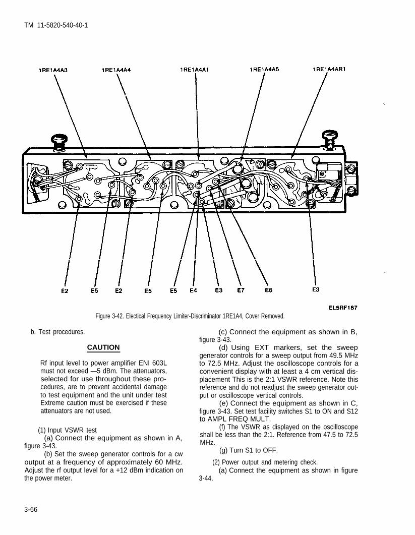
TM 11-5820-540-40-1
Figure 3-42. Electical Frequency Limiter-Discriminator 1RE1A4, Cover Removed.
b. Test procedures.
CAUTION
Rf input level to power amplifier ENI 603Lmust not exceed —5 dBm. The attenuators,selected for use throughout these pro-cedures, are to prevent accidental damageto test equipment and the unit under testExtreme caution must be exercised if theseattenuators are not used.
(1) Input VSWR test(a) Connect the equipment as shown in A,
figure 3-43.(b) Set the sweep generator controls for a cw
output at a frequency of approximately 60 MHz.Adjust the rf output level for a +12 dBm indication onthe power meter.
(c) Connect the equipment as shown in B,figure 3-43.
(d) Using EXT markers, set the sweepgenerator controls for a sweep output from 49.5 MHzto 72.5 MHz. Adjust the oscilloscope controls for aconvenient display with at least a 4 cm vertical dis-placement This is the 2:1 VSWR reference. Note thisreference and do not readjust the sweep generator out-put or oscilloscope vertical controls.
(e) Connect the equipment as shown in C,figure 3-43. Set test facility switches S1 to ON and S12to AMPL FREQ MULT.
(f) The VSWR as displayed on the oscilloscopeshall be less than the 2:1. Reference from 47.5 to 72.5MHz.
(g) Turn S1 to OFF.
(2) Power output and metering check.(a) Connect the equipment as shown in figure
3-44.
3-66

TM 11-5820-540-40-1
Figure 3-43. Ampl#ier-Frequency Multiplier 1RE1A5, VSWR, Test Setup.
3-67

TM 11-5820-540-40-1
Figure 3-44. Amplifier-Frequency Multiplier 1RE1A5, Power Output and Metering, Test Setup.
(b) Set test factility switches S1 to ON and S12to AMPL FREQ MULT.
(c) Set the signal generator for an output levelof +14 dBm at 47.5 MHz.
(d) Slowly increase the signal generator fre-quency to 72.5 MHz while observing the power meterindication. The power meter should indicate +4 dBm,+3.0-0 dB.
(e) Repeat (c) and (d) above observing the digi-tal multimeter. The digital multimeter should read be-tween 175 and 350 mVdc.
(3) Harmonic and fundamental frequency rejectiontest
(a) Connect the equipment as shown in figure3-45 using the 95 to 190 MHz filter, and set testfacility switch S1 to ON.
(b) Set the signal generator to 47.5 MHz andadjust the OUTPUT LEVEL control for an output of+12.5 dBm.
(c) Adjust the filter around 142.5 MHz for apeak indication on the rf voltmeter. This is the thirdharmonic of the UUT input frequency. The peak rfvoltmeter indication should not exceed —16 dBm.
3-68

TM 11-5820-540-40-1
Figure 3-45. Amplifier-Frequency Multiplier 1RE1A5, Harmonic Rejection Test Setup.
(d) Tune the signal generator from 47.5 to 72.5MHz while maintaining a peak indication on the rfvoltmeter by tracking the filter to the third harmonic ofthe signal generator frequency (142.5 to 217.5 MHzfilter frequency). The rf voltmeter peak indicationshould not exceed –16 dBm.
NOTE
For third harmonic frequencies above 190MHz (63.3 MHz signal generator fre-quency), change to the 190 to 400 MHzfilter.
(e) set the signal generator to 48.5 MHz andtune the 190 to 400 MHz falter around 194 MHz for apeak rf voltmeter indication of the fourth harmonic.The rf voltmeter shall not indicate more than –16 dB.
(f) Repeat (b) through (d) above using the 48 to95 MHz filter tuned to the fundamental (input) fre-quencies from 48.3 to 72.5 MHz. The rf voltmeterpeak indication shall not exceed –16 dBm.
(g) Set the signal generator to 60 MHz.(h) Tune the 48 to 95 MHz filter for a peak
indication on the rf voltmeter. The indication shall notbe greater than –36 dBm.
(i) Set receiver test facility switches S1 andS12 to OFF.
3-69

TM 11-5820-540-40-1
c. Troubleshooting Procedure (FO-19).Remove the four countersunk screws securing the top cover and the six screws securing the bottom cover of1RE1A5.
Amplifier-Frequency Multiplier 1RE1A5, Troubleshooting Chart
symptom Proboble cause Checks and corrective measures
(1) VSWR display exceeds 2:1 reference (a) Miaalinement of 1RE1A5.(b.(l)(f).
(b) Defective lowpass filter 1RE1A5FL1(fig. 3-46).
(c) Defective resistors R1 or R2, trans-former T1, or rectifier pair CR1 figure3-46.
(2) No output (b.(2)(d)).
(3) Output normal, DMM readingOut of tolerance (b(2)(e)).
(4) Abnormal output level (b.(2)(d).
(d) Defective transistor Q1 or related circuit
(a) No dc supply to transistor stages.
(b) Defective circuit components or wiring.
Defective components in meter circuit
(a) 1RE1A5 alinement incorrect.
(a) If VSWR display is less than the 2:1reference for most of the display, aline1RE1A5 as described in e. below(adjustment of R1, R2, C5 and C11 canaffect input VSWR).
(b) Using oscilloscope, check the inputsignal at E1 and E3 (1RE1A5FL1) withthe sweep generator in manual sweepmode, the signal should be the sameamplitude at both points. Check for con-tinuity between El and E3(1RE1A5FL1). Check component,replace 1RE1A5FL1, if defective.
(c) Using the oscilloscope check the signalwaveform and amplitude at the base ofQ1 (para. d. below). A difference inamplitude between adjacent peaksindicates defective components or mis-adjustment of R1 or R2.
(d) Check Q1 and related circuit. Replacedefective components.
(a) Check +12 V and –12 V supply to tran-sisator stages.
(b) (1) Using the oscilloscope, check theinput signal at E1 and E3(1RE1A5FLI) as indicated m dbelow. If signal is not present at E3,check the continuity of L1 thru LA(1RE1A5FL1) (figure 3-46). Checkconnector and cable A1 to E1(1RE1A5FL). Replace if defective.
(2) Check signal through transistor stages(d below) and observe doubler lctionIf signal at Q1 is abnormal, check con-tinuity of transformer T1 windingsand forward and reverse resistance ofdiode CR1.
(3) Check continuity of components fromQ3 and E4 and the cable from E4 toconnector P1A2. Replace defectivecomponents as required.
Check metering components CR1; A1L13,CR2, C1, and C27 figure 3-46. Replacedefective components.
(a) Check the alinement and frequency re-sponse as described in paragraph e.below.
3-70

TM 11-5820-540-40-1
Figure 3-46. Amplifier-Frequency Multiplier 1RE1A5, Circuit Boards A1 and FL1 Parts Location.
3-71

TM 11-5820-540-40-1
c. Troubleshooting. – Continued
Symptom Probable cause Checks and corrective measures
(b) Defective resistor R9. (b) Check R9 and replace if defective.
(c) Incorrect transistor gain. (c) Using the oscilloscope, check the gain oftransistor stages as indicated in d. below.
(d) Defective resistors R1 and R2. (d) Check R1 and R2 for open circuitresolder any loose connections.
(5) Excessive harmonic output (b.(3)). 1RE1A5 alinement incorrect. Check the alinement and harmonic rejec-tion as described in paragraph e.(3) below.
d. Signal Voltage Measurements.Arnplifier-Frequency Multiplier 1RE1A5, signalvoltages.
Test point Typical oscilloscope indications
E1E3Q1-BaseQ1-CollectorQ2-BaseQ2-CollectorQ3-BaseQ3-Collector
3.0 Vp-p3.0 Vp-p100 mVp-p250 mVp-p150 mVp-p1.0 Vp-p300 mVp-p3.5 Vp-p
e. Alinement(1) Power output test setup calibration
(a) Connect the equipment as shown in A,figure 3-47.
(b) Set the sweep generator for a poweramplifier output level of +14 dBm (+4 dBm powermeter indication) at approximately 60 MHz.
(c) Connect the equipment as shown in B,figure 3-47.
(d) Set the variable attenuator to 5 dB and,without disturbing the RF POWER LEVEL controls,set the sweep generator and oscilloscope controls for aconvenient sweep response display from 40 MHz to 80MHz (using markers) with a vertical displacement of atleast 4 cm.
(e) Note the vertical deflection level displayedfor 60 MHz. This is the minimum output power level(+14 dBm) reference line (disregard deflection levelvariations at other frequencies).
(f) Set the variable attenuator to 2 dB andrepeat (e) above. This is the maximum output powerlevel (+17 dBm) reference line. Do not readjust theoscilloscope vertical controls without repeating (a)through (f) above.
(g) Reset the variable attenuator to 5 dB.(2) Response alignment
(a) Remove the protective caps from the tuningcapacitors.
NOTE
The chassis covers should be secured inplace during the following procedures.
(b) Set the controls on the UUT as listed below.Refer to figure 3-48.
control Position
C-5 Fully ccw - min. capacitanceC-17 Fully ccw - min. capacitanceC-14 Fully cw - max capacitanceC-11 midrangeC-23 midrangeC-24 midrangeR-9 midrangeL-8 midrangeR-1 Fully ccw - min. resistanceR-2 Fully ccw - min resistance
NOTE
Check that the wires that connect FL1E3 toA1E2 and FL1E4 to A1E1 are at maximumseparation.
(c) Connect the equipment, calibrated as in (1)above, to the unit under test as shown in figure 3-49.
(d) Set test facility switches S1 to ON and S12to AMPL FREQ MULT.
(e) Refer to figure 3-50 and make the followingadjustment in the sequence given.
NOTE
Use internal or external markers (signalgenerator) as necessary to determine thedisplay position at the frequency ofinterest
1. C17 and then C11 for maximum responseat 72.5 MHz.
3-72

TM 11-5820-540-40-1
Figure 3-47. Amplifier-Fmquency Multiplier 1RE1A5, Power Output Test Setup Calibration.
3-73

TM 11-5820-540-40-1
3-74
Figure 3-48. Amplifier-Frequency Multiplier 1RE1A5, Top and Bottom Views (Covers Removed).

TM 11-5820-540-40-1
2. C24 to position the notch at approx-imately 45 MHz.
3. C14 for overall flatness.4. C23 for maximum response at 72.5 MHz.5. R9 for minimum acceptable output ((1)(e)
above). Do not adjust R9 for max output. Unit undertest may go into oscillation.
6. L8 for maximum output at 72.5 MHz.7. R1 and R2 for minimum amplitude at the
notch, with resistance as close to minimum as possible.
NOTE
The objective of this step is to minimize thepower output below 47.5 MHz while main-taining a +14 dBm minimum output from47.5 to 72.5 MHz (95-145 MHz). Duringthe alignment, C5 is to be kept as close tominimum capacitor as possible.
8. Adjust C5 and as necessary readjust Cl 1,C14, C17, L8 and R9 for a minimum output of +14dBm from 47.5 to 72.5 MHz and for the response to beas flat as possible. Readjust C24 as necessary toobtain minimum required output at 47.5 MHz.
(f) Replace the tuning capacitor protective capswhile observing the response remains within limits.Make slight adjustments as necessary.
(g) Set test facility switch S1 and poweramplifier to OFF.
(3) Harmonic rejection
NOTE
If adjustments are made while performingthe following checks, repeat the tests andadjustments in paragraph (2) above until allrequirements are met.
(a) Connect the equipment as shown in figure3-45 using the 95 to 190 MHz filter.
(b) Set test facility switch S1 to ON.(c) Set the signal generator for 47.5 MHz at
+14 dBm output(d) Adjust the filter around 142.5 MHz for a
peak indication on the rf voltmeter of the third har-monic of the input frequency. The rf voltmeter indica-tion should not exceed –16 dBm.
(e) If necessary, adjust R1 or R2 on the unitunder test for a minimum rf voltmeter indication.Keep R1 and R2 adjusted as close to minimum resis-tance as possible.
NOTE
For third harmonic frequencies above 190MHz (63.3 MHz signal generator fre-quency), change to the 190 to 400 MHzfilter.
(f) Tune the signal generator from 47.5 to 72.5MHz while maintaining a peak indication on the rfvoltmeter by tracking the filter to the third harmonic ofthe signal generator frequency. The rf voltmeter peakindication should not exceed —16 dBm.
(g) If necessary, repeat (c) through (f) makingslight readjustments of R1 and R2 to meet allrequirements.
(h) Set the signal generator to 48 MHz andtune the 190 to 400 MHz falter around 192 MHz for apeak rf voltmeter indication of the fourth harmonic.The rf voltmeter peak indication should not exceed–16 dBm. If necessary, slightly readjust C23 on theUUT for a minimum indication on the rf voltmeter.
NOTE
Reinstall the protective caps on the tuningcapacitors before the final check of fourthharmonic rejection.
(i) Repeat (f) above using the 48 to 95 MHztuned to fundamental frequencies from 48.3 tofilter
72.5 MHz. The rf voltmeter peak indication should beless than –16 dBm.
(j) Set the signal generator and tunable filter to60 MHz. Measuere the level of the 60 MHz signal. Therf voltmeter should indicate less than –36 dBm. Ifnecessary, adjust either R1 or R2 slightly to bring thismeasurement within the required value. If R1 or R2 isreadjusted, repeat (f) through (j) above until test con-ditions are met
(k) Ensure that all protective caps and chassiscovers are properly secured in place and perform thetests in paragraph 3-12 b. above.
3-13. Video Amplifier 1RE1AR1a. Test Equipment and Material Required
Equipment Common name
Test Facility, Receiver Receiver test facilityTS2867(V)2/GRM-95(V)2
Accessory Kit, Test Facilities Set Accessory kitMK-1173(V)2/GRM-95(V)2
Voltmeter, Electronic ME-459A/U VTVMGenerator, Signal AN/USM-205A Wide range oscillatorOscilloscope AN/USM-281C OscilloscopeDigital Multimeter AN/USM-451 Multimeter
3-75

TM 11-5820-540-40-1
Figure 3-49. Amplifier-Frequency Multiplier 1RE1A5, Power Output Response, Test Setup
3-76

TM 11-5820-540-40-1
Figure 3-50. Amplifier-Frequency Multiplier 1RE1A5, Typical Output Response Display.
Equipment Common name
Test Facility, Transmitter Transmitter test facilityTS-2866(V)2/GRM-95(V)2
NOTE
(b) Set the test facility switches as follows:
Switch Position Normal indication
S1 ONS5 S20S20 RCVR SIGS21 OUT PCM OUT lamp illuminates.
(c) Tune the wide range oscillator to 10 kHzThere are two models of video amplifier1RE1AR1. The two models are dis-tinguished by part number CMC 455-975 and adjust the amplitude control to obtain a 0.106(SM-C-698003) and CMC 455-975-2 (SM-C-967354). Except where specified other-wise, this test procedure refers to bothunits.
b. Test Procedure.(1) Amplifier gain and metering checks.
(a) Connect the test equipment as shown in A,figure 3-51. Set the power supply for a 115 Vac panelvoltmeter indication. Maintain this indicationthroughout the following procedures.
Vrrns indication on the VTVM.(d) Connect the test equipment as shown in B,
Figure 3-51. The VTVM should indicate 1.98 V. Ifnecessary, adjust GAIN control R1 (fig. 3-52) on theunit under test, to correct the indication. The oscillo-scope display should be an undistorted sinewave.
(e) Set test facility switch S20 to the 24 CHANposition Meter Ml should indicate 50 percent of fullscale. Adjust 24 CH METER control R9 on the unitunder test for a correct indication.
(f) Reduce the wide range oscillator outputlevel until the VTVM indicates 0.5 V.
3-77

TM 11-5820-540-40-1
Figure 3-51. Video Amplifier 1RE1AR1, Amplifier Gain and Metering Checks, Test Setup
(g) Set test facility switch S20 to the FDM posi-tion. Meter M1 should indicate 50 of percent full scale.If necessary, adjust FDM METER control R8 for acorrect indication.
(2) Distortion check.(a) Terminate the VTVM with a 50 ohm ter-
mination as shown in C, figure 3-51.(b) Tune the wide range oscillator to 100 kHz.
(c) Operate the wide range oscillator amplitudecontrol slowly to increase the signal level until theVTVM indicates 1.0 Vrms. The sine wave displayed onthe oscilloscope should have no visible distortion forsignal levels less than 1.0 Vrrns. Clipping may occurabove 1.0 Vrms.
(3) RCVR SIG meter and LOW SIGNAL alarmadjustment.
3-78

TM 11-5820-540-40-1
Figure 3-52. Video Amplifer 1RE1AR1, Top Covers Removed.
(a) Connect the equipment as shown in figure3-53.
(b) Set test facility switch S20 to RCVR SIGand switch S21 to OUT. Meter Ml should indicate 50percent of full scale. If necessary adjust RCVR SIGcontrol R16 for the correct indication.
(c) Tune the wide range oscillator to 600 kHzand adjust the amplitude control until the VTVMindicates 27 mV. The PCM OUT lamp should go outand the LOW SIGNAL alarm should light.
NOTE
CMC 455-975-2 (SM-C-967354) has beenmodified so that the PCM OUT lamp willremain illuminated.
(d) Reduce the wide range oscillator outputlevel to obtain a 25 mV indication on the VTVM.Watch the LOW SIGNAL alarm lamp.
1. If the LOW SIGNAL alarm lamp is outadjust the LOW SIG ALARM control R1 clockwiseuntil the lamp lights.
2. If the LOW SIGNAL alarm lamp remainslit adjust LOW SIG ALARM control R1 counterclock-wise until the lamp goes out. Adjust R1 slowly clock-wise until the lamp lights again.
(4) Frequency response check.(a) Connect test equipment as shown in figure
3-54.(b) Set test facility switch S20 to RCVR SIG
and S21 to OUT.(c) Tune the wide range oscillator to 10 kHz
using the frequency counter.
3-79

TM 11-5820-540-40-I
Figure 3-53. Video Amplifier 1RE1AR1, RCVR SIG Metering and LOW SIGNAL Alarm Check, Test Setup.
(d) Adjust the variable attenuator and theamplitude control of the wide range oscillator to obtaina 0 dBm indication on the VTVM (set to 1.0 volt range)with a wide range oscillator panel meter indication(normal scale) between 90% and 100% of full scaledeflection.
(e) Set the wide range oscillator to EXPAN-DED scale and adjust the expanded scale sensitivitycontrol for a center scale panel meter indication. Notethis reference indication
(f) Adjust the wide range oscillator to the fre-quencies listed below and adjust the amplitude con-
trols for the panel meter indication noted in (e) above.The VTVM shall indicate the levels listed below.
Frequency Output Level at J53(kHz) (VIDEO 0UT) (dB)
0.1250.2501.0
10.0205.0410.0720.0960.0
-1.0 ±1.OO *0.6o *0.2o
0.75 *0.2–3.0 *0.3–8.75 AO.7
–16.5 *1.7
3-80

TM 11-5820-540-40-1
Figure 3-54. Video Amplifier 1RE1AR1, Frequency Response Measurement Test Setup.
C. Troubleshooting (FO-14, FO-20).Symptom Probable cause Checks and corrective measures
PCM OUT indicator lamp does not light a. Defective relay K1 (fig. 3-52). a.(b (1) above).
b. Open circuit P1 pin 10 to P1 pin 11. b.
Low or no output at VIDEO OUT (Test a. +12 Vdc or – 12 Vdc shorting to ground. a.facility connector J53). All meter in-dications abnormal
Check the continuity of relay contacts B2to B3. Replace relay if defective.
Check continuity of wiring.
Set test facility switch S5 to positions–12V and +12 V. M1 should indicate in thegreen band. If–12 V or +12 V reading isabnormal, disconnect the voltage line atthe printed circuit boards in turn to isolateproblem. Check for short circuitingcomponent.
3-81

TM 11-5820-540-40-1
c. Troubleshooting. – Continued
Symptom Probable cause Checks and corrective measures
Distorted sinewave at VIDEO OUTconnector.
Abnormal 24 CHAN or FDM meterindications. VIDEO OUT normal
Abnormal RCVR SIG metering indi-cation all other indications normal.
b. Defective video amplifier 1RE1AR1AR1(fig. 3-55 and 3-56).
Defective transistor stage in video amplifier1RE1AR1AR1 (fig. 3-55 and 3-56).
Defective stage in video monitor1RE1AR1A2 (fig. 3-57 and 3-58).
a.
b.
LOW SIGNAL lamp does not illuminate. a.PCM OUT light remains on ((b (3)above).
NOTE
Normal condition on 455-975-2only is that the PCM OUT lightshould remain on.
24 CHAN meter indication andVIDEO OUT level excessively high.
Poor frequency response.
Defective component in alarm control1RE1AR1A3 (fig. 3-52 and 3-60).
Defective L2 (1RE1AR1AR1) (fig. 3-52).
Defective stage in high pass filter1RE1AR1FL1 (fig. 3-57 and 3-63).
b. Defective stage in alarm control1RE1AR1A3 (fig. 3-52 and 3-60).
c. Defective relay K1
Video amplifier 1RE1AR1AR1 transistorstage Q2 oscillatoring due to
1. Defective capacitor C82. Open ground wire to 1RE1AR1AR1
(fig. 3-56 and 3-62).
a. Defective capacitors C6, C7 and C13.
b. Defective transistor Q2 (high or low fre-quency characteristics changed).
c. Capacitor C10 out of tolerance.
b. Check the signal through amplifier to iso-late the defective stage. Check resistanceof components in isolatad stage. Refer to dbelow for typical readings.
Use the oscilloscope to check the signal at thecollectors of transistors Q1 through Q3, Q5and Q6, and at the emitter of Q4 and E3.Check resistance of components in isolatedstage (d below). Replace the defectivecomponent.
Check the signal at points suggested in dbelow to isolate the defective stage (fig. 3-59).Check resistance of components in isolatedstage. Replace the defective component.
a.
b.
a
b.
c.
Check the voltage at E7; it should madapproximately 9.0 Vdc. If abnormal read-ing is obtained, check diode CR6, resistorsR14, R15, and R16 (fig. 3-61). Replace thedefective component as required.
Check L2 for open circuit replace ifnecessary.
Check the signal through FL1 attestpoints suggested in d below to isolate thedefective stage (fig. 3-64). Check resis-tance of components: replace as required.
Check the signal attest points suggestedin d below to isolate the defective stage(fig. 3-61). Check resistance of com-ponents in faulty stage; replace com-ponents as required
Check operation of relay K1: replace ifnecessary.
Disconnect the input signal to unit. If meterM1 does not indicate zero:
1. Check and replace capacitor C8.2. Check continuity of ground circuit
a. Check capacitors by bridging componentwith equivalent or by substitution Replacecomponent when output improves.
b. Replace Q2.
c. Check capacitor C10. Must be within±5%.
3-82

TM 11-5820-540-40-1
Figure 3-55. Video Amplifier 1RE1AR1, Bottom Cover Removed.
Figure 3-56. Video Amplifier 1RE1AR1AR1, Printed Circuit Board
3-83

TM 11-5820-540-40-1
Figure 3-57. Video Amplifier 1RE1AR1, Side Cover Removed.
d. Voltage and Resistance Measurements. (b) Perform the measurement indicated in the
NOTE
All ac measurements are taken withreference to chassis ground using acvoltmeter. Dc voltages and resistance aremeasured with the allocated multmeter.
(1) Voltage measurements.(a) Apply a 10 kHz signal from the wide range
oscillator to the input connector J1 of 1RE1AR1, at alevel of 0.106 Vrms measured at E1 of 1RE1AR1AR1(fig. 3-62).
table below.Typical indication
(Vrms unlessTest points otherwise stated)
Video amplifier1RE1AR1 (fig. 3-55,3-56, and 3-62)
E1 0.106
Q1 - Base 0.022Q1 - Collector 0.020
Remarks
TerminateVIDEOOUT with91 load.
3-84

TM 11-5820-540-40-1
Test points
Q2 - BaseQ2 - Collector
Q3 - BaseQ3 - CollectorQ4 - EmitterQ5 - CollectorQ5 - Emitter
Q6 - BaseQ6 - CollectorE3E7
Video monitor1RE1AR1A2 (fig. 3-573-58, and 3-59)
Figure 3-58. Video Monitor 1RE1AR1A2, Printed Circuit Board.
Typical indication High pass falter(Vrms unless lRE1AR1FL1 (fig.
otherwise stated) Remarks 3-57,3-63 and 3-64)
0.0200.1
0.0191.942.150.0322.00
0.0322.002.003.00
E1 2.00Q1 - Base 300 mVQ1 - Collector 5.0Q2 - Emitter 5.0
Junction C4 and R10 (+) 14.3 Vdcand E5 (–)
E1Q1 - BaseQ1 - CollectorE3
Alarm control1RE1AR1A3 (fig.3-52,3-60 and 3-61)
E9Q1 - CollectorQ1 - EmitterQ2 - BaseQ2 - Collector
30 mV100 mV30 mV
100 mV3.0 v
Set wide rangeoscillatorfrequency to600 kHz atan outputlevel of 40mV to simu-late “alarmon” condi-tion. Re-move osilla-tor fromconnectorJ1 for“alarmoff.
350 mV30 mV28 mV30 mV
3-85
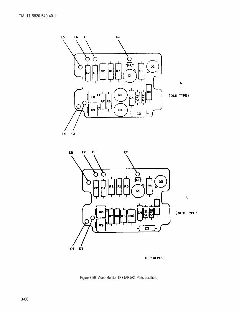
TM 11-5820-540-40-1
Figure 3-59. Video Monitor 1RE1AR1A2, Parts Location.
3-86

TM 11-5820-540-40-1
Figure 3-60. Alarm Control 1RE1AR1A3, Printed Circuit Board
Figure 3-61. Alarm Control 1RE1AR1A3, Parts Location.
3-87

TM 11-5820-540-40-1
Figure 3-62. Video Amplifier 1RE1AR1AR1, Parts Location
Figure 3-63. High Pass Filter 1RE1AR1FL1, Printed Circuit Board.
3-88
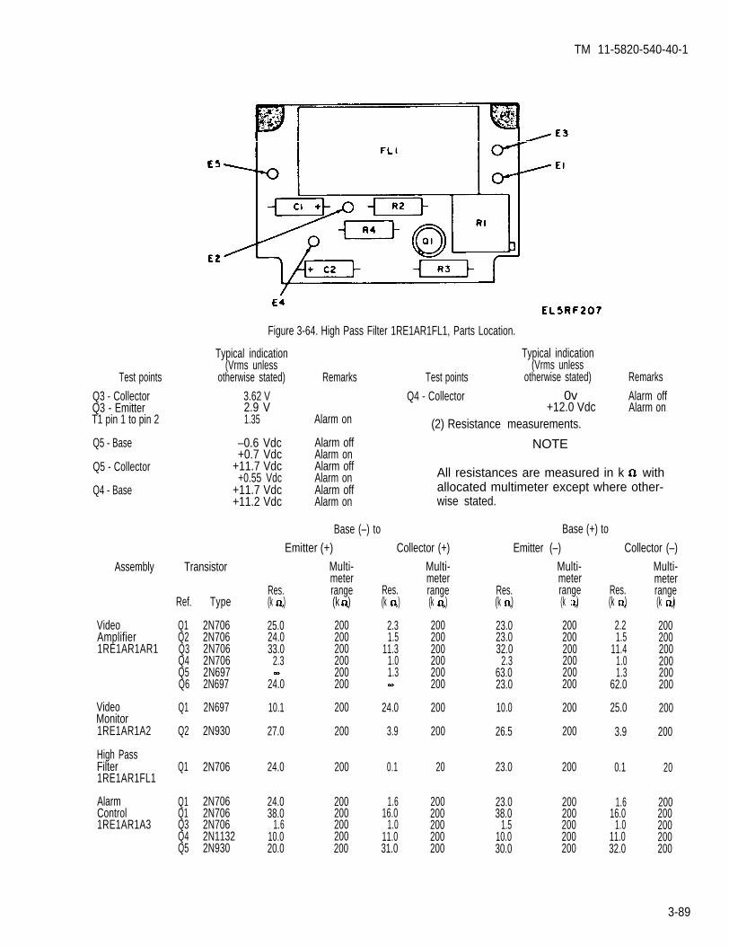
TM 11-5820-540-40-1
Figure 3-64. High Pass Filter 1RE1AR1FL1, Parts Location.
Typical indication(Vrms unless
otherwise stated)
Typical indication(Vrms unless
Test points otherwise stated) RemarksTest points
Q3 - CollectorQ3 - EmitterT1 pin 1 to pin 2
Remarks
3.62 V2.9 V1.35
Q4 - Collector 0v Alarm off+12.0 Vdc Alarm on
(2) Resistance measurements.Alarm on
Q5 - Base –0.6 Vdc+0.7 Vdc
+11.7 Vdc+0.55 Vdc
+11.7 Vdc+11.2 Vdc
Alarm offAlarm onAlarm offAlarm onAlarm offAlarm on
NOTE
Q5 - Collector All resistances are measured in k withallocated multimeter except where other-wise stated.
Q4 - Base
Base (–) to Base (+) to
Emitter (+) Collector (+) Emitter (–) Collector (–)
Multi-meterrange(k )
Multi-meterrange(k )
Assembly Transistor Multi-meterrange(k )
Multi-meterrange(k )
Res.(k )
Res.(k )
Res.(k )
Res.(k )Ref. Type
VideoAmplifier1RE1AR1AR1
Q1Q2Q3Q4Q5Q6
Q1
Q2
Q1
Q1Q1Q3Q4Q5
2N7062N7062N7062N7062N6972N697
2N697
2N930
2N706
2N7062N7062N7062N11322N930
25.024.033.0
2.3
24.0
10.1
27.0
24.0
24.038.0
1.610.020.0
200200200200200200
200
200
200
200200200200200
2.31.5
11.31.01.3
24.0
3.9
0.1
1.616.0
1.011.031.0
200200200200200200
200
200
20
200200200200200
23.023.032.0
2.363.023.0
10.0
26.5
23.0
23.038.0
1.510.030.0
200200200200200200
200
200
200
200200200200200
2.21.5
11.41.01.3
62.0
25.0
3.9
0.1
1.616.0
1.011.032.0
200200200200200200
200
200
20
200200200200200
VideoMonitor1RE1AR1A2
High PassFilter1RE1AR1FL1
AlarmControl1RE1AR1A3
3-89

TM 11-5820-540-40-1
3-14. Intermediate Frequency Amplifier1RE1AR2
a. Test Equipment and Material Required.Equipment Common name
Test Facility Receiver Receiver test facilityTS2867(V)2/GRM-95(V)2
Accessory Kit, Test Facilities Set Accessory kitMK-1173(V)2/GRM-95(V)2
Test Facility, RF Modules Rf modules test facilityTS-3837(V)2/GRM-95(V)2
Wattmeter HP-435A Power meterPower Sensor HP-8481A Power sensorDigital Multimeter AN/USM-451 Digital multimeterRf Voltmeter ME-426/U Rf voltmeter
b. Test Procedure.(1) Connect the test equipment as shown in figure
3-65. Set the power supply to 115 Vac as indicated onits panel voltmeter.
(2) Set the test facility switches as follows:Switch Position
S1 ONS14 30 MHzS9 30 MHzAttenuator AT1 30 dBS13 AGC
(3) Set the 10 dB step attenuator to maximumattenuation and the 1 dB step attenuator to 10 dB.
(4) On the test facilty, set S12 to AMPL IF.(5) Reduce the 10 dB step and 1 dB step
attenuators until the power meter reads —10 dBm±0.5 dBm. The attenuators should be set within therange of 22 to 32 dB, indicating and if. amplifier gain ofbetween 45 dB and 55 dB.
(6) Set S14 to 29 MHz and then to 31 MHz. Thepower meter reading should not vary by more than 3dB and should be within ±1.5 dB of the reading set in(5) above.
(7) Reset S14 to 30 MHz and set 10 dB stepattenuator to 10 dB and 1 dB step attenuator to 0 dB.Power indication should be within the range of –1.5dBm to –4.5 dBm.
(8) Increase the 1 dB step attenuator to 5 dB. Setthe digital multimeter to 20 volt dc range and connectto pin 6 (+) and pin 3 (–) to J35 on test facility. Notethe AGC voltage reading.
(9) Increase the 10 dB step attenuator to 20 dB.Measure the AGC voltage. It should have changed bymore than 0.1 V.
C. Troubleshooting. (FO-21)Symptom Probable cause Checks and corrective measures
1. Step b (5) and (6) above: low or no a. Loss of agc voltage. a.output.
b. One or more defective amplifier cord- b.wood modules.
Set the test facility switch S13 to MANand the AGC GAIN control to minimum(fully CCW). Check for–11 Vdc at thefollowing points: E6 and E3(1RE1AR2AR5) (fig. 3-66) E3(1RE1AR2AR2) and E2(1RE1AR2AR1). Replace the cordwoodmodule through which age is not beingpassed
Set test facility attenuator AT1 to 30 dBand the AGC GAIN control to maxi-mum (fully CW). Using rf voltmeter,check in turn the output of each cord-wood module at the points indicatedbelow with attenuator AT1 set asfollows
AT1 NormalTest points setting indication
(dB) (mvrms)
E4(1RE1AR2AR1) 30 75E5(1RE1AR2AR2) 30 225E4(1RE1AR2AR3) 40 350E5(1RE1AR2AR5) 40 450
Replace the cordwood module with abnormaloutput indication.
2. Step b (8) above: No agc action Defective cordwood module 1RE1AR2A1. Replace 1RE1AR2A1 and repeat test pro-cedure b.
3-90

TM 11-5820-540-40-1
Figure 3-65. Intermediate Frequency Amplifier 1RE1AR2, Test Setup.
3-91

TM 11-5820-540-40-1
Figure 3-66. Intermediate Frequency Amplifier 1RE1AR2, Cover Removed
d. Resistance Measurements.(1) Disconnect intermediate frequency amplifier
1RE1AR2 from the test equipment(2) Set the digital multimeter to 200 k .(3) Measure the resistance as indicated below.
Test points
1RE1AR2AR1Q1 (fig. 3-67)Emitter (+) Collector (–)Base (–) Emitter (–)Base (–) Collector
1RE1AR2A1Q1 (fig. 3-68Emitter (+) Collector (–)Collector (+) Emitter (–)Emitter (+) Base (–)Base (+) Emitter (–)Collector (+) Base (–)Base (+) Collector (–)
Typical resistance(k )
4
4.43
111312803080
Test points Typical resistance(k )
1RE1AR2AR3Q1 (fig 3-69)Emitter (+) Collector (–) 3Base (+) Emitter (–) 80Base (+) Collector (–) 80
1RE1AR2AR5Q1 (fig. 3-70)Collector (+) Emitter (–) 3.8Emitter (+) Base (–) 3.8Collector (+) Base (–) 3.1
3-15. Bandpass Filter, 1RE1FL1
a. Test Equipment Required.Equipment Common name
Test Facility, Receiver Receiver test facilityTS-2867(V)2/GRM-95(V)2
Generator, Signal HP-8640B Signal generatorPower Meter HP-435A Power meterSensor, Power HP-8484A Power sensorAttenuator, Fixed CN-1286/U (2 ea.) 10 dB attenuator
(3AT4) (4AT1)
3-92

TM 11-5820-540-40-1
Figure 3-67. Intermediate Frequency Amplifier 1RE1AR2AR1, Test Point Location.
3-93

TM 11-5820-540-40-1
3-94
Figure 3-68. Radio Frequency Detector 1RE1AR2A1, Test Point Location.

TM 11-5820-540-40-1
Figure 3-69. Intermediate Frequency Amplifier 1RE1AR2AR3, Test Point Location.
3-95
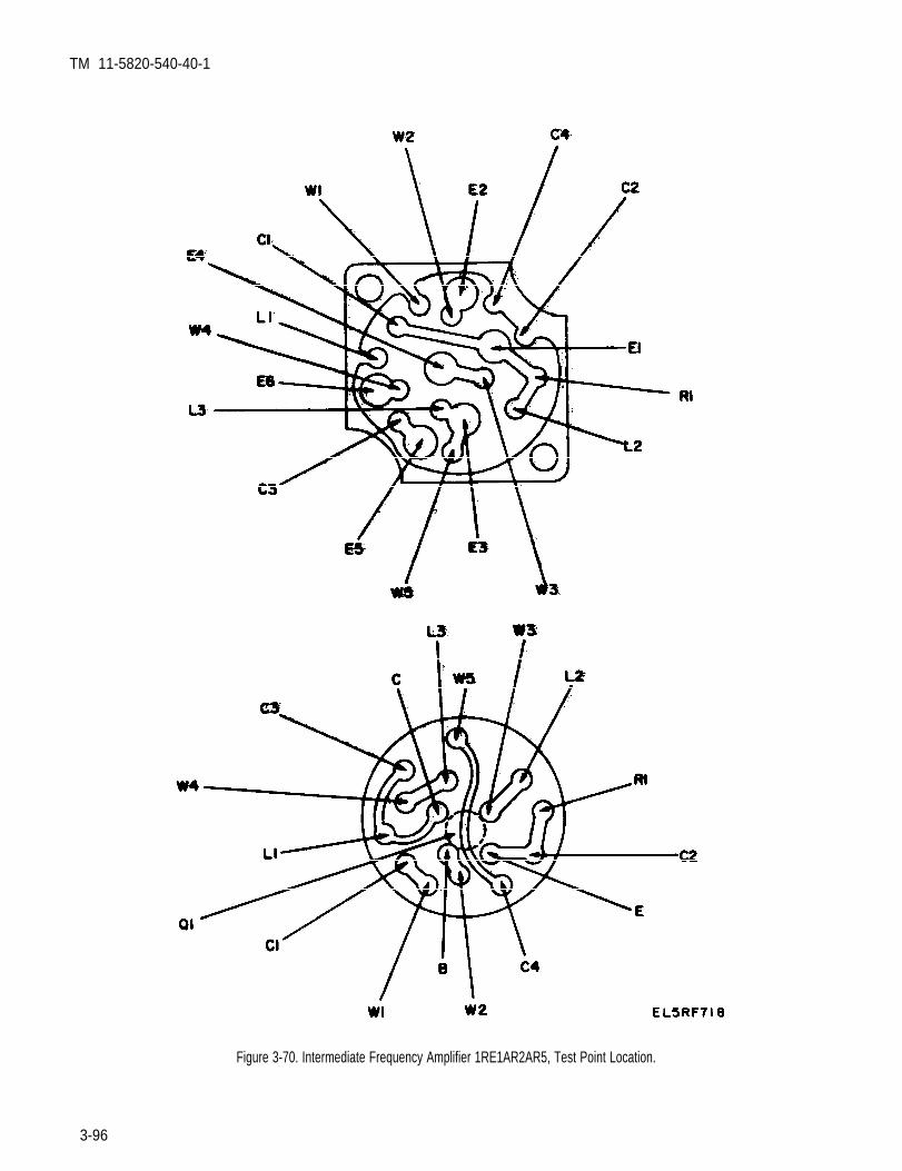
TM 11-5820-540-40-1
Figure 3-70. Intermediate Frequency Amplifier 1RE1AR2AR5, Test Point Location.
3-96

TM 11-5820 -540-40-1
b. Test Procedures.(1) Connect the test equipment
figure 3-71.(2) Adjust the signal generator
quency of 30 MHz, at an output levelindicated on the power meter.
(3) Connect the test equipment
as shown in A,
for a CW fre-of —30 dBm as
to the UUT asshown in B, figure 3-71. Fine tune the signal generatorfrequency for a maximum indication on the powermeter. The frequency read on the frequency counter ofthe signal generator shall be 30 MHz ±5O kHz. Notethe frequency.
(4) The power meter shall indicate –42 dBmminimum (equivalent to a maximum insertion loss of12 dB). Note the power meter indication.
(5) Adjust the signal generator to the frequencieslisted below. Subtract the power meter indication foreach frequency from the power meter indication notedin (4) above, to obtain the frequency response. Theresults should be within the attenuation (dB) limitsspecified below.
Signal generator frequency Relative attenuation (dB) fromreference frequency ((3) above), reference ((4) above).+/– frequency below. Minimum Maximum
–360 kHZ 2.40 3.00+360 kHz 2.50 3.10–600 kHZ 7.00 8.40+600 kHZ 7.10 8.50–840 kHZ 14.00 18.00+840 kHz 13.00 17.00–960 kHZ 18.50 24.50+960 kHz 15.50 21.50
c. Troubleshooting.If bandpass filter 1RE1FL1 fails either the insertionloss or frequency response tests in b. above, replace itDispose of the defective filter according to localregulations.
3-16. Receiver Case 1A2NOTE
The following procedure checks the con-tinuity and ground connections of the inter-connecting cable between the receiver fixedhead and the receiver rf head.
Test Equipment and Material Required.
Equipment Common name
Test Facility Transmitter Transmitter test facilityTS-2866(V)2/GRM-95(V)2
Accessory Kit, Test Facilities Set Accessory kitMK-1173(V)2/GRM-95(V)2
Equipment Common name
Digital MultimeterAN/USM-451 Digital multimeterExtractor TOOl, Cannon CET C6B Extractor ToolInsulation Tester GR 1864 Megohmmeter
b. Test Procedures.(1) Interconnecting wiring tests.
(a) Connect the equipment as shown in A,figure 3-72. (b) Set transmitter test facilityswitches S1 and S6 to ON.
(c) Set test set S1 to positions 1 through 29.For each position of S1 rotate S2 to positions 1through 35, the test lamp shall light whenever S2 posi-tion matches S1 position and whenever S2 is in posi-tion 30 through 35.
(d) Set transmitter test facility switches S1 andS6 to OFF and disconnect the test set.
(2) Continuity tests.Use the DMM to perform continuity tests of the con-nections listed below.
J9-1 to J2-C (OW)-2 -D-4 -A-5 -B-14 -E-8 -F-8 J1-B-8 (115 Vat)-6 -A-7 -c
J9-5 to J3-C-11 -D-10 -A-8 -B-9 J7 (TMG)-13 J6 (PCM)-12 J5 (130 Ohms) (VIDEO)
-12 J4 (51 Ohms) (FDM)J5 pin to ground (68 ohms)
(3) Insulation test, wire to wire
WARNING
HIGH VOLTAGE is accessible at the con-nectors and test leads of the megohmmeter.Ensure that the test switch is in the“DISCHARGE” position before handlingtest connections.
(a) Connect the test equipment as shown in B,figure 3-72.
(b) Set the megohmmeter controls to“measure” and “200 volts”.
(c) Set S2 (test set) to positions 1 through 29.For each position of S2 Rotate S1 through a completerevolution.
(d) The megohmmeter shall indicate more than100 megohms EXCEPT when S1 and S2 poistionsmatch.
(e) Set the megohrnmeter to DISCHARGE andOFF and disconnect the test set and cables fromreceiver case 1A2.
3-97

TM 11-5820-540-40-1
Figure 3-71. Bandpass Filter 1RE1FL1, Insertion Loss and Frequency Response Measurement, Test Setup.
(f) Connect the (+) and (GND) terminals of themegohmmeter to receiver case 1A2 with test lead CX-12044/U(1W36). Be sure that a good electrical con-nection is made.
(g) Connect test lead CMC 267-800020-000(4W16) to the megohmmeter (–) terminal.
WARNING
When performing the following procedure,set the megohmmeter controls to ON, 200V and MEASURE, only after making a con-nection. Set the megohmmeter to DIS-CHARGE before changing a connection.
(h) Use test lead to check insulation resistancebetween J9 pins 1 through 7,9, 10, 11, 13, 14, A1 cen-ter contact, A2 center contact and GND. The
megohmmeter should indicate greater than 100megohms for each check.
(i) Set the megohmmeter to OFF and discon-nect the test setup.
(4) Checking depth of connectors(a) Use Fixed depth Gage TL-776 to check the
proper depth of connectors J7 and J8. With the top ofthe gage resting on the front edges of the case, the bot-tom of the gage should barely touch the connectors.Install locally manufactured shims under the retainingplate when this cannot be attained.
(b) Use Fixed Depth Gage TL-767 to check theproper depth of connector J10. With the top of thegage resting on the front edges of the case, the bottomof the gage should barely touch the mounting flanges ofJ10. Install washers between the flange and the casewhen this cannot be attained.
3-98

TM 11-5820-540-40-1
Figure 3-72. Reciever Case Continuity Check, Test Setup.
c. Repairs. applicable, and paragraph 2-10 for replacement of con-If an abnormal indication is obtained in the test above, nectors. To remove rf connectors A1 and A2 ofremove the distribution box and cable assembly as 1A2A1J9, extractor tool Cannon CET C6B isdescribed in paragraph 2-25. Refer to FO-1 or FO-2, as required. Insulation test failures may be caused byapplicable, and schematic for interconnecting box test contaminants in the cabling and connectors.set TS-2870/GRM-95(V) (TM 11-6625-1696-14) to Thoroughly clean and dry the distribution box, cables,identify faulty connections. Refer to FO-1 or FO-2, as and connectors and retest.
Section II. TRANSMITTER RADIO FIXED HEAD
(TRANSMITTER, RADIO T-983 (P)/GRC-103(v),
T-983A(P)/GRC-103(V), OR T-983B(P)/GRC-103(V))
NOTE 3-17. Transmitter, Radio T-983(P)/GRC-103(V),T-983A(P)/GRC-103(V) or
Reference is to both units unless otherwise T-983B(P)/GRC-103(V)specified in the test. a. Test Equipment and Material Required.
3-99
TM 11-5820-540-40-1
Equipment
Test Facility, TransmitterTS-2866(V)2/GRM-95(V)2
Accessory Kit, Test Facilities SetMK-1173(V)2/GRM-95(V)2
Selective Voltmeter TS-3066(V)3/UDistortion Analyzer AN/URM-184AVoltmeter, Electronic ME-459/UGenerator, Signal HP 8640BGenerator, Signal AN/USM-205ACounter, Electronic, Digital Readout
TD-1225(V)1/UDigital Multimeter AN/USM-451Wattmeter HP-435APower sensor HP-8481A
Common name
Transmitter test facility
Accessory kit
Level meterDistortion analyzerVTVMSignal generatorWide range oscillatorCounter
Digital multimeterPower meterPower sensor
b. Test Procedure.(1) Operational check.
(a) Perform the following preliminary tests.1. Test electrical frequency synthesizer
5TR1A2 as described in paragraph 3-21 b. (7) (SM-D-698145) or paragraph 3-22 b. (7) (SM-D-865030).Refer to TM 1-5820-540-30 for synthesizer removaland replacement instructions.
2. Test amplifier monitor 5TR1A5 as de-scribed in paragraph 3-25. Refer to TM 11-5820-540-12 for removal and replacement instructions.
3. Test power supply 5TR1PS1 as describedin paragraph 3-26. Refer to TM 11-5820-540-30 forremoval and replacement instructions.
NOTE
Position the air outlet so that the air flow isdirected over the power supply heat sink.
(b) Connect the test equipment as shown in&figure 3-73. Set PP-6304 to ON and 115 Vat. Maintainthis voltage unless otherwise noted. Set test facilityswitches as follows:
Switch Position
S1 ONS20 S21S21 +28 V
PWR ALM SET LEVEL Fully CCW
(c) Switch on the unit under test and check forthe following:
1. AC POWER lamp should light.2. LOW POWER lamp should light.3. Set S17 to ON and S18 to 58.25. SYNC
lamp may light and should go out within 10 seconds.4. Buzzer should sound. If buzzer doesn’t
sound, push BUZZER OFF button. If buzzer still doesnot sound, check setting of BUZ OFF/ALM NORswitch.
(d) Press S24 on the test facility. The OVER-HEAT alarm lamp on the unit under test should light.
(e) On the unit under test, set the BUZZEROFF/ALARM NORMAL switch (mounted on rear ofcontrol panel) to the BUZZER OFF position. The buz-zer should be silent and all alarm lights should dim.
(f) Return the switch to ALARM NORMAL. The buzzer should sound and alarm lamps brighten.
(g) Press the BUZZER OFF button on the unitunder test to silence the buzzer.
(h) Set test facility switch S22 to TEST. Thedigital multimeter should indicate 14 Vac +1.4 V.Release S22.
(i) Connect the counter to connectors J24 andJ29 as shown in C, figure 3-73.
(j) Set test facility switch S22 to TEST. Thecounter should indicate 400 Hz ±40 Hz. Release S22.
(k) Set switch S21 to OFF. Press and hold S23.Set S21 to +600 V. Test facility meter Ml should indi-cate in the green band.
(l) Connect the test equipment as shown infigure B, figure 3-73.
(m) Set the wide range oscillator to 10 kHz at alevel of 705 mvrms as indicated on the VTVM.
(n) Check the metering on the unit under test.(o) Indications should be as shown in chart
below.
Meter position Indication
12 Vdc Within green band28 Vdc Within green bandOSC Between 20 and 90 percent of full scaleDOUBLER Between 20 and 90 percent of full scaleMULT ZeroDRIVER ZeroPWR OUT ZeroREFL PWR Zero12 CHPCM Within green band using INPUT con-
trol on unit under test.24 CHPCM As above.FDM As above.
NOTE
If abnormal indications are obtained in anyof the above tests, carry out the trouble-shooting procedures (c below).
(2) Deviation check.(a) Connect the test equipment as shown in B,
figure 3-73.(b) Set the signal generator frequency to
146.50 MHz and the wide range oscillator to 10 kHz at705 mvrms.
(c) Set test facility switch S20 to the 30 MHz DISCR position.
3-100
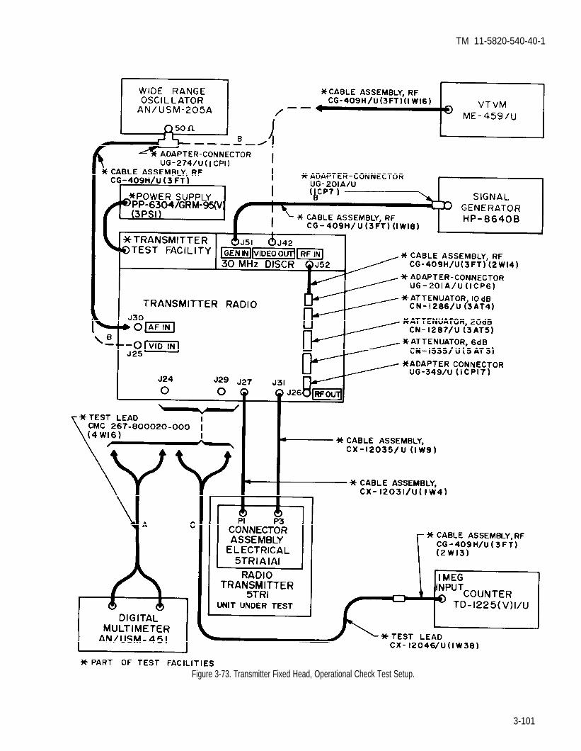
TM 11-5820-540-40-1
Figure 3-73. Transmitter Fixed Head, Operational Check Test Setup.
3-101

TM 11-5820-540-40-1
(d) Adjust the signal generator output level foran indication of 50 percent of full scale on test facilitymeter MI.
(e) Adjust the signal generator frequency untiltest facility meter M2 indicates zero (at center).Recheck the signal level on Ml. If necessary readjustthe output level of the signal generator for a 50 percentof full scale indication.
(f) Set test facility switch S21 to O dB position.(g) On the unit under test, set the meter selec-
tor switch to 24 CH PCM and adjust the INPUT con-trol so that meter indicates exactly 50% full scaledeflection.
(h) Connect the VTVM to J42 on the testfacility. The VTVM should indicate between 130 and193 mVrms.
(j) Tune the wide range oscillator to 1.0 kHzand set the meter switch on the unit under test to FDMposition.
(k) On the unit under test, adjust the INPUTcontrol so that the meter indicates exactely 50% fullscale deflection. The VTVM should indicate between33 and 48 mVrms.
(1) Connect the wide range oscillator to J30 AFIN connector to the transmitter test facility and theVTVM to the UG274/U connector at the output of thewide range oscillator.
(m) Set the wide range oscillator to 1.0 kHz andadjust its output level to 245 mVrms (– 10 dBm into600 ) indicated on the 600 scale of the VTVM.
(n) Connect the VTVM to connector J42; theVTVM should indicate between 19 and 29 mVrms.
NOTE
If due to residual fm on the unit under testthe deviation cannot be measuredaccurately, increase the level of the testsignal to +2.0 dBrn. This should give andindication of between 76 and 116 mVrms atJ42.
(o) If the results in (h), (i), (k), and(n) above arenot as specified, check electrical frequency synthesizer5TR1A2 (para. 3-21).
(3) Deviation attenuator check.(a) Using the test setup shown in B, figure 3-73,
connect the wide range oscillator to VID IN connectorJ25 on the test facility.
(b) Set the wide range oscillator to 10 kHz at alevel 705 mVrms.
(c) On the unit under test set the INPUT con-trol to obtain a 200 mVrrns indication on the VTVMconnected to connector J42.
3-102
(d) Check the remainingS21 as shown in the chart below.
positions of switch
Test Facility switch positions VTVM indicationS18 S21 (Millivolts rms)
58.25 6 dB 100 ±358.25 12 dB 50 ±261.66* 3.5 dB 133±1161.66* 9.5 dB 67 ±6
*Set the signal generator to 153.333 MHz using procedure des-cribed in (2)(d) and (e) above and repeat steps (3)(a) through (c).
(4) Power output and frequency check.(a) Readjust signal generator as in (2) (d) and
(e) above. Connect the test equipment as shown infigure 3-74.
(b) Set switch S21 to the +28 V position andS17 to ON. The power meter connected at J26 shouldindicate not less than +4 dBm for all positions of testfacility switch S18.
(c) On the unit under test, check the meterindication at the OSC and DOUBLER positions for allpositions of switch S18. The meter should indicatebetween 20 and 90 percent of full scale deflection.
(d) Replace the power meter at connector J26with the counter.
(e) Check the frequency at all positions ofswitch S18. The indications should be as shown in thechart below.
S18 position
47.5048.3350.6552.3154.9858.2561.6663.4666.0067.5072.50
Frequency (MHz ±0.001%)T-983(P) T-983A(P) or T-983B(P)
95.00000096.666666
101.312500104.625000109.958330116.500000123.333330126.937500132.000000135.000000145.000000
95.00000096.687500
101.312500104.656250109.958330116.531250123.333333126.968750132.000000135.020834145.000000
(5) Low power alarm check.(a) Connect the test equipment as shown in
figure 3-75.(b) Rotate the PWR ALM SET LEVEL con-
trol on the test facility until the LOW POWER alarmlamp on the unit under test goes out The digitalvoltmeter should indicate 130 mV ±20 mV.
(c) Rotate the PWR ALM SET LEVEL con-trol on the test facility until the LOW POWER alarmlamp on the unit under test lights. The digitalvoltmeter should indicate 80 mV ±5 mV.

TM 11-5820-540-40-1
Figure 3-74. Transmitter Fixed Head Power Output and Frequency Check, Test Setup.
(6) Video frequency response testing.(a) Connect the test equipment as shown in A,
figure 3-76.(b) Set the coaxial switch to position 2.(c) Set S21 to +28 V and S20 to 30 MHz
DISCR. Set unit under test power to ON. Set S17 toON and S18 to 58.25.
(d) Tune the signal generator to 146.5 MHzand adjust the output level for a 50 percent of fullscale indication on test facility meter M1.
(e) Adjust the signal generator frequency untiltest facility meter M2 indicates zero (at center).
Recheck the signal level on M1; if necessary readjustthe output level of the signal generator for a 50 per-cent of full scale indication
(f) On the unit under test, set the meteringswitch to the 12 CHPCM position.
(g) On the unit under test, set the INPUT con-trol to midrange.
(h) Tune the wide range oscillator to 10 kHzand adjust the output level for a 25 percent of fullscale indication on the meter of the unit under test
(i) Check the signal-to-noise ratio as describedbelow.
3-103

TM 11-5820-540-40-1
Figure 3-75. TransmitterFixed Head Low Power Alarm Check, Test Setup.
1. Tune the wide range oscillator to 960kHz.
2. Adjust the level meter to 960 kHz andrecord the indication.
3. Disconnect the wide range oscillator andincrease the gain of the level meter by 20 dB. Theindication should not excced that obtained in 2 above.
NOTE
During the following test do not disturbthe INPUT control on the unit under test.
(j) Tune the wide range oscillator to 10 kHz asread on the counter.
(k) Adjust the level meter to 10 kHz andrecord the indication Use unbalanced 50 input
(l) Set the coaxial switch to position 1.
(m) Adjust the variable attenuators to obtain -
the same indication as that obtained in (k) above.Record the attenuator settings. This is the referencelevel.
(n) Set the coaxial switch to position 2.
3-104
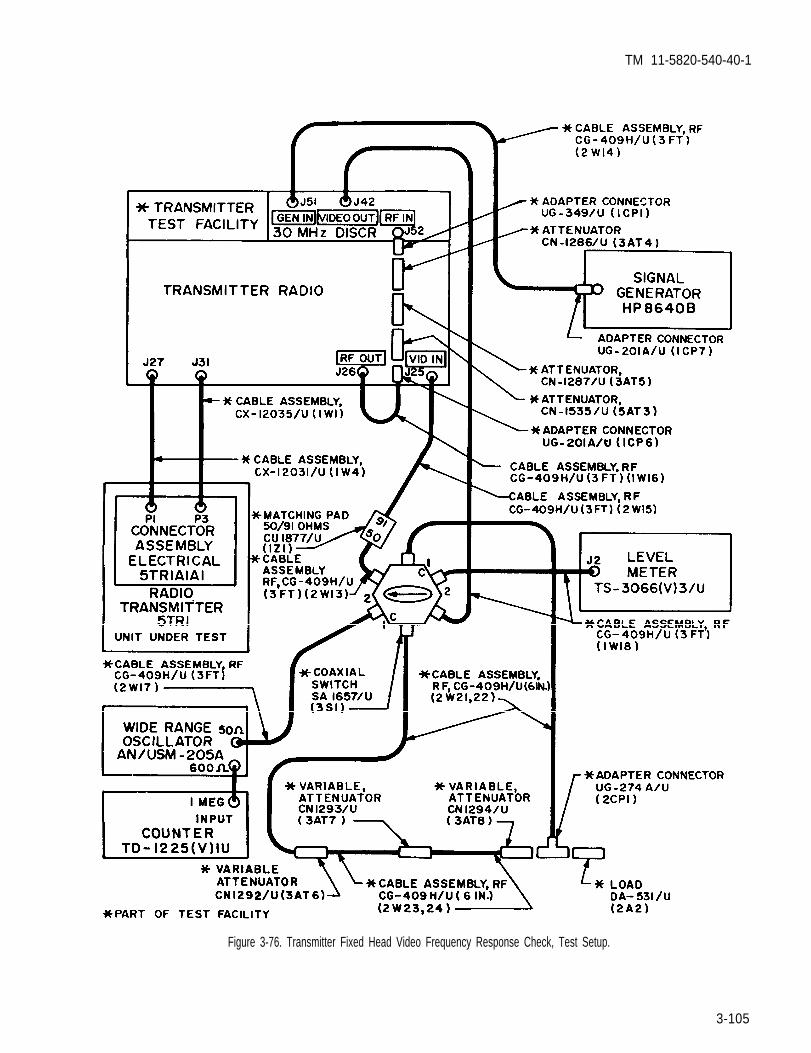
TM 11-5820-540-40-1
Figure 3-76. Transmitter Fixed Head Video Frequency Response Check, Test Setup.
3-105
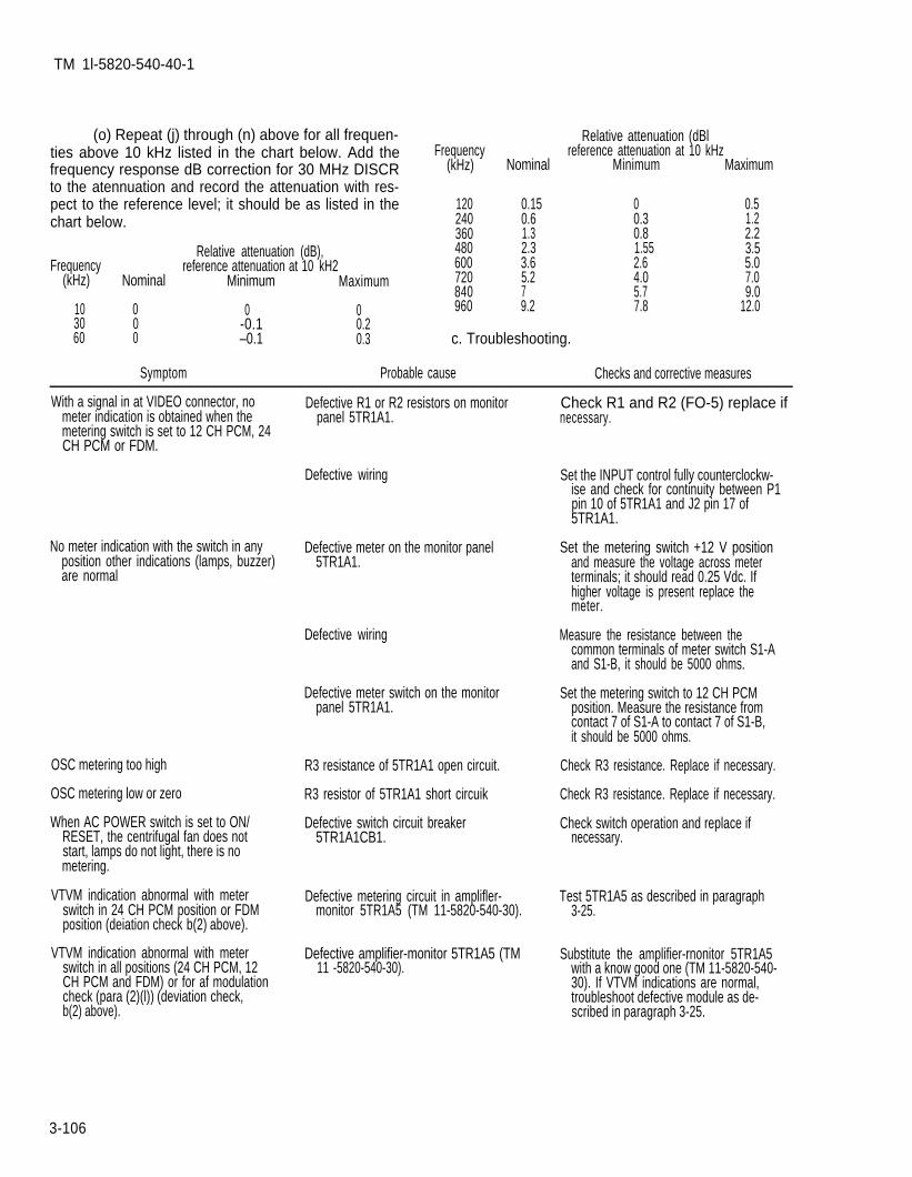
TM 1l-5820-540-40-1
(o) Repeat (j) through (n) above for all frequen-ties above 10 kHz listed in the chart below. Add thefrequency response dB correction for 30 MHz DISCRto the atennuation and record the attenuation with res-pect to the reference level; it should be as listed in thechart below.
Relative attenuation (dBlreference attenuation at 10 kHz
Minimum MaximumFrequency
(kHz) Nominal
120240360480600720840960
0.150.61.32.33.65.279.2
00.30.81.552.64.05.77.8
0.51.22.23.55.07.09.0
12.0
Relative attenuation (dB),Frequency reference attenuation at 10 kH2
(kHz) Nominal Minimum Maximum
10 0 0 030 0 -0.1 0.260 0 –0.1 0.3 c. Troubleshooting.
Symptom Probable cause Checks and corrective measures
With a signal in at VIDEO connector, no Defective R1 or R2 resistors on monitormeter indication is obtained when the panel 5TR1A1.metering switch is set to 12 CH PCM, 24CH PCM or FDM.
Check R1 and R2 (FO-5) replace ifnecessary.
Defective wiring Set the INPUT control fully counterclockw-ise and check for continuity between P1pin 10 of 5TR1A1 and J2 pin 17 of5TR1A1.
No meter indication with the switch in any Defective meter on the monitor panelposition other indications (lamps, buzzer) 5TR1A1.are normal
Set the metering switch +12 V positionand measure the voltage across meterterminals; it should read 0.25 Vdc. Ifhigher voltage is present replace themeter.
Defective wiring Measure the resistance between thecommon terminals of meter switch S1-Aand S1-B, it should be 5000 ohms.
Defective meter switch on the monitorpanel 5TR1A1.
Set the metering switch to 12 CH PCMposition. Measure the resistance fromcontact 7 of S1-A to contact 7 of S1-B,it should be 5000 ohms.
OSC metering too high R3 resistance of 5TR1A1 open circuit. Check R3 resistance. Replace if necessary.
OSC metering low or zero R3 resistor of 5TR1A1 short circuik Check R3 resistance. Replace if necessary.
When AC POWER switch is set to ON/RESET, the centrifugal fan does notstart, lamps do not light, there is nometering.
Check switch operation and replace ifnecessary.
Defective switch circuit breaker5TR1A1CB1.
VTVM indication abnormal with meterswitch in 24 CH PCM position or FDMposition (deiation check b(2) above).
Defective metering circuit in amplifler- Test 5TR1A5 as described in paragraphmonitor 5TR1A5 (TM 11-5820-540-30). 3-25.
VTVM indication abnormal with meterswitch in all positions (24 CH PCM, 12CH PCM and FDM) or for af modulationcheck (para (2)(l)) (deviation check,b(2) above).
Defective amplifier-monitor 5TR1A5 (TM Substitute the amplifier-rnonitor 5TR1A511 -5820-540-30). with a know good one (TM 11-5820-540-
30). If VTVM indications are normal,troubleshoot defective module as de-scribed in paragraph 3-25.
3-106
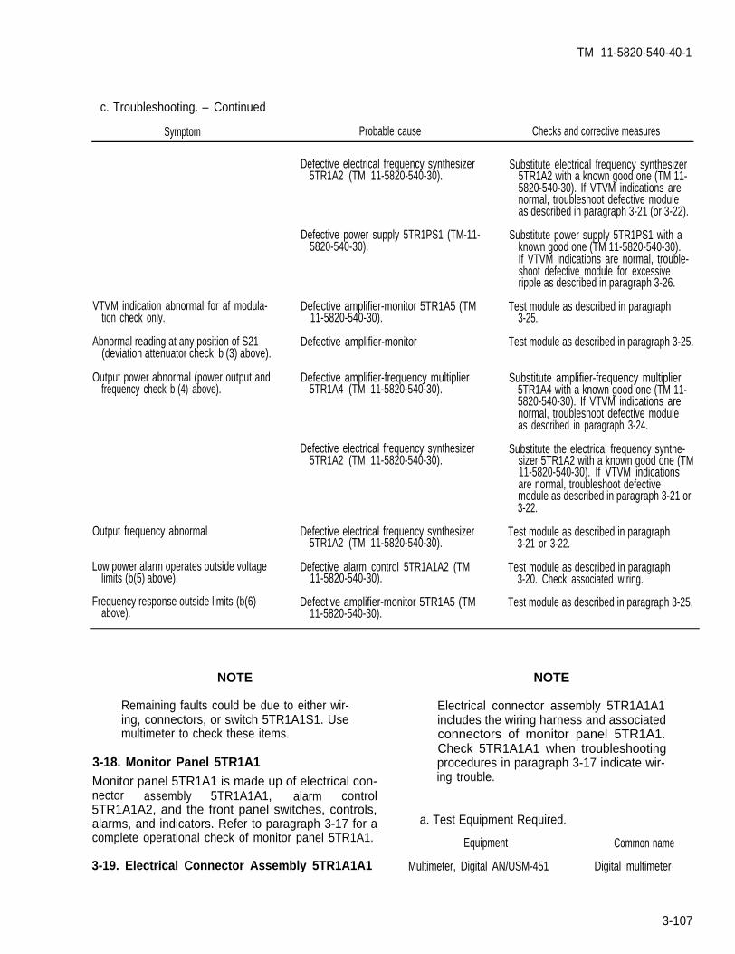
TM 11-5820-540-40-1
c. Troubleshooting. – Continued
Symptom Probable cause Checks and corrective measures
Defective electrical frequency synthesizer5TR1A2 (TM 11-5820-540-30).
Defective power supply 5TR1PS1 (TM-11-5820-540-30).
VTVM indication abnormal for af modula- Defective amplifier-monitor 5TR1A5 (TMtion check only. 11-5820-540-30).
Abnormal reading at any position of S21 Defective amplifier-monitor(deviation attenuator check, b (3) above).
Output power abnormal (power output and Defective amplifier-frequency multiplierfrequency check b (4) above). 5TR1A4 (TM 11-5820-540-30).
Defective electrical frequency synthesizer5TR1A2 (TM 11-5820-540-30).
Output frequency abnormal Defective electrical frequency synthesizer5TR1A2 (TM 11-5820-540-30).
Low power alarm operates outside voltage Defective alarm control 5TR1A1A2 (TMlimits (b(5) above). 11-5820-540-30).
Frequency response outside limits (b(6) Defective amplifier-monitor 5TR1A5 (TMabove). 11-5820-540-30).
Substitute electrical frequency synthesizer5TR1A2 with a known good one (TM 11-5820-540-30). If VTVM indications arenormal, troubleshoot defective moduleas described in paragraph 3-21 (or 3-22).
Substitute power supply 5TR1PS1 with aknown good one (TM 11-5820-540-30).If VTVM indications are normal, trouble-shoot defective module for excessiveripple as described in paragraph 3-26.
Test module as described in paragraph3-25.
Test module as described in paragraph 3-25.
Substitute amplifier-frequency multiplier5TR1A4 with a known good one (TM 11-5820-540-30). If VTVM indications arenormal, troubleshoot defective moduleas described in paragraph 3-24.
Substitute the electrical frequency synthe-sizer 5TR1A2 with a known good one (TM11-5820-540-30). If VTVM indicationsare normal, troubleshoot defectivemodule as described in paragraph 3-21 or3-22.
Test module as described in paragraph3-21 or 3-22.
Test module as described in paragraph3-20. Check associated wiring.
Test module as described in paragraph 3-25.
NOTE
Remaining faults could be due to either wir-ing, connectors, or switch 5TR1A1S1. Usemultimeter to check these items.
3-18. Monitor Panel 5TR1A1Monitor panel 5TR1A1 is made up of electrical con-nector assembly 5TR1A1A1, alarm control5TR1A1A2, and the front panel switches, controls,alarms, and indicators. Refer to paragraph 3-17 for acomplete operational check of monitor panel 5TR1A1.
3-19. Electrical Connector Assembly 5TR1A1A1
NOTE
Electrical connector assembly 5TR1A1A1includes the wiring harness and associatedconnectors of monitor panel 5TR1A1.Check 5TR1A1A1 when troubleshootingprocedures in paragraph 3-17 indicate wir-ing trouble.
a. Test Equipment Required.
Equipment
Multimeter, Digital AN/USM-451
Common name
Digital multimeter
3-107

TM 11-5820-540-40-1
Figure 3-77. Alarm Control 5TR1A1A2 or 1RE1A1A2, Parts Location.
b. Test Procedure. Refer to the transmitter intercon- Equipment Common namenection diagram, FO-5, and check continuity between Test Facility, Transmitter Transmitter test facilityassociated connector pins. Refer to paragraph 2-10 for TS-ZS66(Y)Z/GRM-95(V)Z.repair or replacement of connectors. Multimeter, Digital AN/USM-451 Digital multimeter
b. Test Procedure.(1) Use the multimeter to check resistance be-
3-20 Alarm Control 5TR1A1A2 or 1RE1A1A2 tween the terminal pins listed in the chart below. Refera. Test Equipment and Material Required. to figure 3-77 to locate the terminals.
3-108

TM 11-5820-540-40-1
Multimeter connections(+) (–)
otherwise indticated)
E1 E11E2 E4E2 E5E2 E12E4 E5E3 E6E3 E13E5 E4E5 E16E7 E9E7 E1OE8 E11E11 E1E11 E8E11 E14E11 E15E12 E4E12 E5E15 E11E16 E5E17 E18
* Digital multimeter
Resistance(ohms ±10% unless
*
*
**
*
*
Greater than 200k320 ±5%Greater than 200k640 ±5%Greater than 100k100 ±5%320 ±5%Less than 2kLess than 3kInfinityoGreater than 200kLess than 3kLess than 3k100Less than 3k320Greater than 200kGreater than 200kGreater than 200ko
(2) Connect the test equipment as shown in figure3-78.
(3) Set test facility switches S1, S6, and S17 totheir ON positions.
(4) Check the operation of relay K1 in the unitunder test; connect the power supply and measure theresistance between the testchart below.
Power supplyconnections
(+) (–)
E11 E1
E11 E8E11 E15
points as shown in the
connectmultimeterbetween
E7 and E1OE7 and E9E17 and E18E17 and E19E7 and E10E7 and E10
Resistance(ohms)
InfinityoInfinityoInfinityInfinity(1RE1A1A2only).
c. Troubleshooting (FO-5).
Symptom
Abnormal indication of any re-sistance measurement (b(1)above.)
Abnormal indication with powersupply (–) connected to E1,(b(4) above); other testsnormal.
Checks and correctivemeasures
Refer to FO-5 check com-ponents in defectivecircuit; replace com-ponents as required.
Check and replace diodeCR1 as required.
Symptom
Abnormal indication with powersupply (—) connected to E1 orE8 (b(4) above).
Abnormal indication with powersupply (–) connected to E8(b(4) above); other testsnormal.
Abnormal indication with powersupply (–) connected to E15(b(4) above); other tests
normal.
Checks and correctivemeasures
Check R7 and K1 relay;replace as required.
Check and replace diodeCR3 as required.
Check and replace diodeCR5 as required.
3-21. Electrical Frequency Synthesizer 5TR1A2or 1RE1A2 (SM-D-698145)
a. Test Equipment and Material Required.
Equipment Common name
Test Facility, Transmitter Transmitter test facilityTS-2866(V)2/GRM-95(V)2
Accessory Kit, Test Facilities Set, Accessory kit, testMK-1173(V)2/GRM-95(V)2 facility set
Multimeter, Digital AN/USM-451 Digital multimeterFrequency Meter TD-1224(V)1/U CounterGenerator, Signal HP 8640B Signal generatorPower Meter HP-435A Power meterPower Sensor HP-8481A Power sensorMeter, modulation ME-505/U Deviation meterVoltmeter, Electronic ME-459/U VTVMGenerator, Signal AN/USM-205A Wide range oscillatorDistortion Analyzer, AN/URM-184A Distortion analyzer
b. Test Procedure.
CAUTION
Removal and insertion of circuit boardswhile power is applied to the synthesizermay induce transient voltages which areharmful to certain components. Beforeremoving or inserting a board, set testfacility switch S17 to OFF.
(1) Preliminary setup.(a) Set the test facilty controls as follows:
Switch Position
S1 ONS18 72.50S20 S17
(b) Remove the synthesizer cover plate.(2) Field effect transistor operating voltage
adjustment.
3-109

TM 11-5820-540-40-1
Figure 3-78. Alarm Control 5TR1A1A2 or 1RE1A1A2, Test Setup.
NOTE
Remove signal data converter-storer board1RE1A2A8 or 5TR1A2A8 from the syn-thesizer. Pins 14 and 15 of the pc board areto be removed to prevent possible damageto the transmitter test facility TS-2866(V)2/GRM-95(V)2.
(a) Extend signal data converter-storer board1RE1A2A8 or 5TR1A2A8 from the synthesizer, usingextender board PL-1247/GRM-95 (V) as shown infigure 3-79 and set test facility control switch S17 toON.
(b) Connect the digital multimeter between pin4 of Q6 (+) and TP3 (–) of the extender board.
(c) If necessary, adjust R15 (fig. 3-80) on1RE1A2A8 or 5TR1A2A8 or 5TR1A2A8 until thedigital multirneter reads 11.5 V ±0.2 Vdc.
(d) Set switch S17 on the test facility to OFFand reinstall the extended board.
(3) Sync alarm test(a) Set test faciIity switch S18 to 66.00 and S17
to ALM 1. On the test facility, connect a jumper wirefrom pin 16 on J20 to the ground terminal next to J20.The SYNC lamp on the test facility should light andremain on (may blink once).
(b) Set test facility switch S17 to the ON posi-tion. The SYNC lamp should extinuish and remain out
(c) If necessary adjust R3 (fig. 3-81) on amp.-monitor board 1RE1A2A3 or 5TR1A2A3 to meet therequirements of (a) and (b) above.
(d) Set switch S17 to ALM 2. After a delay, theSYNC lamp should light and remain on.
(e) Set S17 to the ON position and remove thejumper from pin 16 of J20. The SYNC lamp shouldextinguish and remain out.
(f) Set S17 to OFF and remove rf oscillator board 1RE1A2Y1 or 5TR1A2Y1.
(g) Set S17 to ON. The SYNC lamp shouldlight.
(h) Set S17 to OFF and reinstall the rf oscillator board.
3-110

TM 11-5820-540-40-1
Figure 3-79. Field Effect Transistor, Operating Voltage Adjustment, Test Setup.
(4) Frequency check.(a) Connect the test equipment as shown in
figure 3-82.(b) On the test facility, set switches S17 to on
and S 18 to each position in chart below. The countershould indicate the frequencies listed for each portion.
S18 Position Freq (MHz) +Tolerance (Hz)
47.50 47.50 47554.98 54.979165 54963.46 63.46875 63472.50 72.50 725
NOTE
Due to residual fm, the output frequencieswill not be perfectly stable. Using a 1.0second count on the frequency counter, thefluctuations in frequency should be lessthan 200 Hz at 47.5 MHz and less than 400Hz at 72.5 MHz.
(c) Set switch S17 to OFF.
NOTE
If the output frequency is outside the limitsgiven in (b) above, proceed with (d) through(j) below.
(d) Extend RF oscillator board 1RE1A2Y1 or5TR1A2Y1 from the synthesizer using extenderboard, PL-1259/GRM-95(V) as shown in figure 3-83.
(e) Set switch S18 to 47.5 MHz.(f) Connect the counter between TP1 (–) of rf
oscillator 1RE1A2Y1 or 5TR1A2Y1 and TP3 (+) ofthe extender board.
(g) Set switch S17 to ON. The counter shouldindicate 500 kHz ±25 Hz.
(h) If necessary, adjust L1 (fig. 3-84) to obtainthe required frequency in (h) above.
(i) Set switch S17 to OFF and reinstall theextended board.
(j) Repeat (a) through (c) above. Observe thespecified tolerances.
3-111

TM 11-5820-540-40-1
Figure 3-80. Signal Data Converter-Storer 1RE1A2A8 or 5TR1A2A8, Parts Location
3-112

Figure 3-81.
TM 11-5820-540-40-1
Figure 3-82. Electrical Frequency Synthesizer 1RE1A2 or 5TR1A2 Frequency Check, Test Setup.
3-113

TM 11-5820-540-40-1
Figure 3-83. Rf Oscillator 1RE1A2Y1 or 5TR1A2Y1 Frequency Check, Test Setup.
(5) Power output and metering.(a) Connect the power meter to pin A1 of J11
on the synthesizer as shown in figure 3-85.(b) Set switch S17 to ON. Set switch S18 to all
on positions. Meter M1 should indicate between 20-80% of full scale and the power meter indicationshould be between +12 dBm and +17 dBm. Setswitch S17 to OFF.
(c) If power output is abnormal, remove thecover and extend modulator-oscillator board1RE1A2A2 or 5TR1A2 from the synthesizer usingextender board PL-1251/GRM-95(V)(3A5) figure 3-87.
NOTE
The extender board will cause a loss ofapproximately 1 dB. Verify output powerbefore and after adjustments with theextender board removed and 1RE1A2A12or 5TR1A2A2 reinstalled in thesynthesizer.
(d)minimum(b) above
(e)
Refer to figure 3-86 and adjust Cl 3 forpower meter fluctuation within the limts of
Replace the cover on modulator-oscillatorboard and reinstall it in the synthesizer.
(f) Repeat(b) above.(g) Set switch S17 to OFF.
(6) Deviation(a) Connect the test equipment as shown in
figure 3-88.(b) Set test facility switch S20 to 30 MHz
DISCR.(c) Set switch S18 to 47.50 and S17 to ON.(d) Set the signal generator frequency to 77.5
MHz at a level of 0 dBm. Fine tune the signalgenerator frequency to obtain a zero center indicationon test facility meter M2; readjust the signal generatoroutput level until meter M2 indicates 50 percent of fullscale deflection.
(e) Set switch S17 to the MOD ON position.The VTVM should indicate 50 Mv ±6 mV.
3-114

TM 11-5820-540-40-1
Figure 3-84. Rf Oscillator 1RE1A2Y1 or 5TR1A2Y1, Parts Location
(f) Repeat steps (c) through (e) for each fre-quency setting of S18. The signal generator will be setat 30 MHz above the S 18 frequency setting.
(g) If the requirements of (e) and (f) above arenot met proceed to (h) below.
NOTE
R9 controls overall deviation level. R6 is forfrequency compensation and will have agreater effect on deviation level at lowerfrequencies.
(h) Perform steps (c) through (f) above, adjust-ing R6 and R9 (fig. 3-86) at switch S 18 settings of 47.5and 72.5 respectively. Adjust for minimum overallvariation of VTVM indications from 50 mV at allswitch S18 settings.
(7) Modulation distortion check.(a) Connect the test equipment as shown in
figure 3-89.(b) set test facility switches S18 to 47.50 and
S17 to ON.(c) Set test facility switch S20 to 30 MHz
DISCR.
(d) Set the signal generator frequency to 77.5MHz at a level of 0 dBm. Fine tune the signalgenerator frequency to obtain a zero center indicationon test facility meter M2; readust the signal generatoroutput level until meter Ml indicates 50 percent of fullscale deflection.
(e) Set the wide range oscillator to 20 kHz andadjust the output level for an indication of 45 mV usingthe distortion analyzer, voltmeter function.
(f) Set the distortion analyzer to measure dis-tortion. The measured distortion shall not exceed 5percent.
(g) Set switch S17 to OFF.(8) Continuity test Using a digital multimter,
check for continuity between chassis ground and thefollowing points on the synthesizer P2 pin 4, J11 pin5, and J11 pin 2. (If digital multimter reads an open,check for broken or missing wires).
(9) Fault isolation procedure. If any of therequirements of (3) through (9) above are not met iso-late the fault in the following manner.
(a) Remove all boards from the synthesizer andinsert a complete set of known good boards.
(b) If the synthesizer still fails to function pro-perly, troubleshoot the synthesizer case (d. (2) below).
3-115
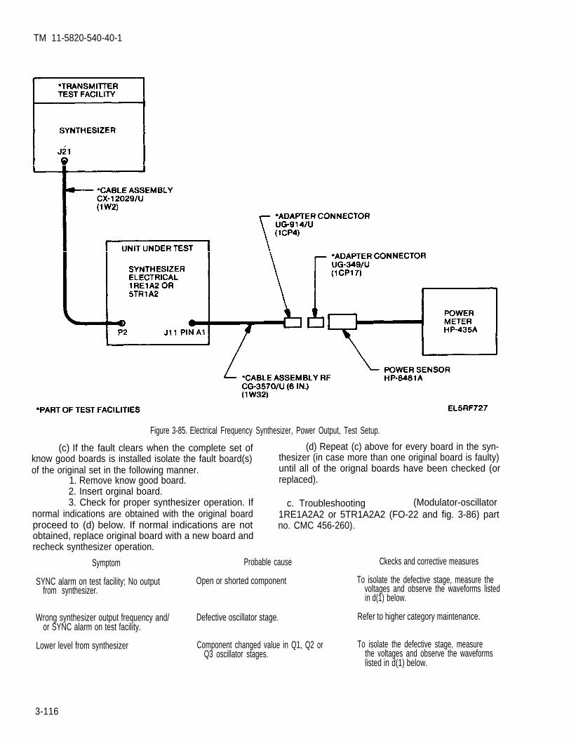
TM 11-5820-540-40-1
Figure 3-85. Electrical Frequency Synthesizer, Power Output, Test Setup.
(c) If the fault clears when the complete set of (d) Repeat (c) above for every board in the syn-know good boards is installed isolate the fault board(s) thesizer (in case more than one original board is faulty)of the original set in the following manner. until all of the orignal boards have been checked (or
1. Remove know good board. replaced).2. Insert orginal board.3. Check for proper synthesizer operation. If c. Troubleshooting (Modulator-oscillator
normal indications are obtained with the original board 1RE1A2A2 or 5TR1A2A2 (FO-22 and fig. 3-86) partproceed to (d) below. If normal indications are not no. CMC 456-260).obtained, replace original board with a new board andrecheck synthesizer operation.
Symptom Probable cause Ckecks and corrective measures
SYNC alarm on test facility; No output Open or shorted component To isolate the defective stage, measure thefrom synthesizer. voltages and observe the waveforms listed
in d(1) below.
Wrong synthesizer output frequency and/ Defective oscillator stage. Refer to higher category maintenance.or SYNC alarm on test facility.
Lower level from synthesizer Component changed value in Q1, Q2 or To isolate the defective stage, measureQ3 oscillator stages. the voltages and observe the waveforms
listed in d(1) below.
3-116

TM 11-5820-540-40-1
Figure 3-86. Modulator-Oscillator 1RE1A2A2 or 5TR1A2A2, Parts Location.d. Typical Voltage Measurements.
(1) Modulutor-oscillator 1RE1A2A2 or5TR1A2A2 (fig. 3-86), part No. CMC 456-260).
(a) Typical signal voltage indications using theallocated oscilloscope and test facility switch S18 at47.50:
NOTE
Replacement of Q1 or its circuit com-ponents will make complete realinement ofthe circuit board neccessary. Refer tohigher category maintenance for repair orrealinement
Typical indicationsTest points (volts ac peak-to-peak)
Q1 collector 2.6Q2 collector 0.8Q3 collector 9.0TP7 of extender board 4.0
(b) Typical dc voltage indications using thedigital voltmeter, with the synthesizer programed for47.5 MHz:
Typical indicationsTestpoints (volts dc)
Q2 base 0.76Q2 collector 1.60Q3 emitter 0.84Q3 base 1.58Q3 collector 1,20TP2(+) and TP3(-) of extender board 1.30
(2) Interconnecting box 1RE1A2A1A1 or5TR1A2A1A1 (fig. 3-90). Remove all plug-in circuitboards; set test facility switch S17 to ON. Check thevoltages between the following test points:
Typical indicationTestpoints (volts dc)
E30(+) to E9(–) 20E28(+) to E9(–) 16
3-117

TM 11-5820-540-40-1
Figure 3-87. Modulator-Oscillator 1RE1A2A2 or 5TR1A2A2, Varicap Turning Adjustment
3-22. Electrical Frequency Synthesizer5TR1A2 or 1RE1A2 (SM-D-865030)
b. Test Procedure.
CAUTIONa. Test Equipment Required.
Equipment Common name
Test Facility, TransmitterTS-2866(V)2/GRM-95(V)2
Accessory Kit, Test Facilities SetMK-1173(V)2/GRM-95(V)2
Multimeter, Digital AN/USM-451Frequency Meter TD-1225(V)1/UGenerator Signal HP-8640BPower Meter HP-435APower Sensor HP-8481AMeter, Modulation ME-505/UDistortion Analyzer, AN/U SM-184AVoltmeter, Electronic ME-459/UGenerator, Signal AN/USM-205ATest Lead CMC 267-800020-000Load, DA-531/U
Transmitter test facility
Accessory kit, testfacility set
Digital multimeterCounterSignal GeneratorPower meterPower sensorDeviation meterDistortion analyzerVTVMWide range oscillatorTest lead50 ohm dummy load
3-118
Removal and insertion of circuit boardswhile power is applied to the synthesizermay induce transient voltages which areharmful to certain components. Beforeremoving or inserting a board, set testfacility switch S17 to OFF.
(1) Preliminary setup.(a) Set the test facility controls as follows:
Switch Position
S1 ONS18 63.46S20 S17
(b) Remove the synthesizer cover plate.

TM 11-5820-540-40-1
Figure 3-88. Electical Frequency Synthesizer Deviation, Test Setup.
(2) Field effect transistor operating voltageadjustment
(a) Extend signal data converter-storer board1RE1A2A18 or 5TR1A2A19 from the synthesizer,using extender board PL-1257/GRM-95(V) as shownin figure 3-91, and set test facility control switch S17to ON.
(b) Connect the digital voltmeter betweenA18TP3(+) on the signal converter-storer board andTP3(-) of the extender board.
(c) If necessary, adjust R16 on 1RE1A2A18 or5TR1A2A18 (fig. 3-92) until digital voltmeterindicates 11.5 V ±0.2 Vdc.
(d) Set switch S17 on the test facility to OFFand reinstall the extended board.
(3) Sync alarm test(a) Set test facility switch S18 to 66.00 and S17
to ALM 1. On the test facility, connect a jumper wirefrom pin 16 on J20 to the ground terminal next to J20.
The SYNC lamp on the test facility should light andremain on (may blink once).
(b) Set test facility switch S17 to the ON posi-tion. The SYNC lamp should extinguish and remainout.
(c) If necessary, adjust R3 (fig. 3-81) on amp.-monitor board 1RE1A2A3 or 5TR1A2A3 to meet therequirements of (a) and (b) above.
(d) Set switch S17 to ALM 2. After a delay, theSYNC lamp should light and remain on.
(e) Set S17 to the ON position and remove thejumper from pin 16 of J20. The SYNC lamp shouldextinguish and remain out.
(f) Set S17 to OFF and remove rf oscillatorboard 1RE1A2Y11 or 5TR1A2Y11.
(g) Set S17 to ON. The SYNC lamp shouldlight.
(h) Set S17 to OFF and reinstall the rfoscillator board.
3-119

TM 11-5820-540-40-1
Figure 3-89. Electrical Frequency Synthesizer Distortion Test Setup.
3-120

TM 11-5820-540-40-1
Figure 3-90. Interconnecting Box 1RE1A2A1 or 5TR1A2A1.
(4) Frequency check.(a) Connect the test equipment as shown in
figure 3-82.(b) Set test facility switch S17 to ON and
switch S 18 to each position in the chart below. The fre-quency counter should indicate the frequencies listedfor each position.
S18 Position Freq (MHz) ±Tolerance (Hz)4’7.50 47.50 35054.98 54.979165 40063.46 63.454375 45072.50 72.50 500
NOTE
Due to residual FM, the output frequencymay not be perfectly stable. Using 1 Hzresolution and MANUAL Mode settings onthe frequency counter, the fluctuations infrequency should be less than 150 Hz at47.5 MHz and less than 300 Hz at 72.5MHz.
(c) Set switch S17 to OFF.
3-121

TM 11-5820-540-40-1
Figure 3-91. Field Effect Transistor Operating Voltage Adjustment, Test Setup.
NOTE
If the output frequency is outside the limitsgiven in (b) and (c) above, proceed with (e)through (k) below.
(e) Extend rf oscillator board 1RE1A2Y11 or5TR1A2Y11 from the synthesizer using extenderboard PL-1433/GRM-95(V) as shown in figure 3-93.
(f) Set switch S18 to 47.5 MHz.(g) Connect the counter between TP1 (+) of rf
oscillator 1RE1A2Y11 or 5TR1A2Y11 and TP3 of theextender board.
(h) Set switch S17 to ON; the counter shouldindicate 1 MHz ±30 Hz.
(i) If necessary, adjust C5 (fig. 3-94) to obtainthe required frequency in (h) above.
(j) Set switch S17 to OFF and reinstall theextended board.
(k) Repeat (a) through (d) above. Observe thespeicifed tolerances.
(5) Power output and metering.(a) Connect the power meter to pin A1 of J11
on the synthesizer as shown in figure 3-85.(b) Set test facility switch S17 to ON and
switch S18 to each frequency position, in turn. MeterM1 should indicate between 20% and 80% FSD andthe power meter indication should be between +12.5dBm and +16 dBm for each position of S18. Set testfacility switch S17 to OFF.
(c) If power meter indication is out of tolerance:1. Extend modulator-oscillator board
1RE1A2A2 or 5TR1A2A2 from the synthesizer usingextender board PL-1251/GRM-95(V).
NOTE
The extender board will cause a loss ofapproximately 1 dB. Verify output powerbefore and after adjustments with theextender board removed and 1RE1A2A2 or5TR1A2A2 reinstalled in the synthesizer.
3-122

TM 11-5820-540-40-1
Figure 3-92. Signal Data Converter-Storer 1RE1A2A18 or 5TR1A2A18, Parts Location.
2. Adjust R25 (figure 3-97) for minimumpower meter variation within the limits of (b) above.
3. Repeat (b) above.(6) Deviation
(a) Connect the test equipment as shown infigure 3-88.
(b) Set test facility switch to S20 to 30 MHzDISCR.
(c) Set switch S18 to 47.50 and S17 to ON.(d) Set the signal generator frequency to 77.5
MHz at a level of 0 dBm. Fine tune the signalgenerator frequency to obtain a zero center indicationon test facility meter M2; readjust the signal generatoroutput level until meter Ml indicates 50 percent of fullscale deflection.
(e) Set switch S17 to the MOD ON position.The VTVM should indicate 50 mV ±3.5 mV.
(f) Repeat stesp (c) through (e) for each fre-quency setting of S18. The signal generator will be setat 30 MHz above the S 18 frequency setting. Note thesetting of S18 which has the greatest difference from50 mV.
(g) If the requirements of (e) and (f) above arenot met:
1. Set S17 OFF, extend 1RE1A2A2 or5TR1A2A2 from the synthesizer with extender boardPL-1251/GRM-95(V). Set S17 to ON.
2. Adjust R6 while performing steps (c)through (f) above with S18 set to 47.5 MHz, 72.5 MHz,and to the position noted in (f) above.
3. Repeat (g) above until the VTVMindicates 50 mV ±3.5 mV at all frequency settings ofswitch S18.
4. Set test facility switch S17 to OFF.Reinstall 1RE1A2A2 or 5TR1A2A2 into the syn-thesizer and set S17 to ON.
5. Repeat steps (c) through (f) above.(h) Set test facility switch S17 to OFF.
(7) Modulation distortion check.(a) Connect the test equipment as shown in
figure 3-89.(b) Set test facility switches S18 to 47.50 and
S17 to ON.
3-123

TM 11-5820-540-40-1
Figure 3-93. Rf Oscillator 1RE1A2Y11 or 5TR1A2Y11 Frequency Check, Test Setup.
Figure 3-94. Rf Oscillator 1RE1A2Y11 or 5TRIA2Y11, Parts Location
3-124
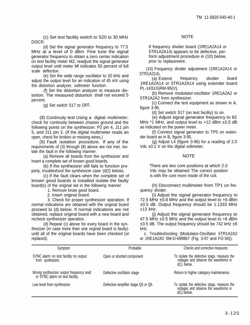
TM 11-5820-540-40-1
(c) Set test facility switch to S20 to 30 MHzDISCR.
(d) Set the signal generator frequency to 77.5MHz at a level of 0 dBm. Fine tune the signalgenerator frequency to obtain a zero center indicationon test facility meter M2; readjust the signal generatoroutput level until meter Ml indicates 50 percent of fullscale deflection.
(e) Set the wide range oscillator to 20 kHz andadjust the output level for an indication of 45 mV usingthe distortion analyzer, voltmeter function.
(f) Set the distortion analyzer to measure dis-tortion. The measured distortionpercent.
(g) Set switch S17 to OFF.
(8) Continuity test Using a
shall not exceed 5
digital multimeter,check for continuity between chassis ground and thefollowing points on the synthesizer: P2 pin 4, J11 pin5, and J11 pin 2. (If the digital multirneter reads anopen, check for broken or missing wires.)
(9) Fault isolation procedure. If any of therequirements of (3) through (8) above are not met, iso-late the fault in the following manner.
(a) Remove all boards from the synthesizer andinsert a complete set of known good boards.
(b) If the synthesizer still fails to function pro-perly, troubleshoot the synthesizer case (d(2) below).
(c) If the fault clears when the complete set ofknown good boards is installed isolate the faultyboard(s) of the original set in the following manner
1. Remove know good board.2. Insert original board.3. Check for proper synthesizer operation. If
normal indications are obtained with the original boardproceed to (d) below. If normal indications are notobtained, replace original board with a new board andrecheck synthesizer operation.
(d) Repeat (c) above for every board in the syn-thesizer (in case more than one orginal board is faulty)until all of the original boards have been checked (orreplaced).
NOTE
If frequency divider board (1RE1A2A14 or5TR1A2A14) appears to be defective, per-form adjustment procedure in (10) below,prior to replacement.
(10) Frequency divider adjustment (1RE1A2A14 or5TR1A214).
(a) Extend frequency divider board1RE1A2A14 or 5TR1A2A14 using extender boardPL-1431/GRM-95(V).
(b) Remove modulator-oscillator 1RE1A2A2 or5TR1A2A2 from synthesizer.
(c) Connect the test equipment as shown in A,figure 3-95.
(d) Set switch S17 (on test facility) to on.(e) Adjust signal generator frequency to 82
MHz *1 MHz, and output level to +12 dBm ±0.5 dBas indicated on the power meter.
(f) Connect signal generator to TP5 on exten-der board as in B, figure 3-95.
(g) Adjust L4 (figure 3-96) for a reading of 2.0Vdc ±0.1 V on the digital voltmeter.
NOTE
There are two core positions at which 2.0Vdc may be obtained The correct positionis with the core more inside of the coil.
(h) Disconnect multimeter from TP1 on fre-quency divider.
(i) Adjust the signal generator frequency to72.5 MHz ±0.8 MHz and the output level to +6 dBm±0.5 dB. Output frequency should be 1.1333 MHz±13 kHz.
(j) Adjust the signal generator frequency to47.5 MHz ±0.5 MHz and the output level to +6 dBm±0.5 dB. The output frequency should be 742 kHz ±8kHz.
c. Troubleshooting (Modulator-Oscillator 5TR1A2A2or 1RE1A2A2 SM-D-698867 (Fig. 3-97 and FO-56)).
Symptom Probable Checks and corrective measures
SYNC alarm on test facility no output Open or shorted component To isolate the defective stage, measure thefrom synthesizer. voltages and observe the waveforms in
d(1) below.
Wrong synthesizer output frequency and/ Defective oscillator stage Return to higher category maintenance.or SYNC alarm on test facility.
Low level from synthesizer Defective amplifier stage Q5 or Q6. To isolate the defective stage, measure thevoltages and observe the waveforms ind(1) below.
3 - 1 2 5

TM 11-5820-540-40-1
Figure 3-95. Frequency Divider 1RE1A2A14 or 5TR1A2A14 Operating Voltage Adjustment Test Setup.
d. Typical Voltage Measurements.(1) Modulator-oscdlator 1RE1A2A2 o r
5TR1A2A2, SM-D-698867 (fig. 3-97).(a) Typical dc voltage indications using the
allocated digital voltmeter and test facility switch S18set at 47.50:
NOTE
Repair or replacement of Q1, Q2, Q3 or
Test points
Q4 emitterQ4 baseQ4 collectorQ5 emitterQ5 baseQ5 collectorQ6 emitterQ6 baseQ6 collector
Typical indications(volts dc)
5.746.22
12.04.04.1
12.04.04.1
12.0their related circuit components will requirerealinement of the modulator-oscillator. (b) Typical signal voltage indications using theRefer to higher catagory maintenance for allocated oscilloscope and test facility switch S18 setrepair. to 47.50.
3-126

TM 11-5820-540-40-1
Figure 3-96. Frequency Divider 1RE1A2A14 or 5TR1A2A14, Parts Location
Typical indications(m V ac p-p)
260250350
1300
3-23. Alarm Control 5TR1A3a. Test Equipment and Material Required
Equipment Common name
Test Facility, Transmitter Transmitter test facilityTS-2866(V)2/GRM-95(V)2
Accessory Kit, Test Facilities Set, Accessory kitMK-1173(V)2/GRM-95(V)2
Multimeter, Digital AN/USM-451 Digital multimeter
b. Test Procedure.(1) Connect the test equipment as shown in figure
3-99, but do not connect the unit under test to the testfacility.
(2) Set the digital multimeter to the 2-volt scale.Set test facility switches S1 and S25 to their ONpositions.
(3) Adjust the test facility SET INPUT control togive a 0.5 V (500 mV) indication on the digitalmultimeter.
Test points
Q4 baseQ5 baseQ6 baseQ6 collectorTP7(+) and TP3(–) of extender board 850
(2) Interconnecting box 1RE1A2A11 or5TR1A2A11 (fig 3-98). Remove all plug-in circuitboards and set test facility switch S17 to ON. Checkthe voltages between the following test points.
Typical indicationTestpoints (volts dc)
TP1(+) to E14(–) 5E3(+) to E14(–) 28E4(+) to E14(-) 12E25(+) to E14(–) 11.5
3-127

TM 11-5820-540-40-1
Figure 3-97. Modulator-Oscillatior 5TR1A2A2 or 1RE1A2A2, Parts Location SM-D-698867.
(4) Connect the unit under test to the test facility (6) Slowly adjust the SET INPUT control in aat J33 as shown in figure 3-99. The digital multimeter clockwise direction (CW) until the panel alarm lightshould indicate at least 460 mV. extinguishes. The digital multimeter should indicate
NOTEbetween 0.110 and 0.150 volts (110 mV and 150 rev).
(7) If the above conditions are not met, proceed
If unable to adequately mate connector J1of UUT and cable assembly CX-12030/Utemporarily remove 2 each stand offs fromconnector J 1 and replace with 2 each 4 X40 binding head screws.
(5) Slowly adjust the SET INPUT control in acounter clockwise direction (CCW) until the panelalarm lamp lights. The digital multimeter should indi-cate 0.080 ±0.005 volts (80 mV ±5 mV).
as follows:(a) Disconnect the unit under test from the test
facility. Adjust the SET INPUT control to obtain a 0.5V (500 mv) indication on the digital multimeter.
(b) On the unit under test, turn the ALARMSENS preset adjust, R7 (figure 3-100) potentiometerCCW for more than 22 turns.
(c) Connect the unit under test to J33 of thetest facility. The digital multimeter should indicate atleast 0.46 V (460 mV).
3-128

TM 11-5820-540-40-1
Figure 3-98. Interconnecting Box 1RE1A2A11 or 5TR1A2A11.
3-129

TM 11-5820-540-40-1
Figure 3-100. Alarm Control 5 TR1A3, Cover Removed.
(d) Slowly adjust the SET INPUT controlCCW until the panel alarm lamp lights. The digitalmultimeter should indicate more than 0.16 V (160mv).
(e) On the unit under test, turn the ALARMSENS adjust (R7) potentiometer CW for more than 22turns. Reset the SET INPUT control to obtain a 0.5 V(500 rev’) indication on the digital multimeter.
(f) Slowy adjust the SET INPUT control CCWuntil the panel alarm lamp lights. The digital mul-timeter should indicate less than 0.075 V (75 rev).Turn the SET INPUT control CW until the alarm lampextinguishes.
(g) Adjust the SET INPUT control to obtain anindication of 0.080 V (80 mv) on the digital mul-timeter. On the unit under test, adjust turn ALARMSENS adjust (R) potentiometer until the alarm lamplights.
(h.. Adjust the SET INPUT control to obtain a0.5 V (500 mV) indication on the digital multimeter,
then slowly turn the control CCW until the alarm lamplights. The multimeter should indicate 0.080 ±0.005 V(80 ±5 rev).
(i) Repeat procedures (1) through (7) above.
C. Troubleshooting (fig. 3-101).
Check and correctiveSymptom measures
Incorrect meter reading; Measure the voltage at CR2,Test facility control alarm CR3, CR4, Q1, and Q2 (fig.lamp lights. 3-101 and FO-36) as de-
scribed in d below.
Correct meter reading control Measure the voltage at Q3 andalarm lamp lights. Q4 (d. below). Check relay
K1 as described below.Normal indications; but control Check relay K1 contacts for
alarm lamp does not light continuity (between E1 andE2 terminals). Replace ifcontacts are sticking.
3-130

TM 11-5820-540-40-1
Figure 3-101. Alarm Control 5TR1A3A1, Parts Location
3-131

TM 11-5820-540-40-1
3-24. Amplifier-Frequency Multipliera. Test Equipment Required.
Equipment Common name
Test Facility, TransmitterTS-2866(V)2/GRM-95(V)2
Accessory Kit, Test FacilitiesMK-1173(V)2/GRM-95(V)2
Accessory Kit, Test FacilitiesMK-1985(V)2/GRM-95(V)2
Test Facility, ReceiverTS-2867(V)2/GRM-95(V)2
Test Facility, RF ModulesTS-3837(V)2/GRM-95(V)2
Sweep Generator, Wiltron 610DPlug-in Unit Wiltron 61084DPower Meter HP-435APower Sensor HP-8481AOscilloscope AN/USM-281CRf Power Amplifier ENI 603LSignal Generator HP 8640BRf Voltmeter ME-426/UDigital Multimeter AN/USM-451
Transmitter test facility
Accessory kit
Accessory kit
Receiver test facility
Module test facility
Sweep generatorPlug-in unitPower meterPower sensorOscilloscopePower amplifierSignal generatorRf voltmeterDigital multimeter
NOTE
Set power supply PP-6304/GRM-95(V) fora 115 Vac output as indicated on its panelvoltmeter. Maintain this output throughoutthe following procedures.
CAUTION
The attenuators selected for usethroughout this paragraph are to preventaccidental damage to test equipment andto the unit under test. Extreme cautionmust be exercised when theseattenuators are not used.
The rf signal level input to RF INPUT ofthe power amplifier, ENI 603L, must notexceed –5 dBm.
The rf signal level input to RF IN, J39 onthe test facility, must not exceed +20dBm.
Rf output levels at RF OUT, J38 on thetest facility, can exceed 6 W (+37.8dBm), and 3 W (+34.8 dBm) at RF OUTon the power amplfler. These outputsmust be connected to 50 ohm loads at alltimes and caution must be exercised toavoid damage to any equipment connect-ed to these outputs.
b. Test Procedures.(1) Input VSWR Test
(a) Connect the equipment as shown in A,figure 3-102.
(b) Set the sweep generator controls for a CWoutput at a frequency of approximately 60 MHz.Adjust the rf output level for a +10 dBm indication onthe power meter.
(c) Connect the equipment as shown in B,figure 3-102.
(d) Set the sweep generator controls for asweep output from 47.5 MHz to 72.5 MHz, and adjustthe oscilloscope controls for a convenient display withat least a 4 cm vertical displacement. This is the 2:1VSWR reference. Note this reference and do not read-just the sweep generator output or oscilloscope verti-cal controls.
(e) Connect the equipment as shown in C,figure 3-102. Turn test facility switches S1 to ON, S20to S30, and S30 to ON.
(f) The VSWR as displayed on the oscilloscopeshall be less than the 2:1 reference from 47.5 to 72.5MHz.
(g) Turn S30 to OFF.(2) Power output check.
(a) Remove the chassis cover opposite P1 ofthe unit under test and connect the equipment asshown in A, figure 3-103.
(b) Set the test facility switches as follows:
Switch Position
S12 ONS1 ONS20 S30S30 ON
(c) Adjust the signal generator for an outputlevel of +15 dBm as indicated on the power meter at afrequency of 47.5 MHz.
(d) Connect the equipment as shown in B,figure 3-103. The power output of the unit under testshould be not less than +34 dBm (+14 dBm powermeter indication), test facility meter Ml indicationshould be not more than 75% and the digital mul-timeter should indicate not more than 0.450 Vdc.
(e) Slowly vary the signal generator frequencyfrom 47.5 MHz to 72.5 MHz. The power output, Mland digital multimeter indications should remain asspecified in (d) above.
(f) Repeat (a) and (c) through (e) above for a signal generator output level of +12.5 dBm. Thepower output and Ml indication should remain asspecified in (d) above and the digital multimetershould indicate not less than 175 m Vdc.
3-132

TM 11-5820-540-40-1
Figure 3-102. Amplifier-Frequency Multiplier 5TR1A4 VSWR Test Setup.
3-133

TM 11-5820-540-40-1
(g) Set the signal
Figure 3-103. Amplifier-Frequency Multiplier 5TR1A4 Power Output, Test Setup.
generator RF switch to OFF. (l) Set test facility switch S30 to AGC 3. TheTest facility meter M1 should indicate not more than power meter indication should decrease further to at20%. Reset the RF switch to ON.
(h) If an unstable output is obtained, realinethe unit under test as described in the alinement pro-cedure (para. e).
(i) Set the signal generator frequency to 47.5MHz. Note the power meter indication.
(j) Set test facility switch S30 to AGC 1. Thepower meter indication should not decrease more than1 dB below the indication noted in (i) above.
(k) Set test facility switch S30 to AGC 2. Thepower meter may indicate a decrease in power.
least 3 dB below the indication noted in (i) above.(m) Repeat (i) through (l) above at 60 MHz and
72.5 MHz.(n) Replace the cover on the unit under test.
(3) Harmonic and fundamental frequency rejectiontest.
(a) Connect the equipment as shown in figure3-104 using the 95 to 190 MHz filter, and set testfacility switch S30 to ON.
3-134

TM 11-5820-540-40-1
(b) Set the signal generator to 47.5MHz andadjust the OUTPUT LEVEL control for an output of+12.5 dBm.
(c) Adjust the filter around 142.5 MHz for apeak indication on the rf voltmeter. This is the thirdharmonic of the unit under test input frequency. Thepeak rf voltmeter indication should not exceed – 17dBm.
(d) Tune the signal generator from 47.5 to 72.5MHz while maintaining a peak indication on the rfvoltmeter by tracking the filter to the third harmonic ofthe signal generator frequency (142.5 to 217.5 MHzfilter frequency).
CAUTION
Figure 3-104. Amplifier-Frequency Multiplier 5TR1A4, Harmonic Rejection Test Setup.
Turn test facility switch S30 to OFF whenchanging filters.
NOTE
For third harmonic frequencies above 190MHz (63.3 MHz signal generator fre-quency) change to the 190 to 400 MHzfilter.
(e) The rf voltmeter peak indication should notexceed – 17 dBm.
(f) Set the signal generator to 48.5 MHz andtune the 190 to 400 MHz filter around 194 MHz for apeak rf voltmeter indication of the fourth harmonic.The rf voltmeter peak indication shall not exceed – 12dBm.
(g) Repeat (b) through (d) above using the 48 to95 MHz filter tuned to the fundamental (input) fre-quencies from 48.3 to 72.5 MHz. The rf voltmeterpeak indication shall not exceed –17.5 dBm.
(h) Turn test facility switch S30 to OFF.
3-135

TM 11-5820-540-40-1
c. Troubleshooting (F0-23).
Symptom Checks and corrective measures
1. No output (para. b a. Check +28 Vdc supply at L10,(2) above). L12, and L16; investigate any
abnormal indication; replacecomponents as required (fig.3-105).
b. Using oscilloscope, check the inputsignal at E1 and E3(5TR1A4FL1); refer to chartd(l) below. If signal not presentat E3, check continuity of L1through L4 (5TR1A4FL1).If defective, replace5TR1A4FL1 (fig. 3-106).
c. Check connector and cable Al ofP1 to E1 (5TR1A4FL1), repairor replace cable and connector.
d. If signal normal at E3(5TR1A4FL1), check signalthrough transistor stages (chartd(1) below). If signal at Q1 isabnormal, check continuity ofT1 windings, and forward andreverse resistances of CR1diodes.
e. If problem is isolated to transis-tor stage, check voltages and re-sistances. Refer to paragraph dbelow for transistor resistancemeasurements.
f. If transistor stages check normal,check continuity of componentsfrom Q3 through E9 and cablefrom E9 to connector A2 of P1for short circuit. Repair or re-place components as required.
2. Output normal, no Check CR1, mounted between filtersmeter M1 indication. FL4 (maybe marked FL1 on older
units) and FL3, for possible shortcircuit, and L 17 and R 17 for opencircuit; replace components asrequired.
3. Excessive currentconsumption.
Check R1 and R2 for open circuit;resolder connections if loose.
Symptom Checks and corrective measures
4. Low output a. Using oscilloscope, check gainof transistor stages. Refer tochart d(1) below. Checkcomponents in isolated stageand replace as required.
b. Check continuity of com-ponents from Q3 through A2of P1. Replace or repairas required.
c. Check alinement and frequencyresponse. Refer to paragraphe below.
5. High VSWR level (b Check input filter components; refer(1) above) to fig.3-106.
6. High harmonic level Check alinement; refer to(b(3) above) e(2) below
d. Signal Voltage and Resistance Measurements.(1) Signal voltages (Fig. 3-107).
Test points Typical indication
E1E3Q1-Base
-CollectorQ2-Base
-CollectorQ3-Base
-Collector
3.0 V peak-to-peak3.0 V peak-to-peak250 mV peak-to-peak875 mV peak-to-peak750 mV peak-to-peak4.0 V peak-to-peak2.5 V peak-to-peak4.0 V peak-to-peak
NOTE
The value of resistor R12 is selected undertest. If Q3 is replaced and the outputremains low, change R12 from 56 ohms to150 ohms or vice versa.
(2) Transistor resistance measurenments.
NOTE
All resistances measured with the allocateddigital multimeter.
3-136

Figure 3-105
Figure 3-106.
TM 11-5820-540-40-1
3-137

Figure 3-108.
TM 11-5820-540-40-1
Figure 3-107. Amplifier-Frequency Multiplier 5TR1A4, Parts Location
3-138

TM 11-5820-540-40-1
(e) Note the vertical deflection level displayedfor 60 MHz. This is the minimum output power level(+34 dBm) reference line (disregard deflection levelvariations at other frequencies). Do not readjust theoscilloscope vertical controls without repeating (a)through (e) above.
(f) Connect the equipment as shown in C, figure3-108.
(g) Set the step attenuators for 2.5 dB.(h) Set the sweep generator for a 60 MHz CW
power meter indication of –7.5 dBm (equivalent to+12.5 dBm to be delivered to the unit under test).
(i) Return the sweep generator to sweep mode.(2) Response.
(a) Remove the chassis covers from the unitunder test. Remove the protective caps from the tun-ing capacitors.
(b) Set the controls on the unit under test aslisted below (refer to figure 3-107 for controllocations).
Control Setting
C-31 Fully counterclockwise (min. capacitance)c-35 Fully clockwise (max. capacitance)C-36 Fully clockwise (max. capacitance)C-14 Midrangec-22 MidrangeC-26 MidrangeC-27 MidrangeR-1 FulIy counterclockwise (min. resistance)R-2 Fully counterclockwise (min. resistance)
NOTE
1. C-31 is kept at its minimum capacitance.2. C-35 affects the high
point.3. C-36 affects the low
point and notch frequency.4. C-14 and C-22 affect
amplitude.5. C-26 and C-27 affect
response.
frequency cut-off
frequency cut-off
response tilt and
the center of the
6. R-1 and R-2 affect the depth of the notchand harmonic rejection.
7. Use internal or external sweep generatormarkers to identify frequencies of interest.
(c,) Connect the equipment, calibrated as in (1)above, to the unit under test as shown in figure 3-109.
(d) Set the test facility switches as follows:
Switch Position
S1 ONS30 ONS20 S30
(e) Adjust C-35 on the unit under test for amaximum amplitude response at 72.5 MHz. Do notadjust C-35 to its minimum capacitance position.
(f) Adjust C-14, C-22, C-26, C-27, C-35 and C-36 for a flat response similar to the response shown infigure 3-110 with the notch adjusted (C-36) to approx-imately 45 MHz and the response from 47.5 to 72.5MHz displayed above the reference line noted in (1)(e)above.
(g) Adjust R1 and R2 for a minimum amplituderesponse at the notch. Keep R1 and R2 as close tominimum resistance as possible.
(h) Repeat (e) and (f) above, as necessay, untilthe requirements of (f) above are met.
(i) Set the step attenuators for O dB and thesweep generator for manual sweep operation.
(j) Using the MANUAL control, slowly tune thesweep generator from 47.5 MHz to 72.5 MHz whileobserving test facility meter Ml indication. Meter Mlindication should not exceed 7 5‘% through the tuningrange. If necessary, repeat (c), (f) and (h) through (j)above until the requirements of (f) and (j) are met(adjust C14 to increase output level or decrease M1indication).
NOTE
R12 is to be selected as required to meetthe requirements of (f) and (j) above andmay be either 50 ohms or
(k) Set transmitter testpower amplifier switch to OFF.
(3) Harmonic rejection.
150 ohms ±5%.
facility switch S30 and
NOTE
while performingIf adjustments are madethe following checks, repeat the tests (andadjustments) in paragraph (2)(c) through(k)until all requirements are met.
(a) Connect the equipment as shown in figure3-104 using the 95 to 190 MHz filter.
(b) Set test facility switch S30 to ON.(c) Set the signal generator for 47.5 MHz at
+12.5 dBm output.(d) Adjust the filter around 142.5 MHz for a
peak indication on the rf voltmeter of the third har-monic of the input frequency. The rf voltmeter indica-tion should not exceed – 17 dBm.
(e) If necessary, adjust R1 and R2 on the unitunder test for a minimum rf voltmeter indication. KeepR1 and R2 adjusted as close to minimum resistance aspossible.
3-139

TM 11-5820-540-40-1
Figure 3-108. Amplifier-Frequency Multiplier 5TR1A4, Power Output Test Setup Calibration.
3-140

TM 11-5820-540-40-1
Figure 3-109. Amplifier-Frequency Multiplier 5TR1A4, Power Output Response, Test Setup.
3-141
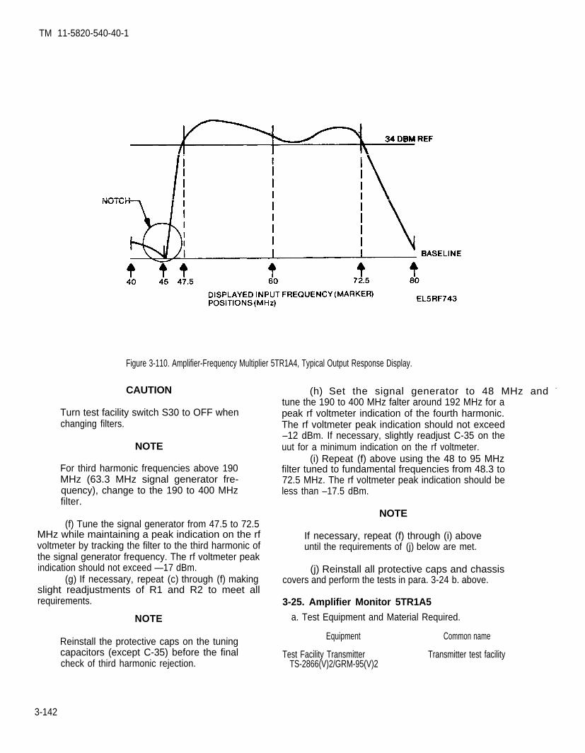
TM 11-5820-540-40-1
Figure 3-110. Amplifier-Frequency Multiplier 5TR1A4, Typical Output Response Display.
CAUTION
Turn test facility switch S30 to OFF whenchanging filters.
NOTE
For third harmonic frequencies above 190MHz (63.3 MHz signal generator fre-quency), change to the 190 to 400 MHzfilter.
(f) Tune the signal generator from 47.5 to 72.5MHz while maintaining a peak indication on the rfvoltmeter by tracking the filter to the third harmonic ofthe signal generator frequency. The rf voltmeter peakindication should not exceed —17 dBm.
(g) If necessary, repeat (c) through (f) makingslight readjustments of R1 and R2 to meet allrequirements.
NOTE
Reinstall the protective caps on the tuningcapacitors (except C-35) before the finalcheck of third harmonic rejection.
(h) Set the signal generator to 48 MHz and -
tune the 190 to 400 MHz falter around 192 MHz for apeak rf voltmeter indication of the fourth harmonic.The rf voltmeter peak indication should not exceed–12 dBm. If necessary, slightly readjust C-35 on theuut for a minimum indication on the rf voltmeter.
(i) Repeat (f) above using the 48 to 95 MHzfilter tuned to fundamental frequencies from 48.3 to72.5 MHz. The rf voltmeter peak indication should beless than –17.5 dBm.
NOTE
If necessary, repeat (f) through (i) aboveuntil the requirements of (j) below are met.
(j) Reinstall all protective caps and chassiscovers and perform the tests in para. 3-24 b. above.
3-25. Amplifier Monitor 5TR1A5
a. Test Equipment and Material Required.
Equipment Common name
Test Facility Transmitter Transmitter test facilityTS-2866(V)2/GRM-95(V)2
3-142

TM 11-5820-540-40-1
Equipment
Accessory Kit, Test Facilities SetMK-1173(V)2/GRM-95(V)2
Voltmeter, Elecronic ME-459/UGenerator, Signal AN/USM-205A
Figure 3-111. Amplifier-Monitor 5TR1A5, Test Setup.
Common name b. Test Procedure.(1) Order wire terminating resistor.
Accessory kit (a) Set multimter to 2k ohm scale.
Multimeter, Digital AN/USM-451Oscilloscope AN/USM-281CElectronic Counter TD-1225(V)1/U
(b) Meausre resistance between pins 3 and 16VTVM of connector P 1 on unit under test. Resistance shouldWide range be 620 ohms ±5%.
oscilloscopeDigital Multimeter (2) Amplifier gain test.Oscilloscope (a) Connect the test equipment as shown inFrequency counter figure 3-111.
3-143

TM 11-5820-540-40-1
Figure 3-112. Video Amplifier 5TR1A4AR1, Parts Location
Figure 3-113. Video Monitor 5TR1A5A1, Parts Location.
3-144

TM 11-5820-540-40-1
(b) Set the test facility switches as follows:
Switch Position
S1 ONS20 S28S28 OWS29 INPUT
(c) Adjust the wide range oscillator to 10 kHz at246 mV (– 10 dBm) as shown on the VTVM.
(d) Set test facility switch S29 to OUTPUT.The VTVM should indicate 32 mV ±1 mV.
(e) If necessary adjust R26 (fig. 3-112) toobtain the value given in (d) above.
(3) Relays and attenuator operation.(a) Using the test setup shown in figure 3-111,
set test facility switch S28 to 0 dB and S29 toOUTPUT.
(b) Adjust the wide range oscillator output con-trol to obtain a – 10dB indication on the VTVM.
(c) Set test facility switch S28 to 3.5 dB. TheVTVM should indicate – 13.5 dB ±0.3 dB.
(d) Set switch S28 to 6.0 dB. The VTVMshould indicate – 16 dB ±0.3 dB.
(e) Set switch S28 to 12.0 dB. The VTVMshould indicate –22 dB ±0.3 dB.
(4) Metering circuits.(a) Using the test setup shown in figure 3-111
set test facility switches S28 to FDM and S29 toOUTPUT.
(b) Adjust the output of the wide rangeoscillator until the VTVM indicates 53 mV. Testfacility meter M1 should indicate 50 percent of fullscale deflection.
(c) If necessary, on the unit under test, adjustR12 (fig. 3-113) to obtain the indication given in (b)above.
(d) On the test facility, set switch S28 to 12CHAN. Adjust the wide range oscillator output for a128 mV indication on the VTVM. Meter Ml shouldindicate 50 percent of full scale deflection.
(e) If necessary, on the unit under test, adjustR11 (fig. 3-113) to obtain the indication given in (d)above.
(f) Set test facility switch S28 to 24 CHAN.Adjust the wide range oscillator output for a 212-mVindication on the VTVM. Meter M1 should indicate 50percent of full scale deflection.
(g) If necessary, on the unit under test, adjustR10 (fig. 3-113) to obtain the indication given in (f)above.
(5) Frequency response.(a) Using the test setup shown in figure 3-111,
set test facility switches S28 to 24 CHAN and S29 toINPUT.
(b) Set the test oscillator frequency to 10 kHzas indicated on the electronic counter.
(c) Adjust the amplitude control on the testoscillator to obtain a – 10 dB indication on the VTVM.
(d) Set switch S19 to OUTPUT. The VTVMshould indicate –10 dB ±1.0 dB. Note the exactindication obtained.
(e) Set switch S29 to INPUT. Set the testoscillator frequency to 283 kHz as indicated on theelectronic counter. Adjust the amplitude control on thetest oscillator as required to obtain a – 10 dB indica-tion on the VTVM.
(f) Set switch S29 to OUTPUT. The VTVMshould indicate 0.75 dB ±0.2 dB below the indicationobtained at 10 kHz in (d) above.
(g) Repeat steps (e) and (f) above for theremaining test frequencies listed in the table below.
Output voltage relativeto output voltage amplitude
Test frequencies (kHz) at 10 kHz (dB)
283 –0.75 ±0.2567 –3.00 ±0.2850 –6.75 ±0.3960 –8.60 ±0.6
C. Troubleshooting (FO-24),
Symptom Checks and corrective measures
No output (b(2)(e) above). Check operating voltages oftransistor stages on printedcircuit board5TR1A5AR1 (d below).Replace defective componentsas required
Low output (b(2)(e) above). a. Measure the signal voltage be-tween E9 and E1O(5 TR1A5AR1), figure 3-112,with the AC voltmeter while10 kHz at –10 dB is presentat input; level should be490 mVrms ±10 mV. If levelat E 10 is normal, checkoperation of attenuatorrelay K1, K2 and K3. Replacerelays as necessary.
b. Vary R26; if output does notchange, check continuity offeedback circuit R26, R13and C4 (5 TR1A5AR1).
c. Check C5 (5 TR1A5AR1 ) foropen circuit replace ifnecessary.
Normal output; abnormal a. Measure the voltages and re-indications with switch sistances of Q1 and Q2 (fig.S28 set to FDM, 12 CHAN 3-113). 5TR1A5A1 (d below).or 24 CHAN positions Replace component as(b(4) above). required.
3-145

TM 11-5820-540-40-1
Symptom Checks and correction measures 3-26. Power Supply 5TR1PS1b. Check the forward and reverse
resistances of diodes CR 1,CR2 and CR3. Replace asrequired.
Output distorted (b(5)(g) Using the oscilloscope, observeabove). the output of transistor stages
Q1, Q2 and Q3 (5TRA5AR1).Check the voltage and resis-tances of isolated stage.Replace component as required
Abnormal output indication Check input signal through FL1with switch S28 set to (5 TR1A5AR1); replace FL1 ifFDM (b(4)(b) above). necessary.
d. Voltage and Resistance Measurements.
NOTEWARNING
All voltages and resistances measured withthe allocated digital multimeter.
(1) In-circuit voltage measurements.Typical indication
Test points (Vdc)Video Amplifier 5TR1A5AR1:
Q1-Emitter +1.4-Base +2.1-Collector +6.0
Q2-Emitter +1.6-Base +2.3-Collector +6.0
Q3-Emitter +5.3-Base +6.0-Collector +12.0
Video Monitor 5TR1A5A1:Q1-Emitter +1.6
-Base +2.3-Collector +10.0
Q2-Emitter +9.5-Base +10.0-Collector +28.0
(2) Resistance measurements.
a. Test Equipment and Material Required.
Equipment Common name
Test Facility, TransmitterTS-2866(V)2/GRM-95(V)2
Accessory Kit, Test Facilities SetMK-1173(V)2/GRM-95(V)2
Test Facility, RF Modules,TS-3837(V)2/GRM-95(V)2
Oscilloscope AN/USM--281CMultimeter, Digital AN/USM-451Counter, Electronic, Digital Read-
out TD-1225(V)1/U
b. Test Procedure.
Transmitter test facility
Accessory kit
Test facility, rfmodules
OscilloscopeMultimeterCounter
High voltages are present on the unit undertest. Always switch test facility switch S2 toOFF when connecting probes.
(1) Input rectification circuit check.(a) Connect the test equipment as shown in
figure 3-114.(b) Place the unit under test in front of the air
outlet so that the airflow will be directed over the heatsink.
(c) Connect the positive lead of the multimeterto C1 (+) and the negative lead to C1 (–).
(d) Set test facility switches S1 and S2 to theirON positions. The test facility blower fan shouldoperate.
(e) Check the voltage on the power supply (partof the accessory kit); if necessary adjust for 115 Vat.The multimeter connected to Cl should indicate 103 V±5V.
(f) Set switch S2 to OFF and disconnect themultimeter leads from C1.
3-146

TM 11-5820-540-40-1
Figure 3-114. Power Supply 5TR1PS1, Inverter Circuits Checks, Test Setup.
(2) Rise time and frequency measurement. INVERT. Select 10 V scale on each channel and usetwo 10x probes. Connect the probes to pins 1 and 3 of
(a) Using the test setup shown in figure 3-114, T2.locate transformer T2 (fig. 3-115) on the unit under (b) Press and hold test facility switches S3, S5test. Set the oscilloscope MODE selector to ADD and and S7, then switch S2 to ON. The oscilloscope shouldRIGHT vertical channel POLARITY switch to indicate 5 kHz ±1 kHz.
3-147

TM 11-5820-540-40-1
Figure 3-115. Power Supply 5TR1PS1, with Heat Sink Removed.
3-148

TM 11-5820-540-40-1
(c) Set test facility switch S4 to 600 V. The risetime (10 percent to 90 percent of peak-to-peakamplitude) measured on the oscilloscope should beless than 2.5 microseconds. Set switch S2 to OFF.
(d) Connect the oscilloscope probes to pins 4and 6 of transformer T1.
(e) Connect the counter to pins 11 and 12 oftransformer T1. Pin 12 should be the ground side ofthe counter.
(f) Set switch S2 to ON. Push and hold S3, S5and S7. The counter should indicate 400 Hz ±40 Hz.The rise times are as follows:
1. From 10% to 90% of peak-to-peak, lessthan 15 microseconds.
2. From 20% to 90% of peak-to-peak, lessthan 5 microseconds.
(g) Set switch S2 to OFF. Disconnect theoscilloscope and the counter.
(3) Load and voltage regulation check.(a) Using the test setup shown in figure 3-114,
connect the multimeter to connectors J2 and J6 on thetest facility. Set S4 to +12 V, S20 to S4 and set switchS2 to ON. The multimeter should indicate between12.0 volts and 12.5 volts.
(b) Press switches S5 and S7. The multimetershould indicate between 11.8 volts and 12.2 volts.Record this indication. Note test facility meter M 1indication and set S4 to +12 V METER position. Testfacility meter Ml indication should be the same as pre-viously noted, ± the width of the pointer.
(c) Keeping switches S5 and S7 pressed, slowlyvary the voltage control on the power supply between105 Vac and 125 Vac. The multimeter indicationshould not change by more than 0.2 V from(b) above.
(d) Release switch S5 and S7 and reset thevoltage control to 115 Vac.
(e) Connect multimeter to connectors J2 andJ12 on the test facility. Set switch S4 to +28 V posi-tion. Press switches S5 and S7; multimeter shouldindicate between 28.1 volts and 28.5 volts. Record themultimeter indication. Note test facility meter M 1indication and set test facility switch S4 to +28 VMETER position. Test facility meter Ml indicationshould be the same as previously noted ± the width ofthe pointer.
(f) Slowly vary the power supply voltage controlbetween 105 Vac and 125 Vat. The multimeter indica-tion should not change by more than 0.2 V from thereading obtained in (e) above.
(g) Release switches S5 and S7 and reset thevoltage control to 115 Vat, and disconnect themultimeter.
(4) Short Circuit protection check.
(a) Using the test setup shown in figure 3-114,set test facility switch S4 to +12 V and switch S2 toON. Note the indication on test facility meter Ml. Setswitch S2 to OFF.
(b) Connect the multimeter (set to 10A DC fullscale) to test facility connectors J2 and J6 as shown infigure 3-116.
(c) Set switch S2 to ON; the multimeter shouldindicate 2.2 amp ±0.4 amp.
(d) Set switch S2 to OFF. Remove the mul-timeter leads from connectors J2 and J6.
(e) Set switch S2 to ON; meter M1 should indi-cate the same as in(a) above.
(f) Set switch S4 to +28 V; note the indicationon meter Ml.
(g) Set switch S2 to OFF. Connect the mul-timeter to connectors J2 and J12 on the test facility.
(h) Set switch S2 to ON; the multimeter shouldindicate 2.5 amp ±0.5 amp.
(i) Set switch S2 to OFF. Remove the leadsfrom connectors J2 and J12 on the test facility.
(j) Set switch S2 to ON; meter M1 should indi-cate the same as noted in (f) above.
(5) Filament supply check.(a) Remove the red plastic warning cover from
the filter section for the unit under test.(b) Connect the multimeter to FL21 (+) and
FL20(–) (output filament) (figure 3-115).(c) Set multimeter range to 20 Vdc.(d) Set S2 to ON and press S3, S5 and S7. The
multimeter should indicate 8.2 Vdc ±0.8 V. Set S2 toOFF.
(e) Repeat (a) through (c) above with mul-timeter connected to FL23(+) and FL22 (–) (driverfilament). The multimeter should indicate 8.2 Vdc±0.8 V.
(f) Set S2 to OFF.(6) Constant current check.
(a) Using the test setup shown in figure 3-114,set test facility switch S4 to DRIVER CUR. Testfacility meter M1 should indicate in the green band.
(b) Turn the power supply voltage control to 70Vac as indicated on the power supply panel. Ml shouldindicate in the green band. Reset the voltage control to115 Vat.
(c) Set switch S4 to OUTPUT CUR. Meter M1should indicate in the green band.
(d) Turn the power supply voltage control to 70Vac as indicated on the power supply panel. Meter M1should indicate in the green band. Reset the voltagecontrol to 115 Vac and set switch S2 to OFF.
(7) 26 volt unregulated supply check.(a) Set the multimeter to the 200 volt range
and connect to J2 (–) and J9 (+).
3-149

TM 11-5820-540-40-1
Figure 3-116. Power Supply 5TR1PS1, Short Circuit Protection and Hum Checks, Test Setup.
(b) Set S4 to 26 volts.(c) Press S3, S5 and S7.(d) Ensure that the ac voltmeter on power sup-
ply PP-6304 is indicating a supply voltage of 115 Vat.The multimeter should indicate 26.5 V ±1.5 V andmeter M1 should indicate between 4570 and 5570.
(e) Set S2 to OFF.(8) 600 V output and meter circuit check.
(a) Using the test setup shown in figure 3-114,connect the multimeter negative lead to ground andthe positive lead to FL24 (fig. 3-115).
(b) Set switch S4 to 600 V METER position.Press and hold switch S3. Set switch S2 to ON.
(c) Adjust the voltage control on the PP 6304power supply to give an indication of 630 Vdc ±1 V onthe multimeter.
(d) On the unit under test adjust R18 control(fig. 3-117) for an indication of 50 percent of full scaleon test facility meter M1.
(e) Release switch S3 and set switch S2 to OFF.Remove the multimeter connections. Reset the voltagecontrol to 115 Vat.
(f) Seal R18 as described in paragraph 2-12.(g) Set S4 to 600 volts.(h) Press load switch S3.(i) Meter M1 should indicate between 45% and
55%.(9) Hum measurements. Using the test setup
shown in A, figure 3-116, connect the VTVM to J1 onthe transmitter test facility. Set test facility switch S4to the positions listed below and measure the ripplevoltage.
3-150

TM 11-5820-540-40-1
Figure 3-117. Power Supply 5TR1PS1, Showing Access to Power Supply Subassembly 5TR1PS1A1.
Secondary Ripple indicatedS4 position action by VTVM
+12V Press S5 and S7 Less than 3.5 mV+26 V Press S3, S5 and S7 Less than 350 mV+28 V Press S5 and S7 Less than 3.5 mV
OUTPUT FIL Press S3, S5 and S7 Less than 120 mVDRIVER FIL Press S3, S5 and S7 Less than 120 mV
above OUTPUTFIL indication
(10) Blower voltage and low power alarm supplycheck.
(a) Set the multimeter for ac volts and 200 voltrange.
(b) Connect the multimeter to FL5 and FL6(figure 3-1 15).
(c) Set S2 to ON. The multimeter should indi-cate 142 Vac ±8 V.
(d) Set S2 to OFF.(e) Connect the multimeter to FL7 and FL8.(f) Set S2 to ON. The multimeter shouId indi-
cate 30 V ±3 V.(g) Set S2 to OFF.(h) Replace both plastic protective covers.
3-151

TM 11-5820-540-40-1
c. Troubleshooting (FO-25).
Symptom Probable cause Checks and corrective measures
1. Low voltage across C 1, b(1) above.
2. 5 kHz or 400 Hz risetime or frequencyabnormal, b(2) above.
3. +12 V or 28 V checks abnormal, b(3)above.
4.
5.
6.
7.
8.
9.
Abnormal indication, b(4)(c) and (h)above.
Abnormal filament supply voltage,b(5) above.
Meter M1 indication abnormal, b(6)above.
26 volt indication abnormal, b(7) above
600 V supply indications abnormal, b(8)above.
Hum measurement beyond specifiedlimits.
a. Relay K4 inoperative.
b. Defective diodes CR1, CR2, CR3 or CR4on heat sink 5TR1PS1A2 (fig. 3-118).
Defect components, heat sink 5TR1PS1A2or 5TR1PS1 (chassis)
a. +12 V and +28 V regulator5TR1PS1AR1 defective or mis-adjusted.
b. Defective components, heatsink5TR1PS1A2.
c. Defective components, 5TR1PS1(chassis)
Defective diode CR6, CR5, R2 or R1.
Defective power supply 5TR1PS1PS1, T2 orFL29.
Defective transistor Q13 or Q14(5TR1PS1A2)or CR14 or CR15 andassociated circuitry (5TR1PS1A1)
Defective CR6 or L1 and associatedcircuitry.
Relay K2, T3, CR 15 or associated circuitcomponents.
a. +12 V: defective C 17 (5TR1PS1A2)b. +28 V: defective C19 or C9 (5TR1PS1)c. DRIVER HEATER: defective C1
(5TR1PS1PS1)d. OUTPUT HEATER: defective C2
(5TR1PS1PS1)
a. Check for +26 Vdc between FL17 (+) andFL16 (–) (fig. 3-115). If present, checkrelay K4.
b. Check and replace faulty diodes asrequired.
Test per paragraph 3-27 or 3-29 and replacedefective components.
a. Check and adjust 5TR1PS1AR1 asoutlined in paragraph 3-28.
b. Check 5TR1PS1A2 as described in para-graph 3-27.
c. Check 5TR1PS1 (chassis) as describedin paragraph 3-29.
Check and replace components as required.
Test power supply chassis, paragraph 3-29.
Check 5TR1PS1A2, paragraph 3-27 or5TR1PS1A1 (P/O power supply chassis),paragraph 3-29.
Check 5TR1PS1 (chassis), paragraph 3-29.
Check operation of K2. If normal, check5TR1PS1 (chassis), paragraph 3-29.
a. Check or replace C17.b. Check or replace C19 or C9.c. Check or replace C1.
d. Check or replace C2.
3-27. Power Supply Subassembly 5TR1PS1A2
a. Test Equipment and Material Required.
Equipment Common name
Test Facility, Transmitter Transmitter test facilityTS-2866(V)2/GRM-95(V)2
Accessory Kit, Test Facilities Set Accessory kitMK-2867(V)2/GRM-95(V)2Test Facility, RF ModuIes, Test facility, rf modules
TS3837(V)2/GRM-95(V)2Oscilloscope AN/USM-281C OscilloscopeMultimeter, DigitalAN/USM-451 Digital multimeterCounter, Electronic, Digital Readout Counter
TS-1225(V)I/UInsulation Tester GR-1864 Insulation tester
b. Test Procedure.
(1) Remove the larger red protective cover toexpose power supply subassembly (heat sink)5TR1PS1A2.
(2) Remove 5TR1PS1A2 by loosening the twogreen-circled mounting screws and pulling the modulestraight up.
(3) Open the test facility power supply door.Remove jumper cables between J4-J5 and J10-J11.Connect 5TR1PS1A2 and the test facility as shown infigure 3-119.
(4) Place the unit under test in front of the airoutlet so that the airflow is directed over the heat sink.
3-152

TM 11-5820-540-40-1
Figure 3-118. Power Supply Subassembly 5TR1PS1A2, Parts Location
WARNING
The outer cases of the transistors mountedon the heat sink are connected to highvoltage.
NOTE
Throughout the following tests, maintainthe input voltage at 115 Vac as shown onthe power supply voltmeter (part of theaccessory kit).
(5) Set the test facility switches as follows:
Normal M1Switch Switch position Secondary action indication
S1 ONS20 S4S2 ON54 +12V METER Press S5 and S7. 40% to 60%S4 +28V METER Press S7 and S5. 45% to 55%54 +26V Press S3, S5 and S7. 45% to 55%54 DRIVER FIL Press S3, S5 and S7. 50% to 70%S4 OUTPUT FIL Press S3, S5 and S7. 50% to 70%S4 DRIVER CUR Green band.54 OUTPUT CUR Green band.
Normal MlSwitch Switch position Secondary action indication
S4 600V S2 to OFF. 45% to 55%Press and holdswitch S3 thenset switch S2to ON.
S4 26 VAC Green band.(6) Set S4 to +26 V. Operate S2 to ON and OFF
three times fairly quickly. M1 should indicate withinthe green band each time S2 is switched to ON. Thischecks the starting circuit.
(7) Check input rectification circuit as follows:(a) Connect the digital multimeter across
capacitor Cl 8 (observe polarity) as shown in figure 3-119.
(b) Set S2 to ON.(c) The digital multimeter should indicate 100
V ±5 V.(d) Set S2 to OFF.
(8) 5 kHz inverter check.(a) Connect the oscilloscope 10x probes to ter-
minals E8 and E11 on the unit under test.(b) Set oscilloscope MODE to ADD and
RIGHT channel to INVERT. Set both channels to 10volts/div.
3-153

TM 11-5820-540-40-1
Figure 3-119. Power Supply Subassembly 5TR1PS1A2, Test Setup.
(c) Set test facility switch S2 to ON. Press S3,S5 and S7. The oscilloscope should display a square-wave signal, 400 ±40 Vp-p, frequency 5 kHz ±1 kHz.
(d) Set S2 to OFF.(9) 400 Hz inverter check.
(a) Connect oscilloscope to terminals E4 andE7 on the unit under test.
(b) Select oscilloscope setting as in (8)(b)above.
(c) Set test facility switch S2 to ON. Press S3,S5 and S7. The oscilloscope should display a square-wave signal, 400 ±20 Vp-p, frequency 400 ± 40 Hz.
(d) Set S2 to OFF, disconnect the probes.
(10) Regulator circuit check.(a) Connect the multimeter to J2(–) and J6(+).(b) Set S2 to ON.(c) Multimeter should indicate between 12.0
Vdc and 12.5 Vdc.(d) Press S5 (12 volt load) and S7 (28 volt
load). The multimeter should indicate between 11.8Vdc and 12.2 Vdc.
(e) Connect the multimeter to J2(–) and J12(+).
(f) Press S7 (28 volt load) and S5 (12 volt load).(g) The multimeter should indicate between
28.1 Vdc and 28.5 Vdc.
3-154

TM 11-5820-540-40-1
c. Troubleshooting (FO-25)
Symptom Probable cause Checks and corrective measures
1 No indications with switch S4 in position+12 V through 600 V. Normal indica-tion in 26 Vac in position.
2 Abnormal indication with switch S4 inDRIVER CUR position. All other indi-cations are normal.
3 Abnormal indication with switch S4 inOUTPUT CUR position. All other in-dications are normal.
4 Abnoral indication with switch S4 inposition 26 Vat. All other indicationsare normal.
5 Test facility switch S 1 trips and will notreset.
6 Test facility switch S1 stays on. Noreading in any of the switch S4positions.
7 600 V test trips 5 kHz inverter
8 12 Vdc and 28 Vdc abnormal.
a. CR14 shorting
b. Defective transistor Q3, Q4, Q5, Q6, Q9,Q13,or Q14.
c. C4, C9 or C17 shorting
d. R11 or R12 open circuit or shorting toground through heat sink.
Defective Q13
Defective Q14
Defective 400 Hz inverter
Short circuited component associated withinput circuit of power supply.
a. Resistor R48 open circuit
b. Starting circuit not operating.
C6 shorting
a. Defective transistor Q5, Q6, or Q9.
b. L4 open.C. C9 to C17 shorting.
a. Check CR14 (fig. 3-118) for short circuit.Replace if necessary.
b. Measure the resistance of transistors, seed below. Replace as required.
c. Check capacitors; replace as required.Observe the polarity when connectingthe multimeter.
d. Check resistors for open circuit. Usinginsulation tester, check for short circuitto heat sink (fig. 3-118).
Measure resistance of Q13 (d below).Replace Q13, if necessary.
Measure resistance of Q14 (d below).Replace Q14, if necessary.
Measure resistance of Q1 and Q2 (d below).Check C2 for short circuit and R6 for opencircuit (fig. 3-118). Replace componentsas required.
Check diodes CR1 through CR5 and CR14for shorts. Check C18 for short circuit.Replace components as required.
a. Check R48 (4.99 ohms). Replace ifnecessary.
b. Check C 18 for open circuit. Using in-sulation tester check for short circuitthrough mounting clip to heat sink.
Check and replace
a. Meausre the resistance of transistors (seepara. d. below). Replace as required.
b. Check and replace as required.c. Check and replace as required.
d. Resistance Measurements (fig. 3-118).
Stage andtransistor
type
Q1Q2Q3Q4Q5Q6Q9Q13Q14
Base (–)
Emitter (–) Collector (+)Res. Res.
(ohms) Range (ohms) Range
20M20M20M20M20M20M20M20M20M
20M20M20M20M20M20M20M20M20M
NOTE
All resistances measured with allocateddigital multimeter and with 5TR1PS1A2removed from test setup.
Base (+)
Emitter (–) Collector (+)Res. Res.
(ohms) Range (ohms) Range
550550550550550550550550550
2k2k2k2k2k2k2k2k2k
550550550550550550550550550
2k2k2k2k2k2k2k2k2k
3-155

TM 11-5820-540-40-1
Figure 3-120. Voltage Regulator Amplifier 5TR1PS1AR1AR1, Test Setup.
3-28. Voltage Regulator Amplifier 5TR1PS1AR1a. Test Equipment and Material Required.
Equipment Common name
Test Facility Transmitter Transmitter testTS-2866(V)2/GRM-95(V)2 facility
Accessory Kit, Test Facilities Set Accessory kitMK-1173(V)2/GRM-95(V)2
Test Facility, RF Modules, Test facility, rfTS 3837(V)2/GRM-95(V)2 modules
Voltmeter, Electronic ME-459/U VTVMMultimeter, Digital AN/USM-451 Digital multimeter
b. Test Procedure (Fig. 3-120 thru 3-122).(1) Remove both covers from the UUT.(2) Open the test facility POWER SUPPLY door
and remove special purpose cables W2 and W3.(3) Connect the test equipment as shown in figure
3-120.
(4) Adjust the voltage control on power supplyPP-6304/GRM-95(V) to 115 Vac as indicated on thepower supply VOLTS meter. Maintain this indicationthroughout the following procedures unless otherwiseinstructed.
(5) Set the test facility switches as follows:
SwitCh Position
S1 ONS20 S4S4 +28 VS2 ON
(6) Connect the digital multimeter to J12(+) and -
J2(–). Press and hold switch S5 and S7. The digitalmultimeter should read 28.3 ±0.2 Vdc. If necessary,adjust R10 (fig. 3-123) for 28.3 Vdc. Note the indica-tion on meter M1.
3-156
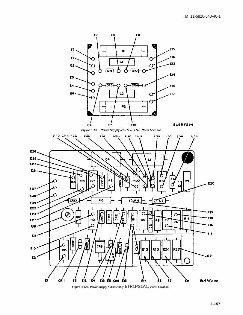
Figure 3-127
TM 11-5820-540-40-1
Figure 3-122. Power Supply Subassembly 5TR1PS1A1, Parts Location.
3-157

TM 11-5820-540-40-1
Figure 3-123. Voltage Regulator Amplifier 5TR1PS1AR1AR1, Parts Location
(7) Release S5 and S7. Meter M1 should indicatebetween 40% and 80% Note the indication on meterMl.
(8) Turn switch S4 to the +28 V METER posi-tion. Press and hold S5 and S7. Meter M1 should indi-cate the same as in (6) above. If necessary, adjust R17(fig. 3-123) for the proper indication. Release S5 andS7. Meter M1 should indicate approximately the sameas noted in (8) above.
(9) Turn switch S4 to the +12 V position. Con-nect the digital multimeter to J6 (+) and J2 (—). Pressand hold S5 and S7. The digital multimeter shouldread 12.0 ±0.2 Vdc. If necessary, adjust R13 (fig. 3-123) for 12.0 Vdc. Record the digital multimeter read-ing. Note the indication on meter M1.
(10) Release S5 and S7. The digital multimetershould indicate 12.0 Vdc to 12.5 Vdc. Note the indica-tion on meter M1.
(11) Turn switch S4 to the +12 V METER posi-tion. Press and hold S5 and S7. Meter M1 should indi-cate the same as in b(10) above. If necessary, adjustR20 (fig. 3-123) for proper indication.
(12) Release S5 and S7. Meter M1 should indicateapproximately the same as in (10) above.
(13) Adjust the voltage control on the PP-6304 to105 Vac and press and hold S5 and S7. The digital mul-timeter reading should be within ±0.2 Vdc of the readingrecorded in b(9) above.
(14) Release S5 and S7. Adjust PP-6304 to 115 Vacand set test facility switches S1 and S2 to OFF.
(15) Reinstall special purpose cables W2 and W3into the transmitter test facility and close POWER SUP-PLY door.
(16) Seal R10, R17, R13, and R20 as described inparagraph 2-12.
(17) Replace both covers on unit under test.
3-158

TM 11-5820-540-40-1
c. Troubleshooting (FO-25). If +12 and 28 voltmeter 3-29. Power Supply (Chassis) 5TR1PS1indications are abnormal, isolate the defective compo- a. Test Equipment and Material Required.nent or components by making in-circuit voltage and Equipment Common nameresistance measurements, using allocated digital mul- Test Facility, Transmitter Transmitter test facilitytimeter. Typical in-circuit resistance measurements are TS-2866(V)2/GRM-95(V)2shown in chart below. Accessory Kit, Test Facilities Set Accessory kit
MK-1173(V)2/GRM-95(V)2Test Facility, RF Modules, Test facility, rf modules
TS 3837(V)2/GRM-95(V)2Impedance Bridge ZM-71/U Impedance analyzerInsulation Tester, CR 1864 Insulation testerDigital Multimter AN/USM-451 Digital multimeterOscilloscope AN/USM-281C OscilloscopeVoltmeter, Electronic ME-459/U VTVM
I I Base (–) I Base (+)
I Translator I Emitter (+) Collector (i-) I Emitter (–) Collector (–)
Res Res(ohms) Range (ohms) Range
Res Res(ohms) Range (ohms) RangeType
12 V regulator Q128 V regulator Q212 V regulator Q328 V regulator Q412 V regulator Q5
2N6972N6972N6972N6972N697
15k 20k 20M3500 20k 75k 20M1800 2k 15k 20M8500 20k 1200 2k300k 20M 300k 20M
800 2k 740 2k780 2k 740 2k760 2k 700 2k780 2k 700 2k780 2k 700 2k
b. Test Procedure. (4) Set the test facility switches as follows:Switch Position
S1 ONS20 S4
S4 +12 V METER
(5) Set test facility switch S4 to all position; moni-tor the indications on meter M1 as follows:
(6) Connect the digital multimeter between FL24(+) and a convenient ground (–).
(1) Open the test facility power supply hinged coverand remove the jumper cables.
(2) Connect the test equipment as shown in figure3-124. Set power supply PP-6304/GRM-95(V) to 115Vac as indicated on the panel voltmeter.
(3) Place the unit under test in front of the air outletso that the airflow will be directed over the heat sink.
S4 position Auxiliary operation Ripple
VTVMM1 reading
(%)
J6J12J9
*FL20
*FL22
+12 V METER+28 V METER+26 V
OUTPUT FIL
DRIVER FIL
Press S5 and S7Press S5 and S7Press S5, S7 and
S3Press S5, S7 and
S3Press S5, S7 and
S3
J2J2J2
*FL21
*FL23
12 ±0.228.0 ±0.226 ±1.3
8.2 ±0.8
8.2 ±0.8
40-6045-5545-55
50-70
50-70
45-55
Greenband
Greenband
Greenband
<3.5 mV<3.5 mV<350 mV
<120mV
<120mVaboveOUT-PUTFIL
<17 mV600 V Set S2 to OFF,press and holdS3, set S2 toON.
DRIVER CUR
OUTPUT CUR
26 VAC
* NOTE: See Figure 3-115 for test point location on unit under test.
3-159

TM 11-5820-540-40-1
Figure 3-124. Power Supply (ChassLs) 5TR1PS1, Test Setup.
3-160

TM 11-5820-540-40-1
(7) Set test facility switch S4 to 600 V METER (9) Ifnecessary adjust R18 on the unit under testposition and set S2 to OFF. for a 50 percent indication on M1 meter.
(8) Press and hold switch S3, set switch S2 to ON (10) Release switch S3 and set switch S2 to OFF.and adjust the voltage control on the power supply PP- (11) Return the voltage control on power supply6304 until the digital multimeter indicates +630 V ±1 PP-6304 to 115 Vat.V. Meter Ml should indicate 50 percent of full scaledeflection. c. Troubleshooting (FO-25).
WARNING
HIGH VOLTAGE is accessible at the connectors and test leads of the insulation tester. Ensure thatthe test switch is in the “DISCHARGE” position before handling test connections.
Symptom Probable cause Checks and corrective measures
1. Test facility switch S1 trips and will Short circuit on the input side, E51 failure a. Check lightning arrestor E51 (fig. 3-115)not reset. or conductor shorting to ground. for short circuit.
b. Check C1 for short circuit Observepolarity when connecting the digitalmultimeter. Digital Multimeter shouldindicate 20k ohm minimum.
c. Using the insulation tester, check T2, T1,and associated components. Disconnectthe heat sink connect the positive leadof the insulation tester to L1 pins 1 and4 in turn and the negative lead to thechassis, set the insulation tester controlsto 500 V and MEASURE. Reset toDISCHARGE before moving test leads.The insulation tester meter shouldindicate 100 megohms minimum. IsolateT1 by disconnecting leads at T1 pins 5and 16. Replace components asrequired.
2. Test facility switch S1 remains on. No Starting circuit not operating.M1 meter indication for any positionof S4.
3. No meter indication in the 600 V a. Relay K2 not operatingposition.
b. Open circuit
4. No meter indication in 600 V position, a. CR15 defective+12 V and +28 V tripped on 600 Vtest. b. T3 shorting to ground.
5. Test facility meter reads 30% or less in R48 not bypassed600 V position.
Check starting pulses across E17 and E18,then E18 and E9, (figure 3-122) on5TR1PS1A1. Use an oscilloscope to ob-serve a 70 volt pulse, 10 tQ 30 milli-seconds long, immediately after testfacilitiy switch S2 is turned on If thesepulses are not present check the opera-tion of relay K1 and associated circuits.
NOTE
On oscilloscope use the ADD mode displaywith the right channel inverted and 2 volts/divvertical scale for 10:1 probes.
a. Check operation of relay K2; replace ifnecessary.
b. Check components in the 600 V circuit foropen circuit.
a. Check CR15 for short circuit, replace ifnecessary.
b. Check T3 and replace if necessary.
Check operation of relay K4 and replace ifnecessary.
3-161
TM 11-5820-540-40-1
c. Troubleshooting. – ContinuedSymptom Probable cause checks and correctiue measures
6.
7.
8.
9.
10.
11.
12.
13.
14.
26 Vac normal; abnormal indications inall other positions of S4.
Low indication with switch S4 inDRIVER FIL (or OUTPUT FIL)positions.
Abnormal reading with switch S4 inDRIVER CUR position. Normal read-ings at FIL positions.
Abnormal reading with switch S4 inOUTPUT CUR position. Normalreading at OUTPUT FIL position.
+12 V and +28 V ripple measurementhigh.
+26 V ripple measurement high
Driver heater and/or output heaterripple measurement high.
600 V ripple measurement high.
Abnormal indication, S4 in 600 VMETER position. 600 V positionnormal.
a. Defective component in secondary ofT2.
b. 5 kHz inverter circuit defective.
Defective FL29, 5TR1PS1PS1, or T2.
Defective CR15.R21 or 23
Defective CR14, R19 or R20.
Leaky or open filter capacitor C19.
Leaky or open filter capacitor C20 or C4.
Defective 5TR1PS1PS1 and FL29.
Defective C6
600 V METER circuit defective.
a. Check T2 secondary circuits for shorts.
b. Check T2 primary circuit components.
Check 5TR1PS1PS1, FL29 and T2.
Check CR15,R21 and/or R23. Replace asrequired.
Check CR14, R19 and/or R20. Replace asrequired.
Check and replace C19 if necessary.
Check capacitor. Replace as required
Check 5TR1PS1PS1 and FL29.
Check and replace C6 if necessary.
Check CR13 and R14 through R18(5TR1PS1A1).
3-30. Transmitter Case 5A2 (CY-4637/GRC-103
a.
(V) or CY-4637A/GRC-103(V))
NOTE
The following procedure checks the con-tinuity and insulation resistance of theinterconnecting cable between the freedhead and the RF head of the transmitter.
Test Equipment and Material Required.
Equipment
Test Facility, Transmitter,TS-2866(V)2/GRM-95(V)2
Accessory Kit, Test Facility SetMK-1173(V)2/GRM-95(V)2
Multimeter, Digital AN/USM-451Test Set, Insulation GR-1864Power Decade Resistor ZM-58/UTest Facility, Radio Frequency
Modules TS-3837(V)2/GRM-95(V)2
Common name
Transmitter test facility
Accessory kit
DMMMegohmmeterDecade resistorRf module test
facility
b. Test Procedures.
1.
NOTE
Before performing the following tests.
Disconnect fan assembly 5A2B1 andtest as described in paragraph 3-33.2. On CY-4637A model units, remove tem-perature control monitor 5A2A2 and test asdescribed in paragraph 3-32.3. On CY-4637 plain model units discon-nect and insulate the lead from E3 of dif-ferential pressure monitor 5A2A2AR1(units incorporating ECP 13 have a ground-ing lug attached to E3).Do not reconnect the assemblies aboveuntil instructed to do so.
(1) Interconnecting wiring tests.(a) Connect the equipment
figure 3-125.as shown in A,
3-162

Figure 3-125.
TM 11-5820-540-40-1
3-163

TM 11-5820-540-40-1
(2) Continuity tests - Continued
5A2A1J4(FDM)Pin A to 5A2A1J6
and 5A2A1J7and 5A2A1P1
Pin B to 5A2A1J6and 5A2A1J7and 5A2A1P1
Pin C to 5A2A1J6and 5A2A1J7
Pin D to 5A2A1J7
5A2A1J5 (CY-4637/GRC-103(V) only)Pin 1 to 5A2A1J7Pin 2 to 5A2A1J7Pin 3 to 5A2A1J7
5A2A1J6Pin 21 to 5A2A1J7Pin A2 to 5A2A1J7outer shell
5A2A1P1(CY-4637A/GRC-103(V) only)Pin 1 to 5A2A1J7Pin 2 to 5A2A1J7Pin 3 to 5A2A1J8Pin 4 to 5A2A1J8Pin 5 to 5A2A1J6Pin 6 to 5A2A1J6Pin 8 to 5A2A1J6Pin 9 to 5A2A1J5Pin 10 to 5A2A1J5Pin 11 to 5A2A1J7
(3) Insulation test.
Pin 41Pin 4Pin 15(CY-4637Aonly)
Pin 46Pin 5Pin 7(CY-4637Aonly)
Pin 11Pin 1
Pin 3
Pin 14Pin 15Pin 11
Pin 2Pin A2outer shell
Pin 15Pin 14Pin 27Pin 26Pin 17Pin 43Pin 19Pin 1Pin 2Pin 11
HIGH VOLTAGE is accessible at the con-nectors and test leads of the Megohmmeter.Ensure that the test switch is in the“DISCHARGE” position before handlingtest connections.
(a) Connect the test equipment as shown in B,figure 3-125.
(b) Set the Megohmmeter controls to“measure” and “200 volts”.
(c) Set S2 (test set) to positions 1 thru 43. Foreach position of S2 rotate S1 through a completerevolution.
(d) The megohmmeter shall indicate more than100 megohms EXCEPT when S1 and S2 positions
match (and, for CY-4637/GRC-103(V), EXCEPT thepositions described in paragraph (1)(c) 2. and 3.above).
(e) Connect the test equipment as shown in C,figure 3-125 and set S2 to position 46 (CY-4637/GRC-103(V), only).
(f) Connect the test probe to each pin of P1(except pin 11). For each connection rotate S1 to posi-tion 1 thru 45. The megohmmeter shall measure 100megohms or more except in one of the followingpositions; 17, 19, 39, 41 or 43, corresponding to P 1pins 5, 8, 15, 6, or 7, respectively (CY-4637A/GRC-103(V) only).
(g) Set megohmmeter to DISCHARGE.(h) Connect the megohmmeter “-” terminal to
5A2A1J6 pin 1 and the “+” terminal to 5A2A1J7 pin11 (chassis ground) with test lead CMC 267-800015-000 (4 W15).
(i) Set the megohmmeter to 1000 V and then toMEASURE. The megohmmeter should indicate morethan 100 megohms. Set the megohmmeter toDISCHARGE.
(j) Set the megohmmeter to 200 V. With themegohmmeter “+” terminal connected to 5A2A1J7pin 11, connect the “-” terminal to 5A2A1J7 pins 6through 10, in turn. For each connection set themegohmmeter to MEASURE, not the megohmmeterindication and reset the megohmmeter to DIS-CHARGE. The megohmmeter should indicate 100megohms or more to each connection checked.
(k) Connect the megohmmeter between thecenter contact and the shield of 5A2A1J6 pin 2 withthe red lead of test lead CMC 267-800015-000(4W15), test lead CX-12044/U (1W36) and adaptor-connector UG-1878/U (1CP10).
(1) Set the megohmmeter to MEASURE. Themegohmmeter should indicate 100 megohms or more.Set the megohmmeter to DISCHARGE.
(m) Disconnect transmitter case from the testequipment.
(4) Checking depth of connectors.(a) Use fixed Depth Gage TL-766/GRM-95(V)
(3MP2) to check the proper depth of connectors J7and J8. With the top of the gage resting on the frontedge of the case, the bottom of the gage should barelytouch the connectors. Install locally manufacturedshims under each end of the retaining plate when thiscannot be attained.
(b) Use fixed Depth Gage TL-768 (3MP4) tocheck the proper depth of connector J6. With the topof the gage resting on the front edge of the case, thebottom of the gage should barely touch the shouldersof the bushing around J6. Install washers between J6and the case when this cannot be attained.
WARNING
3-164

TM 11-5820-540-40-1
(5) Overheat lamp and blower operational test. (2) Abnormal indications in b. (3) above may be(a) Reconnect blower 5A2B1 and differential caused by pinched wires or by contaminants in the
pressure’ monitor 5A2A2AR1 (CY-4637) or tempera- cables or connectors.ture control monitor 5A2A2 (CY-4637A). (a) Identify faulty connection(s).
(b) CY-4637IGRC-103(V), only. (b) Remove, clean, and dry distribution box1. Install a working T-983 and AM-4320 in 5A2A1, cables, and connectors.
the unit under test and connect the Dummy Load to (c) Retest after completely dry.the AM-4320 PWR OUT connector, and the Power (d) Replace or repair any remaining faultyCable to 5A2A1J1 and a 115 Vac Power Source. parts.
2. Turn the T-983 Power ON/RESET to (3) Abnormal indications in b. (5)(b) above areON. The OVERHEAT lamp should light and go out probably caused by a faulty differential pressure mon-within ten seconds. itor 5A2A2AR1.
3. Block the T-983 transmitter air intakecompletely. The OVERHEAT ALARM lamp shouldlight.
4. Block the air intake approximately 50%.The OVERHEAT alarm lamp should not light.
5. Remove T-983, AM-4320 and testequipment.
(c) CY-4637A/GRC-103(V.), only.1. Install a working T-983 in the unit under
test. Connect the Power Cable to 5A2A1J1 and to a115 Vac Power Source.
2. Connect the decade resistor between
3-31. Distribution Box 5A2A1
a. Refer to paragraph 2-38 for replacementinstructions.
b. Test as described in paragraph 3-30 (as appro-priate) except:
(1) Connect the shell of connector J6 and theground lead of test set TS-2870/GRM-95(V) to thechassis of distribution box 5A2A1.
(2) Change or add point to point continuitychecks as listed below
5A2A1J6, Pin 17 and 43. Connect a jumper between5A2A1J6, pins 18 and 19. Adjust the decade resistor
From To
to 2 megohms. wire (removed from 5A2A1J 1 pin A) 5A2A1J7 pin 63. Turn the T-983 Power ON/RESET to shield wire (removed from 5A2A1J1 5A2A1J7 pin 11
ON. Set the meter selector switch to 600 V position. pin B)The blower motor should operate at full speed and wire (removed from 5A2A1J1 pin C) 5A2A1J7 pin 7
meter Ml should read 80% or greater. TheOVERHEAT light should be on.
CY-4637/GRC-103 ONLY
4. Adjust the decade resistor to 300 K and 5A2A1J8 pin 27 to 5A2A1AR1E47.5 K ohms in turn. The blower motor should not 5A2A1J8 pill 3 to 5A2A1AR1E3operate and the OVERHEAT light should be off. or
5. Adjust the decade resistor to 4.8 K ohms. ground terminal to 5A2A1AR1E3
The blower motor should operate at medium speed.6. Adjust the decade resistor to 800 ohms. 3-32. Control Monitor Temperature Sensor,
The blower motor should operate at maximum speed. 5A2A27. Adjust the decade resistor to 600 ohms.
The OVERHEAT light should be on. a. Test equipment and material required.
8. Adjust the decade resistor to 400 ohms. Name DescriptionMeter Ml indication should drop to zero.
9. Remove T-983 and test equipment. Transmitter Test Facility Transmitter test facilityTS-2866(V)2/GRM-95(V)2
Oscilloscope AN/USM-281C Oscilloscopec. Repairs (FO-5, FO-6 or FO-26).
(1) If an abnormal indication is obtained in the b. Test Procedures (Fig. 3-126 thru 3-128).tests in paragraph b. (1) or (2) above, use the TS-2870/GRM-95(V) schematic (TM 11-6625-1696-14) in con- (1) Connect the test equipment as shown in figurejunction with the appropriate unit schematic to 3-127.identify the faulty connection(s), remove distribution (2) Set oscilloscope display to ADD and the rightbox 5A2A1, and repair or replace the faulty connec- hand channel to INVERT. Set vertical sensitivity to 10tor(s) or wire(s). - v/cm on each channel.
3-165

TM 11-5820-540-40-1
Figure 3-126. Transmitter Case, Continuity Check, Test Setup.
3-166

TM 11-5820-540-40-1
Figure 3-127. Control Monitor Temperature Sensor, 5A2A2, Speed Control, Test Setup.
Figure 3-128. Control Monitor Temperature Sensor, 5A2A2, Waveform.
3-167

TM 11-5820-540-40-1
(3) Set the power supply to 115 Vac as indicatedon its panel voltmeter.
(4) On the transmitter test facility, set S1 to ONand S33 to OFF. Test facility blower should operate.
Test facilityS33 position Blower speed
OFFFAIL 1FAIL 2ZERO SPEED 1ZERO SPEED 2MAX SPEED 1MAX SPEED 2ALARMTRIP
MAXMAXMAXOFFOFFMAXMAXMAXMAX
(5) Observe the test facility blower operation,oscilloscope display, alarm lamp and trip lamp con-ditions, for correct conditions while varying S33 posi-tion as indicated in table below.
Alarm Trip Oscilloscope displayLamp Lamp (fig. 3-148)
OFF OFF NO DISPLAYON OFFON ON
OFF OFF NO DISPLAYOFF OFF NO DISPLAYOFF OFFOFF OFFON OFFON ON
c. Troubleshooting (FO-27).Symptom Probable cause Checks and corrective measures
Blower fails to operate at any position of a. Failure of 26 V supply. a. (1)switch S33.
(2)
(3)
Blower fails on FAIL 1.
b. Failure of 6.2 V supply.
c. Failure of 15 V supply.
Speed control circuit defective.
b. (1)
(2)
(3)
c. (1)
(2)
(3)
(4)
Check for approx. 20 V at E 12 of board A2except at OFF and ZERO SPEED 1and 2 positions of S33. If voltage is +26V, check Q3 mounted on heat sink (fig.3-129) and replace if defective.
Check for +26 Vat E12 at OFFand ZERO SPEED 1 and 2 positionsof switch S33.
Check for +26 Vat pin 14 of J1 and R15of board Al (figure 3-130).
Check test point E7 of board Al for 6.2 Vat all positions of S33 except OFF(fig. 3-130).
Check test point E11 of board A2 for 6.2Vat all positions of S33 except OFF(fig. 3-134).
Check CR1 and R1 of board A2 for 6.2 Vat all positions of S33 except OFF(fig. 3-131).
Check 15 V at E1 of board A2 (fig. 3-131).
Check 15 V at E5 of board A1 (fig. 3-130).
Check A3 of board A2 and associated com-ponents (fig. 3-131).
Check Q3 (2N 3749) on board A2 (fig.3-131).
a. Check for approx. +3 Vat E5 of board A2(fig. 3-131). If voltage is high, check A3and CR6 of board A2. If voltage is low,check for square wave of approx. 15 Vp-pamplitude at collector of Q1 and at pins1,5,8, 11 and 14 of A2 on board A2.
3-168

TM 11-5820-540-40-1
Figure 3-129. Control Monitor Temperature Sensor, 5A2A2, Parts Location
c. Troubleshooting (FO-5). – Continued
Symptom Probable cause Checks and corrective measures
b. Check for approx. 15 Vp-p square waveat pins 8 and 15 of A1 on board A2(fig. 3-131).
c. Check for approx. 15 Vp-p square waveat collector of Q2 and Q3 on board A2(fig. 3-131).
d. Check for approx. 15 Vp-p square waveat E2 and E4 of board A3. If presentcheck Q1, Q2, T2 and T3 on boardA3 (figs. 3-129 and 3-132).
Blower fails on FAIL 2. Speed control circuit defective. Check A1 on board A1 (fig. 3-130).
Blower operates but alarm not activated Defective components in relay circuit- s. Check A2 and Q2 on board A2 (fig. 3-131).or blower operates but trip lamp not b. Check A2, Q1 and K1 on board A1 (fig.activated. 3-130).
NOTE
Replace all defective components found during troubleshooting.
3-33. Centrifugal Fan 5A2B1a. Test Equipment and Material Required.
(2) Set the power supply to 115 Vac as indicatedon its panel meter.
(3) Set switch S1 to ON and hold switch S19 inEquipment Common name the TEST position. The fan should rotate at full speed.
Release S19, and set S1 to OFF.Test Facility, Transmitter Transmitter test facility (4) Using the digital multimeter, measure the re-
TS-2866(V)2/GRM-95(V)2.Accessory Kit, Test Facilities Set Accessory kit
MK-1173(V)2/GRM-95(V)2.Multimeter, Digital AN/USM-451 Digital multimeter
b. Test Procedure.(1) Connect test equipment as shown in figure
133.
sistance between pins of 5A2B1P1 as indicated intable below.
Multimeter leads at pins: Resistance
1 and 2 40 –10, +20 ohms3- 1and3
2 and 3
3-169

TM 11-5820-540-40-1
Figure 3-130. Control Monitor Temperature Sensor, 5A2A2A1, Parts Location.
Figure 3-131. Control Monitor Temperature Sensor, 5A2A2A2, Parts Location.
3-170

TM 11-5820-540-40-1
Figure 3-132. Control Monitor Temperature Sensor, 5A2A2A3, Parts
Figure 3-133. Centrifugal Fan 5A2B1, Test Setup.
Location.
3-171

TM 11-5820-540-40-1
Section Ill. RECEIVER–TRANSMITTER ORDER WIRE
RT-773/GRC-103(V)
3-34. Recevier Transmitter Order Wire RT-773/GRC-103(V) Alinement
a. Test Equipment and Material Required.
Equipment Common name
Test Facility, Transmitter Transmitter test facilityTS-2867(V)2/GRM-95(V)2
Accessory Kit, Test Facilities Set Accessory kitMK-1173(V)2/GRM-95(V)2
Generator, Signal AN/USM-205A Wide range oscillatorVoltmeter, Electronic ME-459/U VTVMCounter, Electronic TD-1225-(V)1/U Counter
b. Test Procedures.NOTE
Ensure that the PCM/FDM switch is in thePCM position on board A4 and the buzzeris in ALM NORM. This is accomplished byremoving the front panel of the unit undertest. Leave the panel off the case for thefollowing tests.
(1) Connect the test equipment as shown in A offigure 3-134.
NOTE
Set and maintain the power supply at 115Vac as indicated on its panel voltmeter.
(2) Set test facility switches S1 to ON and S31 toSET REF.
(3) On the unit under test the POWER lampshould light
(4) Disconnect the cable from test facility J45(TO RADIO) connector. The POWER lamp shouldremain lit. Reconnect the cable to the test facility.
(5) Disconnect the cable from test facility J44(PATCH THRU) connector. The POWER lampshould remain lit. Reconnect the cable to the testfacility.
(6) Set the wide range oscillator to 1 kHz asindicated on the counter and adjust the level to —10dBm as indicated on the VTVM.
(7) Set switch S31 to position A TO B and thenposition B TO A. In both positions the VTVM shouldindicate –10 dBm ±0.2 dB. A 1 kHz tone should beheard in the handset of the unit under test.
(8) Set switch S31 to SET REF position. Set thewide range oscillator to 1600 Hz ±4 Hz, as indicatedon the counter and adjust the level to – 13 dBm asindicated on the VTVM.
(9) Set switch S31 to A to B then B to A. On theunit under test the CALL lamp should light and thebuzzer should sound in both positions.
(10) Set BUZ/ALM NORM switch S2 on the unitunder test to BUZ OFF. The buzzer should be silen-ced. The CALL lamp should remain lit, but with theillumination dimmed.
(11) Set the BUZ OFF/ALM NORM switch S2 toALM NORM.
(12) Disconnect the cable from connector J43 onthe test facility.
(13) On the handset of the unit under test pressthe PRESS-TO-TALK switch and speak into the mic-rophone. You should be able to hear your own voice inthe receiver of the handset. The VTVM should give anindication while you are speaking, for both the A TO Band B TO A position of switch S31.
(14) Connnect the counter as shown in B, figure 3-134. On the unit under test, press and hold the RINGbutton, and set test facility switch S31 from position ATO B to B TO A. The VTVM should indicate – 10dBm ±1.0 dB, in both the A TO B and B TO A posi-tion of switch S31. The counter should indicate 1600Hz ±1 Hz.
(15) Reinstall panel 9A2 to case CY-4635.c. Troubleshooting Procedure. Refer to the
troubleshooting chart in paragraphs 3-35 through 3-38.
3-35. Distribution Panel 9A1
a. Test Equipment and Material Required.
Equipment Common name
Test Facility, Transmitter Transmitter test facilityTS-2866(V)2/GRM-95(V)2
Accessory Kit, Test Facilities Set Accessory kitMK-1173(V)2/GRM-95(V)2
Multimeter, Digital AN/USM-451 Multimeter
b. Test Procedure.(1) Using the multimeter, check resistances be-
tween the points listed below. Refer to figures 3-135and 3-136.
3-172

TM 11-5820-540-40-1
Figure 3-134. Order Wire Operational Check, Test Setup.
3-173

TM 11-5820-540-40-1
Figure 3-135. Receiver- Transmitter Order Wire Unit Distribution Panel 9A1.
NOTE
9A1J2 is PATCH THRU and 9A1J1 isTO RADIO.
Multimeter Resistanceconnected between (ohms)
9A1J1 pin G and 9A1J1 pin K (R2) 620 ±6O9A1J2 pin K and 9A1J2 pin G (R1) 620 ±609A1J2 pin A and 9A1P1 pin 6 <19A1J2 pin B and 9A1P1 pin 13 <19A1J2 pin C and 9A1J3 pin A <1
(2) Connect the test equipment as show-n in figure3-137.
NOTE
Set and maintain the power supply outputat 115 Vac as indicated on its panelvoltmeter.
(3) Set test facility switches S1 to ON and S31 toA TO B.
(4) Using the multimeter, check voltages betweenthe points listed below. Refer to figure FO-13.
Multimeter connections Indication(+) (-) (Vdc)
9A1P1 pin 6 9A1P1 pin +26 ±1.313
9A1J3 pin A 9A1J3 pin B +12 ±0.2
3-174

TM 11-5820-540-40-1
Figure 3-136. Receiver- Transmitter Order Wire, Unit 9.
(5) Short circuit 9A1P1 pins 3 and 13. The buzzer (9) Release the handset switch the multimetershould sound. indication should return to infinity.
(6) Set test facility switches S31 and S1 to OFF. (10) Repeat (8) and (9) above three times.(7) Connect the multimeter across 9A1TB1 pins (11) Connect the multimeter to 9A1TB1 pins 2
4 and 5. It should indicate infinity. and 3 and repeat (7) through (10) above.(8) Press the handset PRESS-TO-TALK switch
the multimeter should indicate <3 ohms. c. Troubleshooting (FO-13).
Symptom Probable cause Checks and corrective measuresAbnormal indication of R1 and R2 (b. (1) Defective resistor assembly 9A1A1. Check resistors on resistor assembly 9A1A1above). (FO-13). (R1 is connected between El and
E2. R2 is connected between E3 and E4.)Replace resistor assembly 9A1A1 asrequired.
Abnormal indication between 9A1J2 Defective wiring or relay K1. Check wiring between 9A1J2 and 9A1P1(PATCH THRU connector) pins and and reIay K1 contacts If wiring is9A1P1 pins (b. (1) above). normal, replace relay K1.
3-175

TM 11-5820-540-40-1
Figure 3-137. Distribution Panel 9A1, Test Setup.
c. Troubleshooting. -Continued
Symptom Probable cause Checks and corrective measures
Abnormal indication between 9A1J2 Defective wiring or relay K2. Check wiring between 9A1J2 pin C and(PATCH THRU connector) pin C 9A1J3 pin A and relay K2 contacts Ifand 9A1J3 pin A (b. (1) above). wiring is normal, replace relay K2.
Abnormal indication when checking volt- Defective wiring or relay K1. Check wiring between 9A1P1 pin 6 and pin 3age between 9A1P1 pin 6 and 9A1P1 pin and relay K1 contacts. If wiring is nor-13 (b. (4) above). real, replace relay K1.
Abnormal indication when checking volt- Defective wiring or relay K2. Check wiring between 9A1P3 pin A and pin Bage between 9A1P3 pin A and 9A1P3 pin and relay K2 contacts. If wiring is nor-B (b. (4) above). mal, replace relay K2.
Buzzer 9A1DS1 does not sound (b. (5) Defective buzzer 9A1DS1. Replace buzzer 9A1DS1.above).
Abnormal indication when testing hand- Defective handset switch. Replace handset switchset switch (b. (6) through (10) above).
3-176

TM 11-5820-540-40-1
3-36. Monitor Panel 9A2a. Test Equipment and Material Required.
Equipment Common name
Multimeter, Digital MultimeterAN/USM-451
b. Test Procedure.(1) Using the multimeter, check resistances to
validate operation of switch 9A2S1 (fig. 3-136) asfollows:
ResistanceMultimeter connected Secondary (ohms)
between following action infinity
9A2S1 pins7 and 27 and 2 press S1 <17 and 1 <17 and 1 press S1 infinity6 and 3 infinty6 and 3 press S1 <16 and 4 <16 and 4 press S1 infinity
(2) Using the multimeter check the operation ofswitch 9A2S2 as follows:
Connect multimeter Secondary Resistancebetween action (ohms)
9A2J2 pin 59A2J2 pin 3 S2 OFF9A2J2 pin 59A2J2 pin 3 BUZZ ALM <19A2J2 pin 5 9A2A1E4 NORM9A2J2 pin 59A2A1E4 S2 OFF 200 *5
S2 ALM NORM <1
(3) Using the rnultimeter, check resistance ofresistors on resistor assembly 9A2A1 as indicated inthe table below.
Multimeter connected between Resistance
E1 and E4 100 *5%E5 and E3 100 *5%
(4) If normal indications are obtained during testprocedures carry out the troubleshooting proceduresoutlined inc. below.
C. Troubleshooting (FO-13).
3-37. Telephone Signal Converter 9A3a. Test Equipment and Material Required.
Equipment Common name
Test Facility, Transmitter Transmitter test facilityTS-2866(V)2/GRM-95(V)2
Accessory Kit, Test Facilities Set Accessory kitMK-1173(V)2/GRM-95(V)2
Generator, Signal AN/USM-205A Wide range oscillatorMultimeter, Digital AN/USM-451 MultimeterCounter, Electronic Digital Read- Counter
out TD-1225(V)1/UElectronic Voltmeter ME-459/U VTVM
b, Test Procedure.(1) 1,600 Hz tone generation.
(a) Connect the test equipment as shown infigure 3-138.
NOTE
Set the power supply to 115 Vac asindicated on its panel voltmeter. Maintainthis setting throughout the followingprocedures.
(b) Set test facility switch S1 to ON and switchS32 to OSC. The VTVM should indicate 1.6 V ±0.1 V.On the unit under test adjust gain control R13 (fig. 3-139) to obtain 1.6 V ±0.1 V indicated on the VTVM.
(c) The counter should indicate 1,600 Hz ±1Hz. Adjust C4 on the unit under test to obtain the cor-rect frequency.
(d) Set switch S32 to OFF.(2) 1,600 Hz tone receive gain and tuning
measurement.(a) Connect the test equipment as shown in
figure 3-140.(b) Set test facility switch S32 to the RCVR
position.(c) Set the coaxial to position 1.(d) Tune the wide range oscillator to 1,600 HZ
±1 Hz, as indicated on the counter and adjust the out-put level to obtain a 100 mV indication on the VTVM.
Symptom Probable cause Checks and corrective measures
Abnormal indication in b. (1) above. Defective 9A2S1. Replace switch 9A2S1.
Abnormal indication b. (2) above. Defective 9A2S2. Replace switch 9A2S2.
Abnormal indication in b. (3) above. Defective resistors R1, R2 or R3. Replace resistor assembly 9A2A2.
3-177

TM 11-5820-540-40-1
Figure 3-138. Telphone Signal Converter 9A3, 1600 Hz Tone Generation Test Setup.
(e) Set the coaxial stitch to position 2. Vary thewide range oscillator frequency for maximum indica-tion on the VTVM (peak). The frequency indicated onthe counter should be 1,600 Hz ±1 Hz. Note theindication.
(3) 1,600 Hz tone detector sensitivity/selectivitymeasurement.
(a) Connect the test equipment as shown infigure 3-140.
(b) Set the coaxial switch to position 1.(c) Adjust the output level of the wide range
oscillator to 50 mV as indicated on the VTVM. Main-tain wide range oscillator frequency at 1,600 Hz ±1 Hzas noted in (2)(e) above.
(d) Set test facility switch S32 to the ALARMposition.
(e) Slowly increase the output level of the widerange oscillator until the order wire ALARM lamp onthe test facility lights. The VTVM should indicate 108mV ±5 mV.
(f) Adjust the output level of the wide rangeoscillator to 200 mV as indicated on the VTVM.
3-178
(g) Set the frequency of the wide rangeoscillator to 1,550 Hz as indicated on the counter.
(h) Slowly increase the frequency of the widerange oscillator until the order wire ALARM lamp onthe test facility lights. The frequency indicated on thecounter should be 1,580 Hz ±10 Hz.
(i) Repeat step (f) above and adjust frequencyof wide range oscillator to 1,650 Hz.
(j) Slowly decrease the frequency of the widerange oscillator until the order wire ALARM lamp onthe test facility lights. The frequency indicated on thecounter should be 1,620 Hz ±10 Hz.
c. Adjustments.(1) 1,600 Hz tone receive tuning adjustment
(a) Repeat paragraph b. (2)(a) through(e).(b) Adjust C2 on the unit under test for a max-
imum indication on the VTVM.
NOTE
If a sharp peak cannot be obtained byadjusting C2, turn R1 several turns coun-terclockwise and repeat step b. (2)(e).
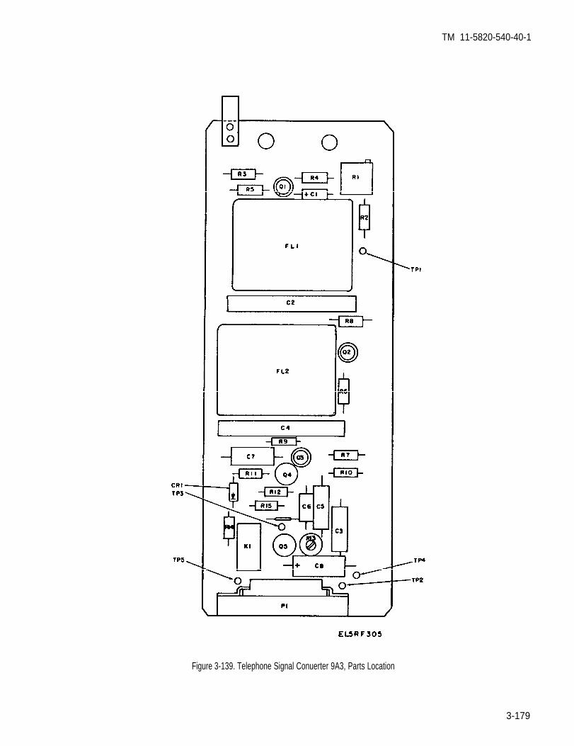
Figure 3-139. Telephone Signal Conuerter 9A3, Parts Location
TM 11-5820-540-40-1
3-179

TM 11-5820-540-40-1
Figure 3-140. Telephone Signal Converter 9A3, 1600 Hz Tone Receive Checks, Test Setup.
(2) 1,600 Hz tone detection and sensitivity/ (b) Repeat paragraph b.(3)(a) through (e).selectivity adjustment (c) Adjust R1 control on 9A3 and repeat b.
(a) Connect test equipment as shown in figure (3)(a) through (e) until required output is obtained.3-140. d. Troubleshooting (FO-13).
Symptom Probable cause Checks and corrective measures
No output (para. b. (1) above). a. Defective CR1. a. Measure the voltage across CR1 (fig. 3-139);the multimeter should indicate 5.6 ±0.2 V.If abnormal indication check CR1 for shortcircuit replace if necessary.
3-180

TM 11-5820 -540-40-1
d. Troubleshooting. -Continued
Symptom Probable cause Checks and corrective measures
Low output: frequency beyond specifiedlimits (b. (2) above).
No output reading (b. (2) above).
Order wire ALARM lamp does not light(b. (3) (e) above).
b. Defective transistor stage Q1, Q2, Q3, b. (1) Using the ac voltmeter, measure the signalQ4, Q5. voltages of transistor stages Q1 through
Q5 (see table in para. e. below).(2) If voltage at Q2 base, or FL2, pin 3 is ab-
normal, check components in Q2 stage,or capacitor C3 for short circuit. Checkcircuit resistance to determine faulty “”component. Replace as required.
(3) If voltage at Q3 emitter is abnormal, checkcomponents in Q3 stage. Replace asrequired
(4) If voltage at TP2 is abnormal check com-ponents in Q4 stage, or resistor R13 foropen circuit. Replace as required.
(5) If voltage at Q1 base and collectorare abnormal replace Q1.
(6) If voltages at Q5 base and collector areabnormal, check Q5 and relay K1.Replace as required
Defective C4 or FL2. Check C4 and FL2; replace if necessary.
a. Defective R1. a. Check continuity of R1, replace if necessary.b. Defective Q1 or FL1. b. Measure the signal voltage of Q1 stage to FL1
pin 3, (see table, para. e. below). Checkcontinuity of FL1. Replace as required.
a Defective transistor Q5. a Measure the voltages at Q5 stage (see table,para e. below).
b. Defective relay K1 or transistor Q5. b. Check the operation of relay K1. If Q5 voltagesare normal K1 contacts may be open withthe relay operated In this case replace K1.
c. Defective C4, FL2, C2 or FL1. c. Check C2 and FL1, or C4 and FL2. Replacedefective components as necessary.
e. Voltage Measurements.
NOTE
Except for the dc measurement, allmeasurements are made with the acvoltmeter, with a 1,600 Hz signal input at alevel of 200 mV, and with the test facilityswitch S32 set to RCVR.
Typical indication (VrmsTestpoint unless otherwise indicated)
Q2-base 0.3FL2-pin3 1.9
Q3-emitter 1.9TP2 1.6
Q1-base 0.080-collector 1.0
FL1-pin3 0.325
Typical indication (VrmsTest point unless otherwise indicated)
Q5-base (TP3)(test facilityset switchS32 set toALARM) 1.6
Q5-collector 2.8 Vdc
3-38. Amplifier Assembly 9A4
a. Test Equipment and Material Required
Equipment Common name
Test Facility, Transmitter Transmitter test facilityTS-2866(V)2/GRM-95 (V)2
Accessory Kit, Test Facilities Set Accessory kitMK-1173(V)2/GRM-95 (V)2
Generator, Signal AN/USM-205A Wide range oscillatorVoltmeter, Electronic ME-459/U VTVMAnalyzer, Distortion AN/URM-184A Distortion analyzer
3-181

TM 11-5820-540-40-1
b. Test Procedure.(1) REC A to TR B thru path.
(a) Connect the test equipment as shown in A,figure 3-141.
NOTE
Set the power supply to 115 Vac asindicated on its panel voltmeter. Maintainthis setting throughout the followingprocedures.
(b) Set switch S1 (fig. 3-142) on the unit undertest to the PCM position and set the coaxial switch toposition 1.
(c) Set the wide range oscillator to 1 kHz at alevel of –10 dBm as indicated on the VTVM.
(d) Set the FUNCTION switch on the distor-tion analyzer to SET LEVEL, the INPUT SEN-SITIVITY control fully clockwise and the meter rangeto –10 dB.
(e) Set test facility switch S1 to ON and S32 tothe OSC position.
(f) Set the coaxial switch to position 2.(g) On the unit under test, adjust control R7
(Level A) to obtain an indication of –10 dBm on theVTVM.
(h) Adjust the distortion analyzer sensitivitycontrols to provide a suitable reference reading. Notethis reading.
(i) Set the distortion analyzer switch toDISTORTION.
(j) Vary the frequency and balance controls toobtain a minimum reading on the distortion analyzermeter. This reading should be at least 40 dB below thereading noted in (h) above. This represents less than1% distortion.
(k) Return the distortion analyzer meter rangeto fully clockwise and the FUNCTION switch to SETLEVEL.
(l) Set switch S1 on the unit under test to theFDM position. The VTVM should indicate less that–50 dB. Return VTVM range switch to –10 dB.
(m) Return switch S1 on the unit under test tothe PCM position
(n) Set the coaxial switch to position 1 and setthe wide range oscillator to 200 Hz at a level of –10dBm as indicated on the VTVM.
(o) Set the coaxial switch to position 2. TheVTVM should indicate within +0.5 dB and –1.0 dB ofthe level adjusted in (g) above.
(p) Repeat steps (n) and (o) above at 250 Hz,500 Hz, 1.5 k.HZ, and 2 kHZ.
(2) REC B to TR A thru path(a) Connect the test equipment as shown in B,
figure 3-141.(b) Repeat steps (b) through (p) of (1) above.
NOTE
In step (g) above, adjust R18 (Level B) con-trol instead of R7.
(3) Handset to TR B transmit path.(a) Connect the test equipment as shown in C,
figure 3-141.(b) Set the coaxial switch to position 1 and set
the wide range oscillator to 1 kHz at a level of 1200 mVon the VTVM.
(c) Set the coaxial switch to position 2. TheVTVM should indicate –10 dBm ±1.0 dB.
(d) Measure the distortion using the methoddescribed in paragraph (1) above, steps (d), (h), (i) and(j). The measured distortion should beat least 34 dBbelow the measured reference (equivalent to less than2% distortion).
(e) Return the distortion analyzer meter rangeto fully clockwise and the FUNCTION switch to SETLEVEL.
(4) Handset to TR A transmit path(a) Connect the test equipment as shown in D,
figure 3-141.(b) Repeat (b) through (e) of (3) above.
(5) REC A to TR A crosstalk.(a) Connect the test equipment as shown in A,
figure 3-143.(b) Set the coaxial switch to position 1 and set
the wide range oscillator to 50 Hz at a level of –10dBm.
(c) Set the coaxial switch to position 2. TheVTVM indication should not exceed –45 dBm.
(6) REC B to TR B crosstalk.(a) Connect the test equipment as shown in B,
figure 3-143.(b) Repeat (b) through (c) of (5) above.
(7) REC A to handset receive path.(a) Connect the test equipment as shown in C,
figure 3-143.(b) Set the coaxial switch to position 1 and set
the wide range oscillator to 1 kHz at a level of –10dBm.
(c) Set the coaxial switch to position 2. TheVTVM should indicate –29.4 dBm ±1.0 dB. Recordthis level.
3-182

TM 11-5820-540-40-1
Figure 3-141.Order Wire Through Circuit Test Setup.
3-183

TM 11-5820-540-40-1
Figure 3-142. Amplifier Assembly 9A4, Parts Location.
3-184

TM 11-5820-540-40-1
Figure 3-143. Order Wire Crosstalk Measurement, Test Setup.
3-185

TM 11-5820-540-40-1
Figure 3-144. 0rder Wire Sidetone, Test Setup.
3-186

TM 11-5820-540-40-1
(d) Disconnect the cable from the 150/600 ohmadapter and reconnect this cable end to J57 on the testfacility. Keep the other end of the cable connected tothe coaxial switch.
(e) Set the coaxial switch to position 1 and setthe wide range oscillator to 1.6 kHz at a level of –10dBm.
(f) Set the coaxial switch to position 2. TheVTVM should indicate 100 mV ±20 mV.
C1
(8) REC B to handset receive path.(a) Connect the test equipment as shown in D,
figure 3-143.(b) Repeat (b) through (f) of (7) above.
(9) Sidetone tests.(a) Set up the test equipment as shown in
figure 3-144.(b) Set the coaxial switch to position 1 and set
the wide range oscillator to 1 kHz at an output level of330 mV as indicated on the VTVM.
(c) Set the coaxial switch to position 2.(d) Remove the 110 ohm load from the VTVM.
The VTVM should indicate 25 mV ±7 mV.
Normal indication Defective componentCheckpoint (m Vrms unless probable cause of
otherwise indicated) abnormal indication
REC A to TB B thru path (Set S32 to OSC)
Q1 base 243Q1 emitter 231 Q1, R2, R3, R4, R5, R6Q2 emitter 9 C2, S1AQ2 base 2.6 VdC R30, R31Q2 collector 288 Q2, R7, R8, R9TP3 235 L1, C3, C4, C5
REC B to TR A thru path (set S32 to OSC)
Q5 base 243 C13Q5 emitter 231 Q5, R26, R27, R28,
R29, R4Q6 emitter 6 C14, SIBQ6 base 2.69 Vdc R30, R31Q6 collector 304 Q6, R11, R19, R32TP9 248 L2, C10, C11, C12
REC A or REC B to handset receive path (set S32 to OSC)
TP6 201 Q1 or Q5 stageTP7 48 T1
Handset to TR A transmit path (set S32 to OSC)
Q4 base 365 C8, R15c. Troubleshooting (FO-13). Q6 collector 480 Q4, R21, R20
507 L2, C10, C11, C12
NOTE Handset to TR B transmit path (set S32 to OSC)
Measurements are taken between the checkQ3 base 366 C8, R15Q2 collector 321 Q3, R1O, R16
point and ground. TP3 260 L1, C3, C4, C5
3-1 87/(3-188 Blank)


By Order of the Secretary of the Army:
CARL E. VUONOGeneral, United States Army
Official: Chief of Staff
WILLIAM J. MEEHAN 11Brigadier General, United States Army
The Adjutant Genera!
DISTRIBUTION:To be distributed in accordance with DA Form 12-51 DS/GS
requirements for AN/GRC-103,A,B(V)1-4.
*U.S..GOVERNMENT PRINTING OFFICE: 1993 - 342 421/61917


PIN: 050483-000