Embed Size (px)
Citation preview
FACULTY DETAILS: Name of the Faculty:: A.Ramesh Babu
Designation: Associate Professor Department:: Computer Science & Engineering
COURSE DETAILS Name Of The Programme:: B.Tech Batch:: 2012
Designation:: B.Tech Year II B.Tech Semester I
Department:: Computer Science and Engineering Title of The Subject Digital Logic Design Subject Code 6753024
No of Students 65
COURSE PLAN
20123-14
Regulation: R11
COURSE PLAN
2012-13
Regulation: R11
FACULTY DETAILS:
Name of the Faculty:: A.Ramesh Babu Designation: Associate Professor
Department:: Computer Science and Engineering
1. TARGET
a) Percentage Pass 100%
b) Percentage I class 85%
2. COURSE PLAN
(Please write how you intend to cover the contents: i.e., coverage of Units by lectures, guest lectures, design exercises, solving numerical problems, demonstration of models, model preparation, or by assignments, etc.)
a) Coverage of units by lectures b) Design exercises c) Assignments
3. METHOD OF EVALUATION
3.1. Continuous Assessment Examinations (CAE 1, CAE 2)
3.2. Assignments / Seminars
3.3. Mini Projects
3.4. Quiz
3.5. Term End Examination
3.6. Others
4. List out any new topic(s) or any innovation you would like to introduce in teaching the subject in this Semester.
Signature of HOD Signature of Faculty Date: Date:
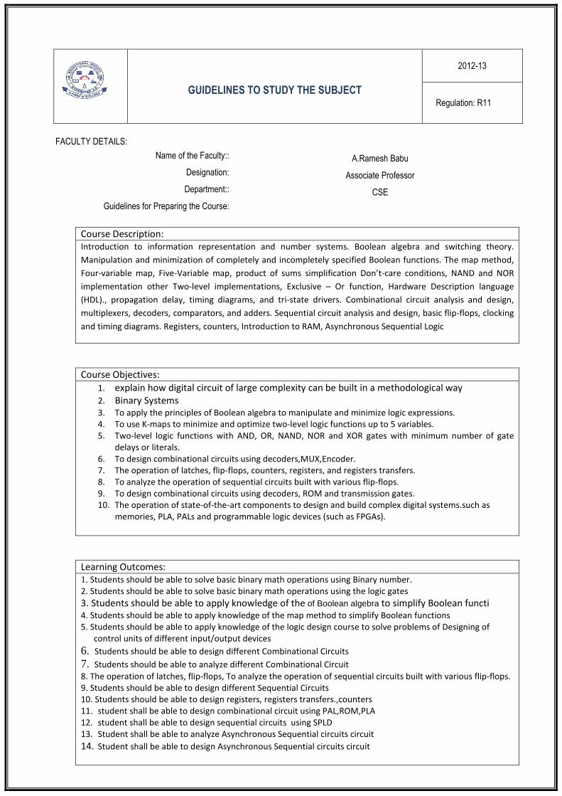
FACULTY DETAILS:
Name of the Faculty:: A.Ramesh Babu
Designation: Associate Professor
Department:: CSE
Guidelines for Preparing the Course:
Course Description:
Introduction to information representation and number systems. Boolean algebra and switching theory.
Manipulation and minimization of completely and incompletely specified Boolean functions. The map method,
Four-variable map, Five-Variable map, product of sums simplification Don’t-care conditions, NAND and NOR
implementation other Two-level implementations, Exclusive – Or function, Hardware Description language
(HDL)., propagation delay, timing diagrams, and tri-state drivers. Combinational circuit analysis and design,
multiplexers, decoders, comparators, and adders. Sequential circuit analysis and design, basic flip-flops, clocking
and timing diagrams. Registers, counters, Introduction to RAM, Asynchronous Sequential Logic
Course Objectives:
1. explain how digital circuit of large complexity can be built in a methodological way
2. Binary Systems
3. To apply the principles of Boolean algebra to manipulate and minimize logic expressions.
4. To use K-maps to minimize and optimize two-level logic functions up to 5 variables.
5. Two-level logic functions with AND, OR, NAND, NOR and XOR gates with minimum number of gate
delays or literals.
6. To design combinational circuits using decoders,MUX,Encoder.
7. The operation of latches, flip-flops, counters, registers, and registers transfers.
8. To analyze the operation of sequential circuits built with various flip-flops.
9. To design combinational circuits using decoders, ROM and transmission gates.
10. The operation of state-of-the-art components to design and build complex digital systems.such as
memories, PLA, PALs and programmable logic devices (such as FPGAs).
Learning Outcomes:
1. Students should be able to solve basic binary math operations using Binary number.
2. Students should be able to solve basic binary math operations using the logic gates
3. Students should be able to apply knowledge of the of Boolean algebra to simplify Boolean functi
4. Students should be able to apply knowledge of the map method to simplify Boolean functions
5. Students should be able to apply knowledge of the logic design course to solve problems of Designing of
control units of different input/output devices
6. Students should be able to design different Combinational Circuits 7. Students should be able to analyze different Combinational Circuit 8. The operation of latches, flip-flops, To analyze the operation of sequential circuits built with various flip-flops.
9. Students should be able to design different Sequential Circuits
10. Students should be able to design registers, registers transfers.,counters
11. student shall be able to design combinational circuit using PAL,ROM,PLA
12. student shall be able to design sequential circuits using SPLD
13. Student shall be able to analyze Asynchronous Sequential circuits circuit
14. Student shall be able to design Asynchronous Sequential circuits circuit
GUIDELINES TO STUDY THE SUBJECT
2012-13
Regulation: R11
FACULTY DETAILS: Name of the Faculty:: A.Ramesh Babu
Designation: Associate Professor Department:: CSE
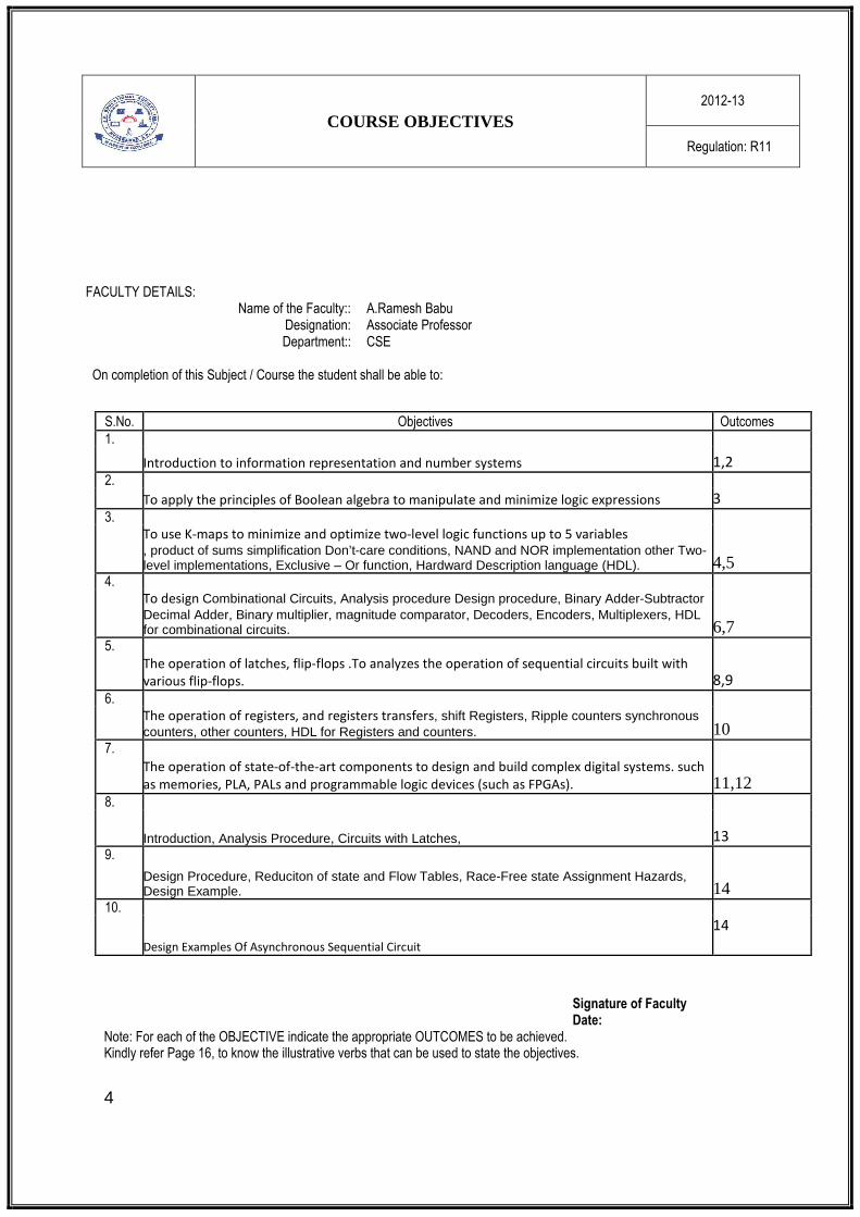
On completion of this Subject / Course the student shall be able to:
S.No. Objectives Outcomes 1.
Introduction to information representation and number systems 1,2 2.
To apply the principles of Boolean algebra to manipulate and minimize logic expressions 3 3.
To use K-maps to minimize and optimize two-level logic functions up to 5 variables
, product of sums simplification Don’t-care conditions, NAND and NOR implementation other Two-level implementations, Exclusive – Or function, Hardward Description language (HDL). 4,5
4.
To design Combinational Circuits, Analysis procedure Design procedure, Binary Adder-Subtractor Decimal Adder, Binary multiplier, magnitude comparator, Decoders, Encoders, Multiplexers, HDL for combinational circuits. 6,7
5.
The operation of latches, flip-flops .To analyzes the operation of sequential circuits built with
various flip-flops. 8,9 6.
The operation of registers, and registers transfers, shift Registers, Ripple counters synchronous counters, other counters, HDL for Registers and counters. 10
7.
The operation of state-of-the-art components to design and build complex digital systems. such
as memories, PLA, PALs and programmable logic devices (such as FPGAs). 11,12 8.
Introduction, Analysis Procedure, Circuits with Latches, 13 9.
Design Procedure, Reduciton of state and Flow Tables, Race-Free state Assignment Hazards, Design Example. 14
10.
Design Examples Of Asynchronous Sequential Circuit 14
Signature of Faculty Date:
Note: For each of the OBJECTIVE indicate the appropriate OUTCOMES to be achieved. Kindly refer Page 16, to know the illustrative verbs that can be used to state the objectives.
4
COURSE OBJECTIVES
2012-13
Regulation: R11
FACULTY DETAILS: Name of the Faculty:: A.Ramesh Babu
Designation: Associate Professor Department:: CSE
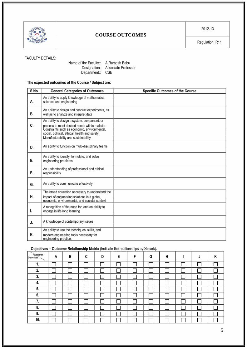
The expected outcomes of the Course / Subject are:
S.No. General Categories of Outcomes Specific Outcomes of the Course
A. An ability to apply knowledge of mathematics,
science, and engineering
B. An ability to design and conduct experiments, as
well as to analyze and interpret data
An ability to design a system, component, or
C. process to meet desired needs within realistic
Constraints such as economic, environmental,
social, political, ethical, health and safety,
Manufacturability and sustainability
D. An ability to function on multi-disciplinary teams
E. An ability to identify, formulate, and solve
engineering problems
F. An understanding of professional and ethical
responsibility
G. An ability to communicate effectively
The broad education necessary to understand the
H. impact of engineering solutions in a global,
economic, environmental, and societal context
I. A recognition of the need for, and an ability to
engage in life-long learning
J. A knowledge of contemporary issues
An ability to use the techniques, skills, and
K. modern engineering tools necessary for
engineering practice.
Objectives – Outcome Relationship Matrix (Indicate the relationships by�mark).
Outcomes A B C D E F G H I J K
Objectives
1.
2.
3.
4.
5.
6.
7.
8.
9.
10.
5
COURSE OUTCOMES
2012-13
Regulation: R11
FACULTY DETAILS:
Name of the Faculty:: A.Ramesh Babu Designation: Associate Professor
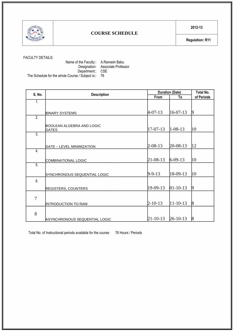
Department:: CSE The Schedule for the whole Course / Subject is:: 76
S. No. Description Duration (Date) Total No.
From To of Periods
1.
BINARY SYSTEMS 4-07-13 16-07-13 9
2.
BOOLEAN ALGEBRA AND LOGIC GATES 17-07-13 1-08-13 10
3.
GATE – LEVEL MINIMIZATION 2-08-13 20-08-13 12
4.
COMBINATIONAL LOGIC 21-08-13 6-09-13 10
5.
SYNCHRONOUS SEQUENTIAL LOGIC 9-9-13 18-09-13 10
6.
REGISTERS, COUNTERS 19-09-13 01-10-13 9
7 INTRODUCTION TO RAM 2-10-13 11-10-13
8
8 ASYNCHRONOUS SEQUENTIAL LOGIC 21-10-13 26-10-13 8
Total No. of Instructional periods available for the course: 76 Hours / Periods
COURSE SCHEDULE
2012-13
Regulation: R11
SCHEDULE OF INSTRUCTIONS
2012-13
UNIT - I Regulation: R11
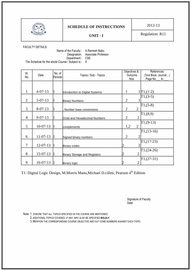
FACULTY DETAILS:
Name of the Faculty:: A.Ramesh Babu Designation: Associate Professor
Department:: CSE The Schedule for the whole Course / Subject is:: 9
SI. No. of Objectives & References
Date Topics / Sub - Topics
Outcome (Text Book, Journal…)
No. Periods
Nos. Page No___ to ___
1 4-07-13 1 Introduction to Digital Systems 1 1 T1,(1-2)
2 5-07-13 1 Binary Numbers 2 1 T1,(3-5)
3 8-07-13 1 , Number base conversions 2 2 T1,(5-8)
4 9-07-13 1 Octal and Hexadecimal Numbers 2 2 T1,(8,9)
5 10-07-13 1 complements 1,2 2 T1,(9-13)
6 11-07-13 1 Signed binary numbers 2 2
T1,(13-16)
7 12-07-13 1 Binary codes 2 2 T1,(17-23)
8 15-07-13 1 Binary Storage and Registers 2 2 T1,(24-26)
9 16-07-13 1 Binary logic 2 2 T1,(27-31)
T1: Digital Logic Design, M.Morris Mano,Michael D.cilleti, Pearson 4th Edition
Signature of Faculty Date
Note: 1. ENSURE THAT ALL TOPICS SPECIFIED IN THE COURSE ARE MENTIONED. 2. ADDITIONAL TOPICS COVERED, IF ANY, MAY ALSO BE SPECIFIED BOLDLY. 3. MENTION THE CORRESPONDING COURSE OBJECTIVE AND OUT COME NUMBERS AGAINST EACH TOPIC.
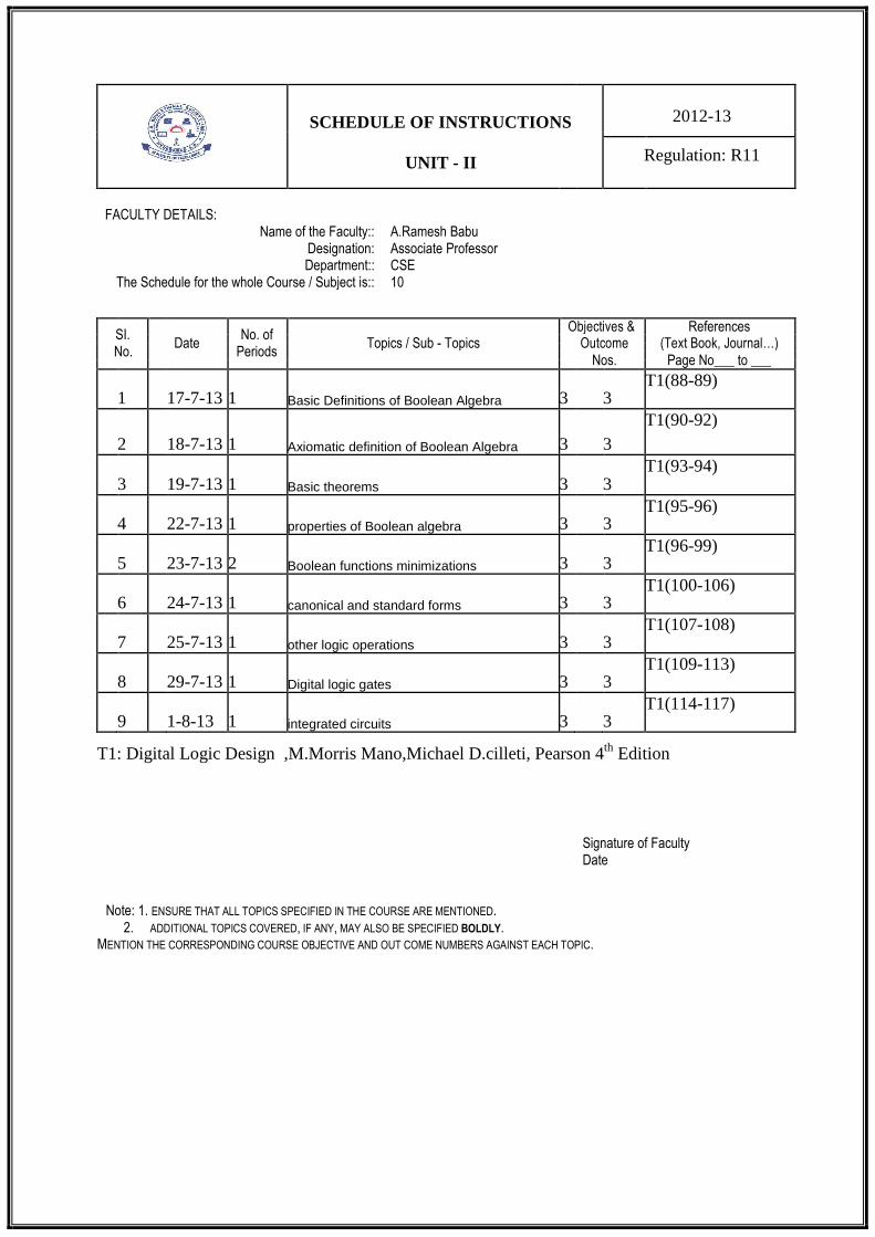
SCHEDULE OF INSTRUCTIONS
2012-13
UNIT - II Regulation: R11
FACULTY DETAILS:
Name of the Faculty:: A.Ramesh Babu Designation: Associate Professor
Department:: CSE The Schedule for the whole Course / Subject is:: 10
SI. No. of Objectives & References
Date Topics / Sub - Topics
Outcome (Text Book, Journal…)
No. Periods
Nos. Page No___ to ___
1 17-7-13 1 Basic Definitions of Boolean Algebra 3 3 T1(88-89)
2 18-7-13 1 Axiomatic definition of Boolean Algebra 3 3 T1(90-92)
3 19-7-13 1 Basic theorems 3 3 T1(93-94)
4 22-7-13 1 properties of Boolean algebra 3 3 T1(95-96)
5 23-7-13 2 Boolean functions minimizations 3 3 T1(96-99)
6 24-7-13 1 canonical and standard forms 3 3 T1(100-106)
7 25-7-13 1 other logic operations 3 3 T1(107-108)
8 29-7-13 1 Digital logic gates 3 3 T1(109-113)
9 1-8-13 1 integrated circuits 3 3 T1(114-117)
T1: Digital Logic Design ,M.Morris Mano,Michael D.cilleti, Pearson 4th Edition
Signature of Faculty Date
Note: 1. ENSURE THAT ALL TOPICS SPECIFIED IN THE COURSE ARE MENTIONED. 2. ADDITIONAL TOPICS COVERED, IF ANY, MAY ALSO BE SPECIFIED BOLDLY.
MENTION THE CORRESPONDING COURSE OBJECTIVE AND OUT COME NUMBERS AGAINST EACH TOPIC.
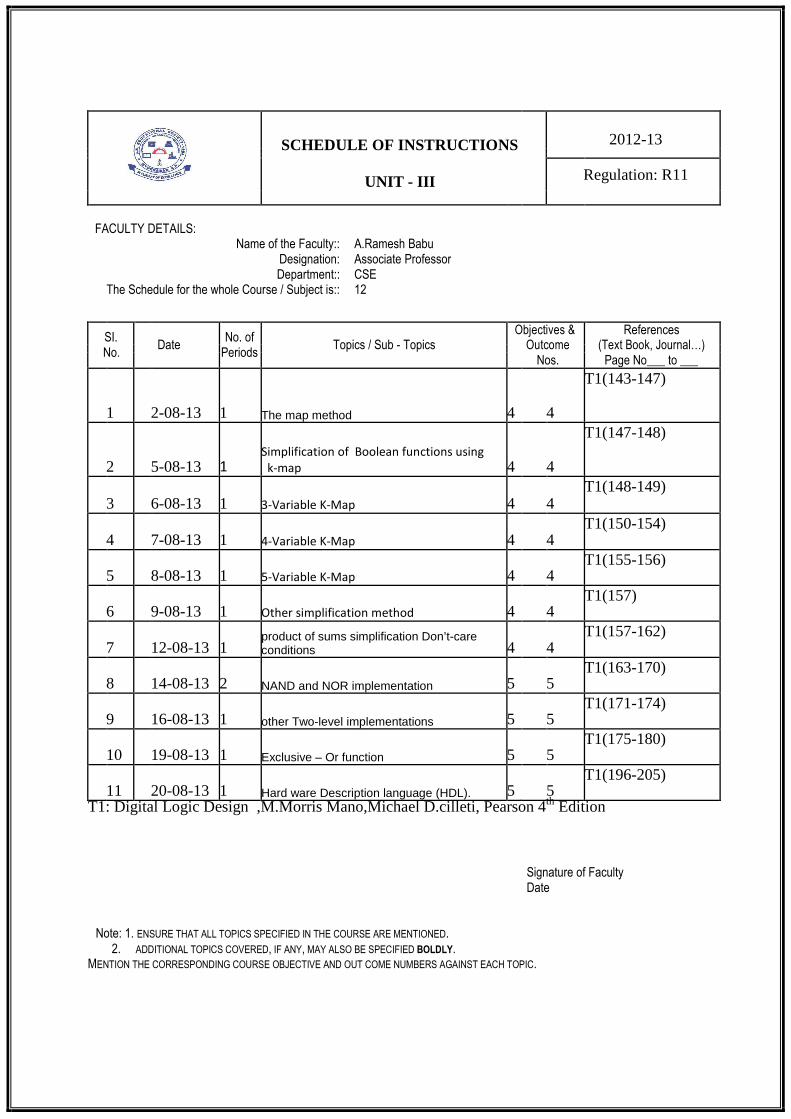
SCHEDULE OF INSTRUCTIONS
2012-13
UNIT - III Regulation: R11
FACULTY DETAILS:
Name of the Faculty:: A.Ramesh Babu Designation: Associate Professor
Department:: CSE The Schedule for the whole Course / Subject is:: 12
SI. No. of Objectives & References
Date Topics / Sub - Topics
Outcome (Text Book, Journal…)
No. Periods
Nos. Page No___ to ___
1 2-08-13 1 The map method 4 4
T1(143-147)
2 5-08-13 1 Simplification of Boolean functions using
k-map 4 4
T1(147-148)
3 6-08-13 1 3-Variable K-Map 4 4 T1(148-149)
4 7-08-13 1 4-Variable K-Map 4 4 T1(150-154)
5 8-08-13 1 5-Variable K-Map 4 4 T1(155-156)
6 9-08-13 1 Other simplification method 4 4 T1(157)
7 12-08-13 1 product of sums simplification Don’t-care conditions 4 4
T1(157-162)
8 14-08-13 2 NAND and NOR implementation 5 5 T1(163-170)
9 16-08-13 1 other Two-level implementations 5 5 T1(171-174)
10 19-08-13 1 Exclusive – Or function 5 5 T1(175-180)
11 20-08-13 1 Hard ware Description language (HDL). 5 5 T1(196-205)
T1: Digital Logic Design ,M.Morris Mano,Michael D.cilleti, Pearson 4th Edition
Signature of Faculty Date
Note: 1. ENSURE THAT ALL TOPICS SPECIFIED IN THE COURSE ARE MENTIONED. 2. ADDITIONAL TOPICS COVERED, IF ANY, MAY ALSO BE SPECIFIED BOLDLY.
MENTION THE CORRESPONDING COURSE OBJECTIVE AND OUT COME NUMBERS AGAINST EACH TOPIC.
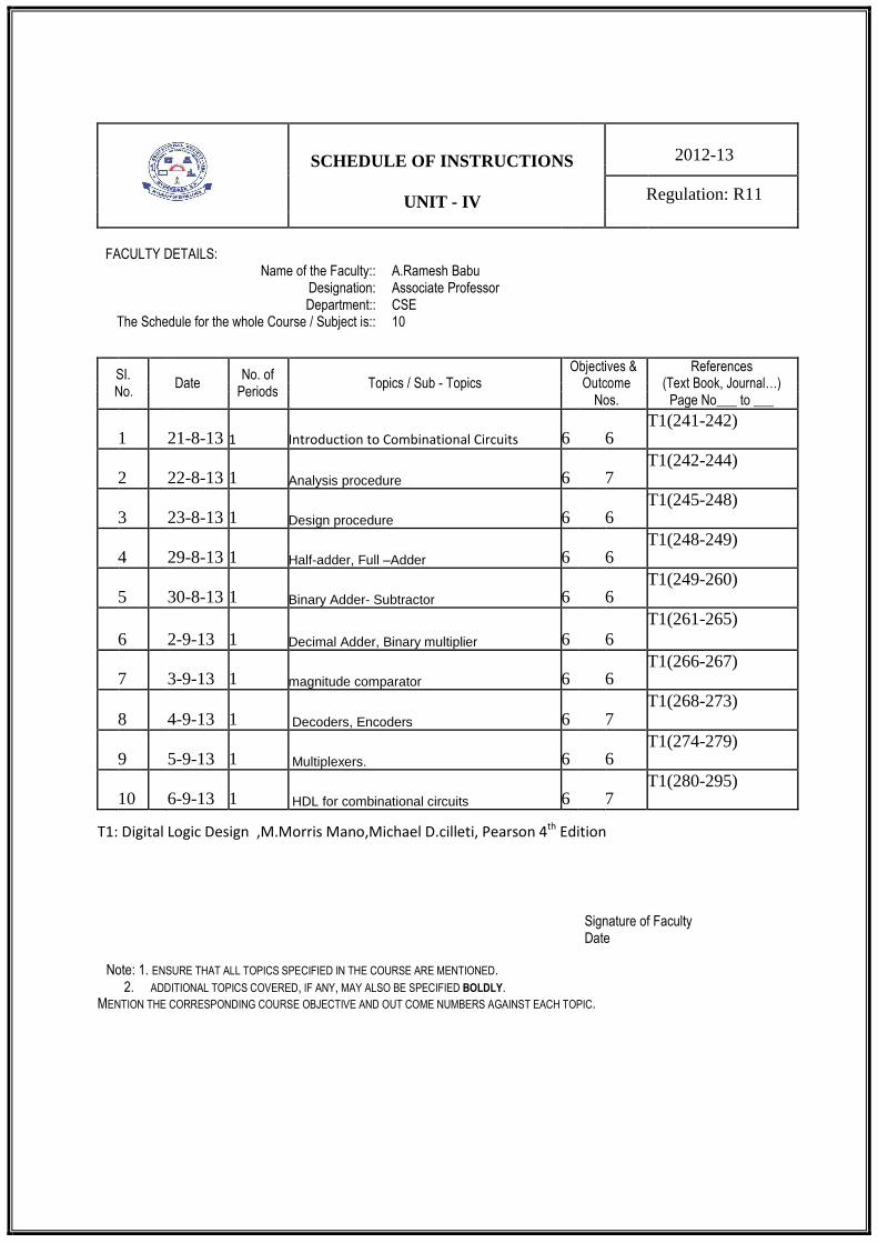
SCHEDULE OF INSTRUCTIONS
2012-13
UNIT - IV Regulation: R11
FACULTY DETAILS:
Name of the Faculty:: A.Ramesh Babu Designation: Associate Professor
Department:: CSE The Schedule for the whole Course / Subject is:: 10
SI. No. of Objectives & References
Date Topics / Sub - Topics
Outcome (Text Book, Journal…)
No. Periods
Nos. Page No___ to ___
1 21-8-13 1 Introduction to Combinational Circuits 6 6 T1(241-242)
2 22-8-13 1 Analysis procedure 6 7 T1(242-244)
3 23-8-13 1 Design procedure 6 6 T1(245-248)
4 29-8-13 1 Half-adder, Full –Adder 6 6 T1(248-249)
5 30-8-13 1 Binary Adder- Subtractor 6 6 T1(249-260)
6 2-9-13 1 Decimal Adder, Binary multiplier 6 6 T1(261-265)
7 3-9-13 1 magnitude comparator 6 6 T1(266-267)
8 4-9-13 1 Decoders, Encoders 6 7 T1(268-273)
9 5-9-13 1 Multiplexers. 6 6 T1(274-279)
10 6-9-13 1 HDL for combinational circuits 6 7 T1(280-295)
T1: Digital Logic Design ,M.Morris Mano,Michael D.cilleti, Pearson 4
th Edition
Signature of Faculty Date
Note: 1. ENSURE THAT ALL TOPICS SPECIFIED IN THE COURSE ARE MENTIONED.
2. ADDITIONAL TOPICS COVERED, IF ANY, MAY ALSO BE SPECIFIED BOLDLY. MENTION THE CORRESPONDING COURSE OBJECTIVE AND OUT COME NUMBERS AGAINST EACH TOPIC.
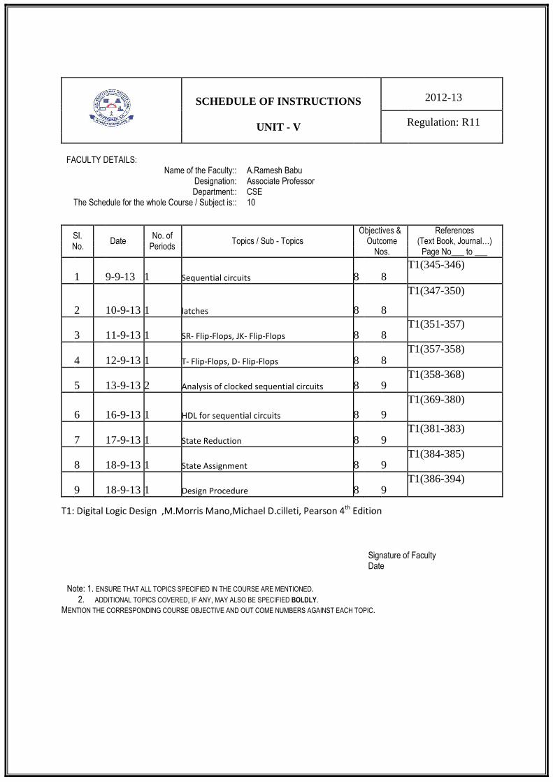
SCHEDULE OF INSTRUCTIONS
2012-13
UNIT - V Regulation: R11
FACULTY DETAILS:
Name of the Faculty:: A.Ramesh Babu Designation: Associate Professor
Department:: CSE The Schedule for the whole Course / Subject is:: 10
SI. No. of Objectives & References
Date Topics / Sub - Topics
Outcome (Text Book, Journal…)
No. Periods
Nos. Page No___ to ___
1 9-9-13 1 Sequential circuits 8 8 T1(345-346)
2 10-9-13 1 latches 8 8
T1(347-350)
3 11-9-13 1 SR- Flip-Flops, JK- Flip-Flops 8 8 T1(351-357)
4 12-9-13 1 T- Flip-Flops, D- Flip-Flops 8 8 T1(357-358)
5 13-9-13 2 Analysis of clocked sequential circuits 8 9 T1(358-368)
6 16-9-13 1 HDL for sequential circuits 8 9 T1(369-380)
7 17-9-13 1 State Reduction 8 9 T1(381-383)
8 18-9-13 1 State Assignment 8 9 T1(384-385)
9 18-9-13 1 Design Procedure 8 9 T1(386-394)
T1: Digital Logic Design ,M.Morris Mano,Michael D.cilleti, Pearson 4
th Edition
Signature of Faculty Date
Note: 1. ENSURE THAT ALL TOPICS SPECIFIED IN THE COURSE ARE MENTIONED.
2. ADDITIONAL TOPICS COVERED, IF ANY, MAY ALSO BE SPECIFIED BOLDLY. MENTION THE CORRESPONDING COURSE OBJECTIVE AND OUT COME NUMBERS AGAINST EACH TOPIC.
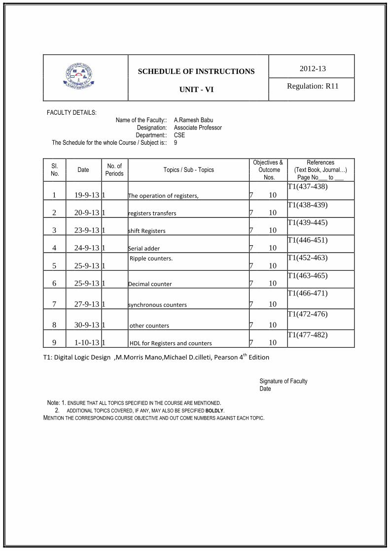
SCHEDULE OF INSTRUCTIONS
2012-13
UNIT - VI Regulation: R11
FACULTY DETAILS:
Name of the Faculty:: A.Ramesh Babu Designation: Associate Professor
Department:: CSE The Schedule for the whole Course / Subject is:: 9
SI. No. of Objectives & References
Date Topics / Sub - Topics
Outcome (Text Book, Journal…)
No. Periods
Nos. Page No___ to ___
1 19-9-13 1 The operation of registers, 7 10 T1(437-438)
2 20-9-13 1 registers transfers 7 10 T1(438-439)
3 23-9-13 1 shift Registers 7 10 T1(439-445)
4 24-9-13 1 Serial adder 7 10 T1(446-451)
5 25-9-13 1 Ripple counters.
7 10 T1(452-463)
6 25-9-13 1 Decimal counter 7 10 T1(463-465)
7 27-9-13 1 synchronous counters 7 10
T1(466-471)
8 30-9-13 1 other counters 7 10
T1(472-476)
9 1-10-13 1 HDL for Registers and counters 7 10 T1(477-482)
T1: Digital Logic Design ,M.Morris Mano,Michael D.cilleti, Pearson 4
th Edition
Signature of Faculty Date
Note: 1. ENSURE THAT ALL TOPICS SPECIFIED IN THE COURSE ARE MENTIONED.
2. ADDITIONAL TOPICS COVERED, IF ANY, MAY ALSO BE SPECIFIED BOLDLY. MENTION THE CORRESPONDING COURSE OBJECTIVE AND OUT COME NUMBERS AGAINST EACH TOPIC.
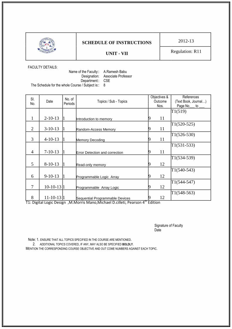
SCHEDULE OF INSTRUCTIONS
2012-13
UNIT - VII Regulation: R11
FACULTY DETAILS:
Name of the Faculty:: A.Ramesh Babu Designation: Associate Professor
Department:: CSE The Schedule for the whole Course / Subject is:: 8
SI. No. of Objectives & References
Date Topics / Sub - Topics
Outcome (Text Book, Journal…)
No. Periods
Nos. Page No___ to ___
1 2-10-13 1 Introduction to memory 9 11
T1(519)
2 3-10-13 1 Random-Access Memory 9 11 T1(520-525)
3 4-10-13 1 Memory Decoding 9 11 T1(526-530)
4 7-10-13 1 Error Detection and correction 9 11
T1(531-533)
5 8-10-13 1 Read-only memory 9 12 T1(534-539)
6 9-10-13 1 Programmable Logic Array 9 12 T1(540-543)
7 10-10-13 1 Programmable Array Logic 9 12 T1(544-547)
8 11-10-13 1 Sequential Programmable Devices 9 12 T1(548-563)
T1: Digital Logic Design ,M.Morris Mano,Michael D.cilleti, Pearson 4th
Edition
Signature of Faculty Date
Note: 1. ENSURE THAT ALL TOPICS SPECIFIED IN THE COURSE ARE MENTIONED.
2. ADDITIONAL TOPICS COVERED, IF ANY, MAY ALSO BE SPECIFIED BOLDLY. MENTION THE CORRESPONDING COURSE OBJECTIVE AND OUT COME NUMBERS AGAINST EACH TOPIC.
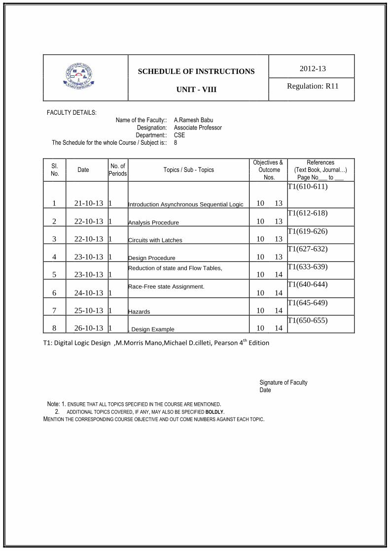
SCHEDULE OF INSTRUCTIONS
2012-13
UNIT - VIII Regulation: R11
FACULTY DETAILS:
Name of the Faculty:: A.Ramesh Babu Designation: Associate Professor
Department:: CSE The Schedule for the whole Course / Subject is:: 8
SI. No. of Objectives & References
Date Topics / Sub - Topics
Outcome (Text Book, Journal…)
No. Periods
Nos. Page No___ to ___
1 21-10-13 1 Introduction Asynchronous Sequential Logic 10 13
T1(610-611)
2 22-10-13 1 Analysis Procedure 10 13 T1(612-618)
3 22-10-13 1 Circuits with Latches 10 13 T1(619-626)
4 23-10-13 1 Design Procedure 10 13 T1(627-632)
5 23-10-13 1 Reduction of state and Flow Tables,
10 14 T1(633-639)
6 24-10-13 1 Race-Free state Assignment.
10 14 T1(640-644)
7 25-10-13 1 Hazards 10 14 T1(645-649)
8 26-10-13 1 , Design Example 10 14 T1(650-655)
T1: Digital Logic Design ,M.Morris Mano,Michael D.cilleti, Pearson 4
th Edition
Signature of Faculty Date
Note: 1. ENSURE THAT ALL TOPICS SPECIFIED IN THE COURSE ARE MENTIONED.
2. ADDITIONAL TOPICS COVERED, IF ANY, MAY ALSO BE SPECIFIED BOLDLY. MENTION THE CORRESPONDING COURSE OBJECTIVE AND OUT COME NUMBERS AGAINST EACH TOPIC.
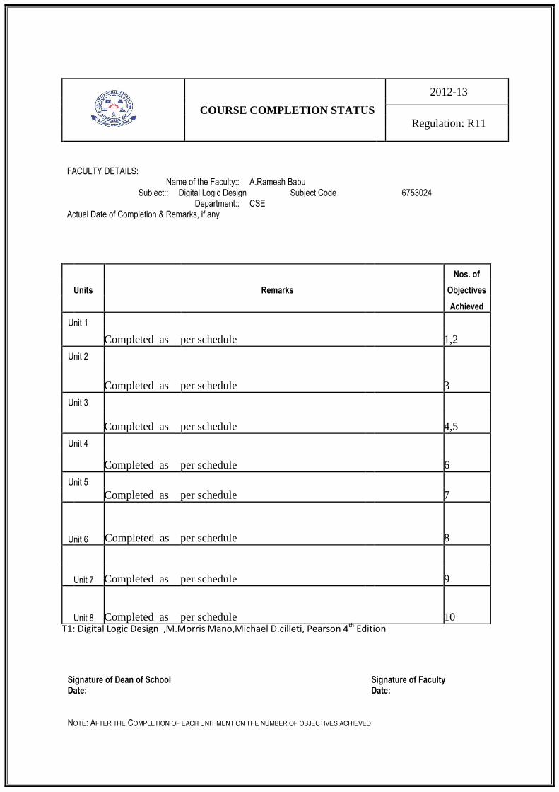
COURSE COMPLETION STATUS
2012-13
Regulation: R11
FACULTY DETAILS: Name of the Faculty:: A.Ramesh Babu
Subject:: Digital Logic Design Subject Code 6753024 Department:: CSE
Actual Date of Completion & Remarks, if any
Nos. of
Units Remarks Objectives
Achieved
Unit 1
Completed as per schedule 1,2
Unit 2
Completed as per schedule 3
Unit 3
Completed as per schedule 4,5
Unit 4
Completed as per schedule 6
Unit 5
Completed as per schedule 7
Unit 6 Completed as per schedule 8
Unit 7 Completed as per schedule 9
Unit 8 Completed as per schedule 10 T1: Digital Logic Design ,M.Morris Mano,Michael D.cilleti, Pearson 4
th Edition
Signature of Dean of School Signature of Faculty Date: Date:
NOTE: AFTER THE COMPLETION OF EACH UNIT MENTION THE NUMBER OF OBJECTIVES ACHIEVED.
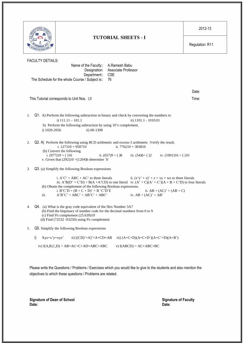
FACULTY DETAILS:
Name of the Faculty:: A.Ramesh Babu Designation: Associate Professor
Department:: CSE The Schedule for the whole Course / Subject is:: 76
Date:
This Tutorial corresponds to Unit Nos. I,II Time:
1. Q1. A) Perform the following subtraction in binary and check by converting the numbers to i) 111.11 – 101.1 ii) 1101.1 - 1010.01 b) Perform the following subtraction by using 10’s complement. i) 1020-2056 ii) 60-1308
2. Q2. A) Perform the following using BCD arithmetic and excess-3 arithmetic .Verify the result. i. 127310 + 958710 ii. 776210 + 383810 (b) Convert the following. i. (977)10 = ( )16 ii. (657)9 = ( )8 iii. (54)6= ( )2 iv. (1001)16 = ( )10
v. Given that (292)10 =(1204)b determine `b'
3. Q3. (a) Simplify the following Boolean expressions
i. A’C’ + ABC + AC’ to three literals ii. (x’y’ + z)’ + z + xy + wz to three literals iii. A’B(D’ + C’D) + B(A +A’CD) to one literal iv. (A’ + C)(A’ + C’)(A + B + C’D) to four literals
(b) Obtain the complement of the following Boolean expressions. i. B’C’D + (B + C + D)’ + B ’C’D’E ii. AB + (AC)’ + (AB + C)
iii. A’B’C’ + ABC’ + AB’C’ + ABC’ iv. AB + (AC)’ + AB’ 4. Q4. (a) What is the gray code equivalent of the Hex Number 3A7 (b) Find the biquinary of number code for the decimal numbers from 0 to 9
(c) Find 9's complement (25.639)10 (d) Find (72532 -03250) using 9's complement
5. Q5. Simplify the following Boolean expressions
i) Xyz+x’y+xyz’ ii) [(CD)’+A]’+A+CD+AB iii) (A+C+D)(A+C+ D’)(A+C’+D)(A+B’)
iv) f(A,B,C,D) = AB+AC+C+AD+ABC+ABC v) f(ABCD) = AC+ABC+BC
Please write the Questions / Problems / Exercises which you would like to give to the students and also mention the
objectives to which these questions / Problems are related.
Signature of Dean of School Signature of Faculty Date: Date:
TUTORIAL SHEETS - I
2012-13
Regulation: R11
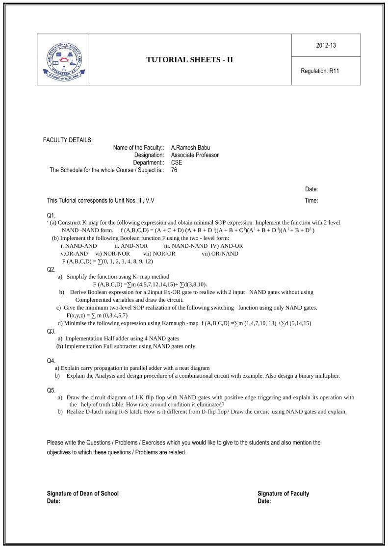
FACULTY DETAILS:
Name of the Faculty:: A.Ramesh Babu Designation: Associate Professor
Department:: CSE The Schedule for the whole Course / Subject is:: 76
Date:
This Tutorial corresponds to Unit Nos. III,IV,V Time:
Q1. . (a) Construct K-map for the following expression and obtain minimal SOP expression. Implement the function with 2-level NAND -NAND form. f (A,B,C,D) = (A + C + D) (A + B + D l)(A + B + C l)(A l + B + D l)(A l + B + Dl )
(b) Implement the following Boolean function F using the two - level form: i. NAND-AND ii. AND-NOR iii. NAND-NAND IV) AND-OR v.OR-AND vi) NOR-NOR vii) NOR-OR vii) OR-NAND F (A,B,C,D) = ∑(0, 1, 2, 3, 4, 8, 9, 12)
Q2. a) Simplify the function using K- map method
F (A,B,C,D) =∑m (4,5,7,12,14,15)+ ∑d(3,8,10). b) Derive Boolean expression for a 2input Ex-OR gate to realize with 2 input NAND gates without using
Complemented variables and draw the circuit. c) Give the minimum two-level SOP realization of the following switching function using only NAND gates.
F(x,y,z) = ∑ m (0,3,4,5,7) d) Minimise the following expression using Karnaugh -map f (A,B,C,D) =∑m (1,4,7,10, 13) +∑d (5,14,15)
Q3. a) Implementation Half adder using 4 NAND gates (b) Implementation Full subtracter using NAND gates only.
Q4. a) Explain carry propagation in parallel adder with a neat diagram b) Explain the Analysis and design procedure of a combinational circuit with example. Also design a binary multiplier.
Q5. a) Draw the circuit diagram of J-K flip flop with NAND gates with positive edge triggering and explain its operation with
the help of truth table. How race around condition is eliminated? b) Realize D-latch using R-S latch. How is it different from D-flip flop? Draw the circuit using NAND gates and explain.
Please write the Questions / Problems / Exercises which you would like to give to the students and also mention the
objectives to which these questions / Problems are related.
Signature of Dean of School Signature of Faculty Date: Date:
TUTORIAL SHEETS - II
2012-13
Regulation: R11
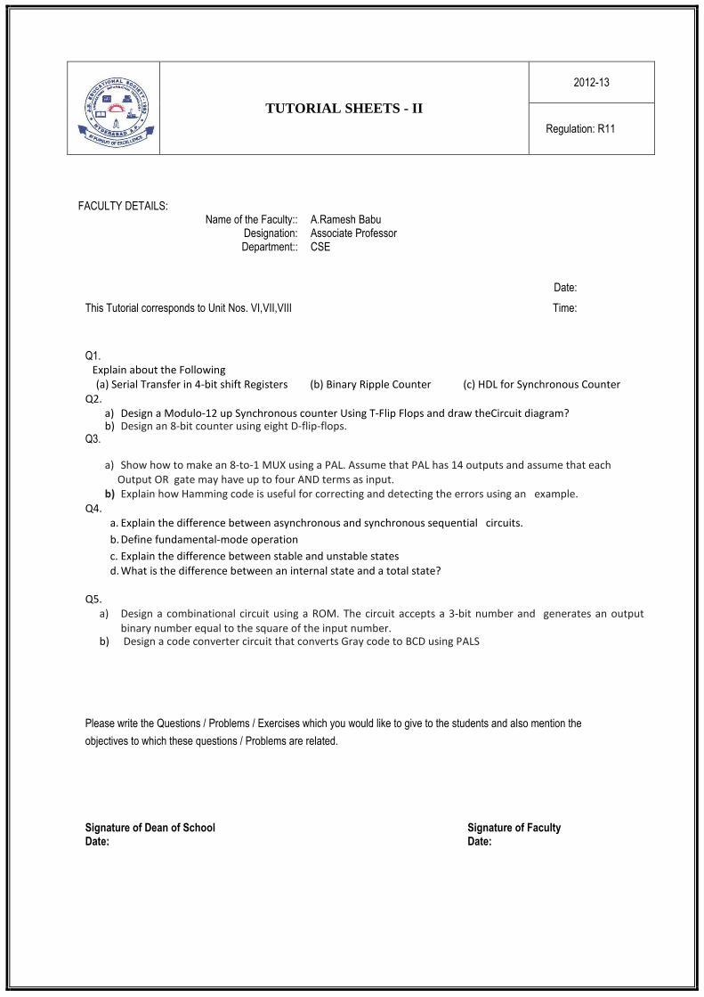
FACULTY DETAILS:
Name of the Faculty:: A.Ramesh Babu Designation: Associate Professor
Department:: CSE Date:
This Tutorial corresponds to Unit Nos. VI,VII,VIII Time:
Q1.
Explain about the Following
(a) Serial Transfer in 4-bit shift Registers (b) Binary Ripple Counter (c) HDL for Synchronous Counter
Q2.
a) Design a Modulo-12 up Synchronous counter Using T-Flip Flops and draw theCircuit diagram? b) Design an 8-bit counter using eight D-flip-flops.
Q3.
a) Show how to make an 8-to-1 MUX using a PAL. Assume that PAL has 14 outputs and assume that each
Output OR gate may have up to four AND terms as input.
b) Explain how Hamming code is useful for correcting and detecting the errors using an example.
Q4.
a. Explain the difference between asynchronous and synchronous sequential circuits.
b. Define fundamental-mode operation
c. Explain the difference between stable and unstable states
d. What is the difference between an internal state and a total state?
Q5.
a) Design a combinational circuit using a ROM. The circuit accepts a 3-bit number and generates an output
binary number equal to the square of the input number. b) Design a code converter circuit that converts Gray code to BCD using PALS
Please write the Questions / Problems / Exercises which you would like to give to the students and also mention the
objectives to which these questions / Problems are related.
Signature of Dean of School Signature of Faculty Date: Date:
TUTORIAL SHEETS - II
2012-13
Regulation: R11
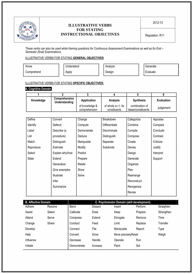
These verbs can also be used while framing questions for Continuous Assessment Examinations as well as for End – Semester (final) Examinations.
ILLUSTRATIVE VERBS FOR STATING GENERAL OBJECTIVES
Know Understand Analyze Generate
Comprehend Apply Design Evaluate
ILLUSTRATIVE VERBS FOR STATING SPECIFIC OBJECTIVES:
A. Cognitive Domain
1 2 3 4 5 6
Knowledge Comprehension
Application Analysis
Synthesis Evaluation
Understanding
of knowledge & of whole w.r.t. its combination of judgement
comprehension
constituents ideas/constituents
Define Convert Change Breakdown Categorize Appraise
Identify Defend Compute Differentiate Combine Compare
Label Describe (a Demonstrate Discriminate Compile Conclude
List procedure) Deduce Distinguish Compose Contrast
Match Distinguish Manipulate Separate Create Criticize
Reproduce Estimate Modify Subdivide Devise Justify
Select Explain why/how Predict Design Interpret
State Extend Prepare Generate Support
Generalize Relate Organize
Give examples Show Plan
Illustrate Solve Rearrange
Infer Reconstruct
Summarize Reorganize
Revise
B. Affective Domain C. Psychomotor Domain (skill development)
Adhere Resolve Bend Dissect Insert Perform Straighten
Assist Select Calibrate Draw Keep Prepare Strengthen
Attend Serve Compress Extend Elongate Remove Time
Change Share Conduct Feed Limit Replace Transfer
Develop Connect File Manipulate Report Type
Help Convert Grow Move preciselyReset Weigh
Influence Decrease Handle Operate Run
Initiate Demonstrate Increase Paint Set
ILLUSTRATIVE VERBS FOR STATING
INSTRUCTIONAL OBJECTIVES
2012-13
Regulation: R11
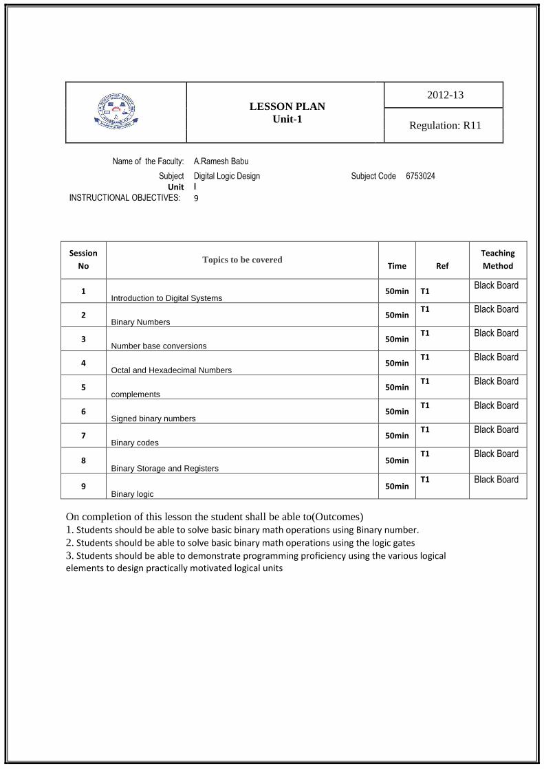
LESSON PLAN Unit-1
2012-13
Regulation: R11
Name of the Faculty: A.Ramesh Babu
Subject Digital Logic Design Subject Code 6753024
Unit I
INSTRUCTIONAL OBJECTIVES: 9
On completion of this lesson the student shall be able to(Outcomes) 1. Students should be able to solve basic binary math operations using Binary number. 2. Students should be able to solve basic binary math operations using the logic gates 3. Students should be able to demonstrate programming proficiency using the various logical
elements to design practically motivated logical units
Session
No Topics to be covered
Time
Ref
Teaching
Method
1 Introduction to Digital Systems
50min T1 Black Board
2 Binary Numbers
50min T1 Black Board
3 Number base conversions
50min T1 Black Board
4 Octal and Hexadecimal Numbers
50min T1 Black Board
5 complements
50min T1 Black Board
6 Signed binary numbers
50min T1 Black Board
7 Binary codes
50min T1 Black Board
8 Binary Storage and Registers
50min T1 Black Board
9 Binary logic
50min T1 Black Board
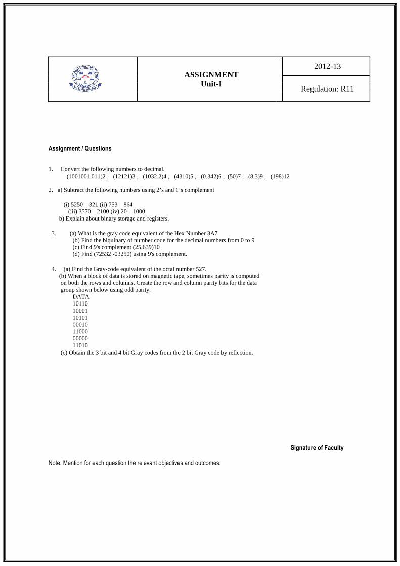
ASSIGNMENT Unit-I
2012-13
Regulation: R11
Assignment / Questions 1. Convert the following numbers to decimal. (1001001.011)2 , (12121)3 , (1032.2)4 , (4310)5 , (0.342)6 , (50)7 , (8.3)9 , (198)12 2. a) Subtract the following numbers using 2’s and 1’s complement
(i) 5250 – 321 (ii) 753 – 864 (iii) 3570 – 2100 (iv) 20 – 1000 b) Explain about binary storage and registers.
3. (a) What is the gray code equivalent of the Hex Number 3A7 (b) Find the biquinary of number code for the decimal numbers from 0 to 9
(c) Find 9's complement (25.639)10 (d) Find (72532 -03250) using 9's complement.
4. (a) Find the Gray-code equivalent of the octal number 527. (b) When a block of data is stored on magnetic tape, sometimes parity is computed on both the rows and columns. Create the row and column parity bits for the data group shown below using odd parity.
DATA 10110 10001 10101 00010 11000 00000 11010
(c) Obtain the 3 bit and 4 bit Gray codes from the 2 bit Gray code by reflection.
Signature of Faculty Note: Mention for each question the relevant objectives and outcomes.
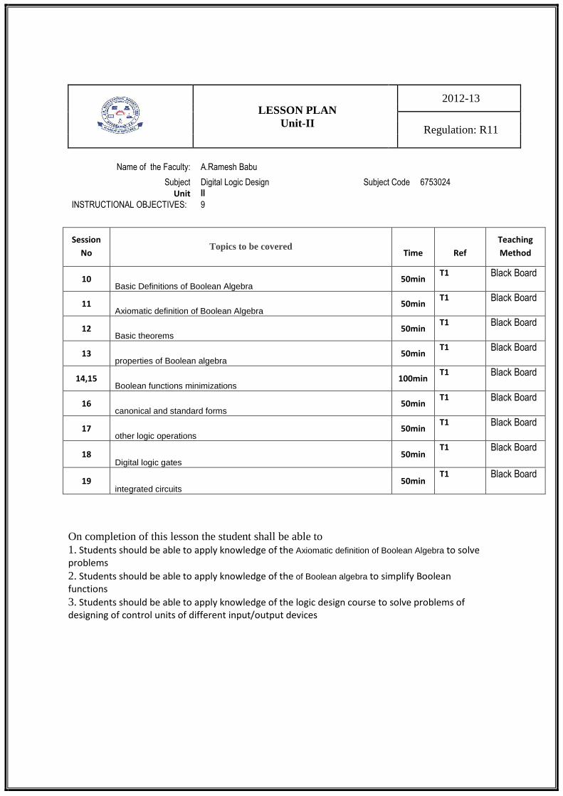
LESSON PLAN Unit-II
2012-13
Regulation: R11
Name of the Faculty: A.Ramesh Babu
Subject Digital Logic Design Subject Code 6753024
Unit II
INSTRUCTIONAL OBJECTIVES: 9
On completion of this lesson the student shall be able to 1. Students should be able to apply knowledge of the Axiomatic definition of Boolean Algebra to solve
problems 2. Students should be able to apply knowledge of the of Boolean algebra to simplify Boolean
functions 3. Students should be able to apply knowledge of the logic design course to solve problems of
designing of control units of different input/output devices
Session
No Topics to be covered
Time
Ref
Teaching
Method
10 Basic Definitions of Boolean Algebra
50min T1 Black Board
11 Axiomatic definition of Boolean Algebra
50min T1 Black Board
12 Basic theorems
50min T1 Black Board
13 properties of Boolean algebra
50min T1 Black Board
14,15 Boolean functions minimizations
100min T1 Black Board
16 canonical and standard forms
50min T1 Black Board
17 other logic operations
50min T1 Black Board
18 Digital logic gates
50min T1 Black Board
19 integrated circuits
50min T1 Black Board
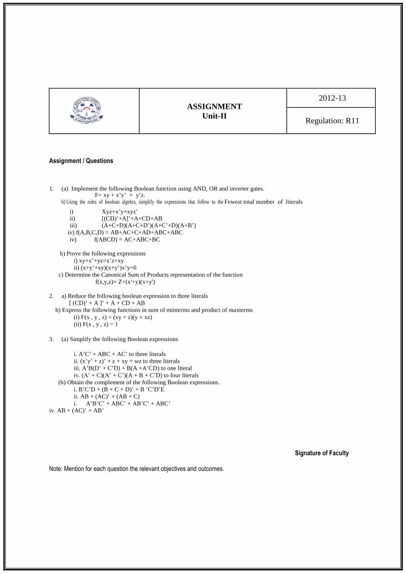
ASSIGNMENT Unit-II
2012-13
Regulation: R11
Assignment / Questions 1. (a) Implement the following Boolean function using AND, OR and inverter gates.
F= xy + x’y’ + y’z. b) Using the rules of boolean algebra, simplify the expressions that follow to the Fewest total number of literals
i) Xyz+x’y+xyz’ ii) [(CD)’+A]’+A+CD+AB iii) (A+C+D)(A+C+D’)(A+C’+D)(A+B’)
iv) f(A,B,C,D) = AB+AC+C+AD+ABC+ABC iv) f(ABCD) = AC+ABC+BC
b) Prove the following expressions
i) xy+x’+yz=x’z+xy ii) (x+y’+xy)(x+y’)x’y=0
c) Determine the Canonical Sum of Products representation of the function f(x,y,z)= Z+(x'+y)(x+y')
2. a) Reduce the following boolean expression to three literals [ (CD)’ + A ]’ + A + CD + AB b) Express the following functions in sum of minterms and product of maxterms
(i) F(x , y , z) = (xy + z)(y + xz) (ii) F(x , y , z) = 1
3. (a) Simplify the following Boolean expressions
i. A’C’ + ABC + AC’ to three literals ii. (x’y’ + z)’ + z + xy + wz to three literals iii. A’B(D’ + C’D) + B(A +A’CD) to one literal iv. (A’ + C)(A’ + C’)(A + B + C’D) to four literals
(b) Obtain the complement of the following Boolean expressions. i. B’C’D + (B + C + D)’ + B ’C’D’E ii. AB + (AC)’ + (AB + C) i. A’B’C’ + ABC’ + AB’C’ + ABC’
iv. AB + (AC)’ + AB’
Signature of Faculty Note: Mention for each question the relevant objectives and outcomes.

LESSON PLAN Unit-III
2012-13
Regulation: R11
Name of the Faculty: A.Ramesh Babu
Subject Digital Logic Design Subject Code 6753024
Unit III
INSTRUCTIONAL OBJECTIVES: 11
On completion of this lesson the student shall be able to(Outcomes) 1. Students should be able to apply knowledge of the map method to simplify Boolean functions 2. Students should be able to apply knowledge of the 3-variable k-map method to simplify Boolean
Functions 3. Students should be able to apply knowledge of the 4-variable k-map method to simplify Boolean
Functions Students should be able to apply knowledge of the logic design course to solve
problems of
Designing of control units of different input/output devices
Session
No Topics to be covered
Time
Ref
Teaching
Method
20 The map method
50min T1 Black Board
21 Simplification of Boolean functions using
k-map 50min
T1 Black Board
22 3-Variable K-Map
50min T1 Black Board
23 4-Variable K-Map
50min T1 Black Board
24 5-Variable K-Map
50min T1 Black Board
25 Other simplification method
50min T1 Black Board
26 product of sums simplification Don’t-care conditions
50min T1 Black Board
27,28 NAND and NOR implementation
100min T1 Black Board
29 other Two-level implementations
50min T1 Black Board
30 Exclusive – Or function
50min T1 Black Board
31 Hard ware Description language (HDL).
50min T1 Black Board
ASSIGNMENT Unit-III
2012-13
Regulation: R11
Assignment / Questions (a) Each of the following functions actually represents a set of four functions corresponding to the various assignments of the don?t care terms. f1 (w,x,y,z) = ∑(1,3,4,5,9,10, 11) + ∑φ(6,8) f2 (w,x,y,z) = ∑ (0,2,4,7,8,15) + ∑φ (9,12) then i. Find such that f3 = f1.f2 ii. Find such that f4 = f1 + f2 iii. Simplify and obtain minimal sop for f3 and f4. (b) Determine the canonical sum-of-products representation of the below . Functions i. f(x, y, z) = z + (x l + y)(x + y l ) ii. f(x, y, z) = x + (x l y l + x l z) 2.
(a) Construct K-map for the following expression and obtain minimal SOP ex- pression. Implement the function with 2-level NAND -NAND form. f (A,B,C,D) = (A + C + D) (A + B + D l)(A + B + C l)(A l + B + D l)(A l + B + Dl ) (b) Implement the following Boolean function F using the two - level form: i. NAND-AND ii. AND-NOR iii. NAND-NAND IV) AND-OR v.OR-AND vi) NOR-NOR vii) NOR-OR vii) OR-NAND F (A,B,C,D) = ∑(0, 1, 2, 3, 4, 8, 9, 12) 3. (a) If F1(A,B,C) = A Φ B Φ C F2 (A,B,C) = A Φ C Φ B Show that = F1 = F2 (b) Show that A Φ B Φ AB = A + B (c) Obtain minimal SOP expression for the complement of the given expression: F(A,B,C) = π(1, 2, 5, 7) And draw the circuit using NOR - gates. 4. Using the maps method, simplify the following expression using sum of the product from.
a) (abc)’+a(bc)’ +don’t cares abc+a’bc’+a’b’c
b) Abc+(ab)’c +don’t cares abc’+ab’c
Signature of Faculty
Note: Mention for each question the relevant objectives and outcomes.
LESSON PLAN Unit-IV
2012-13
Regulation: R11
Name of the Faculty: A.Ramesh Babu
Subject Digital Logic Design Subject Code 6753024
Unit IV
INSTRUCTIONAL OBJECTIVES: 10
On completion of this lesson the student shall be able to (Outcomes) 1. Students should be able to design different Combinational Circuits 2. Students should be able to analyze different Combinational Circuit 3. Students should be able to design Half-adder, Full –Adder, Binary Adder 4 Students should be able to design Decoders, Encoders, and Multiplexers.
Session
No Topics to be covered
Time
Ref
Teaching
Method
32 Introduction to Combinational Circuits
50min T1 Black Board
33 Analysis procedure
50min T1 Black Board
34 Design procedure
50min T1 Black Board
35 Half-adder, Full –Adder, Binary Adder
50min T1 Black Board
36 Binary Adder- Subtractor
50min T1 Black Board
37 Decimal Adder, Binary multiplier
50min T1 Black Board
38 magnitude comparator
50min T1 Black Board
39 Decoders, Encoders
50min T1 Black Board
40 Multiplexers.
50min T1 Black Board
41 HDL for combinational circuits
50min T1 Black Board
ASSIGNMENT Unit-IV
2012-13
Regulation: R11
Assignment / Questions (a) Implementation Half adder using 4 NAND gates (b) Implementation Full subtracter using NAND gates only. (a) Explain carry propagation in parallel adder with a neat diagram
c) Explain the Analysis and design procedure of a combinational circuit with example. Also design a binary multiplier.
Show how a 4 x 16 decoder can be constructed with two 3 x 8 decoders Show how a 16x1 MUX can be constructed with two 8x1 MUX
Signature of Faculty Note: Mention for each question the relevant objectives and outcomes.
LESSON PLAN Unit-V
2012-13
Regulation: R11
Name of the Faculty: A.Ramesh Babu
Subject Digital Logic Design Subject Code 6753024
Unit V
INSTRUCTIONAL OBJECTIVES: 9
On completion of this lesson the student shall be able to(Outcomes)
11. The operation of latches, flip-flops, To analyze the operation of sequential circuits built with
various flip-flops.
12. Students should be able to design different Sequential Circuits 13. Students should be able to design different Flip-Flops 14. Students should be able to Analyze of clocked sequential circuits
Session
No Topics to be covered
Time
Ref
Teaching
Method
42 Sequential circuits
50min T1 Black Board
43 latches
50min T1 Black Board
44 SR- Flip-Flops, JK- Flip-Flops
50min T1 Black Board
45 T- Flip-Flops, D- Flip-Flops
50min T1 Black Board
46,47 Analysis of clocked sequential circuits
100min T1 Black Board
48 HDL for sequential circuits
50min T1 Black Board
49 State Reduction
50min T1 Black Board
50 State Assignment
50min T1 Black Board
51 Design Procedure
50min T1 Black Board
ASSIGNMENT Unit-V
2012-13
Regulation: R11
Assignment / Questions
1. (a) Draw the circuit diagram of J-K flip flop with NAND gates with positive edge triggering and explain its operation with the help of truth table. How race around condition is eliminated? (b)Realize D-latch using R-S latch. How is it different from D-flip flop? Draw the circuit using NAND gates and explain.
2. A clocked sequential circuit is provided with a single input x and single output Z. Whenever the input produce a string of pulses 1 1 1 or 0 0 0 and at the end of the sequence it produce an output Z = 1 and overlapping is also allowed. (i) Obtain state-diagram (ii) Also obtain state-table (iii) Find equivalence classes using partition method and design the circuit using D-flip flops.
3. Design a sequential circuit with two D flip-flops A and B. and one input x. when x=0,the state of the circuit remains the same. When x=1,the circuit goes through
the state transition from 00 to 11 to 11 to 10 back to 00.and repeats
Signature of Faculty Note: Mention for each question the relevant objectives and outcomes.
LESSON PLAN Unit-VI
2012-13
Regulation: R11
Name of the Faculty: A.Ramesh Babu
Subject Digital Logic Design Subject Code 6753024
Unit VI
INSTRUCTIONAL OBJECTIVES: 9
On completion of this lesson the student shall be able to (Outcomes)
1. Students should be able to design registers, registers transfers.
2. Students should be able to design registers transfer
3. Students should be able to design counters,
Session
No Topics to be covered
Time
Ref
Teaching
Method
52 The operation of registers,
50min T1 Black Board
53 registers transfers
50min T1 Black Board
54 shift Registers
50min T1 Black Board
55 Serial adder
50min T1 Black Board
56 Ripple counters.
50min
T1 Black Board
57 Decimal counter
50min T1 Black Board
58 synchronous counters
50min T1 Black Board
59 other counters
50min T1 Black Board
60 HDL for Registers and counters
50min T1 Black Board
ASSIGNMENT Unit-VI
2012-13
Regulation: R11
Assignment / Questions
1. Design a Modulo-12 up Synchronous counter Using T-Flip Flops and draw the Circuit diagram?
2. (a) Construct a 4-bit universal shift register with multiplexers and explain the features with a neat schematic. (b)Write the HDL code for an Up-Down binary counter.
3. Design a modulo 16 counter.
4. Explain about the Following iv. Serial addition in 4-bit shift register
v. BCD Ripple Counter
(c) Universal Shift Register.
Signature of Faculty Note: Mention for each question the relevant objectives and outcomes.
LESSON PLAN Unit-VII
2012-13
Regulation: R11
Name of the Faculty: A.Ramesh Babu
Subject Digital Logic Design Subject Code 6753024
Unit VII
INSTRUCTIONAL OBJECTIVES: 8
On completion of this lesson the student shall be able to 1. Student shall be able to solve Error Detection and correction problems 2. Student shall be able to design combinational circuit using RAM 13. student shall be able to design combinational circuit using PROM
14. student shall be able to design combinational circuit using PLA 15. student shall be able to design combinational circuit using PAL 16. student shall be able to design sequential circuits using SPLD
Session
No Topics to be covered
Time
Ref
Teaching
Method
61 Introduction to memory
50min T1 Black Board
62 Random-Access Memory
50min T1 Black Board
63 Memory Decoding
50min T1 Black Board
64 Error Detection and correction
50min T1 Black Board
65 Read-only memory
50min T1 Black Board
66 Programmable Logic Array
50min T1 Black Board
67 Programmable Array Logic
50min T1 Black Board
68 Sequential Programmable Devices
50min T1 Black Board
ASSIGNMENT Unit-VII
2012-13
Regulation: R11
Assignment / Questions
1. Explain about PLA in Detail? 2. Explain the design of Sequential circuit with an example. Show the state reduction,
state assignment 3. Write notes on a)ROM b)RAM c)PLA d)PAL 4. (a) Design a combinational circuit using a ROM. The circuit accepts a 3-bit number
and generates an output binary number equal to the square of the input number. (b) Design a code converter circuit that converts Gray code to BCD using PALS.
Signature of Faculty Note: Mention for each question the relevant objectives and outcomes.
LESSON PLAN Unit-VIII
2012-13
Regulation: R11
Name of the Faculty: A.Ramesh Babu
Subject Digital Logic Design Subject Code 6753024
Unit VIII
INSTRUCTIONAL OBJECTIVES: 8
On completion of this lesson the student shall be able to 13. Student shall be able to analyze Asynchronous Sequential circuits circuit 14. Student shall be able to design Asynchronous Sequential circuits circuit 15. student shall be able to design latches 16. student shall be able to design Hazards 17. student shall be able to design Flow Tables
Session
No Topics to be covered
Time
Ref
Teaching
Method
69 Introduction Asynchronous Sequential Logic
50min T1
Black Board
70 Analysis Procedure
50min T1
Black Board
71 Circuits with Latches
50min T1
Black Board
72 Design Procedure
50min T1
Black Board
73 Reduction of state and Flow Tables, 50min T1
Black Board
74 Race-Free state Assignment. 50min T1
Black Board
75 Hazards
50min T1
Black Board
76 Design Example
50min T1
Black Board
ASSIGNMENT Unit-VIII
2012-13
Regulation: R11
Assignment / Questions 1. An Asynchronous sequential circuit is described by the following
excitation and output function. Y=x1x2’+(x1+x2’)y and Z=Y a. Draw the logic diagram of the circuit. b. Derive the transition table and output map. c. Obtain a 2-state flow table d. Describe in words the behaviour of the circuits
2. (a)Explain the types of Hazards in asynchronous sequential circuits. (b)Taking a suitable example, explain the elimination of essential hazards in a circuit.
3. Explain about the following: (a) latch excitation table (b) Merging of flow tables.
Signature of Faculty Note: Mention for each question the relevant objectives and outcomes.