Embed Size (px)
Citation preview
RF MEMs Variable Capacitors for Tunable Filters
Charles L. Goldsmith, Andrew Malczewski, Zhimin J. Yao, Shea Chen, John Ehmke,David H. Hinzel
Raytheon Systems Corporation, 13510 N. Central Expressway, MS 35 Dallas, Texas 75243
Recei ed 27 July 1998; re¨ised 30 December 1998
( )ABSTRACT: An RF MEMs microelectromechanical system variable capacitor has beendemonstrated with a 22:1 tuning range, tuning from 1.5 to 33.2 pF of capacitance. Thiscapacitor was constructed using bistable MEMs membrane capacitors with individualtuning ranges of 70:1 to 100:1, control voltages in the 30–55 V range, switching speeds lessthan 10 mS, and operating frequencies as high as 40 GHz. These devices may eventuallyprovide a viable alternative to electronic varactors with improved tuning range and lowerloss. Q 1999 John Wiley & Sons, Inc. Int J RF and Microwave CAE 9: 362]374, 1999.
Keywords: MEMs; microelectromechanical system; tunable capacitors varactors; membranecapacitor; tunable filter
I. INTRODUCTION
Variable capacitors are important control ele-ments in many high frequency radio receivers andtransmitters. The most common application of
Ž .tunable capacitors varactors in these radios is astunable filters and oscillators. Tunable circuitssuch as these commonly require a wide tuning
Ž .range and high quality factor high Q from thecontrol element. The advent of MEMs technologyfor RF applications enables new and excitingpossibilities for creating and controlling capaci-tance with wide tuning range and high Q. This isdue to the unique capabilities enabled by mi-cromechanical tuning and the low loss materialsused in the construction of RF MEMs devices.Several analog MEMs tuning methods have been
w xdemonstrated to date 1]4 . Unfortunately, thesedevices exhibited either a limited tuning range of
w xless than 2:1 1]3 or a very slow tuning schemew x4 . Modern receiver architectures require largetuning ranges and quick switching times. Thispaper presents a micromechanical capacitive tun-ing technique yielding bistable, digital capaci-
Correspondence to: C. Goldsmith
tance selection with tuning ranges greater than20:1 and tuning speeds on the order of micro-seconds.
II. MEMs CAPACITOR CONSTRUCTION
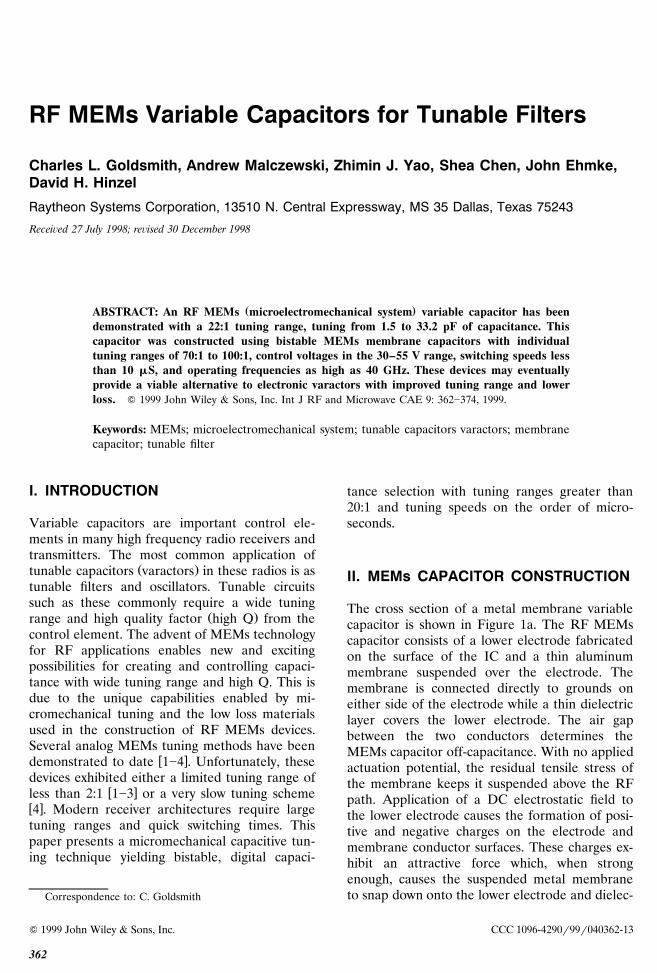
The cross section of a metal membrane variablecapacitor is shown in Figure 1a. The RF MEMscapacitor consists of a lower electrode fabricatedon the surface of the IC and a thin aluminummembrane suspended over the electrode. Themembrane is connected directly to grounds oneither side of the electrode while a thin dielectriclayer covers the lower electrode. The air gapbetween the two conductors determines theMEMs capacitor off-capacitance. With no appliedactuation potential, the residual tensile stress ofthe membrane keeps it suspended above the RFpath. Application of a DC electrostatic field tothe lower electrode causes the formation of posi-tive and negative charges on the electrode andmembrane conductor surfaces. These charges ex-hibit an attractive force which, when strongenough, causes the suspended metal membraneto snap down onto the lower electrode and dielec-
Q 1999 John Wiley & Sons, Inc. CCC 1096-4290r99r040362-13
362
RF MEMs Variable Capacitors for Filters 363
Figure 1. Cross-section of an RF MEMs capacitor inŽ . Ž .the unactuated a and actuated b positions.
tric surface, forming a low impedance RF path toground. Figure 1b demonstrates an RF MEMscapacitive capacitor in the actuated state. In thisstate, the characteristics of the dielectric layerprimarily determine the MEMs on-capacitance.By virtue of changing the position of the mem-brane with an applied DC voltage, the capaci-tance of this RF MEMs device can be changedover a significant capacitance range.
The RF MEMs capacitors described in thisarticle are built on high resistivity silicon sub-
Ž .strates ) 10 kV cm , with a 1 mm thick layer ofsilicon dioxide used as a buffer layer. The capaci-tor circuitry is fabricated on top of the silicondioxide using 4.0 mm thick aluminum intercon-nects which are compatible with CMOS circuitryand exhibit low conductor losses at high frequen-cies. The bottom electrode of the capacitors isbuilt using - 0.5 mm of refractory metal. Thisfilm provides good conductivity for low loss and
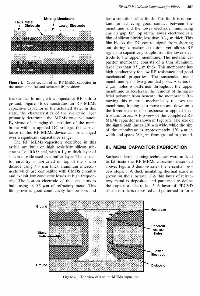
has a smooth surface finish. This finish is impor-tant for achieving good contact between themembrane and the lower electrode, minimizingany air gap. On top of the lower electrode is afilm of silicon nitride, less than 0.3 mm thick. Thisfilm blocks the DC control signal from shortingout during capacitor actuation, yet allows RFsignals to capacitively couple from the lower elec-trode to the upper membrane. The metallic ca-pacitor membrane consists of a thin aluminumlayer less than 0.5 mm thick. This membrane hashigh conductivity for low RF resistance and goodmechanical properties. The suspended metalmembrane spans two grounded posts. A series of2 mm holes is patterned throughout the uppermembrane to accelerate the removal of the sacri-ficial polymer from beneath the membrane. Re-moving this material mechanically releases themembrane, freeing it to move up and down ontothe lower electrode in response to applied elec-trostatic forces. A top view of the completed RFMEMs capacitor is shown in Figure 2. The size ofthe signal path line is 120 mm wide, while the sizeof the membrane is approximately 120 mm inwidth and spans 280 mm from ground to ground.
III. MEMs CAPACITOR FABRICATION
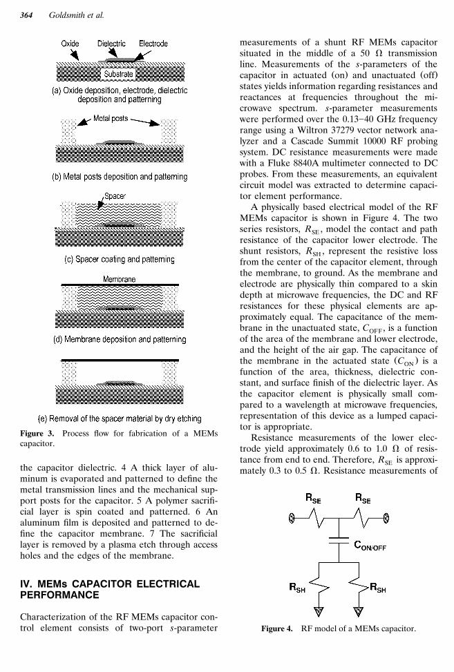
Surface micromachining techniques were utilizedto fabricate the RF MEMs capacitors describedabove. Figure 3 demonstrates the essential pro-cess steps: 1 A thick insulating thermal oxide isgrown on the substrate. 2 A thin layer of refrac-tory metal is deposited and patterned to definethe capacitor electrodes. 3 A layer of PECVDsilicon nitride is deposited and patterned to form
Figure 2. Top view of a shunt MEMs capacitor.
Goldsmith et al.364
Figure 3. Process flow for fabrication of a MEMscapacitor.
the capacitor dielectric. 4 A thick layer of alu-minum is evaporated and patterned to define themetal transmission lines and the mechanical sup-port posts for the capacitor. 5 A polymer sacrifi-cial layer is spin coated and patterned. 6 Analuminum film is deposited and patterned to de-fine the capacitor membrane. 7 The sacrificiallayer is removed by a plasma etch through accessholes and the edges of the membrane.
IV. MEMs CAPACITOR ELECTRICALPERFORMANCE
Characterization of the RF MEMs capacitor con-trol element consists of two-port s-parameter
measurements of a shunt RF MEMs capacitorsituated in the middle of a 50 V transmissionline. Measurements of the s-parameters of the
Ž . Ž .capacitor in actuated on and unactuated offstates yields information regarding resistances andreactances at frequencies throughout the mi-crowave spectrum. s-parameter measurementswere performed over the 0.13]40 GHz frequencyrange using a Wiltron 37279 vector network ana-lyzer and a Cascade Summit 10000 RF probingsystem. DC resistance measurements were madewith a Fluke 8840A multimeter connected to DCprobes. From these measurements, an equivalentcircuit model was extracted to determine capaci-tor element performance.
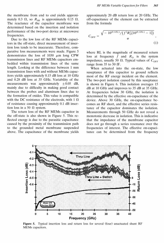
A physically based electrical model of the RFMEMs capacitor is shown in Figure 4. The twoseries resistors, R , model the contact and pathSEresistance of the capacitor lower electrode. Theshunt resistors, R , represent the resistive lossSHfrom the center of the capacitor element, throughthe membrane, to ground. As the membrane andelectrode are physically thin compared to a skindepth at microwave frequencies, the DC and RFresistances for these physical elements are ap-proximately equal. The capacitance of the mem-brane in the unactuated state, C , is a functionOFFof the area of the membrane and lower electrode,and the height of the air gap. The capacitance of
Ž .the membrane in the actuated state C is aONfunction of the area, thickness, dielectric con-stant, and surface finish of the dielectric layer. Asthe capacitor element is physically small com-pared to a wavelength at microwave frequencies,representation of this device as a lumped capaci-tor is appropriate.
Resistance measurements of the lower elec-trode yield approximately 0.6 to 1.0 V of resis-tance from end to end. Therefore, R is approxi-SEmately 0.3 to 0.5 V. Resistance measurements of
Figure 4. RF model of a MEMs capacitor.
RF MEMs Variable Capacitors for Filters 365
the membrane from end to end yields approxi-mately 0.3 V, so R is approximately 0.15 V.SHThe reactance of the capacitor membrane wasdetermined based on the insertion and isolationperformance of the two-port device at microwavefrequencies.
Due to the low loss of the RF MEMs capaci-tors in the off-state, direct measurement of inser-tion loss tends to be inaccurate. Therefore, com-parative loss measurements were made. Figure 5demonstrates the loss of 1030 mm long CPWtransmission lines and RF MEMs capacitors em-bedded within transmission lines of the samelength. Looking at the difference between 1 mmtransmission lines with and without MEMs capac-itors yields approximately 0.15 dB loss at 10 GHzand 0.28 dB loss at 35 GHz. Variability of themeasurements was approximately "0.05 dB,mainly due to difficulty in making good contactbetween the probes and aluminum lines due tothe formation of oxides. This value is compatiblewith the DC resistance of the electrode, with 1 Vof resistance causing approximately 0.1 dB inser-tion loss in a 50 V system.
The return loss of the RF MEMs capacitor inthe off-state is also shown in Figure 5. This re-flected energy is due to the parasitic capacitancecaused by the proximity of the transmission pathto the grounded metal membrane suspendedabove. The capacitance of the membrane yields
approximately 20 dB return loss at 20 GHz. Theoff-capacitance of the element can be extractedfrom the formula
Ž0.1 R L. 2 2 Ž0 .1 R L.w xy 10 r f R 10 y 1' Ž .OC s ,OFF p
Ž .1
where RL is the magnitude of measured returnloss at frequency f and R is the systemOimpedance, usually 50 V. Typical values of COFFrange from 35 to 50 fF.
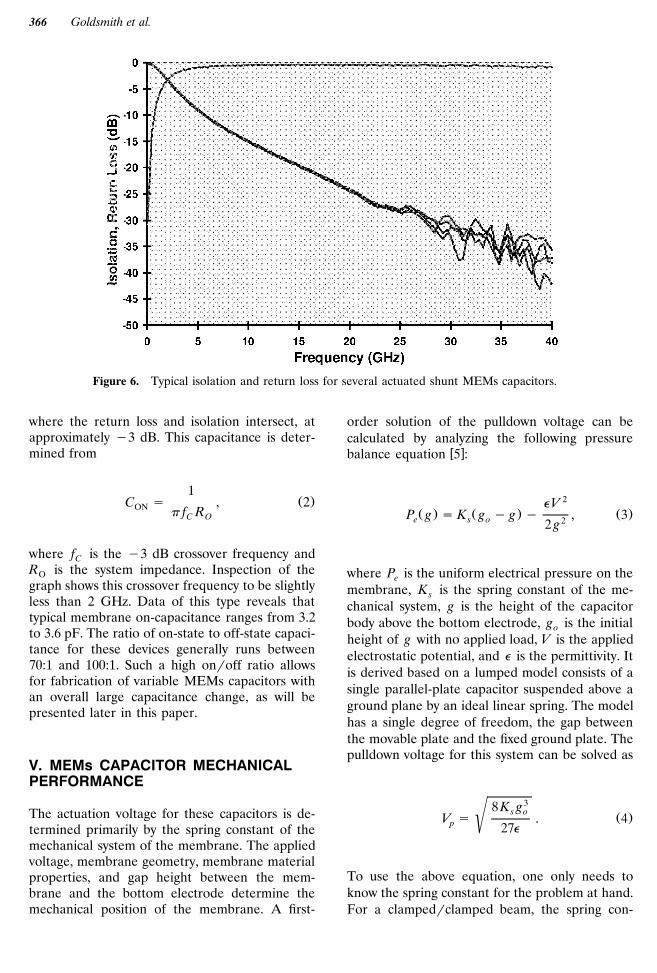
When actuated into the on-state, the lowsuseptance of this capacitor to ground reflectsmost of the RF energy incident on the element.The two-port isolation caused by this suseptanceis shown in Figure 6. This isolation averages 15dB at 10 GHz and improves to 35 dB at 35 GHz.At frequencies below 30 GHz, the isolation isdetermined by the effective on-capacitance of thedevice. Above 30 GHz, the on-capacitance be-comes an RF short, and the effective series resis-tance of the capacitor dominates the isolation.Measurements through 50 GHz do not reveal amonotonic decrease in isolation. This is indicativethat the impedance of the membrane capacitordoes not go through a series resonance over thefrequencies of interest. The effective on-capaci-tance can be determined from the frequency
Ž .Figure 5. Typical insertion loss and return loss for several four unactuated shunt RFMEMs capacitors.
Goldsmith et al.366
Figure 6. Typical isolation and return loss for several actuated shunt MEMs capacitors.
where the return loss and isolation intersect, atapproximately y3 dB. This capacitance is deter-mined from
1Ž .C s , 2ON p f RC O
where f is the y3 dB crossover frequency andCR is the system impedance. Inspection of theOgraph shows this crossover frequency to be slightlyless than 2 GHz. Data of this type reveals thattypical membrane on-capacitance ranges from 3.2to 3.6 pF. The ratio of on-state to off-state capaci-tance for these devices generally runs between70:1 and 100:1. Such a high onroff ratio allowsfor fabrication of variable MEMs capacitors withan overall large capacitance change, as will bepresented later in this paper.
V. MEMs CAPACITOR MECHANICALPERFORMANCE
The actuation voltage for these capacitors is de-termined primarily by the spring constant of themechanical system of the membrane. The appliedvoltage, membrane geometry, membrane materialproperties, and gap height between the mem-brane and the bottom electrode determine themechanical position of the membrane. A first-
order solution of the pulldown voltage can becalculated by analyzing the following pressure
w xbalance equation 5 :
eV 2
Ž . Ž . Ž .P g s K g y g y , 3e s o 22 g
where P is the uniform electrical pressure on thee
membrane, K is the spring constant of the me-s
chanical system, g is the height of the capacitorbody above the bottom electrode, g is the initialo
height of g with no applied load, V is the appliedelectrostatic potential, and e is the permittivity. Itis derived based on a lumped model consists of asingle parallel-plate capacitor suspended above aground plane by an ideal linear spring. The modelhas a single degree of freedom, the gap betweenthe movable plate and the fixed ground plate. Thepulldown voltage for this system can be solved as
38 K gs o Ž .V s . 4(p 27e
To use the above equation, one only needs toknow the spring constant for the problem at hand.For a clampedrclamped beam, the spring con-
RF MEMs Variable Capacitors for Filters 367
stant can be obtained by analyzing the associatedgoverning differential equation
d4 g d2 g eV 2 w˜ Ž .EI q s 1 y n wt s y q Pw.4 2 2dx dx 2 gŽ .5
w xThe result 5 is
˜ 3 Ž .32 Et 8s 1 y n tŽ .K s q , 6s 4 2L L
˜where E is the effective modulus, t is the beamthickness, L is the beam length, w is the beamwidth, s is the biaxial residual stress, n is thePoisson’s ratio, P is the pressure, and I is themoment of inertia with respect to the long axis of
˜the beam. For narrow beams E is the Young’smodulus E, while for wide beams
E˜ Ž .E s . 721 y n
Ž .The pulldown voltage predicated by eq. 4 couldbe significantly in error because the deformablecapacitor is represented by a rigid plate. Both theposition dependent electrostatic load and afirst-order fringing field correction term wereconsidered in an improved 2D distributed model.The governing equation is
d4 g d2 g˜ Ž .EI q s 1 y n wt4 2dx dx
eV 2 w gŽ .s y 1 q 0.65 . 82 ž /w2 g
The equation is nonlinear and was solved numeri-w xcally 6 . The closed-form expression for pulldown
voltage is
w Ž .x2.79 s 1 y nŽ .V s , 9P ( 2 w Ž .xeL D 1 q 0.42 g rwo
where
w Ž .x2 1 y cosh AD s 1 q Ž .A sinh A
and
12sŽ .A s 0.485L . 10( 3 3Et go
Ž .Though eq. 10 can be used directly for predic-tion of pulldown voltage it assumes that the bot-tom electrode has an area no less than the top
w xmembrane and has the following limitations 7 :
Ž .1 Structures must be nearly parallel.Ž .2 Structures must have a small gap to length
aspect ratio.Ž .3 Structures must have a good fixed bound-
ary condition.Ž .4 Gap must be small compared to the mem-
brane thickness.
For the RF MEMs capacitors described in thisŽ .article, not only is the gap ) 3 mm much larger
Ž .than the membrane thickness - 0.5 mm , butalso the effective area of the bottom electrode ismuch less than that of the membrane. In addi-tion, the movable electrode is not a rectangularmembrane and has a series of 2 mm holes pat-terned throughout it. These complexities necessi-tate that an accurate pulldown voltage be com-puted by use of a full 3D numerical simulation.
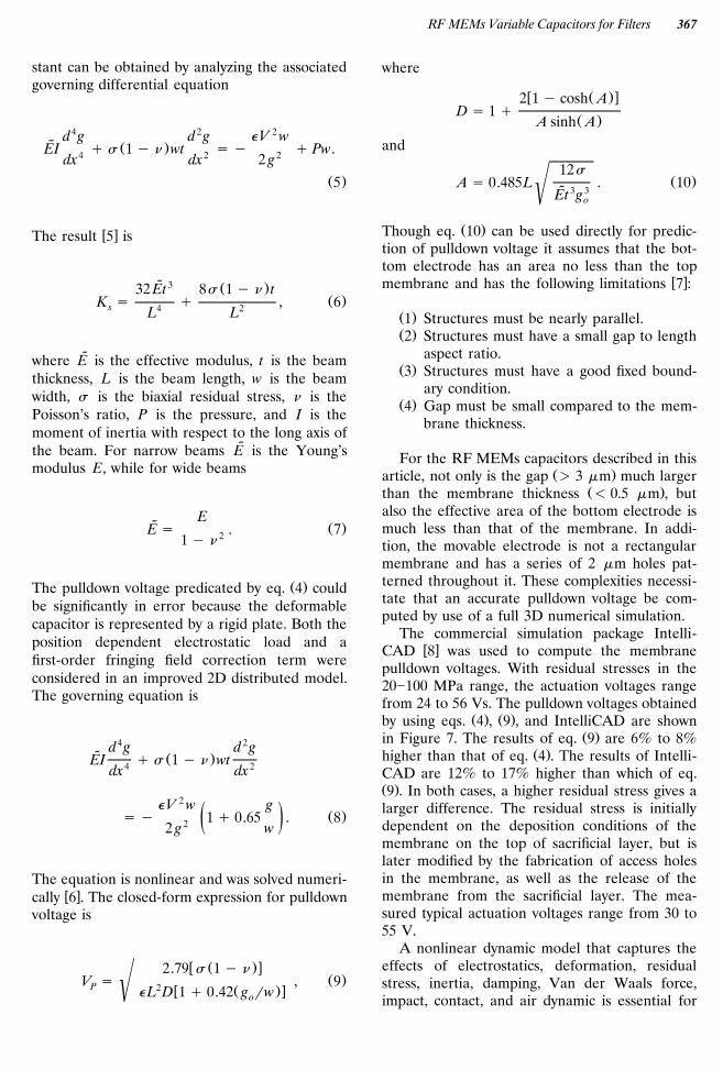
The commercial simulation package Intelli-w xCAD 8 was used to compute the membrane
pulldown voltages. With residual stresses in the20]100 MPa range, the actuation voltages rangefrom 24 to 56 Vs. The pulldown voltages obtained
Ž . Ž .by using eqs. 4 , 9 , and IntelliCAD are shownŽ .in Figure 7. The results of eq. 9 are 6% to 8%
Ž .higher than that of eq. 4 . The results of Intelli-CAD are 12% to 17% higher than which of eq.Ž .9 . In both cases, a higher residual stress gives alarger difference. The residual stress is initiallydependent on the deposition conditions of themembrane on the top of sacrificial layer, but islater modified by the fabrication of access holesin the membrane, as well as the release of themembrane from the sacrificial layer. The mea-sured typical actuation voltages range from 30 to55 V.
A nonlinear dynamic model that captures theeffects of electrostatics, deformation, residualstress, inertia, damping, Van der Waals force,impact, contact, and air dynamic is essential for
Goldsmith et al.368
Figure 7. Pulldown voltages vs. membrane residual stresses.
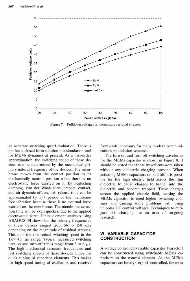
an accurate switching speed evaluation. There isneither a closed form solution nor simulation toolfor MEMs dynamics at present. As a first-orderapproximation, the switching speed of these de-vices can be determined by the mechanical pri-mary natural frequency of the devices. The mem-brane moves from the contact position to itsmechanically neutral position when there is noelectrostatic force exerted on it. By neglectingdamping, Van der Waals force, impact, contact,and air dynamic effects, this release time can beapproximated by 1r4 period of the membranefree vibration because there is no external forceexerted on the membrane. The membrane actua-tion time will be even quicker, due to the appliedelectrostatic force. Finite element analyses using
w xABAQUS 9 show that the primary frequenciesof these devices ranged from 56 to 150 kHzdepending on the magnitude of residual stresses.This puts the theoretical switching speed in the1.67]4.5 ms range. Typical measured switchingturn-on and turn-off times range from 3 to 6 ms.The high mechanical resonant frequencies andfast switching speeds of these devices allows forquick tuning of capacitor elements. This makesfor high speed tuning of oscillators and receiver
front-ends, necessary for many modern communi-cations modulation schemes.
The turn-on and turn-off switching waveformsfor the MEMs capacitor is shown in Figure 8. Itshould be noted that these waveforms were takenwithout any dielectric charging present. Whenactuating MEMs capacitors on and off, it is possi-ble for the high electric field across the thindielectric to cause charges to tunnel into thedielectric and become trapped. These chargesscreen the applied electric field, causing theMEMs capacitor to need higher switching volt-ages and causing some problems with usingunipolar DC control voltages. Techniques to miti-gate this charging are an area of on-goingresearch.
VI. VARIABLE CAPACITORCONSTRUCTION
Ž .A voltage controlled variable capacitor varactorcan be constructed using switchable MEMs ca-pacitors as the control element. As the MEMs
Ž .capacitors are binary onroff controlled, the most
RF MEMs Variable Capacitors for Filters 369
Figure 8. Typical switching speed measurements for aMEMs capacitor.
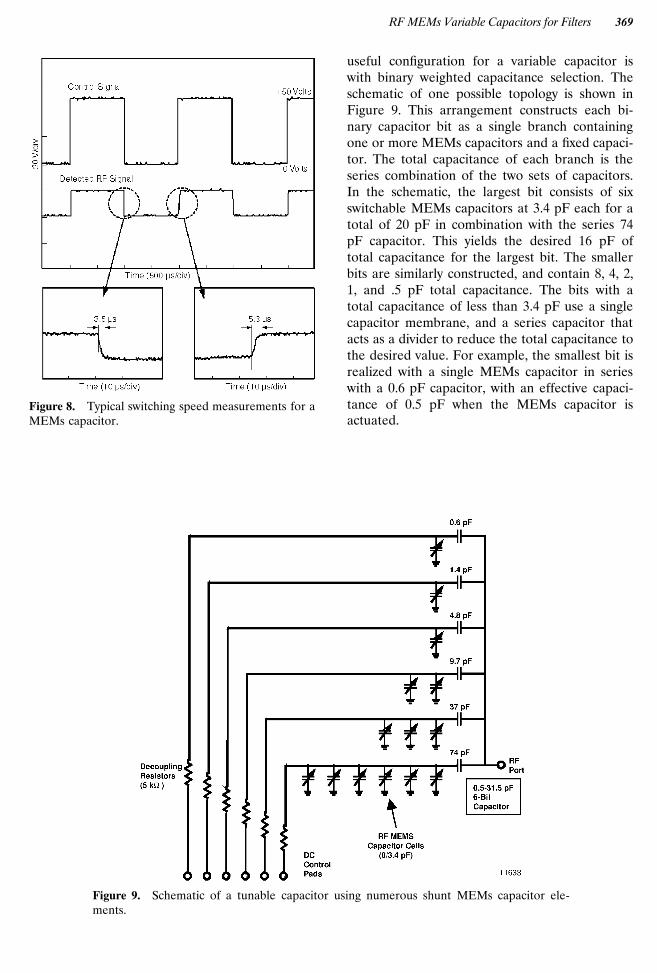
useful configuration for a variable capacitor iswith binary weighted capacitance selection. Theschematic of one possible topology is shown inFigure 9. This arrangement constructs each bi-nary capacitor bit as a single branch containingone or more MEMs capacitors and a fixed capaci-tor. The total capacitance of each branch is theseries combination of the two sets of capacitors.In the schematic, the largest bit consists of sixswitchable MEMs capacitors at 3.4 pF each for atotal of 20 pF in combination with the series 74pF capacitor. This yields the desired 16 pF oftotal capacitance for the largest bit. The smallerbits are similarly constructed, and contain 8, 4, 2,1, and .5 pF total capacitance. The bits with atotal capacitance of less than 3.4 pF use a singlecapacitor membrane, and a series capacitor thatacts as a divider to reduce the total capacitance tothe desired value. For example, the smallest bit isrealized with a single MEMs capacitor in serieswith a 0.6 pF capacitor, with an effective capaci-tance of 0.5 pF when the MEMs capacitor isactuated.
Figure 9. Schematic of a tunable capacitor using numerous shunt MEMs capacitor ele-ments.
Goldsmith et al.370
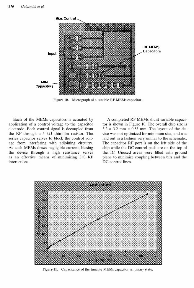
Figure 10. Micrograph of a tunable RF MEMs capacitor.
Each of the MEMs capacitors is actuated byapplication of a control voltage to the capacitorelectrode. Each control signal is decoupled fromthe RF through a 5 kV thin-film resistor. Theseries capacitor serves to block the control volt-age from interfering with adjoining circuitry.As each MEMs draws negligible current, biasingthe device through a high resistance servesas an effective means of minimizing DC]RFinteractions.
A completed RF MEMs shunt variable capaci-tor is shown in Figure 10. The overall chip size is3.2 = 3.2 mm = 0.53 mm. The layout of the de-vice was not optimized for minimum size, and waslaid out in a fashion very similar to the schematic.The capacitor RF port is on the left side of thechip while the DC control pads are on the top ofthe IC. Unused areas were filled with groundplane to minimize coupling between bits and theDC control lines.
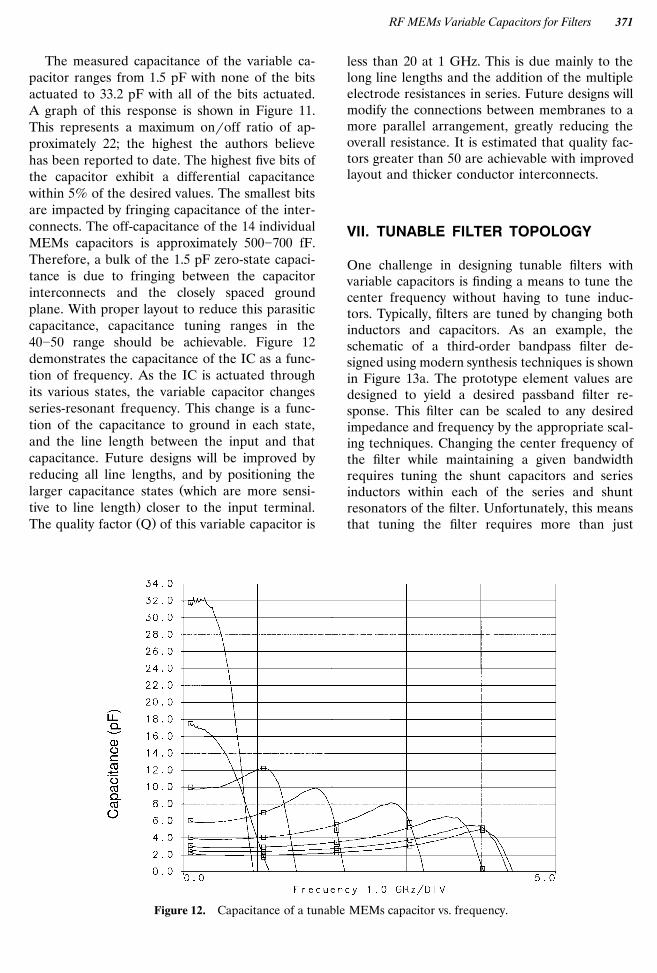
Figure 11. Capacitance of the tunable MEMs capacitor vs. binary state.
RF MEMs Variable Capacitors for Filters 371
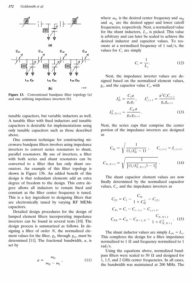
The measured capacitance of the variable ca-pacitor ranges from 1.5 pF with none of the bitsactuated to 33.2 pF with all of the bits actuated.A graph of this response is shown in Figure 11.This represents a maximum onroff ratio of ap-proximately 22; the highest the authors believehas been reported to date. The highest five bits ofthe capacitor exhibit a differential capacitancewithin 5% of the desired values. The smallest bitsare impacted by fringing capacitance of the inter-connects. The off-capacitance of the 14 individualMEMs capacitors is approximately 500]700 fF.Therefore, a bulk of the 1.5 pF zero-state capaci-tance is due to fringing between the capacitorinterconnects and the closely spaced groundplane. With proper layout to reduce this parasiticcapacitance, capacitance tuning ranges in the40]50 range should be achievable. Figure 12demonstrates the capacitance of the IC as a func-tion of frequency. As the IC is actuated throughits various states, the variable capacitor changesseries-resonant frequency. This change is a func-tion of the capacitance to ground in each state,and the line length between the input and thatcapacitance. Future designs will be improved byreducing all line lengths, and by positioning the
Žlarger capacitance states which are more sensi-.tive to line length closer to the input terminal.Ž .The quality factor Q of this variable capacitor is
less than 20 at 1 GHz. This is due mainly to thelong line lengths and the addition of the multipleelectrode resistances in series. Future designs willmodify the connections between membranes to amore parallel arrangement, greatly reducing theoverall resistance. It is estimated that quality fac-tors greater than 50 are achievable with improvedlayout and thicker conductor interconnects.
VII. TUNABLE FILTER TOPOLOGY
One challenge in designing tunable filters withvariable capacitors is finding a means to tune thecenter frequency without having to tune induc-tors. Typically, filters are tuned by changing bothinductors and capacitors. As an example, theschematic of a third-order bandpass filter de-signed using modern synthesis techniques is shownin Figure 13a. The prototype element values aredesigned to yield a desired passband filter re-sponse. This filter can be scaled to any desiredimpedance and frequency by the appropriate scal-ing techniques. Changing the center frequency ofthe filter while maintaining a given bandwidthrequires tuning the shunt capacitors and seriesinductors within each of the series and shuntresonators of the filter. Unfortunately, this meansthat tuning the filter requires more than just
Figure 12. Capacitance of a tunable MEMs capacitor vs. frequency.
Goldsmith et al.372
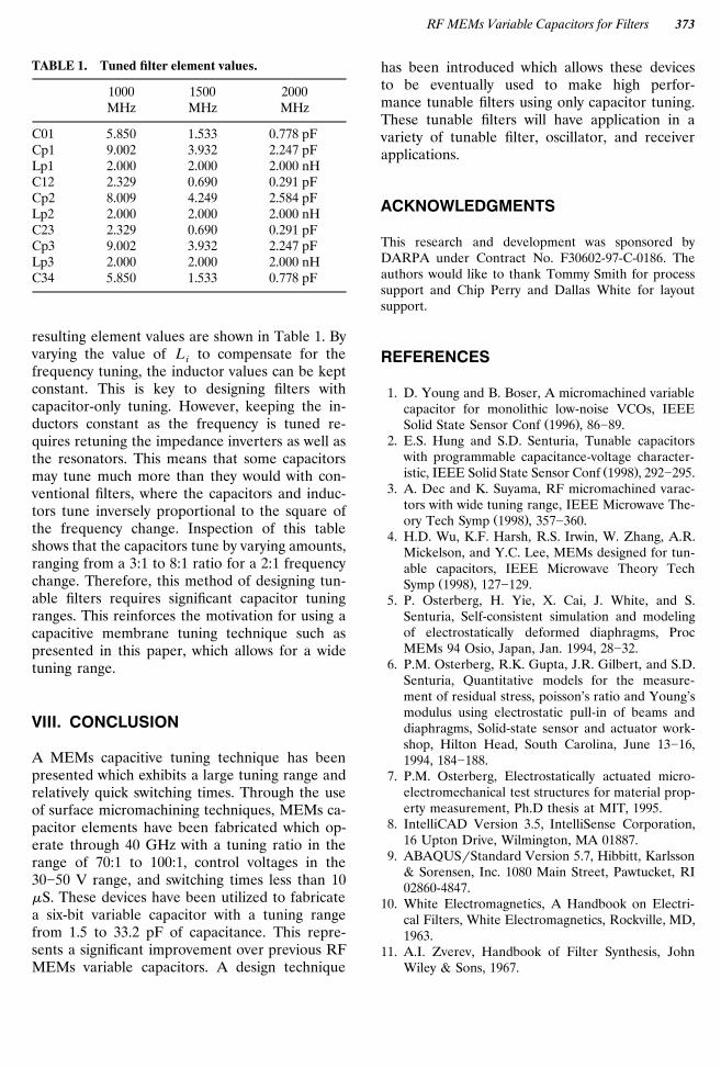
Ž .Figure 13. Conventional bandpass filter topology aŽ .and one utilizing impedance inverters b .
tunable capacitors, but variable inductors as well.A tunable filter with fixed inductors and tunablecapacitors is desirable for implementations usingonly tunable capacitors such as those describedabove.
One common technique for constructing mi-crowave bandpass filters involves using impedanceinverters to convert series resonators to shunt,parallel resonators. By use of inverters, a filterwith both series and shunt resonators can beconverted to a filter that has only shunt res-onators. An example of this filter topology isshown in Figure 13b. An added benefit of thisdesign is that redundant elements add an extradegree of freedom to the design. This extra de-gree allows all inductors to remain fixed andconstant as the filter center frequency is tuned.This is a key ingredient to designing filters thatare electronically tuned by varying RF MEMscapacitors.
Detailed design procedures for the design oflumped element filters incorporating impedance
w xinverters can be found in several texts 10 . Thedesign process is summarized as follows. In de-signing a filter of order N, the normalized ele-ment values for the filter, g through g , must be0 N
w xdetermined 11 . The fractional bandwidth, a, isset by
vO Ž .a s , 11v y vH L
where v is the desired center frequency and vO Hand v are the desired upper and lower cutoffLfrequencies, respectively. Next, a normalized valuefor the shunt inductors, L , is picked. This valueiis arbitrary and can later be scaled to achieve thedesired inductor and capacitor values. To res-onate at a normalized frequency of 1 radrs, thevalues for C are simplyi
1Ž .C s . 12i Li
Next, the impedance inverter values are de-signed based on the normalized element values,g , and the capacitor value C , withi i
C a a2 C C1 i iq12 2J s , J s01 i , iq1g g g g0 1 n nq1
C aN2 Ž .J s . 13N , Nq1 g gN Nq1
Next, the series caps that comprise the centerportion of the impedance inverters are designedas
1C s , C s J ,01 i , iq1 i , iq12(Ž .1rJ y 101
1Ž .C s . 14N , Nq1 2( Ž .1rJ y 1N , Nq1
The shunt capacitor element values are nowfinally determined by the normalized capacitorvalues, C , and the impedance inverters asi
C01C s C y y C ,P1 1 1221 q C01
C s C y C y C ,P i i iy1, i i , iq1
CN , Nq1 Ž .C s C y C y . 15PN N Ny1, N 21 q CN , Nq1
The shunt inductor values are simply L s L .P i iThis completes the design for a filter impedancenormalized to 1 V and frequency normalized to 1radrs.
Using the equations above, normalized band-pass filters were scaled to 50 V and designed for1, 1.5, and 2 GHz center frequencies. In all cases,the bandwidth was maintained at 200 MHz. The
RF MEMs Variable Capacitors for Filters 373
TABLE 1. Tuned filter element values.
1000 1500 2000MHz MHz MHz
C01 5.850 1.533 0.778 pFCp1 9.002 3.932 2.247 pFLp1 2.000 2.000 2.000 nHC12 2.329 0.690 0.291 pFCp2 8.009 4.249 2.584 pFLp2 2.000 2.000 2.000 nHC23 2.329 0.690 0.291 pFCp3 9.002 3.932 2.247 pFLp3 2.000 2.000 2.000 nHC34 5.850 1.533 0.778 pF
resulting element values are shown in Table 1. Byvarying the value of L to compensate for theifrequency tuning, the inductor values can be keptconstant. This is key to designing filters withcapacitor-only tuning. However, keeping the in-ductors constant as the frequency is tuned re-quires retuning the impedance inverters as well asthe resonators. This means that some capacitorsmay tune much more than they would with con-ventional filters, where the capacitors and induc-tors tune inversely proportional to the square ofthe frequency change. Inspection of this tableshows that the capacitors tune by varying amounts,ranging from a 3:1 to 8:1 ratio for a 2:1 frequencychange. Therefore, this method of designing tun-able filters requires significant capacitor tuningranges. This reinforces the motivation for using acapacitive membrane tuning technique such aspresented in this paper, which allows for a widetuning range.
VIII. CONCLUSION
A MEMs capacitive tuning technique has beenpresented which exhibits a large tuning range andrelatively quick switching times. Through the useof surface micromachining techniques, MEMs ca-pacitor elements have been fabricated which op-erate through 40 GHz with a tuning ratio in therange of 70:1 to 100:1, control voltages in the30]50 V range, and switching times less than 10mS. These devices have been utilized to fabricatea six-bit variable capacitor with a tuning rangefrom 1.5 to 33.2 pF of capacitance. This repre-sents a significant improvement over previous RFMEMs variable capacitors. A design technique
has been introduced which allows these devicesto be eventually used to make high perfor-mance tunable filters using only capacitor tuning.These tunable filters will have application in avariety of tunable filter, oscillator, and receiverapplications.
ACKNOWLEDGMENTS
This research and development was sponsored byDARPA under Contract No. F30602-97-C-0186. Theauthors would like to thank Tommy Smith for processsupport and Chip Perry and Dallas White for layoutsupport.
REFERENCES
1. D. Young and B. Boser, A micromachined variablecapacitor for monolithic low-noise VCOs, IEEE
Ž .Solid State Sensor Conf 1996 , 86]89.2. E.S. Hung and S.D. Senturia, Tunable capacitors
with programmable capacitance-voltage character-Ž .istic, IEEE Solid State Sensor Conf 1998 , 292]295.
3. A. Dec and K. Suyama, RF micromachined varac-tors with wide tuning range, IEEE Microwave The-
Ž .ory Tech Symp 1998 , 357]360.4. H.D. Wu, K.F. Harsh, R.S. Irwin, W. Zhang, A.R.
Mickelson, and Y.C. Lee, MEMs designed for tun-able capacitors, IEEE Microwave Theory Tech
Ž .Symp 1998 , 127]129.5. P. Osterberg, H. Yie, X. Cai, J. White, and S.
Senturia, Self-consistent simulation and modelingof electrostatically deformed diaphragms, ProcMEMs 94 Osio, Japan, Jan. 1994, 28]32.
6. P.M. Osterberg, R.K. Gupta, J.R. Gilbert, and S.D.Senturia, Quantitative models for the measure-ment of residual stress, poisson’s ratio and Young’smodulus using electrostatic pull-in of beams anddiaphragms, Solid-state sensor and actuator work-shop, Hilton Head, South Carolina, June 13]16,1994, 184]188.
7. P.M. Osterberg, Electrostatically actuated micro-electromechanical test structures for material prop-erty measurement, Ph.D thesis at MIT, 1995.
8. IntelliCAD Version 3.5, IntelliSense Corporation,16 Upton Drive, Wilmington, MA 01887.
9. ABAQUSrStandard Version 5.7, Hibbitt, Karlsson& Sorensen, Inc. 1080 Main Street, Pawtucket, RI02860-4847.
10. White Electromagnetics, A Handbook on Electri-cal Filters, White Electromagnetics, Rockville, MD,1963.
11. A.I. Zverev, Handbook of Filter Synthesis, JohnWiley & Sons, 1967.
Goldsmith et al.374
BIOGRAPHIES
Charles L. Goldsmith For bio and photo see p. 309.
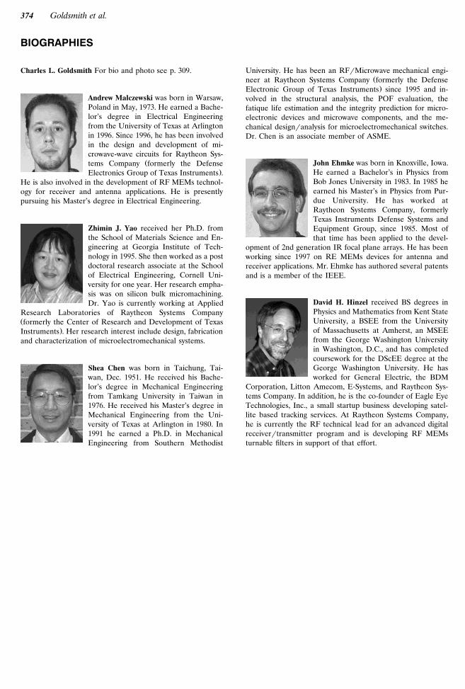
Andrew Malczewski was born in Warsaw,Poland in May, 1973. He earned a Bache-lor’s degree in Electrical Engineeringfrom the University of Texas at Arlingtonin 1996. Since 1996, he has been involvedin the design and development of mi-crowave-wave circuits for Raytheon Sys-
Žtems Company formerly the Defense.Electronics Group of Texas Instruments .
He is also involved in the development of RF MEMs technol-ogy for receiver and antenna applications. He is presentlypursuing his Master’s degree in Electrical Engineering.
Zhimin J. Yao received her Ph.D. fromthe School of Materials Science and En-gineering at Georgia Institute of Tech-nology in 1995. She then worked as a postdoctoral research associate at the Schoolof Electrical Engineering, Cornell Uni-versity for one year. Her research empha-sis was on silicon bulk micromachining.Dr. Yao is currently working at Applied
Research Laboratories of Raytheon Systems CompanyŽformerly the Center of Research and Development of Texas
.Instruments . Her research interest include design, fabricationand characterization of microelectromechanical systems.
Shea Chen was born in Taichung, Tai-wan, Dec. 1951. He received his Bache-lor’s degree in Mechanical Engineeringfrom Tamkang University in Taiwan in1976. He received his Master’s degree inMechanical Engineering from the Uni-versity of Texas at Arlington in 1980. In1991 he earned a Ph.D. in MechanicalEngineering from Southern Methodist
University. He has been an RFrMicrowave mechanical engi-Žneer at Raytheon Systems Company formerly the Defense.Electronic Group of Texas Instruments since 1995 and in-
volved in the structural analysis, the POF evaluation, thefatique life estimation and the integrity prediction for micro-electronic devices and microwave components, and the me-chanical designranalysis for microelectromechanical switches.Dr. Chen is an associate member of ASME.
John Ehmke was born in Knoxville, Iowa.He earned a Bachelor’s in Physics fromBob Jones University in 1983. In 1985 heearned his Master’s in Physics from Pur-due University. He has worked atRaytheon Systems Company, formerlyTexas Instruments Defense Systems andEquipment Group, since 1985. Most ofthat time has been applied to the devel-
opment of 2nd generation IR focal plane arrays. He has beenworking since 1997 on RE MEMs devices for antenna andreceiver applications. Mr. Ehmke has authored several patentsand is a member of the IEEE.
David H. Hinzel received BS degrees inPhysics and Mathematics from Kent StateUniversity, a BSEE from the Universityof Massachusetts at Amherst, an MSEEfrom the George Washington Universityin Washington, D.C., and has completedcoursework for the DScEE degree at theGeorge Washington University. He hasworked for General Electric, the BDM
Corporation, Litton Amecom, E-Systems, and Raytheon Sys-tems Company. In addition, he is the co-founder of Eagle EyeTechnologies, Inc., a small startup business developing satel-lite based tracking services. At Raytheon Systems Company,he is currently the RF technical lead for an advanced digitalreceiverrtransmitter program and is developing RF MEMsturnable filters in support of that effort.