Embed Size (px)
Citation preview
Section 24. Inter-Integrated Circuit™ (I2C™)
Inter-Integrated C
ircuit™ (I 2C
™)
24
HIGHLIGHTSThis section of the manual contains the following topics:
24.1 Overview..................................................................................................................24-224.2 Control and Status Registers...................................................................................24-424.3 I2C Bus Characteristics .........................................................................................24-1324.4 Enabling I2C Operation.......................................................................................... 24-1724.5 Communicating as a Master in a Single Master Environment ............................... 24-2024.6 Communicating as a Master in a Multi-Master Environment ................................. 24-3324.7 Communicating as a Slave....................................................................................24-3624.8 I2C Bus Connection Considerations ...................................................................... 24-5124.9 I2C Operation in Power-Saving Modes.................................................................. 24-5324.10 Effects of a Reset .................................................................................................. 24-5424.11 Pin Configuration In I2C Mode............................................................................... 24-5424.12 Related Application Notes ..................................................................................... 24-5524.13 Revision History.....................................................................................................24-56
© 2007-2011 Microchip Technology Inc. DS61116E-page 24-1
PIC32 Family Reference Manual
24.1 OVERVIEWThe Inter-Integrated Circuit™ (I2C™) module is a serial interface useful for communicating with other peripheral or microcontroller devices. These peripheral devices may be serial EEPROMs, display drivers, analog-to-digital converters, etc.
The I2C module can operate in any of the following I2C systems:
• As a slave device• As a master device in a single master system (slave may also be active)• As a master/slave device in a multi-master system (bus collision detection and arbitration
available)
The I2C module contains independent I2C master logic and I2C slave logic, each generating interrupts based on their events. In multi-master systems, the software is simply partitioned into a master controller and a slave controller.
When the I2C master logic is active, the slave logic also remains active, detecting the state of the bus and potentially receiving messages from itself in a single master system or from other masters in a multi-master system. No messages are lost during multi-master bus arbitration.
In a multi-master system, bus collision conflicts with other masters in the system are detected and reported to the application (BCOL interrupt). The software can terminate, and then restart the message transmission.
The I2C module contains a Baud Rate Generator (BRG). The I2C BRG does not consume other timer resources in the device.
Key features of the I2C module include the following:
• Independent master and slave logic• Multi-master support, which prevents message losses in arbitration• Detects 7-bit and 10-bit device addresses with configurable address masking in Slave
mode• Detects general call addresses as defined in the I2C protocol• Automatic SCLx clock stretching provides delays for the processor to respond to a slave
data request• Supports 100 kHz and 400 kHz bus specifications• Supports strict I2C reserved address rule
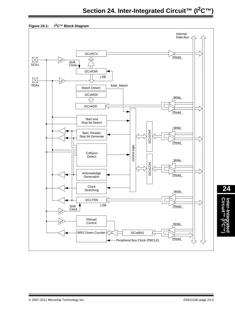
Figure 24-1 shows the I2C module block diagram.
Note: This family reference manual section is meant to serve as a complement to device data sheets. Depending on the device variant, this manual section may not apply to all PIC32 devices.
Please consult the note at the beginning of the “Inter-Integrated Circuit™ (I2C™)”chapter in the current device data sheet to check whether this document supports the device you are using.
Device data sheets and family reference manual sections are available for download from the Microchip Worldwide Web site at: http://www.microchip.com
DS61116E-page 24-2 © 2007-2011 Microchip Technology Inc.
Section 24. Inter-Integrated Circuit™ (I2C™)Inter-Integrated C
ircuit™ (I 2C
™)
24
Figure 24-1: I2C™ Block Diagram
I2CxRSR
I2CxRCV
InternalData Bus
SCKx
SDAx
Shift
Match Detect
I2CxADD
Start andStop bit Detect
Clock
Addr_Match
ClockStretching
I2CxTRNLSBShift
Clock
Write
Read
BRG Down Counter I2CxBRG
ReloadControl
Peripheral Bus Clock (PBCLK)
Start, Restart,Stop bit Generate
Write
Read
AcknowledgeGeneration
CollisionDetect
Write
Read
Write
ReadI2C
xCO
N
Write
ReadI2C
xSTA
T
cont
rol l
ogic
Read
LSB
I2CxMSK
© 2007-2011 Microchip Technology Inc. DS61116E-page 24-3
PIC32 Family Reference Manual
24.2 CONTROL AND STATUS REGISTERS
The I2C module consists of the following Special Function Registers (SFRs):
• I2CxCON: I2C™ Control RegisterThis register enables control of the I2C module’s operation.
• I2CxSTAT: I2C™ Status RegisterThis register contains status flags indicating the I2C module’s state during operation.
• I2CxADD: I2C™ Slave Address RegisterThis register holds the slave device address.
• I2CxMSK: I2C™ Address Mask RegisterThis register designates which bit positions in the I2CxADD register can be ignored, which allows for multiple address support.
• I2CxBRG: I2C™ Baud Rate Generator RegisterThis register holds the Baud Rate Generator (BRG) reload value for the I2C module Baud Rate Generator.
• I2CxTRN: I2C™ Transmit Data RegisterThis read-only register is the transmit register. Bytes are written to this register during a transmit operation.
• I2CxRCV: I2C™ Receive Data RegisterThis read-only register is the buffer register from which data bytes can be read.
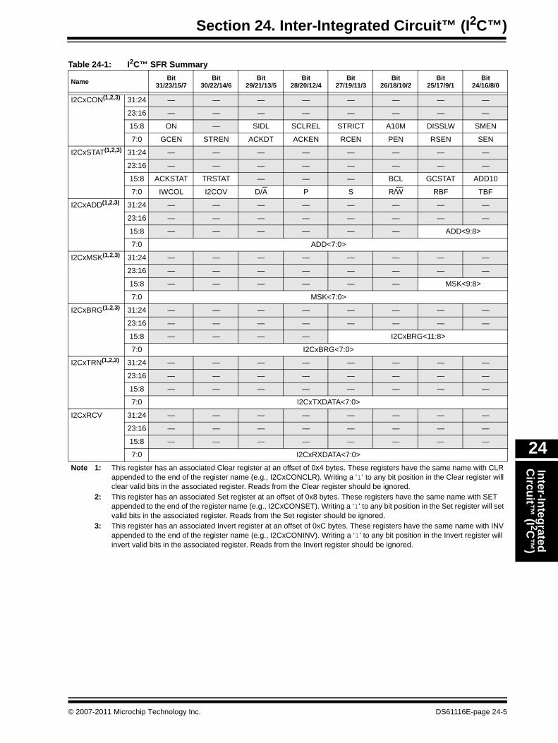
Table 24-1 summarizes all registers related to the I2C module. Corresponding registers appear after the summary, which include detailed bit descriptions for each register.
Note: Each PIC32 family device may have one or more I2C modules. An ‘x’ used in the names of pins, Control/Status bits, and registers denotes the particular module. Refer to the specific device data sheets for more details.
DS61116E-page 24-4 © 2007-2011 Microchip Technology Inc.
Section 24. Inter-Integrated Circuit™ (I2C™)Inter-Integrated C
ircuit™ (I 2C
™)
24
Table 24-1: I2C™ SFR Summary
Name Bit31/23/15/7
Bit30/22/14/6
Bit29/21/13/5
Bit28/20/12/4
Bit27/19/11/3
Bit26/18/10/2
Bit25/17/9/1
Bit24/16/8/0
I2CxCON(1,2,3) 31:24 — — — — — — — —
23:16 — — — — — — — —
15:8 ON — SIDL SCLREL STRICT A10M DISSLW SMEN
7:0 GCEN STREN ACKDT ACKEN RCEN PEN RSEN SEN
I2CxSTAT(1,2,3) 31:24 — — — — — — — —
23:16 — — — — — — — —
15:8 ACKSTAT TRSTAT — — — BCL GCSTAT ADD10
7:0 IWCOL I2COV D/A P S R/W RBF TBF
I2CxADD(1,2,3) 31:24 — — — — — — — —
23:16 — — — — — — — —
15:8 — — — — — — ADD<9:8>
7:0 ADD<7:0>
I2CxMSK(1,2,3) 31:24 — — — — — — — —
23:16 — — — — — — — —
15:8 — — — — — — MSK<9:8>
7:0 MSK<7:0>
I2CxBRG(1,2,3) 31:24 — — — — — — — —
23:16 — — — — — — — —
15:8 — — — — I2CxBRG<11:8>
7:0 I2CxBRG<7:0>
I2CxTRN(1,2,3) 31:24 — — — — — — — —
23:16 — — — — — — — —
15:8 — — — — — — — —
7:0 I2CxTXDATA<7:0>
I2CxRCV 31:24 — — — — — — — —
23:16 — — — — — — — —
15:8 — — — — — — — —
7:0 I2CxRXDATA<7:0>
Note 1: This register has an associated Clear register at an offset of 0x4 bytes. These registers have the same name with CLR appended to the end of the register name (e.g., I2CxCONCLR). Writing a ‘1’ to any bit position in the Clear register will clear valid bits in the associated register. Reads from the Clear register should be ignored.
2: This register has an associated Set register at an offset of 0x8 bytes. These registers have the same name with SET appended to the end of the register name (e.g., I2CxCONSET). Writing a ‘1’ to any bit position in the Set register will set valid bits in the associated register. Reads from the Set register should be ignored.
3: This register has an associated Invert register at an offset of 0xC bytes. These registers have the same name with INV appended to the end of the register name (e.g., I2CxCONINV). Writing a ‘1’ to any bit position in the Invert register will invert valid bits in the associated register. Reads from the Invert register should be ignored.
© 2007-2011 Microchip Technology Inc. DS61116E-page 24-5
PIC32 Family Reference Manual
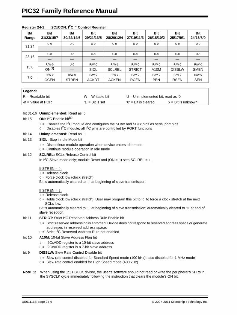
Register 24-1: I2CXCON: I2C™ Control Register Bit
RangeBit
31/23/15/7Bit
30/22/14/6Bit
29/21/13/5Bit
28/20/12/4Bit
27/19/11/3Bit
26/18/10/2Bit
25/17/9/1Bit
24/16/8/0
31:24U-0 U-0 U-0 U-0 U-0 U-0 U-0 U-0
— — — — — — — —
23:16U-0 U-0 U-0 U-0 U-0 U-0 U-0 U-0
— — — — — — — —
15:8R/W-0 U-0 R/W-0 R/W-1 R/W-0 R/W-0 R/W-0 R/W-0
ON(1) — SIDL SCLREL STRICT A10M DISSLW SMEN
7:0R/W-0 R/W-0 R/W-0 R/W-0 R/W-0 R/W-0 R/W-0 R/W-0
GCEN STREN ACKDT ACKEN RCEN PEN RSEN SEN
Legend:R = Readable bit W = Writable bit U = Unimplemented bit, read as ‘0’-n = Value at POR ‘1’ = Bit is set ‘0’ = Bit is cleared x = Bit is unknown
bit 31-16 Unimplemented: Read as ‘0’bit 15 ON: I2C Enable bit(1)
1 = Enables the I2C module and configures the SDAx and SCLx pins as serial port pins0 = Disables I2C module; all I2C pins are controlled by PORT functions
bit 14 Unimplemented: Read as ‘0’bit 13 SIDL: Stop in Idle Mode bit
1 = Discontinue module operation when device enters Idle mode0 = Continue module operation in Idle mode
bit 12 SCLREL: SCLx Release Control bitIn I2C Slave mode only; module Reset and (ON = 0) sets SCLREL = 1.
If STREN = 0:1 = Release clock0 = Force clock low (clock stretch)Bit is automatically cleared to ‘0’ at beginning of slave transmission.
If STREN = 1:1 = Release clock0 = Holds clock low (clock stretch). User may program this bit to ‘0’ to force a clock stretch at the next
SCLx low.Bit is automatically cleared to ‘0’ at beginning of slave transmission; automatically cleared to ‘0’ at end of slave reception.
bit 11 STRICT: Strict I2C Reserved Address Rule Enable bit1 = Strict reserved addressing is enforced. Device does not respond to reserved address space or generate
addresses in reserved address space.0 = Strict I2C Reserved Address Rule not enabled
bit 10 A10M: 10-bit Slave Address Flag bit1 = I2CxADD register is a 10-bit slave address0 = I2CxADD register is a 7-bit slave address
bit 9 DISSLW: Slew Rate Control Disable bit1 = Slew rate control disabled for Standard Speed mode (100 kHz); also disabled for 1 MHz mode0 = Slew rate control enabled for High Speed mode (400 kHz)
Note 1: When using the 1:1 PBCLK divisor, the user’s software should not read or write the peripheral’s SFRs in the SYSCLK cycle immediately following the instruction that clears the module’s ON bit.
DS61116E-page 24-6 © 2007-2011 Microchip Technology Inc.

Section 24. Inter-Integrated Circuit™ (I2C™)Inter-Integrated C
ircuit™ (I 2C
™)
24
bit 8 SMEN: SMBus Input Levels Disable bit1 = Enable input logic so that thresholds are compliant with the SMBus specification0 = Disable SMBus specific inputs
bit 7 GCEN: General Call Enable bit In I2C Slave mode only1 = Enable interrupt when a general call address is received in I2CSR. Module is enabled for
reception0 = General call address disabled
bit 6 STREN: SCLx Clock Stretch Enable bit In I2C Slave mode only; used in conjunction with SCLREL bit.1 = Enable clock stretching0 = Disable clock stretching
bit 5 ACKDT: Acknowledge Data bit In I2C Master mode only; applicable during master receive. Value that will be transmitted when the user initiates an Acknowledge sequence at the end of a receive.1 = A NACK is sent0 = ACK is sent
bit 4 ACKEN: Acknowledge Sequence Enable bit In I2C Master mode only; applicable during master receive1 = Initiate Acknowledge sequence on SDAx and SCLx pins, and transmit ACKDT data bit; cleared by
module0 = Acknowledge sequence idle
bit 3 RCEN: Receive Enable bit In I2C Master mode only1 = Enables Receive mode for I2C, automatically cleared by module at end of 8-bit receive data byte0 = Receive sequence not in progress
bit 2 PEN: Stop Condition Enable bit In I2C Master mode only1 = Initiate Stop condition on SDAx and SCLx pins; cleared by module0 = Stop condition idle
bit 1 RSEN: Restart Condition Enable bit In I2C Master mode only1 = Initiate Restart condition on SDAx and SCLx pins; cleared by module0 = Restart condition idle
bit 0 SEN: Start Condition Enable bit In I2C Master mode only1 = Initiate Start condition on SDAx and SCLx pins; cleared by module0 = Start condition idle
Register 24-1: I2CXCON: I2C™ Control Register (Continued)
Note 1: When using the 1:1 PBCLK divisor, the user’s software should not read or write the peripheral’s SFRs in the SYSCLK cycle immediately following the instruction that clears the module’s ON bit.
© 2007-2011 Microchip Technology Inc. DS61116E-page 24-7

PIC32 Family Reference Manual
Register 24-2: I2CXSTAT: I2C™ Status Register Bit
RangeBit
31/23/15/7Bit
30/22/14/6Bit
29/21/13/5Bit
28/20/12/4Bit
27/19/11/3Bit
26/18/10/2Bit
25/17/9/1Bit
24/16/8/0
31:24U-0 U-0 U-0 U-0 U-0 U-0 U-0 U-0
— — — — — — — —
23:16U-0 U-0 U-0 U-0 U-0 U-0 U-0 U-0
— — — — — — — —
15:8R-0 R-0 U-0 U-0 U-0 R/W-0 R-0 R-0
ACKSTAT TRSTAT — — — BCL GCSTAT ADD10
7:0R/W-0 R/W-0 R-0 R/W-0 R/W-0 R-0 R-0 R-0
IWCOL I2COV D/A P S R/W RBF TBF
Legend:R = Readable bit W = Writable bit U = Unimplemented bit, read as ‘0’-n = Value at POR ‘1’ = Bit is set ‘0’ = Bit is cleared x = Bit is unknown
bit 31-16 Unimplemented: Read as ‘0’bit 15 ACKSTAT: Acknowledge Status bit
In both I2C Master and Slave modes; applicable to both transmit and receive.1 = Acknowledge was not received0 = Acknowledge was received
bit 14 TRSTAT: Transmit Status bit In I2C Master mode only; applicable to Master Transmit mode.1 = Master transmit is in progress (8 bits + ACK)0 = Master transmit is not in progress
bit 13-11 Unimplemented: Read as ‘0’bit 10 BCL: Master Bus Collision Detect bit
Cleared when the I2C module is disabled (ON = 0).1 = A bus collision has been detected during a master operation0 = No collision has been detected
bit 9 GCSTAT: General Call Status bit Cleared after Stop detection.1 = General call address was received0 = General call address was not received
bit 8 ADD10: 10-bit Address Status bit Cleared after Stop detection.1 = 10-bit address was matched0 = 10-bit address was not matched
bit 7 IWCOL: Write Collision Detect bit1 = An attempt to write the I2CxTRN register collided because the I2C module is busy.
This bit must be cleared in software.0 = No collision
bit 6 I2COV: I2C Receive Overflow Status bit1 = A byte is received while the I2CxRCV register is still holding the previous byte.
I2COV is a “don’t care” in Transmit mode. This bit must be cleared in software.0 = No overflow
bit 5 D/A: Data/Address bit Valid only for Slave mode operation.1 = Indicates that the last byte received or transmitted was data0 = Indicates that the last byte received or transmitted was address
DS61116E-page 24-8 © 2007-2011 Microchip Technology Inc.
Section 24. Inter-Integrated Circuit™ (I2C™)Inter-Integrated C
ircuit™ (I 2C
™)
24
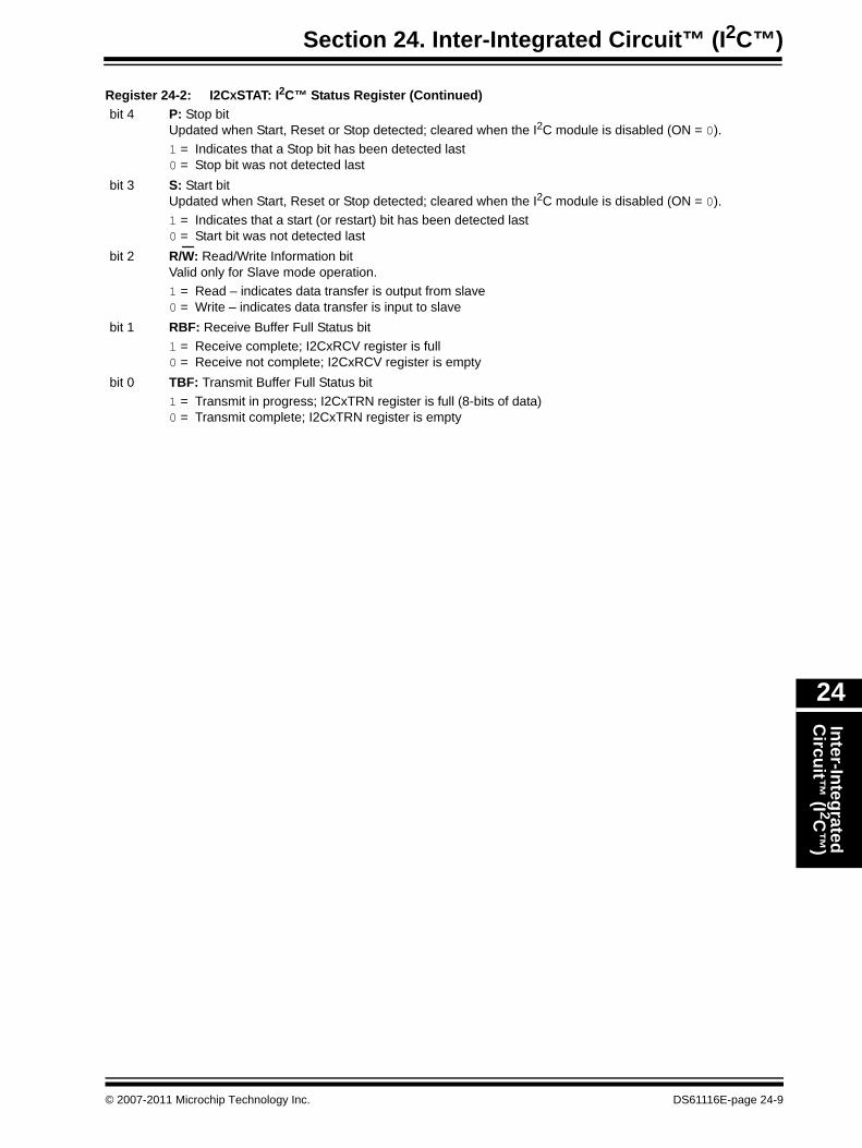
bit 4 P: Stop bit Updated when Start, Reset or Stop detected; cleared when the I2C module is disabled (ON = 0).1 = Indicates that a Stop bit has been detected last0 = Stop bit was not detected last
bit 3 S: Start bit Updated when Start, Reset or Stop detected; cleared when the I2C module is disabled (ON = 0).1 = Indicates that a start (or restart) bit has been detected last0 = Start bit was not detected last
bit 2 R/W: Read/Write Information bit Valid only for Slave mode operation.1 = Read – indicates data transfer is output from slave0 = Write – indicates data transfer is input to slave
bit 1 RBF: Receive Buffer Full Status bit1 = Receive complete; I2CxRCV register is full0 = Receive not complete; I2CxRCV register is empty
bit 0 TBF: Transmit Buffer Full Status bit1 = Transmit in progress; I2CxTRN register is full (8-bits of data)0 = Transmit complete; I2CxTRN register is empty
Register 24-2: I2CXSTAT: I2C™ Status Register (Continued)
© 2007-2011 Microchip Technology Inc. DS61116E-page 24-9
PIC32 Family Reference Manual
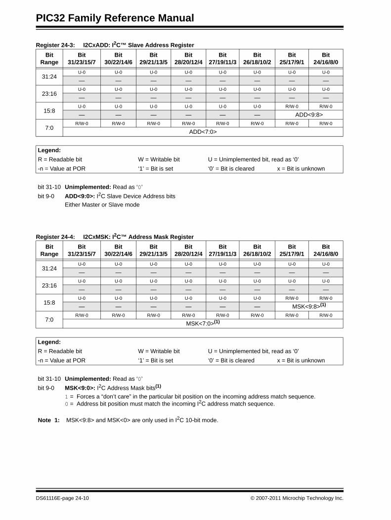
Register 24-3: I2CXADD: I2C™ Slave Address Register Bit
RangeBit
31/23/15/7Bit
30/22/14/6Bit
29/21/13/5Bit
28/20/12/4Bit
27/19/11/3Bit
26/18/10/2Bit
25/17/9/1Bit
24/16/8/0
31:24U-0 U-0 U-0 U-0 U-0 U-0 U-0 U-0
— — — — — — — —
23:16U-0 U-0 U-0 U-0 U-0 U-0 U-0 U-0
— — — — — — — —
15:8U-0 U-0 U-0 U-0 U-0 U-0 R/W-0 R/W-0
— — — — — — ADD<9:8>
7:0R/W-0 R/W-0 R/W-0 R/W-0 R/W-0 R/W-0 R/W-0 R/W-0
ADD<7:0>
Legend:R = Readable bit W = Writable bit U = Unimplemented bit, read as ‘0’-n = Value at POR ‘1’ = Bit is set ‘0’ = Bit is cleared x = Bit is unknown
bit 31-10 Unimplemented: Read as ‘0’bit 9-0 ADD<9:0>: I2C Slave Device Address bits
Either Master or Slave mode
Register 24-4: I2CXMSK: I2C™ Address Mask Register Bit
RangeBit
31/23/15/7Bit
30/22/14/6Bit
29/21/13/5Bit
28/20/12/4Bit
27/19/11/3Bit
26/18/10/2Bit
25/17/9/1Bit
24/16/8/0
31:24U-0 U-0 U-0 U-0 U-0 U-0 U-0 U-0
— — — — — — — —
23:16U-0 U-0 U-0 U-0 U-0 U-0 U-0 U-0
— — — — — — — —
15:8U-0 U-0 U-0 U-0 U-0 U-0 R/W-0 R/W-0
— — — — — — MSK<9:8>(1)
7:0R/W-0 R/W-0 R/W-0 R/W-0 R/W-0 R/W-0 R/W-0 R/W-0
MSK<7:0>(1)
Legend:R = Readable bit W = Writable bit U = Unimplemented bit, read as ‘0’-n = Value at POR ‘1’ = Bit is set ‘0’ = Bit is cleared x = Bit is unknown
bit 31-10 Unimplemented: Read as ‘0’bit 9-0 MSK<9:0>: I2C Address Mask bits(1)
1 = Forces a “don’t care” in the particular bit position on the incoming address match sequence.0 = Address bit position must match the incoming I2C address match sequence.
Note 1: MSK<9:8> and MSK<0> are only used in I2C 10-bit mode.
DS61116E-page 24-10 © 2007-2011 Microchip Technology Inc.
Section 24. Inter-Integrated Circuit™ (I2C™)Inter-Integrated C
ircuit™ (I 2C
™)
24
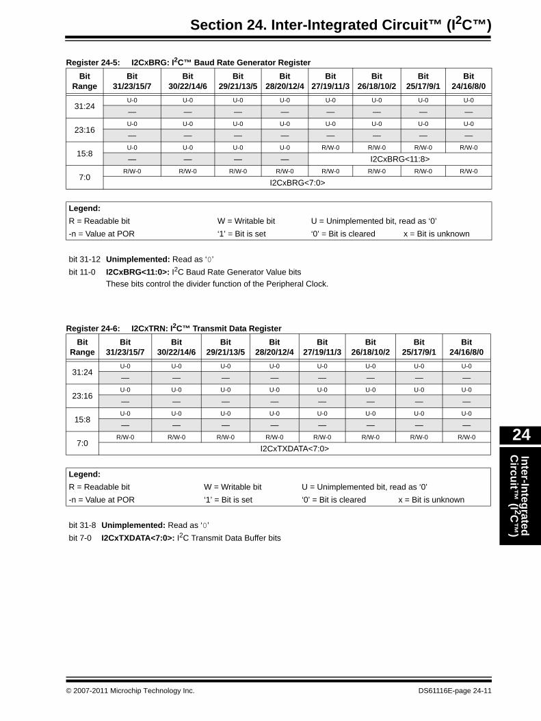
Register 24-5: I2CXBRG: I2C™ Baud Rate Generator Register Bit
RangeBit
31/23/15/7Bit
30/22/14/6Bit
29/21/13/5Bit
28/20/12/4Bit
27/19/11/3Bit
26/18/10/2Bit
25/17/9/1Bit
24/16/8/0
31:24U-0 U-0 U-0 U-0 U-0 U-0 U-0 U-0
— — — — — — — —
23:16U-0 U-0 U-0 U-0 U-0 U-0 U-0 U-0
— — — — — — — —
15:8U-0 U-0 U-0 U-0 R/W-0 R/W-0 R/W-0 R/W-0
— — — — I2CxBRG<11:8>
7:0R/W-0 R/W-0 R/W-0 R/W-0 R/W-0 R/W-0 R/W-0 R/W-0
I2CxBRG<7:0>
Legend:R = Readable bit W = Writable bit U = Unimplemented bit, read as ‘0’-n = Value at POR ‘1’ = Bit is set ‘0’ = Bit is cleared x = Bit is unknown
bit 31-12 Unimplemented: Read as ‘0’bit 11-0 I2CxBRG<11:0>: I2C Baud Rate Generator Value bits
These bits control the divider function of the Peripheral Clock.
Register 24-6: I2CXTRN: I2C™ Transmit Data Register Bit
RangeBit
31/23/15/7Bit
30/22/14/6Bit
29/21/13/5Bit
28/20/12/4Bit
27/19/11/3Bit
26/18/10/2Bit
25/17/9/1Bit
24/16/8/0
31:24U-0 U-0 U-0 U-0 U-0 U-0 U-0 U-0
— — — — — — — —
23:16U-0 U-0 U-0 U-0 U-0 U-0 U-0 U-0
— — — — — — — —
15:8U-0 U-0 U-0 U-0 U-0 U-0 U-0 U-0
— — — — — — — —
7:0R/W-0 R/W-0 R/W-0 R/W-0 R/W-0 R/W-0 R/W-0 R/W-0
I2CxTXDATA<7:0>
Legend:R = Readable bit W = Writable bit U = Unimplemented bit, read as ‘0’-n = Value at POR ‘1’ = Bit is set ‘0’ = Bit is cleared x = Bit is unknown
bit 31-8 Unimplemented: Read as ‘0’bit 7-0 I2CxTXDATA<7:0>: I2C Transmit Data Buffer bits
© 2007-2011 Microchip Technology Inc. DS61116E-page 24-11
PIC32 Family Reference Manual
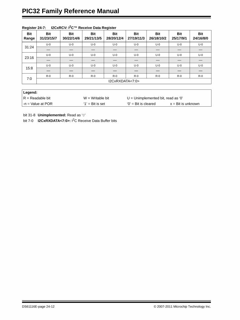
Register 24-7: I2CxRCV: I2C™ Receive Data Register Bit
RangeBit
31/23/15/7Bit
30/22/14/6Bit
29/21/13/5Bit
28/20/12/4Bit
27/19/11/3Bit
26/18/10/2Bit
25/17/9/1Bit
24/16/8/0
31:24U-0 U-0 U-0 U-0 U-0 U-0 U-0 U-0
— — — — — — — —
23:16U-0 U-0 U-0 U-0 U-0 U-0 U-0 U-0
— — — — — — — —
15:8U-0 U-0 U-0 U-0 U-0 U-0 U-0 U-0
— — — — — — — —
7:0R-0 R-0 R-0 R-0 R-0 R-0 R-0 R-0
I2CxRXDATA<7:0>
Legend:R = Readable bit W = Writable bit U = Unimplemented bit, read as ‘0’-n = Value at POR ‘1’ = Bit is set ‘0’ = Bit is cleared x = Bit is unknown
bit 31-8 Unimplemented: Read as ‘0’bit 7-0 I2CxRXDATA<7:0>: I2C Receive Data Buffer bits
DS61116E-page 24-12 © 2007-2011 Microchip Technology Inc.
Section 24. Inter-Integrated Circuit™ (I2C™)Inter-Integrated C
ircuit™ (I 2C
™)
24
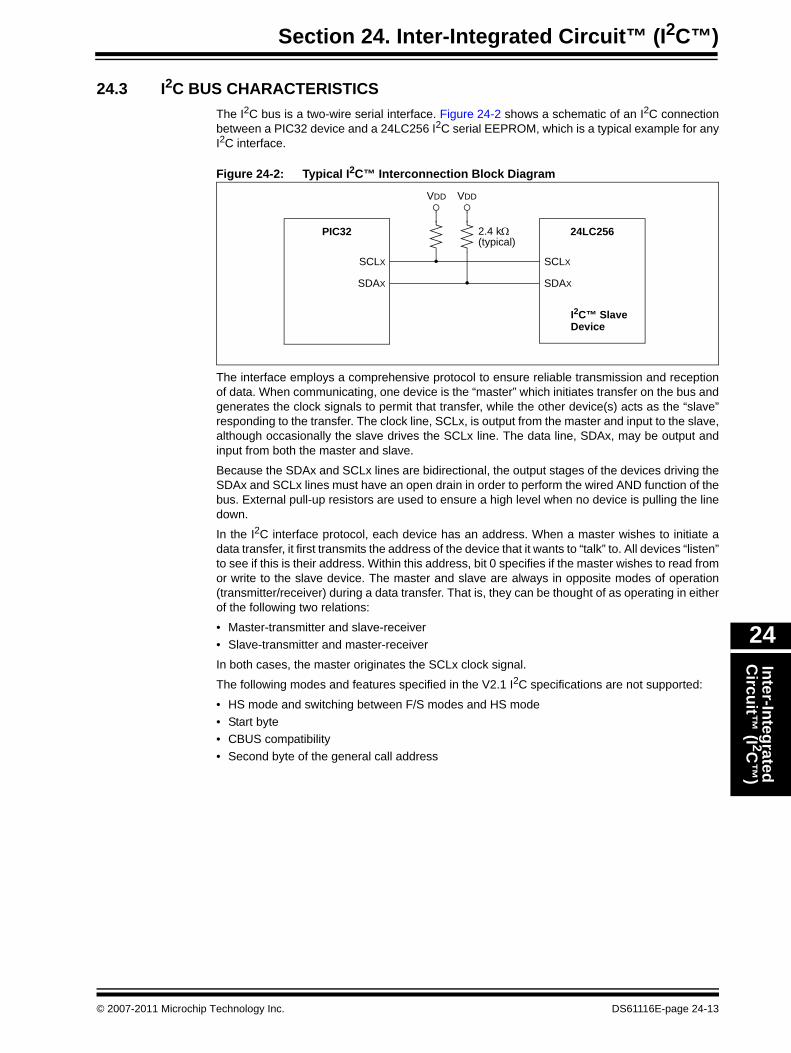
24.3 I2C BUS CHARACTERISTICSThe I2C bus is a two-wire serial interface. Figure 24-2 shows a schematic of an I2C connection between a PIC32 device and a 24LC256 I2C serial EEPROM, which is a typical example for any I2C interface.
Figure 24-2: Typical I2C™ Interconnection Block Diagram
The interface employs a comprehensive protocol to ensure reliable transmission and reception of data. When communicating, one device is the “master” which initiates transfer on the bus and generates the clock signals to permit that transfer, while the other device(s) acts as the “slave” responding to the transfer. The clock line, SCLx, is output from the master and input to the slave, although occasionally the slave drives the SCLx line. The data line, SDAx, may be output and input from both the master and slave.
Because the SDAx and SCLx lines are bidirectional, the output stages of the devices driving the SDAx and SCLx lines must have an open drain in order to perform the wired AND function of the bus. External pull-up resistors are used to ensure a high level when no device is pulling the line down.
In the I2C interface protocol, each device has an address. When a master wishes to initiate a data transfer, it first transmits the address of the device that it wants to “talk” to. All devices “listen” to see if this is their address. Within this address, bit 0 specifies if the master wishes to read from or write to the slave device. The master and slave are always in opposite modes of operation (transmitter/receiver) during a data transfer. That is, they can be thought of as operating in either of the following two relations:
• Master-transmitter and slave-receiver• Slave-transmitter and master-receiver
In both cases, the master originates the SCLx clock signal.
The following modes and features specified in the V2.1 I2C specifications are not supported:
• HS mode and switching between F/S modes and HS mode• Start byte• CBUS compatibility• Second byte of the general call address
SCLX
SDAX
PIC32
SDAX
SCLX
VDD VDD
2.4 kΩ 24LC256(typical)
I2C™ SlaveDevice
© 2007-2011 Microchip Technology Inc. DS61116E-page 24-13
PIC32 Family Reference Manual
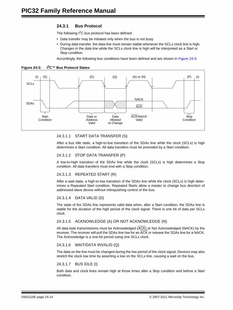
24.3.1 Bus ProtocolThe following I2C bus protocol has been defined:
• Data transfer may be initiated only when the bus is not busy• During data transfer, the data line must remain stable whenever the SCLx clock line is high.
Changes in the data line while the SCLx clock line is high will be interpreted as a Start or Stop condition.
Accordingly, the following bus conditions have been defined and are shown in Figure 24-3.
Figure 24-3: I2C™ Bus Protocol States
24.3.1.1 START DATA TRANSFER (S)
After a bus Idle state, a high-to-low transition of the SDAx line while the clock (SCLx) is high determines a Start condition. All data transfers must be preceded by a Start condition.
24.3.1.2 STOP DATA TRANSFER (P)
A low-to-high transition of the SDAx line while the clock (SCLx) is high determines a Stop condition. All data transfers must end with a Stop condition.
24.3.1.3 REPEATED START (R)
After a wait state, a high-to-low transition of the SDAx line while the clock (SCLx) is high deter-mines a Repeated Start condition. Repeated Starts allow a master to change bus direction of addressed slave device without relinquishing control of the bus.
24.3.1.4 DATA VALID (D)
The state of the SDAx line represents valid data when, after a Start condition, the SDAx line is stable for the duration of the high period of the clock signal. There is one bit of data per SCLx clock.
24.3.1.5 ACKNOWLEDGE (A) OR NOT ACKNOWLEDGE (N)
All data byte transmissions must be Acknowledged (ACK) or Not Acknowledged (NACK) by the receiver. The receiver will pull the SDAx line low for an ACK or release the SDAx line for a NACK. The Acknowledge is a one-bit period using one SCLx clock.
24.3.1.6 WAIT/DATA INVALID (Q)
The data on the line must be changed during the low period of the clock signal. Devices may also stretch the clock low time by asserting a low on the SCLx line, causing a wait on the bus.
24.3.1.7 BUS IDLE (I)
Both data and clock lines remain high at those times after a Stop condition and before a Start condition.
AddressValid
DataAllowed
to Change
StopCondition
StartCondition
SCLx
SDAx
(I) (S) (D) (A) or (N) (P) (I)
Data or
(Q)
ACK/NACKValid
NACK
ACK
DS61116E-page 24-14 © 2007-2011 Microchip Technology Inc.
Section 24. Inter-Integrated Circuit™ (I2C™)Inter-Integrated C
ircuit™ (I 2C
™)
24
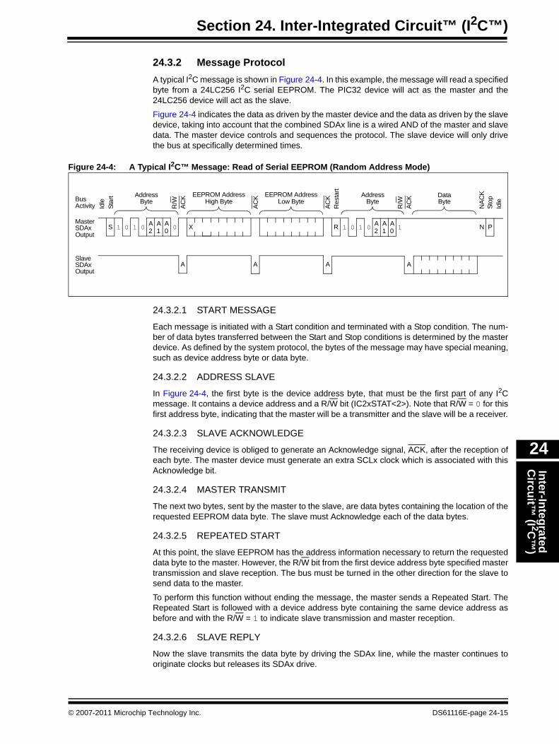
24.3.2 Message ProtocolA typical I2C message is shown in Figure 24-4. In this example, the message will read a specified byte from a 24LC256 I2C serial EEPROM. The PIC32 device will act as the master and the 24LC256 device will act as the slave.
Figure 24-4 indicates the data as driven by the master device and the data as driven by the slave device, taking into account that the combined SDAx line is a wired AND of the master and slave data. The master device controls and sequences the protocol. The slave device will only drive the bus at specifically determined times.
Figure 24-4: A Typical I2C™ Message: Read of Serial EEPROM (Random Address Mode)
24.3.2.1 START MESSAGE
Each message is initiated with a Start condition and terminated with a Stop condition. The num-ber of data bytes transferred between the Start and Stop conditions is determined by the master device. As defined by the system protocol, the bytes of the message may have special meaning, such as device address byte or data byte.
24.3.2.2 ADDRESS SLAVE
In Figure 24-4, the first byte is the device address byte, that must be the first part of any I2C message. It contains a device address and a R/W bit (IC2xSTAT<2>). Note that R/W = 0 for this first address byte, indicating that the master will be a transmitter and the slave will be a receiver.
24.3.2.3 SLAVE ACKNOWLEDGE
The receiving device is obliged to generate an Acknowledge signal, ACK, after the reception of each byte. The master device must generate an extra SCLx clock which is associated with this Acknowledge bit.
24.3.2.4 MASTER TRANSMIT
The next two bytes, sent by the master to the slave, are data bytes containing the location of the requested EEPROM data byte. The slave must Acknowledge each of the data bytes.
24.3.2.5 REPEATED START
At this point, the slave EEPROM has the address information necessary to return the requested data byte to the master. However, the R/W bit from the first device address byte specified master transmission and slave reception. The bus must be turned in the other direction for the slave to send data to the master.
To perform this function without ending the message, the master sends a Repeated Start. The Repeated Start is followed with a device address byte containing the same device address as before and with the R/W = 1 to indicate slave transmission and master reception.
24.3.2.6 SLAVE REPLY
Now the slave transmits the data byte by driving the SDAx line, while the master continues to originate clocks but releases its SDAx drive.
X
Bus
MasterSDAx
Star
t AddressByte
EEPROM AddressHigh Byte
EEPROM AddressLow Byte
AddressByte
DataByte
S 1 0 1 0 A A A 02 1 0 R 1 0 1 0 A A A 12 1 0 P
SlaveSDAx
Activity
N
AAAA
Output
Output
Idle
R/W
ACK
ACK
ACK
Res
tart
R/W
ACK
NAC
KSt
opId
le
© 2007-2011 Microchip Technology Inc. DS61116E-page 24-15
PIC32 Family Reference Manual
24.3.2.7 MASTER ACKNOWLEDGE
During reads, a master must terminate data requests to the slave by Not Acknowledging (gener-ating a “NACK”) on the last byte of the message. Data is “Acked” for each byte, except for the last byte.
24.3.2.8 STOP MESSAGE
The master sends a Stop to terminate the message and return the bus to an Idle state.
DS61116E-page 24-16 © 2007-2011 Microchip Technology Inc.
Section 24. Inter-Integrated Circuit™ (I2C™)Inter-Integrated C
ircuit™ (I 2C
™)
24
24.4 ENABLING I2C OPERATIONThe I2C module fully implements all master and slave functions and is enabled by setting the ON bit (I2CxCON<15>). When the module is enabled, the master and slave functions are active simultaneously and will respond according to the software or bus events.
When initially enabled, the module will release the SDAx and SCLx pins, putting the bus into the Idle state. The master functions will remain in the Idle state unless software sets a control bit to initiate a master event. The slave functions will begin to monitor the bus. If the slave logic detects a Start event and a valid address on the bus, the slave logic will begin a slave transaction.
24.4.1 Enabling I2C I/OTwo pins are used for bus operation. These are the SCLx pin, which is the clock, and the SDAx pin, which is the data. When the module is enabled, assuming no other module with higher priority has control, the module will assume control of the SDAx and SCLx pins. The module soft-ware need not be concerned with the state of the port I/O of the pins, the module overrides, the port state, and direction. At initialization, the pins are tri-state (released).
24.4.2 I2C InterruptsThe I2C module generates three interrupt signals:
• Slave interrupt• Master interrupt• Bus collision interrupt
The slave interrupt, master interrupt and bus collision interrupt signals are pulsed high for at least one Peripheral Bus Clock (PBCLK) on the falling edge of the ninth clock pulse of the SCLx clock. These interrupts will set the corresponding interrupt flag bit and will interrupt the CPU if the corresponding interrupt enable bit is set and the corresponding interrupt priority is high enough.
Master mode operations that generate a master interrupt are:
• Start Condition – 1 BRG time after falling edge of SDAx• Repeated Start Sequence – 1 BRG time after falling edge of SDAx• Stop Condition – 1 BRG time after the rising edge of SDAx• Data transfer byte received – Eighth falling edge of SCLx (after receiving eight bits of data
from slave)• During a Send ACK sequence – Ninth falling edge of SCLx (after sending ACK or NACK to
slave)• Data transfer byte transmitted – Ninth falling edge of SCLx (regardless of receiving ACK
from slave)• During a slave-detected Stop – When slave sets the P bit (I2CxSTAT<4>)
Slave mode operations that generate a slave interrupt are:
• Detection of a valid device address (including general call) – Ninth falling edge of SCLx (after sending ACK to master. Address must match unless the STRICT bit = 1 (I2CxCON<11>) or the GCEN bit = 1 (I2CxCON<7>)
• Reception of data – Ninth falling edge of SCLx (after sending the ACK to master)• Request to transmit data – Ninth falling edge of SCLx (regardless of receiving an ACK from
the master)
Bus Collision events that generate an interrupt are:
• During a Start sequence – SDAx sampled before Start condition• During a Start sequence – SCLx = 0 before SDAx = 0• During a Start sequence – SDAx = 0 before BRG time out• During a Repeated Start sequence – If SDAx is sampled 0 when SCLx goes high• During a Repeated Start sequence – If SCLx goes low before SDAx goes low• During a Stop sequence – If SDAx is sampled low after allowing it to float• During a Stop sequence – If SCLx goes low before SDAx goes high
© 2007-2011 Microchip Technology Inc. DS61116E-page 24-17
PIC32 Family Reference Manual
24.4.3 I2C Transmit and Receive RegistersI2CxTRN is the register to which transmit data is written. This register is used when the module operates as a master transmitting data to the slave, or as a slave sending reply data to the mas-ter. As the message progresses, the I2CxTRN register shifts out the individual bits. As a result, the I2CxTRN register may not be written to unless the bus is Idle.
Data being received by either the master or the slave is shifted into a non-accessible shift regis-ter, I2CxRSR. When a complete byte is received, the byte transfers to the I2CxRCV register. In receive operations, the I2CxRSR and I2CxRCV registers create a double-buffered receiver. This allows reception of the next byte to begin before the current byte of received data is read.
If the module receives another complete byte before the software reads the previous byte from the I2CxRCV register, a receiver overflow occurs and sets the I2COV bit (I2CxSTAT<6>). The byte in the I2CxRSR register is lost.
The I2CxADD register holds the slave device address. In 10-bit Addressing mode, all bits are rel-evant. In 7-bit Addressing mode, only the I2CxADD<6:0> bits are relevant. The A10M bit (I2CxCON<10>) specifies the expected mode of the slave address. By using the I2CxMSK register with the I2CxADD register in either Slave Addressing mode, one or more bit positions can be removed from exact address matching, allowing the module in Slave mode to respond to multiple addresses.
24.4.4 I2C Baud Rate GeneratorThe Baud Rate Generator (BRG) used for I2C Master mode operation is used to set the SCLx clock frequency for 100 kHz, 400 kHz, and 1 MHz. The BRG reload value is contained in the I2CxBRG register. The BRG will automatically begin counting on a write to the I2CxTRN register. Once the given operation is complete (i.e., transmission of the last data bit is followed by an ACK) the internal clock will automatically stop counting and the SCLx pin will remain in its last state.
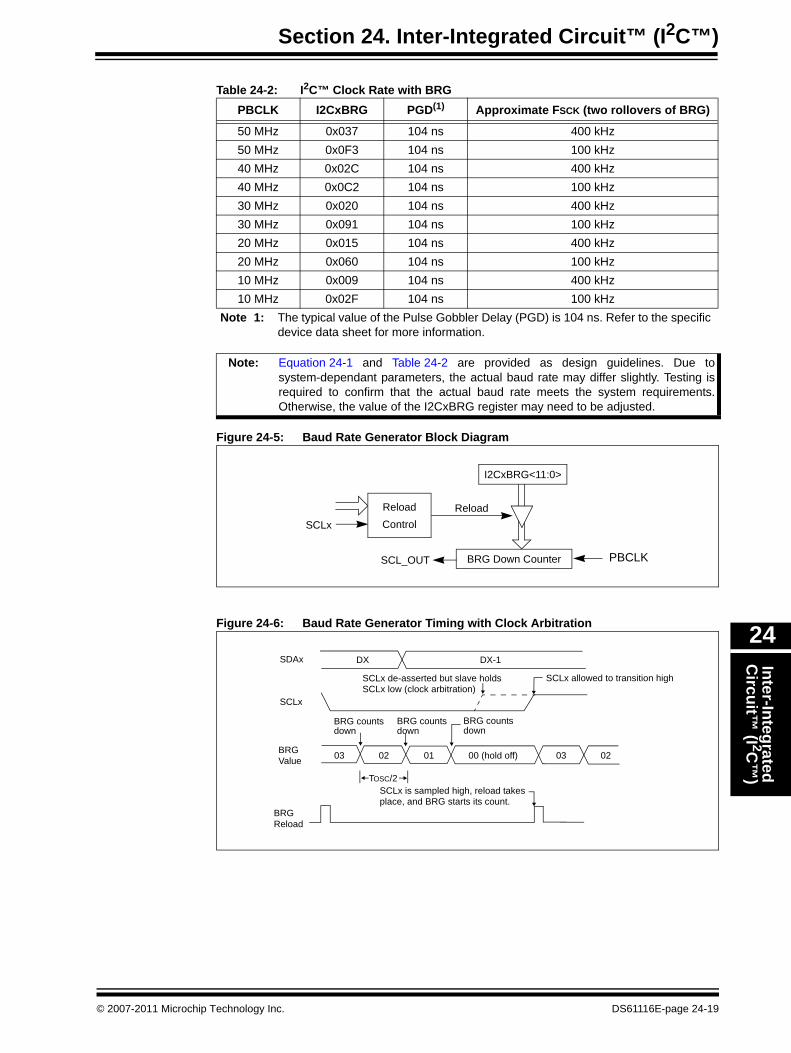
24.4.5 Baud Rate Generator in I2C Master ModeIn I2C Master mode, the reload value for the BRG is located in the I2CxBRG register. When the BRG is loaded with this value, the BRG counts down to zero and stops until another reload has taken place. In I2C Master mode, the BRG is not reloaded automatically. If clock arbitration is taking place, for instance, the BRG will be reloaded when the SCLx pin is sampled high (see Figure 24-6). Table 24-2 shows device frequency versus the I2CxBRG setting for standard baud rates.
To compute the BRG reload value, use the formula in Equation 24-1:
Equation 24-1: Baud Rate Generator Reload Value Calculation
Note: I2CxBRG values of 0x0 and 0x1 are expressly prohibited. Do not program the I2CxBRG with a value of 0x0 or 0x1, as indeterminate results may occur.
I2CxBRG 12 FSCK⋅( )
------------------------- TPGD–⎝ ⎠⎛ ⎞ PBCLK⋅ 2–=
DS61116E-page 24-18 © 2007-2011 Microchip Technology Inc.
Section 24. Inter-Integrated Circuit™ (I2C™)Inter-Integrated C
ircuit™ (I 2C
™)
24
Figure 24-5: Baud Rate Generator Block Diagram
Figure 24-6: Baud Rate Generator Timing with Clock Arbitration
Table 24-2: I2C™ Clock Rate with BRGPBCLK I2CxBRG PGD(1) Approximate FSCK (two rollovers of BRG)
50 MHz 0x037 104 ns 400 kHz50 MHz 0x0F3 104 ns 100 kHz40 MHz 0x02C 104 ns 400 kHz40 MHz 0x0C2 104 ns 100 kHz30 MHz 0x020 104 ns 400 kHz30 MHz 0x091 104 ns 100 kHz20 MHz 0x015 104 ns 400 kHz20 MHz 0x060 104 ns 100 kHz10 MHz 0x009 104 ns 400 kHz10 MHz 0x02F 104 ns 100 kHz
Note 1: The typical value of the Pulse Gobbler Delay (PGD) is 104 ns. Refer to the specific device data sheet for more information.
Note: Equation 24-1 and Table 24-2 are provided as design guidelines. Due to system-dependant parameters, the actual baud rate may differ slightly. Testing is required to confirm that the actual baud rate meets the system requirements. Otherwise, the value of the I2CxBRG register may need to be adjusted.
BRG Down CounterSCL_OUT
I2CxBRG<11:0>
SCLx
ReloadControl
Reload
PBCLK
SDAx
SCLx
SCLx de-asserted but slave holds
DX-1DX
BRG
SCLx is sampled high, reload takesplace, and BRG starts its count.
03 02 01 00 (hold off) 03 02
Reload
BRGValue
SCLx low (clock arbitration)SCLx allowed to transition high
BRG countsdown
BRG countsdown
BRG countsdown
TOSC/2
© 2007-2011 Microchip Technology Inc. DS61116E-page 24-19
PIC32 Family Reference Manual
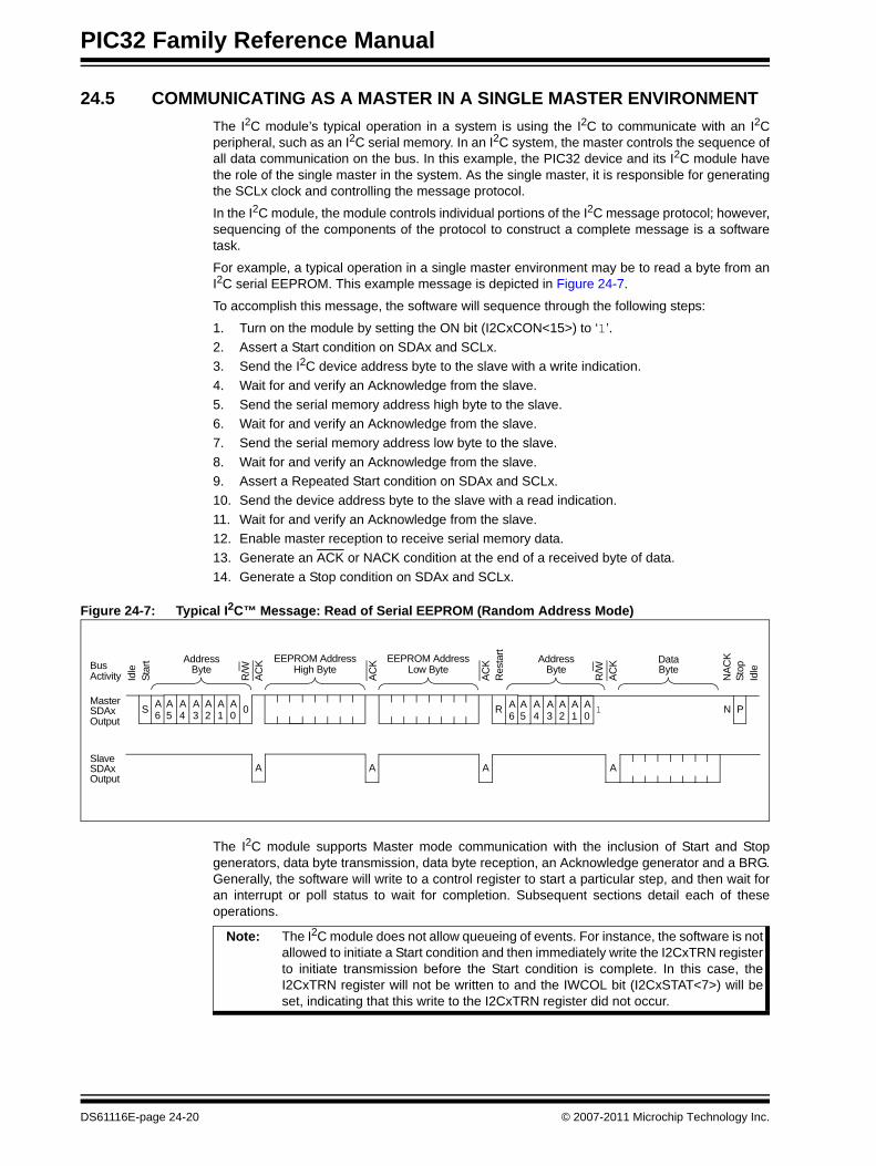
24.5 COMMUNICATING AS A MASTER IN A SINGLE MASTER ENVIRONMENTThe I2C module’s typical operation in a system is using the I2C to communicate with an I2C peripheral, such as an I2C serial memory. In an I2C system, the master controls the sequence of all data communication on the bus. In this example, the PIC32 device and its I2C module have the role of the single master in the system. As the single master, it is responsible for generating the SCLx clock and controlling the message protocol.
In the I2C module, the module controls individual portions of the I2C message protocol; however, sequencing of the components of the protocol to construct a complete message is a software task.
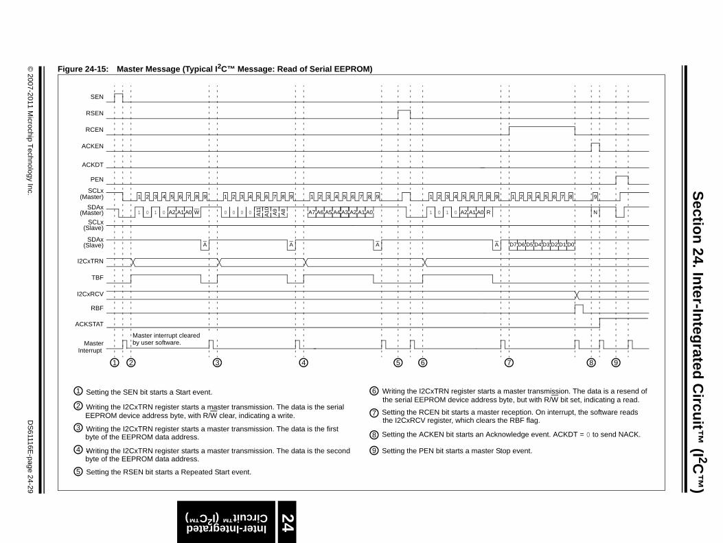
For example, a typical operation in a single master environment may be to read a byte from an I2C serial EEPROM. This example message is depicted in Figure 24-7.
To accomplish this message, the software will sequence through the following steps:
1. Turn on the module by setting the ON bit (I2CxCON<15>) to ‘1’. 2. Assert a Start condition on SDAx and SCLx.3. Send the I2C device address byte to the slave with a write indication.4. Wait for and verify an Acknowledge from the slave.5. Send the serial memory address high byte to the slave.6. Wait for and verify an Acknowledge from the slave.7. Send the serial memory address low byte to the slave.8. Wait for and verify an Acknowledge from the slave.9. Assert a Repeated Start condition on SDAx and SCLx.10. Send the device address byte to the slave with a read indication.11. Wait for and verify an Acknowledge from the slave.12. Enable master reception to receive serial memory data.13. Generate an ACK or NACK condition at the end of a received byte of data.14. Generate a Stop condition on SDAx and SCLx.
Figure 24-7: Typical I2C™ Message: Read of Serial EEPROM (Random Address Mode)
The I2C module supports Master mode communication with the inclusion of Start and Stop generators, data byte transmission, data byte reception, an Acknowledge generator and a BRG. Generally, the software will write to a control register to start a particular step, and then wait for an interrupt or poll status to wait for completion. Subsequent sections detail each of these operations.
Bus
MasterSDAx
Star
t AddressByte
EEPROM AddressHigh Byte
EEPROM AddressLow Byte
AddressByte
DataByte
S A A A 02 1 0 R 1 P
SlaveSDAx
Activity
N
AAAA
Output
Output
Idle
R/W
ACK
ACK
ACK
Res
tart
R/W
ACK
NAC
KSt
opId
le
A3
A4
A5
A6
A A A2 1 0
A3
A4
A5
A6
Note: The I2C module does not allow queueing of events. For instance, the software is not allowed to initiate a Start condition and then immediately write the I2CxTRN register to initiate transmission before the Start condition is complete. In this case, the I2CxTRN register will not be written to and the IWCOL bit (I2CxSTAT<7>) will be set, indicating that this write to the I2CxTRN register did not occur.
DS61116E-page 24-20 © 2007-2011 Microchip Technology Inc.
Section 24. Inter-Integrated Circuit™ (I2C™)Inter-Integrated C
ircuit™ (I 2C
™)
24
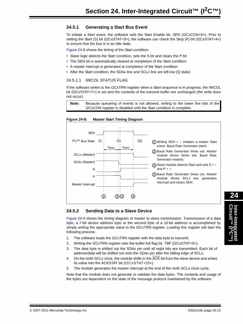
24.5.1 Generating a Start Bus EventTo initiate a Start event, the software sets the Start Enable bit, SEN (I2CxCON<0>). Prior to setting the Start (S) bit (I2CxSTAT<3>), the software can check the Stop (P) bit (I2CxSTAT<4>) to ensure that the bus is in an Idle state.
Figure 24-8 shows the timing of the Start condition.
• Slave logic detects the Start condition, sets the S bit and clears the P bit• The SEN bit is automatically cleared at completion of the Start condition• A master interrupt is generated at completion of the Start condition• After the Start condition, the SDAx line and SCLx line are left low (Q state)
24.5.1.1 IWCOL STATUS FLAG
If the software writes to the I2CxTRN register when a Start sequence is in progress, the IWCOL bit (I2CxSTAT<7>) is set and the contents of the transmit buffer are unchanged (the write doesnot occur).
Figure 24-8: Master Start Timing Diagram
24.5.2 Sending Data to a Slave DeviceFigure 24-9 shows the timing diagram of master to slave transmission. Transmission of a data byte, a 7-bit device address byte or the second byte of a 10-bit address is accomplished by simply writing the appropriate value to the I2CxTRN register. Loading this register will start the following process:
1. The software loads the I2CxTRN register with the data byte to transmit.2. Writing the I2CxTRN register sets the buffer full flag bit, TBF (I2CxSTAT<0>).3. The data byte is shifted out the SDAx pin until all eight bits are transmitted. Each bit of
address/data will be shifted out onto the SDAx pin after the falling edge of SCLx.4. On the ninth SCLx clock, the module shifts in the ACK bit from the slave device and writes
its value into the ACKSTAT bit (I2CxSTAT<15>).5. The module generates the master interrupt at the end of the ninth SCLx clock cycle.
Note that the module does not generate or validate the data bytes. The contents and usage of the bytes are dependent on the state of the message protocol maintained by the software.
Note: Because queueing of events is not allowed, writing to the lower five bits of the I2CxCON register is disabled until the Start condition is complete.
SCLx (Master)
SDAx (Master)
S
SEN
Master Interrupt
TBRG
1 2 3 4
1
TBRG2
3
4
I2C™ Bus State (I) (Q)
P
(S) Writing SEN = 1 initiates a master Start event. Baud Rate Generator starts.Baud Rate Generator times out. Master module drives SDAx low. Baud Rate Generator restarts.Slave module detects Start and sets S = 1and P = 0.Baud Rate Generator times out. Master module drives SCLx low, generates interrupt and clears SEN.
© 2007-2011 Microchip Technology Inc. DS61116E-page 24-21
PIC32 Family Reference Manual
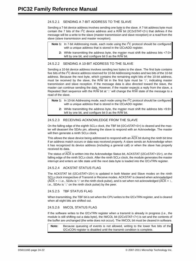
24.5.2.1 SENDING A 7-BIT ADDRESS TO THE SLAVE
Sending a 7-bit device address involves sending one byte to the slave. A 7-bit address byte must contain the 7 bits of the I2C device address and a R/W bit (IC2xSTAT<2>) that defines if the message will be a write to the slave (master transmission and slave reception) or a read from the slave (slave transmission and master reception).
24.5.2.2 SENDING A 10-BIT ADDRESS TO THE SLAVE
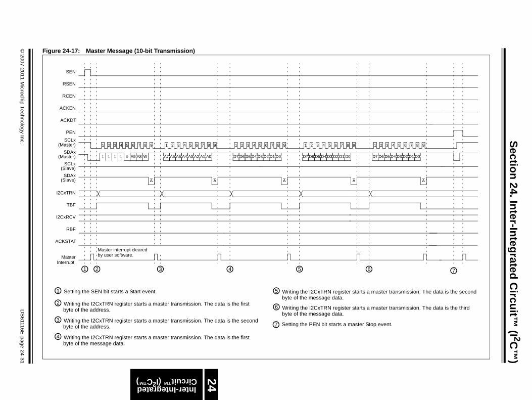
Sending a 10-bit device address involves sending two bytes to the slave. The first byte contains five bits of the I2C device address reserved for 10-bit Addressing modes and two bits of the 10-bit address. Because the next byte, which contains the remaining eight bits of the 10-bit address, must be received by the slave, the R/W bit in the first byte must be ‘0’, indicating master transmission and slave reception. If the message data is also directed toward the slave, the master can continue sending the data. However, if the master expects a reply from the slave, a Repeated Start sequence with the R/W bit at ‘1’ will change the R/W state of the message to a read of the slave.
24.5.2.3 RECEIVING ACKNOWLEDGE FROM THE SLAVE
On the falling edge of the eighth SCLx clock, the TBF bit (I2CxSTAT<0>) is cleared and the mas-ter will deassert the SDAx pin, allowing the slave to respond with an Acknowledge. The master will then generate a ninth SCLx clock.
This allows the slave device being addressed to respond with an ACK bit during the ninth bit time if an address match occurs or data was received properly. A slave sends an Acknowledge when it has recognized its device address (including a general call) or when the slave has properly received its data.
The status of ACK is written into the Acknowledge Status bit, ACKSTAT (I2CxSTAT<15>), on the falling edge of the ninth SCLx clock. After the ninth SCLx clock, the module generates the master interrupt and enters an Idle state until the next data byte is loaded into the I2CxTRN register.
24.5.2.4 ACKSTAT STATUS FLAG
The ACKSTAT bit (I2CxSTAT<15>) is updated in both Master and Slave modes on the ninth SCLx clock irrespective of Transmit or Receive modes. ACKSTAT is cleared when acknowledged (ACK = 0 i.e., SDAx is ‘0’ on the ninth clock pulse), and is set when not acknowledged (ACK = 1, i.e., SDAx is ‘1’ on the ninth clock pulse) by the peer.
24.5.2.5 TBF STATUS FLAG
When transmitting, the TBF bit is set when the CPU writes to the I2CxTRN register, and is cleared when all eight bits are shifted out.
24.5.2.6 IWCOL STATUS FLAG
If the software writes to the I2CxTRN register when a transmit is already in progress (i.e., the module is still shifting out a data byte), the IWCOL bit (I2CxSTAT<7>) is set and the contents of the buffer are unchanged (the write does not occur). The IWCOL bit must be cleared in software.
Note 1: In 7-bit Addressing mode, each node using the I2C protocol should be configured with a unique address that is stored in the I2CxADD register.
2: While transmitting the address byte, the master must shift the address bits <7:0> left by one bit, and configure bit 0 as the R/W bit.
Note 1: In 10-bit Addressing mode, each node using the I2C protocol should be configured with a unique address that is stored in the I2CxADD register.
2: While transmitting the address byte, the master must shift the address bits <9:8> left by one bit, and configure bit 0 as the R/W bit.
Note: Because queueing of events is not allowed, writing to the lower five bits of the I2CxCON register is disabled until the transmit condition is complete.
DS61116E-page 24-22 © 2007-2011 Microchip Technology Inc.
Section 24. Inter-Integrated Circuit™ (I2C™)Inter-Integrated C
ircuit™ (I 2C
™)
24
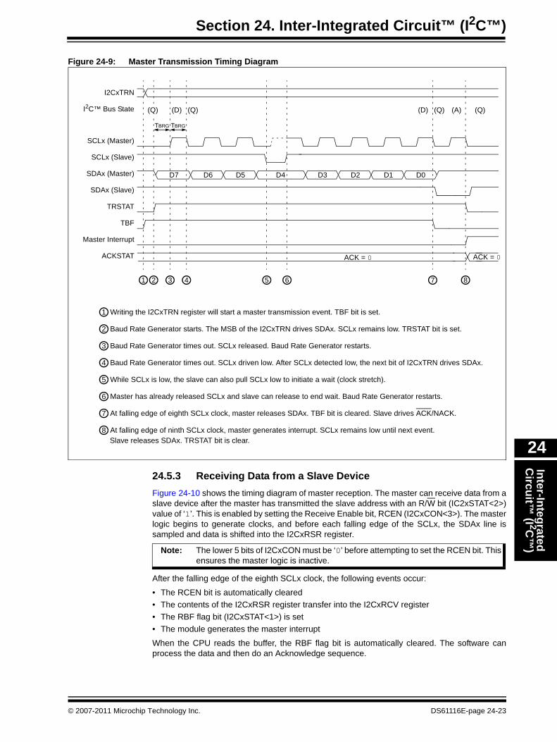
Figure 24-9: Master Transmission Timing Diagram
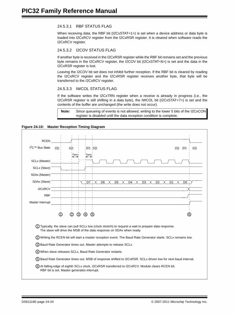
24.5.3 Receiving Data from a Slave DeviceFigure 24-10 shows the timing diagram of master reception. The master can receive data from a slave device after the master has transmitted the slave address with an R/W bit (IC2xSTAT<2>) value of ‘1’. This is enabled by setting the Receive Enable bit, RCEN (I2CxCON<3>). The master logic begins to generate clocks, and before each falling edge of the SCLx, the SDAx line is sampled and data is shifted into the I2CxRSR register.
After the falling edge of the eighth SCLx clock, the following events occur:
• The RCEN bit is automatically cleared• The contents of the I2CxRSR register transfer into the I2CxRCV register• The RBF flag bit (I2CxSTAT<1>) is set• The module generates the master interrupt
When the CPU reads the buffer, the RBF flag bit is automatically cleared. The software can process the data and then do an Acknowledge sequence.
D7 D6 D5 D4 D3 D2 D1 D0
SCLx (Master)
SCLx (Slave)
SDAx (Master)
SDAx (Slave)
TBF
I2CxTRN
Master Interrupt
TBRG TBRG
5 6 7 81 2 3 4
Writing the I2CxTRN register will start a master transmission event. TBF bit is set.1
Baud Rate Generator starts. The MSB of the I2CxTRN drives SDAx. SCLx remains low. TRSTAT bit is set.2
Baud Rate Generator times out. SCLx released. Baud Rate Generator restarts.3
Baud Rate Generator times out. SCLx driven low. After SCLx detected low, the next bit of I2CxTRN drives SDAx.4
While SCLx is low, the slave can also pull SCLx low to initiate a wait (clock stretch).5
Master has already released SCLx and slave can release to end wait. Baud Rate Generator restarts.6
At falling edge of eighth SCLx clock, master releases SDAx. TBF bit is cleared. Slave drives ACK/NACK.7
At falling edge of ninth SCLx clock, master generates interrupt. SCLx remains low until next event. 8Slave releases SDAx. TRSTAT bit is clear.
I2C™ Bus State (Q) (D) (Q) (A) (Q)(D) (Q)
TRSTAT
ACKSTAT ACK = 0 ACK = 0
Note: The lower 5 bits of I2CxCON must be ‘0’ before attempting to set the RCEN bit. This ensures the master logic is inactive.
© 2007-2011 Microchip Technology Inc. DS61116E-page 24-23
PIC32 Family Reference Manual
24.5.3.1 RBF STATUS FLAG
When receiving data, the RBF bit (I2CxSTAT<1>) is set when a device address or data byte is loaded into I2CxRCV register from the I2CxRSR register. It is cleared when software reads the I2CxRCV register.
24.5.3.2 I2COV STATUS FLAG
If another byte is received in the I2CxRSR register while the RBF bit remains set and the previous byte remains in the I2CxRCV register, the I2COV bit (I2CxSTAT<6>) is set and the data in the I2CxRSR register is lost.
Leaving the I2COV bit set does not inhibit further reception. If the RBF bit is cleared by reading the I2CxRCV register and the I2CxRSR register receives another byte, that byte will be transferred to the I2CxRCV register.
24.5.3.3 IWCOL STATUS FLAG
If the software writes the I2CxTRN register when a receive is already in progress (i.e., the I2CxRSR register is still shifting in a data byte), the IWCOL bit (I2CxSTAT<7>) is set and the contents of the buffer are unchanged (the write does not occur).
Figure 24-10: Master Reception Timing Diagram
Note: Since queueing of events is not allowed, writing to the lower 5 bits of the I2CxCON register is disabled until the data reception condition is complete.
D7 D6 D5 D4 D3 D2 D1 D0
SCLx (Master)
SCLx (Slave)
SDAx (Slave)
SDAx (Master)
RBF
I2C™ Bus State
Master Interrupt
TBRG
5 62 3 4
Writing the RCEN bit will start a master reception event. The Baud Rate Generator starts. SCLx remains low.2
Baud Rate Generator times out. Master attempts to release SCLx. 3
When slave releases SCLx, Baud Rate Generator restarts.4
Baud Rate Generator times out. MSB of response shifted to I2CxRSR. SCLx driven low for next baud interval. 5
At falling edge of eighth SCLx clock, I2CxRSR transferred to I2CxRCV. Module clears RCEN bit. 6
TBRG
RCEN
(D) (Q) (Q)(D)(Q)
I2CxRCV
RBF bit is set. Master generates interrupt.
(Q)
1
Typically, the slave can pull SCLx low (clock stretch) to request a wait to prepare data response. 1The slave will drive the MSB of the data response on SDAx when ready.
(Q)
DS61116E-page 24-24 © 2007-2011 Microchip Technology Inc.
Section 24. Inter-Integrated Circuit™ (I2C™)Inter-Integrated C
ircuit™ (I 2C
™)
24
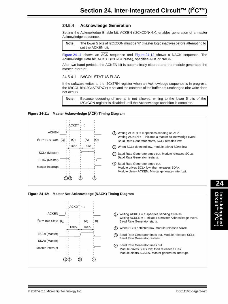
24.5.4 Acknowledge GenerationSetting the Acknowledge Enable bit, ACKEN (I2CxCON<4>), enables generation of a master Acknowledge sequence.
Figure 24-11 shows an ACK sequence and Figure 24-12 shows a NACK sequence. The Acknowledge Data bit, ACKDT (I2CxCON<5>), specifies ACK or NACK.
After two baud periods, the ACKEN bit is automatically cleared and the module generates the master interrupt.
24.5.4.1 IWCOL STATUS FLAG
If the software writes to the I2CxTRN register when an Acknowledge sequence is in progress, the IWCOL bit (I2CxSTAT<7>) is set and the contents of the buffer are unchanged (the write doesnot occur).
Figure 24-11: Master Acknowledge (ACK) Timing Diagram
Figure 24-12: Master Not Acknowledge (NACK) Timing Diagram
Note: The lower 5 bits of I2CxCON must be ‘0’ (master logic inactive) before attempting to set the ACKEN bit.
Note: Because queueing of events is not allowed, writing to the lower 5 bits of the I2CxCON register is disabled until the Acknowledge condition is complete.
SCLx (Master)
SDAx (Master)
ACKEN
Master Interrupt
TBRG
1 2 3
Writing ACKEN = 1 initiates a master Acknowledge event. 1
TBRG
Writing ACKDT = 0 specifies sending an ACK.
When SCLx detected low, module drives SDAx low. 2
Baud Rate Generator times out. Module releases SCLx.3
Baud Rate Generator times out. 4
I2C™ Bus State (A) (Q)(Q)
4
Baud Rate Generator restarts.
Baud Rate Generator starts. SCLx remains low.
Module drives SCLx low, then releases SDAx.Module clears ACKEN. Master generates interrupt.
(Q)
ACKDT = 0
SCLx (Master)
SDAx (Master)
ACKEN
Master Interrupt
TBRG
1 2 3
Writing ACKEN = 1 initiates a master Acknowledge event. 1
TBRG
Writing ACKDT = 1 specifies sending a NACK.
When SCLx detected low, module releases SDAx.2
Baud Rate Generator times out. Module releases SCLx.3
Baud Rate Generator times out. 4
I2C™ Bus State (A) (I)(Q)
4
Baud Rate Generator restarts.
Baud Rate Generator starts.
Module drives SCLx low, then releases SDAx.Module clears ACKEN. Master generates interrupt.
ACKDT = 1
© 2007-2011 Microchip Technology Inc. DS61116E-page 24-25
PIC32 Family Reference Manual
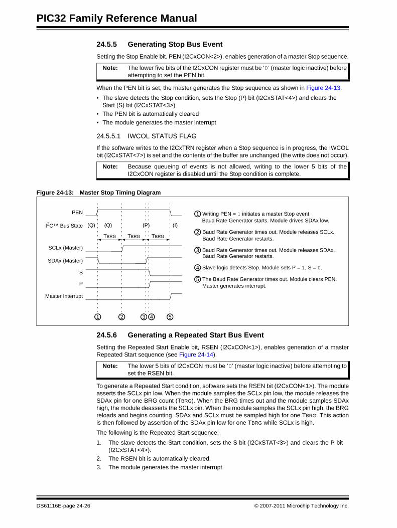
24.5.5 Generating Stop Bus EventSetting the Stop Enable bit, PEN (I2CxCON<2>), enables generation of a master Stop sequence.
When the PEN bit is set, the master generates the Stop sequence as shown in Figure 24-13.
• The slave detects the Stop condition, sets the Stop (P) bit (I2CxSTAT<4>) and clears the Start (S) bit (I2CxSTAT<3>)
• The PEN bit is automatically cleared• The module generates the master interrupt
24.5.5.1 IWCOL STATUS FLAG
If the software writes to the I2CxTRN register when a Stop sequence is in progress, the IWCOL bit (I2CxSTAT<7>) is set and the contents of the buffer are unchanged (the write does not occur).
Figure 24-13: Master Stop Timing Diagram
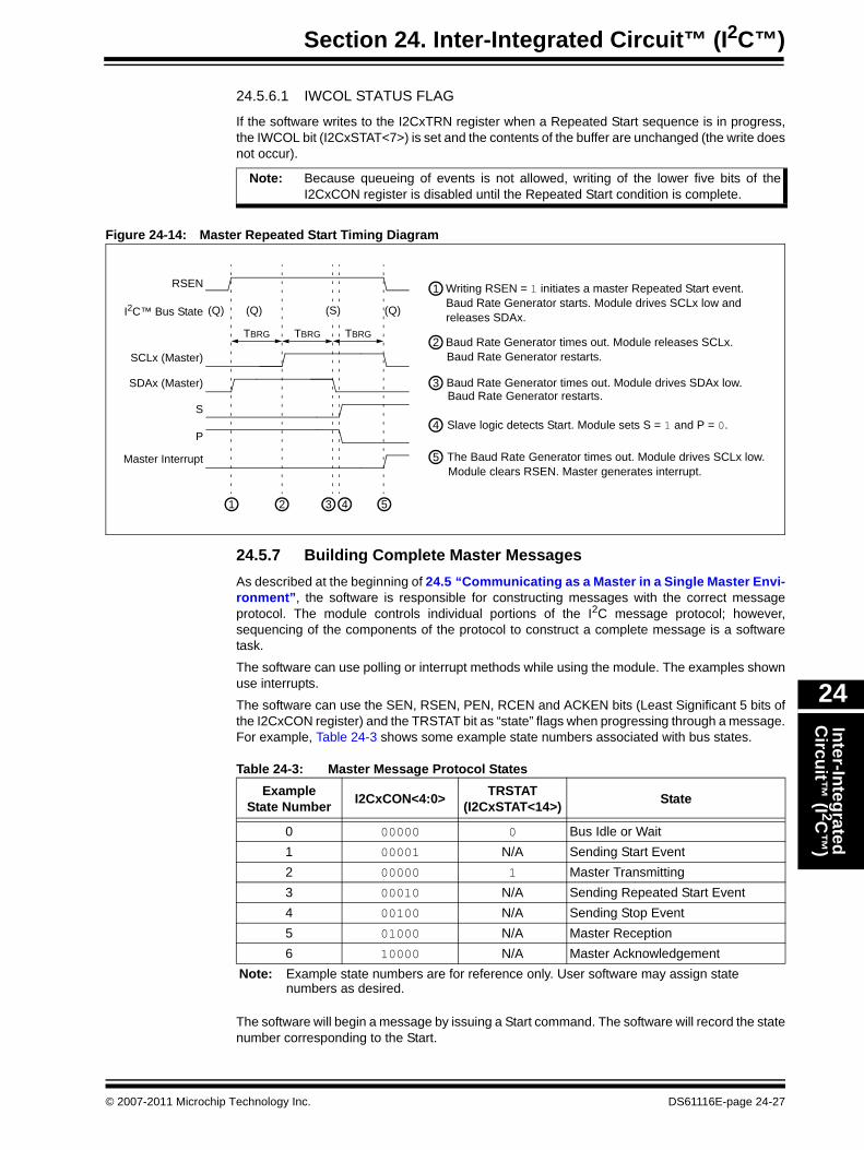
24.5.6 Generating a Repeated Start Bus EventSetting the Repeated Start Enable bit, RSEN (I2CxCON<1>), enables generation of a master Repeated Start sequence (see Figure 24-14).
To generate a Repeated Start condition, software sets the RSEN bit (I2CxCON<1>). The module asserts the SCLx pin low. When the module samples the SCLx pin low, the module releases the SDAx pin for one BRG count (TBRG). When the BRG times out and the module samples SDAx high, the module deasserts the SCLx pin. When the module samples the SCLx pin high, the BRG reloads and begins counting. SDAx and SCLx must be sampled high for one TBRG. This action is then followed by assertion of the SDAx pin low for one TBRG while SCLx is high.
The following is the Repeated Start sequence:
1. The slave detects the Start condition, sets the S bit (I2CxSTAT<3>) and clears the P bit (I2CxSTAT<4>).
2. The RSEN bit is automatically cleared.3. The module generates the master interrupt.
Note: The lower five bits of the I2CxCON register must be ‘0’ (master logic inactive) before attempting to set the PEN bit.
Note: Because queueing of events is not allowed, writing to the lower 5 bits of the I2CxCON register is disabled until the Stop condition is complete.
SCLx (Master)
SDAx (Master)
S
PEN
Master Interrupt
TBRG
1 2 3 5
Writing PEN = 1 initiates a master Stop event. 1
TBRG
Baud Rate Generator starts. Module drives SDAx low.
Baud Rate Generator times out. Module releases SCLx. 2Baud Rate Generator restarts.
Baud Rate Generator times out. Module releases SDAx.3
Slave logic detects Stop. Module sets P = 1, S = 0.4
I2C™ Bus State (I)
P
TBRG
(Q)
4
Baud Rate Generator restarts.
The Baud Rate Generator times out. Module clears PEN. 5Master generates interrupt.
(Q) (P)
Note: The lower 5 bits of I2CxCON must be ‘0’ (master logic inactive) before attempting to set the RSEN bit.
DS61116E-page 24-26 © 2007-2011 Microchip Technology Inc.
Section 24. Inter-Integrated Circuit™ (I2C™)Inter-Integrated C
ircuit™ (I 2C
™)
24
24.5.6.1 IWCOL STATUS FLAG
If the software writes to the I2CxTRN register when a Repeated Start sequence is in progress, the IWCOL bit (I2CxSTAT<7>) is set and the contents of the buffer are unchanged (the write doesnot occur).
Figure 24-14: Master Repeated Start Timing Diagram
24.5.7 Building Complete Master MessagesAs described at the beginning of 24.5 “Communicating as a Master in a Single Master Envi-ronment”, the software is responsible for constructing messages with the correct message protocol. The module controls individual portions of the I2C message protocol; however, sequencing of the components of the protocol to construct a complete message is a software task.
The software can use polling or interrupt methods while using the module. The examples shown use interrupts.
The software can use the SEN, RSEN, PEN, RCEN and ACKEN bits (Least Significant 5 bits of the I2CxCON register) and the TRSTAT bit as “state” flags when progressing through a message. For example, Table 24-3 shows some example state numbers associated with bus states.
The software will begin a message by issuing a Start command. The software will record the state number corresponding to the Start.
Note: Because queueing of events is not allowed, writing of the lower five bits of the I2CxCON register is disabled until the Repeated Start condition is complete.
SCLx (Master)
SDAx (Master)
S
RSEN
Master Interrupt
TBRG
1 2 3 5
Writing RSEN = 1 initiates a master Repeated Start event. 1
TBRG
Baud Rate Generator starts. Module drives SCLx low and
Baud Rate Generator times out. Module releases SCLx. 2Baud Rate Generator restarts.
Baud Rate Generator times out. Module drives SDAx low.3
Slave logic detects Start. Module sets S = 1 and P = 0.4
I2C™ Bus State (Q)
P
TBRG
(Q)
4
Baud Rate Generator restarts.
The Baud Rate Generator times out. Module drives SCLx low.5Module clears RSEN. Master generates interrupt.
(Q) releases SDAx.(S)
Table 24-3: Master Message Protocol StatesExample
State Number I2CxCON<4:0> TRSTAT(I2CxSTAT<14>) State
0 00000 0 Bus Idle or Wait1 00001 N/A Sending Start Event2 00000 1 Master Transmitting3 00010 N/A Sending Repeated Start Event4 00100 N/A Sending Stop Event5 01000 N/A Master Reception6 10000 N/A Master Acknowledgement
Note: Example state numbers are for reference only. User software may assign state numbers as desired.
© 2007-2011 Microchip Technology Inc. DS61116E-page 24-27
PIC32 Family Reference Manual
As each event completes and generates an interrupt, the interrupt handler may check the state number. So, for a Start state, the interrupt handler will confirm execution of the Start sequence and then start a master transmission event to send the I2C device address, changing the state number to correspond to the master transmission.
On the next interrupt, the interrupt handler will again check the state, determining that a master transmission just completed. The interrupt handler will confirm successful transmission of the data, then move on to the next event, depending on the contents of the message. In this manner, on each interrupt, the interrupt handler will progress through the message protocol until the complete message is sent.
Figure 24-15 provides a more detailed examination of the same message sequence shown in Figure 24-7. Figure 24-16 shows some simple examples of messages using 7-bit addressing format. Figure 24-17 shows an example of a 10-bit addressing format message sending data to a slave. Figure 24-18 shows an example of a 10-bit addressing format message receiving data from a slave.
DS61116E-page 24-28 © 2007-2011 Microchip Technology Inc.
© 2007-2011 M
icrochip Technology Inc.D
S61116E
-page 24-29
Section 24. Inter-Integrated Circuit™
(I 2C™
)
F
1 2 3 4 5 6 7 8
D3 D2 D1 D0D7 D6 D5 D4
9
N
7 8 9
master transmission. The data is a resend of
eception. On interrupt, the software reads
wledge event. ACKDT = 0 to send NACK.
op event.
yte, but with R/W bit set, indicating a read.
e RBF flag.
Inter-Integrated Circuit™ (I2C™) 24
igure 24-15: Master Message (Typical I2C™ Message: Read of Serial EEPROM)
1 Setting the SEN bit starts a Start event.
ACKDT
ACKEN
SEN
SCLx
SDAx
SCLx
SDAx
I2CxTRN
TBF
I2CxRCV
RBF
Master
ACKSTAT
1 2 3 4 5 6 7 8
A1 A0
9
A
PEN
RCEN
1 2 3 4 5 6 7 8
A11
A10
A9
A8
1 2 3 4 5 6 7 8 9
W1 1
RSEN
1 2 3 4 5 6 7 8 9
1 32
9
AAA
4 5
2 Writing the I2CxTRN register starts a master transmission. The data is the serial
3 Writing the I2CxTRN register starts a master transmission. The data is the first
4 -
5
Writing the I2CxTRN register starts a 6
Setting the RCEN bit starts a master r7
9
Setting the ACKEN bit starts an Ackno
Setting the PEN bit starts a master St
EEPROM device address byte, with R/W clear, indicating a write.
byte of the EEPROM data address.
the serial EEPROM device address b
the I2CxRCV register, which clears th
0 0 A2 A7 A6 A5 A4 A2 A1 A0 A1 A0 R1 10 0 A20 0 0 0
6
Writing the I2CxTRN register starts a master transmission. The data is the secondbyte of the EEPROM data address.
8
Setting the RSEN bit starts a Repeated Start event.
(Master)
(Master)
(Slave)
(Slave)
A3
Master interrupt cleared
Interrupt by user software.

PIC32 Fam
ily Reference M
anual
DS
61116E-page 24-30
© 2007-2011 M
icrochip Technology Inc.
1 2 3 4 5 6 7 8
D3 D2 D1 D0D7 D6 D5 D4
9
N
97 8
s a master transmission. The data is the
ter reception.
cknowledge event. ACKDT = 0 to send NACK.
r Stop event.
Figure 24-16: Master Message (7-bit Address: Transmission and Reception)
1 Setting the SEN bit starts a Start event.
ACKDT
ACKEN
SEN
SCLx
SDAx
SCLx
SDAx
I2CxTRN
TBF
I2CxRCV
RBF
Master
ACKSTAT
1 2 3 4 5 6 7 8
A2 A1
9
A
PEN
RCEN
1 2 3 4 5 6 7 8
D7 D6 D5 D4 D3 D2 D1 D0
1 2 3 4 5 6 7 8 9
W
RSEN
1 32
9
A
4 5 6
2 Writing the I2CxTRN register starts a master transmission. The data is the
3 Writing the I2CxTRN register starts a master transmission. The data is the
4 Setting the PEN bit starts a master Stop event.
5 Setting the SEN bit starts a Start event.
6 Writing the I2CxTRN register start
7 Setting the RCEN bit starts a mas
8 Setting the ACKEN bit starts an A
Setting the PEN bit starts a maste
address byte with R/W bit clear.
message byte.
A7 A6 A5 A4 A3
A
A2 A1 RA7 A6 A5 A4 A3
address byte with R/W bit set.
9
(Master)
(Master)
(Slave)
(Slave)
Master interrupt cleared
Interrupt by user software.
© 2007-2011 M
icrochip Technology Inc.D
S61116E
-page 24-31
Section 24. Inter-Integrated Circuit™
(I 2C™
)
F
1 2 3 4 5 6 7 8 9
7
op event.
D3 D2 D1 D0D7 D6 D5 D4
A
master transmission. The data is the second
master transmission. The data is the third
Inter-Integrated Circuit™ (I2C™) 24
igure 24-17: Master Message (10-bit Transmission)
1 Setting the SEN bit starts a Start event.
ACKDT
ACKEN
SEN
SCLx
SDAx
SCLx
SDAx
I2CxTRN
TBF
I2CxRCV
RBF
Master
ACKSTAT
1 2 3 4 5 6 7 8
A9 A8
9
A
PEN
RCEN
1 2 3 4 5 6 7 8
D3 D2 D1 D0D7 D6 D5 D4A7 A6 A5 A4 A3 A2 A1 A0
1 2 3 4 5 6 7 8 9
W01 1 1 1
RSEN
1 2 3 4 5 6 7 8 9
1 32
9
AAA
4 5 6
2 Writing the I2CxTRN register starts a master transmission. The data is the first
3 Writing the I2CxTRN register starts a master transmission. The data is the second
4 Writing the I2CxTRN register starts a master transmission. The data is the first
Setting the PEN bit starts a master St
byte of the address.
byte of the address.
byte of the message data.
D3 D2 D1 D0D7 D6 D5 D4
5 Writing the I2CxTRN register starts abyte of the message data.
6 Writing the I2CxTRN register starts abyte of the message data.
7
(Master)
(Master)
(Slave)
(Slave)
Master interrupt cleared
Interrupt by user software.
PIC32 Fam
ily Reference M
anual
DS
61116E-page 24-32
© 2007-2011 M
icrochip Technology Inc.
9
A
1 2 3 4 5 6 7 8
D3 D2 D1 D0D7 D6 D5 D4
9
N
8 9 10
ter reception. On interrupt, the software reads
cknowledge event. ACKDT = 1 to send ACK.
ter reception.
cknowledge event. ACKDT = 0 to send NACK.
r Stop event.
s the RBF flag.
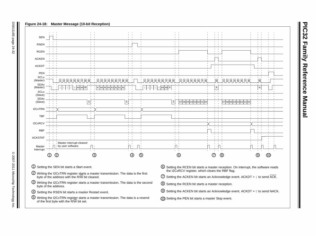
Figure 24-18: Master Message (10-bit Reception)
1 Setting the SEN bit starts a Start event.
ACKDT
ACKEN
SEN
SCLx
SDAx
SCLx
SDAx
I2CxTRN
TBF
I2CxRCV
RBF
Master
ACKSTAT
1 2 3 4 5 6 7 8
A9 A8
9
A
PEN
RCEN
1 2 3 4 5 6 7 8
D3 D2 D1 D0D7 D6 D5 D4
A7 A6 A5 A4 A3 A2 A1 A0
1 2 3 4 5 6 7 8 9
W01 1 1 1
RSEN
A9 A801 1 1 1 R
1 2 3 4 5 6 7 8 9
1 32
AA
4 5 6 7
2 Writing the I2CxTRN register starts a master transmission. The data is the first
3 Writing the I2CxTRN register starts a master transmission. The data is the second
4 Setting the RSEN bit starts a master Restart event.5 Writing the I2CxTRN register starts a master transmission. The data is a resend
6 Setting the RCEN bit starts a mas
7 Setting the ACKEN bit starts an A
8 Setting the RCEN bit starts a mas
9 Setting the ACKEN bit starts an A
Setting the PEN bit starts a maste
byte of the address with the R/W bit cleared.
byte of the address.
of the first byte with the R/W bit set.
the I2CxRCV register, which clear
(Slave)
(Slave)
(Master)
(Master)
Master interrupt cleared
10
Interruptby user software.
Section 24. Inter-Integrated Circuit™ (I2C™)Inter-Integrated C
ircuit™ (I 2C
™)
24
24.6 COMMUNICATING AS A MASTER IN A MULTI-MASTER ENVIRONMENTThe I2C protocol allows for more than one master to be attached to a system bus. Taking into account that a master can initiate message transactions and generate clocks for the bus, the pro-tocol has methods to account for situations where more than one master is attempting to control the bus. Clock synchronization ensures that multiple nodes can synchronize their SCLx clocks to result in one common clock on the SCLx line. Bus arbitration ensures that if more than one node attempts a message transaction, one node, and only one node, will be successful in completing the message. The other nodes will lose bus arbitration and be left with a bus collision.
24.6.1 Multi-Master OperationThe master module has no special settings to enable multi-master operation. The module per-forms clock synchronization and bus arbitration at all times. If the module is used in a single mas-ter environment, clock synchronization will only occur between the master and slaves, and bus arbitration will not occur.
24.6.2 Master Clock SynchronizationIn a multi-master system, different masters may have different baud rates. Clock synchronization will ensure that when these masters are attempting to arbitrate the bus, their clocks will be coordinated.
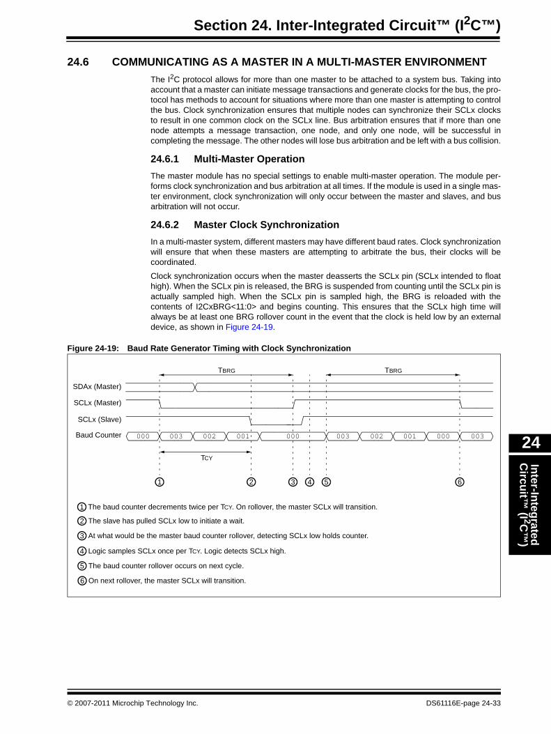
Clock synchronization occurs when the master deasserts the SCLx pin (SCLx intended to float high). When the SCLx pin is released, the BRG is suspended from counting until the SCLx pin is actually sampled high. When the SCLx pin is sampled high, the BRG is reloaded with the contents of I2CxBRG<11:0> and begins counting. This ensures that the SCLx high time will always be at least one BRG rollover count in the event that the clock is held low by an external device, as shown in Figure 24-19.
Figure 24-19: Baud Rate Generator Timing with Clock Synchronization
SCLx (Slave)
The baud counter decrements twice per TCY. On rollover, the master SCLx will transition.1
1
000 003001002003
SCLx (Master)
001002003000Baud Counter
SDAx (Master)
3 4 6
The slave has pulled SCLx low to initiate a wait.2
At what would be the master baud counter rollover, detecting SCLx low holds counter.3
Logic samples SCLx once per TCY. Logic detects SCLx high.4
2
The baud counter rollover occurs on next cycle.5
5
On next rollover, the master SCLx will transition.6
TBRG TBRG
TCY
000
© 2007-2011 Microchip Technology Inc. DS61116E-page 24-33
PIC32 Family Reference Manual
24.6.3 Bus Arbitration and Bus CollisionBus arbitration supports multi-master system operation.
The wired AND nature of the SDAx line permits arbitration. Arbitration takes place when the first master outputs a ‘1’ on SDAx by letting SDAx float high and simultaneously, the second master outputs a ‘0’ on SDAx by pulling SDAx low. The SDAx signal will go low. In this case, the second master has won bus arbitration. The first master has lost bus arbitration, and therefore, has a bus collision.
For the first master, the expected data on SDAx is a ‘1’, yet the data sampled on SDAx is a ‘0’. This is the definition of a bus collision.
The first master will set the Bus Collision bit, BCL (I2CxSTAT<10>), and generate a bus collision interrupt. The master module will reset the I2C port to its Idle state.
In multi-master operation, the SDAx line must be monitored for arbitration to see if the signal level is the expected output level. This check is performed by the master module, with the result placed in the BCL bit.
The states where arbitration can be lost are:
• A Start condition• A Repeated Start condition• Address, Data or Acknowledge bit• A Stop condition
24.6.4 Detecting Bus Collisions and Resending MessagesWhen a bus collision occurs, the module sets the BCL bit and generates a bus collision interrupt. If bus collision occurs during a byte transmission, the transmission is halted, the TBF bit (I2CxSTAT<0>) is cleared and the SDAx and SCLx pins are deasserted. If bus collision occurs during a Start, Repeated Start, Stop or Acknowledge condition, the condition is aborted, the respective control bits in the I2CxCON register are cleared and the SDAx and SCLx lines are deasserted.
The software is expecting an interrupt at the completion of the master event. The software can check the BCL bit to determine if the master event completed successfully or a collision occurred. If a collision occurs, the software must abort sending the rest of the pending message and pre-pare to resend the entire message sequence, beginning with the Start condition, after the bus returns to an Idle state. The software can monitor the S (I2CxSTAT<3>) and P bits (I2CxSTAT<4>) to wait for an Idle bus. When the software services the bus collision Interrupt Ser-vice Routine and the I2C bus is free, the software can resume communication by asserting a Start condition.
24.6.5 Bus Collision During a Start ConditionBefore issuing a Start command, the software should verify an Idle state of the bus using the S and P Status bits. Two masters may attempt to initiate a message at a similar point in time. Typ-ically, the masters will synchronize clocks and continue arbitration into the message until one loses arbitration. However, certain conditions can cause a bus collision to occur during a Start. In this case, the master that loses arbitration during the Start (S) bit generates a bus collision interrupt.
24.6.6 Bus Collision During a Repeated Start ConditionShould two masters not collide throughout an address byte, a bus collision may occur when one master attempts to assert a Repeated Start while another transmits data. In this case, the master generating the Repeated Start will lose arbitration and generate a bus collision interrupt.
DS61116E-page 24-34 © 2007-2011 Microchip Technology Inc.
Section 24. Inter-Integrated Circuit™ (I2C™)Inter-Integrated C
ircuit™ (I 2C
™)
24
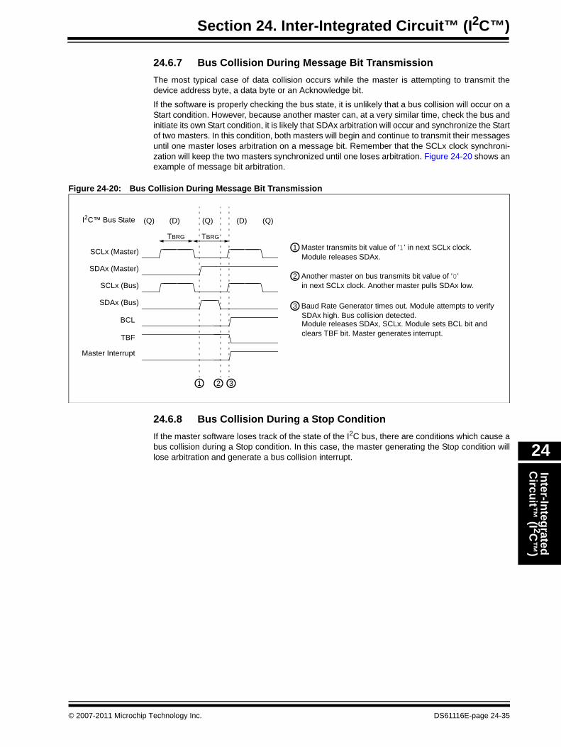
24.6.7 Bus Collision During Message Bit TransmissionThe most typical case of data collision occurs while the master is attempting to transmit the device address byte, a data byte or an Acknowledge bit.
If the software is properly checking the bus state, it is unlikely that a bus collision will occur on a Start condition. However, because another master can, at a very similar time, check the bus and initiate its own Start condition, it is likely that SDAx arbitration will occur and synchronize the Start of two masters. In this condition, both masters will begin and continue to transmit their messages until one master loses arbitration on a message bit. Remember that the SCLx clock synchroni-zation will keep the two masters synchronized until one loses arbitration. Figure 24-20 shows an example of message bit arbitration.
Figure 24-20: Bus Collision During Message Bit Transmission
24.6.8 Bus Collision During a Stop ConditionIf the master software loses track of the state of the I2C bus, there are conditions which cause a bus collision during a Stop condition. In this case, the master generating the Stop condition will lose arbitration and generate a bus collision interrupt.
SCLx (Master)
SDAx (Master)
TBF
TBRG
1 2 3
Master transmits bit value of ‘1’ in next SCLx clock.1TBRG
Module releases SDAx.
Another master on bus transmits bit value of ‘0’ 2in next SCLx clock. Another master pulls SDAx low.
Baud Rate Generator times out. Module attempts to verify3
I2C™ Bus State
BCL
(D)
SCLx (Bus)
SDAx (Bus)
SDAx high. Bus collision detected.Module releases SDAx, SCLx. Module sets BCL bit andclears TBF bit. Master generates interrupt.
(D)(Q)(Q) (Q)
Master Interrupt
© 2007-2011 Microchip Technology Inc. DS61116E-page 24-35
PIC32 Family Reference Manual
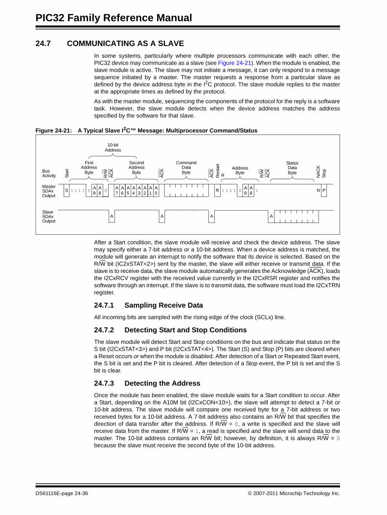
24.7 COMMUNICATING AS A SLAVEIn some systems, particularly where multiple processors communicate with each other, the PIC32 device may communicate as a slave (see Figure 24-21). When the module is enabled, the slave module is active. The slave may not initiate a message, it can only respond to a message sequence initiated by a master. The master requests a response from a particular slave as defined by the device address byte in the I2C protocol. The slave module replies to the master at the appropriate times as defined by the protocol.
As with the master module, sequencing the components of the protocol for the reply is a software task. However, the slave module detects when the device address matches the address specified by the software for that slave.
Figure 24-21: A Typical Slave I2C™ Message: Multiprocessor Command/Status
After a Start condition, the slave module will receive and check the device address. The slave may specify either a 7-bit address or a 10-bit address. When a device address is matched, the module will generate an interrupt to notify the software that its device is selected. Based on the R/W bit (IC2xSTAT<2>) sent by the master, the slave will either receive or transmit data. If the slave is to receive data, the slave module automatically generates the Acknowledge (ACK), loads the I2CxRCV register with the received value currently in the I2CxRSR register and notifies the software through an interrupt. If the slave is to transmit data, the software must load the I2CxTRN register.
24.7.1 Sampling Receive DataAll incoming bits are sampled with the rising edge of the clock (SCLx) line.
24.7.2 Detecting Start and Stop ConditionsThe slave module will detect Start and Stop conditions on the bus and indicate that status on the S bit (I2CxSTAT<3>) and P bit (I2CxSTAT<4>). The Start (S) and Stop (P) bits are cleared when a Reset occurs or when the module is disabled. After detection of a Start or Repeated Start event, the S bit is set and the P bit is cleared. After detection of a Stop event, the P bit is set and the S bit is clear.
24.7.3 Detecting the AddressOnce the module has been enabled, the slave module waits for a Start condition to occur. After a Start, depending on the A10M bit (I2CxCON<10>), the slave will attempt to detect a 7-bit or 10-bit address. The slave module will compare one received byte for a 7-bit address or two received bytes for a 10-bit address. A 7-bit address also contains an R/W bit that specifies the direction of data transfer after the address. If R/W = 0, a write is specified and the slave will receive data from the master. If R/W = 1, a read is specified and the slave will send data to the master. The 10-bit address contains an R/W bit; however, by definition, it is always R/W = 0because the slave must receive the second byte of the 10-bit address.
Bus
MasterSDAx
Star
t
FirstAddress Address
Byte
S 1 1 1 0 A A 09 8 R P
SlaveSDAx
Activity
N
AAAA
Output
Output
R/W
ACK
ACK
ACK
Res
tart
R/W
ACK
NAC
KSt
op
1
Byte
SecondAddress
Byte
A A7 6
A A5 4
A A3 2
A A1 0
CommandDataByte
1 1 1 0 A A 19 81
StatusDataByte
10-bitAddress
R
DS61116E-page 24-36 © 2007-2011 Microchip Technology Inc.
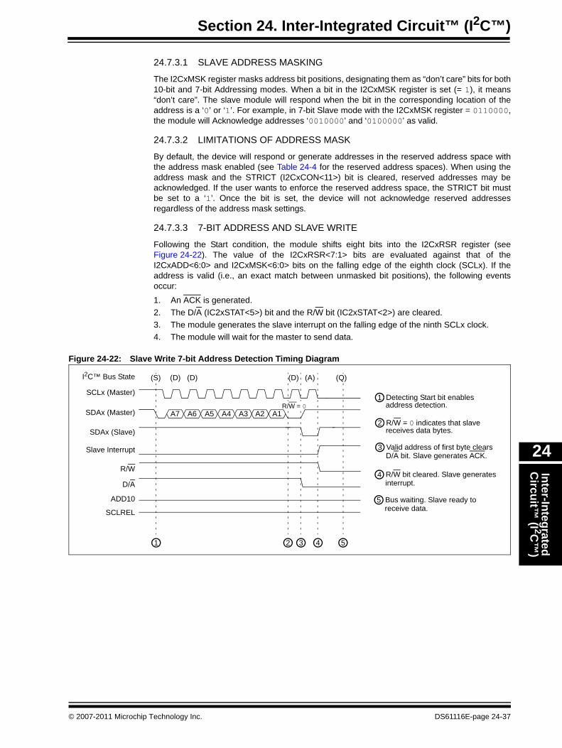
Section 24. Inter-Integrated Circuit™ (I2C™)Inter-Integrated C
ircuit™ (I 2C
™)
24
24.7.3.1 SLAVE ADDRESS MASKING
The I2CxMSK register masks address bit positions, designating them as “don’t care” bits for both 10-bit and 7-bit Addressing modes. When a bit in the I2CxMSK register is set (= 1), it means “don’t care”. The slave module will respond when the bit in the corresponding location of the address is a ‘0’ or ‘1’. For example, in 7-bit Slave mode with the I2CxMSK register = 0110000, the module will Acknowledge addresses ‘0010000’ and ‘0100000’ as valid.
24.7.3.2 LIMITATIONS OF ADDRESS MASK
By default, the device will respond or generate addresses in the reserved address space with the address mask enabled (see Table 24-4 for the reserved address spaces). When using the address mask and the STRICT (I2CxCON<11>) bit is cleared, reserved addresses may be acknowledged. If the user wants to enforce the reserved address space, the STRICT bit must be set to a ‘1’. Once the bit is set, the device will not acknowledge reserved addresses regardless of the address mask settings.
24.7.3.3 7-BIT ADDRESS AND SLAVE WRITE
Following the Start condition, the module shifts eight bits into the I2CxRSR register (see Figure 24-22). The value of the I2CxRSR<7:1> bits are evaluated against that of the I2CxADD<6:0> and I2CxMSK<6:0> bits on the falling edge of the eighth clock (SCLx). If the address is valid (i.e., an exact match between unmasked bit positions), the following events occur:
1. An ACK is generated.2. The D/A (IC2xSTAT<5>) bit and the R/W bit (IC2xSTAT<2>) are cleared.3. The module generates the slave interrupt on the falling edge of the ninth SCLx clock.4. The module will wait for the master to send data.
Figure 24-22: Slave Write 7-bit Address Detection Timing Diagram
SCLx (Master)
SDAx (Master)
SDAx (Slave)
Slave Interrupt
3 41 2
Detecting Start bit enables1
I2C™ Bus State (D) (D) (A)(D)
A5A6A7 A4 A3 A2 A1
D/A
ADD10
SCLREL
R/W
address detection.
R/W = 0 indicates that slave 2receives data bytes.
Valid address of first byte clears 3D/A bit. Slave generates ACK.
R/W bit cleared. Slave generates 4interrupt.
5
Bus waiting. Slave ready to 5receive data.
R/W = 0
(S) (Q)
© 2007-2011 Microchip Technology Inc. DS61116E-page 24-37
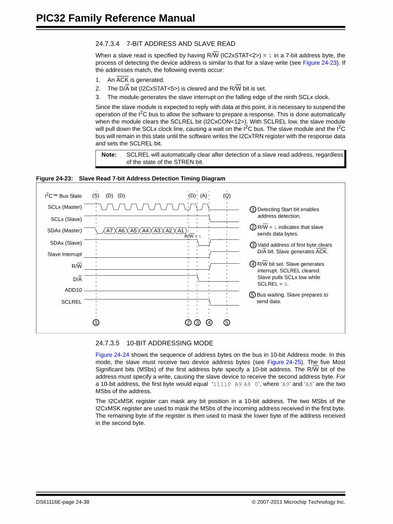
PIC32 Family Reference Manual
24.7.3.4 7-BIT ADDRESS AND SLAVE READ
When a slave read is specified by having R/W (IC2xSTAT<2>) = 1 in a 7-bit address byte, the process of detecting the device address is similar to that for a slave write (see Figure 24-23). If the addresses match, the following events occur:
1. An ACK is generated.2. The D/A bit (I2CxSTAT<5>) is cleared and the R/W bit is set.3. The module generates the slave interrupt on the falling edge of the ninth SCLx clock.
Since the slave module is expected to reply with data at this point, it is necessary to suspend the operation of the I2C bus to allow the software to prepare a response. This is done automatically when the module clears the SCLREL bit (I2CxCON<12>). With SCLREL low, the slave module will pull down the SCLx clock line, causing a wait on the I2C bus. The slave module and the I2C bus will remain in this state until the software writes the I2CxTRN register with the response data and sets the SCLREL bit.
Figure 24-23: Slave Read 7-bit Address Detection Timing Diagram
24.7.3.5 10-BIT ADDRESSING MODE
Figure 24-24 shows the sequence of address bytes on the bus in 10-bit Address mode. In this mode, the slave must receive two device address bytes (see Figure 24-25). The five Most Significant bits (MSbs) of the first address byte specify a 10-bit address. The R/W bit of the address must specify a write, causing the slave device to receive the second address byte. For a 10-bit address, the first byte would equal ‘11110 A9 A8 0’, where ‘A9’ and ‘A8’ are the two MSbs of the address.
The I2CxMSK register can mask any bit position in a 10-bit address. The two MSbs of the I2CxMSK register are used to mask the MSbs of the incoming address received in the first byte. The remaining byte of the register is then used to mask the lower byte of the address received in the second byte.
Note: SCLREL will automatically clear after detection of a slave read address, regardless of the state of the STREN bit.
SCLx (Master)
SDAx (Master)
SDAx (Slave)
Slave Interrupt
3 41 2
Detecting Start bit enables1
I2C™ Bus State (D) (D) (A)(D)
A5A6A7 A4 A3 A2 A1
D/A
ADD10
SCLREL
R/W
address detection.
R/W = 1 indicates that slave 2sends data bytes.
Valid address of first byte clears 3D/A bit. Slave generates ACK.
R/W bit set. Slave generates 4interrupt. SCLREL cleared.
5
Bus waiting. Slave prepares to 5send data.
SCLx (Slave)
Slave pulls SCLx low whileSCLREL = 0.
(S) (Q)
R/W = 1
DS61116E-page 24-38 © 2007-2011 Microchip Technology Inc.

Section 24. Inter-Integrated Circuit™ (I2C™)Inter-Integrated C
ircuit™ (I 2C
™)
24
Following the Start condition, the module shifts eight bits into the I2CxRSR register. The value of the I2CxRSR<2:1> bits are evaluated against the value of the I2CxADD<9:8> and I2CxMSK<9:8> bits, while the value of the I2CxRSR<7:3> bits are compared to ‘11110’. Address evaluation occurs on the falling edge of the eighth clock (SCLx). For the address to be valid, the I2CxRSR<7:3> bits must equal ‘11110’, while the I2CxRSR<2:1> bits must exactly match any unmasked bits in the I2CxADD<9:8> bits. (If both bits are masked, a match is not needed.) If the address is valid, the following events occur:
1. An ACK is generated.2. The D/A (I2CxSTAT<5>) bit and the R/W bit (IC2xSTAT<2>) are cleared.3. The module generates the slave interrupt on the falling edge of the ninth SCLx clock.
The module does generate an interrupt after the reception of the first byte of a 10-bit address; however, this interrupt is of little use.
The module will continue to receive the second byte into the I2CxRSR register. This time, the I2CxRSR<7:0> bits are evaluated against the I2CADD<7:0> and I2CxMSK<7:0> bits. If the lower byte of the address is valid as previously described, the following events occur:
1. An ACK is generated.2. The ADD10 bit (I2CxSTAT<8>) is set.3. The module generates the slave interrupt on the falling edge of the ninth SCLx clock.4. The module will wait for the master to send data or initiate a Repeated Start condition.
Figure 24-24: 10-bit Address Sequence
Figure 24-25: 10-bit Address Detection Timing Diagram
Note: Following a Repeated Start condition in 10-bit Addressing mode, the slave module only matches the first 7-bit address, ‘11110 A9 A8 0’.
s 1 1 1 1 0 A9 A8 R/WACKA7 A6 A5 A4 A3 A2 A1 A0 ACK
= 0 for writesent by slave
SCLx (Master)
SDAx (Master)
SDAx (Slave)
Slave Interrupt
2 4 51 3
Detecting Start bit enables address detection.1
Address match of first byte clears D/A bit and causes slave logic to generate ACK.2
Reception of first byte clears R/W bit. Slave logic generates interrupt.3
Address match of first and second byte sets ADD10 and causes slave logic to generate ACK.4
Reception of second byte completes 10-bit address. Slave logic generates interrupt.5
I2C™ Bus State (D) (D) (A)(D)
111 1 0 A9 A8R/W = 0
D/A
ADD10
SCLREL
A5A6A7 A4 A3 A2 A1 A0
R/W
(D) (D) (A)(D)
6
Bus waiting. Slave ready to receive data.5
(S) (Q)
© 2007-2011 Microchip Technology Inc. DS61116E-page 24-39
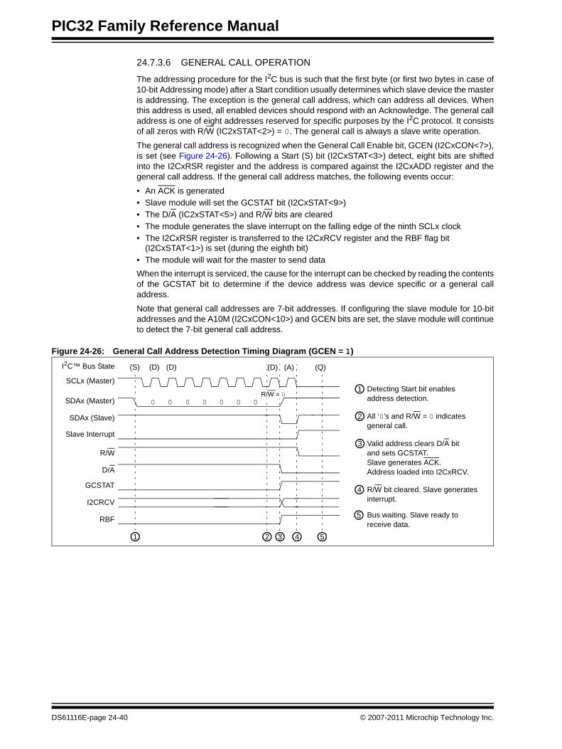
PIC32 Family Reference Manual
24.7.3.6 GENERAL CALL OPERATION
The addressing procedure for the I2C bus is such that the first byte (or first two bytes in case of 10-bit Addressing mode) after a Start condition usually determines which slave device the master is addressing. The exception is the general call address, which can address all devices. When this address is used, all enabled devices should respond with an Acknowledge. The general call address is one of eight addresses reserved for specific purposes by the I2C protocol. It consists of all zeros with R/W (IC2xSTAT<2>) = 0. The general call is always a slave write operation.
The general call address is recognized when the General Call Enable bit, GCEN (I2CxCON<7>), is set (see Figure 24-26). Following a Start (S) bit (I2CxSTAT<3>) detect, eight bits are shifted into the I2CxRSR register and the address is compared against the I2CxADD register and the general call address. If the general call address matches, the following events occur:
• An ACK is generated• Slave module will set the GCSTAT bit (I2CxSTAT<9>)• The D/A (IC2xSTAT<5>) and R/W bits are cleared• The module generates the slave interrupt on the falling edge of the ninth SCLx clock• The I2CxRSR register is transferred to the I2CxRCV register and the RBF flag bit
(I2CxSTAT<1>) is set (during the eighth bit)• The module will wait for the master to send dataWhen the interrupt is serviced, the cause for the interrupt can be checked by reading the contents of the GCSTAT bit to determine if the device address was device specific or a general call address.
Note that general call addresses are 7-bit addresses. If configuring the slave module for 10-bit addresses and the A10M (I2CxCON<10>) and GCEN bits are set, the slave module will continue to detect the 7-bit general call address.
Figure 24-26: General Call Address Detection Timing Diagram (GCEN = 1)
SCLx (Master)
SDAx (Master)
SDAx (Slave)
Slave Interrupt
3 41 2
Detecting Start bit enables1
I2C™ Bus State (D) (D) (A)(D)
000 0 0 0 0
D/A
I2CRCV
RBF
R/W
address detection.
All ‘0’s and R/W = 0 indicates2general call.
Valid address clears D/A bit3and sets GCSTAT.
R/W bit cleared. Slave generates 4interrupt.
5
Bus waiting. Slave ready to 5receive data.
GCSTAT
Slave generates ACK.Address loaded into I2CxRCV.
R/W = 0
(S) (Q)
DS61116E-page 24-40 © 2007-2011 Microchip Technology Inc.
Section 24. Inter-Integrated Circuit™ (I2C™)Inter-Integrated C
ircuit™ (I 2C
™)
24
24.7.3.7 STRICT ADDRESS SUPPORT
When the STRICT Control bit (I2CxCON<11>) is set, it enables the module to enforce all reserved addressing and will not acknowledge any addresses if they fall within the reserved address table.
24.7.3.8 WHEN AN ADDRESS IS INVALID
If a 7-bit address does not match the contents of the I2CxADD<6:0> bits, the slave module will return to an Idle state and ignore all bus activity until after the Stop condition.
If the first byte of a 10-bit address does not match the contents of the I2CxADD<9:8> bits, the slave module will return to an Idle state and ignore all bus activity until after the Stop condition.
If the first byte of a 10-bit address matches the contents of the I2CxADD<9:8> bits, but the sec-ond byte of the 10-bit address does not match the I2CxADD<7:0> bits, the slave module will return to an Idle state and ignore all bus activity until after the Stop condition.
24.7.3.9 ADDRESSES RESERVED FROM MASKING
Even when enabled, there are several addresses that are excluded in hardware from masking. For these addresses, an Acknowledge will not be issued independent of the mask setting. These addresses are listed in Table 24-4.
24.7.4 Receiving Data from a Master DeviceWhen the R/W bit of the device address byte is zero and an address match occurs, the R/W bit is cleared. The slave module enters a state waiting for data to be sent by the master. After the device address byte, the contents of the data byte are defined by the system protocol and are only received by the slave module.
The slave module shifts eight bits into the I2CxRSR register. On the falling edge of the eighth clock (SCLx), the following events occur:
1. The module begins to generate an ACK or NACK.2. The RBF bit (I2CxSTAT<1>) is set to indicate received data.3. The I2CxRSR register byte is transferred to the I2CxRCV register for access by the
software.4. The D/A bit (I2CxSTAT<5>) is set.5. A slave interrupt is generated. Software may check the status of the I2CxSTAT register to
determine the cause of the event, and then clear the slave interrupt flag.6. The module will wait for the next data byte.
Table 24-4: Reserved I2C™ Bus Addresses(1)
7-bit Address Mode:
Slave Address R/W bit (IC2xSTAT<2>) Description
0000 000 0 General Call Address(1)
0000 000 1 Start Byte0000 001 x CBUS Address0000 010 x Reserved0000 011 x Reserved0000 1xx x HS Mode Master Code1111 1xx x Reserved1111 0xx x 10-bit Slave Upper Byte(2)
Note 1: Address will be Acknowledged only if GCEN (I2CxCON<7>) = 1.2: Match on this address can only occur as the upper byte in the 10-bit Addressing mode.
© 2007-2011 Microchip Technology Inc. DS61116E-page 24-41
PIC32 Family Reference Manual
24.7.4.1 ACKNOWLEDGE GENERATION
Normally, the slave module will Acknowledge all received bytes by sending an ACK on the ninth SCLx clock. If the receive buffer is overrun, the slave module does not generate this ACK. Overrun is indicated if either (or both):
• The buffer full bit, RBF (I2CxSTAT<1>), was set before the transfer was received• The overflow bit, I2COV (I2CxSTAT<6>), was set before the transfer was received
Table 24-5 shows what happens when a data transfer byte is received, given the status of the RBF and I2COV bits. If the RBF bit is already set when the slave module attempts to transfer to the I2CxRCV register, the transfer does not occur but the interrupt is generated and the I2COV bit is set. If both the RBF and I2COV bits are set, the slave module acts similarly. The shaded cells show the condition where software did not properly clear the overflow condition.
Reading the I2CxRCV register clears the RBF bit. The I2COV bit is cleared by writing to a ‘0’ through software.
24.7.4.2 WAIT STATES DURING SLAVE RECEPTIONS
When the slave module receives a data byte, the master can potentially begin sending the next byte immediately. This allows the software controlling the slave module nine SCLx clock periods to process the previously received byte. If this is not enough time, the slave software may want to generate a bus wait period.
The STREN bit (I2CxCON<6>) enables a bus wait to occur on slave receptions. When STREN = 1at the falling edge of the ninth SCLx clock of a received byte, the slave module clears the SCLREL bit (I2CxCON<12>). Clearing the SCLREL bit causes the slave module to pull the SCLx line low, initiating a wait. The SCLx clock of the master and slave will synchronize, as shown in 24.6.2 “Master Clock Synchronization”.
When the software is ready to resume reception, the software sets the SCLREL bit. This causes the slave module to release the SCLx line, and the master resumes clocking.
24.7.4.3 EXAMPLE MESSAGES OF SLAVE RECEPTION
Receiving a slave message is a rather automatic process. The software handling the slave protocol uses the slave interrupt to synchronize to the events.
When the slave detects the valid address, the associated interrupt will notify the software to expect a message. On receive data, as each byte transfers to the I2CxRCV register, an interrupt notifies the software to unload the buffer.
Figure 24-27 shows a simple receive message. Because it is a 7-bit address message, only one interrupt occurs for the address bytes. Then, interrupts occur for each of four data bytes. At an interrupt, the software may monitor the RBF, D/A (IC2xSTAT<5>) and R/W (IC2xSTAT<2>) bits to determine the condition of the byte received.
Figure 24-28 shows a similar message using a 10-bit address. In this case, two bytes are required for the address.
Table 24-5: Data Transfer Received Byte Actions
Status Bits as Data Byte Received
Transfer I2CxRSR to
I2CxRCV
Generate ACK
Generate Slave Interrupt
(interrupt occurs if enabled)
SetRBF
SetI2COV
RBF I2COV
0 0 Yes Yes Yes Yes No change1 0 No No Yes No change Yes1 1 No No Yes No change Yes0 1 Yes No Yes Yes No change
Legend: Shaded cells show state where the software did not properly clear the overflow condition.
DS61116E-page 24-42 © 2007-2011 Microchip Technology Inc.
Section 24. Inter-Integrated Circuit™ (I2C™)Inter-Integrated C
ircuit™ (I 2C
™)
24
Figure 24-29 shows a case where the software does not respond to the received byte and the buffer overruns. On reception of the second byte, the module will automatically NACK the master transmission. Generally, this causes the master to resend the previous byte. The I2COV bit (I2CxSTAT<6>) indicates that the buffer has overrun. The I2CxRCV register buffer retains the contents of the first byte. On reception of the third byte, the buffer is still full, and again, the mod-ule will NACK the master. After this, the software finally reads the buffer. Reading the buffer will clear the RBF bit (I2CxSTAT<1>), however, the I2COV bit remains set. The software must clear the I2COV bit. The next received byte will be moved to the I2CxRCV register buffer and the module will respond with an ACK.
Figure 24-30 highlights clock stretching while receiving data. Note in the previous examples, the STREN bit (I2CxCON<6>) = 0, which disables clock stretching on receive messages. In this example, the software sets the STREN bit to enable clock stretching. When STREN = 1, the module will automatically clock stretch after each received data byte, allowing the software more time to move the data from the buffer. Note that if the RBF bit = 1 at the falling edge of the ninth clock, the module will automatically clear the SCLREL bit (I2CxCON<12>) and pull the SCLx bus line low. As shown with the second received data byte, if the software can read the buffer and clear the RBF bit before the falling edge of the ninth clock, the clock stretching will not occur. The software can also suspend the bus at any time. By clearing the SCLREL bit, the module will pull the SCLx line low after it detects the bus SCLx low. The SCLx line will remain low, suspending transactions on the bus until the SCLREL bit is set.
© 2007-2011 Microchip Technology Inc. DS61116E-page 24-43
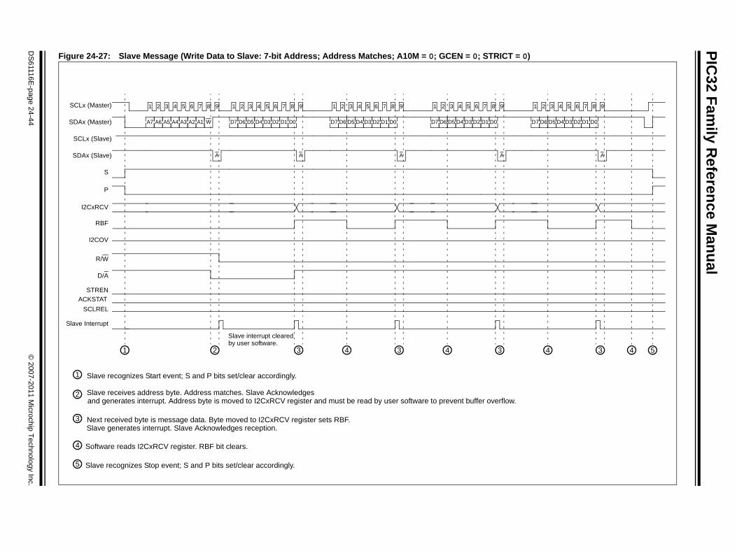
PIC32 Fam
ily Reference M
anual
DS
61116E-page 24-44
© 2007-2011 M
icrochip Technology Inc.
ICT = 0)
3 3 5
9
A
D7 D6 D5 D4 D3 D2 D1
1 2 3 4 5 6 7 8 9
A
4 4
rflow.
D0
Figure 24-27: Slave Message (Write Data to Slave: 7-bit Address; Address Matches; A10M = 0; GCEN = 0; STR
1 Slave recognizes Start event; S and P bits set/clear accordingly.
SCLx (Master)
SDAx (Master)
SCLx (Slave)
SDAx (Slave)
I2CxRCV
RBF
Slave Interrupt
STREN
1 2 3 4 5 6 7 8
A2 A1
9
A
D7 D6 D5 D4 D3 D2 D1
1 2 3 4 5 6 7 8 9
1 32
A
4 3
2 Slave receives address byte. Address matches. Slave Acknowledges
3 Next received byte is message data. Byte moved to I2CxRCV register sets RBF.
4 Software reads I2CxRCV register. RBF bit clears.
5 Slave recognizes Stop event; S and P bits set/clear accordingly.
Slave generates interrupt. Slave Acknowledges reception.
A7 A6 A5 A4 A3
S
P
I2COV
R/W
D/A
D7 D6 D5 D4 D3 D2 D1
1 2 3 4 5 6 7 8 9
A
D7 D6 D5 D4 D3 D2 D1
1 2 3 4 5 6 7 8
SCLREL
4
and generates interrupt. Address byte is moved to I2CxRCV register and must be read by user software to prevent buffer ove
D0D0D0W
Slave interrupt cleared
ACKSTAT
by user software.
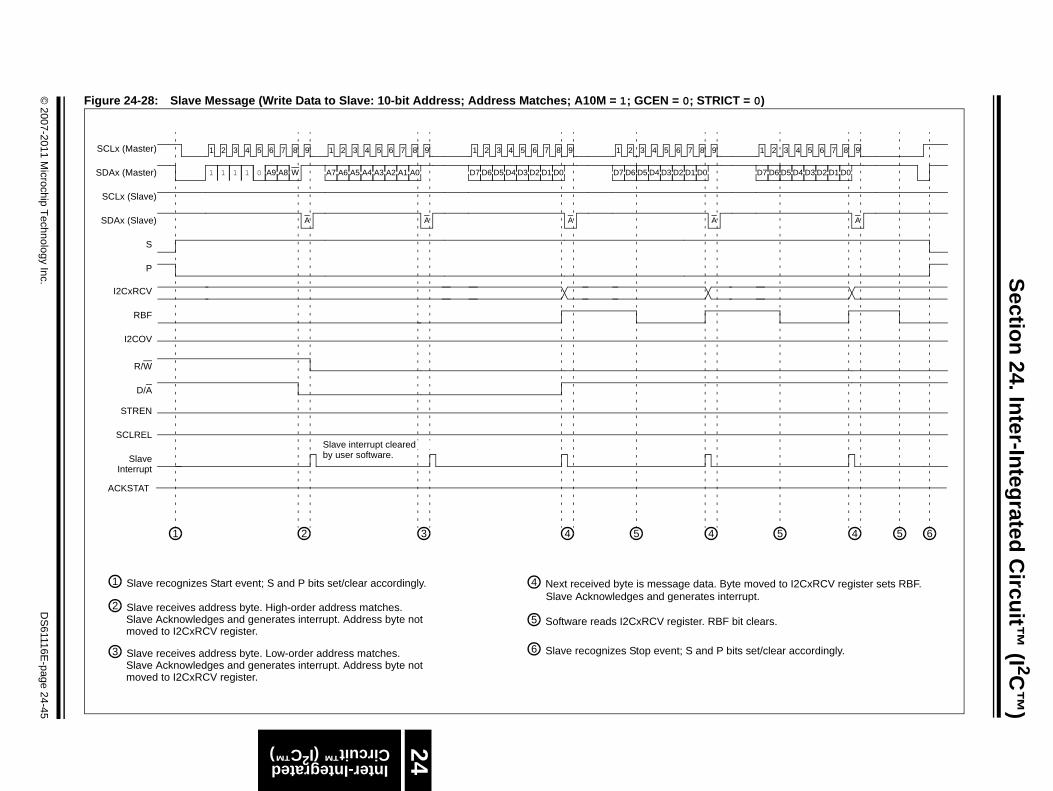
© 2007-2011 M
icrochip Technology Inc.D
S61116E
-page 24-45
Section 24. Inter-Integrated Circuit™
(I 2C™
)
F T = 0)
4 6
te moved to I2CxRCV register sets RBF.
bit clears.
its set/clear accordingly.
rrupt.
D7 D6 D5 D4 D3 D2 D1
1 2 3 4 5 6 7 8 9
A
5 5
D0
Inter-Integrated Circuit™ (I2C™) 24
igure 24-28: Slave Message (Write Data to Slave: 10-bit Address; Address Matches; A10M = 1; GCEN = 0; STRIC
1 Slave recognizes Start event; S and P bits set/clear accordingly.
SCLx (Master)
SDAx (Master)
SCLx (Slave)
SDAx (Slave)
I2CxRCV
RBF
Slave
STREN
1 2 3 4 5 6 7 8
A9 A8
9
A
A7 A6 A5 A4 A3 A2 A1
1 2 3 4 5 6 7 8 9
1 32
A
4 4
2 Slave receives address byte. High-order address matches.
3 Slave receives address byte. Low-order address matches.
4 Next received byte is message data. By
5 Software reads I2CxRCV register. RBF
6 Slave recognizes Stop event; S and P b
Slave Acknowledges and generates interrupt. Address byte not
Slave Acknowledges and generates inte
S
P
I2COV
R/W
D/A
D7 D6 D5 D4 D3 D2 D1
1 2 3 4 5 6 7 8 9
A
D7 D6 D5 D4 D3 D2 D1
1 2 3 4 5 6 7 8 9
A
SCLREL
5
1 1 1 1 0
Slave Acknowledges and generates interrupt. Address byte not
moved to I2CxRCV register.
moved to I2CxRCV register.
A0 D0W D0
Slave interrupt cleared
ACKSTAT
Interruptby user software.
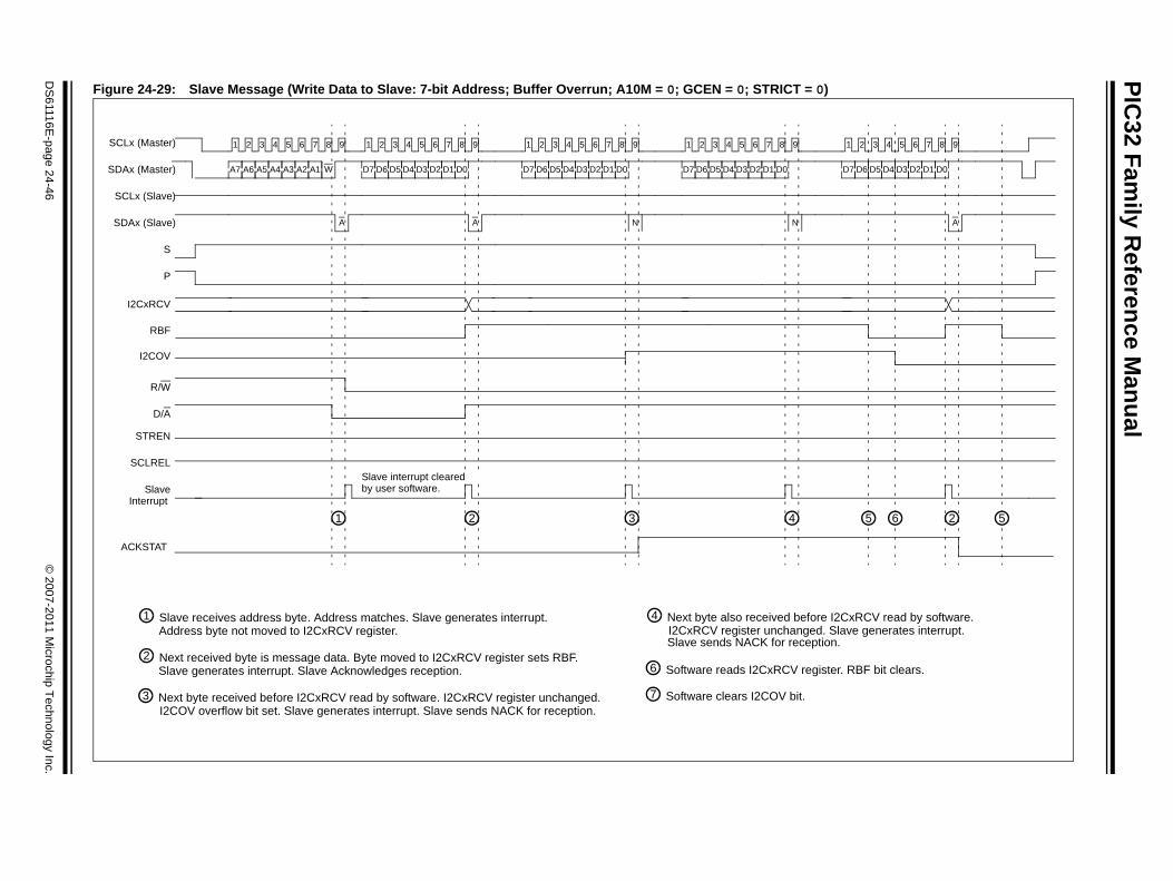
PIC32 Fam
ily Reference M
anual
DS
61116E-page 24-46
© 2007-2011 M
icrochip Technology Inc.
T = 0)
2
register. RBF bit clears.
it.
9
D7 D6 D5 D4 D3 D2 D1
1 2 3 4 5 6 7 8 9
5 5
N A
6
before I2CxRCV read by software.
eception.nged. Slave generates interrupt.
D0
Figure 24-29: Slave Message (Write Data to Slave: 7-bit Address; Buffer Overrun; A10M = 0; GCEN = 0; STRIC
SCLx (Master)
SDAx (Master)
SCLx (Slave)
SDAx (Slave)
I2CxRCV
RBF
Slave
STREN
1 2 3 4 5 6 7 8
A2 A1
9
A
D7 D6 D5 D4 D3 D2 D1
1 2 3 4 5 6 7 8 9
21
A
3 4
1 Slave receives address byte. Address matches. Slave generates interrupt.
2 Next received byte is message data. Byte moved to I2CxRCV register sets RBF.6 Software reads I2CxRCV
7 Software clears I2COV b
Address byte not moved to I2CxRCV register.
Slave generates interrupt. Slave Acknowledges reception.
A7 A6 A5 A4 A3
S
P
I2COV
R/W
D/A
D7 D6 D5 D4 D3 D2 D1
1 2 3 4 5 6 7 8 9
N
D7 D6 D5 D4 D3 D2 D1
1 2 3 4 5 6 7 8
SCLREL
3 Next byte received before I2CxRCV read by software. I2CxRCV register unchanged.I2COV overflow bit set. Slave generates interrupt. Slave sends NACK for reception.
4 Next byte also received
Slave sends NACK for rI2CxRCV register uncha
D0 D0W D0
Slave interrupt cleared
ACKSTAT
Interrupt by user software.

© 2007-2011 M
icrochip Technology Inc.D
S61116E
-page 24-47
Section 24. Inter-Integrated Circuit™
(I 2C™
)
F STRICT = 0)
8 3
clock.
e RBF = 0 at this time.
D7 D6 D5 D3 D2 D1
1 2 3 4 5 6 7 8 9
A
9 5
D4
a clock hold. Module must detect SCLx low
a clock hold.
D0
Inter-Integrated Circuit™ (I2C™) 24
igure 24-30: Slave Message (Write Data to Slave: 7-bit Address; Clock Stretching Enabled; A10M = 0; GCEN = 0;
1 Software sets the STREN bit to enable clock stretching.
SCLx (Master)
SDAx (Master)
SCLx (Slave)
SDAx (Slave)
I2CxTRN
TBF
I2CRCV
RBF
Slave
STREN
1 2 3 4 5 6 7 8
A2 A1
9
A
D7 D6 D5 D4 D3 D2 D1
1 2 3 4 5 6 7 8 9
32
A
5 3
2 Slave receives address byte.
3 Next received byte is message data. Byte moved to I2CxRCV register sets RBF.
6 Software sets SCLREL bit to release
7 Slave does not clear SCLREL becaus
A7 A6 A5 A4 A3
S
P
I2COV
R/W
D/A
D7 D6 D5 D4 D3 D2 D1
1 2 3 4 5 6 7 8 9
A
SCLREL
54 6 71
4 Because RBF = 1 at ninth clock, automatic clock stretch begins. Slave clears SCLREL bit. Slave pulls SCLx line low to stretch clock.
5 Software reads I2CxRCV register. RBF bit clears.
8 Software may clear SCLREL to cause
9 Software may set SCLREL to release
before asserting SCLx low.
D0W D0
ACKSTAT
Interrupt
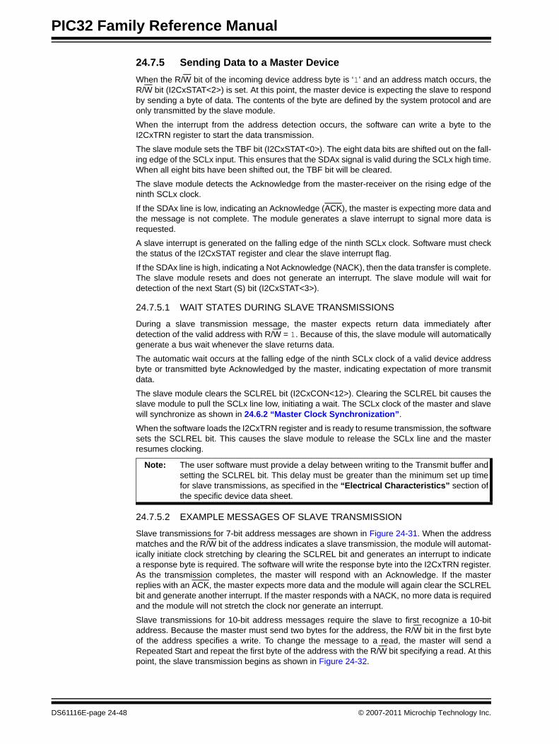
PIC32 Family Reference Manual
24.7.5 Sending Data to a Master DeviceWhen the R/W bit of the incoming device address byte is ‘1’ and an address match occurs, the R/W bit (I2CxSTAT<2>) is set. At this point, the master device is expecting the slave to respond by sending a byte of data. The contents of the byte are defined by the system protocol and are only transmitted by the slave module.
When the interrupt from the address detection occurs, the software can write a byte to the I2CxTRN register to start the data transmission.
The slave module sets the TBF bit (I2CxSTAT<0>). The eight data bits are shifted out on the fall-ing edge of the SCLx input. This ensures that the SDAx signal is valid during the SCLx high time. When all eight bits have been shifted out, the TBF bit will be cleared.
The slave module detects the Acknowledge from the master-receiver on the rising edge of the ninth SCLx clock.
If the SDAx line is low, indicating an Acknowledge (ACK), the master is expecting more data and the message is not complete. The module generates a slave interrupt to signal more data is requested.
A slave interrupt is generated on the falling edge of the ninth SCLx clock. Software must check the status of the I2CxSTAT register and clear the slave interrupt flag.
If the SDAx line is high, indicating a Not Acknowledge (NACK), then the data transfer is complete. The slave module resets and does not generate an interrupt. The slave module will wait for detection of the next Start (S) bit (I2CxSTAT<3>).
24.7.5.1 WAIT STATES DURING SLAVE TRANSMISSIONS
During a slave transmission message, the master expects return data immediately after detection of the valid address with R/W = 1. Because of this, the slave module will automatically generate a bus wait whenever the slave returns data.
The automatic wait occurs at the falling edge of the ninth SCLx clock of a valid device address byte or transmitted byte Acknowledged by the master, indicating expectation of more transmit data.
The slave module clears the SCLREL bit (I2CxCON<12>). Clearing the SCLREL bit causes the slave module to pull the SCLx line low, initiating a wait. The SCLx clock of the master and slave will synchronize as shown in 24.6.2 “Master Clock Synchronization”.
When the software loads the I2CxTRN register and is ready to resume transmission, the software sets the SCLREL bit. This causes the slave module to release the SCLx line and the master resumes clocking.
24.7.5.2 EXAMPLE MESSAGES OF SLAVE TRANSMISSION
Slave transmissions for 7-bit address messages are shown in Figure 24-31. When the address matches and the R/W bit of the address indicates a slave transmission, the module will automat-ically initiate clock stretching by clearing the SCLREL bit and generates an interrupt to indicate a response byte is required. The software will write the response byte into the I2CxTRN register. As the transmission completes, the master will respond with an Acknowledge. If the master replies with an ACK, the master expects more data and the module will again clear the SCLREL bit and generate another interrupt. If the master responds with a NACK, no more data is required and the module will not stretch the clock nor generate an interrupt.
Slave transmissions for 10-bit address messages require the slave to first recognize a 10-bit address. Because the master must send two bytes for the address, the R/W bit in the first byte of the address specifies a write. To change the message to a read, the master will send a Repeated Start and repeat the first byte of the address with the R/W bit specifying a read. At this point, the slave transmission begins as shown in Figure 24-32.
Note: The user software must provide a delay between writing to the Transmit buffer and setting the SCLREL bit. This delay must be greater than the minimum set up time for slave transmissions, as specified in the “Electrical Characteristics” section of the specific device data sheet.
DS61116E-page 24-48 © 2007-2011 Microchip Technology Inc.
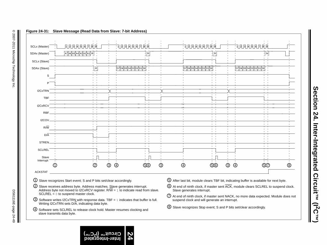
© 2007-2011 M
icrochip Technology Inc.D
S61116E
-page 24-49
Section 24. Inter-Integrated Circuit™
(I 2C™
)
F
8
CK, module clears SCLREL to suspend clock.
bits set/clear accordingly.
4
D7 D6 D5 D4 D3 D2 D1
1 2 3 4 5 6 7 8 9
N
5 7
dicating buffer is available for next byte.
ACK, no more data expected. Module does not terrupt.
D0
Inter-Integrated Circuit™ (I2C™) 24
igure 24-31: Slave Message (Read Data from Slave: 7-bit Address)
1 Slave recognizes Start event; S and P bits set/clear accordingly.
SCLx (Master)
SDAx (Master)
SCLx (Slave)
SDAx (Slave)
I2CxTRN
TBF
I2CxRCV
RBF
Slave
STREN
1 2 3 4 5 6 7 8
A2 A1
9
A D7 D6 D5 D4 D3 D2 D1
1 2 3 4 5 6 7 8 9
R
1 42
A
5 3 5 3
2 Slave receives address byte. Address matches. Slave generates interrupt.
3 Software writes I2CxTRN with response data. TBF = 1 indicates that buffer is full.
6 At end of ninth clock, if master sent A
8 Slave recognizes Stop event; S and P
Address byte not moved to I2CxRCV register. R/W = 1 to indicate read from slave.
Writing I2CxTRN sets D/A, indicating data byte.
A7 A6 A5 A4 A3
S
P
I2COV
R/W
D/A
SCLREL
4
D7 D6 D5 D4 D3 D2 D1
1 2 3 4 5 6 7 8 9
A
3 6 6
SCLREL = 0 to suspend master clock.
4 Software sets SCLREL to release clock hold. Master resumes clocking andslave transmits data byte.
5 After last bit, module clears TBF bit, in
Slave generates interrupt.
7 At end of ninth clock, if master sent Nsuspend clock and will generate an in
D0 D0
ACKSTAT
Interrupt
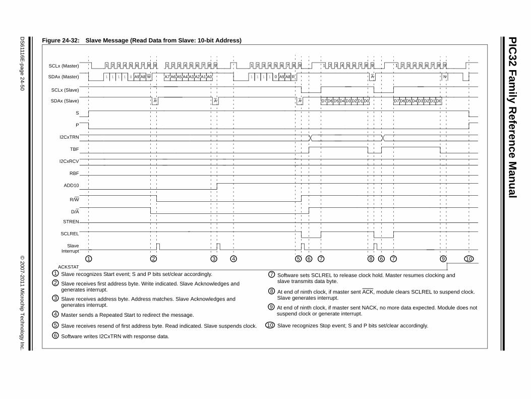
PIC32 Fam
ily Reference M
anual
DS
61116E-page 24-50
© 2007-2011 M
icrochip Technology Inc.
8
t ACK, module clears SCLREL to suspend clock.
d P bits set/clear accordingly.
6
D7 D6 D5 D4 D3 D2 D1
1 2 3 4 5 6 7 8 9
N
97
clock hold. Master resumes clocking and
t NACK, no more data expected. Module does not t.
1
7 8 9
A
10
D0D0
Figure 24-32: Slave Message (Read Data from Slave: 10-bit Address)
1 Slave recognizes Start event; S and P bits set/clear accordingly.
SCLx (Master)
SDAx (Master)
SCLx (Slave)
SDAx (Slave)
I2CxTRN
TBF
I2CxRCV
RBF
Slave
STREN
1 2 3 4 5 6 7 8 9
A
1 42 7
2 Slave receives first address byte. Write indicated. Slave Acknowledges and
6 Software writes I2CxTRN with response data.
8 At end of ninth clock, if master sen
Slave recognizes Stop event; S an
S
P
ADD10
R/W
D/A
SCLREL
53 6
7 Software sets SCLREL to release slave transmits data byte.
Slave generates interrupt.
9 At end of ninth clock, if master sensuspend clock or generate interrup
A7 A6 A5 A4 A3 A2 A1
1 2 3 4 5 6 7 8 9
A
A9 A81 1 1 1 0
1 2 3 4 5 6 7 8 9
A
A9 A81 1 1 1 0
D7 D6 D5 D4 D3 D2 D
1 2 3 4 5 6
3 Slave receives address byte. Address matches. Slave Acknowledges and
10
4 Master sends a Repeated Start to redirect the message.
5 Slave receives resend of first address byte. Read indicated. Slave suspends clock.
R
generates interrupt.
generates interrupt.
A0W
ACKSTAT
Interrupt
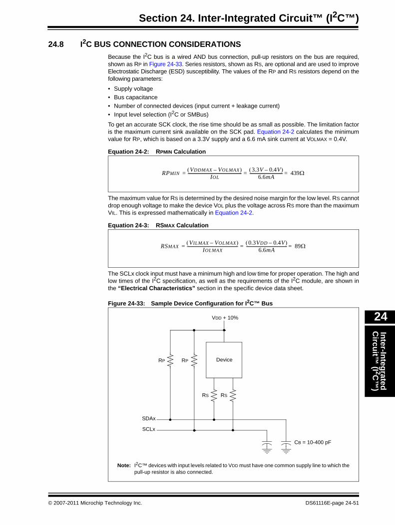
Section 24. Inter-Integrated Circuit™ (I2C™)Inter-Integrated C
ircuit™ (I 2C
™)
24
24.8 I2C BUS CONNECTION CONSIDERATIONSBecause the I2C bus is a wired AND bus connection, pull-up resistors on the bus are required, shown as RP in Figure 24-33. Series resistors, shown as RS, are optional and are used to improve Electrostatic Discharge (ESD) susceptibility. The values of the RP and RS resistors depend on the following parameters:
• Supply voltage• Bus capacitance• Number of connected devices (input current + leakage current)• Input level selection (I2C or SMBus)
To get an accurate SCK clock, the rise time should be as small as possible. The limitation factor is the maximum current sink available on the SCK pad. Equation 24-2 calculates the minimum value for RP, which is based on a 3.3V supply and a 6.6 mA sink current at VOLMAX = 0.4V.
Equation 24-2: RPMIN Calculation
The maximum value for RS is determined by the desired noise margin for the low level. RS cannot drop enough voltage to make the device VOL plus the voltage across RS more than the maximum VIL. This is expressed mathematically in Equation 24-2.
Equation 24-3: RSMAX Calculation
The SCLx clock input must have a minimum high and low time for proper operation. The high and low times of the I2C specification, as well as the requirements of the I2C module, are shown in the “Electrical Characteristics” section in the specific device data sheet.
Figure 24-33: Sample Device Configuration for I2C™ Bus
RPMINVDDMAX VOLMAX–( )
IOL------------------------------------------------------ 3.3V 0.4V–( )
6.6mA--------------------------------- 439Ω===
RSMAXVILMAX VOLMAX–( )
IOLMAX--------------------------------------------------- 0.3VDD 0.4V–( )
6.6mA----------------------------------------- 89Ω===
RPRP
VDD + 10%
SDAx
SCLx
Device
CB = 10-400 pF
RSRS
Note: I2C™ devices with input levels related to VDD must have one common supply line to which the pull-up resistor is also connected.
© 2007-2011 Microchip Technology Inc. DS61116E-page 24-51
PIC32 Family Reference Manual
24.8.1 Integrated Signal Conditioning and Slope ControlThe SCLx and SDAx pins have an input glitch filter. The I2C bus requires this filter in both the 100 kHz and 400 kHz systems.
When operating on a 400 kHz bus, the I2C specification requires a slew rate control of the device pin output. This slew rate control is integrated into the device. If the DISSLW bit (I2CxCON<9>) is cleared, the slew rate control is active. For other bus speeds, the I2C specification does not require slew rate control and the DISSLW bit should be set.
Some system implementations of I2C busses require different input levels for VILMAX and VIHMIN. In a normal I2C system, VILMAX is 0.3 VDD; VIHMIN is 0.7 VDD. By contrast, in a System Management Bus (SMBus) system, VILMAX is set at 0.8V, while VIHMIN is set at 2.1V.
The SMEN bit (I2CxCON<8>) controls the input levels. Setting the SMEN bit (= 1) changes the input levels to SMBus specifications.
DS61116E-page 24-52 © 2007-2011 Microchip Technology Inc.
Section 24. Inter-Integrated Circuit™ (I2C™)Inter-Integrated C
ircuit™ (I 2C
™)
24
24.9 I2C OPERATION IN POWER-SAVING MODESPIC32 devices have two power-saving modes:
• Idle
When the device is in Idle mode, the core and selected peripherals are shut down.
• Sleep
When the device is in Sleep mode, the entire device is shut down.
24.9.1 Sleep in Master Mode OperationWhen the device enters Sleep mode, all clock sources to the module are shut down. The BRG stops because the clocks stop. It may have to be reset to prevent partial clock detection.
If Sleep occurs in the middle of a transmission, and the master state machine is partially into a transmission as the clocks stop, the Master mode transmission is aborted.
There is no automatic way to prevent entry into Sleep mode if a transmission or reception is pending. The user software must synchronize Sleep mode entry with I2C operation to avoid aborted transmissions.
Register contents are not affected by going into Sleep mode or coming out of Sleep mode.
24.9.2 Sleep in Slave Mode OperationThe I2C module can still function in Slave mode operation while the device is in Sleep mode.
When operating in Slave mode and the device is put into Sleep mode, the master-generated clock will run the slave state machine. This feature provides an interrupt to the device upon reception of the address match in order to wake-up the device.
Register contents are not affected by going into Sleep mode or coming out of Sleep mode.
It is an error condition to set Sleep mode in the middle of a slave data transmit operation, as indeterminate results may occur.
24.9.3 Idle ModeWhen the device enters Idle mode, all PBCLK clock sources remain functional. If the module intends to power down, it disables its own clocks.
For the I2C module, the I2CxSIDL bit (I2CxCON<13>) selects whether the module will stop on Idle mode or continue on Idle. If I2CxSIDL = 0, the module will continue operation in Idle mode. If I2CxSIDL = 1, the module will stop on Idle.
The I2C module will perform the same procedures for stop on Idle mode as for Sleep mode. The module state machines must be reset.
Note: As per the slave I2C behavior, a slave interrupt is generated only on an address match. Therefore, when an I2C slave is in Sleep mode and it receives a message from the master, the clock required to match the received address is derived from the master. Only on an address match will the interrupt be generated and the device can wake up, provided the interrupt has been enabled and an ISR has been defined.
© 2007-2011 Microchip Technology Inc. DS61116E-page 24-53
PIC32 Family Reference Manual
24.10 EFFECTS OF A RESETA Reset (POR, WDT, etc.) disables the I2C module and terminates any active or pending message activity. See the I2CxCON and I2CxSTAT register definitions for the Reset conditions of those registers.
24.11 PIN CONFIGURATION IN I2C MODEIn I2C mode, the SCLx pin is the clock and the SDAx pin is data. The module will override the data direction bits (TRISx bits) for these pins. The pins that are used for I2C modes are configured as open drain. Table 24-6 lists the pin usage in different modes.
Table 24-6: Required I/O Pin Resources
Note: Idle refers to the CPU power-saving mode. The word idle in all lowercase letters refers to the time when the I2C module is not transferring data on the bus.
I/O Pin Name Master Mode Slave Mode
SDAx Yes YesSCLx Yes Yes
DS61116E-page 24-54 © 2007-2011 Microchip Technology Inc.
Section 24. Inter-Integrated Circuit™ (I2C™)Inter-Integrated C
ircuit™ (I 2C
™)
24
24.12 RELATED APPLICATION NOTESThis section lists application notes that are related to this section of the manual. These application notes may not be written specifically for the PIC32 device family, but the concepts are pertinent and could be used with modification and possible limitations. The current application notes related to the Inter-Integrated Circuit™ (I2C™) module include the following:
Title Application Note #Use of the SSP Module in the I 2C™ Multi-Master Environment AN578
Using the PIC® Microcontroller SSP for Slave I2C™ Communication AN734
Using the PIC® Microcontroller MSSP Module for Master I2C™ Communications AN735
An I2C™ Network Protocol for Environmental Monitoring AN736
Note: Please visit the Microchip web site (www.microchip.com) for additional application notes and code examples for the PIC32 family of devices.
© 2007-2011 Microchip Technology Inc. DS61116E-page 24-55
PIC32 Family Reference Manual
24.13 REVISION HISTORYRevision A (October 2007)This is the initial released version of this document.
Revision B (October 2007)Updated document to remove Confidential status.
Revision C (April 2008)Revised status to Preliminary; Revised U-0 to r-x.
Revision D (July 2008)Revised Figure 24-1; Section 24.2 (I2CxMIF); Register 24-1, bits 13 and 14; Revised Register 24-26-24-29; Revised Table 24-1, I2CxCON; Change Reserved bits from “Maintain as” to “Write”; Added Note to ON bit (I2CXCON Register); Deleted Section 24.12 (Electrical Characteristics).
Revision E (October 2011)This revision includes the following updates:
• Updated the I2C Block Diagram (see Figure 24-1)• I2C Special Function Register Summary (see Table 24-1):
- Removed the Clear, Set, and Invert registers and their references- Updated the name for bits <7:0> in the I2CxTRN and I2CxRCV registers to
I2CxTXDATA and I2CxRXDATA, respectively- Removed the interrupt registers (IFS0, IEC0, IPC6, and IPC8) and their references- Added Notes 3, 4, and 5, which describe the Clear, Set, and Invert registers
• Changed all occurrences of r-x to U-0 in all registers• Updated the name for bits <7:0> in the I2CxTRN and I2CxRCV registers to I2CxTXDATA
and I2CxRXDATA, respectively (see Register 24-6 and Register 24-7)• Updated the Baud Rate Generator Reload Value Calculation (see Equation 24-1)• Updated all I2CxBRG values and added the PTG column and Note 1 to I2C Clock Rate with
BRG (see Table 24-2)• Added a note (or notes) to the following sections:
- 24.5.2.1 “Sending a 7-bit Address to the Slave”- 24.5.2.2 “Sending a 10-bit Address to the Slave”- 24.7.5.1 “Wait States During Slave Transmissions”- 24.9.2 “Sleep in Slave Mode Operation”
• Updated Master Message (7-bit Address: Transmission and Reception) (see Figure 24-16)• Removed 24.12 “Design Tips”• The Preliminary document status was removed• Additional updates to text and formatting were incorporated throughout the document
DS61116E-page 24-56 © 2007-2011 Microchip Technology Inc.
Note the following details of the code protection feature on Microchip devices:• Microchip products meet the specification contained in their particular Microchip Data Sheet.
• Microchip believes that its family of products is one of the most secure families of its kind on the market today, when used in the intended manner and under normal conditions.
• There are dishonest and possibly illegal methods used to breach the code protection feature. All of these methods, to our knowledge, require using the Microchip products in a manner outside the operating specifications contained in Microchip’s Data Sheets. Most likely, the person doing so is engaged in theft of intellectual property.
• Microchip is willing to work with the customer who is concerned about the integrity of their code.
• Neither Microchip nor any other semiconductor manufacturer can guarantee the security of their code. Code protection does not mean that we are guaranteeing the product as “unbreakable.”
Code protection is constantly evolving. We at Microchip are committed to continuously improving the code protection features of our products. Attempts to break Microchip’s code protection feature may be a violation of the Digital Millennium Copyright Act. If such acts allow unauthorized access to your software or other copyrighted work, you may have a right to sue for relief under that Act.
Information contained in this publication regarding device applications and the like is provided only for your convenience and may be superseded by updates. It is your responsibility to ensure that your application meets with your specifications. MICROCHIP MAKES NO REPRESENTATIONS OR WARRANTIES OF ANY KIND WHETHER EXPRESS OR IMPLIED, WRITTEN OR ORAL, STATUTORY OR OTHERWISE, RELATED TO THE INFORMATION, INCLUDING BUT NOT LIMITED TO ITS CONDITION, QUALITY, PERFORMANCE, MERCHANTABILITY OR FITNESS FOR PURPOSE. Microchip disclaims all liability arising from this information and its use. Use of Microchip devices in life support and/or safety applications is entirely at the buyer’s risk, and the buyer agrees to defend, indemnify and hold harmless Microchip from any and all damages, claims, suits, or expenses resulting from such use. No licenses are conveyed, implicitly or otherwise, under any Microchip intellectual property rights.
© 2007-2011 Microchip Technology Inc.
Trademarks
The Microchip name and logo, the Microchip logo, dsPIC, KEELOQ, KEELOQ logo, MPLAB, PIC, PICmicro, PICSTART, PIC32 logo, rfPIC and UNI/O are registered trademarks of Microchip Technology Incorporated in the U.S.A. and other countries.
FilterLab, Hampshire, HI-TECH C, Linear Active Thermistor, MXDEV, MXLAB, SEEVAL and The Embedded Control Solutions Company are registered trademarks of Microchip Technology Incorporated in the U.S.A.
Analog-for-the-Digital Age, Application Maestro, chipKIT, chipKIT logo, CodeGuard, dsPICDEM, dsPICDEM.net, dsPICworks, dsSPEAK, ECAN, ECONOMONITOR, FanSense, HI-TIDE, In-Circuit Serial Programming, ICSP, Mindi, MiWi, MPASM, MPLAB Certified logo, MPLIB, MPLINK, mTouch, Omniscient Code Generation, PICC, PICC-18, PICDEM, PICDEM.net, PICkit, PICtail, REAL ICE, rfLAB, Select Mode, Total Endurance, TSHARC, UniWinDriver, WiperLock and ZENA are trademarks of Microchip Technology Incorporated in the U.S.A. and other countries.
SQTP is a service mark of Microchip Technology Incorporated in the U.S.A.
All other trademarks mentioned herein are property of their respective companies.
© 2007-2011, Microchip Technology Incorporated, Printed in the U.S.A., All Rights Reserved.
Printed on recycled paper.
ISBN: 978-1-61341-744-7
DS61116E-page 24 -57
Microchip received ISO/TS-16949:2009 certification for its worldwide headquarters, design and wafer fabrication facilities in Chandler and Tempe, Arizona; Gresham, Oregon and design centers in California and India. The Company’s quality system processes and procedures are for its PIC® MCUs and dsPIC® DSCs, KEELOQ® code hopping devices, Serial EEPROMs, microperipherals, nonvolatile memory and analog products. In addition, Microchip’s quality system for the design and manufacture of development systems is ISO 9001:2000 certified.
DS61116E-page 24 -58 © 2007-2011 Microchip Technology Inc.
AMERICASCorporate Office2355 West Chandler Blvd.Chandler, AZ 85224-6199Tel: 480-792-7200 Fax: 480-792-7277Technical Support: http://www.microchip.com/supportWeb Address: www.microchip.comAtlantaDuluth, GA Tel: 678-957-9614 Fax: 678-957-1455BostonWestborough, MA Tel: 774-760-0087 Fax: 774-760-0088ChicagoItasca, IL Tel: 630-285-0071 Fax: 630-285-0075ClevelandIndependence, OH Tel: 216-447-0464 Fax: 216-447-0643DallasAddison, TX Tel: 972-818-7423 Fax: 972-818-2924DetroitFarmington Hills, MI Tel: 248-538-2250Fax: 248-538-2260IndianapolisNoblesville, IN Tel: 317-773-8323Fax: 317-773-5453Los AngelesMission Viejo, CA Tel: 949-462-9523 Fax: 949-462-9608Santa ClaraSanta Clara, CA Tel: 408-961-6444Fax: 408-961-6445TorontoMississauga, Ontario, CanadaTel: 905-673-0699 Fax: 905-673-6509
ASIA/PACIFICAsia Pacific OfficeSuites 3707-14, 37th FloorTower 6, The GatewayHarbour City, KowloonHong KongTel: 852-2401-1200Fax: 852-2401-3431Australia - SydneyTel: 61-2-9868-6733Fax: 61-2-9868-6755China - BeijingTel: 86-10-8569-7000 Fax: 86-10-8528-2104China - ChengduTel: 86-28-8665-5511Fax: 86-28-8665-7889China - ChongqingTel: 86-23-8980-9588Fax: 86-23-8980-9500China - HangzhouTel: 86-571-2819-3187 Fax: 86-571-2819-3189China - Hong Kong SARTel: 852-2401-1200 Fax: 852-2401-3431China - NanjingTel: 86-25-8473-2460Fax: 86-25-8473-2470China - QingdaoTel: 86-532-8502-7355Fax: 86-532-8502-7205China - ShanghaiTel: 86-21-5407-5533 Fax: 86-21-5407-5066China - ShenyangTel: 86-24-2334-2829Fax: 86-24-2334-2393China - ShenzhenTel: 86-755-8203-2660 Fax: 86-755-8203-1760China - WuhanTel: 86-27-5980-5300Fax: 86-27-5980-5118China - XianTel: 86-29-8833-7252Fax: 86-29-8833-7256China - XiamenTel: 86-592-2388138 Fax: 86-592-2388130China - ZhuhaiTel: 86-756-3210040 Fax: 86-756-3210049
ASIA/PACIFICIndia - BangaloreTel: 91-80-3090-4444 Fax: 91-80-3090-4123India - New DelhiTel: 91-11-4160-8631Fax: 91-11-4160-8632India - PuneTel: 91-20-2566-1512Fax: 91-20-2566-1513Japan - YokohamaTel: 81-45-471- 6166 Fax: 81-45-471-6122Korea - DaeguTel: 82-53-744-4301Fax: 82-53-744-4302Korea - SeoulTel: 82-2-554-7200Fax: 82-2-558-5932 or 82-2-558-5934Malaysia - Kuala LumpurTel: 60-3-6201-9857Fax: 60-3-6201-9859Malaysia - PenangTel: 60-4-227-8870Fax: 60-4-227-4068Philippines - ManilaTel: 63-2-634-9065Fax: 63-2-634-9069SingaporeTel: 65-6334-8870Fax: 65-6334-8850Taiwan - Hsin ChuTel: 886-3-5778-366Fax: 886-3-5770-955Taiwan - KaohsiungTel: 886-7-536-4818Fax: 886-7-330-9305Taiwan - TaipeiTel: 886-2-2500-6610 Fax: 886-2-2508-0102Thailand - BangkokTel: 66-2-694-1351Fax: 66-2-694-1350
EUROPEAustria - WelsTel: 43-7242-2244-39Fax: 43-7242-2244-393Denmark - CopenhagenTel: 45-4450-2828 Fax: 45-4485-2829France - ParisTel: 33-1-69-53-63-20 Fax: 33-1-69-30-90-79Germany - MunichTel: 49-89-627-144-0 Fax: 49-89-627-144-44Italy - Milan Tel: 39-0331-742611 Fax: 39-0331-466781Netherlands - DrunenTel: 31-416-690399 Fax: 31-416-690340Spain - MadridTel: 34-91-708-08-90Fax: 34-91-708-08-91UK - WokinghamTel: 44-118-921-5869Fax: 44-118-921-5820
Worldwide Sales and Service
08/02/11