Embed Size (px)
Citation preview
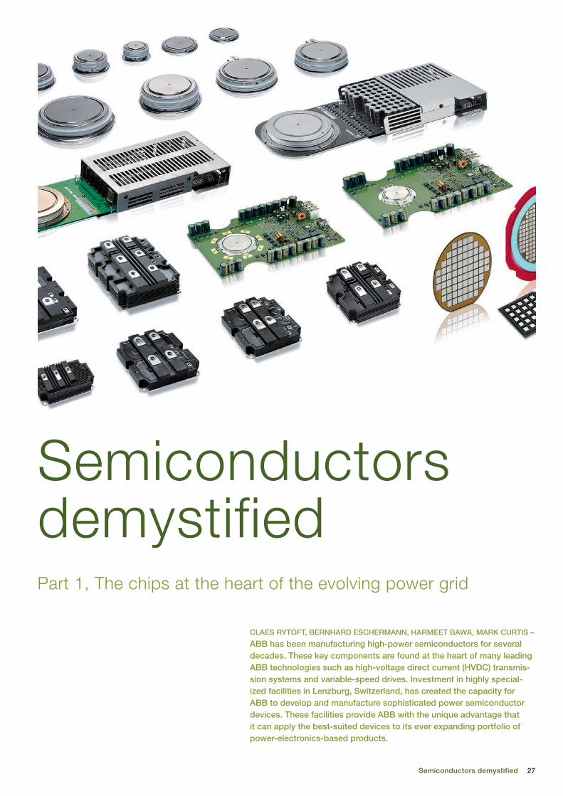
27Semiconductors demystified
CLAES RyToFT, BERnHARD ESCHERMAnn, HARMEET BAWA, MARk CuRTIS –
ABB has been manufacturing high-power semiconductors for several decades. These key components are found at the heart of many leading ABB technologies such as high-voltage direct current (HvDC) transmis-sion systems and variable-speed drives. Investment in highly special-ized facilities in Lenzburg, Switzerland, has created the capacity for ABB to develop and manufacture sophisticated power semiconductor devices. These facilities provide ABB with the unique advantage that it can apply the best-suited devices to its ever expanding portfolio of power-electronics-based products.
Part 1, The chips at the heart of the evolving power grid
Semiconductors demystified
28 ABB review 3|10
P ower electronics deals with the conversion and control of electricity using solid-state switching devices ➔ 1. In re-
cent years advances in power semicon-ductor technology have resulted in an ever expanding array of applications. The adverse effects of global warming, re-sulting from the burning of fossil fuels, have played a major role in driving the in-creased use of power semiconductor technologies aimed at utilizing renewable energy generation and increasing energy efficiency.
Even in the very early days of electricity, transmission efficiency had an impact on the type of electricity that prevailed, ie, direct current (DC) or alternating current (AC). Initially, for historic reasons, electric power systems were predominantly DC circuits. However, the inability to alter DC voltage levels, at that time, limited its use. Power generators were built there-fore to satisfy the load on the circuit (eg, at a voltage level required for lighting or motors). Inefficient transmission at such low voltages meant that these genera-tors had to remain within a short distance of consumers.
The subsequent development of AC gen-erators and transformers provided the much needed technology that would allow power to be stepped up to 110 kV or more, to facilitate efficient long-dis-tance power transmission. This meant
1 Power electronics
Power electronics stems from the discovery of semiconductors and identifies a significant change in technology toward solid-state elec- tronic switches* as a means to modify electricity.
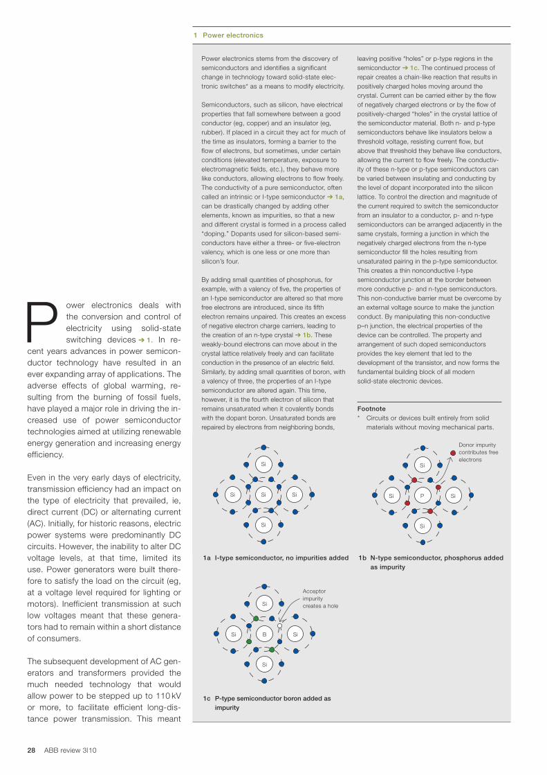
Semiconductors, such as silicon, have electrical properties that fall somewhere between a good conductor (eg, copper) and an insulator (eg, rubber). If placed in a circuit they act for much of the time as insulators, forming a barrier to the flow of electrons, but sometimes, under certain conditions (elevated temperature, exposure to electromagnetic fields, etc.), they behave more like conductors, allowing electrons to flow freely. The conductivity of a pure semiconductor, often called an intrinsic or I-type semiconductor ➔ 1a, can be drastically changed by adding other elements, known as impurities, so that a new and different crystal is formed in a process called “doping.” Dopants used for silicon-based semi - conductors have either a three- or five-electron valency, which is one less or one more than silicon’s four.
By adding small quantities of phosphorus, for example, with a valency of five, the properties of an I-type semiconductor are altered so that more free electrons are introduced, since its fifth electron remains unpaired. This creates an excess of negative electron charge carriers, leading to the creation of an n-type crystal ➔ 1b. These weakly-bound electrons can move about in the crystal lattice relatively freely and can facilitate conduction in the presence of an electric field. Similarly, by adding small quantities of boron, with a valency of three, the properties of an I-type semiconductor are altered again. This time, however, it is the fourth electron of silicon that remains unsaturated when it covalently bonds with the dopant boron. Unsaturated bonds are repaired by electrons from neighboring bonds,
leaving positive “holes” or p-type regions in the semiconductor ➔ 1c. The continued process of repair creates a chain-like reaction that results in positively charged holes moving around the crystal. Current can be carried either by the flow of negatively charged electrons or by the flow of positively-charged “holes” in the crystal lattice of the semiconductor material. Both n- and p-type semiconductors behave like insulators below a threshold voltage, resisting current flow, but above that threshold they behave like conductors, allowing the current to flow freely. The conductiv-ity of these n-type or p-type semiconductors can be varied between insulating and conducting by the level of dopant incorporated into the silicon lattice. To control the direction and magnitude of the current required to switch the semiconductor from an insulator to a conductor, p- and n-type semiconductors can be arranged adjacently in the same crystals, forming a junction in which the negatively charged electrons from the n-type semiconductor fill the holes resulting from unsaturated pairing in the p-type semiconductor. This creates a thin nonconductive I-type semiconductor junction at the border between more conductive p- and n-type semiconductors. This non-conductive barrier must be overcome by an external voltage source to make the junction conduct. By manipulating this non-conductive p–n junction, the electrical properties of the device can be controlled. The property and arrangement of such doped semiconductors provides the key element that led to the development of the transistor, and now forms the fundamental building block of all modern solid-state electronic devices.
Footnote* Circuits or devices built entirely from solid
materials without moving mechanical parts.
1a I-type semiconductor, no impurities added
Si
SiSi Si
Si
1b n-type semiconductor, phosphorus added as impurity
Si
Donor impuritycontributes free electrons
PSi Si
Si
1c P-type semiconductor boron added as impurity
Si
Acceptorimpuritycreates a hole
BSi Si
Si
29Semiconductors demystified
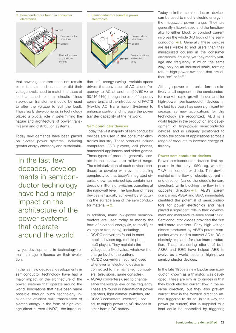
tion of energy-saving variable-speed drives, the conversion of AC at one fre-quency to AC at another (50 / 60 Hz or 50 / 16.6 Hz) through the use of frequency converters, and the introduction of FACTS (Flexible AC Transmission Systems) to enhance control and increase the power transfer capability of the network. Semiconductor devicesToday the vast majority of semiconductor devices are used in the consumer elec-tronics industry. These products include computers, DVD players, cell phones, household appliances and video games. These types of products generally oper-ate in the nanowatt to milliwatt range. The miniaturization of such devices con-tinues to develop with ever increasing complexity so that today’s integrated cir-cuits, known as microchips, contain hun-dreds of millions of switches operating at the nanowatt level. The function of these devices is typically achieved by structur-ing the surface area of the semiconduc-tor material ➔ 2.
In addition, many low-power semicon-ductors are used today to modify the form of electrical energy (ie, to modify its voltage or frequency), including: − DC/DC converters found in most
mobile devices (eg, mobile phone, mp3 player). They maintain the voltage at a fixed value, whatever the charge level of the battery.
− AC/DC converters (rectifiers) used whenever an electronic device is connected to the mains (eg, comput-ers, televisions, game consoles).
− AC/AC converters used to change either the voltage level or the frequency. These are found in international power adapters, light dimmer switches, etc.
− DC/AC converters (inverters) used, eg, to supply power to AC devices in a car from a DC battery.
that power generators need not remain close to their end users, nor did their voltage levels need to match the class of load attached to their circuits (since step-down transformers could be used to alter the voltage to suit the load). These early developments in technology played a pivotal role in determining the nature and architecture of power trans-mission and distribution systems.
Today new demands have been placed on electric power systems, including greater energy efficiency and sustainabil-
ity, yet developments in technology re-main a major influence on their evolu-tion.
In the last few decades, developments in semiconductor technology have had a major impact on the architecture of the power systems that operate around the world. Innovations that have been made possible through such technology in-clude the efficient bulk transmission of electric energy in the form of high-volt-age direct current (HVDC), the introduc-
2 Semiconductors found in consumer electronics
current
Semiconductorstructures
Device functions at the silicon surface
Silicon
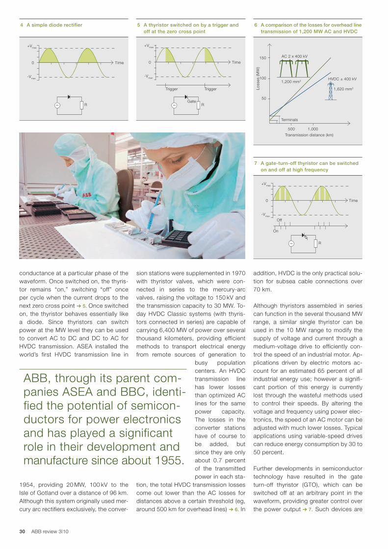
3 Semiconductors found in power electronics
current
Semiconductorstructures
Device functions in the silicon body
Silicon
Today, similar semiconductor devices can be used to modify electric energy in the megawatt power range. They are generally silicon-based and the function-ality to either block or conduct current involves the whole 3-D body of the semi-conductor ➔ 3. Generally these devices are less visible to end users than their miniaturized cousins in the consumer electronics industry, yet they modify volt-age and frequency in much the same way, only on an industrial scale, forming robust high-power switches that are ei-ther “on” or “off.”
Although power electronics form a rela-tively small segment in the semiconduc-tor market, rapid growth in demand for high-power semiconductor devices in the last five years has seen significant in-creases as new applications for this technology are recognized. ABB is a world leader in the production and devel-opment of high-power semiconductor devices and is uniquely positioned to widen the scope of applications across a range of products to increase energy ef-ficiency.
Power semiconductor devicesPower semiconductor devices first ap-peared in the early 1950s eg, with the 7 kW semiconductor diode. This device maintains the flow of electric current in one direction (called the diode’s forward direction), while blocking the flow in the opposite direction ➔ 4. ABB’s parent companies, ASEA and BBC, immediately identified the potential of semiconduc-tors for power electronics and have played a significant role in their develop-ment and manufacture since about 1955. Semiconductor diodes provided the first solid-state rectifiers. Early high-voltage diodes produced by ABB’s parent com-panies were used to convert AC to DC in electrolysis plants for aluminum produc-tion. These pioneering efforts of both ASEA and BBC have helped ABB to evolve as a world leader in high-power semiconductor devices.
In the late 1950s a new bipolar semicon-ductor, known as a thyristor, was devel-oped. These are similar to diodes in that they block electric current flow in the re-verse direction, but they also prevent current flow in the forward direction un-less triggered to do so. In this way, the power (or current) that is supplied to a load could be controlled by triggering
In the last few decades, develop-ments in semicon-ductor technology have had a major impact on the architecture of the power systems that operate around the world.
30 ABB review 3|10
addition, HVDC is the only practical solu-tion for subsea cable connections over 70 km.
Although thyristors assembled in series can function in the several thousand MW range, a similar single thyristor can be used in the 10 MW range to modify the supply of voltage and current through a medium-voltage drive to efficiently con-trol the speed of an industrial motor. Ap-plications driven by electric motors ac-count for an estimated 65 percent of all industrial energy use; however a signifi-cant portion of this energy is currently lost through the wasteful methods used to control their speeds. By altering the voltage and frequency using power elec-tronics, the speed of an AC motor can be adjusted with much lower losses. Typical applications using variable-speed drives can reduce energy consumption by 30 to 50 percent.
Further developments in semiconductor technology have resulted in the gate turn-off thyristor (GTO), which can be switched off at an arbitrary point in the waveform, providing greater control over the power output ➔ 7. Such devices are
sion stations were supplemented in 1970 with thyristor valves, which were con-nected in series to the mercury-arc valves, raising the voltage to 150 kV and the transmission capacity to 30 MW. To-day HVDC Classic systems (with thyris-tors connected in series) are capable of carrying 6,400 MW of power over several thousand kilometers, providing efficient methods to transport electrical energy from remote sources of generation to
busy population centers. An HVDC transmission line has lower losses than optimized AC lines for the same power capacity. The losses in the converter stations have of course to be added, but since they are only about 0.7 percent of the transmitted power in each sta-
tion, the total HVDC transmission losses come out lower than the AC losses for distances above a certain threshold (eg, around 500 km for overhead lines) ➔ 6. In
conductance at a particular phase of the waveform. Once switched on, the thyris-tor remains “on,” switching “off” once per cycle when the current drops to the next zero cross point ➔ 5. Once switched on, the thyristor behaves essentially like a diode. Since thyristors can switch power at the MW level they can be used to convert AC to DC and DC to AC for HVDC transmission. ASEA installed the world’s first HVDC transmission line in
1954, providing 20 MW, 100 kV to the Isle of Gotland over a distance of 96 km. Although this system originally used mer-cury arc rectifiers exclusively, the conver-
4 A simple diode rectifier
+Vmax
-Vmax
0 Time
R~
5 A thyristor switched on by a trigger and off at the zero cross point
+Vmax
-Vmax
0 Time
TriggerTrigger
GateR~
7 A gate-turn-off thyristor can be switched on and off at high frequency
+Vmax
-Vmax
0 Time
Off
On
R~
6 A comparison of the losses for overhead line transmission of 1,200 MW AC and HvDC
Loss
es (M
W)
Transmission distance (km)
Terminals
500 1,000
1,200 mm3
1,620 mm3
AC 2 x 400 kV
HVDC ± 400 kV
150
100
50
ABB, through its parent com-panies ASEA and BBC, identi-fied the potential of semicon-ductors for power electronics and has played a significant role in their development and manufacture since about 1955.
31Semiconductors demystified
Not long after the development of the GTO, an improved type of device known as the integrated gate-commutated thy-ristor (IGCT) was developed. These de-vices, like the GTO, can be switched “on” or “off,” but since their turnoff times are much faster, they can operate at much higher frequencies than GTOs. They are able to cope with high rates of voltage rise and have lower conduction losses. Today there are many thousands of drives worldwide using IGCTs. The IGCT is a single integrated component capable of switching power at high voltage levels and is emerging as a key element in stat-ic var compensators 1 and other compo-nents of the electric grid.
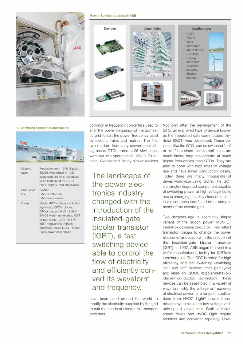
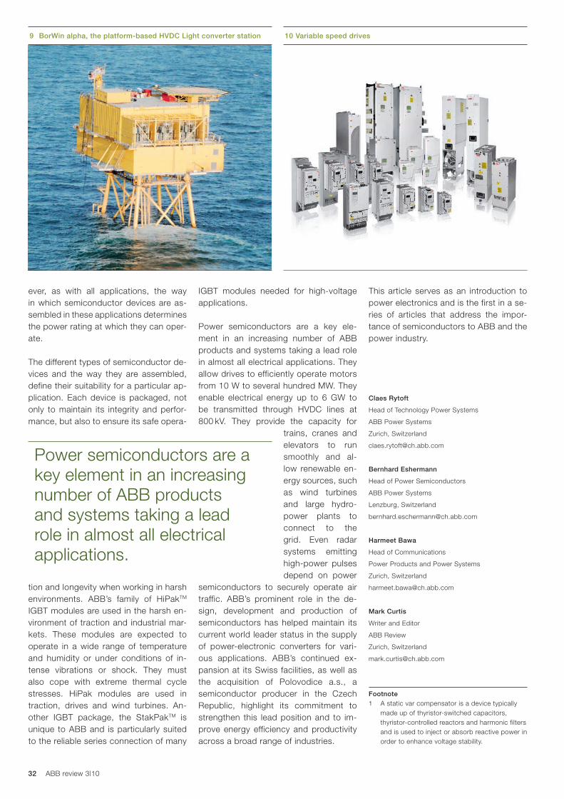
Two decades ago, a seemingly simple variant of the silicon power MOSFET (metal-oxide-semiconductor field-effect transistor) began to change the power electronic landscape with the creation of the insulated-gate bipolar transistor (IGBT). In 1997, ABB began to invest in a wafer manufacturing facility for IGBTs in Lenzburg ➔ 8. The IGBT is noted for high efficiency and fast switching (switching “on” and “off” multiple times per cycle) and relies on BiMOS (bipolar-metal-ox-ide-semiconductor) technology. These devices can be assembled in a variety of ways to modify the voltage or frequency of electrical power for a range of applica-tions from HVDC Light® power trans-mission systems ➔ 9 to low-voltage vari-able-speed drives ➔ 10. Both variable- speed drives and HVDC Light require rectifiers and converter topology. How-
common in frequency converters used to alter the power frequency of the domes-tic grid to suit the power frequency used by electric trains and metros. The first two modern frequency converters mak-ing use of GTOs, rated at 25 MVA each, were put into operation in 1994 in Giubi-asco, Switzerland. Many similar devices
have been used around the world to modify the electricity supplied by the grid to suit the needs of electric rail transport providers.
The landscape of the power elec-tronics industry changed with the introduction of the insulated-gate bipolar transistor (IGBT), a fast switching device able to control the flow of electricity and efficiently con-vert its waveform and frequency.
Power Semiconductors in ABB
Assemblies Applications
– HVDC– FACTS– Wind
converters– Motor drives– Rectifiers– Railway converters– Excitation systems– Electric
mobility
Devices
Factory Production from 1978 (Bipolar), facts BIMOS was added in 1997, expansion ongoing, scheduled to be completed by 2010 / 2011, approx. 500 employees
Production Bipolar line BiMOS wafer-fab BiMOS module-fab
Focus Bipolar (PCTs [phase controlled thyristors], IGCTs, diodes, GTOs), range 1.6 kV - 8.5 kV BiMOS wafer-fab (diodes, IGBT chips), range 1.2 kV - 6.5 kV IGBT module line (HiPaks, StakPaks), range 1.7 kV - 6.5 kV Pulse power assemblies
8 Lenzburg semiconductor facility
32 ABB review 3|10
This article serves as an introduction to power electronics and is the first in a se-ries of articles that address the impor-tance of semiconductors to ABB and the power industry.
Claes Rytoft
Head of Technology Power Systems
ABB Power Systems
Zurich, Switzerland
Bernhard Eshermann
Head of Power Semiconductors
ABB Power Systems
Lenzburg, Switzerland
Harmeet Bawa
Head of Communications
Power Products and Power Systems
Zurich, Switzerland
Mark Curtis
Writer and Editor
ABB Review
Zurich, Switzerland
Footnote1 A static var compensator is a device typically
made up of thyristor-switched capacitors, thyristor-controlled reactors and harmonic filters and is used to inject or absorb reactive power in order to enhance voltage stability.
IGBT modules needed for high-voltage applications.
Power semiconductors are a key ele-ment in an increasing number of ABB products and systems taking a lead role in almost all electrical applications. They allow drives to efficiently operate motors from 10 W to several hundred MW. They enable electrical energy up to 6 GW to be transmitted through HVDC lines at 800 kV. They provide the capacity for
trains, cranes and elevators to run smoothly and al-low renewable en-ergy sources, such as wind turbines and large hydro-power plants to connect to the grid. Even radar systems emitting high-power pulses depend on power
semiconductors to securely operate air traffic. ABB’s prominent role in the de-sign, development and production of semiconductors has helped maintain its current world leader status in the supply of power-electronic converters for vari-ous applications. ABB’s continued ex-pansion at its Swiss facilities, as well as the acquisition of Polovodice a.s., a semiconductor producer in the Czech Republic, highlight its commitment to strengthen this lead position and to im-prove energy efficiency and productivity across a broad range of industries.
ever, as with all applications, the way in which semiconductor devices are as-sembled in these applications determines the power rating at which they can oper-ate.
The different types of semiconductor de-vices and the way they are assembled, define their suitability for a particular ap-plication. Each device is packaged, not only to maintain its integrity and perfor-mance, but also to ensure its safe opera-
tion and longevity when working in harsh environments. ABB’s family of HiPakTM IGBT modules are used in the harsh en-vironment of traction and industrial mar-kets. These modules are expected to operate in a wide range of temperature and humidity or under conditions of in-tense vibrations or shock. They must also cope with extreme thermal cycle stresses. HiPak modules are used in traction, drives and wind turbines. An-other IGBT package, the StakPakTM is unique to ABB and is particularly suited to the reliable series connection of many
9 BorWin alpha, the platform-based HvDC Light converter station 10 variable speed drives
Power semiconductors are a key element in an increasing number of ABB products and systems taking a lead role in almost all electrical applications.