Embed Size (px)
Citation preview
Rhs
Rls
Hi-side current sense
Low-side current senseOPA2376
MCULow side current sensing and output level-shifting difference amplifier
220-V AC Mains-
DC+
DCí
INA170 OPA2376
Voltage follower buffer
High side and low side currentsense voltages are summed together and provided to comparator
Power supply and references (REF2033)
5 V 3.3 V1.65 V
Motor
Vth
Vtl TLC372
Ground FaultTLC372
ADC0
ADC1
INT_N
RectifierInverter
DCbus capacitor
UCC28880 and LM4040
DC+ 2.5 V
DCí
DC+Float_ref
30 V
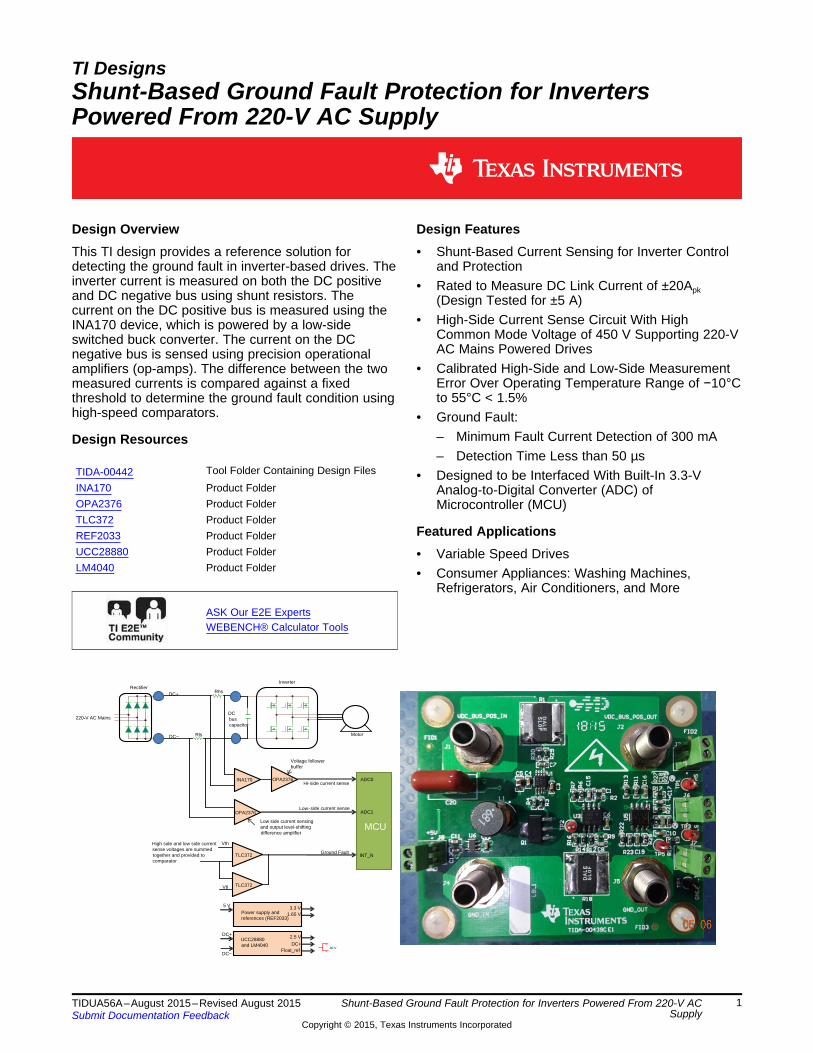
TI DesignsShunt-Based Ground Fault Protection for InvertersPowered From 220-V AC Supply
Design Overview Design FeaturesThis TI design provides a reference solution for • Shunt-Based Current Sensing for Inverter Controldetecting the ground fault in inverter-based drives. The and Protectioninverter current is measured on both the DC positive • Rated to Measure DC Link Current of ±20Apkand DC negative bus using shunt resistors. The (Design Tested for ±5 A)current on the DC positive bus is measured using the
• High-Side Current Sense Circuit With HighINA170 device, which is powered by a low-sideCommon Mode Voltage of 450 V Supporting 220-Vswitched buck converter. The current on the DCAC Mains Powered Drivesnegative bus is sensed using precision operational
• Calibrated High-Side and Low-Side Measurementamplifiers (op-amps). The difference between the twoError Over Operating Temperature Range of −10°Cmeasured currents is compared against a fixedto 55°C < 1.5%threshold to determine the ground fault condition using
high-speed comparators. • Ground Fault:– Minimum Fault Current Detection of 300 mADesign Resources– Detection Time Less than 50 µs
Tool Folder Containing Design FilesTIDA-00442 • Designed to be Interfaced With Built-In 3.3-VINA170 Product Folder Analog-to-Digital Converter (ADC) ofOPA2376 Product Folder Microcontroller (MCU)TLC372 Product Folder
Featured ApplicationsREF2033 Product FolderUCC28880 Product Folder • Variable Speed DrivesLM4040 Product Folder • Consumer Appliances: Washing Machines,
Refrigerators, Air Conditioners, and More
ASK Our E2E ExpertsWEBENCH® Calculator Tools
1TIDUA56A–August 2015–Revised August 2015 Shunt-Based Ground Fault Protection for Inverters Powered From 220-V ACSupplySubmit Documentation Feedback
Copyright © 2015, Texas Instruments Incorporated

Y
L1L2L3
N
Neutral earthedRn
Distribution transformer
DC bus cap
UVW
Earth leakage
Rectifier Inverter
Motor drive
Motor chassis
Earth
Earth
Introduction www.ti.com
An IMPORTANT NOTICE at the end of this TI reference design addresses authorized use, intellectual property matters and otherimportant disclaimers and information.
1 IntroductionGround faults are one of the major causes of drive failures. Early detection of ground faults can avoidmajor drive damage, electrocution of personnel, and fire hazards. This TI design provides a referencesolution to detect ground fault subsequently enabling shutdown of the inverter.
1.1 Ground Fault in DrivesA motor is considered to be a balanced three-phase load, which means that during normal operatingcondition of a drive system, the sum of the three-phase currents drawn from the source must be zero. Dueto faults in the motor winding, faults in the cabling from the drive to the motor, or faults in the drive itself,current can leak into the earth through the chassis of the motor or drive and create ground fault. Currentleak can cause hazardous situations and must be avoided.
Figure 1 shows an example ground fault condition. In a power distribution system the neutral wire isusually connected to the earth at the distribution transformer. In the motor drive system the chassis of thedrive and motor are connected to the earth. Due to deterioration of the motor winding insulation, aresistance path is created between the winding and the chassis of the motor. This resistance path causesan earth leakage current to flow through the chassis into the earth and back into the neutral of thetransformer, as Figure 1 shows.
Figure 1. Ground Fault in Drive
1.2 Causes of Ground FaultThe main causes of ground fault are in the following list:• Faulty wiring: During the installation of a motor drive system, the phase wire can be wrongly
connected to the earth terminal of the motor or there could be a cut in the winding insulation thatcomes into contact with the motor chassis. This type of fault (dead short to earth) can result in highcurrent flow into the earth wire upon starting the drive. This fault can be detected by fuses and circuitbreakers in distribution systems where the transformer star point is connected to earth through lowimpedance. In case of high resistance earthing, where the fault current is limited, the user must utilizeground fault detection devices to detect the leakage current.
• Insulation degradation: The insulation of a motor phase winding to chassis degrades over time dueto heating and aging. Current may start leaking from the phase into the earth through the degradedinsulation.
• Moist environment: Moisture may condense onto the motor windings during the downtime. Thismoisture provides a path to earth and is one of the major causes of ground fault currents. Because ofthis hazard, fault protection is usually provided in moist operating environments such as watertreatment plants, washdown areas of industrial plants, pumping applications, marine applications, andmining applications.
2 Shunt-Based Ground Fault Protection for Inverters Powered From 220-V AC TIDUA56A–August 2015–Revised August 2015Supply Submit Documentation Feedback
Copyright © 2015, Texas Instruments Incorporated

www.ti.com Introduction
• Dust: Dust may provide a high resistance path to earth. Ground fault protection is usually provided toprotect against dust in environments such as cement factories, mines, and gravel quarries.
• Foreign object debris (FOD): During production conductive metal parts such as screws or metalpieces can enter into the motor during metal cutting or grinding. Mechanical vibrations can also causescrews, bolts, nuts, and washers to loosen and fall into the motor, which may lead to contact betweenthe phase winding and chassis.
1.3 Required Use of Ground Fault Protection DevicesMotor drive systems are usually protected by fuses and circuit breakers for overcurrents. The trip levels ofthese protection mechanisms are usually set higher than the maximum current required by the system bya certain margin. Apart from a dead short between the inverter output and earth, even a high resistancepath to earth can cause current leakage into the earth. Earth leakage currents through high resistancepaths are smaller in magnitude and cannot be detected by overcurrent protection mechanisms.
Some of the hazards of ground leakage current are electrocution, arcing (which can pose fire hazards),and damage to the wiring insulation due to the continuous leakage of current through it. Ground currentsalso have an affect on the motor control algorithms if there is a current control loop involved. Groundcurrents are also an early indicator of insulation degradation. A ground fault protection circuit is required toavoid the possible hazards, prevent downtime, and inhibit loss due to a halt in production.
1.4 Ground Fault Sensitivity LevelsGround fault protection devices have different sensitivity levels. A sensitivity level indicates the groundfault current at which the device responds. The sensitivity is expressed as the rated current difference,denoted as IΔn. Based on this rated current difference, the sensitivity levels can be categorized into thefollowing groups:• High sensitivity (HS): 6 to 10 to 30 mA (for direct-contact, life injury, and protection from electrocution)• Medium sensitivity (MS): 100 to 300 to 500 to 1000 mA (for fire protection)• Low sensitivity (LS): 3 to 10 to 30 A (for machine and device protection)
Choose a device with a a high, medium, or low sensitivity based on the application, required protectionlevel, and environment.
3TIDUA56A–August 2015–Revised August 2015 Shunt-Based Ground Fault Protection for Inverters Powered From 220-V ACSupplySubmit Documentation Feedback
Copyright © 2015, Texas Instruments Incorporated

RectifierInverter
DC Bus cap
Motor
TIDA-00442GND Fault Protection
220-V AC Mains
Controller
HMI
DC bus current feedback
DC bus voltage feedback
Speed feedback
PWM control
System Description www.ti.com
2 System DescriptionA typical motor drive system powered from AC mains consists of an AC-DC converter and a DC-ACinverter along with a control circuit. Figure 2 shows the block diagram of the system. The mains supplycan be single phase or three phase, 110-V AC or 220-V AC depending on the drive and the country inwhich the drive is to be used. The drive first converts the AC mains voltage into DC with the help of apower converter. The converter can be an active PFC or may be a simple bridge rectifier depending onthe drive.
For 220-V AC mains powered drives, the nominal DC bus voltage is approximately 310-V DC. Themaximum DC bus voltage in this design is rated up to 450-V DC. This rating accounts for the variation inthe mains voltage as well the increase in the DC bus voltage due to motor regeneration.
In normal operating conditions, the current flowing from the DC bus positive into the inverter and thecurrent flowing back from the inverter into the DC bus negative are equal. This current balance no longerholds true if earth leakage occurs. The TIDA-00442 ground fault detection circuit detects this unbalancedcurrent. The circuit is inserted between the rectifier stage and the DC bus capacitor as Figure 2 shows.
Figure 2. System Block Diagram
4 Shunt-Based Ground Fault Protection for Inverters Powered From 220-V AC TIDUA56A–August 2015–Revised August 2015Supply Submit Documentation Feedback
Copyright © 2015, Texas Instruments Incorporated

www.ti.com Key System Specifications
3 Key System Specifications
Table 1. Key System Specifications
PARAMETER SPECIFICATIONDrive AC input 220-V ACDC bus voltage level maximum 450-V DC maximumMaximum DC bus current ±20 AOperating ambient temperature –10°C to 55°CUnbalanced current detection (GND fault current) 300 mACalibrated high-side and low-side current measurement error < 1.5%overtemperature range
Low-side and high-side current sense outputs designed to beFeatures interfaced to 3.3-V inbuilt ADCs of MCUs
5TIDUA56A–August 2015–Revised August 2015 Shunt-Based Ground Fault Protection for Inverters Powered From 220-V ACSupplySubmit Documentation Feedback
Copyright © 2015, Texas Instruments Incorporated

Rhs
Rls
Hi-side current sense
Low-side current senseOPA2376
MCULow side current sensing and output level-shifting difference amplifier
220-V AC Mains-
DC+
DCí
INA170 OPA2376
Voltage follower buffer
High side and low side currentsense voltages are summed together and provided to comparator
Power supply and references (REF2033)
5 V 3.3 V1.65 V
Motor
Vth
Vtl TLC372
Ground FaultTLC372
ADC0
ADC1
INT_N
RectifierInverter
DCbus capacitor
UCC28880 and LM4040
DC+ 2.5 V
DCí
DC+Float_ref
30 V
Block Diagram www.ti.com
4 Block DiagramThe ground fault detection block shown in Figure 2 is expanded in detail in Figure 3. The main sectionsare the shunt resistors, the low-side current sensing circuit, the high-side current sensing circuit, the GNDfault detect comparator, and the low-side buck converter for generating the floating GND power supply forthe INA170 device.
Figure 3. GND Fault Detection Circuit Block Diagram
The low-side current sensing circuit consists of a shunt resistor (RIs) and the OPA2376 op-amp. Adifference amplifier implemented with the help of an OPA2376 op-amp has a level shift of 1.65 V, whichallows the user to measure the bidirectional current. The OPA2376 op-amp is powered from a 3.3-Vsupply, which makes it compatible with the integrated ADCs of the MCU.
The high-side current sensing circuit consists of a shunt resistor (Rhs), current shunt monitor INA170, andthe OPA2376 op-amp as a voltage follower buffer. The INA170 device is used along with a P-channelMOSFET on its output for blocking the high voltage and passing only the current output of the INA170device. The high-side current sensing circuit also uses a floating GND reference, which enables it tomeasure current on the DC link with voltages up to 450 V.
6 Shunt-Based Ground Fault Protection for Inverters Powered From 220-V AC TIDUA56A–August 2015–Revised August 2015Supply Submit Documentation Feedback
Copyright © 2015, Texas Instruments Incorporated

www.ti.com Block Diagram
The UCC28880 configured in the low-side buck converter topology is used to generate the floating GND.The LM4040 device is used to generate the 2.5-V reference with respect to the floating GND. The 2.5-Vreference is used for level shifting the output of the INA170 device, enabling it to measure the bidirectionalcurrent.
The circuit is powered from 5-V DC, which is typically present in most industrial drives. The REF2033reference is used to generate the 3.3-V supply and 1.65-V reference for the circuit.
The TLC372-based window comparator is used to detect ground faults. For better accuracy, the high-sideand low-side current sense voltages can be acquired by an MCU and calibrated; then the ground faultcurrent can be calculated.
4.1 Highlighted ProductsThe TIDA-00442 reference design features the following devices, which were selected based on theirspecifications. The following subsections detail the key features of the highlighted products.
For more information on each of these devices, see the respective product folders at www.ti.com or clickon the links for the product folders on the first page of this reference design.
4.1.1 INA170—Current Output, High-Side, Bidirectional Current Shunt MonitorThe INA170 is a high-side, bidirectional current shunt monitor featuring a wide input common-modevoltage range, low quiescent current, and a tiny MSOP-8 package. Bidirectional current measurement isaccomplished by output offsetting. The offset voltage level is set with an external resistor and voltagereference, which permits the measurement of a bidirectional shunt current while using a single supply forthe INA170 device. The input common-mode and power-supply voltages are independent. The inputvoltage can range from 2.7 V to 60 V on any supply voltage from 2.7 V to 40 V. A low 10-µA input biascurrent adds minimal error to the shunt current. The INA170 device converts a differential input voltage toa current output. This current develops a voltage across an external load resistor, setting any gain from 1to over 100. The INA170 device is available in an MSOP-8 package and is specified over the extendedindustrial temperature range, –40°C to +85°C with operation from –55°C to +125°C.
The INA170 device is chosen in the design for its bidirectional, current-shunt monitoring capabilities, acommon-mode input voltage range that is independent of the supply voltage, and its current output stage.The current output stage enables the INA170 device to level shift the high voltage of the DC bus positiveto the low voltage control stages using a voltage-blocking field effect transistor (FET), as Section 5.1.1describes.
4.1.2 OPA2376—Low Noise, Low Quiescent Current, Precision Operation AmplifierThe OPA2376 is a low-noise, dual operational amplifier with e-trim that offers outstanding DC precisionand AC performance. A Rail-to-rail input and output, low offset (25 μV max), low noise (7.5 nV/√Hz),quiescent current of 950 μA max, and a 5.5-MHz bandwidth make this part very suitable for precisionapplications. The integrated circuit (IC) is specified for operation from –40°C to +125°C.
The OPA2376 amplifier was chosen for its rail-to-rail input and output voltage ranges, very low input offsetvoltage, low offset voltage drift with temperature, low bias currents due to e-trim, and high bandwidth at arelatively low cost.
4.1.3 TLC372—TI LinCMOS™ Technology Dual Differential ComparatorThe TLC372 is fabricated using TI’s LinCMOS™ technology and consists of two independent voltagecomparators, each designed to operate from a single power supply. Each device features extremely highinput impedance (typically greater than 1012), allowing direct interfacing with high-impedance sources. Theoutputs are n-channel open-drain configurations and can be connected to achieve positive-logic wired-AND relationships.
The TLC372 device is chosen for the dual package, fast response time, and the open drain output so thatthe outputs can be ANDed with just a single pullup resistor.
7TIDUA56A–August 2015–Revised August 2015 Shunt-Based Ground Fault Protection for Inverters Powered From 220-V ACSupplySubmit Documentation Feedback
Copyright © 2015, Texas Instruments Incorporated

Block Diagram www.ti.com
4.1.4 REF2033—Low-Drift, Low-Power, Dual-Output VREF and VREF / 2-V ReferenceApplications with only a positive supply voltage often require additional stable voltage in the middle of theADC input range to bias input bipolar signals. The REF2033 reference provides a reference voltage for theADC and a second highly accurate voltage that can be used to bias the input bipolar signals.
The REF2033 reference offers excellent temperature drift (8 ppm/°C, maximum) and initial accuracy(0.05%) on both the VREF and VBIAS outputs while operating at a quiescent current less than 430 µA. Inaddition, the VREF and VBIAS outputs track each other with a precision of 6 ppm/°C (maximum) across thetemperature range of –40°C to 85°C. All these features increase the precision of the signal chain anddecrease board space, while reducing the cost of the system as compared to a discrete solution. Both theVREF and VBIAS have the same excellent specifications and can sink and source current equally well. Verylong-term stability and low noise levels make these devices ideally-suited for high-precision industrialapplications.
This device is chosen for its dual outputs in a very small package, a very low drift in the output withtemperature, and for its VREF and VBIAS tracking for lower error.
4.1.5 UCC28880—700-V Lowest Quiescent Current Off-Line SwitcherThe UCC28880 device integrates the controller and a 700-V power MOSFET into one monolithic device.The device also integrates a high-voltage current source, enabling startup and operation directly from therectified mains voltage. The low quiescent current of the device enables excellent efficiency. With theUCC28880 device, the most common converter topologies such as buck, buck-boost, and flyback can bebuilt using a minimum number of external components. The UCC28880 device incorporates a soft-startfeature for controlled startup of the power stage, which minimizes the stress on the power stagecomponents.
The UCC28880 device was chosen for its integrated switching MOSFET and start-up current source, lowstandby power consumption (quiescent current consumption of less than 100 µA), and its internal currentsense, which leads to a lower bill-of-materials (BOM) cost and board size.
4.1.6 LM4040—Precision Micropower Shunt Voltage ReferenceThe LM4040 series of shunt voltage references are versatile, easy-to-use references that cater to a vastarray of applications. The two-pin fixed output device requires no external capacitors for operation and isstable with all capacitive loads. Additionally, the reference offers low dynamic impedance, low noise, and alow temperature coefficient to ensure a stable output voltage over a wide range of operating currents andtemperatures. The LM4040 reference is packaged in space-saving SC70 and SOT23-3 packages andrequires a minimum current of 45 µA (typical), which also makes it ideal for portable applications. TheLM4040 device is characterized for operation over an ambient temperature range of –40°C to 85°C. Thispart is chosen for its small size and low reverse current requirement of 45 µA.
8 Shunt-Based Ground Fault Protection for Inverters Powered From 220-V AC TIDUA56A–August 2015–Revised August 2015Supply Submit Documentation Feedback
Copyright © 2015, Texas Instruments Incorporated

TP2
VIN-1
VIN+2
VREF3
GND4
ROS5
OUT6
NC7
V+8
U1
INA170EA/2K5
J1
3267
0.005R1J2
3267
0.1µFC4
1µFC50.1µF
C3
GND
Float_Ref42
13
Q1ZVP0545GTA
22
R29
0.01µFC7
22
R304.99kR3
0.033µFC20
GND
DC_BUS_POS
VREF_2P5V
16.0kR7
24.3kR410µF
C210µFC21
10.0k
R32
1µFC24
www.ti.com System Design Theory
5 System Design TheoryThe following subsections detail the design procedure for each of the circuit sections.
5.1 High-Side Current Measurement Solution
5.1.1 DesignThe high-side current measurement circuit is designed to measure current on the DC positive bus, whichcan go up to 450-V DC. The 220-V AC powered drives have a nominal DC bus voltage of approximately310-V DC. An extra margin of 100-V DC must be provided to accommodate the rise in DC bus voltageduring the motor regeneration mode and the variations in the mains voltage.
The INA170 device has an input common-mode voltage range of 2.7 V to 60 V, which is independent ofthe supply voltage. To increase the common-mode voltage range of the INA170 device, the ground pin isfloated to a high potential. The floating GND must always be at a voltage of less than 40 V from the DCbus voltage to ensure that the VCC of the INA170 device is within the specifications. This design uses aDC-DC converter to float the ground pin; however the ground pin of the INA170 device can also be floatedto a high potential by using a Zener regulator. Both methods have their tradeoffs. The Zener regulator-based design is simple and inexpensive but the standby power dissipation is very high. The DC-DCconverter-based solution is relatively complex and slightly more expensive, but the standby powerdissipation is extremely low. The following subsections describe both designs. The printed circuit board(PCB) has been designed and tested with the DC-DC converter-based floating power supply.
Figure 4 shows the INA170-based, high-side current sense circuit with the floating GND reference.
Figure 4. INA170 High-Side Current Sense Circuit
The DC bus positive is connected to the power supply pin of the INA170 device. The GND pin of the IC isfloated to 30 V below the DC bus positive. A resistor-capacitor (RC) filter is used at the supply pin of theIC to filter the power supply noise. Resistor R32 is selected to be 10 KΩ and C24 is selected to be 1 µF,which gives the cutoff frequency of 15.91 Hz. Select a large value for C24 so that the voltage across thiscapacitor does not change much when supplying current to the IC.
9TIDUA56A–August 2015–Revised August 2015 Shunt-Based Ground Fault Protection for Inverters Powered From 220-V ACSupplySubmit Documentation Feedback
Copyright © 2015, Texas Instruments Incorporated

( )out R1V 1.64609 16 V= + ´
REFV R7
R4
´æ öç ÷è ø
R1out
V R7Vref R7V
R4 1 k
æ ö´´æ ö= + ç ÷ç ÷ Wè ø è ø
( )( ) ( )c
1 1361.7 KHz
2 44 0.012 R29 R30 C7
æ ö æ ö= ç ÷ = =ç ÷ç ÷ç ÷ p ´ ´ mp + è øè ø
f
2 2dissipated _HS _ sh _ max DClink _ max HS _ shP I R 20 5 m 2 W= ´ = ´ =
HS _ sh _ maxHS _ sh
DClink _ max
V 100 mR 5 m
I 20= = = W
System Design Theory www.ti.com
The maximum specification for the DC link current for the TIDA-00442 design is ±20 Ap. The current shunt(R1) inserted on DC positive bus is chosen such that the ±20 A generates a voltage of ±100 mV acrosscurrent shunt resistor R1 (see Equation 1).
(1)
Where RHS_sh is the high side shunt resistance,VHS_sh_max is the maximum voltage drop across the shunt,IDClink_max is the maximum current through the shunt
Equation 2 shows the calculation of the maximum power dissipated in the shunt.
(2)
Pdissipated_HS_sh_max is the maximum power dissipated across the shunt resistor. For this design, a 5-mΩ shuntresistor is selected with a wattage rating of 3 W.
A differential filter is used between the shunt and the IC to reject any noise entering into the inputs. Thevoltage drop across the resistors due to the input bias current appears as an input offset voltage, whichcontributes to the measurement error; thus this voltage drop must be minimized. So, select low values forR29 and R30. The cutoff frequency is selected such that it allows the signal frequency to pass through butblocks all the noise. Capacitor C7 is chosen as 0.01 µF and resistors R29 and R30 as 22 Ω, which resultsin the following filter cutoff frequency in Equation 3:
(3)
The INA170 is a current output device. The output current is converted into voltage by passing it throughresistor R7. The function of the P-channel MOSFET Q1 is to pass the output current of the INA170 deviceto R7 while blocking the high DC bus voltage from appearing across R7. A PNP transistor can be choseninstead of the PMOS due to the PNP transistor’s smaller size and lower cost. The disadvantage of thebipolar junction transistor (BJT) is that the output of the INA170 device must supply the base current of thePNP BJT. Some of the output current is diverted into the base of the transistor, causing an error in thecurrent through R7. For example, a PNP BJT with an Hfe of roughly 100 will have approximately 1% of theemitter current flowing out of the base. This reduction in collector current adds an error of about 1% on thevoltage output. The Hfe of a PNP transistor also varies with temperature, which adds a temperature drift tothe gain error. These errors are avoidable by using a P-channel MOSFET. The tradeoffs of using a P-channel MOSFET are a relatively larger size and cost. The important criteria for FET selection is that itmust be able to withstand the maximum voltage of the DC bus. The ZVP0545GTA device is selected forthis application as it can withstand a drain-to-source voltage of −450 V and has a continuous drain currentrating of −75 mA.
The transfer function of the circuit in Figure 4 is given by the following Equation 4:
(4)
Detecting the bidirectional current with an opamp powered from an unipolar supply requires an outputoffset. This offset voltage is equal to the following term from Equation 4:
where• VREF is chosen to be 2.5 V• R7 is chosen as 16 kΩ• R4 is equal to 24.3 kΩ
Substituting the preceding values in Equation 4 results in Equation 5:
(5)
The transimpedance gain of the circuit is given by the term R7 / 1 kΩ in Equation 4, which is equal to 16in this design. The offset voltage is 1.64609 V.
10 Shunt-Based Ground Fault Protection for Inverters Powered From 220-V AC TIDUA56A–August 2015–Revised August 2015Supply Submit Documentation Feedback
Copyright © 2015, Texas Instruments Incorporated

0.1µF
C6
GND
P3P3V
GND
100pF
C1
I_HS
0
R6
TP2TP1
GND
1
3
2
48
U3AOPA2376AID
16.0k
R2
GNDGND
100pFC15 0.1µF
C9
38.3
R24
16.0kR7
www.ti.com System Design Theory
When the DC link current varies from +20 A to −20 A, the voltage across shunt resistor R1 changes from100 mV to −100 mV. Corresponding to this change, the output voltage changes from 3.24609 V to0.04609 V.
An op-amp buffer stage succeeds the INA170 stage and is used to buffer the signal to the ADC (seeFigure 5).
Figure 5. High-Side Current Sense Output Buffer
The resistor R2 is added to the feedback path of the voltage-follower buffer stage to cancel the input offsetdue to the op-amp input bias current that flows through R7.
5.1.2 Simulation Using TINA-TI™ Software From TIThe design is simulated in the TINA-TI software to verify the functionality of the circuit. All of the applicableSPICE models can be found on the respective device product folders on the TI website. The currentthrough the shunt resistor R1 in Figure 6 is varied from −20 A to 20 A. This is done by keepingV_DC_BUS constant at 310 V and varying VG1 from 0 V to 620 V. By doing this the common mode toINA170 can be maintained constant at 310 V and the current through R1 can be varied from –20 A to 20A if RL is selected to be 15.5 Ω. The floating power supply of 30 V is simulated with the help of V_Floatsupply and Rfl. The output of the INA170 and OPA2376 devices are monitored.
Figure 6. INA170 High-Side Current Sensing Simulation Model
11TIDUA56A–August 2015–Revised August 2015 Shunt-Based Ground Fault Protection for Inverters Powered From 220-V ACSupplySubmit Documentation Feedback
Copyright © 2015, Texas Instruments Incorporated

System Design Theory www.ti.com
The DC bus current is varied from –20 A to 20 A linearly from 5 ms to 15 ms; Figure 7 shows the variationof the INA170 and OPA2376 outputs.
Figure 7. Simulation Results for INA170 High-Side Current Sense
12 Shunt-Based Ground Fault Protection for Inverters Powered From 220-V AC TIDUA56A–August 2015–Revised August 2015Supply Submit Documentation Feedback
Copyright © 2015, Texas Instruments Incorporated

FB _ TH
FB
V 1R26 50 k
I 20 A= = = W
m
out FB_TH BE
R5V V V
R26
æ ö= ´ +ç ÷
è ø
www.ti.com System Design Theory
5.1.3 DC-DC Converter-Based Power Supply for INA170The standby power dissipation of the Zener regulator is about 0.430 W as Section 5.1.4 explains. Theuser can reduce this power dissipation by implementing a DC-DC converter-based solution. Duringtesting, this power dissipation is measured to be less than 75 mW. This DC-DC converter must have avery low standby power consumption to improve the energy efficiency of the equipment. The UCC28880part is chosen to implement a low-side switched buck converter to supply power to the INA170 device.This UCC28880 device offers a best-in-class operating current of less than 100 µA, which helps to reducethe standby-mode power consumption. The device is also self biased, so it does not require a powersupply. The UCC28880 device also delivers robust operation by protecting the system during load shortand inductor current runaway faults.
The controller has an integrated power MOSFET switch rated to 700-V drain-to-source voltage. The PWMsignal generation is based on the maximum constant ON-time, minimum OFF-time concept, with thetriggering of the ON-pulse depending on the feedback voltage level. The low-side buck convertergenerates a negative voltage with respect to the DC bus voltage. This pin is connected to the GND pin ofthe INA170 device and the DC bus voltage is connected to the INA170 supply pin to generate the floatingpower supply for the INA170 device.
Figure 8 shows the design of the low-side buck converter.
Figure 8. Low-Side Buck Converter Power Supply for INA170
The INA170 requires a 30-V power supply. For this supply, the GND pin of the INA170 device must beregulated to 30 V below the DC bus voltage. This is achieved with the help of direct level-shifted feedbackusing components R5, Q2, and R26. R5 sets the current through the feedback path and R26 sets theoutput voltage. Q2 acts as the level shifter and must be rated for high voltage. For this design, thePBHV9050T,215 PNP BJT is chosen for Q2 because of its small size (SOT23 package), low cost, andease of availability. Determine the output voltage according to Equation 6:
where• Vout is the output voltage• VFB_TH is the FB pin voltage threshold• VBE is the base emitter saturation voltage of the external PNP transistor• R5 is the external resistor setting the output voltage• R26 is the external resistor setting the current through the external feedback path (6)
To minimize the power dissipated in the feedback path, select a low current of approximately 20 µA to flowthrough the external feedback path. To select the current to be 20 µA, select R26 according to Equation 7.
(7)
13TIDUA56A–August 2015–Revised August 2015 Shunt-Based Ground Fault Protection for Inverters Powered From 220-V ACSupplySubmit Documentation Feedback
Copyright © 2015, Texas Instruments Incorporated

D1max DCbusmaxV V 450 V= =
out FB _ TH BE
R5 1.47 MV V V 1 0.5 29.32 V
R26 51 k
æ öWæ ö= ´ + = ´ + =ç ÷ç ÷ Wè ø è ø
out BE
FB _ TH
V V 30 0.5R5 R26 51 k 1.505 M
V 1
- -= ´ = ´ W = W
System Design Theory www.ti.com
R26 is selected to be 51 kΩ which is close to the value calculated in Equation 7.
To regulate the output voltage to 30 V below the DC bus voltage, R5 must be selected according toEquation 8:
(8)
In Equation 9, select the standard resistor value of 1.47 MΩ, which gives a Vout equal to:
(9)
The feedback current is always ON. To reduce the power dissipation, select a lower feedback current. Thetradeoff for selecting a lower feedback current is that it results in a noise-sensitive feedback.
Load resistor (R10)The user must choose the load resistor such that the output current in any standby or no-load condition ishigher than the leakage current through the integrated power MOSFET. The maximum OFF state leakagecurrent for the power MOSFET is specified to be 20 uA at Vdrain = 400 V at junction temperature of Tj =125°C. A load resistor is not required if the standby load current is ensured to be greater than thespecified leakage current. The standby load current in the TIDA-00442 design (which consists of thequiescent supply current of the INA170 device and an offset setting current), is more than the leakagecurrent of the power MOSFET. The R10 resistor is not fitted on the PCB and is provided as a provision.
Freewheeling diode (D1)The user must select a freewheeling diode that can handle high voltage with a reverse recovery time thatis as short as possible. A higher reverse recovery time leads to higher switching losses and lowerefficiency.
Equation 10 shows the maximum reverse voltage that the diode experiences during normal operation.(10)
Consider a general margin of 20% for the maximum reverse voltage.
The freewheeling diode chosen for the TIDA-00442 design is the STTH1R06A, which is a 600-V rateddevice with a maximum reverse recovery time trr = 25 ns.
Regulator capacitor (C14)This capacitor acts as the decoupling capacitor and storage capacitor for the internal regulator. A 100-nFceramic capacitor is enough for proper operation of the device’s internal low-dropout (LDO) regulator.
Output capacitor (C2)The value of the output capacitor and its equivalent series resistor (ESR) impacts the output ripplevoltage. A larger capacitance value results in a lesser output voltage ripple, but the start-up timeincreases. Selecting a capacitor with a low ESR value also reduces the ripple on the output voltage. ThisTIDA-00442 design uses an output capacitor of 20 µF.
Inductor (L1)The selected inductance value for this design is 680 µH. The converter operates in burst mode because ofthe very low output load.
The LM4040-2.5 device is used to generate the 2.5-V reference for the INA170 output offsetting. Thereverse current operating range is 60 µA to 15 mA. Resistor R8 functions to limit the current through theLM4040 device. R8 is selected to be 200 KΩ, which limits the current through U2 to 138 µA.
14 Shunt-Based Ground Fault Protection for Inverters Powered From 220-V AC TIDUA56A–August 2015–Revised August 2015Supply Submit Documentation Feedback
Copyright © 2015, Texas Instruments Incorporated

www.ti.com System Design Theory
5.1.4 Zener Regulator Power Supply Option for INA170If power dissipation is not a concern, the user can implement an inexpensive, simple solution withminimum BOM components to generate the floating power supply instead of the DC-DC converter. Thesolution that Figure 9 shows consists of a Zener diode D1 connected in series with resistors R5, R10, andU2 between the DC bus positive and the GND. The voltage drop across the Zener diode and U2 is theinput power supply to the INA170 device. This supply is not referenced to GND but to the voltage dropacross R5 and R10. The LM4040 IC is used to generate the reference voltage of 2.5 V for the INA170device. The reference voltage is used to offset the output to enable bidirectional current measurement.
Figure 9. Zener Diode Floating Power Supply
This subsection addresses the design of a Zener regulator with an output voltage of 30 V. The Zenerdiodes used in series are DDZ9711-7 with Vz = 27 V and U2 with Vz = 2.5 V.
The following list defines the variables used throughout Equation 11 through Equation 16.• Rmax is the maximum series resistance allowed• Rmin is the minimum series resistance required• VRmin is the minimum voltage drop across the series resistor• VRmax is the maximum voltage drop across the series resistor• VDCmin is the minimum DC bus voltage = 280-V DC as in the case of 220-V AC drives (10% variation)• VDCmax is the maximum DC bus voltage = 450-V DC as in the case of 220-V AC drives• VZmax is the maximum Zener voltage drop from the datasheet of DDZ9711-7• VZmin is the minimum Zener voltage drop from the datasheet of DDZ9711-7• IZmin is the minimum Zener current which is selected to be 100 µA• IZmax is the maximum Zener current from the datasheet of DDZ9711-7• ILmax is the maximum load current (required by INA170 when its output is fully loaded)• ILmin is the minimum load current (quiescent current for INA170)
15TIDUA56A–August 2015–Revised August 2015 Shunt-Based Ground Fault Protection for Inverters Powered From 220-V ACSupplySubmit Documentation Feedback
Copyright © 2015, Texas Instruments Incorporated
Dmax D1nom U2nom RnomP P + P + P 0.430 W= =
( ) ( )( )
2 2
2 DCmax ZnomRnom 5 10 Z 5 10
5 10
V V 450 29.5P = R + R I = R + R = 440 k = 401.86 mW
R + R 440 k
æ ö æ ö-ç ÷ ç ÷ç
-´ ´ ´÷ è øè ø
DCmax outU2nom U2nom ZU2 U2nom
5 10
V V 450 29.5P = V I = V = 2.5 = 2.39 mW
R + R 440 k
æ ö æ ö-´ ´ ´ç ÷ ç ÷
øè
-
èø
DCmax outD1nom D1nom ZD1 D1nom
5 10
V V 450 29.5P V I = V = 27 = 25.80 mW
R + R 440 k
æ ö æ ö- -= ´ ´ ´ç ÷ ç ÷
è øè ø
( )Rmax DCmax Zminmin
Zmax Lmin Zmax Lmin
450 25.65 2.475V V VR 41.67 k
I I I I 10 m 125μ
æ ö æ ö- +æ ö-= = = =ç ÷ ç ÷ç ÷ ç ÷ç ÷+ + +è ø è øè ø
Ω
( )DCmin ZmaxRminmax
Zmin Lmax Zmin Lmax
280 28.35 2.525V VVR 553.61 k
I I I I 100μ 350 μ
æ ö- +æ ö æ ö-= = = =ç ÷ç ÷ ç ÷ ç ÷+ + +è ø è ø è ø
Ω
System Design Theory www.ti.com
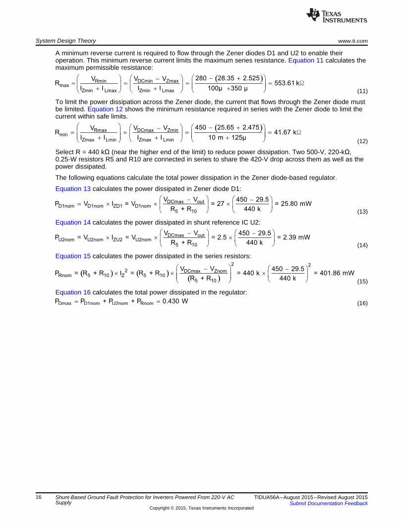
A minimum reverse current is required to flow through the Zener diodes D1 and U2 to enable theiroperation. This minimum reverse current limits the maximum series resistance. Equation 11 calculates themaximum permissible resistance:
(11)
To limit the power dissipation across the Zener diode, the current that flows through the Zener diode mustbe limited. Equation 12 shows the minimum resistance required in series with the Zener diode to limit thecurrent within safe limits.
(12)
Select R = 440 kΩ (near the higher end of the limit) to reduce power dissipation. Two 500-V, 220-kΩ,0.25-W resistors R5 and R10 are connected in series to share the 420-V drop across them as well as thepower dissipated.
The following equations calculate the total power dissipation in the Zener diode-based regulator.
Equation 13 calculates the power dissipated in Zener diode D1:
(13)
Equation 14 calculates the power dissipated in shunt reference IC U2:
(14)
Equation 15 calculates the power dissipated in the series resistors:
(15)
Equation 16 calculates the total power dissipated in the regulator:(16)
16 Shunt-Based Ground Fault Protection for Inverters Powered From 220-V AC TIDUA56A–August 2015–Revised August 2015Supply Submit Documentation Feedback
Copyright © 2015, Texas Instruments Incorporated

9out REF R18
12
RV V V
R
æ öç ÷è
=ø
-
9 9out REF in_p in_n
12 12
R RV V + V V
R R
æ ö æ öç ÷ ç ÷
ø-
è ø è=
( )( )
( )( )
14 12 9 16 12 9 9out REF in_p in_n
12 14 16 14 16 12 12
R R + R R R + R RV = V + V V
R R + R R + R R R
æ ö æ ö æ öç ÷ ç ÷ ç ÷ç ÷ ç ÷ è øè ø
-è ø
P3P3V
GND
100pF
C8
J5
3267
J4
3267
I_LS
VREF_1P65V
TP3
0.005R18
GND
7
5
6
48
U3BOPA2376AID
GND
16.0k
R9
38.3
R25
0.1µFC18
1.00k
R12
1.00k
R14
16.0k
R16
www.ti.com System Design Theory
5.2 Low-Side Current Measurement Solution
5.2.1 DesignFigure 10 shows the low-side current sensing circuit. The difference amplifier topology is used formeasuring the voltage drop across the low-side shunt resistor R14.
Figure 10. Low-Side Current Measurement Circuit
The criteria for selecting the low-side current sense resistor R18 is the same as the criteria for selectingthe high-side current sense resistor. Thus the low-side current sense resistor is selected to be 5 mΩ with3 W.
The transfer function of the difference amplifier is given by Equation 17. Refer to Figure 10 for thereference designators.
(17)
Using the following values where VREF = 1.65 V, R14 = R12, and R16 = R9, Equation 17 simplifies toEquation 18:
where• Vin_p is the non-inverting input of the difference amplifier• Vin_n is the inverting input of the difference amplifier (18)
Vin_p − Vin_n = VR18 is the voltage drop across the low-side shunt resistor R18. Vin_p is connected to GNDand Vin_n is connected across R14 with respect to GND to obtain the inverted output. Section 5.3 explainsthe reason for the inverted output. Equation 18 simplifies to Equation 19:
(19)
17TIDUA56A–August 2015–Revised August 2015 Shunt-Based Ground Fault Protection for Inverters Powered From 220-V ACSupplySubmit Documentation Feedback
Copyright © 2015, Texas Instruments Incorporated

( )out DClink 18V 1.65 16 I R- ´= ´
System Design Theory www.ti.com
The ±20-A current that flows through shunt resistor R18 creates a voltage drop of ±100 mV across theentire resistor. This range must be converted into a 0- to 3.3-V dynamic input range of the ADC. UsingVREF, the 0 A is level shifted to 1.65 V and a gain of 16 is selected to map ±100 mV to ±1.6 V around 1.65V. Equation 19 simplifies to Equation 20:
where• IDClink is the DC bus current (20)
When the DC bus current changes from −20 A to +20 A, the output changes from 3.25 V to 50 mV. TheOPA2376 output voltage swing is limited up to 20 mV from the rails and 40 mV overtemperature. Becauseof these limitations, the output voltage must be limited to 50 mV from the rails.
5.2.2 Simulation Results Using TINA-TI™ Software From TIThe DC bus current is simulated with the help of a current source, I_DC_BUS. The current that flowsthrough shunt resistor R18 in Figure 11 is varied linearly and the output V_lowside_sense is monitored.
Figure 11. Low-Side Current Sense Amplifier
18 Shunt-Based Ground Fault Protection for Inverters Powered From 220-V AC TIDUA56A–August 2015–Revised August 2015Supply Submit Documentation Feedback
Copyright © 2015, Texas Instruments Incorporated

www.ti.com System Design Theory
The DC bus current is varied from 20 A to −20 A linearly from 5 ms to 15 ms. Figure 12 shows thevariation of low-side sense voltage.
Figure 12. Simulation Results for Low-Side Current Sense Amplifier
19TIDUA56A–August 2015–Revised August 2015 Shunt-Based Ground Fault Protection for Inverters Powered From 220-V ACSupplySubmit Documentation Feedback
Copyright © 2015, Texas Instruments Incorporated

0.1µF
C10
GND
P3P3V
GND
GND_FAULT
GND
P3P3V
I_LS
I_HS
GND
P3P3V
GND
P3P3V
5
6
7B
V+
V-
84
U5BTLC372IDR
2
3
1A
V+
V-
84
U5A
TLC372IDR
15.0kR15
P3P3V
16.0kR11
16.0kR23
16.2kR13
16.2kR22
GND
GND
GND
16.2kR17
16.2kR21
0R27
0R28
TP5
820pFC16
820pFC17
820pFC19
5.11M
R31
0R33
0R34
System Design Theory www.ti.com
5.3 Ground Fault Detect ComparatorFigure 13 shows the comparator circuit used to detect the ground fault. The comparator triggers when thedifference between the high-side current and the low-side current is more than the set threshold (±300 mAin this case). Window comparators are used for this functionality. The upper comparator detects when thehigh-side current exceeds the low-side current by 300 mA and the lower comparator detects if the high-side current is less than the low-side current by 300 mA. The TIDA-00442 design uses the TLC372device, which contains dual comparators in a single package, a fast response time, and an open-drainoutput, which helps to logic AND the outputs of the two comparators with the help of a single pullupresistor R20.
Figure 13. GND Fault Comparator Circuit
20 Shunt-Based Ground Fault Protection for Inverters Powered From 220-V AC TIDUA56A–August 2015–Revised August 2015Supply Submit Documentation Feedback
Copyright © 2015, Texas Instruments Incorporated

( ) ( )mid
I_HS + I_LSV
2=
( ) ( )
( )21 17
mid17 21
I_HS R + I_LS RV
R + R
´ ´=
23
23 22
R 16 kVlth 3.3 3.3 1.6398
R + R 16 k + 16.2 k
æ ö æ ö= ´ = ´ =ç ÷ ç ÷
è øè ø
13
13 11
R 16.2 kVuth 3.3 3.3 = 1.6602
R + R 16.2 k + 16 k
æ ö æ ö= ´ = ´ç ÷ ç ÷
è øè ø
REFLower threshold V Threshold voltage 1.65 0.012 1.638 V= - = - =
REFUpper threshold V + Threshold voltage 1.65 + 0.012 1.662 V= = =
300 mA 5 m 16Threshold voltage = 0.012 V
2
´ W ´=
Ground fault current to be detected Shunt resistor GainThreshold voltage
2
´ ´
=
www.ti.com System Design Theory
The average of the high-side and low-side current sense voltages (Vmid) is compared with the upperthreshold voltage and lower threshold voltage. Select the threshold voltage using the followingEquation 21.
(21)
Insert the values for a 300-mA ground fault limit in Equation 21 to calculate Equation 22, Equation 23, andEquation 24:
(22)
(23)
(24)
Resistor divider networks are used to generate the upper and lower threshold voltages from the 3.3-Vsupply. Resistors R11 and R13 generate the upper threshold voltage and R22 and R23 generate thelower threshold voltage. Use resisors R33 and R34 to finely calibrate the threshold voltage manually. R31is the hysteresis setting resistor. The transfer functions of the high-side current sense circuit and the low-side current sense circuit have the same slope but different signs. The transfer function is set up this wayso that the average of both circuits remain the same for any value of current flowing through them in thenormal operating condition, as Equation 28 shows. The ideal average of the high-side and low-sidecurrent sense outputs is exactly 1.65 V, but due to offset and gain errors in both the signal paths, theactual average will deviate from this voltage. The threshold resistor values must be calibrated during theboard testing. The comparator output provides indication of the earth fault, which can be connected to theinterrupt of the MCU. On an interrupt, the MCU can acquire both the high-side and low-side current sensevoltages, calibrate the sensed values, and estimate the accurate value of the ground fault current.
Equation 25 calculates the upper threshold voltage:
(25)
Equation 26 calculate the lower threshold voltage:
(26)
Equation 27 solves for Vmid, which is the voltage at the junction of resistors R13 and R17:
(27)
If R17 = R21, then Vmid becomes the average of I_HS and I_LS (see Equation 28), which is ideally 1.65 V:
(28)
The TLC372 device has an open-drain output. In the normal operating condition, Vmid is between the upperand lower thresholds. In this case both the comparators are in the open-drain output condition and theoutputs are tied together and pulled up to 3.3 V through R15. If the Vmid signal moves either above theupper threshold or below the lower threshold, the output of the respective comparator is pulled down tozero. Select R15 to be large enough to limit the power dissipation during this state.
21TIDUA56A–August 2015–Revised August 2015 Shunt-Based Ground Fault Protection for Inverters Powered From 220-V ACSupplySubmit Documentation Feedback
Copyright © 2015, Texas Instruments Incorporated

VBIAS1
GND2
EN3
VIN4
VREF5
U6
REF2033AIDDCR
GND
VREF_1P65V
P3P3V
P5V
GND
0.1µFC12
0.1µFC11
0.1µFC13
TP4
1
2
J8
282834-2
System Design Theory www.ti.com
5.4 Power Supply and Reference SectionIn this application a bipolar signal (bidirectional DC link current) must be sensed using a unipolar powersupply. To sense the bipolar signal using a unipolar power supply, the user must level shift the output ofthe signal conditioning stages to the midpoint of the power supply rail. A voltage reference is required tobias the signal conditioning stage outputs to the middle of the ADC dynamic range. The REF2033 ICprovides both the 3.3-V supply to the op-amps as well as the 1.65-V reference voltage for biasing thesignal to the middle of the ADC range. Both the outputs of the REF2033 IC can sink or source 20 mA. Thetracking between the 3.3-V supply and 1.65-V supply is excellent and both the supplies are available in asingle, tiny SOT23-5 package that reduces the BOM count and board size.
Figure 14 shows the power supply section.
Figure 14. Power Supply and Reference Circuit
The IC is supplied with a 5-V power supply. The outputs are 3.3 V and 1.65 V. Place 0.1-µF noisedecoupling capacitors close to the IC pins for a clean power input and output rails.
Table 2 shows the load on both the 3.3-V supply as well as the 1.65-V bias source.
Table 2. Power Supply Load Calculation for TIDA00442
MAX CURRENT POWERNAME OF IC OR POWER SUPPLY OR TOTAL OUTPUTSI NO TAKEN BY THE IC CONSUMPTIONCOMPONENT REFERENCE USED CURRENT (mA)(mA) (mW)1 OPA2376 3.3 V 2.29 7.5572 TLC372 3.3 V 0.4 1.32
3.115Comparator output pullup3 3.3 V 0.22 0.726resistor R154 Comparator input references 3.3 V 0.205 0.67655 OPA2376 1.65 V 0.097 0.16 0.097
The maximum load on a 3.3-V supply is 3.115 mA and the total load on a 1.65-V supply is 97 µA. TheTIDA-00442 design uses a REF2033 IC with a sink and source capability of 20 mA.
22 Shunt-Based Ground Fault Protection for Inverters Powered From 220-V AC TIDUA56A–August 2015–Revised August 2015Supply Submit Documentation Feedback
Copyright © 2015, Texas Instruments Incorporated

Rhs
Rls
Hi-side current sense
Low-side current senseOPA2376
Low side current sensing
and output level shifting
difference amplifier
DC+
DCí
Voltage follower
buffer
INA170 OPA2376
310-V DC
power
supply
Variable load
www.ti.com Test Data
6 Test DataThe TIDA-00442 board can be used with a DC bus voltage of up to 450-V DC. This specification includes100-V AC or 110-V AC mains-powered drives as well as 220-V AC mains-powered drives. Therefore theboard test results are split into two sections for the 310-V DC bus voltage (220-V AC mains-powereddrives) as well as the 170-V DC bus voltage (110-V AC mains-powered drives).
The following tests are carried out on the design:• High-side and low-side current measurement error• Measurement error across different DC link voltages• Measurement error across operating temperatures from −10°C to 55°C• Detection of ground fault scenario and response time• Testing on C2000 motor control kit for ground fault operation
6.1 Test Results for 310-V DC Bus Voltage (220-V AC Mains-Powered Drives)
6.1.1 High-Side and Low-Side Current Measurement ErrorFigure 15 shows the test setup for measuring the error in high-side and low-side current measurementcircuits. A variable load is connected to a high-voltage DC power supply through the TIDA-00442 board.An external DC power supply supplies the 5 V to power up the board. The high-voltage DC power supply(which simulates the DC bus voltage in the actual drive) is set to 310-V DC. The load is varied from −5 Ato +5 A with the help of the variable electronic load and the high-side and low-side current measurementoutputs are recorded.
Figure 15. Test Setup for TIDA-00442 High-Side and Low-Side Current Measurement Error
23TIDUA56A–August 2015–Revised August 2015 Shunt-Based Ground Fault Protection for Inverters Powered From 220-V ACSupplySubmit Documentation Feedback
Copyright © 2015, Texas Instruments Incorporated
DC Bus Current (A)
Err
or
-5 -4 -3 -2 -1 0 1 2 3 4 5-0.8%-0.7%-0.6%-0.5%-0.4%-0.3%-0.2%-0.1%
00.1%0.2%0.3%0.4%0.5%0.6%
D001
High-Side Current SenseLow-Side Current Sense
DC Bus Current (A)
Err
or
-5 -4 -3 -2 -1 0 1 2 3 4 5-0.5%
-0.4%
-0.3%
-0.2%
-0.1%
0
0.1%
0.2%
0.3%
0.4%
0.5%
D002
Calibrated High-Side Current SenseCalibrated Low-Side Current Sense
Test Data www.ti.com
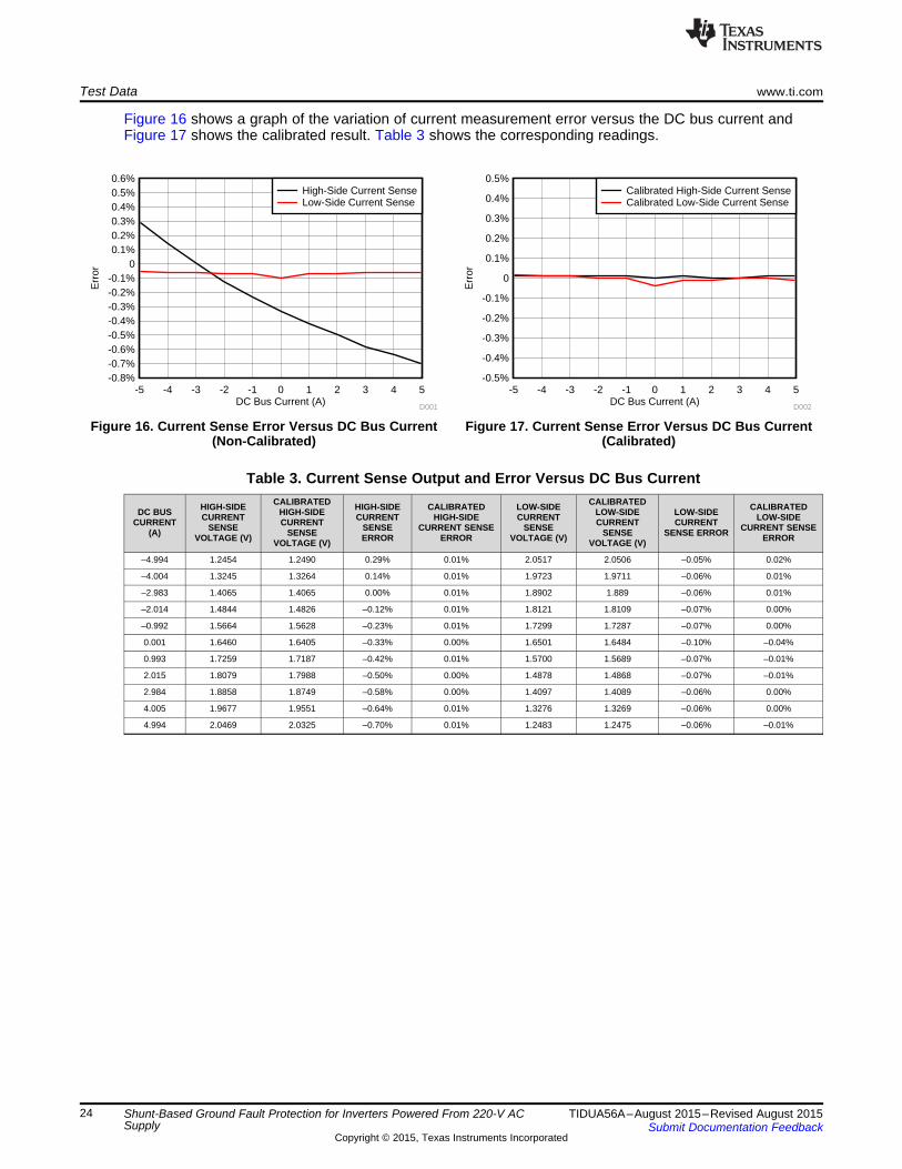
Figure 16 shows a graph of the variation of current measurement error versus the DC bus current andFigure 17 shows the calibrated result. Table 3 shows the corresponding readings.
Figure 16. Current Sense Error Versus DC Bus Current Figure 17. Current Sense Error Versus DC Bus Current(Non-Calibrated) (Calibrated)
Table 3. Current Sense Output and Error Versus DC Bus CurrentCALIBRATED CALIBRATEDHIGH-SIDE HIGH-SIDE CALIBRATED LOW-SIDE CALIBRATEDDC BUS HIGH-SIDE LOW-SIDE LOW-SIDECURRENT CURRENT HIGH-SIDE CURRENT LOW-SIDECURRENT CURRENT CURRENT CURRENTSENSE SENSE CURRENT SENSE SENSE CURRENT SENSE(A) SENSE SENSE SENSE ERRORVOLTAGE (V) ERROR ERROR VOLTAGE (V) ERRORVOLTAGE (V) VOLTAGE (V)
–4.994 1.2454 1.2490 0.29% 0.01% 2.0517 2.0506 –0.05% 0.02%
–4.004 1.3245 1.3264 0.14% 0.01% 1.9723 1.9711 –0.06% 0.01%
–2.983 1.4065 1.4065 0.00% 0.01% 1.8902 1.889 –0.06% 0.01%
–2.014 1.4844 1.4826 –0.12% 0.01% 1.8121 1.8109 –0.07% 0.00%
–0.992 1.5664 1.5628 –0.23% 0.01% 1.7299 1.7287 –0.07% 0.00%
0.001 1.6460 1.6405 –0.33% 0.00% 1.6501 1.6484 –0.10% –0.04%
0.993 1.7259 1.7187 –0.42% 0.01% 1.5700 1.5689 –0.07% –0.01%
2.015 1.8079 1.7988 –0.50% 0.00% 1.4878 1.4868 –0.07% –0.01%
2.984 1.8858 1.8749 –0.58% 0.00% 1.4097 1.4089 –0.06% 0.00%
4.005 1.9677 1.9551 –0.64% 0.01% 1.3276 1.3269 –0.06% 0.00%
4.994 2.0469 2.0325 –0.70% 0.01% 1.2483 1.2475 –0.06% –0.01%
24 Shunt-Based Ground Fault Protection for Inverters Powered From 220-V AC TIDUA56A–August 2015–Revised August 2015Supply Submit Documentation Feedback
Copyright © 2015, Texas Instruments Incorporated

DC Bus Voltage (V)
Err
or
100 140 180 220 260 300 340 380
-0.5%
-0.48%
-0.46%
-0.44%
-0.42%
-0.4%
-0.38%
-0.36%
-0.34%
-0.32%
-0.3%
D003
High-Side Current Sense (2 A)
High-Side Current Sense (1 A)
www.ti.com Test Data
6.1.2 High-Side Measurement Error Across Different DC Link VoltagesFigure 18 shows the variation of high-side current measurement error with DC bus voltage and Table 4shows the tabulated test results. The user can observe that there is little variation in the high-side errorwith variation in the DC bus voltage. This lack of variation is because the low-side, buck converter powersupply for the INA170 device always maintains the floating reference 30 V below the DC bus. So althoughthe DC bus voltage changes, the common-mode input observed by the INA170 inputs is constant.
Figure 18. High-Side Current Measurement Error Versus DC Bus Voltage (Non-Calibrated)
Table 4. High-Side Current Sense Voltage and Error Versus DC Bus Voltage (V)
HIGH-SIDE CURRENT HIGH-SIDE CURRENT HIGH-SIDE CURRENT HIGH-SIDE CURRENTDC BUS VOLTAGE SENSE VOLTAGE AT SENSE ERROR SENSE VOLTAGE SENSE ERROR(V) 1 A (V) AT 1 A AT 2 A (V) AT 2 A100 1.7191 –0.36% 1.7993 –0.43%120 1.7191 –0.36% 1.7993 –0.44%150 1.719 –0.37% 1.7994 –0.43%200 1.7192 –0.35% 1.7994 –0.43%250 1.7193 –0.35% 1.7994 –0.43%275 1.7193 –0.35% 1.7994 –0.43%300 1.7193 –0.35% 1.7994 –0.43%350 1.7194 –0.35% 1.7995 –0.43%400 1.7194 –0.35% 1.7995 –0.43%
25TIDUA56A–August 2015–Revised August 2015 Shunt-Based Ground Fault Protection for Inverters Powered From 220-V ACSupplySubmit Documentation Feedback
Copyright © 2015, Texas Instruments Incorporated

DC Bus Current (A)
Err
or
-6 -5 -4 -3 -2 -1 0 1 2 3 4 5 6
-0.8%
-0.7%
-0.6%
-0.5%
-0.4%
-0.3%
-0.2%
-0.1%
0
0.1%
0.2%
0.3%
0.4%
0.5%
0.6%
0.7%
0.8%
D004
High-Side Current Sense (-10°C)
High-Side Current Sense (25°C)
High-Side Current Sense (55°C)
Test Data www.ti.com
6.1.3 Measurement Error Versus TemperatureThis test shows the variation of the signal-conditioning circuit output overtemperature. During thismeasurement, the board remains inside a temperature chamber and is tested at −10°C, 25°C, and 55°C.Figure 19 shows the variation of the high-side measurement error and Table 5 shows the correspondingresults. Figure 20 shows the variation of the low-side measurement error and Table 6 shows thecorresponding results.
Figure 19. Graph of High-Side Current Measurement Error at −10°C, 25°C, and 55°C (Non-Calibrated)
Table 5. High-Side Current Sense Voltage and measurement error Versus DC Bus Currentat −10°C, 25°C, and 55°C
–10°C 25°C 55°CHIGH-SIDE HIGH-SIDE HIGH-SIDE HIGH-SIDE HIGH-SIDE HIGH-SIDECURRENTDC BUS CURRENT DC BUS CURRENT CURRENT DC BUS CURRENT CURRENTSENSECURRENT SENSE CURRENT SENSE SENSE CURRENT SENSE SENSEVOLTAGE(A) ERROR AT (A) VOLTAGE ERROR AT (A) VOLTAGE ERROR ATAT −10°C −10°C AT 25°C (V) 25°C AT 55°C (V) 55°C(V)
–4.965 1.2487 –0.02% –4.994 1.249 0.19% –5.027 1.2492 0.42%–3.9783 1.3262 –0.12% –4.004 1.3264 0.05% –4.0359 1.3268 0.27%–2.9866 1.404 –0.22% –2.983 1.4065 –0.07% –2.9861 1.4091 0.13%–2.0163 1.4802 –0.31% –2.014 1.4826 –0.16% –2.0148 1.4853 0.03%–0.9948 1.5605 –0.38% –0.992 1.5628 –0.25% –0.993 1.5654 –0.08%0.0016 1.6385 –0.47% 0.001 1.6405 –0.34% 0.0016 1.6433 –0.18%0.9936 1.7165 –0.53% 0.993 1.7187 –0.40% 0.9895 1.7209 –0.25%2.0152 1.7968 –0.58% 2.015 1.7988 –0.47% 1.9744 1.7981 –0.33%2.987 1.8732 –0.63% 2.984 1.8749 –0.53% 2.9937 1.878 –0.40%3.9785 1.951 –0.68% 4.005 1.9551 –0.58% 4.025 1.9589 –0.47%4.971 2.0288 –0.73% 4.994 2.0325 –0.64% 4.8943 2.0269 –0.53%
26 Shunt-Based Ground Fault Protection for Inverters Powered From 220-V AC TIDUA56A–August 2015–Revised August 2015Supply Submit Documentation Feedback
Copyright © 2015, Texas Instruments Incorporated

DC Bus Current (A)
Err
or
-6 -5 -4 -3 -2 -1 0 1 2 3 4 5 6
-0.5%
-0.4%
-0.3%
-0.2%
-0.1%
0
0.1%
0.2%
0.3%
0.4%
0.5%
D005
Low-Side Current Sense (-10°C)
Low-Side Current Sense (25°C)
Low-Side Current Sense (55°C)
www.ti.com Test Data
Figure 20. Graph of Low-Side Measurement Error at −10°C, 25°C, and 55°C (Non-Calibrated)
Table 6. Low-Side Current Sense Voltage and Measurement Error Versus DC Bus Currentat −10°C, 25°C, and 55°C
–10°C 25°C 55°CHIGH-SIDE HIGH-SIDE HIGH-SIDE HIGH-SIDE HIGH-SIDE HIGH-SIDECURRENTDC BUS CURRENT DC BUS CURRENT CURRENT DC BUS CURRENT CURRENTSENSECURRENT SENSE CURRENT SENSE SENSE CURRENT SENSE SENSEVOLTAGE(A) ERROR AT (A) VOLTAGE ERROR AT (A) VOLTAGE ERROR ATAT −10°C −10°C AT 25°C (V) 25°C AT 55°C (V) 55°C(V)
–4.965 2.0482 –0.05% –4.994 2.0506 –0.05% –5.027 2.0529 –0.06%–3.9783 1.9688 –0.05% –4.004 1.9711 –0.06% –4.0359 1.974 –0.03%–2.9866 1.8891 –0.06% –2.983 1.889 –0.06% –2.9861 1.8895 –0.03%–2.0163 1.811 –0.06% –2.014 1.8109 –0.07% –2.0148 1.8113 –0.05%–0.9948 1.7288 –0.06% –0.992 1.7287 –0.07% –0.993 1.7291 –0.05%0.0016 1.6482 –0.11% 0.001 1.6484 –0.10% 0.0016 1.6486 –0.08%0.9936 1.5689 –0.08% 0.993 1.5689 –0.07% 0.9895 1.5695 –0.06%2.0152 1.4869 –0.07% 2.015 1.4868 –0.07% 1.9744 1.4903 –0.05%2.987 1.4089 –0.06% 2.984 1.4089 –0.06% 2.9937 1.4084 –0.06%3.9785 1.3293 –0.06% 4.005 1.3269 –0.06% 4.025 1.3252 –0.07%4.971 1.2497 –0.06% 4.994 1.2475 –0.06% 4.8943 1.2554 –0.08%
27TIDUA56A–August 2015–Revised August 2015 Shunt-Based Ground Fault Protection for Inverters Powered From 220-V ACSupplySubmit Documentation Feedback
Copyright © 2015, Texas Instruments Incorporated

TIDA-00442GND fault detection
Circuit power supplies
310-V DC power supplyConstant load
DC+
DCí
Variable electronic load
5 V
Test Data www.ti.com
6.1.4 Detection of GND Fault Scenario and Response TimeThis section shows the detection of the GND fault scenario. Figure 21 shows the setup for simulating theGND fault. A constant electrical load is connected on the output of the TIDA-00442 board. One side of avariable electronic load is connected to the constant load and the other side is connected to DC− so that itbypasses the TIDA-00442 board. The variable electronic load is used to simulate the earth leakage faultcurrent. The constant load is set to 86 mA in the test setup. The variable electronic load is a square waveof 100 Hz and has a 350-mA peak.
Figure 21. Setup for Creation of GND Fault Scenario
28 Shunt-Based Ground Fault Protection for Inverters Powered From 220-V AC TIDUA56A–August 2015–Revised August 2015Supply Submit Documentation Feedback
Copyright © 2015, Texas Instruments Incorporated
www.ti.com Test Data
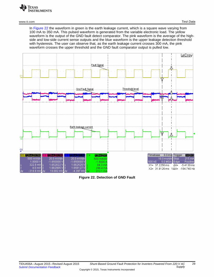
In Figure 22 the waveform in green is the earth leakage current, which is a square wave varying from100 mA to 350 mA. This pulsed waveform is generated from the variable electronic load. The yellowwaveform is the output of the GND fault detect comparator. The pink waveform is the average of the high-side and low-side current sense outputs and the blue waveform is the upper leakage detection thresholdwith hysteresis. The user can observe that, as the earth leakage current crosses 300 mA, the pinkwaveform crosses the upper threshold and the GND fault comparator output is pulled low.
Figure 22. Detection of GND Fault
29TIDUA56A–August 2015–Revised August 2015 Shunt-Based Ground Fault Protection for Inverters Powered From 220-V ACSupplySubmit Documentation Feedback
Copyright © 2015, Texas Instruments Incorporated

Test Data www.ti.com
Figure 23 shows the response time to the GND fault. A zoomed-in version is also available so the usercan read the response time. The response time in this scenario shows to be 32 µs.
Figure 23. Response Time to GND Fault
30 Shunt-Based Ground Fault Protection for Inverters Powered From 220-V AC TIDUA56A–August 2015–Revised August 2015Supply Submit Documentation Feedback
Copyright © 2015, Texas Instruments Incorporated

TIDA-00442GND fault detection
Circuit power supplies
310-V DC power supply
DC+
DCí
Variable electronic load
5 V
High voltage motor control kit
GUI running on PC
USB
Motor
www.ti.com Test Data
6.1.5 Testing With C2000™ MCU-Based High-Voltage Motor Control Kit From TI to Detect GND FaultThis test uses the TIDA-00442 board to detect the GND fault on an actual motor drive. The C2000application kit for high-voltage motor control applications is used as the motor driver. A three-phase ACinduction motor is connected to the drive. Figure 24 shows a block diagram of the setup.
Figure 25 and Figure 26 show the actual setup images. The DC power supply is connected to the drivethrough the TIDA-00442 board. Figure 27 shows the graphical user interface (GUI), which is used tocontrol the motor. Connect the PC to the motor control kit through a USB, power on the DC supply to thedrive, select the motor type (either permanent magnet synchronous motor (PMSM) or AC induction motor(ACIM)), and enable the motor if none of the faults are flagged in the GUI software. Detailed informationabout the high-voltage motor control application kit and the GUI are available by downloading the TIcontrolSUITE™ software
Figure 24. Block Diagram of C2000 High-Voltage Motor Drive Setup
31TIDUA56A–August 2015–Revised August 2015 Shunt-Based Ground Fault Protection for Inverters Powered From 220-V ACSupplySubmit Documentation Feedback
Copyright © 2015, Texas Instruments Incorporated

TIDA-00442
Test Data www.ti.com
Figure 25. C2000 High-Voltage Motor Drive Setup
Figure 26. TIDA-00442 C2000™ MCU-Based High-Voltage Motor Control Kit From TI
32 Shunt-Based Ground Fault Protection for Inverters Powered From 220-V AC TIDUA56A–August 2015–Revised August 2015Supply Submit Documentation Feedback
Copyright © 2015, Texas Instruments Incorporated

www.ti.com Test Data
Figure 27. GUI to Control AC Motor
33TIDUA56A–August 2015–Revised August 2015 Shunt-Based Ground Fault Protection for Inverters Powered From 220-V ACSupplySubmit Documentation Feedback
Copyright © 2015, Texas Instruments Incorporated

Fault signal
Earth leakage current
Test Data www.ti.com
Figure 28 shows the test result. The yellow waveform is the earth leakage current with a frequency of100 Hz and it varies from a 100- to 350-mA peak. The response time is 23.8 µs. The motor runs at 1000rpm from a DC bus voltage of 310 V.
Figure 28. GND Fault Response Time
34 Shunt-Based Ground Fault Protection for Inverters Powered From 220-V AC TIDUA56A–August 2015–Revised August 2015Supply Submit Documentation Feedback
Copyright © 2015, Texas Instruments Incorporated

DC Bus Current (A)
Err
or
-5 -4 -3 -2 -1 0 1 2 3 4 5
-0.8%
-0.7%
-0.6%
-0.5%
-0.4%
-0.3%
-0.2%
-0.1%
0
0.1%
0.2%
0.3%
0.4%
0.5%
0.6%
D006
High-Side Current Sense
Low-Side Current Sense
DC Bus Current (A)
Err
or
-5 -4 -3 -2 -1 0 1 2 3 4 5
-0.5%
-0.4%
-0.3%
-0.2%
-0.1%
0
0.1%
0.2%
0.3%
0.4%
0.5%
D007
Calibrated High-Side Current Sense
Calibrated Low-Side Current Sense
170-V DC power supply
INA170
OPA2376
OPA2376
Rhs
Rls
High-side current sense
Voltage follower buffer
Low side current sensing and output level shifting
difference amplifier
Variable load
DC+
DCí
Low-side current sense
www.ti.com Test Data
6.2 Test Results for 170-V DC Bus Voltage (110-V AC Mains-Powered Drives)
6.2.1 High-Side and Low-Side Current Measurement ErrorFigure 29 shows the test setup for measuring the error of the high-side and low-side current measurementcircuit. A variable load is connected to a high-voltage DC power supply through the TIDA-00442 board. Anexternal DC power supply provides 5 V to power up the board. The high voltage DC power supply, whichsimulates the DC bus voltage in the actual drive, is set to 170-V DC. The load is varied from −5 A to 5 Awith the help of the variable electronic load and the high-side and low-side current measurement outputsare recorded.
Figure 29. Test Setup for TIDA-00442 High-Side and Low-Side Current Measurement Error
Figure 30 shows a graph of the variation of current measurement error versus the DC bus current andFigure 31 shows the calibrated result. Table 7 shows the corresponding readings.
Figure 30. Current Sense error Versus DC Bus Current Figure 31. Current Sense Error Versus DC Bus Current(Non-Calibrated) (Calibrated)
35TIDUA56A–August 2015–Revised August 2015 Shunt-Based Ground Fault Protection for Inverters Powered From 220-V ACSupplySubmit Documentation Feedback
Copyright © 2015, Texas Instruments Incorporated

Test Data www.ti.com
Table 7. Current Sense Output and Measurement error Versus DC Bus CurrentCALIBRATED CALIBRATED CALIBRATED CALIBRATEDHIGH-SIDE HIGH-SIDE LOW-SIDE LOW-SIDEHIGH-SIDE HIGH-SIDE LOW-SIDE LOW-SIDEDC BUS CURRENT CURRENT CURRENT CURRENTCURRENT CURRENT CURRENT CURRENTCURRENT (A) SENSE SENSE ERROR SENSE SENSE ERRORSENSE SENSE ERROR SENSE SENSE ERRORVOLTAGE (V) (%) VOLTAGE (V) (%)VOLTAGE (V) (%) VOLTAGE (V) (%)
–5.01 1.2438 1.2475 0.29% 0.00% 2.0532 2.0535 0.01% 0.04%
–3.991 1.3256 1.3274 0.13% 0.00% 1.9712 1.9714 0.01% 0.03%
–3.003 1.4050 1.4049 –0.01% –0.01% 1.8917 1.8917 0.00% 0.02%
–2.012 1.4845 1.4826 –0.13% –0.01% 1.8119 1.8118 –0.01% 0.00%
–0.991 1.5666 1.5628 –0.24% –0.01% 1.7297 1.7295 –0.01% 0.00%
0.001 1.6460 1.6405 –0.34% 0.00% 1.6500 1.6477 –0.14% –0.14%
0.99 1.7257 1.7182 –0.44% –0.01% 1.5702 1.5701 –0.01% –0.01%
2.012 1.8079 1.7985 –0.52% –0.01% 1.4878 1.4881 0.02% 0.01%
3.003 1.8875 1.8763 –0.59% 0.00% 1.4081 1.4086 0.04% 0.02%
3.991 1.9669 1.9539 –0.66% 0.00% 1.3285 1.3292 0.05% 0.02%
5.011 2.0487 2.0339 –0.72% 0.00% 1.2464 1.2474 0.08% 0.04%
36 Shunt-Based Ground Fault Protection for Inverters Powered From 220-V AC TIDUA56A–August 2015–Revised August 2015Supply Submit Documentation Feedback
Copyright © 2015, Texas Instruments Incorporated

DC Bus Current (A)
Err
or
-6 -5 -4 -3 -2 -1 0 1 2 3 4 5 6
-0.8%
-0.7%
-0.6%
-0.5%
-0.4%
-0.3%
-0.2%
-0.1%
0
0.1%
0.2%
0.3%
0.4%
0.5%
0.6%
0.7%
0.8%
D008
High-Side Current Sense (-10°C)
High-Side Current Sense (25°C)
High-Side Current Sense (55°C)
www.ti.com Test Data
6.2.2 Measurement Error Versus TemperatureThis test identifies the variation of the signal-conditioning circuit measurement error overtemperature. Theboard remains inside a temperature chamber and is tested at −10°C, 25°C, and 55°C. Figure 32 showsthe variation of the high-side measurement error and Table 8 shows the corresponding results.
Figure 32. Graph of High-Side Current Measurement Error at −10°C, 25°C, and 55°C (Non-Calibrated)
Table 8. High-Side Current Sense Voltage and Measurement Error Versus DC Bus Current at−10°C, 25°C, and 55°C
–10°C 25°C 55°CHIGH-SIDE HIGH-SIDE HIGH-SIDE HIGH-SIDE HIGH-SIDE HIGH-SIDECURRENTDC BUS CURRENT DC BUS CURRENT CURRENT DC BUS CURRENT CURRENTSENSECURRENT SENSE CURRENT SENSE SENSE CURRENT SENSE SENSEVOLTAGE(A) ERROR AT (A) VOLTAGE ERROR AT (A) VOLTAGE ERROR ATAT −10°C −10°C (%) AT 25°C (V) 25°C (%) AT 55°C (V) 55°C (%)(V)
–5.0122 1.2449 –0.02% –5.01 1.2475 0.18% –5.0124 1.2503 0.42%–3.993 1.3249 –0.13% –3.991 1.3274 0.04% –3.9932 1.3302 0.27%
–3.0045 1.4025 –0.23% –3.003 1.4049 –0.07% –3.0045 1.4077 0.14%–2.014 1.4803 –0.31% –2.012 1.4826 –0.17% –2.0139 1.4854 0.03%–0.992 1.5606 –0.39% –0.991 1.5628 –0.26% –0.9918 1.5655 –0.08%0.0009 1.6383 –0.48% 0.00100 164.05% –0.34% 0.0009 1.6431 –0.19%0.9916 1.7164 –0.52% 0.99000 171.82% –0.41% 0.9915 1.721 –0.26%2.0137 1.7966 –0.59% 2.01200 179.85% –0.47% 2.014 1.8012 –0.33%3.0044 1.8745 –0.63% 3.00300 187.63% –0.53% 3.0042 1.8789 –0.40%3.9927 1.9521 –0.68% 3.99100 195.39% –0.58% 3.9922 1.9564 –0.46%5.0121 2.0321 –0.73% 5.01100 203.39% –0.64% 5.011 2.0363 –0.52%
37TIDUA56A–August 2015–Revised August 2015 Shunt-Based Ground Fault Protection for Inverters Powered From 220-V ACSupplySubmit Documentation Feedback
Copyright © 2015, Texas Instruments Incorporated
DC Bus Current (A)
Err
or
-6 -5 -4 -3 -2 -1 0 1 2 3 4 5 6
-1%
-0.8%
-0.6%
-0.4%
-0.2%
0
0.2%
0.4%
0.6%
0.8%
1%
D009
Low-Side Current Sense (-10°C)
Low-Side Current Sense (25°C)
Low-Side Current Sense (55°C)
Test Data www.ti.com
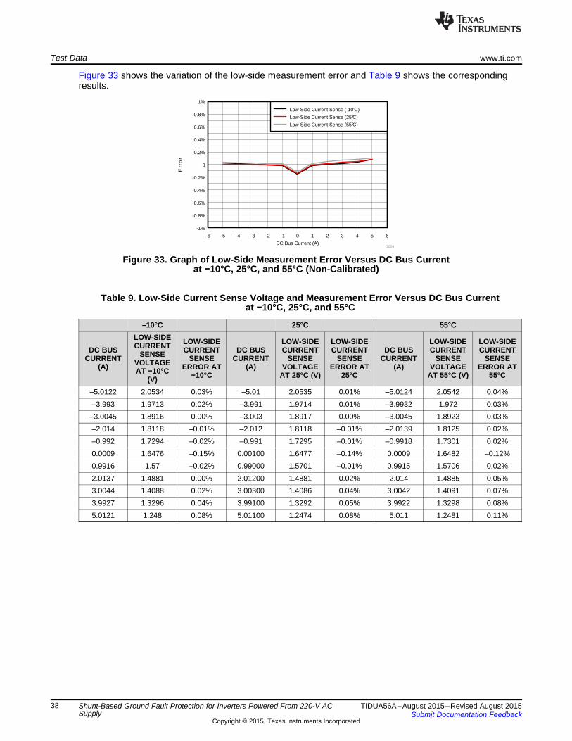
Figure 33 shows the variation of the low-side measurement error and Table 9 shows the correspondingresults.
Figure 33. Graph of Low-Side Measurement Error Versus DC Bus Currentat −10°C, 25°C, and 55°C (Non-Calibrated)
Table 9. Low-Side Current Sense Voltage and Measurement Error Versus DC Bus Currentat −10°C, 25°C, and 55°C
–10°C 25°C 55°CLOW-SIDE LOW-SIDE LOW-SIDE LOW-SIDE LOW-SIDE LOW-SIDECURRENTDC BUS CURRENT DC BUS CURRENT CURRENT DC BUS CURRENT CURRENTSENSECURRENT SENSE CURRENT SENSE SENSE CURRENT SENSE SENSEVOLTAGE(A) ERROR AT (A) VOLTAGE ERROR AT (A) VOLTAGE ERROR ATAT −10°C −10°C AT 25°C (V) 25°C AT 55°C (V) 55°C(V)
–5.0122 2.0534 0.03% –5.01 2.0535 0.01% –5.0124 2.0542 0.04%–3.993 1.9713 0.02% –3.991 1.9714 0.01% –3.9932 1.972 0.03%
–3.0045 1.8916 0.00% –3.003 1.8917 0.00% –3.0045 1.8923 0.03%–2.014 1.8118 –0.01% –2.012 1.8118 –0.01% –2.0139 1.8125 0.02%–0.992 1.7294 –0.02% –0.991 1.7295 –0.01% –0.9918 1.7301 0.02%0.0009 1.6476 –0.15% 0.00100 1.6477 –0.14% 0.0009 1.6482 –0.12%0.9916 1.57 –0.02% 0.99000 1.5701 –0.01% 0.9915 1.5706 0.02%2.0137 1.4881 0.00% 2.01200 1.4881 0.02% 2.014 1.4885 0.05%3.0044 1.4088 0.02% 3.00300 1.4086 0.04% 3.0042 1.4091 0.07%3.9927 1.3296 0.04% 3.99100 1.3292 0.05% 3.9922 1.3298 0.08%5.0121 1.248 0.08% 5.01100 1.2474 0.08% 5.011 1.2481 0.11%
38 Shunt-Based Ground Fault Protection for Inverters Powered From 220-V AC TIDUA56A–August 2015–Revised August 2015Supply Submit Documentation Feedback
Copyright © 2015, Texas Instruments Incorporated

TIDA-00442GND fault detection
Circuit power supplies
170-V DC power supplyConstant load
DC+
DCí
Variable electronic load
5 V
www.ti.com Test Data
6.2.3 Detection of GND Fault Scenario and Response TimeThis section shows the detection of the GND fault scenario. Figure 34 shows the setup for simulating theGND fault. A constant electrical load is connected on the output of the TIDA-00442 board. One side of avariable electronic load is connected to the constant load and the other side is connected to the DC− sothat it bypasses the TIDA-00442 board. The variable electronic load is used to simulate the earth leakagefault current. The constant load is set to 86 mA in this test setup. The variable electronic load is a squarewave of 100 Hz and has a 350 mA peak.
Figure 34. Setup for Creation of GND Fault Scenario
39TIDUA56A–August 2015–Revised August 2015 Shunt-Based Ground Fault Protection for Inverters Powered From 220-V ACSupplySubmit Documentation Feedback
Copyright © 2015, Texas Instruments Incorporated
Test Data www.ti.com
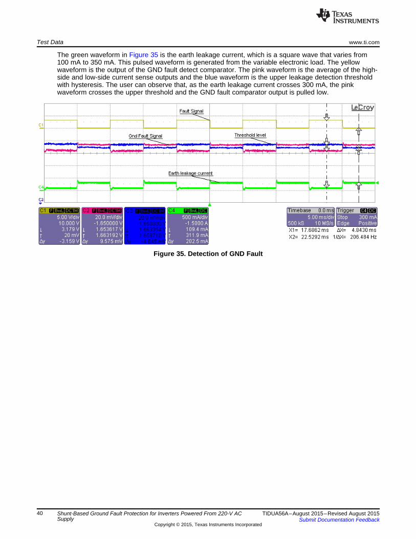
The green waveform in Figure 35 is the earth leakage current, which is a square wave that varies from100 mA to 350 mA. This pulsed waveform is generated from the variable electronic load. The yellowwaveform is the output of the GND fault detect comparator. The pink waveform is the average of the high-side and low-side current sense outputs and the blue waveform is the upper leakage detection thresholdwith hysteresis. The user can observe that, as the earth leakage current crosses 300 mA, the pinkwaveform crosses the upper threshold and the GND fault comparator output is pulled low.
Figure 35. Detection of GND Fault
40 Shunt-Based Ground Fault Protection for Inverters Powered From 220-V AC TIDUA56A–August 2015–Revised August 2015Supply Submit Documentation Feedback
Copyright © 2015, Texas Instruments Incorporated

www.ti.com Test Data
Figure 36 shows the response time to the GND fault. The yellow waveform is the output of the GND faultdetect comparator. When the output is pulled down low, the yellow waveform indicates a GND fault. Thegreen waveform is the earth leakage current, which has a frequency of 100 Hz and varies from 100 mA to350 mA. A zoomed-in version is also available so the user can read the response time. The response timein this scenario shows to be 29.2 µs.
Figure 36. GND Fault Response Time
41TIDUA56A–August 2015–Revised August 2015 Shunt-Based Ground Fault Protection for Inverters Powered From 220-V ACSupplySubmit Documentation Feedback
Copyright © 2015, Texas Instruments Incorporated

Test Data www.ti.com
6.2.4 Testing With C2000™ MCU-Based High-Voltage Motor Control Kit From TI to Detect GND FaultThis test uses the TIDA-00442 board to detect the GND fault on an actual motor drive. The setup is similarto in the setup that Section 6.1.5 shows.
Figure 36 and Figure 38 show the test result. The yellow waveform is the earth leakage current with afrequency of 100 Hz and it varies from a 100-mA to 350-mA peak. The response time is 24.6 µs. Themotor runs at 1000 rpm from a DC bus voltage of 170 V.
Figure 37. GND Fault Signal
42 Shunt-Based Ground Fault Protection for Inverters Powered From 220-V AC TIDUA56A–August 2015–Revised August 2015Supply Submit Documentation Feedback
Copyright © 2015, Texas Instruments Incorporated

www.ti.com Test Data
Figure 38. Zoomed-In GND Fault Signal Showing GND Fault Response Time
43TIDUA56A–August 2015–Revised August 2015 Shunt-Based Ground Fault Protection for Inverters Powered From 220-V ACSupplySubmit Documentation Feedback
Copyright © 2015, Texas Instruments Incorporated

0.1µF
C6
GND
P3P3V
GND
100pF
C1
I_HS
0
R6
TP2TP1
VIN-1
VIN+2
VREF3
GND4
ROS5
OUT6
NC7
V+8
U1
INA170EA/2K5
J1
3267
0.005R1J2
3267
0.1µFC4
1µFC50.1µF
C3
GND
P3P3V
GND
100pF
C8
J5
3267
J4
3267
I_LS
VREF_1P65V
VBIAS1
GND2
EN3
VIN4
VREF5
U6
REF2033AIDDCR
GND
VREF_1P65V
P3P3V
P5V
GND
0.1µFC12
0.1µFC11
0.1µFC13
TP3
TP4
0.005R18
GND 0.1µF
C10
GND
P3P3V
GND
GND_FAULT
GND
P3P3V
I_LS
I_HS
GND
P3P3V
GND
P3P3V
1
2
J3
282834-2
1
2
J6
282834-2
I_HS
GND
I_LS
GND
1
2
J7
282834-2
GND_FAULT
GND
5
6
7B
V+
V-
84
U5BTLC372IDR
2
3
1A
V+
V-
84
U5A
TLC372IDR
15.0kR15
P3P3V
16.0kR11
16.0kR23
NC3
12 U2
LM4040DIM3X-2.5
0.1µFC14
GND1
GND2
FB3
VDD4
HVIN5
NC6
DRAIN8
U7
UCC28880DR
GND
GND
D1STTH1R06A
3
1
2 Q2PBHV9050T,215
FB
FB 51k
R26
402kR10
1.47MR5
200kR8
1
3
2
48
U3AOPA2376AID
7
5
6
48
U3BOPA2376AID
DC_BUS_POS
Float_Ref
Float_Ref
P5V
16.2kR13
16.2kR22
16.0k
R2
GND
GND
GND
GND
GND
16.0k
R9
GND
100pFC15
16.2kR17
16.2kR21
0
R20DNP
0R19
42
1
3
Q1ZVP0545GTA
1 2L1
680 µH
1
2
J8
282834-2
0R27
0R28
TP5
22
R29
0.01µFC7
22
R304.99kR3
0.033µFC20
GND
DC_BUS_POS
VREF_2P5V
VREF_2P5V
0.1µFC9
38.3
R24
820pFC16
820pFC17
820pFC19
38.3
R25
0.1µFC18
1.00k
R12
1.00k
R14
16.0k
R16
16.0kR7
24.3kR410µF
C210µFC21
5.11M
R31
10.0k
R32
1µFC24
0R33
0R34
Design Files www.ti.com
7 Design Files
7.1 SchematicsTo download the schematics for each board, see the design files at TIDA-00442.
Figure 39. Current Sense and Signal Conditioning Schematic
44 Shunt-Based Ground Fault Protection for Inverters Powered From 220-V AC TIDUA56A–August 2015–Revised August 2015Supply Submit Documentation Feedback
Copyright © 2015, Texas Instruments Incorporated

www.ti.com Design Files
7.2 Bill of MaterialsTo download the bill of materials (BOM) for each board, see the design files at TIDA-00442.
7.3 PCB Layout RecommendationsPCB placement and layout is very important to get the specified performance as mentioned in thedatasheet. This board contains high voltage nets. Special care must be taken to provide sufficient spacingbetween high voltage nets and low voltage nets.
7.3.1 Layout Recommendations for High-Side Current Measurement Signal ChainFigure 40 shows the layout for the INA170 current shunt monitor IC, which has the following layoutrecommendations:• Use Kelvin connections for current sense resistor. The input differential filter between the shunt resistor
and the INA170 sense inputs consists of R30, R29, and C7. The routing from the shunt resistor to theINA170 inputs through the differential filter should be symmetrical and as short as possible, place thedifferential filter capacitor C7 very close to the Vin+ and Vin– pins of INA170.
• The decoupling capacitor should be placed close to the power pin of INA170. The floating DC-DCconverter power supply section can be placed farther away from the INA170 circuitry and the powerthen routed to INA170 through power planes.
Figure 40. Layout Recommendations for INA170 Current Sense Circuit
45TIDUA56A–August 2015–Revised August 2015 Shunt-Based Ground Fault Protection for Inverters Powered From 220-V ACSupplySubmit Documentation Feedback
Copyright © 2015, Texas Instruments Incorporated
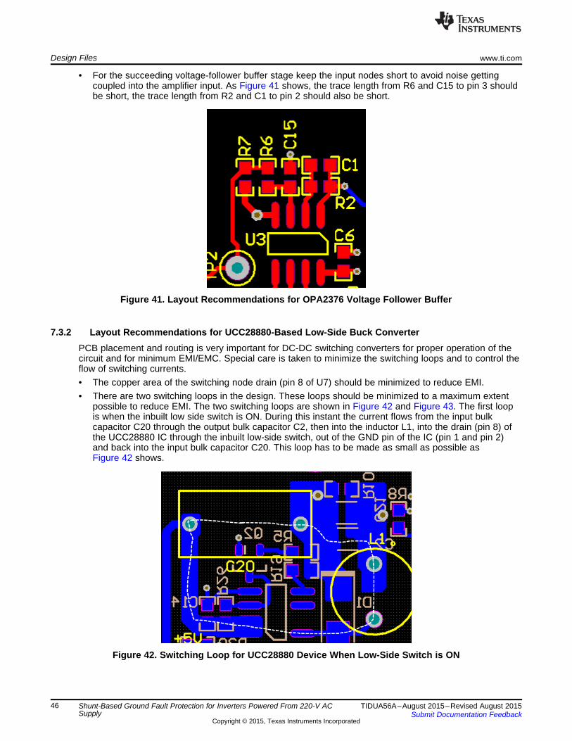
Design Files www.ti.com
• For the succeeding voltage-follower buffer stage keep the input nodes short to avoid noise gettingcoupled into the amplifier input. As Figure 41 shows, the trace length from R6 and C15 to pin 3 shouldbe short, the trace length from R2 and C1 to pin 2 should also be short.
Figure 41. Layout Recommendations for OPA2376 Voltage Follower Buffer
7.3.2 Layout Recommendations for UCC28880-Based Low-Side Buck ConverterPCB placement and routing is very important for DC-DC switching converters for proper operation of thecircuit and for minimum EMI/EMC. Special care is taken to minimize the switching loops and to control theflow of switching currents.• The copper area of the switching node drain (pin 8 of U7) should be minimized to reduce EMI.• There are two switching loops in the design. These loops should be minimized to a maximum extent
possible to reduce EMI. The two switching loops are shown in Figure 42 and Figure 43. The first loopis when the inbuilt low side switch is ON. During this instant the current flows from the input bulkcapacitor C20 through the output bulk capacitor C2, then into the inductor L1, into the drain (pin 8) ofthe UCC28880 IC through the inbuilt low-side switch, out of the GND pin of the IC (pin 1 and pin 2)and back into the input bulk capacitor C20. This loop has to be made as small as possible asFigure 42 shows.
Figure 42. Switching Loop for UCC28880 Device When Low-Side Switch is ON
46 Shunt-Based Ground Fault Protection for Inverters Powered From 220-V AC TIDUA56A–August 2015–Revised August 2015Supply Submit Documentation Feedback
Copyright © 2015, Texas Instruments Incorporated

www.ti.com Design Files
• Figure 43 shows the second switching loop. This switching loop happens when the inbuilt low sideswitch is OFF. Current flows through the output bulk capacitor C2, through the inductor L1 and backinto the capacitor C2 through freewheeling diode D1. This loop has been minimized as much aspossible in the layout.
Figure 43. Switching Loop for UCC28880 Device When Low-Side Switch is OFF
• The floating output supply must be taken out from the output bulk capacitor C2 terminals.• The feedback section consists of R26, Q2m and R5. The resistor R26 must be kept close to feedback
pin of the IC.• The decoupling capacitor C14 should be kept close to the power pin of the IC• A star connection has to be done from the DC-DC converter GND to the main GND of the PCB as
Figure 44 shows. This is done to ensure that none of the switching current passes through the mainGND of the PCB thus avoiding GND noise issues.
Figure 44. Star Connection to PCB Main GND
47TIDUA56A–August 2015–Revised August 2015 Shunt-Based Ground Fault Protection for Inverters Powered From 220-V ACSupplySubmit Documentation Feedback
Copyright © 2015, Texas Instruments Incorporated

Design Files www.ti.com
7.3.3 Layout Recommendations for Low-Side Current MonitorFigure 45 shows the layout for the low-side current sense circuit. Be sure to utilize the following steps forthis layout:• Use Kelvin connections from the low-side current shunt resistor. Place the difference amplifier close to
the shunt resistor and join it with short balanced traces to avoid offset voltages created due to inputbias current of the op-amp and the trace parasitics.
• Keep all traces at the inverting and non-inverting nodes of the op-amp to be very short. Any noisecoupled into these pins will be amplified and appear on the output.
• Place the power supply noise decoupling capacitor C6 very close to the power supply pin of the IC.The function of this capacitor is to decouple the noise from the rest of the circuit from entering the IC.Therefore during layout care should be taken that the power supply first enters the capacitor and theninto the IC power pin, if this is not done the decoupling capacitor does not decouple the noiseeffectively. Also trace length from the decoupling capacitor to the IC power pin should be kept veryshort to minimize the trace stray parasitic inductance.
Figure 45. Layout Recommendations for Low-Side Current Sense Circuit
48 Shunt-Based Ground Fault Protection for Inverters Powered From 220-V AC TIDUA56A–August 2015–Revised August 2015Supply Submit Documentation Feedback
Copyright © 2015, Texas Instruments Incorporated

LoadSource
High current pathRshunt
+ -Differential amplifier
Load
High current path
Rps Rps
Rshunt
+ -Differential amplifier
Source
www.ti.com Design Files
7.3.4 Low-Side and High-Side Sense Resistor Wiring (Kelvin Connections)Figure 46 shows the layout for the low-side current sense circuit. Be sure to utilize the following steps forthis layout:• Current can be most precisely measured with the help of current shunt resistors. To make the power
dissipation in these resistors negligible, very small values of current shunt resistors are used which areusually in the range of mΩ. At this range of resistance values the contact resistance and thetermination resistance may be larger than the value of the resistor itself or may be a significantpercentage in comparison to the value of the resistor. Therefore, if the voltage drop is measuredacross the resistor terminals, such as in Figure 46, the user is actually measuring the sum of thevoltage drops across the resistor and the resistor contacts as well as a part of the high current carryingtrace. This adds a significant error to the actual voltage drop across the resistor that the user intends tomeasure.
• This error can be avoided by using Kelvin sense connections Figure 46 shows. Now the senseconnection is isolated from the actual current carrying path. The voltage drop measured is the actualvoltage drop across the resistor.
• For very low values of shunt resistors, a four-terminal resistor along with a Kelvin connection must beused to obtain good accuracy.
Figure 46. Non-Kelvin Connection Versus Kelvin Connection
49TIDUA56A–August 2015–Revised August 2015 Shunt-Based Ground Fault Protection for Inverters Powered From 220-V ACSupplySubmit Documentation Feedback
Copyright © 2015, Texas Instruments Incorporated
Design Files www.ti.com
7.3.5 Layout PrintsThe size of the PCB is 71.12 mm × 62.23 mm. To download the layout prints for each board, see thedesign files at TIDA-00442.
7.4 Altium ProjectTo download the Altium project files for each board, see the design files at TIDA-00442.
7.5 Gerber FilesTo download the Gerber files for each board, see the design files at TIDA-00442.
7.6 Assembly DrawingsTo download the assembly drawings for each board, see the design files at TIDA-00442.
8 References
1. Texas Instruments, High Voltage 1 2 V – 400 V DC Current Sense Reference Design,Verified Design Guide (TIDU833)
2. Texas Instruments, Using the UCC28880EVM-615, UCC28880EVM-615 User's Guide (SLUUB57)3. Texas Instruments, High Voltage Digital Motor Control Kit (R1.1) Quick Start Guide,
(http://bit.ly/1J4rhaI)4. Texas Instruments, HVMotorCtrl + PFC (R1.1) Kit How t o Run Guide, (http://bit.ly/1TVVSu5)5. EETimes, A Current Sensing Tutorial—Part IV: Layout and Troubleshooting Guidelines,
Design How-To (http://ubm.io/1LjBSiY)
9 About the AuthorPAWAN NAYAK is a Systems Engineer at Texas Instruments where he is responsible for developingreference design solutions for the Motor Drive segment within Industrial Systems. Pawan brings to thisrole his experience in analog system design, mixed signal design and power supplies. Pawan earned hisBachelor of Engineering in Electronics and Communication Engineering from Visvesvaraya TechnologicalUniversity, India.
N. NAVANEETH KUMAR is a Systems Architect at Texas Instruments, where he is responsible fordeveloping subsystem solutions for motor controls within Industrial Systems. N. Navaneeth brings to thisrole his extensive experience in power electronics, EMC, Analog, and mixed signal designs. He hassystem-level product design experience in drives, solar inverters, UPS, and protection relays. N.Navaneeth earned his Bachelor of Electronics and Communication Engineering from BharathiarUniversity, India and his Master of Science in Electronic Product Development from Bolton University, UK.
50 Shunt-Based Ground Fault Protection for Inverters Powered From 220-V AC TIDUA56A–August 2015–Revised August 2015Supply Submit Documentation Feedback
Copyright © 2015, Texas Instruments Incorporated

IMPORTANT NOTICE FOR TI REFERENCE DESIGNS
Texas Instruments Incorporated ("TI") reference designs are solely intended to assist designers (“Buyers”) who are developing systems thatincorporate TI semiconductor products (also referred to herein as “components”). Buyer understands and agrees that Buyer remainsresponsible for using its independent analysis, evaluation and judgment in designing Buyer’s systems and products.TI reference designs have been created using standard laboratory conditions and engineering practices. TI has not conducted anytesting other than that specifically described in the published documentation for a particular reference design. TI may makecorrections, enhancements, improvements and other changes to its reference designs.Buyers are authorized to use TI reference designs with the TI component(s) identified in each particular reference design and to modify thereference design in the development of their end products. HOWEVER, NO OTHER LICENSE, EXPRESS OR IMPLIED, BY ESTOPPELOR OTHERWISE TO ANY OTHER TI INTELLECTUAL PROPERTY RIGHT, AND NO LICENSE TO ANY THIRD PARTY TECHNOLOGYOR INTELLECTUAL PROPERTY RIGHT, IS GRANTED HEREIN, including but not limited to any patent right, copyright, mask work right,or other intellectual property right relating to any combination, machine, or process in which TI components or services are used.Information published by TI regarding third-party products or services does not constitute a license to use such products or services, or awarranty or endorsement thereof. Use of such information may require a license from a third party under the patents or other intellectualproperty of the third party, or a license from TI under the patents or other intellectual property of TI.TI REFERENCE DESIGNS ARE PROVIDED "AS IS". TI MAKES NO WARRANTIES OR REPRESENTATIONS WITH REGARD TO THEREFERENCE DESIGNS OR USE OF THE REFERENCE DESIGNS, EXPRESS, IMPLIED OR STATUTORY, INCLUDING ACCURACY ORCOMPLETENESS. TI DISCLAIMS ANY WARRANTY OF TITLE AND ANY IMPLIED WARRANTIES OF MERCHANTABILITY, FITNESSFOR A PARTICULAR PURPOSE, QUIET ENJOYMENT, QUIET POSSESSION, AND NON-INFRINGEMENT OF ANY THIRD PARTYINTELLECTUAL PROPERTY RIGHTS WITH REGARD TO TI REFERENCE DESIGNS OR USE THEREOF. TI SHALL NOT BE LIABLEFOR AND SHALL NOT DEFEND OR INDEMNIFY BUYERS AGAINST ANY THIRD PARTY INFRINGEMENT CLAIM THAT RELATES TOOR IS BASED ON A COMBINATION OF COMPONENTS PROVIDED IN A TI REFERENCE DESIGN. IN NO EVENT SHALL TI BELIABLE FOR ANY ACTUAL, SPECIAL, INCIDENTAL, CONSEQUENTIAL OR INDIRECT DAMAGES, HOWEVER CAUSED, ON ANYTHEORY OF LIABILITY AND WHETHER OR NOT TI HAS BEEN ADVISED OF THE POSSIBILITY OF SUCH DAMAGES, ARISING INANY WAY OUT OF TI REFERENCE DESIGNS OR BUYER’S USE OF TI REFERENCE DESIGNS.TI reserves the right to make corrections, enhancements, improvements and other changes to its semiconductor products and services perJESD46, latest issue, and to discontinue any product or service per JESD48, latest issue. Buyers should obtain the latest relevantinformation before placing orders and should verify that such information is current and complete. All semiconductor products are soldsubject to TI’s terms and conditions of sale supplied at the time of order acknowledgment.TI warrants performance of its components to the specifications applicable at the time of sale, in accordance with the warranty in TI’s termsand conditions of sale of semiconductor products. Testing and other quality control techniques for TI components are used to the extent TIdeems necessary to support this warranty. Except where mandated by applicable law, testing of all parameters of each component is notnecessarily performed.TI assumes no liability for applications assistance or the design of Buyers’ products. Buyers are responsible for their products andapplications using TI components. To minimize the risks associated with Buyers’ products and applications, Buyers should provideadequate design and operating safeguards.Reproduction of significant portions of TI information in TI data books, data sheets or reference designs is permissible only if reproduction iswithout alteration and is accompanied by all associated warranties, conditions, limitations, and notices. TI is not responsible or liable forsuch altered documentation. Information of third parties may be subject to additional restrictions.Buyer acknowledges and agrees that it is solely responsible for compliance with all legal, regulatory and safety-related requirementsconcerning its products, and any use of TI components in its applications, notwithstanding any applications-related information or supportthat may be provided by TI. Buyer represents and agrees that it has all the necessary expertise to create and implement safeguards thatanticipate dangerous failures, monitor failures and their consequences, lessen the likelihood of dangerous failures and take appropriateremedial actions. Buyer will fully indemnify TI and its representatives against any damages arising out of the use of any TI components inBuyer’s safety-critical applications.In some cases, TI components may be promoted specifically to facilitate safety-related applications. With such components, TI’s goal is tohelp enable customers to design and create their own end-product solutions that meet applicable functional safety standards andrequirements. Nonetheless, such components are subject to these terms.No TI components are authorized for use in FDA Class III (or similar life-critical medical equipment) unless authorized officers of the partieshave executed an agreement specifically governing such use.Only those TI components that TI has specifically designated as military grade or “enhanced plastic” are designed and intended for use inmilitary/aerospace applications or environments. Buyer acknowledges and agrees that any military or aerospace use of TI components thathave not been so designated is solely at Buyer's risk, and Buyer is solely responsible for compliance with all legal and regulatoryrequirements in connection with such use.TI has specifically designated certain components as meeting ISO/TS16949 requirements, mainly for automotive use. In any case of use ofnon-designated products, TI will not be responsible for any failure to meet ISO/TS16949.IMPORTANT NOTICE
Mailing Address: Texas Instruments, Post Office Box 655303, Dallas, Texas 75265Copyright © 2015, Texas Instruments Incorporated


![N. Vedachalam Journal Ocean Engineering Science · switching operations, and fault limiting and interrupting de- vices [13]. Bulk power conversion systems require multiple inverters](https://img.pdfslide.net/doc/110x75/5f04c2837e708231d40f90dc/n-vedachalam-journal-ocean-engineering-science-switching-operations-and-fault.jpg)