Embed Size (px)
Citation preview

Spartan-6 FPGA Power Management
User Guide
UG394 (v1.3) January 21, 2016
Spartan-6 FPGA Power Management www.xilinx.com UG394 (v1.3) January 21, 2016
Notice of DisclaimerThe information disclosed to you hereunder (the “Materials”) is provided solely for the selection and use of Xilinx products. To the maximum extent permitted by applicable law: (1) Materials are made available "AS IS" and with all faults, Xilinx hereby DISCLAIMS ALL WARRANTIES AND CONDITIONS, EXPRESS, IMPLIED, OR STATUTORY, INCLUDING BUT NOT LIMITED TO WARRANTIES OF MERCHANTABILITY, NON-INFRINGEMENT, OR FITNESS FOR ANY PARTICULAR PURPOSE; and (2) Xilinx shall not be liable (whether in contract or tort, including negligence, or under any other theory of liability) for any loss or damage of any kind or nature related to, arising under, or in connection with, the Materials (including your use of the Materials), including for any direct, indirect, special, incidental, or consequential loss or damage (including loss of data, profits, goodwill, or any type of loss or damage suffered as a result of any action brought by a third party) even if such damage or loss was reasonably foreseeable or Xilinx had been advised of the possibility of the same. Xilinx assumes no obligation to correct any errors contained in the Materials or to notify you of updates to the Materials or to product specifications. You may not reproduce, modify, distribute, or publicly display the Materials without prior written consent. Certain products are subject to the terms and conditions of Xilinx’s limited warranty, please refer to Xilinx’s Terms of Sale which can be viewed at www.xilinx.com/legal.htm#tos; IP cores may be subject to warranty and support terms contained in a license issued to you by Xilinx. Xilinx products are not designed or intended to be fail-safe or for use in any application requiring fail-safe performance; you assume sole risk and liability for use of Xilinx products in such critical applications, please refer to Xilinx’s Terms of Sale which can be viewed at www.xilinx.com/legal.htm#tos.© Copyright 2010–2016 Xilinx, Inc. Xilinx, the Xilinx logo, Artix, ISE, Kintex, Spartan, Virtex, Vivado, Zynq, and other designated brands included herein are trademarks of Xilinx in the United States and other countries. All other trademarks are the property of their respective owners.
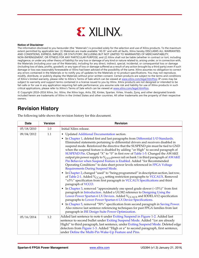
Revision HistoryThe following table shows the revision history for this document.
Date Version Revision
05/18/2010 1.0 Initial Xilinx release.
09/04/2012 1.1 • Updated Additional Documentation section.• In Chapter 1, deleted first and last paragraphs from Differential I/O Standards.
Eliminated statements pertaining to differential drivers and receivers disabled in suspend mode. Reinforced the directive that the SUSPEND pin must be tied to GND when the suspend feature is disabled by adding “or High” to second paragraph of SUSPEND Pin. Changed “X” to “0” in first row of Table 1-5. Changed the AWAKE output pin power supply to VCCO power rail on bank 1 in third paragraph of AWAKE Pin Behavior when Suspend Feature is Enabled. Added “for Recommended Operating Conditions” to data sheet power levels referenced in FPGA Voltage Requirements During Suspend Mode.
• In Chapter 2, changed “used” to “being programmed” in description section, last row, of Table 2-1. Added VCCAUX setting restriction paragraphs to VCCAUX. Removed “±5%” specification from first paragraph in VCCAUX Specifications and third paragraph of VCCO.
• In Chapter 3, removed “approximately one speed grade slower (~15%)” from first paragraph in Introduction. Added a UG382 reference to Designing Using the Lower-Power Spartan-6 LX Devices. Added VCCAUX and IODELAY2 specification paragraphs to Lower-Power Spartan-6 LX Device Specifications.
• In Chapter 5, removed “50%” specification from second paragraph in Saving Power. Also remove last sentence referencing techniques for past FPGA families from last paragraph in ISE Design Suite Power Optimization.
05/16/2014 1.2 Added last sentence to note 6 under Exiting Suspend in Figure 1-2. Added last sentence to second bullet under Exiting Suspend Mode. Added “(or are already High)” to third paragraph, last sentence, under Exiting Suspend Mode. Deleted edge detectors from Figure 1-3. Added “High or a“ to second paragraph, first sentence, under Define the Multi-Pin Wake-Up Feature and Pins.
UG394 (v1.3) January 21, 2016 www.xilinx.com Spartan-6 FPGA Power Management
01/21/2016 1.3 Clarified the last sentence under PROGRAM_B Programming Pin Always Overrides Suspend Mode in Chapter 1.
Date Version Revision
Spartan-6 FPGA Power Management www.xilinx.com 5UG394 (v1.3) January 21, 2016
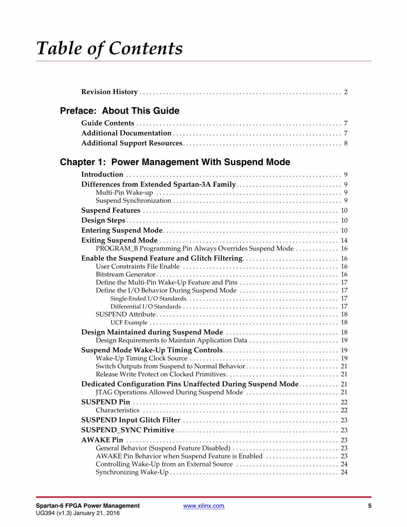
Revision History . . . . . . . . . . . . . . . . . . . . . . . . . . . . . . . . . . . . . . . . . . . . . . . . . . . . . . . . . . . . . 2
Preface: About This GuideGuide Contents . . . . . . . . . . . . . . . . . . . . . . . . . . . . . . . . . . . . . . . . . . . . . . . . . . . . . . . . . . . . . . 7Additional Documentation . . . . . . . . . . . . . . . . . . . . . . . . . . . . . . . . . . . . . . . . . . . . . . . . . . . 7Additional Support Resources . . . . . . . . . . . . . . . . . . . . . . . . . . . . . . . . . . . . . . . . . . . . . . . . 8
Chapter 1: Power Management With Suspend ModeIntroduction . . . . . . . . . . . . . . . . . . . . . . . . . . . . . . . . . . . . . . . . . . . . . . . . . . . . . . . . . . . . . . . . . 9Differences from Extended Spartan-3A Family. . . . . . . . . . . . . . . . . . . . . . . . . . . . . . . . 9
Multi-Pin Wake-up . . . . . . . . . . . . . . . . . . . . . . . . . . . . . . . . . . . . . . . . . . . . . . . . . . . . . . . . 9Suspend Synchronization . . . . . . . . . . . . . . . . . . . . . . . . . . . . . . . . . . . . . . . . . . . . . . . . . . . 9
Suspend Features . . . . . . . . . . . . . . . . . . . . . . . . . . . . . . . . . . . . . . . . . . . . . . . . . . . . . . . . . . . 10Design Steps . . . . . . . . . . . . . . . . . . . . . . . . . . . . . . . . . . . . . . . . . . . . . . . . . . . . . . . . . . . . . . . . 10Entering Suspend Mode . . . . . . . . . . . . . . . . . . . . . . . . . . . . . . . . . . . . . . . . . . . . . . . . . . . . . 10Exiting Suspend Mode . . . . . . . . . . . . . . . . . . . . . . . . . . . . . . . . . . . . . . . . . . . . . . . . . . . . . . 14
PROGRAM_B Programming Pin Always Overrides Suspend Mode . . . . . . . . . . . . . 16Enable the Suspend Feature and Glitch Filtering. . . . . . . . . . . . . . . . . . . . . . . . . . . . . 16
User Constraints File Enable . . . . . . . . . . . . . . . . . . . . . . . . . . . . . . . . . . . . . . . . . . . . . . . 16Bitstream Generator . . . . . . . . . . . . . . . . . . . . . . . . . . . . . . . . . . . . . . . . . . . . . . . . . . . . . . . 16Define the Multi-Pin Wake-Up Feature and Pins . . . . . . . . . . . . . . . . . . . . . . . . . . . . . . 17Define the I/O Behavior During Suspend Mode . . . . . . . . . . . . . . . . . . . . . . . . . . . . . . 17
Single-Ended I/O Standards. . . . . . . . . . . . . . . . . . . . . . . . . . . . . . . . . . . . . . . . . . . . . . 17Differential I/O Standards . . . . . . . . . . . . . . . . . . . . . . . . . . . . . . . . . . . . . . . . . . . . . . . 17
SUSPEND Attribute . . . . . . . . . . . . . . . . . . . . . . . . . . . . . . . . . . . . . . . . . . . . . . . . . . . . . . . 18UCF Example . . . . . . . . . . . . . . . . . . . . . . . . . . . . . . . . . . . . . . . . . . . . . . . . . . . . . . . . . 18
Design Maintained during Suspend Mode . . . . . . . . . . . . . . . . . . . . . . . . . . . . . . . . . . 18Design Requirements to Maintain Application Data . . . . . . . . . . . . . . . . . . . . . . . . . . . 19
Suspend Mode Wake-Up Timing Controls. . . . . . . . . . . . . . . . . . . . . . . . . . . . . . . . . . . 19Wake-Up Timing Clock Source . . . . . . . . . . . . . . . . . . . . . . . . . . . . . . . . . . . . . . . . . . . . . 19Switch Outputs from Suspend to Normal Behavior . . . . . . . . . . . . . . . . . . . . . . . . . . . . 21Release Write Protect on Clocked Primitives. . . . . . . . . . . . . . . . . . . . . . . . . . . . . . . . . . 21
Dedicated Configuration Pins Unaffected During Suspend Mode . . . . . . . . . . . . 21JTAG Operations Allowed During Suspend Mode . . . . . . . . . . . . . . . . . . . . . . . . . . . . 21
SUSPEND Pin . . . . . . . . . . . . . . . . . . . . . . . . . . . . . . . . . . . . . . . . . . . . . . . . . . . . . . . . . . . . . . 22Characteristics . . . . . . . . . . . . . . . . . . . . . . . . . . . . . . . . . . . . . . . . . . . . . . . . . . . . . . . . . . . 22
SUSPEND Input Glitch Filter . . . . . . . . . . . . . . . . . . . . . . . . . . . . . . . . . . . . . . . . . . . . . . . 23SUSPEND_SYNC Primitive . . . . . . . . . . . . . . . . . . . . . . . . . . . . . . . . . . . . . . . . . . . . . . . . . 23AWAKE Pin . . . . . . . . . . . . . . . . . . . . . . . . . . . . . . . . . . . . . . . . . . . . . . . . . . . . . . . . . . . . . . . . 23
General Behavior (Suspend Feature Disabled) . . . . . . . . . . . . . . . . . . . . . . . . . . . . . . . . 23AWAKE Pin Behavior when Suspend Feature is Enabled . . . . . . . . . . . . . . . . . . . . . . 23Controlling Wake-Up from an External Source . . . . . . . . . . . . . . . . . . . . . . . . . . . . . . . 24Synchronizing Wake-Up . . . . . . . . . . . . . . . . . . . . . . . . . . . . . . . . . . . . . . . . . . . . . . . . . . . 24
Table of Contents
6 www.xilinx.com Spartan-6 FPGA Power ManagementUG394 (v1.3) January 21, 2016
Post-Configuration CRC Limitations When Using Suspend Mode. . . . . . . . . . . . 24FPGA Voltage Requirements During Suspend Mode . . . . . . . . . . . . . . . . . . . . . . . . 26Memory Controller Block . . . . . . . . . . . . . . . . . . . . . . . . . . . . . . . . . . . . . . . . . . . . . . . . . . . 26
Chapter 2: Voltage SuppliesIntroduction . . . . . . . . . . . . . . . . . . . . . . . . . . . . . . . . . . . . . . . . . . . . . . . . . . . . . . . . . . . . . . . . 27VCCINT . . . . . . . . . . . . . . . . . . . . . . . . . . . . . . . . . . . . . . . . . . . . . . . . . . . . . . . . . . . . . . . . . . . . 28VCCAUX . . . . . . . . . . . . . . . . . . . . . . . . . . . . . . . . . . . . . . . . . . . . . . . . . . . . . . . . . . . . . . . . . . . 28
Setting the VCCAUX Level . . . . . . . . . . . . . . . . . . . . . . . . . . . . . . . . . . . . . . . . . . . . . . . . 29VCCAUX Specifications . . . . . . . . . . . . . . . . . . . . . . . . . . . . . . . . . . . . . . . . . . . . . . . . . . . 29
VCCO . . . . . . . . . . . . . . . . . . . . . . . . . . . . . . . . . . . . . . . . . . . . . . . . . . . . . . . . . . . . . . . . . . . . . . 29VREF . . . . . . . . . . . . . . . . . . . . . . . . . . . . . . . . . . . . . . . . . . . . . . . . . . . . . . . . . . . . . . . . . . . . . . . 30Board Design and Signal Integrity. . . . . . . . . . . . . . . . . . . . . . . . . . . . . . . . . . . . . . . . . . . 30
Simultaneously Switching Outputs. . . . . . . . . . . . . . . . . . . . . . . . . . . . . . . . . . . . . . . . . . 30Power Distribution System Design and Decoupling/Bypass Capacitors . . . . . . . . . . 30
Chapter 3: Lower-Power Spartan-6 LX DevicesIntroduction . . . . . . . . . . . . . . . . . . . . . . . . . . . . . . . . . . . . . . . . . . . . . . . . . . . . . . . . . . . . . . . . 31Designing Using the Lower-Power Spartan-6 LX Devices . . . . . . . . . . . . . . . . . . . . 31Lower-Power Spartan-6 LX Device Specifications . . . . . . . . . . . . . . . . . . . . . . . . . . . . 32
Chapter 4: Power-On and Power-Down Behavior Including HibernateIntroduction . . . . . . . . . . . . . . . . . . . . . . . . . . . . . . . . . . . . . . . . . . . . . . . . . . . . . . . . . . . . . . . . 33Power-On Reset . . . . . . . . . . . . . . . . . . . . . . . . . . . . . . . . . . . . . . . . . . . . . . . . . . . . . . . . . . . . . 33Supply Sequencing . . . . . . . . . . . . . . . . . . . . . . . . . . . . . . . . . . . . . . . . . . . . . . . . . . . . . . . . . 34Ramp Rate . . . . . . . . . . . . . . . . . . . . . . . . . . . . . . . . . . . . . . . . . . . . . . . . . . . . . . . . . . . . . . . . . . 34Hot Swap . . . . . . . . . . . . . . . . . . . . . . . . . . . . . . . . . . . . . . . . . . . . . . . . . . . . . . . . . . . . . . . . . . . 34Configuration Data Retention and Brown Out . . . . . . . . . . . . . . . . . . . . . . . . . . . . . . . 35GTP Transceiver Power-Up and Power-Down . . . . . . . . . . . . . . . . . . . . . . . . . . . . . . . 35Hibernate Power Down . . . . . . . . . . . . . . . . . . . . . . . . . . . . . . . . . . . . . . . . . . . . . . . . . . . . . 35
Forcing FPGA to Quiescent Current Levels . . . . . . . . . . . . . . . . . . . . . . . . . . . . . . . . . . . 36Entering Hibernate State . . . . . . . . . . . . . . . . . . . . . . . . . . . . . . . . . . . . . . . . . . . . . . . . . . . 36Turn Off VCCO . . . . . . . . . . . . . . . . . . . . . . . . . . . . . . . . . . . . . . . . . . . . . . . . . . . . . . . . . . 37Exiting Hibernate . . . . . . . . . . . . . . . . . . . . . . . . . . . . . . . . . . . . . . . . . . . . . . . . . . . . . . . . . 38Design Considerations . . . . . . . . . . . . . . . . . . . . . . . . . . . . . . . . . . . . . . . . . . . . . . . . . . . . 38
Chapter 5: Power EstimationIntroduction . . . . . . . . . . . . . . . . . . . . . . . . . . . . . . . . . . . . . . . . . . . . . . . . . . . . . . . . . . . . . . . . 39Voltage Regulators . . . . . . . . . . . . . . . . . . . . . . . . . . . . . . . . . . . . . . . . . . . . . . . . . . . . . . . . . . 39Saving Power . . . . . . . . . . . . . . . . . . . . . . . . . . . . . . . . . . . . . . . . . . . . . . . . . . . . . . . . . . . . . . . 40
Saving Clock Routing Power . . . . . . . . . . . . . . . . . . . . . . . . . . . . . . . . . . . . . . . . . . . . . . . 41ISE Design Suite Power Optimization . . . . . . . . . . . . . . . . . . . . . . . . . . . . . . . . . . . . . . . 41
Spartan-6 FPGA Power Management www.xilinx.com 7UG394 (v1.3) January 21, 2016
Preface
About This Guide
This document provides information on the various hardware methods of power management in Spartan-6 FPGAs, primarily focusing on the suspend mode. Other power management topics include the lower-power Spartan-6 LX devices (-1L) and the programmable VCCAUX level available in all Spartan-6 devices. In addition, more detail is provided on the power rails, including hot swap and hibernate (power-off) options.
Guide ContentsThis user guide contains the following chapters:
• Chapter 1, Power Management With Suspend Mode
• Chapter 2, Voltage Supplies
• Chapter 3, Lower-Power Spartan-6 LX Devices
• Chapter 4, Power-On and Power-Down Behavior Including Hibernate
• Chapter 5, Power Estimation
Additional DocumentationThese documents are available for download at http://www.xilinx.com/support/documentation/spartan-6.htm.
• Spartan-6 Family Overview
This overview outlines the features and product selection of the Spartan-6 family.
• Spartan-6 FPGA Data Sheet: DC and Switching Characteristics
This data sheet contains the DC and switching characteristic specifications for the Spartan-6 family.
• Spartan-6 FPGA Packaging and Pinout Specifications
This specification includes the tables for device/package combinations and maximum I/Os, pin definitions, pinout tables, pinout diagrams, mechanical drawings, and thermal specifications.
• Spartan-6 FPGA Configuration User Guide
This all-encompassing configuration guide includes chapters on configuration interfaces (serial and parallel), multi-bitstream management, bitstream encryption, boundary-scan and JTAG configuration, and reconfiguration techniques.
• Spartan-6 FPGA SelectIO Resources User Guide
This guide describes the SelectIO™ resources available in all Spartan-6 devices.
8 www.xilinx.com Spartan-6 FPGA Power ManagementUG394 (v1.3) January 21, 2016
Running H/F 3
• Spartan-6 FPGA Clocking Resources User Guide
This guide describes the clocking resources available in all Spartan-6 devices, including the DCMs and PLLs.
• Spartan-6 FPGA Block RAM Resources User Guide
This guide describes the Spartan-6 device block RAM capabilities.
• Spartan-6 FPGA Configurable Logic Blocks User Guide
This guide describes the capabilities of the configurable logic blocks (CLBs) available in all Spartan-6 devices.
• Spartan-6 FPGA GTP Transceivers User Guide
This guide describes the GTP transceivers available in the Spartan-6 LXT FPGAs.
• Spartan-6 FPGA DSP48A1 Slice User Guide
This guide describes the architecture of the DSP48A1 slice in Spartan-6 FPGAs and provides configuration examples.
• Spartan-6 FPGA Memory Controller User Guide
This guide describes the Spartan-6 FPGA memory controller block, a dedicated embedded multi-port memory controller that greatly simplifies interfacing Spartan-6 FPGAs to the most popular memory standards.
• Spartan-6 FPGA PCB Design and Pin Planning Guide
This guide provides information on PCB design for Spartan-6 devices, with a focus on strategies for making design decisions at the PCB and interface level.
These documents provide additional background:
• WP298, Power Consumption at 40 nm and 45 nm, White Paper
At 40 and 45 nm process nodes, power has become the primary factor for FPGA selection. Spartan-6 FPGAs offer lower power, simpler power systems and PCB complexity, better reliability, and lower system cost. This white paper details how Xilinx designed for this new reality in Spartan-6 (45 nm) and Virtex®-6 (40 nm) FPGA families, achieving dramatic power reductions over previous generation devices.
• WP370, Reducing Switching Power with Intelligent Clock Gating, White Paper
Xilinx delivers the first automated, fine-grain clock-gating solution that can reduce dynamic power by up to 30% for Spartan-6 FPGA designs.
• WP396, High-Volume Spartan-6 FPGAs: Performance and Power Leadership by Design, White Paper
This white paper describes how Spartan-6 FPGAs address the needs of high-volume systems. The ability to connect efficiently and inexpensively to commodity memories, high-performance chip-to-chip interface capability, and innovative power down modes are just a few of the problems solved by high-performance, low-power, and low-cost Spartan-6 FPGAs.
Additional Support ResourcesTo search the database of silicon and software questions and answers or to create a technical support case in WebCase, see the Xilinx website at:
http://www.xilinx.com/support.
Spartan-6 FPGA Power Management www.xilinx.com 9UG394 (v1.3) January 21, 2016
Chapter 1
Power Management With Suspend Mode
IntroductionSome applications require the lowest possible system cost or highest performance, and other applications require the lowest possible standby power. Spartan®-6 FPGAs offer low-power options to balance these cost and performance trade-offs.
The Spartan-6 family offers the suspend mode, an advanced static power-management feature, which reduces FPGA power consumption while retaining the FPGA's configuration data and maintaining the design. The device can quickly enter and exit suspend mode as required in an application.
Differences from Extended Spartan-3A FamilyThe suspend mode in Spartan-6 FPGAs is a superset of the suspend feature in the Extended Spartan-3A FPGAs. Two new enhancements include multi-pin wake-up and suspend synchronization.
Multi-Pin Wake-upThe multi-pin wake-up feature allows the FPGA to monitor for a wake-up signal on up to eight pins. In the Extended Spartan-3A family, monitoring was limited to the SUSPEND pin itself. Multi-pin wake-up also allows a number of independent sources to trigger the FPGA to return to the normal application.
Suspend SynchronizationThe Spartan-6 FPGA primitive, SUSPEND_SYNC, enables the synchronization of the suspend action with the application design. In the Extended Spartan-3A family, the suspend mode activation begins immediately upon asserting the SUSPEND pin. The Spartan-6 FPGA SUSPEND_SYNC primitive allows the application design to acknowledge a suspend request, thereby allowing the application to finish necessary functions prior to entering the suspend mode.
10 www.xilinx.com Spartan-6 FPGA Power ManagementUG394 (v1.3) January 21, 2016
Chapter 1: Power Management With Suspend Mode
Suspend FeaturesThe significant features and benefits of the suspend mode:
• Quickly and easily puts the FPGA into a static condition, eliminating most active current.
• Reduces quiescent current by 40% or more.
• Retains FPGA configuration data and the state of the FPGA application during suspend mode.
• Fast, programmable FPGA wake-up time from suspend mode.
• Individual control on each user-I/O pin to define pin behavior while in suspend mode.
• Activated externally by the system using a single dedicated control pin (SUSPEND).
• Indicates the present suspend mode status using the AWAKE pin.
• Awakens an FPGA in suspend mode using any of eight SUSPEND control pins (SCP).
• SUSPEND_SYNC primitive to acknowledge a ready state prior to entering suspend mode.
Design StepsTo use the suspend feature:
• Enable the Suspend Feature and Glitch Filtering, page 16
• Define the Multi-Pin Wake-Up Feature and Pins, page 17
• Define the I/O Behavior During Suspend Mode, page 17
• Implement steps to maintain application data during suspend mode (SUSPEND_SYNC) (see Design Requirements to Maintain Application Data, page 19)
• Define the Suspend Mode Wake-Up Timing Controls, page 19
• Define the AWAKE Pin Behavior when Suspend Feature is Enabled, page 23
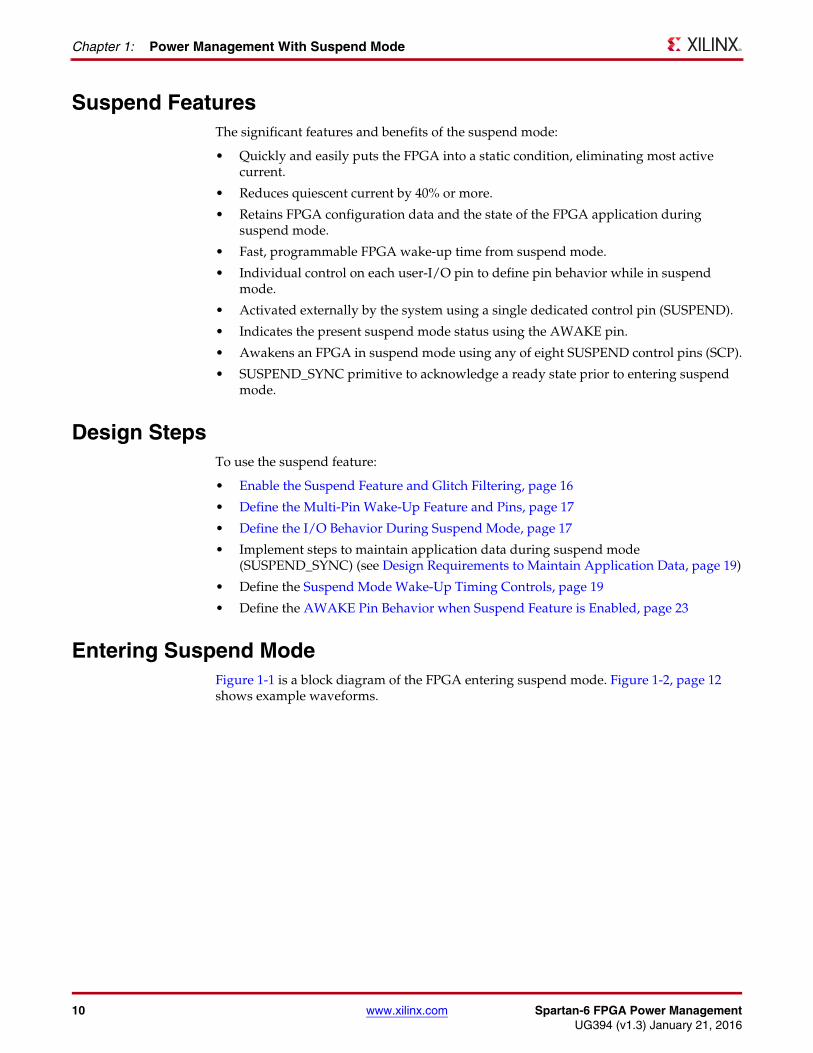
Entering Suspend ModeFigure 1-1 is a block diagram of the FPGA entering suspend mode. Figure 1-2, page 12 shows example waveforms.
Spartan-6 FPGA Power Management www.xilinx.com 11UG394 (v1.3) January 21, 2016
Entering Suspend Mode
The FPGA can only enter suspend mode if enabled in the configuration bitstream (see Enable the Suspend Feature and Glitch Filtering, page 16). The SUSPEND pin must be Low during power up and configuration. Once enabled through the bitstream, and the SUSPEND_SYNC primitive is not present in the design, when the SUSPEND pin is asserted, the FPGA unconditionally and quickly enters suspend mode.
If the SUSPEND_SYNC primitive is present in the design, the FPGA does not enter suspend mode until the suspend-acknowledge signal (SACK) is asserted. After the SUSPEND pin is asserted, the SREQ port of the SUSPEND_SYNC primitive transitions High. This can be used in the design to initiate any functions that must be completed prior to the FPGA entering suspend mode. When these functions are complete, drive the SACK port High.
After the FPGA enters suspend mode, all nonessential FPGA functions are shut down to minimize power dissipation. The FPGA retains all configuration data while in suspend mode. After entering suspend mode, all writable clocked primitives are write-protected against spurious write operations, and all FPGA inputs and interconnects are shut down. This allows the design state to be held static during suspend mode. If a specific design state must be maintained, see Design Requirements to Maintain Application Data, page 19.
X-Ref Target - Figure 1-1
Figure 1-1: Entering Suspend Mode
SUSPENDAttribute
SUSPENDAttribute
Glitch Filter
Suspend Enable
SRL
LUT RAM
Flip-Flops
Latches
Block RAM
Writable Clocked Primitives
FPGA Application Logic
FPGAInputs
FPGAOutputs
SUSPEND AWAKE
ENABLE_SUSPENDENABLE_SUSPEND
Filter Select
Write-Protect WritableClocked Primitives
Apply SUSPEND Attributeto FPGA Outputs
Block FPGAInputs
SUSPEND_SYNC
SUSPEND_SYNCInstantiated
UG394_c1_01_020310
SREQ SACK
12 www.xilinx.com Spartan-6 FPGA Power ManagementUG394 (v1.3) January 21, 2016
Chapter 1: Power Management With Suspend Mode
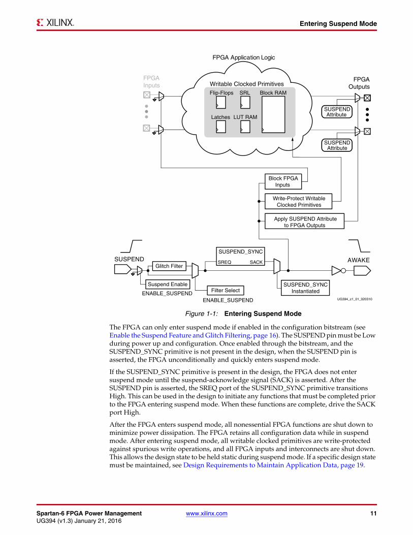
Each FPGA output pin or bidirectional I/O pin assumes its defined suspend mode behavior, which is described as part of the FPGA design using a SUSPEND attribute.
The AWAKE pin goes Low, indicating that the FPGA is in suspend mode. The DONE pin remains High while the FPGA is in suspend mode because the FPGA configuration data is not lost.
This section details the waveform notes in Figure 1-2.
Entering Suspend in Figure 1-2
1. An external signal drives the FPGA's SUSPEND pin High, unconditionally forcing the FPGA into the power-saving suspend mode (if SUSPEND_SYNC is not used). When SUSPEND_SYNC is used, this phase does not complete until the SACK port of the SUSPEND_SYNC primitive is asserted. Data values are captured for I/O pins with a SUSPEND attribute set to DRIVE_LAST_VALUE; however, this value is not presented until Step 4.
2. In response to the SUSPEND input going High or SACK assertion on the SUSPEND_SYNC primitive, and after a delay of tSUSPEND_GWE, the FPGA write protects and preserves the states of all clocked primitives. The states of all flip-flops, block RAM, distributed RAM (LUT RAM), shift registers (SRL), and I/O latches are preserved during suspend mode.
X-Ref Target - Figure 1-2
Figure 1-2: Suspend Mode Waveforms (Entering and Exiting)
ug394_c1_02_042910
Blocked
tSUSPEND_DISABLE
tAWAKE_GWE
tAWAKE_GTS
SUSPEND Input
AWAKE Output
Flip-Flops, Block RAM,Distributed RAM
FPGA Outputs
FPGA Inputs,Interconnect
Write Protected
Defined by SUSPEND Attribute
1
2
3
4
5
6
7
8
10
9
Entering Suspend Mode Exiting Suspend Mode
sw_gts_cycle
sw_gwe_cycle
tSUSPEND_ENABLE
tSUSPENDLOW_AWAKE
tSUSPEND_GTS
tSUSPENDHIGH_AWAKE
tSUSPEND_GWE
Spartan-6 FPGA Power Management www.xilinx.com 13UG394 (v1.3) January 21, 2016
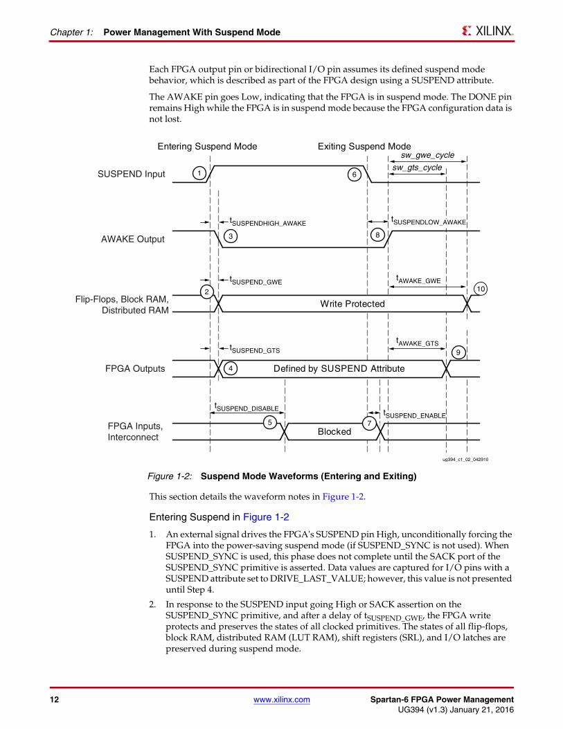
Entering Suspend Mode
3. After a delay of tSUSPENDHIGH_AWAKE, the FPGA drives the AWAKE output Low to indicate that it is entering suspend mode.
4. After a delay of tSUSPEND_GTS, the FPGA switches the normal behavior of all outputs over to the suspend mode behavior defined by the SUSPEND attribute assigned to each I/O. See Define the I/O Behavior During Suspend Mode, page 17.
5. After a delay of tSUSPEND_DISABLE, FPGA inputs are blocked and the interconnect shut off (High) to prevent any internal switching activity.
Exiting Suspend in Figure 1-2
6. The system drives the FPGA's SUSPEND input Low, causing the FPGA to exit suspend mode. If using multi-pin wake-up mode, the system first drives the FPGA's SUSPEND input LOW, then drives any of the enabled multi-pin wake-up pins High, causing the FPGA to exit suspend mode. If any of the enabled multi-pin wake-up pins are High when the SUSPEND input goes Low, the FPGA exits suspend mode immediately.
7. The FPGA releases the inputs and interconnect after a delay of tSUSPEND_ENABLE, allowing signals to propagate internally. There is no danger of corrupting the internal state because all clocked primitives are still write protected.
8. After a delay of tSUSPENDLOW_AWAKE or tSCP_AWAKE, the FPGA asserts the AWAKE signal with the bitstream option drive_awake:yes. If the option is drive_awake:no, then the FPGA releases AWAKE to become an open-drain output. In this case, an external pull-up resistor is required or an external signal must drive AWAKE High before the FPGA continues to awaken. All subsequent timing is measured from when the AWAKE output transitions High. If multiple FPGAs are waking up and need to be synchronized, set drive_awake:no in each and then use an external pull-up resistor to synchronize the AWAKE pins. If other devices are waking up and the FPGA(s) need to wait, set drive_awake:no and use an external signal to control the AWAKE pin and drive it High once the rest of the system is ready.
9. After a delay of tAWAKE_GTS, the FPGA switches output behavior from the specified SUSPEND attribute to the function specified in the FPGA application. The timing of this switch-over is controlled by the suspend/wake sw_gts_cycle bitstream generation setting, which defines when the FPGA's internal global three-state (GTS) control is released. After the specified number of clock cycles, the outputs are active according to the normal FPGA application. By default, the outputs are enabled four clock cycles after AWAKE goes High. The outputs are generally released before the clocked primitives to allow signals to propagate out of the FPGA.
10. After a delay of tAWAKE_GWE, the writable, clocked primitives are released according to the suspend/wake sw_gwe_cycle bitstream generator setting, which defines when the FPGA's internal global write enable (GWE) control is asserted. After the specified cycle, it is again possible to write to flip-flops, block RAM, distributed RAM (LUT RAM), shift registers (SRL), and I/O latches. By default, the clocked primitives are released five clock cycles after AWAKE transitions High. The write-protect lock should be held until after outputs are enabled.
14 www.xilinx.com Spartan-6 FPGA Power ManagementUG394 (v1.3) January 21, 2016
Chapter 1: Power Management With Suspend Mode
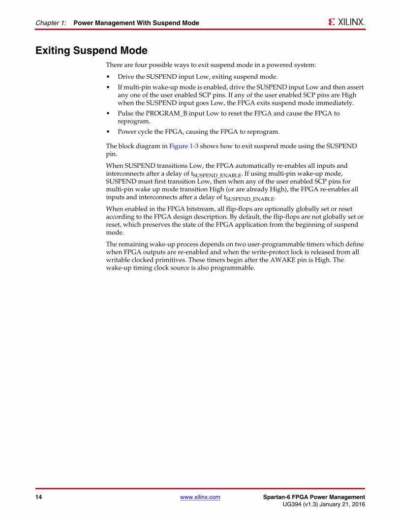
Exiting Suspend ModeThere are four possible ways to exit suspend mode in a powered system:
• Drive the SUSPEND input Low, exiting suspend mode.
• If multi-pin wake-up mode is enabled, drive the SUSPEND input Low and then assert any one of the user enabled SCP pins. If any of the user enabled SCP pins are High when the SUSPEND input goes Low, the FPGA exits suspend mode immediately.
• Pulse the PROGRAM_B input Low to reset the FPGA and cause the FPGA to reprogram.
• Power cycle the FPGA, causing the FPGA to reprogram.
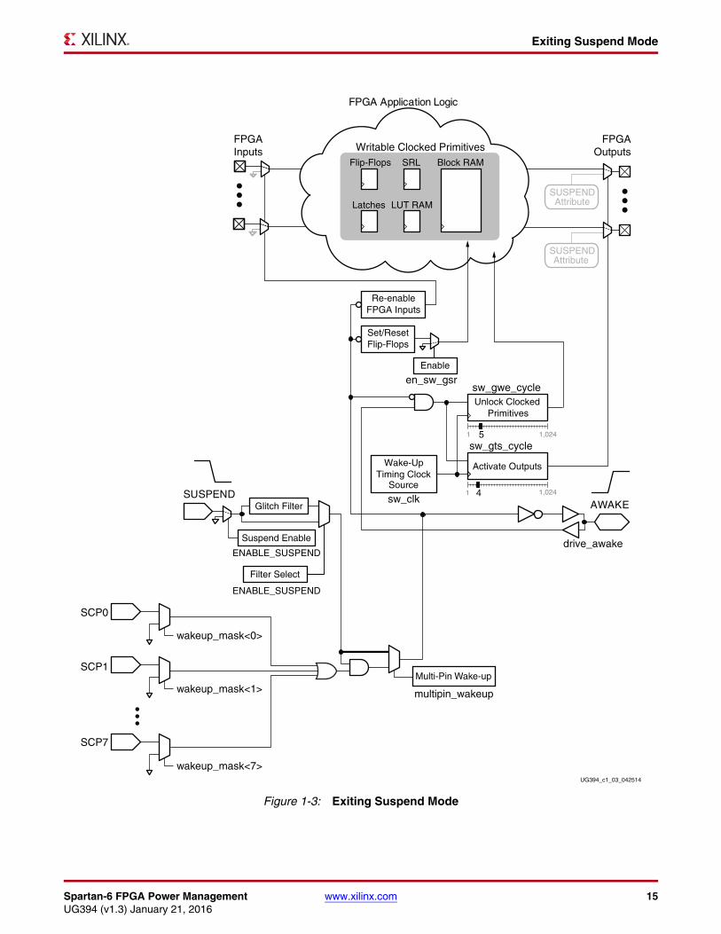
The block diagram in Figure 1-3 shows how to exit suspend mode using the SUSPEND pin.
When SUSPEND transitions Low, the FPGA automatically re-enables all inputs and interconnects after a delay of tSUSPEND_ENABLE. If using multi-pin wake-up mode, SUSPEND must first transition Low, then when any of the user enabled SCP pins for multi-pin wake up mode transition High (or are already High), the FPGA re-enables all inputs and interconnects after a delay of tSUSPEND_ENABLE.
When enabled in the FPGA bitstream, all flip-flops are optionally globally set or reset according to the FPGA design description. By default, the flip-flops are not globally set or reset, which preserves the state of the FPGA application from the beginning of suspend mode.
The remaining wake-up process depends on two user-programmable timers which define when FPGA outputs are re-enabled and when the write-protect lock is released from all writable clocked primitives. These timers begin after the AWAKE pin is High. The wake-up timing clock source is also programmable.
Spartan-6 FPGA Power Management www.xilinx.com 15UG394 (v1.3) January 21, 2016
Exiting Suspend Mode
X-Ref Target - Figure 1-3
Figure 1-3: Exiting Suspend Mode
SUSPENDAttribute
SUSPENDAttribute
Wake-UpTiming Clock
Source
Glitch Filter
Suspend Enable
SRL
LUT RAM
Flip-Flops
Latches
Block RAM
Writable Clocked Primitives
FPGA Application Logic
FPGAInputs
FPGAOutputs
Re-enableFPGA Inputs
Set/ResetFlip-Flops
SUSPENDAWAKE
Enable
Unlock Clocked Primitives
Activate Outputs
sw_clk
en_sw_gsr
ENABLE_SUSPEND
ENABLE_SUSPEND
sw_gts_cycle
sw_gwe_cycle
Filter Select
1 4
1 1,024
1,024
5
UG394_c1_03_042514
drive_awake
multipin_wakeup
wakeup_mask<0>
wakeup_mask<1>
wakeup_mask<7>
SCP0
SCP1
SCP7
Multi-Pin Wake-up
16 www.xilinx.com Spartan-6 FPGA Power ManagementUG394 (v1.3) January 21, 2016
Chapter 1: Power Management With Suspend Mode
PROGRAM_B Programming Pin Always Overrides Suspend ModePulsing the PROGRAM_B programming pin Low always overrides suspend mode and forces the FPGA to restart configuration. Power-cycling the FPGA also restarts configuration. The SUSPEND pin should be Low during power up and configuration.
Enable the Suspend Feature and Glitch FilteringBefore it can be used, the suspend power-saving feature must first be enabled in the FPGA bitstream. By default, the suspend feature is disabled and driving the SUSPEND pin has no effect. The suspend feature is enabled using the user constraints file (UCF), or through a bitstream generator (BitGen) option.
User Constraints File EnableSuspend mode is enabled and the SUSPEND input glitch filter option is defined using a CONFIG statement in a UCF. Table 1-1 shows the available options. This is the recommended method for enabling suspend mode as this attribute also automatically reserves the AWAKE pin.
Config ENABLE_SUSPEND = "FILTERED" ;
Bitstream GeneratorSetting the en_suspend bitstream option is an alternate way to enable the suspend mode. However, this method is not recommended because it does not automatically reserve the AWAKE pin in the application.
bitgen -g en_suspend:Yes
The following option enables the glitch filter on the SUSPEND pin.
bitgen -g suspend_filter:Yes
Table 1-1: Available Options for the ENABLE_SUSPEND Attribute
Option Suspend Mode SUSPEND Pin Filter AWAKE Pin
NO Suspend mode is disabled Not applicable. Connect SUSPEND pin to GND.
Available as a user I/O pin in the FPGA application.
FILTERED Suspend mode is enabled Glitch filter is enabled. AWAKE status indicator.
UNFILTERED Glitch filter is bypassed.
Spartan-6 FPGA Power Management www.xilinx.com 17UG394 (v1.3) January 21, 2016
Enable the Suspend Feature and Glitch Filtering
Define the Multi-Pin Wake-Up Feature and PinsThe multi-pin wake-up feature is not required to use the suspend mode feature. If multi-pin wake-up is not enabled, suspend mode is enabled and disabled using just the SUSPEND pin. Multi-pin wake-up is enabled using a BitGen option.
bitgen -g multipin_wakeup:Yes
If multi-pin wake-up is enabled, select which pins are monitored for a High or a rising edge to bring the FPGA out of suspend mode. Eight SCP pins are used for the multi-pin wake-up feature. Select from one to eight of these pins to monitor. The SCP pins are dual-purpose user I/O pins and can be used as general-purpose I/O independent of the suspend options. Any pins that are not used can be masked out as inputs to the multi-pin wake-up. The option accepts two hex values for the mask. A value of FF enables all SCP pins, 0F enables SCP<3..0>.
bitgen -g wakeup_mask:FF
Define the I/O Behavior During Suspend ModeUse a SUSPEND attribute to define the behavior of each I/O and output pin during suspend mode.
Single-Ended I/O Standards
Each output, open-drain output, or bidirectional I/O pin in the FPGA application that uses a single-ended I/O standard can be individually programmed for one of the suspend mode behaviors shown in Table 1-2. The default behavior is for a high impedance pin during suspend mode although other options are available.
Differential I/O Standards
The output drivers for the LVDS, RSDS, mini-LVDS, PPDS, and TMDS differential I/O standards are high impedance, using any of the 3STATE attributes described in Table 1-2. The DRIVE_LAST_VALUE attribute is not supported for differential output drivers.
Treat the pseudo-differential I/O standards, such as BLVDS, DIFF_HSTL, and DIFF_SSTL, as two single-ended I/O pins. All the attributes apply as for Single-Ended I/O Standards
Table 1-2: Output Behavior Options during Suspend Mode
SUSPEND Attribute Function
DRIVE_LAST_VALUEThe output continues to drive the level that was last stored in the output latch, according to the chosen standard. Requires VCCO to remain at the recommended operating conditions for the bank.
3STATE
(default)
The output is in the high-impedance state with no active internal pull-up or pull-down resistor. Results in the lowest possible I/O current draw.
3STATE_PULLUPThe output is in the high-impedance state with an internal pull-up resistor to the associated VCCO supply. Requires VCCO to remain at the recommended operating conditions for the bank.
3STATE_PULLDOWN The output is in the high-impedance state with an internal pull-down resistor to GND.
3STATE_KEEPERThe output is high impedance. The internal bus keeper circuit is active. Requires VCCO to remain at the recommended operating conditions for the bank.
18 www.xilinx.com Spartan-6 FPGA Power ManagementUG394 (v1.3) January 21, 2016
Chapter 1: Power Management With Suspend Mode
although for any differential standard the settings must be set appropriately for both pins of the complementary pair.
When in the high-impedance state, the differential driver pair does not conduct current to the power or ground rails, or between adjacent pins.
SUSPEND AttributeThe SUSPEND attribute allows each pin to have an individually defined behavior during suspend mode. The available options are listed in Table 1-2.
UCF Example
This UCF constraint example defines the suspend mode behavior for a specific pin. The SUSPEND attribute can be included on the same UCF line as other constraints for a pin.
Net "<net_name>" SUSPEND = "io_type" ;
UCF entries for a single-ended pin and a differential pair are shown in the following example:
NET "TX<0>" IOSTANDARD = LVCMOS_33 | SUSPEND = "DRIVE_LAST_VALUE" ;NET "TX_P<0>" IOSTANDARD = LVDS_33 | SUSPEND = "3STATE_PULLUP" ;NET "TX_N<0>" IOSTANDARD = LVDS_33 | SUSPEND = "3STATE_PULLDOWN" ;
Design Maintained during Suspend ModeAfter entering suspend mode, all writable clocked primitives are write-protected after a delay of tSUSPEND_GWE. The state of all clocked memory primitives is maintained during suspend mode.
• Logic block flip-flops
• I/O block latches and flip-flops
• Logic block distributed RAM (LUT RAM)
• Logic block shift registers (SRL)
• Block RAM and registers
When exiting suspend mode, all writable clocked primitives are re-enabled, controlled by the sw_gwe_cycle setting.
An additional bitstream option, en_sw_gsr, controls whether all clocked primitives are globally set or reset when the FPGA awakens from suspend mode. By default, en_sw_gsr:No signifies that clocked primitives are not set or reset when the FPGA awakens and all states are preserved.
Spartan-6 FPGA Power Management www.xilinx.com 19UG394 (v1.3) January 21, 2016
Suspend Mode Wake-Up Timing Controls
Design Requirements to Maintain Application DataWhen a design requires that application data be preserved when entering suspend mode, the SUSPEND_SYNC primitive should be used. When the FPGA enters suspend mode, the global write enable (GWE) is removed, maintaining the state of all flip-flops and user RAM. The FPGA requires a delay of tSUSPEND_GWE between recognizing a High on the SUSPEND pin and disabling GWE internally. This is the first event after SUSPEND transitions High, before AWAKE toggles, and before the inputs are disabled if SUSPEND_SYNC is not used. During this delay, additional user clocks to flip-flops or RAM can continue to update their contents. Since the GWE signal can have some skew between locations on the device, some locations can be disabled while others remain enabled on the last clock edge before GWE takes full effect. This situation can be avoided when using the SUSPEND_SYNC feature. After the suspend request is driven out of the SUSPEND_SYNC primitive, disable the clocks and/or clock enables on the logic that must retain its current state. After the disable is complete, drive the SACK port of the SUSPEND_SYNC primitive and the FPGA begins the process to enter suspend mode.
To avoid initializing the flip-flops when exiting suspend mode, choose en_sw_gsr:No. Exiting suspend mode should be synchronized to a user clock to avoid race conditions corrupting the application data. Inputs are enabled first, allowing control signals to continue to hold off the toggling of storage primitives. The assertion of GWE can be synchronized to a user clock to align it with a system clock edge.
Suspend Mode Wake-Up Timing ControlsWhen exiting suspend mode, the wake-up sequence for the FPGA is programmable and controlled by a single clock.
Wake-Up Timing Clock SourceThe wake-up timing when exiting suspend mode is controlled by a selectable clock source as shown in Figure 1-4 and described in Table 1-3. The clock source is defined by one or two bitstream generator options, sw_clk and sometimes StartupClk.
The internal oscillator is disabled during suspend mode to conserve power.
20 www.xilinx.com Spartan-6 FPGA Power ManagementUG394 (v1.3) January 21, 2016
Chapter 1: Power Management With Suspend Mode
• The sw_clk option is specific to the suspend feature. By default, sw_clk:InternalClk.
• The StartupClk option is available on every application. The same option used to clock the start-up process at the end of configuration can be used to clock the wake-up process at the end of suspend. StartupClk:Cclk is the default; however, using this for suspend wake-up requires a persisted slave configuration mode. When using sw_clk:StartupClk and StartupClk:Cclk, and exiting suspend mode, the CCLK pin becomes the clock source. The Persist option also retains the dual-purpose configuration pins associated with the configuration logic.
X-Ref Target - Figure 1-4
Figure 1-4: Suspend Mode Wake-Up Timing Control Clock Selection
StartupClk
InternalClk
sw_clk
~50 MHzInternal
Oscillator
Cclk
Jtag
UserClk
CCLK
TCK
STARTUP_SPARTAN6
StartupClk
CLK
CCLK input only available forapplications that configure in Slavemode. Persist = Yes required.
User Clock from FPGA Interconnect
SuspendWake-Up
TimingControl
UG394_c1_04_121009
Table 1-3: Clock Sources to Wake-Up from Suspend Mode
sw_clkSetting
StartupClkSetting
Clock Source Restriction
InternalClk NA Internal OscillatorThe oscillator has an imprecise frequency of about 50 MHz.
StartupClk
Cclk CCLK pin on FPGA
This option is only available for FPGAs using Slave configuration mode. The bitstream option Persist:Yes must be set. This option is not available for FPGAs using the master configuration mode; use InternalClk instead.
JtagClk TCK pin on FPGAThe JTAG interface must be active to exit suspend mode.
UserClkCLK input on the STARTUP_SPARTAN6design primitive
The clock input to the STARTUP design primitive can originate from any non-clocked signal in the FPGA. It cannot originate from a flip-flop source because all clocked primitives are write-protected while in suspend mode.
Spartan-6 FPGA Power Management www.xilinx.com 21UG394 (v1.3) January 21, 2016
Dedicated Configuration Pins Unaffected During Suspend Mode
Switch Outputs from Suspend to Normal BehaviorThe suspend/wake sw_gts_cycle bitstream option controls when I/O pins are released from their SUSPEND attribute settings and returned to normal operation. The timing is controlled by the Wake-Up Timing Clock Source, page 19. The default sw_gts_cycle setting is four cycles, but this control can be set for any value between one and 1,024 clock cycles.
The suspend/wake control becomes active after the AWAKE pin transitions High. After the specified number of clock cycles, all output, open-drain output, and bidirectional I/O pins transition from their suspend behavior, either the default 3STATE or individually specified using the SUSPEND attribute, back to the normal behavior specified in the original FPGA application.
The outputs should be released before releasing the write-protect lock on all clocked primitives.
Release Write Protect on Clocked PrimitivesThe suspend/wake sw_gwe_cycle bitstream option controls when the write-protect lock is released on all clocked primitives.
The timing is controlled by sw_clk the Wake-Up Timing Clock Source, page 19. The default sw_gwe_cycle setting is five cycles, but the suspend/wake control can be set for any value between one and 1,024 clock cycles.
This suspend/wake control becomes active after the AWAKE pin transitions High. After the specified number of clock cycles, the write-protect lock is released from all writable, clocked primitives such as flip-flops, block RAM, etc.
When the en_sw_gsr:yes option is set, the clocked primitives are already globally set or reset to the value specified in the original FPGA design before the write-protect lock is released. The option en_sw_gsr:no signifies that the state of the FPGA after entering suspend mode is preserved.
The outputs should be released before releasing the write-protect lock on all clocked primitives.
Dedicated Configuration Pins Unaffected During Suspend ModeThe following dedicated configuration pins are unaffected when the FPGA is in suspend mode:
• JTAG pins: TDI, TMS, TCK, and TDO
• DONE pin
• PROGRAM_B pin
JTAG Operations Allowed During Suspend ModeTable 1-4 shows the JTAG operations permitted when the FPGA is in suspend mode. Executing these JTAG operations increases the FPGA's power consumption while in suspend mode.
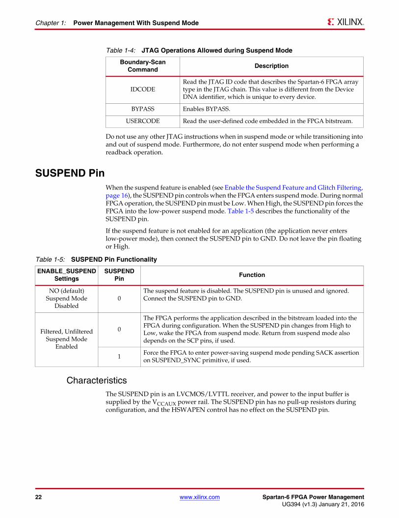
22 www.xilinx.com Spartan-6 FPGA Power ManagementUG394 (v1.3) January 21, 2016
Chapter 1: Power Management With Suspend Mode
Do not use any other JTAG instructions when in suspend mode or while transitioning into and out of suspend mode. Furthermore, do not enter suspend mode when performing a readback operation.
SUSPEND PinWhen the suspend feature is enabled (see Enable the Suspend Feature and Glitch Filtering, page 16), the SUSPEND pin controls when the FPGA enters suspend mode. During normal FPGA operation, the SUSPEND pin must be Low. When High, the SUSPEND pin forces the FPGA into the low-power suspend mode. Table 1-5 describes the functionality of the SUSPEND pin.
If the suspend feature is not enabled for an application (the application never enters low-power mode), then connect the SUSPEND pin to GND. Do not leave the pin floating or High.
CharacteristicsThe SUSPEND pin is an LVCMOS/LVTTL receiver, and power to the input buffer is supplied by the VCCAUX power rail. The SUSPEND pin has no pull-up resistors during configuration, and the HSWAPEN control has no effect on the SUSPEND pin.
Table 1-4: JTAG Operations Allowed during Suspend Mode
Boundary-ScanCommand
Description
IDCODERead the JTAG ID code that describes the Spartan-6 FPGA array type in the JTAG chain. This value is different from the Device DNA identifier, which is unique to every device.
BYPASS Enables BYPASS.
USERCODE Read the user-defined code embedded in the FPGA bitstream.
Table 1-5: SUSPEND Pin Functionality
ENABLE_SUSPENDSettings
SUSPENDPin
Function
NO (default)Suspend Mode
Disabled0
The suspend feature is disabled. The SUSPEND pin is unused and ignored. Connect the SUSPEND pin to GND.
Filtered, Unfiltered Suspend Mode
Enabled
0
The FPGA performs the application described in the bitstream loaded into the FPGA during configuration. When the SUSPEND pin changes from High to Low, wake the FPGA from suspend mode. Return from suspend mode also depends on the SCP pins, if used.
1Force the FPGA to enter power-saving suspend mode pending SACK assertion on SUSPEND_SYNC primitive, if used.
Spartan-6 FPGA Power Management www.xilinx.com 23UG394 (v1.3) January 21, 2016
SUSPEND Input Glitch Filter
SUSPEND Input Glitch FilterThe SUSPEND pin has a programmable glitch filter to guard against short pulses, which could cause the FPGA to spuriously enter suspend mode. Turning off the filter allows the FPGA to enter or exit suspend mode more quickly, but the application must guard against spurious pulses. The difference in delay is the tSUSPENDFILTER value in DS162, Spartan-6 FPGA Data Sheet: DC and Switching Characteristics. See Enable the Suspend Feature and Glitch Filtering, page 16.
SUSPEND_SYNC PrimitiveThe SUSPEND_SYNC primitive is the application interface to a suspend request. If this primitive is not present in the design, the FPGA begins the suspend sequence solely on the state of the SUSPEND pin.
When the SUSPEND_SYNC primitive is in the design, after the SUSPEND pin is asserted High and the filter delay (when the glitch filter is enabled), the SUSPEND_SYNC primitive drives the SREQ port High on the next rising clock edge on the CLK port. This indicates that a request has been received to enter suspend mode. The FPGA does not enter suspend mode until the SACK port is driven High on a rising edge of CLK.
This primitive provides an ideal interface for the application to complete any functions prior to entering suspend mode. Any I/O interface ports can be closed, buffers flushed, and clocks disabled to ensure the application is in a ready state prior to being suspended. For more details, see Design Maintained during Suspend Mode, page 18.
AWAKE PinThe AWAKE pin (optionally) provides status on the suspend power-savings mode.
General Behavior (Suspend Feature Disabled)Unless the suspend feature is enabled, the AWAKE pin is a general-purpose user-I/O pin.
AWAKE Pin Behavior when Suspend Feature is EnabledIf the suspend feature is enabled, then the AWAKE pin indicates the present state of the FPGA, as summarized in Table 1-6. The AWAKE pin cannot be used by the FPGA application as a general-purpose I/O pin.
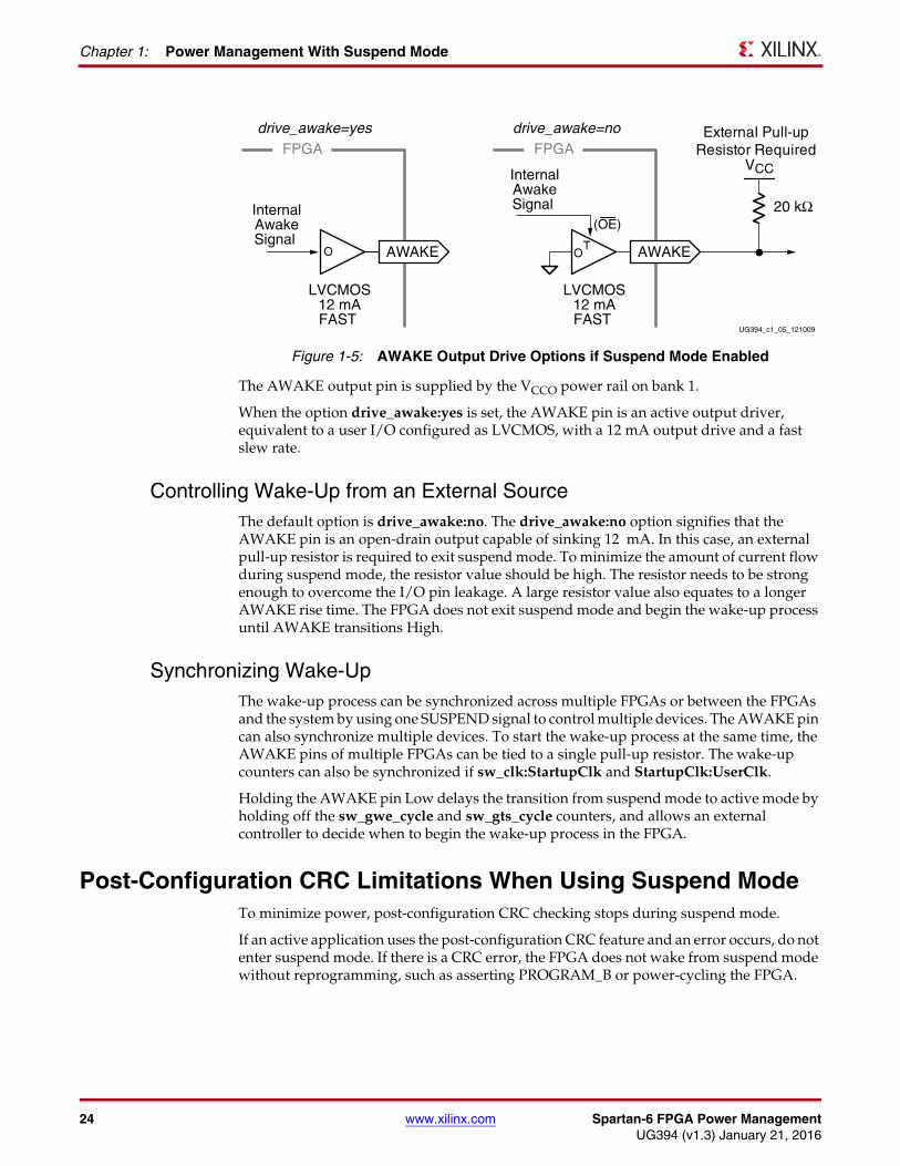
The AWAKE pin can further be configured as an open-drain output (the default) or a full-swing output driver, as shown in Figure 1-5. This behavior is controlled by a bitstream generator (BitGen) option:
bitgen -g drive_awake:no
Table 1-6: AWAKE Pin Status
AWAKE Pin Indication
0 The FPGA is presently in the low-power suspend mode.
1 The FPGA is active.
24 www.xilinx.com Spartan-6 FPGA Power ManagementUG394 (v1.3) January 21, 2016
Chapter 1: Power Management With Suspend Mode
The AWAKE output pin is supplied by the VCCO power rail on bank 1.
When the option drive_awake:yes is set, the AWAKE pin is an active output driver, equivalent to a user I/O configured as LVCMOS, with a 12 mA output drive and a fast slew rate.
Controlling Wake-Up from an External SourceThe default option is drive_awake:no. The drive_awake:no option signifies that the AWAKE pin is an open-drain output capable of sinking 12 mA. In this case, an external pull-up resistor is required to exit suspend mode. To minimize the amount of current flow during suspend mode, the resistor value should be high. The resistor needs to be strong enough to overcome the I/O pin leakage. A large resistor value also equates to a longer AWAKE rise time. The FPGA does not exit suspend mode and begin the wake-up process until AWAKE transitions High.
Synchronizing Wake-UpThe wake-up process can be synchronized across multiple FPGAs or between the FPGAs and the system by using one SUSPEND signal to control multiple devices. The AWAKE pin can also synchronize multiple devices. To start the wake-up process at the same time, the AWAKE pins of multiple FPGAs can be tied to a single pull-up resistor. The wake-up counters can also be synchronized if sw_clk:StartupClk and StartupClk:UserClk.
Holding the AWAKE pin Low delays the transition from suspend mode to active mode by holding off the sw_gwe_cycle and sw_gts_cycle counters, and allows an external controller to decide when to begin the wake-up process in the FPGA.
Post-Configuration CRC Limitations When Using Suspend ModeTo minimize power, post-configuration CRC checking stops during suspend mode.
If an active application uses the post-configuration CRC feature and an error occurs, do not enter suspend mode. If there is a CRC error, the FPGA does not wake from suspend mode without reprogramming, such as asserting PROGRAM_B or power-cycling the FPGA.
X-Ref Target - Figure 1-5
Figure 1-5: AWAKE Output Drive Options if Suspend Mode Enabled
AWAKE AWAKE
InternalAwakeSignal Internal
AwakeSignal
LVCMOS12 mAFAST
LVCMOS12 mAFAST
O OT
(OE)
FPGA FPGAVCC
20 kΩ
drive_awake=yes drive_awake=no External Pull-upResistor Required
UG394_c1_05_121009
Spartan-6 FPGA Power Management www.xilinx.com 25UG394 (v1.3) January 21, 2016
Post-Configuration CRC Limitations When Using Suspend Mode
Several design options are possible:
1. Do not use the post-configuration CRC feature when the suspend mode feature is enabled and vice versa.
2. Always reprogram the device when a CRC error occurs.
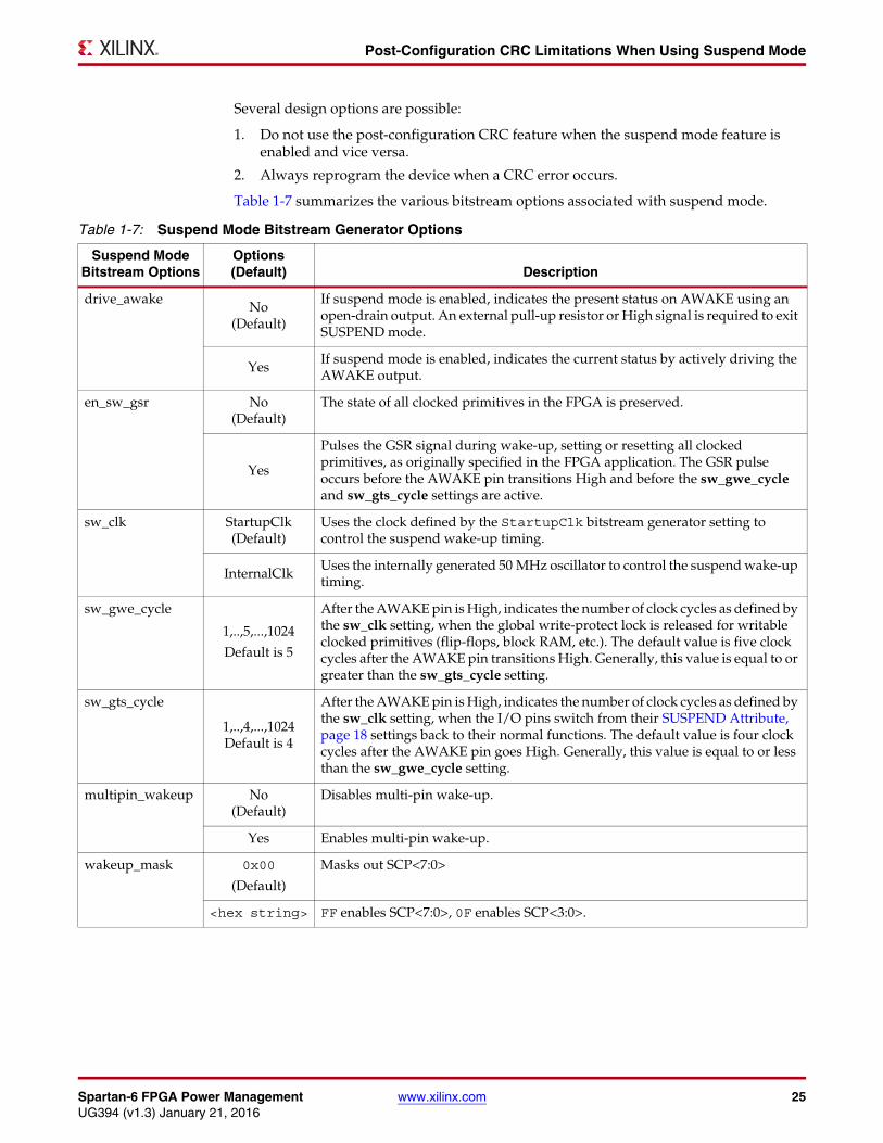
Table 1-7 summarizes the various bitstream options associated with suspend mode.
Table 1-7: Suspend Mode Bitstream Generator Options
Suspend Mode Bitstream Options
Options(Default) Description
drive_awakeNo
(Default)
If suspend mode is enabled, indicates the present status on AWAKE using an open-drain output. An external pull-up resistor or High signal is required to exit SUSPEND mode.
YesIf suspend mode is enabled, indicates the current status by actively driving the AWAKE output.
en_sw_gsr No(Default)
The state of all clocked primitives in the FPGA is preserved.
Yes
Pulses the GSR signal during wake-up, setting or resetting all clocked primitives, as originally specified in the FPGA application. The GSR pulse occurs before the AWAKE pin transitions High and before the sw_gwe_cycle and sw_gts_cycle settings are active.
sw_clk StartupClk(Default)
Uses the clock defined by the StartupClk bitstream generator setting to control the suspend wake-up timing.
InternalClk Uses the internally generated 50 MHz oscillator to control the suspend wake-up timing.
sw_gwe_cycle
1,..,5,...,1024
Default is 5
After the AWAKE pin is High, indicates the number of clock cycles as defined by the sw_clk setting, when the global write-protect lock is released for writable clocked primitives (flip-flops, block RAM, etc.). The default value is five clock cycles after the AWAKE pin transitions High. Generally, this value is equal to or greater than the sw_gts_cycle setting.
sw_gts_cycle
1,..,4,...,1024Default is 4
After the AWAKE pin is High, indicates the number of clock cycles as defined by the sw_clk setting, when the I/O pins switch from their SUSPEND Attribute, page 18 settings back to their normal functions. The default value is four clock cycles after the AWAKE pin goes High. Generally, this value is equal to or less than the sw_gwe_cycle setting.
multipin_wakeup No(Default)
Disables multi-pin wake-up.
Yes Enables multi-pin wake-up.
wakeup_mask 0x00
(Default)
Masks out SCP<7:0>
<hex string> FF enables SCP<7:0>, 0F enables SCP<3:0>.
26 www.xilinx.com Spartan-6 FPGA Power ManagementUG394 (v1.3) January 21, 2016
Chapter 1: Power Management With Suspend Mode
FPGA Voltage Requirements During Suspend ModeDuring suspend mode, the VCCINT and VCCAUX rails must remain powered at the data sheet levels for Recommended Operating Conditions. However, the VCCO supply to each of the I/O banks can be (potentially) turned off to conserve additional power, depending on system requirements. Optionally, VCCO can be reduced during suspend mode, but this also affects the voltage levels for any output pin with a SUSPEND attribute set to DRIVE_LAST_VALUE.
The FPGA's power-on reset (POR) circuit continues to monitor the VCCINT and VCCAUX supplies. Although VCCO2 is an input to the POR circuit at initial power-on, the POR circuit does not monitor the VCCO supplies after configuration. By default, if the VCCINT or VCCAUX supply dips below the minimum specified data sheet voltage limit, then the FPGA restarts configuration.
Memory Controller BlockRecommendations and methods for using the memory controller block interface with the Spartan-6 FPGA suspend mode are found in UG388, Spartan-6 FPGA Memory Controller Block User Guide.
Spartan-6 FPGA Power Management www.xilinx.com 27UG394 (v1.3) January 21, 2016
Chapter 2
Voltage Supplies
IntroductionSpartan-6 FPGAs have multiple voltage supply inputs, as shown in Table 2-1. There are two supply inputs for internal logic functions, VCCINT and VCCAUX. Each of the I/O banks has a separate VCCO supply input that powers the output buffers within the associatedI/O bank. VCCO is also used for input buffers for some I/O standards. A VREF reference voltage is needed for HSTL/SSTL standards. The GTP transceivers have dedicated analog power rails (see UG386, Spartan-6 FPGA GTP Transceivers User Guide for more details). The AES circuitry has its own power supplies for the encryption key, depending on how it is stored (see UG380, Spartan-6 FPGA Configuration User Guide for more details).
Table 2-1: Spartan-6 FPGA Voltage Supplies
Supply Input Description DevicesNominal Supply
Voltage
VCCINT
Internal core supply voltage. Supplies all internal logic functions, such as CLBs, block RAM, and DSP blocks. Input to the power-on reset (POR) circuit. Powers input signals for most standards at 1.2V, 1.5V, and 1.8V.
All 1.2V; 1.0V (-1L) in lower-power
Spartan-6 LX devices
VCCAUX
Auxiliary supply voltage. Supplies clock management tiles (CMTs), some I/O resources, some dedicated configuration pins, and JTAG interface. Powers input signals for most standards at 2.5V and 3.3V. Input to the POR circuit.
All 2.5V;
3.3V optional
VCCO_0
Supplies the output buffers in I/O bank 0, the bank along the top edge of the FPGA.
All Selectable: 3.3V, 2.5V, 1.8V, 1.5V,
or 1.2V
VCCO_1
Supplies the output buffers in I/O bank 1, the bank along the right edge of the FPGA. During configuration in byte-wide peripheral interface (BPI) Parallel Flash Mode, connects to the same voltage as the Flash PROM.
All Selectable: 3.3V, 2.5V, 1.8V, 1.5V,
or 1.2V
VCCO_2
Supplies the output buffers in I/O bank 2, the bank along the bottom edge of the FPGA. Connects to the same voltage as the FPGA configuration source. Input to the POR circuit.
All Selectable: 3.3V, 2.5V, 1.8V, 1.5V,
or 1.2V
VCCO_3
Supplies the output buffers in I/O bank 3, the bank along the left edge of the FPGA.
All Selectable: 3.3V, 2.5V, 1.8V, 1.5V,
or 1.2V
28 www.xilinx.com Spartan-6 FPGA Power ManagementUG394 (v1.3) January 21, 2016
Chapter 2: Voltage Supplies
VCCINTVCCINT is the primary power supply for the FPGA. In the Spartan-6 LXT family and the standard devices in the Spartan-6 LX family (-2 and -3 speed grades), VCCINT has a nominal value of 1.2V. The lower-power Spartan-6 LX devices (-1L speed grade) uses a nominal VCCINT of 1.0V. See Chapter 3, Lower-Power Spartan-6 LX Devices.
VCCAUXVCCAUX powers the auxiliary logic, including configuration logic and some internal and I/O resources. The Spartan-6 FPGA’s VCCAUX is either 2.5V or 3.3V. These two voltages provide greater flexibility and allow VCCAUX to be set to the same level as an existing VCCO rail, to minimize the number of power rails. Reducing VCCAUX to 2.5V can reduce the power consumption on the VCCAUX rail by 40%.
During configuration, if VCCO_2 is 1.8V, VCCAUX must be 2.5V. If VCCO_2 is 2.5V or 3.3V, VCCAUX can be either 2.5V or 3.3V. See UG380, Spartan-6 FPGA Configuration User Guide.
The -1L speed grade devices require VCCAUX = 2.5V when using the LVDS_25, LVDS_33, BLVDS_25, LVPECL_25, RSDS_25, RSDS_33, PPDS_25, and PPDS_33 I/O standards on inputs. See DS162, Spartan-6 FPGA Data Sheet: DC and Switching Characteristics.
VCCO_4
Supplies the output buffers in I/O bank 4, the bank along the top of the left edge of the FPGA in 6-bank devices.
LX75/T, LX100/T, and the LX150/T in FG(G)676 and
FG(G)900
Selectable: 3.3V, 2.5V, 1.8V, 1.5V,
or 1.2V
VCCO_5
Supplies the output buffers in I/O bank 5, the bank along the top of the right edge of the FPGA in 6-bank devices.
LX75/T, LX100/T, and the LX150/T in FG(G)676 and
FG(G)900
Selectable: 3.3V, 2.5V, 1.8V, 1.5V,
or 1.2V
VREF
Input threshold voltage pins when HSTL/SSTL standards are used in the bank, otherwise user I/Os. When used as a reference voltage within a bank, all VREF pins within that bank must be connected.
All Varies
MGTAVCCPower-supply pin for the transceiver mixed-signal circuitry.
LXT 1.2V
MGTAVCCPLL0/1 Power-supply pin for the transceiver PLL LXT 1.2V
MGTAVTTTX/RXPower-supply pin for the transceiver TX and RX circuitry.
LXT 1.2V
MGTAVTTRCALPower-supply pin for the transceiver resistor calibration circuit.
LXT 1.2V
VBATTDecryptor key memory backup supply. When key is not used, tie this pin to VCC or GND, or it can be left floating.
LX75/T, LX100/T, LX150/T
3.3V
VFS
Decryptor key EFUSE power supply pin for programming. When key is not being programmed, tie this pin to VCC or GND, or it can be left floating.
LX75/T, LX100/T, LX150/T
3.3V
Table 2-1: Spartan-6 FPGA Voltage Supplies (Cont’d)
Supply Input Description DevicesNominal Supply
Voltage
Spartan-6 FPGA Power Management www.xilinx.com 29UG394 (v1.3) January 21, 2016
VCCO
Setting the VCCAUX LevelThe user must set the CONFIG VCCAUX attribute according to the voltage being provided to the VCCAUX rails. The valid values for this attribute are 2.5 (default) or 3.3. This attribute affects the banking rules for I/O placement within the automated placer, as well as in the pin assignments tool. It also affects the end-generated bitstream for the device. The VCCAUX attribute is a global attribute for the Spartan-6 device and is not attached to any particular primitive.
CONFIG VCCAUX=3.3;
VCCAUX SpecificationsBoth the 2.5V and 3.3V settings for VCCAUX allow a variation (2.375V to 2.625V, or 3.15V to 3.45V). The data retention voltage is the same for both at 2.0V, so more care must be taken with a 2.5V rail to not let it drop more than 0.5V. See DS162, Spartan-6 FPGA Data Sheet: DC and Switching Characteristics for complete specifications.
The CONFIG VCCAUX attribute is used by the ISE® Design Suite software to determine if LVCMOS25 inputs can be powered by VCCAUX. If CONFIG VCCAUX = 2.5, VCCAUX is used to power LVCMOS25 inputs. If CONFIG VCCAUX = 3.3, VCCO must be 2.5V for any banks with LVCMOS25 inputs. Setting VCCAUX to match whichever is more common between LVCMOS25 and LVCMOS33 can help optimize placement.
There are some slight changes to resistor values depending on whether VCCAUX is set to 2.5V or 3.3V. The I/O pull-down resistor values are lower for a VCCAUX of 3.3V. The differential termination resistor (DIFF_TERM) can be more tightly controlled around 100Ω when VCCAUX is 3.3V. See DS162, Spartan-6 FPGA Data Sheet: DC and Switching Characteristics and the Spartan-6 FPGA IBIS models at:
http://www.xilinx.com/support/download/index.htm
VCCOVCCO powers the I/O resources, and has separate rails for each bank of I/O for maximum flexibility. All of the VCCO connections to a specific I/O bank must be connected to the same voltage. The VCCO voltage can be 1.2V to 3.3V, depending on the output standard specified for a given bank. Most devices have four I/O banks, while the XC6SLX75/T and larger in the FG(G)676 and FG(G)900 packages offer six I/O banks. The VCCO pins for a bank should all be tied to a supply rail, even if the bank is completely unused.
In a 3.3V-only application, all VCCO supplies and VCCAUX connect to 3.3V. Spartan-6 FPGAs allow bridging between different I/O voltages and standards by applying different voltages to the VCCO inputs of different banks. Refer to the I/O banking rules section in UG381, Spartan-6 FPGA SelectIO Resources User Guide for the I/O standards that can be mixed within a single I/O bank.
The Spartan-6 FPGA VCCO ranges support variation around the nominal supply voltage. Refer to DS162, Spartan-6 FPGA Data Sheet: DC and Switching Characteristics for specific voltage levels.
30 www.xilinx.com Spartan-6 FPGA Power ManagementUG394 (v1.3) January 21, 2016
Chapter 2: Voltage Supplies
VREFEach I/O bank also has a separate, optional input voltage reference supply, called VREF. If the I/O bank includes an I/O standard that requires a voltage reference such as HSTL or SSTL, then all VREF pins within the I/O bank must be connected to the same voltage. The VREF pins are available as I/O pins if no standards within a bank require them.
Xilinx recommends always separating VREF from VTT as the VTT supply can be very noisy. A stable VREF using a small LDO is the desirable implementation. A voltage divider implementation is also possible. Knowledge of the PCB environment, such as frequency of coupled noise, is required to correctly calculate the resistance and capacitance values of the divider circuit. As a result, an isolated reference supply is usually a more robust and simpler approach. Refer to UG381, Spartan-6 FPGA SelectIO Resources User Guide for more details on VREF.
Board Design and Signal IntegrityBuilding a working system today requires knowledge of the many options available. The advantages of feature size reduction and reduced power consumption have reduced core voltages down to the 1.0V range. This change in voltage and signal frequency content requires the use of advanced design practices to manage electrical effects. The documents and links on the Xilinx Signal Integrity website provides everything needed to achieve reliable PCB designs the first time:
http://www.xilinx.com/products/technology/signal-integrity/index.htm
Simultaneously Switching OutputsGround or power bounce occurs when a large number of outputs simultaneously switch in the same direction. Each FPGA family provides guidelines for the recommended maximum allowable number of simultaneously switching outputs (SSOs). For more information on SSO, see the Simultaneously Switching Outputs section of UG381, Spartan-6 FPGA SelectIO Resources User Guide and DS162, Spartan-6 FPGA Data Sheet: DC and Switching Characteristics.
Power Distribution System Design and Decoupling/Bypass CapacitorsGood power distribution system (PDS) design is important for all FPGA designs, especially for high-performance applications greater than 100 MHz. Proper design results in better overall performance, lower clock jitter, and a generally more robust system. Before designing the printed circuit board (PCB) for the FPGA design, review UG393, Spartan-6 FPGA PCB Design Guide.
Spartan-6 FPGA Power Management www.xilinx.com 31UG394 (v1.3) January 21, 2016
Chapter 3
Lower-Power Spartan-6 LX Devices
IntroductionThe lower-power Spartan-6 LX devices (-1L) meet lower quiescent and dynamic current levels than the standard Spartan-6 LX devices. They also operate at a reduced VCCINT of 1.0V, versus the 1.2V of the standard Spartan-6 family, thus reducing core power. The lower-power Spartan-6 LX devices are supported by the -1L speed grade. Although the -1L devices are slower than the standard Spartan-6 LX family's slowest speed grade (-2), an additional 30–40% power savings is attained.
Use L1 as the speed grade when ordering the lower-power Spartan-6 LX devices, which is also the way the speed grade is marked on the device. For example, the FPGA ordered as the XC6SLX16-L1CSG324 is marked as either L1C for commercial temperature range or L1I for industrial temperature range.
Designing Using the Lower-Power Spartan-6 LX DevicesTo design for the lower-power Spartan-6 LX devices, select the appropriate device during implementation. A design targeted to the lower-power Spartan-6 LX devices can be defined using all the same methods and options as available to the standard Spartan-6 LX devices. All primitives that support the Spartan-6 LX family also support the lower-power Spartan-6 LX devices. The lower-power Spartan-6 LX devices can be selected using the ISE Design Suite in the Project Navigator. Different from the ordering code or actual device marking, the Xilinx tools display the part number with an appended L (for example, XC6SLX16L). The only speed grade supported for these devices is the -1L. The same speed grade supports both the commercial and industrial temperature ranges.
The resulting bitstream is identical in format between the standard Spartan-6 LX devices and the lower-power Spartan-6 LX devices. The JTAG device IDCODEs are identical and the iMPACT software identifies the device under the same standard Spartan-6 FPGA part number. However, there are small implementation differences between the two families, including a reset circuit used for the DCM CLKFX output (see the RST Input Logic section of UG382, Spartan-6 FPGA Clocking Resources User Guide), and differences in block RAM configuration. Therefore, the designer must target the correct device both to generate the correct timing information, and to account for implementation differences between the two families. The standard and lower-power Spartan-6 LX device bitstreams can not be used in both families. A standard Spartan-6 LX device should not be powered at 1.0V, and a lower-power Spartan-6 LX device should not be powered at 1.2V.
32 www.xilinx.com Spartan-6 FPGA Power ManagementUG394 (v1.3) January 21, 2016
Chapter 3: Lower-Power Spartan-6 LX Devices
Table 3-1 summarizes the designations for a member of the lower-power Spartan-6 LX devices.
Lower-Power Spartan-6 LX Device SpecificationsSeveral specifications are different for the lower-power Spartan-6 LX devices than in the standard Spartan-6 LX family. All of the differences are listed in DS162, Spartan-6 FPGA Data Sheet: DC and Switching Characteristics.
The lower-power Spartan-6 LX devices require a VCCINT of 1.0V ±5%, or 0.95V to 1.05V. It is not tested or guaranteed at 1.2V, and therefore the VCCINT cannot be scaled up and down between 1.2V and 1.0V. In the same way, a standard Spartan-6 LX device cannot be operated at 1.0V.
The lower-power Spartan-6 LX devices have lower-power specifications, as seen in the data sheet for quiescent current, and in the Power Estimators for both quiescent and dynamic current and power. See Chapter 5, Power Estimation.
Because of the reduction in maximum VCCINT, the maximum time for ramping up is shorter. See the VCCINTR ramp time specification in DS162, Spartan-6 FPGA Data Sheet: DC and Switching Characteristics.
Because the I/O thresholds for LVCMOS12, LVCMOS15, and LVCMOS18 are based on the VCCINT level, they are slightly lower for the lower-power Spartan-6 LX devices than the standard Spartan-6 family. See the SelectIO Interface DC Input and Output Levels table in DS162, Spartan-6 FPGA Data Sheet: DC and Switching Characteristics.
The lower-power Spartan-6 LX devices require VCCAUX = 2.5V when using the LVDS_25, LVDS_33, BLVDS_25, LVPECL_25, RSDS_25, RSDS_33, PPDS_25, and PPDS_33I/O standards on inputs. LVPECL_33 is not supported in these devices.
Lower-power Spartan-6 LX devices only support tap 0 of the IODELAY2.
Table 3-1: Lower-Power Spartan-6 LX Device Designation Examples
Designation Example
Ordering Code XC6SLX16-L1CSG324C
Mark
XC6SLX16
CSG324
DxxxxxxxA (lot code)
L1C
Software FamilyIn software choose: Spartan6 Lower Power
Software Device XC6SLX16L-1LCSG324
Speed Specification -1L
Spartan-6 FPGA Power Management www.xilinx.com 33UG394 (v1.3) January 21, 2016
Chapter 4
Power-On and Power-Down Behavior Including Hibernate
IntroductionSpartan-6 FPGAs are designed for maximum system flexibility and reliability when powering up and powering down. During power-on, the device ensures reliable configuration by waiting until a fixed time after the supply rails are valid. During power-down or hibernate, the device disables the outputs and awaits re-application of power to reconfigure. Both power-up and power-down are enhanced by the hot swap compliance of the I/O, allowing the FPGA to be moved in or out of a powered system without damage.
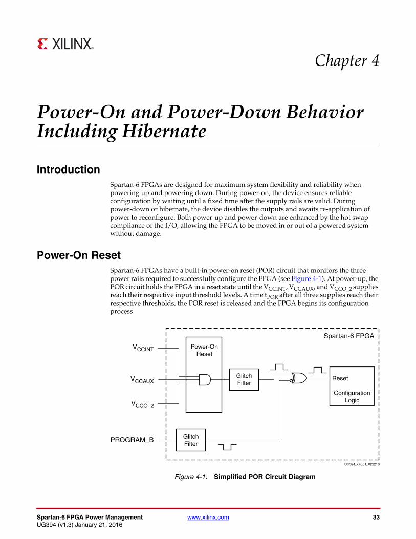
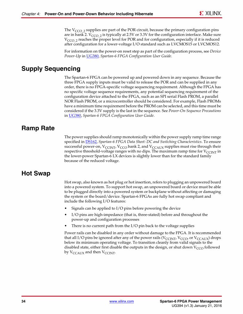
Power-On ResetSpartan-6 FPGAs have a built-in power-on reset (POR) circuit that monitors the three power rails required to successfully configure the FPGA (see Figure 4-1). At power-up, the POR circuit holds the FPGA in a reset state until the VCCINT, VCCAUX, and VCCO_2 supplies reach their respective input threshold levels. A time tPOR after all three supplies reach their respective thresholds, the POR reset is released and the FPGA begins its configuration process.X-Ref Target - Figure 4-1
Figure 4-1: Simplified POR Circuit Diagram
Spartan-6 FPGA
Reset
GlitchFilter
PROGRAM_B
VCCO_2
VCCAUX
VCCINT Power-OnReset
ConfigurationLogic
GlitchFilter
UG394_c4_01_022210
34 www.xilinx.com Spartan-6 FPGA Power ManagementUG394 (v1.3) January 21, 2016
Chapter 4: Power-On and Power-Down Behavior Including Hibernate
The VCCO_2 supplies are part of the POR circuit, because the primary configuration pins are in bank 2. VCCO_2 is typically at 2.5V or 3.3V for the configuration interface. Make sure VCCO_2 reaches the proper level for POR and for configuration, especially if it is reduced after configuration for a lower-voltage I/O standard such as LVCMOS15 or LVCMOS12.
For information on the power-on reset step as part of the configuration process, see Device Power-Up in UG380, Spartan-6 FPGA Configuration User Guide.
Supply SequencingThe Spartan-6 FPGA can be powered up and powered down in any sequence. Because the three FPGA supply inputs must be valid to release the POR and can be supplied in any order, there is no FPGA-specific voltage sequencing requirement. Although the FPGA has no specific voltage sequence requirements, any potential sequencing requirement of the configuration device attached to the FPGA, such as an SPI serial Flash PROM, a parallel NOR Flash PROM, or a microcontroller should be considered. For example, Flash PROMs have a minimum time requirement before the PROM can be selected, and this time must be considered if the 3.3V supply is the last in the sequence. See Power-On Sequence Precautions in UG380, Spartan-6 FPGA Configuration User Guide.
Ramp RateThe power supplies should ramp monotonically within the power supply ramp time range specified in DS162, Spartan-6 FPGA Data Sheet: DC and Switching Characteristics. To ensure successful power-on, VCCINT, VCCO bank 2, and VCCAUX supplies must rise through their respective threshold-voltage ranges with no dips. The maximum ramp time for VCCINT in the lower-power Spartan-6 LX devices is slightly lower than for the standard family because of the reduced voltage.
Hot SwapHot swap, also known as hot plug or hot insertion, refers to plugging an unpowered board into a powered system. To support hot swap, an unpowered board or device must be able to be plugged directly into a powered system or backplane without affecting or damaging the system or the board/device. Spartan-6 FPGAs are fully hot swap compliant and include the following I/O features:
• Signals can be applied to I/O pins before powering the device
• I/O pins are high-impedance (that is, three-stated) before and throughout the power-up and configuration processes
• There is no current path from the I/O pin back to the voltage supplies
Power rails can be disabled in any order without damage to the FPGA. It is recommended that all I/O pins be ignored after any of the power rails (VCCINT, VCCO, or VCCAUX) drops below its minimum operating voltage. To transition cleanly from valid signals to the disabled state, either first disable the outputs in the design, or shut down VCCO followed by VCCAUX and then VCCINT.
Spartan-6 FPGA Power Management www.xilinx.com 35UG394 (v1.3) January 21, 2016
Configuration Data Retention and Brown Out
Configuration Data Retention and Brown OutThe FPGA's configuration data is stored in robust CMOS configuration latches. The data in these latches is retained even when the voltages drop to the minimum levels necessary to preserve RAM contents, as specified in DS162, Spartan-6 FPGA Data Sheet: DC and Switching Characteristics (VDRINT and VDRAUX).
After configuration, if the VCCAUX or VCCINT supply drops below its minimum data retention voltage, the integrity of the CMOS configuration latches is no longer guaranteed, and the current device configuration must be cleared using one of the following methods:
• Force the VCCAUX or VCCINT supply voltage to GND, then raise the voltages back to the recommended operating range (as shown in DS162, Spartan-6 FPGA Data Sheet: DC and Switching Characteristics)
• Assert PROGRAM_B Low, then raise it back High
The POR circuit does not monitor the VCCO_2 supply after configuration. Consequently, dropping the VCCO_2 voltage does not reset the device by triggering a POR event. The PROGRAM_B input bypasses the POR circuit (see Figure 4-1, page 33) and therefore can be used as an independent means to initialize the FPGA.
After the INIT_B signal goes High to indicate successful clearing of the FPGA, reconfigure the FPGA.
GTP Transceiver Power-Up and Power-DownAll GTP_DUAL tiles are reset automatically after configuration. The supplies for the calibration resistor and calibration resistor reference must be powered up before configuration to ensure correct calibration of the termination impedance of all transceivers.
The reference clock and the power to the GTP_DUAL tile must be available before configuring the FPGA. If the reference clock or GTP_DUAL tile is powered up after configuration, apply GTPRESET to allow the PMA PLL to lock.
The GTP transceiver supports a range of power-down modes. These modes support both generic power management capabilities as well as those defined in the PCI Express and SATA standards.
Each channel in each direction can be powered down separately using TXPOWERDOWN and RXPOWERDOWN. Each PLLPOWERDOWN port directly affects the associated PLL that is selected by the PLL_SOURCE attribute.
For more details on the GTP Transceivers, see UG386, Spartan-6 FPGA GTP Transceivers User Guide, Managing Used and Unused GTP Transceivers, Board Design Guidelines.
Hibernate Power DownHibernate is effectively powering down the FPGA (Figure 4-2). Due to the hot swap compliance of the Spartan-6 family, this is allowed even if external devices are still providing active signals to the FPGA. The FPGA loses its configuration data and must be re-programmed after power-on. Hibernate provides the maximum possible power savings for applications that can be turned off for long periods of time and that can afford to lose the present design state.
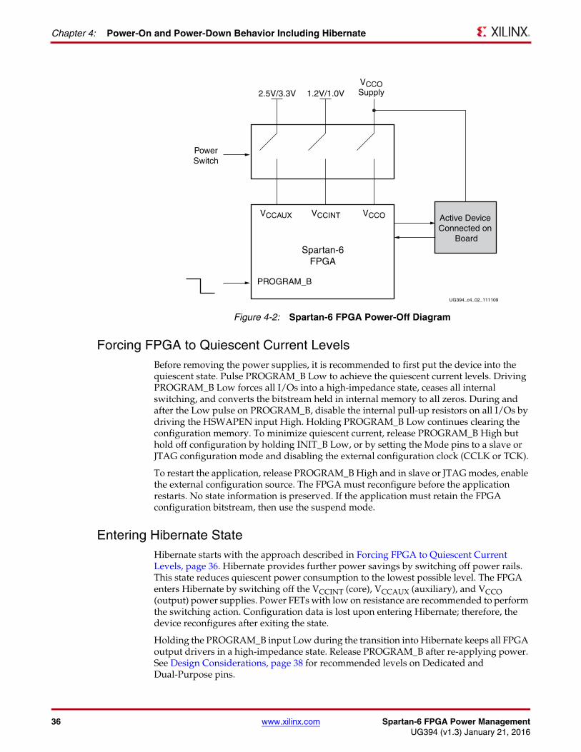
36 www.xilinx.com Spartan-6 FPGA Power ManagementUG394 (v1.3) January 21, 2016
Chapter 4: Power-On and Power-Down Behavior Including Hibernate
Forcing FPGA to Quiescent Current LevelsBefore removing the power supplies, it is recommended to first put the device into the quiescent state. Pulse PROGRAM_B Low to achieve the quiescent current levels. Driving PROGRAM_B Low forces all I/Os into a high-impedance state, ceases all internal switching, and converts the bitstream held in internal memory to all zeros. During and after the Low pulse on PROGRAM_B, disable the internal pull-up resistors on all I/Os by driving the HSWAPEN input High. Holding PROGRAM_B Low continues clearing the configuration memory. To minimize quiescent current, release PROGRAM_B High but hold off configuration by holding INIT_B Low, or by setting the Mode pins to a slave or JTAG configuration mode and disabling the external configuration clock (CCLK or TCK).
To restart the application, release PROGRAM_B High and in slave or JTAG modes, enable the external configuration source. The FPGA must reconfigure before the application restarts. No state information is preserved. If the application must retain the FPGA configuration bitstream, then use the suspend mode.
Entering Hibernate StateHibernate starts with the approach described in Forcing FPGA to Quiescent Current Levels, page 36. Hibernate provides further power savings by switching off power rails. This state reduces quiescent power consumption to the lowest possible level. The FPGA enters Hibernate by switching off the VCCINT (core), VCCAUX (auxiliary), and VCCO (output) power supplies. Power FETs with low on resistance are recommended to perform the switching action. Configuration data is lost upon entering Hibernate; therefore, the device reconfigures after exiting the state.
Holding the PROGRAM_B input Low during the transition into Hibernate keeps all FPGA output drivers in a high-impedance state. Release PROGRAM_B after re-applying power. See Design Considerations, page 38 for recommended levels on Dedicated and Dual-Purpose pins.
X-Ref Target - Figure 4-2
Figure 4-2: Spartan-6 FPGA Power-Off Diagram
VCCAUX
PROGRAM_B
Active Device Connected on
Board
UG394_c4_02_111109
PowerSwitch
2.5V/3.3V 1.2V/1.0V
VCCINT VCCO
VCCOSupply
Spartan-6FPGA
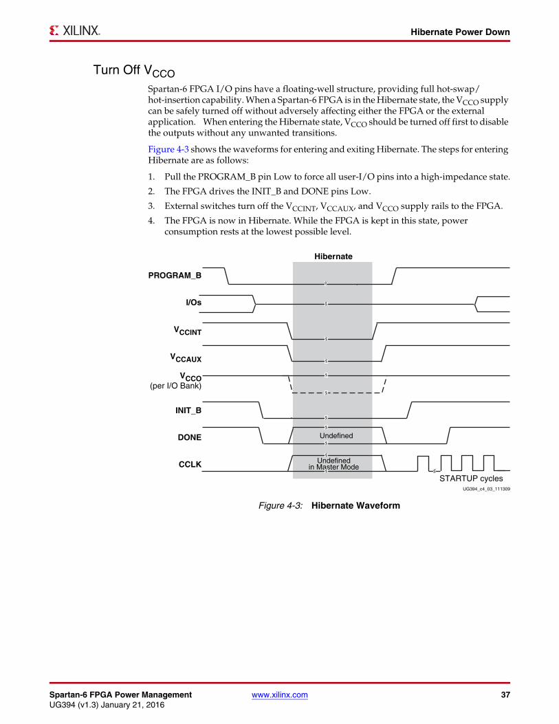
Spartan-6 FPGA Power Management www.xilinx.com 37UG394 (v1.3) January 21, 2016
Hibernate Power Down
Turn Off VCCOSpartan-6 FPGA I/O pins have a floating-well structure, providing full hot-swap/hot-insertion capability. When a Spartan-6 FPGA is in the Hibernate state, the VCCO supply can be safely turned off without adversely affecting either the FPGA or the external application. When entering the Hibernate state, VCCO should be turned off first to disable the outputs without any unwanted transitions.
Figure 4-3 shows the waveforms for entering and exiting Hibernate. The steps for entering Hibernate are as follows:
1. Pull the PROGRAM_B pin Low to force all user-I/O pins into a high-impedance state.
2. The FPGA drives the INIT_B and DONE pins Low.
3. External switches turn off the VCCINT, VCCAUX, and VCCO supply rails to the FPGA.
4. The FPGA is now in Hibernate. While the FPGA is kept in this state, power consumption rests at the lowest possible level.
X-Ref Target - Figure 4-3
Figure 4-3: Hibernate Waveform
PROGRAM_B
I/Os
VCCINT
VCCAUX
VCCO(per I/O Bank)
INIT_B
DONE
CCLK Undefinedin Master Mode
UG394_c4_03_111309
Hibernate
Undefined
STARTUP cycles
38 www.xilinx.com Spartan-6 FPGA Power ManagementUG394 (v1.3) January 21, 2016
Chapter 4: Power-On and Power-Down Behavior Including Hibernate
Exiting HibernateThe steps for exiting Hibernate are as follows.
1. Reapply power to all rails that were switched off. Apply power in any sequence.
2. Before FPGA initialization can begin, deassert PROGRAM_B to a High logic level. The rising transition on PROGRAM_B must occur after turning all three power supplies back on.
3. After logic initialization, the FPGA releases the open-drain INIT_B signal. With INIT_B High, the FPGA starts its configuration process.
4. When configuration is complete, the FPGA enters the Start-up phase, asserts DONE, and enables the I/Os, according to how the BitGen options are set.
5. The FPGA is now ready for user operation.
Design ConsiderationsBe aware of how various pins are powered in the application. Most user-I/O pins, including the dual-purpose configuration pins and the dedicated PROGRAM_B and DONE pins, are powered by a specific VCCO supply input. Dedicated configuration pins such as SUSPEND and the JTAG pins are powered by the VCCAUX supply. If disconnecting power to any of these supplies, consider how that affects FPGA configuration when power is re-applied.
For specific information on configuration pins and their associated power rails, refer to UG380, Spartan-6 FPGA Configuration User Guide.
Spartan-6 FPGA Power Management www.xilinx.com 39UG394 (v1.3) January 21, 2016
Chapter 5
Power Estimation
IntroductionXilinx provides a complete power estimation solution using power estimators and analyzers, power-driven implementation tool algorithms, and a variety of power-related documentation. The Power Advantage page provides access to these tools, documentation, and news:
http://www.xilinx.com/products/technology/power/index.htm
To estimate the total power consumption (quiescent plus dynamic) for a specific design use one of the following tools:
• The XPower Power Estimator spreadsheet provides quick, approximate estimates, and does not require the design’s netlist.
• The XPower Analyzer is delivered with the ISE Design Suite software and uses a netlist as input to provide more accurate estimates.
The XPower Power Estimator (XPE) spreadsheet is a power estimation tool typically used in the pre-design and pre-implementation phases of a project. XPE assists with architecture evaluation and device selection, and helps in selecting the appropriate power supply and thermal management components. For comparison and analysis, the XPE spreadsheet for the Spartan-6 family also includes the Extended Spartan-3A family.
XPE considers the resource usage, toggle rates, I/O loading, and many other design factors. Combined with device models, the estimated power distribution can be calculated in XPE. The device models are extracted from measurements, simulation, and/or extrapolation.
After implementation, the XPower Analyzer (XPA) tool (available in the ISE Design Suite software) is used for more accurate estimates and power analysis. For more information about XPA, see the XPower Analyzer Help.
Voltage RegulatorsThe choice of a voltage regulator depends on system requirements and the estimated power consumption requirements for the FPGA. Use the XPower tools to calculate the requirements for a specific device and design. Then choose a regulator from a pin-compatible family so the current capability can be adjusted up or down. External power FETs are easy to upgrade. A soft-start feature that controls output ramp time is useful.
With care, use of overcurrent protection is possible, such as foldback or fuses. Be aware that capacitors are charging at power-on and might draw a significant amount of current for a short time.
40 www.xilinx.com Spartan-6 FPGA Power ManagementUG394 (v1.3) January 21, 2016
Chapter 5: Power Estimation
If necessary, slow the supply voltage ramp to control the charge current. If foldback is not a design requirement, it is best to avoid it, keeping the power-supply design simple.
Various power-supply manufacturers offer complete power solutions for Xilinx FPGAs including some with integrated three-rail regulators specifically designed for Xilinx FPGAs.
Saving PowerLower-power consumption not only reduces power supply requirements but also reduces heat, which increases reliability, allows for smaller form factor packaging, and helps eliminate heat sinks and fans. Spartan-6 FPGAs are designed to minimize power consumption without sacrificing high performance and low cost.
The lowest power state is the quiescent state with no inputs toggling, all outputs disabled, and no pull-up or pull-down resistors in use. This static power state is often dominated by transistor leakage current, which can increase at smaller process geometries. Xilinx has made major advances in the design of the 45 nm Spartan-6 devices. Comparing Spartan-6 FPGAs to Spartan-3A FPGAs, the average static power in Spartan-6 devices is lower. Quiescent current levels are specified in DS162, Spartan-6 FPGA Data Sheet: DC and Switching Characteristics. The lower-power Spartan-6 LX devices offer the lowest quiescent current.
Dynamic (active) power is a function of capacitance, voltage, and frequency (CV2f). In general, capacitance decreases as transistors shrink. But smaller transistors allow users to take advantage of more of them per device, while using faster switching rates, which can lead to increases in dynamic power. Dynamic power consumption can be reduced by reducing the number or frequency of nodes and I/O toggling in a design. Consider the following techniques to eliminate any unnecessary switching in a design and reduce dynamic power:
• Bring all incoming signals to a static state
• Apply rail-to-rail levels to inputs wherever possible
• Turn off as many outputs as possible
• Assign signal standards with small swings to outputs
• Use lower output drive and slower slew rates
• Tie all unused inputs to VCCO or GND outside the device
• Avoid instantiating pull-up and pull-down resistors on I/Os
• Reduce the total length of heavy loaded signals to reduce capacitance
• Disable as many internal oscillating circuits as possible
• Have block RAMs operate in NOCHANGE mode to reduce toggling of the outputs of the block RAM
Spartan-6 FPGA Power Management www.xilinx.com 41UG394 (v1.3) January 21, 2016
ISE Design Suite Power Optimization
Saving Clock Routing PowerClocks are a significant aspect of power consumption because of their high fanout nets and also because controlling them limits the number of logic primitives toggling in a design. If possible, stop the clock where it enters the FPGA, so that it does not consume any FPGA power. If the clock can not be gated externally, then disable it inside the FPGA using the BUFGCE primitive. Avoid using logic to gate clocks, since CLB logic introduces route-dependent skew and makes the design sensitive to the timing hazards of lot-to-lot variations. Minimizing the amount of routing a clock net uses is helpful, since the Xilinx software automatically disables clock nets where possible for unused areas of CLBs.
If possible, minimize the number of DCMs or PLLs required in the design. A single PLL can be shared with both halves of a GTP_DUAL transceiver. A DCM_CLKGEN can be used to dynamically scale clock frequency as needed for the application, helping to minimize power.
ISE Design Suite Power OptimizationPower can also be reduced automatically in the Xilinx design tools. With goal-based implementation, the ISE Design Suite offers a simple, one-step process to specify power optimization. Design Goals and Strategies control the implementation tools by using preset process properties designed to achieve a particular design goal. Power optimization attempts to meet timing constraints as well as reduce power consumption.
For guidelines on design techniques to reduce power consumption, see the Power Advantage page at:
http://www.xilinx.com/products/technology/power/index.htm
42 www.xilinx.com Spartan-6 FPGA Power ManagementUG394 (v1.3) January 21, 2016
Chapter 5: Power Estimation