Embed Size (px)
Citation preview

— OBSOLETE — OBSOLETE — OBSOLETE — OBSOLETE —
This document includes all four modules of the Spartan®-IIE FPGA data sheet.
Module 1: Introduction and Ordering InformationDS077-1 (v3.0) August 9, 2013
• Introduction • Features • General Overview • Product Availability • User I/O Chart • Ordering Information
Module 2: Functional DescriptionDS077-2 (v3.0) August 9, 2013
• Architectural Description- Spartan-IIE Array- Input/Output Block- Configurable Logic Block- Block RAM- Clock Distribution: Delay-Locked Loop- Boundary Scan
• Development System• Configuration
Module 3: DC and Switching CharacteristicsDS077-3 (v3.0) August 9, 2013
• DC Specifications - Absolute Maximum Ratings - Recommended Operating Conditions - DC Characteristics- Power-On Requirements- DC Input and Output Levels
• Switching Characteristics - Pin-to-Pin Parameters- IOB Switching Characteristics- Clock Distribution Characteristics- DLL Timing Parameters- CLB Switching Characteristics- Block RAM Switching Characteristics- TBUF Switching Characteristics- JTAG Switching Characteristics- Configuration Switching Characteristics
Module 4: Pinout TablesDS077-4 (v3.0) August 9, 2013
• Pin Definitions • Pinout Tables
IMPORTANT NOTE: The Spartan-IIE FPGA data sheet is in four modules. Each module has its own Revision History at the end. Use the PDF "Bookmarks" for easy navigation in this volume.
0Spartan-IIE FPGA Family Data Sheet
DS077 August 9, 2013 0 0 Product Specification
R
DS077 August 9, 2013 www.xilinx.com 1Product Specification
© 2001–2013 Xilinx, Inc. All rights reserved. XILINX, the Xilinx logo, the Brand Window, and other designated brands included herein are trademarks of Xilinx, Inc. All other trademarks are the property of their respective owners.

R
— OBSOLETE — OBSOLETE — OBSOLETE — OBSOLETE —
2 www.xilinx.com DS077 August 9, 2013Product Specification
— OBSOLETE — OBSOLETE — OBSOLETE — OBSOLETE —
IntroductionThe Spartan®-IIE Field-Programmable Gate Array family gives users high performance, abundant logic resources, and a rich feature set, all at an exceptionally low price. The seven-member family offers densities ranging from 50,000 to 600,000 system gates, as shown in Table 1. System per-formance is supported beyond 200 MHz.
Features include block RAM (to 288K bits), distributed RAM (to 221,184 bits), 19 selectable I/O standards, and four DLLs (Delay-Locked Loops). Fast, predictable interconnect means that successive design iterations continue to meet timing requirements.
The Spartan-IIE family is a superior alternative to mask-programmed ASICs. The FPGA avoids the initial cost, lengthy development cycles, and inherent risk of conventional ASICs. Also, FPGA programmability permits design upgrades in the field with no hardware replacement necessary (impossible with ASICs).
Features• Second generation ASIC replacement technology
- Densities as high as 15,552 logic cells with up to 600,000 system gates
- Streamlined features based on Virtex®-E FPGA architecture
- Unlimited in-system reprogrammability- Very low cost- Cost-effective 0.15 micron technology
• System level features- SelectRAM™ hierarchical memory:
· 16 bits/LUT distributed RAM· Configurable 4K-bit true dual-port block RAM
· Fast interfaces to external RAM- Fully 3.3V PCI compliant to 64 bits at 66 MHz and
CardBus compliant- Low-power segmented routing architecture- Dedicated carry logic for high-speed arithmetic- Efficient multiplier support- Cascade chain for wide-input functions- Abundant registers/latches with enable, set, reset- Four dedicated DLLs for advanced clock control
· Eliminate clock distribution delay· Multiply, divide, or phase shift
- Four primary low-skew global clock distribution nets- IEEE 1149.1 compatible boundary scan logic
• Versatile I/O and packaging- Pb-free package options- Low-cost packages available in all densities- Family footprint compatibility in common packages- 19 high-performance interface standards
· LVTTL, LVCMOS, HSTL, SSTL, AGP, CTT, GTL· LVDS and LVPECL differential I/O
- Up to 205 differential I/O pairs that can be input, output, or bidirectional
- Hot swap I/O (CompactPCI friendly)• Core logic powered at 1.8V and I/Os powered at 1.5V,
2.5V, or 3.3V
• Fully supported by powerful Xilinx® ISE® development system- Fully automatic mapping, placement, and routing- Integrated with design entry and verification tools- Extensive IP library including DSP functions and
soft processors
Spartan-IIE FPGA Family: Introduction and Ordering Information
DS077-1 (v3.0) August 9, 2013 0 Product Specification
R
Table 1: Spartan-IIE FPGA Family Members
DeviceLogic Cells
Typical System Gate Range
(Logic and RAM)
CLB Array (R x C)
Total CLBs
Maximum Available User I/O(1)
Maximum Differential
I/O Pairs Distributed RAM Bits
Block RAM Bits
XC2S50E 1,728 23,000 - 50,000 16 x 24 384 182 83 24,576 32K
XC2S100E 2,700 37,000 - 100,000 20 x 30 600 202 86 38,400 40K
XC2S150E 3,888 52,000 - 150,000 24 x 36 864 265 114 55,296 48K
XC2S200E 5,292 71,000 - 200,000 28 x 42 1,176 289 120 75,264 56K
XC2S300E 6,912 93,000 - 300,000 32 x 48 1,536 329 120 98,304 64K
XC2S400E 10,800 145,000 - 400,000 40 x 60 2,400 410 172 153,600 160K
XC2S600E 15,552 210,000 - 600,000 48 x 72 3,456 514 205 221,184 288K
Notes: 1. User I/O counts include the four global clock/user input pins. See details in Table 2, page 5
DS077-1 (v3.0) August 9, 2013 www.xilinx.com 3Product Specification
© 2001–2013 Xilinx, Inc. All rights reserved. XILINX, the Xilinx logo, the Brand Window, and other designated brands included herein are trademarks of Xilinx, Inc. All other trademarks are the property of their respective owners.

Spartan-IIE FPGA Family: Introduction and Ordering InformationR
— OBSOLETE — OBSOLETE — OBSOLETE — OBSOLETE —
General OverviewThe Spartan-IIE family of FPGAs have a regular, flexible, programmable architecture of Configurable Logic Blocks (CLBs), surrounded by a perimeter of programmable Input/Output Blocks (IOBs). There are four Delay-Locked Loops (DLLs), one at each corner of the die. Two columns of block RAM lie on opposite sides of the die, between the CLBs and the IOB columns. The XC2S400E has four col-umns and the XC2S600E has six columns of block RAM. These functional elements are interconnected by a powerful hierarchy of versatile routing channels (see Figure 1).
Spartan-IIE FPGAs are customized by loading configura-tion data into internal static memory cells. Unlimited repro-gramming cycles are possible with this approach. Stored values in these cells determine logic functions and intercon-nections implemented in the FPGA. Configuration data can be read from an external serial PROM (master serial mode), or written into the FPGA in slave serial, slave parallel, or Boundary Scan modes. Xilinx offers multiple types of low-cost configuration solutions including the Platform Flash in-system programmable configuration PROMs.
Spartan-IIE FPGAs are typically used in high-volume appli-cations where the versatility of a fast programmable solution adds benefits. Spartan-IIE FPGAs are ideal for shortening product development cycles while offering a cost-effective solution for high volume production.
Spartan-IIE FPGAs achieve high-performance, low-cost operation through advanced architecture and semiconduc-tor technology. Spartan-IIE devices provide system clock rates beyond 200 MHz. In addition to the conventional ben-efits of high-volume programmable logic solutions, Spar-tan-IIE FPGAs also offer on-chip synchronous single-port and dual-port RAM (block and distributed form), DLL clock drivers, programmable set and reset on all flip-flops, fast carry logic, and many other features.
Spartan-IIE Family Compared to Spartan-II Family• Higher density and more I/O• Higher performance• Unique pinouts in cost-effective packages• Differential signaling
- LVDS, Bus LVDS, LVPECL• VCCINT = 1.8V
- Lower power- 5V tolerance with external resistor- 3V tolerance directly
• PCI, LVTTL, and LVCMOS2 input buffers powered by VCCO instead of VCCINT
• Unique larger bitstream
Figure 1: Basic Spartan-IIE Family FPGA Block Diagram
DLL DLL
DLLDLL
BLO
CK
RA
MB
LOC
K R
AM
BLO
CK
RA
MB
LOC
K R
AM
I/O LOGIC
CLBs CLBs
CLBs CLBs
DS077_01_052102
4 www.xilinx.com DS077-1 (v3.0) August 9, 2013Product Specification

Spartan-IIE FPGA Family: Introduction and Ordering InformationR
— OBSOLETE — OBSOLETE — OBSOLETE — OBSOLETE —
Spartan-IIE Product AvailabilityTable 2 shows the maximum user I/Os available on the device and the number of user I/Os available for each device/package combination.
Table 2: Spartan-IIE FPGA User I/O Chart
DeviceMaximum User I/O
Available User I/O According to Package Type
TQ144TQG144
PQ208PQG208
FT256FTG256
FG456FGG456
FG676FGG676
XC2S50E 182 102 146 182 - -
XC2S100E 202 102 146 182 202 -
XC2S150E 265 - 146 182 265 -
XC2S200E 289 - 146 182 289 -
XC2S300E 329 - 146 182 329 -
XC2S400E 410 - - 182 329 410
XC2S600E 514 - - - 329 514
Notes: 1. User I/O counts include the four global clock/user input pins.
DS077-1 (v3.0) August 9, 2013 www.xilinx.com 5Product Specification

Spartan-IIE FPGA Family: Introduction and Ordering InformationR
— OBSOLETE — OBSOLETE — OBSOLETE — OBSOLETE —
Ordering InformationSpartan-IIE devices are available in both standard and Pb-free packaging options for all device/package combinations. The Pb-free packages include a special "G" character in the ordering code.
Standard Packaging
Pb-Free Packaging
Device Part MarkingFigure 2 is a top marking example for Spartan-IIE FPGAs in the quad-flat packages. The markings for BGA packages are nearly identical to those for the quad-flat packages, except that the marking is rotated with respect to the ball A1 indicator.
The "7C" and "6I" Speed Grade/Temperature Range part combinations may be dual marked as "7C/6I". Devices with the dual mark can be used as either -7C or -6I devices. Devices with a single mark are only guaranteed for the marked speed grade and temperature range.
XC2S50E -6 PQ 208 C
Device Type
Speed Grade
Temperature Range
Package Type
Number of Pins
Example:
DS077-1_03a_072004
XC2S50E -6 PQ 208 C
Device Type
Speed Grade
Temperature Range
Package Type
Number of Pins
Pb-free
GExample:
DS077-1_03b_072004
Device Ordering Options
Device Speed Grade Package Type / Number of Pins Temperature Range ( TJ )(2)
XC2S50E -6 Standard Performance TQ(G)144 144-pin Plastic Thin QFP C = Commercial 0°C to + 85°C
XC2S100E -7 Higher Performance(1) PQ(G)208 208-pin Plastic QFP I = Industrial – 40°C to +100°C
XC2S150E FT(G)256 256-ball Fine Pitch BGA
XC2S200E FG(G)456 456-ball Fine Pitch BGA
XC2S300E FG(G)676 676-ball Fine Pitch BGA
XC2S400E
XC2S600E
Notes: 1. The -7 speed grade is exclusively available in the Commercial temperature range.2. See www.xilinx.com for information on automotive temperature range devices.
Figure 2: Spartan-IIE QFP Marking Example
Lot Code (numeric)
Date Code
Sample package with part markingfor XC2S50E-6PQ208C.
XC2S50EPQ208xxx0425xxxxxxxxx6C
SPARTAN
Device Type
Package
Speed
Operating Range
R
R
ds077-1_02_072804
6 www.xilinx.com DS077-1 (v3.0) August 9, 2013Product Specification

Spartan-IIE FPGA Family: Introduction and Ordering InformationR
— OBSOLETE — OBSOLETE — OBSOLETE — OBSOLETE —
Revision History
Date Version Description
06/27/2002 1.1 Updated -7 availability.
11/18/2002 2.0 Added XC2S400E and XC2S600E. Corrected XC2S150E max I/O count and XC2S50E differential I/O count and updated availability.
07/09/2003 2.1 Noted hot-swap capability. Updated Table 2 to show that all products are available. Clarified device part marking.
07/28/2004 2.2 Added information on Pb-free packaging options.
06/18/2008 2.3 Added dual mark information in Device Part Marking. Updated all modules for continuous page, figure, and table numbering. Updated links. Synchronized all modules to v2.3.
08/09/2013 3.0 This product is obsolete/discontinued per XCN12026.
DS077-1 (v3.0) August 9, 2013 www.xilinx.com 7Product Specification
Spartan-IIE FPGA Family: Introduction and Ordering InformationR
— OBSOLETE — OBSOLETE — OBSOLETE — OBSOLETE —
8 www.xilinx.com DS077-1 (v3.0) August 9, 2013Product Specification

— OBSOLETE — OBSOLETE — OBSOLETE — OBSOLETE —
Architectural Description
Spartan-IIE FPGA ArrayThe Spartan®-IIE user-programmable gate array, shown in Figure 3, is composed of five major configurable elements:
• IOBs provide the interface between the package pins and the internal logic
• CLBs provide the functional elements for constructing most logic
• Dedicated block RAM memories of 4096 bits each• Clock DLLs for clock-distribution delay compensation
and clock domain control• Versatile multi-level interconnect structure
As can be seen in Figure 3, the CLBs form the central logic structure with easy access to all support and routing struc-tures. The IOBs are located around all the logic and mem-ory elements for easy and quick routing of signals on and off the chip.
Values stored in static memory cells control all the configu-rable logic elements and interconnect resources. These val-ues load into the memory cells on power-up, and can reload if necessary to change the function of the device.
Each of these elements will be discussed in detail in the fol-lowing sections.
Spartan-IIE FPGA Family:Functional Description
DS077-2 (v3.0) August 9, 2013 0 Product Specification
R
Figure 3: Basic Spartan-IIE Family FPGA Block Diagram
DLL DLL
DLLDLL
BLO
CK
RA
MB
LOC
K R
AM
BLO
CK
RA
MB
LOC
K R
AM
I/O LOGIC
CLBs CLBs
CLBs CLBs
DS077_01_052102
DS077-2 (v3.0) August 9, 2013 www.xilinx.com 9Product Specification
© 2001-2013 Xilinx, Inc. All rights reserved. XILINX, the Xilinx logo, the Brand Window, and other designated brands included herein are trademarks of Xilinx, Inc. All other trademarks are the property of their respective owners.

Spartan-IIE FPGA Family: Functional DescriptionR
— OBSOLETE — OBSOLETE — OBSOLETE — OBSOLETE —
Input/Output BlockThe Spartan-IIE FPGA IOB, as seen in Figure 4, features inputs and outputs that support a wide variety of I/O signal-ing standards. These high-speed inputs and outputs are capable of supporting various state of the art memory and bus interfaces. The default standard is LVTTL. Table 3 lists several of the standards which are supported along with the required reference (VREF), output (VCCO) and board termi-nation (VTT) voltages needed to meet the standard. For more details on the I/O standards and termination applica-tion examples, see XAPP179, "Using SelectIO Interfaces in Spartan-II and Spartan-IIE FPGAs."
The three IOB registers function either as edge-triggered D-type flip-flops or as level-sensitive latches. Each IOB has a clock signal (CLK) shared by the three registers and inde-pendent Clock Enable (CE) signals for each register.
In addition to the CLK and CE control signals, the three reg-isters share a Set/Reset (SR). For each register, this signal can be independently configured as a synchronous Set, a synchronous Reset, an asynchronous Preset, or an asyn-chronous Clear.
A feature not shown in the block diagram, but controlled by the software, is polarity control. The input and output buffers and all of the IOB control signals have independent polarity controls.
Figure 4: Spartan-IIE Input/Output Block (IOB)
Package Pin
PackagePin
Package Pin
D
CK
EC
SRQ
D
CK
EC
SRQ
D
CK
EC
SRQ
ProgrammableBias and
ESD Network
VCCO
I/O
I/O, VREF
InternalReference
To Next I/OTo Other
External VREF Inputsof BankNotes:
1. For some I/O standards.
ProgrammableInput Buffer
ProgrammableOutput Buffer
ProgrammableDelay
VCC
VCC(1)
OE
SR
O
OCE
I
ICE
IQ
CLK
TCE
T
DS077-2_01_051501
TFF
OFF
IFF
Table 3: Standards Supported by I/O (Typical Values)
I/O Standard
Input Reference
Voltage (VREF)
Input Voltage (VCCO)
Output Source Voltage (VCCO)
Board Termination
Voltage (VTT)
LVTTL (2-24 mA) N/A 3.3 3.3 N/A
LVCMOS2 N/A 2.5 2.5 N/A
LVCMOS18 N/A 1.8 1.8 N/A
PCI (3V, 33 MHz/66 MHz)
N/A 3.3 3.3 N/A
GTL 0.8 N/A N/A 1.2
GTL+ 1.0 N/A N/A 1.5
HSTL Class I 0.75 N/A 1.5 0.75
HSTL Class III 0.9 N/A 1.5 1.5
HSTL Class IV 0.9 N/A 1.5 1.5
SSTL3 Class I and II
1.5 N/A 3.3 1.5
SSTL2 Class I and II
1.25 N/A 2.5 1.25
CTT 1.5 N/A 3.3 1.5
AGP 1.32 N/A 3.3 N/A
LVDS, Bus LVDS N/A N/A 2.5 N/A
LVPECL N/A N/A 3.3 N/A
10 www.xilinx.com DS077-2 (v3.0) August 9, 2013Product Specification
Spartan-IIE FPGA Family: Functional DescriptionR
— OBSOLETE — OBSOLETE — OBSOLETE — OBSOLETE —
Optional pull-up and pull-down resistors and an optional weak-keeper circuit are attached to each user I/O pad. Prior to configuration all outputs not involved in configuration are forced into their high-impedance state. The pull-down resis-tors and the weak-keeper circuits are inactive, but inputs may optionally be pulled up. The activation of pull-up resis-tors prior to configuration is controlled on a global basis by the configuration mode pins. If the pull-up resistors are not activated, all the pins will float. Consequently, external pull-up or pull-down resistors must be provided on pins required to be at a well-defined logic level prior to configura-tion.
All pads are protected against damage from electrostatic discharge (ESD) and from over-voltage transients. After configuration, clamping diodes are connected to VCCO for LVTTL, PCI, HSTL, SSTL, CTT, and AGP standards.
All Spartan-IIE FPGA IOBs support IEEE 1149.1-compati-ble boundary scan testing.
Input PathA buffer in the IOB input path routes the input signal directly to internal logic and through an optional input flip-flop.
An optional delay element at the D-input of this flip-flop elim-inates pad-to-pad hold time. The delay is matched to the internal clock-distribution delay of the FPGA, and when used, assures that the pad-to-pad hold time is zero.
Each input buffer can be configured to conform to any of the low-voltage signaling standards supported. In some of these standards the input buffer utilizes a user-supplied threshold voltage, VREF. The need to supply VREF imposes constraints on which standards can used in close proximity to each other. See I/O Banking.
There are optional pull-up and pull-down resistors at each input for use after configuration.
Output Path
The output path includes a 3-state output buffer that drives the output signal onto the pad. The output signal can be routed to the buffer directly from the internal logic or through an optional IOB output flip-flop.
The 3-state control of the output can also be routed directly from the internal logic or through a flip-flip that provides syn-chronous enable and disable.
Each output driver can be individually programmed for a wide range of low-voltage signaling standards. Each output buffer can source up to 24 mA and sink up to 48 mA. Drive strength and slew rate controls minimize bus transients. The default output driver is LVTTL with 12 mA drive strength and slow slew rate.
In most signaling standards, the output high voltage depends on an externally supplied VCCO voltage. The need to supply VCCO imposes constraints on which standards
can be used in close proximity to each other. See I/O Bank-ing.
An optional weak-keeper circuit is connected to each out-put. When selected, the circuit monitors the voltage on the pad and weakly drives the pin High or Low to match the input signal. If the pin is connected to a multiple-source sig-nal, the weak keeper holds the signal in its last state if all drivers are disabled. Maintaining a valid logic level in this way helps eliminate bus chatter.
Because the weak-keeper circuit uses the IOB input buffer to monitor the input level, an appropriate VREF voltage must be provided if the signaling standard requires one. The pro-vision of this voltage must comply with the I/O banking rules.
I/O BankingSome of the I/O standards described above require VCCOand/or VREF voltages. These voltages are externally sup-plied and connected to device pins that serve groups of IOBs, called banks. Consequently, restrictions exist about which I/O standards can be combined within a given bank.
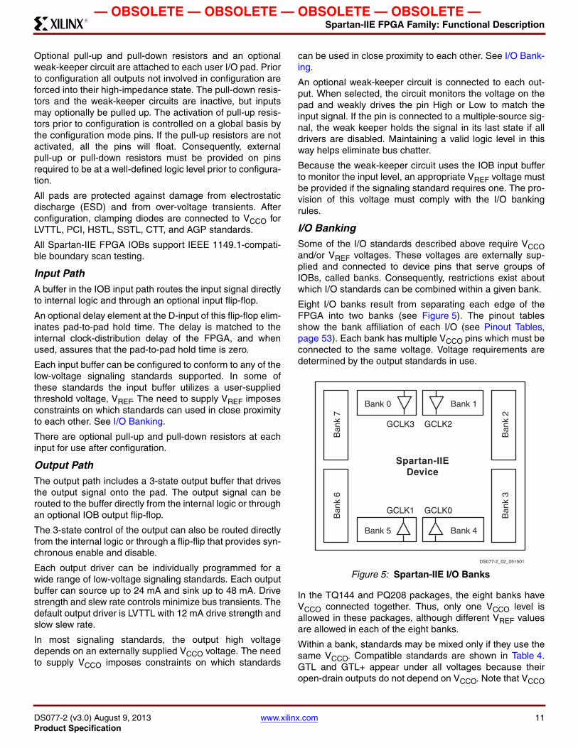
Eight I/O banks result from separating each edge of the FPGA into two banks (see Figure 5). The pinout tables show the bank affiliation of each I/O (see Pinout Tables, page 53). Each bank has multiple VCCO pins which must be connected to the same voltage. Voltage requirements are determined by the output standards in use.
In the TQ144 and PQ208 packages, the eight banks have VCCO connected together. Thus, only one VCCO level is allowed in these packages, although different VREF values are allowed in each of the eight banks.
Within a bank, standards may be mixed only if they use the same VCCO. Compatible standards are shown in Table 4. GTL and GTL+ appear under all voltages because their open-drain outputs do not depend on VCCO. Note that VCCO
Figure 5: Spartan-IIE I/O Banks
DS077-2_02_051501
Bank 0
GCLK3 GCLK2
GCLK1 GCLK0
Bank 1
Bank 5 Bank 4
Spartan-IIEDevice
Ban
k 7
Ban
k 6
Ban
k 2
Ban
k 3
DS077-2 (v3.0) August 9, 2013 www.xilinx.com 11Product Specification
Spartan-IIE FPGA Family: Functional DescriptionR
— OBSOLETE — OBSOLETE — OBSOLETE — OBSOLETE —
is required for most output standards and for LVTTL, LVCMOS, and PCI inputs.
Some input standards require a user-supplied threshold voltage, VREF. In this case, certain user-I/O pins are auto-matically configured as inputs for the VREF voltage. About one in six of the I/O pins in the bank assume this role.
VREF pins within a bank are interconnected internally and consequently only one VREF voltage can be used within each bank. All VREF pins in the bank, however, must be con-nected to the external voltage source for correct operation.
In a bank, inputs requiring VREF can be mixed with those that do not but only one VREF voltage may be used within a bank. The VCCO and VREF pins for each bank appear in the device pinout tables.
Within a given package, the number of VREF and VCCO pins can vary depending on the size of device. In larger devices, more I/O pins convert to VREF pins. Since these are always a superset of the VREF pins used for smaller devices, it is possible to design a PCB that permits migration to a larger device. All VREF pins for the largest device anticipated must be connected to the VREF voltage, and not used for I/O.
See Xilinx® Application Note XAPP179 for more information on I/O resources.
Hot Swap, Hot Insertion, Hot Socketing Support
The I/O pins support hot swap — also called hot insertion and hot socketing — and are considered CompactPCI Friendly according to the PCI Bus v2.2 Specification. Con-sequently, an unpowered Spartan-IIE FPGA can be plugged directly into a powered system or backplane with-out affecting or damaging the system or the FPGA. The hot swap functionality is built into every XC2S150E, XC2S400E, and XC2S600E device. All other Spartan-IIE devices built after Product Change Notice PCN2002-05 also include hot swap functionality.
To support hot swap, Spartan-IIE devices include the follow-ing I/O features.
• Signals can be applied to Spartan-IIE FPGA I/O pins before powering the FPGA’s VCCINT or VCCO supply inputs.
• Spartan-IIE FPGA I/O pins are high-impedance (i.e., three-stated) before and throughout the power-up and configuration processes when employing a configuration mode that does not enable the preconfiguration weak pull-up resistors (see Table 11, page 22).
• There is no current path from the I/O pin back to the VCCINT or VCCO voltage supplies.
• Spartan-IIE FPGAs are immune to latch-up during hot swap.
Once connected to the system, each pin adds a small amount of capacitance (CIN). Likewise, each I/O consumes a small amount of DC current, equivalent to the input leak-age specification (IL). There also may be a small amount of temporary AC current (IHSPO) when the pin input voltage exceeds VCCO plus 0.4V, which lasts less than 10 ns.
A weak-keeper circuit within each user-I/O pin is enabled during the last frame of configuration data and has no noticeable effect on robust system signals driven by an active driver or a strong pull-up or pull-down resistor. Undriven or floating system signals may be affected. The specific effect depends on how the I/O pin is configured. User-I/O pins configured as outputs or enabled outputs have a weak pull-up resistor to VCCO during the last config-uration frame. User-I/O pins configured as inputs or bidirec-tional I/Os have weak pull-down resistors. The weak-keeper circuit turns off when the DONE pin goes High, provided that it is not used in the configured application.
Table 4: Compatible Standards
VCCO Compatible Standards
3.3V PCI, LVTTL, SSTL3 I, SSTL3 II, CTT, AGP, LVPECL, GTL, GTL+
2.5V SSTL2 I, SSTL2 II, LVCMOS2, LVDS, Bus LVDS, GTL, GTL+
1.8V LVCMOS18, GTL, GTL+
1.5V HSTL I, HSTL III, HSTL IV, GTL, GTL+
Table 5: I/O Banking
Package TQ144, PQ208FT256, FG456,
FG676
VCCO Banks Interconnected as 1 8 independent
VREF Banks 8 independent 8 independent
12 www.xilinx.com DS077-2 (v3.0) August 9, 2013Product Specification
Spartan-IIE FPGA Family: Functional DescriptionR
— OBSOLETE — OBSOLETE — OBSOLETE — OBSOLETE —
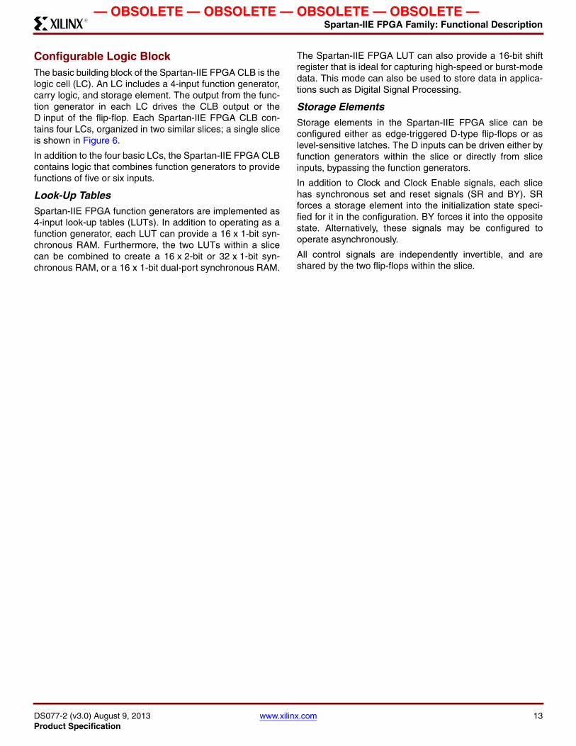
Configurable Logic Block The basic building block of the Spartan-IIE FPGA CLB is the logic cell (LC). An LC includes a 4-input function generator, carry logic, and storage element. The output from the func-tion generator in each LC drives the CLB output or the D input of the flip-flop. Each Spartan-IIE FPGA CLB con-tains four LCs, organized in two similar slices; a single slice is shown in Figure 6.
In addition to the four basic LCs, the Spartan-IIE FPGA CLB contains logic that combines function generators to provide functions of five or six inputs.
Look-Up TablesSpartan-IIE FPGA function generators are implemented as 4-input look-up tables (LUTs). In addition to operating as a function generator, each LUT can provide a 16 x 1-bit syn-chronous RAM. Furthermore, the two LUTs within a slice can be combined to create a 16 x 2-bit or 32 x 1-bit syn-chronous RAM, or a 16 x 1-bit dual-port synchronous RAM.
The Spartan-IIE FPGA LUT can also provide a 16-bit shift register that is ideal for capturing high-speed or burst-mode data. This mode can also be used to store data in applica-tions such as Digital Signal Processing.
Storage Elements
Storage elements in the Spartan-IIE FPGA slice can be configured either as edge-triggered D-type flip-flops or as level-sensitive latches. The D inputs can be driven either by function generators within the slice or directly from slice inputs, bypassing the function generators.
In addition to Clock and Clock Enable signals, each slice has synchronous set and reset signals (SR and BY). SR forces a storage element into the initialization state speci-fied for it in the configuration. BY forces it into the opposite state. Alternatively, these signals may be configured to operate asynchronously.
All control signals are independently invertible, and are shared by the two flip-flops within the slice.
DS077-2 (v3.0) August 9, 2013 www.xilinx.com 13Product Specification

Spartan-IIE FPGA Family: Functional DescriptionR
— OBSOLETE — OBSOLETE — OBSOLETE — OBSOLETE —
Additional Logic
The F5 multiplexer in each slice combines the function gen-erator outputs (Figure 7). This combination provides either a function generator that can implement any 5-input func-tion, a 4:1 multiplexer, or selected functions of up to nine inputs.
Similarly, the F6 multiplexer combines the outputs of all four function generators in the CLB by selecting one of the two F5-multiplexer outputs. This permits the implementation of any 6-input function, an 8:1 multiplexer, or selected func-tions of up to 19 inputs.
Figure 6: Spartan-IIE CLB Slice (two identical slices in each CLB)
I3
I4
I2
I1
Look-UpTable
D
CK
EC
Q
R
S
I3
I4
I2
I1
O
O
Look-UpTable
D
CK
EC
Q
R
SXQ
X
XB
CE
CLK
CIN
BX
F1
F2
F3
SR
BY
F5IN
G1
G2
YQ
Y
YB
COUT
G3
G4
F4
Carryand
ControlLogic
Carryand
ControlLogic
DS001_04_091400
14 www.xilinx.com DS077-2 (v3.0) August 9, 2013Product Specification
Spartan-IIE FPGA Family: Functional DescriptionR
— OBSOLETE — OBSOLETE — OBSOLETE — OBSOLETE —
Each CLB has four direct feedthrough paths, one per LC. These paths provide extra data input lines or additional local routing that does not consume logic resources.
Arithmetic LogicDedicated carry logic provides capability for high-speed arithmetic functions. The Spartan-IIE FPGA CLB supports two separate carry chains, one per slice. The height of the carry chains is two bits per CLB.
The arithmetic logic includes an XOR gate that allows a 1-bit full adder to be implemented within an LC. In addition, a dedicated AND gate improves the efficiency of multiplier implementations.
The dedicated carry path can also be used to cascade func-tion generators for implementing wide logic functions.
BUFTs Each Spartan-IIE FPGA CLB contains two 3-state drivers (BUFTs) that can drive on-chip busses. The IOBs on the left and right sides can also drive the on-chip busses. See Ded-icated Routing, page 17. Each Spartan-IIE FPGA BUFT has an independent 3-state control pin and an independent input pin. The 3-state control pin is an active-Low enable (T). When all BUFTs on a net are disabled, the net is High. There is no need to instantiate a pull-up unless desired for simulation purposes. Simultaneously driving BUFTs onto the same net will not cause contention. If driven both High and Low, the net will be Low.
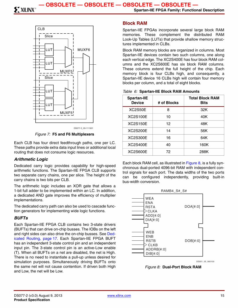
Block RAMSpartan-IIE FPGAs incorporate several large block RAM memories. These complement the distributed RAM Look-Up Tables (LUTs) that provide shallow memory struc-tures implemented in CLBs.
Block RAM memory blocks are organized in columns. Most Spartan-IIE devices contain two such columns, one along each vertical edge. The XC2S400E has four block RAM col-umns and the XC2S600E has six block RAM columns. These columns extend the full height of the chip. Each memory block is four CLBs high, and consequently, a Spartan-IIE device 16 CLBs high will contain four memory blocks per column, and a total of eight blocks.
Each block RAM cell, as illustrated in Figure 8, is a fully syn-chronous dual-ported 4096-bit RAM with independent con-trol signals for each port. The data widths of the two ports can be configured independently, providing built-in bus-width conversion.
Figure 7: F5 and F6 Multiplexers
LUT
DS077-2_05-111501
LUT
MUXF5
MUXF6
LUT
Slice
Slice
CLB
LUT
MUXF5
Table 6: Spartan-IIE Block RAM Amounts
Spartan-IIE Device # of Blocks
Total Block RAM Bits
XC2S50E 8 32K
XC2S100E 10 40K
XC2S150E 12 48K
XC2S200E 14 56K
XC2S300E 16 64K
XC2S400E 40 160K
XC2S600E 72 288K
Figure 8: Dual-Port Block RAM
WEBENBRSTB CLKBADDRB[#:0]DIB[#:0]
WEAENARSTA CLKAADD[#:0]DIA[#:0]
DOA[#:0]
DOB[#:0]
RAMB4_S#_S#
DS001_05_060100
DS077-2 (v3.0) August 9, 2013 www.xilinx.com 15Product Specification

Spartan-IIE FPGA Family: Functional DescriptionR
— OBSOLETE — OBSOLETE — OBSOLETE — OBSOLETE —
Table 7 shows the depth and width aspect ratios for the block RAM.
The Spartan-IIE FPGA block RAM also includes dedicated routing to provide an efficient interface with both CLBs and other block RAMs. See Xilinx Application Note XAPP173 for more information on block RAM.
Programmable Routing It is the longest delay path that limits the speed of any design. Consequently, the Spartan-IIE FPGA routing archi-tecture and its place-and-route software were defined jointly to minimize long-path delays and yield the best system per-formance.
The joint optimization also reduces design compilation times because the architecture is software-friendly. Design cycles are correspondingly reduced due to shorter design iteration times.
The software automatically uses the best available routing based on user timing requirements. The details are pro-vided here for reference.
Local RoutingThe local routing resources, as shown in Figure 9, provide the following three types of connections:
• Interconnections among the LUTs, flip-flops, and General Routing Matrix (GRM), described below.
• Internal CLB feedback paths that provide high-speed connections to LUTs within the same CLB, chaining them together with minimal routing delay
• Direct paths that provide high-speed connections between horizontally adjacent CLBs, eliminating the delay of the GRM
General Purpose RoutingMost Spartan-IIE FPGA signals are routed on the general purpose routing, and consequently, the majority of intercon-nect resources are associated with this level of the routing hierarchy. The general routing resources are located in hor-izontal and vertical routing channels associated with the rows and columns of CLBs. The general-purpose routing resources are listed below.
• Adjacent to each CLB is a General Routing Matrix (GRM). The GRM is the switch matrix through which horizontal and vertical routing resources connect, and is also the means by which the CLB gains access to the general purpose routing.
• 24 single-length lines route GRM signals to adjacent GRMs in each of the four directions.
• 96 buffered Hex lines route GRM signals to other GRMs six blocks away in each one of the four directions. Organized in a staggered pattern, Hex lines may be driven only at their endpoints. Hex-line signals can be accessed either at the endpoints or at the midpoint (three blocks from the source). One third of the Hex lines are bidirectional, while the remaining ones are unidirectional.
• 12 Longlines are buffered, bidirectional wires that distribute signals across the device quickly and efficiently. Vertical Longlines span the full height of the device, and horizontal ones span the full width of the device.
I/O RoutingSpartan-IIE devices have additional routing resources around their periphery that form an interface between the CLB array and the IOBs. This additional routing, called the VersaRing™ routing, facilitates pin-swapping and pin-lock-ing, such that logic redesigns can adapt to existing PCB lay-outs. Time-to-market is reduced, since PCBs and other system components can be manufactured while the logic design is still in progress.
Table 7: Block RAM Port Aspect Ratios
Width Depth ADDR Bus Data Bus
1 4096 ADDR<11:0> DATA<0>
2 2048 ADDR<10:0> DATA<1:0>
4 1024 ADDR<9:0> DATA<3:0>
8 512 ADDR<8:0> DATA<7:0>
16 256 ADDR<7:0> DATA<15:0>
Figure 9: Spartan-IIE Local RoutingDS001_06_032300
CLB
GRM
ToAdjacent
GRMTo AdjacentGRM
DirectConnectionTo AdjacentCLB
To AdjacentGRM
To AdjacentGRM
Direct ConnectionTo Adjacent
CLB
16 www.xilinx.com DS077-2 (v3.0) August 9, 2013Product Specification

Spartan-IIE FPGA Family: Functional DescriptionR
— OBSOLETE — OBSOLETE — OBSOLETE — OBSOLETE —
Dedicated Routing
Some classes of signal require dedicated routing resources to maximize performance. In the Spartan-IIE FPGA archi-tecture, dedicated routing resources are provided for two classes of signal.
• Horizontal routing resources are provided for on-chip 3-state busses. Four partitionable bus lines are provided per CLB row, permitting multiple busses within a row, as shown in Figure 10.
• Two dedicated nets per CLB propagate carry signals vertically to the adjacent CLB.
Global RoutingGlobal Routing resources distribute clocks and other sig-nals with very high fanout throughout the device. Spar-tan-IIE devices include two tiers of global routing resources referred to as primary and secondary global routing resources.
• The primary global routing resources are four dedicated global nets with dedicated input pins that are designed to distribute high-fanout clock signals with minimal skew. Each global clock net can drive all CLB, IOB, and block RAM clock pins. The primary global nets may only be driven by global buffers. There are four global buffers, one for each global net.
• The secondary global routing resources consist of 24 backbone lines, 12 across the top of the chip and 12 across the bottom. From these lines, up to 12 unique signals per column can be distributed via the 12 longlines in the column. These secondary resources are more flexible than the primary resources since they are not restricted to routing only to clock pins.
Clock DistributionThe Spartan-IIE family provides high-speed, low-skew clock distribution through the primary global routing resources described above. A typical clock distribution net is shown in Figure 11.
Four global buffers are provided, two at the top center of the device and two at the bottom center. These drive the four primary global nets that in turn drive any clock pin.
Four dedicated clock pads are provided, one adjacent to each of the global buffers. The input to the global buffer is
selected either from these pads or from signals in the gen-eral purpose routing.
Delay-Locked Loop (DLL)Associated with each global clock input buffer is a fully digi-tal Delay-Locked Loop (DLL) that can eliminate skew between the clock input pad and internal clock-input pins throughout the device. Each DLL can drive two global clock networks. The DLL monitors the input clock and the distrib-uted clock, and automatically adjusts a clock delay element (Figure 12). Additional delay is introduced such that clock edges reach internal flip-flops exactly one clock period after they arrive at the input. This closed-loop system effectively eliminates clock-distribution delay by ensuring that clock
Figure 10: BUFT Connections to Dedicated Horizontal Bus Lines
CLB CLB CLB CLB
3-StateLines
DS001_07_090600
Figure 11: Global Clock Distribution Network
Global Clock Spine
Global Clock Column
GCLKPAD2GCLKBUF2
GCLKPAD3GCLKBUF3
GCLKBUF1GCLKPAD1
GCLKBUF0GCLKPAD0
Global Clock Rows
DS001_08_060100
DS077-2 (v3.0) August 9, 2013 www.xilinx.com 17Product Specification
Spartan-IIE FPGA Family: Functional DescriptionR
— OBSOLETE — OBSOLETE — OBSOLETE — OBSOLETE —
edges arrive at internal flip-flops in synchronism with clock edges arriving at the input.
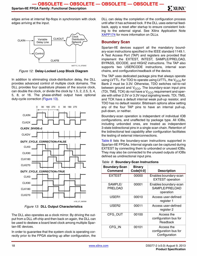
In addition to eliminating clock-distribution delay, the DLL provides advanced control of multiple clock domains. The DLL provides four quadrature phases of the source clock, can double the clock, or divide the clock by 1.5, 2, 2.5, 3, 4, 5, 8, or 16. The phase-shifted output have optional duty-cycle correction (Figure 13).
The DLL also operates as a clock mirror. By driving the out-put from a DLL off-chip and then back on again, the DLL can be used to deskew a board level clock among multiple Spar-tan-IIE devices.
In order to guarantee that the system clock is operating cor-rectly prior to the FPGA starting up after configuration, the
DLL can delay the completion of the configuration process until after it has achieved lock. If the DLL uses external feed-back, apply a reset after startup to ensure consistent lock-ing to the external signal. See Xilinx Application Note XAPP174 for more information on DLLs.
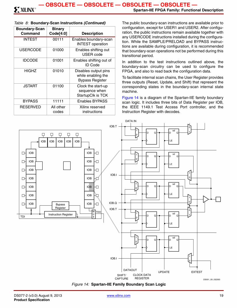
Boundary ScanSpartan-IIE devices support all the mandatory bound-ary-scan instructions specified in the IEEE standard 1149.1. A Test Access Port (TAP) and registers are provided that implement the EXTEST, INTEST, SAMPLE/PRELOAD, BYPASS, IDCODE, and HIGHZ instructions. The TAP also supports two USERCODE instructions, internal scan chains, and configuration/readback of the device.
The TAP uses dedicated package pins that always operate using LVTTL. For TDO to operate using LVTTL, the VCCO for Bank 2 must be 3.3V. Otherwise, TDO switches rail-to-rail between ground and VCCO. The boundary-scan input pins (TDI, TMS, TCK) do not have a VCCO requirement and oper-ate with either 2.5V or 3.3V input signaling levels. TDI, TMS, and TCK hava a default internal weak pull-up resistor, and TDO has no default resistor. Bitstream options allow setting any of the four TAP pins to have an internal pull-up, pull-down, or neither.
Boundary-scan operation is independent of individual IOB configurations, and unaffected by package type. All IOBs, including unbonded ones, are treated as independent 3-state bidirectional pins in a single scan chain. Retention of the bidirectional test capability after configuration facilitates the testing of external interconnections.
Table 8 lists the boundary-scan instructions supported in Spartan-IIE FPGAs. Internal signals can be captured during EXTEST by connecting them to unbonded or unused IOBs. They may also be connected to the unused outputs of IOBs defined as unidirectional input pins.
Figure 12: Delay-Locked Loop Block Diagram
Figure 13: DLL Output Characteristics
ClockDistributionNetwork
VariableDelay Line
CLKOUT
Control
CLKFB
CLKIN
ds077-2_10_070203
x132_07_092599
CLKIN
CLK2X
CLK0
CLK90
CLK180
CLK270
CLKDV
CLKDV_DIVIDE=2
DUTY_CYCLE_CORRECTION=FALSE
CLK0
CLK90
CLK180
CLK270
DUTY_CYCLE_CORRECTION=TRUE
t0 90 180 270 0 90 180 270
Table 8: Boundary-Scan Instructions
Boundary-Scan Command
Binary Code[4:0] Description
EXTEST 00000 Enables boundary-scan EXTEST operation
SAMPLE/PRELOAD
00001 Enables boundary-scan SAMPLE/PRELOAD
operation
USER1 00010 Access user-defined register 1
USER2 00011 Access user-defined register 2
CFG_OUT 00100 Access the configuration bus for
Readback
CFG_IN 00101 Access the configuration bus for
Configuration
18 www.xilinx.com DS077-2 (v3.0) August 9, 2013Product Specification
Spartan-IIE FPGA Family: Functional DescriptionR
— OBSOLETE — OBSOLETE — OBSOLETE — OBSOLETE —
The public boundary-scan instructions are available prior to configuration, except for USER1 and USER2. After configu-ration, the public instructions remain available together with any USERCODE instructions installed during the configura-tion. While the SAMPLE/PRELOAD and BYPASS instruc-tions are available during configuration, it is recommended that boundary-scan operations not be performed during this transitional period.
In addition to the test instructions outlined above, the boundary-scan circuitry can be used to configure the FPGA, and also to read back the configuration data.
To facilitate internal scan chains, the User Register provides three outputs (Reset, Update, and Shift) that represent the corresponding states in the boundary-scan internal state machine.
Figure 14 is a diagram of the Spartan-IIE family boundary scan logic. It includes three bits of Data Register per IOB, the IEEE 1149.1 Test Access Port controller, and the Instruction Register with decodes.
INTEST 00111 Enables boundary-scan INTEST operation
USERCODE 01000 Enables shifting out USER code
IDCODE 01001 Enables shifting out of ID Code
HIGHZ 01010 Disables output pins while enabling the Bypass Register
JSTART 01100 Clock the start-up sequence when
StartupClk is TCK
BYPASS 11111 Enables BYPASS
RESERVED All other codes
Xilinx reserved instructions
Table 8: Boundary-Scan Instructions (Continued)
Boundary-Scan Command
Binary Code[4:0] Description
Figure 14: Spartan-IIE Family Boundary Scan Logic
D Q
D Q
IOB
IOB
IOB
IOB
IOB
IOB
IOB
IOB
IOB
IOB
IOB
IOB
IOB
MUX
BypassRegister
IOB IOB
TDO
TDI
IOB IOB IOB
1
0
1
0
1
0
1
0
1
0sd
LE
D Q
D Q
D Q
1
0
1
0
1
0
1
0
D Q
LE
sd
sd
LE
D Q
sd
LE
D Q
IOB
D Q1
0D Q
LE
sd
IOB.T
DATA IN
IOB.I
IOB.Q
IOB.T
IOB.I
SHIFT/CAPTURE
CLOCK DATAREGISTER
DATAOUTUPDATE EXTEST
DS001_09_032300
Instruction Register
DS077-2 (v3.0) August 9, 2013 www.xilinx.com 19Product Specification

Spartan-IIE FPGA Family: Functional DescriptionR
— OBSOLETE — OBSOLETE — OBSOLETE — OBSOLETE —
Bit Sequence
The bit sequence within each IOB is: In, Out, 3-State. The input-only pins contribute only the In bit to the boundary scan I/O data register, while the output-only pins contributes all three bits.
From a cavity-up view of the chip (as shown in the FPGA Editor), starting in the upper right chip corner, the boundary scan data-register bits are ordered as shown in Figure 15.
BSDL (Boundary Scan Description Language) files for Spartan-IIE family devices are available on the Xilinx web site.
Spartan-IIE FPGA boundary scan IDCODE values are shown in Table 9.
Development SystemSpartan-IIE FPGAs are supported by the Xilinx ISE® CAE tools. The basic methodology for Spartan-IIE FPGA design consists of three interrelated steps: design entry, imple-mentation, and verification. Industry-standard tools are used for design entry and simulation, while Xilinx provides proprietary architecture-specific tools for implementation.
The Xilinx development system is integrated under the Xilinx Project Navigator software, providing designers with a common user interface regardless of their choice of entry and verification tools. The software simplifies the selection of implementation options with pull-down menus and on-line help.
Several advanced software features facilitate Spartan-IIE FPGA design. CORE Generator™ tool functions, for exam-ple, include macros with relative location constraints to guide their placement. They help ensure optimal implemen-tation of common functions.
For HDL design entry, the Xilinx FPGA development system provides interfaces to several synthesis design environ-ments.
A standard interface-file specification, Electronic Design Interchange Format (EDIF), simplifies file transfers into and out of the development system.
Spartan-IIE FPGAs are supported by a unified library of standard functions. This library contains over 400 primitives and macros, ranging from 2-input AND gates to 16-bit accu-mulators, and includes arithmetic functions, comparators, counters, data registers, decoders, encoders, I/O functions, latches, Boolean functions, multiplexers, shift registers, and barrel shifters.
The design environment supports hierarchical design entry, with high-level designs that comprise major functional blocks, while lower-level designs define the logic in these blocks. These hierarchical design elements are automati-cally combined by the implementation tools. Different design entry tools can be combined within a hierarchical
Figure 15: Boundary Scan Bit Sequence
Bit 0 ( TDO end)Bit 1Bit 2
TDO.TTDO.O
Top-edge IOBs (Right to Left)
Left-edge IOBs (Top to Bottom)
MODE.I
Bottom-edge IOBs (Left to Right)
Right-edge IOBs (Bottom to Top)
BSCANT.UPD(TDI end)
DS001_10_032300
Table 9: Spartan-IIE IDCODE Values
Device
IDCODE
Version Family Array Size Manufacturer Required
XC2S50E XXXX 0000 101 0 0001 0000 0000 1001 001 1
XC2S100E XXXX 0000 101 0 0001 0100 0000 1001 001 1
XC2S150E XXXX 0000 101 0 0001 1000 0000 1001 001 1
XC2S200E XXXX 0000 101 0 0001 1100 0000 1001 001 1
XC2S300E XXXX 0000 101 0 0010 0000 0000 1001 001 1
XC2S400E XXXX 0000 101 0 0010 1000 0000 1001 001 1
XC2S600E XXXX 0000 101 0 0011 0000 0000 1001 001 1
20 www.xilinx.com DS077-2 (v3.0) August 9, 2013Product Specification

Spartan-IIE FPGA Family: Functional DescriptionR
— OBSOLETE — OBSOLETE — OBSOLETE — OBSOLETE —
design, thus allowing the most convenient entry method to be used for each portion of the design.
Design ImplementationThe place-and-route tools automatically provide the imple-mentation flow described in this section. The partitioner takes the EDIF netlist for the design and maps the logic into the architectural resources of the FPGA (CLBs and IOBs, for example). The placer then determines the best locations for these blocks based on their interconnections and the desired performance. Finally, the router interconnects the blocks.
The algorithms support fully automatic implementation of most designs. For demanding applications, however, the user can exercise various degrees of control over the pro-cess. User partitioning, placement, and routing information is optionally specified during the design-entry process. The implementation of highly structured designs can benefit greatly from basic floorplanning.
The implementation software incorporates timing-driven placement and routing. Designers specify timing require-ments along entire paths during design entry. The timing path analysis routines then recognize these user-specified requirements and accommodate them.
Timing requirements are entered in a form directly relating to the system requirements, such as the targeted clock fre-quency, or the maximum allowable delay between two reg-isters. In this way, the overall performance of the system along entire signal paths is automatically tailored to user-generated specifications. Specific timing information for individual nets is unnecessary.
Design VerificationIn addition to conventional software simulation, FPGA users can use in-circuit debugging techniques. Because Xilinx devices are infinitely reprogrammable, designs can be veri-fied in real time without the need for extensive sets of soft-ware simulation vectors.
The development system supports both software simulation and in-circuit debugging techniques. For simulation, the system extracts the post-layout timing information from the design database, and back-annotates this information into the netlist for use by the simulator. Alternatively, the user can verify timing-critical portions of the design using the static timing analyzer.
For in-circuit debugging, Xilinx offers a download cable, which connects the FPGA in the target system to a PC or workstation. After downloading the design into the FPGA, the designer can read back the contents of the flip-flops, and so observe the internal logic state. Simple modifica-tions can be downloaded into the system in a matter of min-utes.
ConfigurationConfiguration is the process by which the bitstream of a design, as generated by the Xilinx development software, is loaded into the internal configuration memory of the FPGA. Spartan-IIE devices support both serial configuration, using the master/slave serial and JTAG modes, as well as byte-wide configuration employing the Slave Parallel mode.
Configuration FileSpartan-IIE devices are configured by sequentially loading frames of data that have been concatenated into a configu-ration file. Table 10 shows how much nonvolatile storage space is needed for Spartan-IIE devices.
It is important to note that, while a PROM is commonly used to store configuration data before loading them into the FPGA, it is by no means required. Any of a number of differ-ent kinds of under populated nonvolatile storage already available either on or off the board (for example, hard drives, FLASH cards, and so on) can be used.
ModesSpartan-IIE devices support the following four configuration modes:
• Slave Serial mode• Master Serial mode• Slave Parallel mode• Boundary-scan mode
The Configuration mode pins (M2, M1, M0) select among these configuration modes with the option in each case of having the IOB pins either pulled up or left floating prior to the end of configuration. The selection codes are listed in Table 11.
Configuration through the boundary-scan port is always available, independent of the mode selection. Selecting the boundary-scan mode simply turns off the other modes. The three mode pins have internal pull-up resistors, and default to a logic High if left unconnected.
Table 10: Spartan-IIE Configuration File Size
Device Configuration File Size (Bits)
XC2S50E 630,048
XC2S100E 863,840
XC2S150E 1,134,496
XC2S200E 1,442,016
XC2S300E 1,875,648
XC2S400E 2,693,440
XC2S600E 3,961,632
DS077-2 (v3.0) August 9, 2013 www.xilinx.com 21Product Specification

Spartan-IIE FPGA Family: Functional DescriptionR
— OBSOLETE — OBSOLETE — OBSOLETE — OBSOLETE —
SignalsThere are two kinds of pins that are used to configure Spartan-IIE devices: Dedicated pins perform only specific configuration-related functions; the other pins can serve as general purpose I/Os once user operation has begun.
The dedicated pins comprise the mode pins (M2, M1, M0), the configuration clock pin (CCLK), the PROGRAM pin, the DONE pin and the boundary-scan pins (TDI, TDO, TMS, TCK). Depending on the selected configuration mode, CCLK may be an output generated by the FPGA, or may be generated externally, and provided to the FPGA as an input.
Note that some configuration pins can act as outputs. For correct operation, these pins require a VCCO of 3.3V to drive an LVTTL signal or 2.5V to drive an LVCMOS signal. All the relevant pins fall in banks 2 or 3. The CS and WRITE pins for Slave Parallel mode are located in bank 1.
For a more detailed description than that given below, see Module 1 and XAPP176, Configuration and Readback of the Spartan-II and Spartan-IIE FPGA Families.
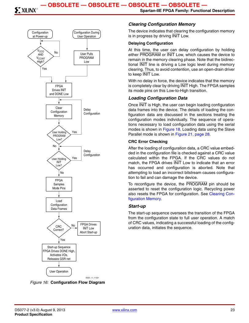
The ProcessThe sequence of steps necessary to configure Spartan-IIE devices are shown in Figure 16. The overall flow can be divided into three different phases.
• Initiating configuration• Configuration memory clear
• Loading data frames• Start-up
The memory clearing and start-up phases are the same for all configuration modes; however, the steps for the loading of data frames are different. Thus, the details for data frame loading are described separately in the sections devoted to each mode.
Initiating ConfigurationThere are two different ways to initiate the configuration pro-cess: applying power to the device or asserting the PRO-GRAM input.
Configuration on power-up occurs automatically unless it is delayed by the user, as described in a separate section below. The waveform for configuration on power-up is shown in Configuration Switching Characteristics, page 48. Before configuration can begin, VCCO Bank 2 must be greater than 1.0V. Furthermore, all VCCINT power pins must be connected to a 1.8V supply. For more information on delaying configuration, see Clearing Configuration Memory, page 23.
Once in user operation, the device can be re-configured simply by pulling the PROGRAM pin Low. The device acknowledges the beginning of the configuration process by driving DONE Low, then enters the memory-clearing phase.
Table 11: Configuration Modes
Configuration ModePreconfiguration
Pull-ups M0 M1 M2CCLK
Direction Data Width Serial DOUT
Master Serial mode No 0 0 0 Out 1 Yes
Yes 0 0 1
Slave Parallel mode (SelectMAP)
Yes 0 1 0 In 8 No
No 0 1 1
Boundary-Scan mode Yes 1 0 0 N/A 1 No
No 1 0 1
Slave Serial mode Yes 1 1 0 In 1 Yes
No 1 1 1
Notes: 1. During power-on and throughout configuration, the I/O drivers will be in a high-impedance state. After configuration, all unused I/Os
(those not assigned signals) will remain in a high-impedance state. Pins used as outputs may pulse High at the end of configuration (see Answer 10504).
2. If the Mode pins are set for preconfiguration pull-ups, those resistors go into effect once the rising edge of INIT samples the Mode pins. They will stay in effect until GTS is released during startup, after which the UnusedPin bitstream generator option will determine whether the unused I/Os have a pull-up, pull-down, or no resistor.
22 www.xilinx.com DS077-2 (v3.0) August 9, 2013Product Specification
Spartan-IIE FPGA Family: Functional DescriptionR
— OBSOLETE — OBSOLETE — OBSOLETE — OBSOLETE —
Clearing Configuration Memory
The device indicates that clearing the configuration memory is in progress by driving INIT Low.
Delaying Configuration
At this time, the user can delay configuration by holding either PROGRAM or INIT Low, which causes the device to remain in the memory clearing phase. Note that the bidirec-tional INIT line is driving a Low logic level during memory clearing. Thus, to avoid contention, use an open-drain driver to keep INIT Low.
With no delay in force, the device indicates that the memory is completely clear by driving INIT High. The FPGA samples its mode pins on this Low-to-High transition.
Loading Configuration DataOnce INIT is High, the user can begin loading configuration data frames into the device. The details of loading the con-figuration data are discussed in the sections treating the configuration modes individually. The sequence of opera-tions necessary to load configuration data using the serial modes is shown in Figure 18. Loading data using the Slave Parallel mode is shown in Figure 21, page 28.
CRC Error Checking
After the loading of configuration data, a CRC value embed-ded in the configuration file is checked against a CRC value calculated within the FPGA. If the CRC values do not match, the FPGA drives INIT Low to indicate that an error has occurred and configuration is aborted. Note that attempting to load an incorrect bitstream causes configura-tion to fail and can damage the device.
To reconfigure the device, the PROGRAM pin should be asserted to reset the configuration logic. Recycling power also resets the FPGA for configuration. See Clearing Con-figuration Memory.
Start-upThe start-up sequence oversees the transition of the FPGA from the configuration state to full user operation. A match of CRC values, indicating a successful loading of the config-uration data, initiates the sequence.
Figure 16: Configuration Flow Diagram
FPGA DrivesINIT Low
Abort Start-up
User HoldingINITLow?
User HoldingPROGRAM
Low?
FPGADrives INIT
and DONE Low
LoadConfigurationData Frames
User Operation
Configurationat Power-up
DS001_11_111501
NoCRCCorrect?
Yes
FPGASamples
Mode Pins
DelayConfiguration
DelayConfiguration
ClearConfiguration
Memory
User PullsPROGRAM
Low
Start-up SequenceFPGA Drives DONE High,
Activates I/Os,Releases GSR net
Yes
No
Yes
No
No
Yes
Configuration DuringUser Operation
VCCOAND
VCCINTHigh?
DS077-2 (v3.0) August 9, 2013 www.xilinx.com 23Product Specification

Spartan-IIE FPGA Family: Functional DescriptionR
— OBSOLETE — OBSOLETE — OBSOLETE — OBSOLETE —
During start-up, the device performs four operations:
1. The assertion of DONE. The failure of DONE to go High may indicate the unsuccessful loading of configuration data.
2. The release of the Global Three State (GTS). This activates all the I/Os to which signals are assigned. The remaining I/Os stay in a high-impedance state with internal weak pull-up resistors present.
3. The release of the Global Set Reset (GSR). This allows all flip-flops to change state.
4. The assertion of Global Write Enable (GWE). This allows all RAMs and flip-flops to change state.
By default, these operations are synchronized to CCLK. The entire start-up sequence lasts eight cycles, called C0-C7, after which the loaded design is fully functional. The four operations can be selected to switch on any CCLK cycle C1-C6 through settings in the Xilinx Development Software. The default timing for start-up is shown in the top half of Figure 17; heavy lines show default settings.
The default Start-up sequence is that one CCLK cycle after DONE goes High, the global 3-state signal (GTS) is released. This permits device outputs to turn on as neces-sary.
One CCLK cycle later, the Global Set/Reset (GSR) and Global Write Enable (GWE) signals are released. This per-mits the internal storage elements to begin changing state in response to the logic and the user clock.
The bottom half of Figure 17 shows another commonly used version of the start-up timing known as Sync-to-DONE. This version makes the GTS, GSR, and GWE events conditional upon the DONE pin going High. This timing is important for a daisy chain of multiple FPGAs in serial mode, since it ensures that all FPGAs go through start-up together, after all their DONE pins have gone High.
Sync-to-DONE timing is selected by setting the GTS, GSR, and GWE cycles to a value of DONE in the configuration options. This causes these signals to transition one clock cycle after DONE externally transitions High.
The sequence can also be paused at any stage until lock has been achieved on any or all DLLs.
Serial ModesThere are two serial configuration modes. In Master Serial mode, the FPGA controls the configuration process by driv-ing CCLK as an output. In Slave Serial mode, the FPGA passively receives CCLK as an input from an external agent (e.g., a microprocessor, CPLD, or second FPGA in master mode) that is controlling the configuration process. In both modes, the FPGA is configured by loading one bit per CCLK cycle. The MSB of each configuration data byte is always written to the DIN pin first.
See Figure 18 for the sequence for loading data into the Spartan-IIE FPGA serially. This is an expansion of the "Load Configuration Data Frames" block in Figure 16, page 23. Note that CS and WRITE are not normally used during serial configuration. To ensure successful loading of the FPGA, do not toggle WRITE with CS Low during serial configuration.
Figure 17: Start-Up Waveforms
Start-up CLK
Default Cycles
Sync to DONE
0 1 2 3 4 5 6 7
0 1
DONE High
2 3 4 5 6 7
Phase
Start-up CLK
Phase
DONE
GTS
GSR
GWE
DS001_13_090600
DONE
GTS
GSR
GWE
24 www.xilinx.com DS077-2 (v3.0) August 9, 2013Product Specification

Spartan-IIE FPGA Family: Functional DescriptionR
— OBSOLETE — OBSOLETE — OBSOLETE — OBSOLETE —
Slave Serial ModeIn Slave Serial mode, the FPGA’s CCLK pin is driven by an external source, allowing the FPGA to be configured from other logic devices such as microprocessors or in a daisy-chain configuration. Figure 19 shows connections for a Master Serial FPGA configuring a Slave Serial FPGA
from a PROM. A Spartan-IIE device in slave serial mode should be connected as shown for the third device from the left. Slave Serial mode is selected by a <11x> on the mode pins (M0, M1, M2). The weak pull-ups on the mode pins make slave serial the default mode if the pins are left uncon-nected.
The serial bitstream must be setup at the DIN input pin a short time before each rising edge of an externally gener-ated CCLK.
Timing for Slave Serial mode is shown in Figure 24, page 49.
Daisy ChainMultiple FPGAs in Slave Serial mode can be daisy-chained for configuration from a single source. After an FPGA is configured, data for the next device is sent to the DOUT pin. Data on the DOUT pin changes on the rising edge of CCLK. Note that DOUT changes on the falling edge of CCLK for some Xilinx families but mixed daisy chains are allowed. Configuration must be delayed until INIT pins of all daisy-chained FPGAs are High. For more information, see Start-up, page 23.
The maximum amount of data that can be sent to the DOUT pin for a serial daisy chain is 220-1 (1,048,575) 32-bit words, or 33,554,400 bits, which is approximately 8 XC2S600E bit-streams. The configuration bitstream of downstream devices is limited to this size.
Figure 18: Loading Serial Mode Configuration Data
No
Yes
End ofConfiguration
Data File?
After INITGoes High
User Load OneConfigurationBit on Next
CCLK Rising Edge
To CRC Check
DS001_14_032300
Notes: 1. If the DriveDone configuration option is not active for any of the FPGAs, pull up DONE with a 330Ω resistor.
Figure 19: Master/Slave Serial Configuration Circuit Diagram
Spartan-IIE(Master Serial)
XilinxPROM
PROGRAM
M2M0 M1
DOUT
CCLK CLK
3.3V
DATA
CE CEO
RESET/OE
DIN
INITDONE
PROGRAM
3.3 K
DS077-2_04_061708
GND GND
VCC
3.3V
VCCO
VCCINT
1.8V3.3V 3.3V 1.8V
Spartan-IIE(Slave)
DONE INIT
PROGRAM
CCLK
DIN DOUT
M2M0 M1
GND
VCCO
VCCINT
DS077-2 (v3.0) August 9, 2013 www.xilinx.com 25Product Specification

Spartan-IIE FPGA Family: Functional DescriptionR
— OBSOLETE — OBSOLETE — OBSOLETE — OBSOLETE —
Master Serial Mode
In Master Serial mode, the CCLK output of the FPGA drives a Xilinx PROM, which feeds a serial stream of configuration data to the FPGA’s DIN input. Figure 19 shows a Master Serial FPGA configuring a Slave Serial FPGA from a PROM. A Spartan-IIE device in Master Serial mode should be connected as shown for the device on the left side. Mas-ter Serial mode is selected by a <00x> on the mode pins (M0, M1, M2). The PROM RESET pin is driven by INIT, and the CE input is driven by DONE. For more information on serial PROMs, see the Xilinx Configuration PROM data sheets at www.xilinx.com.
The interface is identical to the slave serial mode except that an oscillator internal to the FPGA is used to generate the configuration clock (CCLK). Any of a number of different frequencies ranging from 4 to 60 MHz can be set using the ConfigRate option in the Xilinx development software. When selecting a CCLK frequency, ensure that the serial PROM and any daisy-chained FPGAs are fast enough to support the clock rate. On power-up, while the first 60 bytes of the configuration data are being loaded, the CCLK fre-quency is always 2.5 MHz. This frequency is used until the ConfigRate bits, part of the configuration file, have been loaded into the FPGA, at which point the frequency changes to the selected ConfigRate. Unless a different fre-quency is specified in the design, the default ConfigRate is 4 MHz. The frequency of the CCLK signal created by the internal oscillator has a variance of +45%, –30% from the specified value.
The FPGA accepts one bit of configuration data on each ris-ing CCLK edge. After the FPGA has been loaded, the data for the next device in a daisy-chain is presented on the DOUT pin after the rising CCLK edge. The timing for Master Serial mode is shown in Figure 25, page 49.
Slave Parallel Mode (SelectMAP)The Slave Parallel mode, also known as SelectMAP, is the fastest configuration option. Byte-wide data is written into the FPGA on the D0-D7 pins. Note that D0 is the MSB of each byte for configuration. A BUSY flag is provided for con-trolling the flow of data at a clock frequency above 50 MHz.
Figure 20, page 27 shows the connections for two Spartan-IIE devices using the Slave Parallel mode. Slave Parallel mode is selected by a <011> on the mode pins (M0, M1, M2).
The agent controlling configuration is not shown. Typically, a processor, a microcontroller, or CPLD controls the Slave Parallel interface. The controlling agent provides byte-wide configuration data, CCLK, a Chip Select (CS) signal and a Write signal (WRITE). If BUSY is asserted (High) by the FPGA, the data must be held until BUSY goes Low.
After configuration, the pins of the Slave Parallel port (D0-D7) can be used as additional user I/O. Alternatively, the port may be retained to permit high-speed 8-bit read-back. Then data can be read by deasserting WRITE. If retention is selected, prohibit the D0-D7 pins from being used as user I/O. See Readback, page 28.
26 www.xilinx.com DS077-2 (v3.0) August 9, 2013Product Specification

Spartan-IIE FPGA Family: Functional DescriptionR
— OBSOLETE — OBSOLETE — OBSOLETE — OBSOLETE —
Multiple Spartan-IIE FPGAs can be configured using the Slave Parallel mode, and be made to start-up simultane-ously. To configure multiple devices in this way, wire the indi-vidual CCLK, Data, WRITE, and BUSY pins of all the devices in parallel. The individual devices are loaded sepa-rately by asserting the CS pin of each device in turn and writing the appropriate data. Sync-to-DONE start-up timing is used to ensure that the start-up sequence does not begin until all the FPGAs have been loaded. See Start-up, page 23.
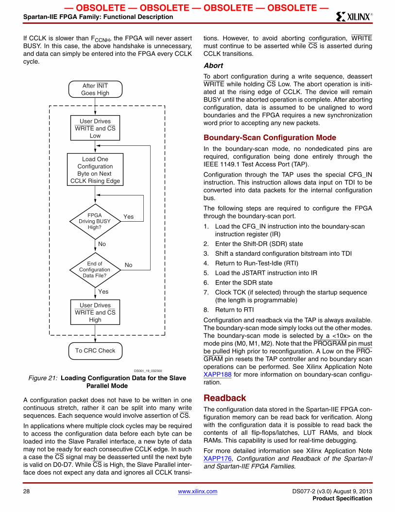
WriteWhen using the Slave Parallel Mode, write operations send packets of byte-wide configuration data into the FPGA. Figure 21, page 28 shows a flowchart of the write sequence used to load data into the Spartan-IIE FPGA. This is an expansion of the "Load Configuration Data Frames" block in Figure 16, page 23.
The timing for Slave Parallel mode is shown in Figure 26, page 50.
For the present example, the user holds WRITE and CSLow throughout the sequence of write operations. Note that when CS is asserted on successive CCLKs, WRITE must remain either asserted or deasserted. Otherwise an abort will be initiated, as in the next section.
1. Drive data onto D0-D7. Note that to avoid contention, the data source should not be enabled while CS is Low and WRITE is High. Similarly, while WRITE is High, no more than one device’s CS should be asserted.
2. On the rising edge of CCLK: If BUSY is Low, the data is accepted on this clock. If BUSY is High (from a previous write), the data is not accepted. Acceptance will instead occur on the first clock after BUSY goes Low, and the data must be held until this happens.
3. Repeat steps 1 and 2 until all the data has been sent.
4. Deassert CS and WRITE.
Figure 20: Slave Parallel Configuration Circuit Diagram
M1 M2
M0
D0:D7
CCLK
WRITE
BUSY
CS
PROGRAM
DONE INIT
CCLK
DATA[7:0]
WRITE
BUSY
CS(0)
Spartan-IIE
DONE
INIT
PROGRAM
M1 M2
M0
D0:D7
CCLK
WRITE
BUSY
CS
PROGRAM
DONE INIT
CS(1)
Spartan-IIE
DS077-2_06_110102
GND GND
DS077-2 (v3.0) August 9, 2013 www.xilinx.com 27Product Specification
Spartan-IIE FPGA Family: Functional DescriptionR
— OBSOLETE — OBSOLETE — OBSOLETE — OBSOLETE —
If CCLK is slower than FCCNH, the FPGA will never assert BUSY. In this case, the above handshake is unnecessary, and data can simply be entered into the FPGA every CCLK cycle.
A configuration packet does not have to be written in one continuous stretch, rather it can be split into many write sequences. Each sequence would involve assertion of CS.
In applications where multiple clock cycles may be required to access the configuration data before each byte can be loaded into the Slave Parallel interface, a new byte of data may not be ready for each consecutive CCLK edge. In such a case the CS signal may be deasserted until the next byte is valid on D0-D7. While CS is High, the Slave Parallel inter-face does not expect any data and ignores all CCLK transi-
tions. However, to avoid aborting configuration, WRITEmust continue to be asserted while CS is asserted during CCLK transitions.
Abort
To abort configuration during a write sequence, deassert WRITE while holding CS Low. The abort operation is initi-ated at the rising edge of CCLK. The device will remain BUSY until the aborted operation is complete. After aborting configuration, data is assumed to be unaligned to word boundaries and the FPGA requires a new synchronization word prior to accepting any new packets.
Boundary-Scan Configuration ModeIn the boundary-scan mode, no nondedicated pins are required, configuration being done entirely through the IEEE 1149.1 Test Access Port (TAP).
Configuration through the TAP uses the special CFG_IN instruction. This instruction allows data input on TDI to be converted into data packets for the internal configuration bus.
The following steps are required to configure the FPGA through the boundary-scan port.
1. Load the CFG_IN instruction into the boundary-scan instruction register (IR)
2. Enter the Shift-DR (SDR) state
3. Shift a standard configuration bitstream into TDI
4. Return to Run-Test-Idle (RTI)
5. Load the JSTART instruction into IR
6. Enter the SDR state
7. Clock TCK (if selected) through the startup sequence (the length is programmable)
8. Return to RTI
Configuration and readback via the TAP is always available. The boundary-scan mode simply locks out the other modes. The boundary-scan mode is selected by a <10x> on the mode pins (M0, M1, M2). Note that the PROGRAM pin must be pulled High prior to reconfiguration. A Low on the PRO-GRAM pin resets the TAP controller and no boundary scan operations can be performed. See Xilinx Application Note XAPP188 for more information on boundary-scan configu-ration.
ReadbackThe configuration data stored in the Spartan-IIE FPGA con-figuration memory can be read back for verification. Along with the configuration data it is possible to read back the contents of all flip-flops/latches, LUT RAMs, and block RAMs. This capability is used for real-time debugging.
For more detailed information see Xilinx Application Note XAPP176, Configuration and Readback of the Spartan-II and Spartan-IIE FPGA Families.
Figure 21: Loading Configuration Data for the Slave Parallel Mode
Yes
No
FPGADriving BUSY
High?
After INITGoes High
Load OneConfigurationByte on Next
CCLK Rising Edge
To CRC Check
DS001_19_032300
NoEnd ofConfiguration
Data File?
Yes
User DrivesWRITE and CS
Low
User DrivesWRITE and CS
High
28 www.xilinx.com DS077-2 (v3.0) August 9, 2013Product Specification

Spartan-IIE FPGA Family: Functional DescriptionR
— OBSOLETE — OBSOLETE — OBSOLETE — OBSOLETE —
Revision History
Date Version Description
11/15/2001 1.0 Initial Xilinx release.
11/18/2002 2.0 Added XC2S400E and XC2S600E. Removed Preliminary designation. Clarified details of I/O standards, boundary scan, and configuration.
07/09/2003 2.1 Added hot swap description (see Hot Swap, Hot Insertion, Hot Socketing Support). Added Table 9 containing JTAG IDCODE values. Clarified configuration PROM support.
06/18/2008 2.3 Added note that TDI, TMS, and TCK have a default pull-up resistor. Add note on maximum daisy-chain limit. Updated Figure 19 since Mode pins can be pulled up to either 2.5V or 3.3V. Updated all modules for continuous page, figure, and table numbering. Updated links. Synchronized all modules to v2.3.
08/09/2013 3.0 This product is obsolete/discontinued per XCN12026.
DS077-2 (v3.0) August 9, 2013 www.xilinx.com 29Product Specification
Spartan-IIE FPGA Family: Functional DescriptionR
— OBSOLETE — OBSOLETE — OBSOLETE — OBSOLETE —
30 www.xilinx.com DS077-2 (v3.0) August 9, 2013Product Specification

— OBSOLETE — OBSOLETE — OBSOLETE — OBSOLETE —
Definition of TermsIn this document, some specifications may be designated as Advance or Preliminary. These designations are based on the more detailed timing information used by the development system and reported in the output files. These terms are defined as follows:
Advance: Initial estimates based on simulation and/or extrapolation from other speed grades, devices, or families. Values are subject to change. Use as estimates, not for production.
Preliminary: Based on characterization. Further changes are not expected.
Except for pin-to-pin input and output parameters, the AC parameter delay specifications included in this document are derived from measuring internal test patterns. All specifications are representative of worst-case supply voltage and junction temperature conditions. The parameters included are common to popular designs and typical applications. All specifications are subject to change without notice.
DC Specifications
Absolute Maximum Ratings (1)
Spartan-IIE FPGA Family: DC and Switching Characteristics
DS077-3 (v3.0) August 9, 2013 0 Product Specification
Symbol Description Min Max Units
VCCINT Supply voltage relative to GND –0.5 2.0 V
VCCO Supply voltage relative to GND –0.5 4.0 V
VREF Input reference voltage –0.5 4.0 V
VIN Input voltage relative to GND (2,3) –0.5 4.0 V
VTS Voltage applied to 3-state output(3) –0.5 4.0 V
TSTG Storage temperature (ambient) –65 +150 °C
TJ Junction temperature - +125 °C
Notes: 1. Stresses beyond those listed under Absolute Maximum Ratings may cause permanent damage to the device. These are stress
ratings only, and functional operation of the device at these or any other conditions beyond those listed under Operating Conditions is not implied. Exposure to Absolute Maximum Ratings conditions for extended periods of time may affect device reliability.
2. VIN should not exceed VCCO by more than 3.6V over extended periods of time (e.g., longer than a day).3. Maximum DC overshoot must be limited to either VCCO + 0.5V or 10 mA, and undershoot must be limited to –0.5V or 10 mA,
whichever is easier to achieve. The Maximum AC conditions are as follows: The device pins may undershoot to –2.0V or overshoot to VCCO + 2.0V, provided this over/undershoot lasts no more than 11 ns with a forcing current no greater than 100 mA.
4. For soldering guidelines, see the Packaging Information on the Xilinx® website.
R
DS077-3 (v3.0) August 9, 2013 www.xilinx.com 31Product Specification
© 2001–2013 Xilinx, Inc. All rights reserved. XILINX, the Xilinx logo, the Brand Window, and other designated brands included herein are trademarks of Xilinx, Inc. All other trademarks are the property of their respective owners.

Spartan-IIE FPGA Family: DC and Switching CharacteristicsR
— OBSOLETE — OBSOLETE — OBSOLETE — OBSOLETE —
Recommended Operating Conditions
DC Characteristics Over Operating Conditions
Symbol Description Min Max Units
TJ Junction temperature Commercial 0 85 °CIndustrial –40 100 °C
VCCINT Supply voltage relative to GND (1) Commercial 1.8 – 5% 1.8 + 5% V
Industrial 1.8 – 5% 1.8 + 5% V
VCCO Supply voltage relative to GND (2) Commercial 1.2 3.6 V
Industrial 1.2 3.6 V
TIN Input signal transition time (3) - 250 ns
Notes: 1. Functional operation is guaranteed down to a minimum VCCINT of 1.62V (Nominal VCCINT –10%). For every 50 mV reduction in
VCCINT below 1.71V (nominal VCCINT –5%), all delay parameters increase by approximately 3%.2. Minimum and maximum values for VCCO vary according to the I/O standard selected.3. Input and output measurement threshold is ~50% of VCCO. See Delay Measurement Methodology, page 41 for specific details.
Symbol Description Min Typ Max Units
VDRINT Data retention VCCINT voltage (below which configuration data may be lost)
1.5 - - V
VDRIO Data retention VCCO voltage (below which configuration data may be lost)
1.2 - - V
ICCINTQ Quiescent VCCINT supply current (1) XC2S50E Commercial - 10 200 mA
Industrial - 10 200 mA
XC2S100E Commercial - 10 200 mA
Industrial - 10 200 mA
XC2S150E Commercial - 10 300 mA
Industrial - 10 300 mA
XC2S200E Commercial - 10 300 mA
Industrial - 10 300 mA
XC2S300E Commercial - 12 300 mA
Industrial - 12 300 mA
XC2S400E Commercial - 15 300 mA
Industrial - 15 300 mA
XC2S600E Commercial - 15 400 mA
Industrial - 15 400 mA
ICCOQ Quiescent VCCO supply current (1) - - 2 mA
IREF VREF current per VREF pin - - 20 μA
IL Input or output leakage current per pin –10 - +10 μA
CIN Input capacitance (sample tested) TQ, PQ, FG, FT packages - - 8 pF
IRPU Pad pull-up (when selected) @ VIN = 0V, VCCO = 3.3V (sample tested) (2)
- - 0.25 mA
IRPD Pad pull-down (when selected) @ VIN = 3.6V (sample tested) (2) - - 0.25 mA
Notes: 1. With no output current loads, no active input pull-up resistors, all I/O pins 3-stated and floating.2. Internal pull-up and pull-down resistors guarantee valid logic levels at unconnected input pins. These pull-up and pull-down resistors
do not provide valid logic levels when input pins are connected to other circuits.
32 www.xilinx.com DS077-3 (v3.0) August 9, 2013Product Specification
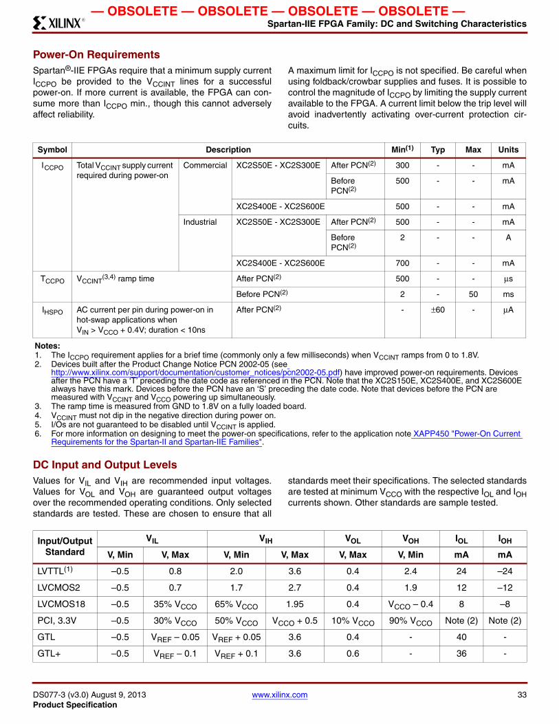
Spartan-IIE FPGA Family: DC and Switching CharacteristicsR
— OBSOLETE — OBSOLETE — OBSOLETE — OBSOLETE —
Power-On RequirementsSpartan®-IIE FPGAs require that a minimum supply current ICCPO be provided to the VCCINT lines for a successful power-on. If more current is available, the FPGA can con-sume more than ICCPO min., though this cannot adversely affect reliability.
A maximum limit for ICCPO is not specified. Be careful when using foldback/crowbar supplies and fuses. It is possible to control the magnitude of ICCPO by limiting the supply current available to the FPGA. A current limit below the trip level will avoid inadvertently activating over-current protection cir-cuits.
DC Input and Output LevelsValues for VIL and VIH are recommended input voltages. Values for VOL and VOH are guaranteed output voltages over the recommended operating conditions. Only selected standards are tested. These are chosen to ensure that all
standards meet their specifications. The selected standards are tested at minimum VCCO with the respective IOL and IOHcurrents shown. Other standards are sample tested.
Symbol Description Min(1) Typ Max Units
I CCPO Total VCCINT supply current required during power-on
Commercial XC2S50E - XC2S300E After PCN(2) 300 - - mA
Before PCN(2)
500 - - mA
XC2S400E - XC2S600E 500 - - mA
Industrial XC2S50E - XC2S300E After PCN(2) 500 - - mA
Before PCN(2)
2 - - A
XC2S400E - XC2S600E 700 - - mA
TCCPO VCCINT(3,4) ramp time After PCN(2) 500 - - μs
Before PCN(2) 2 - 50 ms
IHSPO AC current per pin during power-on in hot-swap applications when VIN > VCCO + 0.4V; duration < 10ns
After PCN(2) - ±60 - μA
Notes: 1. The ICCPO requirement applies for a brief time (commonly only a few milliseconds) when VCCINT ramps from 0 to 1.8V.2. Devices built after the Product Change Notice PCN 2002-05 (see
http://www.xilinx.com/support/documentation/customer_notices/pcn2002-05.pdf) have improved power-on requirements. Devices after the PCN have a ‘T’ preceding the date code as referenced in the PCN. Note that the XC2S150E, XC2S400E, and XC2S600E always have this mark. Devices before the PCN have an ‘S’ preceding the date code. Note that devices before the PCN are measured with VCCINT and VCCO powering up simultaneously.
3. The ramp time is measured from GND to 1.8V on a fully loaded board.4. VCCINT must not dip in the negative direction during power on.5. I/Os are not guaranteed to be disabled until VCCINT is applied.6. For more information on designing to meet the power-on specifications, refer to the application note XAPP450 "Power-On Current
Requirements for the Spartan-II and Spartan-IIE Families".
Input/OutputStandard
VIL VIH VOL VOH IOL IOH
V, Min V, Max V, Min V, Max V, Max V, Min mA mA
LVTTL(1) –0.5 0.8 2.0 3.6 0.4 2.4 24 –24
LVCMOS2 –0.5 0.7 1.7 2.7 0.4 1.9 12 –12
LVCMOS18 –0.5 35% VCCO 65% VCCO 1.95 0.4 VCCO – 0.4 8 –8
PCI, 3.3V –0.5 30% VCCO 50% VCCO VCCO + 0.5 10% VCCO 90% VCCO Note (2) Note (2)
GTL –0.5 VREF – 0.05 VREF + 0.05 3.6 0.4 - 40 -
GTL+ –0.5 VREF – 0.1 VREF + 0.1 3.6 0.6 - 36 -
DS077-3 (v3.0) August 9, 2013 www.xilinx.com 33Product Specification

Spartan-IIE FPGA Family: DC and Switching CharacteristicsR
— OBSOLETE — OBSOLETE — OBSOLETE — OBSOLETE —
LVDS DC Specifications
LVPECL DC SpecificationsThese values are valid at the output of the source termina-tion pack shown under LVPECL, with a 100Ω differential load only. The VOH levels are 200 mV below standard
LVPECL levels and are compatible with devices tolerant of lower common-mode ranges. The following table summa-rizes the DC output specifications of LVPECL.
HSTL I –0.5 VREF – 0.1 VREF + 0.1 3.6 0.4 VCCO – 0.4 8 –8
HSTL III –0.5 VREF – 0.1 VREF + 0.1 3.6 0.4 VCCO – 0.4 24 –8
HSTL IV –0.5 VREF – 0.1 VREF + 0.1 3.6 0.4 VCCO – 0.4 48 –8
SSTL3 I –0.5 VREF – 0.2 VREF + 0.2 3.6 VREF – 0.6 VREF + 0.6 8 –8
SSTL3 II –0.5 VREF – 0.2 VREF + 0.2 3.6 VREF – 0.8 VREF + 0.8 16 –16
SSTL2 I –0.5 VREF – 0.2 VREF + 0.2 3.6 VREF – 0.61 VREF + 0.61 7.6 –7.6
SSTL2 II –0.5 VREF – 0.2 VREF + 0.2 3.6 VREF – 0.8 VREF + 0.8 15.2 –15.2
CTT –0.5 VREF – 0.2 VREF + 0.2 3.6 VREF – 0.4 VREF + 0.4 8 –8
AGP –0.5 VREF – 0.2 VREF + 0.2 3.6 10% VCCO 90% VCCO Note (2) Note (2)
Notes: 1. VOL and VOH for lower drive currents are sample tested.2. Tested according to the relevant specifications.
Symbol Description Conditions Min Typ Max Units
VCCO Supply voltage 2.375 2.5 2.625 V
VOH Output High voltage for Q and Q RT = 100Ω across Q and Q signals 1.25 1.425 1.6 V
VOL Output Low voltage for Q and Q RT = 100Ω across Q and Q signals 0.9 1.075 1.25 V
VODIFF Differential output voltage (Q – Q), Q = High or (Q – Q), Q = High
RT = 100Ω across Q and Q signals 250 350 450 mV
VOCM Output common-mode voltage RT = 100Ω across Q and Q signals 1.125 1.25 1.375 V
VIDIFF Differential input voltage (Q – Q), Q = High or (Q – Q), Q = High
Common-mode input voltage = 1.25 V 100 350 - mV
VICM Input common-mode voltage Differential input voltage = ±350 mV 0.2 1.25 2.2 V
Input/OutputStandard
VIL VIH VOL VOH IOL IOH
V, Min V, Max V, Min V, Max V, Max V, Min mA mA
DC Parameter Min Max Min Max Min Max Units
VCCO 3.0 3.3 3.6 V
VOH 1.8 2.11 1.92 2.28 2.13 2.41 V
VOL 0.96 1.27 1.06 1.43 1.30 1.57 V
VIH 1.49 2.72 1.49 2.72 1.49 2.72 V
VIL 0.86 2.125 0.86 2.125 0.86 2.125 V
Differential input voltage 0.3 - 0.3 - 0.3 - V
34 www.xilinx.com DS077-3 (v3.0) August 9, 2013Product Specification
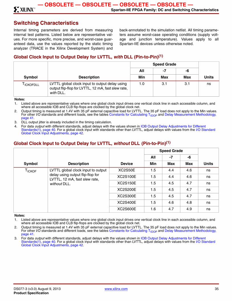
Spartan-IIE FPGA Family: DC and Switching CharacteristicsR
— OBSOLETE — OBSOLETE — OBSOLETE — OBSOLETE —
Switching CharacteristicsInternal timing parameters are derived from measuring internal test patterns. Listed below are representative val-ues. For more specific, more precise, and worst-case guar-anteed data, use the values reported by the static timing analyzer (TRACE in the Xilinx Development System) and
back-annotated to the simulation netlist. All timing parame-ters assume worst-case operating conditions (supply volt-age and junction temperature). Values apply to all Spartan-IIE devices unless otherwise noted.
Global Clock Input to Output Delay for LVTTL, with DLL (Pin-to-Pin)(1)
Global Clock Input to Output Delay for LVTTL, without DLL (Pin-to-Pin)(1)
Symbol Description
Speed Grade
Units
All -7 -6
Min Max Max
TICKOFDLL LVTTL global clock input to output delay using output flip-flop for LVTTL, 12 mA, fast slew rate, with DLL.
1.0 3.1 3.1 ns
Notes: 1. Listed above are representative values where one global clock input drives one vertical clock line in each accessible column, and
where all accessible IOB and CLB flip-flops are clocked by the global clock net.2. Output timing is measured at 1.4V with 35 pF external capacitive load for LVTTL. The 35 pF load does not apply to the Min values.
For other I/O standards and different loads, see the tables Constants for Calculating TIOOP and Delay Measurement Methodology, page 41.
3. DLL output jitter is already included in the timing calculation.4. For data output with different standards, adjust delays with the values shown in IOB Output Delay Adjustments for Different
Standards(1), page 40. For a global clock input with standards other than LVTTL, adjust delays with values from the I/O Standard Global Clock Input Adjustments, page 42.
Symbol Description Device
Speed Grade
Units
All -7 -6
Min Max Max
TICKOF LVTTL global clock input to output delay using output flip-flop for LVTTL, 12 mA, fast slew rate, without DLL.
XC2S50E 1.5 4.4 4.6 ns
XC2S100E 1.5 4.4 4.6 ns
XC2S150E 1.5 4.5 4.7 ns
XC2S200E 1.5 4.5 4.7 ns
XC2S300E 1.5 4.5 4.7 ns
XC2S400E 1.5 4.6 4.8 ns
XC2S600E 1.6 4.7 4.9 ns
Notes: 1. Listed above are representative values where one global clock input drives one vertical clock line in each accessible column, and
where all accessible IOB and CLB flip-flops are clocked by the global clock net.2. Output timing is measured at 1.4V with 35 pF external capacitive load for LVTTL. The 35 pF load does not apply to the Min values.
For other I/O standards and different loads, see the tables Constants for Calculating TIOOP and Delay Measurement Methodology, page 41.
3. For data output with different standards, adjust delays with the values shown in IOB Output Delay Adjustments for Different Standards(1), page 40. For a global clock input with standards other than LVTTL, adjust delays with values from the I/O Standard Global Clock Input Adjustments, page 42.
DS077-3 (v3.0) August 9, 2013 www.xilinx.com 35Product Specification

Spartan-IIE FPGA Family: DC and Switching CharacteristicsR
— OBSOLETE — OBSOLETE — OBSOLETE — OBSOLETE —
Global Clock Setup and Hold for LVTTL Standard, with DLL (Pin-to-Pin)
Global Clock Setup and Hold for LVTTL Standard, without DLL (Pin-to-Pin)
Symbol Description
Speed Grade
Units
-7 -6
Min Min
TPSDLL / TPHDLL Input setup and hold time relative to global clock input signal for LVTTL standard, no delay, IFF,(1) with DLL
1.6 / 0 1.7 / 0 ns
Notes: 1. IFF = Input Flip-Flop or Latch2. Setup time is measured relative to the Global Clock input signal with the fastest route and the lightest load. Hold time is measured
relative to the Global Clock input signal with the slowest route and heaviest load.3. DLL output jitter is already included in the timing calculation.4. For data input with different standards, adjust the setup time delay by the values shown in IOB Input Delay Adjustments for Different
Standards, page 38. For a global clock input with standards other than LVTTL, adjust delays with values from the I/O Standard Global Clock Input Adjustments, page 42.
5. A zero hold time listing indicates no hold time or a negative hold time.
Symbol Description Device
Speed Grade
Units
-7 -6
Min Min
TPSFD / TPHFD Input setup and hold time relative to global clock input signal for LVTTL standard, with delay, IFF,(1) without DLL
XC2S50E 1.8 / 0 1.8 / 0 ns
XC2S100E 1.8 / 0 1.8 / 0 ns
XC2S150E 1.9 / 0 1.9 / 0 ns
XC2S200E 1.9 / 0 1.9 / 0 ns
XC2S300E 2.0 / 0 2.0 / 0 ns
XC2S400E 2.0 / 0 2.0 / 0 ns
XC2S600E 2.1 / 0 2.1 / 0 ns
Notes: 1. IFF = Input Flip-Flop or Latch2. Setup time is measured relative to the Global Clock input signal with the fastest route and the lightest load. Hold time is measured
relative to the Global Clock input signal with the slowest route and heaviest load.3. For data input with different standards, adjust the setup time delay by the values shown in IOB Input Delay Adjustments for Different
Standards, page 38. For a global clock input with standards other than LVTTL, adjust delays with values from the I/O Standard Global Clock Input Adjustments, page 42.
36 www.xilinx.com DS077-3 (v3.0) August 9, 2013Product Specification

Spartan-IIE FPGA Family: DC and Switching CharacteristicsR
— OBSOLETE — OBSOLETE — OBSOLETE — OBSOLETE —
IOB Input Switching Characteristics (1)
Input delays associated with the pad are specified for LVTTL levels. For other standards, adjust the delays with the values shown in IOB Input Delay Adjustments for Different Standards, page 38.
Symbol Description Device
Speed Grade
Units
-7 -6
Min Max Min Max
Propagation Delays
TIOPI Pad to I output, no delay All 0.4 0.8 0.4 0.8 ns
TIOPID Pad to I output, with delay All 0.5 1.0 0.5 1.0 ns
TIOPLI Pad to output IQ via transparent latch, no delay
All 0.7 1.5 0.7 1.6 ns
TIOPLID Pad to output IQ via transparent latch, with delay
XC2S50E 1.3 3.0 1.3 3.1 ns
XC2S100E 1.3 3.0 1.3 3.1 ns
XC2S150E 1.3 3.2 1.3 3.3 ns
XC2S200E 1.3 3.2 1.3 3.3 ns
XC2S300E 1.3 3.2 1.3 3.3 ns
XC2S400E 1.4 3.2 1.4 3.4 ns
XC2S600E 1.5 3.5 1.5 3.7 ns
Sequential Delays
TIOCKIQ Clock CLK to output IQ All 0.1 0.7 0.1 0.7 ns
Setup/Hold Times with Respect to Clock CLK
TIOPICK / TIOICKP Pad, no delay All 1.4 / 0 - 1.5 / 0 - ns
TIOPICKD / TIOICKPD Pad, with delay XC2S50E 2.9 / 0 - 2.9 / 0 - ns
XC2S100E 2.9 / 0 - 2.9 / 0 - ns
XC2S150E 3.1 / 0 - 3.1 / 0 - ns
XC2S200E 3.1 / 0 - 3.1 / 0 - ns
XC2S300E 3.1 / 0 - 3.1 / 0 - ns
XC2S400E 3.2 / 0 - 3.2 / 0 - ns
XC2S600E 3.5 / 0 - 3.5 / 0 - ns
TIOICECK / TIOCKICE ICE input All 0.7 / 0.01 - 0.7 / 0.01 - ns
Set/Reset Delays
TIOSRCKI SR input (IFF, synchronous) All 0.9 - 1.0 - ns
TIOSRIQ SR input to IQ (asynchronous) All 0.5 1.2 0.5 1.4 ns
TGSRQ GSR to output IQ All 3.8 8.5 3.8 9.7 ns
Notes: 1. Input timing for LVTTL is measured at 1.4V. For other I/O standards, see the table Delay Measurement Methodology, page 41.
DS077-3 (v3.0) August 9, 2013 www.xilinx.com 37Product Specification
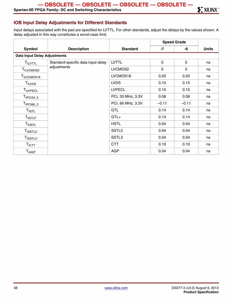
Spartan-IIE FPGA Family: DC and Switching CharacteristicsR
— OBSOLETE — OBSOLETE — OBSOLETE — OBSOLETE —
IOB Input Delay Adjustments for Different Standards
Input delays associated with the pad are specified for LVTTL. For other standards, adjust the delays by the values shown. A delay adjusted in this way constitutes a worst-case limit.
Symbol Description Standard
Speed Grade
Units-7 -6
Data Input Delay Adjustments
TILVTTL Standard-specific data input delay adjustments
LVTTL 0 0 ns
TILVCMOS2 LVCMOS2 0 0 ns
TILVCMOS18 LVCMOS18 0.20 0.20 ns
TILVDS LVDS 0.15 0.15 ns
TILVPECL LVPECL 0.15 0.15 ns
TIPCI33_3 PCI, 33 MHz, 3.3V 0.08 0.08 ns
TIPCI66_3 PCI, 66 MHz, 3.3V –0.11 –0.11 ns
TIGTL GTL 0.14 0.14 ns
TIGTLP GTL+ 0.14 0.14 ns
TIHSTL HSTL 0.04 0.04 ns
TISSTL2 SSTL2 0.04 0.04 ns
TISSTL3 SSTL3 0.04 0.04 ns
TICTT CTT 0.10 0.10 ns
TIAGP AGP 0.04 0.04 ns
38 www.xilinx.com DS077-3 (v3.0) August 9, 2013Product Specification

Spartan-IIE FPGA Family: DC and Switching CharacteristicsR
— OBSOLETE — OBSOLETE — OBSOLETE — OBSOLETE —
IOB Output Switching Characteristics
Output delays terminating at a pad are specified for LVTTL with 12 mA drive and fast slew rate. For other standards, adjust the delays with the values shown in IOB Output Delay Adjustments for Different Standards(1), page 40.
Symbol Description
Speed Grade
Units
-7 -6
Min Max Min Max
Propagation Delays
TIOOP O input to pad 1.0 2.7 1.0 2.9 ns
TIOOLP O input to pad via transparent latch 1.2 3.1 1.2 3.4 ns
3-state Delays
TIOTHZ T input to pad high impedance (1) 0.7 1.7 0.7 1.9 ns
TIOTON T input to valid data on pad 1.1 2.9 1.1 3.1 ns
TIOTLPHZ T input to pad high impedance via transparent latch (1) 0.8 2.0 0.8 2.2 ns
TIOTLPON T input to valid data on pad via transparent latch 1.2 3.2 1.2 3.4 ns
TGTS GTS to pad high impedance (1) 1.9 4.6 1.9 4.9 ns
Sequential Delays
TIOCKP Clock CLK to pad 0.9 2.8 0.9 2.9 ns
TIOCKHZ Clock CLK to pad high impedance (synchronous)(1) 0.7 2.0 0.7 2.2 ns
TIOCKON Clock CLK to valid data on pad (synchronous) 1.1 3.2 1.1 3.4 ns
Setup/Hold Times with Respect to Clock CLK
TIOOCK / TIOCKO O input 1.0 / 0 - 1.1 / 0 - ns
TIOOCECK / TIOCKOCE OCE input 0.7 / 0 - 0.7 / 0 - ns
TIOSRCKO / TIOCKOSR SR input (OFF) 0.9 / 0 - 1.0 / 0 - ns
TIOTCK / TIOCKT 3-state setup times, T input 0.6 / 0 - 0.7 / 0 - ns
TIOTCECK / TIOCKTCE 3-state setup times, TCE input 0.6 / 0 - 0.8 / 0 - ns
TIOSRCKT / TIOCKTSR 3-state setup times, SR input (TFF) 0.9 / 0 - 1.0 / 0 - ns
Set/Reset Delays
TIOSRP SR input to pad (asynchronous) 1.2 3.3 1.2 3.5 ns
TIOSRHZ SR input to pad high impedance (asynchronous)(1) 1.0 2.4 1.0 2.7 ns
TIOSRON SR input to valid data on pad (asynchronous) 1.4 3.7 1.4 3.9 ns
TIOGSRQ GSR to pad 3.8 8.5 3.8 9.7 ns
Notes: 1. Three-state turn-off delays should not be adjusted.
DS077-3 (v3.0) August 9, 2013 www.xilinx.com 39Product Specification

Spartan-IIE FPGA Family: DC and Switching CharacteristicsR
— OBSOLETE — OBSOLETE — OBSOLETE — OBSOLETE —
IOB Output Delay Adjustments for Different Standards(1)
Output delays terminating at a pad are specified for LVTTL with 12 mA drive and fast slew rate. For other standards, adjust the delays by the values shown. A delay adjusted in this way constitutes a worst-case limit.
Symbol Description Standard
Speed Grade
Units-7 -6
Output Delay Adjustments (Adj)
TOLVTTL_S2 Standard-specific adjustments for output delays terminating at pads (based on standard capacitive load, CSL)
LVTTL, Slow, 2 mA 14.7 14.7 ns
TOLVTTL_S4 4 mA 7.5 7.5 ns
TOLVTTL_S6 6 mA 4.8 4.8 ns
TOLVTTL_S8 8 mA 3.0 3.0 ns
TOLVTTL_S12 12 mA 1.9 1.9 ns
TOLVTTL_S16 16 mA 1.7 1.7 ns
TOLVTTL_S24 24 mA 1.3 1.3 ns
TOLVTTL_F2 LVTTL, Fast, 2 mA 13.1 13.1 ns
TOLVTTL_F4 4 mA 5.3 5.3 ns
TOLVTTL_F6 6 mA 3.1 3.1 ns
TOLVTTL_F8 8 mA 1.0 1.0 ns
TOLVTTL_F12 12 mA 0 0 ns
TOLVTTL_F16 16 mA –0.05 –0.05 ns
TOLVTTL_F24 24 mA –0.20 –0.20 ns
TOLVCMOS2 LVCMOS2 0.09 0.09 ns
TOLVCMOS18 LVCMOS18 0.7 0.7 ns
TOLVDS LVDS –1.2 –1.2 ns
TOLVPECL LVPECL –0.41 –0.41 ns
TOPCI33_3 PCI, 33 MHz, 3.3V 2.3 2.3 ns
TOPCI66_3 PCI, 66 MHz, 3.3V –0.41 –0.41 ns
TOGTL GTL 0.49 0.49 ns
TOGTLP GTL+ 0.8 0.8 ns
TOHSTL_I HSTL I –0.51 –0.51 ns
TOHSTL_III HSTL III –0.91 –0.91 ns
TOHSTL_IV HSTL IV –1.01 –1.01 ns
TOSSTL2_I SSTL2 I –0.51 –0.51 ns
TOSSLT2_II SSTL2 II –0.91 –0.91 ns
TOSSTL3_I SSTL3 I –0.51 –0.51 ns
TOSSTL3_II SSTL3 II –1.01 –1.01 ns
TOCTT CTT –0.61 –0.61 ns
TOAGP AGP –0.91 –0.91 ns
Notes: 1. Output timing is measured at 1.4V with 35 pF external capacitive load for LVTTL. For other I/O standards and different loads, see the
tables Constants for Calculating TIOOP and Delay Measurement Methodology, page 41.
40 www.xilinx.com DS077-3 (v3.0) August 9, 2013Product Specification

Spartan-IIE FPGA Family: DC and Switching CharacteristicsR
— OBSOLETE — OBSOLETE — OBSOLETE — OBSOLETE —
Calculation of TIOOP as a Function of CapacitanceTIOOP is the propagation delay from the O Input of the IOB to the pad. The values for TIOOP are based on the standard capacitive load (CSL) for each I/O standard as listed in the table Constants for Calculating TIOOP, below.
For other capacitive loads, use the formulas below to calcu-late an adjusted propagation delay, TIOOP1.
TIOOP1 = TIOOP + Adj + (CLOAD – CSL) * FL
Where:
Adj is selected from IOB Output Delay Adjustments for Different Standards(1), page 40, according to the I/O standard used
CLOAD is the capacitive load for the design
FL is the capacitance scaling factor
Delay Measurement Methodology
Standard VL(1) VH
(1)Meas. Point
VREF Typ (2)
LVTTL 0 3 1.4 -
LVCMOS2 0 2.5 1.125 -
PCI33_3 Per PCI Spec -
PCI66_3 Per PCI Spec -
GTL VREF – 0.2 VREF + 0.2 VREF 0.80
GTL+ VREF – 0.2 VREF + 0.2 VREF 1.0
HSTL Class I VREF – 0.5 VREF + 0.5 VREF 0.75
HSTL Class III VREF – 0.5 VREF + 0.5 VREF 0.90
HSTL Class IV VREF – 0.5 VREF + 0.5 VREF 0.90
SSTL3 I and II VREF – 1.0 VREF + 1.0 VREF 1.5
SSTL2 I and II VREF – 0.75 VREF + 0.75 VREF 1.25
CTT VREF – 0.2 VREF + 0.2 VREF 1.5
AGP VREF – (0.2xVCCO)
VREF + (0.2xVCCO)
VREF Per AGP Spec
LVDS 1.2 – 0.125 1.2 + 0.125 1.2
LVPECL 1.6 – 0.3 1.6 + 0.3 1.6
Notes: 1. Input waveform switches between VL and VH.2. Measurements are made at VREF Typ, Maximum, and
Minimum. Worst-case values are reported. 3. I/O parameter measurements are made with the capacitance
values shown in the following table, Constants for Calculating TIOOP. Refer to Application Note XAPP179 for appropriate terminations.
4. I/O standard measurements are reflected in the IBIS model information except where the IBIS format precludes it.
Constants for Calculating TIOOP
StandardCSL
(1) (pF)
FL (ns/pF)
LVTTL Fast Slew Rate, 2 mA drive 35 0.41
LVTTL Fast Slew Rate, 4 mA drive 35 0.20
LVTTL Fast Slew Rate, 6 mA drive 35 0.13
LVTTL Fast Slew Rate, 8 mA drive 35 0.079
LVTTL Fast Slew Rate, 12 mA drive 35 0.044
LVTTL Fast Slew Rate, 16 mA drive 35 0.043
LVTTL Fast Slew Rate, 24 mA drive 35 0.033
LVTTL Slow Slew Rate, 2 mA drive 35 0.41
LVTTL Slow Slew Rate, 4 mA drive 35 0.20
LVTTL Slow Slew Rate, 6 mA drive 35 0.100
LVTTL Slow Slew Rate, 8 mA drive 35 0.086
LVTTL Slow Slew Rate, 12 mA drive 35 0.058
LVTTL Slow Slew Rate, 16 mA drive 35 0.050
LVTTL Slow Slew Rate, 24 mA drive 35 0.048
LVCMOS2 35 0.041
LVCMOS18 35 0.050
PCI 33 MHz 3.3V 10 0.050
PCI 66 MHz 3.3V 10 0.033
GTL 0 0.014
GTL+ 0 0.017
HSTL Class I 20 0.022
HSTL Class III 20 0.016
HSTL Class IV 20 0.014
SSTL2 Class I 30 0.028
SSTL2 Class II 30 0.016
SSTL3 Class I 30 0.029
SSTL3 Class II 30 0.016
CTT 20 0.035
AGP 10 0.037
Notes: 1. I/O parameter measurements are made with the capacitance
values shown above. Refer to Application Note XAPP179 for appropriate terminations.
2. I/O standard measurements are reflected in the IBIS model information except where the IBIS format precludes it.
DS077-3 (v3.0) August 9, 2013 www.xilinx.com 41Product Specification
Spartan-IIE FPGA Family: DC and Switching CharacteristicsR
— OBSOLETE — OBSOLETE — OBSOLETE — OBSOLETE —
Clock Distribution Switching Characteristics
TGPIO is specified for LVTTL levels. For other standards, adjust TGPIO with the values shown in I/O Standard Global Clock Input Adjustments.
I/O Standard Global Clock Input Adjustments
Delays associated with a global clock input pad are specified for LVTTL levels. For other standards, adjust the delays by the values shown. A delay adjusted in this way constitutes a worst-case limit.
Symbol Description
Speed Grade
Units
-7 -6
Max Max
GCLK IOB and Buffer
TGPIO Global clock pad to output 0.7 0.7 ns
TGIO Global clock buffer I input to O output 0.45 0.5 ns
Symbol Description Standard
Speed Grade
Units-7 -6
Data Input Delay Adjustments
TGPLVTTL Standard-specific global clock input delay adjustments
LVTTL 0 0 ns
TGPLVCMOS2 LVCMOS2 0 0 ns
TGPLVCMOS18 LVCMOS18 0.2 0.2 ns
TGPLVCDS LVDS 0.38 0.38 ns
TGPLVPECL LVCPECL 0.38 0.38 ns
TGPPCI33_3 PCI, 33 MHz, 3.3V 0.08 0.08 ns
TGPPCI66_3 PCI, 66 MHz, 3.3V –0.11 –0.11 ns
TGPGTL GTL 0.37 0.37 ns
TGPGTLP GTL+ 0.37 0.37 ns
TGPHSTL HSTL 0.27 0.27 ns
TGPSSTL2 SSTL2 0.27 0.27 ns
TGPSSTL3 SSTL3 0.27 0.27 ns
TGPCTT CTT 0.33 0.33 ns
TGPAGP AGP 0.27 0.27 ns
Notes: 1. Input timing for GPLVTTL is measured at 1.4V. For other I/O standards, see the table Delay Measurement Methodology, page 41.
42 www.xilinx.com DS077-3 (v3.0) August 9, 2013Product Specification

Spartan-IIE FPGA Family: DC and Switching CharacteristicsR
— OBSOLETE — OBSOLETE — OBSOLETE — OBSOLETE —
DLL Timing ParametersBecause of the difficulty in directly measuring many internal timing parameters, those parameters are derived from benchmark timing patterns. The following guidelines reflect
worst-case values across the recommended operating con-ditions.
DLL Clock Tolerance, Jitter, and Phase Information All DLL output jitter and phase specifications were deter-mined through statistical measurement at the package pins using a clock mirror configuration and matched drivers.
Figure 22, page 44, provides definitions for various parame-ters in the table below.
Symbol Description FCLKIN
Speed Grade
Units
-7 -6
Min Max Min Max
FCLKINHF Input clock frequency (CLKDLLHF) - 60 320 60 275 MHz
FCLKINLF Input clock frequency (CLKDLL) - 25 160 25 135 MHz
TDLLPW Input clock pulse width ≥25 MHz 5.0 - 5.0 - ns
≥50 MHz 3.0 - 3.0 - ns
≥100 MHz 2.4 - 2.4 - ns
≥150 MHz 2.0 - 2.0 - ns
≥200 MHz 1.8 - 1.8 - ns
≥250 MHz 1.5 - 1.5 - ns
≥300 MHz 1.3 - NA -
Symbol Description FCLKIN
CLKDLLHF CLKDLL
UnitsMin Max Min Max
TIPTOL Input clock period tolerance - 1.0 - 1.0 ns
TIJITCC Input clock jitter tolerance (cycle-to-cycle) - ±150 - ± 300 ps
TLOCK Time required for DLL to acquire lock(1) > 60 MHz - 20 - 20 μs
50-60 MHz - - - 25 μs
40-50 MHz - - - 50 μs
30-40 MHz - - - 90 μs
25-30 MHz - - - 120 μs
TOJITCC Output jitter (cycle-to-cycle) for any DLL clock output (2) - ± 60 - ± 60 ps
TPHIO Phase offset between CLKIN and CLKO (3) - ±100 - ±100 ps
TPHOO Phase offset between clock outputs on the DLL(4) - ±140 - ±140 ps
TPHIOM Phase difference between CLKIN and CLKO (5) - ±160 - ±160 ps
TPHOOM Phase difference between clock outputs on the DLL(6) - ± 200 - ± 200 ps
Notes: 1. Commercial operating conditions. Add 30% for Industrial operating conditions.2. Output Jitter is cycle-to-cycle jitter measured on the DLL output clock, excluding input clock jitter.3. Phase Offset between CLKIN and CLKO is the worst-case fixed time difference between rising edges of CLKIN and CLKO,
excluding output jitter and input clock jitter.4. Phase Offset between Clock Outputs on the DLL is the worst-case fixed time difference between rising edges of any two DLL
outputs, excluding output jitter and input clock jitter.5. Maximum Phase Difference between CLKIN and CLKO is the sum of output jitter and phase offset between CLKIN and CLKO, or
the greatest difference between CLKIN and CLKO rising edges due to DLL alone (excluding input clock jitter).6. Maximum Phase Difference between Clock Outputs on the DLL is the sum of output jitter and phase offset between any DLL
clock outputs, or the greatest difference between any two DLL output rising edges due to DLL alone (excluding input clock jitter).
DS077-3 (v3.0) August 9, 2013 www.xilinx.com 43Product Specification
Spartan-IIE FPGA Family: DC and Switching CharacteristicsR
— OBSOLETE — OBSOLETE — OBSOLETE — OBSOLETE —
Figure 22: Period Tolerance and Clock Jitter
Period Tolerance: the allowed input clock period change in nanoseconds.
Output Jitter: the difference between an idealreference clock edge and the actual design.
TCLKIN + TIPTOL_
DS001_52_090800
Actual Period
+ J
itter
+/- Jitter
+ Maximum Phase Difference
Phase Offset and Maximum Phase Difference
+ Phase Offset
Ideal Period
1
FCLKIN T = CLKIN
44 www.xilinx.com DS077-3 (v3.0) August 9, 2013Product Specification

Spartan-IIE FPGA Family: DC and Switching CharacteristicsR
— OBSOLETE — OBSOLETE — OBSOLETE — OBSOLETE —
CLB Switching Characteristics
Delays originating at F/G inputs vary slightly according to the input used. The values listed below are worst-case. Precise values are provided by the timing analyzer.
Symbol Description
Speed Grade
Units
-7 -6
Min Max Min Max
Combinatorial Delays
TILO 4-input function: F/G inputs to X/Y outputs 0.18 0.42 0.18 0.47 ns
TIF5 5-input function: F/G inputs to F5 output 0.3 0.8 0.3 0.9 ns
TIF5X 5-input function: F/G inputs to X output 0.3 0.8 0.3 0.9 ns
TIF6Y 6-input function: F/G inputs to Y output via F6 MUX 0.3 0.9 0.3 1.0 ns
TF5INY 6-input function: F5IN input to Y output 0.04 0.2 0.04 0.22 ns
TIFNCTL Incremental delay routing through transparent latch to XQ/YQ outputs
- 0.7 - 0.8 ns
TBYYB BY input to YB output 0.18 0.46 0.18 0.51 ns
Sequential Delays
TCKO FF clock CLK to XQ/YQ outputs 0.3 0.9 0.3 1.0 ns
TCKLO Latch clock CLK to XQ/YQ outputs 0.3 0.9 0.3 1.0 ns
Setup/Hold Times with Respect to Clock CLK
TICK / TCKI 4-input function: F/G inputs 1.0 / 0 - 1.1 / 0 - ns
TIF5CK / TCKIF5 5-input function: F/G inputs 1.4 / 0 - 1.5 / 0 - ns
TF5INCK / TCKF5IN 6-input function: F5IN input 0.8 / 0 - 0.8 / 0 - ns
TIF6CK / TCKIF6 6-input function: F/G inputs via F6 MUX 1.5 / 0 - 1.6 / 0 - ns
TDICK / TCKDI BX/BY inputs 0.7 / 0 - 0.8 / 0 - ns
TCECK / TCKCE CE input 0.7 / 0 - 0.7 / 0 - ns
TRCK / TCKR SR/BY inputs (synchronous) 0.52 / 0 - 0.6 / 0 - ns
Clock CLK
TCH Pulse width, High 1.3 - 1.4 - ns
TCL Pulse width, Low 1.3 - 1.4 - ns
Set/Reset
TRPW Pulse width, SR/BY inputs 2.1 - 2.4 - ns
TRQ Delay from SR/BY inputs to XQ/YQ outputs (asynchronous)
0.3 0.9 0.3 1.0 ns
FTOG Toggle frequency (for export control) - 400 - 357 MHz
DS077-3 (v3.0) August 9, 2013 www.xilinx.com 45Product Specification

Spartan-IIE FPGA Family: DC and Switching CharacteristicsR
— OBSOLETE — OBSOLETE — OBSOLETE — OBSOLETE —
CLB Arithmetic Switching Characteristics
Setup times not listed explicitly can be approximated by decreasing the combinatorial delays by the setup time adjustment listed. Precise values are provided by the timing analyzer.
Symbol Description
Speed Grade
Units
-7 -6
Min Max Min Max
Combinatorial Delays
TOPX F operand inputs to X via XOR - 0.8 - 0.8 ns
TOPXB F operand input to XB output - 0.8 - 0.9 ns
TOPY F operand input to Y via XOR - 1.4 - 1.5 ns
TOPYB F operand input to YB output - 1.1 - 1.3 ns
TOPCYF F operand input to COUT output - 0.9 - 1.0 ns
TOPGY G operand inputs to Y via XOR - 0.8 - 0.9 ns
TOPGYB G operand input to YB output - 1.2 - 1.3 ns
TOPCYG G operand input to COUT output - 0.9 - 1.0 ns
TBXCY BX initialization input to COUT - 0.51 - 0.6 ns
TCINX CIN input to X output via XOR - 0.6 - 0.7 ns
TCINXB CIN input to XB - 0.07 - 0.1 ns
TCINY CIN input to Y via XOR - 0.7 - 0.7 ns
TCINYB CIN input to YB - 0.4 - 0.5 ns
TBYP CIN input to COUT output - 0.14 - 0.15 ns
Multiplier Operation
TFANDXB F1/2 operand inputs to XB output via AND - 0.35 - 0.4 ns
TFANDYB F1/2 operand inputs to YB output via AND - 0.7 - 0.8 ns
TFANDCY F1/2 operand inputs to COUT output via AND - 0.5 - 0.6 ns
TGANDYB G1/2 operand inputs to YB output via AND - 0.6 - 0.7 ns
TGANDCY G1/2 operand inputs to COUT output via AND - 0.3 - 0.4 ns
Setup/Hold Times with Respect to Clock CLK
TCCKX / TCKCX CIN input to FFX 1.2 / 0 - 1.3 / 0 - ns
TCCKY / TCKCY CIN input to FFY 1.2 / 0 - 1.3 / 0 - ns
46 www.xilinx.com DS077-3 (v3.0) August 9, 2013Product Specification

Spartan-IIE FPGA Family: DC and Switching CharacteristicsR
— OBSOLETE — OBSOLETE — OBSOLETE — OBSOLETE —
CLB Distributed RAM Switching Characteristics
CLB Shift Register Switching Characteristics
Block RAM Switching Characteristics
Symbol Description
Speed Grade
Units
-7 -6
Min Max Min MaxSequential Delays
TSHCKO16 Clock CLK to X/Y outputs (WE active, 16 x 1 mode) 0.6 1.5 0.6 1.7 ns
TSHCKO32 Clock CLK to X/Y outputs (WE active, 32 x 1 mode) 0.8 1.9 0.8 2.1 ns
Setup/Hold Times with Respect to Clock CLK
TAS / TAH F/G address inputs 0.42 / 0 - 0.5 / 0 - ns
TDS / TDH BX/BY data inputs (DIN) 0.53 / 0 - 0.6 / 0 - ns
TWS / TWH CE input (WS) 0.7 / 0 - 0.8 / 0 - ns
Clock CLK
TWPH Pulse width, High 2.1 - 2.4 - ns
TWPL Pulse width, Low 2.1 - 2.4 - ns
TWC Clock period to meet address write cycle time 4.2 - 4.8 - ns
Symbol Description
Speed Grade
Units
-7 -6
Min Max Min MaxSequential Delays
TREG Clock CLK to X/Y outputs 1.2 2.9 1.2 3.2 ns
Setup/Hold Times with Respect to Clock CLK
TSHDICK BX/BY data inputs (DIN) 0.53 / 0 - 0.6 / 0 - ns
TSHCECK CE input (WS) 0.7 / 0 - 0.8 / 0 - ns
Clock CLK
TSRPH Pulse width, High 2.1 - 2.4 - ns
TSRPL Pulse width, Low 2.1 - 2.4 - ns
Symbol Description
Speed Grade
Units
-7 -6
Min Max Min MaxSequential Delays
TBCKO Clock CLK to DOUT output 0.6 3.1 0.6 3.5 ns
Setup/Hold Times with Respect to Clock CLK
TBACK / TBCKA ADDR inputs 1.0 / 0 - 1.1 / 0 - ns
TBDCK/ TBCKD DIN inputs 1.0 / 0 - 1.1 / 0 - ns
TBECK/ TBCKE EN inputs 2.2 / 0 - 2.5 / 0 - ns
TBRCK/ TBCKR RST input 2.1 / 0 - 2.3 / 0 - ns
TBWCK/ TBCKW WEN input 2.0 / 0 - 2.2 / 0 - ns
Clock CLK
TBPWH Pulse width, High 1.4 - 1.5 - ns
TBPWL Pulse width, Low 1.4 - 1.5 - ns
TBCCS CLKA -> CLKB setup time for different ports 2.7 - 3.0 - ns
DS077-3 (v3.0) August 9, 2013 www.xilinx.com 47Product Specification

Spartan-IIE FPGA Family: DC and Switching CharacteristicsR
— OBSOLETE — OBSOLETE — OBSOLETE — OBSOLETE —
TBUF Switching Characteristics
JTAG Test Access Port Switching Characteristics
Configuration Switching Characteristics
Symbol Description
Speed Grade
Units
-7 -6
Max Max
TIO IN input to OUT output 0 0 ns
TOFF TRI input to OUT output high impedance 0.1 0.11 ns
TON TRI input to valid data on OUT output 0.1 0.11 ns
Symbol Description
Speed Grade
Units
-7 -6
Min Max Min MaxSetup/Hold Times with Respect to TCK
TTAPTCK / TTCKTAP TMS and TDI setup times and hold times 4.0 / 2.0 - 4.0 / 2.0 - ns
Sequential Delays
TTCKTDO Output delay from clock TCK to output TDO - 11.0 - 11.0 ns
FTCK TCK clock frequency - 33 - 33 MHz
Notes: 1. Before configuration can begin, VCCINT and VCCO Bank 2 must reach the recommended operating voltage.
Figure 23: Configuration Timing on Power-Up
DS001_12_102301
TPOR
TPL
TICCK
Valid
CCLK Output or Input
M0, M1, M2(Required)
PROGRAM
INIT
VCC(1)
.
Symbol Description
All Devices
UnitsMin Max
TPOR Power-on reset - 2 ms
TPL Program latency - 100 μs
TICCK CCLK output delay (Master serial mode only)
0.5 4 μs
TPROGRAM Program pulse width 300 - ns
48 www.xilinx.com DS077-3 (v3.0) August 9, 2013Product Specification

Spartan-IIE FPGA Family: DC and Switching CharacteristicsR
— OBSOLETE — OBSOLETE — OBSOLETE — OBSOLETE —
Figure 24: Slave Serial Mode Timing
Figure 25: Master Serial Mode Timing
TCCH
TCCO
TCCLTCCDTDCC
DIN
CCLK
DOUT(Output)
DS001_16_032300
.
Symbol Description
All Devices
UnitsMin Max
TDCC / TCCD
CCLK
DIN setup/hold 5 / 0 - ns
TCCO DOUT - 12 ns
TCCH High time 5 - ns
TCCL Low time 5 - ns
FCC Maximum frequency - 66 MHz
Serial Data In
CCLK(Output)
Serial DOUT(Output)
TDSCK
TCCO
TCKDS
DS001_17_110101
.
Symbol Description
All Devices Units
Min Max
TDSCK / TCKDS
CCLK
DIN setup/hold 5 / 0 - ns
TCCO DOUT - 12 ns
FCC Frequency tolerance with respect to nominal
–30% +45% -
DS077-3 (v3.0) August 9, 2013 www.xilinx.com 49Product Specification

Spartan-IIE FPGA Family: DC and Switching CharacteristicsR
— OBSOLETE — OBSOLETE — OBSOLETE — OBSOLETE —
Figure 26: Slave Parallel (SelectMAP) Mode Write Timing
Figure 27: Slave Parallel (SelectMAP) Mode Write Abort Waveforms
DS001_20_061200
CCLK
No Write Write No Write Write
DATA[7:0]
CS
WRITE
TSMDCC TSMCCD
TSMCKBY
TSMCCCS
TSMWCCTSMCCW
TSMCSCC
BUSY
Symbol Description
All Devices
UnitsMin Max
TSMDCC / TSMCCD
CCLK
D0-D7 setup/hold 5 / 1 - ns
TSMCSCC / TSMCCCS
CS setup/hold 7 / 1 - ns
TSMCCW / TSMWCC
WRITE setup/hold 7 / 1 - ns
TSMCKBY BUSY propagation delay - 12 ns
FCC Frequency - 66 MHz
FCCNH Frequency with no handshake - 50 MHz
DS001_21_032300
CCLK
CS
WRITE
Abort
DATA[7:0]
BUSY
50 www.xilinx.com DS077-3 (v3.0) August 9, 2013Product Specification

Spartan-IIE FPGA Family: DC and Switching CharacteristicsR
— OBSOLETE — OBSOLETE — OBSOLETE — OBSOLETE —
Revision History
Date Version Description
11/15/2001 1.0 Initial Xilinx release.
06/28/2002 1.1 Added -7 speed grade and extended DLL specs to Industrial.
11/18/2002 2.0 Added XC2S400E and XC2S600E. Added minimum specifications. Added reference to XAPP450 for Power-On Requirements. Removed Preliminary designation.
07/09/2003 2.1 Added ICCINTQ typical values. Reduced I CCPO power-on current requirements. Relaxed TCCPO power-on ramp requirements. Added IHSPO to describe current in hot-swap applications. Updated TPSFD / TPHFD description to indicate use of delay element.
06/18/2008 2.3 Updated I/O measurement thresholds. Updated all modules for continuous page, figure, and table numbering. Updated links. Synchronized all modules to v2.3.
08/09/2013 3.0 This product is obsolete/discontinued per XCN12026.
DS077-3 (v3.0) August 9, 2013 www.xilinx.com 51Product Specification

Spartan-IIE FPGA Family: DC and Switching CharacteristicsR
— OBSOLETE — OBSOLETE — OBSOLETE — OBSOLETE —
52 www.xilinx.com DS077-3 (v3.0) August 9, 2013Product Specification

— OBSOLETE — OBSOLETE — OBSOLETE — OBSOLETE —
Introduction This section describes how the various pins on a Spartan®-IIE FPGA connect within the supported component packages, and provides device-specific thermal characteristics. Spartan-IIE FPGAs are available in both standard and Pb-free, RoHS versions of each package, with the Pb-free version adding a “G” to the middle of the package code. Except for the thermal characteristics, all information for the standard package applies equally to the Pb-free package.
Pin TypesMost pins on a Spartan-IIE FPGA are general-purpose, user-defined I/O pins. There are, however, different functional types of pins on Spartan-IIE FPGA packages, as outlined below.
Spartan-IIE FPGA Family:Pinout Tables
DS077-4 (v3.0) August 9, 2013 0 Product Specification
R
Pin Definitions
Pad NameDedicated
Pin Direction Description
GCK0, GCK1, GCK2, GCK3
No Input Clock input pins that connect to Global Clock buffers or DLL inputs. These pins become user inputs when not needed for clocks.
DLL No Input Clock input pins that connect to DLL input or feedback clocks. Differential clock input (N input of pair) when paired with adjacent GCK input. Becomes a user I/O when not needed for clocks.
M0, M1, M2 Yes Input Mode pins used to specify the configuration mode.
CCLK Yes Input or Output The configuration Clock I/O pin. It is an input for Slave Parallel and Slave Serial modes, and output in Master Serial mode. After configuration, it is an input only with Don’t Care logic levels.
PROGRAM Yes Input Initiates a configuration sequence when asserted Low.
DONE Yes Bidirectional Indicates that configuration loading is complete, and that the start-up sequence is in progress. The output may be open drain.
INIT No Bidirectional (Open-drain)
When Low, indicates that the configuration memory is being cleared. Goes High to indicate the end of initialization. Goes back Low to indicate a CRC error. This pin becomes a user I/O after configuration.
DOUT/BUSY No Output In Slave Parallel mode, BUSY controls the rate at which configuration data can be loaded. It is not needed below 50 MHz. This pin becomes a user I/O after configuration unless the Slave Parallel port is retained.
In serial modes, DOUT provides configuration data to downstream devices in a daisy-chain. This pin becomes a user I/O after configuration.
DS077-4 (v3.0) August 9, 2013 www.xilinx.com 53Product Specification
© 2001–-2013 Xilinx, Inc. All rights reserved. XILINX, the Xilinx logo, the Brand Window, and other designated brands included herein are trademarks of Xilinx, Inc. All other trademarks are the property of their respective owners.
Spartan-IIE FPGA Family: Pinout TablesR
— OBSOLETE — OBSOLETE — OBSOLETE — OBSOLETE —
D0/DIN, D1, D2, D3, D4, D5, D6, D7
No Input or Output In Slave Parallel mode, D0-D7 are configuration data input pins. During readback, D0-D7 are output pins. These pins become user I/Os after configuration unless the Slave Parallel port is retained.
In serial modes, DIN is the single data input. This pin becomes a user I/O after configuration.
WRITE No Input In Slave Parallel mode, the active-low Write Enable signal. This pin becomes a user I/O after configuration unless the Slave Parallel port is retained.
CS No Input In Slave Parallel mode, the active-low Chip Select signal. This pin becomes a user I/O after configuration unless the Slave Parallel port is retained.
TDI, TDO, TMS, TCK Yes Mixed Boundary Scan Test Access Port pins (IEEE 1149.1).
VCCINT Yes Input 1.8V power supply pins for the internal core logic.
VCCO Yes Input Power supply pins for output drivers (1.5V, 1.8V, 2.5V, or 3.3V subject to banking rules in the Functional Description module.
VREF No Input Input threshold reference voltage pins. Become user I/Os when an external threshold voltage is not needed (subject to banking rules in the Functional Description module.
GND Yes Input Ground. All must be connected.
IRDY, TRDY No See PCI core documentation
These signals can only be accessed when using Xilinx PCI cores. If the cores are not used, these pins are available as user I/Os.
L#[P/N] (e.g., L0P)
No Bidirectional Differential I/O with synchronous output. P = positive, N = negative. The number (#) is used to associate the two pins of a differential pair. Becomes a general user I/O when not needed for differential signals.
L#[P/N]_Y (e.g., L0P_Y)
No Bidirectional Differential I/O with asynchronous or synchronous output (asynchronous output not compatible for all densities in a package). P = positive, N = negative. The number (#) is used to associate the two pins of a differential pair. Becomes a general user I/O when not needed for differential signals.
L#[P/N]_YY (e.g., L0P_YY)
No Bidirectional Differential I/O with asynchronous or synchronous output (compatible for all densities in a package). P = positive, N = negative. The number (#) is used to associate the two pins of a differential pair. Becomes a general user I/O when not needed for differential signals.
I/O No Bidirectional These pins can be configured to be input and/or output after configuration is completed. Unused I/Os are disabled with a weak pull-down resistor. After power-on and before configuration is completed, these pins are either pulled up or left floating according to the Mode pin values. See the DC and Switching Characteristics module for power-on characteristics.
Pin Definitions (Continued)
Pad NameDedicated
Pin Direction Description
54 www.xilinx.com DS077-4 (v3.0) August 9, 2013Product Specification
Spartan-IIE FPGA Family: Pinout TablesR
— OBSOLETE — OBSOLETE — OBSOLETE — OBSOLETE —
Spartan-IIE Package PinoutsThe Spartan®-IIE family of FPGAs is available in five popu-lar, low-cost packages, including plastic quad flat packs and fine-pitch ball grid arrays. Family members have footprint compatibility across devices provided in the same package, with minor exceptions due to the smaller number of I/O in smaller devices or due to LVDS/LVPECL pin pairing. The
Spartan-IIE family is not footprint compatible with any other FPGA family. The following package-specific pinout tables indicate function, pin, and bank information for all devices available in that package. The pinouts follow the pad loca-tions around the die, starting from pin 1 on the QFP pack-ages.
Package OverviewTable 12 shows the five low-cost, space-saving production package styles for the Spartan-IIE family.
Each package style is available in an environmentally friendly lead-free (Pb-free) option. The Pb-free packages include an extra ‘G’ in the package style name. For example, the standard “TQ144” package becomes “TQG144” when ordered as the Pb-free option. Leaded (non-Pb-free) packages may be available for selected devices, with the same pin-out and without the "G" in the ordering code; contact Xilinx® sales for more information. The mechanical dimensions of the standard and Pb-free packages are similar, as shown in the mechanical drawings provided in Table 13.
For additional package information, see UG112: Device Package User Guide.
Mechanical Drawings
Detailed mechanical drawings for each package type are available from the Xilinx web site at the specified location in Table 13.
Material Declaration Data Sheets (MDDS) are also available on the Xilinx web site for each package.
Table 12: Spartan-IIE Family Package Options
Package Leads Type Maximum I/O
Lead Pitch (mm)
Footprint Area (mm)
Height (mm)
Mass(1) (g)
TQ144 / TQG144 144 Thin Quad Flat Pack (TQFP) 102 0.5 22 x 22 1.60 1.4
PQ208 / PQG208 208 Plastic Quad Flat Pack (PQFP) 146 0.5 30.6 x 30.6 3.70 5.3
FT256 / FTG256 256 Fine-pitch Thin Ball Grid Array (FBGA) 182 1.0 17 x 17 1.55 1.0
FG456 / FGG456 456 Fine-pitch Ball Grid Array (FBGA) 329 1.0 23 x 23 2.60 2.2
FG676 / FGG676 676 Fine-pitch Ball Grid Array (FBGA) 514 1.0 27 x 27 2.60 3.1
Notes: 1. Package mass is ±10%.
Table 13: Xilinx Package Documentation
Package Drawing MDDS
TQ144 Package Drawing PK169_TQ144
TQG144 PK126_TQG144
PQ208 Package Drawing PK166_PQ208
PQG208 PK123_PQG208
FT256 Package Drawing PK158_FT256
FTG256 PK115_FTG256
FG456 Package Drawing PK154_FG456
FGG456 PK109_FGG456
FG676 Package Drawing PK155_FG676
FGG676 PK111_FGG676
DS077-4 (v3.0) August 9, 2013 www.xilinx.com 55Product Specification
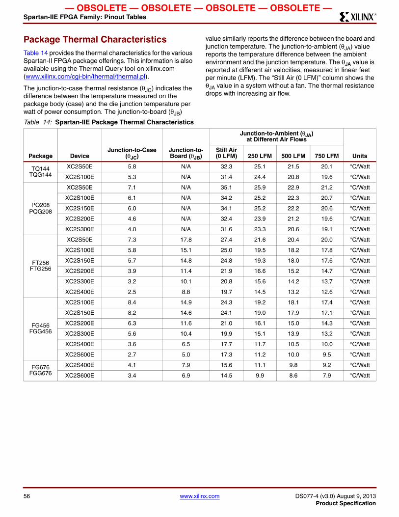
Spartan-IIE FPGA Family: Pinout TablesR
— OBSOLETE — OBSOLETE — OBSOLETE — OBSOLETE —
Package Thermal CharacteristicsTable 14 provides the thermal characteristics for the various Spartan-II FPGA package offerings. This information is also available using the Thermal Query tool on xilinx.com (www.xilinx.com/cgi-bin/thermal/thermal.pl).
The junction-to-case thermal resistance (θJC) indicates the difference between the temperature measured on the package body (case) and the die junction temperature per watt of power consumption. The junction-to-board (θJB)
value similarly reports the difference between the board and junction temperature. The junction-to-ambient (θJA) value reports the temperature difference between the ambient environment and the junction temperature. The θJA value is reported at different air velocities, measured in linear feet per minute (LFM). The “Still Air (0 LFM)” column shows the θJA value in a system without a fan. The thermal resistance drops with increasing air flow.
Table 14: Spartan-IIE Package Thermal Characteristics
Package DeviceJunction-to-Case
(θJC)Junction-to-Board (θJB)
Junction-to-Ambient (θJA) at Different Air Flows
UnitsStill Air (0 LFM) 250 LFM 500 LFM 750 LFM
TQ144TQG144
XC2S50E 5.8 N/A 32.3 25.1 21.5 20.1 °C/Watt
XC2S100E 5.3 N/A 31.4 24.4 20.8 19.6 °C/Watt
PQ208PQG208
XC2S50E 7.1 N/A 35.1 25.9 22.9 21.2 °C/Watt
XC2S100E 6.1 N/A 34.2 25.2 22.3 20.7 °C/Watt
XC2S150E 6.0 N/A 34.1 25.2 22.2 20.6 °C/Watt
XC2S200E 4.6 N/A 32.4 23.9 21.2 19.6 °C/Watt
XC2S300E 4.0 N/A 31.6 23.3 20.6 19.1 °C/Watt
FT256FTG256
XC2S50E 7.3 17.8 27.4 21.6 20.4 20.0 °C/Watt
XC2S100E 5.8 15.1 25.0 19.5 18.2 17.8 °C/Watt
XC2S150E 5.7 14.8 24.8 19.3 18.0 17.6 °C/Watt
XC2S200E 3.9 11.4 21.9 16.6 15.2 14.7 °C/Watt
XC2S300E 3.2 10.1 20.8 15.6 14.2 13.7 °C/Watt
XC2S400E 2.5 8.8 19.7 14.5 13.2 12.6 °C/Watt
FG456FGG456
XC2S100E 8.4 14.9 24.3 19.2 18.1 17.4 °C/Watt
XC2S150E 8.2 14.6 24.1 19.0 17.9 17.1 °C/Watt
XC2S200E 6.3 11.6 21.0 16.1 15.0 14.3 °C/Watt
XC2S300E 5.6 10.4 19.9 15.1 13.9 13.2 °C/Watt
XC2S400E 3.6 6.5 17.7 11.7 10.5 10.0 °C/Watt
XC2S600E 2.7 5.0 17.3 11.2 10.0 9.5 °C/Watt
FG676FGG676
XC2S400E 4.1 7.9 15.6 11.1 9.8 9.2 °C/Watt
XC2S600E 3.4 6.9 14.5 9.9 8.6 7.9 °C/Watt
56 www.xilinx.com DS077-4 (v3.0) August 9, 2013Product Specification

Spartan-IIE FPGA Family: Pinout TablesR
— OBSOLETE — OBSOLETE — OBSOLETE — OBSOLETE —
Low Voltage Differential Signals (LVDS and LVPECL)The Spartan-IIE family features low-voltage differential sig-naling (LVDS and LVPECL). Each signal utilizes two pins on the Spartan-IIE device, known as differential pin pairs. Each differential pin pair has a Positive (P) and a Negative (N) pin. These pairs are labeled in the following manner.
I/O, L#[P/N][-/_Y/_YY]
where
L = LVDS or LVPECL pin
# = Pin pair number
P = Positive
N = Negative
_Y = Asynchronous output allowed (device-dependent)
_YY = Asynchronous output allowed (all devices)
Synchronous or AsynchronousI/O pins for differential signals can either be synchronous or asynchronous, input or output. Differential signaling requires the pins of each pair to switch simultaneously. If the output signals driving the pins are from IOB flip-flops, they are synchronous. If the signals driving the pins are from internal logic, they are asynchronous, and therefore more care must be taken that they are simultaneous. Any differ-ential pairs can be used for synchronous input and output signals as well as asynchronous input signals.
However, only the differential pairs with the _Y or _YY suffix can be used for asynchronous output signals.
Asynchronous Output Pad Name DesignationBecause of differences between densities, the differential pairs that can be used for asynchronous outputs vary by device. The pairs that are available in all densities for a given package have the _YY suffix. These pins should be used for differential asynchronous outputs if the design may later move to a different density. All other differential pairs that can be used for asynchronous outputs have the _Y suf-fix.
To simplify the following tables, the "Pad Name" column shows the part of the name that is common across densi-ties. The "Pad Name" column leaves out the _Y suffix and the "LVDS Asynchronous Output Option" column indicates the densities that allow asynchronous outputs for LVDS or LVPECL on the given pin.
DLL PinsPins labeled "I/O (DLL)" can be used as general-purpose I/O or as inputs to the DLL. Adjacent DLL pins form a differ-ential pair. They reside in two different banks, so if they are outputs the VCCO level must be the same for both banks. Each DLL pin can also be paired with the adjacent GCK clock pin for a differential clock input. The "I/O (DLL)" pin always becomes the N terminal when paired with GCK, even if it is labeled "P" for its pairing with the adjacent DLL pin.
VREF PinsPins labeled "I/O, VREF" can be used as either an I/O or a VREF pin. If any I/O pin within the bank requires a VREF input, all the VREF pins in the bank must be connected to the same voltage. See the I/O banking rules in the Func-tional Description module for more detail. If no pin in a given bank requires VREF, then that bank's VREF pins can be used as general I/O.
To simplify the following tables, the "Pad Name" column shows the part of the name that is common across densi-ties. When VREF is only available in limited densities, the "Pad Name" column leaves out the VREF designation and the "VREF Option" column indicates the densities that pro-vide VREF on the given pin.
VCCO BanksIn the TQ144 and PQ208 packages, the eight banks have VCCO connected together. Thus, only one VCCO is allowed in these packages, although different VREF values are allowed in each of the eight banks. See I/O Banking.
Available Differential Pairs According to Package Type
Device TQ144 PQ208 FT256 FG456 FG676
XC2S50E 28 50 83 - -
XC2S100E 28 50 83 86 -
XC2S150E - 50 83 114 -
XC2S200E - 50 83 120 -
XC2S300E - 50 83 120 -
XC2S400E - - 83 120 172
XC2S600E - - - 120 205
DS077-4 (v3.0) August 9, 2013 www.xilinx.com 57Product Specification

Spartan-IIE FPGA Family: Pinout TablesR
— OBSOLETE — OBSOLETE — OBSOLETE — OBSOLETE —
Pinout TablesThe following device-specific pinout tables include all pack-ages available for each Spartan-IIE device. They follow the pad locations around the die. In the TQ144 package, all VCCO pins must be connected to the same voltage.
TQ144 Pinouts (XC2S50E and XC2S100E)
Pad Name
Pin
LVDS Async. Output Option
VREF OptionFunction Bank
GND - P1 - -
TMS - P2 - -
I/O 7 P3 - -
I/O 7 P4 - -
I/O, VREF Bank 7
7 P5 - All
I/O 7 P6 - -
I/O, L27P 7 P7 XC2S50E XC2S100E
I/O, L27N 7 P8 XC2S50E -
GND - P9 - -
I/O, L26P_YY 7 P10 All -
I/O, L26N_YY 7 P11 All -
I/O, VREF Bank 7, L25P
7 P12 XC2S50E All
I/O, L25N 7 P13 XC2S50E -
I/O 7 P14 - -
I/O (IRDY) 7 P15 - -
GND - P16 - -
VCCO - P17 - -
I/O (TRDY) 6 P18 - -
VCCINT - P19 - -
I/O 6 P20 - -
I/O, L24P 6 P21 XC2S50E -
I/O, VREF Bank 6, L24N
6 P22 XC2S50E All
I/O, L23P_YY 6 P23 All -
I/O, L23N_YY 6 P24 All -
GND - P25 - -
I/O, L22P 6 P26 XC2S50E -
I/O, L22N 6 P27 XC2S50E XC2S100E
I/O 6 P28 - -
I/O, VREF Bank 6
6 P29 - All
I/O 6 P30 - -
I/O, L21P_YY 6 P31 All -
I/O, L21N_YY 6 P32 All -
M1 - P33 - -
GND - P34 - -
M0 - P35 - -
VCCO - P36 - -
M2 - P37 - -
I/O, L20N_YY 5 P38 All -
I/O, L20P_YY 5 P39 All -
I/O 5 P40 - -
I/O, VREF Bank 5
5 P41 - All
I/O 5 P42 - -
I/O, L19N_YY 5 P43 All XC2S100E
I/O, L19P_YY 5 P44 All -
GND - P45 - -
VCCINT - P46 - -
I/O, L18N_YY 5 P47 All -
I/O, L18P_YY 5 P48 All -
I/O, VREF Bank 5
5 P49 - All
I/O (DLL), L17N 5 P50 - -
VCCINT - P51 - -
GCK1, I 5 P52 - -
VCCO 5 P53 - -
GND - P54 - -
GCK0, I 4 P55 - -
TQ144 Pinouts (XC2S50E and XC2S100E) (Continued)
Pad Name
Pin
LVDS Async. Output Option
VREF OptionFunction Bank
58 www.xilinx.com DS077-4 (v3.0) August 9, 2013Product Specification

Spartan-IIE FPGA Family: Pinout TablesR
— OBSOLETE — OBSOLETE — OBSOLETE — OBSOLETE —
I/O (DLL), L17P 4 P56 - -
I/O 4 P57 - -
I/O, VREF Bank 4
4 P58 - All
I/O, L16N_YY 4 P59 All -
I/O, L16P_YY 4 P60 All -
VCCINT - P61 - -
GND - P62 - -
I/O, L15N_YY 4 P63 All -
I/O, L15P_YY 4 P64 All XC2S100E
I/O 4 P65 - -
I/O, VREF Bank 4
4 P66 - All
I/O 4 P67 - -
I/O, L14N_YY 4 P68 All -
I/O, L14P_YY 4 P69 All -
GND - P70 - -
DONE 3 P71 - -
VCCO - P72 - -
PROGRAM - P73 - -
I/O (INIT), L13N_YY
3 P74 All -
I/O (D7), L13P_YY
3 P75 All -
I/O 3 P76 - -
I/O, VREF Bank 3
3 P77 - All
I/O 3 P78 - -
I/O, L12N 3 P79 XC2S50E XC2S100E
I/O (D6), L12P 3 P80 XC2S50E -
GND - P81 - -
I/O (D5), L11N_YY
3 P82 All -
I/O, L11P_YY 3 P83 All -
I/O 3 P84 - -
TQ144 Pinouts (XC2S50E and XC2S100E) (Continued)
Pad Name
Pin
LVDS Async. Output Option
VREF OptionFunction Bank
I/O, VREF Bank 3, L10N
3 P85 XC2S50E All
I/O (D4), L10P 3 P86 XC2S50E -
I/O 3 P87 - -
VCCINT - P88 - -
I/O (TRDY) 3 P89 - -
VCCO - P90 - -
GND - P91 - -
I/O (IRDY) 2 P92 - -
I/O 2 P93 - -
I/O (D3), L9N 2 P94 XC2S50E -
I/O, VREF Bank 2, L9P
2 P95 XC2S50E All
I/O 2 P96 - -
I/O, L8N_YY 2 P97 All -
I/O (D2), L8P_YY
2 P98 All -
GND - P99 - -
I/O (D1), L7N 2 P100 XC2S50E -
I/O, L7P 2 P101 XC2S50E XC2S100E
I/O 2 P102 - -
I/O, VREF Bank 2
2 P103 - All
I/O 2 P104 - -
I/O (DIN, D0), L6N_YY
2 P105 All -
I/O (DOUT, BUSY), L6P_YY
2 P106 All -
CCLK 2 P107 - -
VCCO - P108 - -
TDO 2 P109 - -
GND - P110 - -
TDI - P111 - -
TQ144 Pinouts (XC2S50E and XC2S100E) (Continued)
Pad Name
Pin
LVDS Async. Output Option
VREF OptionFunction Bank
DS077-4 (v3.0) August 9, 2013 www.xilinx.com 59Product Specification

Spartan-IIE FPGA Family: Pinout TablesR
— OBSOLETE — OBSOLETE — OBSOLETE — OBSOLETE —
I/O (CS), L5P_YY
1 P112 All -
I/O (WRITE), L5N_YY
1 P113 All -
I/O 1 P114 - -
I/O, VREF Bank 1
1 P115 - All
I/O 1 P116 - -
I/O, L4P_YY 1 P117 All XC2S100E
I/O, L4N_YY 1 P118 All -
GND - P119 - -
VCCINT - P120 - -
I/O, L3P_YY 1 P121 All -
I/O, L3N_YY 1 P122 All -
I/O, VREF Bank 1
1 P123 - All
I/O 1 P124 - -
I/O (DLL), L2P 1 P125 - -
GCK2, I 1 P126 - -
GND - P127 - -
VCCO - P128 - -
GCK3, I 0 P129 - -
VCCINT - P130 - -
I/O (DLL), L2N 0 P131 - -
I/O, VREF Bank 0
0 P132 - All
I/O, L1P_YY 0 P133 All -
I/O, L1N_YY 0 P134 All -
VCCINT - P135 - -
GND - P136 - -
I/O, L0P_YY 0 P137 All -
I/O, L0N_YY 0 P138 All XC2S100E
TQ144 Pinouts (XC2S50E and XC2S100E) (Continued)
Pad Name
Pin
LVDS Async. Output Option
VREF OptionFunction Bank
I/O 0 P139 - -
I/O, VREF Bank 0
0 P140 - All
I/O 0 P141 - -
I/O 0 P142 - -
TCK - P143 - -
VCCO - P144 - -
TQ144 Differential Clock Pins
Clock Bank
P N
Pin Name Pin Name
GCK0 4 P55 GCK0, I P56 I/O (DLL), L17P
GCK1 5 P52 GCK1, I P50 I/O (DLL), L17N
GCK2 1 P126 GCK2, I P125 I/O (DLL), L2P
GCK3 0 P129 GCK3, I P131 I/O (DLL), L2N
TQ144 Pinouts (XC2S50E and XC2S100E) (Continued)
Pad Name
Pin
LVDS Async. Output Option
VREF OptionFunction Bank
60 www.xilinx.com DS077-4 (v3.0) August 9, 2013Product Specification
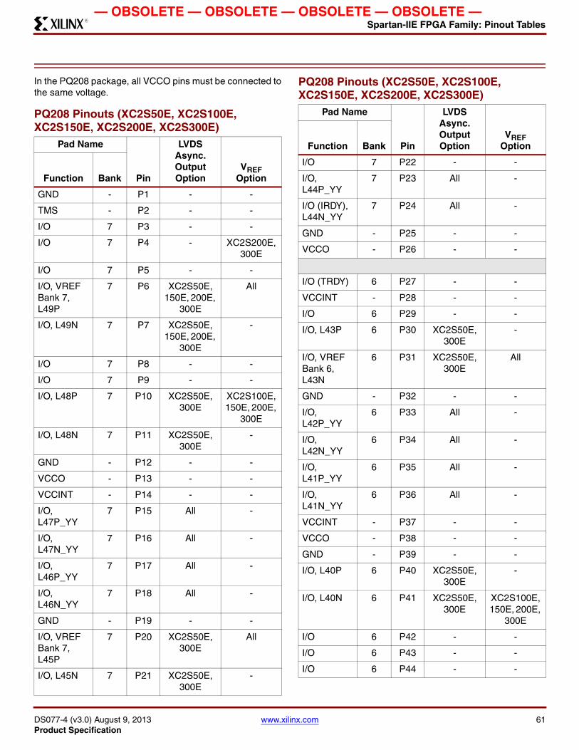
Spartan-IIE FPGA Family: Pinout TablesR
— OBSOLETE — OBSOLETE — OBSOLETE — OBSOLETE —
In the PQ208 package, all VCCO pins must be connected to the same voltage.
PQ208 Pinouts (XC2S50E, XC2S100E, XC2S150E, XC2S200E, XC2S300E)
Pad Name
Pin
LVDS Async. Output Option
VREF OptionFunction Bank
GND - P1 - -
TMS - P2 - -
I/O 7 P3 - -
I/O 7 P4 - XC2S200E, 300E
I/O 7 P5 - -
I/O, VREF Bank 7, L49P
7 P6 XC2S50E, 150E, 200E,
300E
All
I/O, L49N 7 P7 XC2S50E, 150E, 200E,
300E
-
I/O 7 P8 - -
I/O 7 P9 - -
I/O, L48P 7 P10 XC2S50E, 300E
XC2S100E, 150E, 200E,
300E
I/O, L48N 7 P11 XC2S50E, 300E
-
GND - P12 - -
VCCO - P13 - -
VCCINT - P14 - -
I/O, L47P_YY
7 P15 All -
I/O, L47N_YY
7 P16 All -
I/O, L46P_YY
7 P17 All -
I/O, L46N_YY
7 P18 All -
GND - P19 - -
I/O, VREF Bank 7, L45P
7 P20 XC2S50E, 300E
All
I/O, L45N 7 P21 XC2S50E, 300E
-
I/O 7 P22 - -
I/O, L44P_YY
7 P23 All -
I/O (IRDY), L44N_YY
7 P24 All -
GND - P25 - -
VCCO - P26 - -
I/O (TRDY) 6 P27 - -
VCCINT - P28 - -
I/O 6 P29 - -
I/O, L43P 6 P30 XC2S50E, 300E
-
I/O, VREF Bank 6, L43N
6 P31 XC2S50E, 300E
All
GND - P32 - -
I/O, L42P_YY
6 P33 All -
I/O, L42N_YY
6 P34 All -
I/O, L41P_YY
6 P35 All -
I/O, L41N_YY
6 P36 All -
VCCINT - P37 - -
VCCO - P38 - -
GND - P39 - -
I/O, L40P 6 P40 XC2S50E, 300E
-
I/O, L40N 6 P41 XC2S50E, 300E
XC2S100E, 150E, 200E,
300E
I/O 6 P42 - -
I/O 6 P43 - -
I/O 6 P44 - -
PQ208 Pinouts (XC2S50E, XC2S100E, XC2S150E, XC2S200E, XC2S300E)
Pad Name
Pin
LVDS Async. Output Option
VREF OptionFunction Bank
DS077-4 (v3.0) August 9, 2013 www.xilinx.com 61Product Specification

Spartan-IIE FPGA Family: Pinout TablesR
— OBSOLETE — OBSOLETE — OBSOLETE — OBSOLETE —
I/O, VREF Bank 6, L39P
6 P45 XC2S100E, 150E
All
I/O, L39N 6 P46 XC2S100E, 150E
-
I/O 6 P47 - XC2S200E, 300E
I/O, L38P_YY
6 P48 All -
I/O, L38N_YY
6 P49 All -
M1 - P50 - -
GND - P51 - -
M0 - P52 - -
VCCO - P53 - -
M2 - P54 - -
I/O, L37N_YY
5 P55 All -
I/O, L37P_YY
5 P56 All -
I/O 5 P57 - XC2S200E, 300E
I/O 5 P58 - -
I/O, VREF Bank 5, L36N_YY
5 P59 All All
I/O, L36P_YY
5 P60 All -
I/O, L35N 5 P61 XC2S50E, 100E, 300E
-
I/O, L35P 5 P62 XC2S50E, 100E, 300E
-
I/O, L34N 5 P63 XC2S50E, 100E, 200E,
300E
XC2S100E, 150E, 200E,
300E
I/O, L34P 5 P64 XC2S50E, 100E, 200E,
300E
-
GND - P65 - -
PQ208 Pinouts (XC2S50E, XC2S100E, XC2S150E, XC2S200E, XC2S300E)
Pad Name
Pin
LVDS Async. Output Option
VREF OptionFunction Bank
VCCO - P66 - -
VCCINT - P67 - -
I/O, L33N 5 P68 XC2S50E, 100E, 200E,
300E
-
I/O, L33P 5 P69 XC2S50E, 100E, 200E,
300E
-
I/O 5 P70 - -
I/O, L32N 5 P71 XC2S100E, 150E
-
GND - P72 - -
I/O, VREF Bank 5, L32P
5 P73 XC2S100E, 150E
All
I/O 5 P74 - -
I/O (DLL), L31N
5 P75 - -
VCCINT - P76 - -
GCK1, I 5 P77 - -
VCCO - P78 - -
GND - P79 - -
GCK0, I 4 P80 - -
I/O (DLL), L31P
4 P81 - -
I/O 4 P82 - -
I/O, L30N 4 P83 XC2S50E, 200E, 300E
-
I/O, VREF Bank 4, L30P
4 P84 XC2S50E, 200E, 300E
All
GND - P85 - -
I/O, L29N 4 P86 XC2S50E, 200E, 300E
-
I/O, L29P 4 P87 XC2S50E, 200E, 300E
-
I/O, L28N 4 P88 XC2S50E, 100E, 200E,
300E
-
PQ208 Pinouts (XC2S50E, XC2S100E, XC2S150E, XC2S200E, XC2S300E)
Pad Name
Pin
LVDS Async. Output Option
VREF OptionFunction Bank
62 www.xilinx.com DS077-4 (v3.0) August 9, 2013Product Specification

Spartan-IIE FPGA Family: Pinout TablesR
— OBSOLETE — OBSOLETE — OBSOLETE — OBSOLETE —
I/O, L28P 4 P89 XC2S50E, 100E, 200E,
300E
-
VCCINT - P90 - -
VCCO - P91 - -
GND - P92 - -
I/O, L27N 4 P93 XC2S50E, 100E, 200E,
300E
-
I/O, L27P 4 P94 XC2S50E, 100E, 200E,
300E
XC2S100E, 150E, 200E,
300E
I/O 4 P95 - -
I/O 4 P96 - -
I/O, L26N_YY
4 P97 All -
I/O, VREF Bank 4, L26P_YY
4 P98 All All
I/O 4 P99 - -
I/O 4 P100 - XC2S200E, 300E
I/O, L25N_YY
4 P101 All -
I/O, L25P_YY
4 P102 All -
GND - P103 - -
DONE 3 P104 - -
VCCO - P105 - -
PROGRAM - P106 - -
I/O (INIT), L24N_YY
3 P107 All -
I/O (D7), L24P_YY
3 P108 All -
I/O 3 P109 - XC2S200E, 300E
I/O 3 P110 - -
PQ208 Pinouts (XC2S50E, XC2S100E, XC2S150E, XC2S200E, XC2S300E)
Pad Name
Pin
LVDS Async. Output Option
VREF OptionFunction Bank
I/O, VREF Bank 3, L23N
3 P111 XC2S50E, 150E, 200E,
300E
All
I/O, L23P 3 P112 XC2S50E, 150E, 200E,
300E
-
I/O 3 P113 - -
I/O 3 P114 - -
I/O, L22N 3 P115 XC2S50E, 300E
XC2S100E, 150E, 200E,
300E
I/O (D6), L22P
3 P116 XC2S50E, 300E
-
GND - P117 - -
VCCO - P118 - -
VCCINT - P119 - -
I/O (D5), L21N_YY
3 P120 All -
I/O, L21P_YY
3 P121 All -
I/O, L20N_YY
3 P122 All -
I/O, L20P_YY
3 P123 All -
GND - P124 - -
I/O, VREF Bank 3, L19N
3 P125 XC2S50E, 300E
All
I/O (D4), L19P
3 P126 XC2S50E, 300E
-
I/O 3 P127 - -
VCCINT - P128 - -
I/O (TRDY) 3 P129 - -
VCCO - P130 - -
GND - P131 - -
I/O (IRDY), L18N_YY
2 P132 All -
I/O, L18P_YY
2 P133 All -
PQ208 Pinouts (XC2S50E, XC2S100E, XC2S150E, XC2S200E, XC2S300E)
Pad Name
Pin
LVDS Async. Output Option
VREF OptionFunction Bank
DS077-4 (v3.0) August 9, 2013 www.xilinx.com 63Product Specification

Spartan-IIE FPGA Family: Pinout TablesR
— OBSOLETE — OBSOLETE — OBSOLETE — OBSOLETE —
I/O 2 P134 - -
I/O (D3), L17N
2 P135 XC2S50E, 300E
-
I/O, VREF Bank 2, L17P
2 P136 XC2S50E, 300E
All
GND - P137 - -
I/O, L16N_YY
2 P138 All -
I/O, L16P_YY
2 P139 All -
I/O, L15N_YY
2 P140 All -
I/O (D2), L15P_YY
2 P141 All -
VCCINT - P142 - -
VCCO - P143 - -
GND - P144 - -
I/O (D1), L14N
2 P145 XC2S50E, 300E
-
I/O, L14P 2 P146 XC2S50E, 300E
XC2S100E, 150E, 200E,
300E
I/O 2 P147 - -
I/O 2 P148 - -
I/O 2 P149 - -
I/O, VREF Bank 2, L13N
2 P150 XC2S100E, 150E
All
I/O, L13P 2 P151 XC2S100E, 150E
-
I/O 2 P152 - XC2S200E, 300E
I/O (DIN, D0), L12N_YY
2 P153 All -
I/O (DOUT, BUSY), L12P_YY
2 P154 All -
CCLK 2 P155 - -
PQ208 Pinouts (XC2S50E, XC2S100E, XC2S150E, XC2S200E, XC2S300E)
Pad Name
Pin
LVDS Async. Output Option
VREF OptionFunction Bank
VCCO - P156 - -
TDO 2 P157 - -
GND - P158 - -
TDI - P159 - -
I/O (CS), L11P_YY
1 P160 All -
I/O (WRITE), L11N_YY
1 P161 All -
I/O 1 P162 - XC2S200E, 300E
I/O 1 P163 - -
I/O, VREF Bank 1, L10P_YY
1 P164 All All
I/O, L10N_YY
1 P165 All -
I/O 1 P166 - -
I/O 1 P167 - -
I/O, L9P 1 P168 XC2S50E, 100E, 200E,
300E
XC2S100E, 150E, 200E,
300E
I/O, L9N 1 P169 XC2S50E, 100E, 200E,
300E
-
GND - P170 - -
VCCO - P171 - -
VCCINT - P172 - -
I/O, L8P 1 P173 XC2S50E, 100E, 200E,
300E
-
I/O, L8N 1 P174 XC2S50E, 100E, 200E,
300E
-
I/O, L7P 1 P175 XC2S50E, 200E, 300E
-
I/O, L7N 1 P176 XC2S50E, 200E, 300E
-
GND - P177 - -
PQ208 Pinouts (XC2S50E, XC2S100E, XC2S150E, XC2S200E, XC2S300E)
Pad Name
Pin
LVDS Async. Output Option
VREF OptionFunction Bank
64 www.xilinx.com DS077-4 (v3.0) August 9, 2013Product Specification

Spartan-IIE FPGA Family: Pinout TablesR
— OBSOLETE — OBSOLETE — OBSOLETE — OBSOLETE —
I/O, VREF Bank 1, L6P
1 P178 XC2S50E, 200E, 300E
All
I/O, L6N 1 P179 XC2S50E, 200E, 300E
-
I/O 1 P180 - -
I/O (DLL), L5P
1 P181 - -
GCK2, I 1 P182 - -
GND - P183 - -
VCCO - P184 - -
GCK3, I 0 P185 - -
VCCINT - P186 - -
I/O (DLL), L5N
0 P187 - -
I/O, L4P 0 P188 XC2S50E, 200E, 300E
-
I/O, VREF Bank 0, L4N
0 P189 XC2S50E, 200E, 300E
All
GND - P190 - -
I/O, L3P 0 P191 XC2S50E, 200E, 300E
-
I/O, L3N 0 P192 XC2S50E, 200E, 300E
-
I/O, L2P 0 P193 XC2S50E, 100E, 200E,
300E
-
I/O, L2N 0 P194 XC2S50E, 100E, 200E,
300E
-
VCCINT - P195 - -
VCCO - P196 - -
GND - P197 - -
I/O, L1P 0 P198 XC2S50E, 100E, 200E,
300E
-
I/O, L1N 0 P199 XC2S50E, 100E, 200E,
300E
XC2S100E, 150E, 200E,
300E
I/O 0 P200 - -
PQ208 Pinouts (XC2S50E, XC2S100E, XC2S150E, XC2S200E, XC2S300E)
Pad Name
Pin
LVDS Async. Output Option
VREF OptionFunction Bank
I/O 0 P201 - -
I/O, L0P_YY
0 P202 All -
I/O, VREF Bank 0, L0N_YY
0 P203 All All
I/O 0 P204 - -
I/O 0 P205 - XC2S200E, 300E
I/O 0 P206 - -
TCK - P207 - -
VCCO - P208 - -
PQ208 Differential Clock Pins
Clock Bank
P N
Pin Name Pin Name
GCK0 4 P80 GCK0, I P81 I/O (DLL), L31P
GCK1 5 P77 GCK1, I P75 I/O (DLL), L31N
GCK2 1 P182 GCK2, I P181 I/O (DLL), L5P
GCK3 0 P185 GCK3, I P187 I/O (DLL), L5N
PQ208 Pinouts (XC2S50E, XC2S100E, XC2S150E, XC2S200E, XC2S300E)
Pad Name
Pin
LVDS Async. Output Option
VREF OptionFunction Bank
DS077-4 (v3.0) August 9, 2013 www.xilinx.com 65Product Specification

Spartan-IIE FPGA Family: Pinout TablesR
— OBSOLETE — OBSOLETE — OBSOLETE — OBSOLETE —
FT256 Pinouts (XC2S50E, XC2S100E, XC2S150E, XC2S200E, XC2S300E, XC2S400E)
Pad Name
Pin
LVDS Async. Output Option
VREF OptionFunction Bank
TMS - B1 - -
I/O 7 D3 - -
I/O, L83P 7 C2 XC2S100E, 150E
-
I/O, L83N 7 C1 XC2S100E, 150E
XC2S200E, 300E, 400E
I/O, L82P_YY 7 D2 All -
I/O, L82N_YY 7 D1 All -
I/O, VREF Bank 7, L81P
7 E3 XC2S50E, 150E, 200E, 300E, 400E
All
I/O, L81N 7 E4 XC2S50E, 150E, 200E, 300E, 400E
-
I/O, L80P 7 E2 XC2S200E, 400E
-
I/O, L80N 7 E1 XC2S200E, 400E
-
I/O, L79P 7 F4 XC2S50E, 300E, 400E
XC2S100E, 150E, 200E, 300E, 400E
I/O, L79N 7 F3 XC2S50E, 300E, 400E
-
I/O, L78P_YY 7 F2 All -
I/O, L78N_YY 7 F1 All -
I/O, L77P 7 F5 XC2S100E, 150E
-
I/O, L77N 7 G5 XC2S100E, 150E
-
I/O, L76P_YY 7 G3 All -
I/O, L76N_YY 7 G4 All -
I/O, VREF Bank 7, L75P
7 G2 XC2S50E, 300E, 400E
All
I/O, L75N 7 G1 XC2S50E, 300E, 400E
-
I/O, L74P 7 H4 XC2S100E, 150E, 200E
-
I/O, L74N 7 H3 XC2S100E, 150E, 200E
XC2S400E
I/O, L73P_YY 7 H2 All -
I/O (IRDY), L73N_YY
7 H1 All -
I/O (TRDY) 6 J4 - -
I/O, L72P 6 J2 XC2S100E, 150E, 200E,
400E
XC2S400E
I/O, L72N 6 J3 XC2S100E, 150E, 200E,
400E
-
I/O, L71P 6 J1 XC2S50E, 300E, 400E
-
I/O, VREF Bank 6, L71N
6 K1 XC2S50E, 300E, 400E
All
I/O, L70P_YY 6 K2 All -
I/O, L70N_YY 6 K3 All -
I/O, L69P 6 L1 XC2S100E, 150E, 400E
-
I/O, L69N 6 L2 XC2S100E, 150E, 400E
-
I/O, L68P_YY 6 K4 All -
I/O, L68N_YY 6 K5 All -
I/O, L67P 6 L3 XC2S50E, 300E, 400E
-
I/O, L67N 6 M2 XC2S50E, 300E, 400E
XC2S100E, 150E, 200E, 300E, 400E
I/O, L66P 6 M1 XC2S150E, 200E, 400E
-
I/O, L66N 6 N1 XC2S150E, 200E, 400E
-
FT256 Pinouts (XC2S50E, XC2S100E, XC2S150E, XC2S200E, XC2S300E, XC2S400E) (Continued)
Pad Name
Pin
LVDS Async. Output Option
VREF OptionFunction Bank
66 www.xilinx.com DS077-4 (v3.0) August 9, 2013Product Specification

Spartan-IIE FPGA Family: Pinout TablesR
— OBSOLETE — OBSOLETE — OBSOLETE — OBSOLETE —
I/O, L65P 6 L4 XC2S50E, 150E, 200E, 300E, 400E
-
I/O, VREF Bank 6, L65N
6 L5 XC2S50E, 150E, 200E, 300E, 400E
All
I/O, L64P_YY 6 M3 All -
I/O, L64N_YY 6 M4 All -
I/O, L63P 6 N2 XC2S100E, 200E, 300E
-
I/O, L63N 6 N3 XC2S100E, 200E, 300E
XC2S200E, 300E, 400E
I/O, L62P_YY 6 P1 All -
I/O, L62N_YY 6 P2 All -
M1 - R1 - -
M0 - T2 - -
M2 - R3 - -
I/O, L61N_YY 5 P4 All -
I/O, L61P_YY 5 R4 All -
I/O, L60N 5 T3 XC2S50E, 100E, 200E, 300E, 400E
XC2S200E, 300E, 400E
I/O, L60P 5 T4 XC2S50E, 100E, 200E, 300E, 400E
-
I/O, L59N_YY 5 N5 All -
I/O, L59P_YY 5 P5 All -
I/O, VREF Bank 5, L58N_YY
5 R5 All All
I/O, L58P_YY 5 T5 All -
I/O, L57N 5 N6 XC2S50E, 100E, 150E,
300E
-
FT256 Pinouts (XC2S50E, XC2S100E, XC2S150E, XC2S200E, XC2S300E, XC2S400E) (Continued)
Pad Name
Pin
LVDS Async. Output Option
VREF OptionFunction Bank
I/O, L57P 5 P6 XC2S50E, 100E, 150E,
300E
-
I/O, L56N 5 R6 XC2S50E, 100E, 200E, 300E, 400E
XC2S100E, 150E, 200E, 300E, 400E
I/O, L56P 5 T6 XC2S50E, 100E, 200E, 300E, 400E
-
I/O, L55N 5 M6 XC2S50E, 100E, 200E, 300E, 400E
-
I/O, L55P 5 N7 XC2S50E, 100E, 200E, 300E, 400E
-
I/O 5 P7 - -
I/O, L54N 5 R7 XC2S50E, 200E, 300E,
400E
-
I/O, L54P 5 T7 XC2S50E, 200E, 300E,
400E
-
I/O, VREF Bank 5, L53N
5 M7 XC2S50E, 200E, 300E,
400E
All
I/O, L53P 5 N8 XC2S50E, 200E, 300E,
400E
-
I/O 5 P8 - XC2S400E
I/O (DLL), L52N
5 R8 - -
GCK1, I 5 T8 - -
GCK0, I 4 T9 - -
I/O (DLL), L52P
4 R9 - -
I/O, L51N 4 P9 XC2S50E, 150E, 200E,
400E
XC2S400E
FT256 Pinouts (XC2S50E, XC2S100E, XC2S150E, XC2S200E, XC2S300E, XC2S400E) (Continued)
Pad Name
Pin
LVDS Async. Output Option
VREF OptionFunction Bank
DS077-4 (v3.0) August 9, 2013 www.xilinx.com 67Product Specification

Spartan-IIE FPGA Family: Pinout TablesR
— OBSOLETE — OBSOLETE — OBSOLETE — OBSOLETE —
I/O, L51P 4 N9 XC2S50E, 150E, 200E,
400E
-
I/O, L50N 4 T10 XC2S50E, 200E, 300E,
400E
-
I/O, VREF Bank 4, L50P
4 R10 XC2S50E, 200E, 300E,
400E
All
I/O, L49N 4 P10 XC2S50E, 200E, 300E,
400E
-
I/O, L49P 4 R11 XC2S50E, 200E, 300E,
400E
-
I/O 4 T11 - -
I/O, L48N 4 N10 XC2S50E, 100E, 200E, 300E, 400E
-
I/O, L48P 4 M10 XC2S50E, 100E, 200E, 300E, 400E
-
I/O, L47N 4 P11 XC2S50E, 100E, 200E, 300E, 400E
-
I/O, L47P 4 R12 XC2S50E, 100E, 200E, 300E, 400E
XC2S100E, 150E, 200E, 300E, 400E
I/O, L46N 4 T12 XC2S50E, 100E, 150E,
300E
-
I/O, L46P 4 T13 XC2S50E, 100E, 150E,
300E
-
I/O, L45N_YY 4 N11 All -
I/O, VREF Bank 4, L45P_YY
4 M11 All All
I/O, L44N_YY 4 P12 All -
I/O, L44P_YY 4 N12 All -
FT256 Pinouts (XC2S50E, XC2S100E, XC2S150E, XC2S200E, XC2S300E, XC2S400E) (Continued)
Pad Name
Pin
LVDS Async. Output Option
VREF OptionFunction Bank
I/O, L43N 4 R13 XC2S50E, 150E
XC2S200E, 300E, 400E
I/O, L43P 4 P13 XC2S50E, 150E
-
I/O, L42N_YY 4 T14 All -
I/O, L42P_YY 4 R14 All -
DONE 3 T15 - -
PROGRAM - R16 - -
I/O (INIT), L41N_YY
3 P15 All -
I/O (D7), L41P_YY
3 P16 All -
I/O, L40N 3 N15 XC2S100E, 150E, 400E
-
I/O, L40P 3 N16 XC2S100E, 150E, 400E
XC2S200E, 300E, 400E
I/O, L39N 3 N14 XC2S50E, 100E, 150E,
200E, 300E(1)
-
I/O, L39P 3 M14 XC2S50E, 100E, 150E,
200E, 300E(1)
-
I/O, VREF Bank 3, L38N
3 M15 XC2S50E, 150E, 200E, 300E, 400E
All
I/O, L38P 3 M16 XC2S50E, 150E, 200E, 300E, 400E
-
I/O(2) 3 M13 - -
I/O(2) 3 L14 - -
I/O, L36N 3 L15 XC2S50E, 300E, 400E
XC2S100E, 150E, 200E, 300E, 400E
I/O (D6), L36P 3 L16 XC2S50E, 300E, 400E
-
FT256 Pinouts (XC2S50E, XC2S100E, XC2S150E, XC2S200E, XC2S300E, XC2S400E) (Continued)
Pad Name
Pin
LVDS Async. Output Option
VREF OptionFunction Bank
68 www.xilinx.com DS077-4 (v3.0) August 9, 2013Product Specification

Spartan-IIE FPGA Family: Pinout TablesR
— OBSOLETE — OBSOLETE — OBSOLETE — OBSOLETE —
I/O (D5), L35N_YY
3 L13 All -
I/O, L35P_YY 3 K14 All -
I/O, L34N 3 K15 XC2S100E, 150E, 400E
-
I/O, L34P 3 K16 XC2S100E, 150E, 400E
-
I/O, L33N 3 L12 XC2S50E, 100E, 150E,
200E, 300E(1)
-
I/O, L33P 3 K12 XC2S50E, 100E, 150E,
200E, 300E(1)
-
I/O, VREF Bank 3, L32N
3 K13 XC2S50E, 300E, 400E
All
I/O (D4), L32P 3 J14 XC2S50E, 300E, 400E
-
I/O, L31N 3 J15 XC2S100E, 150E, 200E,
400E
-
I/O, L31P 3 J16 XC2S100E, 150E, 200E,
400E
XC2S400E
I/O (TRDY) 3 J13 - -
I/O (IRDY), L30N_YY
2 H16 All -
I/O, L30P_YY 2 G16 All -
I/O, L29N 2 H14 XC2S100E, 150E, 200E,
400E
XC2S400E
I/O, L29P 2 H15 XC2S100E, 150E, 200E,
400E
-
I/O (D3), L28N 2 G15 XC2S50E, 300E, 400E
-
FT256 Pinouts (XC2S50E, XC2S100E, XC2S150E, XC2S200E, XC2S300E, XC2S400E) (Continued)
Pad Name
Pin
LVDS Async. Output Option
VREF OptionFunction Bank
I/O, VREF Bank 2, L28P
2 F16 XC2S50E, 300E, 400E
All
I/O, L27N 2 H13 XC2S50E, 100E, 150E,
200E, 300E(1)
-
I/O, L27P 2 G14 XC2S50E, 100E, 150E,
200E, 300E(2)
-
I/O, L26N 2 F15 XC2S100E, 150E, 400E
-
I/O, L26P 2 E16 XC2S100E, 150E, 400E
-
I/O, L25N_YY 2 G13 All -
I/O (D2), L25P_YY
2 F14 All -
I/O (D1), L24N 2 E15 XC2S50E, 300E, 400E
-
I/O, L24P 2 D16 XC2S50E, 300E, 400E
XC2S100E, 150E, 200E, 300E, 400E
I/O, L23N 2 F13 XC2S150E, 200E, 400E
-
I/O, L23P 2 E14 XC2S150E, 200E, 400E
-
I/O, L22N 2 D15 XC2S50E, 150E, 200E, 300E, 400E
-
I/O, VREF Bank 2, L22P
2 C16 XC2S50E, 150E, 200E, 300E, 400E
All
I/O, L21N 2 G12 XC2S50E, 100E, 200E,
300E
-
I/O, L21P 2 F12 XC2S50E, 100E, 200E,
300E
-
I/O, L20N 2 E13 XC2S100E, 200E, 300E
-
FT256 Pinouts (XC2S50E, XC2S100E, XC2S150E, XC2S200E, XC2S300E, XC2S400E) (Continued)
Pad Name
Pin
LVDS Async. Output Option
VREF OptionFunction Bank
DS077-4 (v3.0) August 9, 2013 www.xilinx.com 69Product Specification

Spartan-IIE FPGA Family: Pinout TablesR
— OBSOLETE — OBSOLETE — OBSOLETE — OBSOLETE —
I/O, L20P 2 D14 XC2S100E, 200E, 300E
XC2S200E, 300E, 400E
I/O (DIN, D0), L19N_YY
2 B16 All -
I/O (DOUT, BUSY), L19P_YY
2 C15 All -
CCLK 2 A15 - -
TDO 2 B14 - -
TDI - C13 - -
I/O (CS), L18P_YY
1 A14 All -
I/O (WRITE), L18N_YY
1 A13 All -
I/O, L17P 1 B13 XC2S50E, 100E, 200E, 300E, 400E
XC2S200E, 300E, 400E
I/O, L17N 1 C12 XC2S50E, 100E, 200E, 300E, 400E
-
I/O, L16P_YY 1 B12 All -
I/O, L16N_YY 1 A12 All -
I/O, VREF Bank 1, L15P_YY
1 D12 All All
I/O, L15N_YY 1 E11 All -
I/O, L14P 1 D11 XC2S50E, 100E, 150E,
300E
-
I/O, L14N 1 C11 XC2S50E, 100E, 150E,
300E
-
I/O, L13P 1 B11 XC2S50E, 100E, 200E, 300E, 400E
XC2S100E, 150E, 200E, 300E, 400E
I/O, L13N 1 A11 XC2S50E, 100E, 200E, 300E, 400E
-
FT256 Pinouts (XC2S50E, XC2S100E, XC2S150E, XC2S200E, XC2S300E, XC2S400E) (Continued)
Pad Name
Pin
LVDS Async. Output Option
VREF OptionFunction Bank
I/O, L12P 1 E10 XC2S50E, 100E, 200E, 300E, 400E
-
I/O, L12N 1 D10 XC2S50E, 100E, 200E, 300E, 400E
-
I/O 1 C10 - -
I/O, L11P 1 B10 XC2S50E, 200E, 300E,
400E
-
I/O, L11N 1 A10 XC2S50E, 200E, 300E,
400E
-
I/O, VREF Bank 1, L10P
1 D9 XC2S50E, 200E, 300E,
400E
All
I/O, L10N 1 C9 XC2S50E, 200E, 300E,
400E
-
I/O, L9P 1 B9 XC2S50E, 150E, 200E,
400E
-
I/O, L9N 1 A9 XC2S50E, 150E, 200E,
400E
XC2S400E
I/O (DLL), L8P 1 A8 - -
GCK2, I 1 B8 - -
GCK3, I 0 C8 - -
I/O (DLL), L8N 0 D8 - -
I/O 0 A7 - XC2S400E
I/O, L7P 0 E7 XC2S50E, 200E, 300E,
400E
-
I/O, VREF Bank 0, L7N
0 D7 XC2S50E, 200E, 300E,
400E
All
FT256 Pinouts (XC2S50E, XC2S100E, XC2S150E, XC2S200E, XC2S300E, XC2S400E) (Continued)
Pad Name
Pin
LVDS Async. Output Option
VREF OptionFunction Bank
70 www.xilinx.com DS077-4 (v3.0) August 9, 2013Product Specification

Spartan-IIE FPGA Family: Pinout TablesR
— OBSOLETE — OBSOLETE — OBSOLETE — OBSOLETE —
I/O, L6P 0 C7 XC2S50E, 200E, 300E,
400E
-
I/O, L6N 0 B7 XC2S50E, 200E, 300E,
400E
-
I/O 0 A6 - -
I/O, L5P 0 B6 XC2S50E, 100E, 200E, 300E, 400E
-
I/O, L5N 0 C6 XC2S50E, 100E, 200E, 300E, 400E
-
I/O, L4P 0 A5 XC2S50E, 100E, 200E, 300E, 400E
-
I/O, L4N 0 B5 XC2S50E, 100E, 200E, 300E, 400E
XC2S100E, 150E, 200E, 300E, 400E
I/O, L3P 0 D6 XC2S50E, 100E, 300E
-
I/O, L3N 0 E6 XC2S50E, 100E, 300E
-
I/O, L2P_YY 0 D5 All -
I/O, VREF Bank 0, L2N_YY
0 C5 All All
I/O, L1P_YY 0 B4 All -
I/O, L1N_YY 0 C4 All -
I/O, L0P_YY 0 A4 All -
I/O, L0N_YY 0 A3 All XC2S200E, 300E, 400E
I/O 0 B3 - -
TCK - A2 - -
Notes: 1. Although designated with the _YY suffix in the XC2S50E,
XC2S100E, XC2S150E, XC2S200E, and XC2S300E, these differential pairs are not asynchronous in the XC2S400E.
2. There is no pair L37.
FT256 Pinouts (XC2S50E, XC2S100E, XC2S150E, XC2S200E, XC2S300E, XC2S400E) (Continued)
Pad Name
Pin
LVDS Async. Output Option
VREF OptionFunction Bank
FT256 Differential Clock Pins
Clock Bank
P N
Pin Name Pin Name
GCK0 4 T9 GCK0, I R9 I/O (DLL), L52P
GCK1 5 T8 GCK1, I R8 I/O (DLL), L52N
GCK2 1 B8 GCK2, I A8 I/O (DLL), L8P
GCK3 0 C8 GCK3, I D8 I/O (DLL), L8N
Additional FT256 Package Pins VCCINT Pins
C3 C14 D4 D13 E5
E12 M5 M12 N4 N13
P3 P14 - - -
VCCO Bank 0 Pins
E8 F7 F8 - -
VCCO Bank 1 Pins
E9 F9 F10 - -
VCCO Bank 2 Pins
G11 H11 H12 - -
VCCO Bank 3 Pins
J11 J12 K11 - -
VCCO Bank 4 Pins
L9 L10 M9 - -
DS077-4 (v3.0) August 9, 2013 www.xilinx.com 71Product Specification
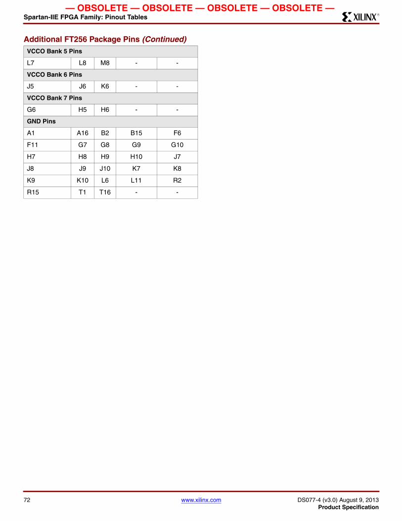
Spartan-IIE FPGA Family: Pinout TablesR
— OBSOLETE — OBSOLETE — OBSOLETE — OBSOLETE —
VCCO Bank 5 Pins
L7 L8 M8 - -
VCCO Bank 6 Pins
J5 J6 K6 - -
VCCO Bank 7 Pins
G6 H5 H6 - -
GND Pins
A1 A16 B2 B15 F6
F11 G7 G8 G9 G10
H7 H8 H9 H10 J7
J8 J9 J10 K7 K8
K9 K10 L6 L11 R2
R15 T1 T16 - -
Additional FT256 Package Pins (Continued)
72 www.xilinx.com DS077-4 (v3.0) August 9, 2013Product Specification
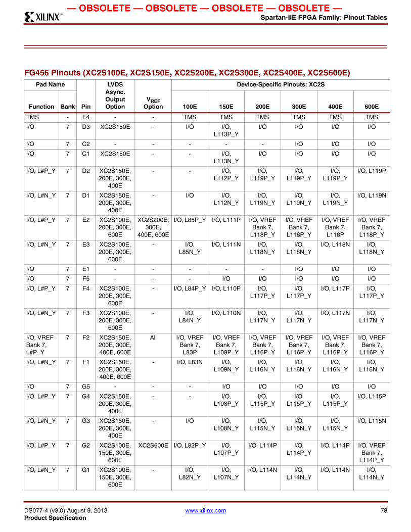
Spartan-IIE FPGA Family: Pinout TablesR
— OBSOLETE — OBSOLETE — OBSOLETE — OBSOLETE —
FG456 Pinouts (XC2S100E, XC2S150E, XC2S200E, XC2S300E, XC2S400E, XC2S600E) Pad Name
Pin
LVDS Async. Output Option
VREF Option
Device-Specific Pinouts: XC2S
Function Bank 100E 150E 200E 300E 400E 600E
TMS - E4 - - TMS TMS TMS TMS TMS TMS
I/O 7 D3 XC2S150E - I/O I/O, L113P_Y
I/O I/O I/O I/O
I/O 7 C2 - - - - - I/O I/O I/O
I/O 7 C1 XC2S150E - - I/O, L113N_Y
I/O I/O I/O I/O
I/O, L#P_Y 7 D2 XC2S150E, 200E, 300E,
400E
- - I/O, L112P_Y
I/O, L119P_Y
I/O, L119P_Y
I/O, L119P_Y
I/O, L119P
I/O, L#N_Y 7 D1 XC2S150E, 200E, 300E,
400E
- I/O I/O, L112N_Y
I/O, L119N_Y
I/O, L119N_Y
I/O, L119N_Y
I/O, L119N
I/O, L#P_Y 7 E2 XC2S100E, 200E, 300E,
600E
XC2S200E, 300E,
400E, 600E
I/O, L85P_Y I/O, L111P I/O, VREF Bank 7,
L118P_Y
I/O, VREF Bank 7,
L118P_Y
I/O, VREF Bank 7, L118P
I/O, VREF Bank 7,
L118P_Y
I/O, L#N_Y 7 E3 XC2S100E, 200E, 300E,
600E
- I/O, L85N_Y
I/O, L111N I/O, L118N_Y
I/O, L118N_Y
I/O, L118N I/O, L118N_Y
I/O 7 E1 - - - - - I/O I/O I/O
I/O 7 F5 - - - I/O I/O I/O I/O I/O
I/O, L#P_Y 7 F4 XC2S100E, 200E, 300E,
600E
- I/O, L84P_Y I/O, L110P I/O, L117P_Y
I/O, L117P_Y
I/O, L117P I/O, L117P_Y
I/O, L#N_Y 7 F3 XC2S100E, 200E, 300E,
600E
- I/O, L84N_Y
I/O, L110N I/O, L117N_Y
I/O, L117N_Y
I/O, L117N I/O, L117N_Y
I/O, VREF Bank 7, L#P_Y
7 F2 XC2S150E, 200E, 300E, 400E, 600E
All I/O, VREF Bank 7, L83P
I/O, VREF Bank 7,
L109P_Y
I/O, VREF Bank 7,
L116P_Y
I/O, VREF Bank 7,
L116P_Y
I/O, VREF Bank 7,
L116P_Y
I/O, VREF Bank 7,
L116P_Y
I/O, L#N_Y 7 F1 XC2S150E, 200E, 300E, 400E, 600E
- I/O, L83N I/O, L109N_Y
I/O, L116N_Y
I/O, L116N_Y
I/O, L116N_Y
I/O, L116N_Y
I/O 7 G5 - - - I/O I/O I/O I/O I/O
I/O, L#P_Y 7 G4 XC2S150E, 200E, 300E,
400E
- - I/O, L108P_Y
I/O, L115P_Y
I/O, L115P_Y
I/O, L115P_Y
I/O, L115P
I/O, L#N_Y 7 G3 XC2S150E, 200E, 300E,
400E
- I/O I/O, L108N_Y
I/O, L115N_Y
I/O, L115N_Y
I/O, L115N_Y
I/O, L115N
I/O, L#P_Y 7 G2 XC2S100E, 150E, 300E,
600E
XC2S600E I/O, L82P_Y I/O, L107P_Y
I/O, L114P I/O, L114P_Y
I/O, L114P I/O, VREF Bank 7,
L114P_Y
I/O, L#N_Y 7 G1 XC2S100E, 150E, 300E,
600E
- I/O, L82N_Y
I/O, L107N_Y
I/O, L114N I/O, L114N_Y
I/O, L114N I/O, L114N_Y
DS077-4 (v3.0) August 9, 2013 www.xilinx.com 73Product Specification

Spartan-IIE FPGA Family: Pinout TablesR
— OBSOLETE — OBSOLETE — OBSOLETE — OBSOLETE —
I/O 7 H5 - - - - - I/O I/O I/O
I/O, VREF Bank 7, L#P_Y
7 H3 XC2S300E, 400E, 600E
All I/O, VREF Bank 7, L81P
I/O, VREF Bank 7, L106P
I/O, VREF Bank 7, L113P
I/O, VREF Bank 7,
L113P_Y
I/O, VREF Bank 7,
L113P_Y
I/O, VREF Bank 7,
L113P_Y
I/O, L#N_Y 7 H4 XC2S300E, 400E, 600E
- I/O, L81N I/O, L106N I/O, L113N I/O, L113N_Y
I/O, L113N_Y
I/O, L113N_Y
I/O, L#P_YY
7 H2 All - I/O, L80P_YY
I/O, L105P_YY
I/O, L112P_YY
I/O, L112P_YY
I/O, L112P_YY
I/O, L112P_YY
I/O, L#N_YY
7 H1 All - I/O, L80N_YY
I/O, L105N_YY
I/O, L112N_YY
I/O, L112N_YY
I/O, L112N_YY
I/O, L112N_YY
I/O 7 J6 - - - - I/O I/O I/O I/O
I/O, L#P_Y 7 J4 XC2S150E, 200E, 300E,
400E
- - I/O, L104P_Y
I/O, L111P_Y
I/O, L111P_Y
I/O, L111P_Y
I/O, L111P
I/O, L#N_Y 7 J5 XC2S100E, 150E, 200E, 300E, 400E
- I/O, L79P_Y I/O, L104N_Y
I/O, L111N_Y
I/O, L111N_Y
I/O, L111N_Y
I/O, L111N
I/O, L#P_Y 7 J3 XC2S100E, 150E, 200E, 300E, 600E
- I/O, L79N_Y
I/O, L103P_Y
I/O, L110P_Y
I/O, L110P_Y
I/O, L110P I/O, L110P_Y
I/O, L#N_Y 7 J2 XC2S150E, 200E, 300E,
600E
- - I/O, L103N_Y
I/O, L110N_Y
I/O, L110N_Y
I/O, L110N I/O, L110N_Y
I/O 7 J1 - - - - I/O I/O I/O I/O
I/O, L#P 7 K5 XC2S100E, 150E, 200E,
300E, 600E(1)
- I/O, L78P_YY
I/O, L102P_YY
I/O, L109P_YY
I/O, L109P_YY
I/O, L109P I/O, L109P_Y
I/O, L#N 7 K6 XC2S100E, 150E, 200E,
300E, 600E(1)
- I/O, L78N_YY
I/O, L102N_YY
I/O, L109N_YY
I/O, L109N_YY
I/O, L109N I/O, L109N_Y
I/O, VREF Bank 7, L#P_Y
7 K3 XC2S300E, 400E, 600E
All I/O, VREF Bank 7, L77P
I/O, VREF Bank 7, L101P
I/O, VREF Bank 7, L108P
I/O, VREF Bank 7,
L108P_Y
I/O, VREF Bank 7,
L108P_Y
I/O, VREF Bank 7,
L108P_Y
I/O, L#N_Y 7 K4 XC2S300E, 400E, 600E
- I/O, L77N I/O, L101N I/O, L108N I/O, L108N_Y
I/O, L108N_Y
I/O, L108N_Y
I/O 7 K2 - - - - - I/O I/O I/O
I/O, L#P_Y 7 K1 XC2S300E, 400E
- - - I/O, L107P I/O, L107P_Y
I/O, L107P_Y
I/O, L107P
I/O, L#N_Y 7 L1 XC2S100E, 150E, 300E,
400E
- I/O, L76P_Y I/O, L100P_Y
I/O, L107N I/O, L107N_Y
I/O, L107N_Y
I/O, L107N
I/O, L#P_Y 7 L3 XC2S100E, 150E, 200E, 300E, 600E
XC2S400E, 600E
I/O, L76N_Y
I/O, L100N_Y
I/O, L106P_Y
I/O, L106P_Y
I/O, VREF Bank 7, L106P
I/O, VREF Bank 7,
L106P_Y
I/O, L#N_Y 7 L2 XC2S200E, 300E, 600E
- - I/O I/O, L106N_Y
I/O, L106N_Y
I/O, L106N I/O, L106N_Y
I/O 7 L4 - - - - - I/O I/O I/O
FG456 Pinouts (XC2S100E, XC2S150E, XC2S200E, XC2S300E, XC2S400E, XC2S600E) Pad Name
Pin
LVDS Async. Output Option
VREF Option
Device-Specific Pinouts: XC2S
Function Bank 100E 150E 200E 300E 400E 600E
74 www.xilinx.com DS077-4 (v3.0) August 9, 2013Product Specification

Spartan-IIE FPGA Family: Pinout TablesR
— OBSOLETE — OBSOLETE — OBSOLETE — OBSOLETE —
I/O, L#P_YY
7 L5 All - I/O, L75P_YY
I/O, L99P_YY
I/O, L105P_YY
I/O, L105P_YY
I/O, L105P_YY
I/O, L105P_YY
I/O (IRDY), L#N_YY
7 L6 All - I/O (IRDY), L75N_YY
I/O (IRDY), L99N_YY
I/O (IRDY), L105N_YY
I/O (IRDY), L105N_YY
I/O (IRDY), L105N_YY
I/O (IRDY), L105N_YY
I/O (TRDY) 6 M1 - - I/O (TRDY) I/O (TRDY) I/O (TRDY) I/O (TRDY) I/O (TRDY) I/O (TRDY)
I/O 6 M2 - - - - - I/O I/O I/O
I/O, L#P_Y 6 M3 XC2S200E, 300E, 600E
- - I/O I/O, L104P_Y
I/O, L104P_Y
I/O, L104P I/O, L104P_Y
I/O, L#N_Y 6 M4 XC2S100E, 150E, 200E, 300E, 600E
XC2S400E, 600E
I/O, L74P_Y I/O, L98P_Y I/O, L104N_Y
I/O, L104N_Y
I/O, VREF Bank 6, L104N
I/O, VREF Bank 6,
L104N_Y
I/O, L#P_Y 6 M5 XC2S100E, 150E, 300E,
400E
- I/O, L74N_Y
I/O, L98N_Y
I/O, L103P I/O, L103P_Y
I/O, L103P_Y
I/O, L103P
I/O, L#N_Y 6 M6 XC2S300E, 400E
- - - I/O, L103N I/O, L103N_Y
I/O, L103N_Y
I/O, L103N
I/O 6 N1 - - - - - I/O I/O I/O
I/O 6 N2 - - I/O, L73P I/O, L97P I/O I/O I/O I/O
I/O, VREF Bank 6, L#P
6 N3 XC2S200E, 400E
All I/O, VREF Bank 6, L73N
I/O, VREF Bank 6, L97N
I/O, VREF Bank 6,
L102P_Y
I/O, VREF Bank 6, L102P
I/O, VREF Bank 6,
L102P_Y
I/O, VREF Bank 6, L102P
I/O, L#N 6 N4 XC2S100E, 150E, 200E,
400E
- I/O, L72P_Y I/O, L96P_Y I/O, L102N_Y
I/O, L102N I/O, L102N_Y
I/O, L102N
I/O, L#P_Y 6 N5 XC2S100E, 150E, 300E,
600E
- I/O, L72N_Y
I/O, L96N_Y
I/O, L101P I/O, L101P_Y
I/O, L101P I/O, L101P_Y
I/O, L#N_Y 6 N6 XC2S300E, 600E
- - - I/O, L101N I/O, L101N_Y
I/O, L101N I/O, L101N_Y
I/O, L#P_Y 6 P1 XC2S150E, 200E, 300E,
600E
- - I/O, L95P_Y I/O, L100P_Y
I/O, L100P_Y
I/O, L100P I/O, L100P_Y
I/O, L#N_Y 6 P2 XC2S100E, 150E, 200E, 300E, 600E
- I/O, L71P_Y I/O, L95N_Y
I/O, L100N_Y
I/O, L100N_Y
I/O, L100N I/O, L100N_Y
I/O 6 R1 XC2S100E, 150E
- I/O, L71N_Y
I/O, L94P_Y I/O I/O I/O I/O
I/O, L#P_Y 6 P3 XC2S150E, 200E, 300E, 400E, 600E
- - I/O, L94N_Y
I/O, L99P_Y I/O, L99P_Y I/O, L99P_Y I/O, L99P_Y
I/O, L#N_Y 6 P4 XC2S200E, 300E, 400E,
600E
- - - I/O, L99N_Y
I/O, L99N_Y
I/O, L99N_Y
I/O, L99N_Y
I/O, L#P_YY
6 P5 All - I/O, L70P_YY
I/O, L93P_YY
I/O, L98P_YY
I/O, L98P_YY
I/O, L98P_YY
I/O, L98P_YY
I/O, L#N_YY
6 P6 All - I/O, L70N_YY
I/O, L93N_YY
I/O, L98N_YY
I/O, L98N_YY
I/O, L98N_YY
I/O, L98N_YY
FG456 Pinouts (XC2S100E, XC2S150E, XC2S200E, XC2S300E, XC2S400E, XC2S600E) Pad Name
Pin
LVDS Async. Output Option
VREF Option
Device-Specific Pinouts: XC2S
Function Bank 100E 150E 200E 300E 400E 600E
DS077-4 (v3.0) August 9, 2013 www.xilinx.com 75Product Specification

Spartan-IIE FPGA Family: Pinout TablesR
— OBSOLETE — OBSOLETE — OBSOLETE — OBSOLETE —
I/O, L#P_Y 6 R2 XC2S300E, 400E, 600E
- I/O, L69P I/O, L92P I/O, L97P I/O, L97P_Y I/O, L97P_Y I/O, L97P_Y
I/O, VREF Bank 6, L#N_Y
6 R3 XC2S300E, 400E, 600E
All I/O, VREF Bank 6, L69N
I/O, VREF Bank 6, L92N
I/O, VREF Bank 6, L97N
I/O, VREF Bank 6, L97N_Y
I/O, VREF Bank 6, L97N_Y
I/O, VREF Bank 6, L97N_Y
I/O 6 R4 - - - - - I/O I/O I/O
I/O 6 R5 - - I/O I/O I/O I/O I/O I/O
I/O, L#P 6 T2 XC2S200E, 400E, 600E
XC2S600E I/O, L68P I/O, L91P I/O, L96P_Y I/O, L96P I/O, L96P_Y I/O, VREF Bank 6, L96P_Y
I/O, L#N 6 T3 XC2S200E, 400E, 600E
- I/O, L68N I/O, L91N I/O, L96N_Y
I/O, L96N I/O, L96N_Y
I/O, L96N_Y
I/O, L#P_Y 6 T4 XC2S150E, 300E, 400E
- - I/O, L90P_Y I/O, L95P I/O, L95P_Y I/O, L95P_Y I/O, L95P
I/O, L#N_Y 6 T5 XC2S150E, 300E, 400E
- - I/O, L90N_Y
I/O, L95N I/O, L95N_Y
I/O, L95N_Y
I/O, L95N
I/O, L#P_Y 6 T1 XC2S150E, 200E, 300E, 400E, 600E
- I/O, L67P I/O, L89P_Y I/O, L94P_Y I/O, L94P_Y I/O, L94P_Y I/O, L94P_Y
I/O, VREF Bank 6, L#N_Y
6 U1 XC2S150E, 200E, 300E, 400E, 600E
All I/O, VREF Bank 6, L67N
I/O, VREF Bank 6, L89N_Y
I/O, VREF Bank 6, L94N_Y
I/O, VREF Bank 6, L94N_Y
I/O, VREF Bank 6, L94N_Y
I/O, VREF Bank 6, L94N_Y
I/O 6 U2 XC2S100E - I/O, L66P_Y I/O I/O I/O I/O I/O
I/O, L#P_Y 6 U3 XC2S100E, 150E, 200E, 300E, 400E,
600E
- I/O, L66N_Y
I/O, L88P_Y I/O, L93P_Y I/O, L93P_Y I/O, L93P_Y I/O, L93P_Y
I/O, L#N_Y 6 U4 XC2S150E, 200E, 300E, 400E, 600E
- - I/O, L88N_Y
I/O, L93N_Y
I/O, L93N_Y
I/O, L93N_Y
I/O, L93N_Y
I/O 6 V1 - - - - - I/O I/O I/O
I/O, L#P_Y 6 W1 XC2S100E, 200E, 300E,
600E
- I/O, L65P_Y I/O, L87P I/O, L92P_Y I/O, L92P_Y I/O, L92P I/O, L92P_Y
I/O, L#N_Y 6 V2 XC2S100E, 200E, 300E,
600E
XC2S200E, 300E,
400E, 600E
I/O, L65N_Y
I/O, L87N I/O, VREF Bank 6, L92N_Y
I/O, VREF Bank 6, L92N_Y
I/O, VREF Bank 6, L92N
I/O, VREF Bank 6, L92N_Y
I/O 6 W2 - - I/O I/O I/O I/O I/O I/O
I/O, L#P_Y 6 V3 XC2S200E, 300E, 400E
- - I/O, L86P I/O, L91P_Y I/O, L91P_Y I/O, L91P_Y I/O, L91P
I/O, L#N_Y 6 V4 XC2S200E, 300E, 400E
- - I/O, L86N I/O, L91N_Y
I/O, L91N_Y
I/O, L91N_Y
I/O, L91N
I/O 6 Y1 - - - - - I/O I/O I/O
I/O, L#P_YY
6 Y2 All - I/O, L64P_YY
I/O, L85P_YY
I/O, L90P_YY
I/O, L90P_YY
I/O, L90P_YY
I/O, L90P_YY
I/O, L#N_YY
6 W3 All - I/O, L64N_YY
I/O, L85N_YY
I/O, L90N_YY
I/O, L90N_YY
I/O, L90N_YY
I/O, L90N_YY
M1 - U5 - - M1 M1 M1 M1 M1 M1
FG456 Pinouts (XC2S100E, XC2S150E, XC2S200E, XC2S300E, XC2S400E, XC2S600E) Pad Name
Pin
LVDS Async. Output Option
VREF Option
Device-Specific Pinouts: XC2S
Function Bank 100E 150E 200E 300E 400E 600E
76 www.xilinx.com DS077-4 (v3.0) August 9, 2013Product Specification

Spartan-IIE FPGA Family: Pinout TablesR
— OBSOLETE — OBSOLETE — OBSOLETE — OBSOLETE —
M0 - AA1 - - M0 M0 M0 M0 M0 M0
M2 - AB2 - - M2 M2 M2 M2 M2 M2
I/O, L#N_Y 5 AA3 XC2S150E, 200E, 300E, 400E, 600E
- - I/O, L84N_Y
I/O, L89N_Y
I/O, L89N_Y
I/O, L89N_Y
I/O, L89N_Y
I/O, L#P_Y 5 AB3 XC2S150E, 200E, 300E, 400E, 600E
- - I/O, L84P_Y I/O, L89P_Y I/O, L89P_Y I/O, L89P_Y I/O, L89P_Y
I/O 5 AB4 - - - - - I/O I/O I/O
I/O 5 AA5 XC2S100E, 150E
- I/O, L63N_Y
I/O, L83N_Y
I/O I/O I/O I/O
I/O, L#N_Y 5 W5 XC2S100E, 150E, 200E, 300E, 400E,
600E
- I/O, L63P_Y I/O, L83P_Y I/O, L88N_Y
I/O, L88N_Y
I/O, L88N_Y
I/O, L88N_Y
I/O, L#P_Y 5 Y5 XC2S200E, 300E, 400E,
600E
- I/O I/O I/O, L88P_Y I/O, L88P_Y I/O, L88P_Y I/O, L88P_Y
I/O, L#N_Y 5 AB5 XC2S100E, 200E, 300E, 400E, 600E
XC2S200E, 300E,
400E, 600E
I/O, L62N_Y
I/O, L82N I/O, VREF Bank 5, L87N_Y
I/O, VREF Bank 5, L87N_Y
I/O, VREF Bank 5, L87N_Y
I/O, VREF Bank 5, L87N_Y
I/O, L#P_Y 5 AB6 XC2S100E, 200E, 300E, 400E, 600E
- I/O, L62P_Y I/O, L82P I/O, L87P_Y I/O, L87P_Y I/O, L87P_Y I/O, L87P_Y
I/O 5 Y6 - - - - - I/O I/O I/O
I/O 5 AA6 - - - I/O I/O I/O I/O I/O
I/O, L#N_YY
5 V6 All - I/O, L61N_YY
I/O, L81N_YY
I/O, L86N_YY
I/O, L86N_YY
I/O, L86N_YY
I/O, L86N_YY
I/O, L#P_YY
5 W6 All - I/O, L61P_YY
I/O, L81P_YY
I/O, L86P_YY
I/O, L86P_YY
I/O, L86P_YY
I/O, L86P_YY
I/O, VREF Bank 5, L#N_YY
5 AB7 All All I/O, VREF Bank 5,
L60N_YY
I/O, VREF Bank 5,
L80N_YY
I/O, VREF Bank 5,
L85N_YY
I/O, VREF Bank 5,
L85N_YY
I/O, VREF Bank 5,
L85N_YY
I/O, VREF Bank 5,
L85N_YY
I/O, L#P_YY
5 AA7 All - I/O, L60P_YY
I/O, L80P_YY
I/O, L85P_YY
I/O, L85P_YY
I/O, L85P_YY
I/O, L85P_YY
I/O 5 Y7 - - - I/O I/O I/O I/O I/O
I/O, L#N_Y 5 V7 XC2S300E, 600E
- - I/O, L79N I/O, L84N I/O, L84N_Y
I/O, L84N I/O, L84N_Y
I/O, L#P_Y 5 W7 XC2S300E, 600E
- I/O I/O, L79P I/O, L84P I/O, L84P_Y I/O, L84P I/O, L84P_Y
I/O, L#N_Y 5 AB8 XC2S100E, 300E, 600E
XC2S600E I/O, L59N_Y
I/O, L78N I/O, L83N I/O, L83N_Y
I/O, L83N I/O, VREF Bank 5, L83N_Y
I/O, L#P_Y 5 AA8 XC2S100E, 300E, 600E
- I/O, L59P_Y I/O, L78P I/O, L83P I/O, L83P_Y I/O, L83P I/O, L83P_Y
I/O 5 Y8 - - - - - I/O I/O I/O
FG456 Pinouts (XC2S100E, XC2S150E, XC2S200E, XC2S300E, XC2S400E, XC2S600E) Pad Name
Pin
LVDS Async. Output Option
VREF Option
Device-Specific Pinouts: XC2S
Function Bank 100E 150E 200E 300E 400E 600E
DS077-4 (v3.0) August 9, 2013 www.xilinx.com 77Product Specification

Spartan-IIE FPGA Family: Pinout TablesR
— OBSOLETE — OBSOLETE — OBSOLETE — OBSOLETE —
I/O, VREF Bank 5, L#N_Y
5 V8 XC2S100E, 200E, 300E, 400E, 600E
All I/O, VREF Bank 5, L58N_Y
I/O, VREF Bank 5, L77N
I/O, VREF Bank 5, L82N_Y
I/O, VREF Bank 5, L82N_Y
I/O, VREF Bank 5, L82N_Y
I/O, VREF Bank 5, L82N_Y
I/O, L#P_Y 5 W8 XC2S100E, 200E, 300E, 400E, 600E
- I/O, L58P_Y I/O, L77P I/O, L82P_Y I/O, L82P_Y I/O, L82P_Y I/O, L82P_Y
I/O, L#N_Y 5 AB9 XC2S100E, 200E, 300E, 400E, 600E
- I/O, L57N_Y
I/O, L76N I/O, L81N_Y
I/O, L81N_Y
I/O, L81N_Y
I/O, L81N_Y
I/O, L#P_Y 5 AA9 XC2S100E, 200E, 300E, 400E, 600E
- I/O, L57P_Y I/O, L76P I/O, L81P_Y I/O, L81P_Y I/O, L81P_Y I/O, L81P_Y
I/O 5 AB10 - - - - I/O I/O I/O I/O
I/O, L#N_Y 5 W9 XC2S150E, 300E, 400E,
600E
- - I/O, L75N_Y
I/O, L80N I/O, L80N_Y
I/O, L80N_Y
I/O, L80N_Y
I/O, L#P_Y 5 Y9 XC2S100E, 150E, 300E, 400E, 600E
- I/O, L56N_Y
I/O, L75P_Y I/O, L80P I/O, L80P_Y I/O, L80P_Y I/O, L80P_Y
I/O, L#N_Y 5 V9 XC2S100E, 150E, 300E, 400E, 600E
- I/O, L56P_Y I/O, L74N_Y
I/O, L79N I/O, L79N_Y
I/O, L79N_Y
I/O, L79N_Y
I/O, L#P_Y 5 U9 XC2S150E, 300E, 400E,
600E
- - I/O, L74P_Y I/O, L79P I/O, L79P_Y I/O, L79P_Y I/O, L79P_Y
I/O 5 AA10 - - - - I/O I/O I/O I/O
I/O, L#N_Y 5 W10 XC2S200E, 300E, 400E,
600E
- I/O, L55N I/O, L73N I/O, L78N_Y
I/O, L78N_Y
I/O, L78N_Y
I/O, L78N_Y
I/O, L#P_Y 5 Y10 XC2S200E, 300E, 400E,
600E
- I/O, L55P I/O, L73P I/O, L78P_Y I/O, L78P_Y I/O, L78P_Y I/O, L78P_Y
I/O, VREF Bank 5, L#N_Y
5 V10 XC2S200E, 300E, 400E,
600E
All I/O, VREF Bank 5, L54N
I/O, VREF Bank 5, L72N
I/O, VREF Bank 5, L77N_Y
I/O, VREF Bank 5, L77N_Y
I/O, VREF Bank 5, L77N_Y
I/O, VREF Bank 5, L77N_Y
I/O, L#P_Y 5 U10 XC2S200E, 300E, 400E,
600E
- I/O, L54P I/O, L72P I/O, L77P_Y I/O, L77P_Y I/O, L77P_Y I/O, L77P_Y
I/O 5 U11 - - - - - I/O I/O I/O
I/O 5 V11 - - - - I/O I/O I/O I/O
I/O, L#N 5 W11 XC2S200E, 400E
- I/O I/O, L71N I/O, L76N_Y
I/O, L76N I/O, L76N_Y
I/O, L76N
I/O, L#P 5 Y11 XC2S200E, 400E
XC2S400E, 600E
- I/O, L71P I/O, L76P_Y I/O, L76P I/O, VREF Bank 5, L76P_Y
I/O, VREF Bank 5, L76P
I/O 5 AA11 - - - - - I/O I/O I/O
I/O (DLL), L#N
5 AB11 - - I/O (DLL), L53N
I/O (DLL), L70N
I/O (DLL), L75N
I/O (DLL), L75N
I/O (DLL), L75N
I/O (DLL), L75N
GCK1, I 5 AB12 - - GCK1, I GCK1, I GCK1, I GCK1, I GCK1, I GCK1, I
FG456 Pinouts (XC2S100E, XC2S150E, XC2S200E, XC2S300E, XC2S400E, XC2S600E) Pad Name
Pin
LVDS Async. Output Option
VREF Option
Device-Specific Pinouts: XC2S
Function Bank 100E 150E 200E 300E 400E 600E
78 www.xilinx.com DS077-4 (v3.0) August 9, 2013Product Specification
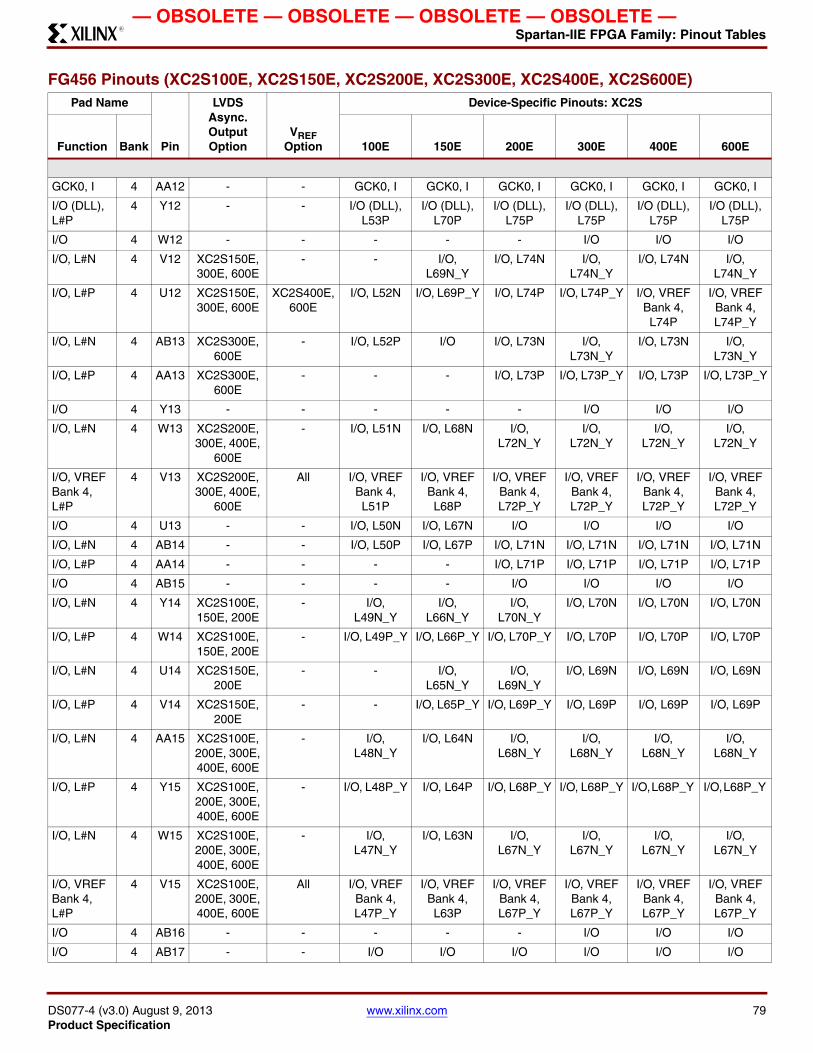
Spartan-IIE FPGA Family: Pinout TablesR
— OBSOLETE — OBSOLETE — OBSOLETE — OBSOLETE —
GCK0, I 4 AA12 - - GCK0, I GCK0, I GCK0, I GCK0, I GCK0, I GCK0, I
I/O (DLL), L#P
4 Y12 - - I/O (DLL), L53P
I/O (DLL), L70P
I/O (DLL), L75P
I/O (DLL), L75P
I/O (DLL), L75P
I/O (DLL), L75P
I/O 4 W12 - - - - - I/O I/O I/O
I/O, L#N 4 V12 XC2S150E, 300E, 600E
- - I/O, L69N_Y
I/O, L74N I/O, L74N_Y
I/O, L74N I/O, L74N_Y
I/O, L#P 4 U12 XC2S150E, 300E, 600E
XC2S400E, 600E
I/O, L52N I/O, L69P_Y I/O, L74P I/O, L74P_Y I/O, VREF Bank 4, L74P
I/O, VREF Bank 4, L74P_Y
I/O, L#N 4 AB13 XC2S300E, 600E
- I/O, L52P I/O I/O, L73N I/O, L73N_Y
I/O, L73N I/O, L73N_Y
I/O, L#P 4 AA13 XC2S300E, 600E
- - - I/O, L73P I/O, L73P_Y I/O, L73P I/O, L73P_Y
I/O 4 Y13 - - - - - I/O I/O I/O
I/O, L#N 4 W13 XC2S200E, 300E, 400E,
600E
- I/O, L51N I/O, L68N I/O, L72N_Y
I/O, L72N_Y
I/O, L72N_Y
I/O, L72N_Y
I/O, VREF Bank 4, L#P
4 V13 XC2S200E, 300E, 400E,
600E
All I/O, VREF Bank 4, L51P
I/O, VREF Bank 4, L68P
I/O, VREF Bank 4, L72P_Y
I/O, VREF Bank 4, L72P_Y
I/O, VREF Bank 4, L72P_Y
I/O, VREF Bank 4, L72P_Y
I/O 4 U13 - - I/O, L50N I/O, L67N I/O I/O I/O I/O
I/O, L#N 4 AB14 - - I/O, L50P I/O, L67P I/O, L71N I/O, L71N I/O, L71N I/O, L71N
I/O, L#P 4 AA14 - - - - I/O, L71P I/O, L71P I/O, L71P I/O, L71P
I/O 4 AB15 - - - - I/O I/O I/O I/O
I/O, L#N 4 Y14 XC2S100E, 150E, 200E
- I/O, L49N_Y
I/O, L66N_Y
I/O, L70N_Y
I/O, L70N I/O, L70N I/O, L70N
I/O, L#P 4 W14 XC2S100E, 150E, 200E
- I/O, L49P_Y I/O, L66P_Y I/O, L70P_Y I/O, L70P I/O, L70P I/O, L70P
I/O, L#N 4 U14 XC2S150E, 200E
- - I/O, L65N_Y
I/O, L69N_Y
I/O, L69N I/O, L69N I/O, L69N
I/O, L#P 4 V14 XC2S150E, 200E
- - I/O, L65P_Y I/O, L69P_Y I/O, L69P I/O, L69P I/O, L69P
I/O, L#N 4 AA15 XC2S100E, 200E, 300E, 400E, 600E
- I/O, L48N_Y
I/O, L64N I/O, L68N_Y
I/O, L68N_Y
I/O, L68N_Y
I/O, L68N_Y
I/O, L#P 4 Y15 XC2S100E, 200E, 300E, 400E, 600E
- I/O, L48P_Y I/O, L64P I/O, L68P_Y I/O, L68P_Y I/O, L68P_Y I/O, L68P_Y
I/O, L#N 4 W15 XC2S100E, 200E, 300E, 400E, 600E
- I/O, L47N_Y
I/O, L63N I/O, L67N_Y
I/O, L67N_Y
I/O, L67N_Y
I/O, L67N_Y
I/O, VREF Bank 4, L#P
4 V15 XC2S100E, 200E, 300E, 400E, 600E
All I/O, VREF Bank 4, L47P_Y
I/O, VREF Bank 4, L63P
I/O, VREF Bank 4, L67P_Y
I/O, VREF Bank 4, L67P_Y
I/O, VREF Bank 4, L67P_Y
I/O, VREF Bank 4, L67P_Y
I/O 4 AB16 - - - - - I/O I/O I/O
I/O 4 AB17 - - I/O I/O I/O I/O I/O I/O
FG456 Pinouts (XC2S100E, XC2S150E, XC2S200E, XC2S300E, XC2S400E, XC2S600E) Pad Name
Pin
LVDS Async. Output Option
VREF Option
Device-Specific Pinouts: XC2S
Function Bank 100E 150E 200E 300E 400E 600E
DS077-4 (v3.0) August 9, 2013 www.xilinx.com 79Product Specification

Spartan-IIE FPGA Family: Pinout TablesR
— OBSOLETE — OBSOLETE — OBSOLETE — OBSOLETE —
I/O, L#N 4 AA16 XC2S150E, 200E, 400E
XC2S600E I/O, L46N I/O, L62N_Y
I/O, L66N_Y
I/O, L66N I/O, L66N_Y
I/O, VREF Bank 4, L66N
I/O, L#P 4 Y16 XC2S150E, 200E, 400E
- I/O, L46P I/O, L62P_Y I/O, L66P_Y I/O, L66P I/O, L66P_Y I/O, L66P
I/O, L#N 4 W16 XC2S150E, 200E
- - I/O, L61N_Y
I/O, L65N_Y
I/O, L65N I/O, L65N I/O, L65N
I/O, L#P 4 V16 XC2S150E, 200E
- - I/O, L61P_Y I/O, L65P_Y I/O, L65P I/O, L65P I/O, L65P
I/O, L#N_YY
4 AA17 All - I/O, L45N_YY
I/O, L60N_YY
I/O, L64N_YY
I/O, L64N_YY
I/O, L64N_YY
I/O, L64N_YY
I/O, VREF Bank 4, L#P_YY
4 Y17 All All I/O, VREF Bank 4,
L45P_YY
I/O, VREF Bank 4,
L60P_YY
I/O, VREF Bank 4,
L64P_YY
I/O, VREF Bank 4,
L64P_YY
I/O, VREF Bank 4,
L64P_YY
I/O, VREF Bank 4,
L64P_YY
I/O 4 AB18 XC2S100E - I/O, L44N_Y
I/O I/O I/O I/O I/O
I/O, L#N 4 W17 XC2S100E, 400E, 600E
- I/O, L44P_Y I/O, L59N I/O, L63N I/O, L63N I/O, L63N_Y
I/O, L63N_Y
I/O, L#P 4 V17 XC2S400E, 600E
- - I/O, L59P I/O, L63P I/O, L63P I/O, L63P_Y I/O, L63P_Y
I/O 4 AA18 - - - - - I/O I/O I/O
I/O, L#N 4 Y18 XC2S100E, 200E, 300E, 400E, 600E
- I/O, L43N_Y
I/O, L58N I/O, L62N_Y
I/O, L62N_Y
I/O, L62N_Y
I/O, L62N_Y
I/O, L#P 4 W18 XC2S100E, 200E, 300E, 400E, 600E
XC2S200E, 300E,
400E, 600E
I/O, L43P_Y I/O, L58P I/O, VREF Bank 4, L62P_Y
I/O, VREF Bank 4, L62P_Y
I/O, VREF Bank 4, L62P_Y
I/O, VREF Bank 4, L62P_Y
I/O 4 AB19 - - I/O I/O I/O I/O I/O I/O
I/O, L#N 4 AA19 XC2S150E, 400E
- - I/O, L57N_Y
I/O, L61N I/O, L61N I/O, L61N_Y
I/O, L61N
I/O, L#P 4 Y19 XC2S150E, 400E
- - I/O, L57P_Y I/O, L61P I/O, L61P I/O, L61P_Y I/O, L61P
I/O 4 AB21 - - - - - I/O I/O I/O
I/O, L#N_YY
4 AB20 All - I/O, L42N_YY
I/O, L56N_YY
I/O, L60N_YY
I/O, L60N_YY
I/O, L60N_YY
I/O, L60N_YY
I/O, L#P_YY
4 AA20 All - I/O, L42P_YY
I/O, L56P_YY
I/O, L60P_YY
I/O, L60P_YY
I/O, L60P_YY
I/O, L60P_YY
DONE 3 W20 - - DONE DONE DONE DONE DONE DONE
PROGRAM - Y21 - - PROGRAM PROGRAM PROGRAM PROGRAM PROGRAM PROGRAM
I/O (INIT), L#N_YY
3 W21 All - I/O (INIT), L41N_YY
I/O (INIT), L55N_YY
I/O (INIT), L59N_YY
I/O (INIT), L59N_YY
I/O (INIT), L59N_YY
I/O (INIT), L59N_YY
I/O (D7), L#P_YY
3 Y22 All - I/O (D7), L41P_YY
I/O (D7), L55P_YY
I/O (D7), L59P_YY
I/O (D7), L59P_YY
I/O (D7), L59P_YY
I/O (D7), L59P_YY
I/O 3 W22 - - - - - I/O I/O I/O
I/O 3 V21 - - - I/O I/O I/O I/O I/O
FG456 Pinouts (XC2S100E, XC2S150E, XC2S200E, XC2S300E, XC2S400E, XC2S600E) Pad Name
Pin
LVDS Async. Output Option
VREF Option
Device-Specific Pinouts: XC2S
Function Bank 100E 150E 200E 300E 400E 600E
80 www.xilinx.com DS077-4 (v3.0) August 9, 2013Product Specification

Spartan-IIE FPGA Family: Pinout TablesR
— OBSOLETE — OBSOLETE — OBSOLETE — OBSOLETE —
I/O, L#N 3 V19 XC2S150E, 200E, 300E,
400E
- - I/O, L54N_Y
I/O, L58N_Y
I/O, L58N_Y
I/O, L58N_Y
I/O, L58N
I/O, L#P 3 V20 XC2S150E, 200E, 300E,
400E
- I/O I/O, L54P_Y I/O, L58P_Y I/O, L58P_Y I/O, L58P_Y I/O, L58P
I/O, L#N 3 V22 XC2S100E, 200E, 300E,
600E
XC2S200E, 300E,
400E, 600E
I/O, L40N_Y
I/O, L53N I/O, VREF Bank 3, L57N_Y
I/O, VREF Bank 3, L57N_Y
I/O, VREF Bank 3, L57N
I/O, VREF Bank 3, L57N_Y
I/O, L#P 3 U22 XC2S100E, 200E, 300E,
600E
- I/O, L40P_Y I/O, L53P I/O, L57P_Y I/O, L57P_Y I/O, L57P I/O, L57P_Y
I/O 3 U21 - - - - - I/O I/O I/O
I/O 3 U20 - - - I/O I/O I/O I/O I/O
I/O, L#N 3 U18 XC2S100E, 200E, 300E,
600E
- I/O, L39N_Y
I/O, L52N I/O, L56N_Y
I/O, L56N_Y
I/O, L56N I/O, L56N_Y
I/O, L#P 3 U19 XC2S100E, 200E, 300E,
600E
- I/O, L39P_Y I/O, L52P I/O, L56P_Y I/O, L56P_Y I/O, L56P I/O, L56P_Y
I/O, VREF Bank 3, L#N
3 T21 XC2S150E, 200E, 300E, 400E, 600E
All I/O, VREF Bank 3, L38N
I/O, VREF Bank 3, L51N_Y
I/O, VREF Bank 3, L55N_Y
I/O, VREF Bank 3, L55N_Y
I/O, VREF Bank 3, L55N_Y
I/O, VREF Bank 3, L55N_Y
I/O, L#P 3 T22 XC2S150E, 200E, 300E, 400E, 600E
- I/O, L38P I/O, L51P_Y I/O, L55P_Y I/O, L55P_Y I/O, L55P_Y I/O, L55P_Y
I/O 3 T20 - - - I/O I/O I/O I/O I/O
I/O, L#N 3 T18 XC2S150E, 200E, 300E,
400E
- - I/O, L50N_Y
I/O, L54N_Y
I/O, L54N_Y
I/O, L54N_Y
I/O, L54N
I/O, L#P 3 T19 XC2S150E, 200E, 300E,
400E
- I/O I/O, L50P_Y I/O, L54P_Y I/O, L54P_Y I/O, L54P_Y I/O, L54P
I/O, L#N 3 R21 XC2S100E, 150E, 300E,
600E
XC2S600E I/O, L37N_Y
I/O, L49N_Y
I/O, L53N I/O, L53N_Y
I/O, L53N I/O, VREF Bank 3, L53N_Y
I/O, L#P 3 R22 XC2S100E, 150E, 300E,
600E
- I/O, L37P_Y I/O, L49P_Y I/O, L53P I/O, L53P_Y I/O, L53P I/O, L53P_Y
I/O 3 R20 - - - - - I/O I/O I/O
I/O, VREF Bank 3, L#N
3 R18 XC2S300E, 400E, 600E
All I/O, VREF Bank 3, L36N
I/O, VREF Bank 3, L48N
I/O, VREF Bank 3, L52N
I/O, VREF Bank 3, L52N_Y
I/O, VREF Bank 3, L52N_Y
I/O, VREF Bank 3, L52N_Y
I/O (D6), L#P
3 R19 XC2S300E, 400E, 600E
- I/O (D6), L36P
I/O (D6), L48P
I/O (D6), L52P
I/O (D6), L52P_Y
I/O (D6), L52P_Y
I/O (D6), L52P_Y
I/O (D5), L#N_YY
3 P22 All - I/O (D5), L35N_YY
I/O (D5), L47N_YY
I/O (D5), L51N_YY
I/O (D5), L51N_YY
I/O (D5) L51N_YY
I/O (D5), L51N_YY
I/O, L#P_YY
3 P21 All - I/O, L35P_YY
I/O, L47P_YY
I/O, L51P_YY
I/O, L51P_YY
I/O, L51P_YY
I/O, L51P_YY
FG456 Pinouts (XC2S100E, XC2S150E, XC2S200E, XC2S300E, XC2S400E, XC2S600E) Pad Name
Pin
LVDS Async. Output Option
VREF Option
Device-Specific Pinouts: XC2S
Function Bank 100E 150E 200E 300E 400E 600E
DS077-4 (v3.0) August 9, 2013 www.xilinx.com 81Product Specification

Spartan-IIE FPGA Family: Pinout TablesR
— OBSOLETE — OBSOLETE — OBSOLETE — OBSOLETE —
I/O 3 P20 - - - - I/O I/O I/O I/O
I/O, L#N 3 P18 XC2S150E, 200E, 300E,
400E
- - I/O, L46N_Y
I/O, L50N_Y
I/O, L50N_Y
I/O, L50N_Y
I/O, L50N
I/O, L#P 3 P19 XC2S100E, 150E, 200E, 300E, 400E
- I/O, L34N_Y
I/O, L46P_Y I/O, L50P_Y I/O, L50P_Y I/O, L50P_Y I/O, L50P
I/O, L#N 3 N22 XC2S100E, 150E, 200E, 300E, 600E
- I/O, L34P_Y I/O, L45N_Y
I/O, L49N_Y
I/O, L49N_Y
I/O, L49N I/O, L49N_Y
I/O, L#P 3 N21 XC2S150E, 200E, 300E,
600E
- - I/O, L45P_Y I/O, L49P_Y I/O, L49P_Y I/O, L49P I/O, L49P_Y
I/O 3 P17 - - - - I/O I/O I/O I/O
I/O, L#N 3 N19 XC2S100E, 150E, 200E,
300E, 600E(1)
- I/O, L33N_YY
I/O, L44N_YY
I/O, L48N_YY
I/O, L48N_YY
I/O, L48N I/O, L48N_Y
I/O, L#P 3 N20 XC2S100E, 150E, 200E,
300E, 600E(1)
- I/O, L33P_YY
I/O, L44P_YY
I/O, L48P_YY
I/O, L48P_YY
I/O, L48P I/O, L48P_Y
I/O, VREF Bank 3, L#N
3 N18 XC2S300E, 400E, 600E
All I/O, VREF Bank 3, L32N
I/O, VREF Bank 3, L43N
I/O, VREF Bank 3, L47N
I/O, VREF Bank 3, L47N_Y
I/O, VREF Bank 3, L47N_Y
I/O, VREF Bank 3, L47N_Y
I/O (D4), L#P
3 N17 XC2S300E, 400E, 600E
- I/O (D4), L32P
I/O (D4), L43P
I/O (D4), L47P
I/O (D4), L47P_Y
I/O (D4), L47P_Y
I/O (D4), L47P_Y
I/O 3 M22 - - - - - I/O I/O I/O
I/O, L#N 3 M20 XC2S300E, 400E
- - - I/O, L46N I/O, L46N_Y
I/O, L46N_Y
I/O, L46N
I/O, L#P 3 M21 XC2S100E, 150E, 300E,
400E
- I/O, L31N_Y
I/O, L42N_Y
I/O, L46P I/O, L46P_Y I/O, L46P_Y I/O, L46P
I/O, L#N 3 M18 XC2S100E, 150E, 200E, 300E, 600E
XC2S400E, 600E
I/O, L31P_Y I/O, L42P_Y I/O, L45N_Y
I/O, L45N_Y
I/O, VREF Bank 3, L45N
I/O, VREF Bank 3, L45N_Y
I/O, L#P 3 M19 XC2S200E, 300E, 600E
- - I/O I/O, L45P_Y I/O, L45P_Y I/O, L45P I/O, L45P_Y
I/O 3 M17 - - - - - I/O I/O I/O
I/O (TRDY) 3 L22 - - I/O (TRDY) I/O (TRDY) I/O (TRDY) I/O (TRDY) I/O (TRDY) I/O (TRDY)
I/O (IRDY), L#N_YY
2 L21 All - I/O (IRDY), L30N_YY
I/O (IRDY), L41N_YY
I/O (IRDY), L44N_YY
I/O (IRDY), L44N_YY
I/O (IRDY), L44N_YY
I/O (IRDY), L44N_YY
I/O, L#P_YY
2 L20 All - I/O, L30P_YY
I/O, L41P_YY
I/O, L44P_YY
I/O, L44P_YY
I/O, L44P_YY
I/O, L44P_YY
I/O 2 L19 - - - - - I/O I/O I/O
I/O, L#N 2 L18 XC2S200E, 300E, 600E
- - I/O I/O, L43N_Y
I/O, L43N_Y
I/O, L43N I/O, L43N_Y
FG456 Pinouts (XC2S100E, XC2S150E, XC2S200E, XC2S300E, XC2S400E, XC2S600E) Pad Name
Pin
LVDS Async. Output Option
VREF Option
Device-Specific Pinouts: XC2S
Function Bank 100E 150E 200E 300E 400E 600E
82 www.xilinx.com DS077-4 (v3.0) August 9, 2013Product Specification
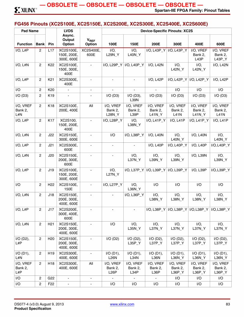
Spartan-IIE FPGA Family: Pinout TablesR
— OBSOLETE — OBSOLETE — OBSOLETE — OBSOLETE —
I/O, L#P 2 L17 XC2S100E, 150E, 200E, 300E, 600E
XC2S400E, 600E
I/O, L29N_Y
I/O, L40N_Y
I/O, L43P_Y I/O, L43P_Y I/O, VREF Bank 2, L43P
I/O, VREF Bank 2, L43P_Y
I/O, L#N 2 K22 XC2S100E, 150E, 300E,
400E
- I/O, L29P_Y I/O, L40P_Y I/O, L42N I/O, L42N_Y
I/O, L42N_Y
I/O, L42N
I/O, L#P 2 K21 XC2S300E, 400E
- - - I/O, L42P I/O, L42P_Y I/O, L42P_Y I/O, L42P
I/O 2 K20 - - - - - I/O I/O I/O
I/O (D3) 2 K19 - - I/O (D3) I/O (D3), L39N
I/O (D3) I/O (D3) I/O (D3) I/O (D3)
I/O, VREF Bank 2, L#N
2 K18 XC2S100E, 200E, 400E
All I/O, VREF Bank 2, L28N_Y
I/O, VREF Bank 2, L39P
I/O, VREF Bank 2, L41N_Y
I/O, VREF Bank 2, L41N
I/O, VREF Bank 2, L41N_Y
I/O, VREF Bank 2, L41N
I/O, L#P 2 K17 XC2S100, 150E, 200E,
400E
- I/O, L28P_Y I/O, L38N_Y
I/O, L41P_Y I/O, L41P I/O, L41P_Y I/O, L41P
I/O, L#N 2 J22 XC2S150E, 300E, 600E
- I/O I/O, L38P_Y I/O, L40N I/O, L40N_Y
I/O, L40N I/O, L40N_Y
I/O, L#P 2 J21 XC2S300E, 600E
- - - I/O, L40P I/O, L40P_Y I/O, L40P I/O, L40P_Y
I/O, L#N 2 J20 XC2S150E, 200E, 300E,
600E
- - I/O, L37N_Y
I/O, L39N_Y
I/O, L39N_Y
I/O, L39N I/O, L39N_Y
I/O, L#P 2 J19 XC2S100E, 150E, 200E, 300E, 600E
- I/O, L27N_Y
I/O, L37P_Y I/O, L39P_Y I/O, L39P_Y I/O, L39P I/O, L39P_Y
I/O 2 H22 XC2S100E, 150E
- I/O, L27P_Y I/O, L36N_Y
I/O I/O I/O I/O
I/O, L#N 2 J18 XC2S150E, 200E, 300E, 400E, 600E
- - I/O, L36P_Y I/O, L38N_Y
I/O, L38N_Y
I/O, L38N_Y
I/O, L38N_Y
I/O, L#P 2 J17 XC2S200E, 300E, 400E,
600E
- - - I/O, L38P_Y I/O, L38P_Y I/O, L38P_Y I/O, L38P_Y
I/O, L#N 2 H21 XC2S150E, 200E, 300E, 400E, 600E
- I/O I/O, L35N_Y
I/O, L37N_Y
I/O, L37N_Y
I/O, L37N_Y
I/O, L37N_Y
I/O (D2), L#P
2 H20 XC2S150E, 200E, 300E, 400E, 600E
- I/O (D2) I/O (D2), L35P_Y
I/O (D2), L37P_Y
I/O (D2), L37P_Y
I/O (D2), L37P_Y
I/O (D2), L37P_Y
I/O (D1), L#N
2 H19 XC2S300E, 400E, 600E
- I/O (D1), L26N
I/O (D1), L34N
I/O (D1), L36N
I/O (D1), L36N_Y
I/O (D1), L36N_Y
I/O (D1), L36N_Y
I/O, VREF Bank 2, L#P
2 H18 XC2S300E, 400E, 600E
All I/O, VREF Bank 2, L26P
I/O, VREF Bank 2, L34P
I/O, VREF Bank 2, L36P
I/O, VREF Bank 2, L36P_Y
I/O, VREF Bank 2, L36P_Y
I/O, VREF Bank 2, L36P_Y
I/O 2 G22 - - - - - I/O I/O I/O
I/O 2 F22 - - I/O I/O I/O I/O I/O I/O
FG456 Pinouts (XC2S100E, XC2S150E, XC2S200E, XC2S300E, XC2S400E, XC2S600E) Pad Name
Pin
LVDS Async. Output Option
VREF Option
Device-Specific Pinouts: XC2S
Function Bank 100E 150E 200E 300E 400E 600E
DS077-4 (v3.0) August 9, 2013 www.xilinx.com 83Product Specification

Spartan-IIE FPGA Family: Pinout TablesR
— OBSOLETE — OBSOLETE — OBSOLETE — OBSOLETE —
I/O, L#N 2 G21 XC2S200E, 400E, 600E
XC2S600E I/O, L25N I/O, L33N I/O, L35N_Y
I/O, L35N I/O, L35N_Y
I/O, VREF Bank 2, L35N_Y
I/O, L#P 2 G20 XC2S200E, 400E, 600E
- I/O, L25P I/O, L33P I/O, L35P_Y I/O, L35P I/O, L35P_Y I/O, L35P_Y
I/O, L#N 2 G19 XC2S150E, 300E
- - I/O, L32N_Y
I/O, L34N I/O, L34N_Y
I/O, L34N I/O, L34N
I/O, L#P 2 G18 XC2S150E, 300E
- - I/O, L32P_Y I/O, L34P I/O, L34P_Y I/O, L34P I/O, L34P
I/O, L#N 2 E22 XC2S150E, 200E, 300E, 400E, 600E
- I/O, L24N I/O, L31N_Y
I/O, L33N_Y
I/O, L33N_Y
I/O, L33N_Y
I/O, L33N_Y
I/O, VREF Bank 2, L#P
2 F21 XC2S150E, 200E, 300E, 400E, 600E
All I/O, VREF Bank 2, L24P
I/O, VREF Bank 2, L31P_Y
I/O, VREF Bank 2, L33P_Y
I/O, VREF Bank 2, L33P_Y
I/O, VREF Bank 2, L33P_Y
I/O, VREF Bank 2, L33P_Y
I/O 2 E21 XC2S100E - I/O, L23N_Y
I/O I/O I/O I/O I/O
I/O, L#N 2 F20 XC2S100E, 150E, 200E, 300E, 400E,
600E
- I/O, L23P_Y I/O, L30N_Y
I/O, L32N_Y
I/O, L32N_Y
I/O, L32N_Y
I/O, L32N_Y
I/O, L#P 2 F19 XC2S150E, 200E, 300E, 400E, 600E
- - I/O, L30P_Y I/O, L32P_Y I/O, L32P_Y I/O, L32P_Y I/O, L32P_Y
I/O 2 F18 - - - - - I/O I/O I/O
I/O, L#N 2 D22 XC2S100E, 200E, 300E,
600E
- I/O, L22N_Y
I/O, L29N I/O, L31N_Y
I/O, L31N_Y
I/O, L31N I/O, L31N_Y
I/O, L#P 2 D21 XC2S100E, 200E, 300E,
600E
XC2S200E, 300E,
400E, 600E
I/O, L22P_Y I/O, L29P I/O, VREF Bank 2, L31P_Y
I/O, VREF Bank 2, L31P_Y
I/O, VREF Bank 2, L31P
I/O, VREF Bank 2, L31P_Y
I/O, L#N 2 E20 XC2S200E, 300E, 400E
- I/O I/O, L28N I/O, L30N_Y
I/O, L30N_Y
I/O, L30N_Y
I/O, L30N
I/O, L#P 2 E19 XC2S200E, 300E, 400E
- - I/O, L28P I/O, L30P_Y I/O, L30P_Y I/O, L30P_Y I/O, L30P
I/O 2 D20 - - - - - I/O I/O I/O
I/O (DIN, D0), L#N_YY
2 C22 All - I/O (DIN, D0),
L21N_YY
I/O (DIN, D0),
L27N_YY
I/O (DIN, D0),
L29N_YY
I/O (DIN, D0),
L29N_YY
I/O (DIN, D0),
L29N_YY
I/O (DIN, D0),
L29N_YY
I/O (DOUT, BUSY), L#P_YY
2 C21 All - I/O (DOUT, BUSY),
L21P_YY
I/O (DOUT, BUSY),
L27P_YY
I/O (DOUT, BUSY),
L29P_YY
I/O (DOUT, BUSY),
L29P_YY
I/O (DOUT, BUSY),
L29P_YY
I/O (DOUT, BUSY),
L29P_YY
CCLK 2 B22 - - CCLK CCLK CCLK CCLK CCLK CCLK
TDO 2 A21 - - TDO TDO TDO TDO TDO TDO
TDI - C19 - - TDI TDI TDI TDI TDI TDI
I/O (CS), L#P_YY
1 B20 All - I/O (CS), L20P_YY
I/O (CS), L26P_YY
I/O (CS), L28P_YY
I/O (CS), L28P_YY
I/O (CS), L28P_YY
I/O (CS), L28P_YY
FG456 Pinouts (XC2S100E, XC2S150E, XC2S200E, XC2S300E, XC2S400E, XC2S600E) Pad Name
Pin
LVDS Async. Output Option
VREF Option
Device-Specific Pinouts: XC2S
Function Bank 100E 150E 200E 300E 400E 600E
84 www.xilinx.com DS077-4 (v3.0) August 9, 2013Product Specification

Spartan-IIE FPGA Family: Pinout TablesR
— OBSOLETE — OBSOLETE — OBSOLETE — OBSOLETE —
I/O (WRITE), L#N_YY
1 A20 All - I/O (WRITE), L20N_YY
I/O (WRITE), L26N_YY
I/O (WRITE), L28N_YY
I/O (WRITE), L28N_YY
I/O (WRITE), L28N_YY
I/O (WRITE), L28N_YY
I/O 1 D18 - - - - - I/O I/O I/O
I/O 1 C18 - - - I/O I/O I/O I/O I/O
I/O, L#P 1 B19 XC2S200E, 300E, 400E,
600E
- - I/O, L25P I/O, L27P_Y I/O, L27P_Y I/O, L27P_Y I/O, L27P_Y
I/O, L#N 1 A19 XC2S200E, 300E, 400E,
600E
- I/O I/O, L25N I/O, L27N_Y
I/O, L27N_Y
I/O, L27N_Y
I/O, L27N_Y
I/O, L#P 1 B18 XC2S100E, 200E, 300E, 400E, 600E
XC2S200E, 300E,
400E, 600E
I/O, L19P_Y I/O, L24P I/O, VREF Bank 1, L26P_Y
I/O, VREF Bank 1, L26P_Y
I/O, VREF Bank 1, L26P_Y
I/O, VREF Bank 1, L26P_Y
I/O, L#N 1 A18 XC2S100E, 200E, 300E, 400E, 600E
- I/O, L19N_Y
I/O, L24N I/O, L26N_Y
I/O, L26N_Y
I/O, L26N_Y
I/O, L26N_Y
I/O 1 D17 - - - - - I/O I/O I/O
I/O 1 C17 - - - I/O I/O I/O I/O I/O
I/O, L#P_YY
1 B17 All - I/O, L18P_YY
I/O, L23P_YY
I/O, L25P_YY
I/O, L25P_YY
I/O, L25P_YY
I/O, L25P_YY
I/O, L#N_YY
1 A17 All - I/O, L18N_YY
I/O, L23N_YY
I/O, L25N_YY
I/O, L25N_YY
I/O, L25N_YY
I/O, L25N_YY
I/O, VREF Bank 1, L#P_YY
1 E16 All All I/O, VREF Bank 1,
L17P_YY
I/O, VREF Bank 1,
L22P_YY
I/O, VREF Bank 1,
L24P_YY
I/O, VREF Bank 1,
L24P_YY
I/O, VREF Bank 1,
L24P_YY
I/O, VREF Bank 1,
L24P_YY
I/O, L#N_YY
1 E17 All - I/O, L17N_YY
I/O, L22N_YY
I/O, L24N_YY
I/O, L24N_YY
I/O, L24N_YY
I/O, L24N_YY
I/O 1 E15 - - - I/O I/O I/O I/O I/O
I/O, L#P 1 D16 XC2S300E, 600E
- - I/O, L21P I/O, L23P I/O, L23P_Y I/O, L23P I/O, L23P_Y
I/O, L#N 1 C16 XC2S300E, 600E
- I/O I/O, L21N I/O, L23N I/O, L23N_Y
I/O, L23N I/O, L23N_Y
I/O, L#P 1 B16 XC2S100E, 300E, 600E
XC2S600E I/O, L16P_Y I/O, L20P I/O, L22P I/O, L22P_Y I/O, L22P I/O, VREF Bank 1, L22P_Y
I/O, L#N 1 A16 XC2S100E, 300E, 600E
- I/O, L16N_Y
I/O, L20N I/O, L22N I/O, L22N_Y
I/O, L22N I/O, L22N_Y
I/O 1 F14 - - - - - I/O I/O I/O
I/O, VREF Bank 1, L#P
1 D15 XC2S100E, 200E, 300E, 400E, 600E
All I/O, VREF Bank 1, L15P_Y
I/O, VREF Bank 1, L19P
I/O, VREF Bank 1, L21P_Y
I/O, VREF Bank 1, L21P_Y
I/O, VREF Bank 1, L21P_Y
I/O, VREF Bank 1, L21P_Y
I/O, L#N 1 C15 XC2S100E, 200E, 300E, 400E, 600E
- I/O, L15N_Y
I/O, L19N I/O, L21N_Y
I/O, L21N_Y
I/O, L21N_Y
I/O, L21N_Y
I/O, L#P 1 B15 XC2S100E, 200E, 300E, 400E, 600E
- I/O, L14P_Y I/O, L18P I/O, L20P_Y I/O, L20P_Y I/O, L20P_Y I/O, L20P_Y
FG456 Pinouts (XC2S100E, XC2S150E, XC2S200E, XC2S300E, XC2S400E, XC2S600E) Pad Name
Pin
LVDS Async. Output Option
VREF Option
Device-Specific Pinouts: XC2S
Function Bank 100E 150E 200E 300E 400E 600E
DS077-4 (v3.0) August 9, 2013 www.xilinx.com 85Product Specification

Spartan-IIE FPGA Family: Pinout TablesR
— OBSOLETE — OBSOLETE — OBSOLETE — OBSOLETE —
I/O, L#N 1 A15 XC2S100E, 200E, 300E, 400E, 600E
- I/O, L14N_Y
I/O, L18N I/O, L20N_Y
I/O, L20N_Y
I/O, L20N_Y
I/O, L20N_Y
I/O 1 E14 - - - - I/O I/O I/O I/O
I/O, L#P 1 D14 XC2S150E, 300E, 400E,
600E
- - I/O, L17P_Y I/O, L19P I/O, L19P_Y I/O, L19P_Y I/O, L19P_Y
I/O, L#N 1 C14 XC2S100E, 150E, 300E, 400E, 600E
- I/O, L13P_Y I/O, L17N_Y
I/O, L19N I/O, L19N_Y
I/O, L19N_Y
I/O, L19N_Y
I/O, L#P 1 B14 XC2S100E, 150E, 300E, 400E, 600E
- I/O, L13N_Y
I/O, L16P_Y I/O, L18P I/O, L18P_Y I/O, L18P_Y I/O, L18P_Y
I/O, L#N 1 A14 XC2S150E, 300E, 400E,
600E
- - I/O, L16N_Y
I/O, L18N I/O, L18N_Y
I/O, L18N_Y
I/O, L18N_Y
I/O 1 E13 - - - - I/O I/O I/O I/O
I/O, L#P 1 D13 XC2S200E, 300E, 400E,
600E
- I/O, L12P I/O, L15P I/O, L17P_Y I/O, L17P_Y I/O, L17P_Y I/O, L17P_Y
I/O, L#N 1 C13 XC2S200E, 300E, 400E,
600E
- I/O, L12N I/O, L15N I/O, L17N_Y
I/O, L17N_Y
I/O, L17N_Y
I/O, L17N_Y
I/O, VREF Bank 1, L#P
1 B13 XC2S200E, 300E, 400E,
600E
All I/O, VREF Bank 1, L11P
I/O, VREF Bank 1, L14P
I/O, VREF Bank 1, L16P_Y
I/O, VREF Bank 1, L16P_Y
I/O, VREF Bank 1, L16P_Y
I/O, VREF Bank 1, L16P_Y
I/O, L#N 1 A13 XC2S200E, 300E, 400E,
600E
- I/O, L11N I/O, L14N I/O, L16N_Y
I/O, L16N_Y
I/O, L16N_Y
I/O, L16N_Y
I/O 1 F13 - - - - - I/O I/O I/O
I/O, L#P 1 C12 XC2S300E, 600E
- - - I/O, L15P I/O, L15P_Y I/O, L15P I/O, L15P_Y
I/O, L#N 1 B12 XC2S300E, 600E
- I/O, L10P I/O I/O, L15N I/O, L15N_Y
I/O, L15N I/O, L15N_Y
I/O, L#P 1 D12 XC2S150E, 300E, 600E
XC2S400E, 600E
I/O, L10N I/O, L13P_Y I/O, L14P I/O, L14P_Y I/O, VREF Bank 1, L14P
I/O, VREF Bank 1, L14P_Y
I/O, L#N 1 E12 XC2S150E, 300E, 600E
- - I/O, L13N_Y
I/O, L14N I/O, L14N_Y
I/O, L14N I/O, L14N_Y
I/O 1 F12 - - - - - I/O I/O I/O
I/O (DLL), L#P
1 A12 - - I/O (DLL), L9P
I/O (DLL), L12P
I/O (DLL), L13P
I/O (DLL), L13P
I/O (DLL), L13P
I/O (DLL), L13P
GCK2, I 1 A11 - - GCK2, I GCK2, I GCK2, I GCK2, I GCK2, I GCK2, I
GCK3, I 0 C11 - - GCK3, I GCK3, I GCK3, I GCK3, I GCK3, I GCK3, I
I/O (DLL), L#N
0 B11 - - I/O (DLL), L9N
I/O (DLL), L12N
I/O (DLL), L13N
I/O (DLL), L13N
I/O (DLL), L13N
I/O (DLL), L13N
I/O 0 D11 - - - - - I/O I/O I/O
FG456 Pinouts (XC2S100E, XC2S150E, XC2S200E, XC2S300E, XC2S400E, XC2S600E) Pad Name
Pin
LVDS Async. Output Option
VREF Option
Device-Specific Pinouts: XC2S
Function Bank 100E 150E 200E 300E 400E 600E
86 www.xilinx.com DS077-4 (v3.0) August 9, 2013Product Specification

Spartan-IIE FPGA Family: Pinout TablesR
— OBSOLETE — OBSOLETE — OBSOLETE — OBSOLETE —
I/O 0 F11 - XC2S400E, 600E
- - I/O I/O I/O, VREF Bank 0
I/O, VREF Bank 0
I/O, L#P 0 A10 XC2S300E, 600E
- I/O I/O, L11P I/O, L12P I/O, L12P_Y I/O, L12P I/O, L12P_Y
I/O, L#N 0 B10 XC2S300E, 600E
- - I/O, L11N I/O, L12N I/O, L12N_Y
I/O, L12N I/O, L12N_Y
I/O 0 E11 - - - - - I/O I/O I/O
I/O, L#P 0 C10 XC2S200E, 300E, 400E,
600E
- I/O, L8P I/O, L10P I/O, L11P_Y I/O, L11P_Y I/O, L11P_Y I/O, L11P_Y
I/O, VREF Bank 0, L#N
0 D10 XC2S200E, 300E, 400E,
600E
All I/O, VREF Bank 0,
L8N
I/O, VREF Bank 0, L10N
I/O, VREF Bank 0, L11N_Y
I/O, VREF Bank 0, L11N_Y
I/O, VREF Bank 0, L11N_Y
I/O, VREF Bank 0, L11N_Y
I/O 0 F10 - - I/O, L7P I/O I/O I/O I/O I/O
I/O, L#P 0 A9 - - I/O, L7N I/O I/O, L10P I/O, L10P I/O, L10P I/O, L10P
I/O, L#N 0 B9 - - - - I/O, L10N I/O, L10N I/O, L10N I/O, L10N
I/O 0 E10 - - - - I/O I/O I/O I/O
I/O, L#P 0 C9 XC2S100E, 150E, 200E
- I/O, L6P_Y I/O, L9P_Y I/O, L9P_Y I/O, L9P I/O, L9P I/O, L9P
I/O, L#N 0 D9 XC2S100E, 150E, 200E
- I/O, L6N_Y I/O, L9N_Y I/O, L9N_Y I/O, L9N I/O, L9N I/O, L9N
I/O, L#P 0 F9 XC2S150E, 200E
- - I/O, L8P_Y I/O, L8P_Y I/O, L8P I/O, L8P I/O, L8P
I/O, L#N 0 E9 XC2S150E, 200E
- - I/O, L8N_Y I/O, L8N_Y I/O, L8N I/O, L8N I/O, L8N
I/O, L#P 0 A8 XC2S100E, 200E, 300E, 400E, 600E
- I/O, L5P_Y I/O, L7P I/O, L7P_Y I/O, L7P_Y I/O, L7P_Y I/O, L7P_Y
I/O, L#N 0 B8 XC2S100E, 200E, 300E, 400E, 600E
- I/O, L5N_Y I/O, L7N I/O, L7N_Y I/O, L7N_Y I/O, L7N_Y I/O, L7N_Y
I/O, L#P 0 C8 XC2S100E, 200E, 300E, 400E, 600E
- I/O, L4P_Y I/O, L6P I/O, L6P_Y I/O, L6P_Y I/O, L6P_Y I/O, L6P_Y
I/O, VREF Bank 0, L#N
0 D8 XC2S100E, 200E, 300E, 400E, 600E
All I/O, VREF Bank 0, L4N_Y
I/O, VREF Bank 0,
L6N
I/O, VREF Bank 0, L6N_Y
I/O, VREF Bank 0, L6N_Y
I/O, VREF Bank 0, L6N_Y
I/O, VREF Bank 0, L6N_Y
I/O 0 A7 - - - - - I/O I/O I/O
I/O 0 B7 - - I/O I/O I/O I/O I/O I/O
I/O, L#P 0 C7 XC2S150E, 200E
XC2S600E I/O, L3P I/O, L5P_Y I/O, L5P_Y I/O, L5P I/O, L5P I/O, VREF Bank 0, L5P
I/O, L#N 0 D7 XC2S150E, 200E
- I/O, L3N I/O, L5N_Y I/O, L5N_Y I/O, L5N I/O, L5N I/O, L5N
I/O, L#P 0 E8 XC2S150E, 200E
- - I/O, L4P_Y I/O, L4P_Y I/O, L4P I/O, L4P I/O, L4P
I/O, L#N 0 E7 XC2S150E, 200E
- - I/O, L4N_Y I/O, L4N_Y I/O, L4N I/O, L4N I/O, L4N
FG456 Pinouts (XC2S100E, XC2S150E, XC2S200E, XC2S300E, XC2S400E, XC2S600E) Pad Name
Pin
LVDS Async. Output Option
VREF Option
Device-Specific Pinouts: XC2S
Function Bank 100E 150E 200E 300E 400E 600E
DS077-4 (v3.0) August 9, 2013 www.xilinx.com 87Product Specification

Spartan-IIE FPGA Family: Pinout TablesR
— OBSOLETE — OBSOLETE — OBSOLETE — OBSOLETE —
I/O, L#P_YY
0 A6 All - I/O, L2P_YY
I/O, L3P_YY
I/O, L3P_YY
I/O, L3P_YY
I/O, L3P_YY
I/O, L3P_YY
I/O, VREF Bank 0, L#N_YY
0 B6 All All I/O, VREF Bank 0, L2N_YY
I/O, VREF Bank 0, L3N_YY
I/O, VREF Bank 0, L3N_YY
I/O, VREF Bank 0, L3N_YY
I/O, VREF Bank 0, L3N_YY
I/O, VREF Bank 0, L3N_YY
I/O 0 C6 XC2S100E - I/O, L1P_Y I/O I/O I/O I/O I/O
I/O, L#P 0 A5 XC2S100E - I/O, L1N_Y I/O, L2P I/O, L2P I/O, L2P I/O, L2P I/O, L2P
I/O, L#N 0 B5 - - - I/O, L2N I/O, L2N I/O, L2N I/O, L2N I/O, L2N
I/O 0 D6 - - - - - I/O I/O I/O
I/O, L#P 0 B4 XC2S100E, 200E, 300E, 400E, 600E
- I/O, L0P_Y I/O, L1P I/O, L1P_Y I/O, L1P_Y I/O, L1P_Y I/O, L1P_Y
I/O, L#N 0 C5 XC2S100E, 200E, 300E, 400E, 600E
XC2S200E, 300E,
400E, 600E
I/O, L0N_Y I/O, L1N I/O, VREF Bank 0, L1N_Y
I/O, VREF Bank 0, L1N_Y
I/O, VREF Bank 0, L1N_Y
I/O, VREF Bank 0, L1N_Y
I/O 0 A4 - - I/O I/O I/O I/O I/O I/O
I/O, L#P 0 A3 XC2S150E, 400E, 600E
- - I/O, L0P_Y I/O, L0P I/O, L0P I/O, L0P_Y I/O, L0P_Y
I/O, L#N 0 B3 XC2S150E, 400E, 600E
- - I/O, L0N_Y I/O, L0N I/O, L0N I/O, L0N_Y I/O, L0N_Y
I/O 0 C4 - - - - - I/O I/O I/O
I/O 0 D5 - - I/O I/O I/O I/O I/O I/O
TCK - E6 - - TCK TCK TCK TCK TCK TCK
Notes: 1. Although designated with the _YY suffix in the XC2S100E, XC2S150E, XC2S200E, and XC2S300E, these differential pairs are not
asynchronous in the XC2S400E.
FG456 Pinouts (XC2S100E, XC2S150E, XC2S200E, XC2S300E, XC2S400E, XC2S600E) Pad Name
Pin
LVDS Async. Output Option
VREF Option
Device-Specific Pinouts: XC2S
Function Bank 100E 150E 200E 300E 400E 600E
FG456 Differential Clock Pins
Clock Bank
P N
Pin Name Pin Name
GCK0 4 AA12 GCK0, I Y12 I/O (DLL), L#P
GCK1 5 AB12 GCK1, I AB11 I/O (DLL), L#N
GCK2 1 A11 GCK2, I A12 I/O (DLL), L#P
GCK3 0 C11 GCK3, I B11 I/O (DLL), L#N
Additional FG456 Package Pins VCCINT Pins
D4(1) D19(1) E5 E18 F6 F17 G7 G8 G15
G16 H7 H16 R7 R16 T7 T8 T15 T16
U6 U17 V5 V18 W4(1) W19(1) - - -
VCCO Bank 0 Pins
F7 F8 G9 G10 - - - - -
88 www.xilinx.com DS077-4 (v3.0) August 9, 2013Product Specification

Spartan-IIE FPGA Family: Pinout TablesR
— OBSOLETE — OBSOLETE — OBSOLETE — OBSOLETE —
VCCO Bank 1 Pins
F15 F16 G13 G14 - - - - -
VCCO Bank 2 Pins
G17 H17 J16 K16 - - - - -
VCCO Bank 3 Pins
N16 P16 R17 T17 - - - - -
VCCO Bank 4 Pins
T13 T14 U15 U16 - - - - -
VCCO Bank 5 Pins
T9 T10 U7 U8 - - - - -
VCCO Bank 6 Pins
N7 P7 R6 T6 - - - - -
VCCO Bank 7 Pins
G6 H6 J7 K7 - - - - -
GND Pins
A1 A2(2) A22 B1(2) B2 B21 C3 C20 G11
G12 J9 J10 J11 J12 J13 J14 K9 K10
K11 K12 K13 K14 L7 L9 L10 L11 L12
L13 L14 L16 M7 M9 M10 M11 M12 M13
M14 M16 N9 N10 N11 N12 N13 N14 P9
P10 P11 P12 P13 P14 T11 T12 Y20 Y3
Y4(2) AA2 AA4(2) AA21 AA22(2) AB1 AB22 - -
Not Connected Pins
A2(2) B1(2) D4(1) D19(1) W4(1) W19(1) Y4(2) AA4(2) AA22(2)
Notes: 1. VCCINT connections in XC2S400E and XC2S600E. No Connects (no internal connection) in XC2S100E, XC2S150E, XC2S200E,
and XC2S300E.2. GND connections in XC2S400E and XC2S600E. No Connects (no internal connection) in XC2S100E, XC2S150E, XC2S200E, and
XC2S300E
FG676 Pinouts (XC2S400E, XC2S600E) Pad Name
PinLVDS Async.
Output OptionVREF Option
Device-Specific Pinouts
Function Bank XC2S400E XC2S600E
TMS - B1 - - TMS TMS
I/O 7 D3 - - I/O I/O
I/O, L204P 7 C2 - - - I/O, L204P
I/O, L204N 7 C1 - - - I/O, L204N
I/O, L203P 7 D2 XC2S600E - - I/O, L203P_Y
I/O, L203N 7 D1 XC2S600E - I/O I/O, L203N_Y
I/O, L202P_YY 7 E2 All - I/O, L202P_YY I/O, L202P_YY
I/O, L202N_YY 7 E1 All - I/O, L202N_YY I/O, L202N_YY
Additional FG456 Package Pins (Continued)
DS077-4 (v3.0) August 9, 2013 www.xilinx.com 89Product Specification

Spartan-IIE FPGA Family: Pinout TablesR
— OBSOLETE — OBSOLETE — OBSOLETE — OBSOLETE —
I/O, L201P 7 E4 XC2S400E - I/O, L201P_Y I/O, L201P
I/O, L201N 7 F5 XC2S400E - I/O, L201N_Y I/O, L201N
I/O, VREF Bank 7, L200P
7 F4 XC2S600E All I/O, VREF Bank 7, L200P
I/O, VREF Bank 7, L200P_Y
I/O, L200N 7 F3 XC2S600E - I/O, L200N I/O, L200N_Y
I/O, L199P 7 F2 XC2S600E - - I/O, L199P_Y
I/O, L199N 7 F1 XC2S600E - I/O I/O, L199N_Y
I/O, L198P 7 G6 XC2S400E - I/O, L198P_Y I/O, L198P
I/O, L198N 7 G5 XC2S400E - I/O, L198N_Y I/O, L198N
I/O, L197P 7 G4 XC2S600E - I/O, L197P I/O, L197P_Y
I/O, L197N 7 G3 XC2S600E - I/O, L197N I/O, L197N_Y
I/O, VREF Bank 7, L196P_YY
7 G2 All All I/O, VREF Bank 7, L196P_YY
I/O, VREF Bank 7, L196P_YY
I/O, L196N_YY 7 G1 All - I/O, L196N_YY I/O, L196N_YY
I/O 7 H7 - - I/O I/O
I/O, L195P_YY 7 H6 All - I/O, L195P_YY I/O, L195P_YY
I/O, L195N_YY 7 H5 All - I/O, L195N_YY I/O, L195N_YY
I/O 7 J8 - - - I/O
I/O, L194P 7 H2 XC2S400E - I/O, L194P_Y I/O, L194P
I/O, L194N 7 H1 XC2S400E - I/O, L194N_Y I/O, L194N
I/O, L193P 7 J7 XC2S600E XC2S600E I/O I/O, VREF Bank 7, L193P_Y
I/O, L193N 7 J6 XC2S600E - - I/O, L193N_Y
I/O 7 J5 - - I/O I/O
I/O, L192P_YY 7 J4 All - I/O, L192P_YY I/O, L192P_YY
I/O, L192N_YY 7 J3 All - I/O, L192N_YY I/O, L192N_YY
I/O 7 K5 - - I/O I/O
I/O, VREF Bank 7, L191P_YY
7 J2 All All I/O, VREF Bank 7, L191P_YY
I/O, VREF Bank 7, L191P_YY
I/O, L191N_YY 7 J1 All - I/O, L191N_YY I/O, L191N_YY
I/O, L190P_YY 7 K8 All - I/O, L190P_YY I/O, L190P_YY
I/O, L190N_YY 7 K7 All - I/O, L190N_YY I/O, L190N_YY
I/O 7 K4 - - - I/O
I/O, L189P_YY 7 K3 All - I/O, L189P_YY I/O, L189P_YY
I/O, L189N_YY 7 K2 All - I/O, L189N_YY I/O, L189N_YY
I/O 7 K1 - - - I/O
FG676 Pinouts (XC2S400E, XC2S600E) (Continued)Pad Name
PinLVDS Async.
Output OptionVREF Option
Device-Specific Pinouts
Function Bank XC2S400E XC2S600E
90 www.xilinx.com DS077-4 (v3.0) August 9, 2013Product Specification

Spartan-IIE FPGA Family: Pinout TablesR
— OBSOLETE — OBSOLETE — OBSOLETE — OBSOLETE —
I/O, L188P 7 L8 XC2S400E - I/O, L188P_Y I/O, L188P
I/O, L188N 7 L7 XC2S400E - I/O, L188N_Y I/O, L188N
I/O, L187P 7 L6 XC2S600E - I/O, L187P I/O, L187P_Y
I/O, L187N 7 L5 XC2S600E - I/O, L187N I/O, L187N_Y
I/O 7 L3 - - - I/O
I/O, L186P 7 L2 XC2S600E - I/O, L186P I/O, L186P_Y
I/O, L186N 7 L1 XC2S600E - I/O, L186N I/O, L186N_Y
I/O 7 M9 - - - I/O
I/O, L185P 7 M8 XC2S600E - I/O, L185P I/O, L185P_Y
I/O, L185N 7 M7 XC2S600E - I/O, L185N I/O, L185N_Y
I/O, VREF Bank 7, L184P_YY
7 M6 All All I/O, VREF Bank 7, L184P_YY
I/O, VREF Bank 7, L184P_YY
I/O, L184N_YY 7 M5 All - I/O, L184N_YY I/O, L184N_YY
I/O 7 M4 - - - I/O
I/O, L183P_YY 7 M2 All - I/O, L183P_YY I/O, L183P_YY
I/O, L183N_YY 7 M1 All - I/O, L183N_YY I/O, L183N_YY
I/O 7 N9 - - - I/O
I/O, L182P 7 N8 XC2S400E - I/O, L182P_Y I/O, L182P
I/O, L182N 7 N7 XC2S400E - I/O, L182N_Y I/O, L182N
I/O, VREF Bank 7, L181P
7 N6 XC2S600E All I/O, VREF Bank 7, L181P
I/O, VREF Bank 7, L181P_Y
I/O, L181N 7 N5 XC2S600E - I/O, L181N I/O, L181N_Y
I/O 7 N4 - - - I/O
I/O, L180P_YY 7 N3 All - I/O, L180P_YY I/O, L180P_YY
I/O, L180N_YY 7 N2 All - I/O, L180N_YY I/O, L180N_YY
I/O 7 N1 - - - I/O
I/O, L179P_YY 7 P1 All - I/O, L179P_YY I/O, L179P_YY
I/O (IRDY), L179N_YY 7 P2 All - I/O (IRDY), L179N_YY
I/O (IRDY), L179N_YY
I/O (TRDY), L178P 6 P3 XC2S600E - I/O (TRDY) I/O (TRDY), L178P_Y
I/O, L178N 6 P4 XC2S600E - - I/O, L178N_Y
I/O, L177P 6 P5 XC2S600E - - I/O, L177P_Y
I/O, L177N 6 P6 XC2S600E - I/O I/O, L177N_Y
I/O 6 P7 - - I/O I/O
I/O, L176P 6 P8 XC2S600E - I/O, L176P I/O, L176P_Y
FG676 Pinouts (XC2S400E, XC2S600E) (Continued)Pad Name
PinLVDS Async.
Output OptionVREF Option
Device-Specific Pinouts
Function Bank XC2S400E XC2S600E
DS077-4 (v3.0) August 9, 2013 www.xilinx.com 91Product Specification
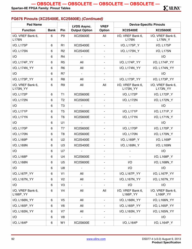
Spartan-IIE FPGA Family: Pinout TablesR
— OBSOLETE — OBSOLETE — OBSOLETE — OBSOLETE —
I/O, VREF Bank 6, L176N
6 P9 XC2S600E All I/O, VREF Bank 6, L176N
I/O, VREF Bank 6, L176N_Y
I/O, L175P 6 R1 XC2S400E - I/O, L175P_Y I/O, L175P
I/O, L175N 6 R2 XC2S400E - I/O, L175N_Y I/O, L175N
I/O 6 R4 - - - I/O
I/O, L174P_YY 6 R5 All - I/O, L174P_YY I/O, L174P_YY
I/O, L174N_YY 6 R6 All - I/O, L174N_YY I/O, L174N_YY
I/O 6 R7 - - - I/O
I/O, L173P_YY 6 R8 All - I/O, L173P_YY I/O, L173P_YY
I/O, VREF Bank 6, L173N_YY
6 R9 All All I/O, VREF Bank 6, L173N_YY
I/O, VREF Bank 6, L173N_YY
I/O, L172P 6 T1 XC2S600E - I/O, L172P I/O, L172P_Y
I/O, L172N 6 T2 XC2S600E - I/O, L172N I/O, L172N_Y
I/O 6 T3 - - - I/O
I/O, L171P 6 T5 XC2S600E - I/O, L171P I/O, L171P_Y
I/O, L171N 6 T6 XC2S600E - I/O, L171N I/O, L171N_Y
I/O 6 U1 - - - I/O
I/O, L170P 6 T7 XC2S600E - I/O, L170P I/O, L170P_Y
I/O, L170N 6 T8 XC2S600E - I/O, L170N I/O, L170N_Y
I/O, L169P 6 U2 XC2S400E - I/O, L169P_Y I/O, L169P
I/O, L169N 6 U3 XC2S400E - I/O, L169N_Y I/O, L169N
I/O 6 U7 - - - I/O
I/O, L168P 6 U4 XC2S600E - - I/O, L168P_Y
I/O, L168N 6 U5 XC2S600E - I/O I/O, L168N_Y
I/O 6 U8 - - I/O I/O
I/O, L167P_YY 6 V1 All - I/O, L167P_YY I/O, L167P_YY
I/O, L167N_YY 6 V2 All - I/O, L167N_YY I/O, L167N_YY
I/O 6 V3 - - I/O I/O
I/O, VREF Bank 6, L166P_YY
6 V4 All All I/O, VREF Bank 6, L166P_YY
I/O, VREF Bank 6, L166P_YY
I/O, L166N_YY 6 V5 All - I/O, L166N_YY I/O, L166N_YY
I/O, L165P_YY 6 V6 All - I/O, L165P_YY I/O, L165P_YY
I/O, L165N_YY 6 V7 All - I/O, L165N_YY I/O, L165N_YY
I/O 6 V8 - - - I/O
I/O, L164P 6 W1 XC2S600E - I/O, L164P I/O, L164P_Y
FG676 Pinouts (XC2S400E, XC2S600E) (Continued)Pad Name
PinLVDS Async.
Output OptionVREF Option
Device-Specific Pinouts
Function Bank XC2S400E XC2S600E
92 www.xilinx.com DS077-4 (v3.0) August 9, 2013Product Specification
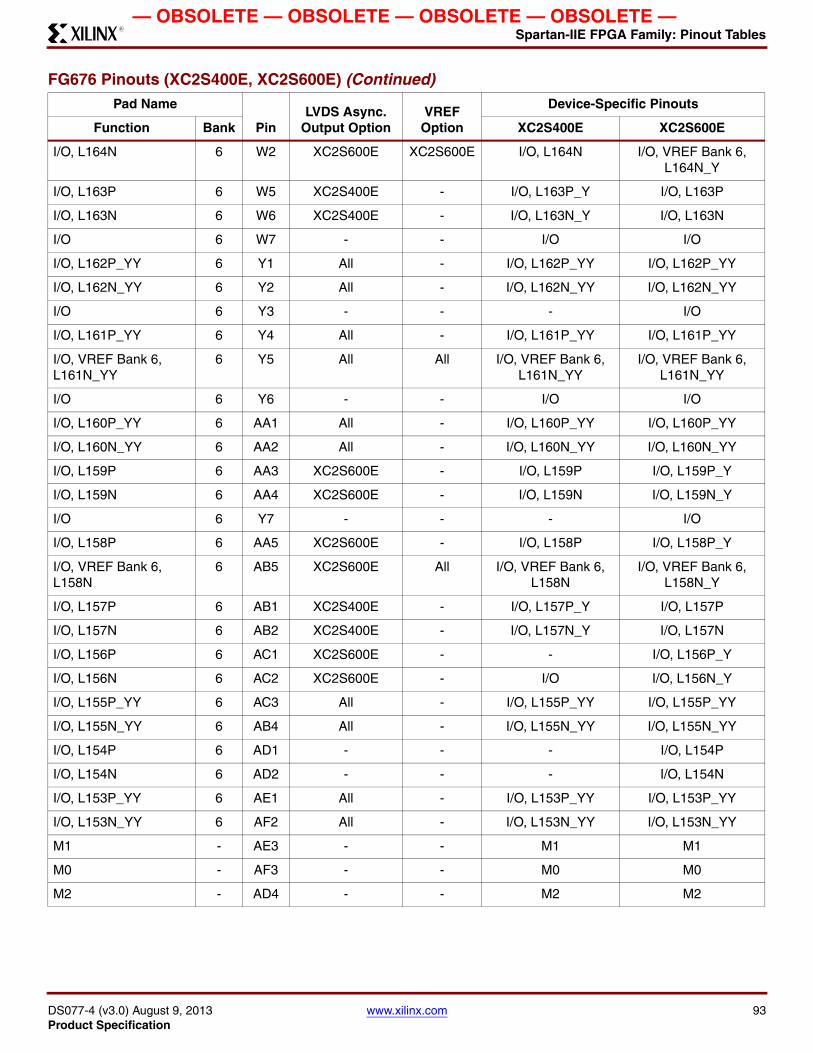
Spartan-IIE FPGA Family: Pinout TablesR
— OBSOLETE — OBSOLETE — OBSOLETE — OBSOLETE —
I/O, L164N 6 W2 XC2S600E XC2S600E I/O, L164N I/O, VREF Bank 6, L164N_Y
I/O, L163P 6 W5 XC2S400E - I/O, L163P_Y I/O, L163P
I/O, L163N 6 W6 XC2S400E - I/O, L163N_Y I/O, L163N
I/O 6 W7 - - I/O I/O
I/O, L162P_YY 6 Y1 All - I/O, L162P_YY I/O, L162P_YY
I/O, L162N_YY 6 Y2 All - I/O, L162N_YY I/O, L162N_YY
I/O 6 Y3 - - - I/O
I/O, L161P_YY 6 Y4 All - I/O, L161P_YY I/O, L161P_YY
I/O, VREF Bank 6, L161N_YY
6 Y5 All All I/O, VREF Bank 6, L161N_YY
I/O, VREF Bank 6, L161N_YY
I/O 6 Y6 - - I/O I/O
I/O, L160P_YY 6 AA1 All - I/O, L160P_YY I/O, L160P_YY
I/O, L160N_YY 6 AA2 All - I/O, L160N_YY I/O, L160N_YY
I/O, L159P 6 AA3 XC2S600E - I/O, L159P I/O, L159P_Y
I/O, L159N 6 AA4 XC2S600E - I/O, L159N I/O, L159N_Y
I/O 6 Y7 - - - I/O
I/O, L158P 6 AA5 XC2S600E - I/O, L158P I/O, L158P_Y
I/O, VREF Bank 6, L158N
6 AB5 XC2S600E All I/O, VREF Bank 6, L158N
I/O, VREF Bank 6, L158N_Y
I/O, L157P 6 AB1 XC2S400E - I/O, L157P_Y I/O, L157P
I/O, L157N 6 AB2 XC2S400E - I/O, L157N_Y I/O, L157N
I/O, L156P 6 AC1 XC2S600E - - I/O, L156P_Y
I/O, L156N 6 AC2 XC2S600E - I/O I/O, L156N_Y
I/O, L155P_YY 6 AC3 All - I/O, L155P_YY I/O, L155P_YY
I/O, L155N_YY 6 AB4 All - I/O, L155N_YY I/O, L155N_YY
I/O, L154P 6 AD1 - - - I/O, L154P
I/O, L154N 6 AD2 - - - I/O, L154N
I/O, L153P_YY 6 AE1 All - I/O, L153P_YY I/O, L153P_YY
I/O, L153N_YY 6 AF2 All - I/O, L153N_YY I/O, L153N_YY
M1 - AE3 - - M1 M1
M0 - AF3 - - M0 M0
M2 - AD4 - - M2 M2
FG676 Pinouts (XC2S400E, XC2S600E) (Continued)Pad Name
PinLVDS Async.
Output OptionVREF Option
Device-Specific Pinouts
Function Bank XC2S400E XC2S600E
DS077-4 (v3.0) August 9, 2013 www.xilinx.com 93Product Specification

Spartan-IIE FPGA Family: Pinout TablesR
— OBSOLETE — OBSOLETE — OBSOLETE — OBSOLETE —
I/O 5 AC5 - - I/O I/O
I/O, L152N 5 AE4 - - I/O I/O, L152N
I/O, L152P 5 AF4 - - - I/O, L152P
I/O, L151N 5 AE5 - - - I/O, L151N
I/O, L151P 5 AF5 - - I/O I/O, L151P
I/O, L150N 5 AA6 XC2S400E - I/O, L150N_Y I/O, L150N
I/O, L150P 5 AB6 XC2S400E - I/O, L150P_Y I/O, L150P
I/O, L149N_YY 5 AC6 All - I/O, L149N_YY I/O, L149N_YY
I/O, L149P_YY 5 AD6 All - I/O, L149P_YY I/O, L149P_YY
I/O, VREF Bank 5, L148N_YY
5 AE6 All All I/O, VREF Bank 5, L148N_YY
I/O, VREF Bank 5, L148N_YY
I/O, L148P_YY 5 AF6 All - I/O, L148P_YY I/O, L148P_YY
I/O, L147N 5 AA7 XC2S600E - - I/O, L147N_Y
I/O, L147P 5 AB7 XC2S600E - I/O I/O, L147P_Y
I/O, L146N_YY 5 AC7 All - I/O, L146N_YY I/O, L146N_YY
I/O, L146P_YY 5 AD7 All - I/O, L146P_YY I/O, L146P_YY
I/O, L145N_YY 5 AE7 All - I/O, L145N_YY I/O, L145N_YY
I/O, L145P_YY 5 AF7 All - I/O, L145P_YY I/O, L145P_YY
I/O, VREF Bank 5, L144N_YY
5 Y8 All All I/O, VREF Bank 5, L144N_YY
I/O, VREF Bank 5, L144N_YY
I/O, L144P_YY 5 AA8 All - I/O, L144P_YY I/O, L144P_YY
I/O, L143N_YY 5 AE8 All - I/O, L143N_YY I/O, L143N_YY
I/O, L143P_YY 5 AF8 All - I/O, L143P_YY I/O, L143P_YY
I/O 5 AB8 - - I/O I/O
I/O, L142N 5 W9 XC2S600E - I/O, L142N I/O, L142N_Y
I/O, L142P 5 Y9 XC2S600E - I/O, L142P I/O, L142P_Y
I/O, L141N 5 AA9 XC2S600E XC2S600E - I/O, VREF Bank 5, L141N_Y
I/O, L141P 5 AB9 XC2S600E - I/O I/O, L141P_Y
I/O, L140N_YY 5 AC9 All - I/O, L140N_YY I/O, L140N_YY
I/O, L140P_YY 5 AD9 All - I/O, L140P_YY I/O, L140P_YY
I/O, L139N_YY 5 AE9 All - I/O, L139N_YY I/O, L139N_YY
I/O, L139P_YY 5 AF9 All - I/O, L139P_YY I/O, L139P_YY
I/O, VREF Bank 5, L138N_YY
5 W10 All All I/O, VREF Bank 5, L138N_YY
I/O, VREF Bank 5, L138N_YY
FG676 Pinouts (XC2S400E, XC2S600E) (Continued)Pad Name
PinLVDS Async.
Output OptionVREF Option
Device-Specific Pinouts
Function Bank XC2S400E XC2S600E
94 www.xilinx.com DS077-4 (v3.0) August 9, 2013Product Specification
Spartan-IIE FPGA Family: Pinout TablesR
— OBSOLETE — OBSOLETE — OBSOLETE — OBSOLETE —
I/O, L138P_YY 5 Y10 All - I/O, L138P_YY I/O, L138P_YY
I/O, L137N_YY 5 AB10 All - I/O, L137N_YY I/O, L137N_YY
I/O, L137P_YY 5 AC10 All - I/O, L137P_YY I/O, L137P_YY
I/O 5 AD10 - - - I/O
I/O, L136N 5 AE10 XC2S600E - I/O, L136N I/O, L136N_Y
I/O, L136P 5 AF10 XC2S600E - I/O, L136P I/O, L136P_Y
I/O 5 AD11 - - - I/O
I/O, L135N_YY 5 W11 All - I/O, L135N_YY I/O, L135N_YY
I/O, L135P_YY 5 Y11 All - I/O, L135P_YY I/O, L135P_YY
I/O, L134N_YY 5 AA11 All - I/O, L134N_YY I/O, L134N_YY
I/O, L134P_YY 5 AB11 All - I/O, L134P_YY I/O, L134P_YY
I/O 5 V12 - - - I/O
I/O, L133N 5 AE11 - - I/O, L133N I/O, L133N
I/O, L133P 5 AF11 - - I/O, L133P I/O, L133P
I/O 5 W12 - - - I/O
I/O, L132N_YY 5 Y12 All - I/O, L132N_YY I/O, L132N_YY
I/O, L132P_YY 5 AA12 All - I/O, L132P_YY I/O, L132P_YY
I/O, VREF Bank 5, L131N_YY
5 AB12 All All I/O, VREF Bank 5, L131N_YY
I/O, VREF Bank 5, L131N_YY
I/O, L131P_YY 5 AC12 All - I/O, L131P_YY I/O, L131P_YY
I/O 5 V13 - - - I/O
I/O, L130N_YY 5 AE12 All - I/O, L130N_YY I/O, L130N_YY
I/O, L130P_YY 5 AF12 All - I/O, L130P_YY I/O, L130P_YY
I/O 5 W13 - - - I/O
I/O, L129N 5 Y13 XC2S600E - I/O, L129N I/O, L129N_Y
I/O, L129P 5 AA13 XC2S600E - I/O, L129P I/O, L129P_Y
I/O, VREF Bank 5, L128N
5 AB13 XC2S600E All I/O, VREF Bank 5, L128N
I/O, VREF Bank 5, L128N_Y
I/O, L128P 5 AC13 XC2S600E - I/O, L128P I/O, L128P_Y
I/O 5 AD13 - - - I/O
I/O, L127N 5 V14 - - I/O I/O, L127N
I/O, L127P 5 W14 - - - I/O, L127P
I/O (DLL), L126N 5 AE13 - - I/O (DLL), L126N I/O (DLL), L126N
GCK1, I 5 AF13 - - GCK1, I GCK1, I
FG676 Pinouts (XC2S400E, XC2S600E) (Continued)Pad Name
PinLVDS Async.
Output OptionVREF Option
Device-Specific Pinouts
Function Bank XC2S400E XC2S600E
DS077-4 (v3.0) August 9, 2013 www.xilinx.com 95Product Specification
Spartan-IIE FPGA Family: Pinout TablesR
— OBSOLETE — OBSOLETE — OBSOLETE — OBSOLETE —
GCK0, I 4 AF14 - - GCK0, I GCK0, I
I/O (DLL), L126P 4 AE14 - - I/O (DLL), L126P I/O (DLL), L126P
I/O 4 AD14 - - - I/O
I/O, L125N 4 AC14 - - I/O, L125N I/O, L125N
I/O, L125P 4 AB14 - - I/O, L125P I/O, L125P
I/O 4 AC15 - - - I/O
I/O, L124N 4 AA14 XC2S600E - I/O, L124N I/O, L124N_Y
I/O, VREF Bank 4, L124P
4 Y14 XC2S600E All I/O, VREF Bank 4, L124P
I/O, VREF Bank 4, L124P_Y
I/O, L123N 4 AF15 XC2S600E - I/O, L123N I/O, L123N_Y
I/O, L123P 4 AE15 XC2S600E - I/O, L123P I/O, L123P_Y
I/O 4 AB15 - - - I/O
I/O, L122N_YY 4 AA15 All - I/O, L122N_YY I/O, L122N_YY
I/O, L122P_YY 4 Y15 All - I/O, L122P_YY I/O, L122P_YY
I/O 4 AF16 - - - I/O
I/O, L121N_YY 4 W15 All - I/O, L121N_YY I/O, L121N_YY
I/O, VREF Bank 4, L121P_YY
4 V15 All All I/O, VREF Bank 4, L121P_YY
I/O, VREF Bank 4, L121P_YY
I/O, L120N_YY 4 AE16 All - I/O, L120N_YY I/O, L120N_YY
I/O, L120P_YY 4 AD16 All - I/O, L120P_YY I/O, L120P_YY
I/O 4 AB16 - - - I/O
I/O, L119N 4 AA16 - - I/O, L119N I/O, L119N
I/O, L119P 4 Y16 - - I/O, L119P I/O, L119P
I/O 4 W16 - - - I/O
I/O, L118N_YY 4 AF17 All - I/O, L118N_YY I/O, L118N_YY
I/O, L118P_YY 4 AE17 All - I/O, L118P_YY I/O, L118P_YY
I/O, L117N_YY 4 AD17 All - I/O, L117N_YY I/O, L117N_YY
I/O, L117P_YY 4 AC17 All - I/O, L117P_YY I/O, L117P_YY
I/O 4 AB17 - - - I/O
I/O, L116N 4 Y17 XC2S600E - I/O, L116N I/O, L116N_Y
I/O, L116P 4 W17 XC2S600E - I/O, L116P I/O, L116P_Y
I/O 4 AF18 - - - I/O
I/O, L115N_YY 4 AE18 All - I/O, L115N_YY I/O, L115N_YY
I/O, L115P_YY 4 AD18 All - I/O, L115P_YY I/O, L115P_YY
FG676 Pinouts (XC2S400E, XC2S600E) (Continued)Pad Name
PinLVDS Async.
Output OptionVREF Option
Device-Specific Pinouts
Function Bank XC2S400E XC2S600E
96 www.xilinx.com DS077-4 (v3.0) August 9, 2013Product Specification

Spartan-IIE FPGA Family: Pinout TablesR
— OBSOLETE — OBSOLETE — OBSOLETE — OBSOLETE —
I/O 4 AC18 - - I/O I/O
I/O, VREF Bank 4, L114N
4 AB18 - All I/O, VREF Bank 4, L114N
I/O, VREF Bank 4, L114N
I/O, L114P 4 AA18 - - I/O, L114P I/O, L114P
I/O, L113N 4 Y18 - - I/O, L113N I/O, L113N
I/O, L113P 4 W18 - - I/O, L113P I/O, L113P
I/O 4 AB19 - - I/O I/O
I/O, L112N 4 AF19 XC2S600E - I/O I/O, L112N_Y
I/O, L112P 4 AE19 XC2S600E XC2S600E - I/O, VREF Bank 4, L112P_Y
I/O, L111N 4 AA19 XC2S600E - I/O, L111N I/O, L111N_Y
I/O, L111P 4 Y19 XC2S600E - I/O, L111P I/O, L111P_Y
I/O 4 AF20 - - - I/O
I/O, L110N 4 AE20 XC2S600E - I/O, L110N I/O, L110N_Y
I/O, L110P 4 AD20 XC2S600E - I/O, L110P I/O, L110P_Y
I/O 4 AC20 - - I/O I/O
I/O, L109N_YY 4 AB20 All - I/O, L109N_YY I/O, L109N_YY
I/O, VREF Bank 4, L109P_YY
4 AA20 All All I/O, VREF Bank 4, L109P_YY
I/O, VREF Bank 4, L109P_YY
I/O 4 Y20 - - I/O I/O
I/O, L108N 4 AF21 - - I/O, L108N I/O, L108N
I/O, L108P 4 AE21 - - I/O, L108P I/O, L108P
I/O, L107N 4 AD21 - - I/O, L107N I/O, L107N
I/O, L107P 4 AC21 - - I/O, L107P I/O, L107P
I/O 4 AC22 - - - I/O
I/O, L106N_YY 4 AF22 All - I/O, L106N_YY I/O, L106N_YY
I/O, VREF Bank 4, L106P_YY
4 AE22 All All I/O, VREF Bank 4, L106P_YY
I/O, VREF Bank 4, L106P_YY
I/O, L105N_YY 4 AB21 All - I/O, L105N_YY I/O, L105N_YY
I/O, L105P_YY 4 AA21 All - I/O, L105P_YY I/O, L105P_YY
I/O, L104N_YY 4 AF23 All - I/O, L104N_YY I/O, L104N_YY
I/O, L104P_YY 4 AE23 All - I/O, L104P_YY I/O, L104P_YY
I/O, L103N 4 AD23 XC2S600E - I/O I/O, L103N_Y
I/O, L103P 4 AE24 XC2S600E - - I/O, L103P_Y
I/O, L102N_YY 4 AF24 All - I/O, L102N_YY I/O, L102N_YY
I/O, L102P_YY 4 AF25 All - I/O, L102P_YY I/O, L102P_YY
FG676 Pinouts (XC2S400E, XC2S600E) (Continued)Pad Name
PinLVDS Async.
Output OptionVREF Option
Device-Specific Pinouts
Function Bank XC2S400E XC2S600E
DS077-4 (v3.0) August 9, 2013 www.xilinx.com 97Product Specification
Spartan-IIE FPGA Family: Pinout TablesR
— OBSOLETE — OBSOLETE — OBSOLETE — OBSOLETE —
DONE 3 AE26 - - DONE DONE
PROGRAM - AC24 - - PROGRAM PROGRAM
I/O (INIT), L101N_YY 3 AD25 All - I/O (INIT), L101N_YY I/O (INIT), L101N_YY
I/O (D7), L101P_YY 3 AD26 All - I/O (D7), L101P_YY I/O (D7), L101P_YY
I/O, L100N 3 AC25 - - - I/O, L100N
I/O, L100P 3 AC26 - - - I/O, L100P
I/O, L99N 3 AB22 XC2S600E - - I/O, L99N_Y
I/O, L99P 3 AB23 XC2S600E - I/O I/O, L99P_Y
I/O, L98N_YY 3 AB25 All - I/O, L98N_YY I/O, L98N_YY
I/O, L98P_YY 3 AB26 All - I/O, L98P_YY I/O, L98P_YY
I/O, L97N 3 AA23 - - I/O, L97N_Y I/O, L97N
I/O, L97P 3 AA24 - - I/O, L97P_Y I/O, L97P
I/O, VREF Bank 3, L96N
3 AA25 XC2S600E All I/O, VREF Bank 3, L96N
I/O, VREF Bank 3, L96N_Y
I/O, L96P 3 AA26 XC2S600E - I/O, L96P I/O, L96P_Y
I/O, L95N 3 AA22 XC2S600E - - I/O, L95N_Y
I/O, L95P 3 Y22 XC2S600E - I/O I/O, L95P_Y
I/O, L94N 3 Y23 XC2S400E - I/O, L94N_Y I/O, L94N
I/O, L94P 3 Y24 XC2S400E - I/O, L94P_Y I/O, L94P
I/O, L93N 3 Y25 XC2S600E - I/O, L93N I/O, L93N_Y
I/O, L93P 3 Y26 XC2S600E - I/O, L93P I/O, L93P_Y
I/O, VREF Bank 3, L92N_YY
3 W21 All All I/O, VREF Bank 3, L92N_YY
I/O, VREF Bank 3, L92N_YY
I/O, L92P_YY 3 W22 All - I/O, L92P_YY I/O, L92P_YY
I/O 3 Y21 - - - I/O
I/O, L91N_YY 3 W25 All - I/O, L91N_YY I/O, L91N_YY
I/O, L91P_YY 3 W26 All - I/O, L91P_YY I/O, L91P_YY
I/O 3 W20 - - I/O I/O
I/O, L90N 3 V19 XC2S400E - I/O, L90N_Y I/O, L90N
I/O, L90P 3 V20 XC2S400E - I/O, L90P_Y I/O, L90P
I/O, L89N 3 V21 XC2S600E XC2S600E - I/O, VREF Bank 3, L89N_Y
I/O, L89P 3 V22 XC2S600E - I/O I/O, L89P_Y
I/O 3 V23 - - I/O I/O
I/O, L88N_YY 3 V24 All - I/O, L88N_YY I/O, L88N_YY
FG676 Pinouts (XC2S400E, XC2S600E) (Continued)Pad Name
PinLVDS Async.
Output OptionVREF Option
Device-Specific Pinouts
Function Bank XC2S400E XC2S600E
98 www.xilinx.com DS077-4 (v3.0) August 9, 2013Product Specification
Spartan-IIE FPGA Family: Pinout TablesR
— OBSOLETE — OBSOLETE — OBSOLETE — OBSOLETE —
I/O, L88P_YY 3 V25 All - I/O, L88P_YY I/O, L88P_YY
I/O 3 V26 - - I/O I/O
I/O, VREF Bank 3, L87N_YY
3 U19 All All I/O, VREF Bank 3, L87N_YY
I/O, VREF Bank 3, L87N_YY
I/O (D6), L87P_YY 3 U20 All - I/O (D6), L87P_YY I/O (D6), L87P_YY
I/O (D5), L86N_YY 3 U22 All - I/O (D5), L86N_YY I/O (D5), L86N_YY
I/O, L86P_YY 3 U23 All - I/O, L86P_YY I/O, L86P_YY
I/O 3 U24 - - - I/O
I/O, L85N 3 U25 XC2S600E - - I/O, L85N_Y
I/O, L85P 3 U26 XC2S600E - I/O I/O, L85P_Y
I/O 3 R18 - - I/O I/O
I/O, L84N 3 T19 XC2S400E - I/O, L84N_Y I/O, L84N
I/O, L84P 3 T20 XC2S400E - I/O, L84P_Y I/O, L84P
I/O, L83N 3 T21 XC2S600E - I/O, L83N I/O, L83N_Y
I/O, L83P 3 T22 XC2S600E - I/O, L83P I/O, L83P_Y
I/O 3 T24 - - - I/O
I/O, L82N 3 T25 XC2S600E - I/O, L82N I/O, L82N_Y
I/O, L82P 3 T26 XC2S600E - I/O, L82P I/O, L82P_Y
I/O 3 R19 - - - I/O
I/O, L81N 3 R20 XC2S600E - I/O, L81N I/O, L81N_Y
I/O, L81P 3 R21 XC2S600E - I/O, L81P I/O, L81P_Y
I/O, VREF Bank 3, L80N_YY
3 R22 All All I/O, VREF Bank 3, L80N_YY
I/O, VREF Bank 3, L80N_YY
I/O (D4), L80P_YY 3 R23 All - I/O (D4), L80P_YY I/O (D4), L80P_YY
I/O 3 P18 - - - I/O
I/O, L79N_YY 3 R25 All - I/O, L79N_YY I/O, L79N_YY
I/O, L79P_YY 3 R26 All - I/O, L79P_YY I/O, L79P_YY
I/O 3 P19 - - - I/O
I/O, L78N 3 P20 XC2S400E - I/O, L78N_Y I/O, L78N
I/O, L78P 3 P21 XC2S400E - I/O, L78P_Y I/O, L78P
I/O, VREF Bank 3, L77N
3 P22 XC2S600E All I/O, VREF Bank 3, L77N
I/O, VREF Bank 3, L77N_Y
I/O, L77P 3 P23 XC2S600E - I/O, L77P I/O, L77P_Y
I/O 3 P24 - - - I/O
I/O, L76N_YY 3 P25 All - I/O, L76N_YY I/O, L76N_YY
I/O, L76P_YY 3 P26 All - I/O, L76P_YY I/O, L76P_YY
FG676 Pinouts (XC2S400E, XC2S600E) (Continued)Pad Name
PinLVDS Async.
Output OptionVREF Option
Device-Specific Pinouts
Function Bank XC2S400E XC2S600E
DS077-4 (v3.0) August 9, 2013 www.xilinx.com 99Product Specification

Spartan-IIE FPGA Family: Pinout TablesR
— OBSOLETE — OBSOLETE — OBSOLETE — OBSOLETE —
I/O 3 N18 - - - I/O
I/O (TRDY) 3 N24 - - I/O (TRDY) I/O (TRDY)
I/O (IRDY), L75N_YY 2 N26 All - I/O (IRDY), L75N_YY I/O (IRDY), L75N_YY
I/O, L75P_YY 2 N25 All - I/O, L75P_YY I/O, L75P_YY
I/O 2 N19 - - - I/O
I/O, L74N 2 N23 XC2S600E - - I/O, L74N_Y
I/O, L74P 2 N22 XC2S600E - I/O I/O, L74P_Y
I/O 2 M23 - - I/O I/O
I/O, L73N 2 N21 XC2S600E - I/O, L73N I/O, L73N_Y
I/O, VREF Bank 2, L73P
2 N20 XC2S600E All I/O, VREF Bank 2, L73P
I/O, VREF Bank 2, L73P_Y
I/O, L72N 2 M26 XC2S400E - I/O, L72N_Y I/O, L72N
I/O, L72P 2 M25 XC2S400E - I/O, L72P_Y I/O, L72P
I/O 2 M22 - - - I/O
I/O, L71N_YY 2 M21 All - I/O, L71N_YY I/O, L71N_YY
I/O, L71P_YY 2 M20 All - I/O, L71P_YY I/O, L71P_YY
I/O 2 L26 - - - I/O
I/O (D3), L70N_YY 2 M19 All - I/O (D3), L70N_YY I/O (D3), L70N_YY
I/O, VREF Bank 2, L70P_YY
2 M18 All All I/O, VREF Bank 2, L70P_YY
I/O, VREF Bank 2, L70P_YY
I/O, L69N 2 L25 XC2S600E - I/O, L69N I/O, L69N_Y
I/O, L69P 2 L24 XC2S600E - I/O, L69P I/O, L69P_Y
I/O 2 L22 - - - I/O
I/O, L68N 2 L21 XC2S600E - I/O, L68N I/O, L68N_Y
I/O, L68P 2 L20 XC2S600E - I/O, L68P I/O, L68P_Y
I/O 2 L19 - - - I/O
I/O, L67N 2 K26 XC2S600E - I/O, L67N I/O, L67N_Y
I/O, L67P 2 K25 XC2S600E - I/O, L67P I/O, L67P_Y
I/O, L66N 2 K24 - - - I/O, L66N
I/O, L66P 2 K23 - - I/O I/O, L66P
I/O 2 K22 - - - I/O
I/O, L65N 2 K20 XC2S600E - I/O I/O, L65N_Y
I/O, L65P 2 K19 XC2S600E - I/O I/O, L65P_Y
I/O 2 J26 - - I/O I/O
FG676 Pinouts (XC2S400E, XC2S600E) (Continued)Pad Name
PinLVDS Async.
Output OptionVREF Option
Device-Specific Pinouts
Function Bank XC2S400E XC2S600E
100 www.xilinx.com DS077-4 (v3.0) August 9, 2013Product Specification
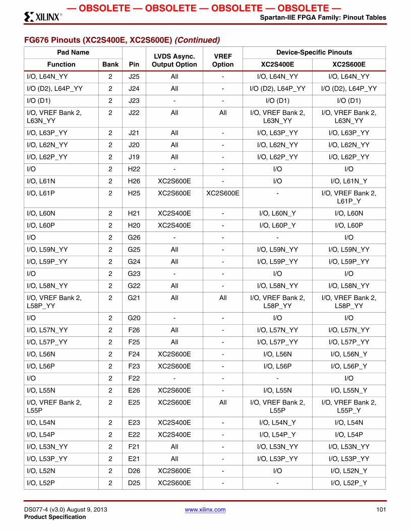
Spartan-IIE FPGA Family: Pinout TablesR
— OBSOLETE — OBSOLETE — OBSOLETE — OBSOLETE —
I/O, L64N_YY 2 J25 All - I/O, L64N_YY I/O, L64N_YY
I/O (D2), L64P_YY 2 J24 All - I/O (D2), L64P_YY I/O (D2), L64P_YY
I/O (D1) 2 J23 - - I/O (D1) I/O (D1)
I/O, VREF Bank 2, L63N_YY
2 J22 All All I/O, VREF Bank 2, L63N_YY
I/O, VREF Bank 2, L63N_YY
I/O, L63P_YY 2 J21 All - I/O, L63P_YY I/O, L63P_YY
I/O, L62N_YY 2 J20 All - I/O, L62N_YY I/O, L62N_YY
I/O, L62P_YY 2 J19 All - I/O, L62P_YY I/O, L62P_YY
I/O 2 H22 - - I/O I/O
I/O, L61N 2 H26 XC2S600E - I/O I/O, L61N_Y
I/O, L61P 2 H25 XC2S600E XC2S600E - I/O, VREF Bank 2, L61P_Y
I/O, L60N 2 H21 XC2S400E - I/O, L60N_Y I/O, L60N
I/O, L60P 2 H20 XC2S400E - I/O, L60P_Y I/O, L60P
I/O 2 G26 - - - I/O
I/O, L59N_YY 2 G25 All - I/O, L59N_YY I/O, L59N_YY
I/O, L59P_YY 2 G24 All - I/O, L59P_YY I/O, L59P_YY
I/O 2 G23 - - I/O I/O
I/O, L58N_YY 2 G22 All - I/O, L58N_YY I/O, L58N_YY
I/O, VREF Bank 2, L58P_YY
2 G21 All All I/O, VREF Bank 2, L58P_YY
I/O, VREF Bank 2, L58P_YY
I/O 2 G20 - - I/O I/O
I/O, L57N_YY 2 F26 All - I/O, L57N_YY I/O, L57N_YY
I/O, L57P_YY 2 F25 All - I/O, L57P_YY I/O, L57P_YY
I/O, L56N 2 F24 XC2S600E - I/O, L56N I/O, L56N_Y
I/O, L56P 2 F23 XC2S600E - I/O, L56P I/O, L56P_Y
I/O 2 F22 - - - I/O
I/O, L55N 2 E26 XC2S600E - I/O, L55N I/O, L55N_Y
I/O, VREF Bank 2, L55P
2 E25 XC2S600E All I/O, VREF Bank 2, L55P
I/O, VREF Bank 2, L55P_Y
I/O, L54N 2 E23 XC2S400E - I/O, L54N_Y I/O, L54N
I/O, L54P 2 E22 XC2S400E - I/O, L54P_Y I/O, L54P
I/O, L53N_YY 2 F21 All - I/O, L53N_YY I/O, L53N_YY
I/O, L53P_YY 2 E21 All - I/O, L53P_YY I/O, L53P_YY
I/O, L52N 2 D26 XC2S600E - I/O I/O, L52N_Y
I/O, L52P 2 D25 XC2S600E - - I/O, L52P_Y
FG676 Pinouts (XC2S400E, XC2S600E) (Continued)Pad Name
PinLVDS Async.
Output OptionVREF Option
Device-Specific Pinouts
Function Bank XC2S400E XC2S600E
DS077-4 (v3.0) August 9, 2013 www.xilinx.com 101Product Specification

Spartan-IIE FPGA Family: Pinout TablesR
— OBSOLETE — OBSOLETE — OBSOLETE — OBSOLETE —
I/O, L51N 2 D24 - - - I/O, L51N
I/O, L51P 2 C25 - - - I/O, L51P
I/O (DIN, D0), L50N_YY
2 C26 All - I/O (DIN, D0), L50N_YY
I/O (DIN, D0), L50N_YY
I/O (DOUT, BUSY), L50P_YY
2 B26 All - I/O (DOUT, BUSY), L50P_YY
I/O (DOUT, BUSY), L50P_YY
CCLK 2 A25 - - CCLK CCLK
TDO 2 C23 - - TDO TDO
TDI - D22 - - TDI TDI
I/O (CS), L49P_YY 1 B24 All - I/O (CS), L49P_YY I/O (CS), L49P_YY
I/O (WRITE), L49N_YY 1 A24 All - I/O (WRITE), L49N_YY
I/O (WRITE), L49N_YY
I/O, L48P 1 B23 - - I/O I/O, L48P
I/O, L48N 1 A23 - - - I/O, L48N
I/O, L47P 1 B22 XC2S400E - I/O, L47P_Y I/O, L47P
I/O, L47N 1 A22 XC2S400E - I/O, L47N_Y I/O, L47N
I/O, L46P_YY 1 D21 All - I/O, L46P_YY I/O, L46P_YY
I/O, L46N_YY 1 C21 All - I/O, L46N_YY I/O, L46N_YY
I/O, VREF Bank 1, L45P_YY
1 B21 All All I/O, VREF Bank 1, L45P_YY
I/O, VREF Bank 1, L45P_YY
I/O, L45N_YY 1 A21 All - I/O, L45N_YY I/O, L45N_YY
I/O, L44P 1 F20 XC2S600E - - I/O, L44P_Y
I/O, L44N 1 E20 XC2S600E - I/O I/O, L44N_Y
I/O, L43P_YY 1 D20 All - I/O, L43P_YY I/O, L43P_YY
I/O, L43N_YY 1 C20 All - I/O, L43N_YY I/O, L43N_YY
I/O, L42P_YY 1 B20 All - I/O, L42P_YY I/O, L42P_YY
I/O, L42N_YY 1 A20 All - I/O, L42N_YY I/O, L42N_YY
I/O, VREF Bank 1, L41P_YY
1 G19 All All I/O, VREF Bank 1, L41P_YY
I/O, VREF Bank 1, L41P_YY
I/O, L41N_YY 1 F19 All - I/O, L41N_YY I/O, L41N_YY
I/O 1 E19 - - - I/O
I/O, L40P_YY 1 B19 All - I/O, L40P_YY I/O, L40P_YY
I/O, L40N_YY 1 A19 All - I/O, L40N_YY I/O, L40N_YY
I/O 1 H18 - - I/O I/O
I/O, L39P 1 G18 XC2S600E - I/O, L39P I/O, L39P_Y
FG676 Pinouts (XC2S400E, XC2S600E) (Continued)Pad Name
PinLVDS Async.
Output OptionVREF Option
Device-Specific Pinouts
Function Bank XC2S400E XC2S600E
102 www.xilinx.com DS077-4 (v3.0) August 9, 2013Product Specification

Spartan-IIE FPGA Family: Pinout TablesR
— OBSOLETE — OBSOLETE — OBSOLETE — OBSOLETE —
I/O, L39N 1 F18 XC2S600E - I/O, L39N I/O, L39N_Y
I/O, L38P 1 D18 XC2S600E XC2S600E - I/O, VREF Bank 1, L38P_Y
I/O, L38N 1 C18 XC2S600E - I/O I/O, L38N_Y
I/O, L37P_YY 1 B18 All - I/O, L37P_YY I/O, L37P_YY
I/O, L37N_YY 1 A18 All - I/O, L37N_YY I/O, L37N_YY
I/O, L36P_YY 1 H17 All - I/O, L36P_YY I/O, L36P_YY
I/O, L36N_YY 1 G17 All - I/O, L36N_YY I/O, L36N_YY
I/O, VREF Bank 1, L35P_YY
1 E18 All All I/O, VREF Bank 1, L35P_YY
I/O, VREF Bank 1, L35P_YY
I/O, L35N_YY 1 E17 All - I/O, L35N_YY I/O, L35N_YY
I/O, L34P_YY 1 D17 All - I/O, L34P_YY I/O, L34P_YY
I/O, L34N_YY 1 C17 All - I/O, L34N_YY I/O, L34N_YY
I/O 1 H16 - - - I/O
I/O, L33P 1 B17 XC2S600E - I/O, L33P I/O, L33P_Y
I/O, L33N 1 A17 XC2S600E - I/O, L33N I/O, L33N_Y
I/O 1 G16 - - - I/O
I/O, L32P_YY 1 F16 All - I/O, L32P_YY I/O, L32P_YY
I/O, L32N_YY 1 E16 All - I/O, L32N_YY I/O, L32N_YY
I/O, L31P_YY 1 C16 All - I/O, L31P_YY I/O, L31P_YY
I/O, L31N_YY 1 B16 All - I/O, L31N_YY I/O, L31N_YY
I/O 1 A16 - - - I/O
I/O, L30P 1 J15 - - I/O, L30P I/O, L30P
I/O, L30N 1 H15 - - I/O, L30N I/O, L30N
I/O 1 G15 - - - I/O
I/O, L29P_YY 1 F15 All - I/O, L29P_YY I/O, L29P_YY
I/O, L29N_YY 1 E15 All - I/O, L29N_YY I/O, L29N_YY
I/O, VREF Bank 1, L28P_YY
1 B15 All All I/O, VREF Bank 1, L28P_YY
I/O, VREF Bank 1, L28P_YY
I/O, L28N_YY 1 A15 All - I/O, L28N_YY I/O, L28N_YY
I/O 1 D15 - - - I/O
I/O, L27P_YY 1 J14 All - I/O, L27P_YY I/O, L27P_YY
I/O, L27N_YY 1 H14 All - I/O, L27N_YY I/O, L27N_YY
I/O 1 G14 - - - I/O
I/O, L26P 1 F14 XC2S600E - I/O, L26P I/O, L26P_Y
I/O, L26N 1 E14 XC2S600E - I/O, L26N I/O, L26N_Y
FG676 Pinouts (XC2S400E, XC2S600E) (Continued)Pad Name
PinLVDS Async.
Output OptionVREF Option
Device-Specific Pinouts
Function Bank XC2S400E XC2S600E
DS077-4 (v3.0) August 9, 2013 www.xilinx.com 103Product Specification

Spartan-IIE FPGA Family: Pinout TablesR
— OBSOLETE — OBSOLETE — OBSOLETE — OBSOLETE —
I/O, VREF Bank 1, L25P
1 D14 XC2S600E All I/O, VREF Bank 1, L25P
I/O, VREF Bank 1, L25P_Y
I/O, L25N 1 C14 XC2S600E - I/O, L25N I/O, L25N_Y
I/O 1 J13 - - - I/O
I/O, L24P 1 C13 - - I/O, L24P I/O, L24P
I/O, L24N 1 D13 - - I/O, L24N I/O, L24N
I/O 1 H13 - - - I/O
I/O (DLL), L23P 1 B14 - - I/O (DLL), L23P I/O (DLL), L23P
GCK2, I 1 A14 - - GCK2, I GCK2, I
GCK3, I 0 A13 - - GCK3, I GCK3, I
I/O (DLL), L23N 0 B13 - - I/O (DLL), L23N I/O (DLL), L23N
I/O 0 E13 - - - I/O
I/O, L22P_YY 0 F13 All - I/O, L22P_YY I/O, L22P_YY
I/O, L22N_YY 0 G13 All - I/O, L22N_YY I/O, L22N_YY
I/O, L21P 0 A12 XC2S600E - - I/O, L21P_Y
I/O, VREF Bank 0, L21N
0 B12 XC2S600E All I/O, VREF Bank 0 I/O, VREF Bank 0, L21N_Y
I/O, L20P 0 D12 XC2S600E - I/O, L20P I/O, L20P_Y
I/O, L20N 0 E12 XC2S600E - I/O, L20N I/O, L20N_Y
I/O 0 F12 - - - I/O
I/O, L19P_YY 0 G12 All - I/O, L19P_YY I/O, L19P_YY
I/O, L19N_YY 0 H12 All - I/O, L19N_YY I/O, L19N_YY
I/O 0 J12 - - - I/O
I/O, L18P_YY 0 A11 All - I/O, L18P_YY I/O, L18P_YY
I/O, VREF Bank 0, L18N_YY
0 B11 All All I/O, VREF Bank 0, L18N_YY
I/O, VREF Bank 0, L18N_YY
I/O, L17P_YY 0 E11 All - I/O, L17P_YY I/O, L17P_YY
I/O, L17N_YY 0 F11 All - I/O, L17N_YY I/O, L17N_YY
I/O 0 C11 - - - I/O
I/O, L16P 0 G11 - - I/O, L16P I/O, L16P
I/O, L16N 0 H11 - - I/O, L16N I/O, L16N
I/O 0 C10 - - - I/O
I/O, L15P_YY 0 A10 All - I/O, L15P_YY I/O, L15P_YY
I/O, L15N_YY 0 B10 All - I/O, L15N_YY I/O, L15N_YY
I/O, L14P_YY 0 D10 All - I/O, L14P_YY I/O, L14P_YY
FG676 Pinouts (XC2S400E, XC2S600E) (Continued)Pad Name
PinLVDS Async.
Output OptionVREF Option
Device-Specific Pinouts
Function Bank XC2S400E XC2S600E
104 www.xilinx.com DS077-4 (v3.0) August 9, 2013Product Specification

Spartan-IIE FPGA Family: Pinout TablesR
— OBSOLETE — OBSOLETE — OBSOLETE — OBSOLETE —
I/O, L14N_YY 0 E10 All - I/O, L14N_YY I/O, L14N_YY
I/O 0 G10 - - - I/O
I/O, L13P 0 A9 XC2S600E - I/O, L13P I/O, L13P_Y
I/O, L13N 0 B9 XC2S600E - I/O, L13N I/O, L13N_Y
I/O 0 H10 - - - I/O
I/O, L12P_YY 0 C9 All - I/O, L12P_YY I/O, L12P_YY
I/O, L12N_YY 0 D9 All - I/O, L12N_YY I/O, L12N_YY
I/O 0 E9 - - I/O I/O
I/O, VREF Bank 0, L11P
0 F9 - All I/O, VREF Bank 0, L11P
I/O, VREF Bank 0, L11P
I/O, L11N 0 G9 - - I/O, L11N I/O, L11N
I/O, L10P 0 A8 - - I/O, L10P I/O, L10P
I/O, L10N 0 B8 - - I/O, L10N I/O, L10N
I/O 0 H9 - - I/O I/O
I/O, L9P 0 E8 XC2S600E - I/O I/O, L9P_Y
I/O, L9N 0 F8 XC2S600E XC2S600E - I/O, VREF Bank 0, L9N_Y
I/O, L8P 0 A7 XC2S600E - I/O, L8P I/O, L8P_Y
I/O, L8N 0 B7 XC2S600E - I/O, L8N I/O, L8N_Y
I/O 0 G8 - - I/O I/O
I/O, L7P_YY 0 C7 All - I/O, L7P_YY I/O, L7P_YY
I/O, L7N_YY 0 D7 All - I/O, L7N_YY I/O, L7N_YY
I/O 0 E7 - - - I/O
I/O, L6P_YY 0 F7 All - I/O, L6P_YY I/O, L6P_YY
I/O, VREF Bank 0, L6N_YY
0 G7 All All I/O, VREF Bank 0, L6N_YY
I/O, VREF Bank 0, L6N_YY
I/O 0 A6 - - I/O I/O
I/O, L5P 0 B6 - - I/O, L5P I/O, L5P
I/O, L5N 0 C6 - - I/O, L5N I/O, L5N
I/O, L4P 0 D6 - - I/O, L4P I/O, L4P
I/O, L4N 0 E6 - - I/O, L4N I/O, L4N
I/O 0 F6 - - - I/O
I/O, L3P_YY 0 A5 All - I/O, L3P_YY I/O, L3P_YY
I/O, VREF Bank 0, L3N_YY
0 B5 All All I/O, VREF Bank 0, L3N_YY
I/O, VREF Bank 0, L3N_YY
I/O, L2P_YY 0 D5 All - I/O, L2P_YY I/O, L2P_YY
FG676 Pinouts (XC2S400E, XC2S600E) (Continued)Pad Name
PinLVDS Async.
Output OptionVREF Option
Device-Specific Pinouts
Function Bank XC2S400E XC2S600E
DS077-4 (v3.0) August 9, 2013 www.xilinx.com 105Product Specification

Spartan-IIE FPGA Family: Pinout TablesR
— OBSOLETE — OBSOLETE — OBSOLETE — OBSOLETE —
I/O, L2N_YY 0 E5 All - I/O, L2N_YY I/O, L2N_YY
I/O, L1P_YY 0 B4 All - I/O, L1P_YY I/O, L1P_YY
I/O, L1N_YY 0 C4 All - I/O, L1N_YY I/O, L1N_YY
I/O, L0P 0 A3 XC2S600E - I/O I/O, L0P_Y
I/O, L0N 0 B3 XC2S600E - - I/O, L0N_Y
I/O 0 A4 - - I/O I/O
TCK - A2 - - TCK TCK
FG676 Differential Clock Pins
Clock Bank
P Input N Input
Pin Name Pin Name
GCK0 4 AF14 GCK0, I AE14 I/O (DLL), L126P
GCK1 5 AF13 GCK1, I AE13 I/O (DLL), L126N
GCK2 1 A14 GCK2, I B14 I/O (DLL), L23P
GCK3 0 A13 GCK3, I B13 I/O (DLL), L23N
FG676 Pinouts (XC2S400E, XC2S600E) (Continued)Pad Name
PinLVDS Async.
Output OptionVREF Option
Device-Specific Pinouts
Function Bank XC2S400E XC2S600E
Additional FG676 Package Pins VCCINT Pins
H8 H19 J9 J18 K10 K11 K16
K17 L10 L17 T10 T17 U10 U11
U16 U17 V9 V18 W8 W19 -
VCCO Bank 0 Pins
C5 C8 D11 J10 J11 K12 K13
VCCO Bank 1 Pins
C19 C22 D16 J16 J17 K14 K15
VCCO Bank 2 Pins
E24 H24 K18 L18 L23 M17 N17
VCCO Bank 3 Pins
P17 R17 T18 T23 U18 W24 AB24
VCCO Bank 4 Pins
U14 U15 V16 V17 AC16 AD19 AD22
VCCO Bank 5 Pins
U12 U13 V10 V11 AC11 AD5 AD8
VCCO Bank 6 Pins
P10 R10 T4 T9 U9 W3 AB3
VCCO Bank 7 Pins
H3 K9 L4 L9 M10 N10 E3
106 www.xilinx.com DS077-4 (v3.0) August 9, 2013Product Specification

Spartan-IIE FPGA Family: Pinout TablesR
— OBSOLETE — OBSOLETE — OBSOLETE — OBSOLETE —
GND Pins
A1 A26 B2 B25 C3 C12 C15
C24 D4 D8 D19 D23 F10 F17
H4 H23 K6 K21 L11 L12 L13
L14 L15 L16 M3 M11 M12 M13
M14 M15 M16 M24 N11 N12 N13
N14 N15 N16 P11 P12 P13 P14
P15 P16 R3 R11 R12 R13 R14
R15 R16 R24 T11 T12 T13 T14
T15 T16 U6 U21 W4 W23 AA10
AA17 AC4 AC8 AC19 AC23 AD3 AD12
AD15 AD24 AE2 AE25 AF1 AF26 -
Not Connected Pins (XC2S400E Only)
A12 A16 A23 B3 C1 C2 C10
C11 C25 D2 D15 D18 D24 D25
E7 E13 E19 F2 F6 F8 F12
F20 F22 G10 G14 G15 G16 G26
H10 H13 H16 H25 J6 J8 J12
J13 K1 K4 K22 K24 L3 L19
L22 L26 M4 M9 M22 N1 N4
N9 N18 N19 N23 P4 P5 P18
P19 P24 R4 R7 R19 T3 T24
U1 U4 U7 U24 U25 V8 V12
V13 V21 W12 W13 W14 W16 Y3
Y7 Y21 AA7 AA9 AA22 AB15 AB16
AB17 AB22 AC1 AC15 AC22 AC25 AC26
AD1 AD2 AD10 AD11 AD13 AD14 AE5
AE19 AE24 AF4 AF16 AF18 AF20 -
Additional FG676 Package Pins (Continued)
DS077-4 (v3.0) August 9, 2013 www.xilinx.com 107Product Specification

Spartan-IIE FPGA Family: Pinout TablesR
— OBSOLETE — OBSOLETE — OBSOLETE — OBSOLETE —
Revision History
Date Version Description
11/15/2001 1.0 Initial Xilinx release.
12/20/2001 1.1 Corrected differential pin pair designations.
11/18/2002 2.0 Added XC2S400E and XC2S600E and FG676. Removed L37 designation from FT256 pinouts. Minor corrections and clarifications to pinout definitions. Removed Preliminary designation.
02/14/2003 2.1 Added differential pairs table on page 57, fixed 3 P/N designation typos introduced in v2.0. Clarified that XC2S50E has two VREF pins per bank.
06/18/2008 2.3 Added Package Overview section. Updated all modules for continuous page, figure, and table numbering. Updated links. Synchronized all modules to v2.3.
08/09/2013 3.0 This product is obsolete/discontinued per XCN12026.
108 www.xilinx.com DS077-4 (v3.0) August 9, 2013Product Specification