Embed Size (px)
DESCRIPTION
TimePix / InGrid Problems and solutions. Yevgen Bilevych. Amsterdam 28.01.2013. 8’’ TimePix wafer. Surface materials: - Aluminum (aluminum oxide) - Silicon nitride - Silicon oxide. 107 single chips. - PowerPoint PPT Presentation
Citation preview
TimePix / InGridProblems and solutions
Yevgen Bilevych
Amsterdam 28.01.2013
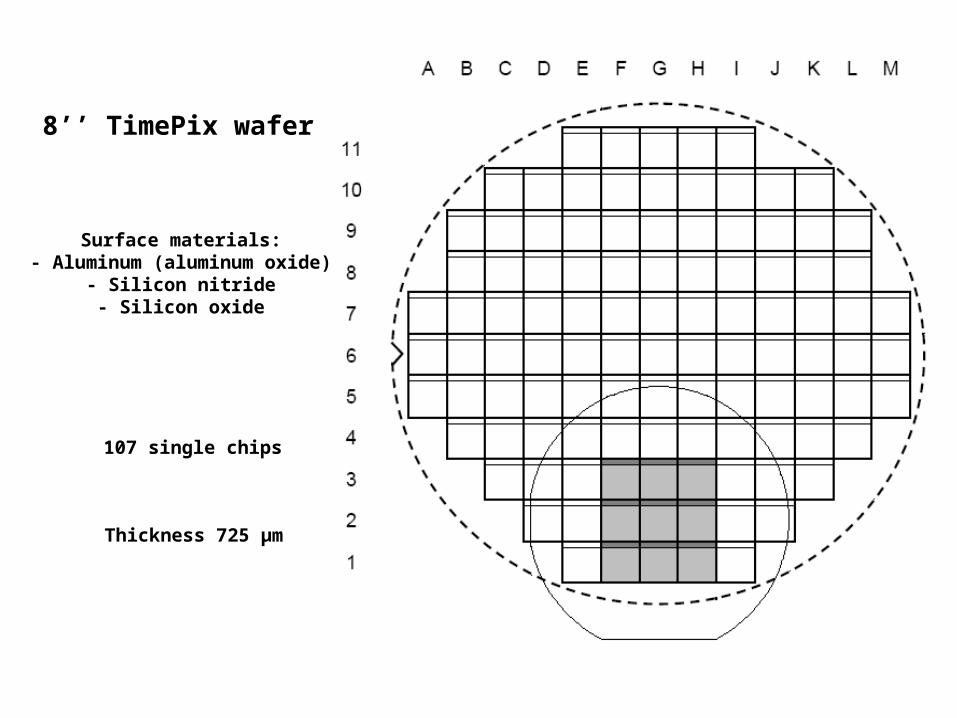
8’’ TimePix wafer
107 single chips
Thickness 725 µm
Surface materials:- Aluminum (aluminum oxide)
- Silicon nitride- Silicon oxide
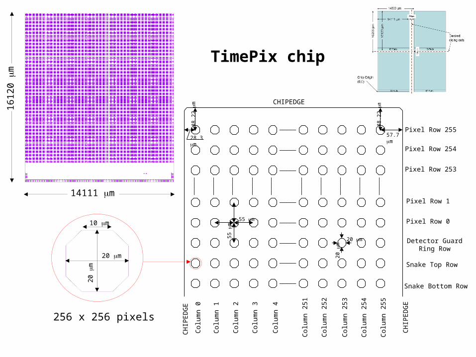
TimePix chip
14111 m
161
20
m
256 x 256 pixels
20 m
20
m
10 m
CH
IPE
DG
E
Col
umn
0
Col
umn
1
Col
umn
2
Col
umn
3
Col
umn
4
Col
umn
251
Col
umn
252
Col
umn
253
Col
umn
254
Col
umn
255
CH
IPE
DG
E
CHIPEDGE
55
m
55 m
20 m
20
m
28.3 m
48.2
2 m
48.2
2 m
57.7 m
Pixel Row 255
Pixel Row 254
Pixel Row 253
Pixel Row 1
Pixel Row 0
Detector Guard Ring Row
Snake Top Row
Snake Bottom Row

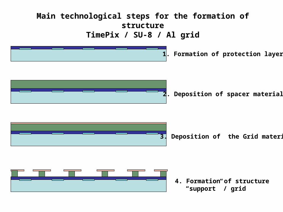
Main technological steps for the formation of structureTimePix / SU-8 / Al grid
4. Formation of structure “support” / grid
1. Formation of protection layer
2. Deposition of spacer material
3. Deposition of the Grid material

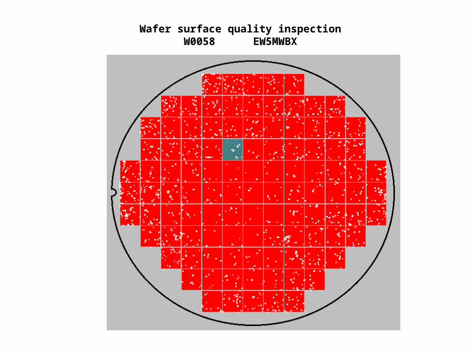
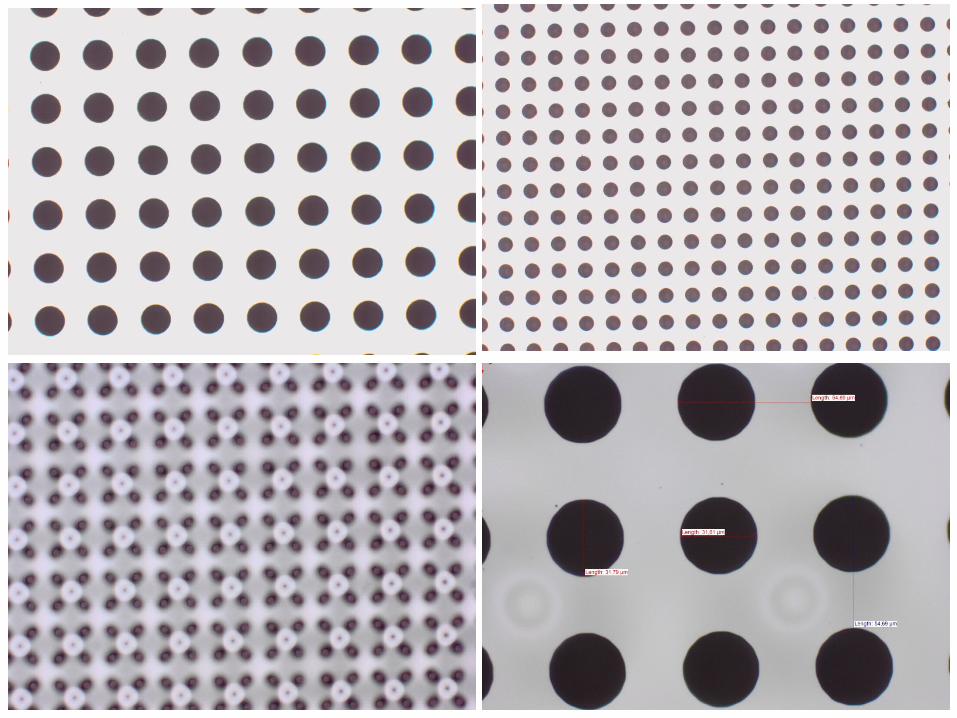
Wafer surface quality inspectionW0058 EW5MWBX
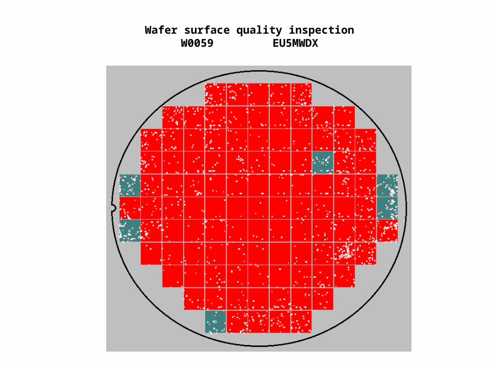
Wafer surface quality inspectionW0059 EU5MWDX
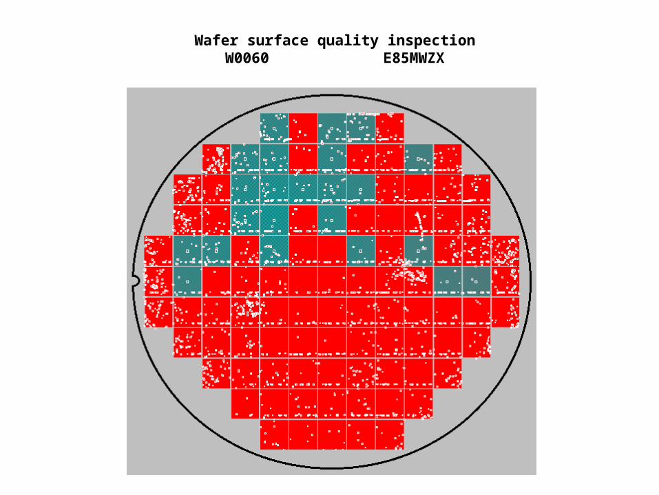
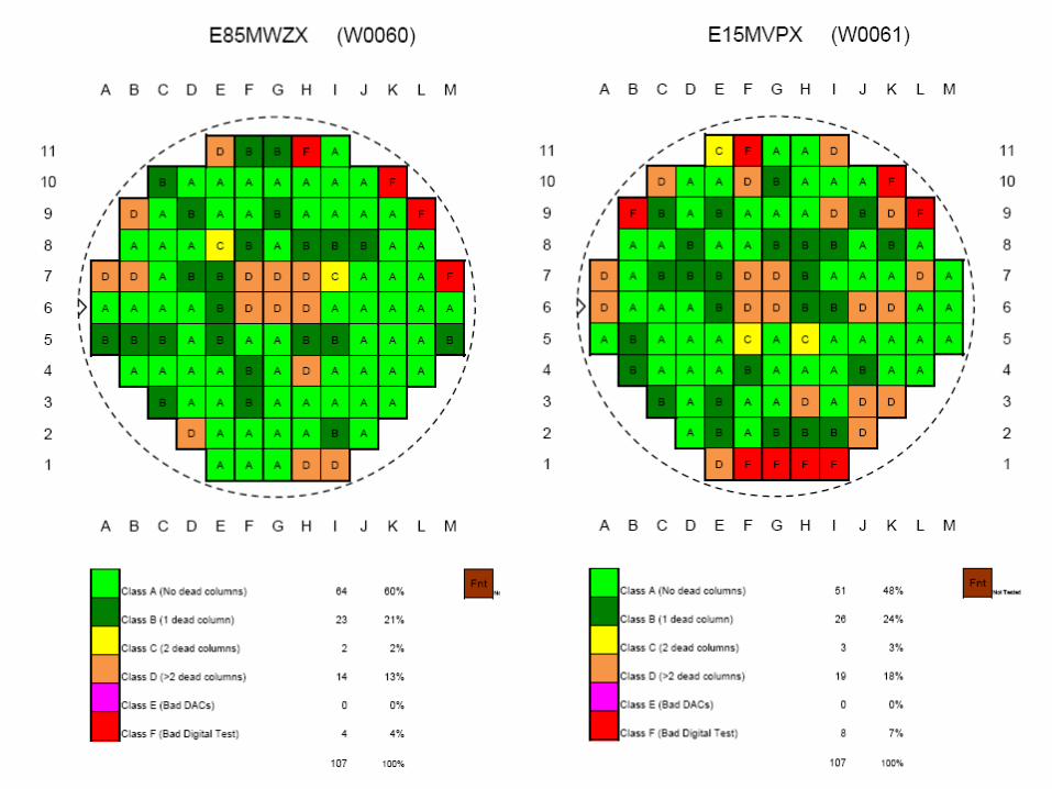
Wafer surface quality inspectionW0060 E85MWZX
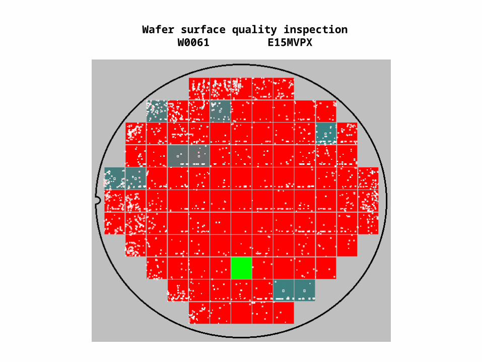
Wafer surface quality inspectionW0061 E15MVPX
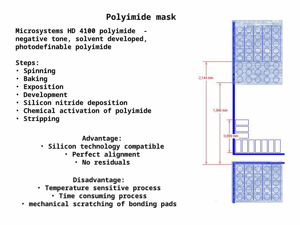
Polyimide mask
Microsystems HD 4100 polyimide - negative tone, solvent developed, photodefinable polyimide
Steps:• Spinning• Baking• Exposition• Development• Silicon nitride deposition• Chemical activation of polyimide• Stripping
Advantage:• Silicon technology compatible
• Perfect alignment• No residuals
Disadvantage:• Temperature sensitive process
• Time consuming process• mechanical scratching of bonding pads
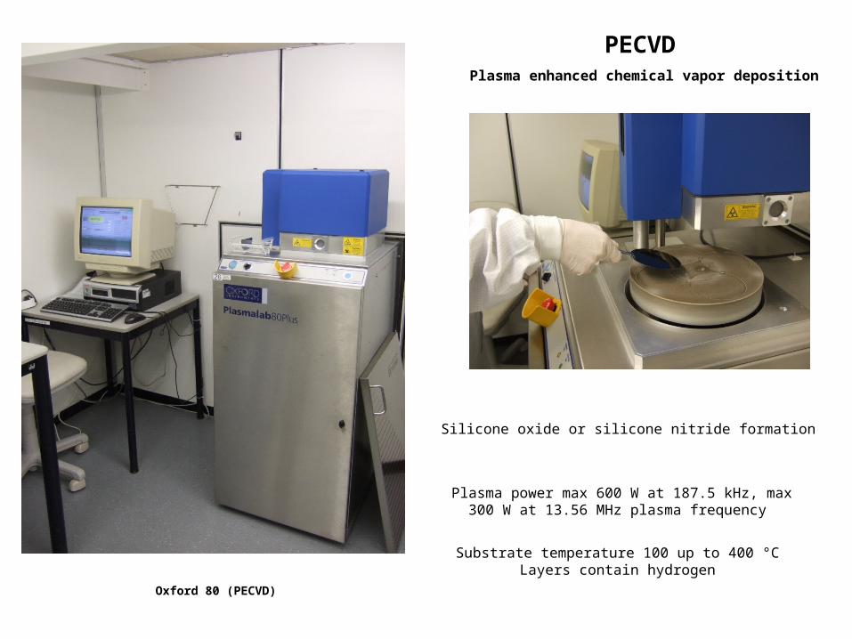
Oxford 80 (PECVD)
PECVD
Plasma enhanced chemical vapor deposition
Silicone oxide or silicone nitride formation
Plasma power max 600 W at 187.5 kHz, max 300 W at 13.56 MHz plasma frequency
Substrate temperature 100 up to 400 °C Layers contain hydrogen
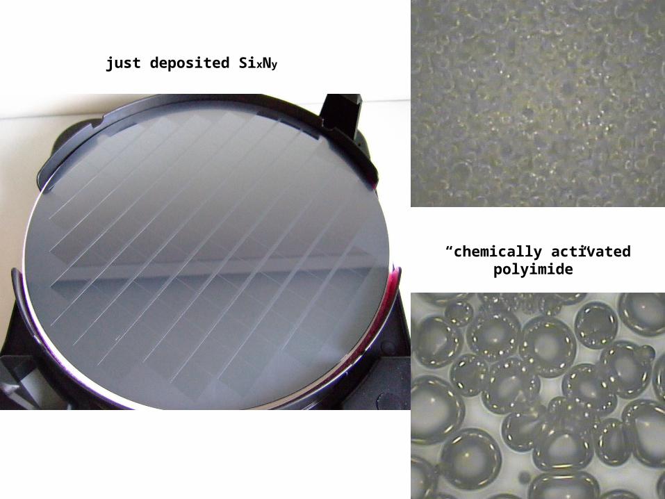
just deposited SixNy
“chemically activated polyimide”
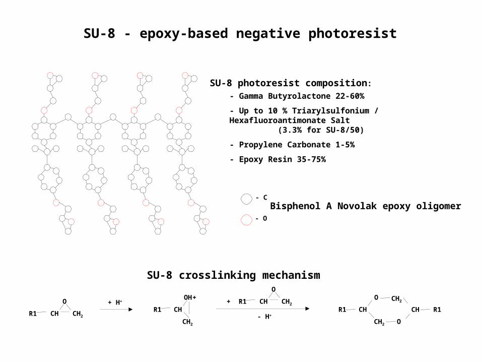
- C
- O
Bisphenol A Novolak epoxy oligomer
SU-8 photoresist composition:
- Gamma Butyrolactone 22-60%
- Up to 10 % Triarylsulfonium / Hexafluoroantimonate Salt (3.3% for SU-8/50)
- Propylene Carbonate 1-5%
- Epoxy Resin 35-75%
SU-8 - epoxy-based negative photoresist
R1
O
CH CH2
+ H+
R1
OH
CH
CH2
++ R1
O
CH CH2
- H+R1
O
CH
CH2
R1
O
CH
CH2
SU-8 crosslinking mechanism
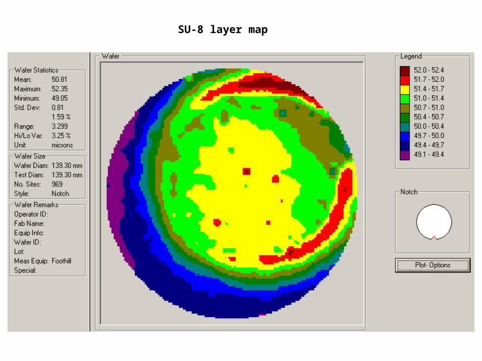
SU-8 layer map

Al layer
Sputtering system Leybold Z660
1 2 3 4 5 6 7 8 9 10 11 12 13 14 15 16 17 18 19 20 21 22 23 24 25x x x x x x x x x x x x x x x x x x x x x x
DC 50%, no sputter etching, 30 sec – the deposition time for every sputtering run, + cooling delay
Total thickness: ~ 800 nm
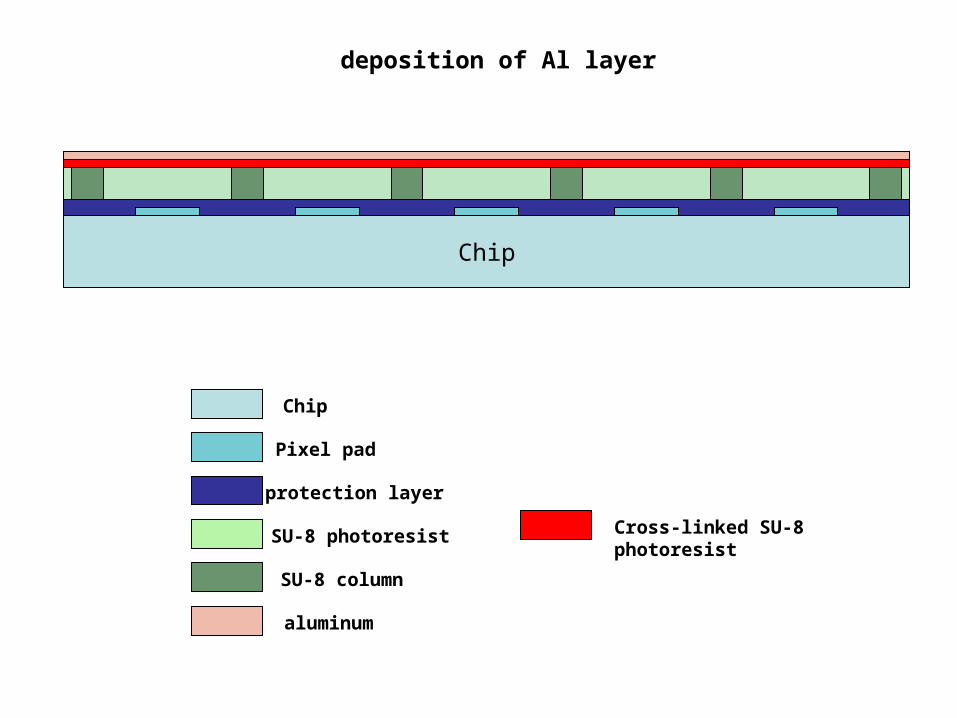
deposition of Al layer
Chip
SU-8 photoresist
aluminum
SU-8 column
protection layer
Chip
Pixel pad
Cross-linked SU-8 photoresist
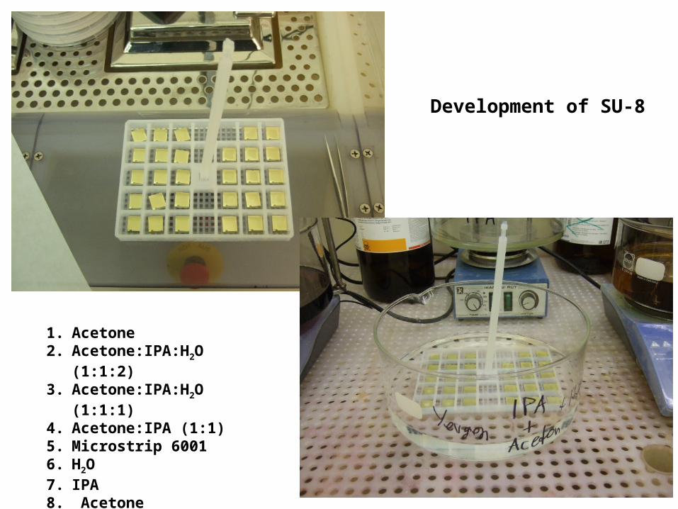
Development of SU-8
1. Acetone2. Acetone:IPA:H2O (1:1:2)3. Acetone:IPA:H2O (1:1:1)4. Acetone:IPA (1:1)5. Microstrip 60016. H2O7. IPA8. Acetone9. Drying in the air
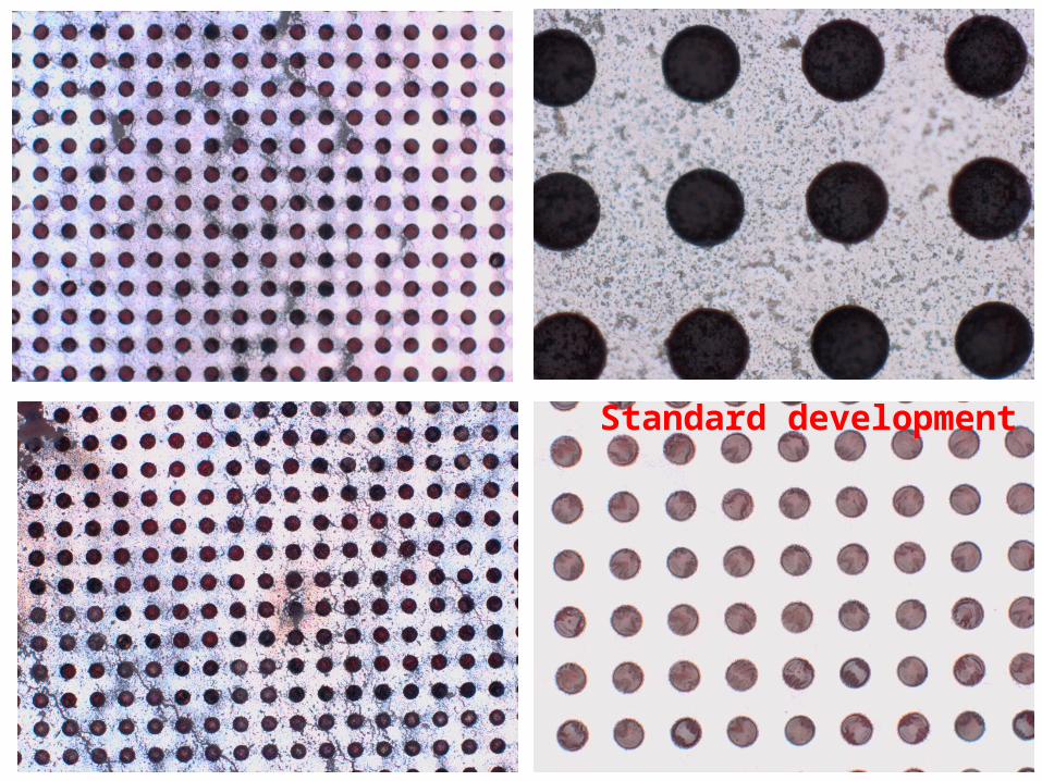
Standard development
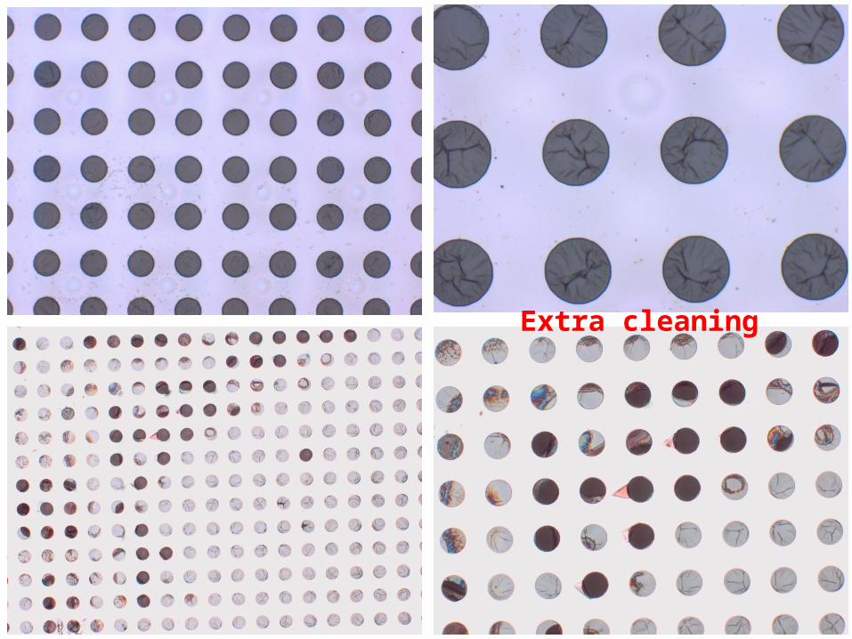
Extra cleaning

O2 plasma cleaning
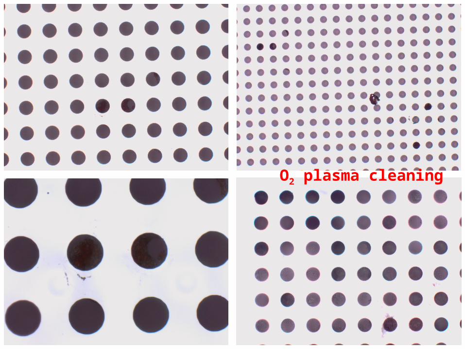
O2 plasma cleaning
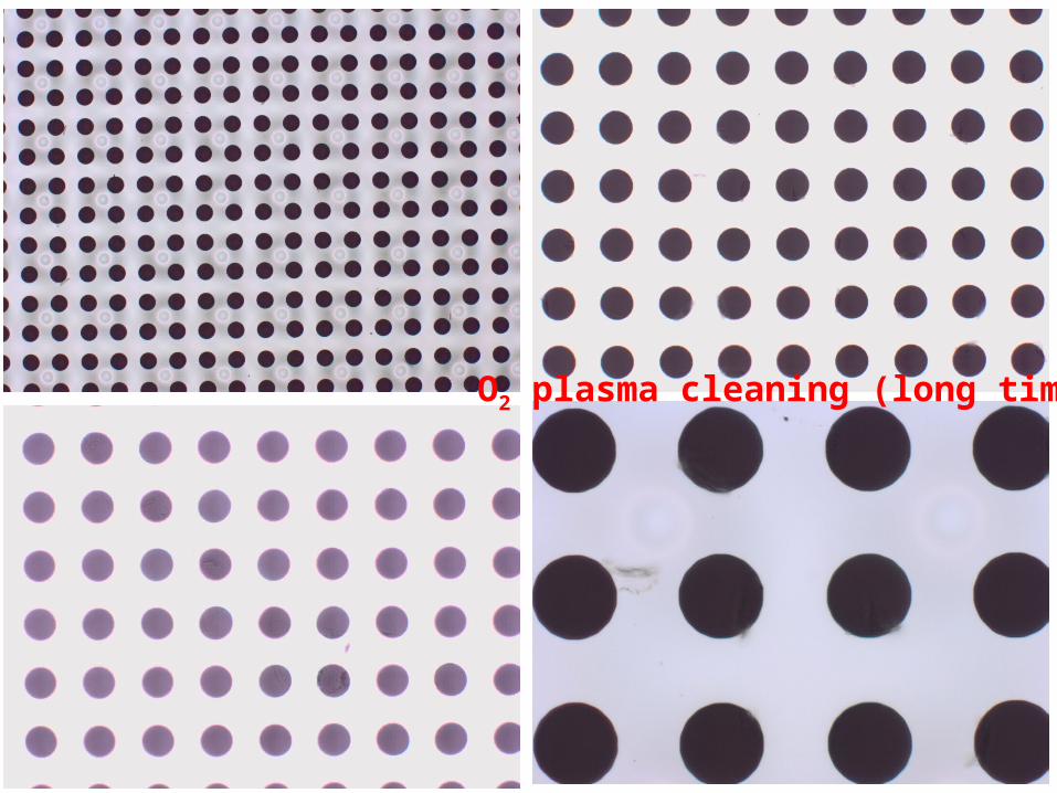
O2 plasma cleaning (long time)
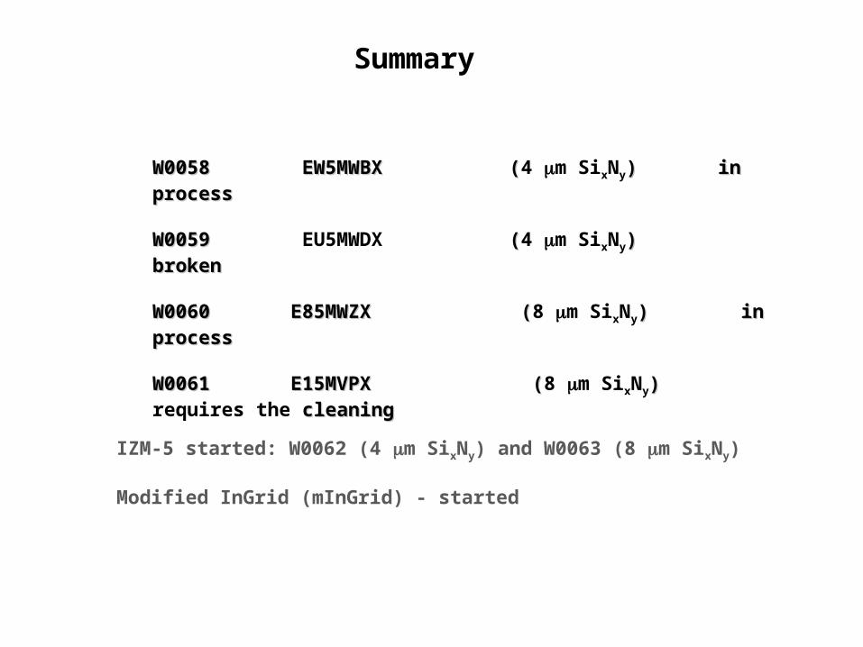
IZM-5 started: W0062 (4 m SixNy) and W0063 (8 m SixNy)
Modified InGrid (mInGrid) - started
Summary
W0058 EW5MWBX (W0058 EW5MWBX (4 m SixNy) in process) in process
W0059 W0059 EU5MWDX ( (4 m SixNy) broken) broken
W0060 E85MWZX (W0060 E85MWZX (8 m SixNy) in process) in process
W0061 E15MVPX (W0061 E15MVPX (8 m SixNy)) requires the cleaningcleaning