Embed Size (px)
Citation preview
Transistor Amplifiers
Lecture notes: Sec. 6
Sedra & Smith (6th Ed): Sec. 5.6, 5.8, 6.6 & 6.8 Sedra & Smith (5th Ed): Sec. 4.6, 4.8, 5.6 & 5.8
F. Najmabadi, ECE65, Winter 2012
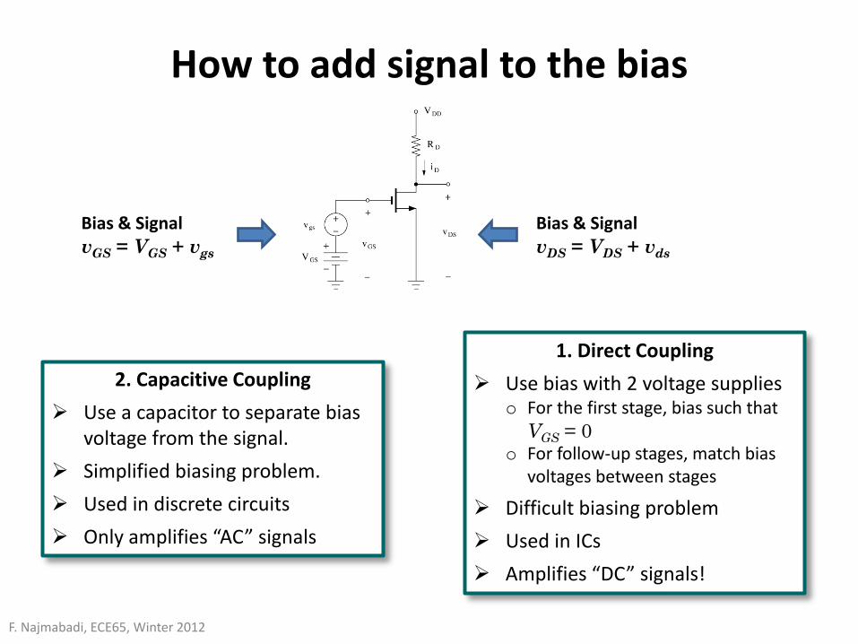
How to add signal to the bias
F. Najmabadi, ECE65, Winter 2012
Bias & Signal vGS = VGS + vgs
Bias & Signal vDS = VDS + vds
1. Direct Coupling Use bias with 2 voltage supplies
o For the first stage, bias such that VGS = 0
o For follow-up stages, match bias voltages between stages
Difficult biasing problem Used in ICs Amplifies “DC” signals!
2. Capacitive Coupling Use a capacitor to separate bias
voltage from the signal. Simplified biasing problem. Used in discrete circuits Only amplifies “AC” signals

Capacitive coupling is based on the fact that capacitors appear as open circuit in bias
F. Najmabadi, ECE65, Winter 2012
At a high enough frequency, Zc = 1/ (ωC), becomes small (effectively, capacitors become short circuit). o Mid-band parameters of an Amplifier.*
At low frequencies, Zc cannot be ignored. As Zc depends on frequency, amplifier is NOT linear (for an arbitrary signal) for these low frequencies. o Capacitors introduce a lower cut-off frequency for an amplifier (i.e., amplifier
should be operated above this frequency).
In ECE102, you will see that transistor amplifiers also have an “upper” cut-off frequency
Real Circuit Bias Circuit Signal Circuit

What are amplifier parameters?
F. Najmabadi, ECE65, Winter 2012
:Gain Voltage i
ov v
vA =
∞→
=LRi
ovo v
vA :Gain loop-Open
:ResistanceInput i
ii i
vR =
0
: Amplifier of ResistanceOutput →
=ivo
oo i
vR
Output resistance is the Thevenin resistance between the output terminals!
0
:circuit theof ResistanceOutput →
=sigvo
oout i
vR

Observations on the amplifier parameters
F. Najmabadi, ECE65, Winter 2012
Avo is the maximum possible gain of the amplifier.
Value of Ro is important. o For Ro << RL , Av ≈ Avo
o For Ro = RL , Av = 0.5 Avo o For Ro >> RL , Av ≈ 0
Prefer “small” Ro
vooL
L
i
ov A
RRR
vvA
+==
Value of Ri is important. o For Rsig << Ri , vi ≈ vsig
o For Rsig = Ri , vi = 0.5 vsig o For Rsig >> Ri , vi ≈ 0
Prefer “large” Ri
sigi
i
sig
i
RRR
vv
+=
vsigi
i
i
o
sig
i
sig
o ARR
Rvv
vv
vvA
+=×==
:Gain Overall

How to Solve Amplifier Circuits 1. Find Bias and Signal Circuits.
2. Bias circuit (signal = 0): o Capacitors are open circuit. o Use transistor large-signal model to find the bias point. o Use bias parameters to find small-signal parameters (rπ , gm , ro ).
3. Signal Circuit (IVS becomes short, ICS becomes open circuit): o Assume capacitors are short to find mid-band amplifier parameters. o Replace diodes and/or transistors with their small-signal model. o Solve for mid-band amplifier parameters (Av , Ri , Ro ).
• For most circuits, we can use fundamental amplifier configurations, elementary R forms instead of solving signal circuits.
o Include impedance of capacitors to find the lower cut-off frequency of the amplifier.
F. Najmabadi, ECE65, Winter 2012

F. Najmabadi, ECE65, Winter 2012
Example 1: Draw the small-signal equivalent of the circuit below (assume capacitors are short for small signal).
IVS → 0 R remains Caps short
Ground at the bottom
Replace MOS with its small signal model

F. Najmabadi, ECE65, Winter 2012
Example 2: Draw the small-signal equivalent of the circuit below (assume capacitors are short for small signal).
Flip PMOS
IVS → 0 Caps short Ground at the bottom
(100k || 33k = 24.8 k)
Replace MOS with its small signal model

F. Najmabadi, ECE65, Winter 2012
Example 3: Draw the small-signal equivalent of the circuit below (assume capacitors are short for small signal).
ICS → 0 (This makes ICS an open circuit)
IVS → 0 Caps short
Replace MOS with its small signal model

F. Najmabadi, ECE65, Winter 2012
Basic MOS Amplifier Configurations
We are considering only signal circuit here!
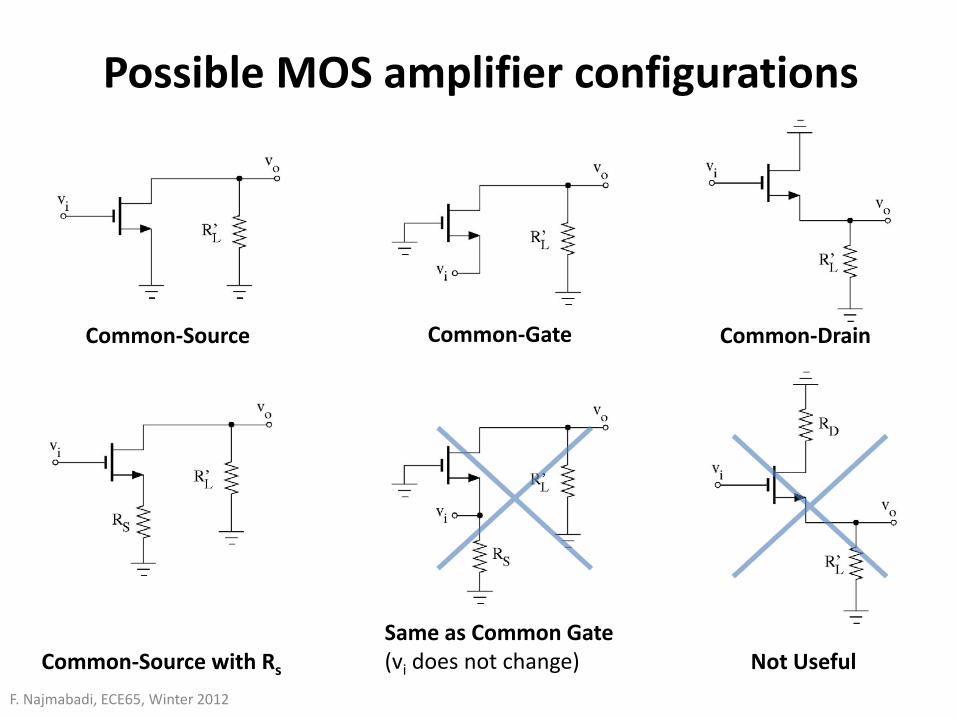
Possible MOS amplifier configurations
F. Najmabadi, ECE65, Winter 2012
Same as Common Gate (vi does not change)
Common-Source Common-Gate Common-Drain
Common-Source with Rs Not Useful
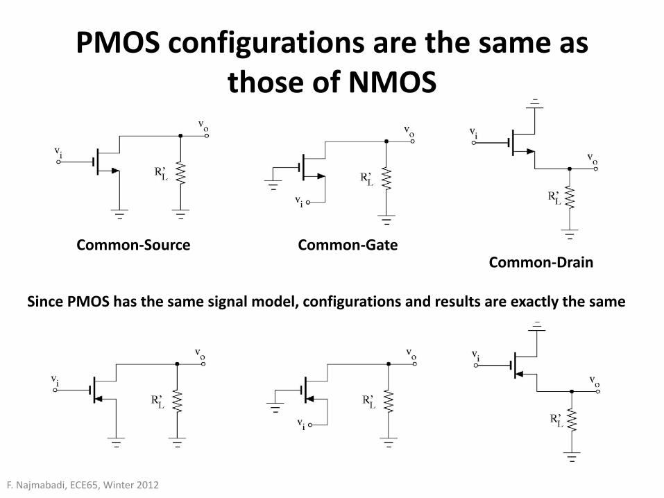
PMOS configurations are the same as those of NMOS
F. Najmabadi, ECE65, Winter 2012
Common-Source Common-Gate Common-Drain
Since PMOS has the same signal model, configurations and results are exactly the same

Common Source Configuration (Gain)
F. Najmabadi, ECE65, Winter 2012
Signal Circuit:
Signal Circuit with MOS SSM:
omvo
Lomi
ov
Logsmo
rgA
RrgvvA
Rrvgv
−=
′−==
′−=
)||(
)||(
Relevant circuit for Gain calculation
By KCL

Common Source Configuration (Ri)
F. Najmabadi, ECE65, Winter 2012
0
∞==
=
i
ii
i
ivR
i
Signal Circuit with MOS SSM:
Relevant circuit for Ri calculation

Common Source Configuration (Ro)
F. Najmabadi, ECE65, Winter 2012
oo rR = Current source becomes open circuit
Signal Circuit with MOS SSM:
Relevant circuit for Ro calculation (set vi = 0)

Common Source with Source Resistor
F. Najmabadi, ECE65, Winter 2012
0 ∞==⇒=i
iii i
vRiInput Resistance
Small Signal Circuit:
Signal Circuit with MOS SSM:

Common Source with Source Resistor (Gain)
F. Najmabadi, ECE65, Winter 2012
omvo
oLSm
Lmv
LSomo
Lom
i
ov
rgArRRg
RgA
RRrgrRrg
vvA
−=
′++′
−≈
′+++′
−==
/1
)1(
0)(
0)(
=−+−
+′
=−−−
+
−=
Simo
So
L
o
Simo
oS
S
S
Sigs
vvgr
vvRv
vvgr
vvRv
vvv
Node voltage method:
Node vS
Node vo
Relevant circuit for Gain calculation

Common Source with Source Resistor (Ro)
F. Najmabadi, ECE65, Winter 2012
)1( Somoo RrgrR ++=
Somo
x
S
S
Smo
xS
S
S
Sgs
Rrgrv
Rv
vgr
vvRv
vv
)1(
0)(
++=
=−−−
+
−=
Node voltage method:
Node vS
set vi = 0 Attach vx and compute ix
Ro = vx /ix
Somo
x
S
Sx Rrgr
vRvi
)1( ++==
Somox
x
o Rrgrvi
R )1(11++
=≡

Common Gate Configuration
F. Najmabadi, ECE65, Winter 2012
omvo
Lomv
Loo
om
i
ov
rgARrgA
Rrr
rgvvA
≈
′≈
′+==
)||(
)||(1
io
om
Lo
o
imo
io
L
o
igs
vr
rgRr
v
vgr
vvRv
vv
+=
′
=−+−
+′
−=
1||
0)(
Node voltage method:
Node vo
Gain

Common Gate Configuration (Ri and Ro)
F. Najmabadi, ECE65, Winter 2012
om
L
mi
om
Lo
i
ii
rgR
gR
rgRr
ivR
′+≈
+′+
==
1
1
)()1(
)(
Loiomi
Liogsmii
RrirgvRirvgiv′+=+
′++=KVL:
oo rR =
Current source becomes open circuit
Output Resistance (set vi = 0)
Input Resistance

Common Drain Configuration (Source Follower)
F. Najmabadi, ECE65, Winter 2012
11
)||(1
)||(
≈+
=
′+′
=
om
omvo
Lom
Lomv
rgrgA
RrgRrgA
omLo
oim
oimo
o
L
o
oigs
vgRr
vvg
vvgrv
Rv
vvv
+′
=
=−−+′
−=
||
0)(
Node voltage method:
Node vo
Gain
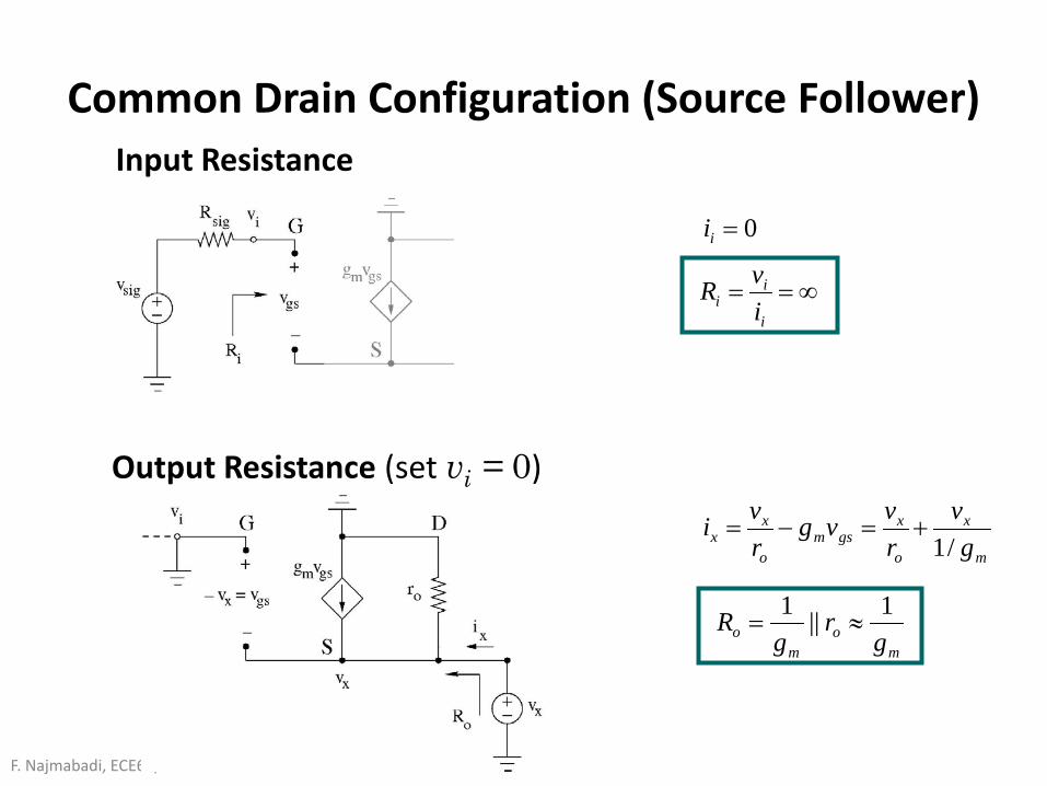
Common Drain Configuration (Source Follower)
F. Najmabadi, ECE65, Winter 2012
m
x
o
xgsm
o
xx g
vrvvg
rvi
/1+=−=
Input Resistance
Output Resistance (set vi = 0)
1||1 m
om
o gr
gR ≈=
0=ii
∞==i
ii i
vR

MOS Basic Amplifier Configurations (PMOS circuits are identical)
F. Najmabadi, ECE65, Winter 2012
Common Source with RS oLSm
Lmv rRRg
RgA/1 ′++
′−=
Common Drain/Source Follower
)||(1)||(
Lom
Lomv Rrg
RrgA′+
′=
Common Source )||( Lomv RrgA ′−=
Common Gate )||( Lomv RrgA ′=

MOS Elementary R forms

A Transistor can be configured to act as a resistor for small signals!
F. Najmabadi, ECE65, Winter 2012
oo rR =Set vi = 0, current source becomes open circuit
Ex: Output resistance of a CS Amplifier
or
If we connect any two terminals of a MOS, we get a two-terminal device. o For Small Signals, this two terminal device can be replaced with its
Thevenin equivalent circuit. o As there is NO independent sources present, the Thevenin
equivalent circuit is reduced to a resistor.
Notation: ro is the small-signal resistance between the point and ground

Transistor can be configured to act as a resistor for small signals!
F. Najmabadi, ECE65, Winter 2012
But, MOS should be in saturation for small signal model to work! o Connection between MOS terminals are, therefore, made through
ground for small signals. o In fact, one or both MOS terminals have to be connected to bias power
supplies to ensure that MOS is in saturation
Small Signal Circuit Real Circuit
A)
No Small Signal circuit MOS is NOT in saturation
B)

MOS Elementary R forms (PMOS circuits are identical)
F. Najmabadi, ECE65, Winter 2012
∞
Input resistance of CS Amp
Output resistance of CS Amp with Rs
)1()1(Rgr
RRgr
mo
mo
+≈++
Input resistance of CG Amp
om
o
rgRr
++
1
Diode-connected Transistor Always in saturation! m
om g
rg
1||1≈
Above configurations are for Small Signal. Typically one or both “signal” grounds are actually connected to bias voltage sources to ensure that MOS is in saturation!
or
F. Najmabadi, ECE65, Winter 2012
Basic BJT Amplifier Configurations
We are considering only signal circuit here!
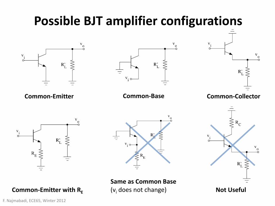
Possible BJT amplifier configurations
F. Najmabadi, ECE65, Winter 2012
Same as Common Base (vi does not change)
Common-Emitter Common-Base Common-Collector
Common-Emitter with RE Not Useful
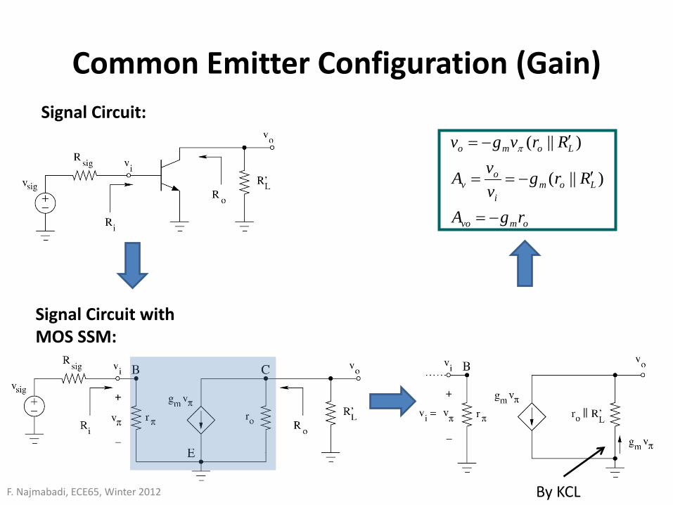
Common Emitter Configuration (Gain)
F. Najmabadi, ECE65, Winter 2012
Signal Circuit:
Signal Circuit with MOS SSM:
omvo
Lomi
ov
Lomo
rgA
RrgvvA
Rrvgv
−=
′−==
′−=
)||(
)||( π
By KCL
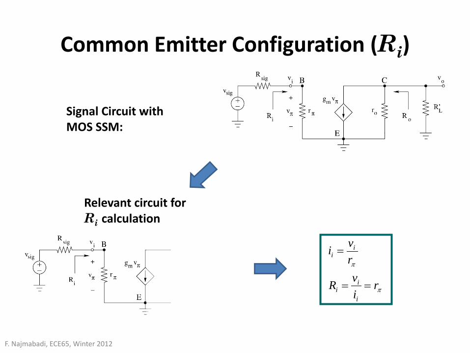
Common Emitter Configuration (Ri)
F. Najmabadi, ECE65, Winter 2012
π
π
rivR
rvi
i
ii
ii
==
=
Signal Circuit with MOS SSM:
Relevant circuit for Ri calculation
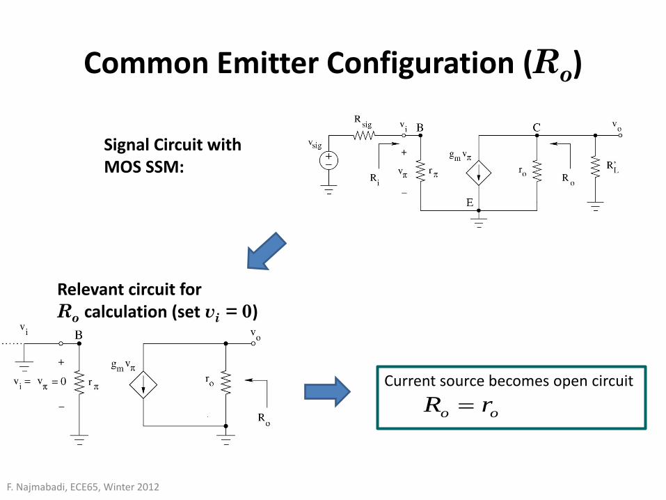
Common Emitter Configuration (Ro)
F. Najmabadi, ECE65, Winter 2012
oo rR = Current source becomes open circuit
Signal Circuit with MOS SSM:
Relevant circuit for Ro calculation (set vi = 0)

BJT Basic Amplifier Configurations (PNP circuits are identical)
F. Najmabadi, ECE65, Winter 2012
Common Emitter with RE
Common Collector/ Emitter Follower
)||(1)||(
Lom
Lomv Rrg
RrgA′+
′=
Common Emitter )||( Lomv RrgA ′−=
Common Base )||( Lomv RrgA ′=
)/1)(/(1 πrRrRRgRgA
EoLEm
Lmv +′++
′−=

BJT Elementary R forms (PNP circuits are identical)
F. Najmabadi, ECE65, Winter 2012
om
o
rgRr
++
≈1
or
)1( Rgr mo +≈
βπ Rr +
≈Rr )1( βπ ++

F. Najmabadi, ECE65, Winter 2012
Discrete Amplifier Configurations
We focus on biasing with Emitter/Source degeneration!

Emitter-degeneration bias circuits
F. Najmabadi, ECE65, Winter 2012
Bias with one power supply
(voltage divider)
EEBEBBBB RIVRIV ++=
Bias with two power supplies
EEBEBBEE RIVRIV ++=

Emitter-degeneration bias circuits have similar signal circuits
F. Najmabadi, ECE65, Winter 2012
Bias with one power supply (voltage divider)
Bias with two power supplies
The same circuit for
21 || BBB RRR =
Signal Circuits
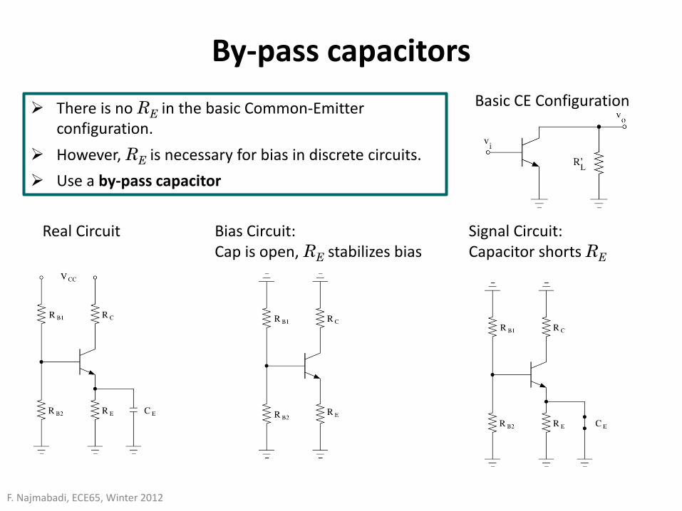
By-pass capacitors
F. Najmabadi, ECE65, Winter 2012
Basic CE Configuration There is no RE in the basic Common-Emitter configuration.
However, RE is necessary for bias in discrete circuits. Use a by-pass capacitor
Real Circuit Bias Circuit: Cap is open, RE stabilizes bias
Signal Circuit: Capacitor shorts RE

Discrete Common-Emitter Amplifier
F. Najmabadi, ECE65, Winter 2012
Standard Bias Circuit:* Caps are open circuit
Real Circuit
CE amplifier: Input at the base Output at the collector
* Bias calculations are NOT done here as we have done them before.

Signal circuit of the discrete CE Amplifier
F. Najmabadi, ECE65, Winter 2012
Real Circuit
Short caps Zero bias supplies
Rearrange

Discrete CE Amplifier (Gain)
F. Najmabadi, ECE65, Winter 2012
i
o
sigi
i
sig
o
LComi
o
vv
RRR
vv
RRrgvv
×+
=
−=
)||||(
Basic CE configuration
Signal input at the base Signal output at the collector No RE LCL RRR ||=′

Discrete CE Amplifier (Ri)
F. Najmabadi, ECE65, Winter 2012
Replace transistor with its equivalent resistance
Elementary R form
|| πrRR Bi =
πrR =
πrR =

Discrete CE Amplifier (Ro)
F. Najmabadi, ECE65, Winter 2012
Set vsig = 0 Replace transistor with its equivalent resistance
Elementary R form
|| oCo rRR =
orR =

Discrete CE and CS Amplifiers
F. Najmabadi, ECE65, Winter 2012
||
)||||(
oDo
Gi
LDomi
o
rRRRR
RRrgvv
==
−=
i
o
sigi
i
sig
o
vv
RRR
vv
×+
=
|| ||
)||||(
oCo
Bi
LComi
o
rRRrRR
RRrgvv
==
−=
π

Discrete CS Amplifier with RS
F. Najmabadi, ECE65, Winter 2012
Real Circuit
Signal Circuit Short caps Zero bias supplies
CS amplifier with RS Input at the gate Output at the drain
Bias Circuit Caps open

Discrete CS Amplifier with RS (Gain)
F. Najmabadi, ECE65, Winter 2012
i
o
sigi
i
sig
o
oLDSm
LDm
i
o
vv
RRR
vv
rRRRgRRg
vv
×+
=
++−=
/)||( 1
)||(
Basic CS configuration with RS
LDL RRR ||=′
Signal input at the gate Signal output at the drain RS !

Discrete CS Amplifier with RS (Ri)
F. Najmabadi, ECE65, Winter 2012
Gi RR =
Replace transistor with its equivalent resistance
Elementary R form
∞= R
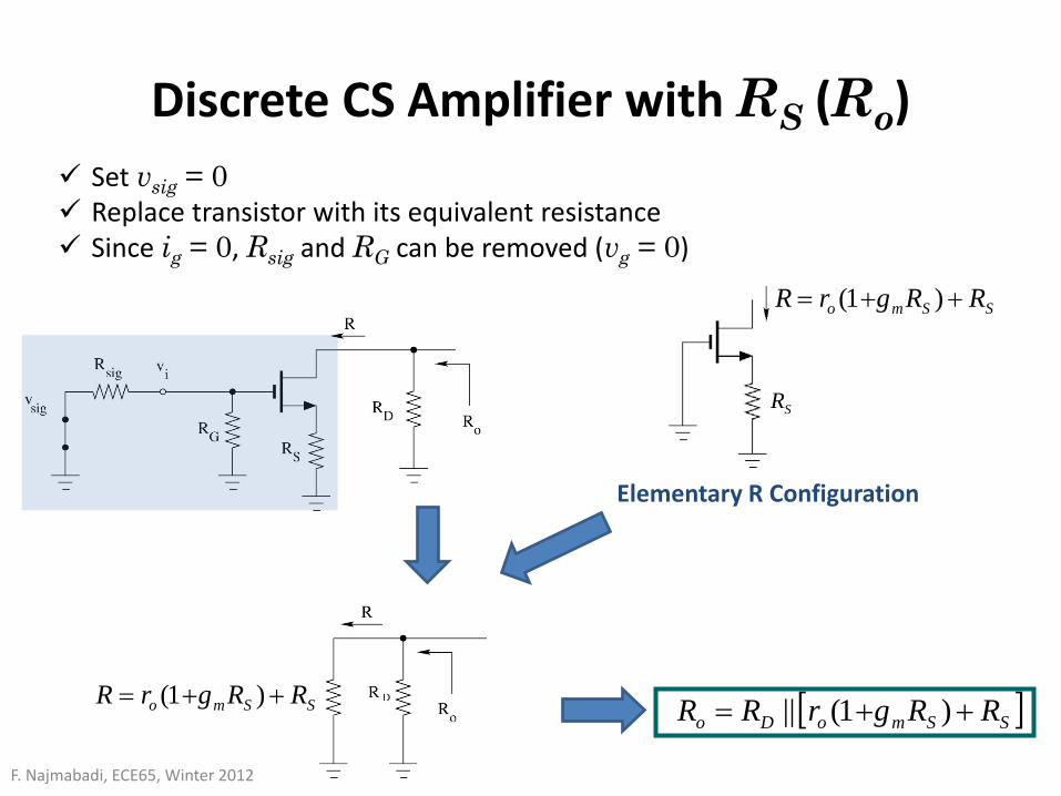
Discrete CS Amplifier with RS (Ro)
F. Najmabadi, ECE65, Winter 2012
[ ] )1( || SSmoDo RRgrRR ++=
Set vsig = 0 Replace transistor with its equivalent resistance Since ig = 0, Rsig and RG can be removed (vg = 0)
Elementary R Configuration
SSmo RRgrR ++= )1(
SR
SSmo RRgrR ++= )1(

Discrete CE and CS Amplifiers with RE / RS
F. Najmabadi, ECE65, Winter 2012
[ ] )1( ||
/)||( 1
)||(
SSmoDo
Gi
oLDSm
LDm
i
o
RRgrRRRR
rRRRgRRg
vv
++==
++−=
i
o
sigi
i
sig
o
vv
RRR
vv
×+
=
[ ]
+++≈
++≈+
−≈
+++−=
sigBE
EoCo
EBi
Em
LDm
i
o
EoLDEm
LDm
i
o
RRRrRrRR
RrRRRgRRg
vv
rRrRRRgRRg
vv
||1 ||
)1( || 1
)||(
)/1](/)||[(1)||(
π
π
π
β
β
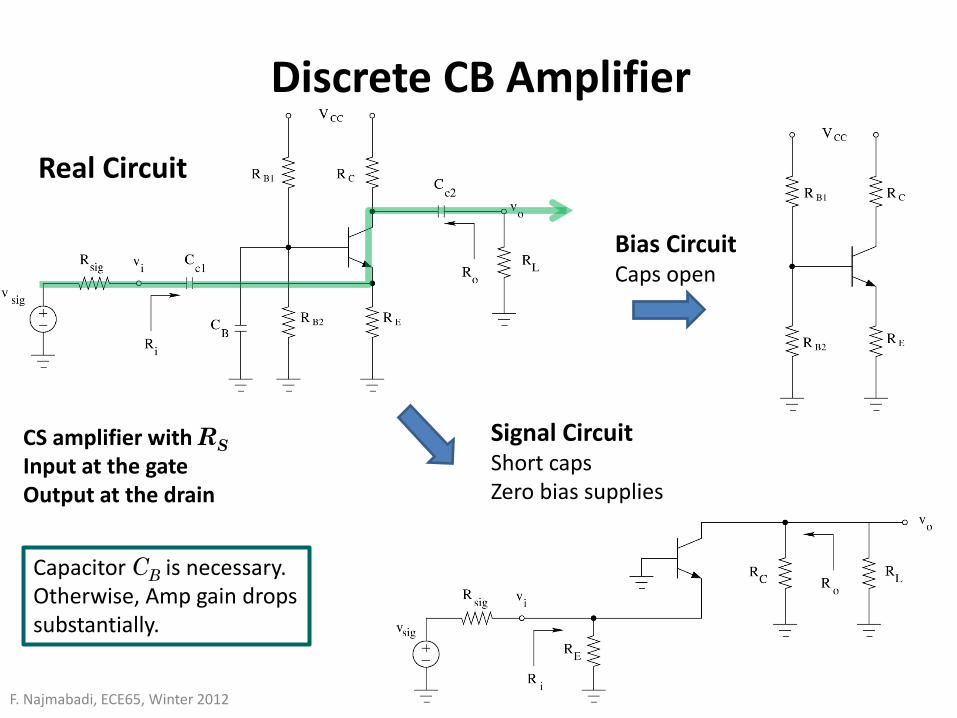
Discrete CB Amplifier
F. Najmabadi, ECE65, Winter 2012
Real Circuit
Signal Circuit Short caps Zero bias supplies
CS amplifier with RS Input at the gate Output at the drain
Bias Circuit Caps open
Capacitor CB is necessary. Otherwise, Amp gain drops substantially.

Discrete CB Amplifier (Gain)
Basic CB form
LCL RRR ||=′
Signal input at the source Signal output at the drain
i
o
sigi
i
sig
o
LComi
o
vv
RRR
vv
RRrgvv
×+
=
+=
)||||(

om
LCo
rgRRrR
++
=1
)||(
Discrete CB Amplifier (Ri)
1
)||( ||
+
+=
om
LCoEi rg
RRrRR
Replace transistor with its equivalent resistance
Elementary R Configuration
LC RR ||
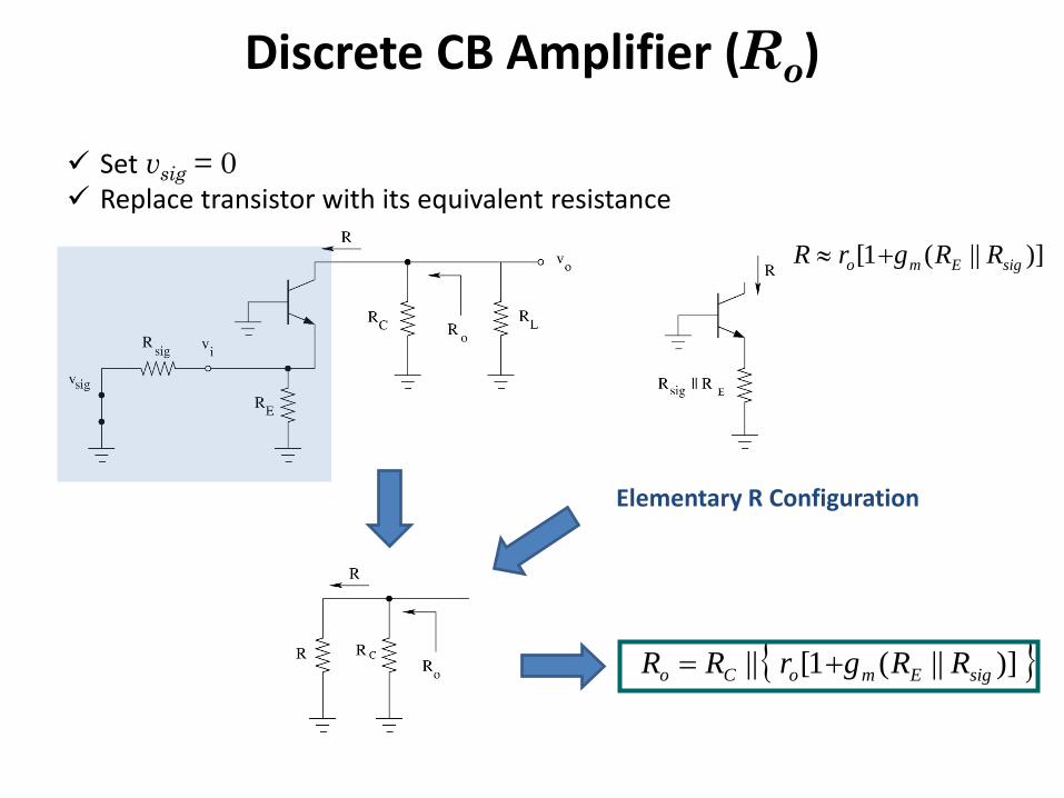
Discrete CB Amplifier (Ro)
{ } )]||(1[ || sigEmoCo RRgrRR +=
Set vsig = 0 Replace transistor with its equivalent resistance
Elementary R Configuration
)]||(1[ sigEmo RRgrR +≈

Discrete CB and CG Amplifiers
F. Najmabadi, ECE65, Winter 2012 i
o
sigi
i
sig
o
vv
RRR
vv
×+
=
{ } )]||(1[ || 1
)||( ||
)||||(
sigEmoCo
om
LCoEi
LComi
o
RRgrRRrgRRrRR
RRrgvv
+=
+
+=
+=
{ } )]||(1[ || 1
)||( ||
)||||(
sigSmoDo
om
LDoSi
LDomi
o
RRgrRRrgRRrRR
RRrgvv
+=
+
+=
+=

Discrete CD Amplifier (Source Follower)
F. Najmabadi, ECE65, Winter 2012
Real Circuit
Signal Circuit Short caps Zero bias supplies
CS amplifier with RS Input at the gate Output at the drain
Bias Circuit Caps open

Discrete CD Amplifier (Gain)
F. Najmabadi, ECE65, Winter 2012
Basic CD form
Signal input at the gate Signal output at the source
i
o
sigi
i
sig
o
LSom
LSom
i
o
vv
RRR
vv
RRrgRRrg
vv
×+
=
+=
)||||(1
)||||(
LSL RRR ||=′

Discrete CD Amplifier (Ri)
F. Najmabadi, ECE65, Winter 2012
Replace transistor with its equivalent resistance
Elementary R Configuration
∞
Gi RR =

Discrete CD Amplifier (Ro)
F. Najmabadi, ECE65, Winter 2012
1 || m
So gRR =
R
Elementary R Configuration
Set vsig = 0 Replace transistor with its equivalent resistance Since ig = 0, Rsig and RG can be removed (vg = 0)
Rm
om g
rg
1||1≈
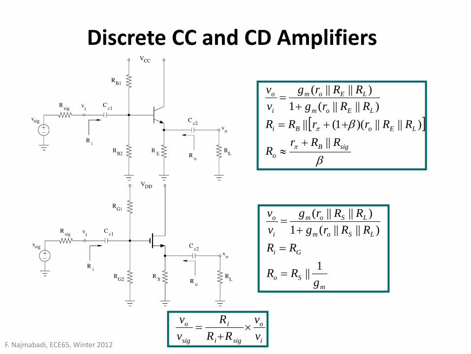
Discrete CC and CD Amplifiers
F. Najmabadi, ECE65, Winter 2012
1 ||
)||||(1
)||||(
mSo
Gi
LSom
LSom
i
o
gRR
RRRRrg
RRrgvv
=
=+
=
i
o
sigi
i
sig
o
vv
RRR
vv
×+
=
[ ]
β
β
π
π
sigBo
LEoBi
LEom
LEom
i
o
RRrR
RRrrRRRRrg
RRrgvv
||
)||||)(1( || )||||(1
)||||(
+≈
++=+
=
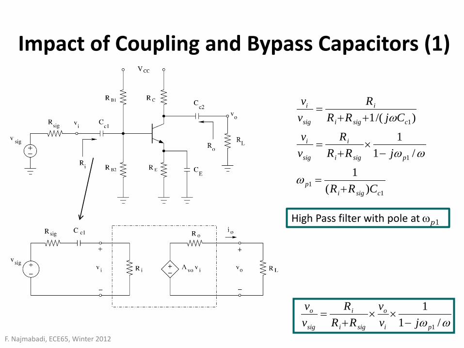
Impact of Coupling and Bypass Capacitors (1)
F. Najmabadi, ECE65, Winter 2012
11
1
1
)(1
/11
)/(1
csigip
psigi
i
sig
i
csigi
i
sig
i
CRR
jRRR
vv
CjRRR
vv
+=
−×
+=
++=
ω
ωω
ω
High Pass filter with pole at ωp1
ωω /11
1pi
o
sigi
i
sig
o
jvv
RRR
vv
−××
+=

Impact of Coupling and Bypass Capacitors (2)
F. Najmabadi, ECE65, Winter 2012
Each capacitor introduces a pole!
Poles can be found by inspection: 1) Set vsig = 0 2) Consider each capacitor separately
(i.e., assume all others are short). 3) Find R, the total resistance seen
between capacitor terminals 4) Pole is given by
1 21
cp CR
fπ
=
The lower cut-off frequency of amplifiers can be found from ... 21 ++≈ ppp fff