Electronics Engineering Operational Amplifiers and Applications
1 Mr. Amod Kumar , Dept. of ECE, Faculty of Engineering & Technology, KMCUAF University, Lucknow
Unit-5
Operational Amplifiers and Applications Syllabus: Operational Amplifiers Concept of ideal operational amplifiers, ideal op-amp parameters, inverting, non- inverting and unity gain amplifiers, adders.
( 4Hours)
Introduction
An operational amplifier, or op-amp, is the most important and versatile analog IC. It is a
direct coupled multistage voltage amplifier with an extremely high gain. With the help of op-
amp, the circuit design becomes very simple. The variety of useful circuits can be built without
the necessity of knowing about the complex internal circuitry.
Fig. 1 shows circuit symbol and circuit model of an op-amp.
Fig. 1 Circuit symbol and model of an op-amp
An op-amp has two input terminals – an inverting input 𝑉1 and a non-inverting input 𝑉2,
and an output 𝑉𝑜. It requires two power supplies: +𝑉𝐶𝐶 and −𝑉𝐸𝐸. It has a very high input
impedance 𝑍𝑖𝑛, a very low output impedance 𝑍𝑜𝑢𝑡 and a very high gain 𝐴.
Advantages of Op-Amps
Low cost
Small size
Versatility
Flexibility
Dependability
Applications of Op-Amps
Op-amps have become an integral part of almost every electronic circuit which uses
linear integrated circuits.
Op-amps are used in analog signal processing and analog filtering.
They are used to perform mathematical operations such as addition, subtraction,
multiplication, integration, differentiation, etc.

2
Mr. Amod Kumar , Dept. of ECE, Faculty of Engineering & Technology, KMCUAF University, Lucknow
They are used in the fields of process control, communications, computers, power and
signal sources, displays and measuring systems.
They are used in linear applications like voltage follower, differential amplifier, inverting
amplifier, non-inverting amplifier, etc. and non-linear applications like precision
rectifiers, comparators, clampers, Schmitt trigger circuit, etc.
Ideal Op-Amp
Fig. 2 gives the representation of ideal and practical op-amps.
Fig. 2 Representation of ideal and practical op-amps
An ideal op-amp has the following characteristics:
1. Infinite voltage gain (𝑨𝒐𝒍 = ∞): The voltage gain, also known as differential open loop
gain is infinite in an ideal op-amp.
2. Infinite input impedance (𝒁𝒊𝒏 = ∞): The input impedance is infinite in an ideal op-amp.
This means that no current can flow into an ideal op-amp.
3. Zero output impedance (𝒁𝒐𝒖𝒕 = 𝟎): The output impedance is zero in an ideal op-amp.
This means that the output voltage remains the same, irrespective of the value of the load
connected.
4. Zero offset voltage (𝑽𝑶𝑺 = 𝟎): The presence of the small output voltage even when 𝑉1 =
𝑉2 = 0 is called offset voltage. In an ideal op-amp, offset voltage is zero. This means the
output is zero if the input is zero.
5. Infinite bandwidth (𝑩𝑾 = ∞): The range of frequencies over which the amplifier
performance is satisfactory is called its bandwidth. The bandwidth of an ideal op-amp is
infinite.
6. Infinite CMRR (𝑪𝑴𝑹𝑹 = ∞): The ratio of differential gain to common mode gain is
called common mode rejection ratio (CMRR). In an ideal op-amp, CMRR is infinite. This
means that the common mode gain is zero in an ideal op-amp.
7. Infinite slew rate (𝑺 = ∞): Slew rate is the maximum rate of change of output voltage
with time. In an ideal op-amp, slew rate is infinite. This means that the changes in the
output voltage occur simultaneously with the changes in the input voltage.

Electronics Engineering Operational Amplifiers and Applications
3 Mr. Amod Kumar , Dept. of ECE, Faculty of Engineering & Technology, KMCUAF University, Lucknow
Unit-5
8. No effect of temperature: The characteristics of an ideal op-amp do not change with the
changes in temperature.
9. Zero PSRR (𝑷𝑺𝑹𝑹 = 𝟎): Power supply rejection ratio (PSRR) is defined as the ratio of
the change in input offset voltage due to the change in supply voltage producing it,
keeping other power supply voltage constant. In an ideal op-amp, PSRR is zero.
Practical Op-Amp
Characteristics of a practical op-amp are very high voltage gain, very high input
impedance, and very low output impedance.
Internal Block Diagram of an Op-Amp
A typical op-amp is made up of three types of amplifier circuits: a differential amplifier, a
voltage amplifier, and a push-pull amplifier, as shown in Fig. 3.
Fig. 3 Basic internal arrangement of an op-amp
The differential amplifier is the input stage for the op-amp. It provides amplification of
the difference voltage between the two inputs.
The second stage is usually a class A amplifier that provides additional gain. Some op-
amps may have more than one voltage amplifier stage.
A push-pull class B amplifier is typically used for the output stage.
Op-Amp IC 741
IC 741is the most popular IC version of op-amp. It is an 8-pin IC as shown in Fig. 4.
Fig. 4 Pin diagram of IC 741
Pin 2 is the inverting input terminal and Pin 3 is the non-inverting input terminal

4
Mr. Amod Kumar , Dept. of ECE, Faculty of Engineering & Technology, KMCUAF University, Lucknow
Pin 6 is the output terminal
Pin 4 is for −𝑉𝐸𝐸 (𝑉−) supply and pin 7 is for +𝑉𝐶𝐶 (𝑉+) supply
Pins 1 and 5 are offset null pins. These are used to nullify offset voltage
Pin 8 is a dummy pin and no connection is made to this pin
Op-Amp Input Modes
The input signal modes are determined by the differential amplifier input stage of the op-
amp.
Differential Mode
In the differential mode, either one signal is applied to an input with the other input
grounded or two opposite-polarity signals are applied to the inputs.
Single-Ended Differential Mode
When an op-amp is operated in the single-ended differential mode, one input is grounded
and a signal voltage is applied to the other input, as shown in Fig. 5.
Fig. 5 Single-ended differential mode
In the case where the signal voltage is applied to the inverting input as in Fig. 5 (a), an
inverted, amplified signal voltage appears at the output. In the case where the signal is applied
to the noninverting input with the inverting input grounded, as in Fig. 5(b), a noninverted,
amplified signal voltage appears at the output.
Double-Ended Differential Mode
In the double-ended differential mode, two opposite-polarity (out-of-phase) signals are
applied to the inputs, as shown in Fig. 6(a). The amplified difference between the two inputs
appears on the output.
Fig. 6 Double-ended differential mode

Electronics Engineering Operational Amplifiers and Applications
5 Mr. Amod Kumar , Dept. of ECE, Faculty of Engineering & Technology, KMCUAF University, Lucknow
Unit-5
Equivalently, the double-ended differential mode can be represented by a single source
connected between the two inputs, as shown in Fig. 6(b).
Common Mode
In the common mode, two signal voltages of the same phase, frequency, and amplitude
are applied to the two inputs, as shown in Fig. 7.
Fig. 7 Common mode operation
When equal input signals are applied to both inputs, they tend to cancel, resulting in a
zero output voltage. This action is called common-mode rejection. Its importance lies in the
situation where an unwanted signal appears commonly on both op-amp inputs. Common-mode
rejection means that this unwanted signal will not appear on the output and distort the desired
signal.
Op-Amp Parameters
Open-Loop Voltage Gain (Differential Gain)
An op-amp amplifies the difference between the two input signals 𝑽𝒅 = 𝑽𝟐 − 𝑽𝟏. The
output voltage is given by
where Aol
𝑽𝒐 = 𝑨𝒐𝒍𝑽𝒅 = 𝑨𝒐𝒍(𝑽𝟐 − 𝑽𝟏)
is the open-loop voltage gain, also called differential gain given by 𝑨𝒐𝒍
=
𝑽𝒐
𝑽𝒅
The open-loop voltage gain of an op-amp is the internal voltage gain of the device and
represents the ratio of output voltage to input voltage when there are no external components.
Generally 𝐴 is expressed in decibel (dB) as 𝑨 = 𝟐𝟎 𝒍𝒐𝒈 𝑽𝒐 .
𝑜𝑙
Common Mode Gain
𝒐𝒍 𝟏𝟎 ( 𝑽𝒅
) 𝒅𝑩
If we apply two input voltages which are equal i.e. if 𝑉1 = 𝑉2, then ideally the output must
be zero. But practically, the output voltage not only depends on the difference voltage but also
depends on the average common level of the two inputs. Such a common level is called common
mode signal 𝑽𝒄 = 𝑽𝟏+𝑽𝟐.
𝟐
The differential amplifier produces the output voltage proportional to common mode
signal and the output voltage is given as
where 𝐴𝑐𝑚
𝑽𝒐 = 𝑨𝒄𝒎𝑽𝒄
is the common mode gain given by 𝑨𝒄𝒎
=
𝑽𝒐
𝑽𝒄

6
Mr. Amod Kumar , Dept. of ECE, Faculty of Engineering & Technology, KMCUAF University, Lucknow
𝑨𝒐𝒍 𝑪𝑴𝑹𝑹 =
𝑨𝒄𝒎
𝑨𝒄𝒎
𝑨𝒐𝒍 𝑪𝑴𝑹𝑹 = 𝟐𝟎 𝒍𝒐𝒈𝟏𝟎 ( ) 𝒅𝑩
Common Mode Rejection Ratio
Common mode rejection ratio (CMRR) is the ability of an op-amp to reject a common
mode signal. It is defined as the ratio of open-loop voltage gain 𝑨𝒐𝒍 to common mode gain
𝑨𝒄𝒎.
The higher the CMRR, the better. A very high value of CMRR means that the open-loop
gain, 𝐴𝑜𝑙, is high and the common-mode gain, 𝐴𝑐𝑚, is low.
CMRR is a large value and is often expressed in decibel as
Maximum Output Voltage Swing 𝑽𝑶(𝒑−𝒑)
With no input signal, the output of an op-amp is ideally 0 V. This is called the quiescent
output voltage. When an input signal is applied, the ideal limits of the peak-to-peak output signal
are ±𝑉𝐶𝐶. In practice, however, this ideal can be approached but never reached. 𝑉𝑂(𝑝−𝑝) varies
with the load connected to the op-amp and increases directly with load resistance.
Input Offset Voltage
The ideal op-amp produces zero volts out for zero volts in. In a practical op-amp, a small
dc voltage appears at the output when no differential input voltage is applied.
The input offset voltage, 𝑉𝑂𝑆, is the differential dc voltage required between the inputs
to force the output to zero volts.
Typical values of input offset voltage are in the range of 2 mV or less. In the ideal case, it
is 0 V.
Input Offset Current
Ideally, the two input bias currents are equal, and thus their difference is zero. In a
practical op-amp, however, the bias currents are not exactly equal.
The input offset current, 𝐼𝑂𝑆, is the difference of the input bias currents, expressed as an
absolute value.
Input Bias Current
𝑰𝑶𝑺 = |𝑰𝟏 − 𝑰𝟐|
The input bias current is the average of the two input currents of the op-amp. It is
calculated as follows:
𝑰𝑩𝑰𝑨𝑺 = 𝑰𝟏 + 𝑰𝟐
𝟐
It is the dc current required by the inputs of the amplifier to properly operate the first
stage. The concept of input bias current is illustrated in Fig. 8.

Electronics Engineering Operational Amplifiers and Applications
7 Mr. Amod Kumar , Dept. of ECE, Faculty of Engineering & Technology, KMCUAF University, Lucknow
Unit-5
Input Impedance
Fig. 8 Input bias current
Two basic ways of specifying the input impedance of an op-amp are the differential and
the common mode.
Fig. 9 Op-amp input impedance
The differential input impedance is the total resistance between the inverting and the
noninverting inputs, as illustrated in Fig. 9(a). It is measured by determining the change in bias
current for a given change in differential input voltage.
The common-mode input impedance is the resistance between each input and ground
and is measured by determining the change in bias current for a given change in common-mode
input voltage. It is depicted in Fig. 9(b).
Output Impedance
The output impedance is the resistance viewed from the output terminal of the op-amp,
as indicated in Fig. 10.
Fig. 10 Op-amp output impedance

8
Mr. Amod Kumar , Dept. of ECE, Faculty of Engineering & Technology, KMCUAF University, Lucknow
Slew Rate
Slew rate is defined as the maximum rate of change of output voltage in response to a
step input voltage.
where ∆𝑉𝑜𝑢𝑡 = +𝑉𝑚𝑎𝑥 − (−𝑉𝑚𝑎𝑥). The unit of slew rate is volts per microsecond (𝑉/𝜇𝑠).
Operation of an Op-Amp
An op-amp is basically differential amplifier which amplifies the difference between the
two input signals.
Fig. 11 shows the basic operation of an op-amp as inverting and non-inverting amplifiers.
Fig. 11 Basic operation of an op-amp
When a voltage 𝑉1 is applied to the inverting input with the non-inverting input grounded
(𝑉2 = 0), the output voltage is
𝑉𝑜 = 𝐴(𝑉2 − 𝑉1) = 𝐴(0 − 𝑉1) = −𝐴𝑉1
This indicates that the output voltage is amplified with a gain 𝐴 and inverted (phase or
polarity reversed) with respect to the input voltage as shown in Fig. 11 (a).
On the other hand, when a voltage 𝑉2 is applied to the non-inverting input with the
inverting input grounded (𝑉1 = 0), the output voltage is
𝑉𝑜 = 𝐴(𝑉2 − 𝑉1) = 𝐴(𝑉2 − 0) = 𝐴𝑉2
This indicates that the output voltage is amplified with a gain 𝐴 and is in the same phase
or polarity as the input voltage as shown in Fig. 11 (b).
∆𝑽𝒐𝒖𝒕 𝑺𝒍𝒆𝒘 𝒓𝒂𝒕𝒆 = 𝑺 =
∆𝒕

Electronics Engineering Operational Amplifiers and Applications
9 Mr. Amod Kumar , Dept. of ECE, Faculty of Engineering & Technology, KMCUAF University, Lucknow
Unit-5
𝐼𝑓 𝑅𝑓
𝑅1
𝐼1
Assumptions
While analyzing the operation of op-amp circuits, two assumptions are made:
1. Zero Input Current: Since the input resistance of an ideal op-amp is infinite, no current
flows into an op-amp. This makes the input current zero.
2. Virtual Ground: An ideal op-amp has an infinite gain. We know that output voltage 𝑉 = 𝐴(𝑉 − 𝑉 ). That makes (𝑉 − 𝑉 ) =
𝑉𝑜. If gain 𝐴 is infinite, that means the difference 𝑜 2 1 2 1 𝐴
𝑉2 − 𝑉1 = 0, or 𝑉1 = 𝑉2.
This means that the input terminals of an op-amp are always at the same
potential. Thus if one terminal is grounded, the other one can be treated to be virtually
grounded.
Basic Op-Amp Circuits
Inverting Amplifier
An amplifier which produces a phase shift of 180° between input and output is called
inverting amplifier. Fig. 12 shows an inverting amplifier using op-amp.
Fig. 12 Inverting amplifier
From the circuit, the potential at node B, 𝑉𝐵 = 0.
From the concept of virtual ground, the two input terminals are at same potential.
Therefore, the potential at node A, 𝑉𝐴 = 𝑉𝐵 = 0.
From the circuit,
𝐼1 =
𝑉𝑖𝑛 − 𝑉𝐴
𝑅1
𝑉𝑖𝑛 − 0 =
𝑅1
(∵ 𝑉𝐴 = 0)
𝑽𝒊𝒏
𝑰𝟏 = 𝑹
and
𝐼𝑓 =
𝑉𝐴 − 𝑉𝑜
𝑅𝑓
𝟏
0 − 𝑉𝑜
= 𝑅𝑓
𝑽𝒐 𝑰𝒇 = −
𝑹 𝒇
Since op-amp input current is zero, 𝐼1 passes through 𝑅𝑓 as 𝐼𝑓. That is,

10
Mr. Amod Kumar , Dept. of ECE, Faculty of Engineering & Technology, KMCUAF University, Lucknow
𝑅𝑓 𝐼 𝑓
𝑅1
𝐼1
𝐼1 = 𝐼𝑓
𝑉𝑖𝑛
𝑅1
𝑉𝑜 = −
𝑅𝑓
Here
𝑅𝑓 is called the gain of the amplifier and negative sign indicates that the output is 𝑅1
inverted.
Fig. 13 shows the input and output waveforms of an inverting amplifier.
Fig. 13 Waveforms of inverting amplifier
Non-Inverting Amplifier
An amplifier which amplifies the input without producing any phase shift between input
and output is called non-inverting amplifier. Fig. 14 shows a non-inverting amplifier using op-
amp.
Fig. 14 Non-inverting amplifier
From the circuit, the potential at node B, 𝑉𝐵 = 𝑉𝑖𝑛.
From the concept of virtual ground, the two input terminals are at same potential.
Therefore, the potential at node A, 𝑉𝐴 = 𝑉𝐵 = 𝑉𝑖𝑛.
From the circuit,
𝐼1 =
𝑉𝐴 − 0 =
𝑅1
𝑉𝑖𝑛 − 0
𝑅1
(∵ 𝑉𝐴 = 𝑉𝑖𝑛)
) 𝑽𝒊𝒏 𝑹𝟏
𝑹𝒇 𝑽𝒐 = − (

Electronics Engineering Operational Amplifiers and Applications
11 Mr. Amod Kumar , Dept. of ECE, Faculty of Engineering & Technology, KMCUAF University, Lucknow
Unit-5
𝑅
𝑽𝒊𝒏
𝑰𝟏 = 𝑹
and
𝟏
𝑉𝑜 − 𝑉𝐴 𝑉𝑜 − 𝑉𝑖𝑛
𝐼𝑓 = = 𝑅𝑓
𝑅𝑓
𝑰𝒇 =
𝑽𝒐 − 𝑽𝒊𝒏 𝑹
𝒇
Since op-amp input current is zero, 𝐼𝑓 passes through 𝑅1 as 𝐼1. That is,
𝐼1 = 𝐼𝑓
𝑉𝑖𝑛
𝑅1
𝑉𝑜 − 𝑉𝑖𝑛 =
𝑅𝑓
𝑉𝑖𝑛
𝑅1
𝑉𝑜
𝑅𝑓
𝑉𝑜 =
𝑅𝑓
𝑉𝑖𝑛 =
𝑅1
𝑉𝑖𝑛 −
𝑅𝑓
𝑉𝑖𝑛 +
𝑅𝑓
𝑉𝑜
𝑅𝑓
1 = (
𝑅1
1 + ) 𝑉𝑖𝑛
𝑓
𝑅1 + 𝑅𝑓 𝑉𝑜 = 𝑅𝑓 ( 𝑅 𝑅 ) 𝑉𝑖𝑛
1 𝑓
𝑉𝑜 = (
𝑅1 + 𝑅𝑓
𝑅1
) 𝑉𝑖𝑛
Here (1 + 𝑅 𝑓) is called the gain of the amplifier. Fig. 15 shows the input and output 𝑅1
waveforms of an inverting amplifier.
Fig. 15 Waveforms of non-inverting amplifier
Op-Amp Applications
𝟏 𝒊𝒏 𝑹 𝒐
𝑹𝒇 𝑽 = (𝟏 + ) 𝑽

12
Mr. Amod Kumar , Dept. of ECE, Faculty of Engineering & Technology, KMCUAF University, Lucknow
𝑽𝒐 = 𝑽𝒊𝒏
Voltage Follower
A circuit in which the output voltage follows the input voltage is called voltage follower.
Fig. 16 shows a voltage follower circuit using an op-amp.
Fig. 16 Voltage follower
From the circuit, the potential at node B, 𝑉𝐵 = 𝑉𝑖𝑛.
From the concept of virtual ground, the two input terminals are at same potential.
Therefore, the potential at node A, 𝑉𝐴 = 𝑉𝐵 = 𝑉𝑖𝑛.
The node 𝐴 is directly connected to the output. Hence
𝑉𝑜 = 𝑉𝐴
Now since 𝑉𝐴 = 𝑉𝑖𝑛,
In a voltage follower gain is unity (𝐴 = 1). A voltage follower is also called source
follower, unity gain amplifier, buffer amplifier or isolation amplifier. Fig. 17 shows the input
and output waveforms of a voltage follower.
Fig. 17 Waveforms of voltage follower
Advantages of Voltage Follower
1. Very large input resistance
2. Very low output resistance
3. Large bandwidth
4. The output follows the input exactly without any phase shift
Summing Amplifier (Summer or Adder)

Electronics Engineering Operational Amplifiers and Applications
13 Mr. Amod Kumar , Dept. of ECE, Faculty of Engineering & Technology, KMCUAF University, Lucknow
Unit-5
𝑅1
𝐼1
𝑅2
𝐼𝑓 𝑅𝑓
𝐼2
Inverting Summing Amplifier
In this circuit, the input signals to be added are applied to the inverting input terminal.
Fig. 18 Inverting summing amplifier (adder) with two inputs
An adder with two inputs is shown in Fig. 18.
From the circuit, the potential at node B, 𝑉𝐵 = 0.
From the concept of virtual ground, the two input terminals are at same potential.
Therefore, the potential at node A, 𝑉𝐴 = 𝑉𝐵 = 0.
From the circuit,
𝑉1 − 𝑉𝐴 𝑉1 − 0 𝐼 = =
(∵ 𝑉𝐴 = 0)
1 𝑅1
𝑽𝟏
𝑅1
Similarly,
𝑰𝟏 = 𝟏
𝑉2 − 𝑉𝐴
𝑉2 − 0
𝐼2 = 𝑅2
=
𝑽𝟐
𝑅2
and
𝑰𝟐 = 𝟐
𝑉𝐴 − 𝑉𝑜
0 − 𝑉𝑜
𝐼𝑓 = 𝑅𝑓
=
𝑽𝒐
𝑅𝑓
𝑰𝒇 = − 𝒇
Now since op-amp input current is zero, 𝐼1 and 𝐼2 together pass through 𝑅𝑓 as 𝐼𝑓. That is,
𝐼𝑓 = 𝐼1 + 𝐼2
𝑉𝑜 −
𝑅𝑓
𝑉1 =
𝑅1
𝑉2 +
𝑅2
𝑉 = −𝑅 (
𝑉1 +
𝑉2 )
𝑜 𝑓 𝑅1 𝑅2
If 𝑅1 = 𝑅2 = 𝑅,
𝑅1 𝑅2
𝑅𝑓 𝑅𝑓 𝑉𝑜 = − ( 𝑉1 + 𝑉2)
𝑹
𝑹
𝑹

14
Mr. Amod Kumar , Dept. of ECE, Faculty of Engineering & Technology, KMCUAF University, Lucknow
𝑉𝑜 = −(𝑉1 + 𝑉2)
𝑉 = − 𝑅𝑓
(𝑉 + 𝑉 )
𝑜 𝑅 1 2
If 𝑅1 = 𝑅2 = 𝑅𝑓,
This shows that the output is the sum of the input signals. The negative sign indicates that
the phase is inverted.
Three-Input Adder (Inverting Summing Amplifier)
An adder with three inputs is shown in Fig. 19.
𝑉1
𝑉2
𝑉3
Fig. 19 Inverting summing amplifier (adder) with three inputs
From the circuit, the potential at node B, 𝑉𝐵 = 0.
From the concept of virtual ground, the two input terminals are at same potential.
Therefore, the potential at node A, 𝑉𝐴 = 𝑉𝐵 = 0.
From the circuit,
𝑉1 − 𝑉𝐴 𝑉1 − 0 𝐼 = =
(∵ 𝑉𝐴 = 0)
1 𝑅1
𝑽𝟏
𝑅1
Similarly,
𝑰𝟏 = 𝟏
𝑉2 − 𝑉𝐴
𝑉2 − 0
𝐼2 = 𝑅2
=
𝑽𝟐
𝑅2
Also
𝑰𝟐 = 𝟐
𝑉3 − 𝑉𝐴
𝑉3 − 0
𝐼3 = 𝑅3
=
𝑽𝟑
𝑅3
and
𝑰𝟑 = 𝟑
𝑉𝐴 − 𝑉𝑜
0 − 𝑉𝑜
𝐼𝑓 = 𝑅𝑓
= 𝑅𝑓
𝑅1
𝑅2 𝐼1 𝐼 𝑅𝑓
𝑓
𝑅3 𝐼2
𝐼3
𝑹
𝑹
𝑹

Electronics Engineering Operational Amplifiers and Applications
15 Mr. Amod Kumar , Dept. of ECE, Faculty of Engineering & Technology, KMCUAF University, Lucknow
Unit-5
𝑉𝑜 = −(𝑉1 + 𝑉2 + 𝑉3)
𝑅𝑓
𝑅 𝐼𝑓
𝑅1
𝐼
𝐼1
𝑅2 𝐼2
𝑽𝒐 𝑰𝒇 = −
𝑹
is,
𝒇
Now since op-amp input current is zero, 𝐼1, 𝐼2 and 𝐼3 together pass through 𝑅𝑓 as 𝐼𝑓. That
𝐼𝑓 = 𝐼1 + 𝐼2 + 𝐼3
𝑉𝑜 −
𝑅𝑓
𝑉1 =
𝑅1
𝑉2 +
𝑅2
𝑉3 +
𝑅3
𝑉 = −𝑅 (
𝑉1 +
𝑉2 +
𝑉3 )
𝑜 𝑓 𝑅1 𝑅2 𝑅3
If 𝑅1 = 𝑅2 = 𝑅3 = 𝑅,
𝑉 = − 𝑅𝑓
(𝑉
+ 𝑉
+ 𝑉 )
𝑜 𝑅 1 2 3
If 𝑅1 = 𝑅2 = 𝑅3 = 𝑅𝑓,
This shows that the output is the sum of the input signals. The negative sign indicates that
the phase is inverted.
Non-Inverting Summing Amplifier
In this circuit, the input signals to be added are applied to the non-inverting input
terminal. Fig. 20 shows a non-inverting summing amplifier with two inputs.
Fig. 20 Non-inverting summing amplifier
Let the potential at node B be 𝑉𝐵.
From the concept of virtual ground, the two input terminals are at same potential.
Therefore, the potential at node A, 𝑉𝐴 = 𝑉𝐵.
From the circuit,
and
𝐼1 =
𝐼2 =
𝑉1 − 𝑉𝐵
𝑅1
𝑉2 − 𝑉𝐵
𝑅2
𝑅1 𝑅2 𝑅3
𝑅𝑓 𝑅𝑓 𝑅𝑓 𝑉𝑜 = − ( 𝑉1 + 𝑉2 + 𝑉3)

16
Mr. Amod Kumar , Dept. of ECE, Faculty of Engineering & Technology, KMCUAF University, Lucknow
Now since op-amp input current is zero,
𝐼1 + 𝐼2 = 0
𝑉1 − 𝑉𝐵 ∴
𝑅1
𝑉2 − 𝑉𝐵 + = 0
𝑅2
𝑉1
𝑅1
𝑉𝐵 −
𝑅1
𝑉2 +
𝑅2
𝑉𝐵 − = 0
𝑅2
𝑉1
𝑅1
𝑉2 +
𝑅2
𝑉𝐵 =
𝑅1
𝑉𝐵 +
𝑅2
𝑅2𝑉1 + 𝑅1𝑉2 𝑅1 + 𝑅2 𝑅 𝑅 = 𝑉𝐵 ( ) 𝑅 𝑅
1 2 1 2
At node 𝐴,
𝑉𝐵
𝑅2𝑉1 + 𝑅1𝑉2 =
𝑅1 + 𝑅2
𝑉𝐴 𝑉𝐵 𝐼 = =
(∵ 𝑉𝐴
= 𝑉𝐵)
(1)
and
𝐼𝑓 =
𝑅
𝑉𝑜 − 𝑉𝐴
𝑅𝑓
𝑅
𝑉𝑜 − 𝑉𝐵
= 𝑅𝑓
Now since op-amp input current is zero,
𝐼 = 𝐼𝑓
𝑉𝐵
𝑅
𝑉𝑜 − 𝑉𝐵 =
𝑅𝑓
𝑉𝐵
𝑅
𝑉𝑜
𝑅𝑓
𝑉𝑜 =
𝑅𝑓
𝑉𝐵 =
𝑅
𝑉𝐵 −
𝑅𝑓
𝑉𝐵 +
𝑅𝑓
𝑉𝑜
𝑅𝑓
= 𝑉𝐵 ( 𝑅 + 𝑅𝑓
) 𝑅𝑅𝑓
Substituting Eqn. (1) in (2),
𝑉𝑜
= 𝑉𝐵
𝑅 + 𝑅𝑓
( ) 𝑅
(2)
𝑅2𝑉1 + 𝑅1𝑉2 𝑅 + 𝑅𝑓 𝑉𝑜 = (
𝑅1 ) ( )
+ 𝑅2 𝑅
If 𝑅1 = 𝑅2 = 𝑅,
𝑉 = 𝑅 + 𝑅𝑓
(𝑉 + 𝑉 )
𝑜 2𝑅 1 2
1 2 𝑅(𝑅 + 𝑅 ) 1 2 2 𝑉 + 1
𝑅1(𝑅 + 𝑅𝑓) 𝑉
𝑅2(𝑅 + 𝑅𝑓) 𝑉𝑜 =
𝑅(𝑅 + 𝑅 )

Electronics Engineering Operational Amplifiers and Applications
17 Mr. Amod Kumar , Dept. of ECE, Faculty of Engineering & Technology, KMCUAF University, Lucknow
Unit-5
𝑉𝑜 = 𝑉1 + 𝑉2
𝑅1 𝐼𝑓 𝑅𝑓
𝐼1
𝑅2
𝐼2
𝐼2 𝑅𝑓
If 𝑅1 = 𝑅2 = 𝑅 = 𝑅𝑓,
This shows that the output is the sum of the input signals.
Subtractor
In a subtractor circuit, the output is the difference between the two inputs. Fig. 21 shows
a subtractor circuit using an op-amp.
Fig. 21 Subtractor
From the circuit, the potential at node B,
𝑉𝐵 = ( 𝑅𝑓
) 𝑉2 𝑅2 + 𝑅𝑓
From the concept of virtual ground, the two input terminals are at same potential.
Therefore, the potential at node A,
From the circuit,
𝑉𝐴
= 𝑉𝐵
𝑅𝑓 = (
𝑅2 + 𝑅𝑓
𝑉1 − 𝑉𝐴
) 𝑉2
(3)
and
𝐼1 =
𝐼𝑓 =
𝑅1
𝑉𝐴 − 𝑉𝑜
𝑅𝑓
Since op-amp input current is zero, 𝐼1 passes through 𝑅𝑓 as 𝐼𝑓. That is,
𝐼1 = 𝐼𝑓
𝑉1 − 𝑉𝐴
𝑅1
𝑉𝐴 − 𝑉𝑜 =
𝑅𝑓
𝑉1
𝑅1
𝑉𝑜
𝑅𝑓
𝑉𝐴 − =
𝑅1
𝑉𝐴 = +
𝑅1
𝑉𝐴
𝑅𝑓
𝑉𝐴
𝑅𝑓
𝑉𝑜 −
𝑅𝑓
𝑉1 −
𝑅1

18
Mr. Amod Kumar , Dept. of ECE, Faculty of Engineering & Technology, KMCUAF University, Lucknow
𝑉𝑜 = 𝑉2 − 𝑉1
𝑅1 𝐼𝑓 𝐶𝑓
𝐼1
𝑓
𝑅1 + 𝑅𝑓
1
𝑅𝑓 𝑉𝑜 = 𝑉𝐴𝑅𝑓 ( 𝑅 𝑅 ) −
𝑅 𝑉1
1 𝑓 1
𝑉 = 𝑉 𝑅1 + 𝑅𝑓 𝑅𝑓 ( ) − 𝑉
(4)
𝑜 𝐴
Substituting Eqn. (3) in (4),
𝑅𝑓
𝑅1 𝑅1
𝑅1 + 𝑅𝑓
1
𝑅𝑓 𝑉𝑜 = (
𝑅2 + 𝑅𝑓 ) 𝑉2 (
𝑅1 ) −
𝑅1 𝑉1
If 𝑅1 = 𝑅2,
If 𝑅1 = 𝑅2 = 𝑅,
𝑉 = 𝑅𝑓
(𝑉
− 𝑉 )
𝑜 𝑅 2 1
If 𝑅1 = 𝑅2 = 𝑅 = 𝑅𝑓,
This shows that the output is the difference between the two input signals.
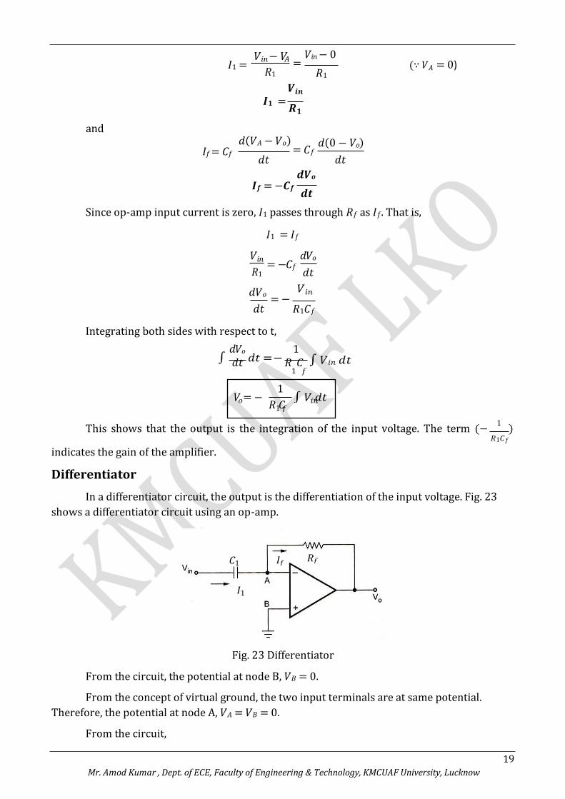
Integrator
In an integrator circuit, the output is the integration of the input voltage. Fig. 22 shows an
integrator circuit using an op-amp.
Fig. 22 Integrator
From the circuit, the potential at node B, 𝑉𝐵 = 0.
From the concept of virtual ground, the two input terminals are at same potential.
Therefore, the potential at node A, 𝑉𝐴 = 𝑉𝐵 = 0.
From the circuit,
1 𝑅 2 1
𝑅𝑓 − 𝑉 2
𝑅𝑓 𝑉𝑜 =
𝑅 𝑉
𝑅1
𝑅𝑓 𝑉2 − 𝑉1
𝑅𝑓(𝑅1 + 𝑅𝑓)
𝑅1(𝑅2 + 𝑅𝑓) 𝑉𝑜 =
𝑉𝑜 1 1 𝑉1
𝑅
𝑉𝑜
= 𝑉𝐴 ( + 𝑅1 𝑅𝑓
𝑅1 + 𝑅𝑓
) − 𝑅1
𝑉1
𝑅𝑓 = 𝑉𝐴 ( 𝑅1𝑅𝑓 ) − 𝑅
19
Mr. Amod Kumar , Dept. of ECE, Faculty of Engineering & Technology, KMCUAF University, Lucknow
1 𝑓 𝑖𝑛 ∫ 𝑉 𝑑𝑡
𝑅 𝐶 𝑜
1 𝑉 = −
𝐶1 𝐼𝑓 𝑅𝑓
𝐼1
𝐼1 =
𝑉𝑖𝑛 − 𝑉𝐴
𝑅1
𝑉𝑖𝑛 − 0 =
𝑅1
(∵ 𝑉𝐴 = 0)
𝑽𝒊𝒏
𝑰𝟏 = 𝑹
and
𝐼𝑓 = 𝐶𝑓
𝟏
𝑑(𝑉𝐴 − 𝑉𝑜)
= 𝐶𝑓 𝑑𝑡
𝒅𝑽𝒐
𝑑(0 − 𝑉𝑜)
𝑑𝑡
𝑰𝒇 = −𝑪𝒇
𝒅𝒕
Since op-amp input current is zero, 𝐼1 passes through 𝑅𝑓 as 𝐼𝑓. That is,
𝐼1 = 𝐼𝑓
𝑉𝑖𝑛
𝑅1
= −𝐶𝑓 𝑑𝑉𝑜
𝑑𝑡
𝑑𝑉𝑜
𝑑𝑡
𝑉𝑖𝑛 = −
𝑅1𝐶𝑓
Integrating both sides with respect to t,
𝑑𝑉𝑜 1 ∫ 𝑑𝑡 = − 𝑑𝑡 𝑅 𝐶 ∫ 𝑉𝑖𝑛 𝑑𝑡
1 𝑓
This shows that the output is the integration of the input voltage. The term (− 1
) 𝑅1𝐶𝑓
indicates the gain of the amplifier.
Differentiator
In a differentiator circuit, the output is the differentiation of the input voltage. Fig. 23
shows a differentiator circuit using an op-amp.
Fig. 23 Differentiator
From the circuit, the potential at node B, 𝑉𝐵 = 0.
From the concept of virtual ground, the two input terminals are at same potential.
Therefore, the potential at node A, 𝑉𝐴 = 𝑉𝐵 = 0.
From the circuit,

20 www.shrishailbhat.com Shrishail Bhat, Dept. of ECE, AITM Bhatkal
𝐼1 = 𝐶1
𝑑(𝑉𝑖𝑛 − 𝑉𝐴)
𝑑𝑡 = 𝐶1
𝒅𝑽𝒊𝒏
𝑑(𝑉𝑖𝑛 − 0)
𝑑𝑡
and
𝑰𝟏 = 𝑪𝟏
𝑉𝐴 − 𝑉𝑜
𝒅𝒕
0 − 𝑉𝑜 𝐼𝑓 =
𝑅𝑓 =
𝑽𝒐
𝑅𝑓
𝑰𝒇 = − 𝒇
Since op-amp input current is zero, 𝐼1 passes through 𝑅𝑓 as 𝐼𝑓. That is,
𝐼1 = 𝐼𝑓
𝑑𝑉𝑖𝑛 𝑉𝑜
𝐶1 = − 𝑑𝑡 𝑅𝑓
This shows that the output is the differentiation of the input voltage. The term (−𝑅𝑓𝐶1)
indicates the gain of the amplifier.
Comparator
In a comparator circuit, the amplitude of one voltage is compared with another. In this
application, op-amp is used in the open-loop configuration with the input voltage on one input
and reference voltage on the other. Fig. 24 shows a comparator circuit using an op-amp.
Here 𝑉2 = 𝑉𝑖𝑛 and 𝑉1 = 0.
Fig. 24 Comparator
When 𝑉𝑖𝑛 > 𝑉1 = 0, 𝑉𝑜 = +𝑉𝑠𝑎𝑡 ≅ +𝑉𝐶𝐶
When 𝑉𝑖𝑛 < 𝑉1 = 0, 𝑉𝑜 = −𝑉𝑠𝑎𝑡 ≅ −𝑉𝐸𝐸
Fig. 25 shows the input and output voltages.
𝑑𝑉𝑖𝑛 𝑉𝑜 = −𝑅𝑓𝐶1
𝑑𝑡
𝑹

21
Mr. Amod Kumar , Dept. of ECE, Faculty of Engineering & Technology, KMCUAF University, Lucknow
Fig. 25 Waveforms of comparator
The comparator circuit in Fig. 24 is also known as zero crossing detector.
Questions
1. What is an op-amp? Mention the applications of op-amp.
(Jun ’19, Jun ’18, Dec ’17, Dec ’16, Dec ’15, MQP ’15, MQP ’14)
2. Describe the characteristics of basic op-amp. List out its ideal characteristics.
(MQP ’18 – 8M)
3. What is op-amp? List out the ideal and practical characteristics of op-amp.
(Dec ’18 – 7M)
4. Explain the characteristics of an ideal op-amp.
(Jun ’19 – 6M, Dec ’18 – 5M, MQP ’18 – 8M, Jun ’18 – 5M, Dec ’17 – 6M, Jun ’17 – 4M, Dec
’16 – 6M, Jun ’16 – 7M, Dec ’15 – 4M, Jun ’15 – 6M, Dec ’14 – 5M, MQP ’15, MQP ’14 –
6M)
5. Explain the internal block diagram of an operational amplifier. (Dec ’18 – 6M, Jun ’16)
6. With neat circuit diagrams, explain the different input modes of an op-amp.
(Dec ’18 – 6M)
7. Explain the following terms related to op-amp: (i) Open loop voltage gain (ii) Common
mode gain (iii) CMRR (iv) Maximum Output Voltage Swing (v) Input Offset Voltage (vi)
Input Offset Current (vii) Input bias current (viii) Input impedance (ix) Output impedance
(x) Slew rate (xi) PSRR/Supply voltage rejection ratio (xii) Virtual ground.
(Jun ’19 – 8M, Dec ’18 – 8M, MQP ’18 – 10M, Jun ’18 – 6M, Dec ’17 – 5M, Jun ’16 – 5M,
Dec ’15 – 6M)
8. Write a short note on virtual ground concept of an op-amp. (Dec ’17 – 6M)
9. Explain the operation of an op-amp as an (i) Inverting amplifier (ii) Non inverting
amplifier. Derive an expression for the output voltage and voltage gain.
(Dec ’18 – 8M, Dec ’17 – 4M, Jun ’17 – 6M, Dec ’16 – 6M, Jun ’16 – 5M)
10. Draw the circuit of inverting op-amp. Derive the expression for the voltage gain.
(MQP ’18 – 8M, Jun ’18 – 7M, Dec ’17 – 5M)

22
Mr. Amod Kumar , Dept. of ECE, Faculty of Engineering & Technology, KMCUAF University, Lucknow
11. Explain the operation of an op-amp as a non-inverting amplifier with neat diagram and
waveforms. Derive the expression for output voltage.
(Dec ’18 – 6M, MQP ’18 – 6M, Jun ’18 – 4M)
12. With neat circuit and necessary equations, explain the voltage follower circuit using op-
amp. Mention its important properties.
(Jun ’19 – 4M, MQP ’18 – 4M, Dec ’17, Jun ’17 – 6M, Dec ’16 – 6M, Dec ’15 – 4M, Jun ’15
– 5M, MQP ’15 – 6M, MQP ’14)
13. Explain how an op-amp can be used as (i) Inverting summer (ii) Non inverting summer.
(Dec ’17, Jun ’17, MQP ’14)
14. Derive an expression for the output voltage of an inverting summer.
(Jun ’19, MQP ’18 – 6M)
15. Draw the three input inverting summer circuit and derive an expression for its output
voltage. (Dec ’18 – 5M, MQP ’18 – 8M, Dec ’17 – 5M, Dec ’15 – 5M, MQP ’15 – 5M)
16. Show with a circuit diagram, how an op-amp can be used as a subtractor.
(Jun ’19 – 4M, Dec ’18 – 8M, Dec ’16 – 8M)
17. With a neat circuit diagram, show how an op-amp can be used as an integrator. Derive
the expression for output voltage.
(Jun ’19 – 5M, Dec ’18 – 5M, MQP ’18 – 6M, Jun ’18 – 5M, Dec ’17 – 4M, Jun ’17 – 4M, Dec
’16, Jun ’16 – 6M, Dec ’15 – 6M, MQP ’14)
18. With a neat circuit diagram, show how an op-amp can be used as a differentiator. Derive
the expression for output voltage.
(Jun ’19 – 6M, MQP ’18 – 6M, Dec ’17, Dec ’16, Dec ’14 – 5M)
19. With a neat circuit diagram, show how an op-amp can be used as a comparator.
20. A certain op-amp has an open loop voltage gain of 1,00,000 and a common mode gain of
0.2. Determine the CMRR and express it in decibels. (MQP ’18 – 4M)
21. An op-amp has an open loop voltage gain of 104 and a common mode voltage gain of 0.1.
Express the CMRR in dB. (Jun ’16 – 8M)
22. Find the gain of a non-inverting amplifier if Rf = 10 kΩ and R1 = 1 kΩ. (Dec ’15 – 6M)
23. A non-inverting amplifier circuit has an input resistance of 10 kΩ and feedback resistance
60 kΩ with load resistance of 47 kΩ. Draw the circuit. Calculate the output voltage,
voltage gain, load current when the input voltage is 1.5 V. (Dec ’18 – 6M, MQP ’18 – 8M)
24. Design an inverting and non-inverting operational amplifier to have a gain of 15.
(Dec ’17 – 5M)
25. Calculate the output voltage of a three input inverting summing amplifier, given R1 =
200 kΩ, R2 = 250 kΩ, R3 = 500 kΩ, Rf = 1 MΩ, V1 = −2V, V2 = −1V and V3 = +3V.
(Dec ’18 – 5M, Jun ’16 – 4M)
26. Design an op-amp circuit to obtain output expression as Vo = −[V1 + 3V2 + 5V3].
(Jun ’19 – 6M)

23
Mr. Amod Kumar , Dept. of ECE, Faculty of Engineering & Technology, KMCUAF University, Lucknow
27. Design an adder circuit using op-amp to obtain an output expression
Vo = −[0.1V1 + 0.5V2 + 20V3], where V1, V2 and V3 are inputs. Select Rf = 10 kΩ.
(Jun ’19 – 7M, Jun ’18 – 6M)
28. Design an adder using op-amp to give the output voltage Vo = −[2V1 + 3V2 + 5V3].
(MQP ’18 – 6M, Dec ’17 – 6M)
29. Design an op-amp circuit that will produce an output equal to −[4V1 + V2 + 0.1V3].
(Dec ’17 – 6M)
30. Design an inverting summing circuit with feedback Rf = 100 kΩ using an op-amp to
generate the output Vo = −[3V1 + 4V2 + 5V3]. (Dec ’16 – 6M)
31. Design an adder circuit using op-amp to obtain an output voltage of
Vo = −[0.1V1 + 0.5V2 + 2V3], where V1, V2 and V3 are input voltages. Draw the circuit
diagram. (Jun ’15 – 8M)
32. The input to the basic differentiator circuit is a sinusoidal voltage of peak value of 10 mV
and frequency 1.5 kHz. Find the output if Rf = 100 kΩ and C1 = 1μF. (MQP ’18 – 4M)
33. Find the output of the op-amp circuit shown in the figure below. (Jun ’19 – 6M)
34. For an op-amp circuit shown in the figure, find the output Vo1 and Vo2. Also write the
function of each op-amp used. (Dec ’18 – 6M, MQP ’18 – 6M)
35. Find the output of the following op-amp circuit. (Jun ’18 – 5M)
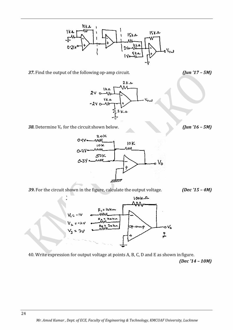
36. Find the output of the following op-amp circuit.
(Jun ’17 – 5M, Dec ’16 – 5M, MQP ’14 – 5M)
24
Mr. Amod Kumar , Dept. of ECE, Faculty of Engineering & Technology, KMCUAF University, Lucknow
37. Find the output of the following op-amp circuit. (Jun ’17 – 5M)
38. Determine Vo for the circuit shown below. (Jun ’16 – 5M)
39. For the circuit shown in the figure, calculate the output voltage. (Dec ’15 – 4M)
40. Write expression for output voltage at points A, B, C, D and E as shown in figure.
(Dec ’14 – 10M)

25
Mr. Amod Kumar , Dept. of ECE, Faculty of Engineering & Technology, KMCUAF University, Lucknow
41. Find the output of the following op-amp Circuit (MQP ’14 – 5M)
References
1. Thomas L. Floyd, “Electronic Devices”, Pearson Education, Ninth Edition, 2012.
2. D.P. Kothari, I. J. Nagrath, “Basic Electronics”, McGraw Hill Education (India) Private
Limited, 2014.
3. David A. Bell, “Operational Amplifiers and Linear IC’s”, 2nd edition, PHI/Pearson, 2004.
Recommended