Embed Size (px)
Citation preview

ABSTRACT
JIANG, YIFAN. Design, Fabrication and Characterization of High Voltage (>10 kV)4H-SiC MPS Diodes. (Under the direction of Dr. B. Jayant Baliga).
This work focuses on design, fabrication, characterization and optimization of 10
kilo-volts (kV) silicon carbide (SiC) Merged PiN/Schottky (MPS) rectifiers for grid ap-
plications like solid state transformers. The fundamentals of the application area and
the device are introduced, and the performance of the MPS diodes in almost all aspects
has been discussed. Two rounds of design and fabrication on silicon carbide high voltage
MPS diodes have been conducted and their characteristics have been evaluated.
In first round, Metal contact process was developed to make the Schottky contact
on n-type SiC and Ohmic contact on p-type SiC at the same time. The diodes with
different Schottky contact width were fabricated and characterized for comparison. With
the improvement quality of the Schottky contact and the passivation layer, the devices
show low leakage current up to 10 kV. The on-state characteristics from room temperature
to elevated temperature (423 K) was demonstrated and compared between structures
with different Schottky contact width. The switching behavior of the MPS diodes up to
473 K is revealed, and its reliability against bipolar degradation is evaluated.
To further improve its surge current capability, the device with different active area
layout, and the MPS diode with trench structure is proposed. The design of both the
active area and edge termination is introduced in detail, along with the process flows.
The basic performance of the fabricated devices is demonstrated.

© Copyright 2019 by Yifan Jiang
All Rights Reserved

Design, Fabrication and Characterization of High Voltage (>10 kV) 4H-SiC MPSDiodes
byYifan Jiang
A dissertation submitted to the Graduate Faculty ofNorth Carolina State University
in partial fulfillment of therequirements for the Degree of
Doctor of Philosophy
Electrical Engineering
Raleigh, North Carolina
2019
APPROVED BY:
Dr. Subhashish Bhattacharya Dr. Victor Veliadis
Dr. Douglas Hopkins Dr. B. Jayant BaligaChair of Advisory Committee

DEDICATION
To my parents Guorong Jiang and Yaxin Dai
ii

BIOGRAPHY
Yifan Jiang was born in haimen, jiangsu province in China. He received his B.S. degree in
electrical engineering from Tsinghua University in Beijing, China, at 2009. Then he came
to North Carolina State University as a graduate student and became a research assistant
at the Future Renewable Electric Energy Delivery and Management (FREEDM) Systems
Center in 2010. His research interests include the design, fabrication and characterization
study of power semiconductor devices.
…
iii

ACKNOWLEDGEMENTS
First, I would like to express my deepest gratitude to my advisor Dr. Jayant Baliga,
for his guidance, support and encouragement throughout my PhD career. His solid un-
derstanding on semiconductor physics, and extensive knowledge on all types of power
semiconductor devices, logical thinking and rigorous scholarship keeps influenced and
inspired me to develop my research.
I would like to thank Dr. Douglas Hopkins, Dr. Subhashish Battacharya, Dr. Victor
Veliadis and Dr. Ramon Collazo as my committee members. Their valuable advice with
expertise helps improve my research works.
I would like to thank Dr. Woongje Sung and Dr. Alex Huang as my mentors in my
first few years as a Ph.D candidate. Dr. Woongje Sung helps me a lot in getting involved
into the project and provide many valuable advice not only in technical details, but also
on how to be a qualified researcher in general. Every discussion with Dr. Alex Huang
has enlightened me in better understanding my research field and provided me a broader
vision.
It is always pleasure to work with great colleagues. I would like to thank specially
to previous FREEDM PSD team members Sizhen Wang, Inhwan Ji, Bongmook Lee,
Mengchia Lee, Haotao Ke, Adam Morgan and Xin Zhao for enlightening discussions. I
would also like to thank colleagues Xiaoqing Song, Liqi Zhang, Yang Xu, Siyang Liu,
Xuan Li, Junhong Tong in FREEDM.
I would like to thank all the staffs in NNF and AIF at NCSU and SMiF in Duke for
training and help in fabrication and characterization of my devices, and administratives in
FREEDM and ECE department, which are listed and not limited to: Greg Allion, Nicole
Hedges, Marcio Cerullo, Henry Taylor, Harold Madson, Bruce Sprague, Mark Walters,
iv

Jay Dalton, Kirk Bryson, Chuck Mooney, Karen Autry and Jessica Sudduth.
At last, I would like to thank my family, espeically my parents for their endless support
during the journey.
v

TABLE OF CONTENTS
LIST OF TABLES . . . . . . . . . . . . . . . . . . . . . . . . . . . . . . . . . . viii
LIST OF FIGURES . . . . . . . . . . . . . . . . . . . . . . . . . . . . . . . . . ix
Chapter 1 Introduction . . . . . . . . . . . . . . . . . . . . . . . . . . . . . . 11.1 FREEDM System and Solid-State Transformer . . . . . . . . . . . . . . 1
1.1.1 FREEDM System . . . . . . . . . . . . . . . . . . . . . . . . . . 11.1.2 Solid-State Transformer(SST) . . . . . . . . . . . . . . . . . . . . 2
1.2 SiC Power Semiconductor Devices . . . . . . . . . . . . . . . . . . . . . . 41.2.1 Wide Bandgap(WBG) Materials and Silicon Carbide . . . . . . . 41.2.2 Overview of Commercialized SiC Power Semiconductor Devices . 6
Chapter 2 High Voltage SiC Power Diodes . . . . . . . . . . . . . . . . . . 102.1 Basic Structures . . . . . . . . . . . . . . . . . . . . . . . . . . . . . . . 102.2 Theoretical Characteristics . . . . . . . . . . . . . . . . . . . . . . . . . . 14
2.2.1 Static Forward Characteristics . . . . . . . . . . . . . . . . . . . . 142.2.2 Leakage Current . . . . . . . . . . . . . . . . . . . . . . . . . . . 172.2.3 Switching Performance . . . . . . . . . . . . . . . . . . . . . . . . 192.2.4 Surge Performance . . . . . . . . . . . . . . . . . . . . . . . . . . 252.2.5 di/dt Capability . . . . . . . . . . . . . . . . . . . . . . . . . . . 32
Chapter 3 High Temperature Characterization of 10-kV SiC MPS Diodes 333.1 Device Structure . . . . . . . . . . . . . . . . . . . . . . . . . . . . . . . 333.2 Forward Characteristics . . . . . . . . . . . . . . . . . . . . . . . . . . . 343.3 Reverse Bias Leakage Current Characteristics . . . . . . . . . . . . . . . 353.4 Reverse Recovery Characteristics . . . . . . . . . . . . . . . . . . . . . . 393.5 Device Analysis . . . . . . . . . . . . . . . . . . . . . . . . . . . . . . . . 42
Chapter 4 Design, Fabrication and Characterization of 10-kV SiC MPSDiodes with High Schottky Barrier Height . . . . . . . . . . . 47
4.1 Device Design . . . . . . . . . . . . . . . . . . . . . . . . . . . . . . . . . 474.1.1 Aluminum Ion Implantation . . . . . . . . . . . . . . . . . . . . . 474.1.2 Basic Cell Design . . . . . . . . . . . . . . . . . . . . . . . . . . . 514.1.3 Edge Termination Design . . . . . . . . . . . . . . . . . . . . . . 53
4.2 Fabrication Procedure . . . . . . . . . . . . . . . . . . . . . . . . . . . . 584.2.1 Starting Material . . . . . . . . . . . . . . . . . . . . . . . . . . . 584.2.2 Experiment with Metal Contact . . . . . . . . . . . . . . . . . . . 594.2.3 Mask Layout . . . . . . . . . . . . . . . . . . . . . . . . . . . . . 614.2.4 Process Flow . . . . . . . . . . . . . . . . . . . . . . . . . . . . . 61
vi

4.3 Characterization Results and Analysis . . . . . . . . . . . . . . . . . . . 654.3.1 Schottky Barrier . . . . . . . . . . . . . . . . . . . . . . . . . . . 654.3.2 Temperature Dependent Forward Characteristics . . . . . . . . . 654.3.3 Reverse Characteristics . . . . . . . . . . . . . . . . . . . . . . . 704.3.4 Reverse Recovery Characteristics . . . . . . . . . . . . . . . . . . 774.3.5 Reliability . . . . . . . . . . . . . . . . . . . . . . . . . . . . . . . 804.3.6 Device Modeling . . . . . . . . . . . . . . . . . . . . . . . . . . . 82
Chapter 5 Design and Fabrication of 10-kV SiC MPS Diodes with Im-proved Structures . . . . . . . . . . . . . . . . . . . . . . . . . . . 85
5.1 Device Design . . . . . . . . . . . . . . . . . . . . . . . . . . . . . . . . . 855.1.1 Active Cell Design . . . . . . . . . . . . . . . . . . . . . . . . . . 855.1.2 Edge Termination Design . . . . . . . . . . . . . . . . . . . . . . 875.1.3 Layout Design . . . . . . . . . . . . . . . . . . . . . . . . . . . . 88
5.2 Fabrication Procedure . . . . . . . . . . . . . . . . . . . . . . . . . . . . 925.2.1 Starting Material . . . . . . . . . . . . . . . . . . . . . . . . . . . 925.2.2 Design of Process Flow . . . . . . . . . . . . . . . . . . . . . . . . 93
5.3 Characterization Results . . . . . . . . . . . . . . . . . . . . . . . . . . . 975.3.1 Forward Characteristics . . . . . . . . . . . . . . . . . . . . . . . 975.3.2 Reverse Characteristics . . . . . . . . . . . . . . . . . . . . . . . 985.3.3 Surge Current Test Design . . . . . . . . . . . . . . . . . . . . . . 101
Chapter 6 Conclusion and Future Work . . . . . . . . . . . . . . . . . . . . 104
References . . . . . . . . . . . . . . . . . . . . . . . . . . . . . . . . . . . . . . . 106
Appendix . . . . . . . . . . . . . . . . . . . . . . . . . . . . . . . . . . . . . . . 118Appendix A Models for Numerical Simulation of 4H-SiC Power Devices . . . 119
A.1 Simulation Models . . . . . . . . . . . . . . . . . . . . . . . . . . . 119
vii

LIST OF TABLES
Table 1.1 Properties of Materials for Making Power Semiconductor Devices . . . . . 5Table 1.2 Performance comparison of commercial 650V SiC Schotttky diodes based on
datasheet ∗ the surge test was done at 8.3 msec half-sinusoidal current waveinstead of 10 msec . . . . . . . . . . . . . . . . . . . . . . . . . . . . . . 7
Table 1.3 Performance comparison of commercial 1200V SiC Schotttky diodes basedon datasheet ∗ the surge test was done at 8.3 msec half-sinusoidal currentwave instead of 10 msec . . . . . . . . . . . . . . . . . . . . . . . . . . . 8
Table 1.4 Performance comparison of commercial 1200V SiC MOSFETs based on datasheet9
Table 2.1 comparison of forward performance of 10 kV power diodes from literature . 12Table 2.2 comparison of reverse performance of 10 kV power diodes from literature . 13Table 2.3 Mechanisms of leakage current for SiC Schottky diodes at different locations 20Table 2.4 comparison of parameters of diode reverse recovery . . . . . . . . . . . . . 22Table 2.5 comparison of surge capability between various commercial high power sili-
con diodes . . . . . . . . . . . . . . . . . . . . . . . . . . . . . . . . . . 25
Table 4.1 Extracted SBH and ideality factor of the Schottky metal on n-type regionand the Ohmic contact resistance formed at the same time on the p-typeregion . . . . . . . . . . . . . . . . . . . . . . . . . . . . . . . . . . . . 60
Table 4.2 Comparison of single and separate metal process for Ohmic and Schot-tky contact on the MPS diode . . . . . . . . . . . . . . . . . . . . . . 61
Table 4.3 Fabrication Procedure . . . . . . . . . . . . . . . . . . . . . . . . . . . 64Table 4.4 Device types with different contact widths . . . . . . . . . . . . . . . . 67Table 4.5 Relationship of parameters during diode reverse recovery . . . . . . . 79
Table 5.1 comparison of recipe for etching silicon carbide by Oxford NGP80 at NNF 95Table 5.2 Fabrication Procedure . . . . . . . . . . . . . . . . . . . . . . . . . . . 96
Table A.1 Simulation Models and Parameters . . . . . . . . . . . . . . . . . . . . . 120
viii

LIST OF FIGURES
Figure 1.1 The interface of a future home in FREEDM System . . . . . . . . . . 2Figure 1.2 Circuit Diagram of the Gen II SST . . . . . . . . . . . . . . . . . . . 4
Figure 2.1 Schematic cross section of the (a) JBS diode (b) MPS diode (c) PiNdiode . . . . . . . . . . . . . . . . . . . . . . . . . . . . . . . . . . . . 12
Figure 2.2 TCAD simulation of reverse I-V characteristics of 15 kV SiC Schot-tky diodes (a) with different Schottky barrier heights at 200 oC (b)JBS/MPS with different half-cell spaces (µm) between junctions withSBH of 1.7 eV . . . . . . . . . . . . . . . . . . . . . . . . . . . . . . 18
Figure 2.3 simplified circuit diagram of double pulse test in LTspice . . . . . . . 21Figure 2.4 diode turn-off waveforms with standard model and model with two
times junction capacitance . . . . . . . . . . . . . . . . . . . . . . . 21Figure 2.5 Mixed-mode simulation of the reverse recovery performance of 10 kV
SiC MPS diodes . . . . . . . . . . . . . . . . . . . . . . . . . . . . . 23Figure 2.6 Distribution of minority carriers within the drift region under the mid-
dle of Schottky contact when voltage starts to rise . . . . . . . . . . . 24Figure 2.7 forward characteristics of the high voltage JBS/MPS diodes with vary-
ing Wo at (a) 300K (b) 473K . . . . . . . . . . . . . . . . . . . . . . 28Figure 2.8 the voltage and temperature waveform of diodes with various Wo at
300K . . . . . . . . . . . . . . . . . . . . . . . . . . . . . . . . . . . 29Figure 2.9 the voltage and temperature waveform of diodes with various Wo at
473K . . . . . . . . . . . . . . . . . . . . . . . . . . . . . . . . . . . 29Figure 2.10 forward characteristics of the high voltage JBS/MPS diodes with wide
and narrow contact coverage at 300K and 473K . . . . . . . . . . . . 30Figure 2.11 hole current density close to the top surface of the 10 kV SiC MPS
diodes with (a) wide (b) narrow contact . . . . . . . . . . . . . . . . 31Figure 2.12 the voltage and temperature waveform of diodes with wide and narrow
Ohmic contact at surge condition at 300 K and 473 K . . . . . . . . 31
Figure 3.1 Measured forward I-V of the PiN JBS and MPS at room temperatureand high temperature (200 C) . . . . . . . . . . . . . . . . . . . . . 35
Figure 3.2 Forward voltage drop of the PiN, JBS and MPS diodes at 20A/cm2 . 36Figure 3.3 Measured reverse I-V of the PiN JBS and MPS diode at room tem-
perature and 125 C . . . . . . . . . . . . . . . . . . . . . . . . . . . 37Figure 3.4 Measured reverse I-V of the MPS diode from room temperature to 200
C . . . . . . . . . . . . . . . . . . . . . . . . . . . . . . . . . . . . . 37Figure 3.5 Multiple time measurement of reverse I-V of the PiN diode die at room
temperature . . . . . . . . . . . . . . . . . . . . . . . . . . . . . . . . 38
ix

Figure 3.6 Multiple time measurement of reverse I-V of the PiN diode die at (a)75 C and (b) 125 C . . . . . . . . . . . . . . . . . . . . . . . . . . 39
Figure 3.7 Test Set-up for measurement of reverse recovery . . . . . . . . . . . 40Figure 3.8 The reverse recovery waveform of SiC (a) MPS (b) diode at different
temperature . . . . . . . . . . . . . . . . . . . . . . . . . . . . . . . . 41Figure 3.9 Measured reverse recovery charge of PiN and MPS diodes. . . . . . . 41Figure 3.10 The Trade-off Curve Between Reverse Recovery Charge and Forward
Voltage of SiC PiN and MPS diode at different temperature(C) . . 42Figure 3.11 Forward IV of the MPS diode with different local lifetime in the ion
implantation region . . . . . . . . . . . . . . . . . . . . . . . . . . . 43Figure 3.12 Forward IV of the MPS and PiN diodes though numerical simulation
at room temperature and 200 C . . . . . . . . . . . . . . . . . . . . 44Figure 3.13 Minority carrier concentration in the drift region of PiN and MPS at
25 C and 200 C for an on-state current density of 10 A/cm2 . . . . 45Figure 3.14 Stored charge of PiN and MPS diodes at 10A/cm2 from numerical
simulation at different temperatures . . . . . . . . . . . . . . . . . . . 46
Figure 4.1 Comparison between Pearson Function [1] and Monte Carlo Simula-tion of Al impurity concentration profile at vertical direction . . . . . 48
Figure 4.2 SEM image of the fabricated 10 kV SiC JBS diode with drift regiondoping of 8× 1014 cm-3 . . . . . . . . . . . . . . . . . . . . . . . . . . 50
Figure 4.3 Al active concentration contour with oxide mask (a) total dose of 3.6×1015 cm-2(b) total dose of 2× 1013 cm-2 . . . . . . . . . . . . . . . . . 51
Figure 4.4 Forward characteristics of 10 kV SBD with different Schottky barrierheight at room temperature . . . . . . . . . . . . . . . . . . . . . . . 52
Figure 4.5 Forward characteristics of 10 kV MPS diodes with Ws = 0.5 µm at (a)room temperature (b) 473 K . . . . . . . . . . . . . . . . . . . . . . 53
Figure 4.6 Current densities of MPS diodes at Vf = 6V with Schottky barrierheight of (a) 1.0 eV and (b) 1.6 eV at 473 K . . . . . . . . . . . . . . 54
Figure 4.7 Simulation structure close to the anode for FFR edge termination (a) with-out and (b) with including lateral straggling effect . . . . . . . . . . . . 55
Figure 4.8 Schematic illustration of three kinds of edge termination for 10 kV device(a) multiple FFR (b) MFZ-JTE (c) Hybrid JTE . . . . . . . . . . . . . 55
Figure 4.9 SEM image of the edge termination area of the fabricated 10 kV SiCJBS diode with drift region doping of 8× 1014 cm-3 . . . . . . . . . . 56
Figure 4.10 Comparison of the electric field distribution along the FFR edge termination(y=0.3) at 10 kV with different interface charges without lateral straggling 56
Figure 4.11 Comparison of the electric field distribution along the FFR edge termination(y=0.3) at 10 kV with different interface charges with lateral straggling . . 56
Figure 4.12 Simulated breakdown voltage with different interface charges for thethree kinds of edge termination . . . . . . . . . . . . . . . . . . . . . 58
x

Figure 4.13 Map of measured minority lifetime by µPCD method . . . . . . . . . 59Figure 4.14 Schematic mask layout for fabrication of the MPS diodes . . . . . . . 62Figure 4.15 The layout of the wafer with repetitive blocks . . . . . . . . . . . . . 62Figure 4.16 (a) wafer picture (b) microscope picture of patterned edge termination
region before ion implantation . . . . . . . . . . . . . . . . . . . . . . 63Figure 4.17 forward IV characteristics of the Schottky test structure with active
area of 3.36×10⁻³cm2 . . . . . . . . . . . . . . . . . . . . . . . . . . 66Figure 4.18 (a) Distribution of extracted Schottky contact barrier height and ide-
ality factor on the wafer (b) Relationship between Schottky barrierheight and ideality factor . . . . . . . . . . . . . . . . . . . . . . . . . 66
Figure 4.19 Box chart of the range distribution of forward voltage of different typesof devices with an active area of 6.68 mm2 at 20 A/cm2 and roomtemperature . . . . . . . . . . . . . . . . . . . . . . . . . . . . . . . . 68
Figure 4.20 Forward current voltage characteristics of different types of diodestested on wafer at room temperature (b) the close up graph at lowcurrent density up to 5 A/cm2 . . . . . . . . . . . . . . . . . . . . . . 68
Figure 4.21 Forward current voltage characteristics of different types of diodestested on wafer at 423 K (b) the close up graph at low current densityup to 5 A/cm2 . . . . . . . . . . . . . . . . . . . . . . . . . . . . . . 69
Figure 4.22 (a) Forward voltage of different types of diodes at 20 A/cm2 (b) Dif-ferential on-resistance at 20 A/cm2 for different types of diodes atdifferent temperature tested on wafer . . . . . . . . . . . . . . . . . . 69
Figure 4.23 Packaged silicon carbide MPS diodes for high temperature operationwith thermistor . . . . . . . . . . . . . . . . . . . . . . . . . . . . . . 70
Figure 4.24 Forward I-V characteristics of a packaged MPS diode (D1) at elevatingtemperature up to 498 K . . . . . . . . . . . . . . . . . . . . . . . . . 71
Figure 4.25 Distribution of breakdown voltage (V) of (a) PiN diodes and (b) Schot-tky diodes top half of the tested wafer . . . . . . . . . . . . . . . . . 72
Figure 4.26 Distribution of breakdown voltage (V) of (a) MPS diodes and (b) JBSdiodes on top half of the tested wafer . . . . . . . . . . . . . . . . . . 72
Figure 4.27 Reverse I-V characteristics of for different types of devices with anactive area of 6.68 mm2 at room temperature . . . . . . . . . . . . . 73
Figure 4.28 Distribution of breakdown voltage (V) of small MPS diodes with dif-ferent edge termination designs (a) Si = 0.0175 um (b) Si = 0.0225um (c) Si = 0.0275 um on top half of the tested wafer . . . . . . . . . 74
Figure 4.29 Reverse I-V characteristics of MPS(D1) with small active area (1.13mm2) with different edge termination design . . . . . . . . . . . . . . 75
Figure 4.30 The leakage current under 5 kV for small MPS diodes before and afterpolyimide passivation . . . . . . . . . . . . . . . . . . . . . . . . . . . 75
xi

Figure 4.31 Reverse I-V characteristics of for different types of devices comparedto previous work [2] . . . . . . . . . . . . . . . . . . . . . . . . . . . 76
Figure 4.32 forward voltage and leakage current of MPS diode compared to pre-vious work [2] . . . . . . . . . . . . . . . . . . . . . . . . . . . . . . . 76
Figure 4.33 First and second time test of (a) SBD and (b) PiN diode reverse I-Vwith time gap of over 12 hours . . . . . . . . . . . . . . . . . . . . . 77
Figure 4.34 Reverse I-V characteristics of for MPS diodes at various temperature 78Figure 4.35 Double pulse test setup with the high voltage MPS diodes . . . . . . 79Figure 4.36 Reverse recovery characteristics of MPS diode (D1) at different tem-
perature with gate resistance (a) 20 Ω (b) 100 Ω . . . . . . . . . . . . 79Figure 4.37 The reverse recovery charge (Qrr versus forward voltage Vf of MPS
diode (D1) with increasing temperature) . . . . . . . . . . . . . . . . 80Figure 4.38 The forward voltage drift of the different devices (three MPS diodes(D1),
one JBS diode(D3)) at 30 A/cm2 after the DC stress at 75 A/cm2 for6 hours . . . . . . . . . . . . . . . . . . . . . . . . . . . . . . . . . . 81
Figure 4.39 Comparison of the measured forward I-V characteristics to TCADsimulation results of PiN(D0), MPS(D1) and JBS(D4) at room tem-perature . . . . . . . . . . . . . . . . . . . . . . . . . . . . . . . . . 83
Figure 4.40 Comparison of the measured reverse I-V characteristics to TCAD sim-ulation results of SBD(D5) at room temperature . . . . . . . . . . . . 84
Figure 5.1 Comparison of forward characteristics of 10 kV conventional and trenchMPS diodes with different Schottky contact width Ws at (a) 300 K(b) 473 K . . . . . . . . . . . . . . . . . . . . . . . . . . . . . . . . . 87
Figure 5.2 basic cell parameters in hex structure design . . . . . . . . . . . . . . 88Figure 5.3 Orginal MFZ-JTE design for SiC high voltage devices [3] . . . . . . . 89Figure 5.4 Similar MFZ-JTE structure with first 16 rings merged . . . . . . . . 89Figure 5.5 Simulated breakdown voltage of MFZ-JTE with different interface
charges (IC) (cm−2), doses, and α . . . . . . . . . . . . . . . . . . . . 90Figure 5.6 layout design for stripe and hex structures with large p-type areas . . 92Figure 5.7 closer look on the layout design with parameters labeled . . . . . . . 93Figure 5.8 Map of measured minority lifetime by µPCD method . . . . . . . . . 94Figure 5.9 Forward current voltage characteristics of different types of diodes
tested on wafer with active area of 6.68 mm2 . . . . . . . . . . . . . . 98Figure 5.10 Forward current voltage characteristics of the diode test structure with
whole active area covered with Schottky contact . . . . . . . . . . . . 99Figure 5.11 (a) the I-V curve of between the contacts of the TLM structures with
different space; (b) The extracted resistance versus spaces and thelinear fit results . . . . . . . . . . . . . . . . . . . . . . . . . . . . . . 99
Figure 5.12 Distribution of breakdown voltage (V) of diodes tested on sample withALD oxide and polyimide as passivation layers . . . . . . . . . . . . . 100
xii

Figure 5.13 Reverse I-V characteristics of for MPS diodes with different edge ter-mination design and Ws (active area 6.68 mm2) . . . . . . . . . . . . 101
Figure 5.14 Distribution of breakdown voltage (V) of diodes tested on sample withtrench structure and only polyimide as passivation . . . . . . . . . . 102
Figure 5.15 Reverse I-V characteristics of for trench devices with active area of6.68 mm2 and α of 1.02 . . . . . . . . . . . . . . . . . . . . . . . . . 102
xiii

Chapter 1
Introduction
1.1 FREEDM System and Solid-State Transformer
1.1.1 FREEDM System
The Future Renewable Electric Energy Delivery and Management(FREEDM) System is
an architecture proposed for a future electric power distribution, which is suitable for
plug-and-play of distributed renewable energy and distributed energy storage devices
[4, 5]. Figure 1.1 shows the electric grid diagram conceptualizing the FREEDM system.
The key feature contains a plug-and-play interface that includes both a 400-V DC bus
and a conventional 220V AC bus, an intelligent energy management (IEM) device and
an open-standard-based operating system called the distributed grid intelligence (DGI).
The IEM device acts as the energy router, which is actually formed by a solid-state
transformer(SST), which will be introduced in the next section. The IEM device performs
power and energy control and voltage step-down function the DGI software and the
communication interface. The subsystems connected by SSTs are distributed renewable
1
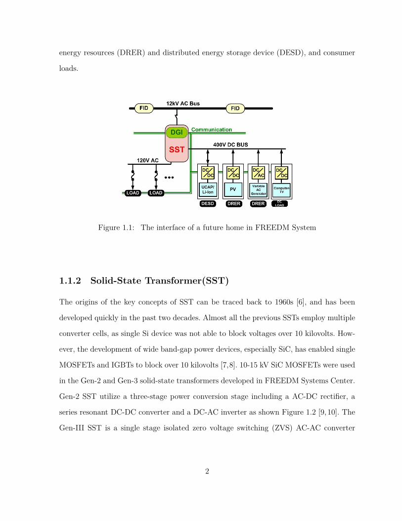
energy resources (DRER) and distributed energy storage device (DESD), and consumer
loads.
Figure 1.1: The interface of a future home in FREEDM System
1.1.2 Solid-State Transformer(SST)
The origins of the key concepts of SST can be traced back to 1960s [6], and has been
developed quickly in the past two decades. Almost all the previous SSTs employ multiple
converter cells, as single Si device was not able to block voltages over 10 kilovolts. How-
ever, the development of wide band-gap power devices, especially SiC, has enabled single
MOSFETs and IGBTs to block over 10 kilovolts [7,8]. 10-15 kV SiC MOSFETs were used
in the Gen-2 and Gen-3 solid-state transformers developed in FREEDM Systems Center.
Gen-2 SST utilize a three-stage power conversion stage including a AC-DC rectifier, a
series resonant DC-DC converter and a DC-AC inverter as shown Figure 1.2 [9,10]. The
Gen-III SST is a single stage isolated zero voltage switching (ZVS) AC-AC converter
2

design which was aimed for demonstration of higher efficiency and higher power den-
sity [11]. Due to the proper ZVS design, no parallel diodes were used at the high voltage
side.
The basic loss calculation of the diodes can be described as:
Ploss = PconD + Pswfsw (1.1)
Where D is the duty ratio when diode is turned on and fsw is the switching frequency.
The off state loss was neglected as it is usually much smaller than the conduction loss
and switching loss for silicon carbide devices. The higher switching frequency will cause
a bigger part of the switching loss in the total loss. In power diodes, there are always
trade-off between conduction loss and switching loss, especially for bipolar diodes. For a
fixed device structure, a lower conduction loss (lower Rdson) will always cause a higher
switching loss (mainly from reverse recovery process for bipolar diodes). However, the
trade off can be different for different device structures, and it also depends on the switch-
ing frequency. Another factor is the temperature which is usually not often discussed.
For the bipolar devices, the performance both at conduction and switching state can vary
significantly with temperature, and the device is always favored to be able to work at
higher temperature (200 C and higher) as long as the system(module) can withstand it.
It will help minimize the size and cost of cooling systems, and is also required in some
extreme environments. In that case, the loss at high temperature should be considered as
it is closer to the operating conditions. The detailed trade-off performance of SiC diodes
will be discussed in the following chapters.
3

Figure 1.2: Circuit Diagram of the Gen II SST
1.2 SiC Power Semiconductor Devices
1.2.1 Wide Bandgap(WBG) Materials and Silicon Carbide
For any semiconductors, there is a distance between the bottom of conduction band and
top of valance band, which is called the bandgap. Ideally no energy states are allowed
in this region. The wide bandgap materials are favored for making power semiconductor
devices, and the reasons are:
1. wide bandgap materials have much lower intrinsic carrier concentrations. The rela-
tionship between the intrinsic carrier concentration and bandgap is shown below:
ni =√
NCNV exp(−Eg
2kT) (1.2)
It decreases exponentially with the wider bandgap. The intrinsic carrier concentra-
tion is closely related to the leakage current, which makes the leakage current of
4

the WBG power semiconductors much lower than Si, even with higher dislocation
densities which may contribute to higher leakage current [12].
2. Generally, the impact ionization rate is decreasing with increasing bandgap. This
is the most important reason for the use of wide band gap materials for power
devices. The low ionization rate at high electric field makes the wide band gap
semiconductor devices having a higher breakdown voltage [13]. For two devices
with the same breakdown voltage, the one made using wide bandgap materials
can have a much lower on-state resistance, so the on-state loss is much lower, thus
makes whole power electronic systems much more efficient.
Currently the most popular materials for making wide bandgap power devices are
4H-SiC and GaN. There are also new materials like Ga2O3 and diamond being studied.
The basic electrical and thermal properties of these materials are compared below:
Table 1.1: Properties of Materials for Making Power Semiconductor Devices
SemiconductorMaterials
EnergyBandgap
(eV)
RelativeDielectricConstant
ThermalConductivity(W/cm-K)
Melting Point(K)
Si 1.1 11.7 1.3-1.5 16854H-SiC 3.3 9.7 4 ~31002H-GaN 3.4 8.9 1.3 2800β-Ga2O3 4.9 ~10 0.13-0.23 1998Diamond 5.5 5.7 20 ~4650
One big challenge for making wide bandgap semiconductor devices is that it is hard
to grow a defect-free crystal with large area like silicon. Silicon can be formed monocrys-
talline with less strong covalent bond, and the wide application of integrated circuits has
made the single crystal silicon in high demand. For compounds like silicon carbide, it
5

has multiple polytypes of crystal, so that the temperature and gas flow has to be con-
trolled more precisely and uniformly compared to silicon. Currently even the commercial
silicon carbide crystal for power devices (mainly 4H-SiC) has much larger defect density
compared to silicon.
1.2.2 Overview of Commercialized SiC Power Semiconductor
Devices
There have been many reviews about the silicon carbide power devices [14,15]. Currently
the Schottky diodes and MOSFETs have been commercialized by many companies, and
starts to be accepted by the power electronic industries. Here a simple comparison of
these diodes and and MOSFETs is shown here. For the silicon carbide Schottky diodes,
almost all the companies utilized the Junction Barrier Schottky(JBS) concept. At 650
V rated voltage range, the comparison is shown in Table 1.2 with all the diodes with
maximum operating temperature of 175 C.
All the numbers at taken at rated current or rated blocking voltage (650V). Rdson’
means the on-state resistance was calculated by forward voltage divided by current at on-
state rating instead of the differential on-resistance. Most of their properties are close to
each other from different companies. The Wolfspeed’s C5D50065D shows the highest Non-
repetitive surge capability, and it is eight times the current rating. The same comparison
was done on 1200 V SiC Diodes, as shown in Table 1.3.
Rohm’s diodes show slightly lower forward voltage compared to other 20A devices.
The 1200V diodes from OnSemi has the lowest leakage current both at room and high
temperature compared to other diodes. At ratings of 1200 V, Infineon’s IDH20G120C5
shows the highest non-repetitive surge capability compared to other products.
6

Table 1.2: Performance comparison of commercial 650V SiC Schotttky diodes based ondatasheet ∗ the surge test was done at 8.3 msec half-sinusoidal current wave instead of 10msec
CompanyProduct No
Gen-eration
CurrentRat-ing/A
ForwardVoltage
at25/175C /V
Rdson’·Cat 1/400V /psec
Vf·Qc/nVolt·C
Irated/Ileakage
at25/175C(×106)
Non-Repetitive
SurgeCapabil-ity 10ms
/AWolfspeed
CPW5-0650-Z030B
CPW5 30 1.6/2.2 60.64/5.87 104 1.5/0.5 N/A
WolfspeedC5D50065D C5D 50 1.5/1.8 59.1/5.4 165 1/0.25 400
InfineonIDW40G65C5 5th 40 1.5/2 42.8/5.44 82.5 18.2/4.88 182
InfineonIDH20G65C6 6th 20 1.25/1.6 60.63/3.5 33.5 4/0.03 99
RohmSCS220AJHR 2nd 20 1.35/1.63 49.28/5.2 41.9 5/0.1 71∗
RohmSCS320AHG 3rd 20 1.35/1.5 67.5/6.41 63.45 333/1.67 123
OnSemiFFSH5065A N/A 50 1.51/1.82 76.4/6.37 222 100/10 230∗
7

Table 1.3: Performance comparison of commercial 1200V SiC Schotttky diodes based ondatasheet ∗ the surge test was done at 8.3 msec half-sinusoidal current wave instead of 10msec
CompanyProduct No
Gen-eration
CurrentRat-ing/A
ForwardVoltage
at25/175C /V
Rdson’·Cat 1/800V /psec
Vf·Qc/nVolt·C
Irated/Ileakage
at25/175C(×106)
Non-Repetitive
SurgeCapabil-ity 10ms
/AWolfspeed
C4D20120A C4D 20 1.5/2.2 112.5/5.03 148.5 0.57/0.31 130
WolfspeedCPW5-
1200-Z050DCPW5 50 1.6/2.25 108.2/5.54 393.6 0.5/0.17 N/A
InfineonIDH20G120C5 5th 20 1.5/2.0 78.75/4.43 123 2.35/0.45 198
RohmSCS240KE2A-
HR2nd 20 1.4/1.9 73.5/5.88 92.4 1/0.077 78
OnSemiFFSP20120A N/A 20 1.45/2 88.45/6.38 174 4/1 135∗
8

The comparison for 1200V SiC MOSFET is shown in Table 1.4. It is worth noticing
that the test conditions for some parameters on Datasheet are not the same, like the
current level for test of Qg and Qrr of the body diode. The SiC MOSFETs from Wolfspeed
shows the lowerest high frequency figure of merit(FOM), defined as RdsonCgd [16]. The
one from Infineon and Rohm shows higher threshold voltage of larger than 4 volt, which
is important in actual power electronic systems to avoid false turn-on of the device. ST
is the only company which has SiC MOSFETs being able to operate at 200 C.
Table 1.4: Performance comparison of commercial 1200V SiC MOSFETs based on datasheet
CompanyProduct No
Gen-eration
CurrentRat-ing/A
Rdsonat
25/150C
/mOhm
Rdson·Cgd/psec
Rdson·Qg
/nVolt·C
Thres-holdVolt-age/V
BodydiodeQrr/nC
Maximumjunctiontemper-ature/C
WolfspeedC2M0025120D C2M 90 25/43 0.375 4.025 2.6 220 150
WolfspeedC3M0075120K C3M 30 75/100 0.225 3.825 2.5 406 150
InfineonFF11MR12W-
1M1-B111st 100 110/165 5.72 27.5 4.5 N/A 150
RohmSCT3022KL 3rd 95 22/40 2.376 3.916 4.2 175 175
STSCT50N120 N/A 20 52/59 1.56 6.344 3 230 200
Overall, currently the voltage ratings of the mass produced SiC power devices are
limited under 2 kV. There are still not much research works about >10 kV SiC power
devices. In this thesis, we will be focusing on the >10 kV SiC power diodes for applications
like solid-state transformers.
9

Chapter 2
High Voltage SiC Power Diodes
2.1 Basic Structures
For SiC power diodes, there have been many uncommon structures proposed, like dual
metal trench Schottky rectifier (TSBS) [17], trench MOS barrier Schottky rectifier(TMBS)
[18], Pinch Rectifier [19] and Static-Shielded Diode [20]. However, the structures of com-
mercialized devices so far are junction barrier Schottky (JBS) diode and merged PiN
Schottky (MPS) diode, due to ease of processing, robustness and good performance un-
der 600 V - 1700 V. These two concepts were originally proposed for silicon power de-
vices [21,22], and the schematic cross section is shown in Figure 2.1. In the JBS structure,
the added counter-doped region near the surface with certain spaces mainly shields the
electric field right under the Schottky contact to have the lower leakage current. The
MPS diode has the similar structure as JBS diode, and the only difference is that the
counter-doped region(usually p-type) also serves as a current path by injecting minority
carriers at on-state, so that the total on-resistance can be reduced. In this case, the MPS
diodes are also bipolar devices. The p-type regions in JBS/MPS diodes are typically
10

formed by ion implantation. PiN diode is frequently discussed for SiC diodes especially
with voltage ratings of over 10 kV [23, 24]. For fabricating the PiN diodes, the p-type
region can be formed either by ion implantation or epitaxial growth. Different processes
will lead to different electrical characteristics, which will be discussed in the following
sections.
Another approach has been demonstrated recently by using a hybrid concept of
putting the epitaxial p-type region and JBS cells together on the active area but with dif-
ferent regions [25]. The forward characteristics is very similar to traditional MPS diodes,
with low on-state resistances. Nevertheless, the switching behavior of that structure has
not been discussed. Compared to traditional MPS diodes, this structure needs extra epi-
taxial and etching steps. At high current densities, most of the current comes from the
epitaxial p-type region, which may cause temperature to be high at localized region in-
stead of distributing more evenly over the total active area in traditional MPS structures.
Table 2.1 and Table 2.2 presents comparison of performance of diodes from literature.
From Table 2.1, the pin diode has significant advantage over JBS structure on forward
voltage at same current densities, means the chip size can be much smaller with the same
current rating. With lifetime enhancement process, the forward voltage of pin diode at
100 A/cm2 can be as low as less than 4 V. Cree showed their both 10 kV pin and JBS
diodes with large areas. In terms of reverse I-V performance, different institutions showed
various edge termination structures and results. The result from chapter 4 and 5 shows
high breakdown voltage and low leakage current with relatively thin drift regions.
11

Figure 2.1: Schematic cross section of the (a) JBS diode (b) MPS diode (c) PiN diode
Table 2.1: comparison of forward performance of 10 kV power diodes from literature
YearInstitution structure
drift regionthickness
and dopingconcentra-
tion
forwardvoltage(V) @100
A/cm2
lifetime(µsec)
chiparea
2017Kyoto
University[25]
hybridMPS
95 µm 6e14cm−3 4.5 10 0.36
mm2
2005Cree [26]
epitaxialPiN
100 µm 2e14cm−3 3.75 10 75.6
mm2
2015KTH [24]
on-axisPiN
100 µm 7e14cm−3 3.3 1.15 7.85e-3
mm2
2013AIST [27]
epitaxialPiN
120 µm 5e14cm−3 5.3 0.06 64
mm2
2008Cree [28] JBS 120 µm 6e14
cm−3 16.25 N/A 150mm2
2013Genesic
[29]
epitaxialPiN
130 µm6-7e14 cm−3 6 5 5.76
mm2
2016AIST [30] JBS 150 µm 5e14
cm−3 29 N/A 25mm2
12

Table 2.2: comparison of reverse performance of 10 kV power diodes from literature
YearInstitution structure
drift regionthickness
and dopingconcentra-
tion
breakdownvoltage
leakagecurrent
edgetermination
structure andwidth (µm)
2017Kyoto
University[25]
hybridMPS
95 µm 6e14cm−3 11.3 kV
0.7mA/cm2
@ 10 kV
space-modulated JTE
with 500 µm
2005Cree [26]
epitaxialPiN
100 µm 2e14cm−3 10 kV 1 mA/cm2 N/A 850 µm
2015KTH [24]
on-axisPiN
100 µm 7e14cm−3 > 10 kV 0.2 µA @
10 kVthree-zone JTE
1050 µm2013
AIST [27]epitaxial
PiN120 µm 5e14
cm−3 13 kV N/A two-zone JTE
2008Cree [28] JBS 120 µm 6e14
cm−3 12 kV500
nA/cm2 @10 kV
JTE 1150 µm
2013Genesic
[29]
epitaxialPiN
130 µm6-7e14 cm−3 15 kV <0.02 µA
@ 13 kV
beveled mesaetching andp-type ion
implantation
2016AIST [30] JBS 150 µm 5e14
cm−3 15.2 kV26
nA/cm2 @13 kV
three-zone JTE710 µm
Chapter 3results [2] MPS 100 µm 3e14
cm−3 10 kV 3 µA/cm2
@ 10 kVmultiple floating
rings 900 µmChapter 4
results MPS 99 µm 3e14cm−3 14 kV 1 µA/cm2
@ 10 kVmultiple floating
rings 900 µm
Chapter 5results MPS 99 µm 3e14
cm−3 12.4 kV300
nA/cm2 @10 kV
MFZ-JTE 750µm
13

2.2 Theoretical Characteristics
2.2.1 Static Forward Characteristics
The fundamental study of the forward characteristics of unipolar Schottky diodes has
been demonstrated in detail in books [16, 31, 32]. For SiC PiN diodes, p-type region is
typically formed by aluminum(Al) as acceptor, which has a high ionization energy in
SiC, thus low ionization rate. The incomplete ionization and its dependence on doping
concentration has to be taken into account in analytical and numerical simulations. Gen-
erally the ion implanted PiN diodes shows inferior forward characteristics compared to
epitaxial PiN diodes, which has been shown in previous studies [33]. The main reason
for this difference is the deep levels generated by ion implantation [34], which is hard
to be reduced even by activation annealing. For silicon carbide PiN diodes, the conven-
tional analytical derivation of the forward characteristics or the carrier distribution for
silicon PiN diode is no longer suitable for SiC PiN diode due to incomplete ionization
and possible low-level injections [2]. So it is worthwhile to go over the derivation process
and include these unideal factors. First consider a P+n junction with arbitrary injection
levels, from the Boltzmann equation [13, 16, 35]:
np = np0exp(qV
kT) (2.1)
pn = pn0exp(qV
kT) (2.2)
also, at thermal equilibrium,
nppp = pnnn = ni2 (2.3)
14

where np, nn, pn, pp are the carriers in the boundaries at the pn junction, and nn =
ND + pn. At the same time, the continuity equation in the p-type region is
djndx
= −qn− npo
τn(2.4)
where the electric field is small and can be neglected. Inserting
jn = −qDndn
dx(2.5)
the solution for the electron density can be derived as
n(x)− np0 = (no − np0)e−x−xp
Ln (2.6)
The electron distribution can be used to derive the electron current density:
jn = qnp0Dn
Ln
(eqVkT
−1) = qDn
Ln
(np − np0) (2.7)
As np0 = ni2/nn0, in which ni is very small in SiC, so np0 can be neglected. The injection
efficiency of the P+n junction can be defined as:
γ = jp/j = 1− jn/j = 1− qDnnp
Lnj(2.8)
While
Ln = sqrt(Dnτn) (2.9)
So the emitter efficiency is determined by the lifetime inside the P+ region, the mobility
of electrons in side the P+ region and the electron concentration at the junction boundary
15

at the P+ region side. The Auger recombination has also to be considered, which degrade
the injection efficiency [35]. One previous study has also shown that, both the doping
concentration and the electron lifetime in the p-type region will influence the forward
characteristics [36]. It concludes that an increase of the doping level in P+ emitter from
(5-6) × 1019 cm−3 to 4 × 1020 cm−3 only affects slightly on the voltage drop at forward
bias. However, the performance can be greatly improved as long as the electron lifetime
in the P+ region increases substantially. When the P+ region doping concentration is as
low as 1 × 1019 cm−3, even the higher electron lifetime will not provide enough injection
capacity due to the low low concentration.
Noted that the same thing happened in the N+n junction. In SiC high voltage devices,
usually a buffer layer with very low lifetime is grown on the substrate before the lightly
doped drift layer for blocking voltage [37]. As the majority of the Shockley basal plane
dislocations (BPDs) that can induce Vf drift problems are from the substrate, buffer layer
was used to convert BPDs to threading edge dislocations (TEDs) during that epitaxial
growth process. Thus the BPDs can be shielded from the electron-hole plasma in the
drift region at on-state.
For MPS diodes, with increasing forward voltage bias, the diode initially behaves like
a unipolar Schottky diode, with only majority carriers conducting the current. When the
potential drop across the p+ junction exceeds the built-in potential, the p+/n junction
starts to inject holes to the drift region, and the conductivity in the drift region is
modulated. The transition of the unipolar and bipolar regimes depends on the blocking
voltage, the higher blocking voltage needs a thicker and more lightly doped drift layer,
which means that the on-state resistance becomes higher. For a given package with
constant power density, the device with higher blocking voltage usually works with higher
forward voltage and lower current density when operating at on state compared to low
16

blocking voltage devices. With the current commercialized 1.2 and 1.7 kV SiC Schottky
diodes, the operating forward voltage is usually less than 2 V. It is impossible to have holes
injected from the p-type layers in SiC under normal conditions due to its high built-in
potential. Injection can happen when diodes are operated under surge current conditions.
While for diodes with voltage ratings of 10 kV or higher, there are chances that the device
are operating at bipolar regime at normal on-state conditions. The temperature will also
have an impact, due to the built-in potential, which is described as:
Vbi =KT
qlnnn0
ni
+KT
qlnpp0ni
=KT
qlnnn0
np0
(2.10)
Where ni is also dependent on temperature, as shown in equation 1.2. Overall, the
built-in potential is decreasing with increasing temperature, which makes the transition
happens at lower forward voltages. Note that the dopants (like Aluminum) has high
ionization energy in SiC, so the ionization rate is low, and such the free holes in the p-
type region pp0 is only around several percent of NA. Several structure design parameters
will also influence the transition regime between unipolar and bipolar operating area,
which will be discussed in Chapter 3.
2.2.2 Leakage Current
For ideal silicon carbide Schottky and pin diodes, they have relatively low leakage cur-
rent compared to silicon counterparts due to the wide bandgap and low intrinsic carrier
concentration. It is a big advantage for silicon carbide, and it makes the leakage current
of commercialized SiC devices not a big concern in applications. The leakage current of
a Schottky diode in ideal case is depicted as [16]:
17

Jleakage = AT 2exp(−q(ϕBN −∆ϕBN)
kT)(CTEM
2) (2.11)
where the barrier lowering effect and tunneling effect is included, which is closely
related to the electric field under the Schottky contact. A Technology Computer Aided
Design (TCAD) simulation is also carried out including all these effects, and diode with
different Schottky barrier height and different spaces between P-N junctions shows dif-
ferent reverse I-V characteristics.
(a) (b)
Figure 2.2: TCAD simulation of reverse I-V characteristics of 15 kV SiC Schottky diodes(a) with different Schottky barrier heights at 200 oC (b) JBS/MPS with different half-cellspaces (µm) between junctions with SBH of 1.7 eV
For non-ideal Schottky diodes, the origin of leakage current can be divided into three
locations (i) the barrier between the Schottky metal and silicon carbide; (ii) the bulk
region; (iii) the edge termination region, as shown in Table 2.3. Many mechanisms among
them will possibly cause high leakage currents, and is marked important. JBS and MPS
diodes both belong to Schottky diodes, so their leakage current mechanisms can be
found in this table. For MPS rectifiers, the space between the P-N junctions is relatively
18

smaller, so it will be depleted under lower reverse voltage, and a potential barrier is
formed under the Schottky contact. The electrical field under the Schottky contact will
thus be much smaller and the leakage current is greatly reduced. For PiN diodes, the ion
implanted PiN diodes exhibits higher leakage current than epitaxial pin diodes, due to the
damage caused by ion implantation, which cannot be completely removed after activation
annealing. The process parameters of ion implantation, as well as the temperature and
duration of activation annealing will have a great impact on the amount of defects, thus
the leakage current of the diodes [38] [39].
2.2.3 Switching Performance
One big part of the losses occurs when diodes are switching, especially being turned off
from high currents. For unipolar Schottky diodes, it is usually considered ”zero reverse
recovery loss” compared to bipolar diodes, but in real case, it will still generate switch-
ing losses due to its inner capacitance and the oscillations with parasitic inductance. To
demonstrate the influence, a simple circuit of double pulse test is simulated in LTspice.
The schematic circuit diagram is shown below with certain parasitics added, like the par-
asitic inductance between the components, and the equivalent series resistance (ESR) of
capacitors and inductance. The SPICE models of SiC MOSFET and the diode under test
(DUT) were provided by Cree, with part number of C2M0025120D and CVFD20065A.
In the diode model, the junction capacitance is described as
Cj =Cj0
(1− VD
VJ)M
(2.12)
Where Cj0 is the zero bias junction capacitance, which is set as 1.163 nF, VJ = 1.645
V, M = 0.483 . For comparison, a diode with Cj0 doubled was also simulated. The
19
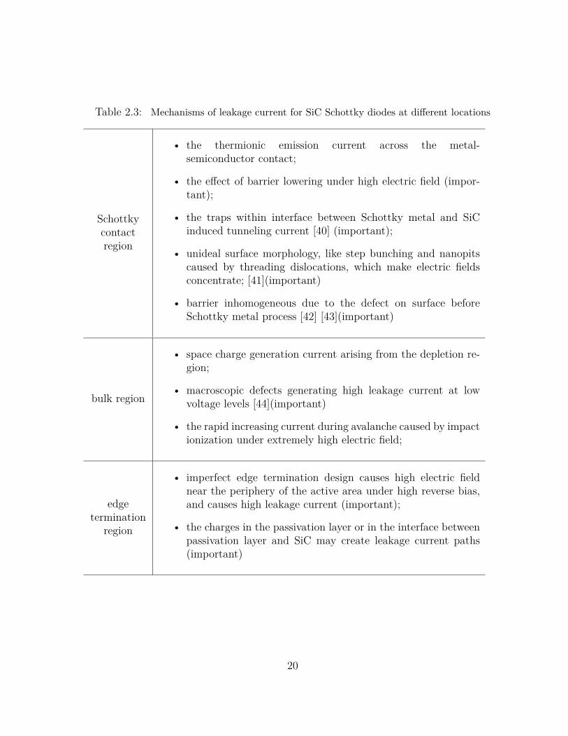
Table 2.3: Mechanisms of leakage current for SiC Schottky diodes at different locations
Schottkycontactregion
• the thermionic emission current across the metal-semiconductor contact;
• the effect of barrier lowering under high electric field (impor-tant);
• the traps within interface between Schottky metal and SiCinduced tunneling current [40] (important);
• unideal surface morphology, like step bunching and nanopitscaused by threading dislocations, which make electric fieldsconcentrate; [41](important)
• barrier inhomogeneous due to the defect on surface beforeSchottky metal process [42] [43](important)
bulk region
• space charge generation current arising from the depletion re-gion;
• macroscopic defects generating high leakage current at lowvoltage levels [44](important)
• the rapid increasing current during avalanche caused by impactionization under extremely high electric field;
edgetermination
region
• imperfect edge termination design causes high electric fieldnear the periphery of the active area under high reverse bias,and causes high leakage current (important);
• the charges in the passivation layer or in the interface betweenpassivation layer and SiC may create leakage current paths(important)
20

diode turn-off performance is shown, while all the other parameters keep unchanging.
The voltage and current across the diode is shown in Figure 2.4. The diode is turning
off at 400V, 43.7A. We can see that the di/dt of the diode during turn-off does not
change with increased junction capacitance, while the voltage curve has a slight change.
The dV/dt is approximately 14.5V/nsec, and the di/dt is 593 A/usec. The peak reverse
recovery current (Vrrm) and reverse recovery charge (Qrr) is compared in table 2.4. The
diode with higher junction capacitance shows higher peak reverse current and thus higher
switching losses. In some actual applications, the diodes are parallel to the MOSFETs,
and the diode capacitance will add to the MOSFET output capacitance Coss and cause
higher switching losses.
Figure 2.3: simplified circuit dia-gram of double pulse test in LTspice
3 . 0 0 x 1 0 - 6 3 . 0 4 x 1 0 - 6 3 . 0 8 x 1 0 - 6 3 . 1 2 x 1 0 - 6 3 . 1 6 x 1 0 - 6 3 . 2 0 x 1 0 - 6
0
2 0
4 0
6 0
8 0 u s i n g s t a n d a r d d i o d e m o d e l u s i n g d i o d e m o d e l w i t h d o u b l e d j u n c t i o n c a p a c i t a n c e
T i m e ( s e c )
Diode
Curre
nt (A)
0
1 0 0
2 0 0
3 0 0
4 0 0
Diod
e Volt
age (
V)Figure 2.4: diode turn-off waveforms withstandard model and model with two timesjunction capacitance
For the bipolar diode, it will have larger reverse recovery loss due to stored carriers
within the drift region when at on state, and to remove the stored carriers, a larger
reverse current is needed, thus causing higher reverse recovery loss. For high voltage
21

Table 2.4: comparison of parameters of diode reverse recovery
Irrm(A) Qrr(nC)original model 3.0 58.7
model with twice Cj 4.9 114.8
SiC bipolar diode with low injection efficiency, it still causes larger reverse recovery loss
compared to JBS diode. One example is that the body diode of the SiC MOSFET shows
larger reverse recovery loss than JBS diode [45]. Mixed-mode simulation was conducted in
Sentaurus TCAD, and a 10 kV SiC MPS diode was turned off under 1 kV, 100 A/cm2. The
reverse recovery curve is shown in Figure 2.5. The distribution of minority carrers during
switching period suggested by the dash line in Figure 2.5 was shown in Figure 2.6. For the
10 kV silicon carbide MPS diodes, the injection efficiency is low with the ion implanted
p-type region, so the carrier concentration is low close to the anode, so in this case when
current drops to zero, the minority carriers at the boundary of the P-n- junction already
drops to zero. When current continues to reduce to extract the stored carriers, the drift
region starts to be depleted, and electric field starts to increase in the depletion region,
so that the reverse voltage of the diode starts rising. When the voltage reached to the
desired point, there are still stored charges inside the drift region needs to be removed,
leading to a long tail the current waveform at the end of the reverse recovery phase. This
simulation result was also similar to the measured performance shown in Figure 4.36.
While for the SiC PiN diodes, it has higher minority concentration close to the anode,
if comparing the MPS diode reverse recovery performance with the same voltage rating.
There would be more carriers at the boundary when current is reducing to zero and
reversed. In that case a longer reverse recovery time is needed for extracting the carriers,
and the higher peak reverse recovery current will also be induced.
22

At the n-N+ junction side, at this case there are higher concentration of minority
carrier close to cathode, which is beneficial to its performance. If there are not enough
minority carrier concentration close to cathode, or the carrier lifetime at that region is
too low, it will induce a case that at some point there will only be stored carriers in
the middle of the drift region, and there is no source of reverse current because of no
difference of carriers between the two junctions. The reverse current will instantly go to
zero, which shows a snappy behavior. It can be detrimental to the system as it causes
high di/dt and oscillations. A smooth waveform is always favored in real applications.
Figure 2.5: Mixed-mode simulation of the reverse recovery performance of 10 kV SiCMPS diodes
Discussions on the reverse recovery process of the high voltage silicon carbide bipo-
lar devices have been limited for several reasons. One is that the experimental study of
23

Figure 2.6: Distribution of minority carriers within the drift region under the middle ofSchottky contact when voltage starts to rise
comparison of ultra-high voltage diode reverse recovery performance is limited due to the
unavailability of different types of high voltage diodes with robust package withstanding
ultra-high voltage. The construction of power circuit with ultra-high voltage and fast
transient is also a challenge; Second is that for numerical simulations, it requires accu-
rate parameters inside the p-type emitter (localized electron/hole lifetimes and mobility)
to have simulation results close to experimental ones, but these parameters cannot be
acquired directly with characterizations and is largely depend on the process. The tradi-
tional analytical derivation of the reverse recovery process for power diodes also does not
apply to this extreme case, due to low-level injection, less than unity injection efficiency,
etc, which has been analyzed formerly [2].
24

2.2.4 Surge Performance
The surge robustness of high voltage diodes are commonly required in high power appli-
cations. Table 2.5 listed several commercially available high power silicon diodes (>5 kV,
200A) and their non-repetitive surge current capability. Most of the diodes were silicon in
wafer with press-pack package, except ABB 5SLD0600J650100, which is packaged with
diced chips within a power module, which shows inferior surge capability compared to
press-pack devices.
Table 2.5: comparison of surge capability between various commercial high power silicondiodes
CompanyProduct No
VoltageRat-ing/V
CurrentRatingIF (AV )M
/A
SurgeCurrentRatingIFSM /A
Surge Test ConditionRatio
(IFSM/IF (AV )M)
ABB5SDD06D6000 6000 662 10.5k Non-Repetitive 10ms,
150C 15.9
ABB5SDD50N6000 6000 4.21k 71.2k Non-Repetitive 10ms,
150C 16.9
ABB5SDF02D6002 6000 250 3.6k/11.4k Non-Repetitive 10ms/1ms,
125C 14.4
ABB5SDF10H6004 6000 1100 18k/44k Non-Repetitive 10ms/1ms,
125C 18.0
ABB5SLD0600J650100(Module)
6500 600 6k Non-Repetitive 10ms,125C 10.0
InfineonD471N90T 9000 565 10k Non-Repetitive 10ms,
160C 17.7
InfineonD2601N90T 9000 2.24k 50k Non-Repetitive 10ms,
160C 22.3
Current studies about surge capability of silicon carbide Schottky diodes are lim-
25

ited under low voltage(1200V). Both the simulation and experimental studies have been
carried out [46]. There are still little study of the surge capability of the high voltage
device, mainly due the immature device technology and no commercial devices available.
Nevertheless, the principle of the surge performance is quite similar. For better surge
capability, the MPS structure is applied to have a lower differential resistance at high
current and high temperature.There are several factors which will determine the surge
capability of the device, which will be explained as follows.
The first factor is the process parameters of forming the p-type region. As stated in
Section 2.2.1, the process of forming the p-type region determines the injection efficiency,
which determines the differential resistance when MPS diodes are working in the bipolar
region. There have been studies showing that, by conducting Al ion implantation at high
temperature of 500C, the devices show superior surge capability compared to devices
with ion implantation at room temperature [47]. According to authors, the reason may
be the Ohmic contact formed directly to the as-deposited Ti and the ion implanted p-
type region with the high temperature implantation step. Another reason is the wide p+
transition region, which will also be discussed in the next paragraph. There have been
studies on forming the p-type region by epitaxial growth on trenches [48], but the surge
capability has not been discussed on diodes made using these methods.
The second factor is the geometry design of the active cell. The width of the Schottky
contact will determine its forward behavior and therefore also determine the surge per-
formance, as discussed in the previous sections. Other than that, the width of the p-type
region will also have a great impact. TCAD simulation is conducted on analyzing the ef-
fect of the width of p-type region on the forward current-voltage (IV) characteristics. The
basic structure is based on Figure 2.1 (b), with half-cell width of the Schottky contact
Ws=3 µm. The drift region has thickness of 99 µm and doping concentration of 2.66e14
26
cm−3, which is for blocking around 10 kV, which is also consistent with the wafer for fab-
rication in the following chapters. The Schottky barrier height is set as 1.7 eV, also to be
consistent with further experiment results. The p-type region has impurity concentration
of 1e20 cm−3. To simulate the forward characteristics, the Ohmic contact and Schottky
contact should be defined separately, and the transient simulation in circuit should be
conducted to catch the possible snap-back phenomena. The forward characteristics is
shown in Figure 2.7. In unipolar region, with increasing the width of p-type region, the
differential resistance was decreased slightly, due to the narrower current paths. But for
high voltage device with a thick drift region, the variation of the current path close to the
surface does not have a big effect on the total resistance. When temperature goes higher,
the unipolar device has larger differential resistance due to decreased mobility. When Wo
increases, the voltage at when the device shifts from unipolar region to bipolar region,
which is defined Vturnon, decreases significantly. This is because when Wo increases, the
potential difference between the middle of the p-type region and the n-type drift region
can reach the built-in potential (Vbi) at lower forward voltages to turn on the pn junction.
At higher temperature of 473K, Vturnon decreases slightly due to the decreased built-in
potential of the pn junction. The snapback phenomenon reveals at lower Wo, and when
Wo increases, the snapback phenomenon disappears due to lower Vturnon .
The performance of diodes under surge current is also simulated for further com-
parison. In that case a electro-thermal simulation is conducted in Sentaurus TCAD.
Device is modeled with low thermal resistance attached to the bottom representing the
behavior of a heatsink. A sinusoidal current waveform with peak current of 1000 A/cm2
and duration of 10 msec is applied. The environment temperature is set as 300K and
473K. The voltage and temperature versus time is shown in Figure 2.8 and Figure 2.9.
The snapback phenomenon can still be seen with Wo=2 µm when the current is rising
27

Figure 2.7: forward characteristics of the high voltage JBS/MPS diodes with varyingWo at (a) 300K (b) 473K
and falling. When Wo increases, the less voltage drop will be across the device, and the
temperature increase will be less significant. It can be seen that a difference of around
50 K will happen between the highest temperature of diodes of Wo=2 µm and Wo=11
µm. The similar big difference was shown with environment temperature of 473 K. The
difference can also be influenced by the actual device package and its thermal network
with respect to the environment, and the simulation may need more calibration in the
future for describing the real situations.
Another parameter to evaluate is the coverage width of the contact. A long p-type
region can often be seen at the transition region between the active area and edge termi-
nation regions. The metal contact does not cover all the p-type regions on the edge, as
part of the p-type region functions as the edge termination to alleviate high electric field
near the edge. The device structure with a long p-type region (Wo=12 µm, Ws=2 µm)
is simulated, with one structure of contact covering all the surface, and another covering
only small part of the p-type region connecting to Schottky contact. The forward char-
acteristics in shown in Figure 2.10. It can be seen that the less contact coverage only
makes the forward characteristic marginally worse at 300K, and at 473 K the difference
28

(a) (b)
Figure 2.8: the voltage and temperature waveform of diodes with various Wo at 300K
(a) (b)
Figure 2.9: the voltage and temperature waveform of diodes with various Wo at 473K
29

is small enough to be neglected. The hole current density at 473 K , 200 A/cm2 is also
seen in Figure 2.11. Despite the increased current density close to the surface in p-type
region due to the narrow contact and current concentrating under it. The rest parts of
the device almost have the same distribution of currents.
Figure 2.10: forward characteristics of the high voltage JBS/MPS diodes with wide andnarrow contact coverage at 300K and 473K
The third factor that determines the surge capability is the wire bonding and pack-
aging technology. Usually the failure happens on the metallization layer or or around
the wire bonding pad. By using advanced metallization and wire bonding technologies
(Like Cu metalization [49] and heavy Cu wire bonding [50]), the device can have higher
thermal conductivity, thus being able to withstand higher surge energy.
More discussion about designing active area layout of high voltage SiC MPS diodes
on improving surge capability will be demonstrated in Chapter 4.
30

Figure 2.11: hole current density close to the top surface of the 10 kV SiC MPS diodeswith (a) wide (b) narrow contact
(a) (b)
Figure 2.12: the voltage and temperature waveform of diodes with wide and narrowOhmic contact at surge condition at 300 K and 473 K
31

2.2.5 di/dt Capability
In power electronics applications, devices are required to be switched at a faster rate
to reduce switching time and loss. Sometimes device may experience extreme conditions
and being switched at a faster rate than normal conditions. This trend requires diode
to be able to have higher di/dt and dv/dt capability. One of the well known limiting
factor of di/dt capability is that due to high di/dt, the device may have higher peak
reverse recovery current, when the device was usually supporting the reverse voltage at
the same time. In this case, the reverse current will increase the electric field compared
to static case, thus cause device to breakdown at values lower than BV, which is also
called dynamic breakdown [40]. There have been many studies previously on silicon power
diodes to improve its dynamic breakdown, or reverse recovery safe operating area(SOA)
capability, but much less study has been presented in silicon carbide. The principles of
increasing the reverse recovery SOA is similar regardless of silicon or silicon carbide.
One method is that by reducing the stored carrier concentration close to anode at on-
state, the device will need less time in reducing charges when diode current is decreasing,
so that the peak reverse recovery current can be reduced. In that case, potentially the
MPS structure will have a higher di/dt capability compared to PiN at the same voltage
ratings [2,40]. The comparison of carrier concentration between MPS diode and PiN will
be presented in Chapter 3. In silicon world, there have also been many engineering on
the n/n+ junction, which proves to be the key in determine the reverse recovery SOA
and softness of the diode [51, 52], also the transition region between the active area and
edge termination may also take a part in determine the di/dt capability [53], but they
have not been discussed in silicon carbide yet.
32

Chapter 3
High Temperature Characterization
of 10-kV SiC MPS Diodes
3.1 Device Structure
The 10 kV MPS diodes have been previously designed in FREEDM and fabricated in
CREE [2]. The wafer was initially subjected to thermal oxidation to enhance the lifetime
from medium value of 1 µsec to around 2 µsec . Floating field rings were used as the
edge termination technique, and P+ ion implantation was done with aluminum ions at
high temperature (600C) followed by high temperature activation anneal to form both
the anode and the floating filed rings. Nickel was deposited on the backside to form the
Ohmic contact followed by RTA. Nickel was deposited on the front side to form both the
Schottky contact on the N- drift region and Ohmic contacts to the P+ regions. The PiN,
MPS, JBS structure is fabricated on the same wafer, with drift layer doping concentration
of 2.7 x 1014 cm−3 and thickness of 100 µm. The cross section is the same as shown in
Figure 2.1. For MPS diodes, Wo is 1 µm and Ws is 0.5 µm. For JBS diodes Wo is 0.5
33
µm and Ws is 2 µm. Devices with active area of 0.10 cm2 are diced and packaged for
characterization.
3.2 Forward Characteristics
For testing the forward characteristics of the power diode, Tektronix 371A curve tracer
was used, which is one of the most common tool for characterization of power devices. A
hot plate was attached to the bottom of packaged device, with thermal paste in between to
reduce the thermal resistance. The single pulsed mode was used to limit the self-heating of
the device at on-state. All the rectifiers were characterized from room temperature to 200C. The forward i-v characteristics of the diodes are shown in Figure 3.1(a). The forward
characteristics of the MPS and PiN rectifiers are very close both at room temperature
and high temperature because of minority carrier injection into the drift region. The JBS
diode shows unipolar behavior at room temperature with a high on-state voltage drop
compared to the PiN and MPS rectifiers. The on-state voltage drop for the JBS rectifier
decrease at 200 C because it behaves like the MPS rectifier at higher current densities.
Figure 3.1(b) shows the forward voltage drop at 20 A/cm2 versus temperature with
different types of devices. For the JBS diode, the forward voltage drop increases up to
100 C because the drift region resistance increases. It is due to the lattice scattering effect
at high temperature, which reduced the electron mobility. When temperature exceeds 100C, the built-in potential of the P+/N junction decreases sufficiently to allow injection
into the drift region. The JBS diode then begins to behave like the MPS rectifier, and the
voltage drop and differential on-state resistance keeps decreasing at higher temperature.
For the PiN diode, the forward voltage drop keeps decreasing, which shows that the
minority carrier injection dominates the device behavior, and higher temperature results
34

in higher carrier lifetime, and makes the differential on-state resistance lower.
Figure 3.1: Measured forward I-V of the PiN JBS and MPS at room temperature andhigh temperature (200 C)
3.3 Reverse Bias Leakage Current Characteristics
The reverse bias characteristics of the packaged diodes at room temperature and 125 C
are shown in Figure 3.3. The leakage current for all the devices increases by two orders of
magnitude at a reverse bias voltage of 4 kV. The leakage current for the JBS diodes is the
largest due to the large area of the Schottky contact. It has much larger leakage current
compared to MPS diodes because of wider spaces between the P+ regions resulting in
higher electric field at the Schottky contact. One MPS diode was characterized up to 8 kV
with temperature up to 200 oC with the package provided by Cree [2], and it is the device
35

Figure 3.2: Forward voltage drop of the PiN, JBS and MPS diodes at 20A/cm2
with the lowest leakage current and highest blocking capability at high temperature as
shown in Figure 3.4 with all different kinds of devices tested so far.
The leakage current for the MPS rectifier is lower than that observed for the PiN
diode. One possible explanation is that ion implantation of the P+ anode region in the
P-i-N diode introduces defects that act as generation centers near the anode junction.
The low leakage current observed in the MPS diode indicates that the narrow space
between its P+ regions effectively shields the electric field at the Schottky contact.
Another phenomenon when testing devices is that it shows instability in terms of
increase leakage current after multiple times of testing. Several PiN dies were selected for
the reverse bias test. The die was immersed in flourinert (FC-40 from 3M corporation),
and connected with a high voltage source(up to 30 kV) and a large resistor to limit the
current [2]. The diode was tested up to 5 kV with leakage current compliance level of
1 µA. For testing, the device experience increase of reverse voltage of 100 V every one
second up to 5 kV, and there are at least one minute gap between each test. No significant
36

Figure 3.3: Measured reverse I-V of the PiN JBS and MPS diode at room temperatureand 125 C
Figure 3.4: Measured reverse I-V of the MPS diode from room temperature to 200 C
37

degradation of leakage current is shown in Figure 3.5, but the result is not quite uniform.
Sometimes the leakage current did not increase monotonically, partly because of the test
system generating some capacitive current, or may due to the dynamic charges inside
the edge termination region, which redistribute the electric field from time to time and
cause shifting of leakage current. The PiN diode was also heated up to 75 C and 125 C
and tested multiple times up to 5 kV in Figure 3.6. At 75 C, the device shows similar
behavior compared to results at room temperature, and at 125 C, a clear trend of leakage
current increasing exponentially with voltage is shown, and it increased after multiple
tests. If it is charges in edge termination region causing the unideal shifting of the leakage
current at room temperature, it seems at 125 C these charges may move quickly and
does not cause main portion of the leakage current, and it is mostly likely resulted from
the implanted p-n junction at 125 C, which is degrading after stress.
Figure 3.5: Multiple time measurement of reverse I-V of the PiN diode die at roomtemperature
38

(a) (b)
Figure 3.6: Multiple time measurement of reverse I-V of the PiN diode die at (a) 75 Cand (b) 125 C
3.4 Reverse Recovery Characteristics
Double-pulse test was conducted to measure the reverse recovery behavior of the diodes
at elevated temperatures. The test setup picture is shown in Figure 3.7. A high voltage
SiC MOSFET was used as the active switch, and the diode was mounted on a hot plate
for high temperature measurements. The elements were being as close as each other, to
minimize the parasitics, like inductance in the gate loop and power loop. The duration
of the first pulse was adjusted to provide an on-state current of 1 A before being turned
off, and the bus voltage is 1 kV.
The reverse recovery current waveform is shown at various temperatures in Figure 3.8
for the MPS and PiN rectifier. The PiN rectifier has much larger (around 1.5x) peak
reverse current and Qrr at room temperature. The difference becomes greater with in-
creasing temperature. One big difference of the curves is that, for MPS diode, when the
current is decreasing and became reversed, the di/dt was constant at first but decreased
afterwards. At first, di/dt is determined by the gate resistance of the SiC MOSFET for
turning on the switch at the second pulse and the voltage across it when turning off the
39

Figure 3.7: Test Set-up for measurement of reverse recovery
diode, which is VDC . When the charge starts to be extracted, the depletion region was
formed and voltage being supported, at that time, the voltage across the parasitic induc-
tance Ls drops and thus di/dt decreases. However, this phenomenon was not discovered
in the PiN diode in the same circuit. That is because for PiN diode, there is more stored
charge close to anode, and when current is decreasing and reversed, the stored charge
close to anode can not be fully removed, and depletion region cannot be supported. In
that case, the voltage across Ls keeps constant, so di/dt was also constant. Measured
reverse recovery charge versus the temperature is shown in Figure 3.9. It shows that the
difference in terms of reverse recovery charge is small at room temperature between PiN
and MPS, but at higher temperature, MPS diode shows much lower reverse recovery
charge compared to PiN diode. The trade-off curve between forward voltage drop and
reverse recovery charge is shown in Figure 3.10. It can be seen that the trade-off curve
becomes more favorable for the MPS rectifier compared with the PiN rectifier when the
temperature is increased from 25 C to 200 C.
40

(a) (b)
Figure 3.8: The reverse recovery waveform of SiC (a) MPS (b) diode at different tem-perature
Figure 3.9: Measured reverse recovery charge of PiN and MPS diodes.
41

Figure 3.10: The Trade-off Curve Between Reverse Recovery Charge and Forward Volt-age of SiC PiN and MPS diode at different temperature(C)
3.5 Device Analysis
Numerical simulations were conducted to compare the performance of the 10 kV PiN and
MPS rectifiers at different temperatures using TCAD Sentaurus. The lateral spreading
of the P+ region [54] was considered in device simulation because it has a significant
impact for the MPS diodes with the narrow gap between the P+ regions under the
Schottky contact. The P+ region dose was defined by Pearson functions [1] based on the
actual ion-implantation energy and doses used in the fabrication.
The minority carrier lifetime in the starting wafer, measured by the microwave pho-
toconductive decay (µPCD) method, was found to be 2 µsec after lifetime enhancement.
Ion implantation creates the lifetime killing defects at the junction. So that the effective
lifetime in the ion implanted region was lower than the lifetime in the bulk epi layer,
and this value is sensitive to the process parameter of the ion implantation, and really
determines the performance. Figure 3.11. The parameters in the simulation, like drift
42

region parameters, Schottky contact was set as close as possible to the device behavior.
The local lifetime value was set as 0.1 nsec for the PiN diodes and 0.2 nsec for the MPS
diodes, so that they have a very similar forward characteristics both at room temperature
and 200 C, which is similar to the characterization result, as shown in Figure 3.12. The
characterization result shows higher forward voltage drop, which may result from the
lower local lifetime values.
Figure 3.11: Forward IV of the MPS diode with different local lifetime in the ion im-plantation region
The injected carrier distribution in the PiN and MPS diodes are shown in Figure 3.13
at the same on-state current density of 10 A/cm2. The PiN diode has the expected
centenary carrier distribution [16]. The carrier density is much lower at the upper surface
as expected for the MPS rectifier, which caused different reverse recovery behavior. In
both cases, the injected carrier concentration increases when the temperature is raised to
200 C. The enhanced conductivity modulation of the drift region in both diodes produces
43

Figure 3.12: Forward IV of the MPS and PiN diodes though numerical simulation atroom temperature and 200 C
a reduction in the on-state voltage drop as observed in Figure 3.2 and Figure 3.14. At
the same current density, the MPS diode has less stored charge compared to PiN diode,
because there are part of the current going through the Schottky contact and does not
contribute to the stored charge.
From Figure 3.13, it can be concluded that the stored charge within the drift region
for the MPS rectifier is much smaller than in the PiN rectifier. This stored charge in
the drift region must be removed during the reverse recovery transient. The smaller
stored charge in the MPS rectifier produces the smaller reverse recovery current observed
in Figure 3.8. The stored charge in the diodes can be extracted by integration of the
carrier profile in the drift region across the thickness. The stored charge obtained from
the numerical simulations is shown in Figure 3.14 for various temperatures. The stored
charge in the on-state increases for both diodes with a greater increase observed for the
PiN diode. This is good agreement with the measured increase in reverse recovery charge
44

Figure 3.13: Minority carrier concentration in the drift region of PiN and MPS at 25 Cand 200 C for an on-state current density of 10 A/cm2
with temperature as shown in Figure 3.9.
45

Figure 3.14: Stored charge of PiN and MPS diodes at 10A/cm2 from numerical simula-tion at different temperatures
46

Chapter 4
Design, Fabrication and
Characterization of 10-kV SiC MPS
Diodes with High Schottky Barrier
Height
4.1 Device Design
4.1.1 Aluminum Ion Implantation
Ion implantation is currently the most common method for selective doping in silicon
carbide (SiC), and analytical method using Pearson function has been commonly used
for calculating the vertical doping concentration profile [1]. Recently, Monte Carlo (MC)
simulation based on Binary Collision Approximation has been demonstrated to have a
more accurate profile, especially at low background doping level compared to analytical
47

approximation like the Pearson method [55]. The multiple Al ion implant was conducted
to form the P region in active area and the floating field rings, with dose of 5× 10¹⁴/1×
1015/2 × 1015/1 × 1014 cm-2, and energy of 30/70/140/300 keV at 600 C. Figure 4.1
shows the comparison of the one dimensional Al impurity concentration profile at vertical
direction by Pearson Function [1] and the MC simulation results with the implantation
schedule. In MC simulation, the 4 degree off-axis substrate is defined to represent the
normal condition. Over 1 × 10⁶ ion trajectories were used for MC simulation to ensure
the accuracy of the profile. Monotonically decreasing Al concentration is observed in
Figure 4.1. These two profiles match well at doping concentrations over 2 × 1016 cm-3,
but below that, the MC simulation result shows longer tail, and has 0.61 µm deeper
junction depth at doping level of 3× 1014 cm-3 compared to Pearson function results.
0.0 0.2 0.4 0.6 0.8 1.0 1.2 1.4 1.6 1.8 2.01E14
1E15
1E16
1E17
1E18
1E19
1E20
Alum
inum
Con
cent
ratio
n (c
m-3)
Depth (um)
Pearson Function Sentaurus MC
0.61 m
Figure 4.1: Comparison between Pearson Function [1] and Monte Carlo Simulation ofAl impurity concentration profile at vertical direction
48

Compared with vertical profile, the lateral straggling of Al ion implant into silicon car-
bide has not been fully investigated. Previous studies [54,56,57] claimed that the lateral
straggling of Al in 4H-SiC would have a significant impact on the device performance,
like the forward I-V of JBS diodes. However, few studies have been found on devices
with background doping concentration lower than 1× 1015 cm-3 for breakdown voltages
of higher than 10 kV. The tail of the Al concentration profile is deeper on devices with
lower background drift region doping concentration, thus affecting device performance.
To calibrate the 2D dopant profile, the techniques of scanning probe microscopy
(SPM), like Kelvin Probe Force Microscopy (KPFM), Scanning Capacitance Force Mi-
croscopy (SCFM) and Scanning Spreading Resistance Microscopy (SSRM) are most used
[58–60]. Other than that, the Secondary Electron Potential Contract (SEPC) method was
also developed as an effective method for 2D dopant imaging in SiC [61]. It basically arises
from the potential contrast due to built-in potential, which produces a stray electric field
irradiating from the surface of the semiconductor sample. This method favors the wide
bandgap material like silicon carbide, which has higher built-in potential and can produce
stronger electric field to accelerate or retard the low energy secondary electrons. A fabri-
cated Junction Barrier Schottky (JBS) diode [62] was cleaved and put into the chamber
of FEI Verios 460L field-emission scanning electron microscope (FESEM) from Analytical
Instrumentation Facility (AIF) in North Carolina State University. Figure 4.2 shows the
image across the active cell area and the edge termination region of the SiC JBS diode
with background doping concentration of 8e14 cm-3. It has the edge termination design
of multiple floating field rings (FFR) on the right hand side of the image and breakdown
voltage of >10 kV. The multiple Al ion implant was conducted to form the P region both
in active area and the floating field rings, with dose of 5×10¹⁴/1×1015/2×1015/1×1014
cm-2, and energy of 30/70/140/300 keV at 600 C. The full-cell width is 5 µm with Ohmic
49

contact width of 1 µm on mask. From this SEM image, the lateral spreading width of the
Al is approximately 0.5 µm on each side. Unlike the original study [61], the exact profile
of doping concentration was not able to be extracted accurately by the contrast, which
may result from different detectors and samples’ surface conditions. Anyway, the lateral
straggling effect is significant enough to affect the device performance of JBS diodes with
edge terminations.
Figure 4.2: SEM image of the fabricated 10 kV SiC JBS diode with drift region dopingof 8× 1014 cm-3
The Monte Carlo simulation was also carried out in Sentaurus TCAD. The two-
dimensional aluminum active doping concentration is shown in Figure 4.3. The total
dose of the ion implantation is 3.6 × 1015 cm-2 as mentioned above for (a) and 2 × 10¹³
cm-2 for (b). The lateral Al active concentration contour depends on the total dose, and
even with dose of 2× 1013 cm-2, a lateral spreading of 0.5 µm was found due to the low
background doping concentration. It shows stronger lateral straggling effect compared to
50

the SEPC result. Currently, both methods are still under evaluation of the accuracy, but
at least it shows that the lateral straggling effect are unnegligible.
1e13
1e14
1e15
1e16
1e17
1e19
1e13
1e14
1e15
1e161e17
1e18
1e13
1e14
1e15
1e161e17
1e18
1e13
1e14
1e15
1e16
1e17
1e19
1e13
1e14
1e15
1e161e17
1e18
Oxide Oxide
(a) (b)
Figure 4.3: Al active concentration contour with oxide mask (a) total dose of 3.6× 10¹⁵
cm-2(b) total dose of 2× 1013 cm-2
4.1.2 Basic Cell Design
The parameters of the basic half-cell structure determine the performance of the diodes.
They include the width of the p-type region with Ohmic contact (Wo), the width of the
Schottky contact (Ws), the depth of the p-type region (the aluminum ion implantation
schedule), and the Schottky barrier height (SBH). The effect of the Wo barely influenced
the performance in the unipolar region at 10 kV level, which has been discussed in
Chapter 2. The aluminum doping concentration by ion implantation is typically required
to be high and constant close to the top. A deep p-type region is also usually favored
to shield the electric field effectively at reverse bias, but the dose and the energy is
usually limited by the equipment and cost in manufacturing. They are chosen as dose of
5× 10¹⁴/1× 1015/2× 1015/1× 1014 cm-2, and energy of 30/70/140/300 keV at 600 C, as
51

shown above, which has been proved effective in fabricating MPS diodes [2]. The width
of the Schottky contact Ws is the most important parameter and has been discussed
extensively [16]. However, one features has to be stressed. When Ws is 0.5 µm or even
smaller, the region under the Schottky contact will be depleted under forward bias, which
forms a pinched barrier. It will increase the knee voltage of the diode. On the other hand,
it will have a benefit on injection from the p-type area at lower forward voltages. It is
needed for high voltage MPS diodes, as the potential difference near the pn junction on
top has a small fraction of the total on-state forward voltage with most on the thick drift
layer. Furthermore, the higher SBH also helps reduce the leakage current at reverse bias
condition [2].
0 1 2 3 4 5 60
5
10
15
20
25
30
35
40
45
50
Cur
rent
Den
sity
(A/c
m2 )
Forward Voltage (V)
SBH=1.0 eV SBH=1.3 eV SBH=1.6 eV
Figure 4.4: Forward characteristics of 10 kV SBD with different Schottky barrier heightat room temperature
The forward behavior of 10 kV diodes with different SBH was simulated in Sentaurus
52
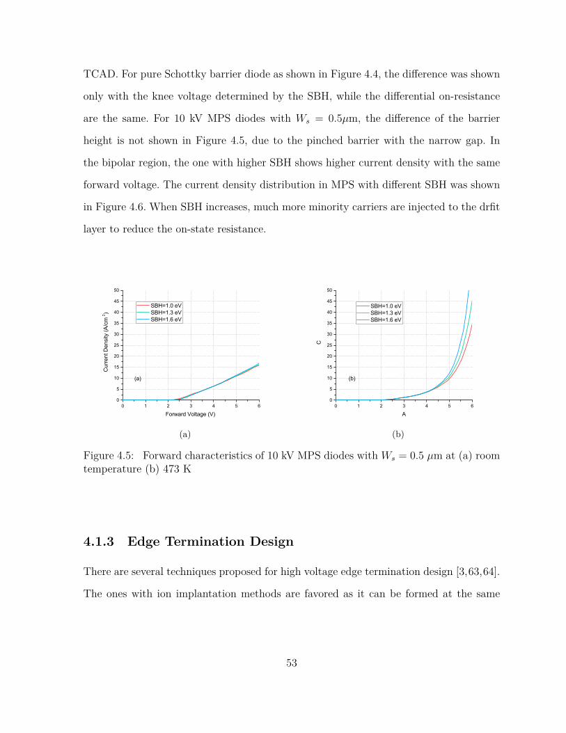
TCAD. For pure Schottky barrier diode as shown in Figure 4.4, the difference was shown
only with the knee voltage determined by the SBH, while the differential on-resistance
are the same. For 10 kV MPS diodes with Ws = 0.5µm, the difference of the barrier
height is not shown in Figure 4.5, due to the pinched barrier with the narrow gap. In
the bipolar region, the one with higher SBH shows higher current density with the same
forward voltage. The current density distribution in MPS with different SBH was shown
in Figure 4.6. When SBH increases, much more minority carriers are injected to the drfit
layer to reduce the on-state resistance.
0 1 2 3 4 5 60
5
10
15
20
25
30
35
40
45
50
Cur
rent
Den
sity
(A/c
m2 )
Forward Voltage (V)
SBH=1.0 eV SBH=1.3 eV SBH=1.6 eV
(a)
(a)
0 1 2 3 4 5 60
5
10
15
20
25
30
35
40
45
50
(b)
C
A
SBH=1.0 eV SBH=1.3 eV SBH=1.6 eV
(b)
Figure 4.5: Forward characteristics of 10 kV MPS diodes with Ws = 0.5 µm at (a) roomtemperature (b) 473 K
4.1.3 Edge Termination Design
There are several techniques proposed for high voltage edge termination design [3,63,64].
The ones with ion implantation methods are favored as it can be formed at the same
53

(a) (b)
Figure 4.6: Current densities of MPS diodes at Vf = 6V with Schottky barrier height of(a) 1.0 eV and (b) 1.6 eV at 473 K
time with active area for MPS diodes, and do not need extra etch and epitaxial steps.
Previous works in FREEDM has utilized structure of multi-floating field rings (FFRs),
and only one heavily dosed ion implantation step is needed. It has total of 100 rings of
4 µm width and gradually increasing space starting at 1 µm [2]. The space is increasing
with the trend as shown below:
Sn = S1 + ((n− 1)Si)2 (4.1)
Where Sn means the space width between the (N-1)th ring and the Nth ring, and
S1=1 µm, n=100.
An extra one step of nitrogen ion implantation step is always needed to form a heavily
doped n-type region outside the last edge termination ring and close to the edge of the
chip, which is also called the channel stop region, to stop electric field from extending to
54

the edge of the chip and cause reliability problems. Because of the narrow starting space
of 1 µm, the effect of lateral straggling has to be considered. The cross-section profile
close to the anode obtained from MC simulation is shown in Figure 4.7. Due to the lateral
straggling, the rings from 0 to 200 µm from the active area were merged together. An
SEM image was also taken for the fabricated device with the same parameters [2], which
shows the similar results in Figure 4.9.
Figure 4.7: Simulation structureclose to the anode for FFR edgetermination (a) without and (b) withincluding lateral straggling effect
Figure 4.8: Schematic illustration ofthree kinds of edge termination for 10kV device (a) multiple FFR (b) MFZ-JTE (c) Hybrid JTE
The electric field distributions along the edge termination for profiles with and without
lateral straggling are shown in Figure 4.10 and Figure 4.11. The merging of the first
multiple rings caused the reverse voltage mainly supported by the rings far from the
anode, resulting in high electric field close to the last ring. The larger amount of positive
interface charge leads to increasing electric field close to the anode, and decreasing field
at locations far from anode.
There are another two types of edge termination design proposed, which is multiple-
floating-zone junction termination extension (MFZ-JTE) [3] and hybrid junction termi-
55

Figure 4.9: SEM image of the edge termination area of the fabricated 10 kV SiC JBSdiode with drift region doping of 8× 1014 cm-3
0 100 200 300 400 500 600 700 8000.0
5.0x10⁵
1.0x10⁶
1.5x10⁶
2.0x10⁶
2.5x10⁶
3.0x10⁶
Elec
tric
Fiel
d (V
/cm
)
Distance from the Anode (um)
Charge Density = -1e12 cm -2
No Interface Charge Charge Density = 1e12 cm -2
Figure 4.10: Comparison of the elec-tric field distribution along the FFRedge termination (y=0.3) at 10 kVwith different interface charges with-out lateral straggling
0 200 400 600 8000.0
5.0x10⁵
1.0x10⁶
1.5x10⁶
2.0x10⁶
2.5x10⁶
3.0x10⁶
Elec
tric
Fiel
d (V
/cm
)
Distance from the Anode (um)
Charge Density = -1e12 cm -2
No Interface Charge Charge Density = 1e12 cm -2
Figure 4.11: Comparison of the elec-tric field distribution along the FFRedge termination (y=0.3) at 10 kVwith different interface charges withlateral straggling
56

nation extension (Hybrid-JTE) [63], and illustrated in Figure 4.8. For MFZ-JTE, the
width of the junction termination rings were decreased using Wn = Wn−1/1.02, where
n = 36,W1 = 12.5 µm with a total width of 450 µm. Figure 4.12 shows the simulated
breakdown voltage with different interface charges. The FFR structure shows large varia-
tion of breakdown voltage against charges, and it has opposite impact for structures with
and without lateral straggling. This can be explained by the electric field distribution in
Figure 4.10 and Figure 4.11. For structures without lateral straggling, high electric field
appears near the anode, and more positive charges will further increase the electric field
near the anode, thus decreasing the breakdown voltage. While for structures with lateral
straggling, more positive charge will relieve the highest electric field near the edge, thus
increasing the breakdown voltage. Compared to the FFR design, MFZ-JTE was much
less sensitive to interface charges, and also the difference between structures with and
without lateral straggling is small, which may be due to the weak lateral straggling effect
with low dose implantation. Hybrid-JTE also shows low level of sensitivity against inter-
face charges when not considering the lateral straggling effect, but the negative interface
charges seem to affect its breakdown voltage when including the lateral straggling effect.
Overall, the lateral straggling has a big impact on the electric field distribution of
multiple floating field rings as edge termination. However, MFZ-JTE structure shows less
sensitivity with interface charges, and the lateral straggling effect seems to not have a
big effect on breakdown voltage compared to FFR. Hybrid-JTE seems to be sensitive to
charges when considering the lateral straggling effect. The comparison of the simulation
results of different types of edge termination may be different, if the specific edge termi-
nation designs are different. It is expected that the FFR structure will be more sensitive
to the lateral straggling effect, as the gap between the rings are more important. While
for JTEs, the dose is more important than the ring spaces, and also the doping concen-
57

tration of the rings is far smaller than that of the FFRs, so the lateral straggling effect
may be smaller for JTE structures. For this round of fabrication, the multiple floating
field ring design is utilized, as the only one aluminum ion implantation step is needed.
-1E+12 0E+00 1E+1210000
11000
12000
13000
14000
15000Br
eakd
won
Vol
tage
(V)
Surface Charge (cm -2)
FFR w/o LS FFR w/ LS MFZ-JTE w/o LS MFZ-JTE w/ LS Hybrid-JTE w/o LS Hybrid-JTE w/ LS
Figure 4.12: Simulated breakdown voltage with different interface charges for the threekinds of edge termination
4.2 Fabrication Procedure
4.2.1 Starting Material
One 4-inch 4H-SiC wafer was purchased from Cree Inc for this fabrication. It has substrate
thickness 366.67 µm and resistivity of 0.019 Ωcm, and the micropipe density is 0.25 cm−2.
It has a first epitaxial layer of thickness 8 µm and doping concentration of 1e18 cm−3
and a second epitaxial layer of doping concentration 2.66e14 cm−3, and thickness of 98.77
58

µm. It has Si face surface with chemical-mechanical polishing ready. The minority lifetime
was characterized by micro photo conductive decay (µPCD) method all over the wafer
by Cree Inc, as shown in Figure 4.13. Lifetime is lower at locations closer to the center
of the wafer.
Figure 4.13: Map of measured minority lifetime by µPCD method
4.2.2 Experiment with Metal Contact
The metal process for forming the Schottky contact and Ohmic contact on surface is one
of the key processes. Usually, metals like nickel and platinum have high work functions,
and they are used to form the Schottky contact on silicon carbide with high SBH. The
rapid thermal annealing (RTA) process will also affect SBH, as different types of silicide
59

will be formed at different temperature. An experiment was conducted with platinum or
nickel first deposited by evaporation and then went through the RTA process at different
temperature. Samples were dipped into the hydrogen fluoride (HF) right before putting
into the evaporation chamber. The SBH was then extracted from the forward I-V char-
acteristics with Richardson constant of 146 A/cm2K2. The result is listed in table 4.1.
Finally the nickel metal with RTA at 850 C was chosen to form the Schottky contact on
n-type drift region and Ohmic contact on p-type region monolithically. The comparison
between this process and traditional separate metal process is concluded in table 4.2.
The contact resistivity measured from nickel silicide contact is on the test structures of
actual wafer fabricating MPS diodes.
Table 4.1: Extracted SBH and ideality factor of the Schottky metal on n-type region and theOhmic contact resistance formed at the same time on the p-type region
Contact MetalRTA
temperature/ C
extractedSBH / eV ideality factor
contactresistance onp-type region
based ontransmissionline structure
/Ωcm2
Platinum N/A 1.37 1.34 1.4e-2Platinum 700 1.17 1.58 6.6e-4Platinum 750 1.41 1.10 7.7e-4Platinum 800 1.36 1.15 1.4e-3Platinum 850 1.36 1.15 1.2e-3Platinum 900 1.22 1.40 1.1e-3
Nickel N/A 1.48 1.14 17.8e-3Nickel 850 1.56 1.15 1.1e-3
Nickel [65] 900 1.66 1.07 2.6e-3
60

Table 4.2: Comparison of single and separate metal process for Ohmic and Schottkycontact on the MPS diode
single metal contact process forboth Ohmic and Schottky contact
using Nickel
separate metal process forOhmic and Schottky contact
SBH high (1.7 eV) tunable and can be lowcontact
resistivity 1.4×10⁻⁴ Ωcm2 typically by Al/Ti and in therange of 1×10⁻⁶ Ωcm2 [66]
lithography only one mask needed; no risk ofmisalignment
two masks needed; alignmentcan be challenging
4.2.3 Mask Layout
The size of repetitive unit on the wafer is limited by the GCA stepper, which is 13.5
mm×13.5 mm. So for a 4-inch wafer, it can include maximum of seven repetitive units
as shown in Figure 4.15. Seven large devices were designed with active area of 6.68
mm2. They include one PiN diode, one pure SBD (no p-type region in active area except
periphery for edge termination), two MPS diodes with wo = 1.5µm, ws = 0.5µm, and
three JBS diodes with wo=1.5 µm, and ws=1 µm, 1.5 µm, 2 µm for each, and labeled as
JBS_1, JBS_2, JBS_3 as shown in Figure 4.14. There are also three small MPS diodes
with active area 1.13 mm2. They have the same active area design like the big MPS
diode, but have different parameters for FFR edge terminations. 470 µm is set between
the edge (n-type channel step ring) of adjacent devices for dicing.
4.2.4 Process Flow
The summary of the process for fabrication of the high voltage silicon carbide MPS is
given in Table 4.3. Most of the process is carried out in NCSU nanofabircation facility
(NNF) and shared material instrumentation facility (SMiF) in Duke University. The GCA
61

Figure 4.14: Schematic mask layout for fabrication of the MPS diodes
Figure 4.15: The layout of the wafer with repetitive blocks
62

i-line stepper in NNF was utilized as the lithography tool. The ion implantation process
service was purchased from CuttingEdge Ions LLC, and the activation annealing service
is purchased from Ascatron in Sweden. An thin oxide layer of 30 nm by atomic layer
deposition (ALD) at 150 oC followed by nitrous oxide annealing and PECVD oxide was
chosen for the passivation layer. Previous study [67] has shown that this process could
reduce the interface density of states for metal-oxide-semiconductor (MOS) structure
with silicon carbide. The picture of the 4-inch wafer and the microscope picture of the
patterned edge termination region before ion implantation is shown in Figure 4.16
(a) (b)
Figure 4.16: (a) wafer picture (b) microscope picture of patterned edge terminationregion before ion implantation
63

Table 4.3: Fabrication Procedure
stepnumber
masknumber description
1 1 zero pattern and etch2 2 pattern and lift-off of Au for N+ ion implantation
3Nitrogen ion implantation (dose of
1× 10¹⁵/1× 1015/1× 1015/1× 1014 cm-2, and energy of30/70/100/120 keV at room temperature
4 strip deposited metal using acid
5 plasma enhanced chemical vapor deposition (PECVD) oxideof 1.5 µm for blocking implantation
6 3 pattern and etch deposited oxide for P+ ion implantation
7aluminum ion implantation (dose of
5× 10¹⁴/1× 1015/2× 1015/1× 1014 cm-2, and energy of30/70/140/300 keV at 600 C)
8 strip deposited oxide using buffered oxide etchant (BOE)
9 activation anneal at 1700 C and 30 minutes with grapheneon top for protection
10 4front side oxide passivation oxide by ALD oxide of 30nm andRTA with N2O as ambient gas at 1000 C and 1 minute and
PECVD oxide of 1 µm and patterning
11 evaporation of nickel on the backside and RTA of 950 Cand 1 minute to form the Ohmic contact
12 5 pattern and lift-off of nickel on frontside and RTA of 850 Cand 1 minute to form contacts
13 pattern and lift-off of Ti/Al for frontside metallization forfuture wire bonding process
13 6 polyimide (HD8820) coating, patterning and curing forpassivation and protection
14 deposition Ti/Ni/Au backside metallization for future dieattachment
15 dice and package
64

4.3 Characterization Results and Analysis
4.3.1 Schottky Barrier
First, the Schottky contact was evaluated through the test structures all over the wafer.
Forward IV was tested of Schottky diodes with active area of 3.36×10⁻³ cm2, and the
Schottky barrier height and ideality factor is extracted. The forward IV characteristic
shows the knee voltage of around 1.35 V, and the differential on-state resistance is 0.229
Ωcm2, which is only slightly higher than the calculated ideal drift plus substrate resistance
of 0.226 Ωcm2. The distribution of the Schottky barrier height (SBH) and ideality factor
is shown in Figure 4.18(a). Most of the test structures show ideality factor of less than
1.1 and SBH of over 1.7 eV. The relationship between the SBH and ideality factor was
also plotted in Figure 4.18(b), where most of the values are in a linear relationship,
which implies an interface of inhomogeneous distribution of barrier heights [68]. The
Ohmic Contact formed at the same time was evaluated using the TLM structures, and
the average contact resistivity is 1.4×10⁻⁴ Ωcm2.
4.3.2 Temperature Dependent Forward Characteristics
The fabricated diodes with different basic cell designs are labeled as D0-D5 shown in
Table 4.4. The range of the forward voltage tested on wafer is shown in Figure 4.19.
Larger range of forward voltage was shown for Schottky diodes, which may result from
the inhomogeneous Schottky barrier distribution for large devices. The typical forward
current-voltage characteristics of D0-D5 with active area of 6.68 mm2 are shown in Figure
4.20. D5 has the lowest knee voltage of 1.3 V compared to other structures, and the knee
voltage increases as Ws becomes smaller. D0 shows the typical PiN diode behavior with
65

Figure 4.17: forward IV characteristics of the Schottky test structure with active areaof 3.36×10⁻³cm2
Barrier Height
1.2
1.3
1.4
1.5
1.6
1.7
1.8
1.9
Scho
ttky
Barri
er H
eigh
t (eV
)
Ideality Factor
0.9
1.0
1.1
1.2
1.3
1.4
1.5
1.6
Idea
lity F
acto
r
(a)
(a)
1.0 1.1 1.2 1.3 1.4 1.5
1.3
1.4
1.5
1.6
1.7
1.8
(b)
Scho
ttky
Barri
er H
eigh
t (eV
)
Ideality Factor
y=2.68-0.88x
(b)
Figure 4.18: (a) Distribution of extracted Schottky contact barrier height and idealityfactor on the wafer (b) Relationship between Schottky barrier height and ideality factor
66

knee voltage of 2.5 V and smaller differential resistance at higher voltage due to the
minority injection. The forward current-voltage characteristics at 423 K are shown in
Figure 4.21. All types of devices have non-linear characteristics, which indicates strong
minority injection due to the reduced built-in potential of the P-N junction at higher
temperature. The forward voltage at 20 A/cm2 at different temperature is shown in
Figure 4.22. D0 has continuing increase of forward voltage until 380 K, while D0 and D1
show obvious forward voltage decrease at high temperature.
Table 4.4: Device types with different contact widths
Label Ws/µm Wo/µm
D0(PiN) 0 N/AD1 0.5 1.5D2 1 1.5D3 1.5 1.5D4 2 1.5
D5(SBD) N/A 0
There are two main temperature dependent factors contributing to the forward current-
voltage characteristics of MPS diodes. One is the mobility of electrons, which are the
majority carriers for the unipolar device with n-type drift region. The mobility decreases
with temperature, which contributes to the increased differential resistance at high tem-
perature. Another one is the minority lifetime which is increasing with temperature and
lead to decreased differential on-resistance, according to experimental results [69,70] and
may be due to the increased emission rate of carriers from material defects at high tem-
perature. For structure D5, most of the area is covered by the Schottky contact, so the
majority current is taking the lead in conduction mode, thus mobility plays a key role
in increasing the resistance with temperature. From D5 to D0, with the smaller width of
67
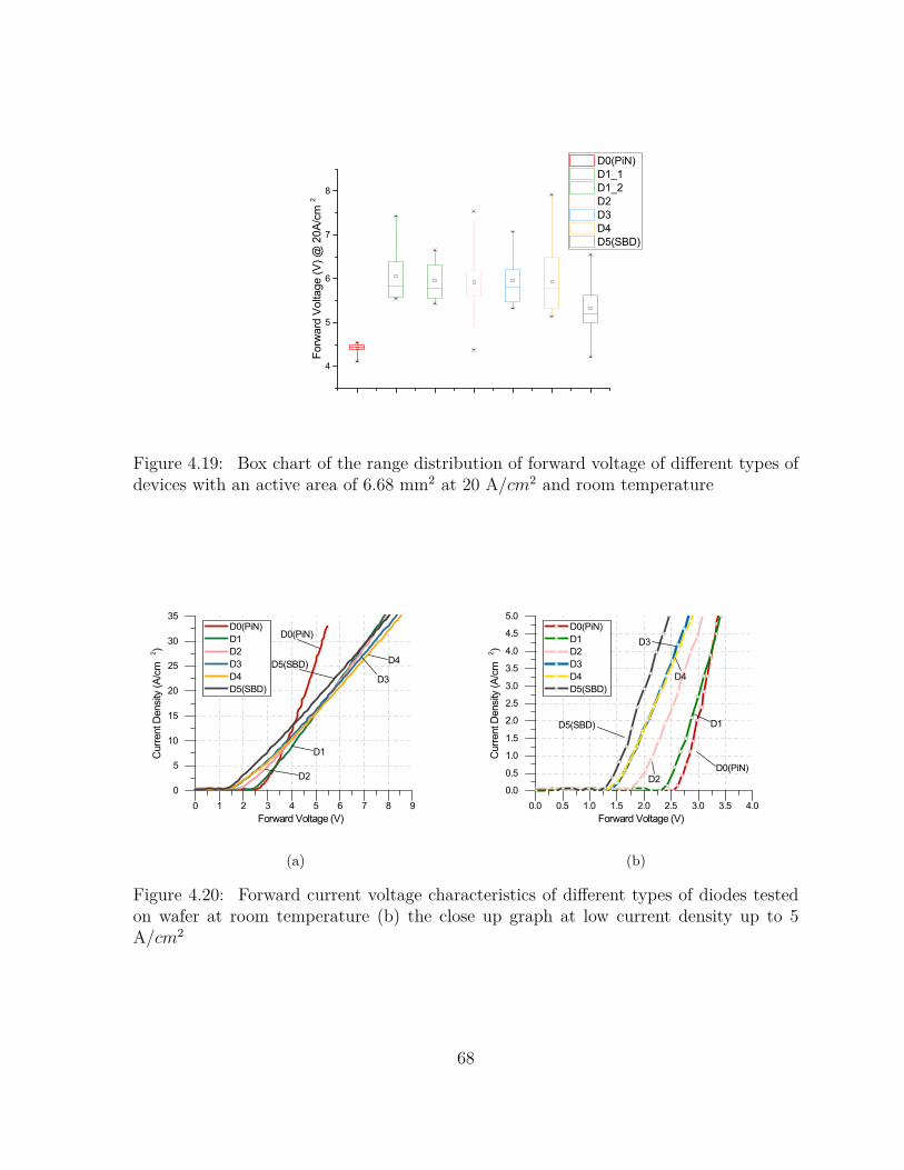
4
5
6
7
8
D0(PiN) D1_1 D1_2 D2 D3 D4 D5(SBD)
Forw
ard
Volta
ge (V
) @ 2
0A/c
m2
Figure 4.19: Box chart of the range distribution of forward voltage of different types ofdevices with an active area of 6.68 mm2 at 20 A/cm2 and room temperature
0 1 2 3 4 5 6 7 8 90
5
10
15
20
25
30
35
Cur
rent
Den
sity
(A/c
m2 )
Forward Voltage (V)
D0(PiN) D1 D2 D3 D4 D5(SBD)
D0(PiN)
D1
D4
D3D5(SBD)
D2
(a)
0.0 0.5 1.0 1.5 2.0 2.5 3.0 3.5 4.00.0
0.5
1.0
1.5
2.0
2.5
3.0
3.5
4.0
4.5
5.0
Cur
rent
Den
sity
(A/c
m2 )
Forward Voltage (V)
D0(PiN) D1 D2 D3 D4 D5(SBD)
D0(PiN)
D1
D4
D3
D5(SBD)
D2
(b)
Figure 4.20: Forward current voltage characteristics of different types of diodes testedon wafer at room temperature (b) the close up graph at low current density up to 5A/cm2
68

0 1 2 3 4 5 6 7 80
5
10
15
20
25
30
35
(b)
Cur
rent
Den
sity
(A/c
m2 )
Forward Voltage (V)
D0(PiN) D1 D2 D3 D4 D5(SBD)
D0(PiN)
D1
D5(SBD)
D3
D4
D2
(a)
0.0 0.5 1.0 1.5 2.0 2.5 3.0 3.5 4.00.00.51.01.52.02.53.03.54.04.55.0
Cur
rent
Den
sity
(A/c
m2 )
Forward Voltage (V)
D0(PiN) D1 D2 D3 D4 D5(SBD)
D0(PiN)
D1
D5(SBD)
D3
D4
D2
(b)
Figure 4.21: Forward current voltage characteristics of different types of diodes testedon wafer at 423 K (b) the close up graph at low current density up to 5 A/cm2
275 300 325 350 375 400 425 4503.5
4.0
4.5
5.0
5.5
6.0
6.5
7.0
7.5
8.0
8.5
(a)
Volta
ge (V
)
Temperature (K)
D0(PiN) D1 D2 D3 D4 D5(SBD)
(a)
300 325 350 375 400 425 4500
50
100
150
200
250
(b)
Diffe
rent
ial O
n-R
eiss
tanc
e (m
Ohm
-cm
2 )
Temperature (K)
D0(PIN) D1 D2 D3 D4 D5(SBD)
(b)
Figure 4.22: (a) Forward voltage of different types of diodes at 20 A/cm2 (b) Differentialon-resistance at 20 A/cm2 for different types of diodes at different temperature tested onwafer
69

the Schottky contact, more minority injection happens, which leads to the decreasing of
resistance with temperature. It is worth to notice that even without p-type region at the
active region, the forward voltage of D5 decreases at 423K. It may due to the overlap
between the first p-type ring of the edge termination and the anode contact, which will
also induce hole injection at certain states.
The MPS diodes were also packaged to further evaluate the performance. A DBC
based package was designed in FREEDM to withstand high temperature and high volt-
age [71] shown in Figure 4.23. The forward characteristics up to 498 K was shown in
Figure 4.24.
Figure 4.23: Packaged silicon carbide MPS diodes for high temperature operation withthermistor
4.3.3 Reverse Characteristics
The breakdown voltage is tested on top half of the wafer before putting polyimide and
dicing. The wafer has to be immersed in flourinert to avoid arcing at high voltage. The
map is shown in Figure 4.25 and Figure 4.26. The breakdown voltage is sensitive to
70

0 1 2 3 4 5 6 7 80.0
0.2
0.4
0.6
0.8
1.0
1.2
1.4
1.6
1.8
2.0
Cur
rent
(A)
Forward Voltage (V)
295 K 327 K 349 K 373 K 397 K 431 K 447 K 471 K 498 K
Figure 4.24: Forward I-V characteristics of a packaged MPS diode (D1) at elevatingtemperature up to 498 K
the defect on wafer generated during processing, especially on the edge termination.
No significant trend is revealed on the map of the breakdown voltages, and all types of
devices have dies with breakdown voltages larger than 10 kV. The reverse current-voltage
characteristics of these best devices with area of 6.68 mm2 are plotted in Figure 4.27.
No significant difference on leakage current is found for different structures, and even the
SBD (D5) has a very low leakage current, due to the high SBH and improved quality
of the interface between passivation and SiC. The distribution of breakdown voltage
of small devices The best reverse I-V of small devices (area of 1.13 mm2) is shown in
Figure 4.28. It has higher average breakdown voltage and also more devices with BV
higher than 9000 V compared to large devices. It shows that the defect generated during
process usually degrades the device performance, and small device is less affected by the
defects coming from various process steps. No significant difference of yield with different
edge termination structures are discovered. The best reverse I-V of these small devices
71

on wafer is demonstrated in Figure 4.29. They reveal higher breakdown voltage probably
due to less process and material defects, and the highest breakdown voltage achieved is
14.0 kV. This value is 96 % of simulated edge termination breakdown voltage and 88%
of the ideal drift region breakdown voltage. The edge termination design of the small
devices is introduced in section 3.1.3, type A design means Si = 0.0175, type B design
means Si = 0.0225, type C design means Si = 0.0275.
(a) (b)
Figure 4.25: Distribution of breakdown voltage (V) of (a) PiN diodes and (b) Schottkydiodes top half of the tested wafer
(a) (b)
Figure 4.26: Distribution of breakdown voltage (V) of (a) MPS diodes and (b) JBSdiodes on top half of the tested wafer
The comparison between the devices described in Chapter 3 [2] about best reverse I-V
characteristics of diodes is demonstrated in Figure 4.31. The material spec, the Aluminum
72

0 2000 4000 6000 8000 10000 12000 140001 x10-10
1 x10⁻⁹
1 x10⁻⁸
1 x10⁻⁷
1 x10⁻⁶
1 x10⁻⁵
1 x10⁻⁴
1 x10⁻³
D3
D5(SBD)
D2
D4
Leak
age
Cur
rent
(A)
Reverse Voltage (V)
D0(PiN) D1 D2 D3 D4 D5(SBD)
D0(PiN)
D1
Figure 4.27: Reverse I-V characteristics of for different types of devices with an activearea of 6.68 mm2 at room temperature
ion implant conditions along with the edge termination design in previous work is same
as this work. The difference is the frontside Schottky contact and the passivation stack
on edge termination area. The Schottky barrier height of the devices in previous study is
0.89 eV with ideality factor of 2.4, which does not have annealing process. Current work
shows better quality of the Schottky contact. The passivation layer of the previous work
only had one PECVD oxide layer and did not go through nitrous oxide annealing as well.
Moreover, the forward characteristics of this work is also better than the previous one,
as shown in Figure 4.32. It is worth to mention that for the previous work, the thermal
oxidation of the wafer before processing was done to enhance the lifetime to around 2
µm, which is higher than this wafer, which does not go through the lifetime enhancement
process. Except for the high Schottky barrier height which gives the benefit, it also proves
that the drift region lifetime is not critical anymore for this MPS diode as long as the
p-type region is formed by ion implantation.
73

Figure 4.28: Distribution of breakdown voltage (V) of small MPS diodes with differentedge termination designs (a) Si = 0.0175 um (b) Si = 0.0225 um (c) Si = 0.0275 um ontop half of the tested wafer
74

0 2000 4000 6000 8000 10000 12000 140001 x10-10
1 x10⁻⁹
1 x10⁻⁸
1 x10⁻⁷
1 x10⁻⁶
1 x10⁻⁵
1 x10⁻⁴
Leaa
kge
Cur
rent
(A)
Reverse Voltage (V)
A B C A
B
C
Figure 4.29: Reverse I-V characteristics of MPS(D1) with small active area (1.13 mm2)with different edge termination design
Figure 4.30: The leakage current under 5 kV for small MPS diodes before and afterpolyimide passivation
75

Figure 4.31: Reverse I-V characteristics of for different types of devices compared toprevious work [2]
Figure 4.32: forward voltage and leakage current of MPS diode compared to previouswork [2]
76

Despite the advantages, the devices show sort of degradation even after retest. Fig-
ure 4.33 shows the reverse I-V with first and second test with gap of over 12 hours. Both
PiN and SBD diodes show severe increasing leakage currents. One explanation could be
that some particle from the flourinert may gather in the edge termination area under
high electric field, and cause the redistribution of charges, thus degrade the performance.
In that case, a MPS diode is tested up to high temperature, and only with voltage up
to 2 kV, as shown in Figure 4.34. The device still has significant high leakage current at
200 C, and did not show degradation when back to room temperature under 2 kV.
(a) (b)
Figure 4.33: First and second time test of (a) SBD and (b) PiN diode reverse I-V withtime gap of over 12 hours
4.3.4 Reverse Recovery Characteristics
The reverse recovery performance of the diodes are tested with the circuit shown in
Figure 2.3, and the test setup is demonstrated in Figure 4.35. The SiC MOSFET is set
77

Figure 4.34: Reverse I-V characteristics of for MPS diodes at various temperature
as the switching device to control, and DC voltage is set as 1kV for safety. The device
is tested up to 473 K. When gate resistance is 20 Ω, the current waveform shows strong
oscillation with the parasitics. When gate resistance is increased to 100 Ω, the oscillation
was damped due to lower di/dt and dv/dt at that time. The comparison of parameters
with different gate driving speed is shown in Table 4.5. It shows the gate resistance has
a huge impact on the di/dt of the device, along with the peak reverse recovery current
during diode turn-off. The peak reverse recovery current is lowered significantly with
lower di/dt caused by larger gate resistance.
In both cases, when temperature is increasing, the reverse recovery charge is in-
creasing, which is predicted as the injection of the minorities increases. The relationship
between the reverse recovery charge and forward voltage of the MPS diode at various tem-
perature is shown in Figure 4.37, which clearly shows that when temperature increases,
the forward voltage decreases and the reverse recovery charge increases.
78
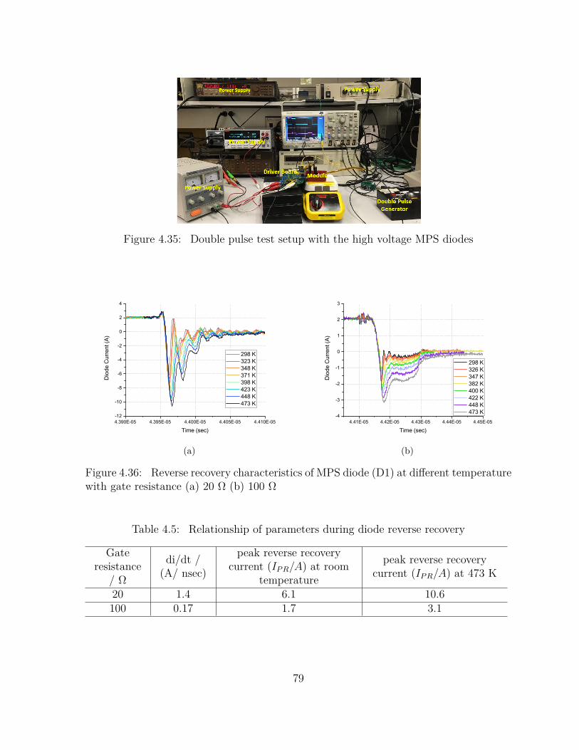
Figure 4.35: Double pulse test setup with the high voltage MPS diodes
4.390E-05 4.395E-05 4.400E-05 4.405E-05 4.410E-05-12
-10
-8
-6
-4
-2
0
2
4
Dio
de C
urre
nt (A
)
Time (sec)
298 K 323 K 348 K 371 K 398 K 423 K 448 K 473 K
(a)
4.41E-05 4.42E-05 4.43E-05 4.44E-05 4.45E-05-4
-3
-2
-1
0
1
2
3
Dio
de C
urre
nt (A
)
Time (sec)
298 K 326 K 347 K 382 K 400 K 422 K 448 K 473 K
(b)
Figure 4.36: Reverse recovery characteristics of MPS diode (D1) at different temperaturewith gate resistance (a) 20 Ω (b) 100 Ω
Table 4.5: Relationship of parameters during diode reverse recovery
Gateresistance
/ Ω
di/dt /(A/ nsec)
peak reverse recoverycurrent (IPR/A) at room
temperature
peak reverse recoverycurrent (IPR/A) at 473 K
20 1.4 6.1 10.6100 0.17 1.7 3.1
79

4.5 5.0 5.5 6.0 6.5 7.0 7.5 8.00
50
100
150
200
250
300
350
Rev
erse
Rec
over
y C
harg
e at
2 A
(nC
)
Forward Voltage (V) at 2 A (30 A/cm 2)
Increasing Temperature
Figure 4.37: The reverse recovery charge (Qrr versus forward voltage Vf of MPS diode(D1) with increasing temperature)
4.3.5 Reliability
One well-known issue with the reliability of silicon carbide high voltage bipolar power
devices is the bipolar degradation. It happens when device is under continuous forward
state, with minority carrier injected. The basal plane dislocation (BPD) will then act as
nucleation sites of Shockley Stacking faults (SSF), and the SSFs will expand and cause a
significant reduction in the carrier lifetime, leading to an increase in the forward voltage
drop in devices. The reverse leakage current will also potentially increase. Many studies
have discussed this phenomenon in high voltage epitaxial PiN diode, but much less on
the high voltage MPS diodes. One previous study [72, 73] shows the degradation of the
10 kV SiC MPS diodes, but the spaces under Schottky contact is wide (6 µm) and no
significant carrier injection is shown based on the IV curve at room temperature. At high
temperature up to 473 K the devices shows strong injection starting around 7 V. Even
at this case a severe degradation is observed, and it is closely related to the BPD density
80
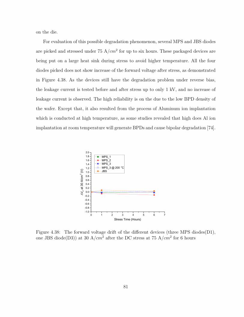
on the die.
For evaluation of this possible degradation phenomenon, several MPS and JBS diodes
are picked and stressed under 75 A/cm2 for up to six hours. These packaged devices are
being put on a large heat sink during stress to avoid higher temperature. All the four
diodes picked does not show increase of the forward voltage after stress, as demonstrated
in Figure 4.38. As the devices still have the degradation problem under reverse bias,
the leakage current is tested before and after stress up to only 1 kV, and no increase of
leakage current is observed. The high reliability is on the due to the low BPD density of
the wafer. Except that, it also resulted from the process of Aluminum ion implantation
which is conducted at high temperature, as some studies revealed that high does Al ion
implantation at room temperature will generate BPDs and cause bipolar degradation [74].
0 1 2 3 4 5 6 7-1.0-0.8-0.6-0.4-0.20.00.20.40.60.81.01.21.41.61.82.0
V F at 3
0 A/
cm2 (V
)
Stress Time (Hours)
MPS_1 MPS_2 MPS_3 MPS_3 @ 200 oC JBS
Figure 4.38: The forward voltage drift of the different devices (three MPS diodes(D1),one JBS diode(D3)) at 30 A/cm2 after the DC stress at 75 A/cm2 for 6 hours
81

4.3.6 Device Modeling
Physics based device modeling was also carried out to better understand the device be-
havior. Sentaurus TCAD was utilized as the tool with physics models listed in appendix.
For the forward characteristics, the unipolar JBS diode was chosen first, as it is easier
to model the unipolar device with less variables. The Schottky barrier height determines
the knee voltage, and the space between p-type regions(as the existing lateral straggling
model still not accurate), the backside Ohmic resistance was varied to match the differ-
ential on-state resistance. The mobility model, drift region doping concentration and the
substrate resistance can be achieved based on traditional models and data provided by
the supplier. Then the PiN diode was chosen to model. If using the value of the average
lifetime characterized by the µPCD technique shown in Figure 4.13, the simulated for-
ward performance of the PiN has lower resistance compared to the measured value. One
important reason is the low injection efficiency of the diode, and the lifetime inside the
p-type area should be low. This became the key parameter to adjust to fit the forward
characteristics of the diode. Then the MPS diode was modeled, where the knee voltage
is both determined by the space between p-type regions and the Schottky barrier height,
and the differential on-state resistance is also based on the space along with localized low
lifetime. It has been found though the localized lifetime is low, a small variation of that
value will cause a significant change in the forward characteristics, which became the
most crucial factor in determine the forward characteristics of ion implanted SiC bipolar
diodes.
The leakage current of the Schottky barrier diode(D5) was also modeled in Sentaurus
TCAD. Only Schottky barrier diode was chosen without p-type region to avoid possible
leakage path through the p-n junctions at high voltage, as discussed in Chapter 3. The
82

Figure 4.39: Comparison of the measured forward I-V characteristics to TCAD simula-tion results of PiN(D0), MPS(D1) and JBS(D4) at room temperature
Schottky barrier lowering and tunneling model was applied and adjusted to match the
measured device behavior. The simulation results shows similar trend of leakage current
increasing with voltage with measured results. The difference of the leakage current can
be from multiple sources, which is discussed in Table 2.3.
83

Figure 4.40: Comparison of the measured reverse I-V characteristics to TCAD simula-tion results of SBD(D5) at room temperature
84

Chapter 5
Design and Fabrication of 10-kV SiC
MPS Diodes with Improved
Structures
5.1 Device Design
5.1.1 Active Cell Design
Another round of fabrication of MPS diode was conducted aiming at improving the
performance. The active cell design is similar to the previous one, with the same ion
implantation schedule to form the p-type region in active area, and the same Schottky
contact process ensuring low leakage current and bipolar injection. One change is the
minimum feature size, which is limited as 2 µm due to using MA6 contact aligner as
the lithography tool, instead of the GCA stepper due to unstable performance. In the
new design, half-cell Schottky contact width Ws is set as 1.5 and 2 µm, and the half-cell
85
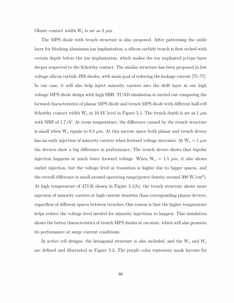
Ohmic contact width Wo is set as 2 µm.
The MPS diode with trench structure is also proposed. After patterning the oxide
layer for blocking aluminum ion implantation, a silicon carbide trench is first etched with
certain depth before the ion implantation, which makes the ion implanted p-type layer
deeper respected to the Schottky contact. The similar structure has been proposed in low
voltage silicon carbide JBS diodes, with main goal of reducing the leakage current [75–77].
In our case, it will also help inject minority carriers into the drift layer in our high
voltage MPS diode design with high SBH. TCAD simulation is carried out comparing the
forward characteristics of planar MPS diode and trench MPS diode with different half-cell
Schottky contact width Ws at 10 kV level in Figure 5.1. The trench depth is set as 1 µm
with SBH of 1.7 eV. At room temperature, the difference caused by the trench structure
is small when Ws equals to 0.5 µm. At this narrow space both planar and trench device
has an early injection of minority carriers when forward voltage increases. At Ws = 1 µm
the devices show a big difference in performance. The trench device shows that bipolar
injection happens at much lower forward voltage. When Ws = 1.5 µm, it also shows
earlier injection, but the voltage level at transition is higher due to bigger spaces, and
the overall difference is small around operating range(power density around 300 W/cm2).
At high temperature of 473 K shown in Figure 5.1(b), the trench structure shows more
injection of minority carriers at high current densities than corresponding planar devices,
regardless of different spaces between trenches. One reason is that the higher temperature
helps reduce the voltage level needed for minority injections to happen. This simulation
shows the better characteristics of trench MPS diodes at on-state, which will also promote
its performance at surge current conditions.
In active cell designs, the hexagonal structure is also included, and the Wo and Ws
are defined and illustrated in Figure 5.2. The purple color represents mask layouts for
86

(a) (b)
Figure 5.1: Comparison of forward characteristics of 10 kV conventional and trench MPSdiodes with different Schottky contact width Ws at (a) 300 K (b) 473 K
ion implantation forming p-type regions. It is defined in this way because the Ws has to
be the largest value that can be found in the Schottky regions, so that the electric field
location is least shielded from the p-type regions under reverse bias.
5.1.2 Edge Termination Design
As MA6 contact aligner can only have minimum feature of 2 µm, the multiple FFR
structure previous used is not suitable anymore, which requires narrow spaces down to
1 µm. In this case, the MFZ-JTE structure is adopted, which was discussed in section
3.1.3 having least impact from lateral straggling of ion implantation with the least space
needed. The original structure designed by Dr. Woongje Sung [3] is shown in Figure 5.3.
It has total width of 450 µm with 36 rings. The width of the ring plus the space on the
right of the ring is set as constant as 12.5 µm, and the ring width is decreasing with
numbers:
87

8.0E+12 1.0E+13 1.2E+13 1.4E+13 1.6E+134000
6000
8000
10000
12000
14000
16000
WsWsWsWsWs
Ws
Wo
Ws
Figure 5.2: basic cell parameters in hex structure design
Wn = W1/α(n−1) (5.1)
where W1 is 12.5 µm and n equals to 36. However, in our case the spaces between first
few rings are still too narrow to be defined by the lithography tool. To solve the problem,
the first 16 rings close to the active area is merged, and the spaces was opened starting
at 3 µm, as shown in Figure 5.3(b). Due to the merging, the parameters of dose and α
were redesigned. The breakdown voltages were simulated with different surface charge,
dose and α, as shown in Figure 5.5. Finally, dose=1.2e13 cm−2 was chosen and α was
varied between 1.01, 1.02 and 1.03 to evaluate the performance.
5.1.3 Layout Design
Previous simulation studies in chapter 2 show that increasing Ohmic contact width Wo
will improve MPS diodes’ performance at surge conditions. On the other hand, smaller
88

Figure 5.3: Orginal MFZ-JTE design for SiC high voltage devices [3]
Figure 5.4: Similar MFZ-JTE structure with first 16 rings merged
89

8.0E+12 1.0E+13 1.2E+13 1.4E+13 1.6E+134000
6000
8000
10000
12000
14000
16000
Brea
kdow
n Vo
ltage
(V)
Dose (cm -2)
=1.02 IC=0 =1.02 IC=5e11 =1.02 IC=1e12 =1.01 IC=0 =1.01 IC=5e11 =1.01 IC=1e12 =1.03 IC=0 =1.03 IC=5e11 =1.03 IC=1e12
Figure 5.5: Simulated breakdown voltage of MFZ-JTE with different interface charges(IC) (cm−2), doses, and α
half-cell width is always favored for distributing the current and keeping enough area of
with Schottky contact for conduction at unipolar state. The 5th generation of MPS diode
from Infineon has utilized a novel layout design with large size p-type area on certain
locations for conducting current at surge current conditions [78]. The reason is that under
surge conditions, the wide p-type area in the transition region between the active area
and edge termination will start to inject holes at first, which leads extremely high current
density only on the transition region, thus high heat is gathered and potential failure may
happen in the transition region. Adding the large p-type region in the active area helps
distribute this large high current and reduce the peak temperature. Similar approach is
adopted for the design of this high voltage MPS diodes. Big squares are added in the
stripe layouts, and the big hex structures are added in hexagonal layouts, as shown in
Figure 5.6. The colored area represents area open for p-type ion implantation, and the
90

white area is covered with Schottky contact. A closer look is shown in Figure 5.7, and
the parameters like the size of the big p-type region Wc and distance between the big
p-type region Wr are varied to validate the performance.
This kind of device with varying structure in different location of the die could not be
simulated or modeled with the conventional method, especially under extreme condition
like surge current. Traditionally the whole device is modeled as a repetitive combina-
tion of the basic cell which only has pitch of several microns. In device electro-thermal
simulations in the circuit, the device as a whole is considered a heat source. The die
was represented by one single SPICE model which usually represents the behavior of its
repetitive single cell, and the whole package around the die can be modeled by multi-
ple RC circuits. This method works under normal operating conditions, like continuous
switching between on and off state with certain frequency and duty ratios. In these cases,
the heat is distributed evenly across the whole area of the die and no heat or electro spikes
generated in a certain location of the die. But there are cases when device is going under
the extreme conditions, like unclamped inductive switching (UIS) or surge conditions.
Most often the current can not be distributed evenly across the die, and it sometimes
gathered in a specific location and cause failure. To model these kind of behavior, a
new method was proposed [79]. It divides power device into multiple macro-cells. The
size of macro-cell is much smaller than the full device area, but its much larger than
the device repetitive single cell. The number of macro-cells per device is limited only by
the computational power. Each maro-cell can be described by a separate SPICE model,
and depending on the design, it can be different at different locations. The macro-cells
connected each other with coupled electro and thermal models. It could be calibrated
by Finite Element Method (FEM) simulations. This method can be applied to the MPS
diode, especially with different structure at different locations, then the temperature dis-
91

tribution under surge condition can be depicted and optimized. Unfortunately it has not
been discussed in SiC MPS yet, which will be an interesting topic for future investigation.
(a) (b)
Figure 5.6: layout design for stripe and hex structures with large p-type areas
5.2 Fabrication Procedure
5.2.1 Starting Material
One 4-inch 4H-SiC wafer from Cree Inc was purchased for this fabrication. It has substrate
thickness 362.26 µm and resistivity of 0.018 Ωcm, and the micropipe density is 0.08 cm−2.
It has a first epitaxial layer of thickness 8 µm and doping concentration of 1e18 cm−3
and a second epitaxial layer of doping concentration 3.09e14 cm−3, and thickness of 99.04
µm. It has Si face surface with chemical-mechanical polishing ready. The minority lifetime
92

8.0E+12 1.0E+13 1.2E+13 1.4E+13 1.6E+134000
6000
8000
10000
12000
14000
16000
Wc Wr
(a)
8.0E+12 1.0E+13 1.2E+13 1.4E+13 1.6E+134000
6000
8000
10000
12000
14000
16000
Wc Wr
(b)
Figure 5.7: closer look on the layout design with parameters labeled
was characterized by micro photo conductive decay (µPCD) method all over the wafer
by Cree Inc, as shown in Figure 5.8.
5.2.2 Design of Process Flow
The summary of the process given in Table 5.2. Similar to the first run, most of the
process is carried out in NCSU nanofabircation facility (NNF) and shared material in-
strumentation facility (SMiF) in Duke University. But unlike last time, MA6 contact
aligner was utilized as the lithography tool. The advantage of using the tool is that it
is easy and convenient to operate, which saves plenty of time. It also enables the mask
to cover all of the wafer, instead of being restricted in a small size if using the stepper.
In that case, more design variations can be applied. However, it can not define features
less than 2 µm, which makes design adjusted as stated in section 4.1. It has one more
step of aluminum ion implantation, as p-tyep region formation was separated between
active area and edge termination. The first n-type and second lightly doped p-type ion
93
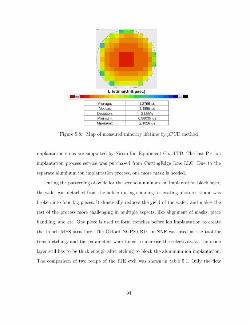
Figure 5.8: Map of measured minority lifetime by µPCD method
implantation steps are supported by Nissin Ion Equipment Co., LTD. The last P+ ion
implantation process service was purchased from CuttingEdge Ions LLC. Due to the
separate aluminum ion implantation process, one more mask is needed.
During the patterning of oxide for the second aluminum ion implantation block layer,
the wafer was detached from the holder during spinning for coating photoresist and was
broken into four big pieces. It drastically reduces the yield of the wafer, and makes the
rest of the process more challenging in multiple aspects, like alignment of masks, piece
handling, and etc. One piece is used to form trenches before ion implantation to create
the trench MPS structure. The Oxford NGP80 RIE in NNF was used as the tool for
trench etching, and the parameters were tuned to increase the selectivity, as the oxide
layer still has to be thick enough after etching to block the aluminum ion implantation.
The comparison of two recipe of the RIE etch was shown in table 5.1. Only the flow
94

rate of oxygen was increased, and the etch rate of silicon dioxide decreased, but the
selectivity of the SiC/SiO2 increased. It is consistent with the reported discovery [80],
which probably due to that adding oxygen will reduce the desorption rate of silicon
dioxide more significantly, compared to its influence on higher silicon carbide etch rate.
old recipe new recipeRIE Power (W) 200 200
O2 (sccm) 7.5 12SF6 (sccm) 24.5 24.5
pressure (mTorr) 40 40etch rate of SiC (nm/min) 67 50
selectivity of SiC/SiO2 0.83 2
Table 5.1: comparison of recipe for etching silicon carbide by Oxford NGP80 at NNF
Due to the trenches being made, the surface will not be flat before activation anneal-
ing. This condition brings challenge to the process, as conventionally a carbon layer has
to be coated on to the surface and being removed after annealing. The unflat surface will
bring challenge of uniform coating of the carbon layer to whole wafer and proper remov-
ing of it. A new activation annealing technique has been proposed from Toyo Tanso and
called Si vapor ambient anneal. Basically the Si source is attached to the inner surface
of the chamber made by TaC/Ta during annealing and provides silicon vapor, which will
helps removal of silicon carbide by forming gas of Si2C but suppress the desorption of
silicon atoms. In that case no capping layer is needed. By controlling the parameters, the
silicon carbide etching rate can be as low as several nanometers per minute, so that the
etched depth is negligible and the annealing can be achieved [81].
One problem happened during the backend process, that large part of the backside
thick metal was easily peeled off after deposition. It became worse during the dicing
95

Table 5.2: Fabrication Procedure
stepnumber
masknumber description
1 1 zero pattern and etch2 2 pattern and lift-off of Au for N+ ion implantation
3Nitrogen ion implantation (dose of
1× 10¹⁵/1× 1015/1× 1015/1× 1014 cm-2, and energy of30/70/100/120 keV at room temperature
4 strip deposited metal using acid
5 plasma enhanced chemical vapor deposition (PECVD) oxideof 1.5 µm for blocking SiC trench etch and ion implantation
6 3 pattern and etch deposited oxide for P+ ion implantation
7aluminum ion implantation (dose of
1.68× 10¹²/3.34× 1012/6.67× 1012/3.34× 1011 cm-2, andenergy of 30/70/140/300 keV at 500 C)
8 strip deposited oxide using buffered oxide etchant (BOE)9 4 pattern and etch deposited oxide for P+ ion implantation
10one piece of wafer experience reactive ion etching of siliconcarbide down to 0.5 µm before ion implantation with oxide
mask
11aluminum ion implantation (dose of
5× 10¹⁴/1× 1015/2× 1015/1× 1014 cm-2, and energy of30/70/140/300 keV at 600 C)
12 strip deposited oxide using buffered oxide etchant (BOE)
13 cap-free activation anneal with silicon vapor ambient at 1800C and 3 minutes by Toyo Tanso [81]
14 5front side passivation split (1) ALD oxide of 30nm and RTA
with N2O as ambient gas at 1000 C and 1 minute (2)without any oxide
15 HF dip before metal evaporation process
16 evaporation of nickel on the backside and RTA of 950 Cand 1 minute to form the Ohmic contact
17 HF dip before metal evaporation process
18 6 pattern and lift-off of nickel on frontside and RTA of 850 Cand 1 minute to form contacts
19 pattern and lift-off of Ti/Al for frontside metallization forfuture wire bonding process
20 7 polyimide (HD8820) coating, patterning and curing forpassivation and protection
21 deposition Ti/Ni/Au backside metallization for future dieattachment
22 dice and package
96

process, as the sticky blue tape has to be attached to the wafer backside during dicing,
and it leads to more metal being peeled off. Some samples maybe detached from the blue
tape during the dicing and being damaged. The potential improvement can be made on
(1) the backside protection added between the contact metal process and the thick metal
process, which is step 16-18 in Table 5.2. (2) the choice and parameters of backside metal
stacks have to be further optimized.
5.3 Characterization Results
5.3.1 Forward Characteristics
Due to the problem with backside metal, many devices showed unusual behaviors, like
much larger differential on-state resistance or significant voltage drift at high current
densities. Still some dies were able to be picked out with reasonable forward I-V behavior.
Figure 5.9 shows the forward characteristics of several MPS diodes with WS of 1.5 and 2
µm, and one PiN diode. The forward characteristics of the MPS diodes were similar to
each other, which is expected and agrees with the results in Chapter 4. The properties
of the Schottky barrier was extracted from the slope of the logI-V curve as shown in
Figure 5.10, and the SBH is 1.74 eV with ideality factor of 1.03. The differential on-state
resistance extracted is around 0.25 Ωcm2, which is close to the ideal on-resistance. The
knee voltage of MPS and PiN diodes are both the same as the result in the previous
run, and the differential on-resistance of the PiN diode is a bit larger than the result
in Chapter 4, which is probably due to the different parameters of activation anneal,
leading to different injection efficiencies. However, all the devices shows sort of shifting of
the characteristics when going to high current densities. This probably results from the
97

backside metal problem, which makes current gathering on local areas, and cause voltage
increasing. The contact resistivity of the frontside Ohmic contact extracted from TLM
structure was 2.6e-4 Ωcm2 as shown in Figure 5.11, which is higher than the results in
Chapter 4 but still acceptable, especially compared to the large resistance of the drift
layer.
Figure 5.9: Forward current voltage characteristics of different types of diodes tested onwafer with active area of 6.68 mm2
5.3.2 Reverse Characteristics
The map of breakdown voltage measured on wafer with ALD oxide as passivation is
shown in Figure 5.12. Different background color represents different parameters on edge
terminations, with red represents α = 1.01, green represents α = 1.02, and blue represents
α = 1.03. During the processing of the sample, some defects were introduced in the edge
98

Figure 5.10: Forward current voltage characteristics of the diode test structure withwhole active area covered with Schottky contact
(a) (b)
Figure 5.11: (a) the I-V curve of between the contacts of the TLM structures withdifferent space; (b) The extracted resistance versus spaces and the linear fit results
99

termination area, and causing some of the devices with zero breakdown voltage, indicating
that these parameters are not the main contribution to the difference of breakdown
voltage or leakage current. It may come from the edge termination area and determined
by the process of passivation layers. There are still several devices with breakdown voltage
over 10 kV available, and the highest one was 12454 V. The reverse I-V characteristics
of these devices are shown in Figure 5.13. The color of the lines represent different edge
termination designs. No significant trend is shown between different edge termination
designs or basic cell designs. Compared with the results in chapter 4, they have similar
breakdown voltage with the same active area. In the same time, the total width of the
edge termination (from edge of active area to edge of die) is 750 µm, which is 200 µm
smaller than the previous design. It causes the total die area to be 16 % smaller with
same active area of 6.68 mm2.
Figure 5.12: Distribution of breakdown voltage (V) of diodes tested on sample withALD oxide and polyimide as passivation layers
Another part of the wafer with trench MPS design was also evaluated for the break-
down voltage. The map of it is shown in Figure 5.14, and the reverse I-V characteristics
are shown in Figure 5.15. This sample has only polyimide as passivation, and it shows
100

0 1k 2k 3k 4k 5k 6k 7k 8k 9k 10k 11k 12k 13k1E-10
1E-9
1E-8
1E-7
1E-6
1E-5
1E-4
0.001
Leak
age
Cur
rent
(A)
Reverse Voltage (V)
stripe with Ws = 1.5 m, =1.01 stripe with Ws = 2 m, =1.01 stripe with Ws = 1.5 m, =1.03
Figure 5.13: Reverse I-V characteristics of for MPS diodes with different edge termina-tion design and Ws (active area 6.68 mm2)
generally higher leakage current compared to the previous sample. The higher leakage
current may either come from the p-type areas with trenches, or from the edge termina-
tion areas without oxide as passivation layers.
5.3.3 Surge Current Test Design
As stated in Chapter 2, usually a sinusoidal current has to be applied for the diode,
and different types of setup is reviewed. One simple way is to utilize a dc voltage source
in parallel with a capacitor and in series with an inductor, auxiliary switching and the
device under test(DUT). The LC oscillation will generate the sinusoidal waveform. The
duration and magnitude are determined by the value of the inductance, capacitance and
the DC voltage [82]. The other group revealed the setup for repetitive surge current
testing, where it let a high power IGBT working in amplifier mode, so that the output
101

Figure 5.14: Distribution of breakdown voltage (V) of diodes tested on sample withtrench structure and only polyimide as passivation
0 1k 2k 3k 4k 5k 6k 7k 8k 9k 10k 11k1E-10
1E-9
1E-8
1E-7
1E-6
1E-5
1E-4
0.001
Leak
age
Cur
rent
(A)
Reverse Voltage (V)
PiN diode stripe structure with Ws =1.5 m hex structure with Ws =1.5 m
Figure 5.15: Reverse I-V characteristics of for trench devices with active area of 6.68mm2 and α of 1.02
102

current of it can be controlled by the gate voltage, and repetitive sinusoidal current can
be generated [83].
Due to the issue that backside metal is not completely covered, currents will be
nonuniform across the die under surge current conditions, which results in voltage shift-
ing. As a result, the function of the various layout design on redistributing the current
will not be effective anymore, which will be dominant by the backside metal problem.
As all the available dies have shifting characteristics as shown in Figure 5.9 at high cur-
rent level, the surge test unfortunately won’t differentiate the performance with different
layout design, and poor surge behavior was observed on these dies.
103

Chapter 6
Conclusion and Future Work
In this thesis, the design, fabrication and characterization result of the high voltage (>
10 kV) silicon carbide MPS diodes have been demonstrated. The lateral straggling effect
was considered an important factor in designing high voltage devices. It is analyzed in
detail when designing the edge termination structures. For the first time, the process of
forming the Schottky contact on n-type drift region and Ohmic contact on p-type region
at the same time by Nickel was applied to fabricate a high voltage (>10 kV) SiC MPS
diode successfully. High Schottky barrier height (SBH) of 1.7 eV is achieved on n- drift
region with ideality factor close to one. The diodes achieved high breakdown voltage (14
kV) and extremely low leakage current, which has improved greatly compared to the
previous results from FREEDM center. The forward characteristics of different types of
devices and their dependence on temperature is compared and analyzed in detail.
The high voltage silicon carbide trench MPS diode structure and different designs
of the active area layout were proposed, aiming to improve the surge current capability.
Due to the trench structures, the cap-free Si vapor annealing technique was applied
in the fabrication process. The device demonstrates basic behavior within expectation,
104

especially having high breakdown voltage, which proves the functionality of the novel
annealing technique.
The future work in this direction of research includes:
1. Improve and optimize the fabrication process, which consists of (1) The backside
metal stack with so that devices can be made to fully evaluate the performance
based on the proposed trench MPS structure and various layout design;
2. More accurate models in describing the lateral straggling effect of ion implantation
with different parameters (substrate characteristics, implant angle, defect level in
different depth, effect of annealing)need to be developed;
3. More works are needed on understanding the defects in ion implanted p-type area
and its effect on the device performance (forward characteristics, leakage current,
surge capability, bipolar degradation and etc).Accurate physics based and behav-
ioral models need to be built under different ion implantation and annealing param-
eters. Moreover, alternative ways to improve the performance of this PN junction
with lower cost will be developed in prospect.
105

REFERENCES
[1] M. S. Jason, M. K. Linnarsson, Anders Hallen, and B. G. Svensson. Ion implantation
range distribution in silicon carbide. Journal of Applied Physics, 93, 2003.
[2] Edward Van Brunt. Development of optimal 4H-SiC bipolar power diodes for high
voltage high-frequency applications. PhD thesis, North Carolina State University,
2013.
[3] Woongje Sung, Edward Van Brunt, B. J. Baliga, and Alex Q. Huang. A new edge
termination technique for high-voltage devices in 4H-SiC —— multiple-floating-zone
junction termination extension. IEEE Electron Device Letters, 32:880–882, 2011.
[4] Alex Q. Huang, Mariesa L. Crow, Gerald Thomas Heydt, Jim P. Zheng, and
Steiner J. Dale. The Future Renewable Electric Energy Delivery and Manage-
ment(FREEDM) System: The Energy Internet. Proceedings of the IEEE, 99(1):133–
148, 2011.
[5] Alex Q. Huang and Jayant Baliga. FREEDM System: Role of power electronics and
power semiconductors in developing an energy internet. IEEE ISPSD, pages 9–12,
2009.
[6] W. McMurray. Multipurpose power converter circuits, Dec 1969.
[7] V. Pala, E. V. Brunt, M. O’Loughlin, J. Richmond, A. Burk, S. T. Allen, D. Grider,
J. W. Palmour, and C. J. Scozzie. 10 kV and 15 kV silicon carbide power MOSFETs
for next-generation energy conversion and transmission systems. Proc. IEEE ECCE,
pages 449–454, 2014.
106

[8] E. V. Brunt, L Cheng, MJ O’Loughlin, J Richmond, V Pala, and J. W. Palmour. 10
kV and 15 kV silicon carbide power MOSFETs for next-generation energy conversion
and transmission systems. pages 847–850, 2015.
[9] Qianlai Zhu, Li Wang, Liqi Zhang, Wensong Yu, and Alex Huang. Improved Medium
Voltage AC-DC rectifier based on 10 kV SiC MOSFET for solid state transformer
(SST) Application. Proc. IEEE APEC, pages 2365–2369, 2016.
[10] Li Wang, Qianlai Zhu, Dong Chen, Liqi Zhang, and Alex Huang. A Medium-Voltage
Medium-Frequency isolated DC-DC Transformer Based on Current Source Series
Resonant Converter and 15 kV SiC MOSFETs. IEEE Journal of Emerging and
Selected Topics in Power Electronics, 5(1), 2017.
[11] Qianlai Zhu, Li Wang, Alex Huang, Kristen Booth, and Liqi Zhang. 7.2 kV Single
Stage Solid State Transformer Based on Current Fed Series Resonant Converter and
15 kV SiC MOSFETs. IEEE Transactions on Power Electronics, page Early Access,
2018.
[12] T. Kimoto, A. Iijima, H. Tsuchida, T. Miyazawa, T. Tawara, A. Otsuki, T. Kato,
and Y. Yonezawa. Understanding and Reduction of Degradation Phenomena in SiC
Power Devices. Proc. IEEE IRPS, pages 2A–1.1 – 2A–1.7, 2017.
[13] Simon M.Sze and Kwok K. Ng. Physics of Semiconductor Devices. Wiley-
Interscience, 2006.
[14] B. Jayant Baliga. Silicon Carbide Power Devices: A 35 Year Journey from Concep-
tion to Commercialization. In 76th Device Research Conference, 2018.
107

[15] John W. Palmour. Silicon Carbide Power Device Development for Industrial Mar-
kets. In IEEE Internatioanl Electron Device Meeting, 2014.
[16] B. Jayant Baliga. Fundamentals of Power Semiconductor Devices. Springer, 2008.
[17] K. J. Schoen, J. P. Henning, J. M. Woodall, J. A. Cooper, and M. R. Melloch.
A Dual-Metal-Trench Schottky Pinch-Rectifier in 4H-SiC. IEEE Electron Device
Letters, 19(4), 1998.
[18] Chwan-Ying Lee, Cheng-Tyng Yen, Kuan-Wei Chu, and etc. A Novel 4H-SiC Trench
MOS Barrier Schottky Rectifier Fabricated by a Two-mask Process. Proc. IEEE
ISPSD, pages 171–174, 2013.
[19] Na Ren, Kang L.Wang, Zheng Zuo, Ruigang Li, and Kuang Sheng. A Novel 4H-SiC
Pinched Barrier Rectifier. Proc. IEEE APEC, 2017.
[20] P. A. Losse, C. Li, R. J. Kumar, T. P. Chow, I. B. Bhat, R. J. Gutmann, and R. E.
Stahlbush. Improving Switching Characteristics of 4H-SiC Junction Rectifiers using
Epitaxial and Implanted Anodes with Epitaxial Refill. ICSCRM, pages 1363–1366,
2005.
[21] B. J. Baliga. The pinch rectifier: A low-forward-drop high-speed power diode. IEEE
Electron Device Letters, 5(6), 1984.
[22] B. J. Baliga and Hsueh-Rong Chang. ”The merged P-I-N Schottky (MPS) rectifier:
A high-voltage, high-speed power diode”. In IEEE Internatioanl Electron Device
Meeting, 1987.
108
[23] Naoki Kaji, Hiroki Niwa, Jun Suda, and Tsunenobu Kimoto. Ultrahigh-Voltage SiC
p-i-n diodes with improved forward characteristics. IEEE Transactions on Electron
Devices, 62, 2015.
[24] Naoki Kaji, Hiroki Niwa, Jun Suda, and Tsunenobu Kimoto. Conductivity Mod-
ulated On-axis 4H-SiC 10+ kV PiN Diodes. Proc. IEEE ISPSD, pages 269–272,
2015.
[25] J. Suda H. Niwa and T. Kimoto. Ultrahigh-Voltage SiC MPS Diodes With Hybrid
Unipolar/Bipolar Operation. IEEE Transactions on Electron Devices, 64, 2017.
[26] M. Das, J. Sumakeris, B. Hull, J. Richard, S. Krishnaswami, and A. Powelli. Drift-
free, 50A, 10 kV 4H-SiC PiN Diodes with Improved Device yields. ECSCRM, pages
965–968, 2004.
[27] D. Okamoto and etc. 10-kV, 20-A 4H-SiC PiN diodes for power system applications.
Mater. Sci. Forum, 778-780:855–858, 2014.
[28] Brett Hull and etc. Development of Large Area(up to 1.5 cm2) 4H-SiC 10 kV
Junction Barrier Schottky Rectifiers. Mater. Sci. Forum, 600-603:931–934, 2009.
[29] Siddarth Sundaresan, Madhuri Marripelly, Svetlana Arshavsky, and Ranbir Singh.
15 kV SiC PiN diodes achieve 95% of avalanche limit and stable long-term operation.
Proc. IEEE ISPSD, pages 175–177, 2013.
[30] Hidenori Kitai, Yasuo Hozumi, Hiromu Shiomi, Masaki Furumai, Kazuhiro Omote,
and Kenji Fukuda. Demonstration of 13-kV Class Junction Barrier Schottky Diodes
in 4H-SiC with Three-Zone Junction Termination Extension. Mater. Sci. Forum,
897:451–454, 2017.
109

[31] B. Jayant Baliga. Silicon Carbide Power Devices. World Scientific, 2006.
[32] Tsunenobu Kimoto and James Cooper. Fundamentals of Silicon Carbide Technology:
Growth, Characterization, Devices and Applications. Wiley-IEEE Press, 2014.
[33] H. Lendenmann, A. Mukhitdinov, F. Dahlquist, H. Bleichner, M. Irwin, R. Soder-
holm, and P. Skytt. ”4.5kV 4H-SiC diodes with ideal forward characteristic”. In
International Symposium on Power Semiconductor Devices and ICs (ISPSD), 2001.
[34] Koutarou Kawahara, Giovanni Alferi, and Tsunenobu Kimoto. Detection and depth
analyses of deep levels generated by ion implantation in n- and p- type 4H-SiC.
Journal of Applied Physics, 106, 2009.
[35] Josef Lutz, Heinrich Schlangenotto, Uwe Scheuermann, and Rik De Doncker. Semi-
conductor Power Devices: Physics, Characteristics, Reliability. Springer, 2018.
[36] T T Mnatsakanov M E Levinshtein, A K Agarwal, and J W Palmour. Analytical
and numerical studies of p+ - emitters in silicon carbide bipolar devices. Semicond.
Sci. Technol., 26, 2011.
[37] J.J. Sumakeris and etc. Techniques for Minimizing the Basal Plane Dislocation
Density in SiC Epilayers to Reduce Vf Drift in SiC Bipolar Power Devices. ICSCRM,
pages 141–146, 2006.
[38] R. Nipoti, M. Puzzanghera, and G. Sozzi. Al ion implanted 4H-SiC vertical pin
diodes: Processing dependence of leakage currents and OCVD carrier lifetime. EC-
SCRM, pages 439–442, 2016.
110

[39] T. Kimoto, N. Miyamoto, A. Schoner, A. Saitoh, H. Matsunami, K. Asano, and
Y. Sugawara. High energy (MeV) Al and B ion implantation into 4H-SiC and
fabrication of pin diodes. Journal of Applied Physics, 91, 2002.
[40] B. Jayant Baliga. Advanced Power Rectifier Concepts. Springer US, 2009.
[41] Takashi Katusno, Yukihito Watanabe, Hirokazu Fujiwara, Masaki Konishi, Hideki
Naruoka, Jun Morimoto, Tomoo Morino, and Takeshi Endo. Analysis of surface
morphology at leakage current sources of 4H-SiC Schottky barrier diodes. Applied
Physics Letters, 98, 2011.
[42] M. Bhatnagar, B. J. Baliga, H. R. Kirk, and G. A. Rozgonyi. Effect of Surface
Inhomogeneities on the Electrical Characteristics of SiC Schottky Diodes. IEEE
Transactions on Electron Devices, 43, 1996.
[43] Dohyun Lee, Changyun Kim, Hunhee Lee, Suhyeong Lee, Hongjeon Kang, Hyun-
woo Kim, Huikyung Park, Jaeyeong Heo, and Hyeong Joon Kim. Improving the
Barrier Height Uniformity of 4H-SiC Schottky Barrier Diodes by Nitric Oxide Post-
Oxidation Annealing. IEEE Electron Device Letters, 35(8), 2014.
[44] K. Ohtsuka, T. Nakatani, A. Nagae, H. Watanabe, Y. Nakaki, Y. Fujii, K. Fujihira,
S. Nakata, and N. Yutani. Defect Related Leakage Current Components in SiC
Schottky Barrier Diode. Defects-Recognition, Imaging and Physics in Semiconduc-
tors XIV, pages 53–56, 2012.
[45] Ashish Kumar, Kasunaidu Vechalapu, Subhashish Battacharya, Victor Veliadis, Ed-
ward Van Brunt, and etc. Effect of capacitive current on reverse recovery of body
diode of 10kV SiC MOSFETs and external 10kV SiC JBS diodes. 5th Workshop on
Wide Bandgap Power Devices and Applications(WiPDA), pages 208–212, 2017.
111

[46] Yaren Huang and Gerhard Wachutka. Comparative Study of Contact Topographies
of 4.5kV SiC MPS Diodes for Optimizing the Forward Characteristics. Simulation
and Semiconductor Processes and Devices (SISPAD), pages 117–120, 2016.
[47] Hongyi Xu, Jiahui Sun, Jingjing Cui, Jiupeng Wu, Hengyu Wang, Shu Yang, Na Ren,
and Kuang Sheng. Surge Capability of 1.2kV SiC Diodes with High Temperature
Ion Implantation. Proc. IEEE ISPSD, pages 419–422, 2018.
[48] A. Zhang, S. Reshanov, A. Shoner, W. Kaplan, N. Kwietiewski, and J. K. Lim.
Planarization of epitaxial SiC trench structures by plasma ion etching. ECSCRM,
pages 549–552, 2014.
[49] F. J. Santos Rodriguez, D. Schloegl, F. Hille, P. C. Brandt, M. Pfaffenlehner, A. R.
Stegner, and A. Haertl. Novel Emitter Controlled Diode with copper metallization in
ultrathin wafer technology: setting a performance benchmark. Proc. IEEE ISPSD,
pages 121–122, 2017.
[50] Maolong Ke, Daohui Li, Xiaoping Dai, Huaping Jiang, Ian Deviny, Haihui Luo,
and Guoyou Liu. Improved Surge Current Capability of Power Diode with Copper
Metallization and Heavy Copper Wire Bonding. Power Electronics and Applications
(EPE’16 ECCE Europe), 2016.
[51] Josef Lutz, Roman Baburske, Min Chen, Birk Heinze, Matin Domeij, Hans-Peter
Felsl, and Hans Jonachim Schulze. The nn+ Junction as the key to improved rugged-
ness and soft recovery of power diodes. IEEE Transactions on Electron Devices, 56,
2009.
[52] Tomoko Matsudai, Tsuneo Ogura, Yuuichi Oshino, Taichi Kobayashi, Shinichiro
Misu, Yoshiko Ikeda, and Kazutoshi Nakamura. Advanced Cathode and Anode
112
Injection Control Concept for 1200 V SC (Schottky Controlled Injection) - Diode.
Proc. IEEE ISPSD, pages 19–22, 2014.
[53] Xin Tong, Zhuo Yang, Ye Tian, Fangjuan Bian, Siyang Liu, Weifeng Sun, Yuanzheng
Zhu, and Peng Ye. Influence of forward current freewheeling time on di/dt robustness
of SJ-MOSFET body diode. Proc. IEEE IPFA, pages 1–4, 2017.
[54] Kazuhiro Mochizuki, Norifumi Kameshiro, Hidekatsu Onose, and Natsuki
Yokoyama. Influence of lateral spreading of implanted aluminum ions and
implantation-induced defects on forward current-voltage characteristics of 4H-SiC
junction barrier Schottky diodes. IEEE Transactions on Electron Devices, 56, 2009.
[55] K. Mochizuki and H. Onose. Dual-Pearson Approach to Model Ion-Implanted Al
concentration profiles for high-precision design of high-voltage 4H-SiC power devices.
ICSCRM, pages 607–610, 2007.
[56] Kazuhiro Mochizuki and Natsuki Yokoyama. Two-dimensional analysis model for
concentration profiles of aluminum implanted into 4H-SiC (0001). IEEE Transac-
tions on Electron Devices, 58, 2011.
[57] Giorgio Lulli and Roberta Nipoti. 2D simulation of under-mask penetration in 4H-
SiC implanted with Al(+) ions. ECSCRM, pages 421–424, 2010.
[58] H. Bartolf, U. Gysin, H . R. Rossmann, A. Bubendorf, T. Glatzel, T. A. Jung,
E. Meyer, M. Zinnermann, S. Reshanov, and A. Schoner. ”Development of power
semiconductors by quantitative nanoscale dopant imaging”. In International Sym-
posium on Power Semiconductor Devices and ICs (ISPSD), 2015.
113

[59] H. R. Rossmann, U. Gysin, A. Bubendorf, T. Glatzel, S. A. Reshanov, A. Schoner,
T. A. Jung, E. Meyer, and H. Bartolf. Two-dimensional carrier profiling on lightly
doped n-type 4H-SiC epitaxially grown layers. ECSCRM, pages 269–272, 2014.
[60] R. Elpelt, B. Zippelius, S. Doering, and U. Winkler. Employing Scanning Spreading
Resistance Microscopy (SSRM) for improving TCAD simulation accuracy of silicon
carbide. ECSCRM, pages 295–298, 2016.
[61] M. buzzo, Mauro Ciappa, M .Stangoni, and W. Fichtner. Two-dimensional dopant
profiling and imaging of 4H silicon carbide devices by secondary electron potential
contrast. Microelectronics Reliability, pages 1499–1504, 2005.
[62] Yifan Jiang, Woongje Sung, Xiaoqing Song, Haotao Ke, Siyang Liu, Jayant Baliga,
Alex Q. Huang, and Edward Van Brunt. 10 kV SiC MPS diodes for high temperature
applications. Proc. IEEE ISPSD, pages 43–46, 2016.
[63] Woongje Sung and B. J. Baliga. A near ideal edge termination technique for 4500
V 4H-SiC devices: the hybrid junction termination extension. IEEE Electron Device
Letters, 37:1609–1612, 2016.
[64] Arash Salemi, Hossein Elahipanah, Keijo Jacobs, and Carl-Mikael Zetterling. 15 kV-
class implantation-free 4H-SiC BJTs with record high current gain. IEEE Electron
Device Letters, 39:63–66, 2018.
[65] Woongje Sung and B. J. Baliga. monolithically integrated 4H-SiC MOSFET and
JBS diode (JBSFET) using a single Ohmic/Schottky process scheme. IEEE Electron
Device Letters, 37:1605–1608, 2016.
114

[66] S. Tanimoto, H. Okushi, and K. Arai. Silicon Carbide - Recent Major Advances.
Springer, 2004.
[67] Xiangyu Yang, Bongmook Lee, and Veena Misra. Electrical Characteristics of SiO2
deposited by atomic layer deposition on 4H-SiC after nitrous oxide anneal. IEEE
Transactions on Electron Devices, 63, 2016.
[68] R. F. Schmitsdof, T. U. Kampen, and W. Monch. Explanation of the linear cor-
relation between barrier heights and ideality factors of real metal-semiconductor
contacts by laterally nonuniform Schottky barriers. Journal of Vacuum Science
Technology, 15, 1997.
[69] P. B. Klein, R. Myers-Ward, K-K Lew, B. L. VanMill, C. R. Eddy Jr, D. K. Gaskill,
A. Shrivastava, and T. S. Sudarshan. Recombination processes controlling the carrier
lifetime in n- 4H-SiC epilayers with low Z 12
concentration. Journal of Applied Physics,
108:033713, 2010.
[70] Takafumi Okuda, Tetsuya Miyazawa, Hidekazu Tsuchida, Tsunenobu Kimoto, and
Jun Suda. Enhancement of carrier lifetime in lightly Al-doped p-type 4H-SiC epi-
taxial layers by combination of thermal oxidation and hydrogen annealing. Applied
Physics Express, 7, 2014.
[71] Xin Zhao, Haotao Ke, Yifan Jiang, Adam Morgan, Yang Xu, and Douglas Hopkins.
A high performance power module with > 10 kV capability to characterize and test
in situ SiC devices at > 200 ambient. HiTEC, 2016.
[72] Qingchun Zhang, Anant Agarwal, Albert Burk, Michael O Loughlin, John Palmour,
Robert Stahlbush, and Charles Scozzie. Influence of Shockley Stacking Fault Gener-
115

ation on Electrical Behavior of 4H-SiC 10 kV MPS diodes. ICSCRM, pages 331–334,
2009.
[73] J.D. Caldwell, R. E. Stahlbush, E. A. Imhoff, K. D. Hobart, M. J. Tadjer, Q. Zhang,
and A. Agarwal. Recombination-induced stacking fault degradation of 4H-SiC
merged-PiN-Schottky diodes. Journal of Applied Physics, 106, 2009.
[74] Yuan Bu, Hiroyuki Yoshimoto, Naoki Watanabe, and Akio Shima. Fabrication of
4H-SiC PiN diodes without bipolar degradation by improved device process. Journal
of Applied Physics, 122, 2017.
[75] Masatoshi Aketa, Yuta Tokosuji, Mineo Miura, and Takashi Nakamura. 4H-SiC
trench structure Schottky diodes. ICSCRM, pages 933–936, 2011.
[76] Qingchun Zhang, Jennifer Duc, Van Mieczkowski, Brett Hull, Schott Allen, and J. W.
Palmour. 4H-SiC trench Schottky diodes for next generation products. ECSCRM,
pages 781–784, 2012.
[77] Kumiko Konishi, Norifumi Kameshiro, Natsuki Yokoyama, Akio Shima, and Ya-
suhiro Shimamoto. Influence of trench structure on reverse characteristics of 4H-SiC
Schottky diodes. ECSCRM, pages 596–599, 2014.
[78] Roland Rupp, Rolf Gerlach, and Andre Kabakow. Current distribution in the various
functional areas of a 600 V SiC MPS diode in forward operation. ICSCRM, pages
929–932, 2011.
[79] Giovanni Breglio, Andrea Irace, Luca Maresca, and Michele Riccio. Electro-thermal
simulations of Power Semiconductor Devices during high stress events. ESARS-
ITEC, 2018.
116

[80] K. Hiramatsu, T. Okuda, J. Suda, and T. Kimoto. High selectivity in SiC/SiO2
Etching by ICP-RIE in a SF6-O2-Ar chemistry. ECSCRM, 2016.
[81] Satoshi Torimi, Satoru Nogami, and Tadaaki Kaneko. Development of a novel cap-
free activation annealing technique of 4H-SiC by si-vapor ambient annealing using
TaC/Ta compposite materials. ICSCRM, pages 673–676, 2013.
[82] D Sadik, S Heinig, K Jacobs, D Johannesson, J Lim, M Nawaz, F Dijkhuizen,
M Bakowski, S Norrga, and H Nee. Investigation of the surge current capability
of the body diode of SiC MOSFETs for HVDC applications. ECCE Europe, 2016.
[83] S Palanisamy, J Kowlasky, J Lutz, T Basler, R. Rupp, and J M-Fallah. Repetitive
surge current test of SiC MPS diode with load in bipolar regime. Proc. IEEE ISPSD,
pages 367–370, 2018.
117

APPENDIX
118

Appendix A
Models for Numerical Simulation of
4H-SiC Power Devices
A.1 Simulation Models
119

Table A.1: Simulation Models and Parameters
Physical Properties Models
Bandgap Eg = 3.265− 0.011T 2
32744.3 + T
Bandgap Narrowing ∆Eg = 0.02(lnN
1× 10¹⁷+ (ln
N
1× 10¹⁷+ 0.5)0.5)
Intrinsic CarrierDensity
Nc = 1.695× 10¹⁹(T
300)3/2
Nv = 6.475× 10¹⁹(T
300)3/2
Mobilityµn =
1000( T300
)2.4 − 1.6
1 + ( N1.804×1017
)0.561
µp =125( T
300)2.15 − 1.074
1 + ( N1.279×1019
)0.333
High Field Mobility µhigh =µlow
(1 + ( µlowE
2.2×10⁷( T300
)−0.44 )1.2T300 )
3001.2T
Auger Recombination RAuger =3× 10⁻²⁹n+ 3× 10⁻²⁹p
np− (nieff )2
RecombinationLifetime
τ = (τmax
1 + N7×1016
)(T
300)1.5
Impact Ionization
αn = 2.10× 10⁷exp(−1.7× 10⁷
E)
αp = 2.96× 10⁷(1 + 7.511× 10⁻³(T − 300))
exp(−1.6× 10⁷(1 + 1.381× 10⁻³(T − 300))
E)
120

Incomplete IonizationNA
− =NA
1 + 4p/pI; pI = NV e
− 0.23−1.8×10⁻⁸Ni1/3
kBT
ND+ =
ND
1 + 2n/nI
;nI = NCe− 0.0525−3.38×10⁻⁸Ni
1/3
kBT
Schottky BarrierLowering
∆ΦB(F ) = 3×10⁻⁴((F
F0
)0.5−(Feq
F0
)0.5) if F > Feq
∆ΦB(F ) = 0 if F ≤ Feq
121