Embed Size (px)
Citation preview

Charge transport in InAs nanowire Josephson junctions
Simon Abay,1, ∗ Daniel Persson,1 Henrik Nilsson,2 Fan Wu,1 H.Q.
Xu,2, 3 Mikael Fogelstrom,1 Vitaly Shumeiko,1 and Per Delsing1, †
1Department of Microtechnology and Nanoscience (MC2),Chalmers University of Technology, SE-412 96 Goteborg, Sweden
2Division of Solid State Physics, Lund University, Box 118, S-221 00 Lund, Sweden3Key Laboratory for the Physics and Chemistry of Nanodevices andDepartment of Electronics, Peking University, Beijing 100871, China
(Dated: December 16, 2013)
We present an extensive experimental and theoretical study of the proximity effect in InAsnanowires connected to superconducting electrodes. We fabricated and investigated devices withsuspended gate controlled nanowires and non-suspended nanowires, with a broad range of lengthsand normal state resistances. We analyze the main features of the current-voltage characteristics:the Josephson current, excess current, and subgap current as functions of length, temperature, mag-netic field and gate voltage, and compare them with theory. The Josephson critical current for ashort length device, L = 30 nm, exhibits a record high magnitude of 800 nA at low temperaturethat comes close to the theoretically expected value. The critical current in all other devices is typ-ically reduced compared to the theoretical values. The excess current is consistent with the normalresistance data and agrees well with the theory. The subgap current shows large number of struc-tures, some of them are identified as subharmonic gap structures generated by Multiple AndreevReflection. The other structures, detected in both suspended and non-suspended devices, have theform of voltage steps at voltages that are independent of either superconducting gap or length ofthe wire. By varying the gate voltage in suspended devices we are able to observe a cross overfrom typical tunneling transport at large negative gate voltage, with suppressed subgap current andnegative excess current, to pronounced proximity junction behavior at large positive gate voltage,with enhanced Josephson current and subgap conductance as well as a large positive excess current.
I. INTRODUCTION
Semiconducting nanowires (NW) have been a focusof intensive research for their potential applications asbuilding blocks in nano-scale devices.1–4 The nano-scaledimension of the semiconducting nanowires, compara-ble to the electronic Fermi wave length, also makesthem an attractive platform for studying the fundamen-tal phenomena of quantum transport. By tuning theFermi wavelength by means of electrostatic gates onegets access to such quantum phenomena as conductancequantization,5,6 and quantum interference effects.7
Another research interest has been the proximity effectin nanowires induced by connecting them to supercon-ducting electrodes (S).8,9 In such devices, S-NW-S, thenanowire serves as a weak link through which a supercur-rent can flow due to the presence of the phase differencebetween the superconducting condensates.9–11
Among a variety of nanowires tested in experiments,nanowires of InAs play a central role.8,10 This isdue to their material properties: high electron mo-bility, low effective mass, and pinning of the Fermilevel in the conduction band that permits highlytransparent galvanic S-NW contacts. Hybrid de-vices of InAs nanowires have demonstrated Andreevsubgap conductance,6,12,13 Josephson field effect,9,10
and Cooper-pair beam splitting.14 More recently, thenanowire hybrid devices attracted new attention follow-ing theoretical predictions of Majorana bound states inNW-S proximity structures.15–17
In spite of intensive research, no systematic investiga-tion of the proximity effect in InAs nanowires has beenreported, leaving open important questions about consis-tency of the observed transport phenomena and theoret-ical views of the proximity effect.
In this paper, we report on extensive experimentalstudies of current-voltage characteristics (IVC) of a largevariety of hybrid devices made with InAs nanowires con-nected to aluminum electrodes. These Al-InAs NW-Aldevices include suspended and non-suspended nanowires,nanowires with different lengths, and tested at differ-ent temperatures, magnetic fields, and gate voltages.We measured the main proximity effect characteristics:Josephson critical current, excess current, and subgapcurrent features, and we make a quantitative comparisonwith relevant theoretical models.
Our main conclusion is that the most properties ofthe proximity effect can be qualitatively understood andquantitatively reasonably well fit on the basis of existingtheory. In particular, the record high Josephson criti-cal current of 800 nA, observed in the shortest studiednanowire (with 30 nm separation between superconduct-ing electrodes) is close to the theoretical bound for bal-listic point contacts.18 In longer devices, the decay of thecritical current with length is consistent with a cross overfrom ballistic to diffusive transport regime, followed bycross over from a short- to long-junction behavior.
In the gate controlled suspended devices we observea cross over from a distinct S-normal metal-S (SNS)type behavior with large positive excess current and en-
arX
iv:1
311.
1745
v2 [
cond
-mat
.sup
r-co
n] 8
Nov
201
3

2
hanced subgap conductance to tunneling S-inslulator-S(SIS) type behaviour in accordance with gradual deple-tion of the conducting channels by the gate potential andincrease of the wire resistance.
We also observe subgap current features associatedwith Multiple Andreev Reflection (MAR) transport. Inaddition to those MAR features we systematically ob-serve subgap features, which are not associated withMAR but have some different origin. These features arenot related to phonon-induced resonances,19 and they donot seem to have an electromagnetic origin. They ap-pear on the IVCs as voltage steps, strikingly similar tothe voltage steps generated by phase slip centers in su-perconducting whiskers.20,21
The structure of the paper is as follows: After de-scribing the device fabrication and experimental setupin Section II, we summarize the normal state conductionproperties of the devices in Section III, which give thenecessary input for choosing an appropriate theoreticalmodel of the proximity effect described in Section IV.Then in the following sections we discuss the supercon-ducting transport properties: excess current in SectionV, critical current in Section VI, sub gap current, andvariation of the current under the gate potential in Sec-tion VII. Section IX contains conclusive remarks.
II. EXPERIMENTAL DETAILS
A. Sample Fabrication
The devices we have investigated are of three types:nanowires placed directly on the substrate with eithera) two superconducting contacts or b) multiple contacts,and c) suspended devices with local gates (Fig. 1). Alldevices are made on standard Si substrates capped by400 nm thick SiO2.
The nanowires are grown by chemical beam epitaxy.22
In the growth process, metal-organic gaseous sources arethermally cracked to their components and the growthmaterials are directed as a beam towards an InAs sub-strate placed in the growth chamber. At the optimaltemperature, the nanowire growth is catalyzed by Auaerosol particles that have been distributed on the sub-strate. The sizes of the Au-seeds determine the diameterof the nanowires. In this paper, the nanowires are takenfrom a single growth batch with an average diameter of80 nm.
To fabricate the non-suspended devices, InAsnanowires are first transferred to a Si substrate and theirrelative positions with respect to predefined marks aredetermined with the help of scanning electron microscope(SEM) images. The extracted locations are then usedto pattern superconducting Ti/Al (5/150 nm thick) con-tacts on top of the nanowires. Depending on the intendeddevice length, i.e. distance between source and drainelectrodes, the superconducting contacts are defined byeither single-step or double-step electron beam (e-beam)
FIG. 1. SEM images of investigated devices. (a) Short lengthdevice of type A defined by a single-step electron-beam lithog-raphy (inset shows a short length device defined by a double-step e-beam lithography). (b) Device of type B has multiplecontacts on a single nanowire separated by different lengths.(c) Three-terminal device with a suspended nanowire and anearby local gate, the gate is 15 nm below the nanowire.
lithography.11 The shorter devices (L < 100 nm) are de-fined by the double-step e-beam lithography whereas thelonger devices (L ≥ 100 nm) are defined by the single-step e-beam lithography. A SEM image of a typical twoterminal device (L ≈ 100 nm defined by the single e-beamlithography) is shown in Fig. 1a. The inset image shows

3
a short length device of L ≈ 60 nm defined by the double-step e-beam lithography.
To fabricate the suspended devices, a standard Sisubstrate is first patterned with interdigitated Ti/Austripes.23 InAs nanowires are then transferred to the al-ready patterned Si substrate and some of the nanowiresend up on top of the interdigitated metal stripes. Thestripes are patterned in a two-step fabrication process inorder to get a height difference of 15 nm between everytwo adjacent stripes. This allows the nanowires to reston the thicker electrodes (65 nm thick) while being sus-pended above the substrate and the thinner electrodes(50 nm thick). With the help of SEM images, the posi-tions of suitable nanowires are found and superconduct-ing electrodes Ti/Al (5/150 nm thick) are defined on se-lected nanowires with e-beam lithography. A SEM imageof a suspended device is shown in Fig. 1c.
To get good transparency of the metal-nanowire inter-faces, an ammonium polysulfide solution (NH4Sx) clean-ing process11,24 has been used prior to evaporation of thesuperconducting contacts. The samples are then charac-terized at room temperature and stored in a vacuum boxbefore further measurements at low temperatures.
B. Experimental setup
Current-voltage characteristics of the devices are mea-sured in a dilution refrigerator with a base temperatureof 15 mK. The IVCs are recorded in either current orvoltage bias configuration. In the current-bias mode, thecurrent is determined by a high resistance bias resistorin series with the device. As we increase the current,the voltage across the device is simultaneously measuredwith a differential amplifier. In the voltage-bias mode,a voltage is directly applied across the device while thecurrent is measured simultaneously by a transimpedanceamplifier. To decrease noise coupling to the devices, theelectrical lines in the measurement set up are well fil-tered and thermally anchored at different temperaturestages of the refrigerator. The measurement setup is alsodesigned to measure IVCs as a function of temperatureand magnetic field.
C. Current-voltage characteristics
A typical IVC is shown in Fig. 2 for a device of lengthL ≈ 150 nm (sample B5a in Table I). Above the crit-ical temperature Tc ≈ 1.1 K, the IVC (blue) exhibitsOhmic behavior with a normal-state resistance of Rn =1.07 kΩ. At temperatures well below Tc, the IVC (red)shows three distinct conductance regimes. i) For volt-ages |V | > 2∆/e, the IVC shows a linear behaviour withthe same resistance as in the normal state, Rn. ii) Forsmaller voltages, |V | < 2∆/e, the resistance is approx-imately Rn/2 and exhibits subgap features. iii) At the
zero voltage V = 0, the device switches to zero-resistance,exhibiting a Josephson current.
In the next sections we perform quantitative analysisof the IVC, based on a detailed characterization of thenormal state current transport in the wire.
III. NORMAL STATE TRANSPORT
In order to characterize the normal-state properties ofthe junctions, dc-measurements have been performed onseveral devices with a broad range of lengths and resis-tances. Measurement results for representative devicesare sumarized in Table I. The devices are divided intothree groups: A, B, and C corresponding to the two-terminal, multi-terminal and suspended devices as shownin Fig. 1.
The normal state resistance as a function of lengthfor devices B5 and B6 is plotted in Fig. 3. The re-sistance of each device increases linearly with lengthwith approximately the same resistance per unit length,R/L ≈ 6 Ω/nm. Here, the resistance values are takenfrom the two-point measurements that also include in-terface resistance. From the length dependence of theresistance in Fig 3, we extract the contact resistance byextrapolating to zero length. For device B5, we find thatcontact contribution is less than 180 Ω, while for deviceB6, it is approximately 1.2 kΩ.
Taking advantage of multiple contacts of the B typedevices we perform two- and four-point measurements ofthe resistance, which allows us to determine the numberof conducting channels and the channel average trans-parency. The two- and four-point resistance expres-
FIG. 2. Normal state IVC (blue line) and superconductingstate IVC (red line) for a device of length L ≈ 150 nm (sampleB5a). The superconducting IVC shows normal state Ohmicbehavior (Rn = 1.07 kΩ) at |V | > 2∆/e, enhanced conduc-tance and current features at subgap voltages |V | ≤ 2∆/e,and the Josephson current.

4
Device L(nm) Rn(kΩ) Ic(nA) eIcRn/∆ eIexcRn/∆
A 1 30 0.16 800 1.02 1.52
2 90 0.55 95 0.40 0.87
3 100 0.56 54 0.23 0.75
4 220 1.04 30 0.24 0.76
B 5a 150 1.07 50 0.41 1.20
5b 170 1.28 40 0.39 1.28
5c 180 1.34 36 0.37 1.31
5d 190 1.37 35 0.36 1.11
6a 110 1.84 23 0.32 1.21
6b 200 2.40 12 0.21 0.81
6c 250 2.72 9 0.20 0.77
6d 500 4.21 3 0.10 0.71
6e 600 4.82 1 0.04 0.64
C 7 200 2.23 15 0.24 1.30
8 150 3.3 13 0.34 1.17
9 130 2.19 28 0.47 1.02
10 300 3.80 6 0.17 1.23
11 150 5.01 2.6 0.10 0.78
12 200 3.6 7.5 0.21 1.11
TABLE I. Measurement values for devices of different types.Type A devices are nanowires with two superconducting con-tacts. Type B devices are defined on a single nanowire withmultiple contacts. Adjacent junctions in the B-type devicesare marked with alphabetic letters. Type C devices are sus-pended devices with local gates. The nanowires are takenfrom the same growth batch of approximately 80 nm in diam-eter.
sions can be written for perfect interfaces as R2p =Rq/(NTt) and R4p = Rq(1 − Tt)/(NTt), respectively,25
where Rq = h/2e2 = 12.9 kΩ is the quantum of resis-tance, N is the number of channels and Tt is the aver-age transparency of the channels. Taking two- and four-point resistance measurements on the same section, wefind that our nanowires have a spread in the number ofchannels ranging between 50 and 100 channels. For in-stance, for junction B5c, we measured R2p = 1.34 kΩ,and R4p = 1.18 kΩ, giving the number of channels
N =Rq
R2p −R4p≈ 80. (1)
This is consistent with the contact resistance found fordevice B5, and implies perfect S-NW interfaces withtransparency close to unity. For the same junction wecan then extract the average transparency Tt = 0.12 forthe channels.
Assuming only a surface layer of nanowire to be con-ducting, in analogy with the 2DEG conductivity in pla-nar InAs devices, such a large amount of conductingchannels would give unrealistically small value for theFermi wavelength. On the other hand, assuming thewhole bulk of the wire to be conducting we find the elec-tronic Fermi wave length λF to depend logarithmically
FIG. 3. Normal state differential resistance as a function oflength for devices B5 (blue line) and B6 (green line). Thetwo devices show approximately the same resistance per unitlength 6 Ω/nm. Extrapolating to zero length gives the fullcontact resistance, less than 180 Ω for B5, and 1.2 kΩ for B6.
on the number of channels, as
λF (N) =2πrwαl,n
≈ A−B ln(N). (2)
This result is arrived at by solving the Schrodinger equa-tion in a cylinder of radius rw and counting the numberof modes (channels) that cross the Fermi level. In Eq. (2)αl,n is the n-th zero of the Jl-th Bessel function, l labelsthe last mode that contributes to transport. The coeffi-cients A and B in Eq. (2) are functions of the nanowireradius; for rw = 40 nm, A = 42.4 nm and B = 7.63 nm,and varying the radius by ±10% will change both co-efficients approximately by ±2%. We can bracket theFermi wave length between, λF ≈ 17 nm (100 channels)and λF ≈ 22 nm (50 channels) for rw = 40 nm. Ourvalues are consistent with the ones reported for planarInAs 2DEG (λF ≈ 18 nm),26 and for InAs nanowires(22 nm . λF . 33 nm).7 In the further discussions weadopt the values, λF = 22 nm, and N =55 for all thejunctions.
Furthermore we use the measured resistance per unitlength, R/L = 6 Ω/nm, together with the expression forthe Drude conductivity, σ = ne2τ/m, to evaluate a meanfree path for the nanowires of `e = 46 nm. The corre-sponding Fermi velocity vF = ~kF /m∗ ≈ 1.3 × 10⁶ m/sis evaluated by using an electronic effective mass m∗ =0.026me of bulk InAs, where me is the free electronmass. The effective mass of electrons m∗ for planar InAs2DEG has been estimated to be in a range from 0.024to 0.04 × me.
26,27 The normal state properties of thenanowires are summarized in Table II.

5
Fermi wavelength λF (nm) 22
Fermi wavevector kF (m−1) 2.9 · 108
Fermi velocity vF (m/s) 1.3 · 106
Mean free path `e (nm) 46
# conducting channels 55
Superconducting gap ∆ (µeV) 160
Clean coherence length ξ0 (nm) 1300
Diffusive coherence length ξD (nm) 245
Diffusion constant Ddiff (cm2/s) 200
e∆/π~ (nA) 12.6
TABLE II. Summary of the extracted parameters for thenanowires.
IV. THEORETICAL MODEL
The major difficulty for theoretical interpretation ofthe experimental data is the very large spread of thewire lengths. Indeed, the shortest wire (30 nm) isin the ballistic point contact regime (L < `e, ξ0, withξ0 = ~vf/2πkBTc), while the longest wire is in the diffu-sive long junction regime (L > `e, ξD, with ξD =
√`eξ0).
The majority of the junctions are in the intermediatecross over region. Furthermore, all the tested junctionsexhibit the Josephson effect. This implies that the cur-rent transport is fully coherent and requires theoreticalmodeling within the framework of the coherent MARtheory.28–31 To overcome this difficulty, we adopt a simpleand tractable model, with which we can bridge betweenthe ballistic and diffusive transport regimes, and describethe cross over to the long junction behavior.32 The modelsetup is shown in Fig. 4. We assume that the two su-perconducting leads are connected to the nanowire byhighly transmissive contacts, which are treated as fullytransparent. The nanowire is disordered due to elasticscattering by impurities and crystal imperfections. Thisis treated in the Born approximation and the mean freepath estimated from the experiments `e = 46 nm infers ascattering rate Γ = vF /`e ≈ 2.8 · 1013s−1. Strong defectsare included and treated as a single interface having thesame effective transparency D for all conducting chan-nel. This defect is assumed to be in the centre of thenanowire, and the applied voltage to drop at the defect.
Using the quasi-classical Green’s function methods de-scribed in Refs. 33 and 34, we calculate the IVC as func-tion of device length and transparency by solving thecoherent MAR problem. The current is calculated at thescatterer33 and expressed through the boundary values,
gR/L = g(~pF , x = ±0;ω), of the quasi-classical Green’sfunction for a given channel,
g(~pF , x;ω) =
(g(~pF , x;ω) f(~pF , x;ω)
f(~pF , x;ω) −g(~pF , x;ω)
), g2 = −π2.
(3)The Green’s function is computed by solving the Eilen-berger equation in the right and left parts of the
FIG. 4. A schematic picture of the theoretical model for thenanowire junctions: Superconducting electrodes (S) are con-nected by a disordered nanowire of length L, which also con-tains crystalline defects; the latter are modeled with a lumpedscatterer situating in the middle of the wire and having effec-tive transparency D; the applied voltage is assumed to mostlydrop at the scatterer.
nanowire,
i~~vF ·~∂xg(~pF , x;ω)+[ε(x;ω)τ3−∆imp(x;ω), g(~pF , x;ω)] = 0,(4)
complemented with the Zaitsev boundary conditions atthe scatterer and NW-S interfaces.33–35 τ3 is the thirdPauli matrix in Nambu space. In Eq. (4) we introducethe impurity scattering via the impurity self-energies
ε(x;ω) = ~ω − ~Γ〈g(~pF , x;ω)〉pF, (5)
∆imp(x;ω) = ~Γ〈f(~pF , x;ω)〉pF, (6)
〈· · · 〉pFis average over directions (±~pF ). The matrix f is
the anomalous (off-diagonal) part of the Green’s function
g. The components (f, f) of f describe the pairing cor-relations leaking in to the nanowire and two are related
by symmetry as f(~pF , x;ω) = −f∗(−~pF , x;−ω∗).
V. EXCESS CURRENT
We start with a discussion of the excess current atlarge voltage, which is a robust feature of the proxim-ity IVC. The excess current, Iexc, is extracted from thecurrent-voltage characteristics at large voltage bias usingthe asymptotic form I(V > 2∆/e) ≈ V/RN + Iexc +O(∆/eV ). The excess current contains contributionsboth from the single-particle and from the two-particleAndreev currents, and it linearly scales with the energygap ∆(T ) (see e.g. Ref. 36). In Fig. 5a, the excess cur-rent is obtained for the device B5a by extrapolating alinear fit of the IVC measured at V > 2∆/e (blue dashedline) giving Iexc = 150 nA. To verify that the measuredexcess current derives from Andreev scattering processesthe experimentally extracted excess current is plotted asa function of temperature in Fig. 5b. As can be seen theamplitude of the excess current follows the temperaturedependence of the superconducting gap ∆(T ).
The excess current also depends on the transparencyand the length of the nanowire device. In Fig. 6 wepresent the computed excess current as function of device

6
FIG. 5. a) Current-voltage characteristics of the device B5a
with length L = 150 nm and normal state resistance Rn =1.07 kΩ. The excess current is extracted by extrapolating theIVC from high voltage to zero voltage. b) Excess currents as afunction of temperature are shown for device B5 (L= 150 nm,170 nm, 180 nm, and 190 nm). The excess currents follow thesuperconducting energy gap ∆(T ) (light green).
length together with Iexc extracted from the measure-ments. The maximum values of the theoretical curvescorrespond to the point contact limit (L = 0), andthey are in a good agreement with analytical results36,Iexc = (8/3π)(e∆/~) per channel for D = 1, and Iexc ≈D2(e∆/~) for D 1. When the wire length is increasedthe excess current decreases. This was also found, exper-imentally and theoretically, in ballistic 2DEG InAs,26,and computed for fully diffusive junctions.37,38 In ourcase, the experimental values fall on curves with a typi-cal effective transparency between 0.2 and 0.4 being onlyweakly device dependent between batches of nano wires.These values compare favorably with Tt = 0.12 extractedfrom the 2-point and 4-point measurements in the normalstate.
One device, A1 (L=30 nm), however, stands out show-ing a high transparency of D ≈ 0.87. For this junction,highly transmissive ballistic point contact, one should an-
FIG. 6. The computed excess current as a function of lengthand effective transparency of the device. The units of theexcess current are given on the left axis for the single chan-nel and to the right in nA assuming that all channel havethe same average transparency. The length of the deviceis given both in units of the mean free path (bottom x-axis) and in nm (top x-axis). The vertical line indicates the
length L =√
~Ddiff/∆ ≈ 1.1ξD, where the Thouless energy,ETh = ~Ddiff/L
2, equals the superconducting gap; this lengthseparates the short-junction limit (ETh ∆) from the long-junction limit (ETh ∆). The stars and crosses are theexperimental data from Table I; as can be seen the most de-vices are in the intermediate limit where ETh ≈ ∆.
ticipate the largest critical current.
VI. JOSEPHSON CURRENT
Next, we discuss the Josephson critical current as afunction of length, temperature, and magnetic field. Thecritical current values, Ic, are extracted from the experi-mentally obtained IVC at the base temperature of 15 mKand shown in Table I. The critical currents exhibit arange of values depending on the resistance and lengthof the devices, from a few nA to 800 nA. Similarly, thecharacteristic voltage, the IcRn-product, also exhibits arange of values, from 20µV to 130µV.
Theoretically, the Josephson current-phase relation iscomputed using boundary values of the Green’s function,

7
FIG. 7. The computed critical current as a function of lengthand effective transparency of the device. The units of thecritical current are given on the left axis for the single channeland to the right in nA assuming that all channel have the sameaverage transparency. The length of the device is given bothin units of the mean free path (bottom x-axis) and in nm(top x-axis). The single markers are the experimental valuesreported in Table I.
g(~pF , x;ω), in Eqs. (3) and (4), the expression reads,35
Is(φ) =8πeTDh
∑ωn>0
⟨fRfL sinφ
2−D(gRgL−fRfL cosφ+1)
⟩pF
.
(7)
The sum is over all Matsubara frequencies, ωn =πkBT (2n+ 1), T is the temperature, φ the phase differ-ence over the junction. The critical current is obtainedby maximizing the supercurrent.
The critical current for the devices presented in TableI, together with a theoretical fit, as a function of length,is plotted in Fig. 7. The shortest junction exhibits thelargest critical current, as expected, with the theoreticalfit of the transparency, D ≈ 0.65. This is very close(75%) to the theoretical limit defined by the transparencyextracted from the analysis of the excess current.
The other junctions fall in the transparency region0.05 < D < 0.1, which is somewhat smaller comparedto the transparency extracted from the excess current.
FIG. 8. Critical current as a function of temperature fortwo devices of length L = 30 nm and L = 170 nm. Note thedifferent scales for the current magnitude. Theoretical fits forboth devices are shown. The transparency chosen to fit thedata is taken from the low-temperature values for Ic in Fig. 7.
This implies that the critical current is reduced (approx-imately by a factor of 4) compared to the theoretical val-ues. Similar or even larger reduction of Josephson currentis commonly observed in nanowires, and it is also com-mon in 2DEG InAs Josephson junctions26. Such an ef-fect is not well understood, perhaps it could be related tosome depairing mechanism, for example due to magneticscattering. Part of the reduction could be explained bypremature switching from the zero-voltage state due tofluctuations. The measurement of the IVC takes approxi-mately 1 minute. The sample thus spends approximatelya few seconds close to Ic.
The critical current is also investigated as a functionof temperature for several devices. The critical cur-rents for the shortest length device A1 (L ≈ 30 nm andRn = 0.16 kΩ), and for the somewhat longer device B5b,(L ≈ 170 nm and Rn = 1.15 kΩ), are shown in Fig. 8.At the base temperature T =15 mK, the devices havecritical currents of Ic = 800 nA and 40 nA, respectively.The data for the shortest device agree well with theoryin a broad range of temperatures. The longer device ex-hibits a concave shaped decay at higher temperatures anddeviates from the theoretical fit. Qualitatively similarshape of Ic(T ) has been theoretically found for diffusivejunctions with highly resistive interfaces (SINIS),39 andexplained with enhancement of electron-hole dephasingin the proximity region due to large dwell time. Suchan effect is similar to the effect of increasing length ofthe junction (cf. Ref. 38). Given such a similarity wemay conclude that although device B5 has transparentS-NW interfaces, the model39 might better capture theeffect of the junction length. On the other hand, criticalcurrent suppression at elevated temperature might resultfrom premature switching of the device to the dissipative

8
FIG. 9. Normalized critical current as a function of magneticfield for device A1 (L = 30 nm) along with the measuredsuperconducting energy gap ∆(B).
branch due to thermal fluctuations or other noise sources.
At the base temperature of 15 mK, we also have ob-tained IVCs as a function of magnetic field. The mag-netic field is applied perpendicular to the superconduct-ing leads. The normalized critical current and the su-perconducting energy gap as a function magnetic fieldare plotted in Fig. 9 for device A1 with L = 30 nm. Thesuperconducting gap ∆(B) is extracted from the volt-age position of the gap feature, V = 2∆/e. The criti-cal current decreases and is totally suppressed at a mag-netic field of B ≈ 40 mT. No Fraunhofer oscillations areobserved in any of the devices, consistent with a sup-pression of superconducting energy gap in the leads. Onthe other hand, the gap feature on the IVC persists tohigher magnetic field and disappears at the critical valueBc ≈ 60 mT. The nature of this discrepancy is not clear,perhaps it results from the same depairing mechanismthat suppresses the overall critical current, or fluctua-tion mechanism that suppresses the Josephson currentat high temperatures.
VII. SUBGAP CURRENT
Now we proceed with discussion of the IVC in thesubgap region, V < 2∆/e, as function of temperatureand magnetic field, and for different nanowire lengths.A typical plot of the differential resistance as a func-tion of voltage is presented in Fig. 10a. The resistancedrops from Rn = 1.15 kΩ at V 2∆ to RSG ≈ 0.7 kΩat V ≈ 260µV, which corresponds to the gap value,2∆/e. Such a drop of resistance in the subgap regionis a characteristic of Andreev transport in transmis-sive SNS junctions.40 Furthermore, the differential resis-
FIG. 10. (a) Differential resistance dV/dI as function ofvoltage for device B5b (L = 170 nm and Rn =1.15 kΩ). Theresistance substantially decreased at V ≈ 2∆/e and exhibitssymmetric resistance peaks/dips. (b) An image plot of differ-ential resistance dV/dI as a function of voltage and temper-ature. As the temperature is increased, the first two peaks,marked by two arrows, smoothly move towards lower voltagesconsistent with the decrease of the superconducting energygap ∆(T ). However, the voltage positions of the other peaksare independent of temperature.
tance shows a second feature at approximately half thegap voltage, V ≈ 130µV= 2∆/2e (shown by arrow inFig. 10a).
Positions of both these features scale with the tem-perature dependence of the superconducting gap ∆(T ),as shown on Fig. 10b. This unambiguously indicates theMAR transport mechanism. Similar features associatedwith MAR are observed in all measured devices, in somedevices we also observed a third MAR feature at 2∆/3e.
We have also measured the dependence of positions ofthe resistance features as a function of magnetic field.The differential resistance of device A4 as function ofmagnetic field is shown in Fig. 11. In this device, thethree MAR features are present (marked by arrows),which move smoothly towards lower voltages followingthe magnetic field dependence of the gap ∆(B).
Besides the MAR features, the IVC of all the measureddevices exhibit a number of structures at lower voltages,whose positions are independent of both temperature andmagnetic field, see Fig. 10 and Fig. 11. These structuresare therefore not associated with MAR. However, theyare related to the superconducting state in the electrodes

9
FIG. 11. (a) Differential resistance dV/dI as a function ofvoltage for device A4. There are three MAR features in-dicated with arrows. (b) An image plot of differential re-sistance dV/dI as a function of voltage and magnetic field.As the magnetic field is increased, the MAR resistance peakssmoothly move towards lower voltages consistent with the de-crease of the superconducting energy gap ∆(B). However, thevoltage positions of the other peaks are independent of mag-netic field.
since they do not persist above the critical temperatureand critical magnetic field and even disappear somewhatearlier.
The origin of these structures is not clear. In Ref. 19similar structures were reported for suspended NW de-vices and attributed to resonances resulting from cou-pling of the ac Josephson current to mechanical vibra-tions in the wire. The fact that we observe such struc-tures not only in suspended but also in non-suspendedwires rules out this explanation. Furthermore, thephonon resonances would appear at voltages correspond-ing to the phonon eigen-frequencies, i.e. depend on thewire length (∝ 1/L). We systematically measured thelength dependence of the low-voltage, temperature in-dependent structures, the results are presented in Fig.12. The positions of the structures do not depend on thewire lengths neither for suspended nor non-suspended de-vices. The positions are given by the integer multiples ofthe same voltage, V ≈ 24µV.
The fact that the positions of the temperature-independent structures are the same in different junc-tions makes it unlikely that they are related to externalelectromagnetic resonances, but rather result from somegeneral intrinsic mechanism. To get a better insight in
FIG. 12. Voltage positions of the temperature independentdifferential conductance peaks as function of length for devicesof type A, B and C. Horizontal lines indicate the multiples ofthe voltage V ≈ 24µV.
the origin of the temperature independent subgap struc-tures we analyzed the shape of the IVC, see Fig. 13. Inall investigated junctions the IVC have a staircase shapeand consist of a number of successive voltage steps. Be-tween the steps, the current continuously grows with thedifferential resistance increasing after every step. Sucha behavior may be explained by successive emergence ofnormally conducting domains in the wire as soon as thecurrent exceeds the critical value. This picture closely re-sembles the resistive states in superconducting whiskerscontaining phase slip centers (PSC).20,21 Although onecannot in a straightforward way extend the PSC sce-nario in truly superconducting whiskers41 to the prox-imity induced superconductivity in nanowires, one can-not exclude the possibility of formation of some kind ofspatially inhomogeneous resistive state in the proximityregion.
VIII. GATE DEPENDENCE
In this section, we investigate the gate dependence ofthe IVC in the superconducting state of suspended de-vices of type C shown in Fig. 1 and in Table I. The gatevoltage controls the conductance by locally changing thecarrier concentration and thereby creating a potentialbarrier in the conduction paths. In our devices, the gateis strongly capacitively coupled to nanowire, and the vari-ation of the gate voltage has a profound effect on the con-ductance at low temperatures. As a result, the criticalcurrent and the IVC change significantly with the gate.
The dependence of the Josephson critical current onthe gate voltage is shown in Fig. 14a for the suspendeddevice C11 (L ≈ 150 nm). The change of the critical cur-rent (blue) varies in tact with the change of the differ-ential conductance (red). Owing to the n-type nature of

10
FIG. 13. Current voltage characteristics at low voltagesfor device A1 ( length L = 30 nm and normal state resis-tance Rn = 0.16 kΩ). The device shows successive voltagejumps with the resistance continuously increasing just aftereach voltage jumps. b) Similarly, the current-voltage charac-teristics for somewhat longer devices B5a and B5b (L = 150,and 170 nm), show similar voltage steps at low voltages.
the nanowires, the conductance and the critical currentare strongly suppressed at large negative gate voltages,Vg < −5 V. Changing the gate voltage towards positivevalues results in linear increase of the averaged conduc-tance and critical current, the latter reaching the valueof Ic = 4 nA at Vg = 3 V. Simultaneously, the IcRn prod-uct saturates at the value, IcRn = 12.5µV, and remainsconstant over a wide range of gate voltages, Fig. 14b.
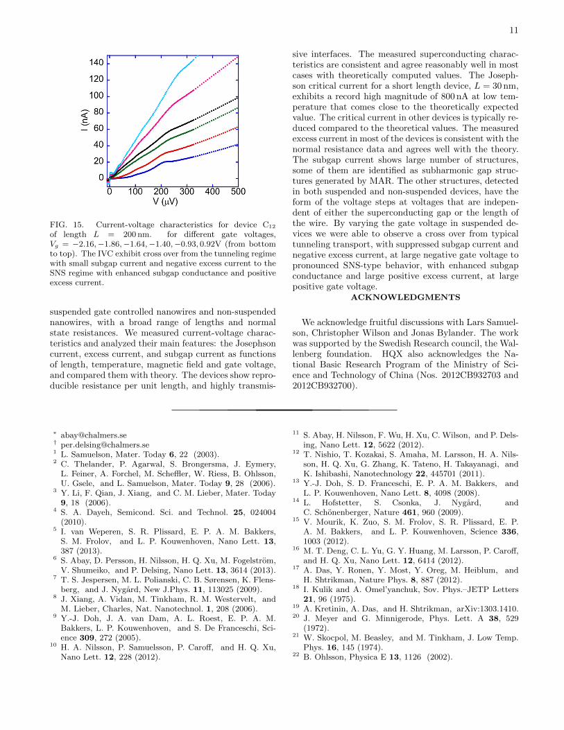
In Fig. 15a we present a set of IVCs for the suspendeddevice C12 (L ≈ 200 nm and Rn = 3.6 kΩ) for gate volt-ages ranging from Vg = −2.16V to Vg = +0.92V. Atlarge positive gate voltage, i.e. at large conductance,the IVC shows significant excess current and enhancedsubgap conductance, indicating highly transmissive SNSregime (see Fig. 15). In the opposite limit of large nega-tive gate voltage (small conductance), the IVC has a typ-ical form for SIS tunnel junctions with negative excesscurrent38 and strongly suppressed subgap conductance
FIG. 14. (a) Normal state conductance and critical currentas a function of a local-gate voltage for device C11. Afteropening of the first conducting channel at Vg ≈ −5V, theoverall conductance and critical current increase linearly withthe gate voltage. (b) IcRn product as a function of gatevoltage. The constant value indicates that the critical currentis correlated with the normal state conductance.
(Fig. 15). The suppression of the subgap conductance isexplained by small probability of MAR processes at smallvoltage, which scales with Dn, where n = 2∆/eV is thenumber of Andreev reflections. In the tunneling regimewith small D 1 the subgap conductance is exponen-tially small. At the intermediate gate voltages the deviceexhibits continuous crossover between these two regimesin accordance with the theoretical predictions for con-tacts with varying transparency.29,42
IX. CONCLUSION
We have investigated, both experimentally and theo-retically, proximity effect in InAs nanowires connectedto superconducting electrodes. We have fabricated andinvestigated a large number of nanowire devices with
11
FIG. 15. Current-voltage characteristics for device C12
of length L = 200 nm. for different gate voltages,Vg = −2.16,−1.86,−1.64,−1.40,−0.93, 0.92V (from bottomto top). The IVC exhibit cross over from the tunneling regimewith small subgap current and negative excess current to theSNS regime with enhanced subgap conductance and positiveexcess current.
suspended gate controlled nanowires and non-suspendednanowires, with a broad range of lengths and normalstate resistances. We measured current-voltage charac-teristics and analyzed their main features: the Josephsoncurrent, excess current, and subgap current as functionsof length, temperature, magnetic field and gate voltage,and compared them with theory. The devices show repro-ducible resistance per unit length, and highly transmis-
sive interfaces. The measured superconducting charac-teristics are consistent and agree reasonably well in mostcases with theoretically computed values. The Joseph-son critical current for a short length device, L = 30 nm,exhibits a record high magnitude of 800 nA at low tem-perature that comes close to the theoretically expectedvalue. The critical current in other devices is typically re-duced compared to the theoretical values. The measuredexcess current in most of the devices is consistent with thenormal resistance data and agrees well with the theory.The subgap current shows large number of structures,some of them are identified as subharmonic gap struc-tures generated by MAR. The other structures, detectedin both suspended and non-suspended devices, have theform of the voltage steps at voltages that are indepen-dent of either the superconducting gap or the length ofthe wire. By varying the gate voltage in suspended de-vices we were able to observe a cross over from typicaltunneling transport, with suppressed subgap current andnegative excess current, at large negative gate voltage topronounced SNS-type behavior, with enhanced subgapconductance and large positive excess current, at largepositive gate voltage.
ACKNOWLEDGMENTS
We acknowledge fruitful discussions with Lars Samuel-son, Christopher Wilson and Jonas Bylander. The workwas supported by the Swedish Research council, the Wal-lenberg foundation. HQX also acknowledges the Na-tional Basic Research Program of the Ministry of Sci-ence and Technology of China (Nos. 2012CB932703 and2012CB932700).
∗ [email protected]† [email protected] L. Samuelson, Mater. Today 6, 22 (2003).2 C. Thelander, P. Agarwal, S. Brongersma, J. Eymery,
L. Feiner, A. Forchel, M. Scheffler, W. Riess, B. Ohlsson,U. Gsele, and L. Samuelson, Mater. Today 9, 28 (2006).
3 Y. Li, F. Qian, J. Xiang, and C. M. Lieber, Mater. Today9, 18 (2006).
4 S. A. Dayeh, Semicond. Sci. and Technol. 25, 024004(2010).
5 I. van Weperen, S. R. Plissard, E. P. A. M. Bakkers,S. M. Frolov, and L. P. Kouwenhoven, Nano Lett. 13,387 (2013).
6 S. Abay, D. Persson, H. Nilsson, H. Q. Xu, M. Fogelstrom,V. Shumeiko, and P. Delsing, Nano Lett. 13, 3614 (2013).
7 T. S. Jespersen, M. L. Polianski, C. B. Sørensen, K. Flens-berg, and J. Nygard, New J.Phys. 11, 113025 (2009).
8 J. Xiang, A. Vidan, M. Tinkham, R. M. Westervelt, andM. Lieber, Charles, Nat. Nanotechnol. 1, 208 (2006).
9 Y.-J. Doh, J. A. van Dam, A. L. Roest, E. P. A. M.Bakkers, L. P. Kouwenhoven, and S. De Franceschi, Sci-ence 309, 272 (2005).
10 H. A. Nilsson, P. Samuelsson, P. Caroff, and H. Q. Xu,Nano Lett. 12, 228 (2012).
11 S. Abay, H. Nilsson, F. Wu, H. Xu, C. Wilson, and P. Dels-ing, Nano Lett. 12, 5622 (2012).
12 T. Nishio, T. Kozakai, S. Amaha, M. Larsson, H. A. Nils-son, H. Q. Xu, G. Zhang, K. Tateno, H. Takayanagi, andK. Ishibashi, Nanotechnology 22, 445701 (2011).
13 Y.-J. Doh, S. D. Franceschi, E. P. A. M. Bakkers, andL. P. Kouwenhoven, Nano Lett. 8, 4098 (2008).
14 L. Hofstetter, S. Csonka, J. Nygard, andC. Schonenberger, Nature 461, 960 (2009).
15 V. Mourik, K. Zuo, S. M. Frolov, S. R. Plissard, E. P.A. M. Bakkers, and L. P. Kouwenhoven, Science 336,1003 (2012).
16 M. T. Deng, C. L. Yu, G. Y. Huang, M. Larsson, P. Caroff,and H. Q. Xu, Nano Lett. 12, 6414 (2012).
17 A. Das, Y. Ronen, Y. Most, Y. Oreg, M. Heiblum, andH. Shtrikman, Nature Phys. 8, 887 (2012).
18 I. Kulik and A. Omel’yanchuk, Sov. Phys.–JETP Letters21, 96 (1975).
19 A. Kretinin, A. Das, and H. Shtrikman, arXiv:1303.1410.20 J. Meyer and G. Minnigerode, Phys. Lett. A 38, 529
(1972).21 W. Skocpol, M. Beasley, and M. Tinkham, J. Low Temp.
Phys. 16, 145 (1974).22 B. Ohlsson, Physica E 13, 1126 (2002).
12
23 H. A. Nilsson, T. Duty, S. Abay, C. Wilson, J. B. Wagner,C. Thelander, P. Delsing, and L. Samuelson, Nano Lett.8, 872 (2008).
24 D. B. Suyatin, C. Thelander, M. T. Bjork, I. Maximov,and L. Samuelson, Nanotechnology 18, 105307 (2007).
25 S. Datta, Electronic Transport in Mesoscopic Systems(Cambridge University Press, 1997).
26 P. Samuelsson, A. Ingerman, G. Johansson, E. V. Bezug-lyi, V. S. Shumeiko, G. Wendin, R. Kursten, A. Richter,T. Matsuyama, and U. Merkt, Phys. Rev. B 70, 212505(2004).
27 A. Furusaki, H. Takayanagi, and M. Tsukada, Phys. Rev.B 45, 10563 (1992).
28 G. Arnold, J. Low Temp. Phys. 68, 1 (1987).29 E. N. Bratus’, V. S. Shumeiko, and G. Wendin, Phys. Rev.
Lett. 74, 2110 (1995).30 D. Averin and A. Bardas, Phys. Rev. Lett. 75, 1831 (1995).31 J. C. Cuevas, A. Martın-Rodero, and A. L. Yeyati, Phys.
Rev. B 54, 7366 (1996).32 Cross over from diffusive short- to long-junction regime
could alternatively be modeled with a theory developed in
Ref. 38.33 J. C. Cuevas and M. Fogelstrom, Phys. Rev. B 64, 104502
(2001).34 M. Eschrig, Phys. Rev. B 80, 134511 (2009).35 A. V. Zaitsev, Sov. Phys. –JETP 59, 1015 (1984).36 V. S. Shumeiko, E. N. Bratus, and G. Wendin, Low Temp.
Phys. 23, 181 (1997).37 J. C. Cuevas, J. Hammer, J. Kopu, J. K. Viljas, and
M. Eschrig, Phys. Rev. B 73, 184505 (2006).38 E. V. Bezuglyi, E. N. Bratus’, and V. S. Shumeiko, Phys.
Rev. B 83, 184517 (2011).39 M. Y. Kupriyanov, A. Brinkman, A. A. Golubov,
M. Siegel, and H. Rogalla, Physica C 326, 16 (1999).40 G. E. Blonder, M. Tinkham, and T. M. Klapwijk, Phys.
Rev. B 25, 4515 (1982).41 V. Galaiko and N. Kopnin, in Nonequilibrium Supercon-
ductivity, edited by D. Langenberg and A. Larkin (North-Holland, Amsterdam, 1986).
42 A. Ingerman, G. Johansson, V. S. Shumeiko, andG. Wendin, Phys. Rev. B 64, 144504 (2001).


