Embed Size (px)
Citation preview
14 IEEE TRANSACTIONS ON CIRCUITS AND SYSTEMS-11: ANALOG AND DIGITAL SIGNAL PROCESSING, VOL. 43, NO. 1, JANUARY 1996
Efficient Implementation of‘ an I-Q GMSK Modulator
Alfredo Linz, Member, IEEE, and Alan Hendrickson
Abstruct- An efficient implementation of GMSK modulators achieved taking advantage of symmetry properties of the premod- ulation filter is described. The design bypasses typical processing steps such as modulating waveform ROM lookup, integration, and sinekosine ROM lookup, and therefore does not introduce the related errors. A design for a cordless telephony IC with a bit rate of 72 Kbps and 64 samples per symbol was implemented using only simple logic and 128 x 6 bits of ROM plus 2 simple 6 b +sign DAC’s.
I. INTRODUCTION
AUSSIAN MINIMUM SHIFT KEYING (GMSK) is a G frequency modulation scheme that has gained increased popularity in mobile radio communication systems, such as cordless telephony, where it is desirable to achieve narrow spectra to maximize the number of available channels, and at the same maintain low adjacent channel interference. Since the modulated signal has constant amplitude, efficient RF amplifier configurations such as class C can be used to minimize power consumption, an important consideration for battery-powered units.
Typically, the carrier frequencies for this kind of system may range from tens to thousands of MHz. This precludes on- chip generation of the final modulated signal in most presently available technologies such as a typical digital CMOS process. The method of choice is to generate equivalent baseband signals, which are then utilized by external W components. This paper describes an efficient method for generating such signals, in which errors are minimized. Part 2 briefly discusses the fundamentals of GMSK modulation. Part 3 reviews some relevant properties of Gaussian filters. Part 4 deals with the mathematical description of the frequency and phase trajectories. Part 5 describes the synthesis method of the I and Q signals. Part 6 describes the actual implementation and compares it with a conventional design. Some experimental and simulation results are given in Part 7.
11. FUNDAMENTALS OF GMSK MODULATION
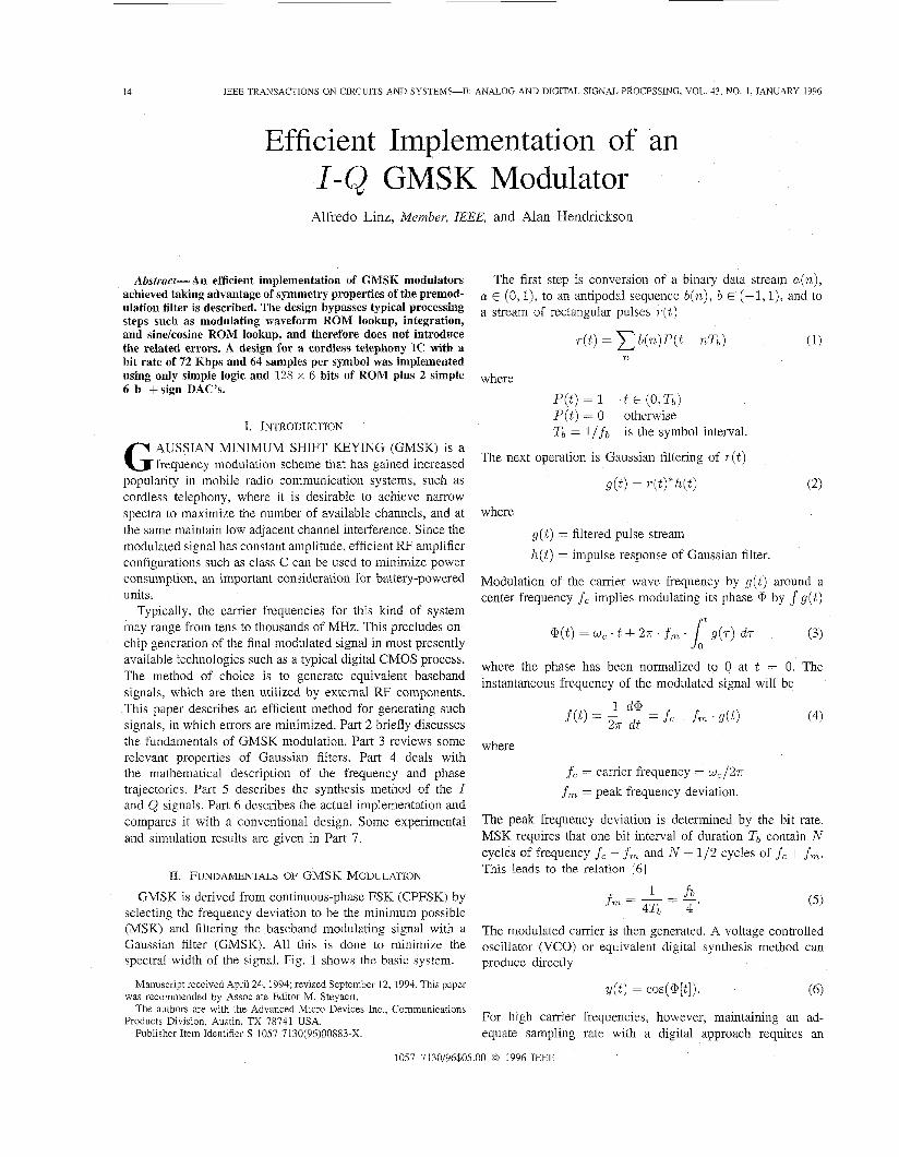
GMSK is derived from continuous-phase FSK (CPFSK) by selecting the frequency deviation to be the minimum possible (MSK) and filtering the baseband modulating signal with a Gaussian filter (GMSK). All this is done to minimize the spectral width of the signal. Fig. 1 shows the basic system.
Manuscript received April 24,1994; revised September 12,1994. Thk paper
The authors are with the Advanced Micro Devices Inc., Communications
Publisher Item Identifier S 1057-7130(96)00883-X.
was recommended by Associate Editor M. Steyaert.
Products Division, Austin, TX 78741 USA.
The first step is conversion of a binary data stream a(n), a E (0, 1), to an antipodal sequence b(n), b E (-1, 1), and to a stream of rectangular pulses ~ ( t )
T ( t ) = b(n)P(t - nTb) (1) n
where P( t ) = 1 t E (0,Tb) P ( t ) = 0 otherwise Tb = l / f b is the symbol interval.
The next operation is Gaussian filtering of ~ ( t )
S ( t ) = T(t)*h(t)
where
g ( t ) = filtered pulse stream h(t) = impulse response of Gaussian filter.
Modulation of the carrier wave frequency by g ( t ) around a center frequency f c implies modulating its phase @ by g ( t )
where the phase has been normalized to 0 at t = 0. The instantaneous frequency of the modulated signal will be
(4)
where
f c = carrier frequency = wc/2n f m = peak frequency deviation.
The peak frequency deviation is determined by the bit rate. MSK requires that one bit interval of duration Tb contain N cycles of frequency f c - f m and N + l / 2 cycles of f c + f m . This leads to the relation 161
4Tb 4 ’ (5)
The modulated carrier is then generated. A voltage controlled oscillator (VCO) or equivalent digital synthesis method can produce directly
y ( t ) = C O S ( q t 1 ) . (6)
For high carrier frequencies, however, maintaining an ad- equate sampling rate with a digital approach requires an
1057-7130/96$05.00 0 1996 IEEE
1s LINZ AND HENDRICKSON: I-Q GMSK MODULATOR
j Gausslan a(n)
finer + P(t)
8 0) V(t) cos + total power at the output of the filter can be found from H(w). % I -
I ( t ) and Q ( t ) can be written as Normalized 3 dB Bandwidth: This is defined as
I ( t ) = Re{ exp [j27r fm I’ g ( 7 ) d ~ ] } = Re{u(t)}
Q(t) = Im{u(t)} (9)
where u(t) is a complex phase function. The argument of the I ( t ) and Q(t ) signals varies much more
slowly than (a(t), and this makes it feasible to generate I and Q digitally. After conversion to the analog domain, the final signal y(t) can be generated using a suitable mixer.
In a conventional implementation, the steps outlined in Fig. 1 are followed literally; the filtered data g ( t ) are generated first, either using an actual filter that approximates the Gaussian characteristic or, more efficiently, using ROM table lookup methods. Integration of g ( t ) is done in a “phase accumulator,” and the cosine and sine are obtained from a sine ROM, using the accumulator value as an address.
In our implementation, these steps are skipped, and the I and Q signals are generated directly from the binary data, thereby eliminating the errors in filtering, phase truncation and sinekosine computation inherent in the conventional architec- ture.
where Bb = B s d ~ / 2 ~ and T 1 T b = 1/ fb. BbT is a common design parameter. The parameter a can be found from B6T from the following relationship
Normalized Noise Bandwidth: This is defined as the noise bandwidth divided by the bit rate f b of the system
Some workers use BNT instead of BbT as a design parameter. The two are related by (14). The parameter Q can be found from BNT from the following relationship
To develop the method, we use some properties of Gaussian Impulse Response: The following functions form a Fourier filters described in the next section.
Transform pair
111. PROPERTIES OF THE GAUSSIAN FILTER e-atz c--) E e - g . (17) In this section we review some important properties and
parameters of a Gaussian filter. For more detail, please see [I]. Comparing the RHS with (10) and recalling that the complex
exponential factor is equivalent to a time shift, one can obtain Transfer Function:
A H ( w ) - Aoe-aw2e--3wto (10) h(t) = ~ - 1 { ~ ( w ) ) = ope-[ ( t - to)p12 (18) &f
The system has linear phase, with group delay to . The param- eter a defines the bandwidth. where
3 dB Bandwidth:
@I (11) = p B n IT = 2 6 f b ( B ~ T ) = @Tfb(BbT) . (19) B 3 d B =
This is the frequency at which IH(w)I is 0.707Ao. Note that h(t) is symmetric around t = t o .
16 IEEE TRANSACTIONS ON CIRCUITS AND SYSTEMS-D: ANALOG AND DIGITAL SIGNAL PROCESSING, VOL. 43, NO. 1, JANUARY 1996
n d e X
om W1
a ( t ) = * + lom h(r) dr . (20) 2
Equabon Cmmenls
foe ) = -1 fa(‘ 1 = -f,O 1 f i ( t )=- f s ( t ) f; (f ) = e& [ t - T,])
Here, A0 is the value of the magnitude of H ( w ) at w = 0.
A0 a( t ) = -[I 2 + erf(P[t - t o ] ) ]
010 f 2 ( t ) = e& t ) - e r f ( P [ ~ - T ~ ] ) - I
01 I f , ( t )= d B f 1
(u,-~, u,,a,+l), it can be shown that this is equivalent to dx = -erf(-z). (22)
Note that a ( t ) is symmetric in the following sense
to + T ) + to - 7 ) = A0 (23)
This follows from (21) and (22). Response to a Pulse: Since a pulse can be expressed as the
difference of two step functions and the filter is a linear system, the response p ( t ) to a pulse P( t ) of duration Tb can be found to be
Response to a Pulse Train: Linearity also allows US to ap- ply superposition to find the response to a train of NRZ pulses of the form of (1). We express the response to a pulse train varying from -A0 to A0 as the response to a pulse train varying from 0 to 2Ao plus a constant of value -A0
g ( t ) = AO a(n){erf[p(t - t o - nTb)] n
- erf[p(t -
From this point on, we make Ao = 1 without loss of generality. This means g ( t ) has a maximum peak value of 1, which in tum means that f ( t ) varies from f c - f, to f c + f, according to (4).
Iv . FREQUENCY AND PHASE TF&JFKTORIES
Equation (24) shows that the pulse response extends theo- retically from --oo to $00, so the response to a pulse train inside a given symbol interval has interference from all past and future symbols. In practice, however, the extent of the pulse response is usually considered limited to only the two nearest neighbors, and this is reflected in the fact that only three consecutive bits are used at a time. This approximation has been used even for BbT = 0.3 [8] and it is equivalent to multiplying the actual pulses by a rectangular one of duration 3Tb. Values of BbT significantly lower than this limit result in more appreciable interference from the second- nearest neighbors and more difficulty in achieving reliable demodulation due to eye closure, so practical systems tend to use values of BbT as large as possible.
If we impose the condition that the response within a symbol interval (mTb,mTb + Tb) be dependent only on
requiring that
erf(Pz) M 1 for 1x1 2 Tb. (26)
erf(p Tb) 1 (27)
pTb = 2&(BbT) (28)
In particular, this implies
where
For example, BbT = 0.3 results in a 2.4% error in (27), while BbT = 0.337 gives a 1% error and BbT = 0.452 results in 0.1% error. A value of BbT = 0.7, which is used in our application, gives negligible deviation.
If (27) is true, then the response in the interval considered can be expressed as
gm(t) am-1[1 - erf(Dt)l + am[erf(Pt) - erf(p[t - Tb])] + am+l[I + erf(p(t - 1.
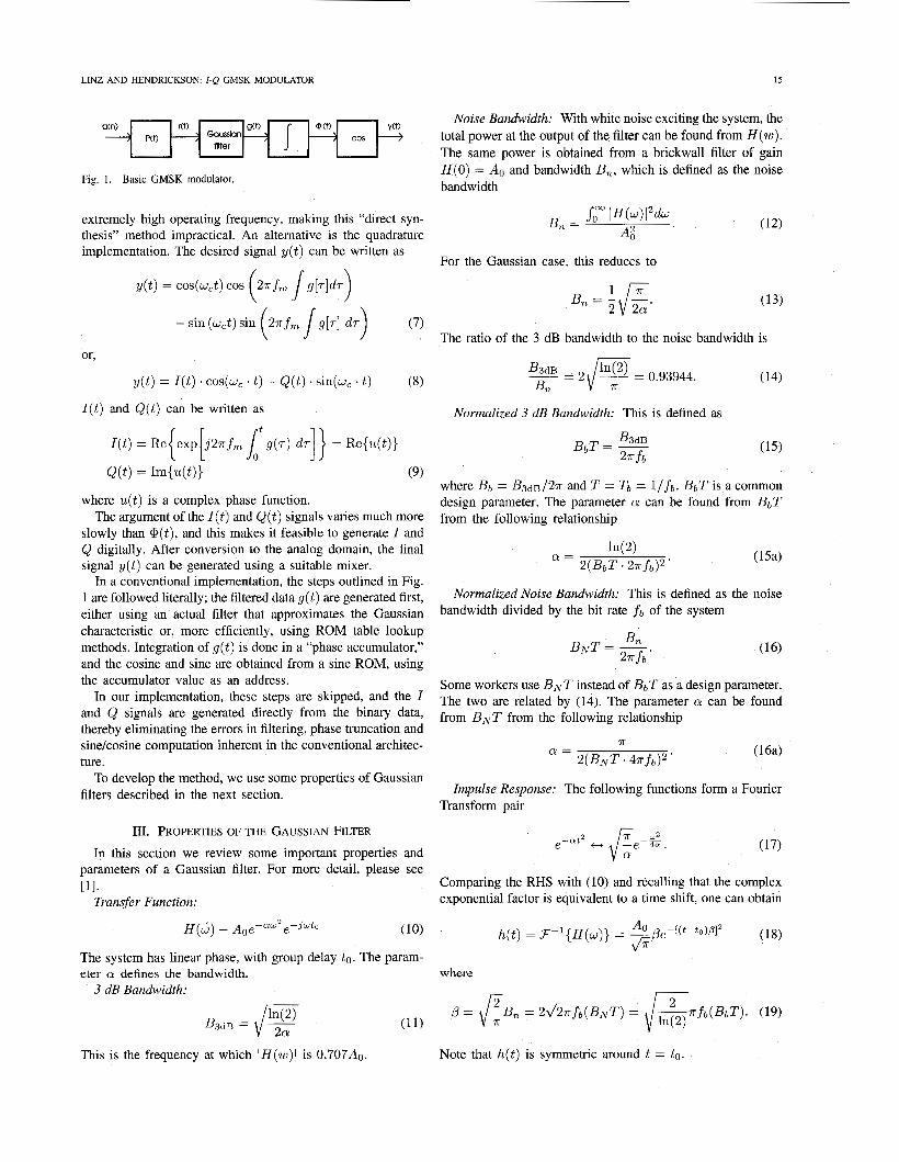
A. Frequency Trajectories As the pulses can have one of two possible polarities
(a , = 0 or l), we can have 23 = 8 possible curves. Since the frequency of the modulated signal has to be proportional to g ( t ) [see (4)], the curves are called “frequency trajectories”.
Equations for the trajectories can be obtained from (29) substituting particular values for the a,.
We can show that there are only three independent frequency trajectories, from which the remaining 5 can be obtained by means of simple operations, provided (27) is met.
The concept of frequency trajectory allows us to express the modulating signal g ( t ) as a train of baseband pulses, as follows
g ( t ) = f i (n) ( t - n ~ ) ~ ( t - n ~ ) (30) n
where Z(n) = 4an-l + 2an + an+l is the index of the trajectory. The equations for the 8 paths are given in Table I
Trajectories 2, 3, and 7 are calculated first. The remaining can be found from f 2 , f 3 , and f7 as follows, provided (27) holds. First, trajectories corresponding to complemented triplets are just the negative of the trajectory corresponding to the original triplet (un-l , a,, an+l). Trajectories 0, 5, and 4
LINZ AND HENDRICKSON I-Q GMSK MODULATOR
Frequency Trajectories for BbT = 0.337
I 111l I 1
. . . . . . . . . . . - . . I $ 0
1
/ -
17
To find the value of u(t) in the interval (nT, [n + 112') we first separate the integral
The first integral in the exponent is evaluated over an integer number of symbol intervals, and is just the cumulative sum of phase changes up to time nT
~
where u(t) is defined in (9). Since all frequency trajectories can be expressed in terms of
0 TI2 1
time
Fig. 2. Frequency trajectories for BbT = 0.337.
Fmque~y Traptones IW BbT = 0 7
I
where @ l ( k ) is the incremental change in phase over the interval ( k - l)T <= t < k T , and depends on the particular frequency trajectory in that interval, f l ( k ) , where
Z(k) E {0,1,. . . ,7}. (34)
The phase u(t) in the interval (nT, [n+l]T), which we denote as un(t), can then be expressed as 111,110 011,111 lI7T 010,011 010,110
111,110 011,111 1
0 i - - - - - -
1
un(t) = exp{j@,}exp { j2n f m l;+t"(r) d r } (35)
and the total complex phase function can be written as
u(t) =
2 exp{ j [.. + 2n f m n=--03
I I 1 000,001 000,100
I
0 TI2 T
time
Fig. 3. Frequency trajectories for BbT = 0.7.
are obtained in this way. Trajectories corresponding to time- reversed triplets are also time-reversed in the sense explained in the table comments. This applies to trajectories 6 and 1.
All frequency trajectories can be obtained from f i , f 3 ,
and f7 by sign change andor time reflection. The frequency trajectories obtained from these equations are shown in Figs. 2 and 3 for two different values of BbT.
B. Phase Trajectories The complex phase function u(t) can be expressed as a train
of baseband pulses, in much the same way as is done with a simple FSK signal [ 3 ] .
u(t) = un(t - nT)P(t - nT) (31) n
From (31), (36) it follows that
where $qn)(t) will be called a "phase trajectory"
Here qhZ(O) is the initial phase value On. which depends on the position of the trajectory in time, or equivalently, on the history of the sequence a(m) . The time-varying component $:(t) depends only on the frequency trajectory during the interval under consideration and is not otherwise dependent on the history of a(m) .
To determine the $z (O), we need the phase change over one complete symbol interval, defined to be consistent with (33) as
18 E E E TRANSACTIONS ON CIRCUITS AND SYSTEMS-II. ANALOG AND DIGITAL SIGNAL PROCESSING, VOL 43, NO 1, JANUARY 1996
TABLE 11
I /
erf(z), the following integral is useful ([4])
special cases of interest are
We are concerned with the case where erf(pz) - 1 (26). One can make use of the following asymptotic expansion ( [ 5 ] ) for positive z
to show that in that case (33) is approximately equal to
With these definitions, we proceed to find the time-varying components of the phase trajectories and the total phase change over a symbol interval. The validity of (27) is assumed throughout. After considering one trajectory in some detail, we summarize them in Table 11.
Trajectory for (010):
&(t) ~ ~ I ( ~ , ~ ) - I I ( ~ , O ) -Il(P,t-Tb)+Tb-t. (44)
Final Value
Ths 3 Pnnoipal Phass Trqectones
d2
d2-2A
B
8 a
d2 - 4A
0 TI2 T
time
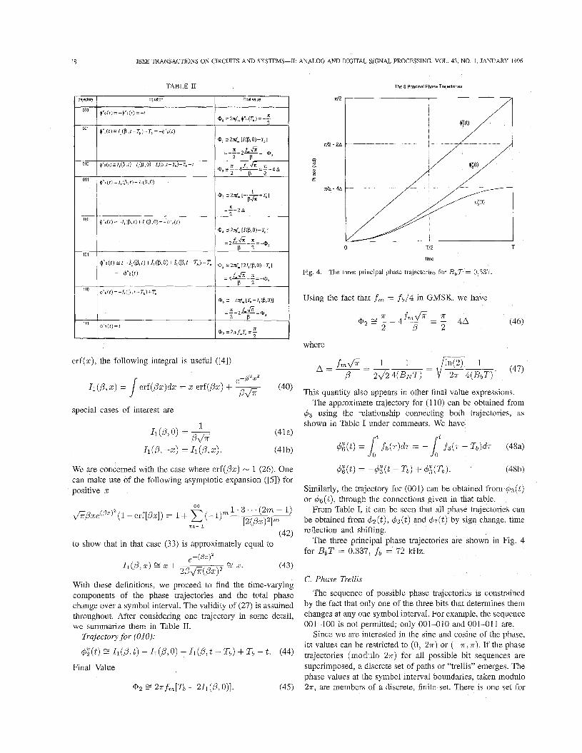
Fig 4. The three principal phase trajectories for BbT = 0.337.
Using the fact that f m = f b /4 in GMSK, we have
where
This quantity also appears in other final value expressions. The approximate trajectory for (1 10) can be obtained from
4 3 using the relationship connecting both trajectories, as shown in Table I under comments. We have
$g(t) = f fG('T)d'T = - f3(T - Tb)d7 (48a)
4g(t) = -&(t - Tb) f dy(Tb). (48b)
Similarly, the trajectory for (001) can be obtained from $3(t) or 4 6 ( t ) , through the connections given in that table.
From Table I, it can be seen that all phase trajectories can be obtained from 4 2 ( t ) , 4 3 ( t ) and 47 (t) by sign change, time reflection and shifting.
The three principal phase trajectories are shown in Fig. 4 for BbT = 0.337, f b = 72 k H Z .
0 1
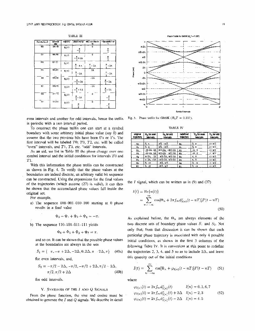
C. Phase Trellis The sequence of possible phase trajectories is constrained
by the fact that only one of the three bits that determines them changes at any one symbol interval. For example, the sequence 001-100 is not permitted; only 001-010 and 001-01 1 are.
Since we are interested in the sine and cosine of the phase, its values can be restricted to (0 , 27r) or ( - 7 r > 7 r ) . If the phase trajectories (modulo 27r) for all possible bit sequences are superimposed, a discrete set of paths or "trellis" emerges. The phase values at the symbol interval boundaries, taken modulo 2n, are members of a discrete, finite set. There is one set for
LINZ AND HENDRICKSON: I-Q GMSK MODULATOR
TABLE I11
19
Phase Trellis for GMSK (BbT = 0 337)
0 1 2
Symbol Intervals
even intervals and another for odd intervals, hence the trellis is periodic with a two interval period.
boundary with some arbitrary initial phase value (say 0) and assume that the two previous bits have been 0's or 1's. The first interval will be labeled TO; TO, T 2 , etc. will be called "even" intervals, and 2'1, T3, etc. "odd" intervals.
As an aid, we list in Table 111 the phase change over one symbol interval and the initial conditions for intervals TO and T1.
With this information the phase trellis can be constructed as shown in Fig. 4. To verify that the phase values at the boundaries are indeed discrete, an arbitrary valid bit sequence
Fig. 5. Phase for GMSK (BbT = 0.337)
To construct the phase trellis one can start at a symbol TABLE IV
can be constructed. Using the expressions for the final values of the trajectories (which assume (27) is valid), it can then the I signal, which can be written as in (9) and (37)
be shown that the accumulated phase values fall inside the original set. I ( t ) = Re{u(t)}
Y 00
For example, = COS[@, + 2 ~ f ~ 4 ; ( , 1 ( t - nT)]P(t - nT) a) The sequence 000-001-010-100 starting at 0 phase n=-m
(50) results in a final value
a0 + a1 + a2 +a4 = -7r. As explained before, the 0, are always elements of the
b) The sequence 110-101-01 1-1 11 yields two discrete sets of boundary phase values SI and S2. Not only that: from that discussion it can be shown that each particular phase trajectory is associated with only 4 possible
and SO on. It Can be shown that the Possible Phase values at the boundaries are always in the sets
SI = {-n, -n + 2 A , -2A, 0,28,7r - 2 8 , 7 r }
for even intervals, and,
initial conditions, as shown in the first 3 columns of the following Table IV. It is convenient at this point to redefine the trajectories 2, 3, 4, and 5 so as to include 2 8 , and leave this quantity out of the initial conditions
(49a)
for odd intervals. where
(Pl(n) ( t ) = 2"fm4;(,) ( t )
(Pl(n)@) = 2wfm@(,)(t) - 2A
l(n) = 0,1 ,6 ,7 v. SYNTHESIS OF THE I AND Q SIGNALS (Pl( , ) ( t ) = 2TL4;(,,(t) + 2 A l(n) = 273 (52) From the phase function, the sine and cosine must be
obtained to generate the I and Q signals. We describe in detail = 4,
20 IEEE TRANSACTIONS ON CIRCUITS AND SYSTEMS-II ANALOG AND DIGITAL SIGNAL PROCESSING, VOL 43, NO. 1, JANUARY 1996
and
Q n = 0, l(n) = 0, I, 6,7 qn = on - 2a qn) = 2 , 3 (53) Q, = 0, + 2A Z(n) = 4,5
as shown in the last 3 columns of Table IV To generate I ( t ) and Q(t ) , the cosine and sine of the above
(redefined) trajectories must be obtained. At first sight, it would appear that a large number of curves must be generated. This is not so, however. First, the bottom 4 curves and their initial conditions are just the negatives of the upper 4. This cuts the number of curves by half. We choose 1, 2, 3, and 7 .
Second, we saw that trajectory 1 can be obtained from trajectory 3. In terms of redefined trajectories we get
~ ( t ) = ~ 3 ( t - Tb) - 2A + 2rfm&(Tb) = ~ 3 ( T b - t ) - - 2 (54)
7r
or
( P 3 ( t ) = ( P l ( T b - t ) + '.
cos[p3(t)l = cos ' p I ( ~ b - t ) + -1 = - sin[cpl(Tb - t)l
(544 2
For the cosine of 43(t) we have, for example, ,Tr
2 (55)
This is the time reversed and inverted version of the sine of trajectory 1. A similar relationship holds for the sine. Thus, only the sine and cosine of trajectory 1 (or 3) are needed.
Further reductions come about in virtue of symmetries in the redefined trajectories, of which 2 and 7 satisfy the following relationship
[ = - sin[pl(t)It+Tb-t*
i = 2,7 (56)
for some choice of sign. This condition guarantees that
cos(pi[t]) = sin((oi[Tb - t]) i = 2,7. (57)
Basic CUNSS for BbT = 0 337
1 .o
8
6
e
4
0 TI2 T
t"
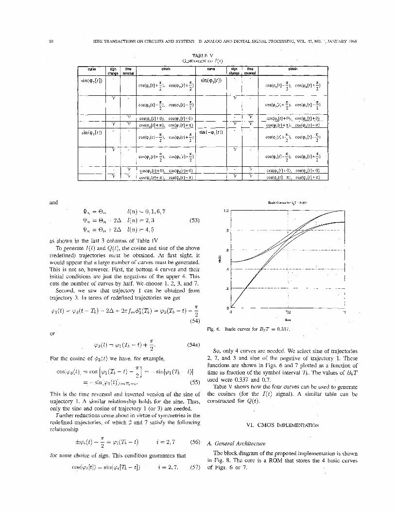
Fig. 6. Basic curves for BbT = 0.337.
So, only 4 curves are needed. We select sine of trajectories 2, 7, and 3 and sine of the negative of trajectory 1. These functions are shown in Figs. 6 and 7 plotted as a function of time as fraction of the symbol interval T b . The values of BbT used were 0.337 and 0.7.
Table V shows how the four curves can be used to generate the cosines (for the I(d) signal). A similar table can be constructed for Q(t).
VI. CMOS IMPLEMENTATION
A. General Architecture
The block diagram of the proposed implementation is shown in Fig. 8. The core is a ROM that stores the 4 basic curves of Figs. 6 or 7 .
21 LINZ AND HENDRICKSON I-Q GMSK MODULATOR
Baslo CUNWS for q T = 0 7
1 .a
.a
.6 - t
.4
2
0 0 Ti2
time
Fig. 7. Basic curves for BbT = 0.7.
?
m ICOUMER I I
I
B A N K ' / -
/ L4TCH zy / / LATCH
-L] GENERATOW 1 ROM
8 - SAMPLE , INDEX CoSPO~Rlpl I.
cos@t)
Fig. 8. New synthesizer architecture.
B. Look-Up ROM
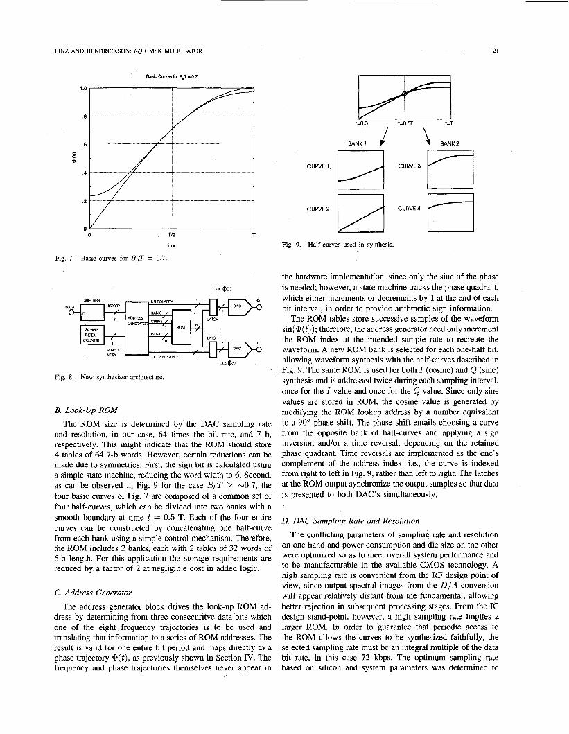
The ROM size is determined by the DAC sampling rate and resolution, in our case, 64 times the bit rate, and 7 b, respectively. This might indicate that the ROM should store 4 tables of 64 7-b words. However, certain reductions can be made due to symmetries. First, the sign bit is calculated using a simple state machine, reducing the word width to 6. Second, as can be observed in Fig. 9 for the case BbT 2 -0.7, the four basic curves of Fig. 7 are composed of a common set of four half-curves, which can be divided into two banks with a smooth boundary at time t = 0.5 T. Each of the four entire curves can be constructed by concatenating one half-curve from each bank using a simple control mechanism. Therefore, the ROM includes 2 banks, each with 2 tables of 32 words of 6-b length. For this application the storage requirements are reduced by a factor of 2 at negligible cost in added logic.
C. Address Generator
The address generator block drives the look-up ROM ad- dress by determining from three consecuritve data bits which one of the eight frequency trajectories is to be used and translating that information to a series of ROM addresses. The result is valid for one entire bit period and maps directly to a phase trajectory @(t) , as previously shown in Section IV. The frequency and phase trajectories themselves never appear in
t 4 . O
BANK 1
CURVE 1
t4.5T t=T
BANK 2
CURVE 3
Fig. 9. Half-curves used in synthesis.
the hardware implementation, since only the sine of the phase is needed; however, a state machine tracks the phase quadrant, which either increments or decrements by 1 at the end of each bit interval, in order to provide arithmetic sign information.
The ROM tables store successive samples of the waveform sin( @ ( t ) ) ; therefore, the address generator need only increment the ROM index at the intended sample rate to recreate the waveform. A new ROM bank is selected for each one-half bit, allowing waveform synthesis with the half-curves described in Fig. 9. The same ROM is used for both I (cosine) and Q (sine) synthesis and is addressed twice during each sampling interval, once for the 1 value and once for the Q value. Since only sine values are stored in ROM, the cosine value is generated by modifying the ROM lookup address by a number equivalent to a 90" phase shift. The phase shift entails choosing a curve from the opposite bank of half-curves and applying a sign inversion and/or a time reversal, depending on the retained phase quadrant. Time reversals are implemented as the one's complement of the address index, i.e., the curve is indexed from right to left in Fig. 9, rather than left to right. The latches at the ROM output synchronize the output samples so that data is presented to both DAC's simultaneously.
D. DAC Sampling Rate and Resolution
The conflicting parameters of sampling rate and resolution on one hand and power consumption and die size on the other were optimized so as to meet overall system performance and to be manufacturable in the available CMOS technology. A high sampling rate is convenient from the RF design point of view, since output spectral images from the D / A conversion will appear relatively distant from the fundamental, allowing better rejection in subsequent processing stages. From the IC design stand-point, however, a high sampling rate implies a larger ROM. In order to guarantee that periodic access to the ROM allows the curves to be synthesized faithfully, the selected sampling rate must be an integral multiple of the data bit rate, in this case 72 kbps. The optimum sampling rate based on silicon and system parameters was determined to
22 IEEE TRANSACTIONS ON CIRCUITS AND SYSTEMS-II: ANALOG AND DIGITAL SIGNAL PROCESSING, VOL. 43, NO. 1, JANUARY 1996
-80
DATA
(72 kbis)
1 " " I ' " " " " ' " '
0 5x10⁵ I 0x105 1 5x10⁵ 2 0x1 o5
frequency trajsctary $-h PHASE
truncated
18
Fig. 10. Typical conventional synthesizer architecture
Example I (or Q) Waveforms
I ' ' ' ' " ' " ~
I B,T=0337 , I
BbT=0.7 ,
I I I . . , . t . . , . I . . . I I
1000 2000 3000 4wo
sample number (64 samples I symbol Interval)
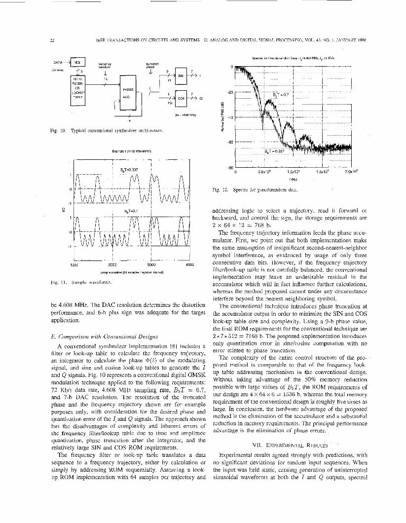
Fig. 11. Sample waveforms.
be 4.608 MHz. The DAC resolution determines the distortion performance, and 6-b plus sign was adequate for the target application.
E. Comparison with Conventional Designs A conventional synthesizer implementation [ 81 includes a
filter or look-up table to calculate the frequency trajectory, an integrator to calculate the phase @(t) of the modulating signal, and sine and cosine look-up tables to generate the I and Q signals. Fig. 10 represents a conventional digital GMSK modulation technique applied to the following requirements: 72 Kb/s data rate, 4.608 MHz sampling rate, &,T = 0.7, and 7-b DAC resolution. The resolution of the truncated phase and the frequency trajectory shown are for example purposes only, with consideration for the desired phase and quantization error of the I and Q signals. The approach shown has the disadvantages of complexity and inherent errors of the frequency filterflookup table due to time and amplitude quantization, phase truncation after the integrator, and the relatively large SIN and COS ROM requirements.
The frequency filter or look-up table translates a data sequence to a frequency trajectory, either by calculation or simply by addressing ROM sequentially. Assuming a look- up ROM implementation with 64 samples per trajectory and
Spedra far Pseudo-random Data - fe=4.M)8 MHz. f,=72 Kh/s
' ~ " ~ ' ~ ' " " " ~ '
,
........
. . . . . . . . . . . . . . . I.. . ........
. . . . . . . . . . . . . ..'bT.= O'
addressing logic to select a trajectory, read it forward or backward, and control the sign, the storage requirements are 2 x 64 x 12 = 768 b.
The frequency trajectory information feeds the phase accu- mulator. First, we point out that both implementations make the same assumption of insignificant second-nearest-neighbor symbol interference, as evidenced by usage of only three consecutive data bits. However, if the frequency trajectory filterfiook-up table is not carefully balanced, the conventional implementation may leave an undesirable residual in the accumulator which will in fact influence further calculations, whereas the method proposed cannot under any circumstance interfere beyond the nearest neighboring symbol.
The conventional technique introduces phase truncation at the accumulator output in order to minimize the SIN and COS look-up table size and complexity. Using a 9-b phase value, the final ROM requirements for the conventional technique are 2 * 7 * 512 = 7168 b. The proposed implementation introduces only quantization error in sinelcosine computation with no error related to phase truncation.
The complexity of the entire control structure of the pro- posed method is comparable to that of the frequency look- up table addressing mechanism in the conventional design. Without taking advantage of the 50% memory reduction possible with large values of BbT, the ROM requirements of our design are 4 x 64 x 6 = 1536 b, whereas the total memory requirement of the conventional design is roughly five times as large. In conclusion, the hardware advantage of the proposed method is the elimination of the accumulator and a substantial reduction in memory requirements. The principal performance advantage is the elimination of phase errors.
VII. EXPERIMENTAL RESULTS
Experimental results agreed strongly with predictions, with no significant deviations for random input sequences. When the input was held static, causing generation of uninterrupted sinusoidal waveforms at both the I and Q outputs, spectral
LINZ AND HENDRICKSON I-Q GMSK MODULATOR 23
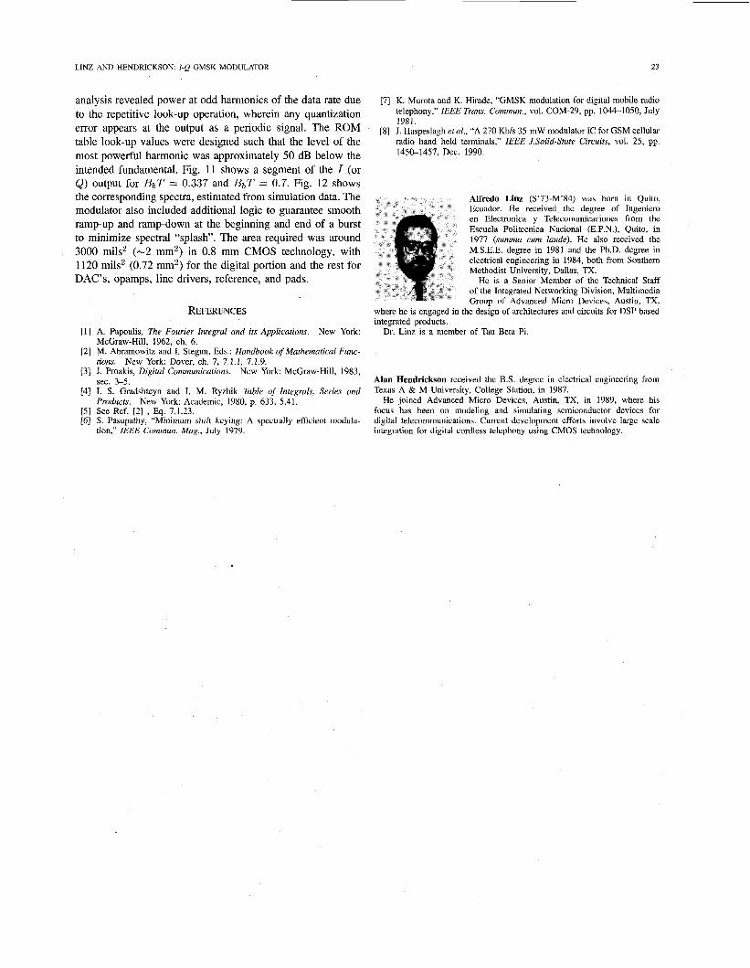
analysis revealed power at odd harmonics of the data rate due to the repetitive look-up operation, wherein any quantization error appears at the output as a periodic signal. The ROM table look-up values were designed such that the level of the most powerful harmonic was approximately 50 dB below the intended fundamental. Fig. 11 shows a segment of the I (or Q) output for BbT = 0.337 and BbT = 0.7. Fig. 12 shows the corresponding spectra, estimated from simulation data. The modulator also included additional logic to guarantee smooth ramp-up and ramp-down at the beginning and end of a burst to minimize spectral “splash”. The area required was around 3000 mils2 (-2 mm2) in 0.8 mm CMOS technology, with 1120 mils2 (0.72 mm2) for the digital portion and the rest for DAC’s, opamps, line drivers, reference, and pads.
REFERENCES
[ l ] A. Papoulis, The Fourier Integral and its Applications. New York McGraw-Hill, 1962, ch. 6.
[2] M. Abramowitz and I. Stegun, Eds.: Handbook of Mathematical Func- tions. New York: Dover, ch. 7, 7.1.1, 7.1.9.
[3] J. Proakis, Digital Communications. New York McGraw-Hill, 1983, sec. 3-5.
[4] I. S. Gradshteyn and I. M. Ryzhik Table of Integrals, Series and Products. New York: Academic. 1980. D. 633. 5.41.
[5] See Ref. 121 , Eq. 7.1.23. [6] S. Pasupathy, “Minimum shift keying: A spectrally efficient modula-
tion,’’ IEEE-Commun. Mag., July -1979.
[7] K. Murota and K. Hirade, “GMSK modulation for digital mobile radio telephony,” IEEE Trans. Commun., vol. COM-29, pp. 1044-1050, July 1981.
[8] J. Haspeslagh et al., “A 270 Kbls 35-mW modulator IC for GSM cellular radio hand held terminals,” IEEE JSolid-State Circuits, vol. 25, pp. 1450-1457, Dec. 1990.
Alfredo Linz (S’73-M’84) was born in Quito, Ecuador. He received the degree of Ingeniero en Electronica y Telecomunicaciones from the Escuela Politecnica Nacional (E.P.N.), Quito, in 1977 (summa cum laude). He also received the M.S.E.E. degree in 1981 and the Ph.D. degree in electrical engineering in 1984, both from Southern Methodist University, Dallas, TX.
He is a Senior Member of the Technical Staff of the Integrated Networking Division, Multimedia Group of Advanced Micro Devices, Austin, TX,
where he is engaged in the design of architectures and circuits for DSP based integrated products.
Dr. Linz is a member of Tau Beta Pi.
Alan Hendrickson received the B.S. degree in electrical engineering from Texas A & M University, College Station, in 1987.
He joined Advanced Micro Devices, Austin, TX, in 1989, where his focus has been on modeling and simulating semiconductor devices for digital telecommunications. Current development efforts involve large scale integration for digital cordless telephony using CMOS technology.