Embed Size (px)
Citation preview
European Patent Office ^ ̂ ̂ ^ I ̂ ̂ ̂ ̂ ̂ ̂ II ̂ ̂ ̂ II ̂ ̂ ̂ ̂ ̂ II ̂ ̂ ̂ ̂ ̂ I ̂
Office europeen des brevets £ P Q 3 3 3 1 8 4 A 1
EUROPEAN PATENT A P P L I C A T I O N
(43) Date of publication: (51) |nt CI G02B 27/00, H04N 13 /00 01.04.1998 Bulletin 1998/14
(21) Application number: 97307610.2
(22) Date of filing: 26.09.1997
(84) Designated Contracting States: • Moseley, Richard Robert AT BE CH DE DK ES Fl FR GB GR IE IT LI LU MC Littlemore, Oxford OX4 45LZ (GB) NL PT SE • Ezra
Wallingford, Oxfordshire OX10 0RL (GB) (30) Priority: 30.09.1996 GB 9620392 • Harrold, Jonathan
Sandford-on-Thames, Oxford OX4 4XS (GB) (71) Applicant: SHARP KABUSHIKI KAISHA
Osaka 545 (JP) (74) Representative: Robinson, John Stuart Marks & Clerk
(72) Inventors: Nash Court • Woodgate, Graham John Oxford Business Park South
Henley-on-Thames, Oxfordshire RG9 1TD (GB) Oxford OX4 2RU (GB)
(54) Spatial light modulator with horizontally overlapping pixels
(57) A spatial light modulator comprises a plurality are overlapping regions (13) and non-overlapping re- of picture elements arranged as rows and columns. The gions (12). The vertical extent of each picture element columns are arranged as adjacent groups, for instance is substantially constant throughout the non-overlap- for association with an element of a parallax device to ping region (12) and is substantially equal to the sum of provide an autostereoscopic 3D display. Adjacent pic- the heights of the adjacent picture elements throughout ture elements disclosed in each row and in adjacent col- the overlapping regions (1 3). The overlapping regions umns of each group overlap horizontally so that there may be of right-angled triangular shape.
F IG 5a
<
00
a . LU
Printed by Jouve, 75001 PARIS (FR) (Cont. next page)
EP0 833 184 A1
F I G S b
2
1 EP0 833 184 A1 2
Description
The present invention relates to a spatial light mod- ulator (SLM) and to a directional display. The directional display may, for instance, be a three dimensional (3D) s autostereoscopic display.
The term "spatial light modulator" as used herein is defined to include not only devices which modulate light from an external light source but also devices which emit light of a modulatable intensity. 10
EP 0 625 861 discloses an SLM having a picture element (pixel) pattern which is suitable for generating contiguous viewing windows when used in an autoster- eoscopic display. For instance, when used with a paral- lax device such as a parallax barrier or lenticular screen, 15 there is a smooth transition from one view to another when an observer moves laterally with respect to the display. In particular, undesirable black band features and image intensity modulation are reduced or eliminat- ed. Such a display is suitable for tracking the movement 20 of an observer electronically so as to increase the ob- server viewing freedom while perceiving the 3D effect. Suitable lateral and longitudinal tracking techniques are disclosed in EP 0 726 482 and EP 0 721 131. Further, a technique for manufacturing an SLM of this type is dis- 25 closed in GB 2 302 978 and EP 0 752 609. GB 2 309 609 and EP 0 786 912 discloses an SLM having a dif- ferent pixel pattern. In this case, adjacent pixels overlap horizontally so that, when used in an autostereoscopic 3D display, the viewing windows overlap laterally. This 30 type of display is also suitable for providing electronic tracking of an observer.
EP 0 404 289 discloses an autostereoscopic 3D dis- play comprising a flat display panel associated with a lenticular screen employing pitch changes and thick- 35 ness changes. Tracking of the position of an observer so that viewing windows follow the observer is achieved by moving the lenticular screen laterally and longitudi- nally with respect to the display panel.
EP 0 354 851 discloses an autostereoscopic 3D dis- 40 play in which an image source is located behind a len- ticular screen. In order to provide observer tracking, the image information supplied to the image source pixels is changed in accordance with the observer position so as to keep the observer in the correct stereoscopic zone 45 while permitting movement.
J.B. Eichenlaub, "An Autostereoscopic Display with High Brightness and Power Efficiency", SPIE Vol. 2177, 4-15(1 994) discloses a rear illumination of the autoster- eoscopic display in which a set of optics produces a set so of thin vertical light lines behind an SLM. These light lines co-operate with the pixel apertures of the SLM to provide directional illumination. Observer tracking is achieved by moving the positions of the light lines rela- tive to the SLM. The light lines are produced by imaging 55 a light source through a lenticular screen to provide ver- tical thin bright images on a diffuser, which images act as thin strip sources of nondirectional light. Several light
sources are provided and, by switching between the dif- ferent light sources, the images on the diffuser change position so as to simulate a moving light source.
C. Van Berkel, D.W. Parker, A.R. Franklin, "Multi- View 3D-LCD", IS&T/SPIE Symposium on Electronic Imaging: Stereoscopic Displays and Applications VIII, (San Jose, USA, 1996) disclose an autostereoscopic display comprising a liquid crystal device (LCD) dis- posed behind a lenticular screen. The LCD is of a stand- ard type but has a relatively high aperture ratio (ratio of total pixel area to panel area).
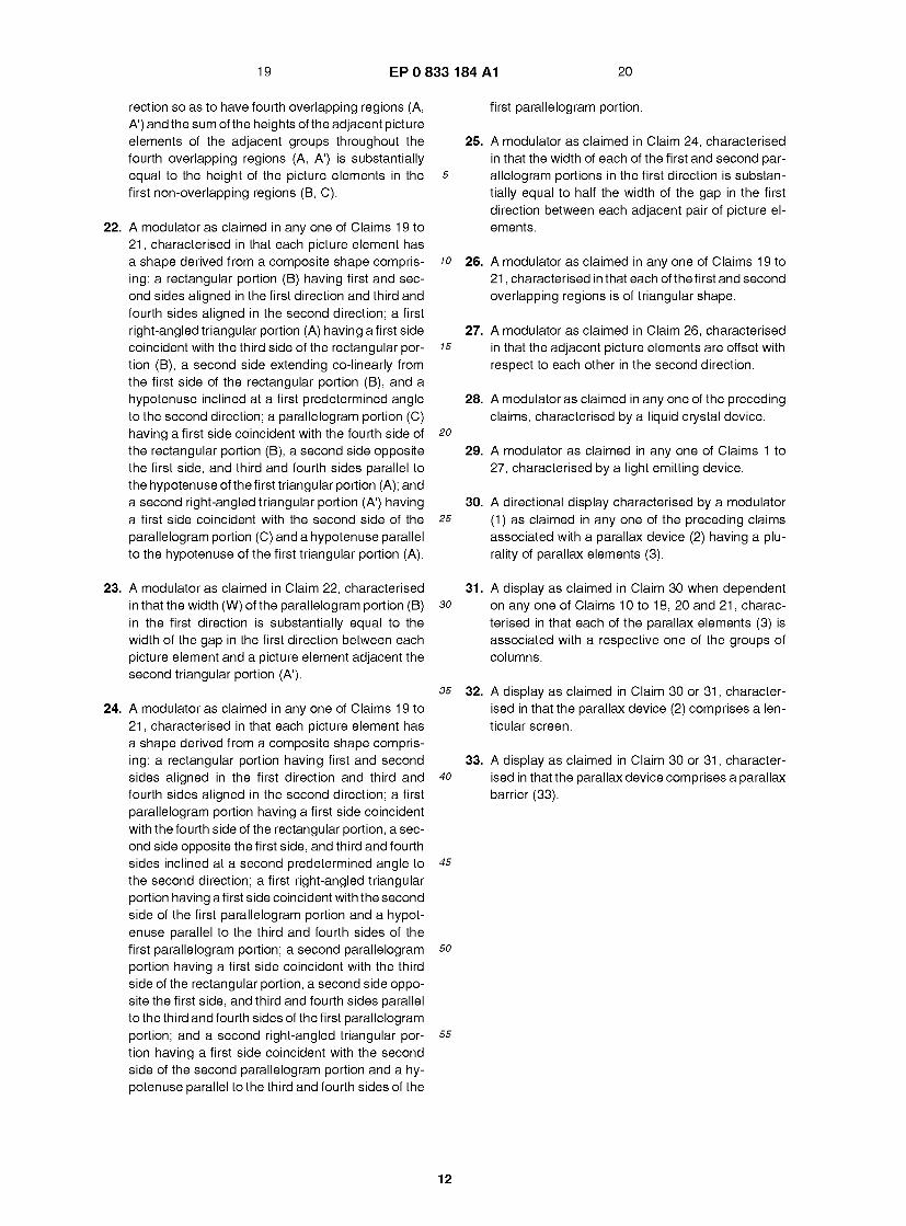
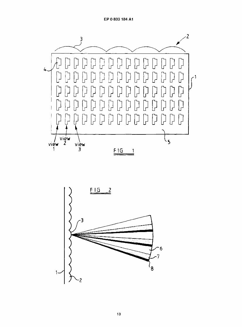
The autostereoscopic 3D display illustrated dia- grammatically in Figure 1 of the accompanying draw- ings comprises a known type of SLM 1 associated with a parallax device in the form of a lenticular screen 2. The SLM 1 has pixels arranged as horizontal rows and ver- tical columns. The display is of the type which provides three views in three adjacent viewing regions or win- dows for an observer. Thus, three columns of pixels are disposed behind each lenticule, such as 3, of the screen 2. The columns behind the lenticule 3 are indicated in Figure 1 as providing views 1, 2 and 3. The lenticule images the pixel columns into the three adjacent viewing windows.
The pixel columns display vertical slices of three two dimensional (2D) views taken in directions corre- sponding to the directions in which the three views are visible to an observer observing the 3D display. Thus, when the eyes of an observer are located in adjacent viewing windows, the observer sees a 3D image auto- stereoscopically i.e. without requiring any viewing aids.
The pixels such as 4 have the shape of two adjacent rectangles as defined by a black mask 5 of the SLM 1 . Further, the pixel columns are separated from each oth- er by vertical black mask strips. This gives rise to vari- ations in illumination intensity illustrated in Figure 2 of the accompanying drawings which is a diagrammatic plan view showing the SLM 1 and the lenticular screen 2. Each lenticule images the three associated columns of pixels 4 into viewing directions of varying illumination. For instance, the column containing the pixel 4 shown in Figure 1 gives rise to a region 6 of maximum illumi- nation corresponding to the portion of the pixel of great- est height, a region 7 of reduced illumination corre- sponding to the portion of the pixel of reduced vertical height, and a dark region 8 in which the vertical black mask strip between adjacent columns of pixels is im- aged by the lenticule 3. Thus, as an observer moves with respect to the display, the image intensity varies substantially and gives rise to undesirable visual arte- facts. Longitudinal and lateral viewing freedom is thus adversely Affected.
Irregular illumination as illustrated in Figure 2 is caused by differing vertical extents within the pixel shape. When light transmitted through the pixels is im- aged through the cylindrical lenses formed by the lenti- cules of the lenticular screen, there is no restriction on the vertical spreading of light. Thus, at a viewing window
3
3 EP0 833 184 A1 4
plane, a vertical strip of illumination is produced by each part of the pixel. The intensity of the illumination is di- rectly proportional to the vertical extent of the pixel. Thus, for constant illumination, a rectangular pixel shape is desirable. Also, in order to avoid dark regions between illuminated regions, the columns of pixels should be horizontally contiguous, at least below each lenticule.
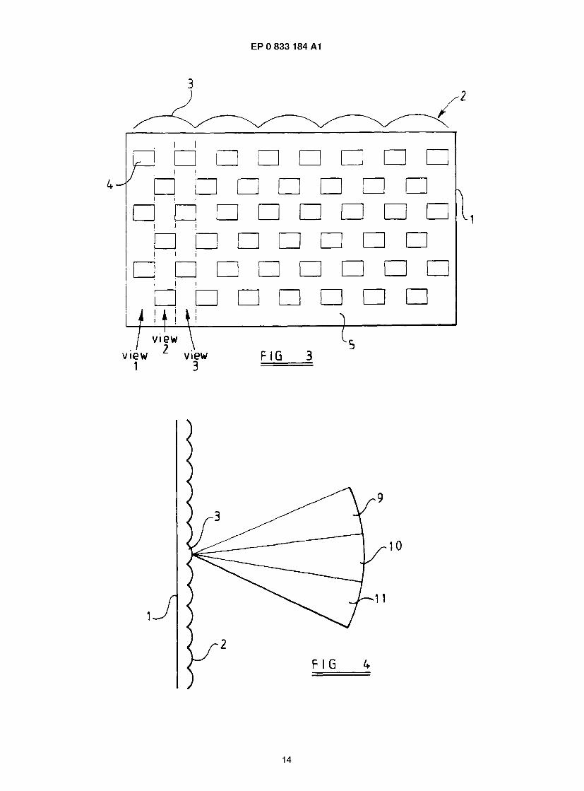
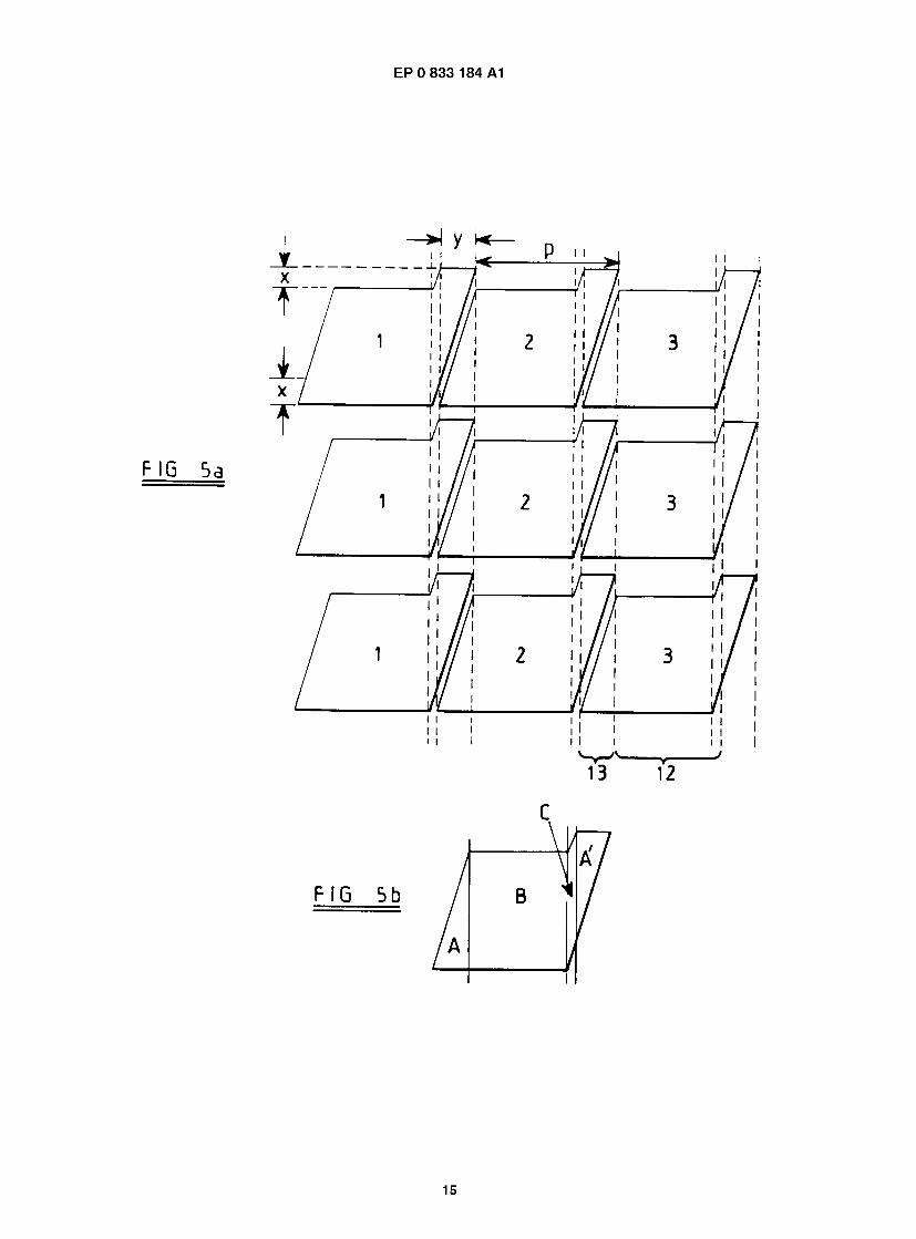
Figure 3 of the accompanying drawings illustrates an SLM of the type disclosed in EP 0 625 861 . The pixels are arranged as rows and columns such that the pixels in each column are horizontally contiguous with the pix- els of the or each adjacent column. Further, the pixels are of rectangular shape so as to have constant vertical extent across the width of the pixel. As shown in Figure 4 of the accompanying drawings, a display using this pixel arrangement provides contiguous viewing regions 9, 1 0 and 1 1 whose illumination intensity is substantially constant and unaffected by lateral movement of an ob- server.
In order to interleave the pixels of adjacent rows of the layout shown in Figure 3, the gaps between pixels must be at least as large as the pixels themselves. Thus, the maximum theoretical aperture ratio of an SLM 1 of the type shown in Figure 3 is 50%. However, in practice, space must be left between the pixels for the routing of electrical connections so that the maximum aperture ra- tio in practice is less than 50%.
Space must be allowed between the pixel apertures for the routing of conductors controlling the pixels. Such conductors generally comprise row conductors (normal- ly referred to as "gate lines" in standard thin film transis- tor LCDs), which extend essentially horizontally and connect all the pixels in each row, and column conduc- tors (referred to as "source lines") which extend essen- tially vertically and interconnect the pixels in each col- umn. In matrix addressed devices, the gate and source lines are addressed in sequence to control the pixels so as to avoid having an individual electrode connection for each pixel.
According to a first aspect of the invention, there is provided a spatial light modulator comprising a plurality of light output apertures arranged as rows extending in a first direction and columns extending in a second di- rection substantially perpendicular to the first direction, characterised in that at least one first one and at least one second one of the apertures overlap in the first di- rection so as to have first and second overlapping re- gions, respectively, such that the height in the second direction of each of the first and second overlapping re- gions varies and the sum of the heights of the first and second overlapping regions is substantially constant.
At least one of the first and second apertures may have a first non-overlapping portion whose height is substantially constant and is substantially equal to the sum of the heights of the first and second overlapping regions.
Each of the first and second overlapping regions
may be of right-angled triangular shape. The or each first and second apertures may be off-
set with respect to each other in the second direction. The or each first and second apertures may be sep-
5 arated by a gap containing an addressing electrode. The modulator may comprise a plurality of picture
elements, each of which comprises a first sub-picture element defined by one of the first apertures and a sec- ond sub-picture element defined by one of the second
10 apertures. The gaps may be inclined with respect to the second direction in opposite directions in adjacent rows of the picture elements.
The modulator may comprise an addressing tran- sistor for addressing the first and second sub-elements
is of each picture element. The modulator may comprise first and second ad-
dressing transistors for addressing the first and second sub-elements, respectively, of each picture element.
The picture elements may be arranged as groups 20 of N adjacent columns, where N is integer greater than
1, and adjacent picture elements disposed in each row and in adjacent columns of each group may overlap in the first direction so as to have third overlapping regions and second non-overlapping regions, the height of each
25 picture element being substantially constant throughout the second non-overlapping region and being substan- tially equal to the sum of the heights of the adjacent pic- ture elements throughout the third overlapping regions.
Adjacent picture elements disposed in each row 30 and in adjacent columns of adjacent groups may overlap
in the first direction so as have fourth overlapping re- gions and the sum of the heights of the adjacent picture elements of the adjacent groups throughout the fourth overlapping regions may be substantially equal to the
35 height of the picture elements in the second non-over- lapping regions.
Each picture element may have a shape derived from a composite shape comprising: a rectangular por- tion having first and second sides aligned in the first di-
40 rection and third and fourth sides aligned in the second direction; a first right-angled triangular portion having a first side coincident with the third side of the rectangular portion, a second side extending co-linearly from the first side of the rectangular portion, and a hypotenuse
45 inclined at a first pre-determined angle to the second direction; a parallelogram portion having a first side co- incident with the fourth side of the rectangular portion, a second side opposite the first side, and third and fourth sides parallel to the hypotenuse of the first triangular
so portion; and a second right-angled triangular portion having a first side coincident with the second side of the parallelogram portion and a hypotenuse parallel to the hypotenuse of the first triangular portion. The width of the parallelogram portion in the first direction may be
55 substantially equal to the width of the gap in the first di- rection between each picture element and a picture el- ement adjacent the second triangular portion.
Each picture element may have a shape derived
4
5 EP0 833 184 A1 6
from a composite shape comprising: a rectangular por- tion having first and second sides aligned in the first di- rection and third and fourth sides aligned in the second direction; a first parallelogram portion having a first side coincident with the fourth side of the rectangular portion, a second side opposite the first side, and third and fourth sides inclined at a second pre-determined angle to the second direction; a first right-angled triangular portion having a first side coincident with the second side of the first parallelogram portion and a hypotenuse parallel to the third and fourth sides of the first parallelogram por- tion; a second parallelogram portion having a first side coincident with the third side of the rectangular portion, a second side opposite the first side, and third and fourth sides parallel to the third and fourth sides of the first par- allelogram portion; and a second right-angled triangular portion having a first side coincident with the second side of the second parallelogram and a hypotenuse par- allel to the third and fourth sides of the first parallelogram portion. The width of each of the first and second paral- lelogram portions in the first direction may be substan- tially equal to half the width of the gap in the first direction between each adjacent pair of picture elements.
The shape may be derived by dividing the compos- ite shape obliquely with respect to the second direction so as to define the first and second apertures.
Each of the third overlapping regions may be of tri- angular shape, the adjacent picture elements may be offset with respect to each other in the second direction.
The apertures may define respective picture ele- ments. The picture elements may be arranged as groups of N adjacent columns, where N is an integer greater than 1 , and adjacent picture elements disposed in each row and in adjacent columns of each group may be defined by the first and second apertures. Adjacent picture elements disposed in each row and in adjacent columns of adjacent groups may overlap in the first di- rection so as to have fourth overlapping regions and the sum of the heights of the adjacent picture elements of the adjacent groups throughout the fourth overlapping regions may be substantially equal to the height of the picture elements in the first non-overlapping regions.
Each picture element may have a shape derived from a composite shape comprising: a rectangular por- tion having first and second sides aligned in the first di- rection and third and fourth sides aligned in the second direction; a first right-angled triangular portion having a first side coincident with the third side of the rectangular portion, a second side extending co-linearly from the first side of the rectangular portion and a hypotenuse inclined at a first pre-determined angle to the second direction; a parallelogram portion having a first side co- incident with the fourth side of the rectangular portion, a second side opposite the first side, and third and fourth sides parallel to the hypotenuse of the first triangular portion; and a second right-angled triangular portion having a first side coincident with the second side of the parallelogram portion and a hypotenuse parallel to the
hypotenuse of the first triangular portion. The width of the parallelogram portion in the first direction may be substantially equal to the width of the gap in the first di- rection between each picture element and a picture el-
5 ement adjacent the second triangular portion. Each picture element may have a shape derived
from a composite shape comprising: a rectangular por- tion having first and second sides aligned in the first di- rection and third and fourth sides aligned in the second
10 direction; a first parallelogram portion having a first side coincident with the fourth side of the rectangular portion, a second side opposite the first side, and third and fourth sides inclined at a second pre-determined angle to the second direction; a first right-angled triangular portion
is having a first side coincident with the second side of the first parallelogram portion and a hypotenuse parallel to the third and fourth sides of the first parallelogram por- tion; a second parallelogram portion having a first side coincident with the third side of the rectangular portion,
20 a second side opposite the first side, and third and fourth sides parallel to the third and fourth sides of the first par- allelogram portion; and a second right-angled triangular portion having a first side coincident with the second side of the second parallelogram portion and a hypote-
25 nuse parallel to the third and fourth sides of the first par- allelogram portion. The width of each of the first and sec- ond parallelogram portions in the first direction may be substantially equal to half the width of the gap in the first direction between each adjacent pair of pixels.
30 Each of the first and second overlapping regions may be of triangular shape. The adjacent picture ele- ments may be offset with respect to each other in the second direction.
The modulator may comprise a liquid crystal device. 35 The modulator may comprise a light emitting de-
vice. According to a second aspect of the invention, there
is provided a directional display characterised by a mod- ulator in accordance with the first aspect of the invention
40 associated with a parallax device having a plurality of parallax elements.
Each of the parallax elements may be associated with a respective one of the groups of columns.
The parallax device may comprise a lenticular 45 screen.
The parallax device may comprise a parallax barri- er.
It is thus possible to provide an SLM which is suit- able for use in directional displays and which has a rel-
50 atively high aperture ratio. For instance, where a display is provided by such an SLM and a backlight for illumi- nating the SLM, a backlight with lower power consump- tion may be used or a brighter display may be achieved. This is particularly advantageous where the SLM is used
55 in conjunction with a parallax barrier because the paral- lax barrier operates by restricting the light throughput so that an SLM of higher aperture ratio allows higher bright- ness to be achieved.
5
7 EP0 833 184 A1 8
Another advantage is that manufacturing toleranc- es of such an SLM may be relaxed. During manufacture of a typical SLM, a black mask is formed to define the pixel apertures. In the case of an SLM of the type dis- closed in EP 0 625 861 , manufacturing tolerances lead- s ing to horizontal deviations of the pixel apertures can result in a double brightness viewing region where the pixels overlap or a black viewing region where the pixels underlap. With the pixel arrangement disclosed herein, such manufacturing tolerances lead to an area of in- 10 creased or decreased intensity so that undesirable vis- ual artefacts are substantially reduced or eliminated.
It is further possible to allow opaque conductors to pass through the pixel apertures without visual arte- facts. This in turn allows high aperture ratios to be 15 achieved.
The present arrangement is advantageous for un- packed autostereoscopic 3D displays which generate a large number of views but which do not provide observer tracking. In such displays, the SLM resolution is of great 20 importance because the SLM must have N times the re- quired resolution per view, where N is the number of dis- played views. The relatively close packing of pixels is advantageous for high resolution, for improving the number of displayed views which is possible, and for im- 25 proving brightness. In such multiple view displays, sub- stantially contiguous viewing windows are important so as to maintain the transition between views as artefact- free as possible. If the viewing windows are not substan- tially contiguous, then black bars may be seen moving 30 across the display as the view changes.
The pixel arrangement disclosed herein is also ad- vantageous for observer tracking autostereoscopic 3D displays. Increased brightness may be provided togeth- er with electronic lateral and longitudinal tracking with- 35 out moving parts, for instance as disclosed in EP 0 726 482 and EP 0 721 131. However, mechanical observer tracking may also be used and benefits from the rela- tively wide uniform intensity windows which can be pro- duced. 40
Displays of the type disclosed herein may be used, for example, in office environment displays, 3D displays for lap top and personal computers, personal entertain- ment systems including computer games, 3D television, medical imaging, virtual reality, video phones and ar- 45 cade video games.
The invention will be further described, by way of example, with reference to the accompanying drawings, in which:
50 Figure 1 illustrates diagrammatically the pixel layout of a known type of LCD disposed behind a lenticular screen to form an autostereoscopic 3D display;
Figure 2 illustrates illumination regions produced by 55 the display of Figure 1 ;
Figure 3 illustrates a display comprising another
known type of SLM;
Figure 4 illustrates illumination regions produced by the display of Figure 3;
Figures 5a and b illustrate a novel pixel arrange- ment of an StM constituting an embodiment of the invention;
Figure 6 illustrates illumination regions produced by an autostereoscopic 3D display using the layout il- lustrated in Figure 5;
Figure 7 illustrates some important dimensions of the pixel arrangement illustrated in Figure 5;
Figures 8a and b illustrate the effects of positional errors for a known type of pixel arrangement and for the arrangement illustrated in Figure 5, respec- tively;
Figure 9 illustrates the origin of an "eye spot" in an autostereoscopic 3D display;
Figure 10 illustrates another pixel arrangement of an SLM constituting an embodiment of the inven- tion;
Figure 11 illustrates another pixel arrangement of an SLM constituting an embodiment of the inven- tion;
Figure 1 2 illustrates an autostereoscopic 3D display using the pixel layout illustrated in Figure 11;
Figure 13 illustrates another 3D autostereoscopic display constituting an embodiment of the invention and having another pixel arrangement;
Figure 14 illustrates an alternative colour filter ar- rangement for the display of Figure 1 3;
Figures 1 5a, b and c show 3D autostereoscopic dis- plays constituting embodiments of the invention for providing mechanical observer tracking;
Figure 16 shows a display constituting an embodi- ment of the invention for providing observer tracking by rotation of the whole display;
Figure 17 illustrates a pixel arrangement for use in a mechanical observer tracking display;
Figure 1 8 illustrates another pixel layout for an SLM constituting an embodiment of the invention;
Figure 1 9 illustrates the layout of Figure 1 8 showing a possible arrangement of addressing electrodes;
6
9 EP0 833 184 A1 10
Figure 20 illustrates a pixel layout of the type shown in Figures 1 8 and 1 9 but modified to provide an im- proved addressing electrode layout;
Figure 21 illustrates a pixel driving arrangement us- ing two thin film transistors per pixel;
Figure 22 illustrates a pixel drive arrangement using a single thin film transistor per pixel; and
Figure 23 illustrates another pixel arrangement of an SLM constituting an embodiment of the inven- tion.
Like reference numerals refer to like parts through- out the drawings.
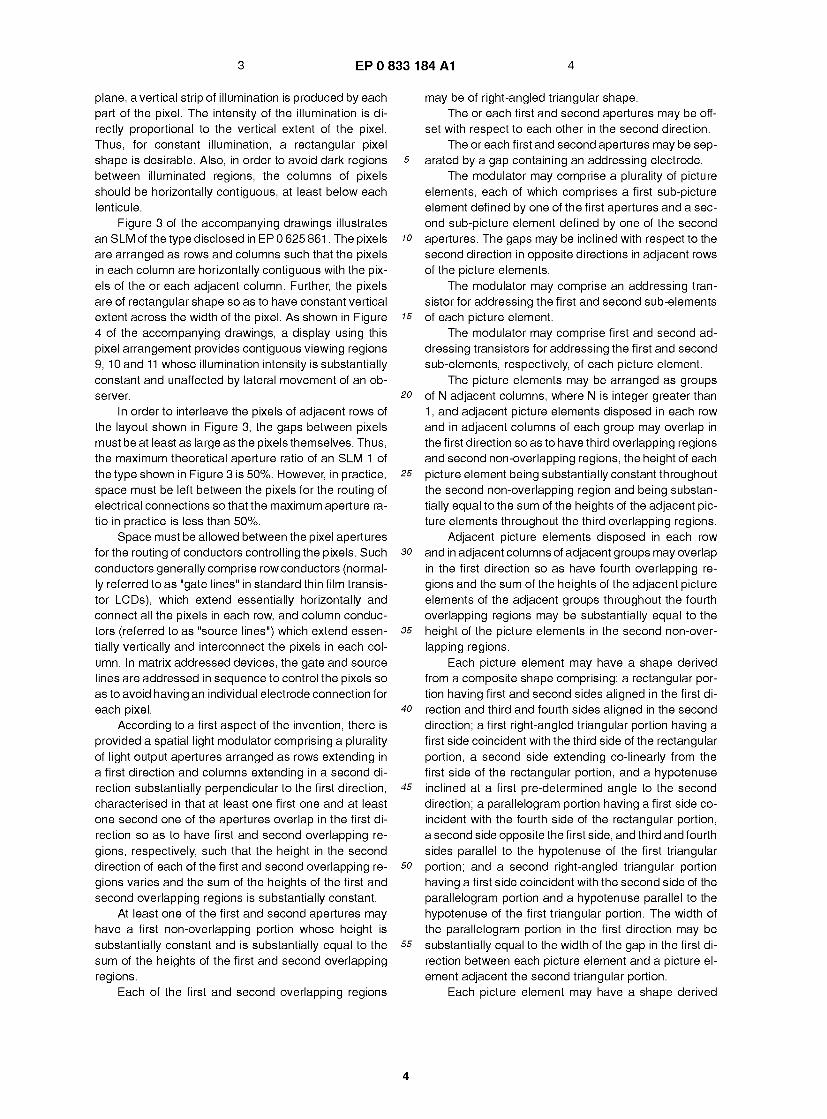
Figures 5a and b illustrate a pixel arrangement for an SLM constituting an embodiment of the invention. The arrangement provides closer packing of the pixels such that the pixels can be disposed in the same hori- zontal row without the vertical offset required in arrange- ments of the type shown in Figure 3. Nevertheless, hor- izontal and vertical gaps between the pixels are provid- ed for routing of the gate and source lines.
The shape of each pixel comprises four regions la- belled A, B, C and A'. The region A at the left of each pixel is shaped as a right angled triangle whose hypot- enuse is inclined at an angle to the vertical which match- es the inclination or slope of the right-hand edge of the pixel immediately to its left. The region B is rectangular so as to have a constant vertical extent and this is con- nected to the region C of parallelogram shape. Finally, another right angled triangular section is provided at A'.
The pixels are disposed such that there is a region 12 where there is no horizontal overlap between adja- cent pixels and a region 1 3 where adjacent pixels over- lap horizontally. In the region 13, the portion A of the right-hand pixel overlaps with the region A' of the left- hand pixel. Because the sloping edges of the regions A and A' match each other, the sum of the vertical extents of the adjacent pixels throughout the overlapping region 1 3 is constant and equal to the vertical extent of the rec- tangular region B. The transition between the region B and the region A' comprises the parallelogram-shaped region C, which is also of constant vertical extent.
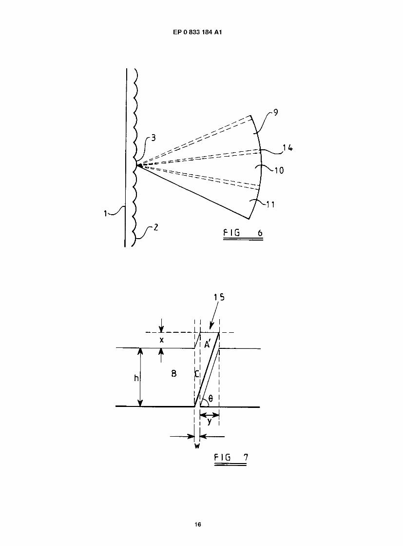
Figure 6 illustrates the illumination produced by an autostereoscopic 3D display using the pixel arrange- ment shown in Figure 5. Three adjacent viewing regions 9, 10 and 11 are produced but with overlap regions be- tween adjacent pairs, for instance as shown at 14, cor- responding to imaging by the lenticule 3 of the overlap- ping region 13. Thus, the display provides continuous and substantially uniform illumination with thin overlap regions, potentially containing high levels of cross talk, over which substantially constant illumination is main- tained. The requirement that adjacent columns of pixels show the same view information so as to keep the illu- mination constant when an observer eye crosses the
boundary between windows may, for instance, be met by the lateral observer tracking arrangement disclosed in EP 0 726 482.
The overlap region reduces viewing freedom in 5 front of the display when adjacent columns of pixels do
not show the same view information. The loss in viewing freedom is related to the size of the overlap shown at y in Figure 5(a) in relation to the total pixel size shown at p in Figure 5(a). In order to minimise the loss of viewing
10 freedom, y should be much less than p. Figure 7 illustrates various dimensions of the pixel
arrangement shown in Figure 5a. The height of the rec- tangular portion B is indicated by h whereas the height or projection above the portion B of a "tab" portion indi-
15 cated at 15 is designated x. The sides of the pixel are inclined at a slope angle 6. The horizontal gap between adjacent pixels is designated w. These parameters are related by the following expressions:
20 x = wtan(6)
y tan(9) 25
In order to give a good packing density and thus a high aperture ratio, the parameter x should be as small as possible. In order to maximise viewing freedom, y should be as small as possible. The slope angle 6 is thus
30 chosen to provide an acceptable compromise between these two conflicting requirements.
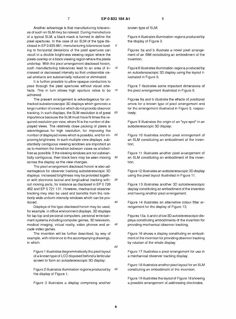
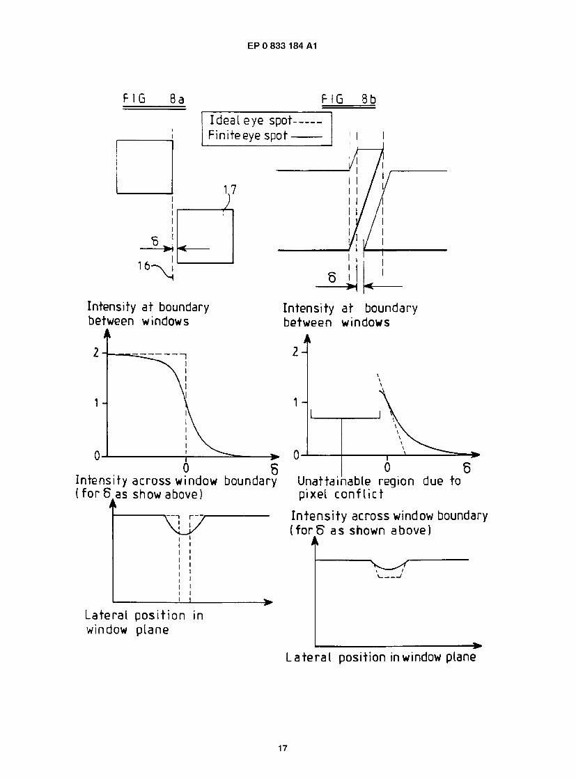
Figures 8a and b illustrate the effects on intensity at the boundary between two windows of manufacturing tolerances in positioning of the pixels. Figure 8a illus-
35 trates this effect for a known pixel arrangement of the type shown in Figure 3. The broken line 16 in the upper part of Figure 8a illustrates the desired position for the left edge of the pixel 17 and the manufacturing error or tolerance resulting in an underlap is indicated by 8.
40 The graph at the middle part of Figure 8a illustrates how the intensity varies at the boundary between the windows as the tolerance 8 varies either side of zero corresponding to perfect positioning in terms of intensity where "1" is the desired constant intensity. Thus, if the
45 pixels are slightly misplaced during manufacture of the SLM, the viewing window boundary will either have dou- ble the intensity or zero intensity depending on whether the tolerance is such as to create an overlap or an un- derlap. However, the size of the eye spot blurs this
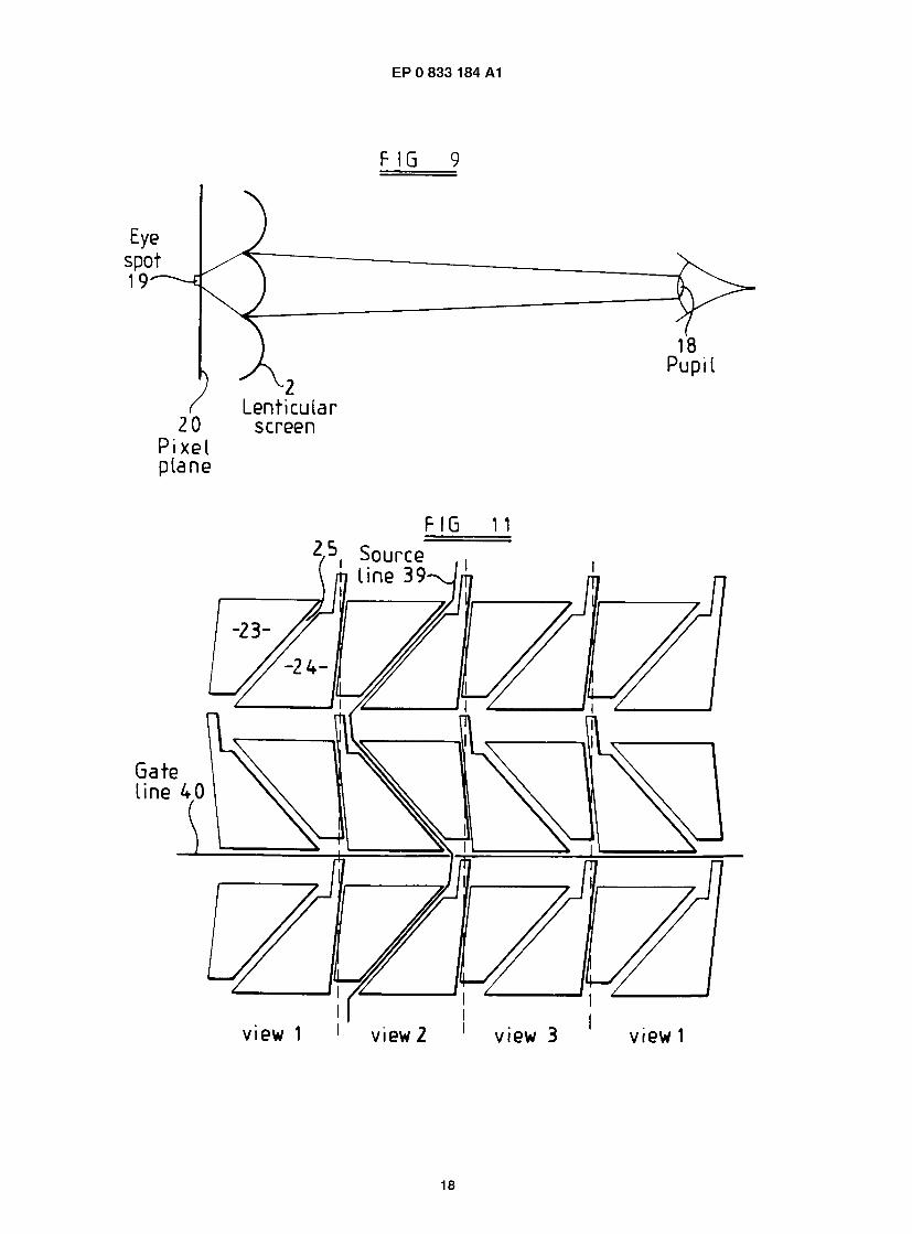
50 somewhat. Figure 9 illustrates how the lenticular screen 2 of
the display images the pupil 1 8 to an eye spot 1 9 of finite size at the pixel plane 20 of the SLM. For cylindrically converging lenticular screens 2, the pupil is in fact im-
55 aged to a vertical strip and this eye spot 1 9 covers the region of the SLM from which the pupil of the observer eye collects light. Thus, the incorrect pixel positioning is perceived as a rise or fall in intensity with the magnitude
20
7
11 EP0 833 184 A1 12
thereof given by the relative sizes of the eye spot and the degree of mismatch. However, the eye is very sen- sitive to small intensity changes, especially when the ob- server is not at the ideal window plane. Intensity fluctu- ations less than 1% are visible so that the required tol- erance of positioning the pixels for the arrangement shown in Figure 3 is very high and is typically of the order of 0.1 micrometres.
The graph at the middle part of Figure 8a shows the variation of intensity with horizontal pixel positioning tol- erance for an ideal "point" eye spot by means of the bro- ken line curve. The actual variation for an eye spot of finite size is illustrated by the unbroken line curve. The graph at the lower part of Figure 8a illustrates the vari- ation in intensity as an observer moves laterally in the window plane with the broken and unbroken curves rep- resenting intensity for ideal and finite eye spots, respec- tively.
Figure 8b illustrates the effect of mismatch for the pixel arrangement shown in Figure 5a. In this case, for the ideal eye spot, the viewing window boundary inten- sity drops linearly as the mismatch approaches the over- lap size. For the actual finite eye spot, the rate of fall is slower so that the tolerance in positioning the pixels may be relaxed. For instance, considering a specific numer- ical example, if the eye spot is approximately 1 0 microns in diameter, the overlap width is 3 microns, and the limit of illumination drop which can be tolerated is 1%, then a mismatch of about 15% of the overlap width can be allowed and represents about 0.5 microns in this exam- ple. Again, the lower part of Figure 8b illustrates the var- iation of intensity with lateral position of the observer for the same underlap shown in the upper parts of Figures 8a and 8b. The intensity variation is substantially re- duced as compared with the lower part of Figure 8a. Thus, the arrangement shown in Figure 5a permits man- ufacturing tolerances which are greater than those per- mitted in the arrangement of Figure 3 for similar perform- ance.
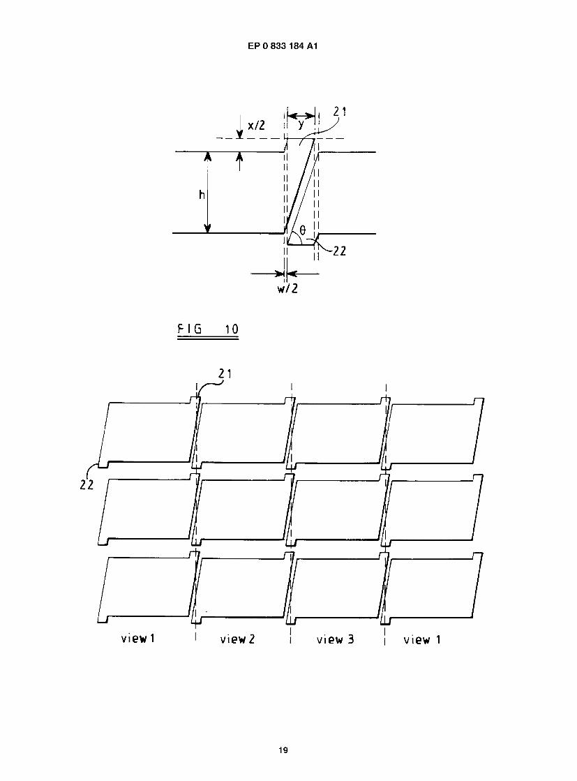
Figure 10 illustrates a pixel arrangement which dif- fers from that shown in Figure 5a in that the tab 1 5 pro- vided at one end of each pixel is replaced by two tabs 21 and 22 at opposite ends of each pixel. Thus, the tab region is shared between adjacent pixels in the overlap region and, if this is done equally, the tab height be- comes x/2 i.e. half the tab height shown in Figure 7. The performance of this arrangement is the same as that of the arrangement shown in Figure 5a.
Where the SLM is embodied as an LCD display with a diagonal size of 8 to 1 0 inches, the pixels typically have a width and height of approximately 100 micrometres. Separations between pixels vary significantly with dif- ferent display technologies but a conductor width of 10 to 20 micrometres is possible in more recent displays. If this is taken as the required horizontal gap w, then the overlap region would be undesirably large. However, Figure 1 1 illustrates an arrangement which may be used to overcome this difficulty.
In Figure 1 1 , each pixel is divided into two subpixels such as 23 and 24 by a diagonal dividing line and the subpixels are offset vertically with respect to each other so as to form a gap 25 which can be made sufficiently
5 large to accommodate the conductor electrode such as a vertical electrode or "source line" 39. The slopes of the opposing edges of the subpixels are the same and, because there is no horizontal offset between subpixels, the vertical aperture size is maintained constant across
10 the centre of the pixel. Thus, the gap 25 in the pixel is effectively invisible and causes no undesirable visual ar- tefacts in 3D displays using cylindrical components. Routing of a horizontal electrode or "gate line" is shown at 40. The vertical space taken up by dividing the pixel
is into subpixels can be small because the slope of the di- viding line may be relatively shallow, for instance 45°, as viewing freedom is not compromised.
With the electrodes routed in this way, the pixels may be moved much closer together so that the gap w
20 can be significantly reduced, remaining only to insulate the pixel pad electrodes from each other and to avoid fringing field effects in the LCD between horizontally ad- jacent pixels. As shown in Figure 11, the slopes of the diagonal gaps such as 25 are reversed in alternate rows
25 so as to provide shorter connection paths for the vertical conductor lines.
In order to permit observer tracking without moving parts for instance as disclosed in EP 0 726 482, the con- dition y<p/2 should be met. This condition is derived
30 from how close an eye may approach a pixel boundary while the other eye is moving between two pixels in a three window tracking system. The condition y<p/8 is probably desirable for a high quality practical system.
In the case of a typical example, h = p =100 mi- 35 crometres, the width of the conductor lines is 15 mi-
crometres and the remaining gap w between pixels is 3 micrometres. A slope angle 6 of approximately 85° gives an overlap region whose width y is 9 micrometres and a tab height x of 34 micrometres. Using the arrangement
40 shown in Figure 1 1 , the slope angle of the dividing line between subpixels is approximately 53° giving a vertical offset of 25 micrometres between the subpixels 23 and 24. With a vertical gap between adjacent pixels of 15 micrometres for the gate lines, this provides an aperture
45 ratio of 67% for the arrangement shown in Figure 11 compared with 43.5% for the arrangement shown in Fig- ure 3. The arrangement shown in Figure 11 thus pro- vides a 54% improvement in aperture ratio.
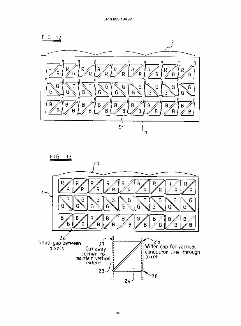
In order to provide a full colour display, red, green so and blue pixels must be arranged so that the pixel
groups for each view contain sufficient of each for cor- rect colour balance. Figure 12 illustrates the use of an SLM 1 with the pixel arrangement shown in Figure 1 1 in association with the lenticular screen 2 so as to provide
55 a three view autostereoscopic 3D display. The pixels of the top row are provided with a red filter, the pixels of the middle row are provided with a green filter and the pixels of the bottom row are provided with a blue filter.
8
13 EP0 833 184 A1 14
This pattern is repeated vertically and horizontally, Fig- ure 12 merely showing a small portion of the display.
In some applications, a small gap between viewing windows can be tolerated. For instance, this may be possible in 3D autostereoscopic displays provided with mechanical observer tracking which prevents the ob- server eye spots from crossing a pixel boundary by lat- erally displacing the parallax element, such as the len- ticular screen 2, to keep the eye spot in the pixel centre.
The presence of a small gap between adjacent win- dows manifests itself as a thin dark region which is im- aged to a dark strip down the centre of an observer's face. Such a region is not therefore visible and is unno- ticed by the observer. In order to keep the gap invisible, it must be as small as possible and the space required for a vertical conductor line might cause too wide a gap between the windows when imaged.
In order to overcome this problem, the arrangement shown in Figure 1 3 may be used. The SLM 1 comprises rows and columns of pixels which are spaced closer to- gether. However, the pixel columns are separated from each other by a small vertical gap shown at 26. Each pixel is divided into subpixels 23 and 24 so as to provide a wider gap 25 for accommodating the vertical conduc- tor line. In order to provide a pixel whose effective height is constant with lateral position, the corners 27 and 28 are "cut away" so as to maintain constant vertical extent.
Another example of a display which can cope with small gaps between pixel columns is a display using a parallax barrier as the parallax element or " view defin- ing optic". The eye spot is generally so large with a par- allax barrier that a small mismatch between the pixels is not noticeable to the observer if the mismatch is much less than this size. The SLM arrangement shown in Fig- ure 1 3 is therefore suitable for such a display. Because the gap between adjacent pixels has to be smaller than the width of a typical current conductor line, the conduc- tor lines pass through the gaps 25 between the subpix- els 23 and 24 of the pixels.
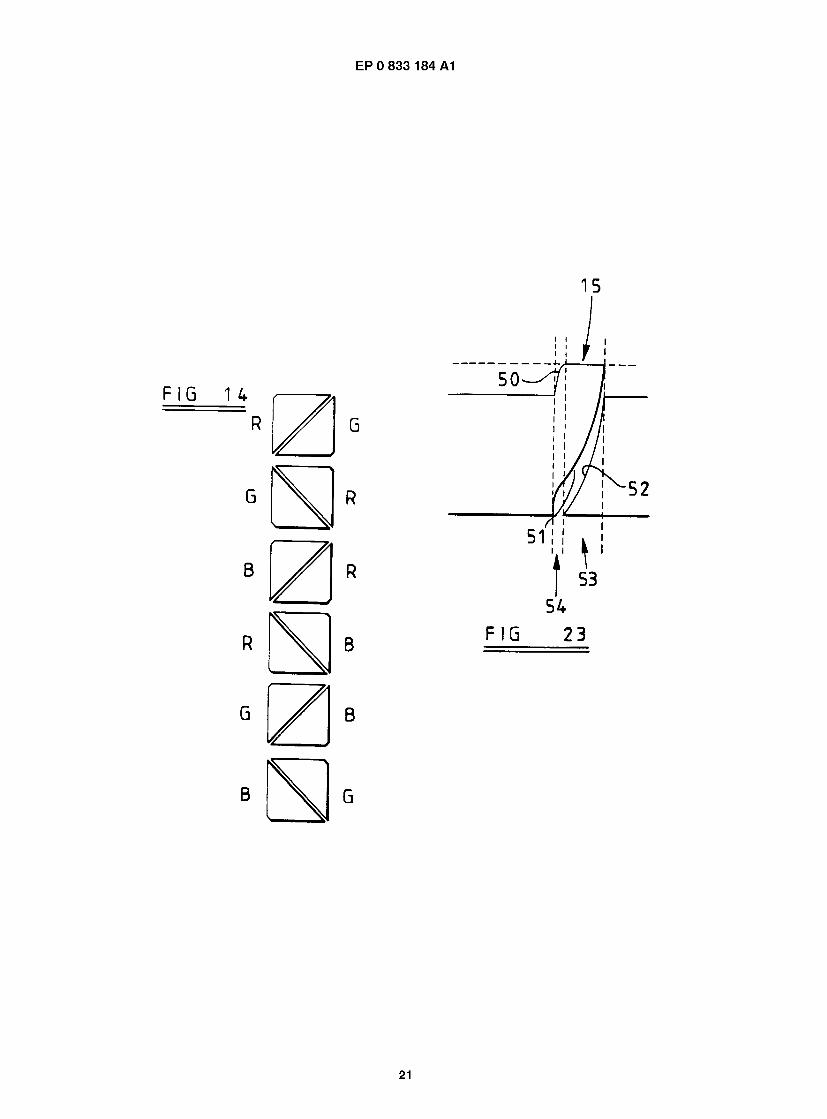
The arrangement shown in Figure 13 uses the same colour filter arrangement as described with reference to Figure 12. However, it is not necessary for both pixels to have the same colour filter, although corresponding colour halves should not be displaced far. Figure 14 il- lustrates an example of an arrangement in which the subpixels have different colour filters indicated by R for red, G for green and B for blue.
With the arrangement shown in Figure 1 3, it is pos- sible for all the conductors which are required to extend vertically to be accommodated in the gaps 25 between the subpixels 23 and 24. The gaps between adjacent pixels may therefore be minimised so as to provide an SLM 1 of very high aperture ratio with minimal horizontal gap between adjacent pixels.
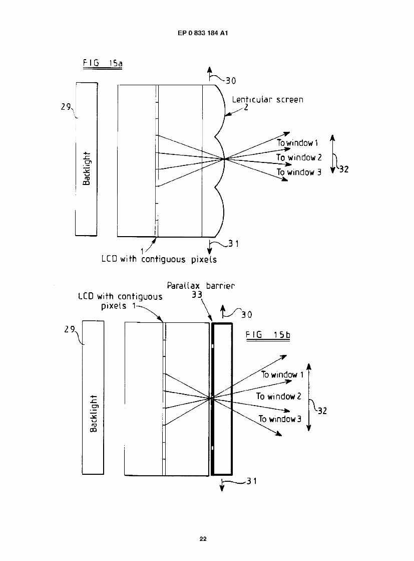
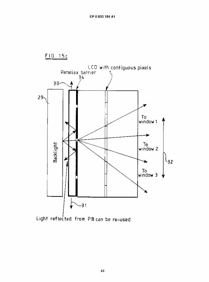
Figure 15a, b and c illustrate autostereoscopic 3D displays having mechanical observer tracking using SLMs of the type illustrated in Figure 13. The displays comprise a backlight 29 and a parallax device which is
moveable over the surface of the SLM 1 in response to a signal from a tracker device, such as a Dynasight (TM) infrared tracker. Such systems need only provide two viewing windows for displaying only a left image and a
5 right image because the observer is prevented from leaving the two windows by the dynamic tracking sys- tem. Figure 1 5a illustrates a display in which the parallax device is the lenticular screen 2 which is movable in the directions of arrows 30 and 31 so as to move the viewing
10 windows in the directions indicated by the arrow 32. The display of Figure 15b differs from that of Figure 15a in that the lenticular screen 2 is replaced by a front parallax barrier 33. The display shown in Figure 1 5c differs from that shown in Figure 1 5b in that the front parallax barrier
is 33 is replaced by a rear parallax barrier 34 disposed be- tween the backlight 29 and the LCD 1. In all three dis- plays, the SLM 1 comprises an LCD having pixels which are laterally contiguous so as to provide contiguous viewing windows.
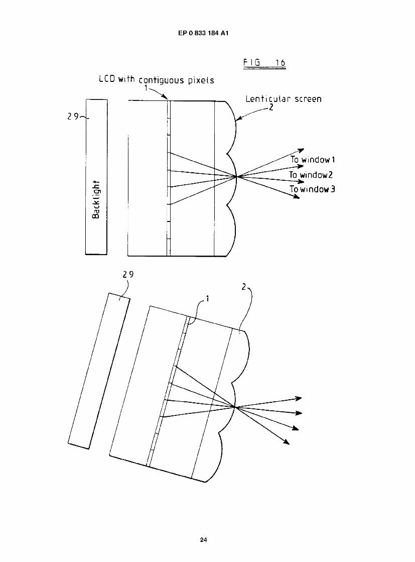
20 Figure 16 illustrates another observer tracking tech- nique for a display of the type shown in Figure 15a. In this case, the lenticular screen 2 is fixed and the whole display rotates in response to an observer position de- termining system.
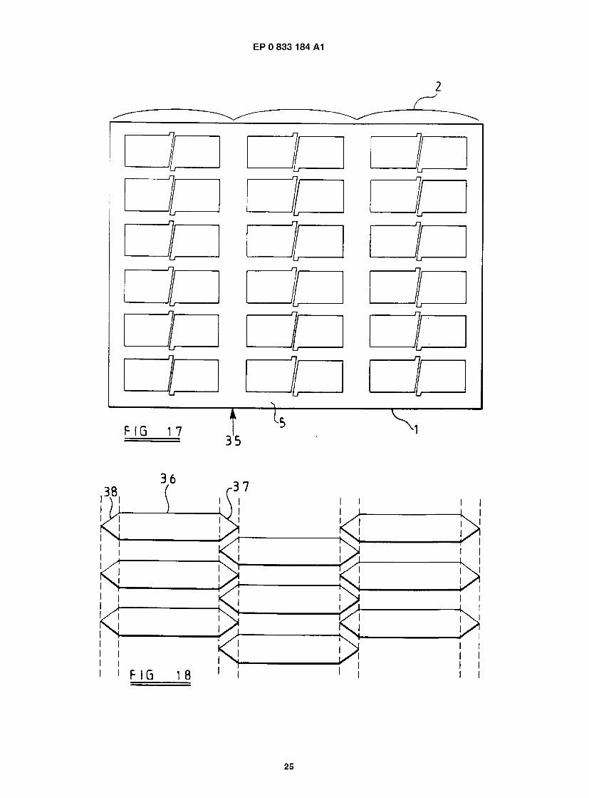
25 Figure 17 illustrates a display of the type shown in Figure 10 but with the pixels arranged as pairs of over- lapping columns below respective lenticules of the len- ticular screen 2. The pairs of columns are separated by continuous vertical black strips, such as 35, of the black
30 mask 5. This arrangement reduces cross-talk permea- tion while maintaining viewing freedom and maximising display resolution. Cross-talk occurs because of light leaking into a viewing window from neighbouring re- gions. By providing a dark space 35 between the pairs
35 of pixels, light leaks in from one side of the viewing win- dow only. Also, the black mask areas can be used for the routing of conductors. By using the pixel shapes with the tabs divided between the adjacent pixels, the pixel areas are maintained equal, which is desirable for
40 matched pixel capacitance in the display. Figure 18 illustrates another pixel arrangement for
an SLM. Each of the pixels is of hexagonal shape and comprises a rectangular central portion 36, which does not overlap with the adjacent pixels in the same row to-
45 gether with triangular end portions 37 and 38 which do overlap with the adjacent pixels in the same row. Adja- cent pairs of pixels in the same row are vertically offset with respect to each other. Again, in each row, there is a constant vertical extent or aperture across the whole
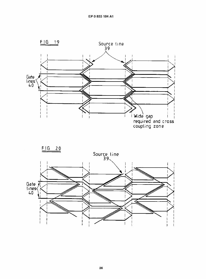
so row including the overlapping triangular regions. Figure 1 9 illustrates a possible arrangement of rout-
ing of source lines 39 and gate lines 40. Such an ar- rangement requires that, in certain gaps between adja- cent pixels, the gate and source lines will run parallel to
55 each other. Thus requires a relatively large gap and pos- sibly leads to an overlap region which is too large in com- parison with the central width of the windows. Further, because the conductors run alongside each other, some
9
15 EP0 833 184 A1 16
cross-coupling will take place between the signals car- CI ried by the conductors, thus leading to degradation in signal quality. 1.
Figure 20 illustrates an alternative arrangement in which the source lines 39 pass through the pixel aper- s tures in gaps created by dividing each pixel into subpix- els as described hereinbefore.
This arrangement is limited because the gate lines must pass through gaps between the pixels. When the width of the conductors, for instance 1 5 to 20 microme- 10 tres, is taken into account with a typical pixel pitch of approximately 1 00 micrometres, the overlap region can- not be made sufficiently small compared to the central part of the windows for good viewing freedom for ob- server tracking displays comprising LCD panels of 15 about 10 inches diagonal size. Thus, this arrangement is more appropriate for panels with large pixel pitches, 2. for instance large diagonal size SLMs.
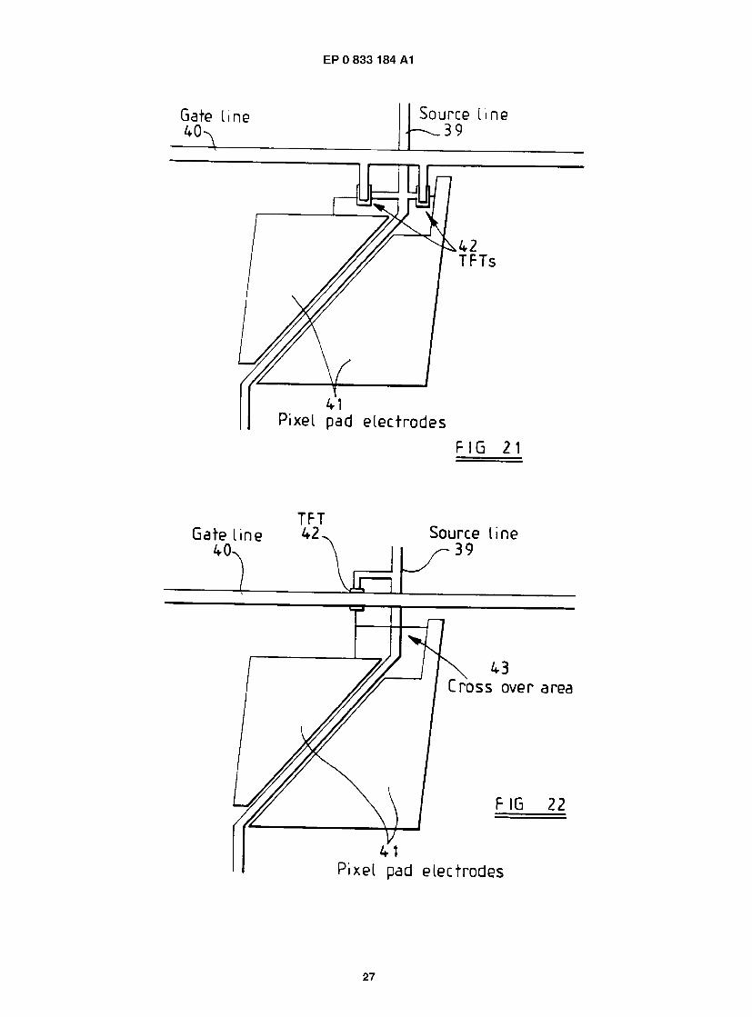
In thin film transistor type LCD displays, each pixel is driven by a thin film transistor fabricated on the display 20 substrate. The gate lines are connected to the transistor gates and the source lines are connected to the transis- tor sources. The pixel pad electrode is connected to the transistor drain. The positioning and number of thin film 3. transistors is importantforthefabrication of such display 25 panels and for cost. The display may also be embodied in other active matrix technology, such as thin film di- odes and metal-insulator-metal structures. 4.
Figure 21 illustrates a first arrangement for driving pixels which are divided into subpixels as shown in Fig- 30 ures 11 to 14 and 20. In this arrangement, the pixel pad electrodes 41 are driven by respective thin film transis- tors (TFTs) 42 so that there are two transistors per pixel. 5. However, for cost and manufacturing yield, it will be de- sirable to use a single thin film transistor per pixel as 35 shown in the arrangement of Figure 22. In this arrange- ment, one of the subpixel pad electrode connections crosses the vertical source line 39 and so has to be in- 6. sulated therefrom, for instance by a suitable dielectric layer. Although some capacitance will be generated in 40 the cross-over area 43, this may be made much less than the pixel capacitance so that the cross-over capac- itance is unimportant and the single transistor option is feasible.
Although the arrangements described hereinbefore 45 7. have included pixels having straight edges, particularly the inclined adjacent edges of horizontally adjacent pix- els, this is not necessary. For instance, Figure 23 illus- trates an arrangement which is similar to that shown in Figures 5a, 5b and 7 but which differs in that the edges so 50, 51 and 52 are curved. The curves are such that the 8. combined vertical extent of the pixels in the overlap re- gion 53 is constant and equal to the vertical extent or height in the non-overlapping region including the tran- sition region 54. 55
9.
A spatial light modulator (1) comprising a plurality of light output apertures arranged as rows extend- ing in a first direction and columns extending in a second direction substantially perpendicular to the first direction, characterised in that at least one first one and at least one second one of the apertures overlap in the first direction so as to have first and second overlapping regions (A, A'), respectively, such that the height in the second direction of each of the first and second overlapping regions (A, A') varies and the sum of the heights of the first and second overlapping regions (A, A') is substantially constant.
A modulator as claimed in Claim 1 , characterised in that at least one of the first and second apertures has a first non-overlapping portion (B, C) whose height is substantially constant and is substantially equal to the sum of the heights of the first and sec- ond overlapping regions (A, A').
A modulator as claimed in Claim 1 or 2, character- ised in that each of the first and second overlapping regions (A, A') is of right-angled triangular shape.
A modulator as claimed in any one of the preceding claims, characterised in that the or each first and second apertures are offset with respect to each other in the second direction.
A modulator as claimed in any one of the preceding claims, characterised in that the or each first and second apertures are separated by a gap contain- ing an addressing electrode (39).
A modulator as claimed in any one of the preceding claims, characterised by a plurality of picture ele- ments, each of which comprises a first sub-picture element (23) defined by one of the first apertures and a second sub-picture element (24) defined by one of the second apertures.
A modulator as claimed in Claim 6 when dependent on Claim 5, characterised in that the gaps (25) are inclined with respect to the second direction in op- posite directions in adjacent rows of the picture el- ements.
A modulator as claimed in Claim 6 or 7, character- ised by an addressing transistor (42) for addressing the first and second sub-elements (23, 24) of each picture element.
A modulator as claimed in Claim 6 or 7, character- ised by first and second addressing transistors (42) for addressing the first and second sub-elements
10
17 EP0 833 184 A1 18
(23, 24), respectively, of each picture element.
10. A modulator as claimed in any one of Claims 6 to 9, characterised in that the picture elements are ar- ranged as groups of N adjacent columns, where N is an integer greater than one, and adjacent picture elements disposed in each row and in adjacent col- umns of each group overlap in the first direction so as to have third overlapping regions (A, A') and sec- ond non-overlapping regions (B, C), the height of each picture element being substantially constant throughout the second non-overlapping region (B, C) and being substantially equal to the sum of the heights of the adjacent picture elements throughout the third overlapping regions (A, A').
11. A modulator as claimed in Claim 10, characterised in that adjacent picture elements disposed in each row and in adjacent columns of adjacent groups overlap in the first direction so as to have fourth overlapping regions (A, A') and the sum of the heights of the adjacent picture elements of the ad- jacent groups throughout the fourth overlapping re- gions (A, A') is substantially equal to the height of the picture elements in the second non-overlapping regions (B, C).
12. A modulator as claimed in Claim 10 or 11 , charac- terised in that each picture element has a shape de- rived from a composite shape comprising: a rectan- gular portion (B) having first and second sides aligned in the first direction and third and fourth sides aligned in the second direction; a first right- angled triangular portion (A) having a first side co- incident with the third side of the rectangular portion (B), a second side extending co-linearly from the first side of the rectangular portion (B), and a hypot- enuse inclined at a first predetermined angle to the second direction; a parallelogram portion (C) hav- ing a first side coincident with the fourth side of the rectangular portion (B), a second side opposite the first side, and third and fourth sides parallel to the hypotenuse of the first triangular portion (A); and a second right-angled triangular portion (A1) having a first side coincident with the second side of the par- allelogram portion (C) and a hypotenuse parallel to the hypotenuse of the first triangular portion (A).
13. A modulator as claimed in Claim 12, characterised in that the width (W) of the parallelogram portion (C) in the first direction is substantially equal to the width of the gap in the first direction between each picture element and a picture element adjacent the second triangular portion (A1).
14. A modulator as claimed in Claim 10 or 11 , charac- terised in that each picture element has a shape de- rived from a composite shape comprising: a rectan-
gular portion having first and second sides aligned in the first direction and third and fourth sides aligned in the second direction; a first parallelogram portion having a first side coincident with the fourth
5 side of the rectangular portion, a second side oppo- site the first side, and third and fourth sides inclined at a second predetermined angle to the second di- rection; a first right-angled triangular portion having a first side coincident with the second side of the
10 first parallelogram portion and a hypotenuse paral- lel to the third and fourth sides of the first parallelo- gram portion; a second parallelogram portion hav- ing a first side coincident with the third side of the rectangular portion, a second side opposite the first
is side, and third and fourth sides parallel to the third and fourth sides of the first parallelogram portion; and a second right-angled triangular portion having a first side coincident with the second side of the second parallelogram portion and a hypotenuse
20 parallel to the third and fourth sides of the first par- allelogram portion.
15. A modulator as claimed in Claim 14, characterised in that the width of each of the first and second par-
25 allelogram portions in the first direction is substan- tially equal to half the width of the gap in the first direction between each adjacent pair of picture el- ements.
30 16. A modulator as claimed in any one of Claims 12 to 1 5, characterised in that the shape is derived by di- viding the composite shape obliquely with respect to the second direction so as to define the first and second apertures.
35 17. A modulator as claimed in Claim 10 or 11 , charac-
terised in that each of the third overlapping regions is of triangular shape.
40 18. A modulator as claimed in Claim 17, characterised in that the adjacent picture elements are offset with respect to each other in the second direction.
19. A modulator as claimed in any one of Claims 1 to- 45 5, characterised in that the apertures define respec-
tive picture elements.
20. A modulator as claimed in Claim 19, characterised in that the picture elements are arranged as groups
so of N adjacent columns, where N is an integer great- er than one, and adjacent picture elements dis- posed in each row and in adjacent columns of each group are defined by the first and second apertures.
55 21. A modulator as claimed in Claim 20 when depend- ent on Claim 2, characterised in that adjacent pic- ture elements disposed in each row and in adjacent columns of adjacent groups overlap in the first di-
15
11
19 EP0 833 184 A1 20
rection so as to have fourth overlapping regions (A, A') and the sum of the heights of the adjacent picture elements of the adjacent groups throughout the fourth overlapping regions (A, A') is substantially equal to the height of the picture elements in the first non-overlapping regions (B, C).
22. A modulator as claimed in any one of Claims 1 9 to 21, characterised in that each picture element has a shape derived from a composite shape compris- ing: a rectangular portion (B) having first and sec- ond sides aligned in the first direction and third and fourth sides aligned in the second direction; a first right-angled triangular portion (A) having a first side coincident with the third side of the rectangular por- tion (B), a second side extending co-linearly from the first side of the rectangular portion (B), and a hypotenuse inclined at a first predetermined angle to the second direction; a parallelogram portion (C) having a first side coincident with the fourth side of the rectangular portion (B), a second side opposite the first side, and third and fourth sides parallel to the hypotenuse of the first triangular portion (A); and a second right-angled triangular portion (A1) having a first side coincident with the second side of the parallelogram portion (C) and a hypotenuse parallel to the hypotenuse of the first triangular portion (A).
23. A modulator as claimed in Claim 22, characterised in that the width (W) of the parallelogram portion (B) in the first direction is substantially equal to the width of the gap in the first direction between each picture element and a picture element adjacent the second triangular portion (A1).
24. A modulator as claimed in any one of Claims 1 9 to 21, characterised in that each picture element has a shape derived from a composite shape compris- ing: a rectangular portion having first and second sides aligned in the first direction and third and fourth sides aligned in the second direction; a first parallelogram portion having a first side coincident with the fourth side of the rectangular portion, a sec- ond side opposite the first side, and third and fourth sides inclined at a second predetermined angle to the second direction; a first right-angled triangular portion having a first side coincident with the second side of the first parallelogram portion and a hypot- enuse parallel to the third and fourth sides of the first parallelogram portion; a second parallelogram portion having a first side coincident with the third side of the rectangular portion, a second side oppo- site the first side, and third and fourth sides parallel to the third and fourth sides of the first parallelogram portion; and a second right-angled triangular por- tion having a first side coincident with the second side of the second parallelogram portion and a hy- potenuse parallel to the third and fourth sides of the
first parallelogram portion.
25. A modulator as claimed in Claim 24, characterised in that the width of each of the first and second par-
5 allelogram portions in the first direction is substan- tially equal to half the width of the gap in the first direction between each adjacent pair of picture el- ements.
10 26. A modulator as claimed in any one of Claims 1 9 to 21 , characterised in that each of the first and second overlapping regions is of triangular shape.
27. A modulator as claimed in Claim 26, characterised is in that the adjacent picture elements are offset with
respect to each other in the second direction.
28. A modulator as claimed in any one of the preceding claims, characterised by a liquid crystal device.
20 29. A modulator as claimed in any one of Claims 1 to
27, characterised by a light emitting device.
30. A directional display characterised by a modulator 25 (1) as claimed in any one of the preceding claims
associated with a parallax device (2) having a plu- rality of parallax elements (3).
31. A display as claimed in Claim 30 when dependent 30 on any one of Claims 1 0 to 1 8, 20 and 21 , charac-
terised in that each of the parallax elements (3) is associated with a respective one of the groups of columns.
35 32. A display as claimed in Claim 30 or 31 , character- ised in that the parallax device (2) comprises a len- ticular screen.
33. A display as claimed in Claim 30 or 31 , character- 40 ised in that the parallax device comprises a parallax
barrier (33).
25
30
35
40
45
50
12
EP0 833 184 A1
13
EP0 833 184 A1
□ □ □ □ □ □
□ [ □ □ □ □ □ □ □
□ □ □ □ □ □ □
□ □ □ □ □ □ □ □
□ □ □ □ □ □ □
— )
j VIGW \ view ̂ v i e w
1 3 F I G
14
EP 0 833 184 Al
EP0 833 184 A1
16
EP0 833 184 A1
FIG 8 a FIG 8 b
I d e a l eye s p o t F in i te eye s p o t -
I n t e n s i t y at b o u n d a r y b e t w e e n w i n d o w s
I n t e n s i t y at b o u n d a r y b e t w e e n w i n d o w s
I n t e n s i t y a c r o s s w i n d o w b o u n d a r y U n a t t a i n a b l e r e g i o n due t o ( fo r 6 as s h o w a b o v e ) p ixe l c o n f l i c t
I n t e n s i t y a c r o s s window b o u n d a r y ( f o r © a s s h o w n a b o v e )
L a t e r a l p o s i t i o n i n w indow p l a n e
* i
L a t e r a l p o s i t i o n in window p l a n e
17
EP0 833 184 A1
v iew 1 view 2 v i ew 3
18
EP0 833 184 A1
EP0 833 184 A1
M b 12 = 2
>o
EP0 833 184 A1
21
EP0 833 184 A1
FIG 1 5 a
L e n t i c u l a r s c r e e n ^ 2
LCD with c o n t i g u o u s p i x e l s
To window 1
To window 2
To window 3
P a r a l l a x b a r r i e r LCD with c o n t i g u o u s 3 3
PiXelS ^ \ 1 ^ 3 0
2 9.
a i
To window 1
To window 2
To window 3
\ 32
22
EP0 833 184 A1
F I G 1 5 c
LCD w i th c o n t i g u o u s p i x e l s P a r a l l a x b a r r i e r 1
>3
24
EP0 833 184 A1
EP0 833 184 A1
S o u r c e l i n e 3 9
r e q u i r e d and c r o s s c o u p l i n g z o n e
M b 2 0
S o u r c e l i n e 3 9 x
EP0 833 184 A1
27
EP0 833 184 A1
J ) European Patent Office
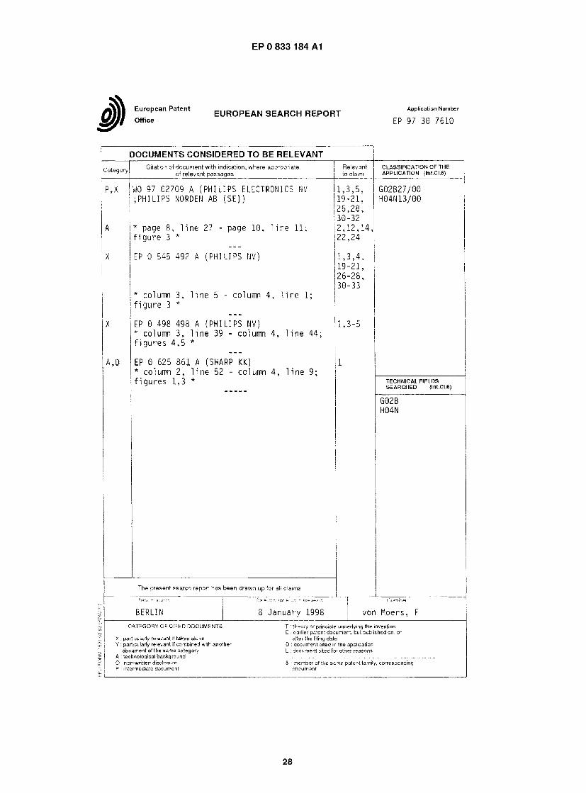
EUROPEAN SEARCH REPORT Application Number EP 97 30 7610
DOCUMENTS CONSIDERED TO BE RELEVANT
Category Citation of document with indication, where appropriate, of relevant passages Relevant to claim
CLASSIFICATION OF THE APPLICATION (lnt.Ci.6)
p.x
A,D
WO 97 G2709 A (PHILIPS ELECTRONICS NV ; PHI LI PS NORDEN AB (SE))
* page 8, line 27 - page 10, line 11; figure 3 *
EP 0 545 492 A (PHILIPS NV)
* column 3, line 5 - column 4, line 1; figure 3 *
EP 0 498 498 A (PHILIPS NV) * column 3, line 39 - column 4, line 44; figures 4,5 *
EP 0 625 861 A (SHARP KK) * column 2, line 52 - column 4, line 9; figures 1,3 *
The present search report has been drawn up for all claims
1,3,5, 19-21, 26,28, 30-32 2,12,14, 22,24
1,3,4, 19-21, 26-28, 30-33
1,3-5
G02B27/G0 H04N13/00
TECHNICAL FIELDS SEARCHED (lnt.CI.6) 602B H04N
BERLIN 8 January 1998 von Moers, F CATEGORY OF CITED DOCUMENTS
X : particularly relevant if taken alone Y : particularly relevant if combined wrrh another document of the same category A : technological background O ' non-written disclosure P : intermediate document
T : theory or principle underlying the invention E earlier patent document, but published an, or after the filing date D : document cited in the application L : document cited for other reasons & ' member of the same patent family, corresponding document
28