Embed Size (px)
Citation preview
Electrochromic Diffraction fromNanopatterned Poly(3-hexylthiophene)Yuna Kim, Yoonjung Kim, Sehwan Kim, and Eunkyoung Kim*
Department of Chemical and Biomolecular Engineering, Yonsei University, 262 Seongsanno, Seodaemun-gu, Seoul 120-749, Korea
Electronic devices based on conduct-ing polymers (CP) have attracted con-siderable attention because conju-
gated polymers can be easily processed
with inexpensive technologies at low tem-
peratures. The potential applications of CPs
for organic electronic devices include solar
cells, light-emitting diodes (LEDs), electro-
chromic (EC) devices, photodiodes, transis-
tors, and biosensors.1�5 The development of
a faster and more integrated electrical or
optical response has become a high prior-
ity. As such, the modification of an electro-
active surface by nanostructures has been
researched for switching or sensing
devices.6�8
In electrochromic devices (ECDs), elec-
trons are injected or extracted under an ap-
plied electric field while charge balancing
counterions are simultaneously transported
into or out of the EC layer.9,10 The transport
of electrons and ions is directly related to EC
properties such as coloration efficiency and
response time.9�11 Recently, fast response
times and high color contrast have report-
edly been achieved with EC devices fabri-
cated with a nanostructured EC electrode
since the nanostructures can provide a large
surface area. The increased surface area fa-
cilitates ion transport and provides more ac-
cessible reacting sites for the charge/dis-
charge process.8,10,12 Such a nanostructured
EC electrode can be prepared through
layer-by-layer (LBL) deposition11,13 or by
adopting nanotemplates such as anodized
aluminum oxide (AAO),14 TiO2 nanoparti-
cles,8 Si nanowires,10 and block copolymer
templates.15 As the charge transport in an
EC device occurs vertically between the
working and counter electrode, the design
of a vertical EC nanostructure is indeed a
challenge.
Various methods of fabricating conduct-ing polymer nanostructures have been re-ported. Of the methods used, soft lithogra-phy using solution-processable conductingpolymers can efficiently produce nanostruc-tures with a large area.16�19 However, its ap-plication to ECDs is rare.18,19 In a report onthe effect of nanoimprinting on the electro-chromic properties of PEDOT:PSS,18 im-provements in both the response time andcoloration efficiency were attained. How-ever, to the best of our knowledge, thereare no published reports on the direct ef-fect of patterning in terms of charge trans-port through the patterned structures.
In this study, an EC device based on ananopatterned EC electrode was fabri-cated. The EC electrode was prepared by di-rectly nanoimprinting a pristine poly(3-hexylthiophene) (P3HT) film with ananopattern replicated polydimethylsilox-ane (PDMS) mold. Films with line gratings(1D) and pillars (2D) were examined to ex-plore the charge transport and optical
*Address correspondence [email protected].
Received for review July 14, 2010and accepted August 16, 2010.
Published online August 23, 2010.10.1021/nn1016378
© 2010 American Chemical Society
ABSTRACT Poly(3-hexylthiophene) (P3HT) films were patterned by a soft lithography technique using a
nanopatterned polydimethylsiloxane (PDMS) mold to generate one-dimensional (1D) grating and two-
dimensional (2D) crossed line pillar patterns. The redox currents (ip) were significantly increased due to the
facilitated diffusion of ClO4� counterions associated with redox processes at the P3HT electrode as analyzing
cyclic voltammetry (CV) was performed at different scan rates (�). It was found that the diffusion coefficient (Df,
cm2 s�1) for ion diffusion in the patterned electrode was much larger than that of the pristine P3HT electrode.
Furthermore, the value of Df in the 2D electrode was three times higher than that in a pristine film. As a result of
such facilitated charge transport, the electrochromic (EC) properties of the patterned P3HT electrode were greatly
enhanced and dependent on the dimension of the pattern. Thus, the electrochromic efficiency (Ee), including the
coloration (Ec) and bleaching efficiencies (Eb), was higher as the dimension of the pattern was increased; Ee was
maximized in the 2D patterned P3HT film. In a patterned cell, electrochromic diffraction was reversibly observed
with a switching efficiency (RDE) of 2 and 2.5 for the 1D and 2D patterned cells, respectively.
KEYWORDS: patterning · poly(3-hexylthiophene) · electrochromic · nanoimprint · PDMS
ARTIC
LE
www.acsnano.org VOL. 4 ▪ NO. 9 ▪ 5277–5284 ▪ 2010 5277
properties of the patterned EC devices. While P3HT is arepresentative hole transporting material and is fre-quently used for organic devices such as photovoltaicsand transistors,20,21 its application to electrochromic de-vices is relatively rare despite its unique electrochro-mic properties and the easy processability.22
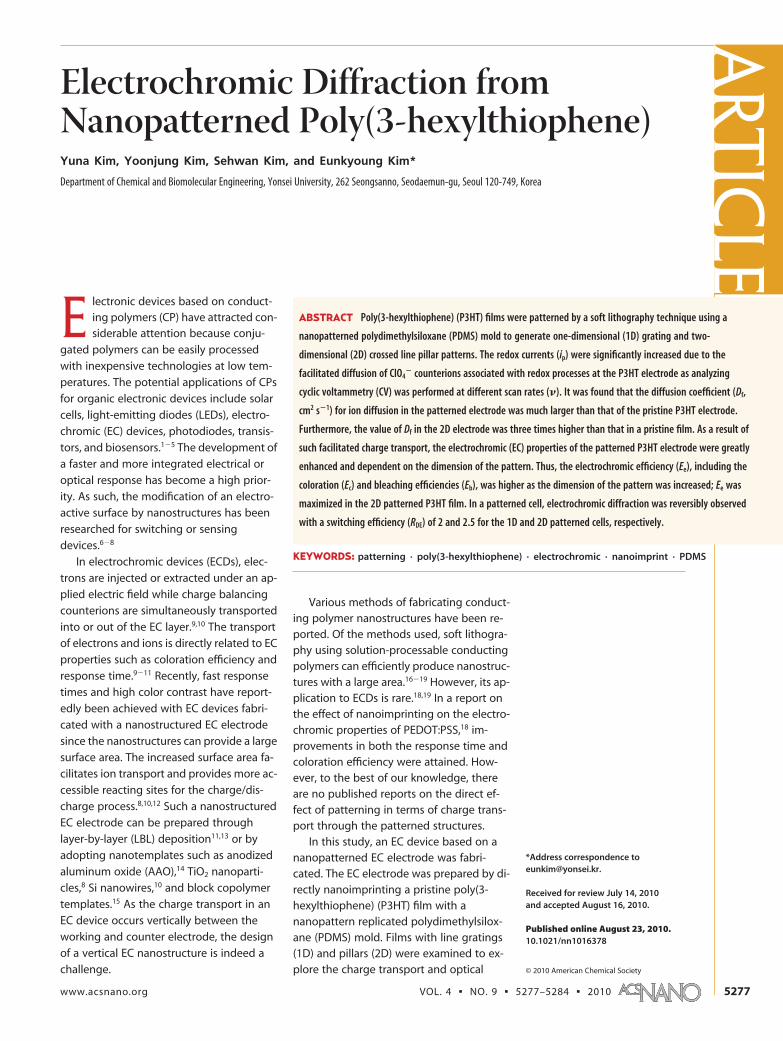
RESULTS AND DISCUSSIONPatterning of P3HT in 1D and 2D by PDMS Imprinting. P3HT
films were nanopatterned via soft lithography per-formed at room temperature. A PDMS mold consistingof periodic 170 nm width lines separated by 80 nm widegaps was employed in the nanopatterning process (Fig-ure S1, Supporting Information). Nanogratings (1D)were first patterned on a P3HT film by a single imprint-ing without any pressure. However, the depth of thegratings was rather small: 25 nm as determined fromAFM. Under a pressure of 5 kg, the depth in the 1D pat-terning process was increased to 47 nm. Thus, 1D and2D patterning was carried out under pressure. As veri-fied by AFM measurements, 1D nanogratings of thePDMS in a 1 � 1 cm2 area were successfully and homo-geneously transferred to the entire area of the P3HTfilm. The width and gap between the lines were 362and 110 nm, respectively (Figure 1). The nanogratingson the P3HT were wider in period and shallower indepth than those of the PDMS master.
Additional contact pressing in a 90° direction underthe same pressure produced nanopillars (2D) on thesingle patterned P3HT. Nanopillar patterns (2D) were
generated with dimensions of 380 nm in width, 60 nm
in height, and a pillar separation of about 80 nm in the
double-pressed area. As shown in Figure 2, the edge im-
age clearly traced the first (1D) and second (but single-
pressed) patterns, as well as the second pattern at the
crossed (double-pressed) area. In the area pressed sec-
ond with a single press, the height was slightly lower
(�40 nm) than the area pressed first. This was possibly
due to the evaporation of residual solvent. The height
was increased in the cross (double) patterned area.
The average roughness (Ra) values in a 5 �m � 5 �m
area were 1.1, 11.3, and 18.3 nm for the pristine (0D),
1D, and 2D patterned films, respectively. This indicates
Figure 1. Atomic force microscope (AFM) images of single patterned P3HT film fabricated by imprinting at room temperature (A)and double patterned P3HT film (B) fabricated by subsequent additional imprinting at 90° on single patterned P3HT film. (C) Pris-tine P3HT film (0D), and (D) cross-sectional profiles of (A) and (B).
Figure 2. Edge AFM image of 2D patterned P3HT film thatwas first (a, 1D) and second (b, but single-pressed) pat-terned, and second patterned at the crossed (c, double-pressed) area (inset: 3D image).
ART
ICLE
VOL. 4 ▪ NO. 9 ▪ KIM ET AL. www.acsnano.org5278
that the roughness of the film increased as the dimen-
sion of the pattern increased. Such a scenario is possi-
bly due to increased ordering in the P3HT domain. It has
been reported that P3HT chain alignment can be en-
hanced during nanograting imprinting on a P3HT film.
The chain alignment is induced by polymer flow to
nanocavities, thus generating high degree (100) chain
alignment.23 After patterning, the surface area of the
films increased to 25.2, 25.7, and 26.8 �m2 for the pris-
tine (0D), 1D, and 2D patterned films, respectively. The
surface areas attained from the simulation using Matlab
were in good agreement with the AFM results as 25.4
and 26.9 �m2 for the 1D and 2D patterns, respectively,
when the geometry of the column (1D) and pillars (2D)
were assumed to be triangular and conical structure,
respectively.
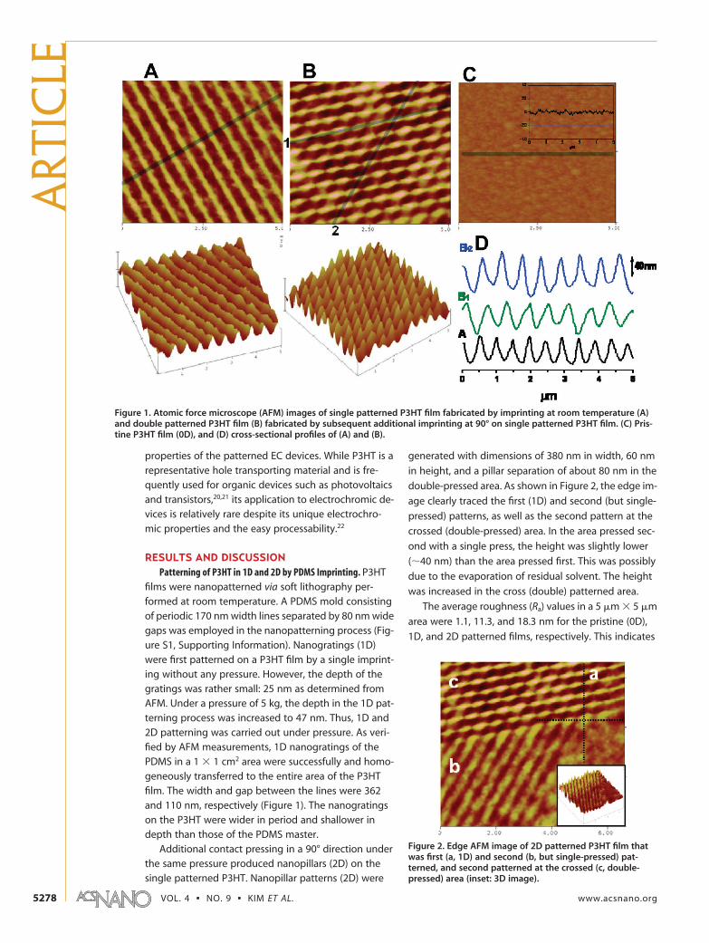
Electrochemical Properties of Nanopatterned P3HT. Cyclic
voltammetry (CV) measurements for the pristine (0D),
1D, and 2D patterned P3HT films were performed in a
three-electrode system using a solution of 0.1 M LiClO4
in acetonitrile and a scan rate of 10 mV/s from 0 to 1.3 V
(Figure 3A). All films exhibited several redox peaks cen-
tered at �0.49 and 0.83 V (vs Ag/AgCl). A transition be-
tween the polaronic and bipolaronic states22 was ob-
served. This transition is detailed in the following
expression:
In eq 1, ClO4� is a counteranion and e� denotes an elec-
tron. It should be noted that the redox peaks of the 1D
and 2D patterned films were shifted with a much higher
intensity than those of the unpatterned film (0D). It
has been reported that P3HT films with a high degree
of ordering or regioregularity exhibit larger peak cur-
rents with a peak shift.22,24,25 Thus, P3HT chain align-
ment may be enhanced during nanoimprinting on a
P3HT film, as nanoconfinement induces chain align-
ment in P3HT nanostructures and generates a high
degree (100) of chain alignment.23 The X-ray diffraction(XRD) results showed that the intensity decrease of the(100) peak at 5.2° was 24% (1D) and 61% (2D) (FigureS2A, Supporting Information). This result is in goodagreement with results from the literature regardingchanges in the out-of-plane detecting mode P3HT andmay be attributed mainly to changes in P3HT chain or-dering edge-on to the vertical ordering.23 In addition,the (100) diffraction peak was shifted from 5.15° (0D) to5.20° (1D) and 5.25° (2D), and the interlayer spacing de-termined from the Bragg equation was shifted from17.15 to 16.98 and 16.82 Å for 0D, 1D, and 2D, respec-tively. The P3HT chain spacing became smaller afternanopatterning, thus it provided lower resistance tocharge carriers to transport through the polymerchains.22 The increase in absorbance at the shoulderband (�570 nm) in the nanoimprinted gratings (Fig-ure S2B) is due to the increased ���* stacking and in-terchain interactions between P3HT chains.23,26 The���* chain alignment could be quantified by compar-ing absorbance ratios at �590 nm with absorbancemaxima (�530 nm) in different samples. The absor-bance ratio was 0.49 for 0D and increased to 0.54 for1D and 0.67 for 2D. This indicates that the ���* inter-chain stacking was improved by nanopatterning, butthe change was small (less than 30%).
The major contribution to the increased currentarises from the extra shoulder peak (0.5�0.8 V) be-tween the first and second redox processes. The shoul-der peak is indicative of the formation of new polymerdomains that may facilitate charge transport throughthe P3HT electrode. This redox process is reversible overrepeated voltammetric scans with no electrochemicaldegradation during cycles between the polaronic andbipolaronic (neutral and oxidized) states. As the redoxpeaks consisted of two peaks plus shoulder peaks, all ofthe CV measurements were deconvoluted (R2 � 0.999)based on Gaussian peaks (Figure S3, Supporting Infor-mation) to quantify the peak current and determinecharge transport at the electrode nanopatterned in dif-ferent dimensions.
In an electrochemical process that is linear-diffusion-driven, the peak current is related to the electrode area
Figure 3. (A) Cyclic voltammogram of P3HT films at 10 mV/s. (B) Plot of cathodic and anodic peak current according to thesquare root of the scan rate (v0.5).
P3HT0 +
ClO4-
(neutral){\}
Ox(-e-)
red(+e-)P3HT+•ClO4
-
(polaron, radical cation){\}
Ox(-e-)
red(+e-)P3HT2+2ClO4
-
(bipolaron, dication)
(1)
ARTIC
LE
www.acsnano.org VOL. 4 ▪ NO. 9 ▪ 5277–5284 ▪ 2010 5279
and the square root of the scan rate (�1/2) according to
the Randles�Sevcik equation:27
In eq 2, ip is the peak current, n is the number of elec-
tron transfer, Df (cm2 s�1) is the diffusion coefficient, A
is the electrode area (cm2), C is the solution concentra-
tion (mol cm�3), and � is the scan rate (V s�1). By plot-
ting the anodic and cathodic peak current obtained at
�0.57 and �0.54 V against �1/2 for both the pristine and
nanostructured electrodes, linear relationships (shown
in Figure 3B) were observed. Both the anodic and ca-
thodic currents were linearly correlated to �1/2, which in-
dicates that electrochemical doping of the entire P3HT
film occurred with no irreversible electrochemical reac-
tion. Furthermore, the linear relationship of ip against
�1/2 suggests that the behavior of the electrochemical
processes at the P3HT electrode is mainly controlled by
the diffusion of ClO4� counterions associated with the
redox processes at the P3HT electrode. The Df values for
the patterned electrodes were determined from the
slope in Figure 3B; they are summarized in Table 1. The
Df values for the oxidation of the electrodes are larger
than those of the reduction process. In the electro-
chemical doping process of a polythiophene film, ClO4�
ions penetrate into the polymer and promote move-
ment in nearby polymer molecules, which favors pen-
etration of further ClO4� into the polymer. Movement
and ionic penetration proceed on the surface in a sig-
moidal fashion, and thus, the charge transport is facili-
tated. Upon dedoping in the reduction step, the orien-
tation of the P3HT chains switches from a “lying-down”
configuration to an “on-edge” configuration with the
alkyl chains being normal to the electrode surface.28
Thus, in the reduction, it takes more time to remove
the ions that have penetrated into the polymer layer
into the electrolyte solution. The Df values for reduc-
tion are therefore smaller than those for oxidation. In-
terestingly, the diffusion coefficient for the patterned
electrode was much larger than that of the unpatterned
electrode. Furthermore, Df was larger as the dimension
of the pattern was increased (Table 1). The Df for the 2D
patterned electrode was the largest among the P3HT
electrodes. The diffusion coefficient for the oxidation
process in 2D reached 6.67 � 10�9 cm2/s, which is three
times higher than that of the pristine film. The Df value
for the dedoping of ClO4� counterions for coloration
(3.36 � 10�9 cm2/s) was also higher in the 2D patterned
electrode. The diffusion coefficients in this work are
larger than the reported values for P3HT (10�10�10�14
cm2/s) films in contact with liquid electrolytes.29,30 This is
possibly due to the ordering of P3HT in this work
through patterning. In addition, the Df value of the 2D
patterned P3HT is an order of magnitude higher than
those of conducting polymer films based on PEDOT31,32
for electrochromic devices. Therefore, as discussed in
the literature,33,34 the electronic response of a conduc-
tive polymer-based device may improve as charge
transport through the nanostructured electrode is en-
hanced due to fast diffusion at the electrode. To prove
such a concept, the nanostructured electrodes were in-
corporated into an electrochromic (EC) window and
test for diffraction control.
Electrochromic (EC) Properties of Nanostructured P3HT
Electrodes. Transmissive-type EC devices were prepared
with P3HT films as a working electrode and ITO glass as
a counter electrode. The liquid electrolyte solution de-
scribed in Figure 3A was introduced between the two
electrodes. The EC devices exhibited a reversible color
change from red to transparent blue when �2 to 2 V
was applied. The EC response required a larger poten-
tial step than was expected from the solution CV. This
reflects the fact that the CV of the two-electrode system
exhibited broad redox peaks at �2 and �2 V for oxida-
tion and reduction, respectively, for the 2D patterned
EC electrode (Figure S4, Supporting Information). As
evident in Table 2, the color change was smaller when
�1/2 or �2.5/2.5 V was applied to the EC devices. This
indicates that the color change corresponds to redox
reactions that consume charges generated at the peak
potential in the two-electrode CV. The UV�vis absor-
bance changes of the EC cells from a neutral (�2 V) to
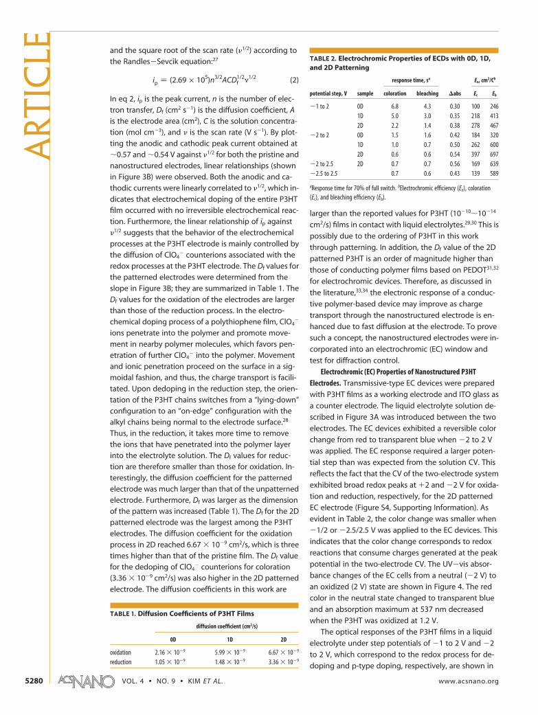
an oxidized (2 V) state are shown in Figure 4. The red
color in the neutral state changed to transparent blue
and an absorption maximum at 537 nm decreased
when the P3HT was oxidized at 1.2 V.
The optical responses of the P3HT films in a liquid
electrolyte under step potentials of �1 to 2 V and �2
to 2 V, which correspond to the redox process for de-
doping and p-type doping, respectively, are shown in
TABLE 1. Diffusion Coefficients of P3HT Films
diffusion coefficient (cm2/s)
0D 1D 2D
oxidation 2.16 � 10�9 5.99 � 10�9 6.67 � 10�9
reduction 1.05 � 10�9 1.48 � 10�9 3.36 � 10�9
TABLE 2. Electrochromic Properties of ECDs with 0D, 1D,and 2D Patterning
response time, sa Ee, cm2/Cb
potential step, V sample coloration bleaching �abs Ec Eb
�1 to 2 0D 6.8 4.3 0.30 100 2461D 5.0 3.0 0.35 218 4132D 2.2 1.4 0.38 278 467
�2 to 2 0D 1.5 1.6 0.42 184 3201D 1.0 0.7 0.50 262 6002D 0.6 0.6 0.54 397 697
�2 to 2.5 2D 0.7 0.7 0.56 169 639�2.5 to 2.5 0.7 0.6 0.43 139 589
aResponse time for 70% of full switch. bElectrochromic efficiency (Ee), coloration(Ec), and bleaching efficiency (Eb).
ip ) (2.69 × 10⁵)n3/2ACDf1/2ν1/2 (2)
ART
ICLE
VOL. 4 ▪ NO. 9 ▪ KIM ET AL. www.acsnano.org5280
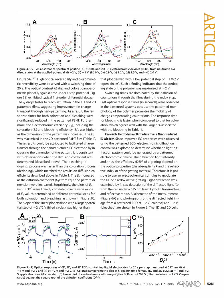
Figure 5A.28,35 High optical reversibility and coulommet-ric reversibility were observed with a switching time of20 s. The optical contrast (abs) and coloratioampero-metric plot of ip against time under a step potential (Fig-ure 5B) exhibited typical first-order differential decay.The ip drops faster to reach saturation in the 1D and 2Dpatterned films, suggesting improvement in chargetransport through nanopatterning. As a result, the re-sponse times for both coloration and bleaching weresignificantly reduced in the patterned P3HT. Further-more, the electrochromic efficiency (Ee), including thecoloration (Ec) and bleaching efficiency (Eb), was higheras the dimension of the pattern was increased. The Ee
was maximized in the 2D patterned P3HT film (Table 2).These results could be attributed to facilitated chargetransfer through the nanostructured EC electrode by in-creasing the dimension of the pattern. It is consistentwith observations when the diffusion coefficient wasdetermined (described above). The bleaching (p-doping) process was faster than the coloration process(dedoping), which matched the results on diffusion co-efficients described above in Table 1. The Ee increasedas the diffusion coefficient (Df) from eq 2 and pattern di-mension were increased. Surprisingly, the plots of Ee
versus Df0.5 were linearly correlated over a wide range
of Ee values determined at different potential steps forboth coloration and bleaching, as shown in Figure 5C.The slope of the linear plot attained with a larger poten-tial step of �2 V/2 V (filled circles) was higher than
that plot derived with a low potential step of �1 V/2 V(open circles). Such a finding indicates that the dedop-ing state of the polymer was maximized at �2 V.
Switching times are dominated by the diffusion ofcounterions through the films during the redox step.Fast optical response times (in seconds) were observedin the patterned systems because the patterned mor-phology of the polymer promotes the mobility ofcharge compensating counterions. The response timefor bleaching is faster when compared to that for color-ation, which agrees well with the larger Df associatedwith the bleaching in Table 1.
Reversible Electrochromic Diffraction from a NanostructuredEC Window. Since improved EC properties were observedusing the patterned ECD, electrochromic diffractioncontrol was explored to determine whether a light dif-fraction pattern could be generated by a patternedelectrochromic device. The diffraction light intensityand, thus, the efficiency (DE)36 of a grating depend onthe optical properties (the absorptivity k and the refrac-tive index n) of the grating material. Therefore, it is pos-sible to use an electrochemical stimulus to modulatethe DE of a redox-active grating. Light diffraction wasexamined by in situ detection of the diffracted light (Id)from the cell under a 635 nm laser, by both transmittiveand reflective mode. A schematic of the measurement(Figure 6A) and photographs of the diffracted light im-age from a patterned ECD at �2 V (colored) and �2 V(bleached) are shown in Figure 6. The 1D and 2D cells
Figure 4. UV�vis absorbance spectra of pristine (A), 1D (B), and 2D (C) electrochromic devices (ECDs) from neutral to oxi-dized states at the applied potential; (i) �2 V, (ii) �1 V, (iii) 0 V, (iv) 0.9 V, (v) 1.2 V, (vi) 1.5 V, and (vii) 2.0 V.
Figure 5. (A) Optical responses of 0D, 1D, and 2D ECDs containing liquid electrolytes for 20 s per step measured at 537 nm; (i) at�1 V and �2 V and (ii) at �2 V and �2 V. (B) Coloratioamperometric plot of ip against time for 0D, 1D, and 2D ECDs at �1 and �2V applications for 20 s per step. (C) Linear plot of electrochromic efficiency (Ee) for ECDs at �2 V/2 V (filled circle) and �1 V/2 V (opencircle) against the square root of the diffusion coefficient (Df
0.5).
ARTIC
LE
www.acsnano.org VOL. 4 ▪ NO. 9 ▪ 5277–5284 ▪ 2010 5281
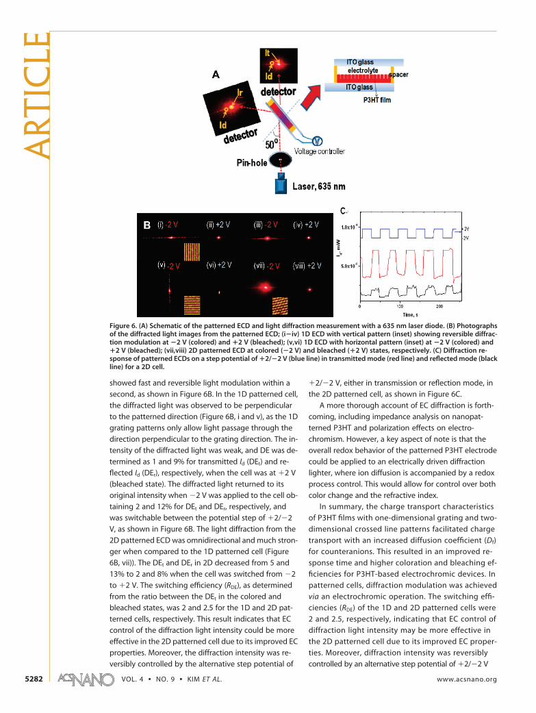
showed fast and reversible light modulation within a
second, as shown in Figure 6B. In the 1D patterned cell,
the diffracted light was observed to be perpendicular
to the patterned direction (Figure 6B, i and v), as the 1D
grating patterns only allow light passage through the
direction perpendicular to the grating direction. The in-
tensity of the diffracted light was weak, and DE was de-
termined as 1 and 9% for transmitted Id (DEt) and re-
flected Id (DEr), respectively, when the cell was at �2 V
(bleached state). The diffracted light returned to its
original intensity when �2 V was applied to the cell ob-
taining 2 and 12% for DEt and DEr, respectively, and
was switchable between the potential step of �2/�2
V, as shown in Figure 6B. The light diffraction from the
2D patterned ECD was omnidirectional and much stron-
ger when compared to the 1D patterned cell (Figure
6B, vii)). The DEt and DEr in 2D decreased from 5 and
13% to 2 and 8% when the cell was switched from �2
to �2 V. The switching efficiency (RDE), as determined
from the ratio between the DEt in the colored and
bleached states, was 2 and 2.5 for the 1D and 2D pat-
terned cells, respectively. This result indicates that EC
control of the diffraction light intensity could be more
effective in the 2D patterned cell due to its improved EC
properties. Moreover, the diffraction intensity was re-
versibly controlled by the alternative step potential of
�2/�2 V, either in transmission or reflection mode, in
the 2D patterned cell, as shown in Figure 6C.
A more thorough account of EC diffraction is forth-
coming, including impedance analysis on nanopat-
terned P3HT and polarization effects on electro-
chromism. However, a key aspect of note is that the
overall redox behavior of the patterned P3HT electrode
could be applied to an electrically driven diffraction
lighter, where ion diffusion is accompanied by a redox
process control. This would allow for control over both
color change and the refractive index.
In summary, the charge transport characteristics
of P3HT films with one-dimensional grating and two-
dimensional crossed line patterns facilitated charge
transport with an increased diffusion coefficient (Df)
for counteranions. This resulted in an improved re-
sponse time and higher coloration and bleaching ef-
ficiencies for P3HT-based electrochromic devices. In
patterned cells, diffraction modulation was achieved
via an electrochromic operation. The switching effi-
ciencies (RDE) of the 1D and 2D patterned cells were
2 and 2.5, respectively, indicating that EC control of
diffraction light intensity may be more effective in
the 2D patterned cell due to its improved EC proper-
ties. Moreover, diffraction intensity was reversibly
controlled by an alternative step potential of �2/�2 V
Figure 6. (A) Schematic of the patterned ECD and light diffraction measurement with a 635 nm laser diode. (B) Photographsof the diffracted light images from the patterned ECD; (i�iv) 1D ECD with vertical pattern (inset) showing reversible diffrac-tion modulation at �2 V (colored) and �2 V (bleached); (v,vi) 1D ECD with horizontal pattern (inset) at �2 V (colored) and�2 V (bleached); (vii,viii) 2D patterned ECD at colored (�2 V) and bleached (�2 V) states, respectively. (C) Diffraction re-sponse of patterned ECDs on a step potential of �2/�2 V (blue line) in transmitted mode (red line) and reflected mode (blackline) for a 2D cell.
ART
ICLE
VOL. 4 ▪ NO. 9 ▪ KIM ET AL. www.acsnano.org5282
in the 2D patterned cell either in transmittive or re-flected mode. Future patterning studies of thin filmsfabricated from P3HT or its derivatives will contrib-ute to an improved understanding of charge trans-
port in nanostructured conductive polymers and fos-ter the development of advanced EC devices withimproved optical, ionic, and electronic transportproperties.
METHODSPoly(3-hexylthiophene) (P3HT, Mw 25 000 g · mol�1) was
purchased from Rieke Metals Inc. 1,2-Dichlorobenzene was ob-tained from Sigma-Aldrich. PDMS and a curing agent (Sylgard184) were purchased from the Dow Corning Corporation.Lithium perchlorate and acetonitrile were obtained from Sigma-Aldrich.
A 2 wt % P3HT solution in 1,2-dichlorobenzene was spin-coated at 700 rpm for 40 s on an ITO glass electrode (13�/square). A P3HT nanopatterned film was then generated viasoft lithography,18 a simple contact-pressing method that em-ploys a nanopattern replicated PDMS mold. A nanopatternedphotoresist template on a silicon wafer was provided by KeumhoPetrochemicals and used for the replication (Figure S1, Support-ing Information). The template consisted of nanogratings in a 1cm � 1 cm area with a width of 250 nm and a height of 90 nm.The gap between the gratings was 15 nm. A detailed PDMS moldfabrication method is described elsewhere.37 A replicated PDMSnanograting mold (1.3 g in weight) consisting of periodic 170 nmwidth lines separated by 80 nm wide gaps was introduced forthe nanoimprinting. The trenches of the gratings were 80 nm indepth. Nanoimprinting was carried out at room temperature.P3HT nanogratings (1D) were obtained through a single imprint-ing. After full contact between the P3HT film and the PDMS pat-terned area was established, pressing was performed for 3 minwith PDMS mold at a pressure of 5 kg. This resulted in a wet sur-face flow-induced pattern. Additional contact pressing in a 90°direction was carried out under pressure of 5 kg for 5 min atroom temperature to produce nanopillars (2D) on the surfaceof single patterned P3HT. The pristine and patterned films wereboth annealed under vacuum at 100 °C for 10 min to evaporateresidual solvent in the film.
A conventional three-electrode system consisting of theP3HT-coated ITO glass as the working electrode and Ag/AgCland Pt wire as the counter electrode was used for cyclic voltam-metry measurements. Lithium perchlorate (LiClO4, 0.1 M) in ace-tonitrile was employed as a supporting electrolyte. An electro-chromic device with two electrodes was fabricated using P3HT-coated ITO glass as the working electrode and bare ITO glass asthe counter electrode. A liquid electrolyte containing 0.1 M LiC-lO4 in acetonitrile was isolated between the two electrodes by aspacer.
The conductivities of the 0D, 1D, and 2D patterned P3HTfilms were examined using a top-contact four-point probe. Con-ductivity was determined to be 0.10, 0.11, and 0.13 S/cm for0D, 1D, and 2D samples, values that are comparable to previ-ously reported values.38 The pattern-induced conductivity incre-ment was 30% (30 mS/cm). This small change in conductivitycaused by patterning may be attributed to the unpatternedP3HT part of the film. As shown in Figure 1D, the maximumheight of the gratings is 60 nm, while the thickness of the P3HTfilm was 100 nm. Thus, the thickness of the unpatterned P3HT is�40 nm, which connects the P3HT conductive channel to yieldsmall conductivity change.
Electrochromic properties were determined by an in situspectro-electrochemical setup.8�12 The coloration efficiency andresponse time of the ECDs were determined at the absorptionmax under a square-wave switching potential using a chrono-coulometry in liquid electrolyte having an EC window size of 1.0� 1.0 cm2. The EC response time for coloration and bleachingwas determined at a 70% absorption change11,12 under the givenstep potentials. The electrochromic efficiency (Ee) including thecoloration and bleaching efficiency was determined by dividingthe abs by the injected/ejected charge per unit area.39
A 635 nm diode laser with an intensity of 2.1 mW was usedto measure the diffraction from the patterned electrochromic de-
vices at colored and bleached states (Figure 6A). The intensitiesof the reflected (Ir), transmitted (It), and Ia (“Id � Ir” or “Id � It”) lightwere determined using a photodetector. Id was calculated asthe difference between the Ia and It or Ir. UV�vis spectra were at-tained with an Avaspec-2048 fiber optic spectrometer. The nano-pattern transfer from the PDMS stamp to the composite filmswas carried out using Nanoimprint (HIS-400U, Hutem Inc.). Thethickness of the polymer films was determined via profilometrymeasurements performed with an Alpha Step profilometer (Ten-cor Instruments, Alpha-Step IQ). The accuracy of the profilome-ter was 1 nm. Atomic force microscopy (AFM) was carried out intapping mode at room temperature with a Dimension 3100 SPMequipped with a Nanoscope IVa (Digital Instruments, Santa Bar-bara, CA).
Acknowledgment. This work was supported by the NationalResearch Foundation (NRF) grant funded by the Korea govern-ment (MEST) through the Active Polymer Center for Pattern Inte-gration (No. R11-2007-050-00000-0) and Ministry of KnowledgeEconomy (MKE), New & Renewable Energy Technology Develop-ment Program.
Supporting Information Available: Atomic force microscope(AFM) images are available for the nanopattern master; XRDgraphs and UV�vis spectra of pristine (0D), 1D, and 2D pat-terned P3HT film; analyses of redox peaks based on Gaussianmultipeak deconvolution of cyclic voltammograms of 0D, 1D,and 2D patterned P3HT films using Origin 7.5; and cyclic voltam-mogram of two-electrode P3HT-based ECD scanning between�2 to 2 V at 0.1 V/s. This material is available free of charge viathe Internet at http://pubs.acs.org.
REFERENCES AND NOTES1. Yu, G.; Gao, J.; Hummelen, J. C.; Wudl, F.; Heeger, A. J.
Polymer Photovoltaic Cells: Enhanced Efficiencies via aNetwork of Internal Donor�Acceptor Heterojunctions.Science 1995, 270, 1789–1791.
2. Kim, Y.; Do, J.; Kim, J.; Yang, S. Y.; Malliaras, G. G.; Ober,C. K.; Kim, E. A Glucose Sensor Based on an OrganicElectrochemical Transistor Structure Using a VaporPolymerized Poly(3,4-ethylenedioxythiophene) Layer. Jpn.J. Appl. Phys. 2010, 49, 01AE10-1–01AE10-10.
3. Kim, Y.; Yun, C.; Jadhav, P.; You, J.; Kim, E. Emissive PatternFormation by the Photoreaction of Poly(p-phenylenevinylene). Curr. Appl. Phys. 2009, 9, 1088–1092.
4. Kim, D. C.; Lee, T. W.; Lee, J. E.; Kim, K. H.; Cho, M. J.; Choi,D. H.; Han, Y. D.; Cho, M. Y.; Joo, J. S. New SemiconductingMulti-branched Conjugated Molecules Bearing 3,4-Ethylenedioxythiophene-Based Thiophenyl Moieties forOrganic Field Effect Transistor. Macromol. Res. 2009, 17,491–498.
5. Kim, J.; Kim, Y.; Kim, E. Electrochromic Pattern Formationby Photo Cross-Linking Reaction of PEDOT Side Chains.Macromol. Res. 2009, 17, 791–796.
6. Dobrokhotov, V. V.; McIlroy, D. N.; Norton, M. G.; Berven,C. A. Transport Properties of HybridNanoparticleONanowire Systems and Their Application toGas Sensing. Nanotechnology 2006, 16, 4135–4142.
7. Ziebarth, J. M.; Saafir, A. K.; Fan, S.; McGehee, M. D.Extracting Light from Polymer Light-Emitting DiodesUsing Stamped Bragg Gratings. Adv. Funct. Mater. 2004,14, 451–456.
8. Baek, J.; Kim, Y.; Kim, E. Growth and ElectrochromicProperties of PEDOT Layer on TiO2 Nanoparticles. J.Nanosci. Nanotechnol. 2008, 8, 4851–4855.
ARTIC
LE
www.acsnano.org VOL. 4 ▪ NO. 9 ▪ 5277–5284 ▪ 2010 5283

9. Kim, Y.; Kim, E. Complementary Electrochromic Windowswith Conductive Nanocomposite Thin Films. Curr. Appl.Phys. 2008, 8, 752–754.
10. Kim, Y.; Baek, J.; Kim, M.-H.; Choi, H.-J.; Kim, E.Electrochromic Nanostructures Grown on a SiliconNanowire Template. Ultramicroscopy 2008, 108,1224–1227.
11. Kim, Y.; Kim, E. Electrochromic Properties of NanochromicWindows Assembled by the Layer-by-Layer Self-AssemblyTechnique. Curr. Appl. Phys. 2006, 6, e202–e205.
12. Kim, Y.; Yang, S. Y.; Kim, E. Electrochromic Properties ofAsymmetric 4,4=-Bipyridinium Nanocomposites withInorganic Nanoparticles. J. Nanosci. Nanotechnol. 2010, 10,263–268.
13. Kim, E.; Jung, S. Layer-by-Layer Assembled ElectrochromicFilms for All-Solid-State Electrochromic Devices. Chem.Mater. 2005, 17, 6381–6387.
14. Cho, S. I.; Kwon, W. J.; Choi, S.-J.; Kim, P.; Park, S.-A.; Kim, J.;Son, S. J.; Xiao, R.; Kim, S.-H.; Lee, S. B. Nanotube-BasedUltrafast Electrochromic Display. Adv. Mater. 2005, 17,171–175.
15. Brezesinski, T.; Rohlfing, D. F.; Sallard, S.; Antonietti, M.;Smarsly, B. M. Highly Crystalline WO3 Thin Films withOrdered 3D Mesoporosity and Improved ElectrochromicPerformance. Small 2006, 2, 1203–1211.
16. Zhang, F.; Nyberg, T.; Inganas, O. Conducting PolymerNanowires and Nanodots Made with Soft Lithography.Nano Lett. 2002, 2, 1373–1377.
17. Beh, W. S.; Kim, I. T.; Qin, D.; Xia, Y.; Whitesides, G. M.Formation of Patterned Microstructures of ConductingPolymers by Soft Lithography, and Applications inMicroelectronic Device Fabrication. Adv. Mater. 1999, 11,1038–1041.
18. Admassieaz, S.; Inganas, O. Electrochromism in DiffractiveConducting Polymer Gratings. J. Electrochem. Soc. 2004,151, H153–H157.
19. Choi, J.; Kumar, A.; Sotzing, G. A. NanopatternedElectrochromic Conjugated Poly(terthiophene)s viaThermal Nanoimprint Lithography of Precursor Polymer. J.Macromol. Sci. A 2007, 44, 1305–1309.
20. Jeffries-El, M.; McCullough, R. D. Conjugated Polymers:Theory, Synthesis, and Characterizations. In Handbook ofConducting Polymers; Skotheim, T. A., Reynolds, J. R., Eds.;CRC Press: Boca Raton, FL, 2007; pp 9-1�9-2.
21. Sirringhaus, H.; Brown, P. J.; Friend, R. H.; Nielsen, M. M.;Bechgaard, K.; Langeveld-Voss, B. M. W.; Spiering, A. J. H.;Janssen, R. A. J.; Meijer, E. W.; Herwig, P.; et al. Two-Dimensional Charge Transport in Self-Organized, High-Mobility Conjugated Polymers. Nature 1999, 401, 685–688.
22. Huang, J.-H.; Yang, C.-Y.; Hsu, C.-Y.; Chen, C.-L.; Lin, L.-Y.;Wang, R.-R.; Ho, K.-C.; Chu, C.-W. Solvent-Annealing-Induced Self-Organization of Poly(3-hexylthiophene), aHigh-Performance Electrochromic Material. ACS Appl.Mater. Interfaces 2009, 1, 2821–2828.
23. Aryal, M.; Trivedi, K.; Hu, W. Nano-confinement InducedChain Alignment in Ordered P3HT Nanostructures Definedby Nanoimprint Lithography. ACS Nano 2009, 3,3085–3090.
24. Ratcliff, E. L.; Jenkins, J. L.; Nebesny, K.; Armstrong, N. R.Electrodeposited, “Textured” Poly(3-hexyl-thiophene) (e-P3HT) Films for Photovoltaic Applications. Chem. Mater.2008, 20, 5796–5806.
25. Skompska, M.; Szkurlat, A. The Influence of the StructuralDefects and Microscopic Aggregation of Poly(3-alkylthiophenes) on Electrochemical and OpticalProperties of the Polymer Films: Discussion of an Origin ofRedox Peaks in the Cyclic Voltammograms. Electrochim.Acta 2001, 46, 4007–4015.
26. Chen, T.-A; Wu, X.; Rieke, R. D. Regiocontrolled Synthesis ofPoly(3-alkylthiophenes) Mediated by Rieke Zinc: TheirCharacterization and Solid-State Properties. J. Am. Chem.Soc. 1995, 117, 233–244.
27. Bard, A. J.; Faulkner, L. R. Electrochemical Methods:Fundamentals and Applications, 2nd ed.; Wiley: New York,2001; pp 228�243.
28. Schopf, G.; KoBmehl, G. PolythiophenesOElectricallyConductive Polymers. Advances in Polymer Science;Springer: Berlin, 1997; pp 51�80.
29. Mills, T.; Kaake, L. G.; Zhu, X.-Y. Polaron and Ion Diffusion ina Poly(3-hexylthiophene) Thin-Film Transistor Gated withPolymer Electrolyte Dielectric. Appl. Phys. A: Mater. Sci.Process. 2009, 95, 291–296.
30. Kaneto, K.; Agawa, H.; Yoshino, K. Cycle Life, Stability, andCharacteristics of Color Switching Cells UtilizingPolythiophene Films. J. Appl. Phys. 1987, 61, 1197–1205.
31. Lock, J. P.; Lutkenhaus, J. L.; Zacharia, N. S.; Im, S. G.;Hammond, P. T.; Gleason, K. K. ElectrochemicalInvestigation of PEDOT Films Deposited via CVD forElectrochromic Applications. Synth. Met. 2007, 157,894–898.
32. Sonmez, G.; Schottland, P.; Reynolds, J. R. PEDOT/PAMPS:An Electrically Conductive Polymer Composite withElectrochromic and Cation Exchange Properties. Synth.Met. 2005, 155, 130–137.
33. Tchepournaya, I.; Vasilieva, S.; Logvinov, S.; Timonov, A.;Amadelli, R.; Bartak, D. Electrochemical Synthesis andCharacterization of Redox Polymer Nanostructures.Langmuir 2003, 19, 9005–9012.
34. Anandan, V.; Rao, Y. L.; Zhang, G. Nanopillar ArrayStructures for Enhancing Biosensing Performance. Int. J.Nanomed. 2006, 1, 73–79.
35. Belanger, M. Polythiophenes as Active Electrode Materialsfor Electrochemical Capacitors. In Handbook ofThiophene-Based Materials; Perepichka, I. F., Perepichka,D. F., Eds.; Wiley: West Sussex, UK, 2009; pp 579�580.
36. Schanze, K. S.; Bergstedt, T. S.; Hauser, B. T.; Cavalaheiro,C. S. P. Photolithographically-Patterned Electroactive Filmsand Electrochemically Modulated Diffraction Gratings.Langmuir 2000, 16, 795–810.
37. Chang-Yen, D. A.; Eich, R. K.; Gale, B. K. A Monolithic PDMSWaveguide System Fabricated Using Soft-LithographyTechniques. J. Lightwave Technol. 2005, 23, 2088–2093.
38. Osawa, S.; Ito, M.; Iwase, S.; Yajima, H.; Endo, R.; Tanaka, K.Effects of Molecular Weight on the Electrical Properties ofElectrochemically Synthesized Poly(3-hexylthiophene).Polymer 1992, 33, 914–919.
39. Beaujuge, P. M.; Reynolds, J. R. Color Control in �-Conjugated Organic Polymers for Use in ElectrochromicDevices. Chem. Rev. 2010, 110, 268–320.
ART
ICLE
VOL. 4 ▪ NO. 9 ▪ KIM ET AL. www.acsnano.org5284