Embed Size (px)
Citation preview

www.MaterialsViews.com
1© 2015 Wiley-VCH Verlag GmbH & Co. KGaA, Weinheim www.small-journal.com
Electrostatic Limit of Detection of Nanowire-Based Sensors Alex Henning , * Michel Molotskii , Nandhini Swaminathan , Yonathan Vaknin , Andrey Godkin , Gil Shalev , and Yossi Rosenwaks
1. Introduction
Chemical and biological solid-state sensors with a 1D confi ne-
ment, in particular nanowire (NW) based fi eld-effect transis-
tors (FETs) [ 1–11 ] of various materials and carbon nanotubes
(CNTs) [ 12–14 ] were demonstrated as ultra-sensitive sensors. In
general, the principle of operation involves an analyte that
is adsorbed on the surface of the 1D structure and induces a
change in the electrostatic surface potential (i.e., fi eld effect),
which in turn entails a current or capacitance modulation.
Detection limits down to parts per billion (ppb) [ 4,14 ] and even
parts per trillion (ppt) [ 5 ] were demonstrated with CNT and
NW FETs for NO 2 and TNT, respectively. Femtomolar detec-
tion limits were demonstrated in liquid environment with
NW biosensors. [ 3,15,16 ] The limit of detection (LOD), com-
monly accepted as the analyte concentration that produces
a signal higher than three times the noise level, is a critical
DOI: 10.1002/smll.201500566
Scanning gate microscopy is used to determine the electrostatic limit of detection (LOD) of a nanowire (NW) based chemical sensor with a precision of sub-elementary charge. The presented method is validated with an electrostatically formed NW whose active area and shape are tunable by biasing a multiple gate fi eld-effect transistor (FET). By using the tip of an atomic force microscope (AFM) as a local top gate, the fi eld effect of adsorbed molecules is emulated. The tip induced charge is quantifi ed with an analytical electrostatic model and it is shown that the NW sensor is sensitive to about an elementary charge and that the measurements with the AFM tip are in agreement with sensing of ethanol vapor. This method is applicable to any FET-based chemical and biological sensor, provides a means to predict the absolute sensor performance limit, and suggests a standardized way to compare LODs and sensitivities of various sensors.
Limit of Detection
A. Henning, Dr. M. Molotskii, N. Swaminathan, Y. Vaknin, A. Godkin, Dr. G. Shalev, Prof. Y. Rosenwaks Department of Physical Electronics School of Electrical Engineering Tel-Aviv University Ramat-Aviv 69978 , Israel E-mail: [email protected]
sensor parameter that is often confused with the sensitivity,
defi ned as the response signal per unit concentration. [ 16–18 ]
However, the LOD of a given sensor is exceedingly dif-
fi cult to determine because it is analyte dependent, requires
reliable low analyte concentrations, and is diffi cult to com-
pare in actual sensing experiments due to variations of the
reaction dynamics, [ 19 ] surrounding environment, carrier gas
or solution, and calibration standard of the reference sensor.
We present a method based on scanning gate microscopy
(SGM) to determine the electrostatic LOD (eLOD) that is
independent of the analyte and its reactivity with the sensor
surface, and therefore provides a standardized way to com-
pare chemical sensor performance. As FET-based sen-
sors are susceptible to surface induced charge, the eLOD
determines the detection limit in terms of charge, i.e., the
total induced charge that produces a sensor response signal
higher than three times the signal noise level. SGM is an
atomic force microscopy (AFM) based method where the
AFM tip is used as a local gate to control the conductance
of the underlying sample. SGM was used to study thin fi lm
transistors, [ 20 ] graphene, [ 21 ] and the electronic transport in
individual CNTs, [ 22,23 ] localize trap centers of nanotube
quantum dots, [ 24 ] characterize InAs NWs, [ 25 ] and Schottky
barrier FETs. [ 26 ] We use SGM to determine the eLOD of a
NW-based chemical sensor with a precision of subelemen-
tary charge. By using the AFM tip as a local front gate, we
small 2015, DOI: 10.1002/smll.201500566
full paperswww.MaterialsViews.com
2 www.small-journal.com © 2015 Wiley-VCH Verlag GmbH & Co. KGaA, Weinheim
emulate the fi eld effect of surface potential changes induced
by the binding of target molecules onto the gate-oxide sur-
face of an FET-based sensor. We quantify the tip induced
surface and interface charges using an analytical model and
show that this model is in good agreement with fi nite element
calculations and matches the outcome of electrostatic device
simulations. Furthermore, the presented method is validated
against actual gas sensing of ethanol vapor. We demonstrate
that a typical silicon NW sensor is sensitive to the presence
of a single elementary charge. This method is generally appli-
cable to any FET-based chemical and biological sensor and
allows for a comparison of these sensors independently of
the analyte and its interaction with the sensor surface.
2. Results and Discussion
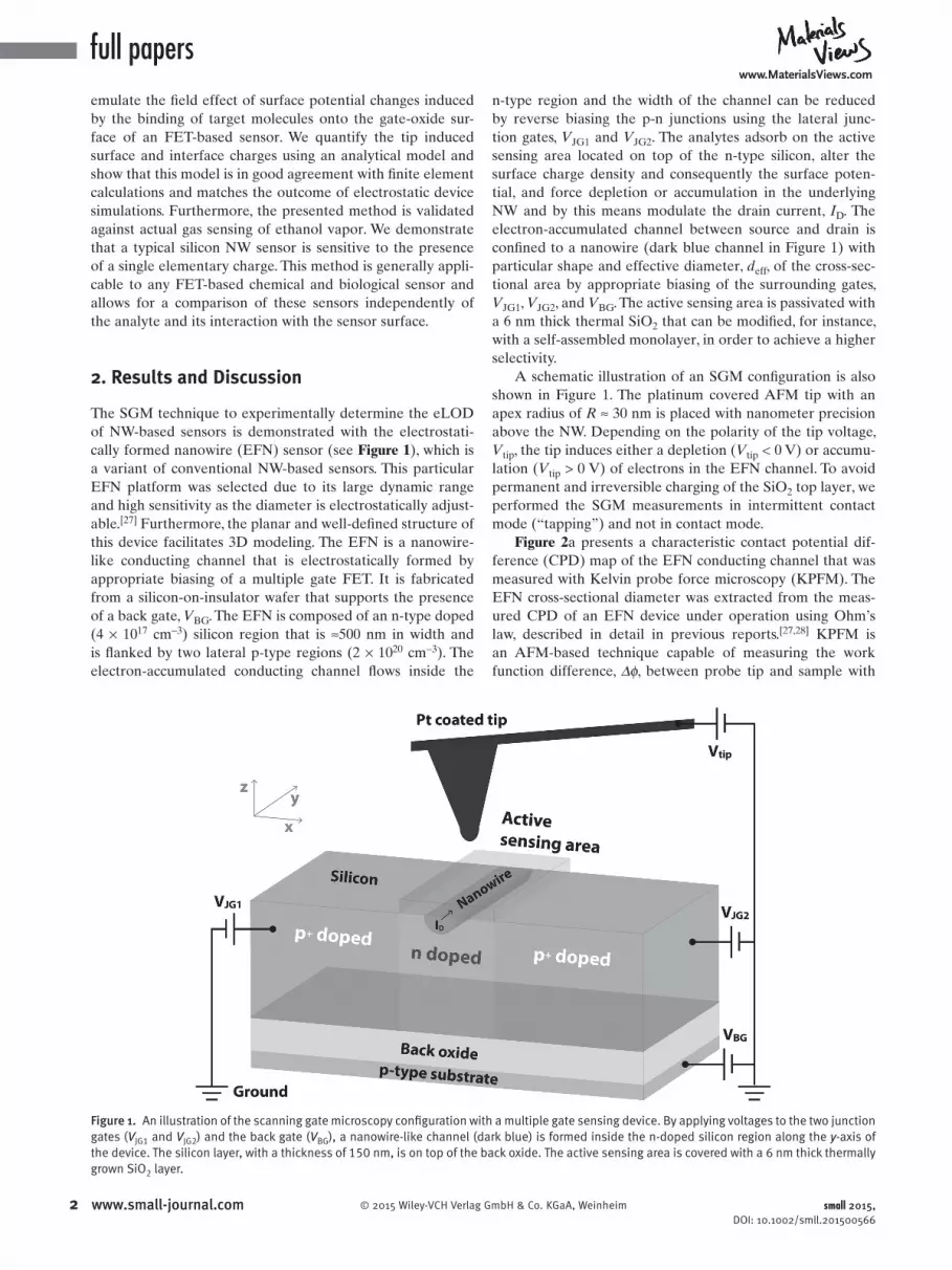
The SGM technique to experimentally determine the eLOD
of NW-based sensors is demonstrated with the electrostati-
cally formed nanowire (EFN) sensor (see Figure 1 ), which is
a variant of conventional NW-based sensors. This particular
EFN platform was selected due to its large dynamic range
and high sensitivity as the diameter is electrostatically adjust-
able. [ 27 ] Furthermore, the planar and well-defi ned structure of
this device facilitates 3D modeling. The EFN is a nanowire-
like conducting channel that is electrostatically formed by
appropriate biasing of a multiple gate FET. It is fabricated
from a silicon-on-insulator wafer that supports the presence
of a back gate, V BG . The EFN is composed of an n-type doped
(4 × 10 17 cm −3 ) silicon region that is ≈500 nm in width and
is fl anked by two lateral p-type regions (2 × 10 20 cm −3 ). The
electron-accumulated conducting channel fl ows inside the
n-type region and the width of the channel can be reduced
by reverse biasing the p-n junctions using the lateral junc-
tion gates, V JG1 and V JG2 . The analytes adsorb on the active
sensing area located on top of the n-type silicon, alter the
surface charge density and consequently the surface poten-
tial, and force depletion or accumulation in the underlying
NW and by this means modulate the drain current, I D . The
electron-accumulated channel between source and drain is
confi ned to a nanowire (dark blue channel in Figure 1 ) with
particular shape and effective diameter, d eff , of the cross-sec-
tional area by appropriate biasing of the surrounding gates,
V JG1 , V JG2 , and V BG . The active sensing area is passivated with
a 6 nm thick thermal SiO 2 that can be modifi ed, for instance,
with a self-assembled monolayer, in order to achieve a higher
selectivity.
A schematic illustration of an SGM confi guration is also
shown in Figure 1 . The platinum covered AFM tip with an
apex radius of R ≈ 30 nm is placed with nanometer precision
above the NW. Depending on the polarity of the tip voltage,
V tip , the tip induces either a depletion ( V tip < 0 V) or accumu-
lation ( V tip > 0 V) of electrons in the EFN channel. To avoid
permanent and irreversible charging of the SiO 2 top layer, we
performed the SGM measurements in intermittent contact
mode (“tapping”) and not in contact mode.
Figure 2 a presents a characteristic contact potential dif-
ference (CPD) map of the EFN conducting channel that was
measured with Kelvin probe force microscopy (KPFM). The
EFN cross-sectional diameter was extracted from the meas-
ured CPD of an EFN device under operation using Ohm’s
law, described in detail in previous reports. [ 27,28 ] KPFM is
an AFM-based technique capable of measuring the work
function difference, Δ φ, between probe tip and sample with
small 2015, DOI: 10.1002/smll.201500566
Figure 1. An illustration of the scanning gate microscopy confi guration with a multiple gate sensing device. By applying voltages to the two junction gates ( V JG1 and V JG2 ) and the back gate ( V BG ), a nanowire-like channel (dark blue) is formed inside the n-doped silicon region along the y -axis of the device. The silicon layer, with a thickness of 150 nm, is on top of the back oxide. The active sensing area is covered with a 6 nm thick thermally grown SiO 2 layer.

www.MaterialsViews.com
3© 2015 Wiley-VCH Verlag GmbH & Co. KGaA, Weinheim www.small-journal.com
nanometer spatial resolution and meV sensitivity. [ 29, 30 ] It was
found that the effective NW diameter is tunable in a range
from 115 to 22 nm by reducing the two junction gate biases,
V JG12 , from 0 to −2 V. Note that the CPD image in Figure 2 a
resolves the p-doped regions (red) and the n-doped channel
(blue) through the SiO 2 top layer. Figure 2 b shows SGM
measurements where the drain current was measured as a
function of the tip position (indicated by dashed arrows in
Figure 2 a) at V tip = −1 V for an effective channel diameter of
115 nm ( V JG12 = 0 V). The tip has the strongest effect (local
depletion) on I D when it is placed in the lateral and trans-
versal center of the NW. Local variations on a sensor surface,
e.g., in NW-based bio(chemical) sensors where an optimal
placement of receptors is important to achieve a high sensi-
tivity, [ 26 ] can be identifi ed due to the high precision of the tip
gate positioning.
Figure 3 a shows CPD images of the EFN sensing
area under device operation before and after exposure
to ≈2000 ppm of ethanol, and demonstrates the “molec-
ular” gating effect of the adsorbed ethanol on the EFN.
The adsorbed ethanol molecules induce a CPD (= −surface
potential) shift of ≈50 mV in the p-type region and lead to
an overall CPD increase of ≈180 mV in the n-doped EFN
channel region, as shown in the CPD profi les along the
p-n-p region in Figure 3 b. This positive CPD change is a
direct evidence that the surface is negatively charged upon
ethanol adsorption due to surface polarization, in agreement
with previous work. [ 31 ] This negatively charged layer acts as
a molecular gate causing depletion in the n-doped region
and resulting in a more positive CPD (more p-type) of the
nanowire. The highly complex interaction of ethanol with an
SiO 2 surface was studied in previous works, e.g., by Chang
and Shu. [ 32 ] KPFM measurements are supported by I D – V D
characteristics of the EFN device (Figure 3 c) showing the
decrease in I D following ethanol adsorption.
The complete EFN device was simulated with a 3D
device simulator (Synopsys TCAD Sentaurus, Mountain
View, USA) taking into account the actual process
parameters, where for each mesh point the Poisson and con-
tinuity equations were numerically solved. Figure 4 a shows
a semilogarithmic plot of the measured I D (red squares)
as a function of the applied tip voltage, V tip , and the simu-
lated I D (black triangles) as a function of the fi xed charge
inside a 10 3 nm 3 SiO 2 cube placed on top and in the center
small 2015, DOI: 10.1002/smll.201500566
Figure 2. a) Contact potential difference (CPD) image of an EFN under operation for V D = 1 V and V JG12 = 0 V. The dashed arrows indicate the scanning lines across the p-n-p junction in scanning gate microscopy. b) The 3D plot shows the drain current as a function of the tip position on the X - and Y -axis for V tip = −1 V. The tip–sample distance, δ , was kept constant at ≈15 nm.
Figure 3. a) CPD images of the EFN active area before and after ethanol exposure (≈2000 ppm) under device operation at V D = 1 V and V JG12 = −0.5 V. b) CPD line profi les, indicated by dashed arrows in (a), across the p-n-p junction of the EFN before and after ethanol adsorption. Ethanol alters the surface potential causing a depletion of the conductive channel in the n-doped region refl ected in the more positive CPD compared with the bare EFN. c) The corresponding I D – V D characteristics show a decrease in I D by a factor of ≈2 following ethanol exposure.

full paperswww.MaterialsViews.com
4 www.small-journal.com © 2015 Wiley-VCH Verlag GmbH & Co. KGaA, Weinheim
of the active sensing area. The measurements and simula-
tions were performed for two NW diameters with distinct
sensitivity and large dynamic range, d eff of 80 and 30 nm by
applying V JG12 = −0.5 V and V JG12 = −1.5 V, respectively. The
measured I D – V tip curves are reminiscent of the transfer
characteristics, I D – V G , of a conventional FET, which can
be switched on and off by appropriate biasing of the gate
voltage, V G . The simulations are in accordance with the
measured I D – V tip characteristics: A negative (positive) tip
voltage is equivalent to a negative (positive) charge placed
on top of the sensor, which closes (opens) the channel
(EFN). It is evident from the plot in Figure 4 a that the effect
of the tip gate on the drain current, expressed in terms of
sensitivity, S = ΔI D / I D , is greater for smaller d eff . For instance,
we obtain a higher sensitivity, S 30 nm = 0.27 > S 80 nm = 0.1, for
the NW with d eff = 30 nm than for the NW with d eff = 80 nm
( V tip = −1 V) although the active area is larger for the latter
providing more binding sites. This result is refl ected in the
higher on/off ratio (10 2 –10 3 ) of the 80 nm wide EFN com-
pared with the lower on/off ratio (<10) of the 30 nm narrow
EFN. This fundamental result is in agreement with ethanol
gas sensing experiments (Figure 4 b), where the EFN sensor
was exposed to ethanol concentrations in the range of
10–2000 ppm for NWs with diameters of 80 and 30 nm at
a negative V BG . The increase in sensitivity with decreasing
d eff is explained by the infl uence of the local electric fi eld
that stems from a change in the surface charge density
due to adsorbed analyte (ethanol here) or the tip on the
electron density distribution inside the NW; smaller NW
is more affected by a local electrostatic fi eld. The Debye
screening length was calculated for the n-doped silicon with
the expression, DB
2d
L k Tq Nε= , for semiconductors where k B
is the Boltzmann constant, T is the temperature, ε is the die-
lectric constant, and N d is the donor density of the n-type
region, resulting in L D ≈ 6. Therefore, induced surface
charges are partially screened. The tip gate measurements
can predict the lower limit of a minimum detectable surface
charge and are in qualitative agreement with ethanol gas
sensing experiments. However, for a quantitative comparison
the tip induced surface charge has to be translated into
an analyte concentration. This requires information on the
interaction of the analyte with the surface, in particular the
binding equilibrium kinetics and surface coverage.
We have calculated the tip induced surface and interface
charges for the probe geometry shown in Figure 5 adapting
the general analytical solution for the electrostatic fi eld of
a point charge, Q , in a three-dielectric medium derived by
Barrera et al. [ 33 ] using the method of images. Instead of a
point charge, we considered the electrostatic fi eld and sur-
face charge density of an AFM tip. The detailed calculation
is provided in the Supporting Information. For tip–sample
distances in the range of (or larger than) the apex radius, the
contribution of the cone becomes signifi cant. [ 34–36 ] As illus-
trated in Figure 5 , the tip is modeled as a truncated cone with
a semispherical tip apex of radius R at a tip–sample distance
small 2015, DOI: 10.1002/smll.201500566
Figure 4. a) The tip voltage is shown as function of the measured drain current, I D , for two different channel diameters, 80 and 30 nm, in a semilogarithmic plot, and compared with the simulated I D plotted as a function of the fi xed charge placed above the NW center. The applied tip voltage, V tip , was swept from −10 to 10 V at a fi xed tip position ( δ ≈ 15 nm) above the active sensing area. V D = 1 V and V BG = 0 V. b) I D is plotted as a function of the ethanol vapor concentration that was varied from 10 to 2000 ppm, at V D = 1 V and V BG = −3 V in a sensing experiment for two different channel diameters, 80 and 30 nm.
Figure 5. A schematic representation of the tip above the sample surface showing the dimensions and parameters used in the analytical model that was solved to quantify the tip induced surface and interface charges, q 32 and q 21 , respectively. L , r , and θ are the cone length, radius, and half-cone angle, respectively. σ cone and σ apex are the surface charge densities of tip cone and apex, respectively. The tip apex with radius R is located in a medium with dielectric constant ε 3 (nitrogen) at a tip–sample distance δ . The surface top layer with thickness t and dielectric constant ε 2 (SiO 2 ) covers the bulk material with dielectric constant ε 1 (silicon).
www.MaterialsViews.com
5© 2015 Wiley-VCH Verlag GmbH & Co. KGaA, Weinheim www.small-journal.com
δ . [ 34 ] Terris et al. [ 37 ] investigated the charging of an oxidized
Si surface using AFM and suggested a spherical model for
the tip, where the capacitance is modeled by a sphere above
a conductive plane, 4apex 01
1
C Rsinh sinhnn∑πε α α( )= −
=
∞, where
11cosh Rα δ( )= +− . The electric fi eld of the cone is approxi-
mated by the fi eld generated by a charge line of constant
charge density, 411cone 0 tip
1
V ln coscosλ πε θ
θ{ }( )≈ +−
−, suggested by
Hao et al. [ 38 ] The tip induced surface charge densities were
obtained expanding the solution of Barrera et al. [ 33 ] using the
expression for the tip apex charge, Q apex = V tip C apex , and infi n-
itesimal cone charge, dd
11
conetip
1Qs V ln cos
cosθθ{ }( )= +
−
−, where s
is the distance to the center of curvature of the apex. The
total fi eld of the tip and consequently the total induced sur-
face and interface charge density is the sum of conical and
spherical contributions, tot ap coij ij ijσ ρ σ ρ σ ρ( ) ( ) ( )= + , where
ρ is the radial coordinate in a cylindrical coordinate system
with azimuthal symmetry and ij = 32 and ij = 21 indicate the
surface and interface plane, respectively. The total charge
(at V tip = 1 V) induced on the entire (infi nite) surface and
interface planes, q 32 and q 21 , respectively, is obtained by
solving the integral equation of the respective charge densi-
ties, σ ij , for an infi nite plane
2 d
0
q ij ij∫ρ π ρσ ρ ρ( ) ( )=∞
(1)
Each tip voltage corresponds to a specifi c charge quantity,
which is simply obtained by multiplying q ij ( ρ ) with V tip due its
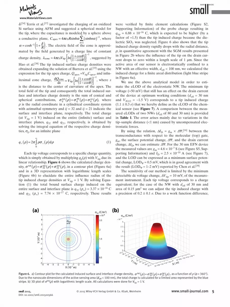
linear relationship. Figure 6 shows the calculated charge den-
sity, tot32tot
21totσ ρ σ ρ σ ρ( ) ( ) ( )= + , in a contour plot (Figure 6 a)
and in a 3D representation with logarithmic length scales
(Figure 6 b) to elucidate the entire infl uence radius of the
tip induced charge densities at V tip = 1 V. By solving Equa-
tion ( 1) the total bound surface charge induced on the
entire surface and interface plane is q 32 ( ρ ∞ ) = 3.37 × 10 −16 C
and q 21 ( ρ ∞ ) = 7.74 × 10 −17 C, respectively. These results
were verifi ed by fi nite element calculations (Figure S2,
Supporting Information) of the probe charge resulting in
q tip = 6.88 × 10 −16 C, which is expected to be higher (by a
factor of ≈1.5) than the tip induced charge because the die-
lectric SiO 2 was neglected. Figure 6 also shows that the tip
induced charge density rapidly drops with the radial distance,
ρ , in quantitative agreement with the SGM results presented
in Figure 2 b where the infl uence of the tip on the drain cur-
rent drops to zero within a length scale of 1 µm. Since the
active area of our sensor is electrostatically confi ned to a
NW with an effective width, d eff < 100 nm, we calculated the
induced charge for a fi nite areal distribution (light blue stripe
in Figure 6 a).
We use the above analytical model in order to esti-
mate the eLOD of the electrostatic NW. The minimum tip
voltage (≈50 mV) that still has an effect on the drain current
of the device at optimum working conditions ( d eff = 30 nm
and V JG12 = −1.5 V) corresponds to a tip induced charge
(1.1 ± 0.3 e ) that we hereby defi ne as the eLOD of the chem-
ical sensor (see Figure 7 ). A comparison between the meas-
ured eLODs of two NWs ( d eff of 80 and 30 nm) is provided
in Table 1 . The error arises mainly due to variations in the
tip–sample distance (<1 nm) caused by uncompensated elec-
trostatic forces.
By using the relation, ΔI D = g m × Δ Ψ, [ 16 ] between the
transconductance with respect to the molecular (top) gate,
g m , the surface potential change, Δ Ψ, and the drain current
change, ΔI D , we can estimate Δ Ψ. For the 30 nm EFN device
the measured values are g m = 4.6 × 10 −7 S (see Figure S5, Sup-
porting Information) and I D = 2.5 × 10 −10 A (see Figure 7 ),
and the LOD can be expressed as a minimum surface poten-
tial change, LOD Ψ ≈ 0.5 mV, which is in good agreement with
the result (LOD Ψ ≈ 1–2 mV) reported by Chen et al. [ 39 ]
The sensitivity of our method is limited by the minimum
detectable dc voltage change, ΔV tip = 10 mV, of the measure-
ment instrument. Each tip voltage corresponds to a charge
equivalent; for the case of the NW with d eff of 30 nm and
area of 0.15 µm 2 we can adjust the tip induced charge with
a precision of 0.2 ± 0.1 e . Due to a work function difference,
small 2015, DOI: 10.1002/smll.201500566
Figure 6. a) Contour plot for the calculated induced surface and interface charge density, tot32tot
21totσ ρ σ ρ σ ρ( ) ( ) ( )= + , as a function of ρ ( φ = 360°).
Due to the nanoscale dimensions of the active sensing area ( d eff < 100 nm), the total charge is calculated for a limited area represented by the blue stripe. b) 3D plot of σ tot ( ρ ) with logarithmic length scale. All calculations were done for V tip = 1 V.

full paperswww.MaterialsViews.com
6 www.small-journal.com © 2015 Wiley-VCH Verlag GmbH & Co. KGaA, Weinheim
Δ φ, between tip and sample, there is an additional charge
contribution to the total charge, ts tipq r C r V eφ( ) ( )= − Δ⎛
⎝⎜⎞⎠⎟ ,
where C ts is the tip–sample capacitance. The tip induced
charges are compensated by applying a tip voltage, V tip = Δ φ/ e .
Concurrently, at V tip = 0 V, the tip induced surface charges are
not zero but are given by Δ φ. For the measured Δ φ of ≈70 mV
using KPFM (Figure 2 a) the tip induced surface charge
corresponds to 1.2 ± 0.3 e for the small NW at V tip = 0 V.
Acceptor-like surface and interface states, negatively charged
if occupied, are known to be present in silicon with a con-
centration of ≈1 × 10 11 cm 2 . [ 40 ] However, surface states are
an inherent part of any chemical sensor and screen external
electric fi elds Therefore, the measured eLOD is even lower
if taking into account surface states. In the electrostatic
simulations surface states and also ambient atmosphere
(humidity) were neglected. This explains the larger effect (by
a factor of ≈6) of a specifi c charge quantity on the simulated
I D compared with the measured I D in the tip gate experiment
(see Figure 4 a).
3. Conclusion
We have introduced a method to measure the electrostatic
LOD of NW FET-based sensors using scanning gate micros-
copy and analytical modeling. The AFM tip is used as a local
gate to emulate the fi eld effect of a molecular gate where ana-
lytes adsorb and induce a surface potential change. We have
demonstrated that the electrostatically formed nanowire-
based chemical sensor can potentially achieve an eLOD of a
single elementary charge.
4. Experimental Section
Scanning Gate Microscopy and Kelvin Probe Force Micros-copy : SGM was carried out with a commercial AFM (Dimension Edge, Bruker) inside a nitrogen glove box with less than 1 ppm H 2 O. Highly conductive cantilevers with Pt/Ir coating (PPP EFM, Nanosensors) were used for both SGM and KPFM. In order to minimize the height error of the AFM tip (<1 nm) due to uncom-pensated electrostatic forces, [ 41–43 ] which increase as a function of V tip , the measurements with a free vibration amplitude, A 0 , of below 15 nm were performed and a relatively low amplitude set point, A sp ≤ 5 nm, for the feedback loop that controls the tip–sample distance was used. [ 43 ] The CPD was measured simultane-ously with the topographic signal using amplitude modulation KPFM at an effective tip sample distance of 5–10 nm during scan-ning. The topographic height was obtained by maintaining the amplitude of the fi rst cantilever resonance ( f 1st ≈ 75 kHz) at a pre-defi ned amplitude set point of ≈5 nm. The CPD was determined by compensating the ac component of the electrostatic force, F ES , at angular frequency ω with an applied dc voltage (= |CPD|) in a feedback control loop. To separate topographic from CPD signal, increase the sensitivity, and minimizing probe convolution effects, the ac electrostatic force component was generated at the second resonance, [ 44,45 ] f 2nd ≈ 450 kHz, of the cantilever by applying an ac voltage of about 500 mV. The CPD of the EFN sensing area was measured before and after exposure to ≈2000 ppm of ethanol vapor in order to demonstrate the molecular gating effect. For this purpose ethanol vapor was introduced inside the glove box while the EFN device was operated and the drain current measured simultaneously.
EFN Device Fabrication : The EFN transistors were fabricated by a semiconductor foundry (TowerJazz, Migdal Haemek, Israel) in a conventional and low-cost CMOS process with four masks to implant the different dopant regions for the channel, source–drain and junction gate contacts. The actual doping densities, blanket Arsenic of 4 × 10 17 cm −3 , junction gate Boron of 2 × 10 20 cm −3 , and source–drain Arsenic of 7 × 10 19 cm −3 , were determined post-fabrication by time-of-fl ight secondary ion mass spectrometry (TOF-SIMS). The measured doping density depth profi les served as input for 3D electrostatic simulations. Boron doped 8 in. SOI wafers with an initial doping density of 1.5 × 10 14 cm 2 and a thick-ness of 150 nm were used. The thickness of the buried SiO 2 was 1.5 µm. The thermal SiO 2 gate dielectric was formed at 1200 °C. The critical dimension (lowest spatial limit) of the process was (540 ± 20) nm, defi ned by the spacing between the two p-doped regions (junctions) in the active area of the sensor. The wafer was diced to 1 cm 2 squares and Ti/Au contacts were manufactured by optical lithography and subsequent metal evaporation.
Electrical Characterization and Gas Sensing : Current–voltage characteristics as a function of drain electrode bias ( I D – V D ), back gate electrode bias ( I D – V BG ), and junction gate electrodes ( I D – V JG12 ), were performed using a semiconductor parameters ana-lyzer (B1500A, Agilent). Sensing of ethanol vapor was done in a
small 2015, DOI: 10.1002/smll.201500566
Figure 7. Drain current plotted as a function of time for different tip voltages and a fi xed tip position above the nanowire-like conductive channel for d eff = 30 nm ( V JG12 = −1.5 V). The graph shows the minimum detectable tip voltage expressed in terms of a charge equivalent (= eLOD) obtained from the analytical calculations. V D = 1 V and V BG = 0 V.
Table 1. Comparison of measured detection limits between electrostatic NWs with two different diameters, d eff of 80 and 30 nm, respectively. S e denotes the electrostatic sensitivity.
d eff [nm]
V tip min [mV]
ΔI D [ e −1 ]
S e [ e −1 ]
LOD Ψ [mV]
eLOD [e]
80 60 2.5 × 10 −10 0.01 0.9 2.3 ± 0.4
30 50 1.25 × 10 −9 0.02 0.5 1.1 ± 0.3

www.MaterialsViews.com
7© 2015 Wiley-VCH Verlag GmbH & Co. KGaA, Weinheim www.small-journal.comsmall 2015, DOI: 10.1002/smll.201500566
controlled N 2 (99.999% purity) atmosphere in a sealed metallic gas chamber connected to a gas dilution system. Ethanol gas was generated in a bubbler system and diluted with N 2 and mass fl ow controllers. A reference sensor (ppbRAE 3000, RAE Systems) was connected to the gas chamber in order to monitor the analyte con-centration inside the chamber down to 100 ppb level.
Supporting Information
Supporting Information is available from the Wiley Online Library or from the author.
Acknowledgements
A.H. acknowledges the support of the Tel Aviv University Center for Nanoscience and Nanotechnology.
[1] Y. Cui , Q. Wei , H. Park , C. M. Lieber , Science 2001 , 293 , 1289 . [2] D. Zhang , Z. Liu , C. Li , T. Tang , X. Liu , S. Han , B. Lei , C. Zhou , Nano
Lett. 2004 , 4 , 1919 . [3] G. Zheng , F. Patolsky , Y. Cui , W. U. Wang , C. M. Lieber , Nat. Bio-
technol. 2005 , 23 , 1294 . [4] M. C. McAlpine , H. Ahmad , D. Wang , J. R. Heath , Nat. Mater. 2007 ,
6 , 379 . [5] a) Y. Engel , R. Elnathan , A. Pevzner , G. Davidi , E. Flaxer ,
F. Patolsky , Angew. Chem. 2010 , 122 , 6982 ; b) Y. Engel , R. Elnathan , A. Pevzner , G. Davidi , E. Flaxer , F. Patolsky , Angew. Chem. Int. Ed. 2010 , 49 , 6830 .
[6] A. Cao , E. J. R. Sudhölter , L. C. P. M. de Smet , Sensors 2014 , 14 , 245 .
[7] Y. Paska , T. Stelzner , S. Christiansen , H. Haick , ACS Nano 2011 , 5 , 5620 .
[8] Y. Paska , T. Stelzner , O. Assad , U. Tisch , S. Christiansen , H. Haick , ACS Nano 2012 , 6 , 335 .
[9] B. Wang , H. Haick , ACS Appl. Mater. Interfaces 2013 , 5 , 2289 . [10] B. Wang , J. C. Cancilla , J. S. Torrecilla , H. Haick , Nano Lett. 2014 ,
14 , 933 . [11] X. Zhao , B. Cai , Q. Tang , Y. Tong , Y. Liu , Sensors 2014 , 14 ,
13999 . [12] J. Kong , N. R. Franklin , C. Zhou , M. G. Chapline , S. Peng , K. Cho ,
H. Dai , Science 2000 , 287 , 622 . [13] P. G. Collins , K. Bradley , M. Ishigami , A. Zettl , Science 2000 , 287 ,
1801 . [14] J. Li , Y. Lu , Q. Ye , M. Cinke , J. Han , M. Meyyappan , Nano Lett.
2003 , 3 , 929 . [15] G. Shalev , G. Landman , I. Amit , Y. Rosenwaks , I. Levy , NPG Asia
Mater. 2013 , 5 , e41 . [16] N. K. Rajan , X. Duan , M. A. Reed , Wiley Interdiscip. Rev.: Nanomed.
Nanobiotechnol. 2013 , 5 , 629 .
[17] D. MacDougall , W. B. Crummett , Anal. Chem. 1980 , 52 , 2242 . [18] L. A. Currie , Anal. Chim. Acta 1999 , 391 , 127 . [19] P. R. Nair , M. A. Alam , Appl. Phys. Lett. 2006 , 88 , 233120 . [20] K. Seshadri , C. D. Frisbie , Appl. Phys. Lett. 2001 , 78 , 993 . [21] R. Jalilian , L. A. Jauregui , G. Lopez , J. Tian , C. Roecker ,
M. M. Yazdanpanah , R. W. Cohn , I. Jovanovic , Y. P. Chen , Nano-technology 2011 , 22 , 295705 .
[22] A. Bachtold , M. S. Fuhrer , S. Plyasunov , M. Forero , E. H. Anderson , A. Zettl , P. L. McEuen , Phys. Rev. Lett. 2000 , 84 , 6082 .
[23] M. Freitag , A. T. Johnson , S. V. Kalinin , D. A. Bonnell , Phys. Rev. Lett. 2002 , 89 , 216801 .
[24] M. T. Woodside , P. L. McEuen , Science 2002 , 296 , 1098 . [25] X. Zhou , S. A. Dayeh , D. Wang , E. T. Yu , Appl. Phys. Lett. 2007 , 90 ,
233118 . [26] D. Martin , A. Heinzig , M. Grube , L. Geelhaar , T. Mikolajick ,
H. Riechert , W. M. Weber , Phys. Rev. Lett. 2011 , 107 , 216807 . [27] A. Henning , N. Swaminathan , A. Godkin , G. Shalev ,
I. Amit , Y. Rosenwaks , Nano Res. 2015 , DOI: 10.1007/s12274-015-0729-7 .
[28] E. Koren , Y. Rosenwaks , J. E. Allen , E. R. Hemesath , L. J. Lauhon , Appl. Phys. Lett. 2009 , 95 , 092105 .
[29] M. Nonnenmacher , M. P. O’Boyle , H. K. Wickramasinghe , Appl. Phys. Lett. 1991 , 58 , 2921 .
[30] T. Glatzel , in Springer Series in Surface Sciences , Vol. 48 (Eds: S. Sadewasser , T. Glatzel ), Springer , Berlin, Germany 2011 , Ch. 13 .
[31] E. Atanassova , T. Dimitrova , Solid-State Electron. 1993 , 36 , 1711 . [32] C.-C. Chang , M.-C. Shu , J. Phys. Chem. B 2003 , 107 , 7076 . [33] R. G. Barrera , O. Guzmán , B. Balaguer , Am. J. Phys. 1978 , 46 , 1172 . [34] S. Hudlet , M. Saint Jean , C. Guthmann , J. Berger , Eur. Phys. J. B
1998 , 2 , 5 . [35] M. Saint Jean , S. Hudlet , C. Guthmann , J. Berger , J. Appl. Phys.
1999 , 86 , 5245 . [36] G. Cohen , E. Halpern , S. U. Nanayakkara , J. M. Luther , C. Held ,
R. Bennewitz , A. Boag , Y. Rosenwaks , Nanotechnology 2013 , 24 , 295702 .
[37] B. D. Terris , J. E. Stern , D. Rugar , H. J. Mamin , Phys. Rev. Lett. 1989 , 63 , 2669 .
[38] H. W. Hao , A. M. Baró , J. J. Sáenz , J. Vac. Sci. Technol., B: Micro-electron. Nanometer Struct.–Process., Meas., Phenom. 1991 , 9 , 1323 .
[39] S. Chen , A. van den Berg , E. T. Carlen , Sens. Actuators, B 2015 , 209 , 486 .
[40] A. S. Grove , B. E. Deal , E. H. Snow , C. T. Sah , Solid-State Electron. 1965 , 8 , 145 .
[41] S. Sadewasser , P. Carl , T. Glatzel , M. C. Lux-Steiner , Nanotech-nology 2004 , 15 , S14 .
[42] S. Sadewasser , M. C. Lux-Steiner , Phys. Rev. Lett. 2003 , 91 , 266101 .
[43] D. Ziegler , J. Rychen , N. Naujoks , A. Stemmer , Nanotechnology 2007 , 18 , 225505 .
[44] A. Kikukawa , S. Hosaka , R. Imura , Appl. Phys. Lett. 1995 , 66 , 3510 .
[45] T. Glatzel , S. Sadewasser , M. C. Lux-Steiner , Appl. Surf. Sci. 2003 , 210 , 84 .
Received: February 26, 2015 Revised: May 28, 2015Published online:


