Embed Size (px)
Citation preview

Nano Res. 2011, 4(3): 259–265
259
Hot-Electron Effects in InAs Nanowire Josephson Junctions
Stefano Roddaro1 ( ), Andrea Pescaglini1, Daniele Ercolani1, Lucia Sorba1, Francesco Giazotto1 ( ), and
Fabio Beltram1, 2 1 NEST, Istituto Nanoscienze-CNR and Scuola Normale Superiore, P. za S. Silvestro 12, I-56127 Pisa, Italy 2 IIT@NEST, Center for Nanotechnology Innovation, P. za S. Silvestro 12, I-56127 Pisa, Italy Received: 1 October 2010 / Revised: 8 November 2010 / Accepted: 8 November 2010 © Tsinghua University Press and Springer-Verlag Berlin Heidelberg 2010
ABSTRACT The controlled tailoring of the energy distribution in an electron system opens the way to interesting new physics and device concepts, as demonstrated by research on metallic nanodevices during recent years. Here we investigate how Josephson coupling in a superconductor–InAs nanowire junction can be tuned by means of hot-electron injection and we show that a complete suppression of superconductive effects can be achieved using a power as low as 100 pW. Nanowires offer a novel design freedom as they allow axial and radial heterostructures to be defined as well as control over doping profiles, which can be crucial in the development of devices—such as nanorefrigerators—where precisely controlled and predictable energy barriers are mandatory. Our work provides estimates for unknown key thermal and electrical parameters, such as the electron–phonon coupling, in our InAs nanostructures. KEYWORDS Nanowire, hot-electron, Josephson effect, InAs, heat conduction
1. Introduction
A transparent interface between a superconductor (S) and a normal metal (N) can be used to induce, in the neighborhood of the junction, pairing correlations in the N region. This so-called “proximity effect” [1–3] strongly modifies the transport properties of the electron system and can lead to a supercurrent flow in SNS junctions [4]. Recent experimental work has shown the potential of semiconductor nanowires (NWs) as building blocks for different types of nanoscale devices [5–8]. In the case of hybrid systems, supercurrent flow was observed in NW devices containing superconducting contacts and both field- effect [9–11] and single-electron [12, 13] control of the
Josephson effect has been successfully demonstrated. Here, we investigate Josephson junctions based on InAs NWs and show that the supercurrent can be efficiently controlled by hot quasiparticle injection from non-superconducting electrodes. The device operation principle is based on the modification of the energy distribution of the NW electron system: this allows one to tune the Josephson current [14–16], invert the sign of its phase–current relation [17–19] and even enhance superconductive effects [19–21]. This is known to afford high-switching speeds in metallic systems [15]. We shall argue that in the context of semiconductor NWs this opens the way to perspectives for novel implementation of device concepts based on hybrid superconductor–normal metal systems [22].
Nano Res. 2011, 4(3): 259–265 ISSN 1998-0124DOI 10.1007/s12274-010-0077-6 CN 11-5974/O4Research Article
Address correspondence to Stefano Roddaro, [email protected]; Francesco Giazotto, [email protected]

Nano Res. 2011, 4(3): 259–265
260
2. InAs Josephson junctions
One practical implementation of our InAs-NW hot- electron Josephson devices is shown in Fig. 1(a). The SNS junction was fabricated by e-beam lithography starting from an n-doped InAs NW (the N region, see the Electronic Supplementary Material (ESM) for further NW characteristics). The junction is formed by two Ti/Al superconducting electrodes placed at a distance L ~ 60 nm (S regions) on top of the NW. Control electrodes were fabricated by depositing two additional normal metal Ti/Au leads at the two ends
Figure 1 Hot-electron Josephson junctions. (a) Scanning electron micrograph of one of the measured devices: an InAs NW is coupled to two 250 nm-wide Ti/Al electrodes (green) to form a Josephson junction which is about 60 nm long. The InAs NW is also contacted at its ends to two normal metal Ti/Au leads (yellow) which are used to control the electron energy distribution in the junction through quasiparticle injection. The supercurrent IJ can thus be tuned by voltage biasing the N control line with Vinj. The distance between the two normal metal electrodes is Linj ~ 1 μm. The overlaid schematic shows a sketch of the measurement set-up: supercurrent is detected using a four-wire scheme, while the injection circuit consists of a floating network. (b) Schematic cross-section view of a typical device with relevant geometrical details. Devices were fabricated on top of an insulating Si/SiO2 substrate by electron-beam lithography and metal deposition
of the NW. As schematically illustrated by the overlay of Fig. 1(a), the N leads are used to drive a dissipative current through the NW thereby tuning Josephson coupling in the S–NW–S structure.
Figure 2(a) shows a set of typical Ⅳ characteristics from one of the measured S–NW–S junctions at equilibrium (i.e., Vinj = 0) and at different bath tem- peratures T. High critical currents up to Ic ~ 350 nA (corresponding to a supercurrent density of approxi- mately 5.5 kA/cm2) are observed and Josephson
Figure 2 Temperature dependence of the Josephson current. (a) The Ⅳ characteristics IJ vs. VJ of device D2 demonstrate the presence of dissipationless transport up to a temperature T ~ 1 K. Ic is the critical current of the junction, and the hatched area provides a guide to the eye to emphasize the supercurrent suppression as a function of temperature. The curves are horizontally shifted for clarity. (b) Evolution of the measured equilibrium critical current Ic as a function of bath temperature T for two representative devices (D1—red circles, D2—blue triangles). The dashed line is the theoretical prediction for an ideal short diffusive SNS junction. The junction resistance in the normal state is RN ~ 220 Ω and ~210 Ω for device D1 and D2, respectively
Nano Res. 2011, 4(3): 259–265
261
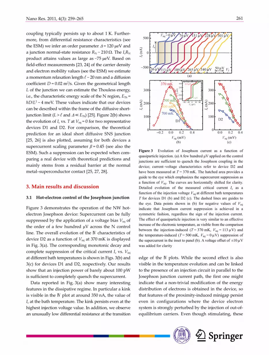
coupling typically persists up to about 1 K. Further- more, from differential resistance characteristics (see the ESM) we infer an order parameter Δ = 120 μeV and a junction normal-state resistance RN ~ 210 Ω. The IcRN product attains values as large as ~75 μeV. Based on field-effect measurements [23, 24] of the carrier density and electron mobility values (see the ESM) we estimate a momentum relaxation length ℓ ~ 20 nm and a diffusion coefficient D = 0.02 m2/s. Given the geometrical length L of the junction we can estimate the Thouless energy, i.e., the characteristic energy scale of the N region, ETh = ħD/L2 ~ 4 meV. These values indicate that our devices can be described within the frame of the diffusive short- junction limit (L > ℓ and Δ << ETh) [25]. Figure 2(b) shows the evolution of Ic vs. T at Vinj = 0 for two representative devices D1 and D2. For comparison, the theoretical prediction for an ideal short diffusive SNS junction [25, 26] is also plotted, assuming for both devices a supercurrent scaling parameter β = 0.45 (see also the ESM). Such a suppression can be expected when com- paring a real device with theoretical predictions and mainly stems from a residual barrier at the normal metal–superconductor contact [25, 27, 28].
3. Main results and discussion
3.1 Hot-electron control of the Josephson junction
Figure 3 demonstrates the operation of the NW hot- electron Josephson device: Supercurrent can be fully suppressed by the application of a voltage bias Vinj of the order of a few hundred μV across the N control line. The overall evolution of the Ⅳ characteristics of device D2 as a function of Vinj at 370 mK is displayed in Fig. 3(a). The corresponding monotonic decay and complete suppression of the critical current Ic vs. Vinj at different bath temperatures is shown in Figs. 3(b) and 3(c) for devices D1 and D2, respectively. Our results show that an injection power of barely about 100 pW is sufficient to completely quench the supercurrent.
Data reported in Fig. 3(a) show many interesting features in the dissipative regime. In particular a kink is visible in the Ⅳ plot at around 350 nA, the value of Ic at the bath temperature. The kink persists even at the highest injection voltage value. In addition, we observe an unusually low differential resistance at the transition
Figure 3 Evolution of Josephson current as a function of quasiparticle injection. (a) A few hundred μV applied on the control junctions are sufficient to quench the Josephson coupling in the device; current–voltage characteristics refer to device D2 and have been measured at T = 370 mK. The hatched area provides a guide to the eye which emphasizes the supercurrent suppression as a function of Vinj. The curves are horizontally shifted for clarity. Detailed evolution of the measured critical current Ic as a function of the injection voltage Vinj at different bath temperatures T for devices D1 (b) and D2 (c). The dashed lines are guides to the eye. Data points shown in (b) for negative values of Vinj indicate that Josephson current suppression is achieved in a symmetric fashion, regardless the sign of the injection current. The effect of quasiparticle injection is very similar to an effective increase of the electronic temperature, as visible from the comparison between the injection-induced (T = 370 mK, Vinj = 113 μV) and the temperature-induced (T = 500 mK, Vinj = 0 μV) suppression of the supercurrent in the inset to panel (b). A voltage offset of ±10 μV was added for clarity
edge of the Ⅳ plots. While the second effect is also visible in the temperature evolution and can be linked to the presence of an injection circuit in parallel to the Josephson junction current path, the first one might indicate that a non-trivial modification of the energy distribution of electrons is obtained in the device, so that features of the proximity-induced minigap persist even in configurations where the device electron system is strongly perturbed by the injection of out-of- equilibrium carriers. Even though stimulating, these

Nano Res. 2011, 4(3): 259–265
262
experimental features go beyond the scope and the reach of the present investigation. Other technical differences between these devices and comparable implementations are worth discussing but do not lead to qualitatively or quantitatively important effects. In particular, it is worth noting that with respect to previous all-metallic devices [15–17], hot electrons are here injected in the same direction as the Josephson supercurrent flow and in the vicinity of the proxi- mized NW-S interfaces. This is also not expected (nor observed) to affect the device performance.
3.2 Discussion
The device working principle adopted is alternative— in a way complementary—to the well-established successful principle of Josephson field-effect transistors (JoFETs), where supercurrent control is achieved by tuning the charge density in the normal region by electrostatic gating [29, 30]. One advantage of control schemes based on hot electrons is that no electro- statically coupled gate is necessary so that in our device it turns out to be easier to define extremely short SNS junctions with large supercurrent densities, while retaining full tunability of the supercurrent flow. Clearly, such a device approach is amenable to all-metal implementations [15–17]. On the other hand, NW-based architectures offer interesting beneficial features, due to the intrinsic design freedom of semiconductor NWs. In the present device, the higher impedance of the active element leads to a quite low-dissipation device which can be switched by barely applying 100 pW of external power. More generally, the possibility of designing NWs including atomically-precise barriers in the radial/axial direction [7, 23] is also very interesting in view of advanced device schemes based on out-of-equilibrium electron transport such as, for instance, nanorefrigerators [20–22]. In view of these perspectives, in the following we analyze the behavior of our InAs devices in order to extract an estimate of important thermoelectric parameters which can serve as a guide for future device designs.
3.3 Thermal model
Insight into the working principle of this device can be gained by recalling that in diffusive SNS junctions
a continuum spectrum of Andreev bound states is responsible for the supercurrent flow across the struc- ture [14, 25]. Occupation of the supercurrent carrying states is determined by the quasiparticle energy distri- bution in the N region which can, in turn, be controlled through the application of a finite bias Vinj across the NW [14, 25]. While a detailed quantitative description of this effect is rather complex and goes into fine details which are beyond the reach of present experiment, more general and useful considerations can be made. Based on comparable experiments [15], and given the similarity between the evolution reported in Figs. 2(a) and 3(a) (see also the inset to Fig. 3(b)), we argue that the dominant part of the observed effect can be captured in terms of heating of the electron system in the NW, i.e., we make the hypothesis that—upon injection of hot quasiparticles—NW electrons can be described by a quasi-equilibrium Fermi-like energy distribution characterized by a temperature Te larger than the bath temperature [22]. The value Te can be estimated by comparing the Ic suppression as a function of Vinj with the Ic suppression one obtains, in absence of current injection from the N contacts, by increasing the bath temperature. In practice, one can convert the measured Ic(Vinj) values of Fig. 3 into a set of Te(Vinj) curves by using the temperature calibration Ic vs. T in Fig. 2(b), i.e., by exploiting the equilibrium Josephson junction as an electron thermometer [18, 21, 31]. The resulting evolution of the electron tem- perature Te is displayed in Figs. 4(b) and 4(c) for devices D1 and D2, respectively. Te values as a function of Vinj and T are determined by the steady-state thermal balance of several in-coming and out-going heat fluxes within the device system, as sketched in Fig. 4(a). In particular, injection of hot carriers and thermal leakage through the lateral N electrodes provide a heat inflow contribution dQL/dt = dQR/dt = V2
ct/2Rct − L(T2e − T2
ct)/2Rct, where the parameter L is ideally equal to the Lorentz number L0 = 2.44 × 10⁻⁸ W/K2 and Vct, Tct, and Rct repre- sent the voltage drop, the temperature, and the contact resistance, respectively. Although current injection in the control line can in principle lead to temperature gradients in the NW, a first good approximation is to describe the latter as a lumped resistor Rw charac- terized by an average electronic temperature Te.

Nano Res. 2011, 4(3): 259–265
263
Figure 4 Thermal budget analysis of the InAs NW Josephson transistors. (a) The temperature increase in the electron system of the InAs NW caused by quasiparticle injection is determined by the steady-state balance between in-coming and out-going heat flows in the device. The key heat flows are: Joule heating (dQJoule /d t), heat leakage through the metallic contacts (dQL,R/dt), and heat exchange between electrons and acoustic phonons (dQe−ph/dt). Tph and Tct represent the phonon and N lead tem- peratures, respectively, whereas Rw and Rct denote the resistances of the NW and the contacts, respectively. The NW phonon subsystem is assumed to remain at the bath temperature. We use the equilibrium (Vinj = 0) Ic vs. T characteristics shown in Fig. 2 to estimate the device electron temperature Te as a function of the injection bias Vinj at different bath temperatures T for device D1 (b) and D2 (c). Rinj is the total resistance of the injection line (1.05 kΩ and 1.28 kΩ for device D1 and D2, respectively). Based on statistical data acquired for several junctions of different lengths we estimated the contact resistance to be Rct ~ 100 Ω. The experimental behavior is then compared to the phenomenological model sketched in panel (a). The best fit is indicated by the continuous lines whereas the dashed ones correspond to the limit where electron–phonon interaction is completely neglected
Furthermore, Joule dissipation within the NW itself is taken into account through the additional term dQJoule /dt = V 2
w/Rw, where Vw represents the voltage drop across the NW. These contributions can be recast in terms of the measured injection voltage Vinj and total
resistance of the injection line Rinj by defining the lever arms Vct = αctVinj and Vw = αwVinj with the constraint αw = 1−2αct. Similarly, it is possible to define Rct = αctRinj and Rw = αwRinj. This leads to a general heat flow due to the N contacts and to Joule heating
α α= − + −2 2 2ct inj inj e ct injd / d (1 ) ( )Q t V R L T T R (1)
where we have set Tct = T (see the ESM). The other main relaxation mechanism which is expected to play a role in our structures is heat exchange between electrons and acoustic phonons (dQe–ph /dt) in the NW. To this end we make the simplifying assumption that dQe–ph /dt = Σ V(T 5
e − T 5ph), which holds for bulk metals
at low temperatures (i.e., typically below ~1 K), where Σ is a material-dependent constant [22], V is the NW volume, and Tph is the phonon temperature in the nanostructure. Since 70%–80% of the NWs are covered by electrodes (see Fig. 1(a)), we can also approximate Tph by T, i.e., we neglect the phonons-to-electrons heat backflow due to phonon heating. Given the fifth power in the temperature-dependent heat exchange law for dQe–ph /dt, this is a rather good approximation assuming phonons do not reach a temperature very close to the one of the electron system, which is not expected to happen. Based on all this, we use the following energy- balance equation
−+ + + =L R Joule e phd / d d / d d d / d 0Q t Q t Q Q t (2)
to fit the data collected on devices D1 and D2. Equation (2) well describes the observed behavior, as visible in Figs. 4(b) and 4(c). αct is estimated to be ~0.1 based on transport data for wires of different lengths; we note that its value rescales the extracted best-fitting para- meters L and Σ V, but nevertheless does not modify the best-fit curves. We obtain L = 5.1 × 10⁻⁹ ± 0.5 × 10⁻⁹ W/K2 and Σ = 4.7 × 10⁹ ± 0.3 × 10⁹ W/(K5·m3), using the NW volume V = 1.6 × 10⁻²⁰ m3. We note that our estimate of Σ is comparable to values typical of bulk metallic films [22]. Furthermore, although the T2 term in Eq. (2) cannot properly account alone for the observed behavior (see the dashed lines in Figs. 4(b) and 4(c)), the precise relative contribution of lead and phonon thermal leakage is rather difficult to estimate owing to the correlation between the two fitting parameters.

Nano Res. 2011, 4(3): 259–265
264
4. Conclusions
We have demonstrated the hot-electron control of the Josephson effect in Al–InAs NW junctions and that a suppression of a supercurrent of 350 nA could be achieved using an injection voltage of few hundred μV. The observed experimental data of supercurrent sup- pression versus the injection voltage and the base temperature could be nicely fitted using a model con- taining only two parameters. Our analysis allows us to estimate of the electron–phonon coupling constant Σ = 4.7 × 10⁹ ± 0.3 × 10⁹ W/(K5·m3), in the case of a heat exchange law scaling as the fifth power of the tem- perature. The self-assembled growth of semiconductor NWs opens the way to novel design flexibility as it allows one to suitably tune conductibility and, in per- spective, to integrate atomically-precise radial and axial potential profiles [7, 23]. These can be used to introduce precisely-tuned barriers into the device, which is crucial for the development of nanodevice schemes exploiting transport properties far from thermodynamic equilibrium [8, 21, 22].
Acknowledgements
We gratefully acknowledge R. Fazio, H. Linke, J. Matthews, F. Taddei, and H. Xu for fruitful discus- sions, and G. Signore for support with chemical passivation of the NWs. The work was in part supported through the INFM-CNR research project “Acoustoelectrics on Self-Assembled One-Dimensional Semiconductors” and “Quantum-Dot Refrigeration: accessing the μK Regime in Solid-State Nanosystems”, and by the NanoSciERA project “NanoFridge”.
Electronic Supplementary Material: Supplementary material (notes about the role of the NW contact ma- terials on thermal budget, multiple Andreev reflections, fitting model for the evolution of the critical current as a function of the temperature and NW electrical and growth parameters) is available in the online version of this article at http://dx.doi.org/10.1007/s12274-010-0077-6.
References
[1] de Gennes, P. G. Superconductivity of Metals and Alloys;
W. A. Benjamin: New York, 1966. [2] Andreev, A. F. The thermal conductivity of the intermediate
state in superconductors. Sov. Phys. JETP 1964, 19, 1228–1231. [3] Giazotto, F.; Peltonen, J. T.; Meschke, M.; Pekola, J. P.
Superconducting quantum interference proximity transistor. Nature Phys. 2010, 6, 254–259.
[4] Likharev, K. K. Superconducting weak links. Rev. Mod. Phys. 1979, 51, 101–159.
[5] Lieber, C. M. Nanoscale science and technology: Building a big future from small things. MRS Bull. 2003, 28, 486–491.
[6] Björk, M. T.; Ohlsson, B. J.; Sass, T.; Persson, A. I.; Thelander, C.; Magnusson, M. H.; Deppert, K.; Wallenberg, L. R.; Samuelson, L. One-dimensional steeplechase for electrons realized. Nano Lett. 2002, 2, 87–89.
[7] Roddaro, S.; Fuhrer, A.; Brusheim, P.; Fasth, C.; Xu, H. Q.; Samuelson, L.; Xiang, J.; Lieber, C. M. Spin states of holes in Ge/Si nanowire quantum dots. Phys. Rev. Lett. 2008, 101, 186802.
[8] Hoffmann, E. A.; Nilsson, H. A.; Matthews, J. E.; Nak- pathomkun, N.; Persson, A. I.; Samuelson, L.; Linke, H. Measuring temperature gradients over nanometer length scales. Nano Lett. 2009, 9, 779–783.
[9] Xiang, J.; Vidan, A.; Tinkham, M.; Westervelt, R. M.; Lieber, C. M. Ge/Si nanowire mesoscopic Josephson junctions. Nat. Nanotechnol. 2006, 1, 208–213.
[10] Doh, Y. -J.; van Dam, J. A.; Roest, A. L.; Bakkers, E. P. A. M.; Kouwenhoven, L. P.; De Franceschi, S. Tunable supercurrent through semiconductor nanowires. Science 2005, 309, 272– 275.
[11] Frielinghaus, R.; Batov, I. E.; Weides, M.; Kohlstedt, H.; Calarco, R.; Schäpers, Th. Josephson supercurrent in Nb/InN-nanowire/Nb junctions. Appl. Phys. Lett. 2010, 96, 132504.
[12] van Dam, J.; Nazarov, Y. V.; Bakkers, E. P. A. M.; De Franceschi, S.; Kouwenhoven, L. P. Supercurrent reversal in quantum dots. Nature 2006, 442, 667–670.
[13] Sand-Jespersen, T.; Paaske, J.; Andersen, B. M.; Grove- Rasmussen, K.; Jørgensen, H. I.; Aagesen, M.; Sørensen, C. B.; Lindelof, P. E.; Flensberg, K.; Nygård, J. Kondo-enhanced Andreev tunneling in InAs nanowire quantum dots. Phys. Rev. Lett. 2007, 99, 126603.
[14] Wilhelm, F. K.; Schøn, G.; Zaikin, A. D. Mesoscopic superconducting–normal metal–superconducting transistor. Phys. Rev. Lett.1998, 81, 1682–1685.
[15] Morpurgo, A. F.; Klapwijk, T. M.; van Wees, B. J. Hot electron tunable supercurrent. Appl. Phys. Lett. 1998, 72, 966–968.
[16] Schäpers, T.; Malindretos, J.; Neurohr, K.; Lachenmann, S.;

Nano Res. 2011, 4(3): 259–265
265
van der Hart, A.; Crecelius, G.; Hardtdegen, H.; Lüth, H.; Golubov, A. A. Demonstration of a current-controlled three terminal Nb/InxGa1−xAs/InP Josephson contact. Appl. Phys. Lett. 1998, 73, 2348–2350.
[17] Baselmans, J. J. A.; Morpurgo, A. F.; van Wees, B. J.; Klapwijk, T. M. Reversing the direction of the supercurrent in a controllable Josephson junction. Nature 1999, 397, 43–45.
[18] Crosser, M. S.; Virtanen, P.; Heikkilä, T. T.; Birge, N. O. Supercurrent-induced temperature gradient across a nonequilibrium SNS Josephson junction. Phys. Rev. Lett. 2006, 96, 167004.
[19] Giazotto, F.; Heikkilä, T. T.; Taddei, F.; Fazio, R.; Pekola, J. P.; Beltram, F. Tailoring Josephson coupling through superconductivity-induced nonequilibrium. Phys. Rev. Lett. 2004, 92, 137001.
[20] Savin, A. M.; Pekola, J. P.; Flyktman, J. T.; Anthore, A.; Giazotto, F. Cold electron Josephson transistor. Appl. Phys. Lett. 2004, 84, 4179–4181.
[21] Tirelli, S.; Savin, A. M.; Pascual Garcia, C.; Pekola, J. P.; Beltram, F.; Giazotto, F. Manipulation and generation of supercurrent in out-of-equilibrium Josephson tunnel nano- junctions. Phys. Rev. Lett. 2008, 101, 077004.
[22] Giazotto, F.; Heikkilä, T. T.; Luukanen, A.; Savin, A. M.; Pekola, J. P. Opportunities for mesoscopics in thermometry and refrigeration: Physics and applications. Rev. Mod. Phys. 2006, 78, 217–274.
[23] Jiang, X.; Xiong, Q.; Nam, S.; Qian, F.; Li, Y.; Lieber, C. M.
InAs/InP radial nanowire heterostructures as high electron mobility devices. Nano Lett. 2007, 7, 3214–3218.
[24] Roddaro, S.; Nilsson, K.; Astromskas, G.; Samuelson, L.; Wernersson, L. -E.; Karlström, O.; Wacker, A. InAs nanowire metal-oxide-semiconductor capacitors. Appl. Phys. Lett. 2008, 92, 253509.
[25] Heikkilä, T. T.; Särkkä, J.; Wilhelm, F. K. Supercurrent- carrying density of states in diffusive mesoscopic Josephson weak links. Phys. Rev. B 2002, 66, 184513.
[26] Kulik, I. O.; Omelyan’chuk, A. N. Josephson effect in superconductive bridges: Microscopic theory. Fiz. Nizk. Temp. 1978, 4, 296-311 [Sov. J. Low Temp. Phys. 1978, 4, 142–156].
[27] Courtois, H.; Meschke, M.; Peltonen, J. T.; Pekola, J. P. Origin of hysteresis in a proximity Josephson junction. Phys. Rev. Lett. 2008, 101, 067002.
[28] Pascual García, C.; Giazotto F. Josephson current in nano- fabricated V/Cu/V mesoscopic junctions. Appl. Phys. Lett. 2009, 94, 132508.
[29] Clark, T. D.; Prance, R. J.; Grassie, A. D. C. Feasibility of hybrid Josephson field effect transistors. J. Appl. Phys. 1980, 51, 2736–2743.
[30] Akazaki, T.; Takayanagi, H.; Nitta, J.; Enoki, T. A Josephson field effect transistor using an InAs-inserted- channel In0.52Al0.48As/In0.53Ga0.47As inverted modulation- doped structure. Appl. Phys. Lett. 1996, 68, 418–420.
[31] Meschke, M.; Peltonen, J. T.; Courtois, H.; Pekola J. P. Calorimetric readout of a superconducting proximity-effect thermometer. J. Low Temp. Phys. 2009, 154, 190–198.


