Embed Size (px)
Citation preview
Received: June 30, 2017 18
International Journal of Intelligent Engineering and Systems, Vol.11, No.2, 2018 DOI: 10.22266/ijies2018.0430.03
Modelling and Implementation of Cascaded Multilevel Inverter as
Solar PV Based Microinverter Using FPGA
Premkumar Manoharan1* Sumithira Rameshkumar2 Sowmya Ravichandran3
1KPR Institute of Engineering and Technology, Coimbatore, India
2Government College of Engineering, Salem, India 3GMR Institute of Technology, Rajam, India
* Corresponding author’s Email: [email protected]
Abstract: In the field of power electronics, multilevel inverter plays a vital role for power quality improvement. The
high switching frequency is used to obtain quality output waveform with a minimum amount of ripple content. The
high voltage is reached by using voltage source inverter with almost zero harmonics without series connected switching
devices. If the voltage level increased, the harmonic content of the output voltage waveform decreases in multistage
converter. In this present work, single phase cascaded nine level inverter is designed for low powered microinverter
and switching angles are produced by Selective Harmonic Elimination (SHE) technique. Each bridge in cascaded
inverter will produce the output at different levels and allowing an overall nine level AC output voltage. Now-a-days,
the solar photovoltaic is connected with microinverter is an efficient way of increasing the performance so that the
proposed inverter derives an input from single PV module since it is module level inverter and it can provide good
regulation for leads up to their rated capacity. The prototype is designed for 80W rating and the control signals are
generated and processed using FPGA controller. The proposed inverter is designed and tested experimentally to verify
the theoretical explanations and proposed design delivers high efficiency when compared with the conventional
inverter at full load.
Keywords: Multilevel inverter, Microinverter, SHE, Solar PV, FPGA controller.
1. Introduction
Inverters need to control the output voltage,
frequency and also reduced harmonic components in
the load current. Most of the variable speed drives,
uninterrupted power supplies and many power
converting system uses these kind inverters.
Designed inverter must provide constant and ripple
free voltage to ensure the safety of the different
power converting systems. The output voltage of the
inverters should close to the ideal AC voltage with
low Total Harmonic Distortion (THD) and fast
transient response to broad load variations [1].
Module Integrated Converter (MIC) or
microinverter are rapidly growing in the field of
photovoltaic (PV) system. The MIC will convert the
DC of one PV module to the AC and the converter is
designed to deliver the maximum output power [2].
The MIC has several advantages such as easy
installation, localized maximum power tracking, and
robustness when compared to conventional string or
central inverters. Many kinds of multilevel inverters
are available and merits of such improved output
waveform, lower EMI, transformer less high output
voltage and compact filter size [3]. Multistage
converters gives the output with very less distortion
which allows perfect currents, and ripple free voltage
waveforms, eliminating most of the undesirable
harmonics. The various topologies, control and
application of multilevel inverters are observed in [4].
In multistage converter, the bridges works at a very
low switching frequency which has the advantage of
using low speed semiconductors and results low
switching frequency losses. Modular Structured
Multilevel Inverter (MSMI) is designed for high
power AC power supply application [5] and three
Received: June 30, 2017 19
International Journal of Intelligent Engineering and Systems, Vol.11, No.2, 2018 DOI: 10.22266/ijies2018.0430.03
phase nine level cascaded multilevel inverter is
designed to give low harmonics on the output voltage
by employing different control strategies [6].
In the proposed research, XILINX web pack software
is used to write the coding on the Field Programmable
Gate Array (FPGA) controller and it generate gate
pulses which is given to the power circuit through the
proper isolation and driver circuits. Parallel
processing is the most important feature which
separates FPGA from processor and make it superior
in many fields. FPGA controller requires many clock
cycles but it is clocked with higher clock frequency
say, 100MHz, the FPGAs offer the speed of
processing advantage over the low cost
microcontroller. SHE technique is popular and
preferable modulation technique for multilevel
inverter for low and medium power converters
because SHE is operated at low switching frequency
in comparison with other PWM techniques, in
addition, SHE also improve the quality of the inverter
output voltage to obtain low THD [7]. Artificial
Neural Network (ANN) is also used to produce
switching angle based on the modulation index input
by the deriving generalized function [8]. But, the
proposed inverter is low rating and to reduce the
complexity, ANN is not preferred for the proposed
design. SHE technique is selected to generate the
desired switching angle for the switching devices and
it is developed using Matlab-Simulink and
implemented using FPGA to reduce the THD in the
output of the 9-level cascaded inverter under steady-
state as well asset points tracking with fast transient
response [9, 10]. The various FPGA control
algorithms for cascaded multilevel inverter is
discussed and analysed [11]. Four H-bridge
converters are connected in series to form a cascaded
multilevel inverter. The output of the 9-level
cascaded inverter [12] requires separate DC supply
for bridge circuits and conduction angle is controlled
to minimize the harmonic distortion in the output
voltage. The inverter output voltage is almost
sinusoidal, and it has almost 5% THD with individual
H-bridge at fundamental switching frequency.
FPGA based multilevel single phase inverter is
designed with different PWM control strategies
which reduces the THD in the output voltage at finite
rate. Using industrial controller, cascaded nine-level
inverter for hybrid-series active power filter is also
implemented [13]. The unique multilevel structure of
FPGA based cascaded nine level multilevel voltage
source inverter is proposed in this research which
allows to reach the desired voltages with minimal
harmonics with the use of transformer. The
transformer leakage energy is handled with the help
of decoupling circuit so there is no need of other
dissipative circuits, which will reduce the loss and
improves the inverter efficiency. Since the inverter is
module integrated to derive high output power from
the solar PV module, lot of care is given to choose the
switching angle at low switching frequency to reduce
the switching loss. The proposed inverter is designed
with high frequency transformer when compared to
the conventional inverter which will reduce the
leakage current in the solar PV module because the
transformer itself act as decoupling circuit. The
proposed model is developed for the rating of 80W
and tested experimentally.
In the following, Section II introduces various
inverter topology and proposed inverter, Section III
explains the harmonic elimination theory and
switching angle determination, Section IV discusses
the simulation results for proposed design and
experimental results of the prototype and analysis and
section V summarises conclusion and merits.
2. Inverter topology
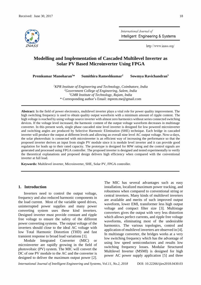
The block diagram for the proposed work is
shown in Fig. 1. Cascaded H-bridge multilevel
inverter consists of four full bridge inverters, four
transformers connected in series on the secondary
side of the transformer. Each bridge can create three
different voltage levels in AC output voltage
waveform and the system allowing an overall nine
level AC output voltage.
FPGA controller is used to generate gate pulses
and desired switching angle is decided by employing
SHE technique. The power circuit consists of four H-
bridges and transformers and it derives the input from
24 cell solar PV module through the DC-DC
converter [14, 15] for maintaining the constant input
voltage to the inverter power circuit. The function of
opto coupler is to isolate the control circuit from the
Figure.1 Block diagram of FPGA based 9-level cascaded
multilevel inverter
Received: June 30, 2017 20
International Journal of Intelligent Engineering and Systems, Vol.11, No.2, 2018 DOI: 10.22266/ijies2018.0430.03
power circuit. It is essential to provide isolation
circuit between power circuit and control circuit or
else the high power components may damage the low
power PWM circuit components. MOSFET drive
circuit is designed to connect the gate directly to a
voltage bus with no intervening resistance other than
the impedance of the drive circuit switch. Gate driver
acts as a high-power buffer stage between the PWM
output of the control device and gates of the primary
power switching MOSFETs.
2.1 Power system harmonics
The output current waveforms are distorted from
sine wave at fundamental frequency since the
nonlinear loads are represented as current sources.
Those loads will draw non-sinusoidal currents from
the given power source. Depends on the equipment
design, the AC line current is of square wave or a
stepped wave. The analysis can be done on the square
wave or stepped wave into its equivalent sinusoidal
waves of higher frequencies. Then there is a
harmonic voltage drop on the power source due to
this harmonic currents. This results voltage distortion
in power source and the harmonic currents will flows
through components and loads.
Harmonic distortion on the waveform is nothing
but electrical noise. It will superposition on the
signals, which are of multiples of fundamental
frequency. Multiplying of power electronic systems
results in high harmonic distortion. This results in
reduction of power quality and power systems
stability. Harmonic problems include variety of
electrical disturbances, which may originate in many
ways and have different effects on various sensitive
loads. Low variations in power source is not noticed
in the operation of conventional equipment. As a
result, increasing numbers of industrial and
commercial facilities are trying to protect by
investing in sophisticated and safe equipment to
improve power quality. Moreover, the production of
nonlinear loads with large power has increased the
noise level in voltage and current waveforms, forcing
to improve the compensation characteristics required
to satisfy additional rigid harmonics standard.
The most commonly used harmonic index is
represented in Eq. (1) and (2).
𝑇𝐻𝐷𝑣 =√∑ 𝑉ℎ=2∝
ℎ=2
𝑉1 (1)
𝑇𝐻𝐷𝑖 =√∑ 𝑉ℎ=2∝
ℎ=2
𝐼1 (2)
Table 1. IEEE standard for voltage harmonics - (IEEE
519 – voltage distortion limits)
Bus voltage Individual Vh (%) THDv (%)
V < 69 kV 3.0 5.5
69 kV-161 kV 1.5 2.5
V=161 kV 1 1.5
Table 2. IEEE standard for current harmonics - general
distribution systems (120V – 69 kV)
ISC /
IL
H<
11
H=
11-17
H=
17-23
H=
23-35
H=
35
THDi
(%)
<20 4 2 1.5 0.6 0.3 5.5
20-50 7.0 3.5 2.5 1.0 0.5 8
50-
100 10 4.5 4.0 1.5 0.7 12
100-
1000 12 5.5 5.0 2.0 1.0 15
>1000 15 7.0 6.0 2.5 1.4 20
The harmonic index is used to measure the
deviation of a periodic harmonics from pure sine
wave. For pure sine wave at fundamental frequency,
the THD is almost zero. Similarly, the measures of
individual harmonic distortion for voltage and
current at ‘h’ order are defined as Vh/V1 and Ih/I1
respectively.
Harmonic standards such as IEEE 519-1992 and
IEC 1003-3-2 are tabulated in Table 1-2 emphasize
placement of limits on harmonic currents produced
by the loads for customers and harmonic voltage
distortion for the electric utilities. Electrical system
has impedance that varies with frequency and a
frequency with high system impedance is called
resonant frequency. When a VFD or other non-linear
device injects a harmonic current at the resonant
frequency, the system becomes unstable. Ohms law
holds for system resonances. When both current and
impedance are high at the same time, voltage goes
exceptionally high and causes excessive heating or
immediate dielectric failures in capacitors,
transformers or other installed devices.
2.2 Multilevel inverter topology
Multilevel inverters replace the traditional multi-
pulse converters with/without the need for
transformers. The three multilevel inverter topology
[16] may be used in reactive power compensation
without voltage imbalance problem. Cascaded
multilevel inverter with separate DC source will
introduce short circuiting when the back-back
inverters are not turned on synchronously.
So, to overcome the short circuiting problem,
Received: June 30, 2017 21
International Journal of Intelligent Engineering and Systems, Vol.11, No.2, 2018 DOI: 10.22266/ijies2018.0430.03
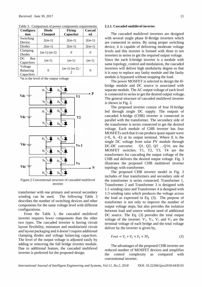
Table 3. Comparison of power components requirements
Configura
tion
Diode
Clamped
Flying
Capacitor
Cascad
ed
Switching
Device 2(m-1) 2(m-1) 2(m-1)
Diodes 2(m-1) 2(m-1) 2(m-1)
Clamping
Diodes (m-1) (m-2) 0 0
DC Bus
Capacitors (m-1) (m-1) (m-1)
Voltage
Balancing
Capacitors
0 (m-1) (m-2) /
2 0
*m is the level of the output voltage
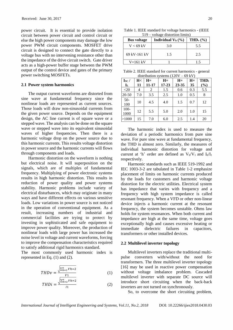
Figure.2 Conventional structure of cascaded multilevel
inverter
transformer with one primary and several secondary
winding can be used. The following Table 3
describes the number of switching devices and other
components for the same voltage level with different
configurations.
From the Table 3, the cascaded multilevel
inverter requires fewer components than the other
two types. The cascaded inverter is having circuit
layout flexibility, miniature and modularized circuit
and layout packaging and it doesn’t require additional
clamping diodes and voltage balancing capacitors.
The level of the output voltage is adjusted easily by
adding or removing the full bridge inverter module.
Due to additional feature, the cascaded multilevel
inverter is preferred for the proposed design.
2.2.1. Cascaded multilevel inverter
The cascaded multilevel inverters are designed
with several single phase H-Bridge inverters which
are connected in series. By using proper switching
device, it is capable of delivering moderate voltage
levels and this inverter is formed with three to ten
inverters in series to get the required output voltage.
Since the each h-bridge inverter is a module with
same topology, control and modulation, the cascaded
inverters will deliver high modularity degree so that
it is easy to replace any faulty module and the faulty
module is bypassed without stopping the load.
The power MOSFET is selected to design the H-
bridge module and DC source is associated with
separate module. The AC output voltage of each level
is connected in series to get the desired output voltage.
The general structure of cascaded multilevel inverter
is shown in Fig. 2.
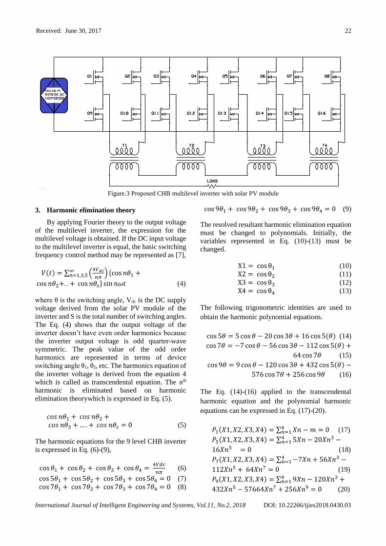
The proposed inverter consist of four H-bridge
fed through single DC supply. The outputs of
cascaded h-bridge (CHB) inverter is connected in
parallel with the transformer. The secondary side of
the transformer is series connected to get the desired
voltage. Each module of CHB inverter has four
MOSFETs such that it can produce quasi square wave
(+E, 0, -E) at its output terminal. Where E is the
single DC voltage from solar PV module through
DC-DC converter. Q1, Q2, Q3 …Q16, are the
MOSFET switches. T1, T2, T3, T4 are the
transformers for cascading the output voltage of the
CHB and delivers the desired output voltage. Fig. 3
illustrates the proposed CHB multilevel inverter
topology with transformer.
The proposed CHB inverter model in Fig. 3
includes of four transformers and secondary side of
the transformer is series connected. Transformer 1,
Transformer 2 and Transformer 3 is designed with
1:1 winding ratio and Transformer 4 is designed with
1:3 winding ratio which produces the voltage across
the load as expressed in Eq. (3). The purpose of
transformer is not only to improve the number of
output voltage steps, but also provides the isolation
between load and source without need of additional
DC source. The Eq. (3) provides the total output
voltage of the inverter. V1, V2, V3 and V4 are the
terminal voltage of each bridge and the total voltage
deliver by the inverter is given by,
𝑉𝑜𝑢𝑡 = 𝑉1 + 𝑉2 + 𝑉3 + 3𝑉4 (3)
The advantages of the proposed CHB inverter are
reduced number of MOSFET devices and simplifies
the control complexity as compared with
conventional inverter.
Received: June 30, 2017 22
International Journal of Intelligent Engineering and Systems, Vol.11, No.2, 2018 DOI: 10.22266/ijies2018.0430.03
Figure.3 Proposed CHB multilevel inverter with solar PV module
3. Harmonic elimination theory
By applying Fourier theory to the output voltage
of the multilevel inverter, the expression for the
multilevel voltage is obtained. If the DC input voltage
to the multilevel inverter is equal, the basic switching
frequency control method may be represented as [7],
𝑉(𝑡) = ∑ (4𝑉𝑑𝑐
𝑛𝜋) {cos 𝑛𝜃1 +∞
𝑛=1,3,5
cos 𝑛𝜃2+. . + cos 𝑛𝜃𝑠} sin 𝑛𝜔𝑡 (4)
where θ is the switching angle, Vdc is the DC supply
voltage derived from the solar PV module of the
inverter and S is the total number of switching angles.
The Eq. (4) shows that the output voltage of the
inverter doesn’t have even order harmonics because
the inverter output voltage is odd quarter-wave
symmetric. The peak value of the odd order
harmonics are represented in terms of device
switching angle θ1, θ2, etc. The harmonics equation of
the inverter voltage is derived from the equation 4
which is called as transcendental equation. The nth
harmonic is eliminated based on harmonic
elimination theorywhich is expressed in Eq. (5).
𝑐𝑜𝑠 𝑛𝜃1 + 𝑐𝑜𝑠 𝑛𝜃2 + 𝑐𝑜𝑠 𝑛𝜃3 + … . + 𝑐𝑜𝑠 𝑛𝜃𝑠 = 0 (5)
The harmonic equations for the 9 level CHB inverter
is expressed in Eq. (6)-(9),
cos 𝜃1 + cos 𝜃2 + cos 𝜃3 + cos 𝜃4 = 4𝑉𝑑𝑐
𝑛𝜋 (6)
cos 5𝜃1 + cos 5𝜃2 + cos 5𝜃3 + cos 5𝜃4 = 0 (7)
cos 7𝜃1 + cos 7𝜃2 + cos 7𝜃3 + cos 7𝜃4 = 0 (8)
cos 9𝜃1 + cos 9𝜃2 + cos 9𝜃3 + cos 9𝜃4 = 0 (9)
The resolved resultant harmonic elimination equation
must be changed to polynomials. Initially, the
variables represented in Eq. (10)-(13) must be
changed.
X1 = cos θ1 (10)
X2 = cos θ2 (11)
X3 = cos θ3 (12)
X4 = cos θ4 (13)
The following trigonometric identities are used to
obtain the harmonic polynomial equations.
cos 5𝜃 = 5 cos 𝜃 − 20 cos 3𝜃 + 16 cos 5(𝜃) (14)
cos 7𝜃 = −7 cos 𝜃 − 56 cos 3𝜃 − 112 cos 5(𝜃) +
64 cos 7𝜃 (15)
cos 9𝜃 = 9 cos 𝜃 − 120 cos 3𝜃 + 432 cos 5(𝜃) −
576 cos 7𝜃 + 256 cos 9𝜃 (16)
The Eq. (14)-(16) applied to the transcendental
harmonic equation and the polynomial harmonic
equations can be expressed in Eq. (17)-(20).
𝑃1(𝑋1, 𝑋2, 𝑋3, 𝑋4) = ∑ 𝑋𝑛 − 𝑚 = 04𝑛=1 (17)
𝑃5(𝑋1, 𝑋2, 𝑋3, 𝑋4) = ∑ 5𝑋𝑛 − 20𝑋𝑛3 −4𝑛=1
16𝑋𝑛5 = 0 (18)
𝑃7(𝑋1, 𝑋2, 𝑋3, 𝑋4) = ∑ −7𝑋𝑛 + 56𝑋𝑛3 −4𝑛=1
112𝑋𝑛5 + 64𝑋𝑛7 = 0 (19)
𝑃9(𝑋1, 𝑋2, 𝑋3, 𝑋4) = ∑ 9𝑋𝑛 − 120𝑋𝑛3 +4𝑛=1
432𝑋𝑛5 − 57664𝑋𝑛7 + 256𝑋𝑛9 = 0 (20)
Received: June 30, 2017 23
International Journal of Intelligent Engineering and Systems, Vol.11, No.2, 2018 DOI: 10.22266/ijies2018.0430.03
From the above equations, the total harmonic
distortion for the inverter output voltage is given in
Eq. (21),
%𝑇𝐻𝐷 = √𝑉𝑎𝑐
2− 𝑉𝑎𝑐12
𝑉𝑎𝑐12 (21)
where Vac is rms value of the output voltage and Vac1
is rms value of the fundamental voltage.
3.1 Switching angle analysis
The property of the inverter output voltage
waveform id determined by the modulation technique
on the proposed converter. The SHE technique is
used to get the 9-level of output voltage. So that the
switching angle is selected carefully to
avoid/eliminate the odd order harmonics. The SHE
technique not only produce the desired switching
angle to get output voltage and also minimizes the
total harmonic distortion [8]. It also reduces the
amount electromagnetic interference and loss due to
higher frequency switching.
For the given a desired reference voltage V from
equation 4, it is necessary to find the switching angles,
θ1, θ2, θ3,… θs, such a way that, the THD of the output
voltage will be minimize. From equation 4, the
Fourier coefficients magnitude with respect to the
reference voltage when normalized is expressed in Eq.
(22).
𝑉 = (4𝑉𝑑𝑐
𝜋) {cos 𝜃1 + cos 𝜃2 +
cos 𝜃3 + … . + cos 𝑛𝜃𝑠} (22)
The fundamental component amplitude is controlled
by the modulation index (M) and is represented in Eq.
(23),
𝑀 =𝑉
𝑉𝑑𝑐 (23)
where V is the peak value of the output voltage of the
inverter.
The Degree of Freedom (DoF) for the CHB
inverter which employs SHE technique is S; one of
the DoF is selected to find the value of the output
voltage presented in Eq. (24) and the remaining DoF
is to eliminate harmonic component. By employing
SHE, higher order odd harmonic (S-1) will be
eliminated.
cos 𝜃1 + cos 𝜃2+ . . + cos 𝑛𝜃16 =𝑀𝜋
4 (24)
The non-linear transcendental equation which is
given in Eq. (4) is solved to determine the
approximate value of the switching angle and it must
capable to eliminate the harmonics at selected
modulation index. It is not possible to find the very
accurate solution, because of the non-linearity of the
harmonic equation using ordinary mathematical
methods. By considering the various factor, Half
Equal Phase method is used to produce the switching
angles in a best way and it will give the better output
waveform, which is in the area between 0 to π/2. The
switching angle is given by the Eq. (25),
𝜃𝑖 = 𝑖 90𝑜
𝑚+1
2
= 𝑖 180𝑜
𝑚+1 (25)
where, i = 1,2, ……. 𝑚+1
2 and m is the level of the
inverter output voltage. The Eq. (25) is adjusted to
extend the switching angle between 0 to 2π. So that,
the possible switching angle combinations may also
be obtained.
4. Results and discussion
4.1 Simulation of proposed inverter
The validation of single phase 9-level cascaded
H-bridge microinverter has been done with the help
of Matlab/Simulink dynamic simulation software is
shown in Fig. 4. The switching angle for the gate
signals are achieved by SHE technique which
controls sixteen MOSFET switches to get the
required output voltage. The gate signal produced by
SHE technique is shown in Fig. 5.
In any of the 4 H-bridge module, triggering of
MOSFET on the same leg should be avoided to avoid
short-circuiting the DC voltage which is derived from
24 cell solar PV module. The load output voltage and
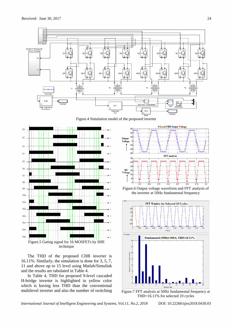
FFT analysis for the proposed inverter is shown
in Fig. 6 at fundamental frequency of about 50 Hz.
The FFT analysis for the selected 10 cycles is
shown in Fig. 7, it can be seen that, there is
remarkable change in THD from conventional
cascaded H-bridge inverter to the proposed inverter
as 28.5% to 16.11%, because of new inverter
topology and switching angle control. The low
switching frequency is required for high power
application but the proposed inverter is used as
microinverter which is designed for less power rating
(<100W). So, the CHB inverter requires high
switching frequency which will high power quality
and high range of bandwidth.
Received: June 30, 2017 24
International Journal of Intelligent Engineering and Systems, Vol.11, No.2, 2018 DOI: 10.22266/ijies2018.0430.03
Figure.4 Simulation model of the proposed inverter
Figure.5 Gating signal for 16 MOSFETs by SHE
technique
The THD of the proposed CHB inverter is
16.11%. Similarly, the simulation is done for 3, 5, 7,
11 and above up to 15 level using Matlab/Simulink
and the results are tabulated in Table 4.
In Table 4, THD for proposed 9-level cascaded
H-bridge inverter is highlighted in yellow color
which is having less THD than the conventional
multilevel inverter and also the number of switching
Figure.6 Output voltage waveform and FFT analysis of
the inverter at 50Hz fundamental frequency
Figure.7 FFT analysis at 50Hz fundamental frequency at
THD=16.11% for selected 10 cycles
Received: June 30, 2017 25
International Journal of Intelligent Engineering and Systems, Vol.11, No.2, 2018 DOI: 10.22266/ijies2018.0430.03
Table 4. %THD on different levels of the output voltage
@14.4V constant input
S.No.
Number
of
Output
Voltage
Levels
%THD at Fundamental
Frequency of
50 Hz
Conventional
CHB
Multilevel
Inverter
Proposed
CHB
Multilevel
Inverter
1 3 37.70 29.45
2 5 28.83 21.79
3 7 28.83 19.24
4 9 27.41 16.11
5 11 17.48 11.36
6 13 15.78 9.65
7 15 10.74 8.71
devices are reduce. So that, the switching loss and
conduction loss is reduced than the conventional and
offers good performance. The higher output voltage
level is having less THD than the conventional but it
requires more switching devices which increases the
complexity and also the overall loss is proportionally
increased.
4.2 Hardware implementation of CHB 9-level
inverter
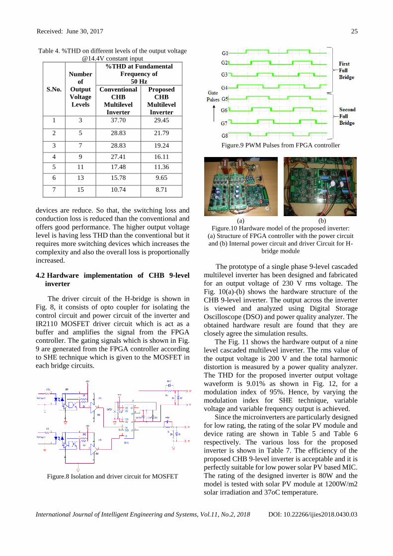
The driver circuit of the H-bridge is shown in
Fig. 8, it consists of opto coupler for isolating the
control circuit and power circuit of the inverter and
IR2110 MOSFET driver circuit which is act as a
buffer and amplifies the signal from the FPGA
controller. The gating signals which is shown in Fig.
9 are generated from the FPGA controller according
to SHE technique which is given to the MOSFET in
each bridge circuits.
Figure.8 Isolation and driver circuit for MOSFET
Figure.9 PWM Pulses from FPGA controller
(a) (b)
Figure.10 Hardware model of the proposed inverter:
(a) Structure of FPGA controller with the power circuit
and (b) Internal power circuit and driver Circuit for H-
bridge module
The prototype of a single phase 9-level cascaded
multilevel inverter has been designed and fabricated
for an output voltage of 230 V rms voltage. The
Fig. 10(a)-(b) shows the hardware structure of the
CHB 9-level inverter. The output across the inverter
is viewed and analyzed using Digital Storage
Oscilloscope (DSO) and power quality analyzer. The
obtained hardware result are found that they are
closely agree the simulation results.
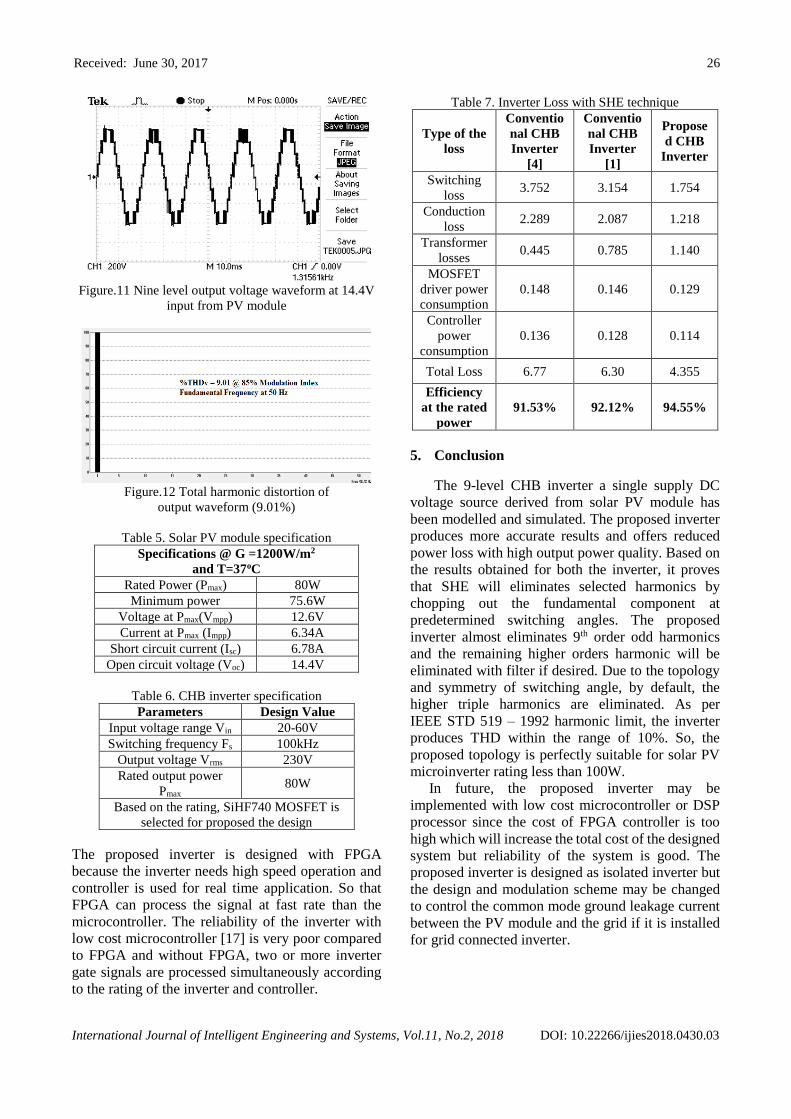
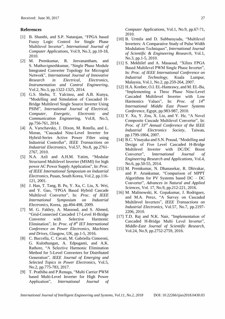
The Fig. 11 shows the hardware output of a nine
level cascaded multilevel inverter. The rms value of
the output voltage is 200 V and the total harmonic
distortion is measured by a power quality analyzer.
The THD for the proposed inverter output voltage
waveform is 9.01% as shown in Fig. 12, for a
modulation index of 95%. Hence, by varying the
modulation index for SHE technique, variable
voltage and variable frequency output is achieved.
Since the microinverters are particularly designed
for low rating, the rating of the solar PV module and
device rating are shown in Table 5 and Table 6
respectively. The various loss for the proposed
inverter is shown in Table 7. The efficiency of the
proposed CHB 9-level inverter is acceptable and it is
perfectly suitable for low power solar PV based MIC.
The rating of the designed inverter is 80W and the
model is tested with solar PV module at 1200W/m2
solar irradiation and 37oC temperature.
Received: June 30, 2017 26
International Journal of Intelligent Engineering and Systems, Vol.11, No.2, 2018 DOI: 10.22266/ijies2018.0430.03
Figure.11 Nine level output voltage waveform at 14.4V
input from PV module
Figure.12 Total harmonic distortion of
output waveform (9.01%)
Table 5. Solar PV module specification
Specifications @ G =1200W/m2
and T=37oC
Rated Power (Pmax) 80W
Minimum power 75.6W
Voltage at Pmax(Vmpp) 12.6V
Current at Pmax (Impp) 6.34A
Short circuit current (Isc) 6.78A
Open circuit voltage (Voc) 14.4V
Table 6. CHB inverter specification
Parameters Design Value
Input voltage range Vin 20-60V
Switching frequency Fs 100kHz
Output voltage Vrms 230V
Rated output power
Pmax 80W
Based on the rating, SiHF740 MOSFET is
selected for proposed the design
The proposed inverter is designed with FPGA
because the inverter needs high speed operation and
controller is used for real time application. So that
FPGA can process the signal at fast rate than the
microcontroller. The reliability of the inverter with
low cost microcontroller [17] is very poor compared
to FPGA and without FPGA, two or more inverter
gate signals are processed simultaneously according
to the rating of the inverter and controller.
Table 7. Inverter Loss with SHE technique
Type of the
loss
Conventio
nal CHB
Inverter
[4]
Conventio
nal CHB
Inverter
[1]
Propose
d CHB
Inverter
Switching
loss 3.752 3.154 1.754
Conduction
loss 2.289 2.087 1.218
Transformer
losses 0.445 0.785 1.140
MOSFET
driver power
consumption
0.148 0.146 0.129
Controller
power
consumption
0.136 0.128 0.114
Total Loss 6.77 6.30 4.355
Efficiency
at the rated
power
91.53% 92.12% 94.55%
5. Conclusion
The 9-level CHB inverter a single supply DC
voltage source derived from solar PV module has
been modelled and simulated. The proposed inverter
produces more accurate results and offers reduced
power loss with high output power quality. Based on
the results obtained for both the inverter, it proves
that SHE will eliminates selected harmonics by
chopping out the fundamental component at
predetermined switching angles. The proposed
inverter almost eliminates 9th order odd harmonics
and the remaining higher orders harmonic will be
eliminated with filter if desired. Due to the topology
and symmetry of switching angle, by default, the
higher triple harmonics are eliminated. As per
IEEE STD 519 – 1992 harmonic limit, the inverter
produces THD within the range of 10%. So, the
proposed topology is perfectly suitable for solar PV
microinverter rating less than 100W.
In future, the proposed inverter may be
implemented with low cost microcontroller or DSP
processor since the cost of FPGA controller is too
high which will increase the total cost of the designed
system but reliability of the system is good. The
proposed inverter is designed as isolated inverter but
the design and modulation scheme may be changed
to control the common mode ground leakage current
between the PV module and the grid if it is installed
for grid connected inverter.
Received: June 30, 2017 27
International Journal of Intelligent Engineering and Systems, Vol.11, No.2, 2018 DOI: 10.22266/ijies2018.0430.03
References
[1] B. Shanthi, and S.P. Natarajan, “FPGA based
Fuzzy Logic Control for Single Phase
Multilevel Inverter”, International Journal of
Computer Applications, Vol.9, No.3, pp.10-18,
2010.
[2] M. Premkumar, R. Jeevanantham, and
S. Muthuvigneshkumar, “Single Phase Module
Integrated Converter Topology for Microgrid
Network”, International Journal of Innovative
Research in Electrical, Electronics,
Instrumentation and Control Engineering,
Vol.2, No.3, pp.1322-1325, 2014.
[3] G.S. Shehu, T. Yalcinoz, and A.B. Kunya,
“Modelling and Simulation of Cascaded H-
Bridge Multilevel Single Source Inverter Using
PSIM”, International Journal of Electrical,
Computer, Energetic, Electronic and
Communication Engineering, Vol.8, No.5,
pp.756-761, 2014.
[4] A. Varschavsky, J. Dixon, M. Rotella, and L.
Moran, “Cascaded Nine-Level Inverter for
Hybrid-Series Active Power Filter using
Industrial Controller”, IEEE Transactions on
Industrial Electronics, Vol.57, No.8, pp.2761-
2767, 2010.
[5] N.A. Azli and A.H.M. Yatim, “Modular
Structured Multilevel Inverter (MSMI) for high
power AC Power Supply Application”, In: Proc.
of IEEE International Symposium on Industrial
Electronics, Pusan, South Korea, Vol.2, pp.116-
121, 2001.
[6] J. Han, T. Tang, B. Pu, Y. Xu, C. Liu, X. Wei,
and Y. Gao, “FPGA Based Hybrid Cascade
Multilevel Converter”, In: Proc. of IEEE
International Symposium on Industrial
Electronics, Korea, pp.494-498, 2009.
[7] M. G. Fakhry, A. Massoud, and S. Ahmed,
“Grid-Connected Cascaded 17-Level H-Bridge
Converter with Selective Harmonic
Elimination”, In: Proc. of 8th IET International
Conference on Power Electronics, Machines
and Drives, Glasgow, UK, pp.1-5, 2016.
[8] C. Buccella, C. Cecati, M. Gabriella Cimoroni,
G. Kulothungan, A. Edpuganti, and A.K.
Rathore, “A Selective Harmonic Elimination
Method for 5-Level Converters for Distributed
Generation”, IEEE Journal of Emerging and
Selected Topics in Power Electronics, Vol.5,
No.2, pp.775-783, 2017.
[9] T. Prathiba and P.Renuga, “Multi Carrier PWM
based Multi-Level Inverter for High Power
Application”, International Journal of
Computer Applications, Vol.1, No.9, pp.67-71,
2010.
[10] B. Urmila and D. Subbarayudu, “Multilevel
Inverters: A Comparative Study of Pulse Width
Modulation Techniques”, International Journal
of Scientific & Engineering Research, Vol.1,
No.3, pp.1-5, 2010.
[11] S. Mekhilef and A. Masaoud, “Xilinx FPGA
Based Multilevel PWM Single Phase Inverter”,
In: Proc. of IEEE International Conference on
Industrial Technology, Kuala Lumpur,
Malaysia, Vol.1, No.2, pp.259-264, 2007.
[12] H.A. Konber, O.I. EL-Hamrawy, and M. EL-Ba,
“Implementing a Three Phase Nine-Level
Cascaded Multilevel Inverter with Low
Harmonics Values”, In: Proc. of 14th
International Middle East Power Systems
Conference, Egypt, pp.983-987, 2010.
[13] Y. Xu, Y. Zou, X. Liu, and Y. He, “A Novel
Composite Cascade Multilevel Converter”, In:
Proc. of 33rd Annual Conference of the IEEE
Industrial Electronics Society, Taiwan,
pp.1799-1804, 2007.
[14] B.C. Vinayaka and S.N. Prasad, “Modelling and
Design of Five Level Cascaded H-Bridge
Multilevel Inverter with DC/DC Boost
Converter”, International Journal of
Engineering Research and Applications, Vol.4,
No.6, pp.50-55, 2014.
[15] M. Premkumar, N. Dhanasekar, R. Dhivakar,
and P. Arunkumar, “Comparison of MPPT
Algorithms for PV Systems based DC – DC
Converter”, Advances in Natural and Applied
Sciences, Vol. 17, No.9, pp.212-221, 2016.
[16] M. Malinowski, K. Gopakumar, J. Rodriguez,
and M.A. Perez, “A Survey on Cascaded
Multilevel Inverters”, IEEE Transactions on
Industrial Electronics, Vol.57, No.7, pp.2197-
2206, 2010.
[17] T.D. Raj and N.K. Nair, “Implementation of
Cascaded H-Bridge Multi Level Inverter”,
Middle-East Journal of Scientific Research,
Vol.24, No.9, pp.2752-2759, 2016.


