Embed Size (px)
Citation preview

1
ABSTRACT
The project we have undertaken is “Design and Simulation of Five Level Cascaded
Inverter Using Multilevel Sinusoidal PWM Strategies”. Five Level Cascaded Inverter
as compared to single level inverter have advantages like minimum harmonic
distortion reduced EMI/RFI generation and can operate on several voltage levels.
The Multi-level inverter is to synthesize a near sinusoidal voltage from several levels
of dc voltages. As number of levels increases, the synthesized output waveform has
more steps, which provides a staircase wave that approaches a desired waveform.
Also, as steps are added to waveform, the harmonic distortion of the output wave
decreases, approaching zero as the number of voltage levels increases. Three phases
two level inverter is one of the popular multi-level inverter, designed using
Bidirectional chopper cells.
Multi-level inverter is being utilized for multipurpose applications such as active
power filters, static VAR compensator and machine drives for sinusoidal and
trapezoidal current applications. The active power filters are modelled with the
inverters and suitable switching control strategies (PWM technique) to carry out
harmonic elimination.

2
CHAPTER 1
INTRODUCTION
1.1 INTRODUCTION
Conventionally, there are two ways in which electrical power is transmitted.
Direct current (DC) comes from a source of constant voltage and is suited to short-
range or device level transmission. Alternating current (AC) power consists of a
sinusoidal voltage source in which a continuously changing voltage (and current) can
be used to employ magnetic components. Long distance electrical transmission favors
AC power, since the voltage can be boosted easily with the use of transformers. By
boosting the voltage, less current is needed to deliver a given amount of power to a
load, reducing the resistive loss through conductors.
The adoption of AC power has created a trend where most devices adapt AC power
from an outlet into DC power for use by the device. However, AC power is not
always available and the need for mobility and simplicity has given batteries an
advantage in portable power. Thus, for portable AC power, inverters are needed.
Inverters take a DC voltage from a battery or a solar panel as input, and convert it into
an AC voltage output.
There are three types of DC/AC inverters available on the market, which are classified
by their output type: square wave, modified-sine wave and pure sine wave. Off-the-
shelf inverters are generally either square wave or modified-sine wave. These types of
inverters are less expensive to make and the output, though delivering the same
average voltage to a load, is not appropriate to delicate electronic devices which rely
on precise timing. Pure sine wave inverters offer more accuracy and less unused
harmonic energy delivered to a load, but they are more complex in design and more
expensive. Pure sine wave inverters will power devices with more accuracy, less
power loss, and less heat generation.
Pure sine wave inversion is accomplished by taking a DC voltage source and
switching it across a load using an H-bridge. If this voltage needs to be boosted from
the DC source, it can be accomplished either before the AC stage by using a DC-DC

3
boost converter, or after the AC stage by using a boost transformer. The inverted
signal itself is composed of a pulse-width-modulated (PWM) signal which encodes a
sine wave. The duty cycle of the output is changed such that the power transmitted is
exactly that of a sine-wave. This output can be used as-is or, alternatively, can be
filtered easily into a pure sine wave. This report documents the design of a true sine
wave inverter, focusing on the inversion of a DC high-voltage source. It therefore
assumes the creation of a DC-DC boost phase.
1.2 FIVE LEVEL CASCADED INVERTER
Multilevel inverter is a power electronic system that synthesizes a desired voltage
from several levels of direct current voltage as inputs. The advantages of using
multilevel topology include reduction of power ratings of power devices and lower
cost. There are three topologies - diode clamped inverter, flying capacitor inverter and
cascaded inverter.

4
CHAPTER 2
LITRETURE SURVEY
2.1 INTRODUCTION
Electrical power transmission is classified into two methods: alternating current
and direct current. Alternating current can be found in AC motor drives and long
distance power transmission. The cyclic nature of alternating current enables the use
of transformers, which use magnetic principles to alter voltage levels. By stepping up
an AC voltage, a large amount of power can be transferred over a long distance with
less energy lost in heating up a conductor due to a lower current requirement, since
P=I2R. As such, AC power is more conventional than high voltage DC systems due to
the ease of stepping up voltage for transmission and stepping voltage down to
household outlet levels.
DC voltage also has a place in powering devices. Wherever there is a changing
electrical current, a changing magnetic field accompanies it. In a device-level
electrical circuit, the magnetic variations introduced by AC current manifest
themselves as electrical noise. The effects of this can range from audible line hum in
an audio system to inaccurate measurements in an electronic instrument. Thus, it is
commonplace for a device such as an MP3 player to employ DC voltages that have
been rectified and filtered from an AC wall outlet. An MP3 player also proves one
other benefit of DC power transmission.
It can be done with a compact form factor. Without a need for transformers or
switching circuitry, battery-powered MP3 players, or any other portable device, can
be made small enough to fit into a pocket.
However, there may come a time when household AC power is cut off due to a power
outage. The multitude of devices that are designed around AC/DC power conversion
(computers, for example) would then no longer be able to operate. One solution to this
problem is an auxiliary AC power generator, like those powered by gasoline engines,
or DC/AC power inverters which use energy stored in batteries (a DC source) and
5
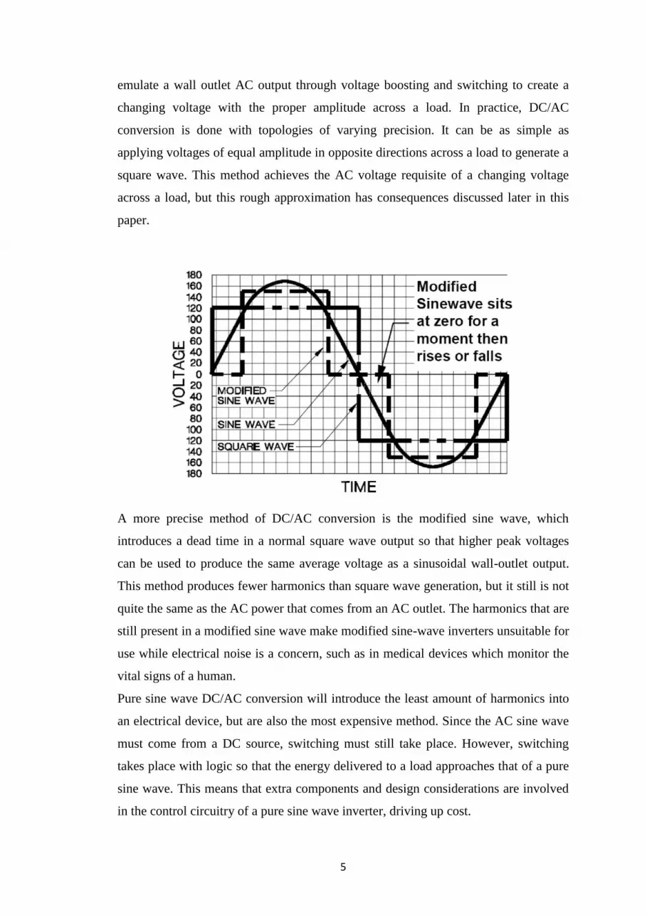
emulate a wall outlet AC output through voltage boosting and switching to create a
changing voltage with the proper amplitude across a load. In practice, DC/AC
conversion is done with topologies of varying precision. It can be as simple as
applying voltages of equal amplitude in opposite directions across a load to generate a
square wave. This method achieves the AC voltage requisite of a changing voltage
across a load, but this rough approximation has consequences discussed later in this
paper.
A more precise method of DC/AC conversion is the modified sine wave, which
introduces a dead time in a normal square wave output so that higher peak voltages
can be used to produce the same average voltage as a sinusoidal wall-outlet output.
This method produces fewer harmonics than square wave generation, but it still is not
quite the same as the AC power that comes from an AC outlet. The harmonics that are
still present in a modified sine wave make modified sine-wave inverters unsuitable for
use while electrical noise is a concern, such as in medical devices which monitor the
vital signs of a human.
Pure sine wave DC/AC conversion will introduce the least amount of harmonics into
an electrical device, but are also the most expensive method. Since the AC sine wave
must come from a DC source, switching must still take place. However, switching
takes place with logic so that the energy delivered to a load approaches that of a pure
sine wave. This means that extra components and design considerations are involved
in the control circuitry of a pure sine wave inverter, driving up cost.

6
2.2 PROBLEM STATEMENT
In developing countries, healthcare is often of limited access to the local inhabitants.
The government is often unable, or unwilling, to direct its attention to the issue of
public healthcare because the country is not yet economically or technologically
mature enough to support a quality healthcare system. The lack of money available
for building a reliable electrical infrastructure stunts the growth of electronics use,
which includes the employment of instruments used in modern healthcare. In African
villages, villagers may install a solar panel on their homes for the sole reason of
charging a cell phone because there are no centralized production facilities or
transmission lines for electrical energy.
The lack of reliable power severely limits the quality of healthcare available in
developing countries. While it is true that these countries receive donations of medical
instruments, the means to operate them reliably often does not exist. An ongoing issue
with poorly developed electrical grids is that the production of electricity is not
enough to meet demand. Brown-outs are commonplace, and the transients that result
damage the donated equipment used in medical procedures. Imagine, during an
operation, that a patient’s heart stopped and no defibrillator was available because the
grid suffered a brownout. Sadly, this is an all-too-common occurrence in much of the
underdeveloped world.
2.3 OBJECTIVE AND SCOPE
Due to these problems, there is a market for uninterruptible power supplies which can
provide a temporary remedy to the lack of electrical infrastructure in developing
countries. Enter Waste to Watts, a company devoted to the recycling of electronic
waste into useful products in developing countries. Their proposed flagship product,
the ENZI interface, is a multipurpose power conditioner that will be compatible with
grid power, battery, and solar power inputs to provide uninterrupted power. The
mandatory characteristics of the ENZI interface are that it will be affordable have
high manufacturability, make use of waste electronic components local to the places
they will be used, be capable of reliably powering medical equipment, and tolerate a
wide range of power sources.

7
2.4 RESEARCH
2.4.1 SOURCES OF INFORMATION
In the recent past, the multilevel inverters have drawn tremendous attention in the
field of high voltage and high power applications. In the researches on multilevel
inverters, determination of their respective control strategies is the emerging topic
which has been discussed in the previous chapter. One of the most important
problems in controlling a multilevel voltage source inverter is to obtain a variable
amplitude and frequency sinusoidal output by employing simple control techniques.
Indeed, in voltage source inverters, non-fundamental current harmonics cause power
losses, electromagnetic interference and pulsating torques in AC motor drives.
Harmonic reduction can then be strictly related to the performance of an inverter with
any switching strategy. In multilevel voltage source inverters, various Pulse Width
Modulation control schemes have been developed and the same were analyzed in the
previous chapter with respect to reduction in power quality issues as discussed by
Corzine et al (2003).
Multilevel inverter can increase the power by (m-1) times than that of two level
inverter through the series and parallel connection of power semiconductor switches.
Comparing this with two level inverter systems delivering same power, multilevel
inverter has the advantages that the lower harmonic components on the output
voltages can be eliminated and EMI problem could be decreased. Due to these merits,
many studies on multilevel inverters have been performed at simulations and very few
with the hardware implementations.
2.4.2 REQUIRED INPUT DATA
Design of multilevel inverter is made based on the following data:
1. Number of semiconductor devices used per phase leg.
2. Number of DC bus capacitors used.
3. Number of balancing capacitors used per phase leg.
4. Amplitude of fundamental and dominant harmonic components.
5. Total Harmonic Distortion of output voltage.
6. Control complexity based on voltage unbalances and power switches.

8
With the available facts, evidently we can conclude that cascaded multilevel inverter
is more efficient than other topologies of multilevel inverter.
Table 2.1 Comparison of different multilevel inverter topologies
S.No. Topology Diode
Clamped
Flying
Capacitor Cascaded
1 Power semiconductor
switches
2(m-1) 2(m-1) 2(m-1)
2 Clamping diodes per
phase
(m-1)(m-2) 0 0
3 DC bus capacitors (m-1) (m-1) (m-1)/2
4 Balancing capacitors per
phase
0 (m-1)(m-2)/2 0
5 Voltage unbalancing Average High very small
6 Applications Motor drive
system,
STATCOM
Motor drive
system,
STATCOM
Motor drive
system, PV,
fuel cells,
battery system
2.4.3 DESIGN APPROACHES
To solve this problem, two or more power switches can be connected in series in
order to provide the desired voltage rating. However, the characteristics of devices of
the same type are not identical. For the same OFF state current, their OFF state
voltages differ. Even during the turn OFF of the switches the variations in stored
charges cause difference in the reverse voltage sharing. The switch with the least
recovered charge faces the highest transient voltage. For higher current handling, the
switches are connected in parallel, however because of uneven switch characteristics
the load current is not shared equally. If a power switch carries more current than that
of the others, then the power dissipation in it increases, thereby increasing the

9
junction temperature and decreasing the internal resistance. This in turn increases its
current sharing and may damage the devices permanently which is undesirable for
critical applications.
In the conventional two level inverters the input DC is converted into the AC supply
of desired frequency and voltage with the aid of semiconductor power switches.
Depending on the configuration, four or six switches are used. A group of switches
provide the positive half cycle at the output which is called as positive group switches
and the other group which supplies the negative half cycle is called negative group.
The multilevel inverters perform power conversion in multilevel voltage steps to
obtain improved power quality, lower switching losses, better electromagnetic
compatibility and higher voltage capability. Considering these advantages, multilevel
inverters have been gaining considerable popularity in recent years.
2.5 EXPECTED RESULTS
The chosen approach is expected to yield the following results. All design candidates
can be evaluated separately and compared with each other in terms of these elements.
1. Synthesis of higher voltage levels using power devices of lower voltage ratings.
2. Increased number of voltage levels which leads to better voltage waveforms and
reduced total harmonic distortion in output voltage.
3. Reduced switching stresses on the devices due to the reduction of step voltages
between the levels.
4. It not only solves harmonics and EMI problems, but also avoids possible high
frequency switching stress dv/dt.
5. Low switching losses and better electromagnetic compatibility for high power
application.

10
CHAPTER 3
COMPONENT DESCRIPTION
3.1 AT89S51 / 52 MICRO CONTROLLER
The AT89Sxx is a low-power, high-performance CMOS 8-bit micro controller with
8K bytes of in-system programmable Flash memory. The device is manufactured
using Atmel's high density nonvolatile memory technology and is compatible with the
industry- standard 80C51 instruction set and pinout. The on-chip Flash allows the
program memory to be reprogrammed in-system or by a conventional nonvolatile
memory programmer. By combining a versatile 8-bit CPU with in-system
programmable flash on a monolithic chip, The Atmel AT89S52 is a powerful micro
controller, which provides a highly flexible and cost effective solution to many
embedded control applications. The AT89S52 provides the following standard
features: 8K bytes of flash, 256 bytes
3.2 ADC 0808
The ADC0808 data acquisition component is a monolithic CMOS device with an 8-
bit analogto- digital converter, 8channel multiplexer and microprocessor compatible
control logic. The 8bit A/D converter uses successive approximation as the
conversion technique. The converter features a high impedance chopper stabilized
comparator, a 256R voltage divider with analog switch tree and a successive
approximation register. The 8- channel multiplexer can directly access any of 8single-
ended analog signals. The device eliminates the need for external zero and full-scale
adjustments Easy interfacing to micro controller is provided by the latched and
decoded multiplexer address inputs and latched TTL TRI-STATE outputs.
Incorporating the most desirable aspects of several A/D conversion techniques has
optimized the design of the ADC0808, ADC0809.
3.3 VOLTAGE REGULATOR IC 7805
This is most common voltage regulator that is still used in embedded designs.
LM7805 voltage regulator is a linear regulator made by several manufacturers like
Fairchild, or ST Microelectronics. They can come in several types of packages. For

11
output current up to 1A there may be two types of packages: TO-220 (vertical) and
D-PAK (horizontal).
With proper heat sink these LM78xx types can handle even more than 1A
current. They also have Thermal overload protection, Short circuit protection. If your
design wont exceed 0.1A current you may chose regulator LM78L05 with smaller
packages and lower maximum current up to 0.1A. They come in three main types of
packages SO-8, SOT-89 and TO-92
Fig. 3.1 Voltage Regulator IC 7805
3.4 OP-AMP
An operational amplifier ("op-amp") is a DC-coupled high-gain electronic voltage
amplifier with a differential input and, usually, a single-ended output. An op-amp
produces an output voltage that is typically hundreds of thousands times larger than
the voltage difference between its input terminals.
Operational amplifiers are important building blocks for a wide range of electronic
circuits. They had their origins in analog computers where they were used in many
linear, non-linear and frequency-dependent circuits. Their popularity in circuit design
largely stems from the fact that characteristics of the final op-amp circuits with
negative feedback (such as their gain) are set by external components with little
dependence on temperature changes and manufacturing variations in the op-amp
itself.
Op-amps are among the most widely used electronic devices today, being used in a
vast array of consumer, industrial, and scientific devices. Many standard IC op-amps
cost only a few cents in moderate production volume; however some integrated or
hybrid operational amplifiers with special performance specifications may cost over

12
$100 US in small quantities. Op-amps may be packaged as components, or used as
elements of more complex integrated circuits.
The op-amp is one type of differential amplifier. Other types of differential amplifier
include the fully differential amplifier (similar to the op-amp, but with two outputs),
the instrumentation amplifier (usually built from three op-amps), the isolation
amplifier (similar to the instrumentation amplifier, but with tolerance to common-
mode voltages that would destroy an ordinary op-amp), and negative feedback
amplifier (usually built from one or more op-amps and a resistive feedback network).
3.5 CRYSTAL OSCILLATOR
IMAGE SYMBOL
Fig. 3.2 Crystal Oscillator
A crystal oscillator is an electronic oscillator circuit that uses the mechanical
resonance of a vibrating crystal of piezoelectric material to create an electrical signal
with a very precise frequency. This frequency is commonly used to keep track of
time (as in quartz wristwatches), to provide a stable clock signal for digital integrated
circuits, and to stabilize frequencies for radio transmitters and receivers. The most
common type of piezoelectric resonator used is the quartz crystal, so oscillator
circuits designed around them became known as "crystal oscillators."
Quartz crystals are manufactured for frequencies from a few tens of kilohertz to
tens of megahertz. More than two billion (2×10⁹) crystals are manufactured annually.
Most are used for consumer devices such as wristwatches, clocks, radios, computers,

13
and cellphones. Quartz crystals are also found inside test and measurement
equipment, such as counters, signal generators, and oscilloscopes.
3.6 DIODE
Fig. 3.3 Diode
The 1N4007 series (or 1N4000 series) is a family of popular 1.0 amp general purpose
silicon rectifier diodes commonly used in AC adapters for common household
appliances. Blocking voltage varies from 50 to 1000 volts. This diode is made in an
axial-lead DO-41 plastic package.
The 1N5400 series is a similarly popular series for higher current applications, up to
3 A. These diodes come in the larger DO-201 axial package.
These are fairly low-speed rectifier diodes, being inefficient for square waves of
more than 15 kHz. The series was second sourced by many manufacturers. The
1N4000 series were in the Motorola Silicon Rectifier Handbook in 1966, as
replacements for 1N2609 through 1N2617. The 1N5400 series were announced in
Electrical Design News in 1968, along with the now lesser known 1.5-ampere
1N5391 series.
These devices are widely used and recommended. The table below shows the
maximum repetitive reverse blocking voltages of each of the members of the 1N4000
and 1N5400 series

14
3.7 LED
A light-emitting diode (LED) is a semiconductor device that emits visible light when
an electric current passes through it. The light is not particularly bright, but in most
LEDs it is monochromatic, occurring at a single wavelength. The output from an
LED can range from red (at a wavelength of approximately 700 nanometers) to blue-
violet (about 400 nanometers). Some LEDs emit infrared (IR) energy
(830 nanometers or longer); such a device is known as an infrared-emitting diode
(IRED). An LED or IRED consists of two elements of processed material called P-
type semiconductors and N-type semiconductors. These two elements are placed in
direct contact, forming a region called the P-N junction. In this respect, the LED or
IRED resembles most other diode types, but there are important differences. The
LED or IRED has a transparent package, allowing visible or IR energy to pass
through. Also, the LED or IRED has a large PN-junction area whose shape is tailored
to the application.
Fig. 3.4 LED
3.7.1 BENEFITS OF LEDs
1. Low power requirement: Most types can be operated with battery powersupplies.
2. High efficiency: Most of the power supplied to an LED or IRED isconverted into
radiation in the desired form, with minimal heat production.
3. Long life: When properly installed, an LED or IRED can function for decades.
3.8 RESISTOR
A resistor is an electrical component that limits or regulates the flow of electrical
current in an electronic circuit. Resistors can also be used to provide a specific

15
voltage for an active device such as a transistor. All other factors being equal, in a
direct-current (DC) circuit, the current through a resistor is inversely proportional to
its resistance, and directly proportional to the voltage across it. This is the well-
known Ohm's Law. In alternating-current (AC) circuits, this rule also applies as long
as the resistor does not contain inductance or capacitance.
Resistors can be fabricated in a variety of ways. The most common type in
electronic devices and systems is the carbon-composition resistor. Fine granulated
carbon (graphite) is mixed with clay and hardened. The resistance depends on the
proportion of carbon to clay; the higher this ratio, the lower the resistance.
Another type of resistor is made from winding Nichrome or similar wire on an
insulating form. This component, called a wire wound resistor, is able to handle
higher currents than a carbon composition resistor of the same physical size.
However, because the wire is wound into a coil, the component acts as an inductors
as well as exhibiting resistance. This does not affect performance in DC circuits, but
can have an adverse effect in AC circuits because inductance renders the device
sensitive to changes in output.
3.9 CAPACITOR
A capacitor is a tool consisting of two conductive plates, each of which hosts an
opposite charge. These plates are separated by a dielectric or other form of insulator,
which helps them maintain an electric charge. There are several types of insulators
used in capacitors. Examples include ceramic, polyester, tantalum air, and
polystyrene. Other common capacitor insulators include air, paper, and plastic. Each
effectively prevents the plates from touching each other. A capacitor is often used to
store analogue signals and digital data. Another type of capacitor is used in the
telecommunications equipment industry.
Fig. 3.5 Image of Electrolytic Capacitor

16
This type of capacitor is able to adjust the frequency and tuning of
telecommunications equipment and is often referred to a variable capacitor. A
capacitor is also ideal for storing an electron. A capacitor cannot, however, make
electrons. A capacitor measures in voltage, which differs on each of the two interior
plates. Both plates of the capacitor are charged, but the current flows in opposite
directions. A capacitor contains 1.5 volts, which is the same voltage found in a
common AA battery. As voltage is used in a capacitor, one of the two plates becomes
filled with a steady flow of current. At the same time, the current flows away from
the other plate. To understand the flow of voltage in a capacitor, it is helpful to look
at naturally occurring examples. Lightning, for example, is similar to a capacitor.
The cloud represents one of the plates and the ground represents the other. The
lightning is the charging factor moving between the ground and the cloud.
3.10 UNPOLARISED / CERAMIC CAPACITORS
A non-polarized ("non polar") capacitor is a type of capacitor that has no implicit
polarity. It can be connected either way in a circuit. Ceramic, mica and some
electrolytic capacitors are non polarized. You'll also sometimes hear people call them
"bipolar" capacitors.
Fig. 3.6 Image of Ceramic Capacitor
3.11 STEPPER MOTOR
Motion Control, in electronic terms, means to accurately control the movement of an
object based on either speed, distance, load, inertia or a combination of all these
factors. There are numerous types of motion control systems, including; Stepper
Motor, Linear Step Motor, DC Brush, Brushless, Servo, Brushless Servo and more.

17
A stepper motor is an electromechanical device which converts electrical pulses into
discrete mechanical movements. Stepper motor is a form of ac. motor.
The shaft or spindle of a stepper motor rotates in discrete step increments when
electrical command pulses are applied to it in the proper sequence. The motors
rotation has several direct relationships to these applied input pulses. The sequence
of the applied pulses is directly related to the direction of motor shafts rotation. The
speed of the motor shafts rotation is directly related to the frequency of the input
pulses and the length of rotation is directly related to the number of input pulses
applied. For every input pulse, the motor shaft turns through a specified number of
degrees, called a step. Its working principle is one step rotation for one input pulse.
The range of step size may vary from 0.72 degree to 90 degree. In position control
application, if the number of input pulses sent to the motor is known, the actual
position of the driven job can be obtained.
3.12 RELAY
The electromagnetic relay consists of a multi-turn coil, wound on an iron core, to
form an electromagnet. When the coil is energized, by passing current through it, the
core becomes temporarily magnetized. The magnetized core attracts the iron
armature. The armature is pivoted which causes it to operate one or more sets of
contacts. When the coil is de-energized the armature and contacts are released. The
coil can be energized from a low power source such as a transistor while the contacts
can switch high powers such as the mains supply. The relay can also be situated
remotely from the control source. Relays can generate a very high voltage across the
coil when switched off. This can damage other components in the circuit. To prevent
this a diode is connected across the coil.
As there are always some chances of high voltage spikes back from the switching
circuit i.e. heater so an opt coupler/isolator MCT2e is used. It provides and electrical
isolation between the microcontroller and the heater. MCT2e is a 6-pin IC with a
combination of optical transmitter LED and an optical receiver as phototransistor.
Microcontroller is connected to pin no 2 of MCT2e through a 470-ohm resistor. Pin
no.1 is given +5V supply and pin no.4 is grounded. To handle the current drawn by
the heater a power transistor BC-369 is used as a current driver. Pin no.5 of

18
optocoupler is connected to the base of transistor. It takes all its output to Vcc and
activates the heater through relay circuit. The electromagnetic relay consists of a
multi-turn coil, wound on an iron core, to form an electromagnet. When the coil is
energized, by passing current through it, the core becomes temporarily magnetized.
The magnetized core attracts the iron armature.
The armature is pivoted which causes it to operate one or more sets of contacts.
When the coil is de-energized the armature and contacts are released. Relays can
generate a very high voltage across the coil when switched off. This can damage
other components in the circuit. To prevent this a diode is connected across the coil.
Relay has five points. Out of the 2 operating points one is permanently connected to
the ground and the other point is connected to the collector side of the power
transistor. When Vcc reaches the collector side i.e. signal is given to the operating
points the coil gets magnetized and attracts the iron armature. The iron plate moves
from normally connected (NC) position to normally open (NO) position. Thus the
heater gets the phase signal and is ON. To remove the base leakage voltage when no
signal is present a 470-ohm resistance is used.
3.13 8051 µCONTROLLER
The Intel 8051 is an 8-bit microcontroller which means that most available
operations are limited to 8 bits. There are 3 basic "sizes" of the 8051: Short,
Standard, and Extended. The Short and Standard chips are often available in DIP
(dual in-line package) form, but the Extended 8051 models often have a different
form factor, and are not "drop-in compatible).
Fig. 3.7 Pin Diagram of 8051 IC

19
CHAPTER 4
CIRCUIT DESCRIPION AND MODELLING
4.1 DESCRIPTION OF THE CIRCUIT DIAGRAM
A relatively new power converter structure, cascaded-inverters with separate DC
sources is introduced here. This new converter can avoid extra clamping diodes or
voltage balancing capacitors. Figure 3.2 shows the basic structure of the cascaded
inverters with SDC for three phase configuration. Each SDC is associated with a
single phase full bridge inverter. The AC terminal voltages of different level
inverters are connected in series. The phase output voltage is synthesized by the sum
of four inverter outputs. Each single-phase full bridge inverter can generate three
level outputs, +Vdc, 0, and -Vdc. This is made possible by connecting the DC
sources sequentially to the AC side via the four semiconductor power devices.
Using the top level as the example, by turning ON S1 and S4, yields V1 = +Vdc. By
Turing ON S2 and S3, yields V1 = -Vdc. Turning OFF all switches yields Vdc = 0.
Similarly, the AC output voltage at each level can be obtained in the same manner.
Minimum harmonic distortion can be obtained by controlling the conducting angles
of switches at different inverter levels.
Figure 4.1 Three phase Y-configured cascaded inverter

20
The simulation work mainly focuses on
1. The comparison between different levels of three phase Cascaded Multilevel
Inverters based on the proposed novel SVPWM technique discussed in the
previous chapter.
2. The comparison is done on the basis of output Total Harmonic Distortion,
fundamental and harmonic of the rms voltage and input DC utilization.
3. Simulation of single phase CMLI inverter is not presented since the proposed
work mainly focuses on the three phase inverter for high power industrial
drive applications.
The most important aspect which sets the cascaded H Bridge apart from other
multilevel inverters is the capability of utilizing different DC voltages on the
individual H bridge cells.
In two level PWM, the switching frequency is always equal to the carrier frequency
for modulation indices less than unity. In the multilevel PWM, the switching
frequency can be less than or greater than the carrier frequency and is a function of
the displacement angle between the carrier set and the modulation waveform
discussed by Holmes et al (2001) Kim et al (1995).
The general structure of the multilevel converter is to synthesize a near sinusoidal
voltage from several levels of DC voltages. As more steps are added to the
waveform, the harmonic distortion of the output wave decrease, approaching zero as
the number of levels increases.
4.2 DIFFERENT LEVELS OF SINGLE PHASE CMLI TOPOLOGY
The single phase inverters find wide applications in low power applications. It is not
an economical solution to use multilevel inverters for low power applications where
square wave or quasi square wave inverters are preferred. To understand the
operating principle of cascaded multilevel inverter different levels of single phase
inverter is presented.

21
4.2.1 SINGLE PHASE THREE LEVEL CMLI TOPOLOGY
A single phase three level cascade multilevel inverter is constructed as shown in
Figure 3.3 by connecting Two H Bridges in series. The VDC1 and VDC2 are the
input DC sources, each separated DC source is connected to a single phase full
bridge inverter. The output phases of inverter 1 are connected to the DC input points
of the corresponding phase of inverter 2 switches. The AC output of each of the
different level full bridge inverters are connected in series such that the synthesized
voltage waveform is the sum of the individual inverter outputs. The phase voltage of
any phase of inverter 2 attains a voltage of V02 when i) the top switch of that leg in
inverter 2 is turned ON, and ii) the bottom switch of the corresponding leg in inverter
1 is turned ON.
Figure 4.2 Structure of single phase three level cascaded multilevel inverter
Similarly, the phase voltage of any phase in inverter 1 attains a voltage of V01 when
i) the top switch of that leg in inverter 1 is turned ON, and ii) the top switch of the
corresponding leg in inverter 2 is turned ON. Thus the switches Sa1, Sa4, Sa1’ and
Sa4’are turned ON to get an output voltage of VDC (i.e.VDC1+VDC2) and Sa3,
Sa2, Sa3’, Sa2’ to get –VDC on the output. The output voltages are V=0: V=VDC/2:
V=VDC.

22
4.2.2 SINGLE PHASE FIVE LEVEL CMLI TOPOLOGY
In five level cascaded multilevel inverter, four separate DC sources (n-1) are used.
Thus four full bridge inverters are connected in series to obtain the five levels of
output as 0, VDC, 2VDC, 3VDC and 4VDC. The H bridges are named as A, B, C
and D. Figure 3.4 shows the structure of a single phase five level cascaded multilevel
inverter. The switching pattern of the power switches in each H bridge is same as
described for the single phase three level cascaded inverter except the switches are
progressed up to four bridges from bridges A to D.
Figure 4.3 Structure of single phase five level cascaded multilevel inverter
4.3 MATLAB/SIMULINK MODELING AND SIMULATION OF CASCADED
MULTILEVEL INVERTERS
MATLAB is a high performance language for technical computing. It integrates
computation, visualization, and programming in an easy to use environment where
problems and solutions are expected in familiar mathematical notation. MATLAB is
an interactive system whose basic data element is an array that does not require
dimensioning. This allows solving many technical problems, especially those with
matrix and vector formulations in a fraction of time.

23
4.3.1 SINGLE PHASE FIVE LEVEL CMLI
The MATLAB/SIMULINK model of a single phase five level.
CMLI is shown in Figure 3.9. It consists of four single phase H bridge inverter
connected in series. The individual switch is supplied with the firing pulses from
pulse generation subsystem model which are all interconnected to avoid the short
circuit problem among the switches and the bridges. The interconnection of various
levels and the subsystem for pulse generation is as shown in Figure 3.9. The stepped
output voltage across the output terminals are capture with the aid of scope in
MATLAB/SIMULINK environment.
In the similar way the higher levels such as 7, 9, 11 and 13 were modeled and the
subsystems for pulse generation were developed and the output waveforms are
analyzed. As the level increases the obtained output voltage follows the pattern of
sinusoidal, but in real time implementation the complexity involved is more hence
the higher level multilevel inverters are not presented here.
Figure 4.4 MATLAB/SIMULINK model of five level CMLI

24
4.3.2 MODELING OF PROPOSED SVPWM PULSE GENERATION FOR
MULTILEVEL INVERTER
Waveforms of practical inverters are non-sinusoidal and contain higher magnitude of
certain lower order harmonics. For low and medium power applications, square wave
and quasi square waveforms may be acceptable, but for high power applications
sinusoidal waveforms with lower distortions are required. Harmonic contents present
in the output of DC to AC inverters can be eliminated either by using filter circuit or
by employing pulse width modulation circuits. Use of filters has the disadvantages of
larger unit size, increased losses and hence the poor efficiency which results in
higher cost for realization, whereas use of PWM techniques reduces the filter
requirements to minimum or to zero, depending upon the type of applications and the
control technique employed for the generation of firing pulses for the power switches
and depending upon the type of application. Harmonics are divided into voltage and
current harmonics. Current harmonics is usually generated by the harmonics
contained in the voltage supply and depends on the type of load such as resistive
load, inductive and capacitive type load. Both harmonics can be generated by either
the source or the load side. Traditional two level high frequency PWM inverters have
several problems associated with high frequency switching, which produces high
dv/dt stress across the power switches. While employing the certain control
techniques to the multilevel inverters the output voltage harmonics are reduced
significantly when compared to the conventional high frequency PWM techniques.
Here the proposed SVPWM technique is implemented in MATLAB/ SIMULINK
and the output waveforms were presented for different levels.
Figure 4.5 MATLAB/SIMULINK model of proposed SVPWM block
25
The equations involved in the proposed SVPWM pulse generation for multilevel
inverter configuration are incorporated in the MATLAB/SIMULINK blocks as
shown in Figure 3.7. Here SVPWM signals are generated based on the sampled
amplitude of reference phase voltages. The crossing of the individual references are
sorted as first cross, second cross and third cross and the final switching periods are
obtained as Tga, Tgb and Tgc. The offset voltage is added to the reference phase
voltages and referred as modified SVPWM technique for different levels of cascaded
multilevel inverter and the pulses obtained are shown in subsequent sections.
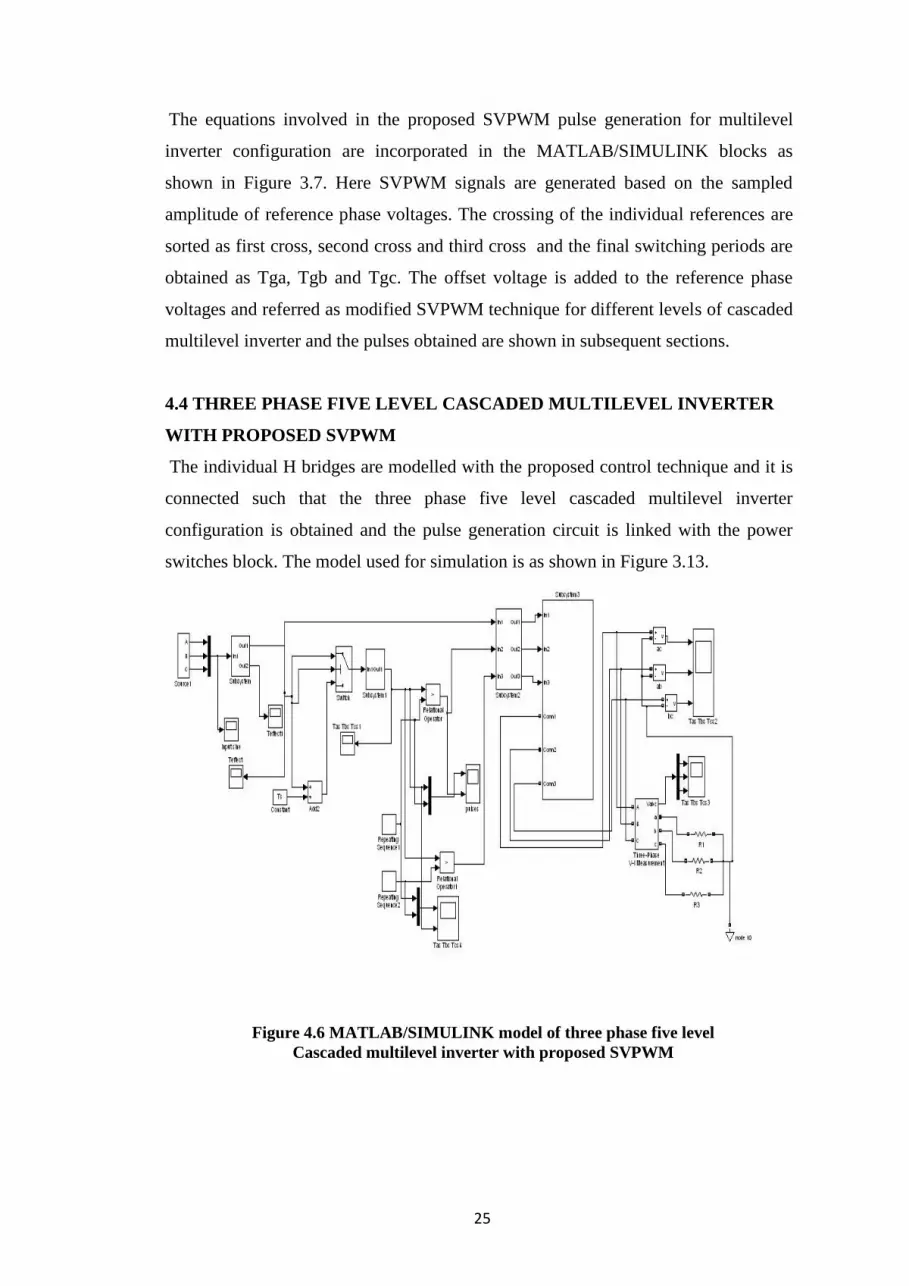
4.4 THREE PHASE FIVE LEVEL CASCADED MULTILEVEL INVERTER
WITH PROPOSED SVPWM
The individual H bridges are modelled with the proposed control technique and it is
connected such that the three phase five level cascaded multilevel inverter
configuration is obtained and the pulse generation circuit is linked with the power
switches block. The model used for simulation is as shown in Figure 3.13.
Figure 4.6 MATLAB/SIMULINK model of three phase five level
Cascaded multilevel inverter with proposed SVPWM

26
4.5 SIMULATION RESULTS
4.5.1 THREE PHASE FIVE LEVEL CMLI WITH PROPOSED SVPWM
The simulation is done for different levels in order to obtain the optimum solution on
the quality of the output waveforms. The same control technique is used to simulate
the different levels with different carrier frequencies irrespective of the levels, 5 kHz
results better performance when compared to other carrier frequencies. Therefore the
same carrier frequency is considered for the simulation irrespective of the levels of
the cascaded configuration.
The offset voltage waveform for the proposed five level cascaded configuration is as
shown in Figure 3.16. Figure 3.17 shows the effective voltage waveforms obtained
from the proposed SVPWM method for the individual phase. The phase sequence is
A, B and C indicated in red, green and blue respectively.
Figure 4.7 OFFSET voltage waveform
Figure 4.8 Effective voltage waveform for five level with four carriers
Time ( Seconds )
M
ag
nit
ud
e
(V)
Time ( Seconds )
M
ag
nit
ud
e
(V)

27
Figure 4.9 the four triangular waveforms and the time equivalents
Figure 4.10 Output phase voltage waveforms
The time equivalents for individual phase voltages are obtained for five level
cascaded multilevel inverter topology. The four reference waveforms are generated
and compared with the sampled phase voltages to obtain the switching pulses for five
level configuration, i.e. (n-1) carrier waveforms as shown in Figure 3.18. The
obtained output phase voltages are as shown in Figure 3.19. The output waveform for
individual phases confirms the constant magnitude over the wide range of operation
and the phase displacements are 1200 apart from each other’s.
Time ( Seconds )
M
ag
nit
ud
e
(V)
Time ( Seconds )
M
ag
nit
ud
e
(V)
28
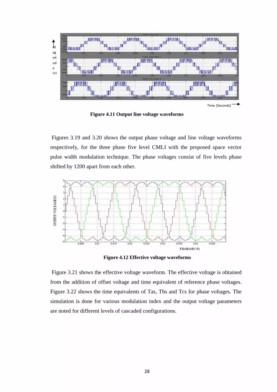
Figures 3.19 and 3.20 shows the output phase voltage and line voltage waveforms
respectively, for the three phase five level CMLI with the proposed space vector
pulse width modulation technique. The phase voltages consist of five levels phase
shifted by 1200 apart from each other.
Figure 4.12 Effective voltage waveforms
Figure 3.21 shows the effective voltage waveform. The effective voltage is obtained
from the addition of offset voltage and time equivalent of reference phase voltages.
Figure 3.22 shows the time equivalents of Tas, Tbs and Tcs for phase voltages. The
simulation is done for various modulation index and the output voltage parameters
are noted for different levels of cascaded configurations.
Figure 4.11 Output line voltage waveforms
Time ( Seconds )
M
ag
nit
ud
e
(V)
29
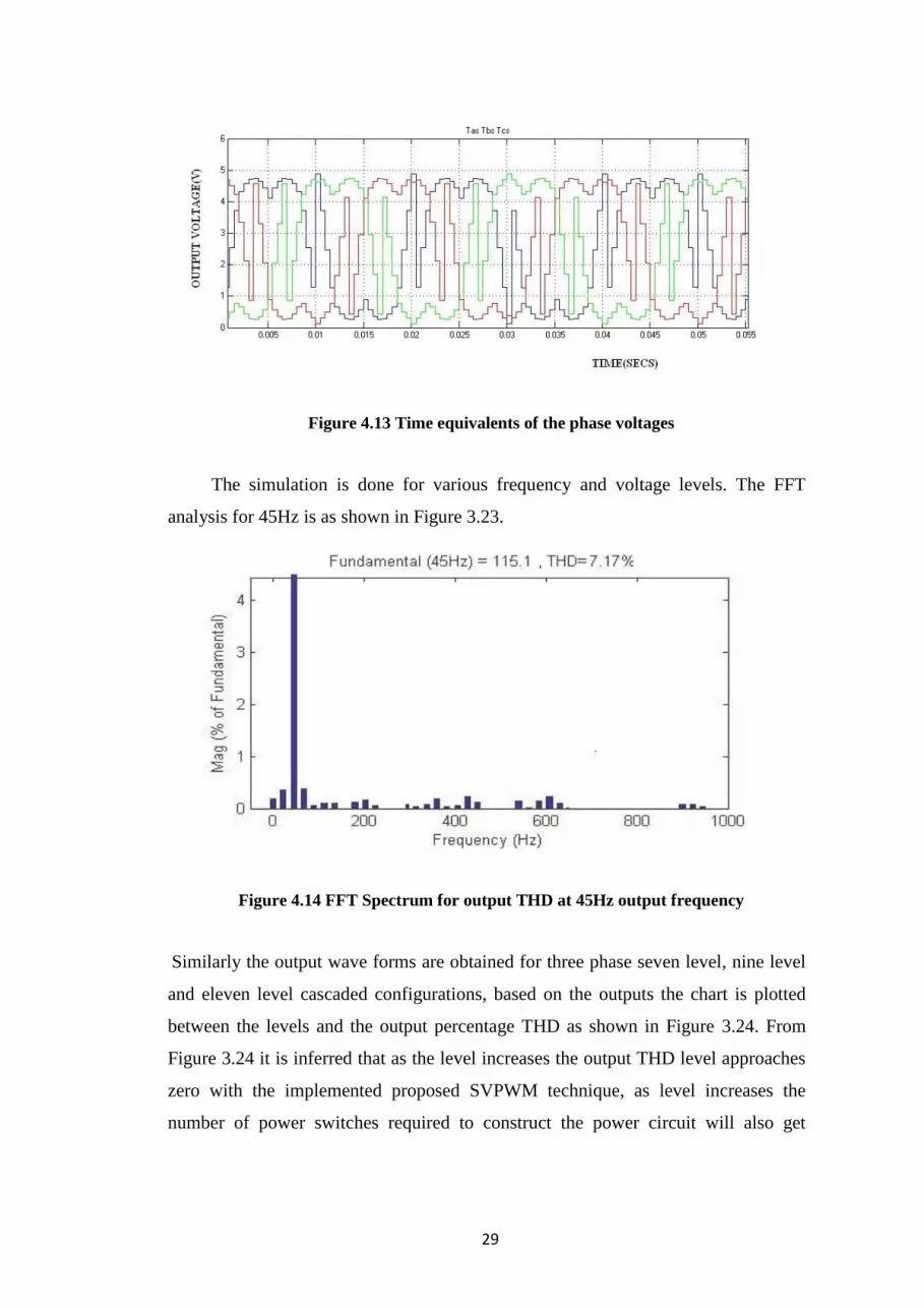
Figure 4.13 Time equivalents of the phase voltages
The simulation is done for various frequency and voltage levels. The FFT
analysis for 45Hz is as shown in Figure 3.23.
Figure 4.14 FFT Spectrum for output THD at 45Hz output frequency
Similarly the output wave forms are obtained for three phase seven level, nine level
and eleven level cascaded configurations, based on the outputs the chart is plotted
between the levels and the output percentage THD as shown in Figure 3.24. From
Figure 3.24 it is inferred that as the level increases the output THD level approaches
zero with the implemented proposed SVPWM technique, as level increases the
number of power switches required to construct the power circuit will also get

30
increased. The control of individual switches will become a complex issue and it is
not an economical solution for the power quality issues.
Figure 4.15 Percentage THD Vs CMLI various levels

31
CHAPTER 5
APPLICATION, ADVANTAGES, DISADVANTAGES & FUTURE SCOPE
5.1 APPLICATIONS
1. DC Power source utilization.
2. Uninterruptable power supplies.
3. Induction heating.
4. HVDC power transmission.
5. Variable frequency drive.
6. Electric vehicle drives.
7. The general case.
5.2 ADVANTAGES
1. Synthesis of higher voltage levels using power devices of lower voltage ratings.
2. Increased number of voltage levels which leads to better voltage waveforms and
reduced total harmonic distortion in output voltage.
3. Reduced switching stresses on the devices due to the reduction of step voltages
between the levels.
4. It not only solves harmonics and EMI problems, but also avoids possible high
frequency switching stress dv/dt.
5. Low switching losses and better electromagnetic compatibility for high power
application.
6. Low power consumption: The consumption of electrical energy can also be
minimized to reduce the total costs associated with the system. This is especially
relevant if it is implemented in a large scale. Each component can be optimized
independently, but the objective relates to the total power consumption.
5.3 DISADVANTAGES
1. The relationship between soil moisture and signal output must be well known or
parameterized. If this relationship varies with the type of soil, it should be known
for the most common soils.
2. The humidity sensors have to be compatible with most soil types.
3. It needs to be durable and resistant to humidity in the long term (5 years).
4. The reading of the probe, when placed permanently in the soil, must be time

32
invariant.
5. Large day-to-day variations make it nearly impossible to maintain constant soil
moisture
5.4 FUTURE SCOPE
A few improvements can be suggested to the next version of the automated irrigation
system:
1. The timing can be defined by the user (e.g. with switch or a keypad and 7-segment
display) instead of being hardwired in the Logic Circuit electronics.
2. The threshold humidity levels may be adjustable using several multi-turn
potentiometers.
3. The use of several moisture probes may be allowed with the addition of a
multiplexing circuit or some kind of mathematical operation (e.g. average).
4. Data logging and/or exporting (e.g. through a RS232 serial port) may be offered.
5. All electronic components may be incorporated on a printed circuit board. They
may also be integrated onto a single chip (so-called System on Chip).
6. A single power supply is desirable to replace the dual (AC/DC) supply of the
prototype. A full-wave rectifier and a voltage regulator should be incorporated on
the PCB to ensure the stability of the 5 V source.
7. Mass production of the controller will reduce the cost of components and
assembly. In addition, scale saving on the probe and valve is likely to be achieved
in mass commercialization.

33
CONCLUSION
The three, five and seven levels of cascaded multi-level inverters are modeled and
simulated using MATLAB/SIMULINK model for different carrier frequencies and
the corresponding values of total harmonic distortion were obtained and analyzed for
magnitude and linearity. The carrier frequency with 5 kHz yields better results in
terms of the output THD and it is fixed for all the levels. From the values of
percentage total harmonic distortion it can be concluded that as the number of levels
of the inverter increases the percentage of the output THD value decreases. As the
number of levels reach infinity, the output percentage of THD approaches zero but
the cost involved in constructing the higher level inverter is high. Since the number
of power switches used to construct the power circuit increases and hence the
complexity in generating the firing pulses for the individual power switches.
Five level inverters have more advantages than the standard two level inverters. AC
link voltage harmonics are lower due to increase in output voltage levels. The
cascaded inverter does not require any voltage balancing capacitors on the input side
and the high voltage fast recovery diodes are not required across the power switches.
Hence the three phase five level cascaded multilevel inverter is considered for
hardware implementation. Hence the output percentage total harmonics distortion is
optimized by the proposed SVPWM technique effectively without any additional
cost on the hardware fabrication. Based on the simulation results obtained a hardware
prototype model of an induction motor drive with a three phase five level cascaded
multilevel inverter is constructed the output parameters are analyzed.
.
34
APPENDIX
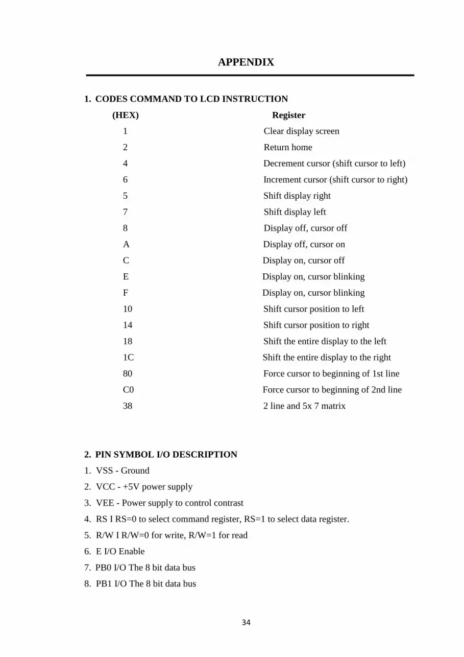
1. CODES COMMAND TO LCD INSTRUCTION
(HEX) Register
1 Clear display screen
2 Return home
4 Decrement cursor (shift cursor to left)
6 Increment cursor (shift cursor to right)
5 Shift display right
7 Shift display left
8 Display off, cursor off
A Display off, cursor on
C Display on, cursor off
E Display on, cursor blinking
F Display on, cursor blinking
10 Shift cursor position to left
14 Shift cursor position to right
18 Shift the entire display to the left
1C Shift the entire display to the right
80 Force cursor to beginning of 1st line
C0 Force cursor to beginning of 2nd line
38 2 line and 5x 7 matrix
2. PIN SYMBOL I/O DESCRIPTION
1. VSS - Ground
2. VCC - +5V power supply
3. VEE - Power supply to control contrast
4. RS I RS=0 to select command register, RS=1 to select data register.
5. R/W I R/W=0 for write, R/W=1 for read
6. E I/O Enable
7. PB0 I/O The 8 bit data bus
8. PB1 I/O The 8 bit data bus

35
9. DB2 I/O The 8 bit data bus
10. DB3 I/O The 8 bit data bus
11. DB4 I/O The 8 bit data bus
12. DB5 I/O The 8 bit data bus
13. DB6 I/O The 8 bit data bus
14. DB7 I/O The 8 bit data bus
3. COMPONENT’S LIST
Voltage Regulator : IC 7805
Op-amp : LM741
Crystal oscillator : 11.0592 M Hz
Diode : IN 4007
LED
Resistor : 470 ohm (for LED),
8.2 K (for power cicuit),
10 K (for sensors),
Potentiometer (100K)
Capacitor : 1000 u f (for Power supply),
10 u f (reset circuit)
33pF (for crystal oscillator)
LCD : 16 x 2
Stepper motor : step angle 7.5 degree, +12V
Relay : 220V/3-4A
Microcontroller : AT89S52
Water pump
Switches
Power cables & ribbon wires

36
REFERENCES
[1]www.ripublication.com/three-phase-inverter-system
[2]www.ijarcsse.com/docs/papers/11.../Volume_2.../V2I10-0158.pdf
[3]www.ijcee.org/papers/471-N032.pdf
[4]www.ijrat.org/downloads/april-2014/paper%20id-24201498.pdf
[5]www.uea.ac.uk/~e680/gmmc/env/env-3a1y/geo/Geo_report_205.pdf
[6]www.eeecube.com/2013/10/inverters.html


