Embed Size (px)
Citation preview
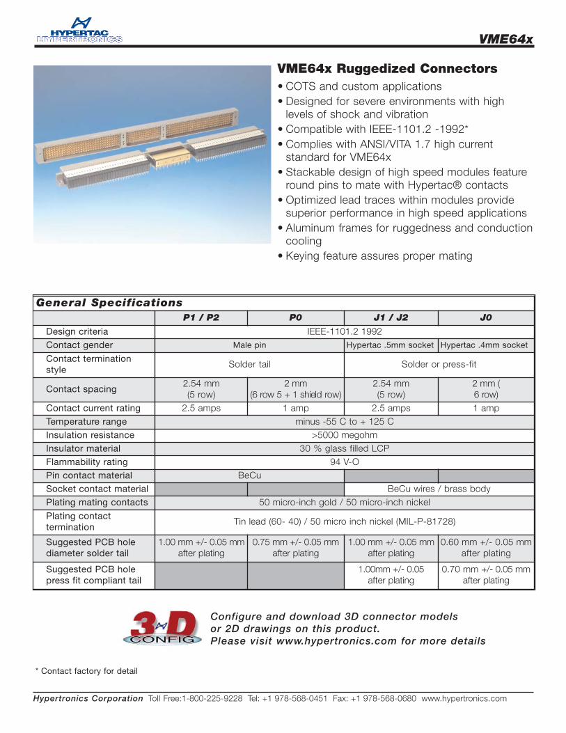
VME64x
Hypertronics Corporation Toll Free:1-800-225-9228 Tel: +1 978-568-0451 Fax: +1 978-568-0680 www.hypertronics.com
VME64x Ruggedized Connectors• COTS and custom applications • Designed for severe environments with high
levels of shock and vibration • Compatible with IEEE-1101.2 -1992*• Complies with ANSI/VITA 1.7 high current
standard for VME64x • Stackable design of high speed modules feature
round pins to mate with Hypertac® contacts • Optimized lead traces within modules provide
superior performance in high speed applications • Aluminum frames for ruggedness and conduction
cooling • Keying feature assures proper mating
Configure and download 3D connector modelsor 2D drawings on this product. Please visit www.hypertronics.com for more details
General SpecificationsP1 / P2 P0 J1 / J2 J0
Design criteria IEEE-1101.2 1992Contact gender Male pin Hypertac .5mm socket Hypertac .4mm socket
Contact terminationstyle
Solder tail Solder or press-fit
Contact spacing2.54 mm (5 row)
2 mm (6 row 5 + 1 shield row)
2.54 mm (5 row)
2 mm (6 row)
Contact current rating 2.5 amps 1 amp 2.5 amps 1 ampTemperature range minus -55 C to + 125 CInsulation resistance >5000 megohmInsulator material 30 % glass filled LCPFlammability rating 94 V-OPin contact material BeCuSocket contact material BeCu wires / brass bodyPlating mating contacts 50 micro-inch gold / 50 micro-inch nickel
Plating contact termination
Tin lead (60- 40) / 50 micro inch nickel (MIL-P-81728)
Suggested PCB hole diameter solder tail
1.00 mm +/- 0.05 mmafter plating
0.75 mm +/- 0.05 mmafter plating
1.00 mm +/- 0.05 mmafter plating
0.60 mm +/- 0.05 mmafter plating
Suggested PCB holepress fit compliant tail
1.00mm +/- 0.05 after plating
0.70 mm +/- 0.05 mmafter plating
* Contact factory for detail
VME64x
Hypertronics Corporation Toll Free:1-800-225-9228 Tel: +1 978-568-0451 Fax: +1 978-568-0680 www.hypertronics.com
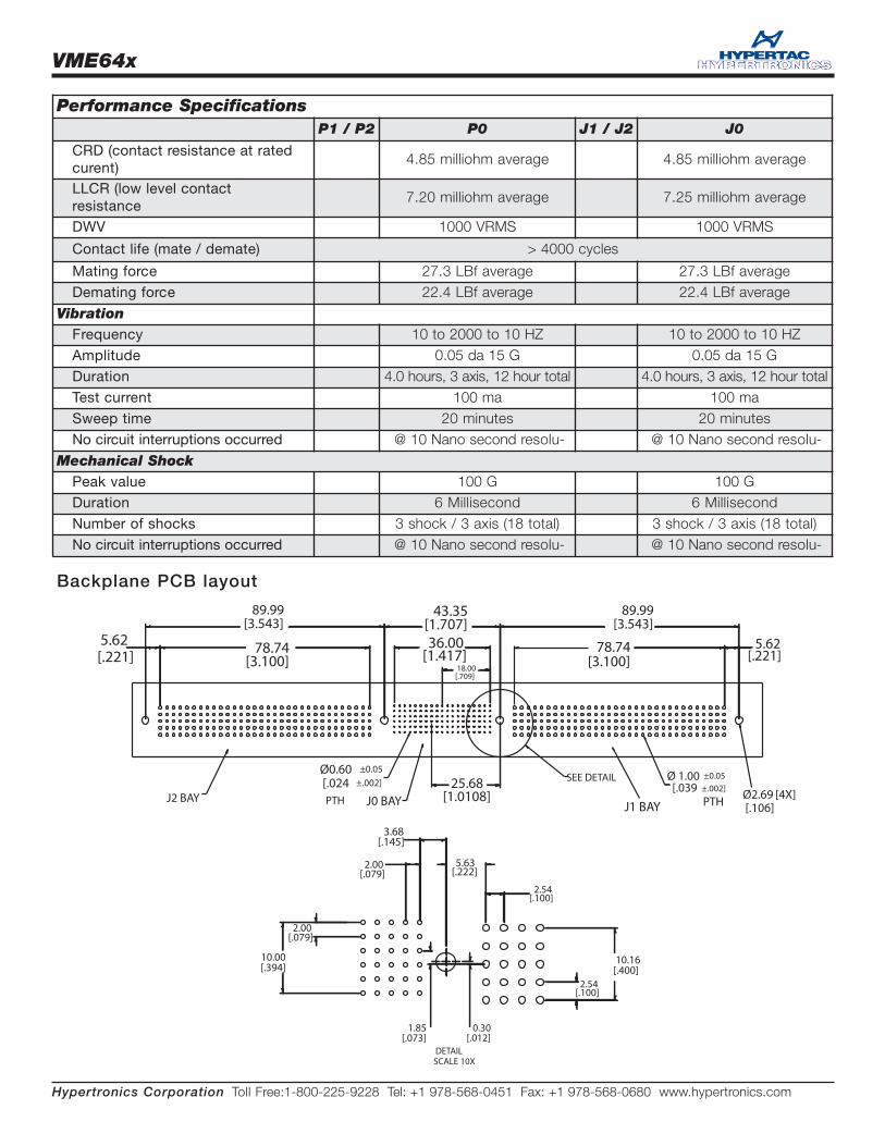
Performance SpecificationsP1 / P2 P0 J1 / J2 J0
CRD (contact resistance at ratedcurent)
4.85 milliohm average 4.85 milliohm average
LLCR (low level contact resistance
7.20 milliohm average 7.25 milliohm average
DWV 1000 VRMS 1000 VRMS
Contact life (mate / demate) > 4000 cycles
Mating force 27.3 LBf average 27.3 LBf averageDemating force 22.4 LBf average 22.4 LBf average
VibrationFrequency 10 to 2000 to 10 HZ 10 to 2000 to 10 HZAmplitude 0.05 da 15 G 0.05 da 15 GDuration 4.0 hours, 3 axis, 12 hour total 4.0 hours, 3 axis, 12 hour totalTest current 100 ma 100 maSweep time 20 minutes 20 minutesNo circuit interruptions occurred @ 10 Nano second resolu- @ 10 Nano second resolu-
Mechanical ShockPeak value 100 G 100 GDuration 6 Millisecond 6 MillisecondNumber of shocks 3 shock / 3 axis (18 total) 3 shock / 3 axis (18 total)No circuit interruptions occurred @ 10 Nano second resolu- @ 10 Nano second resolu-
Backplane PCB layout
VME64x
Hypertronics Corporation Toll Free:1-800-225-9228 Tel: +1 978-568-0451 Fax: +1 978-568-0680 www.hypertronics.com
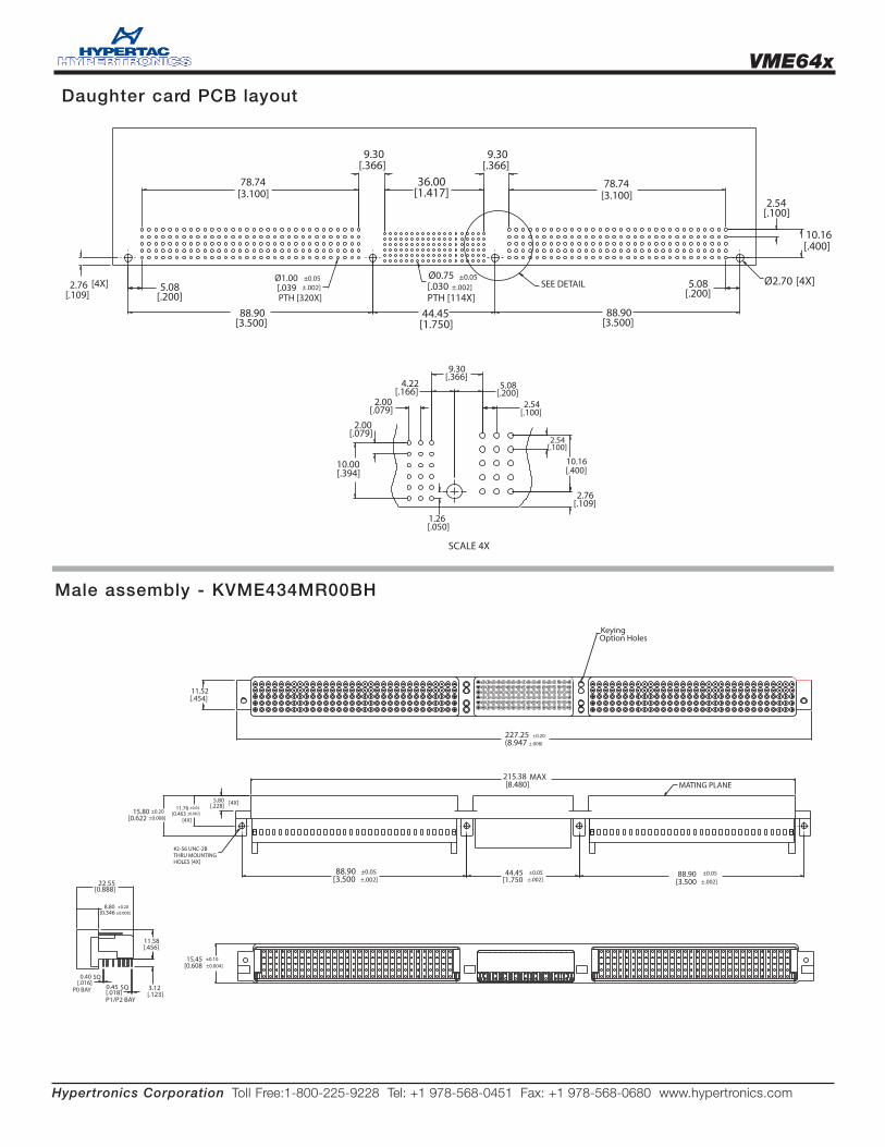
Daughter card PCB layout
Male assembly - KVME434MR00BH
VME64x
Hypertronics Corporation Toll Free:1-800-225-9228 Tel: +1 978-568-0451 Fax: +1 978-568-0680 www.hypertronics.com
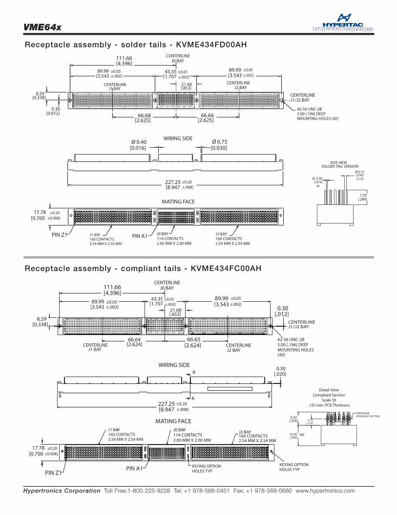
Receptacle assembly - solder tails - KVME434FD00AH
A
Receptacle assembly - compliant tails - KVME434FC00AH
VME64x
Hypertronics Corporation Toll Free:1-800-225-9228 Tel: +1 978-568-0451 Fax: +1 978-568-0680 www.hypertronics.com
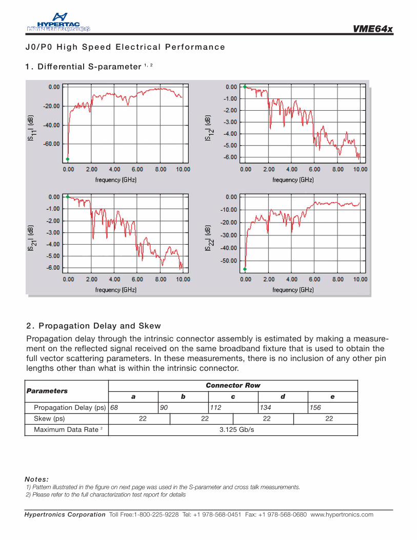
J0/P0 H igh Speed E lec t r i ca l Pe r fo rmance
1 . Differential S-parameter 1, 2
2 . P ropagation Delay and Skew
Propagation delay through the intrinsic connector assembly is estimated by making a measure-ment on the reflected signal received on the same broadband fixture that is used to obtain thefull vector scattering parameters. In these measurements, there is no inclusion of any other pinlengths other than what is within the intrinsic connector.
ParametersConnector Row
a b c d e
Propagation Delay (ps) 68 90 112 134 156
Skew (ps) 22 22 22 22
Maximum Data Rate 2 3.125 Gb/s
Notes:1) Pattern illustrated in the figure on next page was used in the S-parameter and cross talk measurements.2) Please refer to the full characterization test report for details
VME64x
Hypertronics Corporation Toll Free:1-800-225-9228 Tel: +1 978-568-0451 Fax: +1 978-568-0680 www.hypertronics.com
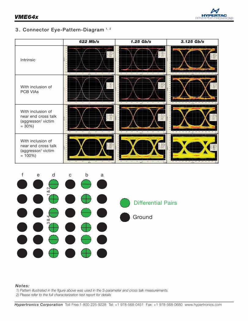
3 . Connector Eye-Pattern-Diagram 1, 2
622 Mb/s 1.25 Gb/s 3.125 Gb/s
Intrinsic
With inclusion of PCB VIAs
With inclusion of near end cross talk(aggressor/ victim = 30%)
With inclusion of near end cross talk(aggressor/ victim = 100%)
f e d c b a
1 &
23
& 4
Differential Pairs
Ground
Notes:1) Pattern illustrated in the figure above was used in the S-parameter and cross talk measurements.2) Please refer to the full characterization test report for details