Embed Size (px)
Citation preview
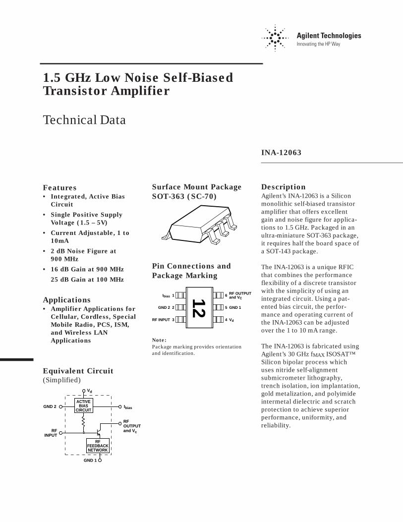
Description
Agilent’s INA-12063 is a Siliconmonolithic self-biased transistoramplifier that offers excellentgain and noise figure for applica-tions to 1.5 GHz. Packaged in anultra-miniature SOT-363 package,it requires half the board space ofa SOT-143 package.
The INA-12063 is a unique RFICthat combines the performanceflexibility of a discrete transistorwith the simplicity of using anintegrated circuit. Using a pat-ented bias circuit, the perfor-mance and operating current ofthe INA-12063 can be adjustedover the 1 to 10 mA range.
The INA-12063 is fabricated usingAgilent’s 30 GHz fMAX ISOSAT™Silicon bipolar process whichuses nitride self-alignmentsubmicrometer lithography,trench isolation, ion implantation,gold metalization, and polyimideintermetal dielectric and scratchprotection to achieve superiorperformance, uniformity, andreliability.
1.5 GHz Low Noise Self-BiasedTransistor Amplifier
Technical Data
INA-12063
Features• Integrated, Active Bias
Circuit
• Single Positive Supply
Voltage (1.5 – 5V)
• Current Adjustable, 1 to
10mA
• 2 dB Noise Figure at
900 MHz
• 16 dB Gain at 900 MHz
25 dB Gain at 100 MHz
Applications
• Amplifier Applications for
Cellular, Cordless, Special
Mobile Radio, PCS, ISM,
and Wireless LAN
Applications
Surface Mount Package
SOT-363 (SC-70)
Pin Connections and
Package Marking
Equivalent Circuit
(Simplified)
Note:
Package marking provides orientationand identification.
RF OUTPUTand VC
GND 1
12
Ibias
GND 2
RF INPUT
1
2
3
6
5
4 Vd
RFINPUT
GND 1
RFOUTPUT and Vc
GND 2
Vd
Ibias
RFFEEDBACKNETWORK
ACTIVEBIAS
CIRCUIT
2
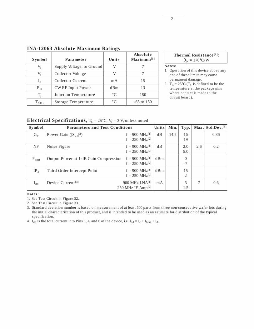
INA-12063 Absolute Maximum Ratings
Absolute
Symbol Parameter Units Maximum[1]
Vd Supply Voltage, to Ground V 7
Vc Collector Voltage V 7
Ic Collector Current mA 15
Pin CW RF Input Power dBm 13
Tj Junction Temperature °C 150
TSTG Storage Temperature °C -65 to 150
Thermal Resistance[2]:
θj-c = 170°C/WNotes:
1. Operation of this device above anyone of these limits may causepermanent damage.
2. TC = 25°C (TC is defined to be thetemperature at the package pinswhere contact is made to thecircuit board).
Electrical Specifications, TC = 25°C, Vd = 3 V, unless noted
Symbol Parameters and Test Conditions Units Min. Typ. Max. Std.Dev.[3]
GP Power Gain (|S21| 2) f = 900 MHz[1] dB 14.5 16 0.36f = 250 MHz[2] 19
NF Noise Figure f = 900 MHz[1] dB 2.0 2.6 0.2f = 250 MHz[2] 5.0
P1dB Output Power at 1 dB Gain Compression f = 900 MHz[1] dBm 0f = 250 MHz[2] -7
IP3 Third Order Intercept Point f = 900 MHz[1] dBm 15f = 250 MHz[2] 2
Idd Device Current[4] 900 MHz LNA[1] mA 5 7 0.6250 MHz IF Amp[2] 1.5
Notes:
1. See Test Circuit in Figure 32.2. See Test Circuit in Figure 33.3. Standard deviation number is based on measurement of at least 500 parts from three non-consecutive wafer lots during
the initial characterization of this product, and is intended to be used as an estimate for distribution of the typicalspecification.
4. Idd is the total current into Pins 1, 4, and 6 of the device, i.e. Idd = Ic + Ibias + Id.
3
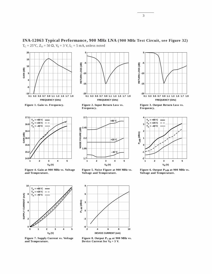
INA-12063 Typical Performance, 900 MHz LNA (900 MHz Test Circuit, see Figure 32)
TC = 25°C, ZO = 50 Ω, Vd = 3 V, IC = 5 mA, unless noted
Vd (V)
Figure 7. Supply Current vs. Voltage
and Temperature.
0
2
4
6
10
8
SU
PP
LY
CU
RR
EN
T (
mA
)
0.1 0.5 0.7 0.9 1.10.3 1.3 1.71.5 1.9
FREQUENCY (GHz)
Figure 1. Gain vs. Frequency.
-10
0
-5
10
5
15
20
GA
IN (
dB
)
1 2 3 4 5
Vd (V)
Figure 4. Gain at 900 MHz vs. Voltage
and Temperature.
14.8
15.6
15.2
16.4
16.0
16.8
17.2
GA
IN (
dB
)
0.1 0.5 0.7 0.9 1.10.3 1.3 1.71.5 1.9
FREQUENCY (GHz)
Figure 2. Input Return Loss vs.
Frequency.
-20
-10
-15
-5
0
RE
TU
RN
LO
SS
(d
B)
0.1 0.5 0.7 0.9 1.10.3 1.3 1.71.5 1.9
FREQUENCY (GHz)
Figure 3. Output Return Loss vs.
Frequency.
-20
-10
-15
-5
0
RE
TU
RN
LO
SS
(d
B)
TA = +85°CTA = +25°CTA = –40°C
TA = +85°CTA = +25°CTA = –40°C
1 2 3 4 5
Vd (V)
Figure 5. Noise Figure at 900 MHz vs.
Voltage and Temperature.
1.7
2.2
1.95
2.45
2.7
NO
ISE
FIG
UR
E (
dB
)
+85°C
+25°C
–40°C
1 2 3 4 5
Vd (V)
Figure 6. Output P1dB at 900 MHz vs.
Voltage and Temperature.
-2
0
-1
2
1
3
4
P1d
B (
dB
m)
TA = +85°CTA = +25°CTA = –40°C
10 2 3 4 5
DEVICE CURRENT (mA)
Figure 8. Output P1 dB at 900 MHz vs.
Device Current for Vd = 3 V.
-6
-3
0
3
9
6
P1
dB
(d
Bm
)
42 6 8 10
4
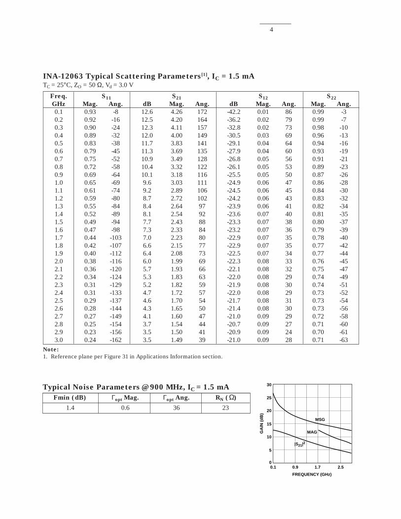
INA-12063 Typical Scattering Parameters[1], IC = 1.5 mATC = 25°C, ZO = 50 Ω, Vd = 3.0 V
Freq. S11 S21 S12 S22
GHz Mag. Ang. dB Mag. Ang. dB Mag. Ang. Mag. Ang.
0.1 0.93 -8 12.6 4.26 172 -42.2 0.01 86 0.99 -30.2 0.92 -16 12.5 4.20 164 -36.2 0.02 79 0.99 -70.3 0.90 -24 12.3 4.11 157 -32.8 0.02 73 0.98 -100.4 0.89 -32 12.0 4.00 149 -30.5 0.03 69 0.96 -130.5 0.83 -38 11.7 3.83 141 -29.1 0.04 64 0.94 -160.6 0.79 -45 11.3 3.69 135 -27.9 0.04 60 0.93 -190.7 0.75 -52 10.9 3.49 128 -26.8 0.05 56 0.91 -210.8 0.72 -58 10.4 3.32 122 -26.1 0.05 53 0.89 -230.9 0.69 -64 10.1 3.18 116 -25.5 0.05 50 0.87 -261.0 0.65 -69 9.6 3.03 111 -24.9 0.06 47 0.86 -281.1 0.61 -74 9.2 2.89 106 -24.5 0.06 45 0.84 -301.2 0.59 -80 8.7 2.72 102 -24.2 0.06 43 0.83 -321.3 0.55 -84 8.4 2.64 97 -23.9 0.06 41 0.82 -341.4 0.52 -89 8.1 2.54 92 -23.6 0.07 40 0.81 -351.5 0.49 -94 7.7 2.43 88 -23.3 0.07 38 0.80 -371.6 0.47 -98 7.3 2.33 84 -23.2 0.07 36 0.79 -391.7 0.44 -103 7.0 2.23 80 -22.9 0.07 35 0.78 -401.8 0.42 -107 6.6 2.15 77 -22.9 0.07 35 0.77 -421.9 0.40 -112 6.4 2.08 73 -22.5 0.07 34 0.77 -442.0 0.38 -116 6.0 1.99 69 -22.3 0.08 33 0.76 -452.1 0.36 -120 5.7 1.93 66 -22.1 0.08 32 0.75 -472.2 0.34 -124 5.3 1.83 63 -22.0 0.08 29 0.74 -492.3 0.31 -129 5.2 1.82 59 -21.9 0.08 30 0.74 -512.4 0.31 -133 4.7 1.72 57 -22.0 0.08 29 0.73 -522.5 0.29 -137 4.6 1.70 54 -21.7 0.08 31 0.73 -542.6 0.28 -144 4.3 1.65 50 -21.4 0.08 30 0.73 -562.7 0.27 -149 4.1 1.60 47 -21.0 0.09 29 0.72 -582.8 0.25 -154 3.7 1.54 44 -20.7 0.09 27 0.71 -602.9 0.23 -156 3.5 1.50 41 -20.9 0.09 24 0.70 -613.0 0.24 -162 3.5 1.49 39 -21.0 0.09 28 0.71 -63
Note:
1. Reference plane per Figure 31 in Applications Information section.
0.1 0.9 1.7 2.5
FREQUENCY (GHz)
0
10
5
20
15
25
30
GA
IN (
dB
)
MAG
MSG
|S21|2
Typical Noise Parameters @ 900 MHz, IC = 1.5 mA
Fmin (dB) Γopt Mag. Γopt Ang. RN (Ω)
1.4 0.6 36 23
5
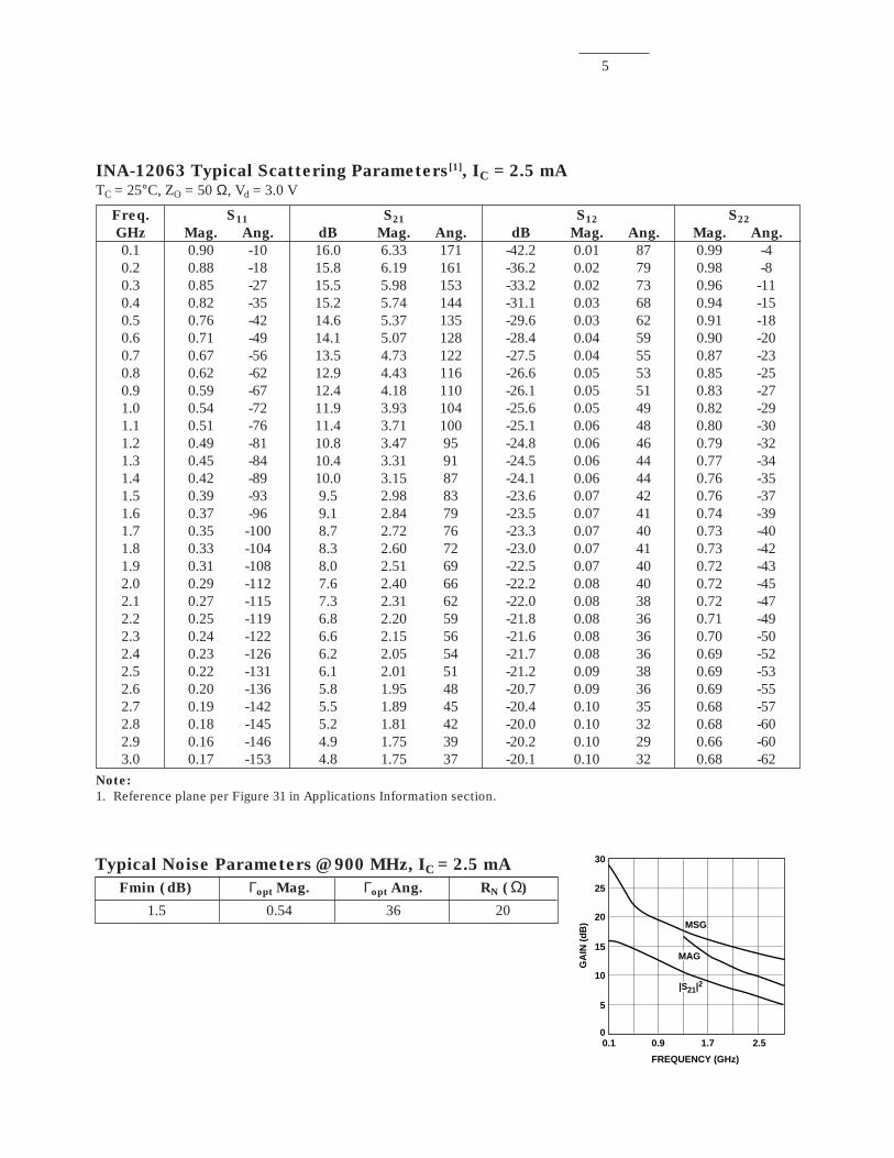
INA-12063 Typical Scattering Parameters[1], IC = 2.5 mATC = 25°C, ZO = 50 Ω, Vd = 3.0 V
Freq. S11 S21 S12 S22
GHz Mag. Ang. dB Mag. Ang. dB Mag. Ang. Mag. Ang.
0.1 0.90 -10 16.0 6.33 171 -42.2 0.01 87 0.99 -40.2 0.88 -18 15.8 6.19 161 -36.2 0.02 79 0.98 -80.3 0.85 -27 15.5 5.98 153 -33.2 0.02 73 0.96 -110.4 0.82 -35 15.2 5.74 144 -31.1 0.03 68 0.94 -150.5 0.76 -42 14.6 5.37 135 -29.6 0.03 62 0.91 -180.6 0.71 -49 14.1 5.07 128 -28.4 0.04 59 0.90 -200.7 0.67 -56 13.5 4.73 122 -27.5 0.04 55 0.87 -230.8 0.62 -62 12.9 4.43 116 -26.6 0.05 53 0.85 -250.9 0.59 -67 12.4 4.18 110 -26.1 0.05 51 0.83 -271.0 0.54 -72 11.9 3.93 104 -25.6 0.05 49 0.82 -291.1 0.51 -76 11.4 3.71 100 -25.1 0.06 48 0.80 -301.2 0.49 -81 10.8 3.47 95 -24.8 0.06 46 0.79 -321.3 0.45 -84 10.4 3.31 91 -24.5 0.06 44 0.77 -341.4 0.42 -89 10.0 3.15 87 -24.1 0.06 44 0.76 -351.5 0.39 -93 9.5 2.98 83 -23.6 0.07 42 0.76 -371.6 0.37 -96 9.1 2.84 79 -23.5 0.07 41 0.74 -391.7 0.35 -100 8.7 2.72 76 -23.3 0.07 40 0.73 -401.8 0.33 -104 8.3 2.60 72 -23.0 0.07 41 0.73 -421.9 0.31 -108 8.0 2.51 69 -22.5 0.07 40 0.72 -432.0 0.29 -112 7.6 2.40 66 -22.2 0.08 40 0.72 -452.1 0.27 -115 7.3 2.31 62 -22.0 0.08 38 0.72 -472.2 0.25 -119 6.8 2.20 59 -21.8 0.08 36 0.71 -492.3 0.24 -122 6.6 2.15 56 -21.6 0.08 36 0.70 -502.4 0.23 -126 6.2 2.05 54 -21.7 0.08 36 0.69 -522.5 0.22 -131 6.1 2.01 51 -21.2 0.09 38 0.69 -532.6 0.20 -136 5.8 1.95 48 -20.7 0.09 36 0.69 -552.7 0.19 -142 5.5 1.89 45 -20.4 0.10 35 0.68 -572.8 0.18 -145 5.2 1.81 42 -20.0 0.10 32 0.68 -602.9 0.16 -146 4.9 1.75 39 -20.2 0.10 29 0.66 -603.0 0.17 -153 4.8 1.75 37 -20.1 0.10 32 0.68 -62
Note:
1. Reference plane per Figure 31 in Applications Information section.
0.1 0.9 1.7 2.5
FREQUENCY (GHz)
0
10
5
20
15
25
30
GA
IN (
dB
)
|S21|2
MSG
MAG
Typical Noise Parameters @ 900 MHz, IC = 2.5 mA
Fmin (dB) Γopt Mag. Γopt Ang. RN (Ω)
1.5 0.54 36 20
6
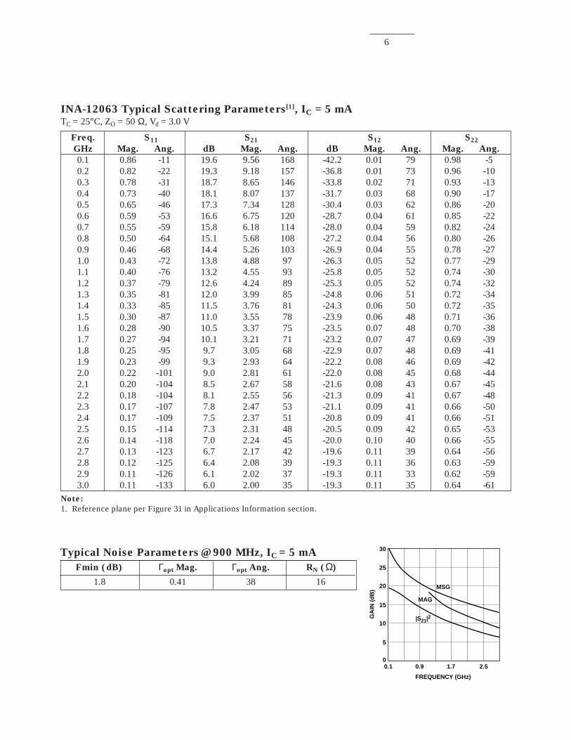
INA-12063 Typical Scattering Parameters[1], IC = 5 mATC = 25°C, ZO = 50 Ω, Vd = 3.0 V
Freq. S11 S21 S12 S22
GHz Mag. Ang. dB Mag. Ang. dB Mag. Ang. Mag. Ang.
0.1 0.86 -11 19.6 9.56 168 -42.2 0.01 79 0.98 -50.2 0.82 -22 19.3 9.18 157 -36.8 0.01 73 0.96 -100.3 0.78 -31 18.7 8.65 146 -33.8 0.02 71 0.93 -130.4 0.73 -40 18.1 8.07 137 -31.7 0.03 68 0.90 -170.5 0.65 -46 17.3 7.34 128 -30.4 0.03 62 0.86 -200.6 0.59 -53 16.6 6.75 120 -28.7 0.04 61 0.85 -220.7 0.55 -59 15.8 6.18 114 -28.0 0.04 59 0.82 -240.8 0.50 -64 15.1 5.68 108 -27.2 0.04 56 0.80 -260.9 0.46 -68 14.4 5.26 103 -26.9 0.04 55 0.78 -271.0 0.43 -72 13.8 4.88 97 -26.3 0.05 52 0.77 -291.1 0.40 -76 13.2 4.55 93 -25.8 0.05 52 0.74 -301.2 0.37 -79 12.6 4.24 89 -25.3 0.05 52 0.74 -321.3 0.35 -81 12.0 3.99 85 -24.8 0.06 51 0.72 -341.4 0.33 -85 11.5 3.76 81 -24.3 0.06 50 0.72 -351.5 0.30 -87 11.0 3.55 78 -23.9 0.06 48 0.71 -361.6 0.28 -90 10.5 3.37 75 -23.5 0.07 48 0.70 -381.7 0.27 -94 10.1 3.21 71 -23.2 0.07 47 0.69 -391.8 0.25 -95 9.7 3.05 68 -22.9 0.07 48 0.69 -411.9 0.23 -99 9.3 2.93 64 -22.2 0.08 46 0.69 -422.0 0.22 -101 9.0 2.81 61 -22.0 0.08 45 0.68 -442.1 0.20 -104 8.5 2.67 58 -21.6 0.08 43 0.67 -452.2 0.18 -104 8.1 2.55 56 -21.3 0.09 41 0.67 -482.3 0.17 -107 7.8 2.47 53 -21.1 0.09 41 0.66 -502.4 0.17 -109 7.5 2.37 51 -20.8 0.09 41 0.66 -512.5 0.15 -114 7.3 2.31 48 -20.5 0.09 42 0.65 -532.6 0.14 -118 7.0 2.24 45 -20.0 0.10 40 0.66 -552.7 0.13 -123 6.7 2.17 42 -19.6 0.11 39 0.64 -562.8 0.12 -125 6.4 2.08 39 -19.3 0.11 36 0.63 -592.9 0.11 -126 6.1 2.02 37 -19.3 0.11 33 0.62 -593.0 0.11 -133 6.0 2.00 35 -19.3 0.11 35 0.64 -61
Note:
1. Reference plane per Figure 31 in Applications Information section.
0.1 0.9 1.7 2.5
FREQUENCY (GHz)
0
10
5
20
15
25
30
GA
IN (
dB
) MSG
|S21|2
MAG
Typical Noise Parameters @ 900 MHz, IC = 5 mA
Fmin (dB) Γopt Mag. Γopt Ang. RN (Ω)
1.8 0.41 38 16
7
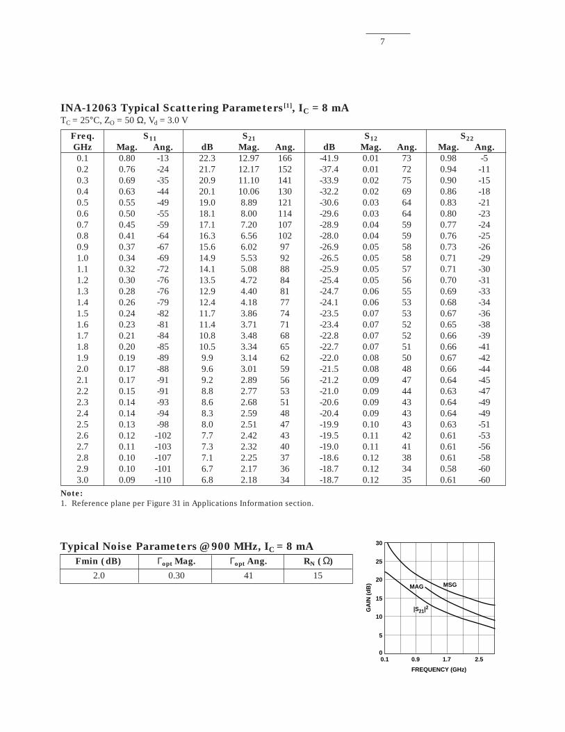
INA-12063 Typical Scattering Parameters[1], IC = 8 mATC = 25°C, ZO = 50 Ω, Vd = 3.0 V
Freq. S11 S21 S12 S22
GHz Mag. Ang. dB Mag. Ang. dB Mag. Ang. Mag. Ang.
0.1 0.80 -13 22.3 12.97 166 -41.9 0.01 73 0.98 -50.2 0.76 -24 21.7 12.17 152 -37.4 0.01 72 0.94 -110.3 0.69 -35 20.9 11.10 141 -33.9 0.02 75 0.90 -150.4 0.63 -44 20.1 10.06 130 -32.2 0.02 69 0.86 -180.5 0.55 -49 19.0 8.89 121 -30.6 0.03 64 0.83 -210.6 0.50 -55 18.1 8.00 114 -29.6 0.03 64 0.80 -230.7 0.45 -59 17.1 7.20 107 -28.9 0.04 59 0.77 -240.8 0.41 -64 16.3 6.56 102 -28.0 0.04 59 0.76 -250.9 0.37 -67 15.6 6.02 97 -26.9 0.05 58 0.73 -261.0 0.34 -69 14.9 5.53 92 -26.5 0.05 58 0.71 -291.1 0.32 -72 14.1 5.08 88 -25.9 0.05 57 0.71 -301.2 0.30 -76 13.5 4.72 84 -25.4 0.05 56 0.70 -311.3 0.28 -76 12.9 4.40 81 -24.7 0.06 55 0.69 -331.4 0.26 -79 12.4 4.18 77 -24.1 0.06 53 0.68 -341.5 0.24 -82 11.7 3.86 74 -23.5 0.07 53 0.67 -361.6 0.23 -81 11.4 3.71 71 -23.4 0.07 52 0.65 -381.7 0.21 -84 10.8 3.48 68 -22.8 0.07 52 0.66 -391.8 0.20 -85 10.5 3.34 65 -22.7 0.07 51 0.66 -411.9 0.19 -89 9.9 3.14 62 -22.0 0.08 50 0.67 -422.0 0.17 -88 9.6 3.01 59 -21.5 0.08 48 0.66 -442.1 0.17 -91 9.2 2.89 56 -21.2 0.09 47 0.64 -452.2 0.15 -91 8.8 2.77 53 -21.0 0.09 44 0.63 -472.3 0.14 -93 8.6 2.68 51 -20.6 0.09 43 0.64 -492.4 0.14 -94 8.3 2.59 48 -20.4 0.09 43 0.64 -492.5 0.13 -98 8.0 2.51 47 -19.9 0.10 43 0.63 -512.6 0.12 -102 7.7 2.42 43 -19.5 0.11 42 0.61 -532.7 0.11 -103 7.3 2.32 40 -19.0 0.11 41 0.61 -562.8 0.10 -107 7.1 2.25 37 -18.6 0.12 38 0.61 -582.9 0.10 -101 6.7 2.17 36 -18.7 0.12 34 0.58 -603.0 0.09 -110 6.8 2.18 34 -18.7 0.12 35 0.61 -60
Note:
1. Reference plane per Figure 31 in Applications Information section.
0.1 0.9 1.7 2.5
FREQUENCY (GHz)
0
10
5
20
15
25
30
GA
IN (
dB
) MAG
|S21|2
MSG
Typical Noise Parameters @ 900 MHz, IC = 8 mA
Fmin (dB) Γopt Mag. Γopt Ang. RN (Ω)
2.0 0.30 41 15
8
INA-12063 Applications
Information
Introduction
The INA-12063 is a unique RFICconfiguration that combines theperformance flexibility of adiscrete transistor with thesimplicity of using an integratedcircuit.
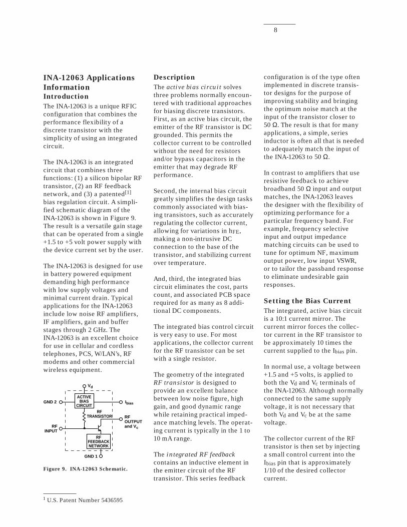
The INA-12063 is an integratedcircuit that combines threefunctions: (1) a silicon bipolar RFtransistor, (2) an RF feedbacknetwork, and (3) a patented[1]
bias regulation circuit. A simpli-fied schematic diagram of theINA-12063 is shown in Figure 9.The result is a versatile gain stagethat can be operated from a single+1.5 to +5 volt power supply withthe device current set by the user.
The INA-12063 is designed for usein battery powered equipmentdemanding high performancewith low supply voltages andminimal current drain. Typicalapplications for the INA-12063include low noise RF amplifiers,IF amplifiers, gain and bufferstages through 2 GHz. TheINA-12063 is an excellent choicefor use in cellular and cordlesstelephones, PCS, W/LAN’s, RFmodems and other commercialwireless equipment.
RFINPUT
GND 1
RFOUTPUT and Vc
GND 2
RFTRANSISTOR
Vd
Ibias
RFFEEDBACKNETWORK
ACTIVEBIAS
CIRCUIT
Figure 9. INA-12063 Schematic.
Description
The active bias circuit solvesthree problems normally encoun-tered with traditional approachesfor biasing discrete transistors.First, as an active bias circuit, theemitter of the RF transistor is DCgrounded. This permits thecollector current to be controlledwithout the need for resistorsand/or bypass capacitors in theemitter that may degrade RFperformance.
Second, the internal bias circuitgreatly simplifies the design taskscommonly associated with bias-ing transistors, such as accuratelyregulating the collector current,allowing for variations in hFE,making a non-intrusive DCconnection to the base of thetransistor, and stabilizing currentover temperature.
And, third, the integrated biascircuit eliminates the cost, partscount, and associated PCB spacerequired for as many as 8 addi-tional DC components.
The integrated bias control circuitis very easy to use. For mostapplications, the collector currentfor the RF transistor can be setwith a single resistor.
The geometry of the integratedRF transistor is designed toprovide an excellent balancebetween low noise figure, highgain, and good dynamic rangewhile retaining practical imped-ance matching levels. The operat-ing current is typically in the 1 to10 mA range.
The integrated RF feedback
contains an inductive element inthe emitter circuit of the RFtransistor. This series feedback
configuration is of the type oftenimplemented in discrete transis-tor designs for the purpose ofimproving stability and bringingthe optimum noise match at theinput of the transistor closer to50 Ω. The result is that for manyapplications, a simple, seriesinductor is often all that is neededto adequately match the input ofthe INA-12063 to 50 Ω.
In contrast to amplifiers that useresistive feedback to achievebroadband 50 Ω input and outputmatches, the INA-12063 leavesthe designer with the flexibility ofoptimizing performance for aparticular frequency band. Forexample, frequency selectiveinput and output impedancematching circuits can be used totune for optimum NF, maximumoutput power, low input VSWR,or to tailor the passband responseto eliminate undesirable gainresponses.
Setting the Bias Current
The integrated, active bias circuitis a 10:1 current mirror. Thecurrent mirror forces the collec-tor current in the RF transistor tobe approximately 10 times thecurrent supplied to the Ibias pin.
In normal use, a voltage between+1.5 and +5 volts, is applied toboth the Vd and Vc terminals ofthe INA-12063. Although normallyconnected to the same supplyvoltage, it is not necessary thatboth Vd and Vc be at the samevoltage.
The collector current of the RFtransistor is then set by injectinga small control current into theIbias pin that is approximately1/10 of the desired collectorcurrent.
1 U.S. Patent Number 5436595
9
The following “10-step” programis suggested as the design se-quence:
1. Determine performance goals.2. Select the bias condition.3. Choose PCB material.4. Check stability.5. Determine required DC
connections.6. Design the input impedance
matching network.7. Design the output impedance
matching network.8. Layout the printed circuit
board.9. Computer optimization and
performance verification.10. Fabricate, assemble, and test.
Each of these steps in the designsequence will now be discussedin the following sections.
Step 1. Establish Performance
Goals
The first step in the design of anINA-12063 amplifier stage is toestablish performance goals. Itmay be necessary to considerperformance tradeoffs betweensome amplifier parameters, suchas Noise Figure, Input VSWR,Gain, Output Power, OutputVSWR, Stability, and DC powerconsumption.
Some of these parameters arecounterposed, for example,increased output power requiresgreater DC power consumption.The tradeoff decisions mayrequire consideration of thechoice of DC bias which isdiscussed in the next section. Thefinal design will often be abalance between system-criticalperformance and those param-eters of lesser significance.
Step 2. Choose Bias
Conditions
The second step of the designprocess is to choose the biasconditions, i.e., the RF transistoroperating voltage (Vc) andcurrent (Ic). The bias conditionsare chosen at this step in thedesign sequence since many ofthe RF design characteristics(e.g., S-parameters and noiseparameters) are dependent oncurrent and/or voltage.
The choice of bias voltage is oftenpreemptive as it is normally fixedby available system resources,such as a battery voltage orsystem power supply. TheINA-12063 will operate fromsupply voltages from 1.5 to5 volts, with +3 volts consideredto be the typical operatingvoltage.
Although noise figure and gainare somewhat insensitive todevice voltage as an independentvariable, some increase in outputpower can be realized with higherdevice voltages.
The bias current has the greatesteffect on RF performance and thefollowing tradeoffs should beconsidered:
Noise Figure increases withdevice current. The data in theTypical Noise Parameter tablesshows an increase in Fmin of from1.4 dB at 1.5 mA of bias current to2.0 dB at 8 mA.
Gain – Transducer gain, |S21|2,increases significantly in propor-tion to device current.
Output Power – One of thebenefits of increased devicecurrent is greater output power. Atypical increase in current from1.5 to 8 mA results in a corre-
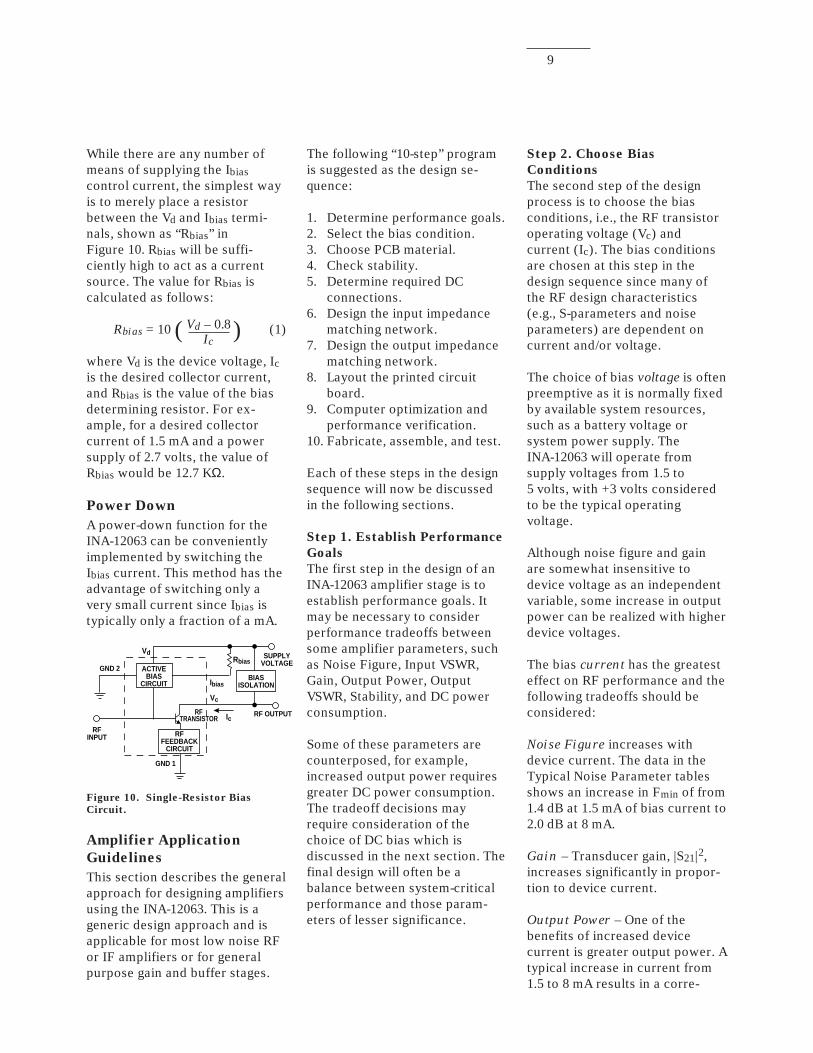
While there are any number ofmeans of supplying the Ibiascontrol current, the simplest wayis to merely place a resistorbetween the Vd and Ibias termi-nals, shown as “Rbias” inFigure 10. Rbias will be suffi-ciently high to act as a currentsource. The value for Rbias iscalculated as follows:
Rbias = 10 ( Vd – 0.8 ) (1) Ic
where Vd is the device voltage, Icis the desired collector current,and Rbias is the value of the biasdetermining resistor. For ex-ample, for a desired collectorcurrent of 1.5 mA and a powersupply of 2.7 volts, the value ofRbias would be 12.7 KΩ.
Power Down
A power-down function for theINA-12063 can be convenientlyimplemented by switching theIbias current. This method has theadvantage of switching only avery small current since Ibias istypically only a fraction of a mA.
RFINPUT
GND 2
Vd
Vc
Ic
Ibias
Rbias
RFTRANSISTOR
GND 1
RF OUTPUT
SUPPLYVOLTAGE
RFFEEDBACK
CIRCUIT
ACTIVEBIAS
CIRCUITBIAS
ISOLATION
Figure 10. Single-Resistor Bias
Circuit.
Amplifier Application
Guidelines
This section describes the generalapproach for designing amplifiersusing the INA-12063. This is ageneric design approach and isapplicable for most low noise RFor IF amplifiers or for generalpurpose gain and buffer stages.
10
sponding increase in P1dB of-5.2 dBm to +4.6 dBm. The datasheet curve in Figure 8 character-izes the P1dB - Ic tradeoff.
Impedance Match – While it isnot a parameter per se, thedegree of difficulty of impedancematch may also be a consider-ation in the selection of biascurrent. Generally, the higher thedevice current, the less “severe”the impedance match, i.e., Γopt,Γms, Γml are all closer to 50 Ω.
Step 3. Selection of PCB
Material
If the selection of PCB materialhas not been preordained byother factors (e.g., system stan-dards) then it should be chosen atthis stage of the design process.The printed circuit board materialis chosen at this step since it willhave an effect on the next step ofthe stability analysis and on thesubsequent design of the imped-ance matching networks.
Key factors to consider in theselection of board material aredielectric constant, RF losscharacteristics, board thickness,and cost.
The dielectric constant and boardthickness together contribute tothe physical geometry of thecircuit, an important consider-ation for miniaturization. Higherdielectric constant materialenables the construction of morecompact circuits since thephysical dimensions of transmis-sion lines are smaller.
In addition to transmission linewidths, PCB board thickness alsoinfluences the quality of groundvias. Ground vias in excessivelythick PCBs result in high induc-tance paths to ground. For someactive devices, poor grounding
can result in performance degra-dation or reduced stability.
Dielectric loss is not a significantfactor for the moderate frequencyranges over which the INA-12063is normally used. Low loss, lowdielectric constant “microwave”type materials are usuallyreserved for applicationsdemanding the very lowest noisefigures (minimum circuit loss)and/or for frequencies above2 GHz.
An overall good choice for mostlow cost wireless applicationsusing devices such as theINA-12063 is a fiberglass-epoxymaterial such as FR-4 or G-10with a thickness in the range of0.020 to 0.031 inches.
Step 4. Stability Analysis
A stability analysis is the nextstep in the design process. Thepurpose of this step is to examinethe circuit’s tendency to oscillate.A linear CAD program, such asAgilent’s Touchstone should beused to calculate the stabilityfactor, K, and stability measure,B1. The factors K and B1 are bothderived from the S-parameters forthe INA-12063 at the previouslyestablished bias voltage andcurrent. The conditions forunconditional stability are:
K > 1 and B1 > 0
While a simple analysis basedonly on the S-parameters is oftenadequate at this point, a slightlymore rigorous analysis is recom-mended that includes the para-sitic elements in the device’s pathto ground. At this stage in thedesign, a reasonable estimation(guess) of this electrical path andthe construction of the groundvias are adequate. For theINA-12063, bear in mind thatPin 5 of the package is the critical
connection for “RF” grounding. Atypical RF path to ground con-sists of a short length of transmis-sion line terminated in one ormore ground vias. (The length ofthe PCB pad between theINA-12063 ground pin and theground should be modeled as amicrostripline (“MLIN” in Touch-
stone), and the plated throughground holes as “VIA” elements.)
When evaluating stability, it is agood practice to calculate K andB1 over the full frequency rangefor which S-parameters areavailable. The reason for this isthat even though K and B1 mayindicate stability over the fre-quency band of interest, thepossibility exists for a circuit tooscillate at frequencies that arefar outside of the band of interest.
While unconditional stabilityrequires a positive, non-zerovalue of B1, most of the followingstability analysis will focus on theK factor since the value of Kindicates the degree of stability.What should the minimum valueof K be to ensure stability? WhileK=1.001 is stable, some margin isprudent to allow for componenttolerances, temperature effects,and manufacturing variations.Typical rules of thumb suggestthat K should be at least 1.2 to1.5.
There are three possible casesresulting from the CAD analysis:
• Case 1 – K>1 over the entirefrequency range.
• Case 2 – K>1 within the bandof interest and K<1 for somefrequencies outside of theband of interest.
• Case 3 – K<1 within the bandof interest.
11
If the CAD analysis indicatesthere is a potential instabilityissue (K < 1 and/or B1 ≤ 0 for anyfrequency) as in Case 2 or Case 3above, then some stabilitycountermeasures will be needed.
There are four basic techniquesfor handling potential instability:
(a) Live with it. If the source andload impedances that will bepresented to the amplifier arewell defined, the finesseapproach of using stability circlesmay be used. Stability circles(calculated by a program such asTouchstone) are plotted on aSmith chart and define regions ofloads that could cause a circuit tooscillate. An amplifier is safefrom oscillation if the expectedamplifier terminations lie welloutside of the unstable regions onboth the input and output imped-ance planes. Since the possibilityof oscillation could exist at anyfrequency for which theINA-12063 has gain, stabilitycircles must be checked atfrequencies over a widefrequency range when thismethod is used.
(b) Resistive feedback. The use ofresistive feedback is often used tocreate stable, wideband, amplifi-ers. While effective in stabilizingactive devices, this method willnot be considered here since asignificant penalty is often paid indegraded NF, less gain, andlowered output powerperformance.
(c) Lossless feedback. Reactivefeedback elements can also beused to stabilize amplifiers. TheINA-12063 already incorporatesone type of reactive feedback inthe emitter of the RF transistor,with a resulting improvement instability. Further use of the
lossless feedback technique is notsuggested for most INA-12063amplifier applications since thismethod adds considerable designcomplexity as well as additionalparts count and board space tothe circuit.
(d) Resistive loading. Resistiveloading can be used at either theinput or output of the INA-12063to create an unconditionallystable amplifier. This is the brute-force method of ensuring stabil-ity. It is fairly fail-safe and is alsothe simplest to implement. Theaddition of a resistive element toeither the amplifier input oroutput creates RF loss whichmanifests itself as lower gain pluseither increased NF (if theresistance is added to the input)or lower output power (if theresistance is placed at theoutput.)
In keeping with the goals of lowcost (i.e., circuit simplicity), theresistive loading method is thetechnique suggested for produc-ing an unconditionally stableamplifier for most applications ofthe INA-12063.
The resistive loading can beapplied in either series or shuntand can be added to either theinput or output of the amplifier.The choice of series or shuntresistive load may be dictated bywhether the real part of theoutput impedance of the amplifierdevice is greater or less than50 Ω. The logical choice is to usea shunt resistor when the ampli-fier impedance is >50 Ω and aseries resistor for the case of>50 Ω. This technique will bringthe overall impedance closer to50 Ω, thus simplifying the match.In some cases, excessive voltagedrop across the stabilizingresistor due to the DC current
into the device may preclude theuse of the series configuration.Shunt resistance is usually themost straightforward solution toimplement since it can be easilybypassed to ground with acapacitor without disturbing thebias.
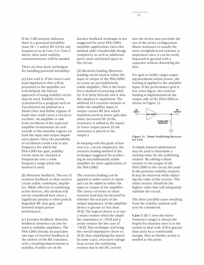
For gain or buffer stages requir-ing maximum output power, theloading is applied to the amplifierinput. If the performance goal islow noise figure, the resistiveloading is implemented on theoutput side of the INA-12063 asshown in Figure 11.
RFINPUT
RFOUTPUT
STABILIZINGRESISTOR
INA-12063
Figure 11. Shunt Stabilizing Resistor
for LNA.
A simple manual optimizationmay be used to determine astarting value for the stabilizingresistor. By adding a shuntresistor to the output of theINA-12063 in the circuit file usedin the previous stability analysis,K may be observed while adjust-ing the value of the resistor. Theshunt resistor should be thehighest value that will adequatelystabilize the circuit.
The three possible cases resultingfrom the stability analysis willnow be considered.
Case 1 (K>1 over the entirefrequency range) is always thehoped for situation since it is theeasiest to deal with. If K is greaterthan unity by a comfortablemargin, then no further action isneeded at this point.
12
Case 2 (K>1 within the band ofinterest; K<1 for some frequen-cies outside of the band ofinterest ) is the next simplest caseto handle. Since K>1 in the bandof interest, little or no perfor-mance tradeoffs may be neededto make the amplifier uncondi-tionally stable.
By using R-C or R-L combina-tions, frequency selective resis-tive loading can be applied onlyover the frequency range forwhich K < 1 in order to stabilizethe amplifier without adverselyaffecting in-band performance.
Case 3 (K<1 in the band of inter-est) requires tradeoffs in NF oroutput power to achieve an uncon-ditionally stable amplifier stage.
The INA-12063 typically falls intoeither Case 2 or Case 3, dependingon the bias current, circuit ground-ing, and frequency band of interest.
In all cases, a final check ofstability should be done in theanalysis of the completed ampli-fier design. This is done as part ofStep 9 in the design sequence.
Step 5. DC Connections
The DC connections to theINA-12063 are considerations inthe next two steps in which theinput and output impedancematching networks are chosen.The goal is economy of compo-nents by integrating as many ofthe DC connections into thematching circuits as practical.For example the use of a series Cin an impedance matchingnetwork could double as a DCblocking capacitor. Or, a shunt Lcan be used to apply the requiredsupply voltage to the output ofthe INA-12063.
One of the advantages of theactive bias circuit in theINA-12063 is that there is no needfor an external DC bias connec-tion to the RF Input. If desired,the input may be connecteddirectly to matching networksusing a series capacitor as thefirst element.
Pins 4 and 6 are connected to thesupply voltage and Pins 2 and 5are DC grounded. Pins 1 and 4should be bypassed to ground. Ahigh value resistor from Pin 1 toPin 6 is a simple and convenientmethod for setting the deviceoperating current. Pin 3, has aninternal voltage present and isnormally connected to a DCblocking capacitor. The only DCconnection which could affect RFperformance is that of applyingthe supply voltage to the RFOutput pin.
Step 6. Designing the Input
Match
The input impedance match isgenerally designed to achieveeither of two goals, either lowestnoise figure or maximum powertransfer. The maximum powertransfer match provides maxi-mum gain and corresponds tominimum VSWR. In some cases,noise circles in combination withconstant gain circles are used todesign an intermediate matchpoint to achieve a compromise inperformance between low noisefigure and low input VSWR.
If the design goal is to obtainlowest NF, the input of theINA-12063 is matched to theconjugate of Γopt. Γopt is thereflection coefficient of thesource termination that results inFmin, the lowest possible devicenoise figure. Γopt design data arefound in the tables of TypicalNoise Parameters. Alternatively
Γopt can be calculated using thesame CAD circuit file used in thestability analysis in Step 4 above.This method is slightly moreaccurate since it takes thefeedback effects of devicegrounding and stabilizationcomponents into account.
If the design goal is to obtainmaximum power transfer (maxi-mum gain/minimum input VSWR),then the input of the INA-12063 ismatched to Γms. Γms is the sourceimpedance resulting from thesimultaneous conjugate match ofthe input and output of thedevice. Since Γms is only definedfor devices/circuits with K > 1,the CAD circuit file from designStep 4, including any stabilizingresistors, is used to calculate Γms.
For most communication systemsoperating over relatively smallbandwidths, a single frequencymatch approach is usuallyadequate. As a general rule, theselection of high pass networksfor the input (and output) match-ing circuits is desirable to reduceexcess gain at low frequencies.
As a final note in the choice of theinput matching structure, the useof a series C element is possibleat the input of the INA-12063since the internal bias circuitobviates the need for an externalDC connection to the input.
The choice of using either lumpedelement or distributed (transmis-sion line) matching elements ismainly dictated by size andfrequency constraints as well asby cost considerations. Whiledistributed elements are “free”since they are etched onto thePCB, they usually use more boardspace than an equivalent lumpedelement (chip) component.
13
Before proceeding to the nextstep, circuit stability and out-of-band gain should be re-checked.
Step 7. Designing the Output
Match
The output of the INA-12063 isnormally matched for maximumpower transfer (maximum gainand lowest output VSWR.)Maximum power transfer occurswhen the output is matched tothe conjugate of Γml. Γml iscomputed from the same CADcircuit file as used for determin-ing Γms in the design of the inputmatching network in the previousstep. A typical LNA is matchedfor Γopt at the input and Γml at theoutput.
Note: The small signal match formaximum power transfer shouldnot be confused with matchingthe output of the INA-12063 forthe highest output power. Asoutput power is increased, thedevice becomes nonlinearresulting in a shift away from theΓml match. While various loadpull types of measurements existto determine the optimumimpedance match for maximumoutput power under nonlinearconditions, these tests are fairlytedious and an empirical tuningapproach is often more expedientto arrive at a solution. The Γmlmatch may be used as a startingpoint in tuning for maximumoutput power.
The same comments regardingsingle frequency match, high passnetworks, and lumped vs. distrib-uted elements referred to in theinput matching step above areapplicable to the output matchingcircuit.
Once again, out-of-band gain andstability should be checked.
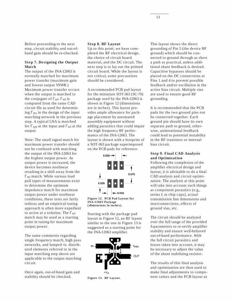
Step 8. RF Layout
Up to this point, we have com-pleted the RF electrical design,the choice of circuit boardmaterial, and the DC circuit. Thenext step is to lay out the printedcircuit board. While the layout isnot critical, some precautionsshould be considered.
A recommended PCB pad layoutfor the miniature SOT-363 (SC-70)package used by the INA-12063 isshown in Figure 12 (dimensionsare in inches). This layout pro-vides ample allowance for pack-age placement by automatedassembly equipment withoutadding parasitics that could impairthe high frequency RF perfor-mance of the INA-12063. Thelayout is shown with a footprint ofa SOT-363 package superimposedon the PCB pads for reference.
0.026
0.035
0.075
0.016
Figure 12. PCB Pad Layout for
INA-12063 Package
(dimensions in inches).
Starting with the package padlayout in Figure 12, an RF layoutsimilar to the one in Figure 13 issuggested as a starting point forthe INA-12063 amplifier.
34
16
Figure 13. RF Layout.
This layout shows the directgrounding of Pin 5 (the device RFground) which should be con-nected to ground through as shorta path as practical, unless addi-tional shunt feedback is desired.Capacitive bypasses should beplaced on the DC connections atPins 1 and 4 to prevent possiblefeedback and/or oscillation in theactive bias circuit. Multiple viasare used to ensure good RFgrounding.
It is recommended that the PCBpads for the two ground pins not
be connected together. Eachground pin should have its ownseparate path to ground, other-wise, unintentional feedbackcould lead to potential instabilityin the RF transistor or internalbias circuit.
Step 9. Final CAD Analysis
and Optimization
Following the completion of theamplifier electrical design andlayout, it is advisable to do a finalCAD analysis and circuit optimi-zation. The analysis at this pointwill take into account such thingsas component parasitics (e.g.,series L in chip caps), actualtransmission line dimensions andinterconnections, effects ofground vias, etc.
The circuit should be analyzedover the full range of the providedS-parameters to re-verify amplifierstability and ensure well-behavedout-of-band performance. Withthe full circuit parasitics andlosses taken into account, it maybe necessary to adjust the valueof the shunt stabilizing resistor.
The results of this final analysisand optimization are then used tomake final adjustments to compo-nent values and the PCB layout as
14
well as to ensure that the perfor-mance goals in Step 1 will be met.
Step 10. Build and Test
The final step is to fabricatecircuit boards and assembleamplifiers for testing and verifica-tion of performance. Someadjustment in component valuesand transmission lines may bedone at this step to allow forimperfections in the computersimulation. This completes theamplifier design.
900 MHz LNA Design Example
As an application example, thedesign of a low noise amplifierstage for 900 MHz using theINA-12063 will be described. Thisamplifier design would be repre-sentative for use in many low-cost, battery power receiverapplications such as LNAs forcellular telephones or 900 MHzISM/spread spectrum systems.
This example will follow theabove design sequence.
1. Performance goals. As areceiver front end stage, theprimary design goals for thisexample amplifier are: (1) noisefigure less than 2 dB, and, (2) ainput 3rd order intercept (IP3)point of at least -10 dBm. Second-ary goals are low output VSWRand minimum DC current drain.The resulting input VSWR andstage gain will be accepted. Lowcost is always a design goal.
Results of this step:
Constrain:
NF ≤ 2 dBInput IP3 ≥ -10 dBmLow cost
Optimize:
Minimize output VSWRMinimize DC power
Accept:
GainInput VSWR
2. Select bias conditions. Forthis example, the supply voltageis constrained by an assumedbattery supply of 3 volts, leavingdevice current as the only remain-ing bias variable. The current isselected based on output powerwhich is driven by the IP3 require-ment. The table of ElectricalSpecifications provides a startingpoint. Using the typical gain of16 dB and a difference of 15 dBbetween the output IP3 and P1dB,the design goal of an input 3rdorder intercept point of -10 dBmis translated to a 1-dB com-pressed output power require-ment of -9 dBm. Figure 8 indi-cates a current of 2.5 mA willmeet this P1dB requirement withadequate design margin.
Results of this step:
Bias: 3 volts, 2.5 mA
3. Choose PCB material. FR-4with a thickness of 0.031 inches ischosen as the printed circuitboard material. FR-4 meets therequirement of low cost whileproviding acceptable low lossperformance at 900 MHz.
A thickness of 0.031 inches issuitable for the miniaturization ofmicrostriplines and thin enoughto allow for low inductanceground vias. With a relativedielectric constant (εr) of 4.8, thewidth of a 50 Ω microstripline on0.031 inch FR-4 is 0.056 inches,which is a convenient size formounting chip components.
Results of this step:
PCB Material: 0.031-inch FR-4
4. Evaluate stability. Stabilityfactor is calculated from the setof S-parameters closest to thechosen bias condition, which inthis example is 3 volts and2.5 mA. For the required accuracyin the stability analysis, a shortlength of transmission line(0.030-inch long, 0.015-inch wide)is added to connect the RFground pin (Pin 5) of theINA-12063 to a 0.025-inch diam-eter ground via.
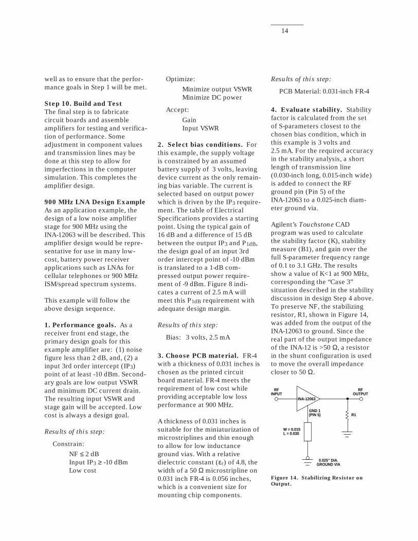
Agilent’s Touchstone CADprogram was used to calculatethe stability factor (K), stabilitymeasure (B1), and gain over thefull S-parameter frequency rangeof 0.1 to 3.1 GHz. The resultsshow a value of K<1 at 900 MHz,corresponding the “Case 3”situation described in the stabilitydiscussion in design Step 4 above.To preserve NF, the stabilizingresistor, R1, shown in Figure 14,was added from the output of theINA-12063 to ground. Since thereal part of the output impedanceof the INA-12 is >50 Ω, a resistorin the shunt configuration is usedto move the overall impedancecloser to 50 Ω.
RFINPUT
W = 0.015L = 0.030
0.025" DIA.GROUND VIA
RFOUTPUT
R1GND 1(PIN 5)
INA-12063
Figure 14. Stabilizing Resistor on
Output.
15
The Touchstone circuit file forthis step is shown in Figure 15.
DIM FREQ GHZ RES OH LNG IN CKT MSUB ER=4.8 H=0.031
T=0.001 RHO=1 RGH=0 S2P 1 2 3 TYP25B.S2P MLIN 3 4 W=0.015 L=0.030 VIA 4 0 D1=0.025
D2=0.025 H=0.031T=0.001
RES 2 0 R=600 ! R1 DEF2P 1 2 INA12 TERM Z0 = 50 OUT INA12 K INA12 B1 INA12 DB[S21] INA12 DB[GMAX] ! INA12 MAG[GMN] ! INA12 ANG[GMN] ! INA12 MAG[GM2] ! INA12 ANG[GM2] FREQ SWEEP 0.1 3.1 0.1
Figure 15. CAD File for Stability
Analysis and Conjugate Match.
The value of the shunt resistor,R1, is varied while observing theresulting K. While a 600 Ω resistoris found to stabilize the circuit at900 MHz (K=1.46), there stillexists a possibility of oscillationat 100 MHz with the worst casevalue of K = 0.72. There are twooptions at this point: (a) lowerthe value of the shunt resistor,which trades additional stabilityfor circuit gain and output power,or (b) use a frequency selectivecircuit to resistive load the deviceonly at lower frequencies.
In the interest of circuit simplicity(meeting the objective of lowcost) the shunt resistor value was
lowered to 290 Ω. This valueresulted in a K > 1 over the fullfrequency range at a trade-off ingain of 1.7 dB. (The stabilitymeasure criteria, B1 > 0, was alsoverified.)
Results of this step:
A 290 Ω shunt resistor was addedto the output of the INA-12063 forstability.
5. Allow for DC connections.
The required DC connections tobe made to this example amplifierare: +3 volts to the RF Outputand Vd terminals (Pins 4 & 6), asuitable bias current into Ibias(Pin 1), and Pins 2 and 5 toground. The RF Input (Pin 3) andRF Output should have blockingcapacitors if the amplifier is to becascaded with stages that do nothave a DC open circuit.
To set the INA-12063 operatingcurrent to 2.5 mA, a 9.1 KΩresistor will be connected be-tween the +3 volt supply and theIbias pin. The DC schematic forthe LNA is shown in Figure 16.
Figure 16. 900 MHz LNA DC
Schematic.
Results of this step:
The DC connections were identi-fied and will be considered inchoosing the input & outputmatching circuits.
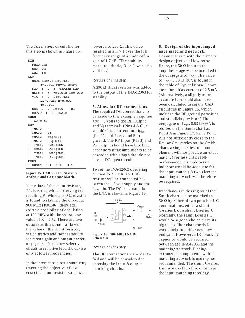
6. Design of the input imped-
ance matching network.
Commensurate with the primarydesign objective of low noisefigure, the 50 Ω input to theamplifier stage will be matched tothe conjugate of Γopt. The valueof Γopt, 0.53 ∠+36°, is found inthe table of Typical Noise Param-eters for a bias current of 2.5 mA.(Alternatively, a slightly moreaccurate Γopt could also havebeen calculated using the CADcircuit file in Figure 15, whichincludes the RF ground parasiticsand stabilizing resistor.) Theconjugate of Γopt, 0.53 ∠−36°, isplotted on the Smith chart asPoint A in Figure 17. Since PointA is not sufficiently close to theR=1 or G=1 circles on the Smithchart, a single series or shuntelement will not provide an exactmatch. (For less critical NFperformance, a simple seriesinductor would be adequate forthe input match.) A two-elementmatching network will thereforebe required.
Impedances in this region of theSmith chart can be matched to50 Ω by either of two possible L-Ccombinations, either a shuntC-series L or a shunt L-series C.Normally, the shunt L-series Cwould be a good choice since itshigh pass filter characteristicwould help roll off excess lowend gain. However, a DC blockingcapacitor would be requiredbetween the INA-12063 and thematching network. Placingextraneous components withinmatching network is usually notrecommended. The shunt C-seriesL network is therefore chosen asthe input matching topology.
16
A
1
C
C (50 Ω) B A (Γopt*)
2
1
-2
B
0.5
0.5
0.2
-0.2
0.2 2
-0.5
-1
RFInput L1 C1
Figure 17. Input Impedance Match.
As shown in Figure 17, a shuntcapacitor of 0.59 pF will moveΓopt * at Point A to a position onthe unit conductance circle (G=1)at Point B. A 11.2 nH seriesinductor then completes thematch to 50 Ω by moving theimpedance at Point B to thecenter of the chart.
The value of the shunt capacitoris small enough that a shortlength of open-circuit transmis-sion line could be used in place ofthe lumped element capacitor.This saves the expense of a chipcomponent with the tradeoff of asmall amount of additional circuitboard space. A 0.20-inch length ofopen-circuit 50 Ω line is onechoice that would be equivalentto the 0.59 pF shunt capacitor.The input matching circuit isshown in Figure 19.
Results of this step:
The input circuit is:
RFINPUT
11.2 nH
0.59 pF
Figure 18. Input Circuit.
7. Design of the output
impedance matching network.
Using the circuit file from step 4(Figure 15), Touchstone was usedto calculate the load impedanceΓml (0.62 ∠+35°) of the INA-12063to achieve maximum powertransfer. The conjugate of Γml,Γml* (0.62 ∠-35°), is plotted asPoint A on the Smith chart inFigure 19.
A
1
C
B
2
1
-2
B
0.5
0.5
0.2
-0.2
0.2 2
-0.5
-1
RFOutputC2L2
C (50 Ω)A (Γml*)
Figure 19. Output Impedance Match.
The two possible L-C networksthat can be used to match Γml* to50 Ω are either a shunt C-series Lor a shunt L-series C circuit. Bychoosing the shunt L-series Ccircuit, two of the DC consider-ations from Step 5 can be satis-fied: the shunt L can be bypassedand used to apply the +3 voltsupply to the RF output terminal,and the series C will serve doubleduty as the DC blocking capacitor.
Referring again to Figure 19, ashunt inductance of 10.8 nHmoves Γml* at Point A to Point Bwhich is on the G1 circle of theSmith chart. The addition of1.9 pF of series capacitancecompletes the impedance trans-formation to Point C at the centerof the chart. The output matchingcircuit is shown in Figure 20.
Results of this step:
The output circuit is:
RFOUTPUT11.2 nH
0.59 pF
Figure 20. Output Circuit.
The circuit values from this stepand from Step 6 will be used as astarting point to be refined inStep 9 when the circuit is ex-panded to take practical intercon-nections and parasitics intoaccount.
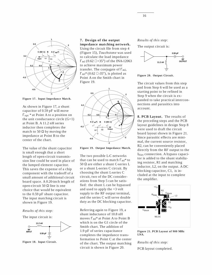
8. PCB Layout. The results ofthe preceding steps and the PCBlayout guidelines in design Step 8were used to draft the circuitboard layout shown in Figure 21.Since parasitic effects are mini-mal, the current source resistor,R2, can be conveniently placeddirectly from the RF output to theIbias connection. A bypass capaci-tor is added to the shunt stabiliz-ing resistor, R1 and matchinginductor, L2, on the output. A DCblocking capacitor, C1, is in-cluded at the input to completethe amplifier.
Figure 21. PCB Layout of 900 MHz
LNA.
Results of this step:
PCB layout completed.
17
9. Final CAD simulation and
optimization. With reference toFigure 21 the CAD circuit filefrom step 4 is embellished toinclude the effects of componentmounting pads, lengths of trans-mission lines used to intercon-nect components, ground vias,bypass and blocking capacitors,etc. (Since 900 MHz is a fairlymoderate frequency, extremelyfine detail is not required.)
Using the previous elementvalues for the matching circuitsas a starting point, Touchstone
was used to optimize the circuitfor noise figure and output match,which were the primary designgoals from Step 1. The input andoutput matching elements wereused as variables for the optimi-zation. Following the optimiza-tion, the value of the stabilizingresistor, R1, was also reviewedand it was found that an increaseto 330 Ω was sufficient to makeK>1 over the entire frequencyrange of the S-parameters. TheTouchstone circuit file for thecomplete amplifier is shown inAppendix A and the simulationresults in Appendix B.
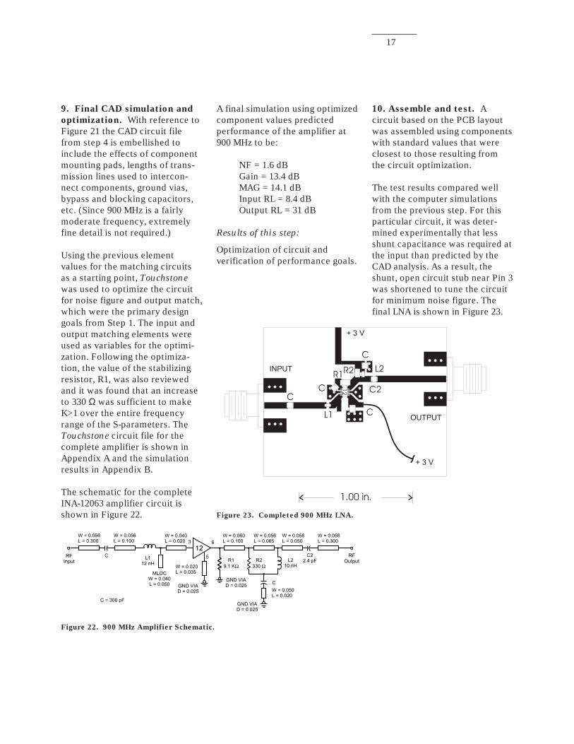
The schematic for the completeINA-12063 amplifier circuit isshown in Figure 22.
A final simulation using optimizedcomponent values predictedperformance of the amplifier at900 MHz to be:
NF = 1.6 dBGain = 13.4 dBMAG = 14.1 dBInput RL = 8.4 dBOutput RL = 31 dB
Results of this step:
Optimization of circuit andverification of performance goals.
10. Assemble and test. Acircuit based on the PCB layoutwas assembled using componentswith standard values that wereclosest to those resulting fromthe circuit optimization.
The test results compared wellwith the computer simulationsfrom the previous step. For thisparticular circuit, it was deter-mined experimentally that lessshunt capacitance was required atthe input than predicted by theCAD analysis. As a result, theshunt, open circuit stub near Pin 3was shortened to tune the circuitfor minimum noise figure. Thefinal LNA is shown in Figure 23.
Figure 22. 900 MHz Amplifier Schematic.
Figure 23. Completed 900 MHz LNA.
18
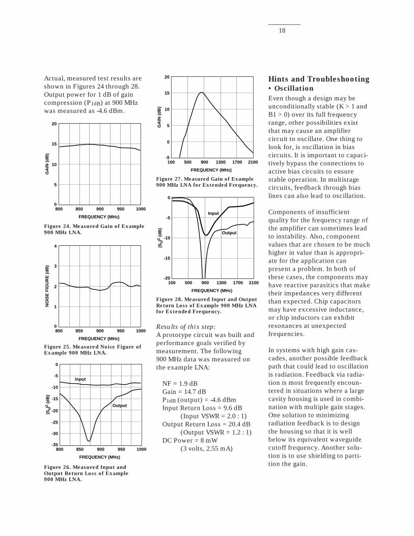
Actual, measured test results areshown in Figures 24 through 28.Output power for 1 dB of gaincompression (P1dB) at 900 MHzwas measured as -4.6 dBm.
FREQUENCY (MHz)
0
5
10
20
15
GA
IN (
dB
)
850800 900 950 1000
Figure 24. Measured Gain of Example
900 MHz LNA.
FREQUENCY (MHz)
0
1
2
4
3
NO
ISE
FIG
UR
E (
dB
)
850800 900 950 1000
Figure 25. Measured Noise Figure of
Example 900 MHz LNA.
FREQUENCY (MHz)
-35
-15
-10
0
-5Input
Output
-30
-25
-20|Sii|
2 (d
B)
850800 900 950 1000
Figure 26. Measured Input and
Output Return Loss of Example
900 MHz LNA.
FREQUENCY (MHz)
-5
5
10
20
15
0
GA
IN (
dB
)500100 900 1300 1700 2100
Figure 27. Measured Gain of Example
900 MHz LNA for Extended Frequency.
FREQUENCY (MHz)
-20
-15
-10
0
-5
|Sii|
2 (d
B)
500100 900 1300 1700 2100
Input
Output
Figure 28. Measured Input and Output
Return Loss of Example 900 MHz LNA
for Extended Frequency.
Results of this step:
A prototype circuit was built andperformance goals verified bymeasurement. The following900 MHz data was measured onthe example LNA:
NF = 1.9 dBGain = 14.7 dBP1dB (output) = -4.6 dBmInput Return Loss = 9.6 dB
(Input VSWR = 2.0 : 1)Output Return Loss = 20.4 dB
(Output VSWR = 1.2 : 1)DC Power = 8 mW
(3 volts, 2.55 mA)
Hints and Troubleshooting
• Oscillation
Even though a design may beunconditionally stable (K > 1 andB1 > 0) over its full frequencyrange, other possibilities existthat may cause an amplifiercircuit to oscillate. One thing tolook for, is oscillation in biascircuits. It is important to capaci-tively bypass the connections toactive bias circuits to ensurestable operation. In multistagecircuits, feedback through biaslines can also lead to oscillation.
Components of insufficientquality for the frequency range ofthe amplifier can sometimes leadto instability. Also, componentvalues that are chosen to be muchhigher in value than is appropri-ate for the application canpresent a problem. In both ofthese cases, the components mayhave reactive parasitics that maketheir impedances very differentthan expected. Chip capacitorsmay have excessive inductance,or chip inductors can exhibitresonances at unexpectedfrequencies.
In systems with high gain cas-cades, another possible feedbackpath that could lead to oscillationis radiation. Feedback via radia-tion is most frequently encoun-tered in situations where a largecavity housing is used in combi-nation with multiple gain stages.One solution to minimizingradiation feedback is to designthe housing so that it is wellbelow its equivalent waveguidecutoff frequency. Another solu-tion is to use shielding to parti-tion the gain.
19
• A Note on Supply Line
Bypassing
When multiple bypass capacitorsare used throughout the powersupply lines in a wireless system,consideration should be given topotential resonances. It is impor-tant to ensure that the capacitors,when combined with additionalparasitic L’s and C’s on the circuitboard, do not form resonantcircuits. The addition of a smallvalue resistor in the bias supplyline between bypass capacitorswill often “de-Q” the bias circuitand eliminate resonance effects.
SMT Assembly
Reliable assembly of surfacemount components is a complexprocess that involves manymaterial, process, and equipmentfactors, including: method ofheating (e.g., IR or vapor phasereflow, wave soldering, etc.)circuit board material, conductorthickness and pattern, type ofsolder alloy, and the thermalconductivity and thermal mass ofcomponents. Components with alow mass, such as the SOT-363package, will reach solder reflowtemperatures faster than thosewith a greater mass.
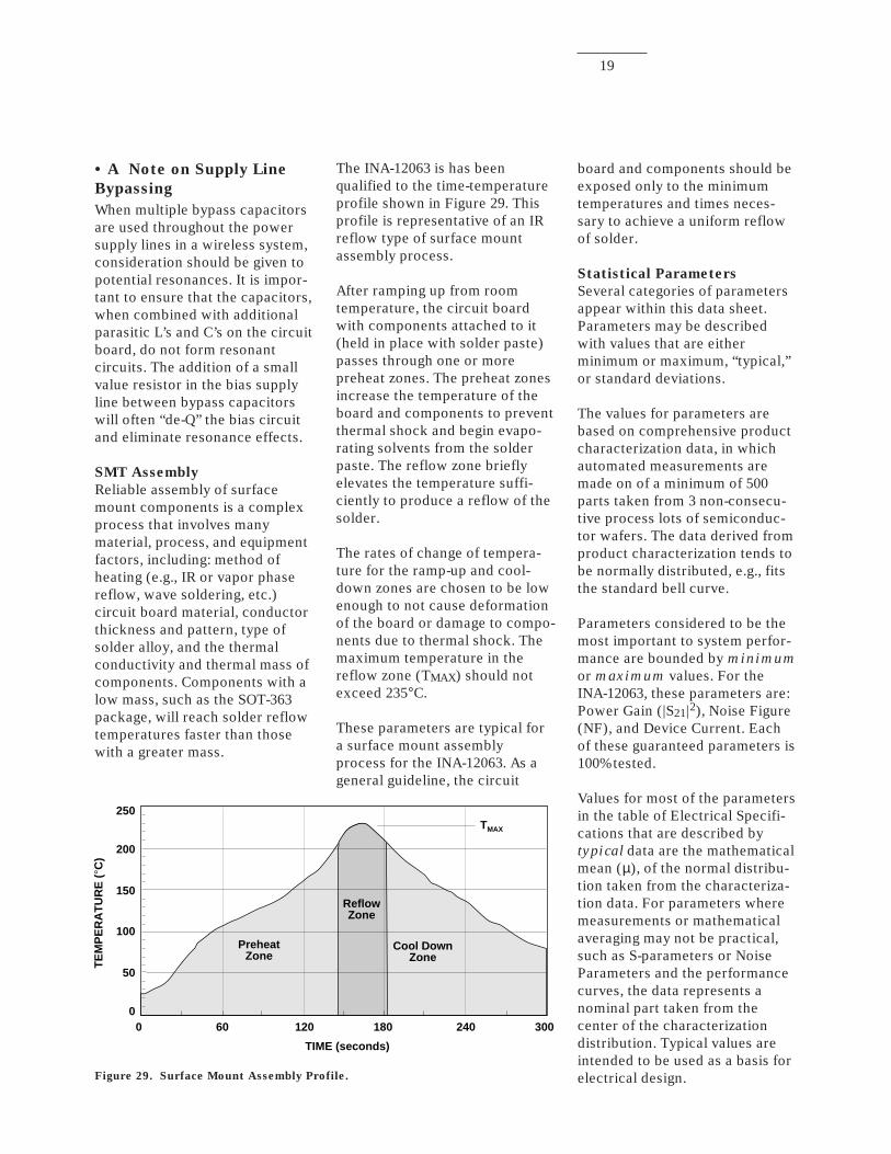
The INA-12063 is has beenqualified to the time-temperatureprofile shown in Figure 29. Thisprofile is representative of an IRreflow type of surface mountassembly process.
After ramping up from roomtemperature, the circuit boardwith components attached to it(held in place with solder paste)passes through one or morepreheat zones. The preheat zonesincrease the temperature of theboard and components to preventthermal shock and begin evapo-rating solvents from the solderpaste. The reflow zone brieflyelevates the temperature suffi-ciently to produce a reflow of thesolder.
The rates of change of tempera-ture for the ramp-up and cool-down zones are chosen to be lowenough to not cause deformationof the board or damage to compo-nents due to thermal shock. Themaximum temperature in thereflow zone (TMAX) should notexceed 235°C.
These parameters are typical fora surface mount assemblyprocess for the INA-12063. As ageneral guideline, the circuit
board and components should beexposed only to the minimumtemperatures and times neces-sary to achieve a uniform reflowof solder.
Statistical Parameters
Several categories of parametersappear within this data sheet.Parameters may be describedwith values that are eitherminimum or maximum, “typical,”or standard deviations.
The values for parameters arebased on comprehensive productcharacterization data, in whichautomated measurements aremade on of a minimum of 500parts taken from 3 non-consecu-tive process lots of semiconduc-tor wafers. The data derived fromproduct characterization tends tobe normally distributed, e.g., fitsthe standard bell curve.
Parameters considered to be themost important to system perfor-mance are bounded by minimum
or maximum values. For theINA-12063, these parameters are:Power Gain (|S21|2), Noise Figure(NF), and Device Current. Eachof these guaranteed parameters is100% tested.
Values for most of the parametersin the table of Electrical Specifi-cations that are described bytypical data are the mathematicalmean (µ), of the normal distribu-tion taken from the characteriza-tion data. For parameters wheremeasurements or mathematicalaveraging may not be practical,such as S-parameters or NoiseParameters and the performancecurves, the data represents anominal part taken from thecenter of the characterizationdistribution. Typical values areintended to be used as a basis forelectrical design.
TIME (seconds)
TMAX
TE
MP
ER
AT
UR
E (
°C)
00
50
100
150
200
250
60
PreheatZone
Cool DownZone
ReflowZone
120 180 240 300
Figure 29. Surface Mount Assembly Profile.
20
To assist designers in optimizingnot only the immediate circuitusing the INA-12063, but to alsooptimize and evaluate trade-offsthat affect a complete wirelesssystem, the standard deviation
(σ) is provided for many of theElectrical Specifications param-eters (at 25°C) in addition to themean. The standard deviation is ameasure of the variability aboutthe mean. It will be recalled that anormal distribution is completelydescribed by the mean andstandard deviation.
Standard statistics tables orcalculations provide the probabil-ity of a parameter falling betweenany two values, usually symmetri-cally located about the mean.Referring to Figure 30 for ex-ample, the probability of aparameter being between ±1σ is68.3%; between ±2σ is 95.4%; andbetween ±3σ is 99.7%.
68%
95%
99%
Parameter Value
Mean (µ), typ
-3σ -2σ -1σ +1σ +2σ +3σ
Figure 30. Normal Distribution.
Phase Reference Planes
The positions of the referenceplanes used to specify S-param-eters and Noise Parameters forthe INA-12063 are shown inFigure 31. As seen in the illustra-tion, the reference planes arelocated at the point where thepackage leads contact the testcircuit.
TEST CIRCUIT
REFERENCEPLANES
Figure 31. Phase Reference Planes.
Test Circuits
The test circuit shown in Fig-ure 32 is used for 100% testing ofthe guaranteed RF and DCparameters that are shown in theTable of Electrical Specifications.
RFINPUT
RFOUTPUT
8.2 nH
5.6 kΩ
10 nF 100 pF
8.2 nH500 Ω
1 nF
1 nF
2.2 pF
+3 V
+3 V
+3 V
12
Figure 32. 900 MHz Test Circuit.
The test circuits in Figures 32 and33 were used to generate thecharacterization data and perfor-mance curves for 900 MHz and250 MHz.
RFINPUT
RFOUTPUT
180 nH
150 Ω
5.6 pF
16 kΩ
10 nF 100 pF
39 nH330 Ω
1 nF
1 nF
5.6 pF
+3 V
+3 V
+3 V
12
Figure 33. 250 MHz Test Circuit.
Electrostatic Sensitivity
RFICs are electro-static discharge(ESD) sensitivedevices. Although theINA-12063 is robust in design,permanent damage may occur tothese devices if they are sub-jected to high energy electrostatic
discharges. Electrostatic chargesas high as several thousand volts(which readily accumulate on thehuman body and on test equip-ment) can discharge withoutdetection and may result indegradation in performance,reliability, or failure.
Electronic devices may besubjected to ESD damage in anyof the following areas:
• Storage and handling• Inspection and testing• Assembly• In-circuit use
The INA-12063 is a ESD Class 1device. Therefore, proper ESDprecautions are recommendedwhen handling, inspecting,testing, assembling, and usingthese devices to avoid damage.
The in-use aspect of potentialESD damage is sometimes over-looked. One such example ofpossible damage is in the use ofan ESD sensitive device as thefront-end LNA stage in personalcommunication equipment, suchas cellular telephones, PCS, or RFmodems.
The input to receiver LNAs arefrequently connected to externalantennas that are subject tohuman contact and exposure toother potentially damaging levelsof ESD. If this type of conditionexists, some type of circuitprotection may be needed. Onesimple method of preventing ESDdamage is to add a DC returnpath (e.g., a shunt inductor) tothe input of the receiver. Thistype of protection may be inte-grated into other parts of thereceiver front end, such as in aT/R switch, filter, or the inputmatching network to the LNA.
21
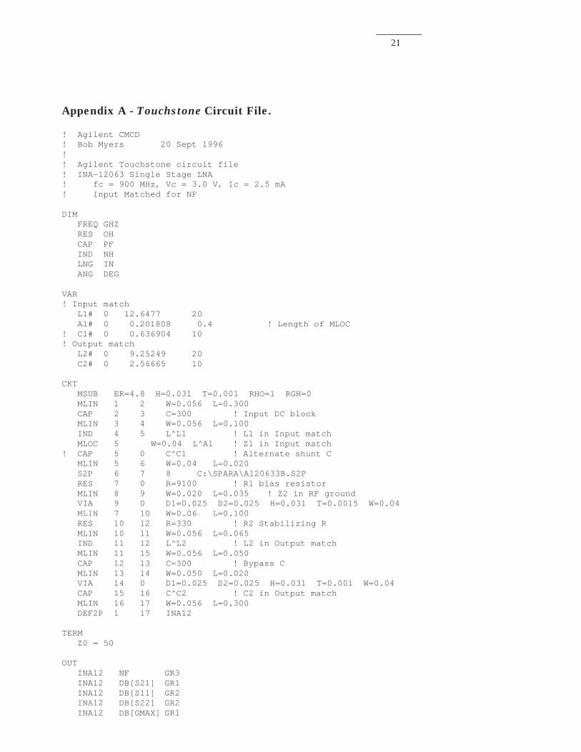
Appendix A - Touchstone Circuit File.
! Agilent CMCD! Bob Myers 20 Sept 1996!! Agilent Touchstone circuit file! INA-12063 Single Stage LNA! fc = 900 MHz, Vc = 3.0 V, Ic = 2.5 mA! Input Matched for NF
DIM FREQ GHZ RES OH CAP PF IND NH LNG IN ANG DEG
VAR! Input match L1# 0 12.6477 20 A1# 0 0.201808 0.4 ! Length of MLOC! C1# 0 0.636904 10! Output match L2# 0 9.25249 20 C2# 0 2.56665 10
CKT MSUB ER=4.8 H=0.031 T=0.001 RHO=1 RGH=0 MLIN 1 2 W=0.056 L=0.300 CAP 2 3 C=300 ! Input DC block MLIN 3 4 W=0.056 L=0.100 IND 4 5 L^L1 ! L1 in Input match MLOC 5 W=0.04 L^A1 ! Z1 in Input match! CAP 5 0 C^C1 ! Alternate shunt C MLIN 5 6 W=0.04 L=0.020 S2P 6 7 8 C:\SPARA\A120633B.S2P RES 7 0 R=9100 ! R1 bias resistor MLIN 8 9 W=0.020 L=0.035 ! Z2 in RF ground VIA 9 0 D1=0.025 D2=0.025 H=0.031 T=0.0015 W=0.04 MLIN 7 10 W=0.06 L=0.100 RES 10 12 R=330 ! R2 Stabilizing R MLIN 10 11 W=0.056 L=0.065 IND 11 12 L^L2 ! L2 in Output match MLIN 11 15 W=0.056 L=0.050 CAP 12 13 C=300 ! Bypass C MLIN 13 14 W=0.050 L=0.020 VIA 14 0 D1=0.025 D2=0.025 H=0.031 T=0.001 W=0.04 CAP 15 16 C^C2 ! C2 in Output match MLIN 16 17 W=0.056 L=0.300 DEF2P 1 17 INA12
TERM Z0 = 50
OUT INA12 NF GR3 INA12 DB[S21] GR1 INA12 DB[S11] GR2 INA12 DB[S22] GR2 INA12 DB[GMAX] GR1
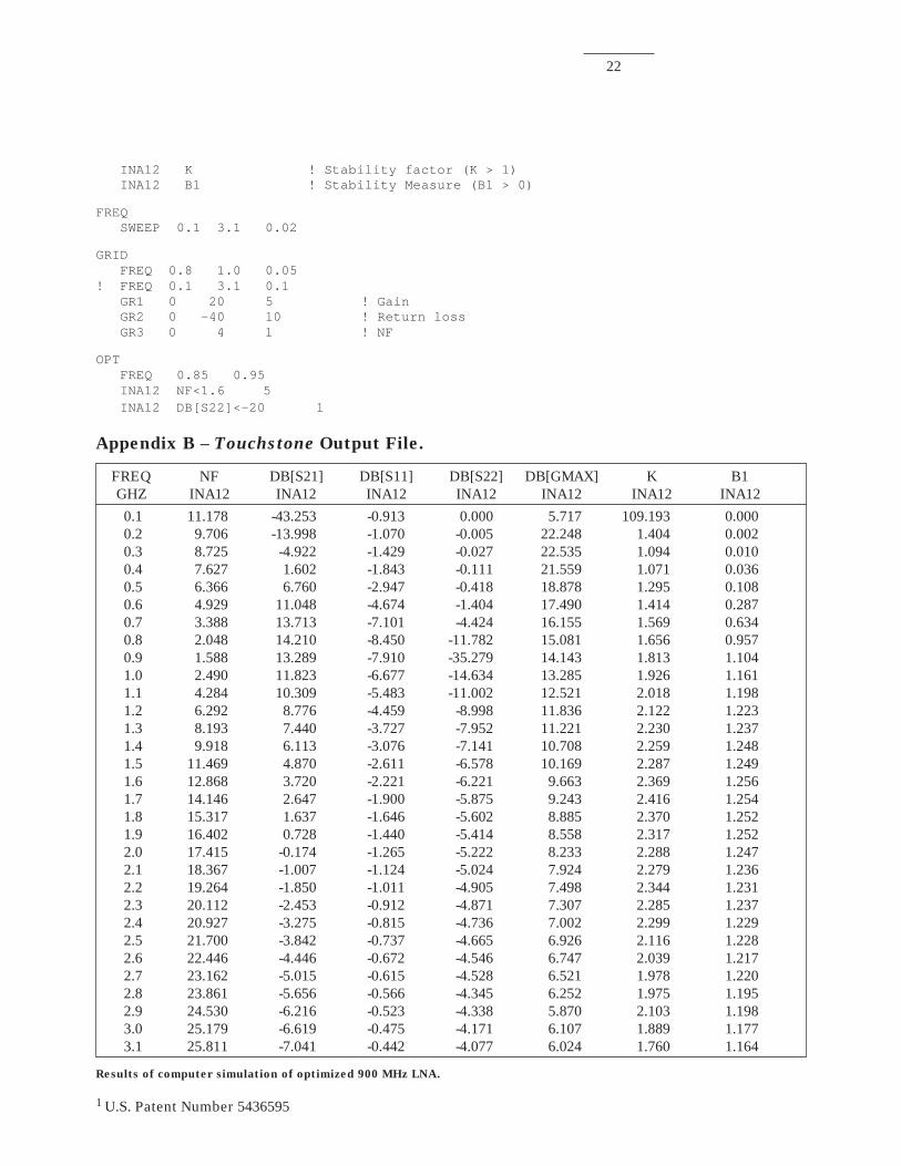
22
INA12 K ! Stability factor (K > 1) INA12 B1 ! Stability Measure (B1 > 0)
FREQ SWEEP 0.1 3.1 0.02
GRID FREQ 0.8 1.0 0.05! FREQ 0.1 3.1 0.1 GR1 0 20 5 ! Gain GR2 0 -40 10 ! Return loss GR3 0 4 1 ! NF
OPT FREQ 0.85 0.95 INA12 NF<1.6 5 INA12 DB[S22]<-20 1
Appendix B – Touchstone Output File.
FREQ NF DB[S21] DB[S11] DB[S22] DB[GMAX] K B1GHZ INA12 INA12 INA12 INA12 INA12 INA12 INA12
0.1 11.178 -43.253 -0.913 0.000 5.717 109.193 0.0000.2 9.706 -13.998 -1.070 -0.005 22.248 1.404 0.0020.3 8.725 -4.922 -1.429 -0.027 22.535 1.094 0.0100.4 7.627 1.602 -1.843 -0.111 21.559 1.071 0.0360.5 6.366 6.760 -2.947 -0.418 18.878 1.295 0.1080.6 4.929 11.048 -4.674 -1.404 17.490 1.414 0.2870.7 3.388 13.713 -7.101 -4.424 16.155 1.569 0.6340.8 2.048 14.210 -8.450 -11.782 15.081 1.656 0.9570.9 1.588 13.289 -7.910 -35.279 14.143 1.813 1.1041.0 2.490 11.823 -6.677 -14.634 13.285 1.926 1.1611.1 4.284 10.309 -5.483 -11.002 12.521 2.018 1.1981.2 6.292 8.776 -4.459 -8.998 11.836 2.122 1.2231.3 8.193 7.440 -3.727 -7.952 11.221 2.230 1.2371.4 9.918 6.113 -3.076 -7.141 10.708 2.259 1.2481.5 11.469 4.870 -2.611 -6.578 10.169 2.287 1.2491.6 12.868 3.720 -2.221 -6.221 9.663 2.369 1.2561.7 14.146 2.647 -1.900 -5.875 9.243 2.416 1.2541.8 15.317 1.637 -1.646 -5.602 8.885 2.370 1.2521.9 16.402 0.728 -1.440 -5.414 8.558 2.317 1.2522.0 17.415 -0.174 -1.265 -5.222 8.233 2.288 1.2472.1 18.367 -1.007 -1.124 -5.024 7.924 2.279 1.2362.2 19.264 -1.850 -1.011 -4.905 7.498 2.344 1.2312.3 20.112 -2.453 -0.912 -4.871 7.307 2.285 1.2372.4 20.927 -3.275 -0.815 -4.736 7.002 2.299 1.2292.5 21.700 -3.842 -0.737 -4.665 6.926 2.116 1.2282.6 22.446 -4.446 -0.672 -4.546 6.747 2.039 1.2172.7 23.162 -5.015 -0.615 -4.528 6.521 1.978 1.2202.8 23.861 -5.656 -0.566 -4.345 6.252 1.975 1.1952.9 24.530 -6.216 -0.523 -4.338 5.870 2.103 1.1983.0 25.179 -6.619 -0.475 -4.171 6.107 1.889 1.1773.1 25.811 -7.041 -0.442 -4.077 6.024 1.760 1.164
Results of computer simulation of optimized 900 MHz LNA.
1 U.S. Patent Number 5436595
23
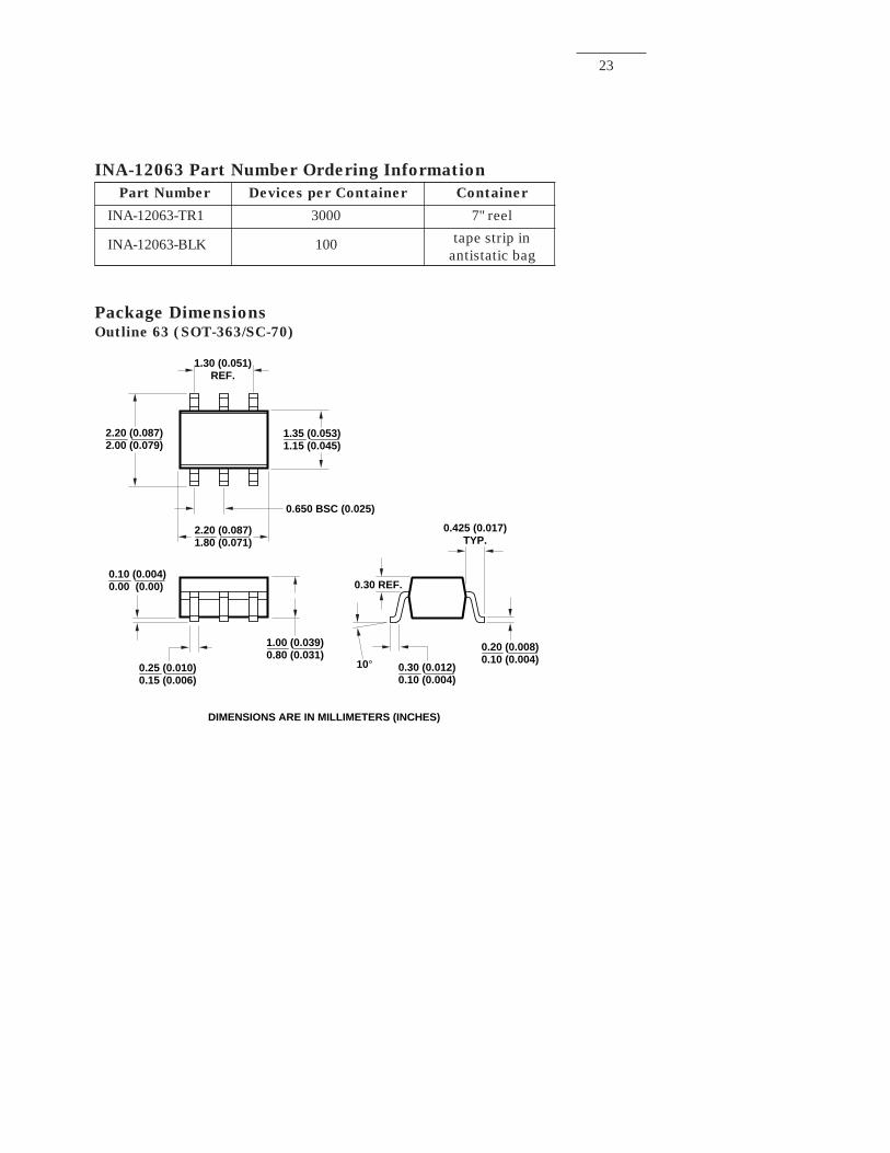
INA-12063 Part Number Ordering Information
Part Number Devices per Container Container
INA-12063-TR1 3000 7" reel
INA-12063-BLK 100 tape strip inantistatic bag
Package DimensionsOutline 63 (SOT-363/SC-70)
2.20 (0.087)2.00 (0.079)
1.35 (0.053)1.15 (0.045)
1.30 (0.051)REF.
0.650 BSC (0.025)
2.20 (0.087)1.80 (0.071)
0.10 (0.004)0.00 (0.00)
0.25 (0.010)0.15 (0.006)
1.00 (0.039)0.80 (0.031)
0.20 (0.008)0.10 (0.004)
0.30 (0.012)0.10 (0.004)
0.30 REF.
10°
0.425 (0.017)TYP.
DIMENSIONS ARE IN MILLIMETERS (INCHES)
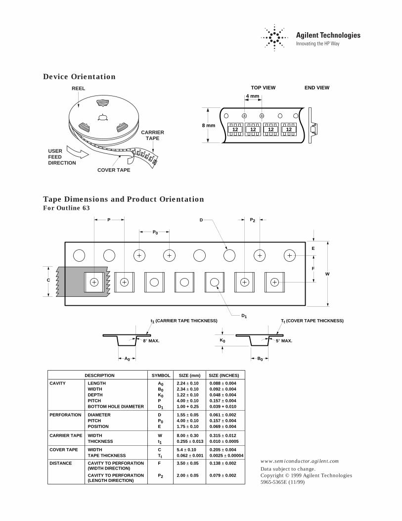
Tape Dimensions and Product OrientationFor Outline 63
Device Orientation
USERFEED DIRECTION
COVER TAPE
CARRIERTAPE
REEL END VIEW
8 mm
4 mm
TOP VIEW
12 12 12 12
P
P0
P2
FW
C
D1
D
E
A0
8° MAX.
t1 (CARRIER TAPE THICKNESS) Tt (COVER TAPE THICKNESS)
5° MAX.
B0
K0
DESCRIPTION SYMBOL SIZE (mm) SIZE (INCHES)
LENGTHWIDTHDEPTHPITCHBOTTOM HOLE DIAMETER
A0B0K0PD1
2.24 ± 0.102.34 ± 0.101.22 ± 0.104.00 ± 0.101.00 + 0.25
0.088 ± 0.0040.092 ± 0.0040.048 ± 0.0040.157 ± 0.0040.039 + 0.010
CAVITY
DIAMETERPITCHPOSITION
DP0E
1.55 ± 0.054.00 ± 0.101.75 ± 0.10
0.061 ± 0.0020.157 ± 0.0040.069 ± 0.004
PERFORATION
WIDTHTHICKNESS
Wt1
8.00 ± 0.300.255 ± 0.013
0.315 ± 0.0120.010 ± 0.0005
CARRIER TAPE
CAVITY TO PERFORATION(WIDTH DIRECTION)
CAVITY TO PERFORATION(LENGTH DIRECTION)
F
P2
3.50 ± 0.05
2.00 ± 0.05
0.138 ± 0.002
0.079 ± 0.002
DISTANCE
WIDTHTAPE THICKNESS
CTt
5.4 ± 0.100.062 ± 0.001
0.205 ± 0.0040.0025 ± 0.00004
COVER TAPE
www.semiconductor.agilent.com
Data subject to change.Copyright © 1999 Agilent Technologies5965-5365E (11/99)


![RF Circuit Design - [Ch4-1] Microwave Transistor Amplifier](https://img.pdfslide.net/doc/110x75/55cc6094bb61eb9d338b474f/rf-circuit-design-ch4-1-microwave-transistor-amplifier.jpg)