Embed Size (px)
Citation preview
55:035 Computer Architecture and Organization
Lecture 11
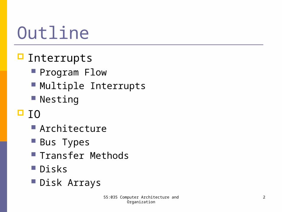
Outline Interrupts
Program Flow Multiple Interrupts Nesting
IO Architecture Bus Types Transfer Methods Disks Disk Arrays
255:035 Computer Architecture and Organization

Interrupts Mechanism by which other modules (e.g. I/O) may
interrupt normal sequence of processing Program
e.g. overflow, division by zero
Timer Generated by internal processor timer Used in pre-emptive multi-tasking
I/O from I/O controller
Hardware failure e.g. memory parity error
355:035 Computer Architecture and Organization

Interrupt Cycle Added to instruction cycle Processor checks for interrupt
Indicated by an interrupt signal
If no interrupt, fetch next instruction If interrupt pending:
Suspend execution of current program Save context Set PC to start address of interrupt handler routine Process interrupt Restore context and continue interrupted program
4
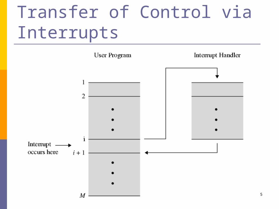
Transfer of Control via Interrupts
5

Program Flow Control
6

Program Timing Short I/O Wait
7
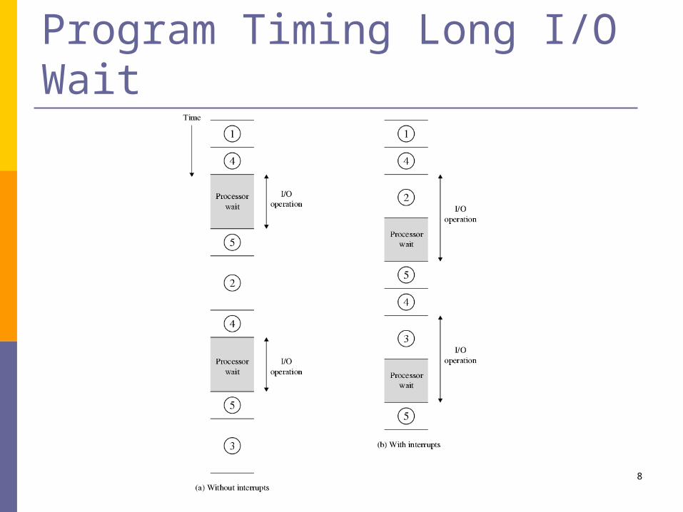
Program Timing Long I/O Wait
8
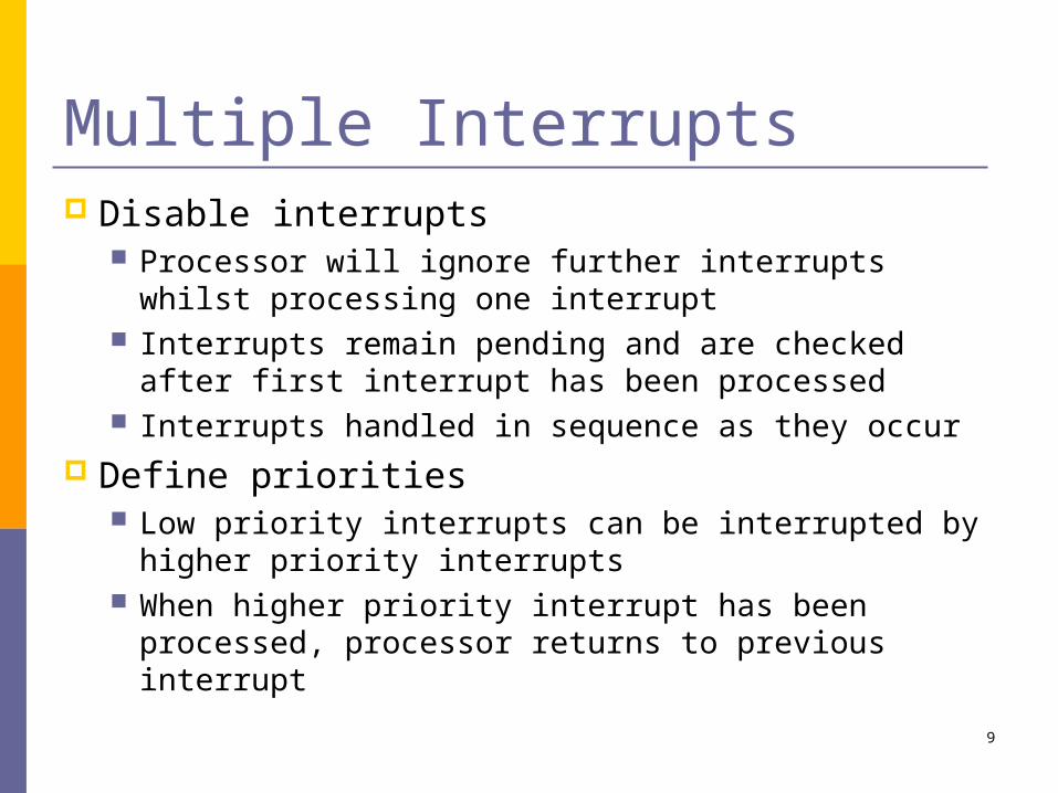
Multiple Interrupts Disable interrupts
Processor will ignore further interrupts whilst processing one interrupt
Interrupts remain pending and are checked after first interrupt has been processed
Interrupts handled in sequence as they occur
Define priorities Low priority interrupts can be interrupted by higher
priority interrupts When higher priority interrupt has been processed,
processor returns to previous interrupt9
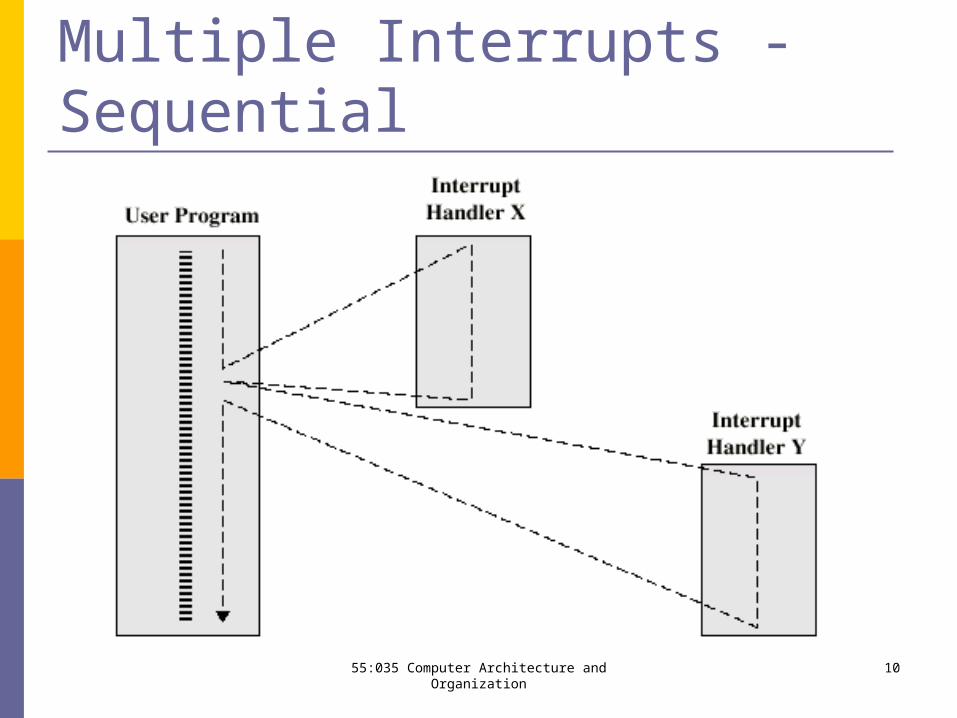
Multiple Interrupts - Sequential
1055:035 Computer Architecture and Organization
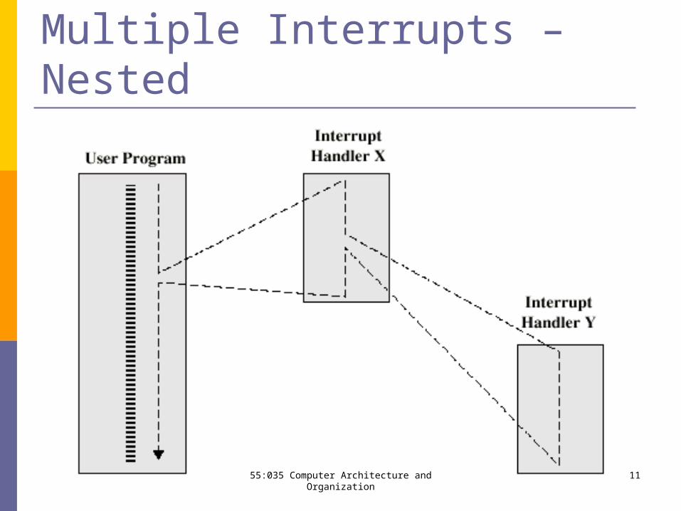
Multiple Interrupts – Nested
1155:035 Computer Architecture and Organization

Time Sequence of Multiple Interrupts
1255:035 Computer Architecture and Organization

Input/Output & System Performance IssuesInput/Output & System Performance Issues System Architecture & I/O Connection StructureSystem Architecture & I/O Connection Structure
Types of Buses/Interconnects in the system.Types of Buses/Interconnects in the system.
I/O Data Transfer Methods.I/O Data Transfer Methods. Cache & I/O: Cache & I/O: The Stale Data Problem I/O Performance Metrics.I/O Performance Metrics. Magnetic Disk Characteristics.Magnetic Disk Characteristics. Designing an I/O System & System Performance:Designing an I/O System & System Performance:
Determining system performance bottleneck.Determining system performance bottleneck. ((which component creates a system performance bottleneck)
1355:035 Computer Architecture and Organization

The Von-Neumann Computer ModelThe Von-Neumann Computer Model Partitioning of the computing engine into components:
Central Processing Unit (CPU): Control Unit (instruction decode, sequencing of operations), Datapath (registers, arithmetic and logic unit, buses).
Memory: Instruction (program) and operand (data) storage.
Input/Output (I/O): Communication between the CPU and the outside world
-Memory
(instructions, data)
Control
DatapathregistersALU, buses
CPUComputer System
Input
Output
I/O Devices
I/O Subsystem
System performance depends on many aspects of the system (“limited by weakest link in the chain”) 14

Input and Output (I/O) Subsystem The I/O subsystem provides the mechanism for
communication between the CPU and the outside world (I/O devices).
Design factors: I/O device characteristics (input, output, storage, etc.). I/O Connection Structure (degree of separation from memory
operations). I/O interface (the utilization of dedicated I/O and bus controllers). Types of buses (processor-memory vs. I/O buses). I/O data transfer or synchronization method (programmed I/O,
interrupt-driven, DMA).
1555:035 Computer Architecture and Organization

Typical System ArchitectureTypical System Architecture
I/O Controller Hub(Chipset South Bridge)
System Bus or Front Side Bus (FSB)
Memory Controller(Chipset North Bridge)
I/O Subsystem
Isolated I/O
16

System ComponentsSystem Components
SDRAMPC100/PC133100-133MHz64-128 bits wide2-way inteleaved~ 900 MBYTES/SEC )64bit)
Double DateRate (DDR) SDRAMPC3200200 MHz DDR64-128 bits wide4-way interleaved~3.2 GBYTES/SEC (64bit)
RAMbus DRAM (RDRAM)400MHZ DDR16 bits wide (32 banks)~ 1.6 GBYTES/SEC
CPU
Caches
System Bus
I/O Devices
Memory
I/O Controllers
Bus Adapter
DisksDisplaysKeyboards
Networks
NICs
Main I/O BusMemoryController Example: PCI, 33-66MHz
32-64 bits wide 133-528 MB/sPCI-X 133MHz 64-bits wide 1066 MB/s
L1
L2 L3
Memory Bus
NorthBridge
SouthBridge
Chipset
I/O Subsystem
(FSB)
Important issue: Which component creates a system performance bottleneck?
(possiblyon-chip)
Chipset
Time(workload) = Time(CPU) + Time(I/O) - Time(Overlap)
1755:035 Computer Architecture and Organization

I/O InterfaceI/O InterfaceI/O Interface, I/O controller or I/O bus adapter:
Specific to each type of I/O device. To the CPU, and I/O device, it consists of a set of control and data
registers (usually memory-mapped) within the I/O address space. On the I/O device side, it forms a localized I/O bus which can be shared
by several I/O devices (e.g IDE, SCSI, USB ...)
Handles I/O details (originally done by CPU) such as:
Assembling bits into words, Low-level error detection and correction Accepting or providing words in word-sized I/O registers. Presents a uniform interface to the CPU regardless of I/O
device.
Processingoff-loaded from CPU
1855:035 Computer Architecture and Organization

I/O Controller ArchitectureI/O Controller Architecture
Peripheral or Main I/O Bus (PCI, PCI-X, etc.)
HostMemory
ProcessorCache
HostProcessor
Peripheral Bus Interface/DMA
I/O Channel Interface
BufferMemory
ROM
µProc
I/O Controller
ChipsetSouth Bridge
ChipsetNorth Bridge
Micro-controllerorEmbedded processor
SCSI, IDE, USB, ….19

Types of Buses in The System Types of Buses in The System (1/2)(1/2) Processor-Memory Bus System Bus, Front Side Bus, (FSB)
Should offer very high-speed (bandwidth) and low latency. Matched to the memory system performance to maximize memory-
processor bandwidth. Usually design-specific (not an industry standard). Examples:
Alpha EV6 (AMD K7), Peak bandwidth = 400 MHz x 8 = 3.2 GB/s Intel GTL+ (P3), Peak bandwidth = 133 MHz x 8 = 1 GB/s Intel P4, Peak bandwidth = 800 Mhz x 8 = 6.4 GB/s HyperTransport 2.0: 200Mhz-1.4GHz, Peak bandwidth up to
22.8 GB/s (point-to-point system interconnect not a bus)
20

Types of Buses in The System Types of Buses in The System (2/2)(2/2) I/O buses (sometimes called an interface):
Follow bus industry standards. Usually formed by I/O interface adapters to handle
many types of connected I/O devices. Wide range in the data bandwidth and latency Not usually interfaced directly to memory instead
connected processor-memory bus via a bus adapter (chipset south bridge).
Examples: Main system I/O bus: PCI, PCI-X, PCI Express Storage: SATA, IDE, SCSI.
2155:035 Computer Architecture and Organization

Intel Pentium 4 System Architecture (Using The Intel 925 Chipset)
CPU(Including cache) System Bus (Front Side Bus, FSB)
Bandwidth usually should match or exceedthat of main memory
I/O Controller Hub(Chipset South Bridge)
SystemMemoryTwo 8-byte DDR2 Channels
Main I/O Bus(PCI)
Graphics I/O Bus (PCI Express)
Memory Controller Hub(Chipset North Bridge)
Misc.I/OInterfaces
Misc.I/OInterfaces
Storage I/O (Serial ATA)
I/O Subsystem2255:035 Computer Architecture and Organization
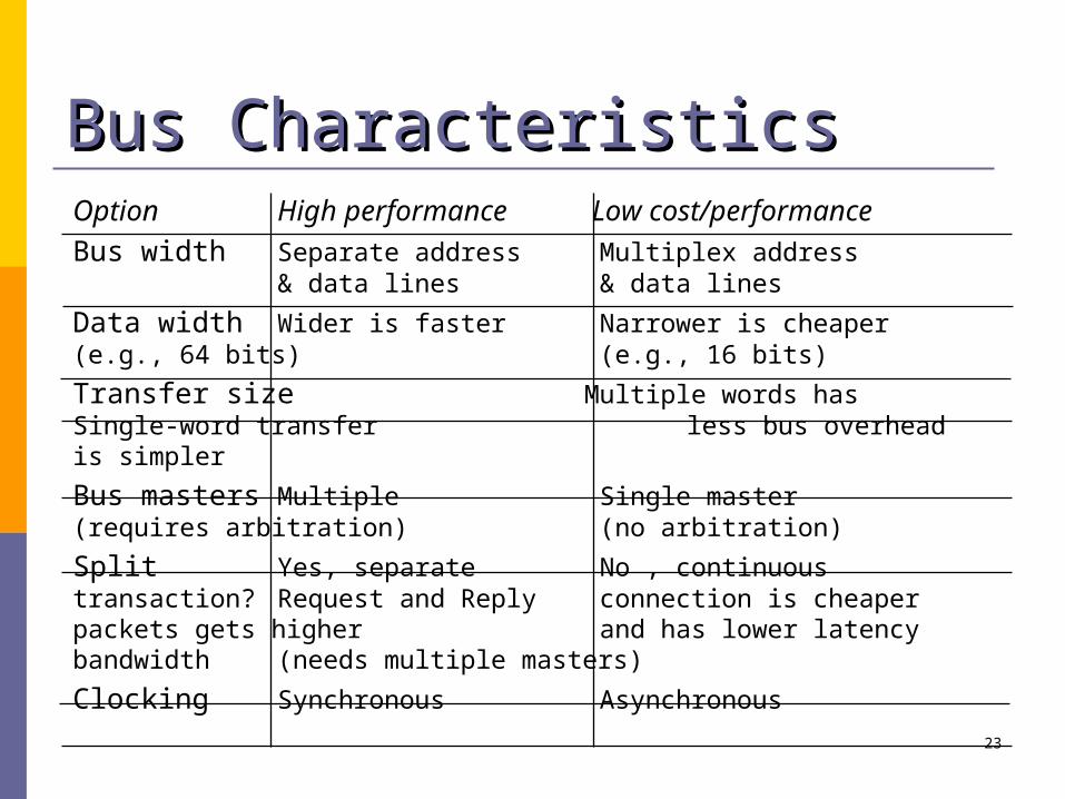
Bus CharacteristicsBus CharacteristicsOption High performance Low cost/performance
Bus width Separate address Multiplex address & data lines & data lines
Data width Wider is faster Narrower is cheaper (e.g., 64 bits) (e.g., 16 bits)
Transfer size Multiple words has Single-word transferless bus overhead is simpler
Bus masters Multiple Single master(requires arbitration) (no arbitration)
Split Yes, separate No , continuous transaction?Request and Reply connection is cheaper packets gets higher and has lower latencybandwidth(needs multiple masters)
Clocking Synchronous Asynchronous23

Storage IO Interfaces/BusesStorage IO Interfaces/Buses IDE/Ultra ATA SCSI
Data Width 16 bits 8 or 16 bits (wide)
Clock Rate Upto 100MHz 10MHz (Fast)
20MHz (Ultra)
40MHz (Ultra2)
80MHz (Ultra3)160MHz (Ultra4)
Bus Masters 1 Multiple
Max no. devices 2 7 (8-bit bus)
15 (16-bit bus)
Peak Bandwidth 200 MB/s 320MB/s (Ultra4)
2455:035 Computer Architecture and Organization

I/O Data Transfer Methods (1/2) Programmed I/O (PIO): Polling (For low-speed I/O)
The I/O device puts its status information in a status register. The processor must periodically check the status register. The processor is totally in control and does all the work. Very wasteful of processor time. Used for low-speed I/O devices (mice, keyboards etc.)
Time(workload) = Time(CPU) + Time(I/O) - Time(Overlap)
2555:035 Computer Architecture and Organization

I/O Data Transfer Methods (2/2) Interrupt-Driven I/O (For medium-speed I/O):
An interrupt line from the I/O device to the CPU is used to generate an I/O interrupt indicating that the I/O device needs CPU attention.
The interrupting device places its identity in an interrupt vector.
Once an I/O interrupt is detected the current instruction is completed and an I/O interrupt handling routine (by OS) is executed to service the device.
Used for moderate speed I/O (optical drives, storage, neworks ..)
Allows overlap of CPU processing time and I/O processing time
2655:035 Computer Architecture and Organization

I/O data transfer methods Direct Memory Access (DMA) (For high-speed I/O):
Implemented with a specialized controller that transfers data between an I/O device and memory independent of the processor.
The DMA controller becomes the bus master and directs reads and writes between itself and memory.
Interrupts are still used only on completion of the transfer or when an error occurs.
Low CPU overhead, used in high speed I/O (storage, network interfaces)
Allows more overlap of CPU processing time and I/O processing time than interrupt-driven I/O.
2755:035 Computer Architecture and Organization

DMA transfer step
DMA transfer steps: The CPU sets up DMA by supplying device identity, operation,
memory address of source and destination of data, the number of bytes to be transferred.
The DMA controller starts the operation. When the data is available it transfers the data, including generating memory addresses for data to be transferred.
Once the DMA transfer is complete, the controller interrupts the processor, which determines whether the entire operation is complete.
2855:035 Computer Architecture and Organization

Cache & I/O: The Stale Data ProblemCache & I/O: The Stale Data Problem Three copies of data, may exist in: cache, memory, disk.
Similar to cache coherency problem in multiprocessor systems. CPU or I/O (DMA) may modify/access one copy while other
copies contain stale (old) data.
Possible solutions:
Connect I/O directly to CPU cache: CPU performance suffers. With write-back cache, the operating system flushes caches into
memory (forced write-back) to make sure data is not stale in memory.
Use write-through cache; I/O receives updated data from memory (This uses too much memory bandwidth).
The operating system designates memory address ranges involved in I/O DMA operations as non-cacheable.
29

I/O Connected Directly To CacheI/O Connected Directly To Cache
This solutionmay slow down CPU performance
DMAI/O
A possible solution for A possible solution for the stale data problemthe stale data problem
However:However:CPU performance suffers
30

Factors Affecting PerformanceFactors Affecting Performance I/O processing computational requirements:
CPU computations available for I/O operations. Operating system I/O processing policies/routines. I/O Data Transfer/Processing Method: Polling, Interrupt Driven. DMA
I/O Subsystem performance: Raw performance of I/O devices (i.e magnetic disk performance). I/O bus capabilities. I/O subsystem organization. i.e number of devices, array level .. Loading level of I/O devices (queuing delay, response time).
Memory subsystem performance: Available memory bandwidth for I/O operations (For DMA)
Operating System Policies: File system vs. Raw I/O. File cache size and write Policy.
31
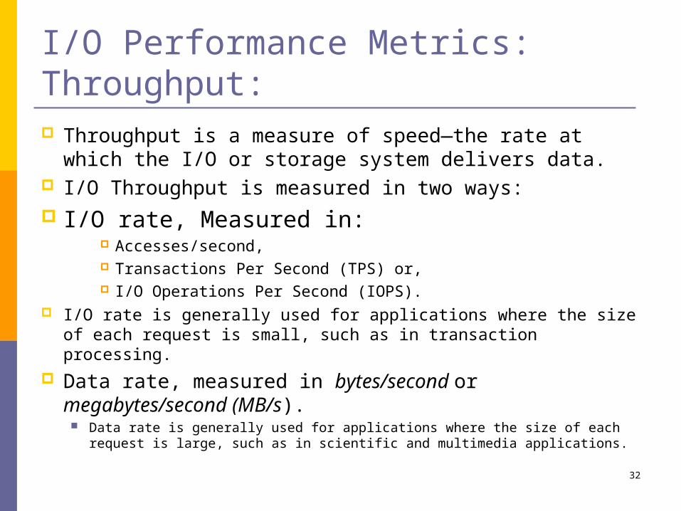
I/O Performance Metrics: Throughput: Throughput is a measure of speed—the rate at which the
I/O or storage system delivers data. I/O Throughput is measured in two ways: I/O rate, Measured in:
Accesses/second, Transactions Per Second (TPS) or, I/O Operations Per Second (IOPS).
I/O rate is generally used for applications where the size of each request is small, such as in transaction processing.
Data rate, measured in bytes/second or megabytes/second (MB/s).
Data rate is generally used for applications where the size of each request is large, such as in scientific and multimedia applications.
32

Seek Time
Magnetic DisksMagnetic DisksCharacteristics:Diameter (form factor): 2.5in - 5.25in Rotational speed: 3,600RPM-15,000 RPM Tracks per surface. Sectors per track: Outer tracks contain more sectors. Recording or Areal Density: Tracks/in X Bits/in Cost Per Megabyte. Seek Time: (2-12 ms) The time needed to move the read/write head arm. Reported values: Minimum, Maximum, Average. Rotation Latency or Delay: (2-8 ms) The time for the requested sector to be under the read/write head. (~ time for half a rotation) Transfer time: The time needed to transfer a sector of bits. Type of controller/interface: SCSI, EIDE Disk Controller delay or time. Average time to access a sector of data = average seek time + average rotational delay + transfer time + disk controller overhead (ignoring queuing time)
Current Rotation speed7200-15000 RPM
Access time = average seek time + average rotational delay
33

Read Access Steps
Memory mapped I/O over bus to controller Controller starts access Seek + rotational latency wait Sector is read and buffered (validity check) Controller DMA’s to memory and says ready
Access timeQueue + controller delay +block size/bandwidth
+ seek time + transfer time + check delay
3455:035 Computer Architecture and Organization
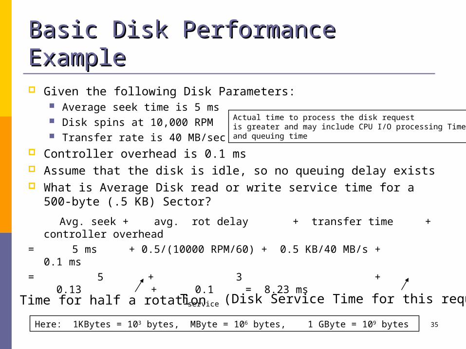
Basic Disk Performance ExampleBasic Disk Performance Example Given the following Disk Parameters:
Average seek time is 5 ms Disk spins at 10,000 RPM Transfer rate is 40 MB/sec
Controller overhead is 0.1 ms Assume that the disk is idle, so no queuing delay exists What is Average Disk read or write service time for a 500-byte (.5
KB) Sector?
Avg. seek + avg. rot delay + transfer time + controller overhead
= 5 ms + 0.5/(10000 RPM/60) + 0.5 KB/40 MB/s + 0.1 ms
= 5 + 3 + 0.13 + 0.1 = 8.23 msTime for half a rotation Tservice (Disk Service Time for this request)
Here: 1KBytes = 103 bytes, MByte = 106 bytes, 1 GByte = 109 bytes
Actual time to process the disk requestis greater and may include CPU I/O processing Timeand queuing time
35

Disk Arrays
14”10”5.25”3.5”
3.5”
Disk Array: 1 disk design
Conventional: 4 disk designs
Disk Product Families
Low End High End
3655:035 Computer Architecture and Organization

Array Reliability• Reliability of N disks = Reliability of 1 Disk / N
50,000 Hours / 70 disks = 700 hours
Disk system MTBF: Drops from 6 years to 1 month!
• Arrays (without redundancy) too unreliable to be useful!
Hot spares support reconstruction in parallel with access: very high media availability can be achieved
Hot spares support reconstruction in parallel with access: very high media availability can be achieved
3755:035 Computer Architecture and Organization

Redundant Array of Disks• Files are "striped" across multiple spindles• Redundancy yields high data availability
Disks will fail
Contents reconstructed from data redundantly stored in the array
Capacity penalty to store it
Bandwidth penalty to update
Mirroring/Shadowing (high capacity cost)
Horizontal Hamming Codes (overkill)
Parity & Reed-Solomon Codes
Failure Prediction (no capacity overhead!)VaxSimPlus — Technique is controversial
Techniques:
3855:035 Computer Architecture and Organization

RAID LevelsRaid level Failures Data disks Check
disks
0 Nonredundant 0 8 0
1 Mirrored 1 8 8
2 Memory-style ECC 1 8 4
3 Bit-interleaved parity 1 8 1
4 Block-interleaved parity 1 8 1
5 Block-interleaved distributed parity 1 8 1
6 P+Q redundancy add 2nd parity 2 8 2
39

Raid 1: Disk Mirroring
• Each disk is fully duplicated onto its "shadow" Very high availability can be achieved
• Bandwidth sacrifice on write: Logical write = two physical writes
• Reads may be optimized
• Most expensive solution: 100% capacity overhead
Targeted for high I/O rate, high availability environments
recoverygroup
4055:035 Computer Architecture and Organization

Raid 3: Parity Disk100100111100110110010011
. . .
logical record
10010011
11001101
10010011
00110000
P
Striped physicalrecords
• Parity computed across recovery group to protect against HD failures• 33% capacity cost for parity in this configuration• wider arrays reduce capacity costs, decrease expected availability, increase reconstruction time
• Arms logically synchronized, spindles rotationally synchronized logically a single high capacity, high transfer rate disk
Targeted for high bandwidth applications: Scientific, Image Processing 41
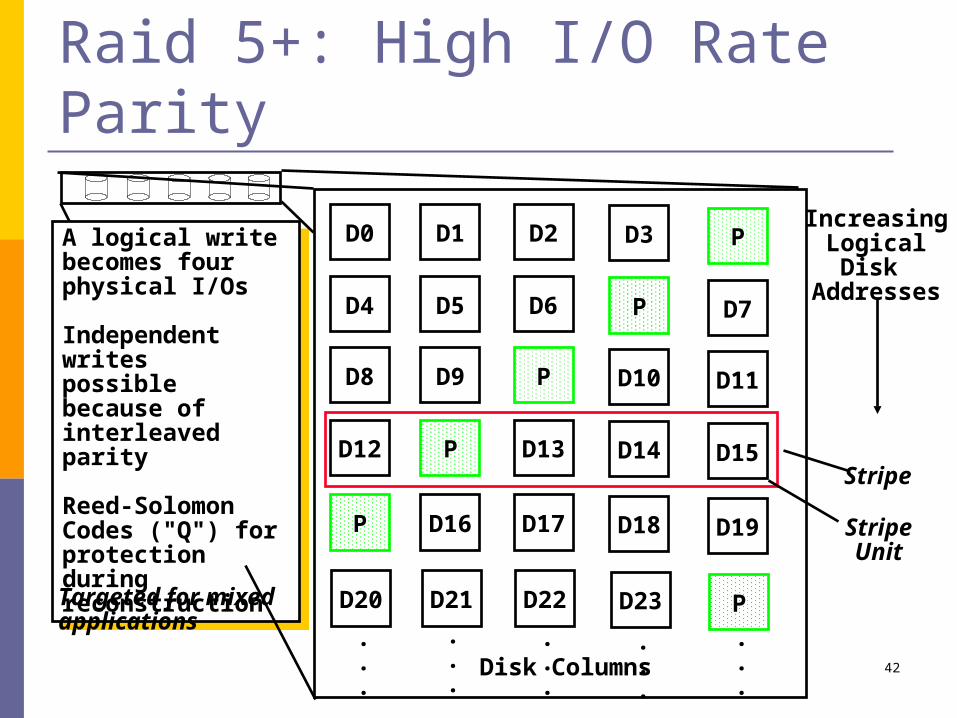
Raid 5+: High I/O Rate Parity
A logical writebecomes fourphysical I/Os
Independent writespossible because ofinterleaved parity
Reed-SolomonCodes ("Q") forprotection duringreconstruction
A logical writebecomes fourphysical I/Os
Independent writespossible because ofinterleaved parity
Reed-SolomonCodes ("Q") forprotection duringreconstruction
D0 D1 D2 D3 P
D4 D5 D6 P D7
D8 D9 P D10 D11
D12 P D13 D14 D15
P D16 D17 D18 D19
D20 D21 D22 D23 P
.
.
.
.
.
.
.
.
.
.
.
.
.
.
.Disk Columns
IncreasingLogical
Disk Addresses
Stripe
StripeUnit
Targeted for mixedapplications
42

Subsystem Organization
hostarray
controller
single boarddisk
controller
single boarddisk
controller
single boarddisk
controller
single boarddisk
controller
hostadapter
manages interfaceto host, DMA
control, buffering,parity logic
physical devicecontrol
often piggy-backedin small format devices
striping software off-loaded from host to array controller
no applications modifications
no reduction of host performance 43

System Availability
ArrayController
StringController
StringController
StringController
StringController
StringController
. . .
. . .
. . .
. . .
. . .
Data Recovery Group: unit of data redundancy
Redundant Support Components: fans, power supplies, controller, cables
End to End Data Integrity: internal parity protected data paths44

System-Level Availability
RecoveryGroup
Goal: No SinglePoints ofFailure
Goal: No SinglePoints ofFailure
Fully dual redundantI/O Controller I/O Controller
Array Controller Array Controller
. . .
. . .
. . .
. . . . . .
.
.
.
host host
with duplicated paths, higher performance can beobtained when there are no failures 45

Peripheral Component Interconnect 2 Types of Agents on the Bus
Initiator (master) Target
3 Address Spaces Memory IO Configuration
Transactions done in 2 (or more) phases Address/Command Data/Byte Enable Phase(s)
Synchronous Operation (positive edge of clock)
55:035 Computer Architecture and Organization 46

Typical PCI Topology
55:035 Computer Architecture and Organization 47
memory
Host
PCI bridge
EthernetPrinterDisk
interf ace
PCI bus
Main

PCI Signals
55:035 Computer Architecture and Organization 48
Name Function
CLK A 33-MHzor 66-MHzclock.
FRAME# Sent by the initiator to indicate the start and duration of a transaction.
AD 32 address/datalines,which may beoptionallyincreasedto 64.
C/BE# 4 command/byte enable lines (8 for a 64-bit bus.)
IRDY#, TRD Y# Initiator-readyand Target-readysignals.
DEVSEL# Aresponsefromthedeviceindicatingthat it hasrecognizeditsaddressand isready for a datatransfertransaction.
IDSEL# InitializationDeviceSelect.

PCI Read
55:035 Computer Architecture and Organization 49
1 2 3 4 5 6 7
CLK
Frame#
AD
C/BE#
IRDY#
TRDY#
DEVSEL#
Adress #1 #4
Cmnd Byte enable
#2 #3