Embed Size (px)
Citation preview
International Journal of Advances in Engineering & Technology, June, 2016.
©IJAET ISSN: 22311963
310 Vol. 9, Issue 3, pp. 310-320
AN OPTIMIZED LOW-VOLTAGE LOW-POWER DOUBLE TAIL
COMPARATOR FOR HIGH-SPEED ADCS
1P. Rajesh, 2M. Priyanka, 3P. Nalini, 4M. Chandra Mouli 1Assistant Professor, 2,3,4B.Tech Student
ECE Department, Raghu Engineering College, Visakhapatnam, India
ABSTRACT As today’s world has become smart i.e,digitalization has been spreading rapidly, the need for ultra low-power
,area efficient and highspeed analog -to-digital converters is pushing towards the use of dynamic regenerative
comparator to maximise the speed and power efficiency. In this paper, a dynamic double tail comparator with
positive feed-back for latch regeneration has been designed with high-speed and low-offset. Simulations are
carried out in 180nm and 90 nm CMOS technology. In the resultant comparator power dissipation and delay
are reduced.
KEYWORDS: Digitalization, Dynamic, Double Tail, Latch Regeneration, Offset
I. INTRODUCTION
In modern life, electronic equipment is frequently used in all fields such as communication,
transportation, entertainment, medical, household etc. The requirement of analog to digital converters
is increasing day by day as they play a major role in converting the analog signals to digital
ones.ADCs act as interface between the natural analog world and the real time digital world.
Comparator is the fundamental block which acts as heart of the ADC. In general ,a comparator is
defined as an electronic device which compares the given analog input signal with reference voltage
and produces a digital output i.e, either logic ‘0’ or logic ‘1’. If the input to the non-inverting input is
greater than that to the inverting input, the output is a logical 1. If the input to the non-inverting input
is less than that to the inverting input, the output is a logical 0.
In this paper, Open loop comparators, pre-amplifier based comparators and dynamic comparators are
discussed and a dynamic comparator is proposed to overcome the disadvantages of the previous
topologies. The open loop comparator does not possess a clock input, due to which the output is
generated randomly without a particular timing. On the other hand pre-amplifier based comparators
make use of clock and achieve less offset voltage but suffer from static power dissipation and stacking
[1]. This proposed dynamic comparator operated with low- voltage because of less stacking and
achieves low-offset, high speed, low-power dissipation and high operating performance [1],[5].
This paper is organized as follows. Section II provides an overview of the various comparator
topologies in terms of their advantages and drawbacks, and section III describes the analysis of
proposed dynamic latched comparator. Section IV provides schematics of conventional and proposed
dynamic latched comparators which are drawn in S-Edit. Simulation results obtained from HSPICE
using 180nm and 90nm PTM technology [7] and their comparisons are presented in Section V and
conclusion is drawn in Section VI.
II. COMPARATOR ARCHITECTURE AND TOPOLOGIES
Architectures of voltage comparators will be classified into three types: Open-loop Comparators (op-
amps without compensation), Pre-amplifier Based Latched Comparators (open-loop comparator
International Journal of Advances in Engineering & Technology, June, 2016.
©IJAET ISSN: 22311963
311 Vol. 9, Issue 3, pp. 310-320
combined with dynamic regenerative latch), and Fully Dynamic Latched Comparator. The following
Figure 1 illustrates the various blocks involved in the dynamic latched comparator.
Fig. 1: High Speed Comparator Architecture
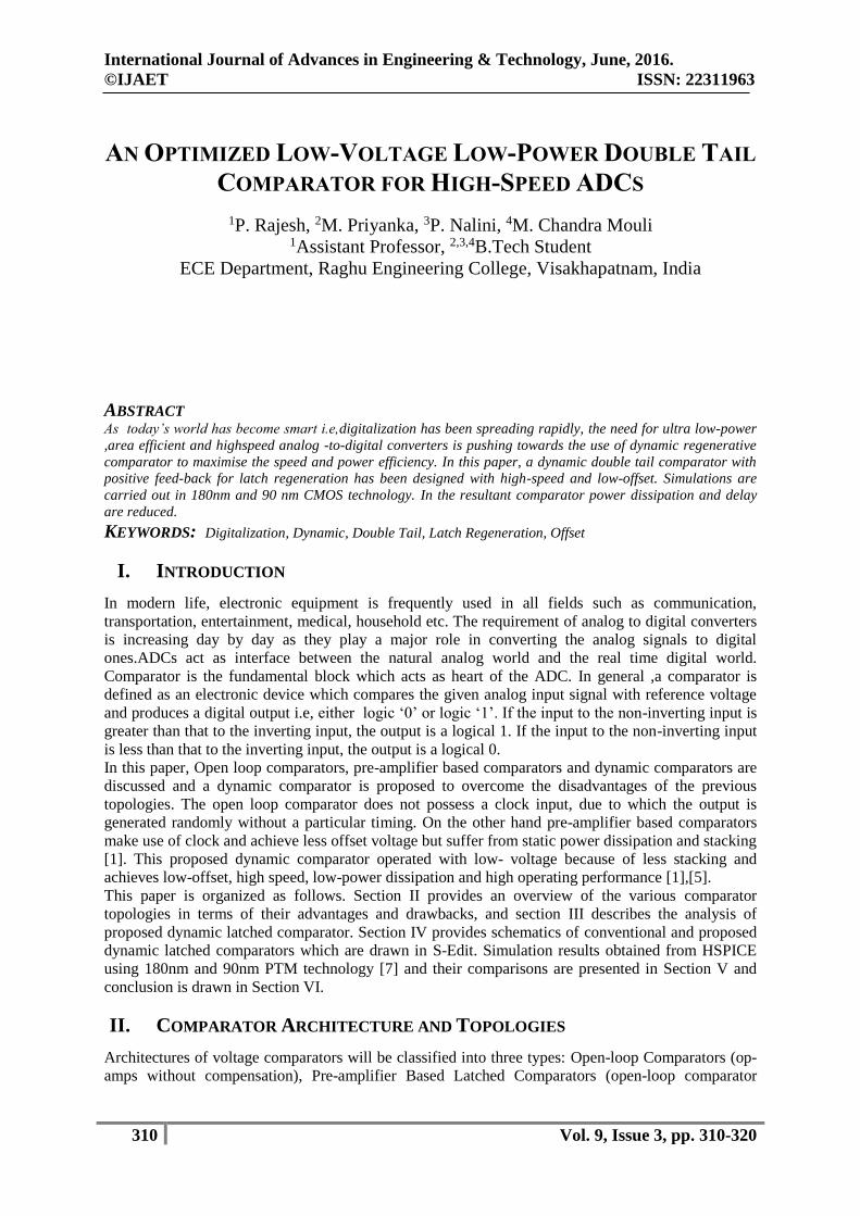
Open-loop, continuous time comparator, shown in Figure 2, is an operational amplifier without
frequency compensation to obtain the largest possible bandwidth, hence improving its time response.
Since the precise gain and linearity are of no interest in comparator design, no-compensation does not
pose a problem. However, due to its limited gain-bandwidth product, open-loop comparators are too
slow for many applications.
Fig. 2: Open-Loop Comparator
One the other hand, a cascade of open-loop amplifiers usually has a significantly larger gain-
bandwidth product than a single-stage amplifier with the same gain. However, since it costs more area
and power consumption [1], cascading does not give practical advantages for many applications.
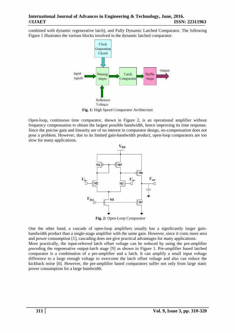
More practically, the input-referred latch offset voltage can be reduced by using the pre-amplifier
preceding the regenerative output-latch stage [9] as shown in Figure 1. Pre-amplifier based latched
comparator is a combination of a pre-amplifier and a latch. It can amplify a small input voltage
difference to a large enough voltage to overcome the latch offset voltage and also can reduce the
kickback noise [6]. However, the pre-amplifier based comparators suffer not only from large static
power consumption for a large bandwidth.
International Journal of Advances in Engineering & Technology, June, 2016.
©IJAET ISSN: 22311963
312 Vol. 9, Issue 3, pp. 310-320
Fig. 3: Pre-Amplifier Based Latched Comparator
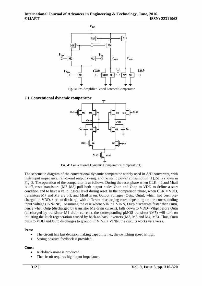
2.1 Conventional dynamic comparator
Fig. 4: Conventional Dynamic Comparator (Comparator 1)
The schematic diagram of the conventional dynamic comparator widely used in A/D converters, with
high input impedance, rail-to-rail output swing, and no static power consumption [1],[5] is shown in
Fig. 3. The operation of the comparator is as follows. During the reset phase when CLK = 0 and Mtail
is off, reset transistors (M7–M8) pull both output nodes Outn and Outp to VDD to define a start
condition and to have a valid logical level during reset. In the comparison phase, when CLK = VDD,
transistors M7 and M8 are off, and Mtail is on. Output voltages (Outp, Outn), which had been pre-
charged to VDD, start to discharge with different discharging rates depending on the corresponding
input voltage (INN/INP). Assuming the case where VINP > VINN, Outp discharges faster than Outn,
hence when Outp (discharged by transistor M2 drain current), falls down to VDD–|Vthp| before Outn
(discharged by transistor M1 drain current), the corresponding pMOS transistor (M5) will turn on
initiating the latch regeneration caused by back-to-back inverters (M3, M5 and M4, M6). Thus, Outn
pulls to VDD and Outp discharges to ground. If VINP < VINN, the circuits works vice versa.
Pros:
The circuit has fast decision making capability i.e., the switching speed is high.
Strong positive feedback is provided.
Cons:
Kick-back noise is produced.
The circuit requires high input impedance.
International Journal of Advances in Engineering & Technology, June, 2016.
©IJAET ISSN: 22311963
313 Vol. 9, Issue 3, pp. 310-320
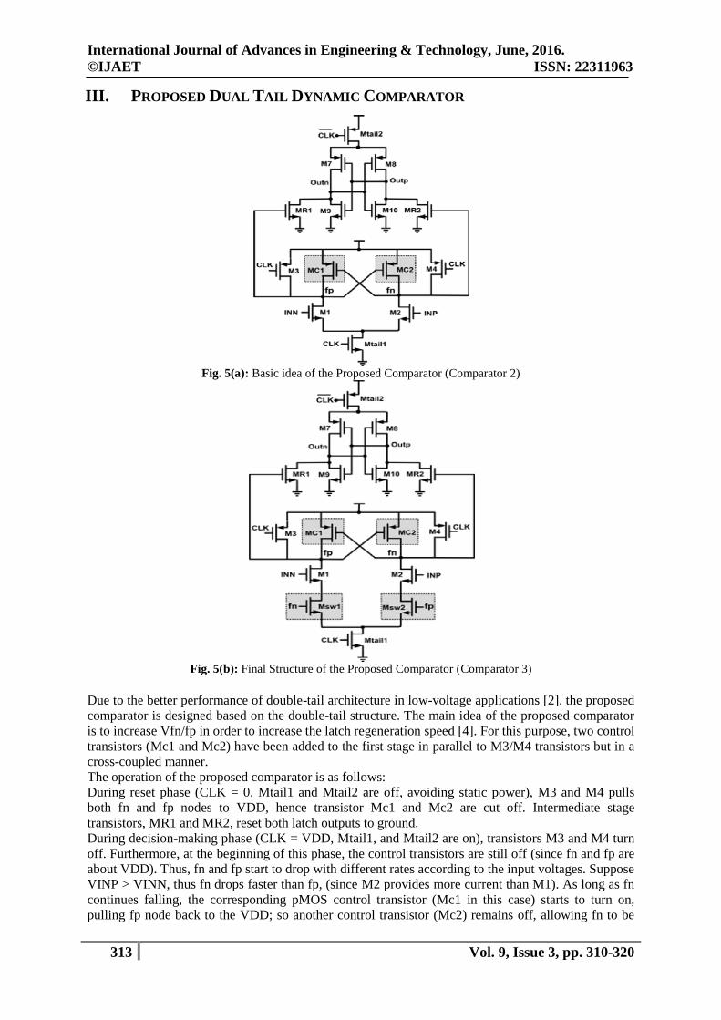
III. PROPOSED DUAL TAIL DYNAMIC COMPARATOR
Fig. 5(a): Basic idea of the Proposed Comparator (Comparator 2)
Fig. 5(b): Final Structure of the Proposed Comparator (Comparator 3)
Due to the better performance of double-tail architecture in low-voltage applications [2], the proposed
comparator is designed based on the double-tail structure. The main idea of the proposed comparator
is to increase Vfn/fp in order to increase the latch regeneration speed [4]. For this purpose, two control
transistors (Mc1 and Mc2) have been added to the first stage in parallel to M3/M4 transistors but in a
cross-coupled manner.
The operation of the proposed comparator is as follows:
During reset phase (CLK = 0, Mtail1 and Mtail2 are off, avoiding static power), M3 and M4 pulls
both fn and fp nodes to VDD, hence transistor Mc1 and Mc2 are cut off. Intermediate stage
transistors, MR1 and MR2, reset both latch outputs to ground.
During decision-making phase (CLK = VDD, Mtail1, and Mtail2 are on), transistors M3 and M4 turn
off. Furthermore, at the beginning of this phase, the control transistors are still off (since fn and fp are
about VDD). Thus, fn and fp start to drop with different rates according to the input voltages. Suppose
VINP > VINN, thus fn drops faster than fp, (since M2 provides more current than M1). As long as fn
continues falling, the corresponding pMOS control transistor (Mc1 in this case) starts to turn on,
pulling fp node back to the VDD; so another control transistor (Mc2) remains off, allowing fn to be

International Journal of Advances in Engineering & Technology, June, 2016.
©IJAET ISSN: 22311963
314 Vol. 9, Issue 3, pp. 310-320
dischargedcompletely. In other words, unlike conventional double-tail dynamic comparator, in which
Vfn/fp is just a function of input transistor transconductance and input voltage difference in the
proposed structure as soon as the comparator detects that for instance node fn discharges faster, a
pMOS transistor (Mc1) turns on, pulling the other node fp back to the VDD.Therefore by the time
passing, the difference between fn and fp (Vfn/fp) increases in an exponential manner, leading to the
reduction of latch regeneration time . Despite the effectiveness of the proposed idea, one of the points
which should be considered is that in this circuit, when one of the control transistors (e.g., Mc1) turns
on, a current from VDD is drawn to the ground via input and tail transistor (e.g., Mc1, M1, and
Mtail1), resulting in static power consumption. To overcome this issue, two nMOS switches are used
below the input transistors [Msw1 and Msw2].
At the beginning of the decision making phase, due to the fact that both fn and fp nodes have been
pre-charged to VDD (during the reset phase), both switches are closed and fn and fp start to drop with
different discharging rates. As soon as the comparator detects that one of the fn/fp nodes is
discharging faster, control transistors will act in a way to increase their voltage difference. Suppose
that fp is pulling up to the VDD and fn should be discharged completely, hence the switch in the
charging path of fp will be opened (in order to prevent any current drawn from VDD) but the other
switch connected to fn will be closed to allow the complete discharge of fn node. In other words, the
operation of the control transistors with the switches emulates the operation of the latch.
Pros and Cons:
In, the main idea of the proposed comparator control transistors are used which results in the
increase of latch regeneration speed. But there is an increase in the number of transistors as
well as the power dissipation of the circuit is high.
In the final structure, even though the numbers of transistors are more, power dissipation &
delay of the circuit is reduced and the circuit operates with high speed.
IV. SCHEMATICS AND SIMULATED WAVEFORMS
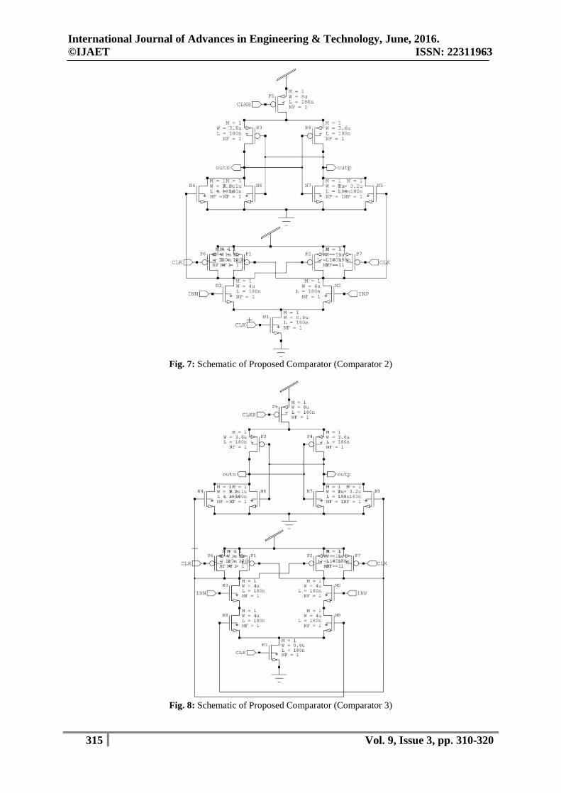
3.1 Schematics:
All the comparators schematics are drawn in S-Edit of Tanner Tools and from which netlists are
extracted, which are given as input files for the H-Spice. Simulations are carried out in H-Spice and
waveforms are generated using Avanwaves.
Fig. 6: Schematic of Conventional Dynamic Comparator (Comparator1)
International Journal of Advances in Engineering & Technology, June, 2016.
©IJAET ISSN: 22311963
315 Vol. 9, Issue 3, pp. 310-320
Fig. 7: Schematic of Proposed Comparator (Comparator 2)
Fig. 8: Schematic of Proposed Comparator (Comparator 3)
International Journal of Advances in Engineering & Technology, June, 2016.
©IJAET ISSN: 22311963
316 Vol. 9, Issue 3, pp. 310-320
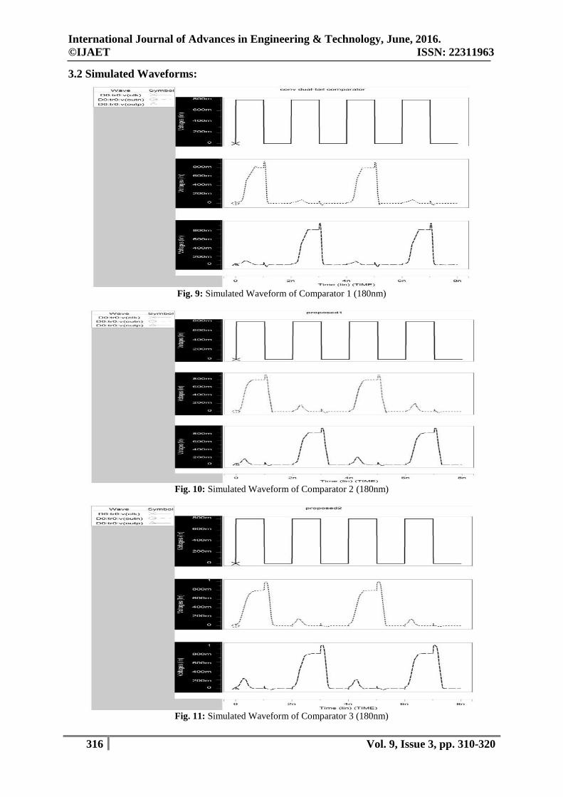
3.2 Simulated Waveforms:
Fig. 9: Simulated Waveform of Comparator 1 (180nm)
Fig. 10: Simulated Waveform of Comparator 2 (180nm)
Fig. 11: Simulated Waveform of Comparator 3 (180nm)
International Journal of Advances in Engineering & Technology, June, 2016.
©IJAET ISSN: 22311963
317 Vol. 9, Issue 3, pp. 310-320
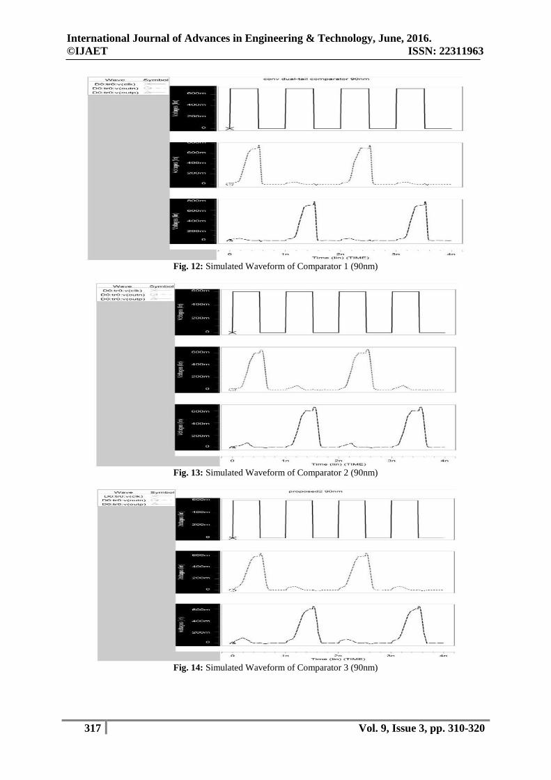
Fig. 12: Simulated Waveform of Comparator 1 (90nm)
Fig. 13: Simulated Waveform of Comparator 2 (90nm)
Fig. 14: Simulated Waveform of Comparator 3 (90nm)
International Journal of Advances in Engineering & Technology, June, 2016.
©IJAET ISSN: 22311963
318 Vol. 9, Issue 3, pp. 310-320
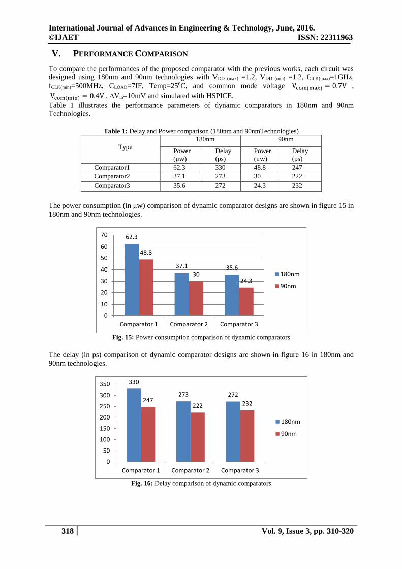
V. PERFORMANCE COMPARISON
To compare the performances of the proposed comparator with the previous works, each circuit was
designed using 180nm and 90nm technologies with VDD (max) =1.2, VDD (min) =1.2, fCLK(max)=1GHz,
fCLK(min)=500MHz, CLOAD=7fF, Temp=250C, and common mode voltage Vcom(max) = 0.7V ,
Vcom(min) = 0.4V , ∆Vin=10mV and simulated with HSPICE.
Table 1 illustrates the performance parameters of dynamic comparators in 180nm and 90nm
Technologies.
Table 1: Delay and Power comparison (180nm and 90nmTechnologies)
Type
180nm 90nm
Power
(μw)
Delay
(ps)
Power
(μw)
Delay
(ps)
Comparator1 62.3 330 48.8 247
Comparator2 37.1 273 30 222
Comparator3 35.6 272 24.3 232
The power consumption (in μw) comparison of dynamic comparator designs are shown in figure 15 in
180nm and 90nm technologies.
Fig. 15: Power consumption comparison of dynamic comparators
The delay (in ps) comparison of dynamic comparator designs are shown in figure 16 in 180nm and
90nm technologies.
Fig. 16: Delay comparison of dynamic comparators
62.3
37.1 35.6
48.8
3024.3
0
10
20
30
40
50
60
70
Comparator 1 Comparator 2 Comparator 3
180nm
90nm
330
273 272247
222 232
0
50
100
150
200
250
300
350
Comparator 1 Comparator 2 Comparator 3
180nm
90nm

International Journal of Advances in Engineering & Technology, June, 2016.
©IJAET ISSN: 22311963
319 Vol. 9, Issue 3, pp. 310-320
VI. CONCLUSION
In this paper, the comparator circuits for high-speed ADCs have been presented. The conventional
dynamic and conventional double tail comparators have been simulated with 180nm and 90nm CMOS
technology using H-Spice and their performance parameters such as power and delay are compared.
The proposed dynamic comparator (Comparator 3) shows minimal power consumption of 35.6 µW
and 24.3 µW, minimal propagation time delay of 272 ps and 232 ps in 180nm and 90nm respectively.
The proposed comparator is best suitable for low power high-speed ADCs.
REFERENCES:
[1]. B. Wicht, T. Nirschl, and D. Schmitt-Landsiedel, “Yield and speed optimization of a latch-type voltage
sense amplifier,” IEEE J. Solid-State Circuits, vol. 39, pp. 1148-1158, July 2004.
[2]. D. Schinkel, E. Mensink, E. Kiumperink, E. van Tuijl and B. Nauta, “A Double-Tail Latch-Type
Voltage Sense Amplifier with 18ps Setup+Hold Time,” ISSCC Dig. Tech. Papers, pp. 314-315 and
605, Feb. 2007.
[3]. M. Miyahara, Y. Asada, P. Daehwa and A. Matsuzawa, “A Low-Noise Self-Calibrating Dynamic
Comparator for High-Speed ADCs,” in Proc. A-SSCC, pp. 269-272, Nov. 2008.
[4]. A. Nikoozadeh and B. Murmann, “An Analysis of Latch Comparator Offset Due to Load Capacitor
Mismatch,” IEEE Trans. Circuits Syst. II: Exp. Briefs, vol. 53, no. 12, pp. 1398-1402, Dec. 2006 Philip
E. Allen and Douglas R. Holberg, CMOS Analog Circuit Design, 2nd ed. New York, NY: Oxford,
2002.
[5]. S. Kale and R. S. Gamad, “Design of a CMOS Comparator for Low Power and High Speed,”
Internationl Journal of Electronic Engineering Research, vol. 2, no. 1, pp. 29-34, 2010
[6]. Pedro M.Figueiredo, Joao C.Vital, “Kickback Noise Reduction Techniques for CMOS Latched
Comparator”, IEEE Transactions on Circuits and Systems, vol.53, no.7, pp.541- 545, July 2006.
[7]. 90nm Predictive Technology Model (PTM), [Online]Available:http://www.eas.asu.edu/~ptm/latest.htm
[8]. Sumanen, M. Waltari, V. Hakkarainen, K. Halonen, “CMOS Dynamic Comparators for Pipeline A/D
Converters,” IEEE ISCAS, vol. 5, pp. 157 - 160, May 2002.
[9]. Jeon, Heung Jun, "Low-power high-speed low-offset fully dynamic CMOS latched comparator"
(2010).
[10]. Philip E. Allen and Douglas R. Holberg, CMOS Analog Circuit Design, 2nd Ed. New York, NY:
Oxford, 2002.
[11]. D. N. Kapadia and P. P. Gandhi, “Implementation of CMOS charge sharing dynamic latch comparator
in 130 nm and 90 nm technologies,” in Proceedings of the IEEE Conference on Information and
Communication Technologies (ICT '13), pp. 16–20, JeJu Island, Republic of Korea, April 2013.
[12]. Samaneh Babayan-Mashhadi, Student Member, IEEE, and Reza Lotfi, Member, IEEE, “Analysis and
Design of a Low-Voltage Low-Power Double-Tail Comparator”, IEEE Transactions on Very Large
Scale Integration (VLSI) Systems, Vol. 22, No. 2, February 2014.
AUTHORS
P. Rajesh received his B.Tech degree from Raghu Engineering College in the year 2011 and
received M.Tech degree from MVGR College of Engineering in the year 2013. He is working as
an Assistant Professor in the Department of Electronics and Communication Engineering at
Raghu Engineering College. He has published four Papers in International Journals. His research
activities are related to Low power VLSI Design.
M. Priyanka presently pursuing his B.Tech in Electronics and Communication Engineering,
Raghu Engineering College.

International Journal of Advances in Engineering & Technology, June, 2016.
©IJAET ISSN: 22311963
320 Vol. 9, Issue 3, pp. 310-320
P. Nalini presently pursuing his B.Tech in Electronics and Communication Engineering, Raghu
Engineering College.
M. Chandra Mouli presently pursuing his B.Tech in Electronics and Communication
Engineering, Raghu Engineering College.