Embed Size (px)
Citation preview
ASAP High-Density Metal Programmable Library for TSMC 0.18um G FSG Standard Vt Process
User’s Manual
(c) 1999-2005 Virage Logic Corporation, All Rights Reserved (copyright notice reflects distribution which may not necessarily be a publication).
Virage Logic Corporation47100 Bayside ParkwayFremont, California 94538 USA
This product and document are protected by copyright and distributed under licenses restricting their use, copying, distribution and decompilation. The material in this manual may not be reproduced, adapted, merged, translated, stored or used without prior written approval of Virage Logic.
RESTRICTED RIGHTS LEGEND: Use, duplication, or disclosure by the government is subject to restrictions as set forth in subparagraph (c)(1)(ii) of the Rights in Technical Data and Computer Software clause at DFARS 252.227-7013 and FAR 52.227-19.
The product described in this manual may be protected by one or more U.S. patents, foreign patents, or pending patent applications.
TRADEMARKS
The license manager portion of this product is based on FLEXlm license Manager from Macrovision Corporation. All Virage Logic products (STMC) are trademarks of Virage Logic Corporation. Embed-It!® is a registered trademark of Virage Logic Corporation. All other product and company names used in this document may be trademarks of their respective owners.
The information furnished in this manual is believed to be accurate at the time of printing. Virage Logic Corporation reserves the right to make changes to any products or services herein at any time without notice. Virage Logic does not assume any responsibility or liability arising out of the application or use of any product or service described herein, except as expressly agreed to in writing by Virage Logic; nor does the purchase, lease, or use of a product or service from Virage Logic Corporation convey a license under any patent rights, copyright, trademark right, or any other intellectual property rights of Virage Logic or third parties.
THIS PUBLICATION IS PROVIDED “AS IS” WITHOUT WARRANTY OF ANY KIND, EITHER EXPRESS OR IMPLIED, INCLUDING, BUT NOT LIMITED TO, THE IMPLIED WARRANTIES OF MERCHANTABILITY, FITNESS FOR A PARTICULAR PURPOSE, OR NON-INFRINGEMENT.
ts18ugfsdmp
LPED-0038
ii Virage Logic Corporation
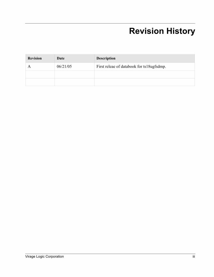
Revision History
Revision Date Description
A 06/21/05 First releae of databook for ts18ugfsdmp.
Virage Logic Corporation iii

iv Virage Logic Corporation
Contents
Revision History................................................................................................................. iii
Contents ........................................................................................................................ v
Chapter 1 Introduction ...................................................................................................... 11.1 ASAP Logic ..................................................................................................................... 11.2 Logic Libraries................................................................................................................. 11.3 This Manual ..................................................................................................................... 21.4 Technical Assistance........................................................................................................ 2
Chapter 2 Introduction to NXT Architecture ................................................................... 32.1 NXT Architecture ............................................................................................................ 32.2 Optimizing Floorplanning and Placement ....................................................................... 32.3 Optimizing Power Routing .............................................................................................. 42.4 Optimizing Routing ......................................................................................................... 4
Chapter 3 Design Guidelines............................................................................................ 53.1 Technology Setup ............................................................................................................ 5
3.1.1 Setup for Cadence Design Systems Tools ......................................................... 53.1.2 Setup for Synopsys' Apollo/Astro Physical Design Tools................................. 6
3.2 High-Level Architecture .................................................................................................. 63.2.1 Power and Electromigration............................................................................... 63.2.2 CMOS Power Consumption............................................................................... 63.2.3 Operating Frequency.......................................................................................... 73.2.4 Switching Factor ................................................................................................ 7
3.3 Routing Directions and Power Grid Routing................................................................... 73.3.1 Routing Power Straps on Grid ........................................................................... 73.3.2 Routing Power Straps to Balance Signal Routing Resources ............................ 93.3.3 Using a Conventional Power Routing Scheme .................................................. 9
3.4 Special Cells .................................................................................................................. 103.4.1 Clock Driver Cell Usage .................................................................................. 103.4.2 Tri-State Cell Usage......................................................................................... 113.4.3 Delay Cell Usage.............................................................................................. 123.4.4 Filler Cell Usage .............................................................................................. 123.4.5 Variable Width Power and Ground Cell Rails................................................. 13
Chapter 4 Library Characteristics.................................................................................. 154.1 Physical Characteristics ................................................................................................. 15
4.1.1 Example ........................................................................................................... 16
Virage Logic Corporation v
Contents
4.2 Electrical Characteristics ............................................................................................... 164.3 Electromigration Limit .................................................................................................. 174.4 Loading and Slew Rate.................................................................................................. 17
Chapter 5 Datasheets ...................................................................................................... 215.1 Cell Selection Philosophy.............................................................................................. 21
5.1.1 Synthesis Friendly............................................................................................ 215.1.2 Place and Route Friendly ................................................................................. 215.1.3 Optimized Performance and Power ................................................................. 22
5.2 Cell Function Summary................................................................................................. 225.3 Naming Conventions ..................................................................................................... 23
5.3.1 Cell Naming Syntax......................................................................................... 235.3.2 Examples.......................................................................................................... 23
5.4 Datasheets ...................................................................................................................... 245.4.1 Combinational Cells ........................................................................................ 255.4.2 Sequential Cells ............................................................................................... 295.4.3 Special Cells..................................................................................................... 32
Chapter 6 Characterization Methodology...................................................................... 356.1 Input Pin Capacitance .................................................................................................... 356.2 Combinational Pin-to-Pin Delays .................................................................................. 356.3 Output Pin Transition Times ......................................................................................... 356.4 Dynamic Power Dissipation .......................................................................................... 366.5 Timing Check Constraints ............................................................................................. 366.6 Steady-State Power Dissipation..................................................................................... 36
Chapter 7 Modeling Methodology and Validation ....................................................... 377.1 Standard List of Models ................................................................................................ 377.2 Quality Assurance Methodology ................................................................................... 377.3 Explanation of Physical Models .................................................................................... 38
7.3.1 Full Layout Database ....................................................................................... 387.3.2 Cell Place-and-Route Abstract Model ............................................................. 39
vi Virage Logic Corporation
Chapter 1 Introduction
1.1 ASAP Logic
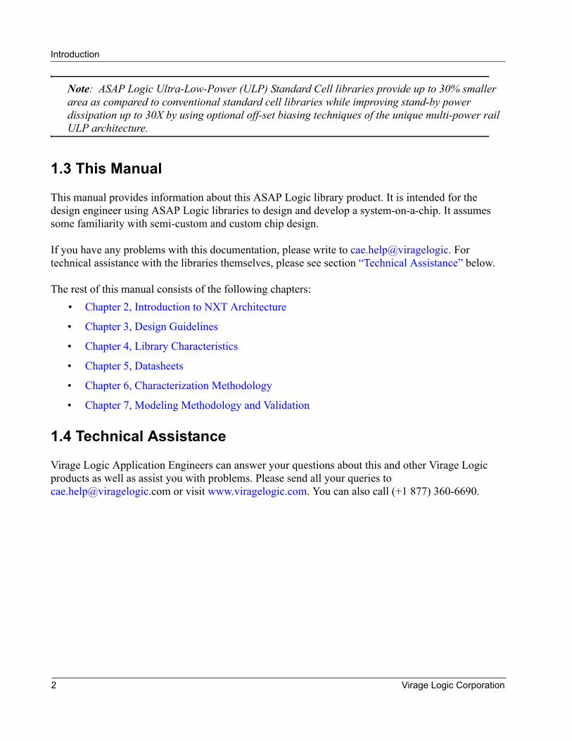
The ASAP Logic libraries are based on Virage Logic's proprietary and patented NXT routing and cell architecture. This architecture has been proven across a wide range of designs, including high volume production, with over 2500 products.
The NXT architecture’s innovative approach to routing and cell design consistently yields smaller designs without sacrificing performance. Virage Logic's NXT architecture offers up to a 20% improvement in utilization. Depending on your design needs, this increase in utilization budget can be allocated to attain various goals:
• Higher density without a loss of performance
• Lower power
• Higher performance without an increase in area
• Mask cost reduction
1.2 Logic Libraries
The ASAP Logic family is comprised of Metal-Programmable and Standard Cell libraries optimized for different tasks. Within each product family are several architectures that are application-optimized libraries targeted to a variety of market requirements: High-Speed, High-Density, Ultra-High-Density and Ultra-Low-Power.
Each ASAP Logic architecture is developed to fit a particular target process and application segment. All cells come with hand optimized circuit design and layout for optimized performance, power consumption, and minimized raw cell area. ASAP Logic cell libraries are correlated to silicon for maximum accuracy and predictability of results.
The ASAP Logic Standard Cell libraries may be available with or without taps depending on the specific architecture.
In addition, the cells in these libraries are: • Optimized for Synthesis through the careful selection of the cell set
• Optimized for Place and Route by improving pin access
• Optimized for Performance and Power by providing a choice of drive strengths
Virage Logic Corporation 1
Introduction
Note: ASAP Logic Ultra-Low-Power (ULP) Standard Cell libraries provide up to 30% smaller area as compared to conventional standard cell libraries while improving stand-by power dissipation up to 30X by using optional off-set biasing techniques of the unique multi-power rail ULP architecture.
1.3 This Manual
This manual provides information about this ASAP Logic library product. It is intended for the design engineer using ASAP Logic libraries to design and develop a system-on-a-chip. It assumes some familiarity with semi-custom and custom chip design.
If you have any problems with this documentation, please write to cae.help@viragelogic. For technical assistance with the libraries themselves, please see section “Technical Assistance” below.
The rest of this manual consists of the following chapters:• Chapter 2, Introduction to NXT Architecture
• Chapter 3, Design Guidelines
• Chapter 4, Library Characteristics
• Chapter 5, Datasheets
• Chapter 6, Characterization Methodology
• Chapter 7, Modeling Methodology and Validation
1.4 Technical Assistance
Virage Logic Application Engineers can answer your questions about this and other Virage Logic products as well as assist you with problems. Please send all your queries [email protected] or visit www.viragelogic.com. You can also call (+1 877) 360-6690.
2 Virage Logic Corporation
Chapter 2 Introduction to NXT Architecture
2.1 NXT Architecture
In designs using NXT architecture, the preferred direction for routing metal2 is parallel to the cell power/ground (P/G) rails; this routing direction is conventionally referred to as “horizontal”. The preferred routing directions in the cell layouts naturally extend to routing at the block and chip level as well. As a result, the preferred routing directions in NXT routing are vertical for the first layer, horizontal for the second layer, vertical for the third layer, and so on. To use the conventional notation, this is a VHVH routing scheme. This preferred routing scheme for NXT routing is therefore orthogonal to those used with conventional cell libraries, which are routed with an HVHV routing scheme. These conventional designs have the first metal layer routed horizontally, or parallel to the P/G rails, the second vertically, and so on.
One of the advantages of NXT routing is that the number of metal2 tracks that can access the pins on a given cell is increased. This enhances the ability of a routing tool to connect to these pins. Improving pin access in this way minimizes congestion in the vicinity of a cell, since the router is no longer restricted to a single track when connecting to a given pin.
Another feature of this methodology is that the cell (P/G) rails for ASAP Logic libraries are on metal2. Routing P/G rails on this layer frees up a significant amount of space on metal1 for routing, making it possible to further improve pin access, minimize metal2 blockages, and increase metal1 porosity in a design. Also, moving P/G rails to metal2 enables short vertical connections between cells to be routed under the cell P/G rails, on the metal1 layer rather than on metal2, further improving routing by reducing the local congestion around cells.
2.2 Optimizing Floorplanning and Placement
When migrating a design that was previously implemented with conventional HVHV routing to the NXT architecture’s VHVH routing scheme, rotating the floorplan can be of benefit. When rotating the floorplan, take care to rotate hard macros in the design by 90 degrees, in addition to rotating the IO constraints. If a legacy hard macro implemented with HVHV routing is used in an NXT-routed chip, you may want to consider rotating the hard macro so that its routing directions conform to those at the chip level. Likewise, when placing an NXT-routed block on a chip implemented using HVHV routing, you may have to rotate the NXT block so that its routing directions coincide with those used at the chip level.
Virage Logic Corporation 3
Introduction to NXT Architecture
2.3 Optimizing Power Routing
With conventional HVHV routing, vertical power straps are placed on metal2, metal4 or on both metal2 and metal4. Straps on metal2 prevent cells with metal2 blockages from being placed under them. They also block access to metal1 pins of cells which can otherwise be placed under them. As a consequence, cell placement under metal2 power straps is usually not permitted at all. Vertical metal2 power and ground straps are therefore usually routed in pairs, with wide spacing between successive P/G strap pairs. On the other hand, in the absence of metal2 straps, vertical metal4 straps require stacks of via arrays to be dropped from metal4 all the way down to metal1. This causes routing congestion on the intervening layers.
The vertical metal3 power straps in NXT routing are therefore:• Relatively narrow (4-12 tracks wide)
• More frequent, to compensate for being narrower
• Evenly spaced, with power and ground straps spaced apart.
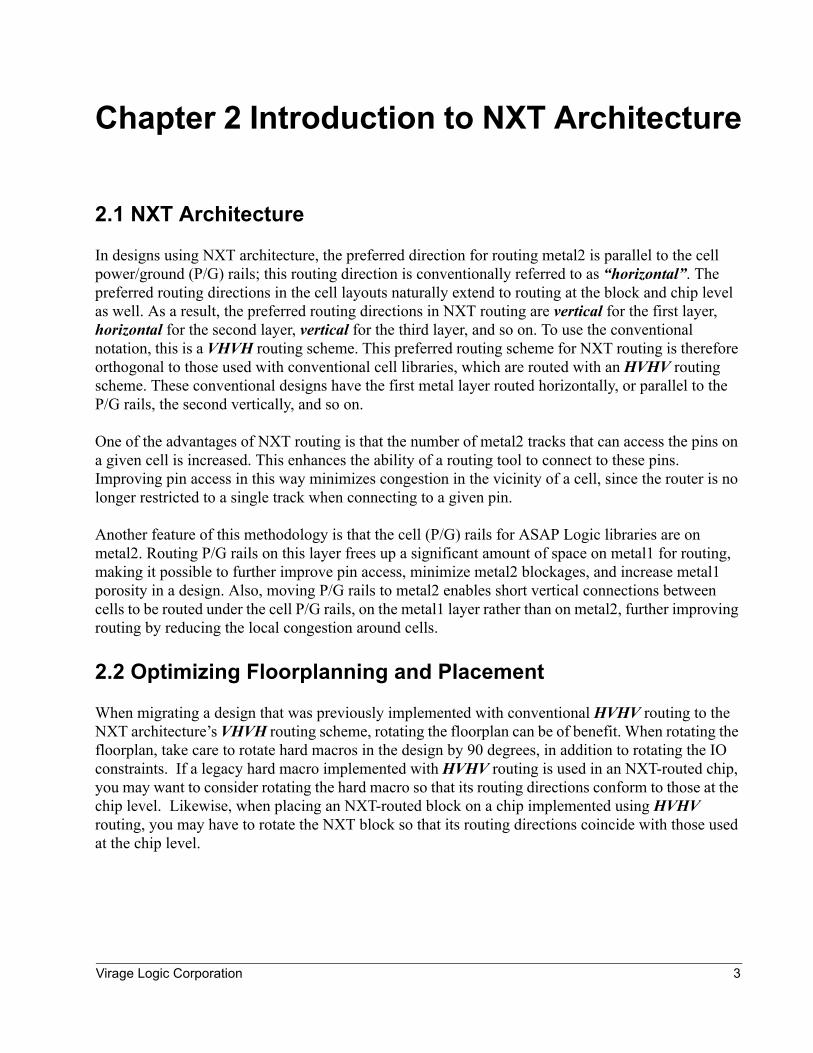
This is in contrast to the wide, infrequent, and clustered power straps that are the result of conventional HVHV routing. The power routing methodology in NXT routing ensures good pin access for cells placed under the vertical straps and minimizes the worst-case IR drop. Figure 2-1 shows the contrast between evenly spaced power strapping with thin straps on the one hand, and conventional clustered power strapping with wide straps on the other.
Figure 2-1
2.4 Optimizing Routing
ASAP Logic libraries are designed with VHVH routing style in mind. However, the routing direction for metal1 is assumed to be somewhat more flexible than other layers. As a result, if your router permits explicit control of wrong-way routing costs on different layers, you may consider using a smaller penalty for wrong-way routing on metal1 than on other metal layers.
NXT-style (metal3) power straps Conventional (metal2) power straps
4 Virage Logic Corporation
Chapter 3 Design Guidelines
This chapter provides you with some recommendations to keep in mind while using Virage Logic ASAP Logic libraries. It covers:
• Technology Setup• High-Level Architecture• Routing Directions and Power Grid Routing• Special Cells
3.1 Technology Setup
3.1.1 Setup for Cadence Design Systems Tools
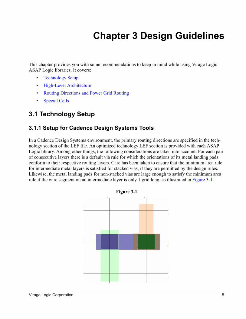
In a Cadence Design Systems environment, the primary routing directions are specified in the tech-nology section of the LEF file. An optimized technology LEF section is provided with each ASAP Logic library. Among other things, the following considerations are taken into account. For each pair of consecutive layers there is a default via rule for which the orientations of its metal landing pads conform to their respective routing layers. Care has been taken to ensure that the minimum area rule for intermediate metal layers is satisfied for stacked vias, if they are permitted by the design rules. Likewise, the metal landing pads for non-stacked vias are large enough to satisfy the minimum area rule if the wire segment on an intermediate layer is only 1 grid long, as illustrated in Figure 3-1.
Figure 3-1
Virage Logic Corporation 5
Design Guidelines
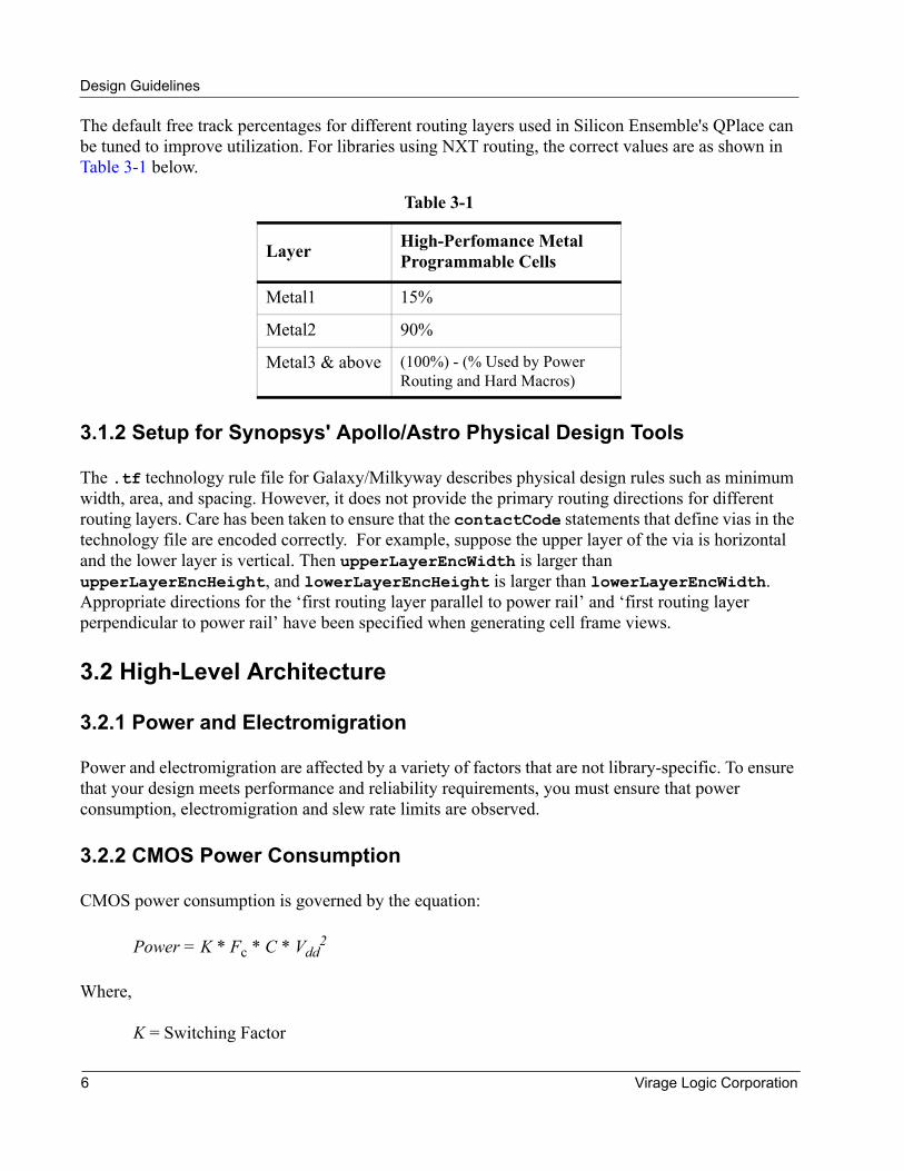
The default free track percentages for different routing layers used in Silicon Ensemble's QPlace can be tuned to improve utilization. For libraries using NXT routing, the correct values are as shown in Table 3-1 below.
3.1.2 Setup for Synopsys' Apollo/Astro Physical Design Tools
The .tf technology rule file for Galaxy/Milkyway describes physical design rules such as minimum width, area, and spacing. However, it does not provide the primary routing directions for different routing layers. Care has been taken to ensure that the contactCode statements that define vias in the technology file are encoded correctly. For example, suppose the upper layer of the via is horizontal and the lower layer is vertical. Then upperLayerEncWidth is larger than upperLayerEncHeight, and lowerLayerEncHeight is larger than lowerLayerEncWidth. Appropriate directions for the ‘first routing layer parallel to power rail’ and ‘first routing layer perpendicular to power rail’ have been specified when generating cell frame views.
3.2 High-Level Architecture
3.2.1 Power and Electromigration
Power and electromigration are affected by a variety of factors that are not library-specific. To ensure that your design meets performance and reliability requirements, you must ensure that power consumption, electromigration and slew rate limits are observed.
3.2.2 CMOS Power Consumption
CMOS power consumption is governed by the equation:
Power = K * Fc * C * Vdd2
Where,
K = Switching Factor
Table 3-1
Layer High-Perfomance Metal Programmable Cells
Metal1 15%
Metal2 90%
Metal3 & above (100%) - (% Used by Power Routing and Hard Macros)
6 Virage Logic Corporation
Design Guidelines
C = Load being Switched
Fc = Operating Frequency
Vdd = Operating Voltage
3.2.3 Operating Frequency
The operating frequency of a design directly affects its power consumption, with designs that operate at a higher frequency have a higher power consumption. The operating frequency of a design is generally is governed by its logic design. As such, the amount of power strapping used within a design will depend on the operating frequency.
ASAP Logic libraries are designed to ensure robust operation. While there is no limit to the maximum operating frequency, care must be taken to ensure that the electomigration limits of the technology are not exceeded. Please refer to Section 4.2, “Electrical Characteristics” on page 16, for further details.
3.2.4 Switching Factor
Switching factor, or how often the output of a cell switches relative to the frequency of operation, is a highly design-dependent parameter. ASAP Logic libraries contain power consumption information on a per-cell basis. With this informaton, you can use industry standard tools to calculate the switching factor for a cell or for a design using a rule of thumb, a heuristic statistical method or a simulation-driven method.
3.3 Routing Directions and Power Grid Routing
3.3.1 Routing Power Straps on Grid
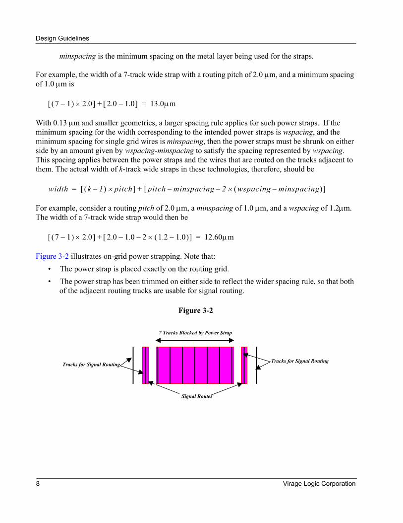
Power straps in NXT routing are more frequent to compensate for their narrower width. Off-grid straps can therefore potentially block a lot of tracks. Power straps must be routed on-grid; otherwise a k-track wide strap will block k+1 tracks. (The term ‘k tracks wide’ means that each strap occupies exactly k tracks.)
The actual width of a k-track wide strap is given by:
where
pitch is the routing pitch of the strap layer, and
width k 1–( ) pitch×[ ] pitch minspacing–[ ]+=
Virage Logic Corporation 7
Design Guidelines
minspacing is the minimum spacing on the metal layer being used for the straps.
For example, the width of a 7-track wide strap with a routing pitch of 2.0 µm, and a minimum spacing of 1.0 µm is
With 0.13 µm and smaller geometries, a larger spacing rule applies for such power straps. If the minimum spacing for the width corresponding to the intended power straps is wspacing, and the minimum spacing for single grid wires is minspacing, then the power straps must be shrunk on either side by an amount given by wspacing-minspacing to satisfy the spacing represented by wspacing. This spacing applies between the power straps and the wires that are routed on the tracks adjacent to them. The actual width of k-track wide straps in these technologies, therefore, should be
For example, consider a routing pitch of 2.0 µm, a minspacing of 1.0 µm, and a wspacing of 1.2µm. The width of a 7-track wide strap would then be
Figure 3-2 illustrates on-grid power strapping. Note that:• The power strap is placed exactly on the routing grid.• The power strap has been trimmed on either side to reflect the wider spacing rule, so that both
of the adjacent routing tracks are usable for signal routing.
Figure 3-2
7 1–( ) 2.0×[ ] 2.0 1.0–[ ]+ 13.0µm=
width k 1–( ) pitch×[ ] pitch minspacing– 2 wspacing minspacing–( )×–[ ]+=
7 1–( ) 2.0×[ ] 2.0 1.0– 2 1.2 1.0–( )×–[ ]+ 12.60µm=
Tracks for Signal Routing
Signal Routes
Tracks for Signal Routing
7 Tracks Blocked by Power Strap
8 Virage Logic Corporation
Design Guidelines
3.3.2 Routing Power Straps to Balance Signal Routing Resources
Virage Logic's ASAP Logic libraries are designed with a narrow (1- or 2-track wide) P/G rail within the cell layouts, but the cells are generally designed so that the rail widths can be increased by 1 or 2 additional tracks during block-level P&R. This enables the designer to customize the power distribution at the cell level as needed to minimize the risk of electromigration problems that can arise in cell libraries with narrower cell P/G rails. Consequently, ASAP Logic libraries can support wider spacing between successive vertical straps of the block- or chip-level power distribution grid.
Tuning your power strapping can have a significant impact on die size by reducing the congestion in the bottleneck direction. The demand for vertical and horizontal routing resources varies from netlist to netlist. In addition, demand for horizontal and vertical routing is dependent on the pin location. As a result of this, the horizontal or the vertical direction could become the bottleneck as the case may be. If the power strapping requirements are flexible, you can tune your power strapping to improve routing congestion. For example, if the vertical layers are more congested, you can increase the amount of horizontal power strapping and thereby reduce the amount of vertical strapping.
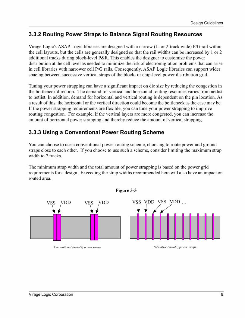
3.3.3 Using a Conventional Power Routing Scheme
You can choose to use a conventional power routing scheme, choosing to route power and ground straps close to each other. If you choose to use such a scheme, consider limiting the maximum strap width to 7 tracks.
The minimum strap width and the total amount of power strapping is based on the power grid requirements for a design. Exceeding the strap widths recommended here will also have an impact on routed area.
Figure 3-3
NXT-style (metal3) power straps Conventional (metal3) power straps
VDDVSS VDD VSS VDDVSS VDD VSS …
Virage Logic Corporation 9
Design Guidelines
3.4 Special Cells
3.4.1 Clock Driver Cell Usage
3.4.1.1 Clock Drivers, Symmetric Rise and Fall Cells
Clock and global signals need to maintain symmetric ramp times. Virage Logic provides cells with symmetric ramp times to be used as clock drivers.
These cells are named using the following scheme:
MDN_INV_S_<drive>
Symmetric rise and fall inverter.
MDN_BUF_S_<drive>
Symmetric rise and fall buffer.
For more details on cell naming convention, refer to Section 5.3, “Naming Conventions”
3.4.1.2 Clock Gating Cells
Power dissipation is becoming an increasingly bigger challenge in chip design as the integration level of circuits becomes large while clock frequencies also continue to increase. Virage Logic provides clock gating cells to help automate the process of power dissipation management.
10 Virage Logic Corporation
Design Guidelines
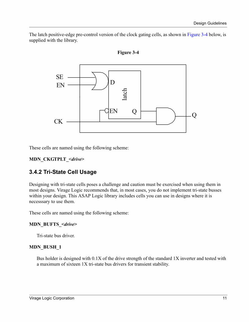
The latch positive-edge pre-control version of the clock gating cells, as shown in Figure 3-4 below, is supplied with the library.
Figure 3-4
These cells are named using the following scheme:
MDN_CKGTPLT_<drive>
3.4.2 Tri-State Cell Usage
Designing with tri-state cells poses a challenge and caution must be exercised when using them in most designs. Virage Logic recommends that, in most cases, you do not implement tri-state busses within your design. This ASAP Logic library includes cells you can use in designs where it is necesssary to use them.
These cells are named using the following scheme:
MDN_BUFTS_<drive>
Tri-state bus driver.
MDN_BUSH_1
Bus holder is designed with 0.1X of the drive strength of the standard 1X inverter and tested with a maximum of sixteen 1X tri-state bus drivers for transient stability.
CK la
tch
EN
D
Q
SE
Q
EN
Virage Logic Corporation 11
Design Guidelines
3.4.3 Delay Cell Usage
This ASAP Logic library includes delay cells to help you ensure that hold time requirements are met for difficult sections of the design. These delay cells have been designed with a delay which is a linear function of two-input NAND gate on which it is based.
These cells are named using the following scheme, and have the delay assumptions mentioned:
MDN_DEL_R<delayRatio>_<drive>
Delay cells are designed with relative delay in mind. The baseline delay uses as a reference a single (1X) drive 2-input NAND gate. The actual delay of the delay cell is the baseline delay multiplied by the delay ratio.
3.4.4 Filler Cell Usage
To ensure that your design passes DRC and LVS checks, it must include filler cells when you stream out GDS for final verification. You can insert filler cells into the design after all placement-related operations are complete, and before final signal routing is carried out.
The filler cells provided in this ASAP Logic library come in several sizes, and range from a cell covering a single unused placement site up to cells covering multiple unused sites. These filler cells are named according to the number of placement sites that they “fill”, using the following scheme:
MDN_FILL<sites>
The <sites> component of the name represents the number of grid positions the number of base cell widths covered by the cell, with the value of <sites> ranging from 1 to 256.
When adding filler cells to your design, start with the largest filler cell and work your way down to to the single-site filler cell. This will ensure that all the unused sites are filled with the smallest possible number of filler cell instances.
In addition, when using Silicon Ensemble, the variable
PLACE.LLC.IGNORE.LAYER.2
must be set to TRUE before you add filler cells, and set to FALSE once you have completed the fill operations. This is necessary in order to ensure proper gap filling within the array.
Here is an example sequence of Silicon Ensemble commands for filler cell insertion:
SET VARIABLE PLACE.LLC.IGNORE.LAYER.2 "TRUE";sroute addcell model "MDN_FILL256" prefix ......
12 Virage Logic Corporation
Design Guidelines
sroute addcell model "MDN_FILL2" prefix ...sroute addcell model "MDN_FILL1" prefix ...SET VARIABLE PLACE.LLC.IGNORE.LAYER.2 "FALSE";
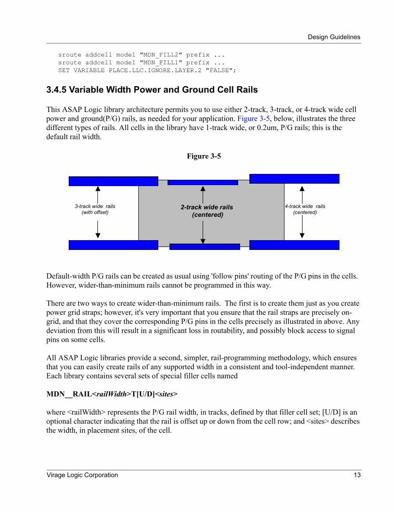
3.4.5 Variable Width Power and Ground Cell Rails
This ASAP Logic library architecture permits you to use either 2-track, 3-track, or 4-track wide cell power and ground(P/G) rails, as needed for your application. Figure 3-5, below, illustrates the three different types of rails. All cells in the library have 1-track wide, or 0.2um, P/G rails; this is the default rail width.
Figure 3-5
Default-width P/G rails can be created as usual using 'follow pins' routing of the P/G pins in the cells. However, wider-than-minimum rails cannot be programmed in this way.
There are two ways to create wider-than-minimum rails. The first is to create them just as you create power grid straps; however, it's very important that you ensure that the rail straps are precisely on-grid, and that they cover the corresponding P/G pins in the cells precisely as illustrated in above. Any deviation from this will result in a significant loss in routability, and possibly block access to signal pins on some cells.
All ASAP Logic libraries provide a second, simpler, rail-programming methodology, which ensures that you can easily create rails of any supported width in a consistent and tool-independent manner. Each library contains several sets of special filler cells named
MDN__RAIL<railWidth>T[U/D]<sites>
where <railWidth> represents the P/G rail width, in tracks, defined by that filler cell set; [U/D] is an optional character indicating that the rail is offset up or down from the cell row; and <sites> describes the width, in placement sites, of the cell.
4-track wide rails (centered)
3-track wide rails (with offset)
2-track wide rails (centered)
Virage Logic Corporation 13
Design Guidelines
This library contains two sets of these special filler cells, MDN_RAIL3TU* and MDN_RAIL3TD*. The first is used to define 2 or 4 track wide P/G rails of width equal to 1 track , the second is used to define 3-track wide rails, which must be offset from the top/bottom cell boundaries. Refer to Section 3.4.4, “Filler Cell Usage”, for a complete listing of the available rail filler cells. The P/G rails for the design can be routed as follows:
• After placing the hard macros and defining the standard cell rows, but before placing the cells, fill all cell rows with the rail cell set(s) corresponding to the desired P/G rail width, using the procedure for filler cells described in, Section 3.4.4, “Filler Cell Usage”, above. For 2- or 4-track wide rails, use the MDN_RAIL2T* or MDN_RAIL4T* rail cell set(s), respectively. For 3-track wide rails, fill all flipped rows with MDN_RAIL3TU*, and the remaining rows with MDN_RAIL3TD*.
• Create the cell P/G rails as usual, using the P/G pin widths of the MDN_RAIL* cell set with which you have filled the cell rows.
• Delete all MDN_RAIL* cells inserted above.• Perform cell placement and routing.
14 Virage Logic Corporation
Chapter 4 Library Characteristics
This chapter describes the characteristics of the ASAP High-Density Metal Programmable Library for TSMC 0.18um G FSG Standard Vt Process. It covers:
• Physical Characteristics• Electrical Characteristics• Electromigration Limit• Loading and Slew Rate
4.1 Physical Characteristics
Note: In order to achieve maximum routing density in this technology, most of the metal 1 input pins pass DRC only when the router connects the input pin at the chip level. Therefore, it is possible for DRC to fail if it is run on an individual cell, but this will not be a problem when using the library in a design.
Table 4-1 Physical Characteristics
Characteristic Value Comment
X Grid 0.56 µm No offset
Y Grid 0.56 µm No offset
Height 5.6 µm 10 Routing Tracks
Width Increments of 2.24µm (4 times the X-grid)
Symmetry Flipping about the Y axis is not allowed
Power Bus Width
0.42 µmIncreased to 0.70 µm for3-grid wide and 0.86 µmfor 4-grid wide bus
M2 - shared between cell rows on cell boundary
Virage Logic Corporation 15
Library Characteristics
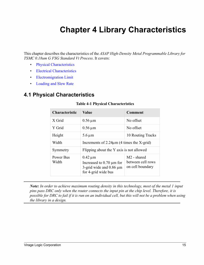
4.1.1 Example
Figure 4-1 Example Cell
4.2 Electrical Characteristics
All cells have been characterized for the following environmental conditions:
Extra care should be taken when deviating from these criteria as your design might not behave as documented here.
Table 4-2 Electrical Characteristics
Worst Case (SS) Slow process, 125 degree C, 1.62V
Typical Case (TT) Typical process, 25 degree C, 1.8V
Best Case (FF) Fast process, -40 degree C, 1.98V
16 Virage Logic Corporation
Library Characteristics
4.3 Electromigration Limit
The user must ensure that electromigration limits of the technology are not exceeded. ASAP Logic libraries are designed to ensure that the electromigration limit, for physical features in the cell, will be met if the following condition is satisfied.
Maximum cell output signal slew rate must be observed with the following relationship
4.4 Loading and Slew Rate
Excessive loading of signal nets can cause unpredictable timing behavior and excessive power consumption. ASAP Logic libraries are designed to operate within specific slew-rate and load ranges. Using cells in design scenarios that violate their operating ranges can cause problems for high toggle-rate and timing-critical nets.
ASAP Logic libraries avoid such problems by incorporating the following in their design:• Cell are designed with P/G rail fidelity in mind, taking electromigration into account for high-
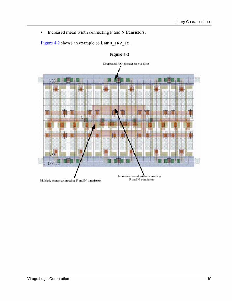
drive and clock-related cells: • P/G contact-to-via ratio set to 1:1.
This ensures that the via does not become an electromigration bottleneck for high-speed designs. Note that within a given cell, this requires that there be twice as many vias as con-tacts, since vias are on the top and bottom cell boundaries, and therefore potentially shared between cells in vertically-adjacent rows.• Metal-segment widths increased as needed to meet electromigration specs.
This ensures that metal segments that experience pulsed-DC current will not fail at the maxi-mum frequency and load conditions specified for the library.
Figure 4-2 shows an example cell, MDN_INV_16, which illustrates these features.• Libraries undergo correct-by-construction cell characterization, which limits the maximum
slew across the entire library.
The maximum load for each output pin is determined from the maximum slew.
The maximum slew, which varies for each PVT corner, is defined to be the output slew of a 1X inverter driving 64 1X inverters.
maxSlew 1 switchingFactor⁄( )x 1 frequency⁄( )x0.10[ ]≤
Virage Logic Corporation 17
Library Characteristics
Here are the maximum slews for this library (measured between 10% and 90% of VDD)::
With the maximum slew rate set, the only variable factors are the operating frequency and switching factor, which you can control.
• Cell architecture designed for power rail fidelity to ensure that cell design takes electromigration into account for high drive and clock-related cells:• Power contact-to-via ratio set to 1:1.
This ensures that the via does not become an electromigration bottleneck for high-speed design.
Table 4-3 Maximum Slew Table
PVT Rise(ps)
SS 3589
TT 2504
FF 1832
18 Virage Logic Corporation
Library Characteristics
• Increased metal width connecting P and N transistors.
Figure 4-2 shows an example cell, MDN_INV_12.
Figure 4-2
Virage Logic Corporation 19

Library Characteristics
20 Virage Logic Corporation
Chapter 5 Datasheets
ASAP Logic libraries are designed to optimize the metrics for area, power, and routability of ASIC designs. The ASAP High-Density Metal Programmable Library for TSMC 0.18um G FSG Standard Vt Process contains 474 cells (excluding filler types) and 126 functions, as well as a range of filler cells.
This chapter provides you with data on the library and the cells it contains. It includes:• Cell Selection Philosophy• Cell Function Summary• Naming Conventions• Datasheets
5.1 Cell Selection Philosophy
5.1.1 Synthesis Friendly
ASAP Logic libraries have functional continuity, which is essential for optimal technology mapping during logic synthesis. This requires that whenever a complex gate is available in the library, gates for its Boolean sub-expressions are also available. This library contains
• Cells for different types of AOI, OAI, AO, and OA functions which can be implemented more efficiently as a single cell than a combination of individual AND, OR, NAND, NOR, INV gates.
• Several gates with bubble (inverted) inputs which can be implemented more efficiently as a single gate than using a combination of a simple gate with inverters to invert individual inputs.
• No complex flip-flops such as Set-Reset and JK, since modern synthesis tools prefer to build the equivalent logic with simpler building blocks.
• Numerous drive-strengths for frequently used functions to help with timing, as well as to further minimize power consumption.
• Flip-flops and latches with many drive-strengths to help with timing.
5.1.2 Place and Route Friendly
Better pin access is a basic feature of all ASAP Logic libraries. Other features of these libraries that produce much better place and route results, include
• A minimum number of large cells, such as 8-bit counters, 4-bit latches. The absence of such
Virage Logic Corporation 21
Datasheets
gates enables better optimization during placement, and minimizes perturbations when handling engineering change orders (ECOs) or performing netlist changes for timing correction.
• A minimum number of gates (other than buffers and inverters) with very high drive-strengths, since they tend to encourage high fan-out nets during synthesis, causing wiring congestion. When such gates are required for performance considerations, their use is not recommended for initial random-logic synthesis.
• Carefully optimized pin-placements for all library cells, to provide maximum pin access, and consequently minimum local congestion.
• A minimal amount of metal2 blockage. This minimizes restrictions on cell placement, leading to higher utilization and lower local congestion.
• Carefully adjusted wiring pitches for all metal layers, to optimize overall chip area, routability and wire length.
5.1.3 Optimized Performance and Power
The ASAP Logic library provides you with a range of drive strength options for the more frequently used cells, such as inverters and buffers.
5.2 Cell Function Summary
Your ASAP Logic library consists of cells with a wide range of functions to fulfill your design needs:• Standard combinational logic gates. Such as AND, OR, NAND, NOR.• Standard combinational logic gates with inverted inputs.• Exclusive-OR and exclusive-NOR.• MUX, adders and comparators.• AOI (and-or-inverted) and OAI (or-and-inverted) gates, and their counterparts with bubble
inputs.• AO (AND-OR) and OA (OR-AND) gates.• Inverters, buffers, and delay elements, tri-state buffers, and clock buffers.• Numerous latches and flip-flops, including scan flip-flops.• High performance cells for use with Synopsys Module Compiler.
22 Virage Logic Corporation
Datasheets
5.3 Naming Conventions
5.3.1 Cell Naming Syntax
<prefix>_<baseName>[_<extension>][_<drive>]
<prefix>
This is a three-letter prefix identifying the type of library the cell is a part of as well as the Vt cor-ner.
<baseName>
This is an alphanumeric string conveying the function in commonly used form.
<extension>
This optional extension to the name appears where the general function of the cell is the same but the specific implementation requires a unique topology or other consideration.
<drive>
This optional suffix gives the drive strength, the driving capability of the cell, in the number for-mat. Fractional numbers are expressed as <N1>P<N2>, where "P" represents the decimal point. For example, a 0.5X drive cell would have a drive suffix of "0P5"; a 1.75X drive cell would have a drive suffix of "1P75"; and so on.
5.3.2 Examples
A cell with the name
MDN_INV_S_1
is a standard cell symmetric rise and fall inverter with a 1x drive strength.
Virage Logic Corporation 23
Datasheets
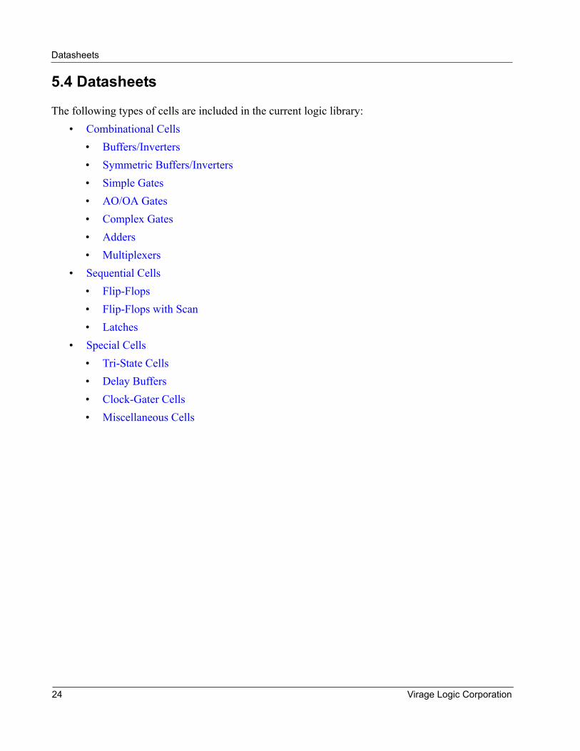
5.4 Datasheets
The following types of cells are included in the current logic library:• Combinational Cells
• Buffers/Inverters• Symmetric Buffers/Inverters• Simple Gates• AO/OA Gates• Complex Gates• Adders• Multiplexers
• Sequential Cells• Flip-Flops• Flip-Flops with Scan• Latches
• Special Cells• Tri-State Cells• Delay Buffers• Clock-Gater Cells• Miscellaneous Cells
24 Virage Logic Corporation
Datasheets
• Filler Cells
The following sub-sections provide you a list of the cells included in this library. You can click on the name of each cell to view the Datasheet for it.
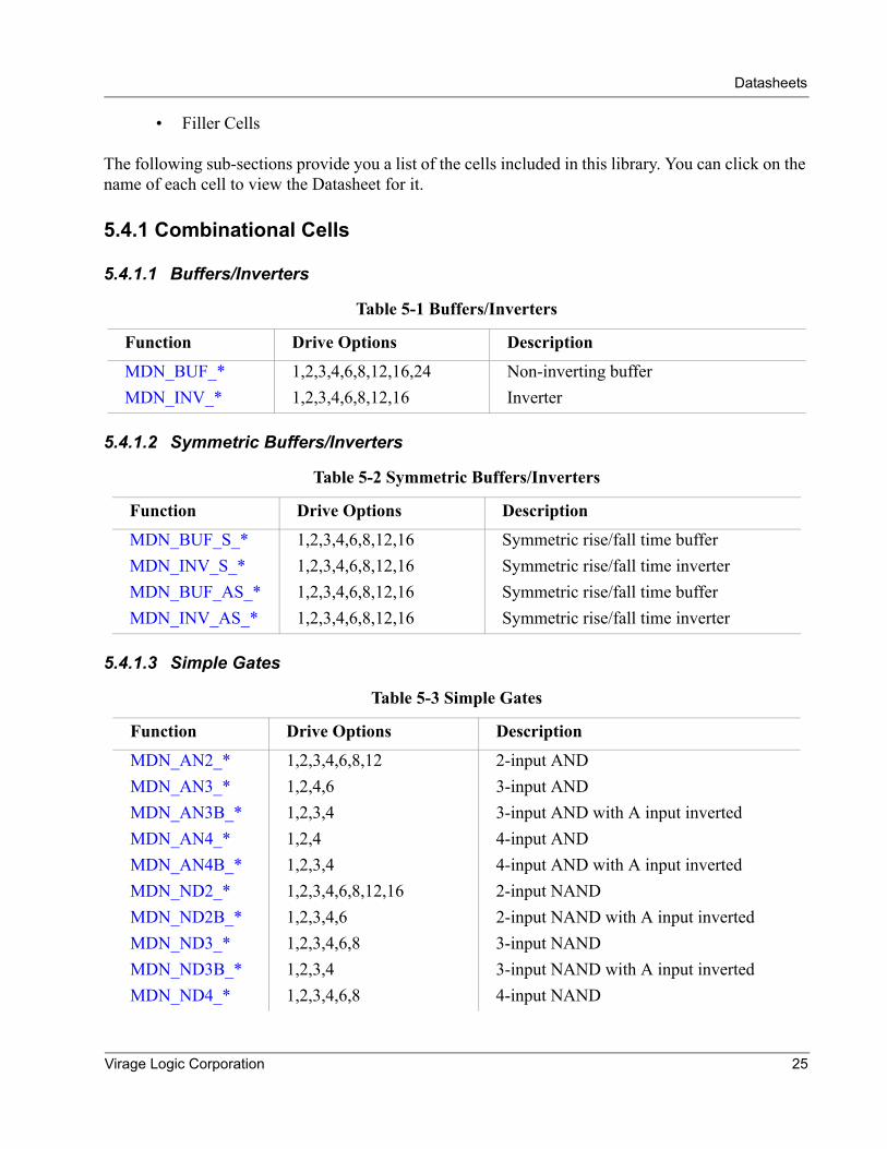
5.4.1 Combinational Cells
5.4.1.1 Buffers/Inverters
5.4.1.2 Symmetric Buffers/Inverters
5.4.1.3 Simple Gates
Table 5-1 Buffers/Inverters
Function Drive Options Description
MDN_BUF_* 1,2,3,4,6,8,12,16,24 Non-inverting bufferMDN_INV_* 1,2,3,4,6,8,12,16 Inverter
Table 5-2 Symmetric Buffers/Inverters
Function Drive Options Description
MDN_BUF_S_* 1,2,3,4,6,8,12,16 Symmetric rise/fall time bufferMDN_INV_S_* 1,2,3,4,6,8,12,16 Symmetric rise/fall time inverterMDN_BUF_AS_* 1,2,3,4,6,8,12,16 Symmetric rise/fall time bufferMDN_INV_AS_* 1,2,3,4,6,8,12,16 Symmetric rise/fall time inverter
Table 5-3 Simple Gates
Function Drive Options Description
MDN_AN2_* 1,2,3,4,6,8,12 2-input ANDMDN_AN3_* 1,2,4,6 3-input ANDMDN_AN3B_* 1,2,3,4 3-input AND with A input invertedMDN_AN4_* 1,2,4 4-input ANDMDN_AN4B_* 1,2,3,4 4-input AND with A input invertedMDN_ND2_* 1,2,3,4,6,8,12,16 2-input NANDMDN_ND2B_* 1,2,3,4,6 2-input NAND with A input invertedMDN_ND3_* 1,2,3,4,6,8 3-input NANDMDN_ND3B_* 1,2,3,4 3-input NAND with A input invertedMDN_ND4_* 1,2,3,4,6,8 4-input NAND
Virage Logic Corporation 25
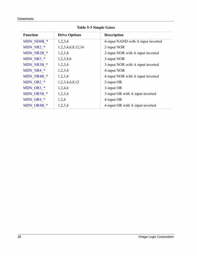
Datasheets
MDN_ND4B_* 1,2,3,4 4-input NAND with A input invertedMDN_NR2_* 1,2,3,4,6,8,12,16 2-input NORMDN_NR2B_* 1,2,3,4 2-input NOR with A input invertedMDN_NR3_* 1,2,3,4,6 3-input NORMDN_NR3B_* 1,2,3,4 3-input NOR with A input invertedMDN_NR4_* 1,2,3,4 4-input NORMDN_NR4B_* 1,2,3,4 4-input NOR with A input invertedMDN_OR2_* 1,2,3,4,6,8,12 2-input ORMDN_OR3_* 1,2,4,6 3-input ORMDN_OR3B_* 1,2,3,4 3-input OR with A input invertedMDN_OR4_* 1,2,4 4-input ORMDN_OR4B_* 1,2,3,4 4-input OR with A input inverted
Table 5-3 Simple Gates
Function Drive Options Description
26 Virage Logic Corporation
Datasheets
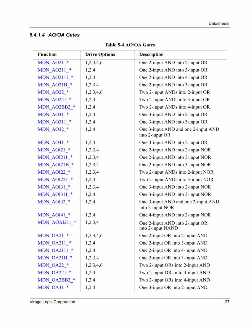
5.4.1.4 AO/OA Gates
Table 5-4 AO/OA Gates
Function Drive Options Description
MDN_AO21_* 1,2,3,4,6 One 2-input AND into 2-input ORMDN_AO211_* 1,2,4 One 2-input AND into 3-input ORMDN_AO2111_* 1,2,4 One 2-input AND into 4-input ORMDN_AO21B_* 1,2,3,4 One 2-input AND into 3-input ORMDN_AO22_* 1,2,3,4,6 Two 2-input ANDs into 2-input ORMDN_AO221_* 1,2,4 Two 2-input ANDs into 3-input ORMDN_AO2BB2_* 1,2,4 Two 2-input ANDs into 4-input ORMDN_AO31_* 1,2,4 One 3-input AND into 2-input ORMDN_AO311_* 1,2,4 One 3-input AND into 3-input ORMDN_AO32_* 1,2,4 One 3-input AND and one 2-input AND
into 2-input ORMDN_AO41_* 1,2,4 One 4-input AND into 2-input ORMDN_AOI21_* 1,2,3,4 One 2-input AND into 2-input NORMDN_AOI211_* 1,2,3,4 One 2-input AND into 3-input NORMDN_AOI21B_* 1,2,3,4 One 2-input AND into 3-input NORMDN_AOI22_* 1,2,3,4 Two 2-input ANDs into 2-input NORMDN_AOI221_* 1,2,4 Two 2-input ANDs into 3-input NORMDN_AOI31_* 1,2,3,4 One 3-input AND into 2-input NORMDN_AOI311_* 1,2,4 One 3-input AND into 3-input NORMDN_AOI32_* 1,2,4 One 3-input AND and one 2-input AND
into 2-input NORMDN_AOI41_* 1,2,4 One 4-input AND into 2-input NORMDN_AOAI211_* 1,2,3,4 One 2-input AND into 2-input OR
into 2-input NANDMDN_OA21_* 1,2,3,4,6 One 2-input OR into 2-input ANDMDN_OA211_* 1,2,4 One 2-input OR into 3-input ANDMDN_OA2111_* 1,2,4 One 2-input OR into 4-input ANDMDN_OA21B_* 1,2,3,4 One 2-input OR into 3-input ANDMDN_OA22_* 1,2,3,4,6 Two 2-input ORs into 2-input ANDMDN_OA221_* 1,2,4 Two 2-input ORs into 3-input ANDMDN_OA2BB2_* 1,2,4 Two 2-input ORs into 4-input ANDMDN_OA31_* 1,2,4 One 3-input OR into 2-input AND
Virage Logic Corporation 27
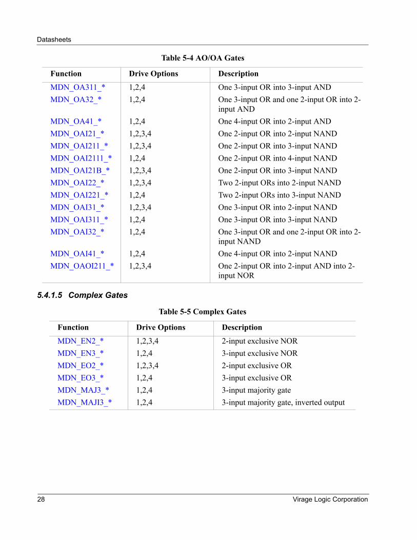
Datasheets
5.4.1.5 Complex Gates
MDN_OA311_* 1,2,4 One 3-input OR into 3-input ANDMDN_OA32_* 1,2,4 One 3-input OR and one 2-input OR into 2-
input ANDMDN_OA41_* 1,2,4 One 4-input OR into 2-input ANDMDN_OAI21_* 1,2,3,4 One 2-input OR into 2-input NANDMDN_OAI211_* 1,2,3,4 One 2-input OR into 3-input NANDMDN_OAI2111_* 1,2,4 One 2-input OR into 4-input NANDMDN_OAI21B_* 1,2,3,4 One 2-input OR into 3-input NANDMDN_OAI22_* 1,2,3,4 Two 2-input ORs into 2-input NANDMDN_OAI221_* 1,2,4 Two 2-input ORs into 3-input NANDMDN_OAI31_* 1,2,3,4 One 3-input OR into 2-input NANDMDN_OAI311_* 1,2,4 One 3-input OR into 3-input NANDMDN_OAI32_* 1,2,4 One 3-input OR and one 2-input OR into 2-
input NANDMDN_OAI41_* 1,2,4 One 4-input OR into 2-input NANDMDN_OAOI211_* 1,2,3,4 One 2-input OR into 2-input AND into 2-
input NOR
Table 5-5 Complex Gates
Function Drive Options Description
MDN_EN2_* 1,2,3,4 2-input exclusive NORMDN_EN3_* 1,2,4 3-input exclusive NORMDN_EO2_* 1,2,3,4 2-input exclusive ORMDN_EO3_* 1,2,4 3-input exclusive ORMDN_MAJ3_* 1,2,4 3-input majority gateMDN_MAJI3_* 1,2,4 3-input majority gate, inverted output
Table 5-4 AO/OA Gates
Function Drive Options Description
28 Virage Logic Corporation
Datasheets
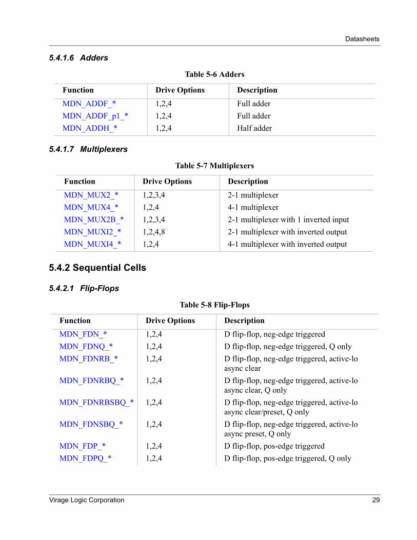
5.4.1.6 Adders
5.4.1.7 Multiplexers
5.4.2 Sequential Cells
5.4.2.1 Flip-Flops
Table 5-6 Adders
Function Drive Options Description
MDN_ADDF_* 1,2,4 Full adderMDN_ADDF_p1_* 1,2,4 Full adderMDN_ADDH_* 1,2,4 Half adder
Table 5-7 Multiplexers
Function Drive Options Description
MDN_MUX2_* 1,2,3,4 2-1 multiplexerMDN_MUX4_* 1,2,4 4-1 multiplexerMDN_MUX2B_* 1,2,3,4 2-1 multiplexer with 1 inverted inputMDN_MUXI2_* 1,2,4,8 2-1 multiplexer with inverted outputMDN_MUXI4_* 1,2,4 4-1 multiplexer with inverted output
Table 5-8 Flip-Flops
Function Drive Options Description
MDN_FDN_* 1,2,4 D flip-flop, neg-edge triggeredMDN_FDNQ_* 1,2,4 D flip-flop, neg-edge triggered, Q onlyMDN_FDNRB_* 1,2,4 D flip-flop, neg-edge triggered, active-lo
async clearMDN_FDNRBQ_* 1,2,4 D flip-flop, neg-edge triggered, active-lo
async clear, Q onlyMDN_FDNRBSBQ_* 1,2,4 D flip-flop, neg-edge triggered, active-lo
async clear/preset, Q onlyMDN_FDNSBQ_* 1,2,4 D flip-flop, neg-edge triggered, active-lo
async preset, Q onlyMDN_FDP_* 1,2,4 D flip-flop, pos-edge triggeredMDN_FDPQ_* 1,2,4 D flip-flop, pos-edge triggered, Q only
Virage Logic Corporation 29
Datasheets
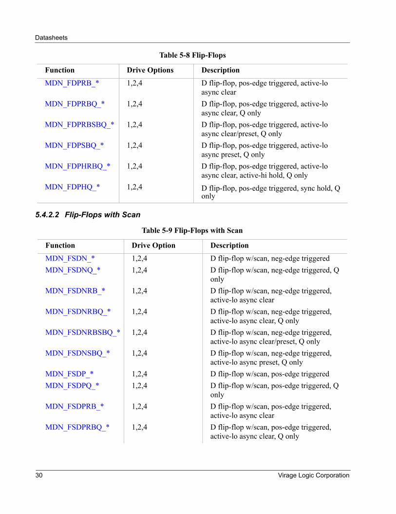
5.4.2.2 Flip-Flops with Scan
MDN_FDPRB_* 1,2,4 D flip-flop, pos-edge triggered, active-lo async clear
MDN_FDPRBQ_* 1,2,4 D flip-flop, pos-edge triggered, active-lo async clear, Q only
MDN_FDPRBSBQ_* 1,2,4 D flip-flop, pos-edge triggered, active-lo async clear/preset, Q only
MDN_FDPSBQ_* 1,2,4 D flip-flop, pos-edge triggered, active-lo async preset, Q only
MDN_FDPHRBQ_* 1,2,4 D flip-flop, pos-edge triggered, active-lo async clear, active-hi hold, Q only
MDN_FDPHQ_* 1,2,4 D flip-flop, pos-edge triggered, sync hold, Qonly
Table 5-9 Flip-Flops with Scan
Function Drive Option Description
MDN_FSDN_* 1,2,4 D flip-flop w/scan, neg-edge triggeredMDN_FSDNQ_* 1,2,4 D flip-flop w/scan, neg-edge triggered, Q
onlyMDN_FSDNRB_* 1,2,4 D flip-flop w/scan, neg-edge triggered,
active-lo async clearMDN_FSDNRBQ_* 1,2,4 D flip-flop w/scan, neg-edge triggered,
active-lo async clear, Q onlyMDN_FSDNRBSBQ_* 1,2,4 D flip-flop w/scan, neg-edge triggered,
active-lo async clear/preset, Q onlyMDN_FSDNSBQ_* 1,2,4 D flip-flop w/scan, neg-edge triggered,
active-lo async preset, Q onlyMDN_FSDP_* 1,2,4 D flip-flop w/scan, pos-edge triggeredMDN_FSDPQ_* 1,2,4 D flip-flop w/scan, pos-edge triggered, Q
onlyMDN_FSDPRB_* 1,2,4 D flip-flop w/scan, pos-edge triggered,
active-lo async clearMDN_FSDPRBQ_* 1,2,4 D flip-flop w/scan, pos-edge triggered,
active-lo async clear, Q only
Table 5-8 Flip-Flops
Function Drive Options Description
30 Virage Logic Corporation
Datasheets
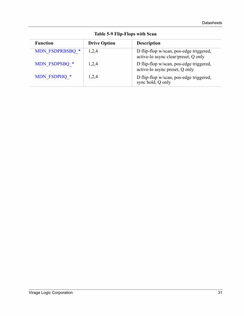
MDN_FSDPRBSBQ_* 1,2,4 D flip-flop w/scan, pos-edge triggered, active-lo async clear/preset, Q only
MDN_FSDPSBQ_* 1,2,4 D flip-flop w/scan, pos-edge triggered, active-lo async preset, Q only
MDN_FSDPHQ_* 1,2,4 D flip-flop w/scan, pos-edge triggered,sync hold, Q only
Table 5-9 Flip-Flops with Scan
Function Drive Option Description
Virage Logic Corporation 31
Datasheets
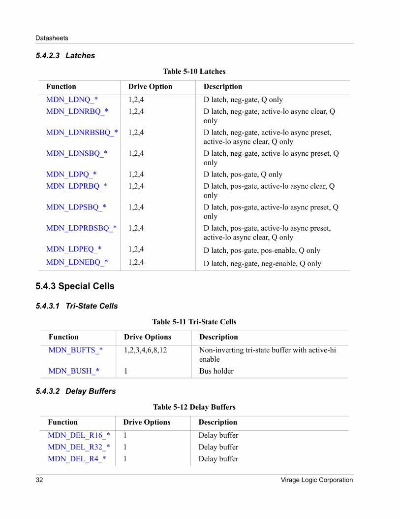
5.4.2.3 Latches
5.4.3 Special Cells
5.4.3.1 Tri-State Cells
5.4.3.2 Delay Buffers
Table 5-10 Latches
Function Drive Option Description
MDN_LDNQ_* 1,2,4 D latch, neg-gate, Q onlyMDN_LDNRBQ_* 1,2,4 D latch, neg-gate, active-lo async clear, Q
onlyMDN_LDNRBSBQ_* 1,2,4 D latch, neg-gate, active-lo async preset,
active-lo async clear, Q onlyMDN_LDNSBQ_* 1,2,4 D latch, neg-gate, active-lo async preset, Q
onlyMDN_LDPQ_* 1,2,4 D latch, pos-gate, Q onlyMDN_LDPRBQ_* 1,2,4 D latch, pos-gate, active-lo async clear, Q
onlyMDN_LDPSBQ_* 1,2,4 D latch, pos-gate, active-lo async preset, Q
onlyMDN_LDPRBSBQ_* 1,2,4 D latch, pos-gate, active-lo async preset,
active-lo async clear, Q onlyMDN_LDPEQ_* 1,2,4 D latch, pos-gate, pos-enable, Q onlyMDN_LDNEBQ_* 1,2,4 D latch, neg-gate, neg-enable, Q only
Table 5-11 Tri-State Cells
Function Drive Options Description
MDN_BUFTS_* 1,2,3,4,6,8,12 Non-inverting tri-state buffer with active-hi enable
MDN_BUSH_* 1 Bus holder
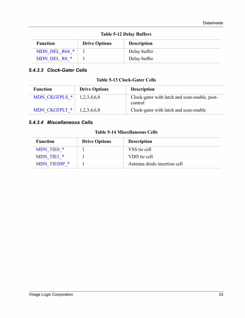
Table 5-12 Delay Buffers
Function Drive Options Description
MDN_DEL_R16_* 1 Delay bufferMDN_DEL_R32_* 1 Delay bufferMDN_DEL_R4_* 1 Delay buffer
32 Virage Logic Corporation
Datasheets
5.4.3.3 Clock-Gater Cells
5.4.3.4 Miscellaneous Cells
MDN_DEL_R64_* 1 Delay bufferMDN_DEL_R8_* 1 Delay buffer
Table 5-13 Clock-Gater Cells
Function Drive Options Description
MDN_CKGTPLS_* 1,2,3,4,6,8 Clock-gater with latch and scan-enable, post-control
MDN_CKGTPLT_* 1,2,3,4,6,8 Clock-gater with latch and scan-enable
Table 5-14 Miscellaneous Cells
Function Drive Options Description
MDN_TIE0_* 1 VSS tie cellMDN_TIE1_* 1 VDD tie cellMDN_TIEDIP_* 1 Antenna diode insertion cell
Table 5-12 Delay Buffers
Function Drive Options Description
Virage Logic Corporation 33
Datasheets
34 Virage Logic Corporation
Chapter 6 Characterization Methodology
Each cell provided as part of the ASAP Logic library design kit is characterized using a netlist extracted from the cell layout, and the characterization tool suite from Cell Builder. The following parameters are characterized:
1. Input pin capacitance2. Combinational pin-to-pin delays3. Output pin transition times4. Dynamic (switching) power dissipation5. Timing check constraints6. Steady-state power dissipation.
A characterization database is generated for these parameters over a pre-determined set of environmental conditions, usually comprised of "worst case", "typical", and "best case" corners. Additional corners are included as needed. This database is used as the basis for creating synthesis, simulation, and timing models for various EDA tools.
6.1 Input Pin Capacitance
The cell pin being characterized is treated as a simple capacitive load and the rise and fall delays to charge or discharge this ‘capacitor’ are measured by simulation. These measured delays are then matched to actual pure-capacitive equivalent delays.
6.2 Combinational Pin-to-Pin Delays
Combinational cell delays are obtained for each distinct input-pin to output-pin path, by adding a load to the output pin, applying a transition on the input pin, and measuring the corresponding delay through a SPICE circuit simulator. This process is repeated for all desired combinations of input transitions and output loads. In order to model the delays as accurately as possible, the transition applied to the input pin is a realistic CMOS waveform, obtained by passing a piecewise-linear (PWL) transition through a pre-buffer circuit. This pre-buffer is usually one of the non-inverting buffer cells from the library itself.
6.3 Output Pin Transition Times
During the measurement of combinational delays, as described in 6.1.2, the rise/fall transition times on the output are also captured for each combination of input transitions and output loads.
Virage Logic Corporation 35
Characterization Methodology
6.4 Dynamic Power Dissipation
The power dissipated by a cell during state transitions is obtained by measuring the switching current through the circuit, from VDD to VSS, and multiplying by the rail-to-rail voltage difference. This switching current is measured during each of the pin-to-pin delay characterizations, as described in Section 6.2, “Combinational Pin-to-Pin Delays” on page 35, above, as well as for input transitions which cause an internal node transition but have no corresponding output transition.
6.5 Timing Check Constraints
A reference simulation is performed for a given clock-to-Q transistion, and then the clock and data edges (or two clock edges, in the case of minimum pulse width) are moved progressively closer together until failure (that is, the clock-to-Q transition increases in delay by prescribed amount prior to complete failure). The resulting time between the two edges is the setup, hold, or MPW. This process is repeated for all desired data-input-slope/clock-input-slope combinations.
6.6 Steady-State Power Dissipation
The steady-state, or static, power dissipated by a cell in a given state is determined by measuring the current through the circuit, from VDD to VSS, and multiplying by the rail-to-rail voltage difference. The current is only measured once the circuit has fully transitioned into that state, and all the nodes have settled. This process is repeated for all the distinct states of the circuit.
36 Virage Logic Corporation
Chapter 7 Modeling Methodology andValidation
All of the models provided in the ASAP Logic library design kit are designed to provide accurate representations of the design and performance of each cell to all of the various EDA tools used in the design process, while at the same time optimizing the runtime performance in each of these tools.
The EDA views provided as standard deliverables with this ASAP Logic library are listed in “Standard List of Models”, below. To request a custom set of views, please contact Virage Logic as described in Section 1.4, “Technical Assistance” on page 2.
7.1 Standard List of Models
The EDA views delivered with the standard ASAP Logic library design kit are listed below. Please refer to the file named release.txt shipped with this product for the specific versions of the EDA views delivered to you.
• GDSII• LVS• LEF• Verilog• VHDL (VITAL-1 compliant)• Synopsys Galaxy/Milkyway database (frames and CLF for each PVT corner)• Synopsys Liberty DB (one per PVT corner)• Synopsys Physical Liberty DB• TLF (one per PVT corner)• Mentor Graphics Fastscan ATPG models
7.2 Quality Assurance Methodology
Each ASAP Logic product undergoes a variety of tests, focusing on accuracy, consistency, and usability in a wide variety of proprietary and industry tools. Unit level cell tests include Layout-versus-Schematic (LVS), Design Rule Checking (DRC), architectural checks that ensure proper design, logic functionality and equivalency, and characterization accuracy. A variety of leading industry design and analysis tools are run with these libraries and the results compared to each other to ensure consistent and accurate interpretation of the various library views. A sample RTL->GDS
Virage Logic Corporation 37
Modeling Methodology
design methodology is run to ensure successful completion of a tape-out flow. This flow is almost identical to the sample flow included with each library.
All library validation is audited and documented in accordance with ISO9000 requirements.
Coverage on the EDA views listed in “Standard List of Models” is obtained with the following:
Library Construction Checks
Library Construction Checks are used to validate that the design is accurately represented in each EDA model.
Library View Cross-Checking
Library View Cross-Checking is performed to ensure that the information is consistent across the various model types.
Tool vs. Golden Data Checks
Tool vs. Golden Data Checks are used to correlate each EDA tool with the design area.
Tool vs. Tool Checks
Tool vs. Tool Checks are used to verify consistency between two analysis tools.
Methodology Checks
Methodology Checks are used in verifying the end-user flow and proactively identifying any problems with usage.
7.3 Explanation of Physical Models
Physical models come in two flavors: full layout and cell abstract. Full layouts are required in the final steps of design verification, while cell abstracts are used by place-and-route tools.
7.3.1 Full Layout Database
The full layout database contains all tapeout layers for all cells. These views are required for final design verification, when they are merged in with the routing geometries to run full-layer DRC, LVS, and other checks.
The full layout database in this library is provided both in GDSII format and in the Synopsys Galaxy/Milkyway "CEL" format.
38 Virage Logic Corporation

Modeling Methodology
Figure 7-1, below, shows an example of the full layout database for a 2-to-1 multiplexer cell.
Figure 7-1
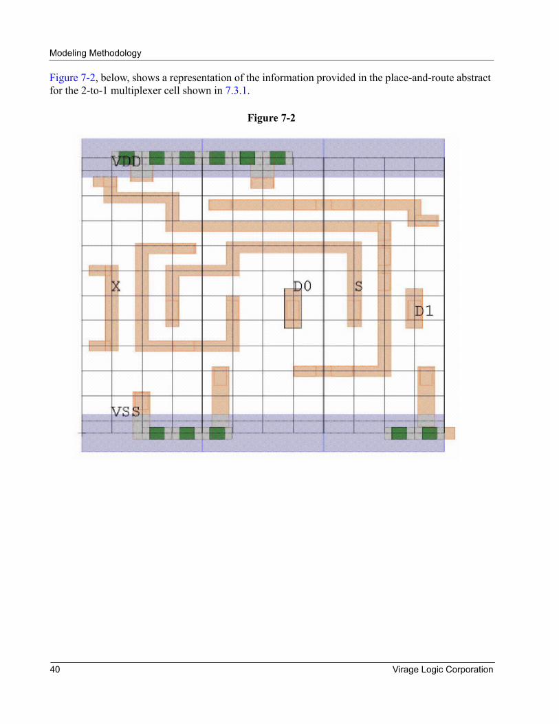
7.3.2 Cell Place-and-Route Abstract Model
Cell place-and-route abstract models, variously referred to as LEF, frame, phantom, or footprint, contain only the layout data required by the place-and-route tools. This data generally consists of the cell size and bounding box, the location and layer information for pins and blockages, pin names, and pin antenna information.
The place-and-route abstracts in this library are provided both in Cadence LEF format and in the Synopsys Milkyway "frame" format.
Virage Logic Corporation 39
Modeling Methodology
Figure 7-2, below, shows a representation of the information provided in the place-and-route abstract for the 2-to-1 multiplexer cell shown in 7.3.1.
Figure 7-2
40 Virage Logic Corporation