Embed Size (px)
Citation preview

20 IEEE CIRCUITS AND SYSTEMS MAGAZINE 1531-636X/09/$26.00©2009 IEEE THIRD QUARTER 2009
Feature
Digital Object Identifier 10.1109/MCAS.2009.933855
Routing for Manufacturability and Reliability Huang-Yu Chen
and Yao-Wen Chang
AbstractAs IC process geometries scale down to the nanometer ter-ritory, industry faces severe challenges of manufacturing limitations. To guarantee high yield and reliability, routing for manufacturability and reliability has played a pivotal role in resolution and thus yield enhancement for the imperfect manufacturing process. In this article, we introduce major routing challenges arising from nanometer process, survey key existing techniques for handling the challenges, and pro-vide some future research directions in routing for manufac-turability and reliability.
© COREL
Authorized licensed use limited to: CityU. Downloaded on September 10, 2009 at 08:28 from IEEE Xplore. Restrictions apply.
THIRD QUARTER 2009 IEEE CIRCUITS AND SYSTEMS MAGAZINE 21
Huang-Yu Chen is with the Graduate Institute of Electronics Engineering, and Yao-Wen Chang is with Department of Electrical Engineering, National
Taiwan University, Taipei, Taiwan. E-mails: [email protected]; [email protected].
I. Introduction
s the process geometries scale down to the nano-
meter territory, the IC industry faces severe
challenges in manufacturability and reliability.
Among these challenges, optical proximity correction
(OPC) and chemical-mechanical polishing (CMP) are
current major issues for manufacturability, and anten-
na effect avoidance and double-via insertion are often
adopted for reliability enhancement. Those issues are
often tackled at the post-layout stage. Nevertheless,
with the fast-growing design complexity, it is desirable
to handle these issues earlier at the routing stage to
provide higher flexibility for the optimization. Conse-
quently, we shall focus our discussions on routing for
these challenges.
II. Routing for Manufacturability
For manufacturability, OPC and CMP are two most im-
portant concerns for modern chip designs. The former
adds or subtracts feature patterns to a mask to enhance
the layout resolution and thus the printability of the
mask patterns on the wafer, while the latter improves
layout uniformity and chip planarization to achieve
higher manufacturing yield.
A. OPC-Aware RoutingWe shall first briefly introduce the manufacturing pro-
cess. The process uses an optical lithography system
and goes through many cycles of processing, each of
which consists of two major steps: exposure followed
by etching.
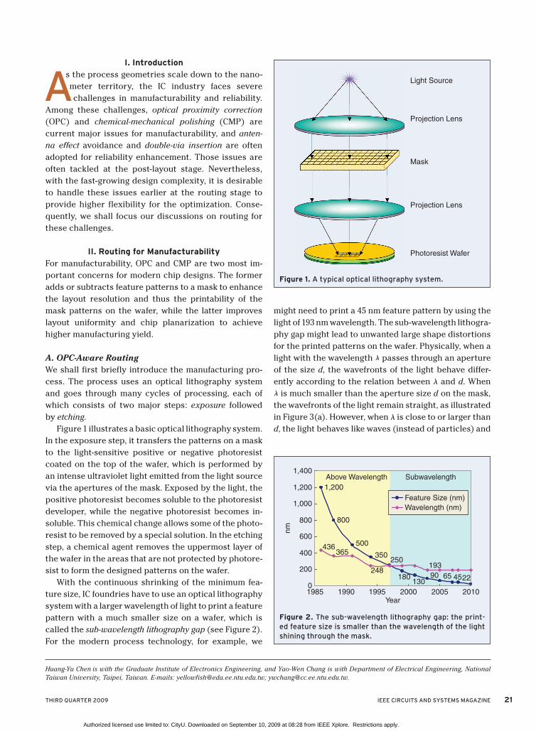
Figure 1 illustrates a basic optical lithography system.
In the exposure step, it transfers the patterns on a mask
to the light-sensitive positive or negative photoresist
coated on the top of the wafer, which is performed by
an intense ultraviolet light emitted from the light source
via the apertures of the mask. Exposed by the light, the
positive photoresist becomes soluble to the photoresist
developer, while the negative photoresist becomes in-
soluble. This chemical change allows some of the photo-
resist to be removed by a special solution. In the etching
step, a chemical agent removes the uppermost layer of
the wafer in the areas that are not protected by photore-
sist to form the designed patterns on the wafer.
With the continuous shrinking of the minimum fea-
ture size, IC foundries have to use an optical lithography
system with a larger wavelength of light to print a feature
pattern with a much smaller size on a wafer, which is
called the sub-wavelength lithography gap (see Figure 2).
For the modern process technology, for example, we
might need to print a 45 nm feature pattern by using the
light of 193 nm wavelength. The sub-wavelength lithogra-
phy gap might lead to unwanted large shape distortions
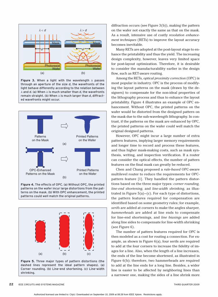
for the printed patterns on the wafer. Physically, when a
light with the wavelength l passes through an aperture
of the size d, the wavefronts of the light behave differ-
ently according to the relation between l and d. When
l is much smaller than the aperture size d on the mask,
the wavefronts of the light remain straight, as illustrated
in Figure 3(a). However, when l is close to or larger than
d, the light behaves like waves (instead of particles) and
A
Figure 1. A typical optical lithography system.
Light Source
Projection Lens
Projection Lens
Photoresist Wafer
Mask
Figure 2. The sub-wavelength lithography gap: the print-ed feature size is smaller than the wavelength of the light shining through the mask.
SubwavelengthAbove Wavelength
800
22456590
350
1,200
500
250
180130
365
248193
436
0
200
400
600
800
1,000
1,200
1,400
1985 1990 1995 2000 2005 2010Year
nm
Feature Size (nm)
Wavelength (nm)
Authorized licensed use limited to: CityU. Downloaded on September 10, 2009 at 08:28 from IEEE Xplore. Restrictions apply.
22 IEEE CIRCUITS AND SYSTEMS MAGAZINE THIRD QUARTER 2009
diffraction occurs (see Figure 3(b)), making the pattern
on the wafer not exactly the same as that on the mask.
As a result, intensive use of costly resolution enhance-
ment techniques (RETs) to improve the layout accuracy
becomes inevitable.
Many RETs are adopted at the post-layout stage to en-
hance the printability and thus the yield. The increasing
design complexity, however, leaves very limited space
for post-layout optimization. Therefore, it is desirable
to consider the manufacturability earlier in the design
flow, such as RET-aware routing.
Among the RETs, optical proximity correction (OPC) is
most popular in industry. OPC is the process of modify-
ing the layout patterns on the mask (drawn by the de-
signers) to compensate for the non-ideal properties of
the lithography process and thus to enhance the layout
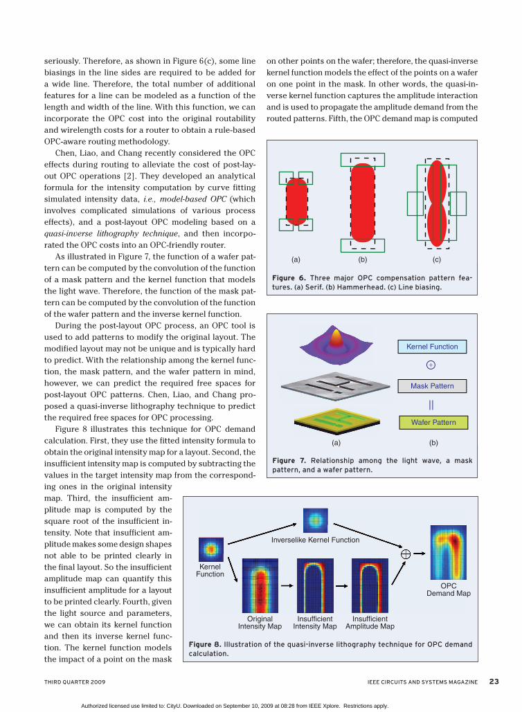
printability. Figure 4 illustrates an example of OPC en-
hancement. Without OPC, the printed patterns on the
wafer would be distorted from the designed pattern on
the mask due to the sub-wavelength lithography. In con-
trast, if the patterns on the mask are enhanced by OPC,
the printed patterns on the wafer could well match the
original designed patterns.
However, OPC might incur a large number of extra
pattern features, implying larger memory requirements
and longer time to record and process these features,
and thus higher mask-making costs, such as mask syn-
thesis, writing, and inspection verification. If a router
can consider the optical effects, the number of pattern
features on the final mask can greatly be reduced.
Chen and Chang proposed a rule-based OPC-aware
multilevel router to reduce the requirements for OPC-
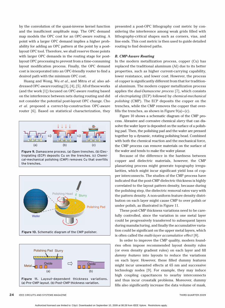
pattern feature [1]. They handled the pattern distor-
tions based on the three major types: corner rounding,
line-end shortening, and line-width shrinking, as illus-
trated in Figure 5(a)–(c). For each type of distortions,
the pattern features required for compensation are
identified based on some geometry rules; for example,
serifs are added at corners to make the angles sharper,
hammerheads are added at line ends to compensate
for line-end shortenings, and line biasings are added
along line sides to compensate for line-width shrinking
(see Figure 6).
The number of pattern features required for OPC is
then modeled as a cost for routing a connection. For ex-
ample, as shown in Figure 6(a), four serifs are required
to add at the four corners to increase the fidelity of im-
ages for a line. Also, when the length of a line increases,
the ends of the line become shortened, as illustrated in
Figure 6(b); therefore, two hammerheads are required
to add at the line ends for a long line. Besides, a wider
line is easier to be affected by neighboring lines than
a narrower one, making the sides of a line shrink more
Figure 3. When a light with the wavelength l passes through an aperture of the size d, the wavefronts of the light behave differently according to the relation between l and d. (a) When l is much smaller than d, the wavefronts remain straight. (b) When l is much larger than d, diffract-ed wavefronts might occur.
λ < d λ > d
Mask
PhotoresistWafer
PhotoresistWafer
Mask
d d
(a) (b)
Figure 4. The effects of OPC. (a) Without OPC, the printed patterns on the wafer incur large distortions from the pat-terns on the mask. (b) With OPC enhancement, the printed patterns could well match the original patterns.
Patterns
on the Mask
Printed Patterns
on the Wafer
OPC-Enhanced
Patterns on the Mask
(a)
(b)
Printed Patterns
on the Wafer
Figure 5. Three major types of pattern distortions (the dashed lines represent the ideal pattern shapes). (a) Corner rounding. (b) Line-end shortening. (c) Line-width shrinking.
(a) (b) (c)
Authorized licensed use limited to: CityU. Downloaded on September 10, 2009 at 08:28 from IEEE Xplore. Restrictions apply.
THIRD QUARTER 2009 IEEE CIRCUITS AND SYSTEMS MAGAZINE 23
seriously. Therefore, as shown in Figure 6(c), some line
biasings in the line sides are required to be added for
a wide line. Therefore, the total number of additional
features for a line can be modeled as a function of the
length and width of the line. With this function, we can
incorporate the OPC cost into the original routability
and wirelength costs for a router to obtain a rule-based
OPC-aware routing methodology.
Chen, Liao, and Chang recently considered the OPC
effects during routing to alleviate the cost of post-lay-
out OPC operations [2]. They developed an analytical
formula for the intensity computation by curve fitting
simulated intensity data, i.e., model-based OPC (which
involves complicated simulations of various process
effects), and a post-layout OPC modeling based on a
quasi-inverse lithography technique, and then incorpo-
rated the OPC costs into an OPC-friendly router.
As illustrated in Figure 7, the function of a wafer pat-
tern can be computed by the convolution of the function
of a mask pattern and the kernel function that models
the light wave. Therefore, the function of the mask pat-
tern can be computed by the convolution of the function
of the wafer pattern and the inverse kernel function.
During the post-layout OPC process, an OPC tool is
used to add patterns to modify the original layout. The
modified layout may not be unique and is typically hard
to predict. With the relationship among the kernel func-
tion, the mask pattern, and the wafer pattern in mind,
however, we can predict the required free spaces for
post-layout OPC patterns. Chen, Liao, and Chang pro-
posed a quasi-inverse lithography technique to predict
the required free spaces for OPC processing.
Figure 8 illustrates this technique for OPC demand
calculation. First, they use the fitted intensity formula to
obtain the original intensity map for a layout. Second, the
insufficient intensity map is computed by subtracting the
values in the target intensity map from the correspond-
ing ones in the original intensity
map. Third, the insufficient am-
plitude map is computed by the
square root of the insufficient in-
tensity. Note that insufficient am-
plitude makes some design shapes
not able to be printed clearly in
the final layout. So the insufficient
amplitude map can quantify this
insufficient amplitude for a layout
to be printed clearly. Fourth, given
the light source and parameters,
we can obtain its kernel function
and then its inverse kernel func-
tion. The kernel function models
the impact of a point on the mask
on other points on the wafer; therefore, the quasi-inverse
kernel function models the effect of the points on a wafer
on one point in the mask. In other words, the quasi-in-
verse kernel function captures the amplitude interaction
and is used to propagate the amplitude demand from the
routed patterns. Fifth, the OPC demand map is computed
Figure 6. Three major OPC compensation pattern fea-tures. (a) Serif. (b) Hammerhead. (c) Line biasing.
(a) (b) (c)
Figure 7. Relationship among the light wave, a mask pattern, and a wafer pattern.
Kernel Function
Mask Pattern
Wafer Pattern
+
(a) (b)
Figure 8. Illustration of the quasi-inverse lithography technique for OPC demand calculation.
KernelFunction
Inverselike Kernel Function
OriginalIntensity Map
InsufficientIntensity Map
InsufficientAmplitude Map
OPCDemand Map
Authorized licensed use limited to: CityU. Downloaded on September 10, 2009 at 08:28 from IEEE Xplore. Restrictions apply.
24 IEEE CIRCUITS AND SYSTEMS MAGAZINE THIRD QUARTER 2009
by the convolution of the quasi-inverse kernel function
and the insufficient amplitude map. The OPC demand
map models the OPC cost for an OPC-aware routing. A
point with a larger OPC demand implies a higher prob-
ability for adding an OPC pattern at the point by a post-
layout OPC tool. Therefore, we shall reserve those points
with larger OPC demands in the routing stage for post-
layout OPC processing to prevent from a time-consuming
layout modification process. Finally, the OPC demand
cost is incorporated into an OPC-friendly router to find a
desired path with the minimum OPC cost.
Huang and Wong, Wu et al., and Mitra et al. also ad-
dressed OPC-aware routing [3], [4], [5]. All of these works
(and the work [1]) focused on OPC-aware routing based
on the interference between nets during routing and did
not consider the potential post-layout OPC change. Cho
et al. proposed a correct-by-construction OPC-aware
router [6]. Based on statistical characterization, they
presented a post-OPC lithography cost metric by con-
sidering the interference among weak grids filled with
lithography-critical shapes such as corners, vias, and
line ends. This cost metric is then used to guide detailed
routing to find desired paths.
B. CMP-Aware RoutingIn the modern metallization process, copper (Cu) has
replaced the traditional aluminum (Al) due to its better
properties, such as higher current-carrying capability,
lower resistance, and lower cost. However, the process
of copper is significantly different from that for tradition-
al aluminum. The modern copper metallization process
applies the dual-Damascene process [7], which consists
of electroplating (ECP) followed by chemical-mechanical
polishing (CMP). The ECP deposits the copper on the
trenches, while the CMP removes the copper that over-
fills the trenches, as shown in Figure 9(a)–(c).
Figure 10 shows a schematic diagram of the CMP pro-
cess. Abrasive and corrosive chemical slurry that can dis-
solve the wafer layer is deposited on the surface of a polish-
ing pad. Then, the polishing pad and the wafer are pressed
together by a dynamic, rotating polishing head. Combined
with both the chemical reaction and the mechanical force,
the CMP process can remove materials on the surface of
the wafer and tends to make the wafer planar.
Because of the difference in the hardness between
copper and dielectric materials, however, the CMP
planarizing process might generate topography irregu-
larities, which might incur significant yield loss of cop-
per interconnects. The studies of the CMP process have
indicated that the post-CMP dielectric thickness is highly
correlated to the layout pattern density, because during
the polishing step, the dielectric removal rates vary with
the pattern density. A non-uniform feature density distri-
bution on each layer might cause CMP to over polish or
under polish, as illustrated in Figure 11.
These post-CMP thickness variations need to be care-
fully controlled, since the variation in one metal layer
could be progressively transferred to subsequent layers
during manufacturing, and finally the accumulative varia-
tion could be significant on the upper metal layers, which
is often called the multi-layer accumulative effect [8].
In order to improve the CMP quality, modern found-
ries often impose recommended layout density rules
(or even density gradient rules) on each layer and fill
dummy features into layouts to reduce the variations
on each layer. However, these filled dummy features
might incur unwanted effects at 65 nm and successive
technology nodes [9]. For example, they may induce
high coupling capacitances to nearby interconnects
and thus incur crosstalk problems. Moreover, dummy
fills also significantly increase the data volume of mask,
Figure 9. Damascene process. (a) Open trenches. (b) Elec-troplating (ECP) deposits Cu on the trenches. (c) Chemi-cal-mechanical polishing (CMP) removes Cu that overfills the trenches.
(a) (b) (c)
Figure 10. Schematic diagram of the CMP polisher.
Polishing HeadSlurry
Polishing Pad
Wafer
Figure 11. Layout-dependent thickness variations. (a) Pre-CMP layout. (b) Post-CMP thickness variation.
Oxide
Polishing Pad Slurry
OxideMetal
Oxide
(b)(a)
Authorized licensed use limited to: CityU. Downloaded on September 10, 2009 at 08:28 from IEEE Xplore. Restrictions apply.
THIRD QUARTER 2009 IEEE CIRCUITS AND SYSTEMS MAGAZINE 25
lengthening the time of mask-making processes and
thus the mask cost. Especially, these filled features
would significantly increase the input data in the follow-
ing time-consuming RETs, such as the OPC process.
Wire density greatly affects dummy feature filling. The
layout pattern (consisting of wires and dummy features)
density strongly depends on the wire density distribution,
as reported in [10]. Therefore, controlling wire density at
the routing stage can alleviate the problems induced by
aggressive dummy feature filling. Additionally, good wire
distribution can reduce the random particle short defects
and also benefit the post-layout redundant-via insertion
(see Section III-B), which can translate into yield gain.
The density uniformity in different routing stages for
CMP variation control has been addressed in the litera-
ture [10], [11], [12]. Cho et al. considered CMP variation
during global routing [10]. They empirically showed that
the number of inserted dummy features can be predicted
by the wire density and observed that a path with higher
pin density may not get much benefit from the wire density
optimization since there is little room for improvement (it
is destined to have high wire density from the beginning).
Therefore, they proposed a minimum pin-density global-
routing algorithm to reduce the maximum wire density.
Figure 12 illustrates the minimum pin-density global-
routing algorithm. A net from the source S to the tar-
get T to be routed is shown in Figure 12(a) with a pin
distribution. If only the L-shaped (1-bend) routing paths
are allowed, there are two possible paths, a and b, with
the same wirelength but different pin densities. Since the
existence of a pin implies at least one connection to other
pins, a path with higher pin density like b would tend to
have higher wire density eventually as shown in Figure
12(b), resulting in higher final wire densities. Therefore,
a path with the minimum pin density (like path a) leads
to better wire density distribution.
Chen et al. presented a full-chip two-pass, top-down
routing framework considering wire-distribution unifor-
mity for density variation minimization [11]. See Figure 13
for an illustration. To fully consider wire distribution,
Figure 12. Minimum pin-density global routing [10]. (a) There are two possible 1-bend paths a and b from the source S to the target T. (b) The path a with smaller pin density is better than the path b.
a aT T
S Sb b
(a) (b)
Figure 13. The new two-pass, top-down planarization-driven routing framework.
High
Low
G2
G1
G0
G2
G1
G0
To-be-Routed Net Already-Routed Net
Apply prerouting-guided
planarization-aware global
routing for local nets and
iteratively refine the
solution.
First-Pass Stage
Use segment-to-segment
detailed routing to route
short segments and reroute
failed nets level by level.
Second-Pass Stage
Identify the potential density
hot spots based on the pin
distribution and wire
connection to guide the
following global routing.
Prerouting Stage
Density Analysis
Uncoarsening
Uncoarsening
Uncoarsening
Uncoarsening
Layer/Track Assignment
Perform density-driven
layer/track assignment
for long segments panel
by panel.
Intermediate Stage
Authorized licensed use limited to: CityU. Downloaded on September 10, 2009 at 08:28 from IEEE Xplore. Restrictions apply.
26 IEEE CIRCUITS AND SYSTEMS MAGAZINE THIRD QUARTER 2009
the planarization-driven router consists of four major
stages: (1) Prerouting: Identify the potential density hot
spots based on the pin distribution and wire connection
to guide the following global routing, (2) Global rout-
ing: Apply prerouting-guided planarization-aware global
pattern routing for local nets and iteratively refine the
solution, (3) Layer/track assignment: Perform density-
driven layer/track assignment for long segments region
by region, and (4) Detailed routing: Use segment-to-
segment detailed maze routing to route short segments
and reroute failed nets level by level. By handling longer
nets first, the routing density for CMP can be better opti-
mized since the longer nets have higher density impact
than the shorter ones.
III. Routing for Reliability
Manufacturing reliability and yield in VLSI designs
are becoming a crucial challenge as the feature sizes
shrink into the nanometer scale. Both the antenna effect
arising in the plasma process and the via-open defect
are important issues for achieving a higher reliability
and yield.
A. Antenna-Avoidance RoutingThe antenna effect is caused by the charges collected
on the floating interconnects which are connected to
only a gate oxide. During the metallization, long float-
ing interconnects act as temporary capacitors and store
charges gained from the energy provided by fabrication
steps such as plasma etching and CMP. If the collected
charges exceed a threshold, the Fowler-Nordheim (F-N)
tunneling current will discharge through the thin oxide
and cause gate damage. On the other hand, if the col-
lected charges can be released before exceeding the
threshold through a low impedance path, such as diffu-
sion, the gate damage can be avoided.
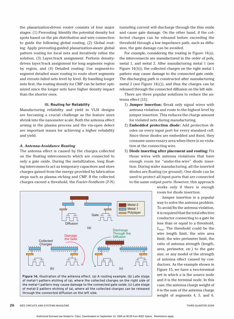
For example, considering the routing in Figure 14(a),
the interconnects are manufactured in the order of poly,
metal 1, and metal 2. After manufacturing metal 1 (see
Figure 14(b)), the collected charges on the right metal 1
pattern may cause damage to the connected gate oxide.
The discharging path is constructed after manufacturing
metal 2 (see Figure 14(c)), and thus the charges can be
released through the connected diffusion on the left side.
There are three popular solutions to reduce the an-
tenna effect [13]:
Jumper insertion:1) Break only signal wires with
antenna violation and route to the highest level by
jumper insertion. This reduces the charge amount
for violated nets during manufacturing.
Embedded protection diode:2) Add protection di-
odes on every input port for every standard cell.
Since these diodes are embedded and fi xed, they
consume unnecessary area when there is no viola-
tion at the connecting wire.
Diode inserting after placement and routing:3) Fix
those wires with antenna violations that have
enough room for “under-the-wire” diode inser-
tion. During wafer manufacturing, all the inserted
diodes are fl oating (or ground). One diode can be
used to protect all input ports that are connected
to the same output ports. However, this approach
works only if there is enough
room for diode insertion.
Jumper insertion is a popular
way to solve the antenna problem.
To avoid/fix the antenna violation,
it is required that the total effective
conductor connecting to a gate be
less than or equal to a threshold,
Lmax. The threshold could be the
wire length limit, the wire area
limit, the wire perimeter limit, the
ratio of antenna strength (length,
area, perimeter, etc.) to the gate
size, or any model of the strength
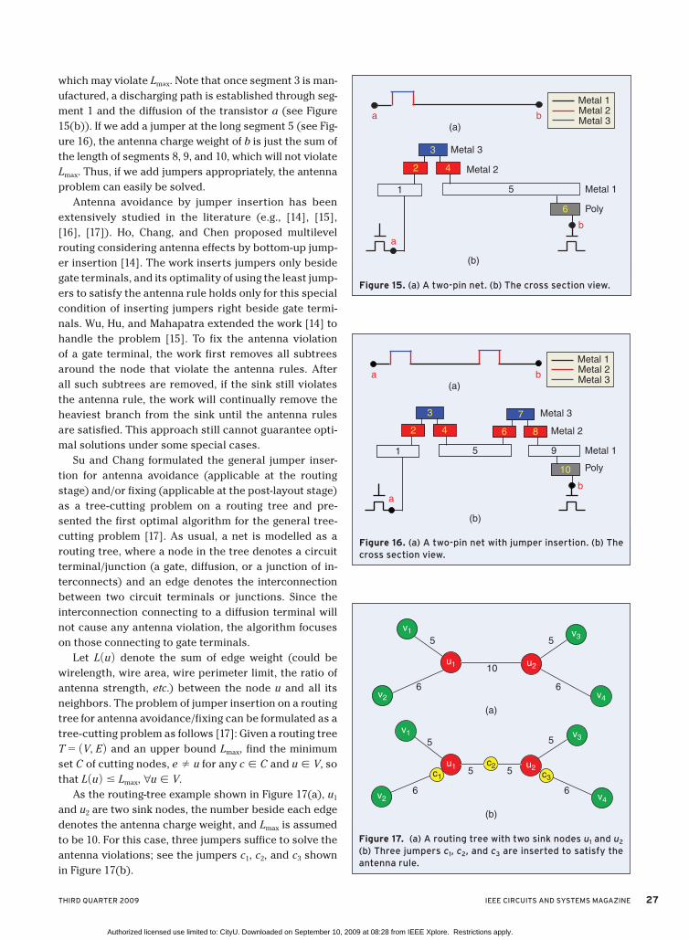
of antenna effect caused by con-
ductors. As the example shown in
Figure 15, we have a two-terminal
net in which a is the source node
and b is the terminal node. In this
case, the antenna charge weight of
b is the sum of the antenna charge
weight of segments 4, 5, and 6,
Figure 14. Illustration of the antenna effect. (a) A routing example. (b) Late stage of metal-1 pattern etching of (a), where the collected charges on the right side of the metal-1 pattern may cause damage to the connected gate oxide. (c) Late stage of metal-2 pattern etching of (a), where all the collected charges can be released through the connected diffusion on the left side.
Metal 2Metal 1Polylayer
Diffusion
Gate
(a)
(b) (c)
+ + + + + + + + + + + + + +
+ + + + + + + + + + + + + +
+ + + + + + +
+ + + + + + +
CollectedCharges
Damagethe Gate
+ + + + + + + + + + + + +
+ + + + + + + + + + + ++ + + + + + +
+ + + ++ + + + + + +
+ + + + + + + + + +
DischargeThrough theDiffusion
Authorized licensed use limited to: CityU. Downloaded on September 10, 2009 at 08:28 from IEEE Xplore. Restrictions apply.
THIRD QUARTER 2009 IEEE CIRCUITS AND SYSTEMS MAGAZINE 27
which may violate Lmax. Note that once segment 3 is man-
ufactured, a discharging path is established through seg-
ment 1 and the diffusion of the transistor a (see Figure
15(b)). If we add a jumper at the long segment 5 (see Fig-
ure 16), the antenna charge weight of b is just the sum of
the length of segments 8, 9, and 10, which will not violate
Lmax. Thus, if we add jumpers appropriately, the antenna
problem can easily be solved.
Antenna avoidance by jumper insertion has been
extensively studied in the literature (e.g., [14], [15],
[16], [17]). Ho, Chang, and Chen proposed multilevel
routing considering antenna effects by bottom-up jump-
er insertion [14]. The work inserts jumpers only beside
gate terminals, and its optimality of using the least jump-
ers to satisfy the antenna rule holds only for this special
condition of inserting jumpers right beside gate termi-
nals. Wu, Hu, and Mahapatra extended the work [14] to
handle the problem [15]. To fix the antenna violation
of a gate terminal, the work first removes all subtrees
around the node that violate the antenna rules. After
all such subtrees are removed, if the sink still violates
the antenna rule, the work will continually remove the
heaviest branch from the sink until the antenna rules
are satisfied. This approach still cannot guarantee opti-
mal solutions under some special cases.
Su and Chang formulated the general jumper inser-
tion for antenna avoidance (applicable at the routing
stage) and/or fixing (applicable at the post-layout stage)
as a tree-cutting problem on a routing tree and pre-
sented the first optimal algorithm for the general tree-
cutting problem [17]. As usual, a net is modelled as a
routing tree, where a node in the tree denotes a circuit
terminal/junction (a gate, diffusion, or a junction of in-
terconnects) and an edge denotes the interconnection
between two circuit terminals or junctions. Since the
interconnection connecting to a diffusion terminal will
not cause any antenna violation, the algorithm focuses
on those connecting to gate terminals.
Let L 1u 2 denote the sum of edge weight (could be
wirelength, wire area, wire perimeter limit, the ratio of
antenna strength, etc.) between the node u and all its
neighbors. The problem of jumper insertion on a routing
tree for antenna avoidance/fixing can be formulated as a
tree-cutting problem as follows [17]: Given a routing tree
T5 1V, E 2 and an upper bound Lmax, find the minimum
set C of cutting nodes, e 2 u for any c [ C and u [ V, so
that L 1u 2 # Lmax, 4u [ V.
As the routing-tree example shown in Figure 17(a), u1
and u2 are two sink nodes, the number beside each edge
denotes the antenna charge weight, and Lmax is assumed
to be 10. For this case, three jumpers suffice to solve the
antenna violations; see the jumpers c1, c2, and c3 shown
in Figure 17(b).
Figure 15. (a) A two-pin net. (b) The cross section view.
a
a
b
2
3
4
6
51
Metal 3
Metal 2
Metal 1
Poly
b
Metal 2Metal 3
Metal 1
(a)
(b)
Figure 16. (a) A two-pin net with jumper insertion. (b) The cross section view.
a
a
b
Metal 3
Metal 2
Metal 1
Poly
b
Metal 2Metal 3
Metal 1
(a)
(b)
1 5
2 4
3
10
6 8
7
9
Figure 17. (a) A routing tree with two sink nodes u1 and u2 (b) Three jumpers c1, c2, and c3 are inserted to satisfy the antenna rule.
c1
c2
c3
v1
v1
v3
v3
v4
v4
v2
v2
u1
u1
u2
u2
5
5
5
5
66
6 6
10
5 5
(a)
(b)
Authorized licensed use limited to: CityU. Downloaded on September 10, 2009 at 08:28 from IEEE Xplore. Restrictions apply.
28 IEEE CIRCUITS AND SYSTEMS MAGAZINE THIRD QUARTER 2009
Su and Chang showed that the aforementioned tree-cut-
ting problem exhibits the properties of optimal substruc-
tures and greedy choices. With these properties, a greedy
algorithm suffices to find an optimal solution [18]. Based
on the theory, they presented an O 1V 2 -time optimal jump-
er insertion algorithm that uses the minimum number of
jumpers to fix the antenna violations in a routing tree with
V vertices. The algorithm performs in a bottom-up manner
by dealing with leaf nodes first followed by sub-leaf nodes
of the tree. Here, a leaf node is a node with no children,
whereas a sub-leaf node is a node for which all its children
are leaf nodes, and if any of its children is a gate terminal,
the edges between it and its children all have weights Lmax.
For a leaf node which denotes a gate terminal (i.e., no
discharging path through this terminal), the edge con-
necting to this leaf node, with its weight exceeding Lmax,
a cutting node is assigned at the position that make the
edge weight equal to Lmax; otherwise, no cutting node
needs to be inserted.
For a sub-leaf node, if the total weight of the edges
between this node and its children is less than Lmax, the
total weight is added to this node and the processing
continues upward in the tree. On the other hand, if the
total weight is greater than Lmax, the edge weights be-
tween this node and its children are sorted into a non-
decreasing order, and a cutting node is added into each
edge with its partial sum (accumulated from the first
edge) greater than Lmax.
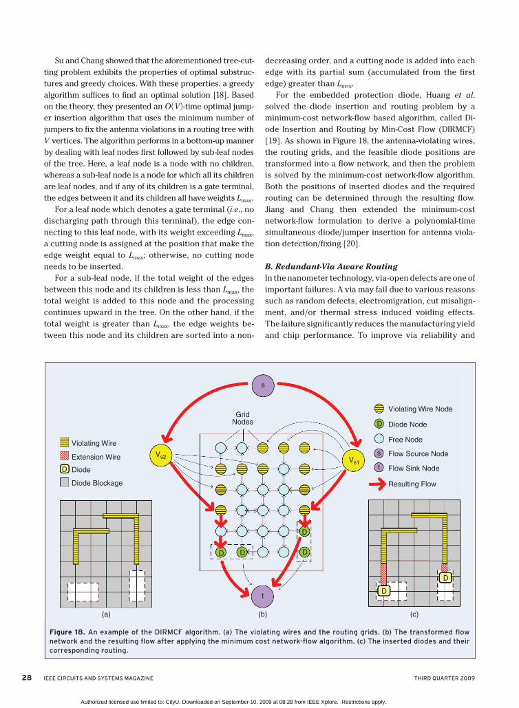
For the embedded protection diode, Huang et al.
solved the diode insertion and routing problem by a
minimum-cost network-flow based algorithm, called Di-
ode Insertion and Routing by Min-Cost Flow (DIRMCF)
[19]. As shown in Figure 18, the antenna-violating wires,
the routing grids, and the feasible diode positions are
transformed into a flow network, and then the problem
is solved by the minimum-cost network-flow algorithm.
Both the positions of inserted diodes and the required
routing can be determined through the resulting flow.
Jiang and Chang then extended the minimum-cost
network-flow formulation to derive a polynomial-time
simultaneous diode/jumper insertion for antenna viola-
tion detection/fixing [20].
B. Redundant-Via Aware RoutingIn the nanometer technology, via-open defects are one of
important failures. A via may fail due to various reasons
such as random defects, electromigration, cut misalign-
ment, and/or thermal stress induced voiding effects.
The failure significantly reduces the manufacturing yield
and chip performance. To improve via reliability and
Figure 18. An example of the DIRMCF algorithm. (a) The violating wires and the routing grids. (b) The transformed flow network and the resulting flow after applying the minimum cost network-flow algorithm. (c) The inserted diodes and their corresponding routing.
D
Violating Wire
Extension Wire
Diode
Diode Blockage
Violating Wire Node
Diode Node
Free Node
Flow Source Node
Flow Sink Node
Resulting Flow
D
s
s
GridNodes
Vs2Vs1
t
D
DDD
tD
D
(a) (b) (c)
Authorized licensed use limited to: CityU. Downloaded on September 10, 2009 at 08:28 from IEEE Xplore. Restrictions apply.
THIRD QUARTER 2009 IEEE CIRCUITS AND SYSTEMS MAGAZINE 29
yield, redundant-via insertion is a highly recommended
technique proposed by foundries. If a via fails, a redun-
dant via can serve as a fault-tolerant substitute for the
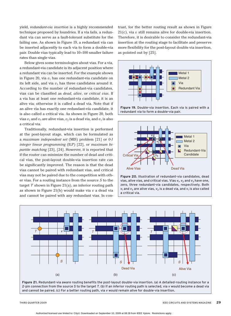
failing one. As shown in Figure 19, a redundant via can
be inserted adjacently to each via to form a double-via
pair. Double vias typically lead to 10–100 smaller failure
rates than single vias.
Below gives some terminologies about vias. For a via,
a redundant-via candidate is its adjacent position where
a redundant via can be inserted. For the example shown
in Figure 20, via v1 has one redundant-via candidate on
its left side, and via v3 has three candidates around it.
According to the number of redundant-via candidates,
vias can be classified as dead, alive, or critical vias. If
a via has at least one redundant-via candidate, it is an
alive via; otherwise it is called a dead via. Note that if
an alive via has exactly one redundant-via candidate, it
is also called a critical via. As shown in Figure 20, both
vias v1 and v3 are alive vias, v2 is a dead via, and v1 is also
a critical via.
Traditionally, redundant-via insertion is performed
at the post-layout stage, which can be formulated as
a maximum independent set (MIS) problem [21] or 0-1
integer linear programming (ILP) [22], or maximum bi-
partite matching [23], [24]. However, it is reported that
if the router can minimize the number of dead and criti-
cal vias, the post-layout double-via insertion rate can
be significantly improved. The reason is that the dead
vias cannot be paired with redundant vias, and critical
vias may not be paired due to the competition with oth-
er vias. For a routing instance from the source S to the
target T shown in Figure 21(a), an inferior routing path
as shown in Figure 21(b) would make via v a dead via
and cannot be paired with any redundant vias. In con-
trast, for the better routing result as shown in Figure
21(c), via v still remains alive for double-via insertion.
Therefore, it is desirable to consider the redundant-via
insertion at the routing stage to facilitate and preserve
more flexibility for the post-layout double via insertion,
as pointed out by [25].
Figure 19. Double-via insertion. Each via is paired with a redundant via to form a double-via pair.
Metal 1
Metal 2
Via
Redundant Via
Figure 20. Illustration of redundant-via candidates, dead vias, alive vias, and critical vias. Vias v1, v2 and v3 have one, zero, three redundant-via candidates, respectively. Both v1 and v3 are alive vias, v2 is a dead via, and v1 is also called a critical via.
Critical Via
Dead ViaAlive Vias
Metal 1
Metal 2
Via
Redundant-Via
Candidate
v1
v2
v3
Figure 21. Redundant-via aware routing benefits the post-layout double-via insertion. (a) A detailed-routing instance for a 2-pin connection from the source S to the target T. (b) If an inferior routing path is selected, via v would become a dead via and cannot be paired. (c) For a better routing path, via v would remain alive for double-via insertion.
S
T
S
T
S
T
Dead Via Alive Via
v
(a) (b) (c)
Authorized licensed use limited to: CityU. Downloaded on September 10, 2009 at 08:28 from IEEE Xplore. Restrictions apply.
30 IEEE CIRCUITS AND SYSTEMS MAGAZINE THIRD QUARTER 2009
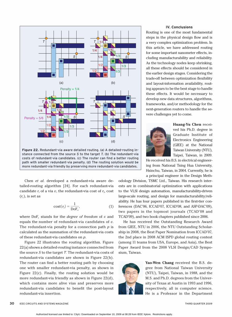
Chen et al. developed a redundant-via aware de-
tailed-routing algorithm [24]. For each redundant-via
candidate ri of a via v, the redundant-via cost of ri, cost
(ri ), is set as
cost 1ri 2 51
DoFv
, (1)
where DoFv stands for the degree of freedom of v and
equals the number of redundant-via candidates of v.
The redundant-via penalty for a connection path p is
calculated as the summation of the redundant-via costs
of these redundant-via candidates on p.
Figure 22 illustrates the routing algorithm. Figure
22(a) shows a detailed-routing instance connected from
the source S to the target T. The redundant-via costs of
redundant-via candidates are shown in Figure 22(b).
The router can find a better routing path by choosing
one with smaller redundant-via penalty, as shown in
Figure 22(c). Finally, the routing solution would be
more redundant-via friendly as shown in Figure 22(d),
which contains more alive vias and preserves more
redundant-via candidates to benefit the post-layout
redundant-via insertion.
IV. Conclusions
Routing is one of the most fundamental
steps in the physical design flow and is
a very complex optimization problem. In
this article, we have addressed routing
for some important nanometer effects, in-
cluding manufacturability and reliability.
As the technology nodes keep shrinking,
all these effects should be considered in
the earlier design stages. Considering the
trade-off between optimization flexibility
and layout-information availability, rout-
ing appears to be the best stage to handle
these effects. It would be necessary to
develop new data structures, algorithms,
frameworks, and/or methodology for the
next-generation routers to handle the se-
vere challenges yet to come.
Huang-Yu Chen recei-
ved his Ph.D. degree in
Graduate Institute of
Electronics Engineering
(GIEE) at the National
Taiwan University (NTU),
Taipei, Taiwan, in 2009.
He received his B.S. in electrical engineer-
ing from National Tsing Hua University,
Hsinchu, Taiwan, in 2004. Currently, he is
a principal engineer in the Design Meth-
odology Division, TSMC Ltd., Taiwan. His research inter-
ests are in combinatorial optimization with applications
to the VLSI design automation, manufacturability-driven
large-scale routing, and design for manufacturability/reli-
ability. He has four papers published in the first-tier con-
ferences (DAC’06, ICCAD’07, ICCAD’08, and ASP-DAC’09),
two papers in the topmost journals (TCAD’08 and
TCAD’09), and two book chapters published since 2006.
He has received the Outstanding Research Award
from GIEE, NTU in 2006, the NTU Outstanding Scholar-
ship in 2008, the Best Paper Nomination from ICCAD’07,
the 2nd place in 2008 ACM ISPD global routing contest
(among 11 teams from USA, Europe, and Asia), the Best
Paper Award from the 2008 VLSI Design/CAD Sympo-
sium, Taiwan.
Yao-Wen Chang received the B.S. de-
gree from National Taiwan University
(NTU), Taipei, Taiwan, in 1988, and the
M.S. and Ph.D. degrees from the Univer-
sity of Texas at Austin in 1993 and 1996,
respectively, all in computer science.
He is a Professor in the Department
Figure 22. Redundant-via aware detailed routing. (a) A detailed-routing in-stance connected from the source S to the target T. (b) The redundant-via costs of redundant-via candidates. (c) The router can find a better routing path with smaller redundant-via penalty. (d) The routing solution would be more redundant-via friendly by preserving more redundant-via candidates.
S
T
S
T
1/3
1/3
1/3
1/4
1/4
1/4
1/4
1/2
S
T
Penalty = 5/6
Penalty = 1/4
1/3
1/3
1/3
1/4
1/4
1/4
1/4
1/2
1/2
S
T
1/2
(a) (b)
(c) (d)
Authorized licensed use limited to: CityU. Downloaded on September 10, 2009 at 08:28 from IEEE Xplore. Restrictions apply.
THIRD QUARTER 2009 IEEE CIRCUITS AND SYSTEMS MAGAZINE 31
of Electrical Engineering and the Graduate Institute of
Electronics Engineering, NTU. He is currently also a
Visiting Professor at Waseda University, Kitakyushu,
Japan. He was with National Chiao Tung University
(NCTU), Hsinchu, Taiwan from 1996 to 2001 and IBM
T.J. Watson Research Center in the summer of 1994.
His current research interests lie in VLSI physical de-
sign, design for manufacturability/reliability, and de-
sign automation for biochips. He has been working
closely with industry in these areas. He has co-edited
one textbook on EDA and coauthored one book on
routing and over 150 ACM/IEEE conference/journal pa-
pers in these areas.
Dr. Chang was a winner of the 2008 ACM ISPD Glob-
al Routing Contest and the 2006 ACM ISPD Placement
Contest. He was a recipient of Best Paper Awards at
IEEE ICCD-95 and the 2007 and 2008 VLSI Design/CAD
Symposia, and 12 Best Paper Award Nominations from
DAC (four times), ICCAD (twice), ISPD (three times),
ACM TODAES, ASP-DAC, and ICCD in the past eight
years. He has received many research awards, such as
the 2007 Outstanding Research Award, the inaugural
2005 First-Class Principal Investigator Award, and the
2004 Dr. Wu Ta You Memorial Award, all from National
Science Council of Taiwan, and the 2004 MXIC Young
Chair Professorship from the MXIC Corp, and excellent
teaching awards from NTU (four times) and NCTU.
He is currently an associate editor of IEEE Transac-
tions on Computer-Aided Design of Integrated Circuits
and Systems (TCAD) and an editor of the Journal of
Information Science and Engineering (JISE) and the
Journal of Electrical and Computer Engineering (JECE).
He has served on the ICCAD Executive Committee, the
ASP-DAC Steering Committee, the ACM/SIGDA Physical
Design Technical Committee, the ACM ISPD and IEEE
FPT Organizing Committees, and the technical pro-
gram committees of ASP-DAC, DAC, DATE, FPL, FPT,
GLSVLSI, ICCAD, ICCD, IECON, ISPD, SOCC, TENCON,
and VLSI-DAT. He is currently an independent board
director of Genesys Logic, Inc, a technical consultant
of RealTek Semiconductor Corp., a member of board
of governors of Taiwan IC Design Society, and a mem-
ber of the IEEE Circuits and Systems Society, ACM, and
ACM/SIGDA.
References[1] T.-C. Chen and Y.-W. Chang, “Multilevel full-chip gridless routing
with applications to optical proximity correction,” IEEE Trans. Comput-
er-Aided Design, vol. 26, no. 6, pp. 1041–1053, June 2007.
[2] T.-C. Chen, G.-W. Liao, and Y.-W. Chang, “Predictive formulae for OPC
with applications to lithography-friendly routing,” in Proc. ACM/IEEE
Design Automation Conf., Anaheim, CA, June 2008, pp. 510–515.
[3] L.-D. Huang and M. D. F. Wong, “Optical proximity correction (OPC)-
friendly maze routing,” in Proc. ACM/IEEE Design Automation Conf., San
Diego, CA, June 2004, pp. 186–191.
[4] Y.-R. Wu, M.-C. Tsai, and T.-C. Wang, “Maze routing with OPC con-
sideration,” in Proc. ACM/IEEE Asia and South Pacific Design Automation
Conf., Shanghai, China, Jan. 2005, pp. 198–203.
[5] J. Mitra, P. Yu, and D. Z. Pan, “RADAR: RET-aware detailed routing
using fast lithography simulations,” in Proc. ACM/IEEE Design Automa-
tion Conf., Anaheim, CA, June 2005, pp. 369–372.
[6] M. Cho, K. Yuan, Y. Ban, and D. Z. Pan, “ELIAD: Effi cient lithogra-
phy aware detailed router with compact printability prediction,” in
Proc. ACM/IEEE Design Automation Conf., Anaheim, CA, June 2008,
pp. 504–509.
[7] J. Luo, Q. Su, C. Chiang, and J. Kawa, “A layout dependent full-chip
copper electroplating topography model,” in Proc. IEEE/ACM Int. Conf.
Computer-Aided Design, San Jose, CA, Nov. 2005, pp. 133–140.
[8] R. Tian, D. F. Wong, and R. Boone, “Model-based dummy feature
placement for oxide chemical-mechanical polishing manufacturabil-
ity,” in Proc. ACM/IEEE Design Automation Conf., Anaheim, CA, June
2000, pp. 667–670.
[9] D. White and B. Moore, “An ‘intelligent’ approach to dummy fi ll,” EE
Times, Jan. 3, 2005.
[10] M. Cho, D. Z. Pan, H. Xiang, and R. Puri, “Wire density driven global
routing for CMP variation and timing,” in Proc. IEEE/ACM Int. Conf. Com-
puter-Aided Design, San Jose, CA, Nov. 2006, pp. 487–492.
[11] H.-Y. Chen, S.-J. Chou, S.-L. Wang, and Y.-W. Chang, “A novel wire
density driven full-chip routing system for CMP variation control,” IEEE
Trans. Computer-Aided Design, vol. 28, no. 2, pp. 193–206, Feb. 2009.
[12] K. S.-M. Li, C.-L. Lee, Y.-W. Chang, C.-C. Su, and J. E. Chen, “Multilev-
el full-chip routing with testability and yield enhancement,” IEEE Trans.
Computer-Aided Design, vol. 26, no. 9, pp. 1625–1636, Sept. 2007.
[13] P. H. Chen, S. Malkani, C.-M. Peng, and J. Lin, “Fixing antenna
problem by dynamic diode dropping and jumper insertion,” in Proc.
IEEE Int. Symp. Quality Electronic Design, Berkeley, CA, Mar. 2000,
pp. 275–282.
[14] T.-Y. Ho, Y.-W. Chang, and S.-J. Chen, “Multilevel routing with an-
tenna avoidance,” in Proc. ACM Int. Symp. Physical Design, Phoenix, AZ,
Apr. 2004, pp. 34–40.
[15] D. Wu, J. Hu, and R. Mahapatra, “Coupling aware timing optimi-
zation and antenna avoidance in layer assignment,” in Proc. ACM Int.
Symp. Physical Design, San Francisco, CA, Apr. 2005, pp. 20–27.
[16] T.-Y. Ho, Y.-W. Chang, and S.-J. Chen, Full-Chip Nanometer Routing
Techniques. Dordrecht, The Netherlands: Springer-Verlag, 2007.
[17] B.-Y. Su, Y.-W. Chang, and J. Hu, “An optimal jumper insertion al-
gorithm for antenna avoidance/fi xing,” IEEE Trans. Computer-Aided De-
sign, vol. 26, no. 10, pp. 1818–1929, Oct. 2007.
[18] T. H. Cormen, C. E. Leiserson, R. L. Rivest, and C. Stein, Introduction
to Algorithms, 2nd ed. New York: McGraw-Hill, 2001.
[19] L.-D. Huang, X. Tang, H. Xiang, D. F. Wong, and I.-M. Liu, “A polyno-
mial time optimal diode insertion/routing algorithm for fi xing antenna
problem,” IEEE Trans. Computer-Aided Design, vol. 23, no. 1, pp. 141–147,
Jan. 2004.
[20] Z.-W. Jiang and Y.-W. Chang, “An optimal network-fl ow-based simul-
taneous diode and jumper insertion algorithm for antenna fi xing,” IEEE
Trans. Computer-Aided Design, vol. 27, no. 6, pp. 1055–1065, June 2008.
[21] K.-Y. Lee and T.-C. Wang, “Post-routing redundant via insertion for
yield/reliability improvement,” in Proc. ACM/IEEE Asia and South Pacific
Design Automation Conf., Yokohama, Japan, Jan. 2006, pp. 303–308.
[22] K.-Y. Lee, C.-K. Koh, T.-C. Wang, and K.-Y. Chao, “Optimal post-rout-
ing redundant via insertion,” in Proc. ACM Int. Symp. Physical Design,
Portland, OR, Apr. 2008, pp. 111–117.
[23] H. Yao, Y. Cai, X. Hong, and Q. Zhou, “Improved multilevel routing
with redundant via placement for yield and reliability,” in Proc. ACM
Great Lakes Symp. VLSI, Chicago, IL, Apr. 2005, pp. 143–146.
[24] H.-Y. Chen, M.-F. Chiang, Y.-W. Chang, L. Chen, and B. Han, “Full-
chip routing considering double-via insertion,” IEEE Trans. Computer-
Aided Design, vol. 27, no. 5, pp. 844–857, May 2008.
[25] G. Xu, L.-D. Huang, D. Z. Pan, and M. D. Wong, “Redundant-via en-
hanced maze routing for yield improvement,” in Proc. ACM/IEEE Asia
and South Pacific Design Automation Conf., Shanghai, China, Jan. 2005,
pp. 1148–1151.
Authorized licensed use limited to: CityU. Downloaded on September 10, 2009 at 08:28 from IEEE Xplore. Restrictions apply.