Embed Size (px)
Citation preview
HAL Id: lirmm-00803451https://hal-lirmm.ccsd.cnrs.fr/lirmm-00803451
Submitted on 21 Jan 2017
HAL is a multi-disciplinary open accessarchive for the deposit and dissemination of sci-entific research documents, whether they are pub-lished or not. The documents may come fromteaching and research institutions in France orabroad, or from public or private research centers.
L’archive ouverte pluridisciplinaire HAL, estdestinée au dépôt et à la diffusion de documentsscientifiques de niveau recherche, publiés ou non,émanant des établissements d’enseignement et derecherche français ou étrangers, des laboratoirespublics ou privés.
Design-for-manufacturability of MEMS convectiveaccelerometers through adaptive electrical calibration
strategyAhmed Rekik, Florence Azaïs, Frédérick Mailly, Pascal Nouet
To cite this version:Ahmed Rekik, Florence Azaïs, Frédérick Mailly, Pascal Nouet. Design-for-manufacturability of MEMSconvective accelerometers through adaptive electrical calibration strategy. LATW: Latin AmericanTest Workshop, Apr 2012, Quito, Ecuador. �10.1109/LATW.2012.6261237�. �lirmm-00803451�
Design-for-manufacturability of MEMS convective accelerometers through adaptive
electrical calibration strategy A.A. Rekik1,2, F. Azaïs1, F. Mailly1, P. Nouet1
1 LIRMM - CNRS/Univ. Montpellier 2 - 161 rue Ada, 34392 Montpellier, France 2 ENIS - University of Sfax - Route Soukra, Cité Elhabib BP W 3052 Sfax, Tunisia
Abstract— In this paper, we explore the use of an adaptive electrical calibration strategy in the context of design-for-manufacturing for MEMS convective accelerometers. The calibration principle relies on the adjustment of the heater power level such that sensitivity is set to a given target value. The idea is to define multiple sensitivity targets in order to improve production yield and to insert a criterion on power consumption. Different device binning can then be achieved depending on test limit settings. Results obtained from Monte-Carlo simulation are presented to demonstrate potentialities of the technique.
Keywords— MEMS, convective accelerometer, test, calibration, design-for-manufacturing
I. INTRODUCTION
MEMS convective accelerometers are an interesting alternative to comb-drive accelerometers even if current market is largely devoted to the latter [1]. Their interest is twofold. On the one side, they can be fabricated in a CMOS technology with a single self-aligned additional etching [2]. This post-process called Front-Side Bulk Micromachining is one of the most popular in MEMS. On the other side, such accelerometers exhibit large dynamic range and huge safety range (they can support several thousands of g’s without any damage).
Apart from the previous two advantages, we intend to demonstrate in this paper that convective accelerometers can be associated with design for manufacturing approaches to make them more appealing. Design for Manufacturability (DfM) generally includes Design for Test, Calibration, Reliability… often called DfX [3]. In our case, convective accelerometers already demonstrated their reliability so it is not necessary to work on their design to improve reliability. In some previous studies, we proposed techniques for test and calibration of such accelerometers using electrical-only stimuli [4-6]. This point is really important as the cost of these test procedures may drastically impact the final cost in the case of low-end products such as those used for consumer applications. In this paper, we propose to extend the previously proposed go/no-go scheme to a complete calibration and binning procedure.
The paper is organized as follow. In section II, the Device Under Test (DUT) is introduced together with a parametric fault model used to represent process scattering effects. In section III, electrical-only calibration procedure is described to introduce, in section IV, the adaptive electrical calibration strategy that allows binning on device sensitivity and power consumption. Finally, section V reports experimental results before conclusion.
II. DEVICE UNDER TEST OVERVIEW
A. Device description
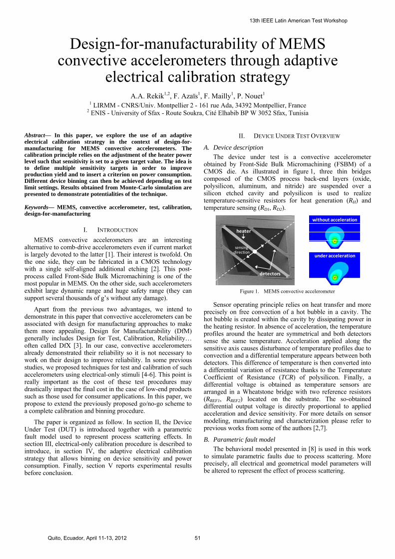
The device under test is a convective accelerometer obtained by Front-Side Bulk Micromachining (FSBM) of a CMOS die. As illustrated in figure 1, three thin bridges composed of the CMOS process back-end layers (oxide, polysilicon, aluminum, and nitride) are suspended over a silicon etched cavity and polysilicon is used to realize temperature-sensitive resistors for heat generation (RH) and temperature sensing (RD1, RD2).
Figure 1. MEMS convective accelerometer
Sensor operating principle relies on heat transfer and more precisely on free convection of a hot bubble in a cavity. The hot bubble is created within the cavity by dissipating power in the heating resistor. In absence of acceleration, the temperature profiles around the heater are symmetrical and both detectors sense the same temperature. Acceleration applied along the sensitive axis causes disturbance of temperature profiles due to convection and a differential temperature appears between both detectors. This difference of temperature is then converted into a differential variation of resistance thanks to the Temperature Coefficient of Resistance (TCR) of polysilicon. Finally, a differential voltage is obtained as temperature sensors are arranged in a Wheatstone bridge with two reference resistors (RREF1, RREF2) located on the substrate. The so-obtained differential output voltage is directly proportional to applied acceleration and device sensitivity. For more details on sensor modeling, manufacturing and characterization please refer to previous works from some of the authors [2,7].
B. Parametric fault model
The behavioral model presented in [8] is used in this work to simulate parametric faults due to process scattering. More precisely, all electrical and geometrical model parameters will be altered to represent the effect of process scattering.
heater
detectors
sensing direction
without acceleration
under acceleration
13th IEEE Latin American Test Workshop
Quito, Ecuador, April 11-13, 2012 51
In particular, we consider a Gaussian distribution with 3=20% for electrical resistances, i.e. heater resistance RH0, detectors’ resistances RDi0, and reference resistances RREFi. This distribution corresponds to typical uncertainties given by the foundry and is a global variation, i.e. it affects all resistances in the same amount. In addition, we consider a mismatch error with 3=2% for detectors’ resistances RDi0 and reference resistances RREFi. We also consider a Gaussian distribution with 3=10% for polysilicon temperature coefficient of resistance TCR as this parameter is quite sensitive to doping fluctuations.
Regarding geometrical parameters, we consider a Gaussian distribution with 3=2µm for the distance r2 between the heater and the cavity boundary. Indeed, lateral dimensions are parameters that are rather well controlled during the manufacturing process and exhibit a low dispersion. In contrast, the cavity depth h1 is a parameter that it is very sensitive to the etching post-process (etching solution composition, etching time and etching solution movements) and therefore very difficult to control. As we have no information from the foundry, we consider a random uniform variation of cavity depth h1 between 50µm and 490µm.
III. PREVIOUS WORK ON ELECTRICAL CALIBRATION
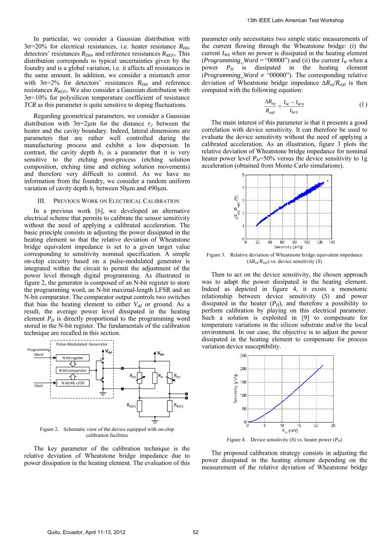
In a previous work [6], we developed an alternative electrical scheme that permits to calibrate the sensor sensitivity without the need of applying a calibrated acceleration. The basic principle consists in adjusting the power dissipated in the heating element so that the relative deviation of Wheatstone bridge equivalent impedance is set to a given target value corresponding to sensitivity nominal specification. A simple on-chip circuitry based on a pulse-modulated generator is integrated within the circuit to permit the adjustment of the power level through digital programming. As illustrated in figure 2, the generator is composed of an N-bit register to store the programming word, an N-bit maximal-length LFSR and an N-bit comparator. The comparator output controls two switches that bias the heating element to either Vdd or ground. As a result, the average power level dissipated in the heating element PH is directly proportional to the programming word stored in the N-bit register. The fundamentals of the calibration technique are recalled in this section.
Figure 2. Schematic view of the device equipped with on-chip
calibration facilities
The key parameter of the calibration technique is the relative deviation of Wheatstone bridge impedance due to power dissipation in the heating element. The evaluation of this
parameter only necessitates two simple static measurements of the current flowing through the Wheatstone bridge: (i) the current IW0 when no power is dissipated in the heating element (Programming_Word = “00000”) and (ii) the current IW when a power PH is dissipated in the heating element (Programming_Word “00000”). The corresponding relative deviation of Wheatstone bridge impedance Req/Req0 is then computed with the following equation:
0
0
W
WW
eq0
eq
I
II
R
R
The main interest of this parameter is that it presents a good correlation with device sensitivity. It can therefore be used to evaluate the device sensitivity without the need of applying a calibrated acceleration. As an illustration, figure 3 plots the relative deviation of Wheatstone bridge impedance for nominal heater power level PH=50% versus the device sensitivity to 1g acceleration (obtained from Monte-Carlo simulations).
Figure 3. Relative deviation of Wheatstone bridge equivalent impedance
(Req/Req0) vs. device sensitivity (S)
Then to act on the device sensitivity, the chosen approach was to adapt the power dissipated in the heating element. Indeed as depicted in figure 4, it exists a monotonic relationship between device sensitivity (S) and power dissipated in the heater (PH), and therefore a possibility to perform calibration by playing on this electrical parameter. Such a solution is exploited in [9] to compensate for temperature variations in the silicon substrate and/or the local environment. In our case, the objective is to adjust the power dissipated in the heating element to compensate for process variation device susceptibility.
Figure 4. Device sensitivity (S) vs. heater power (PH)
The proposed calibration strategy consists in adjusting the power dissipated in the heating element depending on the measurement of the relative deviation of Wheatstone bridge
RD1 RD2RH
RREF1 RREF2
VddN‐bit register
N‐bit ML‐LFSR
Programming Word
Clock
N‐bit comparator
Vdd
Pulse‐Modulated Generator
13th IEEE Latin American Test Workshop
Quito, Ecuador, April 11-13, 2012 52
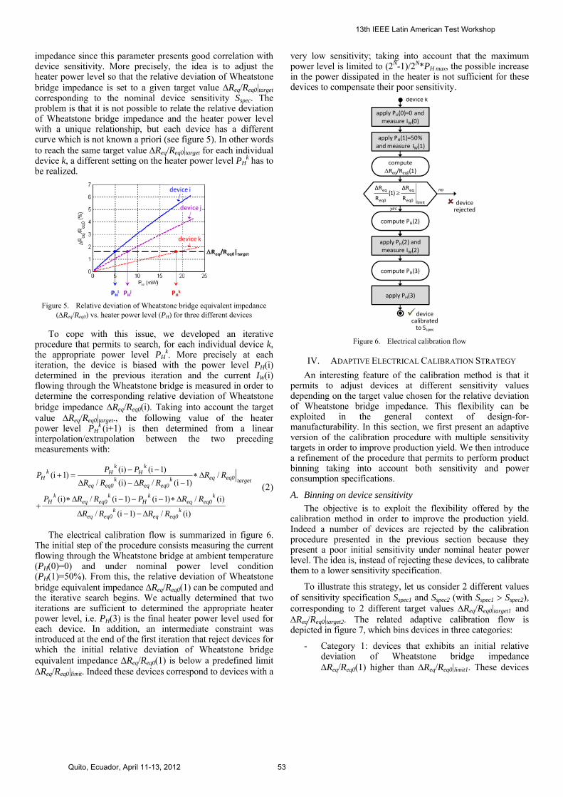
impedance since this parameter presents good correlation with device sensitivity. More precisely, the idea is to adjust the heater power level so that the relative deviation of Wheatstone bridge impedance is set to a given target value Req/Req0|target corresponding to the nominal device sensitivity Sspec. The problem is that it is not possible to relate the relative deviation of Wheatstone bridge impedance and the heater power level with a unique relationship, but each device has a different curve which is not known a priori (see figure 5). In other words to reach the same target value Req/Req0|target for each individual device k, a different setting on the heater power level PH
k has to be realized.
Figure 5. Relative deviation of Wheatstone bridge equivalent impedance
(Req/Req0) vs. heater power level (PH) for three different devices
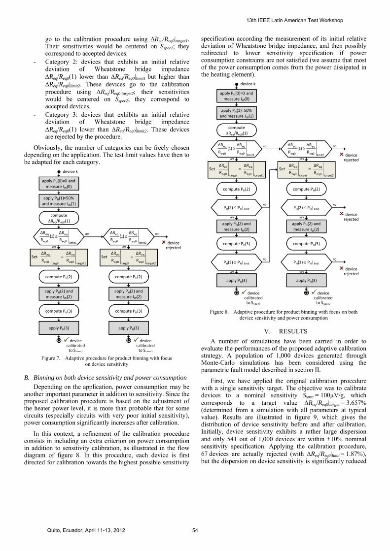
To cope with this issue, we developed an iterative procedure that permits to search, for each individual device k, the appropriate power level PH
k. More precisely at each iteration, the device is biased with the power level PH(i) determined in the previous iteration and the current IW(i) flowing through the Wheatstone bridge is measured in order to determine the corresponding relative deviation of Wheatstone bridge impedance Req/Req0(i). Taking into account the target value Req/Req0|target., the following value of the heater power level PH
k (i+1) is then determined from a linear interpolation/extrapolation between the two preceding measurements with:
)i(/)1i(/
)i(/)1i()1i(/)i(
/)1i(/)i(/
)1i()i()1i(
keq0eq
keq0eq
keq0eq
kH
keq0eq
kH
targeteq0eqkeq0eq
keq0eq
kH
kHk
H
RRRR
RRPRRP
RRRRRR
PPP
The electrical calibration flow is summarized in figure 6. The initial step of the procedure consists measuring the current flowing through the Wheatstone bridge at ambient temperature (PH(0)=0) and under nominal power level condition (PH(1)=50%). From this, the relative deviation of Wheatstone bridge equivalent impedance Req/Req0(1) can be computed and the iterative search begins. We actually determined that two iterations are sufficient to determined the appropriate heater power level, i.e. PH(3) is the final heater power level used for each device. In addition, an intermediate constraint was introduced at the end of the first iteration that reject devices for which the initial relative deviation of Wheatstone bridge equivalent impedance Req/Req0(1) is below a predefined limit Req/Req0|limit. Indeed these devices correspond to devices with a
very low sensitivity; taking into account that the maximum power level is limited to (2N-1)/2N*PH max, the possible increase in the power dissipated in the heater is not sufficient for these devices to compensate their poor sensitivity.
Figure 6. Electrical calibration flow
IV. ADAPTIVE ELECTRICAL CALIBRATION STRATEGY
An interesting feature of the calibration method is that it permits to adjust devices at different sensitivity values depending on the target value chosen for the relative deviation of Wheatstone bridge impedance. This flexibility can be exploited in the general context of design-for-manufacturability. In this section, we first present an adaptive version of the calibration procedure with multiple sensitivity targets in order to improve production yield. We then introduce a refinement of the procedure that permits to perform product binning taking into account both sensitivity and power consumption specifications.
A. Binning on device sensitivity
The objective is to exploit the flexibility offered by the calibration method in order to improve the production yield. Indeed a number of devices are rejected by the calibration procedure presented in the previous section because they present a poor initial sensitivity under nominal heater power level. The idea is, instead of rejecting these devices, to calibrate them to a lower sensitivity specification.
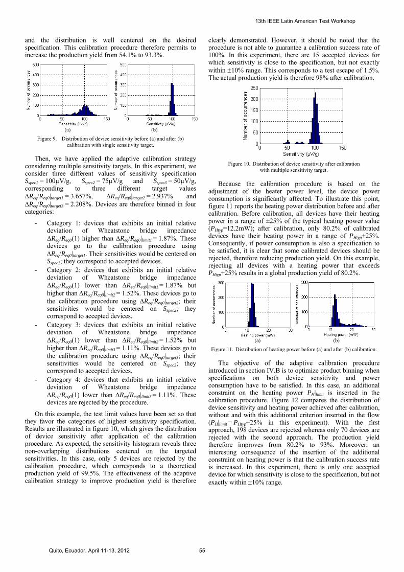
To illustrate this strategy, let us consider 2 different values of sensitivity specification Sspec1 and Sspec2 (with Sspec1 Sspec2), corresponding to 2 different target values Req/Req0|target1 and Req/Req0|target2. The related adaptive calibration flow is depicted in figure 7, which bins devices in three categories:
- Category 1: devices that exhibits an initial relative deviation of Wheatstone bridge impedance Req/Req0(1) higher than Req/Req0|limit1. These devices
Req/Req0|target
PHi PH
j PHk
device i
device j
device k
compute Req/Req0(1)
apply PH(0)=0 andmeasure IW(0)
apply PH(1)=50% and measure IW(1)
apply PH(2) and measure IW(2)
compute PH(3)
apply PH(3)
limiteq0
eq
eq0
eq
R
ΔR)1(
R
ΔR
device calibrated to Sspec
device k
no
yes
compute PH(2)
device rejected
13th IEEE Latin American Test Workshop
Quito, Ecuador, April 11-13, 2012 53
go to the calibration procedure using Req/Req0|target1. Their sensitivities would be centered on Sspec1; they correspond to accepted devices.
- Category 2: devices that exhibits an initial relative deviation of Wheatstone bridge impedance Req/Req0(1) lower than Req/Req0|limit1 but higher than Req/Req0|limit2. These devices go to the calibration procedure using Req/Req0|target2; their sensitivities would be centered on Sspec2; they correspond to accepted devices.
- Category 3: devices that exhibits an initial relative deviation of Wheatstone bridge impedance Req/Req0(1) lower than Req/Req0|limit2. These devices are rejected by the procedure.
Obviously, the number of categories can be freely chosen depending on the application. The test limit values have then to be adapted for each category.
Figure 7. Adaptive procedure for product binning with focus
on device sensitivity
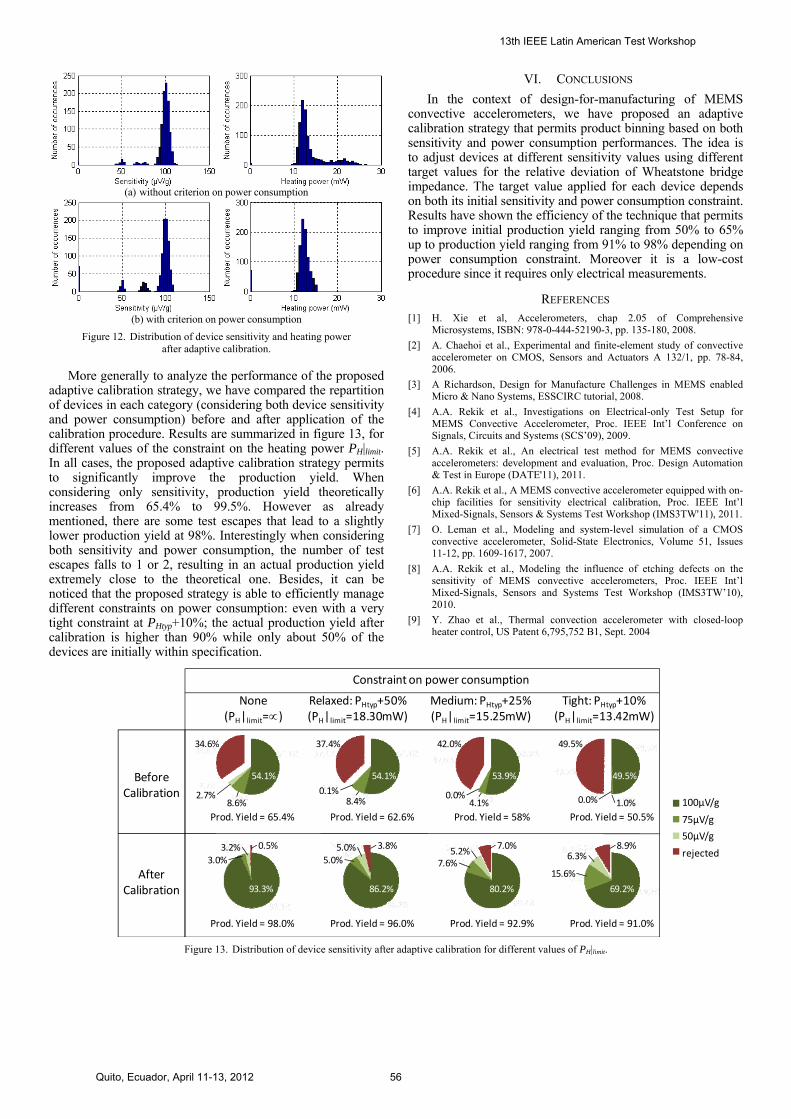
B. Binning on both device sensitivity and power consumption
Depending on the application, power consumption may be another important parameter in addition to sensitivity. Since the proposed calibration procedure is based on the adjustment of the heater power level, it is more than probable that for some circuits (especially circuits with very poor initial sensitivity), power consumption significantly increases after calibration.
In this context, a refinement of the calibration procedure consists in including an extra criterion on power consumption in addition to sensitivity calibration, as illustrated in the flow diagram of figure 8. In this procedure, each device is first directed for calibration towards the highest possible sensitivity
specification according the measurement of its initial relative deviation of Wheatstone bridge impedance, and then possibly redirected to lower sensitivity specification if power consumption constraints are not satisfied (we assume that most of the power consumption comes from the power dissipated in the heating element).
Figure 8. Adaptive procedure for product binning with focus on both
device sensitivity and power consumption
V. RESULTS
A number of simulations have been carried in order to evaluate the performances of the proposed adaptive calibration strategy. A population of 1,000 devices generated through Monte-Carlo simulations has been considered using the parametric fault model described in section II.
First, we have applied the original calibration procedure with a single sensitivity target. The objective was to calibrate devices to a nominal sensitivity Sspec = 100µV/g, which corresponds to a target value Req/Req0|target = 3.657% (determined from a simulation with all parameters at typical value). Results are illustrated in figure 9, which gives the distribution of device sensitivity before and after calibration. Initially, device sensitivity exhibits a rather large dispersion and only 541 out of 1,000 devices are within 10% nominal sensitivity specification. Applying the calibration procedure, 67 devices are actually rejected (with Req/Req0|limit = 1.87%), but the dispersion on device sensitivity is significantly reduced
compute Req/Req0(1)
apply PH(0)=0 andmeasure IW(0)
apply PH(1)=50% and measure IW(1)
apply PH(2) and measure IW(2)
compute PH(3)
apply PH(3)
limit1eq0
eq
eq0
eq
R
ΔR)1(
R
ΔR
device calibrated to Sspec1
device k
no
yes
compute PH(2)
target1eq0
eq
targeteq0
eq
R
ΔR
R
ΔRSet
apply PH(2) and measure IW(2)
compute PH(3)
apply PH(3)
limit2eq0
eq
eq0
eq
R
ΔR)1(
R
ΔR
device calibrated to Sspec2
no
yes
compute PH(2)
target2eq0
eq
targeteq0
eq
R
ΔR
R
ΔRSet
device rejected
compute Req/Req0(1)
apply PH(0)=0 andmeasure IW(0)
apply PH(1)=50% and measure IW(1)
apply PH(2) and measure IW(2)
compute PH(3)
apply PH(3)
limit1eq0
eq
eq0
eq
R
ΔR)1(
R
ΔR
device calibrated to Sspec1
device k
no
yes
compute PH(2)
target1eq0
eq
targeteq0
eq
R
ΔR
R
ΔRSet
apply PH(2) and measure IW(2)
compute PH(3)
apply PH(3)
limit2eq0
eq
eq0
eq
R
ΔR)1(
R
ΔR
device calibrated to Sspec2
no
yes
compute PH(2)
target2eq0
eq
targeteq0
eq
R
ΔR
R
ΔRSet
PH(2) PH|limit
no
yes
no
yes
PH(2) PH|limit
PH(3) PH|limit
no
yes
no
yes
PH(3) PH|limit
device rejected
no
no
device rejected
no
device rejected
13th IEEE Latin American Test Workshop
Quito, Ecuador, April 11-13, 2012 54
and the distribution is well centered on the desired specification. This calibration procedure therefore permits to increase the production yield from 54.1% to 93.3%.
(a) (b)
Figure 9. Distribution of device sensitivity before (a) and after (b) calibration with single sensitivity target.
Then, we have applied the adaptive calibration strategy considering multiple sensitivity targets. In this experiment, we consider three different values of sensitivity specification Sspec1 = 100µV/g, Sspec2 = 75µV/g and Sspec3 = 50µV/g, corresponding to three different target values Req/Req0|target1 = 3.657%, Req/Req0|target2 = 2.937% and Req/Req0|target3 = 2.208%. Devices are therefore binned in four categories:
- Category 1: devices that exhibits an initial relative deviation of Wheatstone bridge impedance ΔReq/Req0(1) higher than Req/Req0|limit1 = 1.87%. These devices go to the calibration procedure using Req/Req0|target1. Their sensitivities would be centered on Sspec1; they correspond to accepted devices.
- Category 2: devices that exhibits an initial relative deviation of Wheatstone bridge impedance ΔReq/Req0(1) lower than Req/Req0|limit1 = 1.87% but higher than Req/Req0|limit2 = 1.52%. These devices go to the calibration procedure using Req/Req0|target2; their sensitivities would be centered on Sspec2; they correspond to accepted devices.
- Category 3: devices that exhibits an initial relative deviation of Wheatstone bridge impedance ΔReq/Req0(1) lower than Req/Req0|limit2 = 1.52% but higher than Req/Req0|limit3 = 1.11%. These devices go to the calibration procedure using Req/Req0|target3; their sensitivities would be centered on Sspec3; they correspond to accepted devices.
- Category 4: devices that exhibits an initial relative deviation of Wheatstone bridge impedance ΔReq/Req0(1) lower than Req/Req0|limit3 = 1.11%. These devices are rejected by the procedure.
On this example, the test limit values have been set so that they favor the categories of highest sensitivity specification. Results are illustrated in figure 10, which gives the distribution of device sensitivity after application of the calibration procedure. As expected, the sensitivity histogram reveals three non-overlapping distributions centered on the targeted sensitivities. In this case, only 5 devices are rejected by the calibration procedure, which corresponds to a theoretical production yield of 99.5%. The effectiveness of the adaptive calibration strategy to improve production yield is therefore
clearly demonstrated. However, it should be noted that the procedure is not able to guarantee a calibration success rate of 100%. In this experiment, there are 15 accepted devices for which sensitivity is close to the specification, but not exactly within 10% range. This corresponds to a test escape of 1.5%. The actual production yield is therefore 98% after calibration.
Figure 10. Distribution of device sensitivity after calibration
with multiple sensitivity target.
Because the calibration procedure is based on the adjustment of the heater power level, the device power consumption is significantly affected. To illustrate this point, figure 11 reports the heating power distribution before and after calibration. Before calibration, all devices have their heating power in a range of ±25% of the typical heating power value (PHtyp=12.2mW); after calibration, only 80.2% of calibrated devices have their heating power in a range of PHtyp+25%. Consequently, if power consumption is also a specification to be satisfied, it is clear that some calibrated devices should be rejected, therefore reducing production yield. On this example, rejecting all devices with a heating power that exceeds PHtyp+25% results in a global production yield of 80.2%.
(a) (b)
Figure 11. Distribution of heating power before (a) and after (b) calibration.
The objective of the adaptive calibration procedure introduced in section IV.B is to optimize product binning when specifications on both device sensitivity and power consumption have to be satisfied. In this case, an additional constraint on the heating power PH|limit is inserted in the calibration procedure. Figure 12 compares the distribution of device sensitivity and heating power achieved after calibration, without and with this additional criterion inserted in the flow (PH|limit = PHtyp±25% in this experiment). With the first approach, 198 devices are rejected whereas only 70 devices are rejected with the second approach. The production yield therefore improves from 80.2% to 93%. Moreover, an interesting consequence of the insertion of the additional constraint on heating power is that the calibration success rate is increased. In this experiment, there is only one accepted device for which sensitivity is close to the specification, but not exactly within 10% range.
13th IEEE Latin American Test Workshop
Quito, Ecuador, April 11-13, 2012 55
(a) without criterion on power consumption
(b) with criterion on power consumption
Figure 12. Distribution of device sensitivity and heating power after adaptive calibration.
More generally to analyze the performance of the proposed adaptive calibration strategy, we have compared the repartition of devices in each category (considering both device sensitivity and power consumption) before and after application of the calibration procedure. Results are summarized in figure 13, for different values of the constraint on the heating power PH|limit. In all cases, the proposed adaptive calibration strategy permits to significantly improve the production yield. When considering only sensitivity, production yield theoretically increases from 65.4% to 99.5%. However as already mentioned, there are some test escapes that lead to a slightly lower production yield at 98%. Interestingly when considering both sensitivity and power consumption, the number of test escapes falls to 1 or 2, resulting in an actual production yield extremely close to the theoretical one. Besides, it can be noticed that the proposed strategy is able to efficiently manage different constraints on power consumption: even with a very tight constraint at PHtyp+10%; the actual production yield after calibration is higher than 90% while only about 50% of the devices are initially within specification.
VI. CONCLUSIONS
In the context of design-for-manufacturing of MEMS convective accelerometers, we have proposed an adaptive calibration strategy that permits product binning based on both sensitivity and power consumption performances. The idea is to adjust devices at different sensitivity values using different target values for the relative deviation of Wheatstone bridge impedance. The target value applied for each device depends on both its initial sensitivity and power consumption constraint. Results have shown the efficiency of the technique that permits to improve initial production yield ranging from 50% to 65% up to production yield ranging from 91% to 98% depending on power consumption constraint. Moreover it is a low-cost procedure since it requires only electrical measurements.
REFERENCES [1] H. Xie et al, Accelerometers, chap 2.05 of Comprehensive
Microsystems, ISBN: 978-0-444-52190-3, pp. 135-180, 2008.
[2] A. Chaehoi et al., Experimental and finite-element study of convective accelerometer on CMOS, Sensors and Actuators A 132/1, pp. 78-84, 2006.
[3] A Richardson, Design for Manufacture Challenges in MEMS enabled Micro & Nano Systems, ESSCIRC tutorial, 2008.
[4] A.A. Rekik et al., Investigations on Electrical-only Test Setup for MEMS Convective Accelerometer, Proc. IEEE Int’l Conference on Signals, Circuits and Systems (SCS’09), 2009.
[5] A.A. Rekik et al., An electrical test method for MEMS convective accelerometers: development and evaluation, Proc. Design Automation & Test in Europe (DATE'11), 2011.
[6] A.A. Rekik et al., A MEMS convective accelerometer equipped with on-chip facilities for sensitivity electrical calibration, Proc. IEEE Int’l Mixed-Signals, Sensors & Systems Test Workshop (IMS3TW'11), 2011.
[7] O. Leman et al., Modeling and system-level simulation of a CMOS convective accelerometer, Solid-State Electronics, Volume 51, Issues 11-12, pp. 1609-1617, 2007.
[8] A.A. Rekik et al., Modeling the influence of etching defects on the sensitivity of MEMS convective accelerometers, Proc. IEEE Int’l Mixed-Signals, Sensors and Systems Test Workshop (IMS3TW’10), 2010.
[9] Y. Zhao et al., Thermal convection accelerometer with closed-loop heater control, US Patent 6,795,752 B1, Sept. 2004
Figure 13. Distribution of device sensitivity after adaptive calibration for different values of PH|limit.
100µV/g
75µV/g
50µV/g
rejected
34.6%
54.1%
2.7%8.6%
54.1%
37.4%
0.1%8.4%
53.9%
42.0%
0.0%4.1%
49.5%
49.5%
0.0% 1.0%
93.3%
0.5%3.2%3.0%
86.2%
3.8%5.0%5.0%
80.2%
7.0%5.2%
7.6%
69.2%
8.9%6.3%
15.6%
Before Calibration
After Calibration
Relaxed: PHtyp+50%(PH|limit=18.30mW)
Constraint on power consumption
Medium: PHtyp+25%(PH|limit=15.25mW)
Tight: PHtyp+10%(PH|limit=13.42mW)
None(PH|limit=)
Prod. Yield = 65.4% Prod. Yield = 62.6% Prod. Yield = 58% Prod. Yield = 50.5%
Prod. Yield = 98.0% Prod. Yield = 96.0% Prod. Yield = 92.9% Prod. Yield = 91.0%
13th IEEE Latin American Test Workshop
Quito, Ecuador, April 11-13, 2012 56