Embed Size (px)
Citation preview

Lab 4 - Operational Amplifiers 1
Gain
ReadMeFirst
Lab Summary
There are three basic configurations for operational amplifiers. If the amplifier is multiplying the amplitude of the signal, the multiplication factor is called gain. If the amplitude of a signal is reduced at any time it is referred to as attenuation. The two gain configurations you will build are the inverting and non-inverting stages. A third configuration, the unity gain stage, or buffer, is often used to isolate signals and provide additional current capability. There is a limit to the maximum frequency that any op amp can pass without distortion. Moreover, as the gain of an op amp is increased, the maximum frequency that can be amplified without distortion is reduced. This characteristic is the called the Gain Bandwidth Product and is due to the limitation of the Slew Rate of the op amp. The slew rate, usually in Volts / microseconds, is how fast the signal can change and is limited by the internal capacitance of the device.
Lab Preparation
Please review the following material from previous and current labs before attempting this lab:
1. Review the Introduction to Lab Equipment for operational instructions of the Rigol Triple Output Power Supply.
2. Review Active_Filter_I_Notes.pdf for more background on analog filters.
3. Familiarize yourself with the LME49710NA OP Amp datasheet as it will be
referred to throughout the lab.
Videos: Operational Amplifiers 1.mp4
Lab Supplies
You will need the following supplies for the lab.
1. Bread board and jumper wire kit 2. The following components
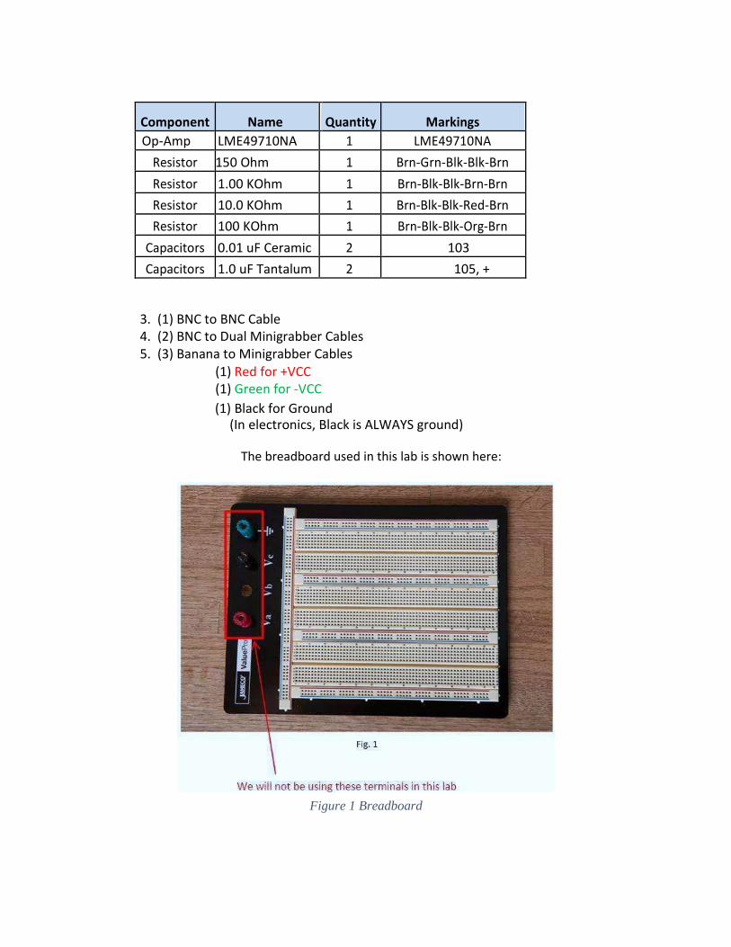
Figure 1 Breadboard
Component Name Quantity Markings
Op-Amp LME49710NA 1 LME49710NA
Resistor 150 Ohm 1 Brn-Grn-Blk-Blk-Brn
Resistor 1.00 KOhm 1 Brn-Blk-Blk-Brn-Brn
Resistor 10.0 KOhm 1 Brn-Blk-Blk-Red-Brn
Resistor 100 KOhm 1 Brn-Blk-Blk-Org-Brn
Capacitors 0.01 uF Ceramic 2 103
Capacitors 1.0 uF Tantalum 2 105, +
3. (1) BNC to BNC Cable
4. (2) BNC to Dual Minigrabber Cables
5. (3) Banana to Minigrabber Cables
(1) Red for +VCC (1) Green for -VCC (1) Black for Ground
(In electronics, Black is ALWAYS ground)
The breadboard used in this lab is shown here:
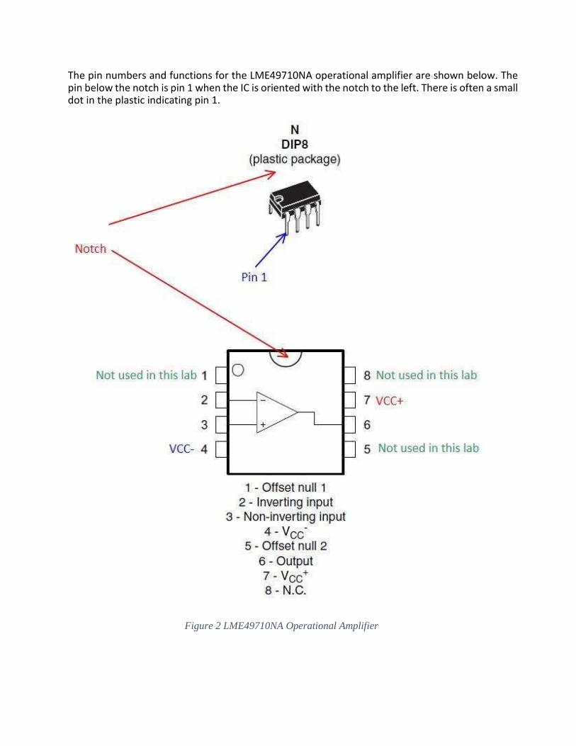
Figure 2 LME49710NA Operational Amplifier
The pin numbers and functions for the LME49710NA operational amplifier are shown below. The pin below the notch is pin 1 when the IC is oriented with the notch to the left. There is often a small dot in the plastic indicating pin 1.
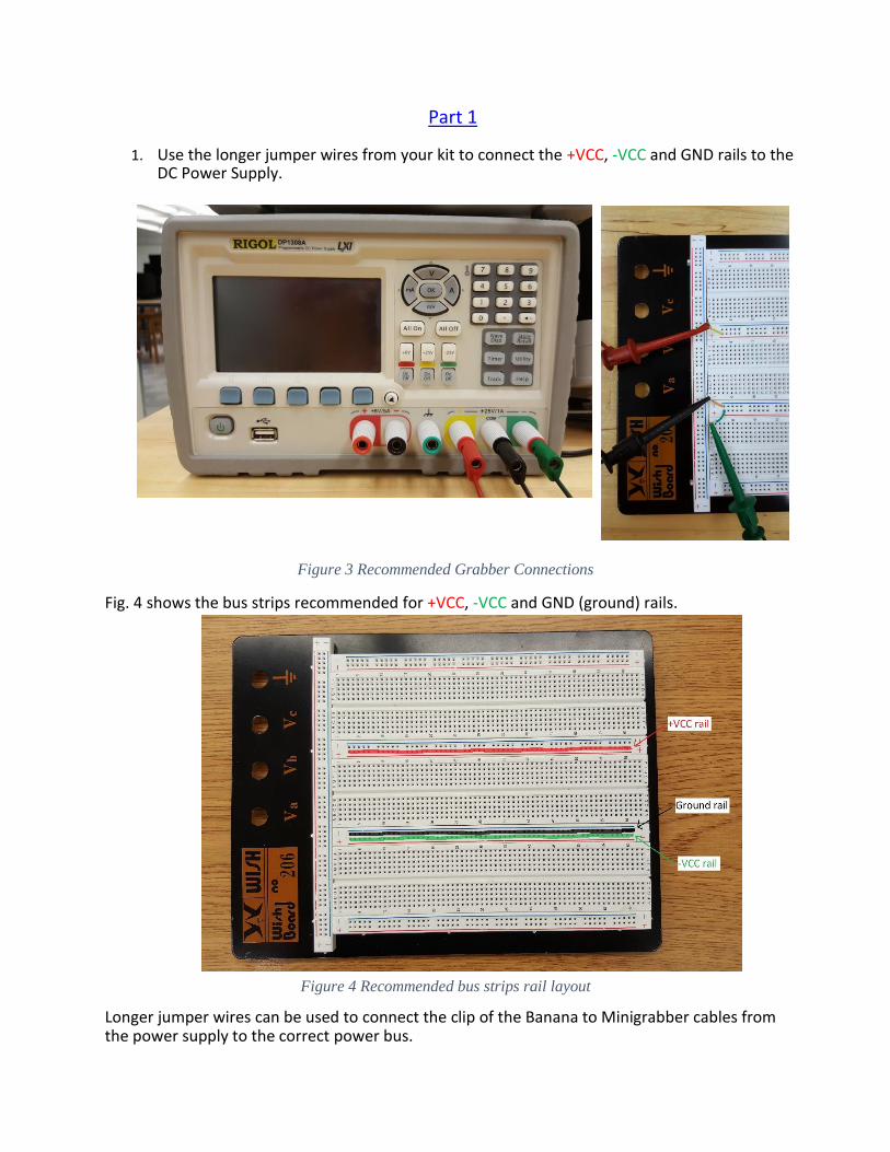
Figure 3 Recommended Grabber Connections
Figure 4 Recommended bus strips rail layout
Part 1
1. Use the longer jumper wires from your kit to connect the +VCC, -VCC and GND rails to the DC Power Supply.
Fig. 4 shows the bus strips recommended for +VCC, -VCC and GND (ground) rails.
Longer jumper wires can be used to connect the clip of the Banana to Minigrabber cables from the power supply to the correct power bus.
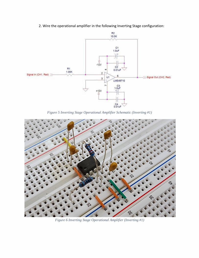
Figure 5 Inverting Stage Operational Amplifier Schematic (Inverting #1)
2. Wire the operational amplifier in the following Inverting Stage configuration:
Figure 6 Inverting Stage Operational Amplifier (Inverting #1)
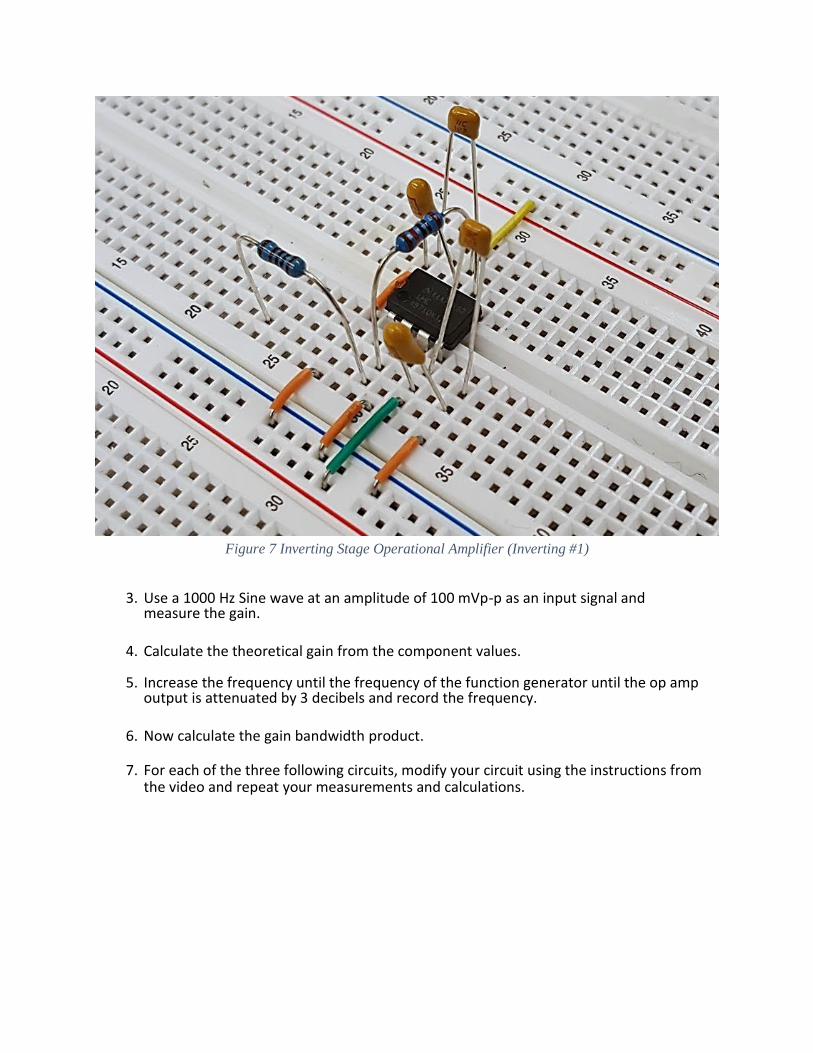
3. Use a 1000 Hz Sine wave at an amplitude of 100 mVp-p as an input signal and measure the gain.
4. Calculate the theoretical gain from the component values.
5. Increase the frequency until the frequency of the function generator until the op amp output is attenuated by 3 decibels and record the frequency.
6. Now calculate the gain bandwidth product.
7. For each of the three following circuits, modify your circuit using the instructions from the video and repeat your measurements and calculations.
Figure 7 Inverting Stage Operational Amplifier (Inverting #1)

Figure 8 Inverting Stage Operational Amplifier Schematic (Inverting #2)
Figure 9 Non-Inverting Stage Operational Amplifier Schematic (Non-Inverting #1)
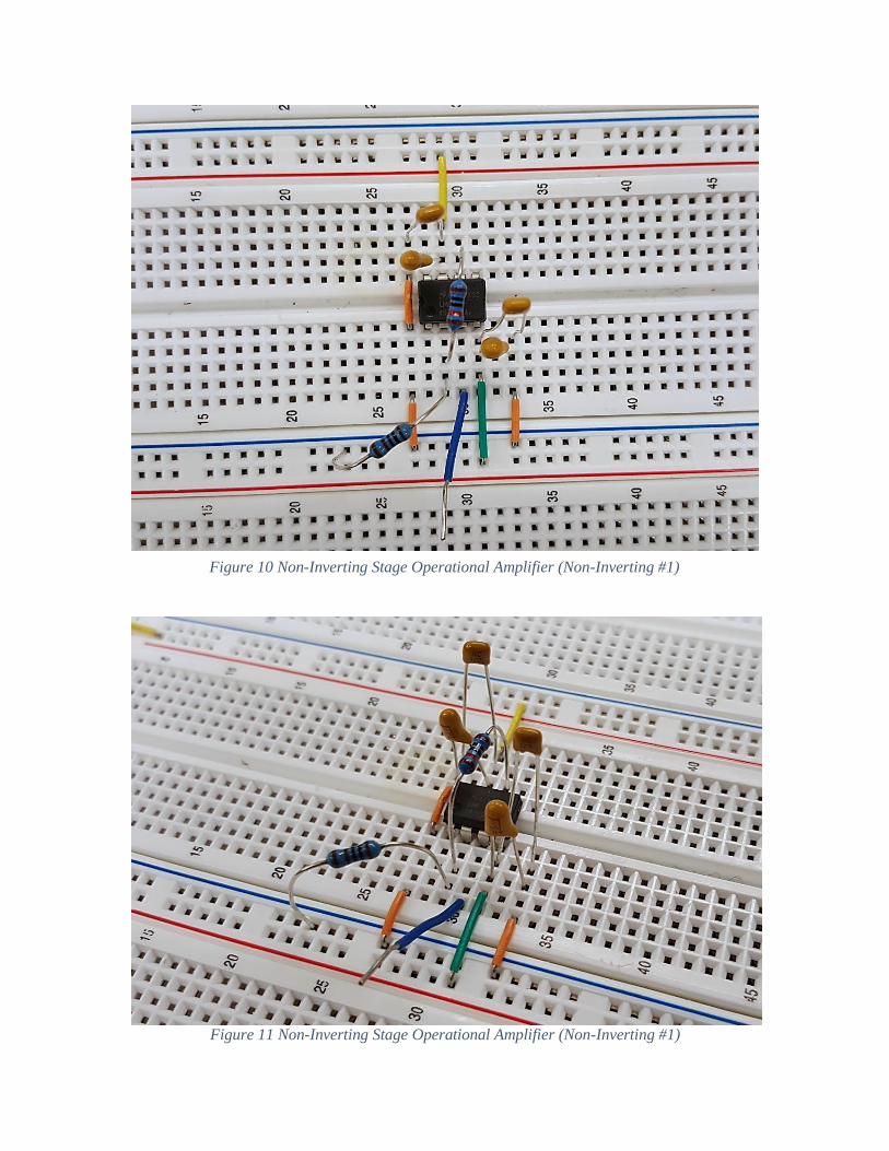
Figure 11 Non-Inverting Stage Operational Amplifier (Non-Inverting #1)
Figure 10 Non-Inverting Stage Operational Amplifier (Non-Inverting #1)
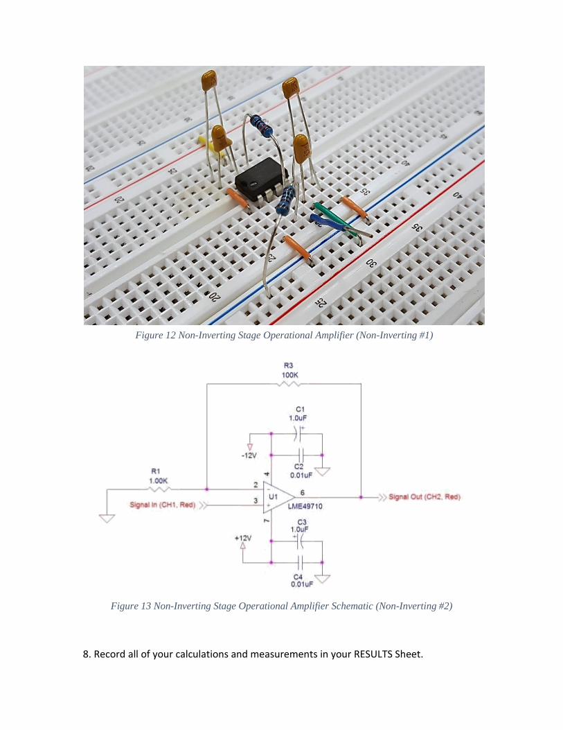
8. Record all of your calculations and measurements in your RESULTS Sheet.
Figure 12 Non-Inverting Stage Operational Amplifier (Non-Inverting #1)
Figure 13 Non-Inverting Stage Operational Amplifier Schematic (Non-Inverting #2)
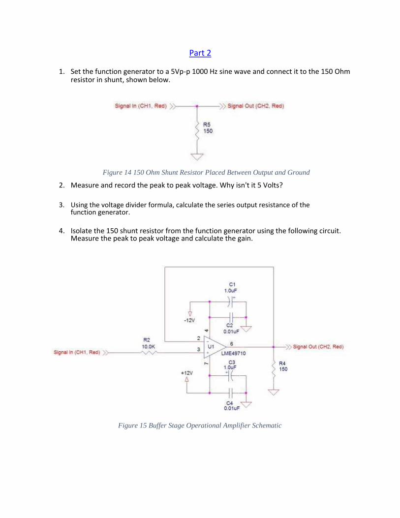
Figure 14 150 Ohm Shunt Resistor Placed Between Output and Ground
Figure 15 Buffer Stage Operational Amplifier Schematic
Part 2
1. Set the function generator to a 5Vp-p 1000 Hz sine wave and connect it to the 150 Ohm resistor in shunt, shown below.
2. Measure and record the peak to peak voltage. Why isn't it 5 Volts?
3. Using the voltage divider formula, calculate the series output resistance of the
function generator.
4. Isolate the 150 shunt resistor from the function generator using the following circuit.
Measure the peak to peak voltage and calculate the gain.

*** END of LAB ***
Figure 16 Buffer Stage Operational Amplifier
Figure 17 Buffer Stage Operational Amplifier