Embed Size (px)
Citation preview

www.semiconductordigest.com
SEMICONDUCTORS | AI | DESIGN | PACKAGING | MEMS | DISPL AYS
MARCH 2021
TSMC’s Technology Roadmap p. 22
New Drivers Propelling Semis, Equipment, IP p. 25
The Future of Compute p. 27
Multilayer Thickness Evaluation by Picosecond Ultrasonics p. 31
Mid-Infrared Optical Metrology FOR HIGH ASPECT RATIO HOLES PAGE 16

16 | March 2021 Semiconductor Digest www.semiconductordigest.com
Metrology
Mid-Infrared Optical Metrology for High Aspect Ratio Holes in 3D NAND Memory ManufacturingG. ANDREW ANTONELLI, O n t o I n n o v a t i o n , BO HUI NG a n d SADAO TAKABAYASHI, M i c r o n Te c h n o l o g y
Infrared critical dimension metrology (IRCD) addresses the shortcomings of conventional ultraviolet to near-infrared OCD in channel hole etch high-fidelity z-profile and amorphous carbon hardmask etch BCD metrology.
A NEW METROLOGY SYSTEM USES
spectroscopic ellipsometry at mid-infrared wavelengths
to provide accurate critical dimension and profile measurements of high-as-pect-ratio (HAR) holes in 3D NAND memory. This information is essential for developing and controlling the fabrication process. The non-destructive technique exploits unique optical prop-erties of mid-IR radiation to extract information that has not previously been available on a robust platform suitable for in-fab use. We look at two examples: channel holes, which have aspect ratios as high as 60:1 and eventually become vertical strings of memory cells in 3d NAND memory, and the holes in the hardmask, which have aspect ratios up to 25:1 and are used to etch the channel holes.
Ellipsometric optical critical dimension (OCD) metrology in the ul-traviolet to near infrared (190 nm to 1.7
m) spectral range is a well-established
process control technique. It can measure buried features inaccessible to top-down non-destructive optical,
electron, or ion imaging techniques, but it has limitations when applied to the extreme 3D and high aspect ratio features of 3D NAND devices. As more devices become inherently
three-dimensional and scale vertically, the ability to measure the exact dimen-sions of buried features and re-entrant
geometries will become increasingly important.
The transistor channel strings in the most advanced 3D NAND devices begin as high-aspect ratio holes (hereafter channel holes) etched through a stack of alternating silicon dioxide and silicon nitride (or poly-silicon) layers with 128 or more layer-pairs. Etching holes with 100 nm diameters and depths greater than 6 m (aspect ratios greater than 60:1) is challenging. The etch process uses a hard mask with holes of similar diameter and depths up 2.5 microns, giving them aspect ratios of 25:1 and presenting challenges similar to the channel hole etch. Figure 1 illustrates
these structures schematically. An ideal etch process would yield a perfectly cylindrical hole with a uniform circular profile along its full length across the entire surface of a 300mm wafer.
Figure 1. Representative structures under investigation for the (a) channel hole etch and (b) hardmask etch operations. These structures have a > 150 pair superlattice of silicon dioxide and silicon nitride with a pair thickness of ~50 nm, a hole diameter of ~ 100 nm, and amorphous carbon hardmask thickness > 2 m.

www.semiconductordigest.com Semiconductor Digest March 2021 | 17
Realizable etch processes show sig-nificant deviations from cylindrical profiles both within a wafer and from wafer to wafer. Developing and con-trolling these processes requires the ability to measure hole profiles. Having this measurement capability inline accelerates process learning during the device development stage and is also critical even after the process has been transferred to high volume manufac-turing where it proliferates to more etch chambers.
OCD measurements are indirect. They
begin with a simulation process that predicts expected effects on measured optical parameters when light is reflected (or transmitted) from a model structure. Ideally, unique effects are found that correlate uniquely to the physical mea-surement of interest. On channel holes, conventional OCD metrology tools using UV to near IR wavelengths provide accurate and robust measurements for hole volume and in some cases the tilt of the channel hole at each point on the wafer but are typically incapable of de-termining the shape of the channel hole
profile due to the high level of spectral correlation. In use, OCD models can be constrained to provide adequate process feedback when z-profile variation from site to site is low, but constrained models are insufficient when the site-to-site or wafer-to-wafer channel hole shape vari-ation is large and when process schemes change dynamically, as often occurs during the development stage. Adapting to changes in the process is further hin-dered by the considerable time required to model new solutions. A more flexible metrology solution would cover a wider range of z-profile variations and allow faster modelling (on the order of days) to keep up with the fast-paced development environment in a semiconductor fab.
The most popular amorphous carbon used as a hardmask in these integration schemes is graphitic in-character and optically opaque in the traditional OCD spectral range, limiting OCD metrology to the top surface. Ideally, the metrology technique should receive signal from the entire etched amorphous carbon structure, including the bottom, and be capable of z-profile extraction. Although the amorphous carbon is sacrificial, its profile and particularly its bottom CD (BCD) strongly affect the channel CD profile and must be adequately controlled. Currently, there is no established nonde-structive inline technique for amorphous
Figure 2. Optical penetration depth in the mid-infrared spectral range of typical silicon dioxide and silicon nitride materials.
Figure 3. Simulated mid-infrared spectral response change of the M33 and M34 Mueller matrix elements for a 1 nm increase in CD at different heights on the channel hole, where 0% indicates the bottom and 100% indicates the top.
Metrology
18 | March 2021 Semiconductor Digest www.semiconductordigest.com
carbon hardmask BCD metrology in either the development or production phases of 3D NAND manufacturing.
To address these HAR etch process monitoring challenges a mid-infrared spectroscopic ellipsometer, Aspect™ (Onto Innovation) was constructed to perform infrared critical dimension metrology (IRCD). Infrared ellipsometry is by no means a new concept and has been useful as a laboratory technique, but previous implementations have had significant limitations in terms of measurement speed, vibration sensitivity,
and component fragility. Aspect enables fast, high signal-to-noise ratio measure-ments using a novel high-brightness infrared light source and a non-cryogenic spectroscopic detector array suitable for in-line production measurements. The objectives as well as the polarization and compensation elements are optimized for long term operation in the mid-infrared. The optical system has been designed to mitigate spurious reflections from the back side of the wafer, which, at low doping levels, is transparent in the mid-infrared range. The initial product
release has a probe size less than 100 m and outputs the M33 and M34 Mueller matrix elements. i.e., and or C and S. A smaller probe size and access to more Mueller elements will be available in future revisions of the tool.
Channel hole etchTypically, silicon dioxide and silicon nitride are largely transparent in the ultraviolet to near-infrared spectral range. Light within this wavelength range can propagate through the entire 3D NAND stack before reflecting at
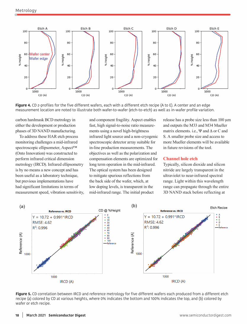
Figure 4. CD z-profiles for the five different wafers, each with a different etch recipe (A to E). A center and an edge measurement location are noted to illustrate both wafer-to-wafer (etch-to-etch) as well as in-wafer profile variation.
Figure 5. CD correlation between IRCD and reference metrology for five different wafers each produced from a different etch recipe (a) colored by CD at various heights, where 0% indicates the bottom and 100% indicates the top, and (b) colored by wafer or etch recipe.

Metrology
www.semiconductordigest.com Semiconductor Digest March 2021 | 19
the surface of the silicon substate (or the first reflective layer, counting from top to bottom). Therefore, while there is sensitivity from the top to the bottom of the structure, the signals are mixed and not unique – every wavelength carries roughly the same information about the top area and the bottom area. This physical property manifests in model parameter correlation issues that result in inability to determine the profile of the channel hole unless the model is constrained appropriately: only the volume is a robust measurement. Therefore, the key to measuring vertical z-profiles with a spectroscopic tech-nique is to have different wavelengths carrying information from different depths of the channel hole.
Figure 2 plots penetration depth versus wavelength for silicon dioxide and silicon nitride. Absorption bands in these dielectrics induce variations in transmission. The regions with the shortest penetration depth yield the most surface-sensitive information, and the long penetration depths yield BCD information. Another way to illustrate the physical phenomenon is through spectral sensitivity simulations at different heights of a channel string hole. Figure 3 illustrates the spectral sensitivity at different heights. The unique signatures strongly suggest the capability of extracting different CDs
separately at different heights with minimal parameter correlation.
Controlling and minimizing vertical, within-wafer and wafer-to-wafer CD uniformity is a goal of all HAR etches; therefore, during the development stages, HAR etch recipes are constantly revised and changed. The ideal metrology would provide solutions that are robust against such process changes – a perennial challenge for nondestructive indirect measurement methods. Direct imaging techniques are usually not affected by process changes, but because of their destructive nature, can generally be used only as reference metrology for the development of nondestructive solu-tions, rather than as standalone in-line metrology.
The depth sensitivity illustrated in Figures 2 and 3 provides the basis for IRCD z-profile metrology. To demon-strate the value of the technology, wafers with multiple etch recipes that lead to varying z-profiles were prepared and characterized with destructive imaging metrology to acquire reference data to evaluate the IRCD
solution accuracy. Figure 4 shows typical etch profiles of five wafers, all with different etch recipes, illustrating recipe-to-recipe as well as wafer center-to-edge variation. The desired metrology technique needs to detect such differences.
Figure 5 shows the correlation of IRCD measured values versus reference data pooled across multiple points per wafer spread uniformly, in location, across multiple wafers and etch recipes, and from the top to the bottom of the channel. There is Angstrom-level disagreement as represented by the correlation root-mean-squared error (RMSE) – note that typical CD values are roughly 1000Å. Figure 5a groups the data by CDs at various heights, showing that IRCD is measuring individual CDs as well as their in-wafer and wafer-to-wafer variation with high accuracy. Figure 5b groups the data by wafer, confirming for each wafer and each recipe IRCD is measuring the z-profile with high fidelity. Figure 6 presents an alternative illustration of the z-profile differences from one etch recipe to another as well as their radial, wafer-location dependence. It shows that IRCD can capture the many CD variations pertinent to in-line HAR process development and control.
Figure 7 shows the precision values pooled from 12 sites and 5 cycles for the CDs at various heights expressed
Figure 7. CD precision expressed as 3sigma as a % of the average CD measured at different heights of the channel hole.
Figure 6. Radial dependence of CDs at different heights along the channel hole for wafer processed by different etch recipes.

Metrology
20 | March 2021 Semiconductor Digest www.semiconductordigest.com
as 3sigma, where sigma is the standard deviation of the measurements of a single point. The data demonstrate Angstrom-level precision with uncer-tainties 0.2% of the nominal CD values. Good precision is a typical attribute of ellipsometry measurements. In ad-dition, from the modeling perspective, to preserve precision, we also employ mathematically complete functions to express the channel hole profile that are stable for regression algorithms for ex-perimental data fitting. As functions are modeled, there is no limit to the number of reported CDs at various heights.
Carbon hardmask etchThe 3D NAND channel hole patterning currently uses an amorphous carbon hardmask, which is itself an HAR hole structure. The thickness of the hardmask in most 3D NAND patterning schemes is 2 m or greater. Figure 8 plots optical penetration depth in the ultraviolet to near-infrared and the mid-infrared for a typical graphitic amorphous carbon hardmask material. The increase in optical penetration with increasing wavelength is a general feature of these hardmask materials. The low penetration depth in the ultraviolet to the near-infrared
spectral range makes even blanket film thickness measurement nearly impos-sible at production targets. However, there is an order of magnitude increase in the optical penetration in the mid-in-frared, implying greater measurement capability.
Because of the lack of probe sensitivity at production thicknesses of graphitic amorphous carbon hardmask films and structures, the most critical feature of a useful metrology technique is sufficient probe penetration. In a reflective tech-nique, as is common for ellipsometry, op-tical penetration generally needs to occur over at least two pathlengths. Figure 9
Figure 9. Measured Mueller matrix elements (M33 on left and M34 on right) of a typical amorphous carbon hardmask etch structures. The blue curves are the experimentally measured signals, and the red curves are from IRCD model calculations.
Figure 8. Optical penetration depth in the (a) ultraviolet to near-infrared and the (b) mid-infrared spectral regimes of typical graphitic amorphous carbon hardmask materials.
Metrology
www.semiconductordigest.com Semiconductor Digest March 2021 | 21
shows a typical IRCD spectrum from an etched amorphous carbon hardmask with film thickness >2.5 m, typical of advanced node 3D NAND structures, that is on top of a 3D NAND silicon dioxide and silicon nitride superlattice exceeding 5 m. The oscillations visible from 5000-8000 nm in spectral range are thickness fringes of the superlattice, indicating light penetration through not only the amorphous carbon layer but also the entire 3D NAND stack. The lack of oscillations beyond 8000 nm wavelength is due to the absorption bands of the silicon dioxide and silicon nitride.
Alternatively, we can illustrate the light interaction by a sensitivity simulation of a thickness change in amorphous carbon, as in Figure 10. The spectral sensitivity covers the entire wavelength range. Even in the flat portion of the spectral regime (8000-10500 nm) there is optical penetration into the amorphous carbon layer, with a reflection at the amorphous carbon interface with the 3D NAND stack.
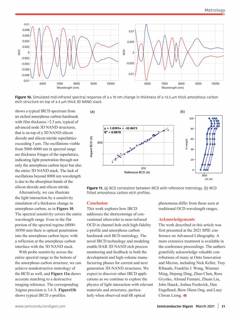
With probe sensitivity across the entire spectral range to the bottom of the amorphous carbon structure, we can achieve nondestructive metrology of the BCD as well, and Figure 11a shows accurate matching to a destructive imaging reference. The corresponding 3sigma precision is 3.4 Å. Figure11b shows typical IRCD z-profiles.
ConclusionThis work explores how IRCD addresses the shortcomings of con-ventional ultraviolet to near-infrared OCD in channel hole etch high-fidelity z-profile and amorphous carbon hardmask etch BCD metrology. The novel IRCD technology and modeling enable HAR 3D NAND etch process monitoring and feedback in both the development and high-volume manu-facturing phases for current and next generation 3D-NAND structures. We expect to discover other IRCD appli-cations as we continue to explore the physics of light interaction with relevant materials and structures, particu-larly when observed mid-IR optical
phenomena differ from those seen at traditional OCD wavelength ranges.
AcknowledgementsThe work described in this article was first presented at the 2021 SPIE con-ference on Advanced Lithography. A more extensive treatment is available in the conference proceedings. The authors gratefully acknowledge valuable con-tributions of many at Onto Innovation and Micron, including Nick Keller, Troy Ribaudo, Franklin J. Wong, Wenmei Ming, Hepeng Ding, Zhuo Chen, Ross Grynko, Ahmad Fumani, Zhuan Liu, John Hauck, Joshua Frederick, Dan Engelhard, Biow Hiem Ong, and Luey Chwan Liong.
Figure 10. Simulated mid-infrared spectral response of a ± 10 nm change in thickness of a >2.5 m thick amorphous carbon etch structure on top of a 6 m thick 3D NAND stack.
Figure 11. (a) BCD correlation between IRCD with reference metrology. (b) IRCD fitted amorphous carbon etch profiles.