Embed Size (px)
Citation preview
Project Two
RISC Processor Implementation
ECE 485
Chenqi BaoPeter Chinetti
November 6, 2013
Instructor: Professor Borkar
1 Statement of Problem
This project requires the design and test of a RISC processor in VHDL. It fo-cuses especially on the datapath design of the processor, and its implementation.In this groups’ specific case, the required instructions1 were:
Name Abrev. TypeLoad Word lw IStore Word sw IAdd add RBranch On Equal beq INAND nand ROR Immediate ori IOR or RAND Immediate andi I
2 Background
2.1 Instruction Types
The MIPS ISA defines three instruction types, R, I, and J type instructions.Only R and I type instructions will be covered here, as they are the only in-structions that are to be implemented for this project.
1NAND does not exist in the MIPS ISA, so the ISA was extrapolated to fill out the table
1
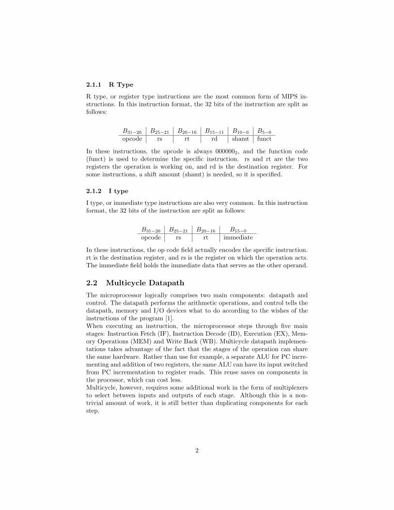
2.1.1 R Type
R type, or register type instructions are the most common form of MIPS in-structions. In this instruction format, the 32 bits of the instruction are split asfollows:
B31−26 B25−21 B20−16 B15−11 B10−6 B5−0
opcode rs rt rd shamt funct
In these instructions, the opcode is always 0000002, and the function code(funct) is used to determine the specific instruction. rs and rt are the tworegisters the operation is working on, and rd is the destination register. Forsome instructions, a shift amount (shamt) is needed, so it is specified.
2.1.2 I type
I type, or immediate type instructions are also very common. In this instructionformat, the 32 bits of the instruction are split as follows:
B31−26 B25−21 B20−16 B15−0
opcode rs rt immediate
In these instructions, the op code field actually encodes the specific instruction.rt is the destination register, and rs is the register on which the operation acts.The immediate field holds the immediate data that serves as the other operand.
2.2 Multicycle Datapath
The microprocessor logically comprises two main components: datapath andcontrol. The datapath performs the arithmetic operations, and control tells thedatapath, memory and I/O devices what to do according to the wishes of theinstructions of the program [1].When executing an instruction, the microprocessor steps through five mainstages: Instruction Fetch (IF), Instruction Decode (ID), Execution (EX), Mem-ory Operations (MEM) and Write Back (WB). Multicycle datapath implemen-tations takes advantage of the fact that the stages of the operation can sharethe same hardware. Rather than use for example, a separate ALU for PC incre-menting and addition of two registers, the same ALU can have its input switchedfrom PC incrementation to register reads. This reuse saves on components inthe processor, which can cost less.Multicycle, however, requires some additional work in the form of multiplexersto select between inputs and outputs of each stage. Although this is a non-trivial amount of work, it is still better than duplicating components for eachstep.
2
2.3 VHDL
VHDL is a hardware description language that can be used to prototype dig-ital systems. According to [2], “VHDL includes facilities for describing logicalstructure and function of digital system at a number of levels of abstraction,from system level down to the gate level.”
3 Implementation
3.1 Design Decisions
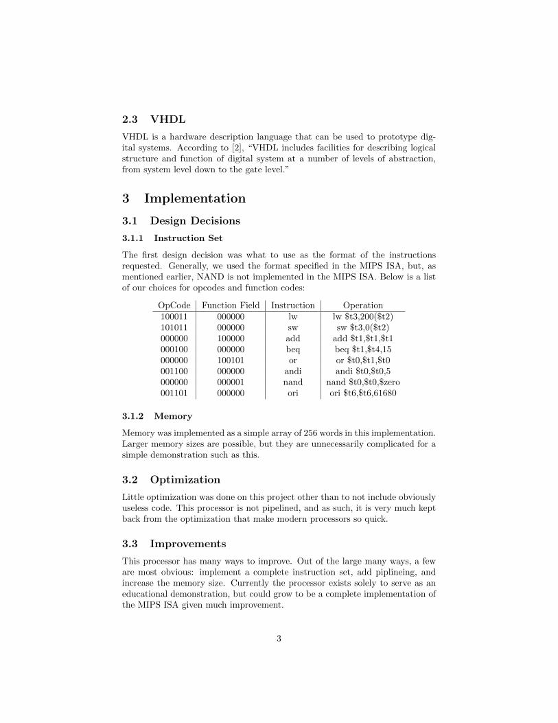
3.1.1 Instruction Set
The first design decision was what to use as the format of the instructionsrequested. Generally, we used the format specified in the MIPS ISA, but, asmentioned earlier, NAND is not implemented in the MIPS ISA. Below is a listof our choices for opcodes and function codes:
OpCode Function Field Instruction Operation100011 000000 lw lw $t3,200($t2)101011 000000 sw sw $t3,0($t2)000000 100000 add add $t1,$t1,$t1000100 000000 beq beq $t1,$t4,15000000 100101 or or $t0,$t1,$t0001100 000000 andi andi $t0,$t0,5000000 000001 nand nand $t0,$t0,$zero001101 000000 ori ori $t6,$t6,61680
3.1.2 Memory
Memory was implemented as a simple array of 256 words in this implementation.Larger memory sizes are possible, but they are unnecessarily complicated for asimple demonstration such as this.
3.2 Optimization
Little optimization was done on this project other than to not include obviouslyuseless code. This processor is not pipelined, and as such, it is very much keptback from the optimization that make modern processors so quick.
3.3 Improvements
This processor has many ways to improve. Out of the large many ways, a feware most obvious: implement a complete instruction set, add piplineing, andincrease the memory size. Currently the processor exists solely to serve as aneducational demonstration, but could grow to be a complete implementation ofthe MIPS ISA given much improvement.
3

3.4 Failures
Thankfully, we have no failures to report.
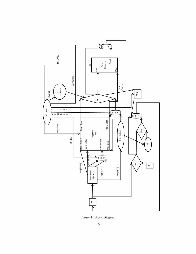
3.5 Block Diagram
See figure 1.
3.6 Simulation
The output of the simulations can be found in figures 2-9. The simulation wasdone sequentially, in the order of presentation, so the values going into subse-quent instructions are often dependent on the output of the previous command.
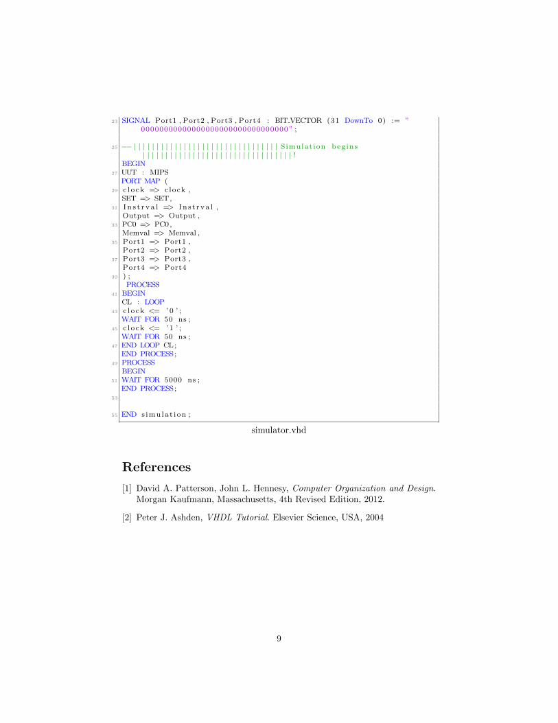
3.7 Code Listing
3.7.1 Datapath
1 e n t i t y MIPS i sPort (
3 c l o ck : in b i t ; −−c l o ck recordPC0 : out i n t e g e r ; −−PC counter (32 b i t s)
5 SET : in b i t ;Memval : out b i t v e c t o r (31 downto 0) ; −−mem wordaddre s sab l e
7 I n s t r v a l : out b i t v e c t o r (31 downto 0) ; −−I n s t r u c t i o n 32b i t s wideOutput : out BIT VECTOR (31 downto 0) ; −−We are working inWord s i z e
9 Port1 , Port2 , Port3 , Port4 : out b i t v e c t o r (31 downto 0) ) ;end MIPS ;
11
a r c h i t e c t u r e INSTRUCTION of MIPS i s13 −−−−−−−−−−−−−−−−−−−−−− Data types
s i g n a l i n t e r n a l s t a t e : i n t e g e r ;15 subtype word i s b i t v e c t o r (31 downto 0) ; −− 32−b i t words
type r e g f i l e i s array (0 to 31) o f word ; −− 32 words17 type ram i s array (0 to 255) o f word ; −− toy s i z e d ram f o r t e s t i n g
subtype reg addr i s b i t v e c t o r (4 downto 0) ; −− 2ˆ5 can s t o r e 32r eg s
19 subtype hal fword i s b i t v e c t o r (15 downto 0) ; −− 16−b i t e n t i t i e s i . e. Immediate va lue
subtype byte i s b i t v e c t o r (7 downto 0) ; −− i f we need bytes21 constant bvc : b i t v e c t o r (0 to 1) := ”01” ; −−Binary value−−−−−−−−−−−−−−−−−−i n t −> b i t s
23 procedure i n t 2 b i t s ( i n t : in i n t e g e r ; b i t s : out b i t v e c t o r ) i sv a r i a b l e temp : i n t e g e r ;
25 v a r i a b l e r e s u l t : b i t v e c t o r ( b i t s ’ range ) ;begin
27 temp := i n t ;i f i n t < 0 then
29 temp := − i n t − 1 ;
4
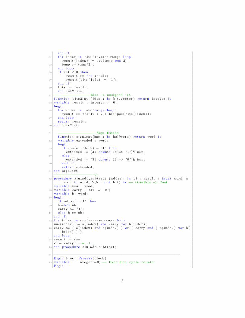
end i f ;31 f o r index in b i t s ’ r e v e r s e r a n g e loop
r e s u l t ( index ) := bvc ( temp rem 2) ;33 temp := temp/2 ;
end loop ;35 i f i n t < 0 then
r e s u l t := not r e s u l t ;37 r e s u l t ( b i t s ’ l e f t ) := ’ 1 ’ ;
end i f ;39 b i t s := r e s u l t ;
end i n t 2 b i t s ;41 −−−−−−−−−−−−−−−−−−b i t s −> unsigned i n t
func t i on b i t s 2 i n t ( b i t s : in b i t v e c t o r ) re turn i n t e g e r i s43 v a r i a b l e r e s u l t : i n t e g e r := 0 ;
begin45 f o r index in b i t s ’ range loop
r e s u l t := r e s u l t ∗ 2 + bit ’ pos ( b i t s ( index ) ) ;47 end loop ;
re turn r e s u l t ;49 end b i t s 2 i n t ;
51 −−−−−−−−−−−−−−−−−− Sign Extendfunc t i on s i g n e x t (imm : in hal fword ) re turn word i s
53 v a r i a b l e extended : word ;begin
55 i f imm(imm’ l e f t ) = ’1 ’ thenextended := (31 downto 16 => ’ 1 ’ )& imm;
57 e l s eextended := (31 downto 16 => ’ 0 ’ )& imm;
59 end i f ;r e turn extended ;
61 end s i g n e x t ;−−−−−−−−−−−−−−−−−−−+/−
63 procedure a lu add subt ra c t ( addse l : in b i t ; r e s u l t : inout word ; a ,nb : in word ; V,N : out b i t ) i s −− Overflow −> Cout
v a r i a b l e sum : word ;65 v a r i a b l e car ry : b i t := ’ 0 ’ ;
v a r i a b l e b : word ;67 begin
i f addse l = ’1 ’ then69 b:=Not nb ;
car ry := ’ 1 ’ ;71 e l s e b := nb ;
end i f ;73 f o r index in sum ’ r e v e r s e r a n g e loop
sum( index ) := a ( index ) xor car ry xor b( index ) ;75 car ry := ( a ( index ) and b( index ) ) or ( car ry and ( a ( index ) xor b(
index ) ) ) ;end loop ;
77 r e s u l t := sum ;V := carry ;−−= ’ 1 ’ ;
79 end procedure a lu add subt ra c t ;
81 −−−−−−−−−−−−−−−−−−−−−−−−−−−−−−−−−−−−−−−−−−−−−−−−−−−−−−−−−−−−−−Begin Proc : Process ( c l o ck )
83 v a r i a b l e i : i n t e g e r :=0; −− Execution c y c l e counterBegin
5
85 i f c l o ck = ’1 ’ and c lock ’ event theni f i = 5 OR SET = ’1 ’ then −− r e s e t on SET or 5 c y c l e s
87 i := 0 ;end i f ;
89 i := i +1;i n t e r n a l s t a t e <= i ;
91 end i f ;end proce s s Proc ;
93
95
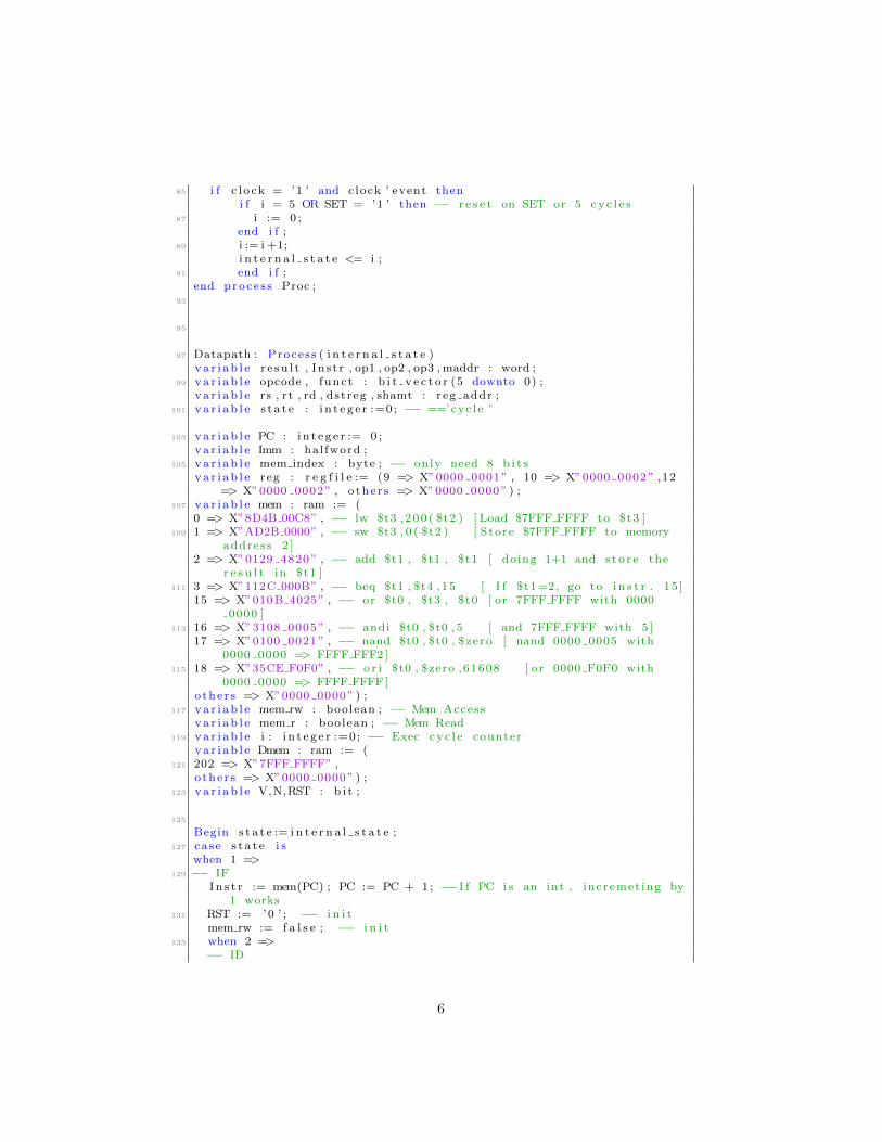
97 Datapath : Process ( i n t e r n a l s t a t e )v a r i a b l e r e s u l t , In s t r , op1 , op2 , op3 , maddr : word ;
99 v a r i a b l e opcode , funct : b i t v e c t o r (5 downto 0) ;v a r i a b l e rs , rt , rd , dstreg , shamt : reg addr ;
101 v a r i a b l e s t a t e : i n t e g e r :=0; −− ==’cyc le ’
103 v a r i a b l e PC : i n t e g e r := 0 ;v a r i a b l e Imm : hal fword ;
105 v a r i a b l e mem index : byte ; −− only need 8 b i t sv a r i a b l e reg : r e g f i l e := (9 => X”0000 0001 ” , 10 => X”0000 0002 ” ,12
=> X”0000 0002 ” , o the r s => X”0000 0000 ” ) ;107 v a r i a b l e mem : ram := (
0 => X”8D4B 00C8” , −− lw $t3 , 2 00 ( $t2 ) [ Load $7FFF FFFF to $t3 ]109 1 => X”AD2B 0000” , −− sw $t3 , 0 ( $t2 ) [ Store $7FFF FFFF to memory
address 2 ]2 => X”0129 4820 ” , −− add $t1 , $t1 , $t1 [ doing 1+1 and s t o r e the
r e s u l t in $t1 ]111 3 => X”112C 000B” , −− beq $t1 , $t4 , 15 [ I f $t1 =2, go to i n s t r . 15 ]
15 => X”010 B 4025” , −− or $t0 , $t3 , $t0 [ or 7FFF FFFF with 00000000 ]
113 16 => X”3108 0005 ” , −− andi $t0 , $t0 , 5 [ and 7FFF FFFF with 5 ]17 => X”0100 0021 ” , −− nand $t0 , $t0 , $zero [ nand 0000 0005 with
0000 0000 => FFFF FFF2 ]115 18 => X”35CE F0F0” , −− o r i $t0 , $zero ,61608 [ or 0000 F0F0 with
0000 0000 => FFFF FFFF ]o the r s => X”0000 0000 ” ) ;
117 v a r i a b l e mem rw : boolean ; −− Mem Accessv a r i a b l e mem r : boolean ; −− Mem Read
119 v a r i a b l e i : i n t e g e r :=0; −− Exec c y c l e counterv a r i a b l e Dmem : ram := (
121 202 => X”7FFF FFFF” ,o the r s => X”0000 0000 ” ) ;
123 v a r i a b l e V,N,RST : b i t ;
125
Begin s t a t e := i n t e r n a l s t a t e ;127 case s t a t e i s
when 1 =>129 −− IF
I n s t r := mem(PC) ; PC := PC + 1 ; −−I f PC i s an int , incremet ing by1 works
131 RST := ’ 0 ’ ; −− i n i tmem rw := f a l s e ; −− i n i t
133 when 2 =>−− ID
6

135 opcode := I n s t r (31 downto 26) ;r s := I n s t r (25 downto 21) ;
137 r t := I n s t r (20 downto 16) ;rd := I n s t r (15 downto 11) ;
139
ds t r eg := r t ;141 Imm := I n s t r (15 downto 0) ;
shamt := I n s t r (10 downto 6) ;143 funct := I n s t r (5 downto 0) ;
op1 := reg ( b i t s 2 i n t ( r s ) ) ; −− a f t e r f i l t e r i n g to an int , s t o r e145 op2 := reg ( b i t s 2 i n t ( r t ) ) ;
op3 := s i g n e x t (Imm) ; −− t h i s i s the immediate va lue a f t e r be ings i gn extended
147
when 3 =>149 −− EX
case opcode i s −− switch on opcode151 when ”100011” => −−lw
a lu add subt ra c t ( ’ 0 ’ , maddr , op1 , op3 ,V,N) ;153 mem rw := true ;
mem r := true ;155 when ”101011” => −−sw
a lu add subt ra c t ( ’ 0 ’ , maddr , op1 , op3 ,V,N) ;157 mem rw := true ;
mem r := f a l s e ;159 when ”000100” => −−beq
a lu add subt ra c t ( ’ 1 ’ , r e s u l t , op1 , op2 ,V,N) ;161 i f r e s u l t = X”0000 0000 ” then−− i f our ALU had a zero output ,
take the branchPC := PC + b i t s 2 i n t ( op3 ) ;
163 RST := ’ 1 ’ ;end i f ;
165 when ”001101” => −−ORIr e s u l t := op1 OR op3 ;
167 when ”001100” => −−ANDIr e s u l t := op1 AND op3 ;
169
when ”000000” => −−0 op code , t h e r e f o r e R type171 ds t r eg := rd ; −−R types always have rd as the dest
case funct i s173 when ”100000” => −−Add
a lu add subt ra c t ( ’ 0 ’ , r e s u l t , op1 , op2 ,V,N) ;175 when ”100001” => −−NAND
r e s u l t :=op1 NAND op2 ;177 when ”100100” => −−AND
r e s u l t := op1 AND op2 ;179 when ”100101” => −−OR
r e s u l t := op1 OR op2 ;181 when othe r s =>
end case ;183 when othe r s =>
end case ;185
when 4 => −−MEM187 i f mem rw = true then −− These f l a g s got s e t above when
decoding lw and swi f mem r = true then −−s e t on read
7
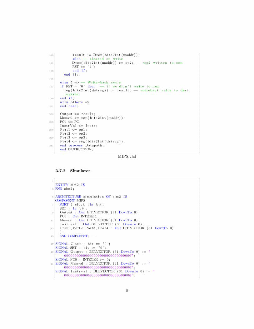
189 r e s u l t := Dmem( b i t s 2 i n t (maddr ) ) ;e l s e −− c l e a r e d on wr i t e
191 Dmem( b i t s 2 i n t (maddr ) ) := op2 ; −− reg2 wr i t t en to memRST := ’ 1 ’ ;
193 end i f ;end i f ;
195
when 5 => −− Write−back c y c l e197 i f RST = ’0 ’ then −− i f we didn ’ t wr i t e to mem
reg ( b i t s 2 i n t ( d s t r eg ) ) := r e s u l t ; −− writeback value to dest .r e g i s t e r
199 end i f ;when othe r s =>
201 end case ;
203 Output <= r e s u l t ;Memval <= mem( b i t s 2 i n t (maddr ) ) ;
205 PC0 <= PC;Ins t rVa l <= I n s t r ;
207 Port1 <= op1 ;Port2 <= op2 ;
209 Port3 <= op3 ;Port4 <= reg ( b i t s 2 i n t ( d s t r eg ) ) ;
211 end proce s s Datapath ;end INSTRUCTION;
MIPS.vhd
3.7.2 Simulator
1
ENTITY sim2 IS3 END sim2 ;
5 ARCHITECTURE s imu la t i on OF sim2 ISCOMPONENT MIPS
7 PORT ( c l o ck : In b i t ;SET : In b i t ;
9 Output : Out BIT VECTOR (31 DownTo 0) ;PC0 : Out INTEGER;
11 Memval : Out BIT VECTOR (31 DownTo 0) ;I n s t r v a l : Out BIT VECTOR (31 DownTo 0) ;
13 Port1 , Port2 , Port3 , Port4 : Out BIT VECTOR (31 DownTo 0)) ;
15 END COMPONENT; −−
17 SIGNAL Clock : b i t := ’ 0 ’ ;SIGNAL SET : b i t := ’ 0 ’ ;
19 SIGNAL Output : BIT VECTOR (31 DownTo 0) := ”00000000000000000000000000000000 ” ;
SIGNAL PC0 : INTEGER := 0 ;21 SIGNAL Memval : BIT VECTOR (31 DownTo 0) := ”
00000000000000000000000000000000 ” ;SIGNAL I n s t r v a l : BIT VECTOR (31 DownTo 0) := ”
00000000000000000000000000000000 ” ;
8
23 SIGNAL Port1 , Port2 , Port3 , Port4 : BIT VECTOR (31 DownTo 0) := ”00000000000000000000000000000000 ” ;
25 −− | | | | | | | | | | | | | | | | | | | | | | | | | | | | | | | | Simulat ion beg ins| | | | | | | | | | | | | | | | | | | | | | | | | | | | | | | | | !
BEGIN27 UUT : MIPS
PORT MAP (29 c l o ck => c lock ,
SET => SET,31 I n s t r v a l => I n s t r v a l ,
Output => Output ,33 PC0 => PC0,
Memval => Memval ,35 Port1 => Port1 ,
Port2 => Port2 ,37 Port3 => Port3 ,
Port4 => Port439 ) ;
PROCESS41 BEGIN
CL : LOOP43 c l o ck <= ’ 0 ’ ;
WAIT FOR 50 ns ;45 c l o ck <= ’ 1 ’ ;
WAIT FOR 50 ns ;47 END LOOP CL;
END PROCESS;49 PROCESS
BEGIN51 WAIT FOR 5000 ns ;
END PROCESS;53
55 END s imu la t i on ;
simulator.vhd
References
[1] David A. Patterson, John L. Hennesy, Computer Organization and Design.Morgan Kaufmann, Massachusetts, 4th Revised Edition, 2012.
[2] Peter J. Ashden, VHDL Tutorial. Elsevier Science, USA, 2004
9
PC
Instr
uctio
n
Me
mo
ryR
eg
iste
r
File
AL
U
Da
ta
Me
mo
ry
AL
U
AL
U
Re
g 1
Se
lect
Re
g 2
Se
lect
Inst[
25
-21
] Inst[
20
-16
]
Co
ntr
ol
M U X
Write
Se
lect
Inst[
15
-11
]
Write
Da
ta
Re
g 1
Da
ta
Re
g 2
Da
ta
M U XS
ign
Exte
nd
Inst[
15
-0]
4
M U X
<<
2
Ad
dr
Re
ad
Write
M U X
Re
gD
st
A L U S r c
AN
D
Ze
ro
Ou
tpu
t
B r a n c h
Me
mT
oR
eg
AL
U
Co
ntr
ol
AL
UO
p
Me
mW
rite
Re
gW
rite
Figure 1: Block Diagram
10
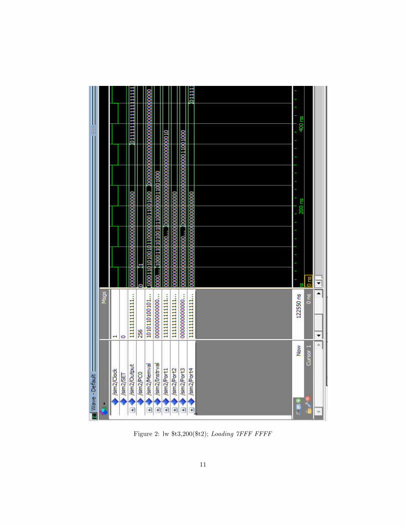
Figure 2: lw $t3,200($t2); Loading 7FFF FFFF
11
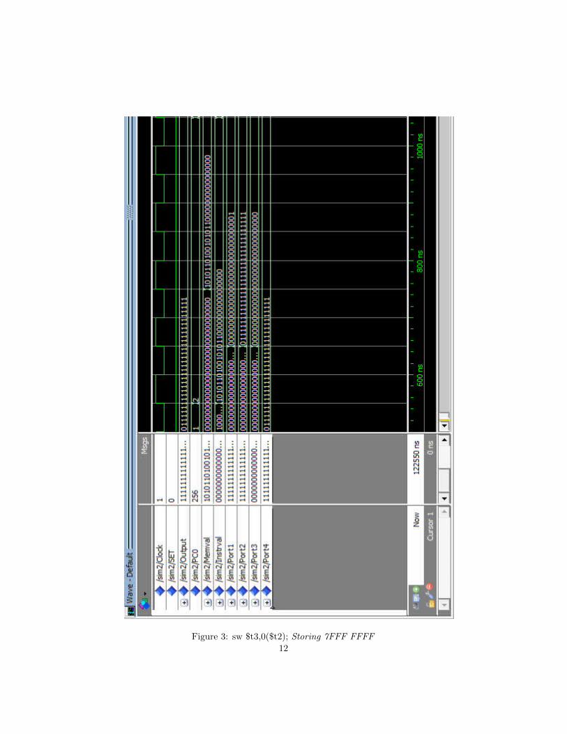
Figure 3: sw $t3,0($t2); Storing 7FFF FFFF
12
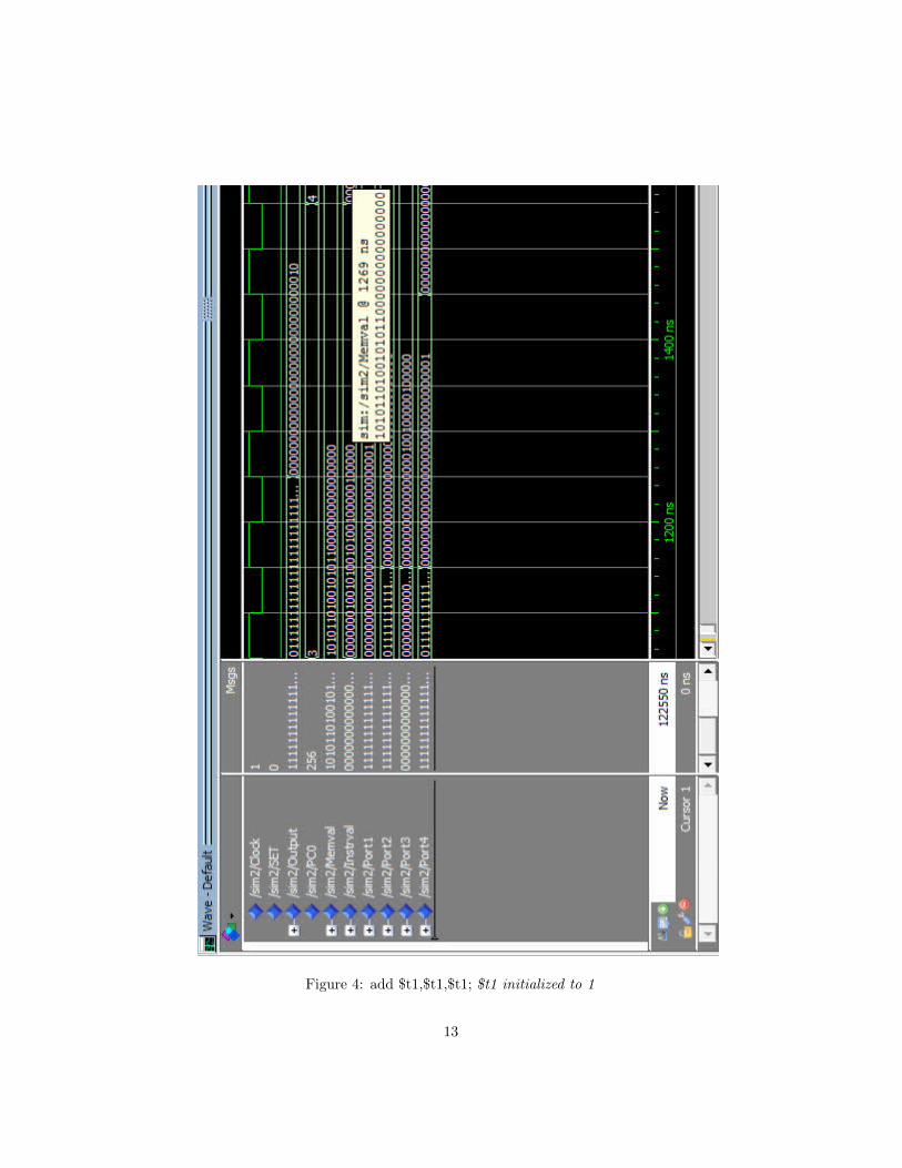
Figure 4: add $t1,$t1,$t1; $t1 initialized to 1
13
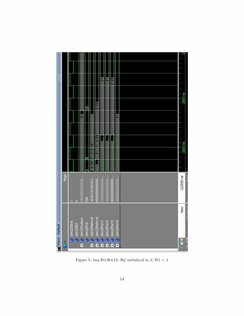
Figure 5: beq $t1,$t4,15; $t4 initialized to 2, $t1 = 2
14
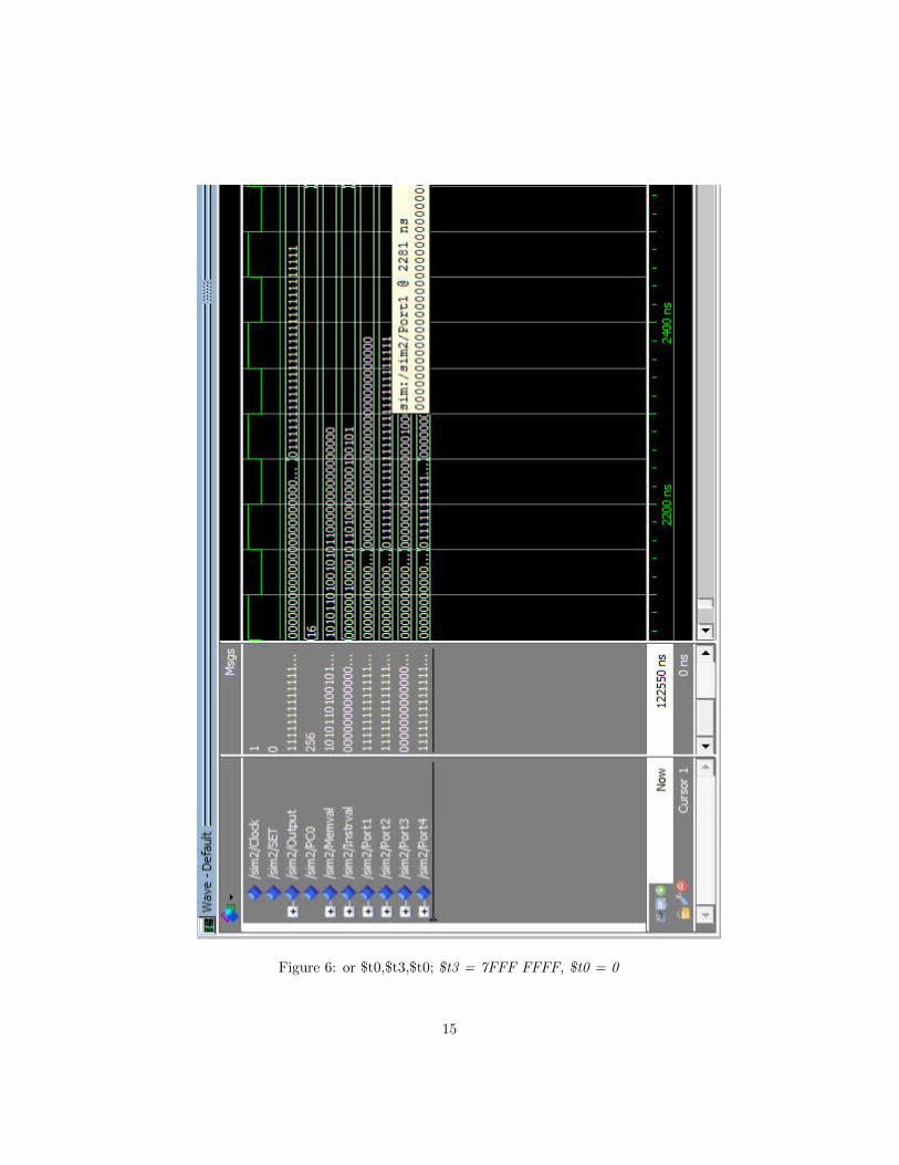
Figure 6: or $t0,$t3,$t0; $t3 = 7FFF FFFF, $t0 = 0
15
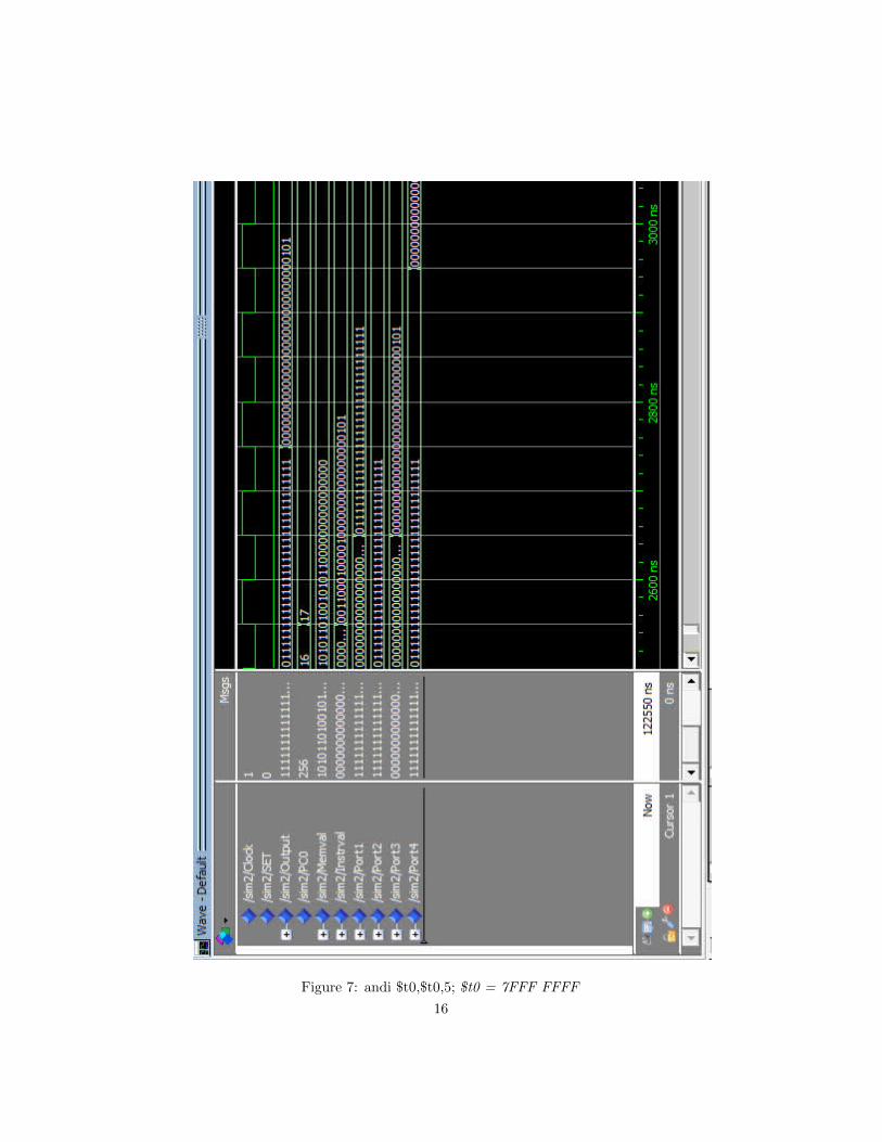
Figure 7: andi $t0,$t0,5; $t0 = 7FFF FFFF
16
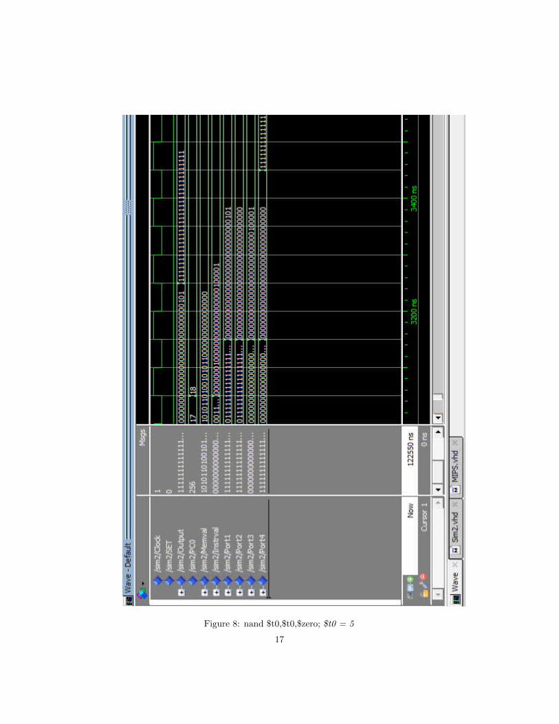
Figure 8: nand $t0,$t0,$zero; $t0 = 5
17
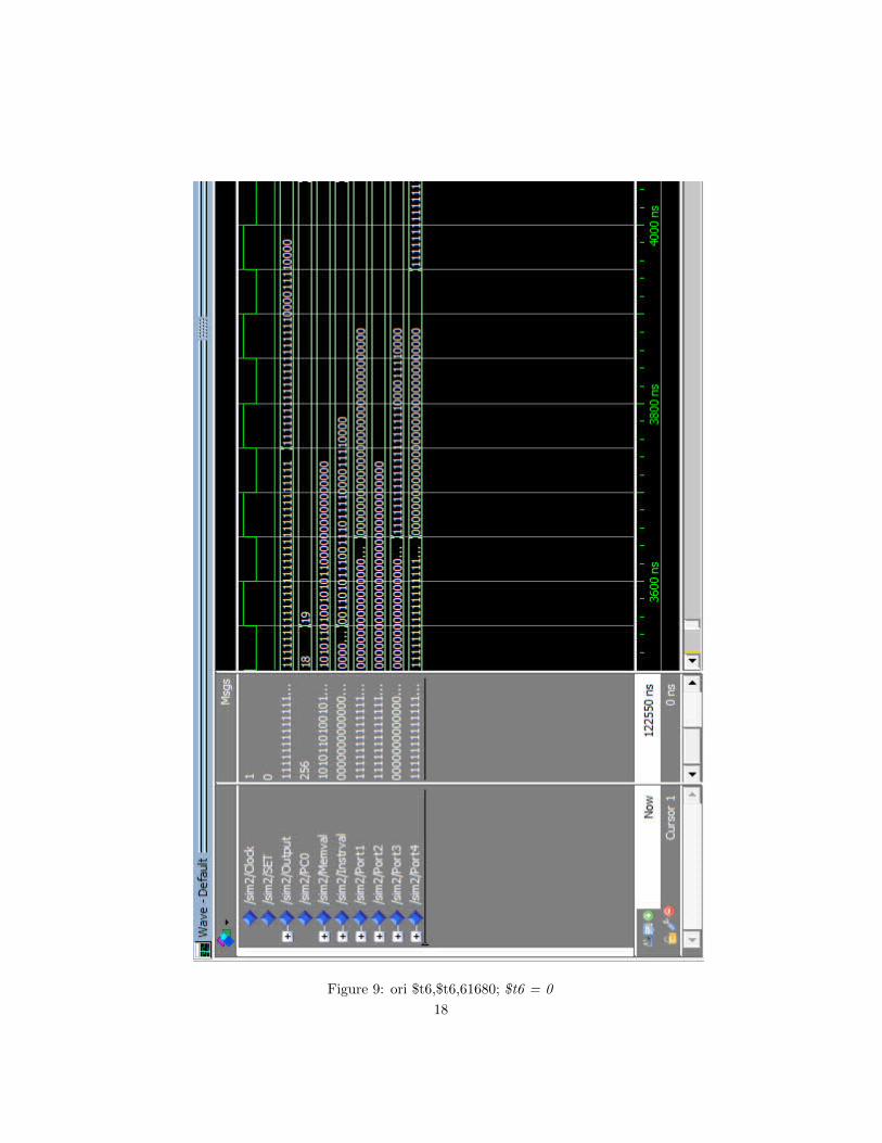
Figure 9: ori $t6,$t6,61680; $t6 = 0
18