Embed Size (px)
Citation preview
Methodology for the Formal Specification of RTL RISC Processor Designs
(With Particular Reference to the ARM6)
by
Daniel Paul Schostak
Submitted in accordance with the requirements
for the degree of Doctor of Philosophy.
The University of Leeds
School of Computing
October 2003
The candidate confirms that the work submitted is his own and
that the appropriate credit has been given where reference
has been made to the work of others. This copy has been supplied on
the understanding that it is copyright material and that no quotation from
the thesis may be published without proper acknowledgement.
i
Acknowledgements The research described in this thesis was carried out as part of an EPSRC funded project
on the formal specification and formal verification of the ARM6. This project involved
collaboration between a team at the University of Leeds to formally specify the ARM6
and a team at the University of Cambridge to formally verify the ARM6. The team at
the University of Leeds has included Prof. Graham Birtwistle, Dr. Keith Hobley, Robin
Hotchkiss, Dominic Pajak and Daniel Schostak; that at the University of Cambridge
has included Anthony Fox and Prof. Mike Gordon.
Thanks are expressed for the assistance members of both teams provided in relation to
this project. In particular, the author would like to thank Graham Birtwistle for
bringing this project to the attention of the author. Also ARM Ltd. must be thanked for
making available documents relating to the design of the ARM6 and the other support
the company provided during this project. Lastly, the author would like to thank
Matthew Hubbard for acting as supervisor during the final preparation of this thesis.
The contribution of the author to this project was the development of a methodology for
the formal specification of RTL RISC processor core designs and the application of
this methodology to the design of the ARM6. In addition, the author provided support
to help other members of the teams to understand the details of the design of the ARM6.
ARM is a registered trademark of ARM Limited.
MIPS and R2000 are registered trademarks of MIPS Technologies, Incorporated.
ii
Abstract Due to the need to meet increasingly challenging objectives of increasing performance,
reducing power consumption and reducing size, synchronous processor core designs
have been increasing significantly in complexity for some time now. This applies to
even those designs originally based on the RISC principle of reducing complexity in
order to improve instruction throughput and the performance of the design.
As designs increase in complexity, the difficulty of describing what the design does,
and demonstrating the design does indeed do this, also increases. The usual practice of
describing designs using natural languages rather than formal languages exacerbates this
because of the ambiguities inherent in natural language descriptions. Hence this thesis
is concerned with the development of a scalable methodology for the creation of
formal descriptions of synchronous processor core designs.
Not only does the methodology of this thesis provide a standardised approach for
describing synchronous processor core designs, but the descriptions that it generates
can be used as a basis for the formal verification of the design; and thus facilitate
solutions to the problems that increasing complexity poses for traditional validation.
The concept of different presentations of one description is part of the methodology of
this thesis and is used to reconcile differences in how the description is best used for
one purpose or another.
The methodology of this thesis was developed for the formal specification of the ARM6
processor core and thus this design provides the primary example used in this thesis.
Case studies of the use of the methodology of this thesis with other processor cores and
a modernised version of the ARM6 are also discussed.
iii
Table of Contents
Acknowledgements ............................................................................................................ i
Abstract ............................................................................................................................. ii
1 Introduction................................................................................................................ 1
1.1 Specification and Design .................................................................................... 2
1.2 Specification and Synthesis ................................................................................ 3
1.3 Specification and Simulation .............................................................................. 4
1.4 Specification and Verification ............................................................................ 6
1.5 Related Research................................................................................................. 9
1.6 Outline of this Thesis ........................................................................................ 12
1.7 Contributions of this Thesis .............................................................................. 13
2 Methodology ............................................................................................................ 15
2.1 Aims.................................................................................................................. 15
2.2 Basis .................................................................................................................. 16
2.2.1 Hierarchical Representation....................................................................... 16
2.2.2 Definition of Terms ................................................................................... 17
2.2.3 Use in Formal Verification ........................................................................ 19
2.2.4 Relation to Aims ........................................................................................ 23
2.3 Method .............................................................................................................. 24
2.3.1 Mathematical ............................................................................................. 24
2.3.2 Engineering................................................................................................ 48
2.3.3 Executable.................................................................................................. 52
2.4 Comparison of Presentations ............................................................................ 70
2.5 Summary ........................................................................................................... 72
3 Overview of the ARM6............................................................................................ 73
3.1 Outline of Informal Programmer’s Model Specification.................................. 73
3.1.1 Operating Modes........................................................................................ 73
3.1.2 Exceptions.................................................................................................. 74
3.1.3 Register Banks ........................................................................................... 75
3.1.4 Instruction Set ............................................................................................ 75
3.1.5 Instruction Set Encoding............................................................................ 77
3.2 Outline of Informal Hardware Implementation Specification .......................... 79
iv
3.2.1 Signal Description...................................................................................... 79
3.2.2 Coprocessors.............................................................................................. 81
3.2.3 Datapath of Processor Core ....................................................................... 82
3.2.4 Control Subsystem of Processor Core ....................................................... 84
3.3 Summary ........................................................................................................... 88
4 Specifying the ARM6 .............................................................................................. 89
4.1 General Principles............................................................................................. 89
4.2 Mathematical Presentation................................................................................ 95
4.3 Engineering Presentation .................................................................................. 99
4.4 Executable Presentation .................................................................................. 100
4.5 Summary ......................................................................................................... 106
5 Overview of the Modernised ARM6 ..................................................................... 107
5.1 Modernising the ARM6 .................................................................................. 107
5.2 Outline of Informal Programmer’s Model Specification................................ 110
5.3 Outline of Informal Hardware Implementation Specification ........................ 111
5.3.1 Signal Description.................................................................................... 111
5.3.2 Coprocessors............................................................................................ 112
5.3.3 Datapath of Processor Core ..................................................................... 112
5.3.4 Control Subsystem of Processor Core ..................................................... 114
5.4 Summary ......................................................................................................... 119
6 Specifying a Modernised ARM6 ........................................................................... 120
6.1 General Principles........................................................................................... 120
6.2 Mathematical Presentation.............................................................................. 127
6.3 Engineering Presentation ................................................................................ 132
6.4 Executable Presentation .................................................................................. 132
6.5 Summary ......................................................................................................... 137
7 Further Applications .............................................................................................. 138
7.1 Motivation for Selection of Chosen Processor Cores ..................................... 138
7.2 Overview of the DLX ..................................................................................... 139
7.2.1 Outline of Informal Programmer’s Model Specification......................... 139
7.2.2 Outline of Informal Hardware Implementation Specification ................. 141
7.3 Specifying the DLX ........................................................................................ 146
7.4 Overview of the Simplified MIPS R2000....................................................... 148
v
7.4.1 Outline of Informal Programmer’s Model Specification......................... 148
7.4.2 Outline of Informal Hardware Implementation Specification ................. 152
7.5 Specifying the Simplified MIPS R2000 ......................................................... 157
7.6 Summary ......................................................................................................... 160
8 Conclusions............................................................................................................ 161
Bibliography.................................................................................................................. 163
Appendix A: DLX Formal Specification—Mathematical Presentation ....................... 165
A.1 Datapath Specification .................................................................................... 165
A.2 Datapath Control Specification....................................................................... 171
A.3 Pipeline Control Specification ........................................................................ 186
Appendix B: DLX Formal Specification—Engineering Presentation .......................... 191
B.1 Datapath Specification .................................................................................... 191
B.2 Datapath Control Specification....................................................................... 191
B.3 Pipeline Control Specification ........................................................................ 199
Appendix C: General Simulator—Reusable Modules in Executable Presentation ...... 201
C.1 common.sml.................................................................................................... 201
C.2 inputs.sml ........................................................................................................ 226
C.3 buses.sml......................................................................................................... 228
C.4 latches.sml....................................................................................................... 244
C.5 outputs.sml ...................................................................................................... 250
C.6 signals.sml....................................................................................................... 252
C.7 state.sml .......................................................................................................... 256
C.8 coordinator.sml ............................................................................................... 279
vi
List of Tables and Figures Figure 2-1: Example Intermediate Specifications in Formal Verification......................20
Figure 2-2: Example Formal Verification Hierarchy......................................................21
Figure 2-3: Three Stage Instruction Pipelining...............................................................26
Figure 2-4: Five Stage Instruction Pipelining .................................................................27
Table 2-1: Life Cycle of an Instruction in Three Stage Instruction Pipeline ..................29
Table 2-2: Life Cycle of an Instruction in Five Stage Instruction Pipeline ....................30
Table 2-3: Syntax for Transfers between the Entities in a Specification........................35
Figure 2-5: Resolving Discontinuities in Bits an Entity is Defined Over.......................36
Table 2-4: Syntaxes for Expressing Forms of Combinational Logic..............................38
Figure 2-6: Example of Mathematical Presentation of Datapath Specification..............39
Table 2-5: Summary of Timing Annotations for Specification of the ARM6................41
Figure 2-7: Layout of Mathematical Presentation of Datapath Control Specification ...47
Figure 2-8: Example of Engineering Presentation of Datapath Control Specification...49
Table 2-6: Summary of Reusable Modules of Executable Presentation.........................54
Table 2-7: Summary of Modules Particular to Each Executable Presentation ...............59
Figure 2-9: Interaction of Modules of an Executable Presentation.................................60
Figure 2-10: Example *_LOGIC Function of functions_datapath_*.sml Module .........64
Figure 2-11: Example datapath_specification Function of Datapath.sml Module .........65
Figure 2-12: Partial Waveform Trace Created by Simulating the Original ARM6........68
Figure 2-13: Partial Behavioural Trace Created by Simulating the Original ARM6 .....68
Table 3-1: ARM6 Operating Modes ...............................................................................73
Figure 3-1: ARM6 Program Status Register ...................................................................75
Figure 3-2: ARM6 Instruction Set Encoding ..................................................................77
Table 3-2: Types of ARM6 Bus Transfer .......................................................................80
Table 3-3: Coprocessor Response Types for the ARM6 ................................................81
Figure 3-3: ARM6 Processor Core Datapath ..................................................................83
Table 3-4: Key to Datapath Diagram..............................................................................84
Figure 3-4: Dataflow of ARM6 Control Blocks .............................................................86
Figure 4-1: Instruction Steps Used to Specify the Original ARM6................................94
Table 4-1: Summary of Modules Used for the Simulation of ARM6 Coprocessors ....103
Figure 5-1: Modernised ARM6 Instruction Set Encoding............................................110
Table 5-1: Types of Modernised ARM6 Bus Transfer .................................................111
Table 5-2: Equivalents of Modernised ARM6 Memory Signals ..................................112
Figure 5-2: Modernised ARM6 Processor Core Datapath............................................113
vii
Table 5-3: Data Hazards of Modernised ARM6...........................................................117
Table 5-4: Structural Hazards of the Modernised ARM6.............................................118
Figure 6-1: Instruction Steps Used to Specify the Modernised ARM6 ........................126
Figure 7-1: DLX Instruction Set Encoding...................................................................140
Figure 7-2: DLX Processor Core Datapath...................................................................142
Table 7-1: Data Hazards of DLX..................................................................................146
Figure 7-3: MIPS R2000 Instruction Set Encoding ......................................................150
Table 7-2: Unified Bus Equivalents of MIPS R2000 Memory Signals ........................152
Table 7-3: Timing of Signals for MIPS R2000 Memory Accesses ..............................153
Figure 7-4: MIPS R2000 Processor Core Datapath ......................................................154
Table 7-4: Data Hazards of MIPS R2000 .....................................................................157
1
1 Introduction Specification is an important part of the process of successfully developing a product;
since without it, how well the nature of the product can be defined cannot be assessed
and nor can continuity within the development process. Depending on the complexity of
the product, specifications may be required at different levels of abstraction:
1. The development of all but the most trivial of products will benefit from a statement
in general terms of what the product can be used for and in what circumstances;
without defining how these criteria should be met. Specifications of such generality
are valuable in providing an overview of the product and hence are best expressed in
a natural language instead of a language created to be mathematically representable
(a defining feature of formal specifications). For instance, at this level of abstraction
the ARM6 processor core may be specified as a processor core that supports
execution of instructions defined by the ARM Instruction Set Architecture version 3
(see Seal and Jaggar 2000) using a 32-bit address space. The operating conditions
under which the ARM6 processor core may be used are no different from those of
most general-purpose processor cores, so these do not need to be explicitly specified.
2. Specifications at the preceding level of abstraction will be too generalised to provide
an adequate description of the functionality of even moderately complex products.
Hence another specification is needed that presents what the product can do in detail;
but does so with an appropriate structure, so the specification is still readable despite
added detail. Returning to the example of the ARM6 processor core, specification of
the ARM Instruction Set Architecture version 3 itself would be required, as well as
specification of performance objectives (such as power consumption, size and speed)
and the interfaces used to connect the ARM6 processor core and other devices.
(Note the level of abstraction of these three features requiring specification is similar
insofar as details of how the ARM6 processor core should meet the specification
should be omitted and is dissimilar in terms of its specificity to an implementation of
the ARM6 processor core—see discussion of Programmer’s Model specification in
section 2.2.2.) While informal specifications, such as that of Seal and Jaggar (2000)
for the Instruction Set Architecture specification, are used at this level of abstraction,
sufficient detail is involved that use of formal specifications can be advantageous
(see discussion in following sections).
3. Specifications at both the preceding levels of abstraction only define what products
can do, but not how any of what can be done, should be done. In simple instances,
2
how it should be done may be apparent from what can be done, but for products of
moderate complexity, this is unlikely to be so in every instance. Thus specification at
another less general level of abstraction is needed to indicate how the functionality of
the product is achieved. Continuing with the example of the ARM6 processor core,
this is the level of abstraction of the Hardware Implementation specification.
Although the formal specification developed using the methodology of this thesis for
the ARM6 processor core was based on the informal ARM2x Block Specifications,
the formal specification resolves several points found to be not wholly unambiguous
in the original. Hence, the detail involved in specifications at this level of abstraction
is sufficient for the use of formal specifications to be advantageous.
The methodology of this thesis is concerned with developing formal specifications at
the third level of abstraction listed. Consideration of the relevance of such specifications
to the process of developing a processor core in certain key areas follows. (Note that
section 2.2 provides further definition of the terms Instruction Set Architecture and
Hardware Implementation as used by the methodology of this thesis.)
1.1 Specification and Design
The design may be developed before the Hardware Implementation specification itself,
from specifications at higher levels of abstraction. However, the translation process
required to construct the design according to such specifications involves the details that
the Hardware Implementation specification should include. Therefore separating
development of the design and the Hardware Implementation specification may involve
duplication of work. Similarly, using informal Hardware Implementation specifications,
instead of formal Hardware Implementation specifications while developing the design,
and then creating the latter from the former, may involve further duplication of work.
Indeed, the use of a natural language by informal specifications often introduces
unintended ambiguities, which must be resolved equally for the success of the design
and for the development of a formal specification.
Consequently it might be argued an explicit Hardware Implementation specification
serves to document necessary work, such that creating the former before beginning on
the design does not need to involve significantly more work than just treating the design
as the Hardware Implementation specification. Since the approach required to create
formal specifications reflects the desired behaviour of designs—complete, predictable
3
and unambiguous—better than the approach required to create informal specifications,
using the former may uncover or avoid problems in the design that the latter does not.
For example, Sawada (1999) pp. 168-169 reports finding a number of design faults with
the FM9801 processor core just by creating a formal specification of it, even after using
functional simulation to perform an initial verification. However informal specifications
are still more commonly used than formal specifications, because the latter often require
a background in mathematics and/or logic that most engineers who design and/or verify
processor cores lack. Thus, one of the aims of the methodology developed for this thesis
is its accessibility to engineers regardless of such background (see section 2.1).
1.2 Specification and Synthesis
Traditionally, processor cores were designed at a level of abstraction sufficient for
fabrication of the finished product direct from the design. Now it is common to design
at a level of abstraction that offers greater flexibility to make minor modifications
without further changes to the design becoming necessary, greater scalability to handle
increasing complexity and greater independence from the technology used to fabricate
the finished product. The process of transforming a design from this level of abstraction,
to one that may be used in the fabrication of the finished product, is termed synthesis;
and usually involves mapping a Register Transfer Level (RTL) representation to one
consisting only of logic gates. (Registers are entities used to store intermediate results,
thus a RTL representation specifies the intermediate results a design stores, as well as
where it stores the intermediate results, and how the intermediate results flow through
the design.)
The logic gate representation synthesised from a RTL representation usually requires
further transformations such as place and route (which finalises component layout and
component interconnections) before it can be used to fabricate the finished product.
While functional simulation can be used to ensure that the logic gate representation
before and after such transformations behaves identically for appropriate test vectors,
functional simulation of logic gates is much more computationally intensive than RTL.
Therefore, methodologies using equivalence checkers have been developed to minimise
the extent of functional simulation of logic gates required—see, for example, Chander
and Vaideeswaran (2001). Such tools can be used to prove the functional equivalence of
two versions of a logic gate representation of a design, a RTL representation of a design
and a logic gate representation of a design, or two versions of a RTL representation of
4
a design (although not all tools support each of these different proof tasks equally well).
The availability of such tools allows this thesis to focus on RTL designs without
reducing the rigour that formal specification introduces, because equivalence checkers
may be used to propagate this to representations at lower levels of abstraction.
Research such as that of Blumenröhr and Eisenbiegler (1997) on using theorem provers
to construct synthesis tools, and not the more usual informal programming techniques,
shows how synthesis may become a formal method rather than a process that requires
the application of formal methods. Currently, formally constructed synthesis tools
cannot match the extent to which informally constructed synthesis tools can optimise
the resultant logic gate representations. Yet, should this change, formal specifications
could become much more important in the synthesis process since these would provide
the natural starting point for the tools that perform formal synthesis.
Another area of research with implications for the methodology of formal specification
developed for this thesis is that of synthesis from algorithmic descriptions rather than
RTL specifications. For example, Heath and Durbha (2001) document how a version of
the MIPS R2000 processor core was synthesised from a purely algorithmic description
and a prototype of the finished product created. Again, the issue preventing adoption of
this technique of synthesis is that the standard methods are much better at optimising
the resultant logic gate representations. If synthesis from algorithmic descriptions
became accepted, the level of representation at which it is appropriate to construct
formal specifications would change from the RTL level to the algorithmic level.
1.3 Specification and Simulation
The use of functional simulation to model the behaviour of a design under stimulus,
using algorithms to approximate the behaviour that the design would have, if fabricated,
is standard practice. Hence, it is used for various purposes that would otherwise require
the much more expensive and labour intensive option of creating an actual prototype of
the finished product. For example, functional simulation is used to perform verification
(see section 1.4), to observe the behaviour of a design as it is developed (rather than
waiting for the entire design to be completed), to evaluate how modifications to a design
affect its behaviour, and so on.
5
Accuracy of simulation tools is limited by the extent to which physical characteristics
are simplified, such as by treating the value of a signal as discrete instead of continuous,
but in most cases, this is not a problem since these simplifications reflect assumptions in
the method used to create the design itself. However, serious problems with accuracy
may arise because simulation tools only model a description of a design and thus rely on
the correspondence of a description and the finished product it is being used to model.
Finding such problems using just simulation tools would be difficult as it would involve
examining all the output to determine whether it matches what would be predicted by
the specification and even then this depends on having supplied the correct stimulus for
incorrect output to be elicited. Yet if the description used for simulation is derived from
a formal specification using a provably correct algorithm, or is a formal specification,
the problem is reduced to whether the specification is correct. (As noted in section 1.2,
confidence in the correspondence between descriptions at the RTL level of abstraction,
which is the level at which most functional simulation is done when creating a design
rather than evaluating possibilities for a design, may be obtained by using tools such as
equivalence checkers.)
Executable specifications can be used directly for functional simulation and thus have
the advantages discussed above over those specifications that cannot be used directly for
functional simulation. Furthermore, executable specifications allow the output from
simulation tools to be compared to the desired output as inferred from a specification at
a higher level of abstraction (which because it is simpler is more likely to be correct).
This can be useful in finding problems with the executable specification; for example,
Anderson and Shaw (1997; pp. 57-58) report discovering three bugs in this fashion;
one of which might otherwise not have been discovered until a prototype was created,
when it would have been more difficult to fix. Conversely with complex specifications,
if the result of some interaction between different entities is not clear from an inspection
of the specification, the behaviour exhibited may be observed directly by applying
appropriate stimulus in functional simulation.
The speed at which simulation tools can model the behaviour of a design is important:
the greater the speed, the greater the use that can be made of the simulation tool before
time constraints require the first prototype, and/or the first revision, to be constructed.
For this reason, most simulation tools are written in informal programming languages
and particularly those, such as C or C++, regarded as facilitating the development of
6
fast programs. However, by using appropriate methodologies, like the one outlined by
Wilding et al (2001), programs may be developed using formal programming languages
without compromising on speed or on provability. As indicated by Wilding et al (2001),
to achieve ninety percent of the speed of C programs, some of the functional aspects of
primitive types like arrays may have to be discarded; but if the interface is not altered,
proofs can be constructed to ensure this is harmless. Consequently, the creation of
executable specifications is one of the aims of the methodology developed for this thesis
(see section 2.1).
1.4 Specification and Verification
Verification that should be performed on any design may be categorised as follows:
1. CORRECTNESS: does the design fulfil all of the functions it was intended to?
2. PERFORMANCE: does the design use more power than it should, function inefficiently
or otherwise fail to meet operational objectives? (The size or area of the design
should also be included in this category.)
3. QUALITY: were physical faults introduced into the design by the fabrication process?
Each of these categories has its role in assuring the usability of the finished product that
results from a design. However, the first is arguably more fundamental than the others,
and it is this category that is pertinent for the specifications that may be created using
the methodology developed for this thesis.
Bergeron (2000) discusses the following methods used for verifying the correctness of
commercial designs:
• CODE REVIEWS: require each significant part of a design to be inspected by someone
other than the person who created that part for any errors missed during its creation.
• FUNCTIONAL SIMULATION: used as described in section 1.3 to model the behaviour of
a design such that the predicted output can be compare to the desired output.
• CODE COVERAGE: an add-on to functional simulation that provides an indication of
how well the different parts of a design may have been exercised by various stimuli.
• LINTING TOOLS: perform static analysis on the description of a design to identify
possible instances of common errors made when writing such descriptions.

7
• MODEL CHECKING: attempts to prove particular properties of a design using logic;
either propositions that should always be true or ones that should always be false.
Code coverage, if supplemented by knowledge about a design, may indicate errors by
demonstrating that some part of a design is not exercised even when the correct stimuli
are supplied to a design. However, it is primarily used to quantify the quality of
functional simulation, and not to find errors directly, as code reviews are likely to find
these kinds of errors, and others besides, without requiring significant amounts of
functional simulation. While limited analysis of the functionality of a design is involved
in code coverage, linting tools involve no such analysis. Hence, the utility of such tools
for finding errors is also limited, because only probable errors, instead of definite errors,
can be identified using linting tools.
For all but the simplest designs, to use functional simulation to test that the modelled
and the desired output of a design are identical for all stimuli would be unfeasible due to
the required computation time. Hence, usually only the important properties are tested
using stimuli carefully chosen to give the best possibility of finding errors in the design.
For example, though all instructions in the ARM Instruction Set Architecture version 3
are conditionally executed (see section 3.1), the task of testing the correctness of this for
a processor core designed to implement this Instruction Set Architecture can be reduced
to testing whether condition codes are evaluated correctly using functional simulation of
an assembly language routine that:
1. Sets the Current Program Status Register’s status flags to one of 16 possible values.
2. For one of the fifteen possible condition codes execute a branch to a failure routine
or to next part of the test depending on whether branch should fail to execute or not.
3. Repeat 2 for each of the fifteen possible condition codes.
4. Repeat 1 2 3 for each of the sixteen possible values of the status flags.
Each complete set of stimuli (such as that provided by the code required to implement
steps 1 and 2 in the above example) is called a test vector, and a set of several of these
(such as that provided by the code needed to implement steps 3 and 4) may be required
to test just one property.
8
The methods of verification considered so far attempt to find the errors in a design,
rather than demonstrate that the design is correct, but model checking as a method of
formal verification attempts to prove the correctness of a design. Still it is not applied to
a design as a whole, but to individual properties of that design, and thus it only assures
the correctness of the aspects of the design associated with those properties.
Furthermore, the computation time that model checkers may require to prove properties
on a design, or a part of a design, increases with the complexity of that design or part.
Theorem provers are another type of tool that can be used for formal verification and,
unlike model checkers, can be used to prove the correctness of a design as a whole.
Such tools work by demonstrating that one specification follows from another
(for example that a specification at the second level of abstraction listed in section 1.1,
follows from one at the third) and thus in contrast to the previous methods require
explicit formal specifications before application is possible. (Although the properties
used by model checkers must be expressed in a mathematically representable language,
the specification of the design as a whole can be left implicit.) However, as discussed in
previous sections creating a specification before a design, or creating the specification
as the design itself is created, often results in better productivity than creating the design
from an implicit specification. Consequently, the requirement for explicit specifications
is not necessarily a disadvantage, and if a formal specification is developed alongside
the design, rather than after or before, neither the design nor the verification processes
are delayed.
The use of theorem provers is less straightforward than use of any of the other methods
discussed before, due to the extent of the contributions and interventions required from
the user; which increases with the complexity of the design to which theorem provers
are applied. Moreover, while the previous methods can be used with a background
similar to that required for the design of processor cores, with some minor additions,
use of theorem provers requires an additional specialist background. These are two of
the main reasons preventing the adoption of theorem provers as the tools of choice for
verification of processor cores in industry. Nevertheless, as reported by Kam et al
(2000; p. 1501), methods of verification that cannot be used to prove the correctness of
a design as a whole require an unsustainable growth in computation to achieve
reasonable levels of confidence in the correctness of designs as complexity increases.
Indeed, the rate at which the computation required is growing is actually greater than
9
the rate at which the capability for computation is growing. Therefore one of the aims of
the methodology developed for this thesis is that the formal specifications it can be used
to create should be suitable for use with formal verification in general (see section 2.1)
and theorem provers in particular (see section 2.2.3).
1.5 Related Research
Although, as discussed above, a formal specification of a processor core design may be
useful for more than just formal verification, most research on applying formal methods
to processor core designs assumes this is its primary purpose. Hence related research on
formal verification of processor core designs is discussed with reference to the approach
to formal specification that it uses.
Not surprisingly, the focus of research has changed over time to reflect as far as possible
the state of the art in the design of processor cores. Hence initially research concerned
processor cores with no pipelining such as the Viper (Cohn 1988), microcoded control
such as the AAMP5 (Srivas and Miller 1996) or both like the FM8501 (Hunt 1994).
These early processor cores differ substantially from the ARM6, which is pipelined and
has hardwired control, and it is not one of the aims of the methodology developed for
this thesis to be able to specify these processor cores (see section 2.1) since the tactics
required might be quite different. Thus, the selection of research discussed here is later
and concerned with processor cores that, like the ARM6, may be described as RISC.
The latest research often considers additional features such as out-of-order execution
(for example, Kristic et al 1999), which some recent commercial processor core designs
(such as the PowerPC 620) have included. However, as briefly discussed in section 5.1,
the work required to add these features to the ARM6 processor core (the main focus of
this thesis) and then alter the methodology of this thesis to specify the resultant design
would be significant. Therefore, these features are not considered in detail in this thesis
and thus research that focuses on such features is not discussed here.
Burch and Dill (1994) decompose their specification of an implementation of the DLX
according to the items of state that an assembly language programmer may reference,
such as the instruction memory and the register file. A formula, using a simple syntax of
if then else expressions, Boolean values, Boolean operators and uninterpreted functions,
is constructed for each item of state and specifies how its current value is mapped onto
its next value with reference to ‘pipe registers’, which maintain intermediate results
10
between mappings and ensure that the formal specification is clock cycle accurate.
Since the behavioural features of the implementation are specified independently of
the implementation itself and combinational logic that calculates a result, rather than
just selects one of several possible results, is specified only by uninterpreted functions,
the resultant formal specification is quite abstract. This could be advantageous for
configurable implementations because the formal specification may well abstract over
individual configurations. Conversely, the formal specification and the implementation
differ sufficiently in abstraction that errors may be masked or that some features such as
an instruction that has different execution times according to the data it is executed on
may be very difficult to represent.
Although Windley (1995) describes his generic interpreter theory in terms of specifying
a non-pipelined processor core (AVM-1) created for the purposes of formal verification,
Coe (1994) used this theory to create a formal specification of the SAWTOOTH
processor core, which is a pipelined design. The formal specification is written using
constructs developed in the HOL theorem prover instead of a syntax created especially
for formal specification of processor cores and consists of three levels of interpreters.
In general, the formal specification is intended to reflect the VHDL implementation,
such that the least abstract interpreter (the Electronic Block Model) is decomposed into
functions corresponding to components in this implementation. The Phase interpreter
rewrites these functions such that the definition of each is incorporated into functions
that completely specify the behaviour of the processor core for particular clock phases
as appropriate. The most abstract interpreter, the Pipeline interpreter describes how
these clock phase functions should be combined to specify the behaviour exhibited in
one clock cycle. These three interpreters accurately represent the implementation of
the SAWTOOTH processor core; but not without some significant duplication of effort,
even though no single interpreter itself provides a complete formal specification.
Tahar and Kumar (1998) also wrote their formal specification of an implementation of
the DLX processor core in the HOL theorem prover and similarly used three interpreters
to decompose the formal specification. Although the Electronic Block Model interpreter
is less behavioural than that of Coe (1994), and Stage interpreter is used instead of
Pipeline interpreter, the main difference in the approach of these formal specifications
concerns the use Tahar and Kumar make of instruction classes. The function definitions
for the Phase interpreter and the Stage interpreter are distinguished by instruction class
11
(and in the case of the Phase specification by clock phase as before), which facilitates
understanding of how the DLX may be used by the assembly language programmer
from the formal specification of its implementation. However, the formal specification
is not itself executable and as presented does not readily allow for the specification of
instruction classes that require iteration or other complex behaviours.
Formal specifications have been written directly using other formal provers than HOL.
For example, Sawada (1999) used the ACL2 theorem prover for formal specification of
the implementation of the FM9801 processor core. This formal specification specifies
the next state of the processor core in terms of functions that specify the next state of
significant blocks in the design, which in turn are specified in terms of functions that
specify the next state of the components that comprise these blocks. The decomposition
is continued until components are being described in terms of simple logical operations
on standard state components such as register files and latches. Although this provides
an accurate representation of the full implementation of the FM9801 processor core,
how the processor core is used by the assembly language programmer is obscured by
decomposing the formal specification according to the structure of the implementation.
In addition, ACL2 is based on the LISP programming language, which in its treatment
of programs as lists is quite different to the programming languages that will be familiar
to most hardware engineers. (The ML programming language, on which HOL is based,
is more conventional in its treatment of programs as collections of functions.)
All the approaches considered so far attempt to create formal specifications to represent
the design directly, albeit at somewhat different levels of abstraction. Other approaches
have attempted to substitute simpler designs for actual implementations such that
formal specifications may be created for the former rather than the latter. For example,
Levitt and Olukotun (1997) developed a systematic process by which a pipelined design
may be converted to a sequential design, provided that the number of pipeline artefacts
exposed by the pipelined design is small. Conversely Kroening et al (2000) developed
a systematic process to convert a sequential design to a pipelined design. In either case,
the conversion process may be formally verified so formal specification is necessary
only for the simpler sequential design. However, both these approaches are particular to
pipelined designs and, though the approach of Kroening et al (2000) is more adaptable,
both these approaches do not readily allow the use of custom optimisations to meet
commercial performance objectives.
12
Most research on the formal specification (and formal verification) of processor cores
has not directly concerned ARM processor cores. However, two examples of research
on ARM processor cores may be found in Huggins and van Campenhout (1998) and
Bickford (2000). Huggins and van Campenhout researched a version of the ARM2
processor core (which lacks some of the features of the ARM6 considered in this thesis)
and created several iterations of a formal specification of its implementation using
abstract state machines. Although the formal specifications were divided up by
instruction class, the level of abstraction at which the least abstract iteration specified
the design is similar to that of Burch and Dill (1994). Bickford (2000) reports specifying
a VHDL implementation of the ARM7 processor core (which from the report appears
to be an early version that supports the same instruction set architecture as the ARM6).
This formal specification was largely created automatically from the VHDL design by
tools developed for the specification and verification of VHDL designs. It represented
the implementation of the ARM7 processor core as a one clock cycle state machine.
Although this automation may be verified to provide confidence in the equivalence of
the design and the formal specification, it was in part carried out due to the difficulty of
understanding some of the VHDL code and thus its use may devalue human readable
formal specifications. In addition, reliance on automation to create formal specifications
from VHDL removes any incentive to develop the formal specification of the design
together with, or even before, the design, as well as precluding the use of alternatives
to VHDL such as Verilog.
1.6 Outline of this Thesis
The remainder of this thesis will be presented as follows:
2. METHODOLOGY: Discussion of the framework used for specification in this thesis
and its relation to previous work.
3. OVERVIEW OF THE ARM6: Summary of main features of the ARM6 processor core.
4. SPECIFYING THE ARM6: Discussion of the history of the methodology of this thesis
in relation to specifying the ARM6 processor core and the interesting cases
encountered in creating this specification.
5. MODERNISING THE ARM6: Discussion of advanced processor design techniques
currently used in industry and those that were applied to the ARM6 processor core
for this thesis.
13
6. SPECIFYING A MODERNISED ARM6: Discussion of changes made to the methodology
of this thesis to facilitate the specification of the modernised ARM6 processor core
and the interesting cases encountered in creating this specification.
7. FURTHER APPLICATIONS: Demonstration that the approach to specification used in
this thesis may be used with processor cores other than those of the ARM family,
using the DLX and MIPS R2000 as examples because of the different design aims.
8. CONCLUSIONS: Discussion of the import of this thesis in terms of the practicality of
the formal specification of processor cores at the RTL level of abstraction and
suggestions for further work.
1.7 Contributions of this Thesis
The main contributions made by the research described in this thesis are as follows:
2. METHODOLOGY: a general methodology for the complete formal specification of
RISC processor core designs at the RTL level of abstraction was developed.
Reusable modules have been developed such that a simulator may be constructed
as part of a formal specification by representing both in a programming language
according to the general methodology. (The ML programming language was used
to create example implementations of the reusable modules.)
4. SPECIFYING THE ARM6: a complete formal specification of the entire implementation
(excluding only features for backwards compatibility with prior processor cores that
did not support 32-bit address spaces) of the ARM6 processor core was created.
The ARM6 processor core was designed to meet commercial objectives rather than
to facilitate the application of formal methods and thus its formal specification posed
quite a challenge. Of note is the formal specification of coprocessor instructions,
multi-cycle instructions and the exception model. The simulator created as part of
the formal specification of the ARM6 was used to test the formal specification
against the test vectors developed by ARM Ltd. to validate the ARM6.
5. MODERNISING THE ARM6: various modern techniques of processor core design
were applied to the design of the original ARM6 to create a modernised version of
the ARM6 processor core, which still embodied many of the principles of
commercial design inherent in the original ARM6.
6. SPECIFYING A MODERNISED ARM6: a complete formal specification was created of
the modernised ARM6. Of note is the formal specification of multi-cycle instructions
and the exception model. The simulator created as part of the formal specification of
14
the modernised ARM6 processor core was used to test the formal specification
against the test vectors developed by ARM Ltd. to validate the ARM6.
7. FURTHER APPLICATIONS: complete formal specifications were created of the DLX
processor core as well as the simplified MIPS R2000 processor core designed for
this thesis. Although simulators were not created for these processor cores, enough of
the general methodology developed for this thesis was applied to both to show that
it can be used with RISC processor cores other than those related to the ARM6.
The full details of the formal specifications and the reusable modules are not included in
the main text, but complete examples are provided in the appendices of this thesis.
15
2 Methodology Creating a formal specification of the ARM6 processor core was not straightforward
and several approaches were tried before finding one that could be used to create
satisfactory specifications. Detailing each approach in the order it was developed would
involve some unnecessary repetition, so this chapter presents the general methodology
for formal specification of RISC processors that may be extrapolated from the process
of specifying the ARM6. An account of the various approaches tried and how each
contributed to this general methodology may be found in the discussion of section 4 and
section 6.
2.1 Aims
The general aims of this methodology may be derived from the motivating factors for
using formal specifications already discussed in section 1, but the particular aims that
this general methodology was developed to meet may be summarised as follows:
1. Model accurately those aspects of a hardware design essential to correct operation of
a processor core at the Register Transfer Level (RTL) level of abstraction:
♦ All the circuits especially created for the processor should be specified: not only
should datapath dataflow and pipeline dataflow be detailed, but datapath control
and pipeline control should be detailed also (these terms are explained below).
♦ The details of standard functional units like the ALU should be abstracted away
because such components are not created especially for a particular processor core
but reused from libraries of previous designs.
2. The method should be applicable to all RISC processor cores—not just the ARM6 or
any other one example.
3. Resultant specifications should be usable for formal verification without being
inaccessible to engineers and thus respectively should be:
♦ Representable in mathematical terms.
♦ Require minimal formal methods background to understand.
4. Resultant specifications should have an executable presentation:
♦ To provide insight into how the processor core would operate if fabricated.
♦ To aid in creating a simulator for the processor core based on the specification,
rather than the implementation.
16
In the second aim, ‘RISC processor’ is used primarily to designate pipelined processors
with hardwired control. Yet, this term is often used, irrespective of the implementation,
for processors with instruction sets optimised to promote instruction speed in general
and that of frequently used instructions in particular (to maximise overall throughput of
typical programs). This latter usage most clearly indicates the main motivation behind
the so-called Reduced Instruction Set Computers: eliminating unnecessary complexity
(Furber 1989; pp. 66–67). Still this usage, unlike the first, does not easily distinguish
the processors this method is directly applicable to, from those it is not; hence the first
is preferred in this thesis. As an aside, the microcode ROMs of processors that use
microcoded control instead of hardwired control (and thus can be RISC only in terms of
the latter usage) may be treated like the PLAs used for hardwired control in most cases
(Furber 1989; pp. 25–27). Thus though such processors are not considered in this thesis,
it is not unreasonable to expect that little or no modification would be required to apply
the methodology of this thesis to such processors.
2.2 Basis
2.2.1 Hierarchical Representation
It is natural to specify microprocessors at differing levels of abstraction according to
the purpose for which the specification is being made. The highest level of abstraction
that must be considered for this methodology is associated with the Instruction Set
Architecture specification, which specifies a processor in terms of the changes made to
its state by each instruction in its instruction set. (Note typically the memory subsystem
and supported coprocessors are included as part of the state of the processor at this level
of abstraction, but external peripherals like hard drives or serial ports are not included
since interactions with these are normally deferred to the system level of abstraction.)
By contrast, the Hardware Implementation specification (associated with the lowest
levels of abstraction that will be considered for this methodology) specifies a processor
in terms of how changes in its state are accomplished when its instruction set is treated
as a whole.
Particular Hardware Implementation specifications may vary in their level of abstraction
according to the nature of the basic constructs that are used to describe the processor
being specified. For example, Hardware Implementation specifications using transistors
will be less abstract than those that use logic gates and these in turn less abstract than
those that use Register Transfer Level (or RTL) representations. However the focus of
17
this thesis, and thus of this methodology, is on RTL abstractions, because Verilog and
other Hardware Description Languages (or HDLs) are used widely by industry for
commercial processor design at this level of abstraction. Furthermore there exist tools
(equivalence checkers) to demonstrate the equivalence of a representation of a processor
in a HDL at this level and the netlists produced by synthesis tools (which describe how
to fabricate the finished product), so there is little need to specify the details introduced
by lower levels of abstraction. Hence, the term Hardware Implementation specification
is used in this thesis, unless stated otherwise, to refer to RTL abstractions.
2.2.2 Definition of Terms
In spite of the difference in the levels of abstraction, some similarities may be identified
between Instruction Set Architecture and Hardware Implementation specifications.
Both use the concept of transfers to express how the state at some time tn is transformed
to the state at time tn + 1; t referring to some appropriate measure of time for the level
of abstraction. Generally, t is defined as the time needed to complete an instruction for
Instruction Set Architecture specifications and hence is relative to the instruction
executed at time tn. For Hardware Implementation specifications, t is defined in terms of
the processor clock cycle and thus is independent of individual instructions. (Note that
some processor designs allow the clock cycle to be manipulated so some clock cycles
may be longer than others, but because this stalls the processor core independently of
the internal state described by its Hardware Implementation specification, this does not
need to be factored into t.) Therefore a multiply instruction will need more nanoseconds
than a simple add instruction on most modern processors and this will be reflected in t
for Hardware Implementation specifications but ignored by t for Instruction Set
Architecture specifications.
Both specifications use transfers, which relate units of state one-to-one, or many-to-one
if necessary, with respect to sets of units of state appropriate to the level of abstraction.
The Instruction Set Architecture may define units of state such as the following:
• Each register directly addressable by the instructions in the instruction set in each set
of registers of the processor being specified. (This should be irrespective of whether
the registers are physically located in the processor core or an attached coprocessor.)
• Each memory location in the memory attached to the processor.
18
while the Hardware Implementation specification may define units of state such as:
• Each register directly addressable by the instructions in the instruction set in each set
of registers of the processor core being specified.
• Each memory element, like static latches, in the processor core being specified.
Hence, the Instruction Set Architecture specification may describe transfers involving
memory and coprocessors directly, whilst the Hardware Implementation specification
must describe changes to the state external to the processor core being specified
indirectly in terms of the signals it uses to communicate with memory and coprocessors
(which collectively form its environment).
Both specifications may use transfers that involve an operation over some (or all) of
the units of state being transferred, though the operation used should be appropriate to
the level of abstraction. Hence, the Instruction Set Architecture specification should use
whatever operation best describes the transformation performed during the transfer,
while the Hardware Implementation specification should use operations supported by
the logical units it includes. For example, the Instruction Set Architecture specification
would use appropriate multiplication operations to specify the transfers characteristic of
multiplication instructions. However unless the Hardware Implementation specification
includes dedicated multiplication units, it could not use any multiplication operations
and must instead use appropriate combinations of the simpler operations afforded by
the logical units defined by the specification (typically addition and shift operations).
For either specification, the function of the processor being specified may be described
in terms of sequences of transfers. Hence, the Instruction Set Architecture specification
should describe separate sequences for each of the instructions in the instruction set of
the processor being specified. However, the Hardware Implementation specification
cannot separate sequences of transfers on this basis, since it considers the instruction set
as a whole. Instead the latter specification should consider its sequences of transfers
as merely defining the data subsystem (or datapath) of the processor being specified,
which requires the further definition of some control subsystem specification indicating
how the prior state of the processor core determines what sequence of transfers applies.
For the Instruction Set Architecture specification there is no such demarcation between
control and data subsystems since describing the transfers necessary for each instruction
19
separately resolves the choices for which the Hardware Implementation specification
requires the control subsystem.
The same Instruction Set Architecture specification may apply equally to processors
that would need quite different Hardware Implementation specifications. For instance,
the ARM Instruction Set Architecture version four applies both to those processors with
an ARM7 processor core (a Von Neumann architecture with three stage pipeline) and
those with an ARM9 processor core (a Harvard architecture with five stage pipeline).
Moreover, Instruction Set Architectures may be designed such that certain parameters
are only fully specified in particular implementations. For example, the Sun SPARC
Instruction Set Architecture specifies that the total number of registers available in
the processor core should be 8 + 16n where 1 ≤ n ≤ 32 (n being specified for particular
processor cores). Similarly, the data abort behaviour differs between ARM7 and ARM9
processor cores, but both implement the ARM Instruction Set Architecture version four.
Therefore, it is useful to have another term for referring to specifications that include
such details, but are otherwise identical to the Instruction Set Architecture specification;
the term “Programmer’s Model specification” will be used in this thesis.
The Programmer’s Model specification and the Hardware Implementation specification
do not only differ in data, operational and temporal abstractions as indicated above.
Indeed, the former is concerned with describing the behaviour of particular instructions,
whereas the latter is concerned with describing the structure of the processor core itself.
More simply while behavioural specifications describe input-output mappings,
structural specifications concentrate on how the basic constructs of the specification
connect with each other. However, the conclusion from such simple definitions that
Hardware Implementation specifications derived from RTL abstractions are behavioural
in nature should be avoided. The overall approach at this level is more similar to that of
lower level Hardware Implementation specifications, which are indisputably structural
in nature (since these may be used directly to fabricate the processor being specified).
2.2.3 Use in Formal Verification
To help ensure the third aim of this methodology is fulfilled (see section 2.1), it is worth
considering how the formal specifications that result from this methodology may be
used for formal verification. However, rather than consider each of the methods for
20
formal verification of processor cores discussed in section 1.5, this presentation will
focus on the method of theorem proving.
In broad terms, applying theorem proving to the formal verification of a processor core
entails proving the proposition that the Programmer’s Model specification follows from
the Hardware Implementation specification. This involves proving theorems concerning
the mapping between the two specifications, but the significance of the differences that
must be transformed by this mapping suggests the proofs involved might be intractable
for all but the simplest processor cores. However, by using intermediate specifications,
the mapping may be decomposed into simpler steps with theorems defined over these
rather than over the entire mapping.
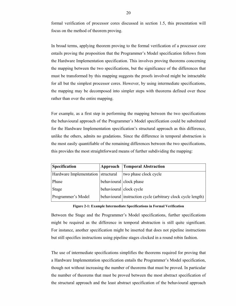
For example, as a first step in performing the mapping between the two specifications
the behavioural approach of the Programmer’s Model specification could be substituted
for the Hardware Implementation specification’s structural approach as this difference,
unlike the others, admits no gradations. Since the difference in temporal abstraction is
the most easily quantifiable of the remaining differences between the two specifications,
this provides the most straightforward means of further subdividing the mapping:
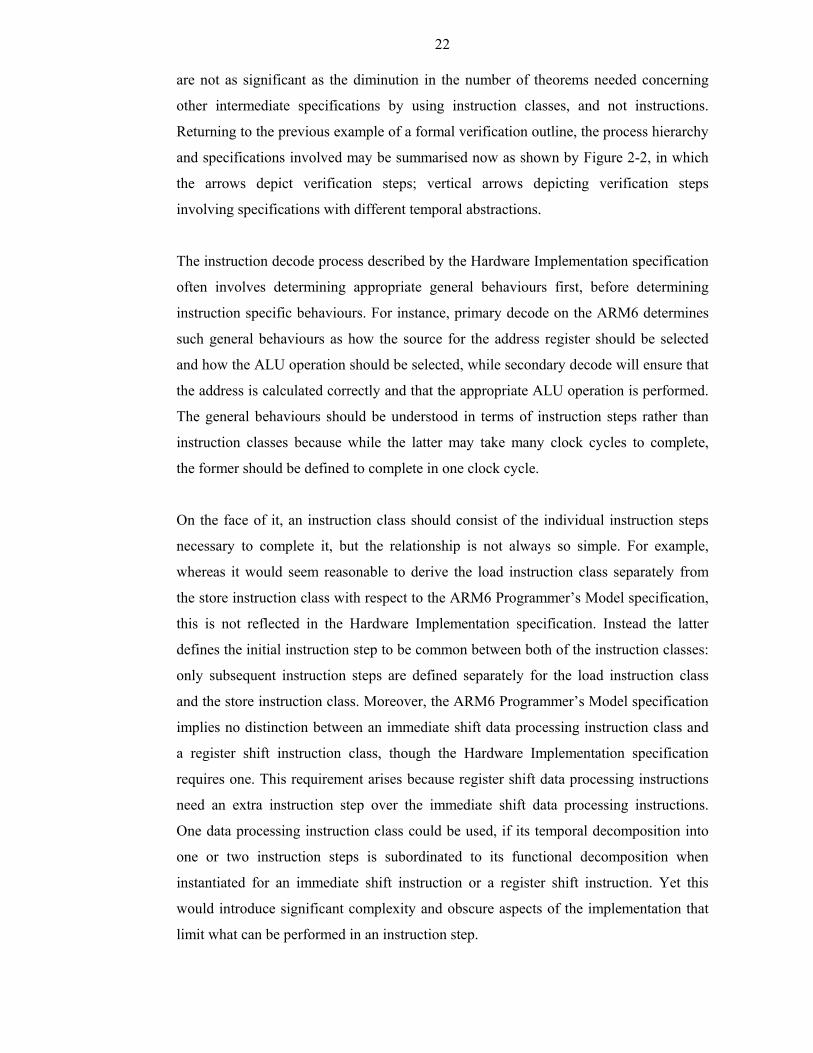
Specification Approach Temporal Abstraction
Hardware Implementation structural two phase clock cycle
Phase behavioural clock phase
Stage behavioural clock cycle
Programmer’s Model behavioural instruction cycle (arbitrary clock cycle length)
Figure 2-1: Example Intermediate Specifications in Formal Verification
Between the Stage and the Programmer’s Model specifications, further specifications
might be required as the difference in temporal abstraction is still quite significant.
For instance, another specification might be inserted that does not pipeline instructions
but still specifies instructions using pipeline stages clocked in a round robin fashion.
The use of intermediate specifications simplifies the theorems required for proving that
a Hardware Implementation specification entails the Programmer’s Model specification,
though not without increasing the number of theorems that must be proved. In particular
the number of theorems that must be proved between the most abstract specification of
the structural approach and the least abstract specification of the behavioural approach
21
are increased, which by virtue of the difference between the two specifications are likely
to be the most complex of the theorems to be proved. Continuing the previous example,
without the intermediate specifications the proof would need such theorems for each of
the instructions defined by the Programmer’s Model specification. However with
intermediate specifications the proof would need about six times as many such theorems
as each instruction would be divided into constituent pipeline stages and clock phases.
In practice, not all instruction divisions would be unique (the instruction fetch stage
would be identical for most instructions, for instance) and therefore some theorems
would be duplicated. Nevertheless, it is unlikely enough theorems would be duplicated
to radically reduce the number to be proved between the most abstract specification of
the structural approach and the least abstract specification of the behavioural approach.
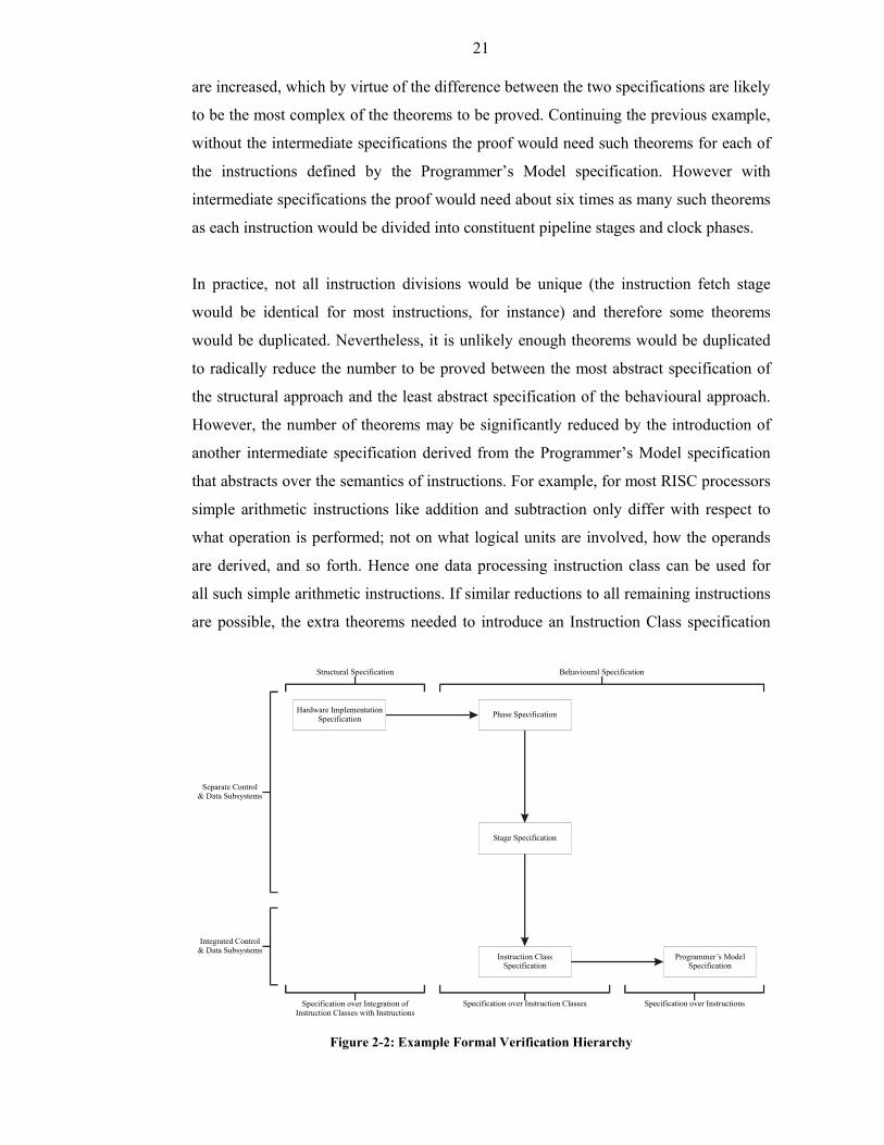
However, the number of theorems may be significantly reduced by the introduction of
another intermediate specification derived from the Programmer’s Model specification
that abstracts over the semantics of instructions. For example, for most RISC processors
simple arithmetic instructions like addition and subtraction only differ with respect to
what operation is performed; not on what logical units are involved, how the operands
are derived, and so forth. Hence one data processing instruction class can be used for
all such simple arithmetic instructions. If similar reductions to all remaining instructions
are possible, the extra theorems needed to introduce an Instruction Class specification
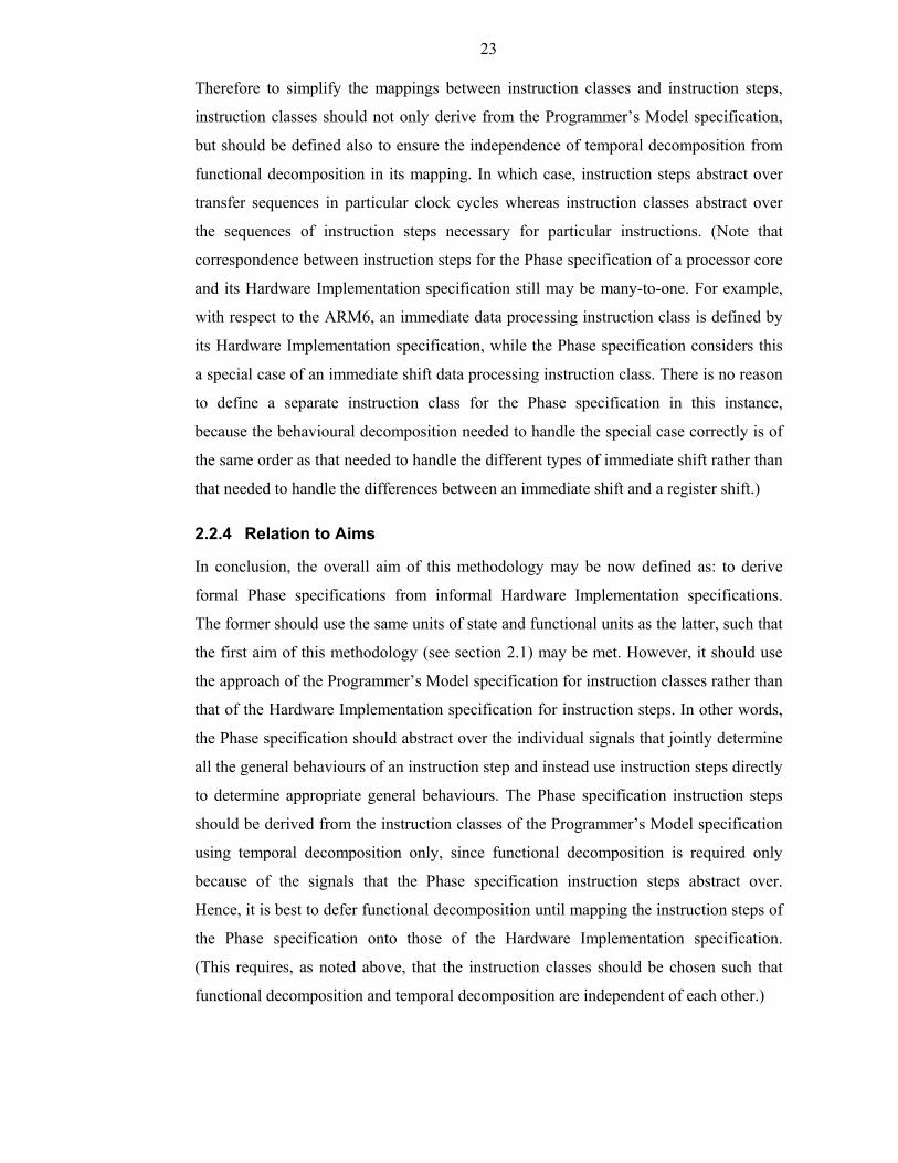
Hardware ImplementationSpecification Phase Specification
Stage Specification
Instruction ClassSpecification
Programmer’s ModelSpecification
Structural Specification Behavioural Specification
Integrated Control& Data Subsystems
Separate Control& Data Subsystems
Specification over InstructionsSpecification over Instruction ClassesSpecification over Integration ofInstruction Classes with Instructions
Figure 2-2: Example Formal Verification Hierarchy
22
are not as significant as the diminution in the number of theorems needed concerning
other intermediate specifications by using instruction classes, and not instructions.
Returning to the previous example of a formal verification outline, the process hierarchy
and specifications involved may be summarised now as shown by Figure 2-2, in which
the arrows depict verification steps; vertical arrows depicting verification steps
involving specifications with different temporal abstractions.
The instruction decode process described by the Hardware Implementation specification
often involves determining appropriate general behaviours first, before determining
instruction specific behaviours. For instance, primary decode on the ARM6 determines
such general behaviours as how the source for the address register should be selected
and how the ALU operation should be selected, while secondary decode will ensure that
the address is calculated correctly and that the appropriate ALU operation is performed.
The general behaviours should be understood in terms of instruction steps rather than
instruction classes because while the latter may take many clock cycles to complete,
the former should be defined to complete in one clock cycle.
On the face of it, an instruction class should consist of the individual instruction steps
necessary to complete it, but the relationship is not always so simple. For example,
whereas it would seem reasonable to derive the load instruction class separately from
the store instruction class with respect to the ARM6 Programmer’s Model specification,
this is not reflected in the Hardware Implementation specification. Instead the latter
defines the initial instruction step to be common between both of the instruction classes:
only subsequent instruction steps are defined separately for the load instruction class
and the store instruction class. Moreover, the ARM6 Programmer’s Model specification
implies no distinction between an immediate shift data processing instruction class and
a register shift instruction class, though the Hardware Implementation specification
requires one. This requirement arises because register shift data processing instructions
need an extra instruction step over the immediate shift data processing instructions.
One data processing instruction class could be used, if its temporal decomposition into
one or two instruction steps is subordinated to its functional decomposition when
instantiated for an immediate shift instruction or a register shift instruction. Yet this
would introduce significant complexity and obscure aspects of the implementation that
limit what can be performed in an instruction step.
23
Therefore to simplify the mappings between instruction classes and instruction steps,
instruction classes should not only derive from the Programmer’s Model specification,
but should be defined also to ensure the independence of temporal decomposition from
functional decomposition in its mapping. In which case, instruction steps abstract over
transfer sequences in particular clock cycles whereas instruction classes abstract over
the sequences of instruction steps necessary for particular instructions. (Note that
correspondence between instruction steps for the Phase specification of a processor core
and its Hardware Implementation specification still may be many-to-one. For example,
with respect to the ARM6, an immediate data processing instruction class is defined by
its Hardware Implementation specification, while the Phase specification considers this
a special case of an immediate shift data processing instruction class. There is no reason
to define a separate instruction class for the Phase specification in this instance,
because the behavioural decomposition needed to handle the special case correctly is of
the same order as that needed to handle the different types of immediate shift rather than
that needed to handle the differences between an immediate shift and a register shift.)
2.2.4 Relation to Aims
In conclusion, the overall aim of this methodology may be now defined as: to derive
formal Phase specifications from informal Hardware Implementation specifications.
The former should use the same units of state and functional units as the latter, such that
the first aim of this methodology (see section 2.1) may be met. However, it should use
the approach of the Programmer’s Model specification for instruction classes rather than
that of the Hardware Implementation specification for instruction steps. In other words,
the Phase specification should abstract over the individual signals that jointly determine
all the general behaviours of an instruction step and instead use instruction steps directly
to determine appropriate general behaviours. The Phase specification instruction steps
should be derived from the instruction classes of the Programmer’s Model specification
using temporal decomposition only, since functional decomposition is required only
because of the signals that the Phase specification instruction steps abstract over.
Hence, it is best to defer functional decomposition until mapping the instruction steps of
the Phase specification onto those of the Hardware Implementation specification.
(This requires, as noted above, that the instruction classes should be chosen such that
functional decomposition and temporal decomposition are independent of each other.)
24
Although the step from Phase specification to Hardware Implementation specification
is not trivial, it is not so radical that it would seem unreasonable to suppose an algorithm
might be developed further to this methodology to ensure the process is both verifiable
and consistent. (Of course for commercial quality processors additional optimisations
might have to be made by hand to any resulting Hardware Implementation specification,
but this would only require proving the equivalence of the affected parts of the design
at one level of abstraction.) The converse step to the Programmer’s Model specification
is more difficult and might require further intermediate specifications, as noted above,
but aided by the way in which instruction steps are derived for the Phase specification.
Therefore, the compromise between using the same units of state and functional units as
the Hardware Implementation specification and deriving all the instruction steps from
the Programmer’s Model specification helps ensure that the third aim (see section 2.1)
of this methodology may be met.
2.3 Method
It has been found useful to present the Phase specification of a processor core in one of
three ways: mathematical, engineering, and executable. Since the mathematical method
was used for the initial formulation of the Phase specification, this is discussed first and
of the three, it is the one that most easily lends itself to use in formal verification, just as
its name suggests. The engineering method involves straightforward modification of
certain aspects of the presentation of the mathematical method to make the specification
more readily understandable by those involved in processor design with no background
in formal methods. Finally the executable method builds on the engineering method and
involves presenting the specification in some programming language, and embedding
this presentation in the general simulator developed with this methodology, such that
the formal specification can be used to run programs written for the processor core
being specified. (This thesis uses the functional programming language Standard ML,
rather than an imperative language like C++, since the former provides constructs that,
if used, allow reasonably straightforward mathematical representation of any program.)
2.3.1 Mathematical
A Phase specification, like the Hardware Implementation specification it derives from,
considers a processor core in terms of two subsystems: one for data and one for control.
Following the conclusions of section 2.2.4, these two subsystems must be specified over
particular instruction classes: the behaviour of the datapath for one must be specified
25
separately to that for another and likewise for the specification of the control subsystem.
Such partitioning should pose no problem for specification of the datapath subsystem
since this involves, albeit at a lower level of abstraction, effectively the same transfers
as the Programmer’s Model specification from which the instruction classes are derived.
However not all the behaviour of the control subsystem can be specified separately for
particular instruction classes. This is because the behaviour relating to instruction flow
actually describes how the individual specifications for particular instruction classes
should be combined to indicate the total behaviour of a processor core as determined by
the contents of its pipeline at any time. Hence, any Phase specification may be divided
into three sub-specifications:
1. DATAPATH SPECIFICATION: for each instruction class describes the sequence of
transfers needed, at the Hardware Implementation specification level of abstraction,
to specify how each instruction class should change the units of state visible to
(mentioned by) the Programmer’s Model specification. Any operations used in
these transfers should be represented using uninterpreted functions.
2. DATAPATH CONTROL SPECIFICATION: for each instruction class describes the set of
interpreted functions necessary to specify the output signals of a processor core and
the interpretations of the set of functions used by the relevant datapath specification.
It also describes any sequences of transfers required by these interpreted functions
(which is not particular to any set of instructions and so cannot be specified by any
datapath specification).
3. PIPELINE CONTROL SPECIFICATION: describes the set of interpreted functions required
to specify how the entire behaviour of a processor core may be constructed from
input signals and the units of state relating to instruction flow using instruction steps.
It also describes any sequences of transfers required by these interpreted functions.
The terms listed above are used to denote the relevant fully qualified term in this thesis
for reasons of brevity. For example, ‘Datapath Control specification’ is used instead of
‘the Phase specification of the control subsystem concerning the datapath.’ Likewise for
sub-specifications that should be partitioned by instruction class, thus the partition of
the ‘Datapath Control specification for the multiplication instruction class’ is referred to
simply as the ‘Multiplication Datapath Control specification.’
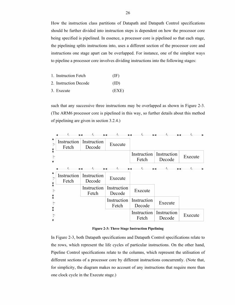
26
How the instruction class partitions of Datapath and Datapath Control specifications
should be further divided into instruction steps is dependent on how the processor core
being specified is pipelined. In essence, a processor core is pipelined so that each stage,
the pipelining splits instructions into, uses a different section of the processor core and
instructions one stage apart can be overlapped. For instance, one of the simplest ways
to pipeline a processor core involves dividing instructions into the following stages:
1. Instruction Fetch (IF)
2. Instruction Decode (ID)
3. Execute (EXE)
such that any successive three instructions may be overlapped as shown in Figure 2-3.
(The ARM6 processor core is pipelined in this way, so further details about this method
of pipelining are given in section 3.2.4.)
t1 t2 t3
i1
i2
i3
InstructionFetch
InstructionDecode Executei
1i
2i
4
t4 t5 t6
t4 t5 t6
t1 t2 t3
InstructionFetch
InstructionDecode Execute
InstructionFetch
InstructionDecode Execute
InstructionFetch
InstructionDecode Execute
InstructionFetch
InstructionDecode Execute
InstructionFetch
InstructionDecode Execute
Figure 2-3: Three Stage Instruction Pipelining
In Figure 2-3, both Datapath specifications and Datapath Control specifications relate to
the rows, which represent the life cycles of particular instructions. On the other hand,
Pipeline Control specifications relate to the columns, which represent the utilisation of
different sections of a processor core by different instructions concurrently. (Note that,
for simplicity, the diagram makes no account of any instructions that require more than
one clock cycle in the Execute stage.)
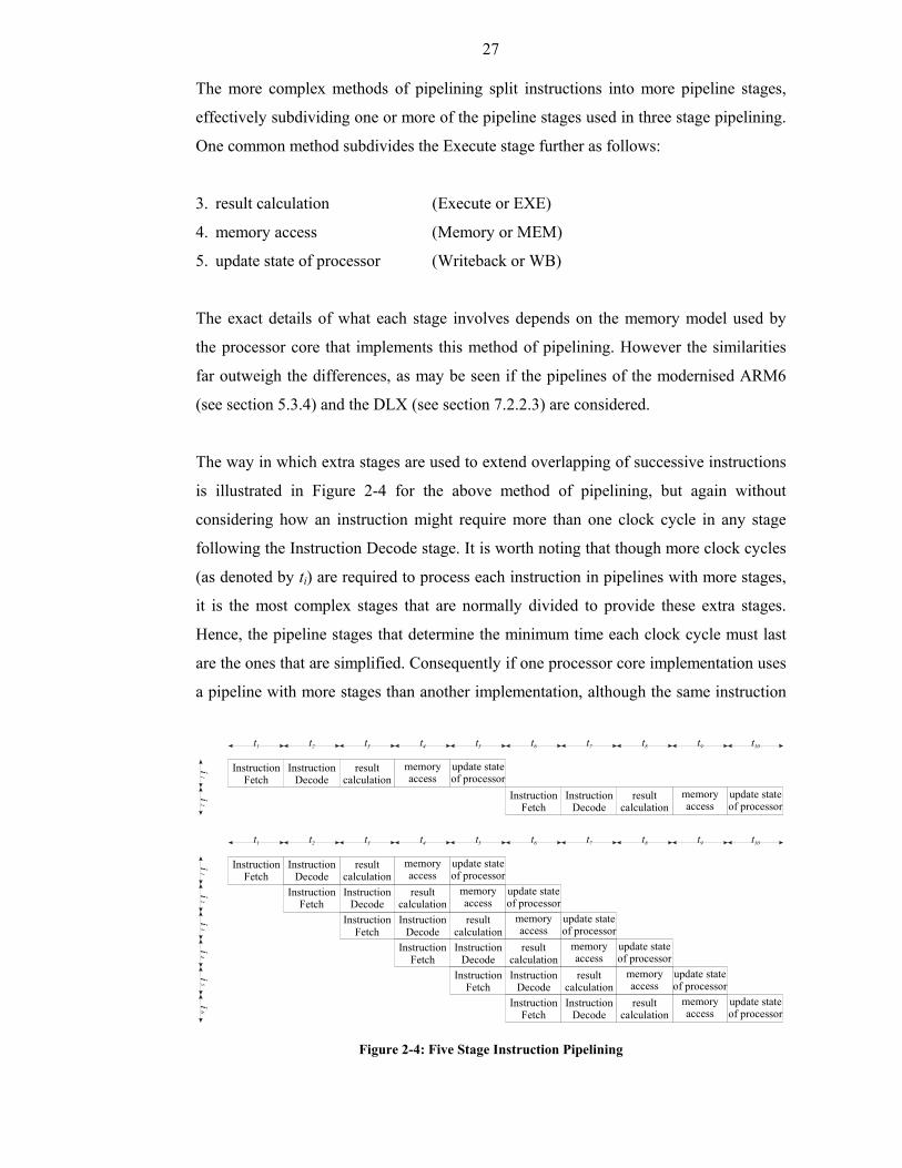
27
The more complex methods of pipelining split instructions into more pipeline stages,
effectively subdividing one or more of the pipeline stages used in three stage pipelining.
One common method subdivides the Execute stage further as follows:
3. result calculation (Execute or EXE)
4. memory access (Memory or MEM)
5. update state of processor (Writeback or WB)
The exact details of what each stage involves depends on the memory model used by
the processor core that implements this method of pipelining. However the similarities
far outweigh the differences, as may be seen if the pipelines of the modernised ARM6
(see section 5.3.4) and the DLX (see section 7.2.2.3) are considered.
The way in which extra stages are used to extend overlapping of successive instructions
is illustrated in Figure 2-4 for the above method of pipelining, but again without
considering how an instruction might require more than one clock cycle in any stage
following the Instruction Decode stage. It is worth noting that though more clock cycles
(as denoted by ti) are required to process each instruction in pipelines with more stages,
it is the most complex stages that are normally divided to provide these extra stages.
Hence, the pipeline stages that determine the minimum time each clock cycle must last
are the ones that are simplified. Consequently if one processor core implementation uses
a pipeline with more stages than another implementation, although the same instruction
resultcalculation
memoryaccess
update stateof processor
resultcalculation
memoryaccess
update stateof processor
InstructionFetch
InstructionDecode
resultcalculation
memoryaccess
update stateof processor
resultcalculation
memoryaccess
update stateof processor
resultcalculation
memoryaccess
update stateof processor
resultcalculation
memoryaccess
update stateof processor
resultcalculation
memoryaccess
update stateof processor
resultcalculation
memoryaccess
update stateof processor
t1 t2 t3 t4 t5 t6 t7 t8 t10t9
t1 t2 t3 t4 t5 t6 t7 t8 t10t9
i1
i2
i1
i2
i3
i4
i5
i6
InstructionFetch
InstructionDecode
InstructionFetch
InstructionDecode
InstructionFetch
InstructionDecode
InstructionFetch
InstructionDecode
InstructionFetch
InstructionDecode
InstructionFetch
InstructionDecode
InstructionFetch
InstructionDecode
Figure 2-4: Five Stage Instruction Pipelining
28
will need more clock cycles on the former, each clock cycle should be of less duration,
making the overall time required much less, or at worst the same.
The life cycle of an instruction on a processor core, irrespective of pipelining method,
may be described in terms of:
• PIPELINE LATCH: As an instruction completes each pipeline stage in its life cycle,
some state has to be passed on to the next stage until it completes its final stage.
Instead of considering this in terms of the individual latches used to preserve and
drive items of state for the next stage, it is useful to refer to one pipeline latch that
abstracts over all these latches.
• TIME: The ideal time in clock cycles an instruction should take to reach some stage in
its life cycle; ideal in the sense it is assumed that one clock cycle is required to fetch
the instruction and that it does not have to wait to enter the Instruction Decode stage.
(The instruction would have to wait if one of the preceding instructions required
multiple clock cycles in one of the stages following the Instruction Decode stage.)
• PIPELINE ACTIVITIES: The activities an instruction requires of a processor core in
each of the pipeline stages it enters expressed in terms of the pipelining method of
the processor core. For instance, the Instruction Fetch stage records the result of
attempting to read an instruction from memory, but the activity associated with this
will be the effect of another instruction in another pipeline stage, not of the one that
enters Instruction Fetch if the memory read succeeded.
• PRE-FETCH QUEUE: This collectively refers to the stages that an instruction enters
before it is decoded and thereby in which it cannot determine any pipeline activities.
Typically, the Instruction Fetch stage and any stages used to preserve instructions
when a preceding instruction does not complete a post Instruction Decode stage in
one clock cycle.
Hence, the life cycle of an instruction in the three stage pipeline depicted in Figure 2-3
may be described as in Table 2-1, while that of an instruction in the five stage pipeline
depicted in Figure 2-4 may be described as in Table 2-2. Note unlike either depiction,
both tables take into account what should happen if an instruction requires more than
one clock cycle in the Execute stage; m is used to denote the time when an instruction
has its last iteration in the Execute stage. (Iteration in a pipeline stage does not imply
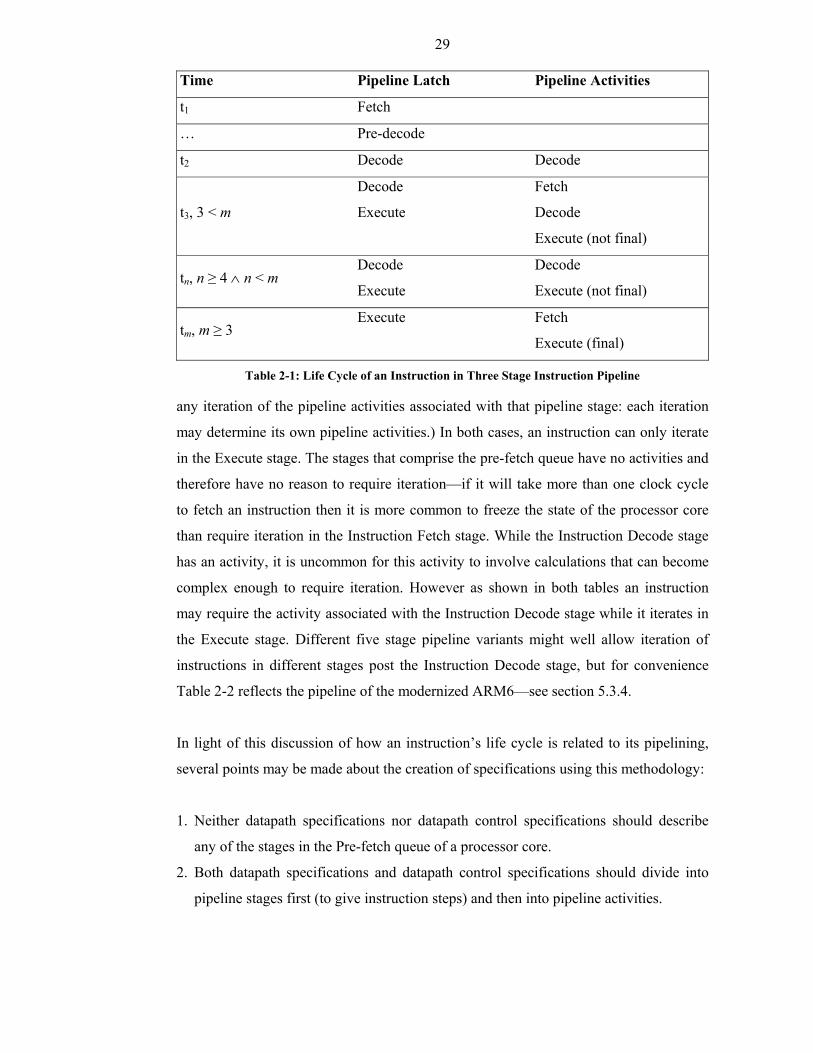
29
Time Pipeline Latch Pipeline Activities
t1 Fetch
… Pre-decode
t2 Decode Decode
t3, 3 < m
Decode
Execute
Fetch
Decode
Execute (not final)
tn, n ≥ 4 ∧ n < m Decode
Execute
Decode
Execute (not final)
tm, m ≥ 3 Execute Fetch
Execute (final)
Table 2-1: Life Cycle of an Instruction in Three Stage Instruction Pipeline
any iteration of the pipeline activities associated with that pipeline stage: each iteration
may determine its own pipeline activities.) In both cases, an instruction can only iterate
in the Execute stage. The stages that comprise the pre-fetch queue have no activities and
therefore have no reason to require iteration—if it will take more than one clock cycle
to fetch an instruction then it is more common to freeze the state of the processor core
than require iteration in the Instruction Fetch stage. While the Instruction Decode stage
has an activity, it is uncommon for this activity to involve calculations that can become
complex enough to require iteration. However as shown in both tables an instruction
may require the activity associated with the Instruction Decode stage while it iterates in
the Execute stage. Different five stage pipeline variants might well allow iteration of
instructions in different stages post the Instruction Decode stage, but for convenience
Table 2-2 reflects the pipeline of the modernized ARM6—see section 5.3.4.
In light of this discussion of how an instruction’s life cycle is related to its pipelining,
several points may be made about the creation of specifications using this methodology:
1. Neither datapath specifications nor datapath control specifications should describe
any of the stages in the Pre-fetch queue of a processor core.
2. Both datapath specifications and datapath control specifications should divide into
pipeline stages first (to give instruction steps) and then into pipeline activities.
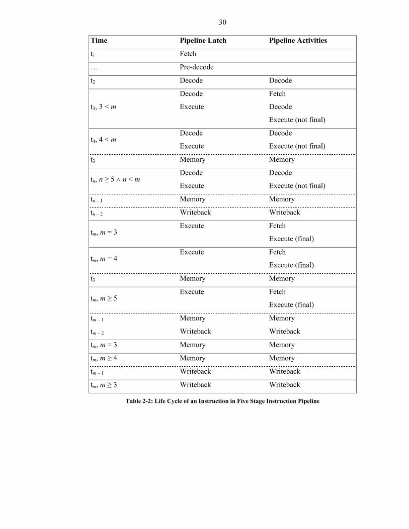
30
Time Pipeline Latch Pipeline Activities
t1 Fetch
… Pre-decode
t2 Decode Decode
t3, 3 < m
Decode
Execute
Fetch
Decode
Execute (not final)
t4, 4 < m Decode
Execute
Decode
Execute (not final)
t3 Memory Memory
tn, n ≥ 5 ∧ n < m Decode
Execute
Decode
Execute (not final)
tn – 1 Memory Memory
tn – 2 Writeback Writeback
tm, m = 3 Execute Fetch
Execute (final)
tm, m = 4 Execute Fetch
Execute (final)
t3 Memory Memory
tm, m ≥ 5 Execute Fetch
Execute (final)
tm – 1 Memory Memory
tm – 2 Writeback Writeback
tm, m = 3 Memory Memory
tm, m ≥ 4 Memory Memory
tm – 1 Writeback Writeback
tm, m ≥ 3 Writeback Writeback
Table 2-2: Life Cycle of an Instruction in Five Stage Instruction Pipeline
31
3. Pipeline control specifications should describe how the pre-fetch queue operates and
how each instruction in the pipeline, but not in the pre-fetch queue, contributes via
the activities specified by datapath specifications and datapath control specifications
to the overall behaviour of a processor core. Hence, pipeline control specifications
should define at least a NXTIC function and an IC function. The first specifies how
an instruction in the Instruction Decode stage and any other pertinent signals (such as
an indicator for data hazards—see section 5.3.4) determine the instruction class that
should govern behaviour associated with the Instruction Decode stage. The second
specifies how the latched result of NXTIC and any pertinent signals (like an indicator
whether the instruction passed its condition code) determine the instruction class that
should govern behaviour associated with the Execute stage.
a. If iterations in one or more stages are supported, pipeline control specifications
should define a NXTIS function and an IS function. These are similar in purpose
to NXTIC and IC respectively, but specify associated time, not instruction class.
Consequently the instruction step that should govern behaviour associated with
the Instruction Decode stage can be determined by combining NXTIC and NXTIS,
just as combining IC and IS provides the instruction step for the Execute stage.
(If the processor core does not support the iteration of instructions in any stage,
instruction steps and instruction classes may be conflated.)
b. Pipeline control specifications for processor cores with pipelines that have more
than three stages are unlikely to require further functions similar to NXTIC, IC,
NXTIS, or IS (unless the Instruction Decode stage is further subdivided).
Otherwise, instruction steps associated with stages following the first subdivision
of the Execute stage can be determined by just appropriately buffering IC and IS
through the relevant pipeline latches.
c. When the operations of the datapath and the control subsystem in one clock cycle
are divided into two or more phases, then IC and IS should be specified explicitly
for each clock phase. (This may just involve latching the results of IC and IS from
initial calculation in the first clock phase.) NXTIC and NXTIS, on the other hand,
only need to be specified in the clock phase instruction decode is first performed
and any subsequent clock phases.
4. Interaction between the pipeline control specification and the other specifications
should be kept simple by arranging its functions so that those which specify signals
required by the other specifications precede the NXTIC, IC, NXTIS and IS functions,
while those which require signals specified by functions in the other specifications
32
follow these functions. This is not always possible. For example, forwarding units or
hazard units (see section 5.3.4) should be specified by pipeline control specifications.
Yet, these require signals defined by functions in the datapath control specification
(such as register addressing signals) while being required by functions that specify
other signals in the datapath control specification (like write enable signals).
Therefore, to allow relatively straightforward consideration of dependencies between
the pipeline control specification and the other specifications, the functions that
specify logic such as forwarding units should be presented in separate arrangements.
Then the converse of the usual relationship may be applied: the functions defined by
the datapath control specification should be arranged so those which specify signals
required in the specification of logic such as forwarding units precede those which
use the signals produced by such logic.
Applying this to the example of a three stage pipeline in Figure 2-3: for each instant tn,
n ≥ 2 an instruction class is valid the datapath and the datapath control specifications
describe what each relevant pipeline activity entails for that particular instruction class.
The pipeline control specification requires that the instruction in the Execute latch
specifies the Fetch and the Execute activities and that Decode activities are specified by
the instruction in the Decode latch (both latches are occupied by the same instruction
when it iterates in the Execute stage). This involves the translation of the instruction in
the Decode latch into its instruction class and the association of an instruction class with
the instruction in the Execute latch. (The latter will typically just be the instruction class
derived when the instruction was in the Decode latch, but when the instruction involves
the evaluation of a condition code, for example, then the pipeline control specification
would indicate when a null instruction class must be substituted for the original one.)
Once the instruction classes have been determined, then the pertinent pipeline activities
may be determined by using both the datapath and the datapath control specifications of
these instruction classes. Finally, the pipeline control specification is responsible for
describing how the entire life cycle of an instruction is managed in terms of latches and,
when appropriate, the time the instruction has taken. (Hence, in terms introduced in
section 2.2.3, the pipeline control specification relates to the control subsystem blocks
that perform primary decode while the datapath control specification relates to those
that perform secondary decode.)
33
Having thus established the general nature of the specifications that the methodology of
this thesis can be used to develop, it is now worth considering the types of entities that
such specifications must involve:
• BUS: provides connection from one component to one or more other components
(components being either memory elements or combinatorial logic).
• COMBINATIONAL LOGIC: component used to transform its inputs in some manner and
output the result; its result at any instant reflecting the values of its inputs at that
same instant (propagation delays are assumed to be zero in this thesis).
• MEMORY ELEMENT: component used to store the value of an input for some period
and then output that stored value even if the value of its input subsequently changed.
The particular instances used depend on the Hardware Implementation specification of
the processor core being specified. However, the following list of instances defined for
the ARM6 processor core should be reasonably representative.
• COMBINATIONAL LOGIC
♦ Functional Units: combinational logic best described with respect to its function
rather than its composition in terms of logic gates. For example: barrel shifter;
arithmetic logic unit (ALU); zero-padder; sign-extender and so forth.
♦ Multiplexers: combinational logic best described with respect to how its inputs
combine to form its output, rather than its composition in terms of logic gates.
♦ Static Logic: combinational logic best described with respect to its composition
in terms of logic gates. (Unlike functional units or multiplexers, these components
are often created for particular processor cores and cannot be reused for
significantly different processor cores.)
• MEMORY ELEMENTS
♦ Latch: memory element that constantly outputs a stored value of its data input,
except when it is transparent, then the value stored changes to the value driven on
the data input and this possibly changing value is transferred to the output instead.
In general, because clock cycles on the ARM6 are subdivided into two phases,
this component is transparent in one phase whilst its output is stable in the other.
34
CONDITIONAL LATCH: latch that allows the value to be stored to be set only if
some condition is met. (The latch may also never be transparent in one phase,
just as the more general kind of latch.)
R-S LATCH: latch that allows an individual bit of the value stored to be set
without affecting any of its other bits, or all bits of the value stored to be reset
at the same time. These two actions may be requested independently such that
one of the two should be defined to have priority, if both can be requested in
the same clock phase.
The entities considered so far derive from the Hardware Implementation specification,
but certain entities are best treated in terms of the Programmer’s Model specification,
despite the differences in the level of abstraction; these entities include main memory,
register banks or caches. Although these entities may be implemented using RAM cells
or gated registers, the interaction with the other entities at the RTL level of abstraction
is in terms of some well-defined interface and not this implementation. Such interfaces
describe the signals that should be used to perform transfers between the entities and
thus it is the implementation of such interfaces, as far as it concerns the processor core,
which must be specified when the methodology of this thesis is used. In general terms,
the datapath specification describes when the interface is used to perform transfers,
whereas the datapath control specification describes the implementation of the interface
in terms of its signals. (Note this should be true even in the case of instruction fetches,
since these are performed when an instruction reaches a particular point in its life cycle.
Still the pipeline control specification may need to specify how the result is latched,
depending on how the associated block of pipeline latches is implemented.)
In order that all connections used for transfers be specified to the same level of detail,
transfers always must be specified as either proceeding from a bus or to a bus. Note that
both outputs of and inputs to the processor core are essentially the same type of entity
as buses, but are denoted boldface to make clear that these, unlike buses, are not just
internal to the processor core. Still to avoid unnecessary complexity the same name,
rather than different names for each, may be used for a latch, the bus that may be used
to drive it in one phase and the bus that it drives in another phase, because the entity
referred to can be determined from the context in most situations. (Generally, the buses
are valid in distinct phases—the first when the latch is transparent and the second when
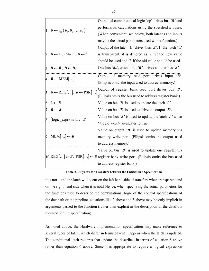
35
1 ( )op 1 2f , , , nB B B B← …
Output of combinational logic ‘op’ drives bus ‘B’ and
performs its calculations using the specified n buses.
(When convenient, see below, both latches and inputs
may be the actual parameters used with a function.)
2 LB ← , B L← , B l←
Output of the latch ‘L’ drives bus ‘B’. If the latch ‘L’
is transparent, it is denoted as ‘L’ if the new value
should be used and ‘l’ if the old value should be used.
3 B ← B , 0B B← One bus ‘B0’, or an input ‘B’, drives another bus ‘B’.
4 [ ]MEM← …B Output of memory read port drives input ‘B’.
(Ellipsis omits the input used to address memory.)
5 [ ]REGB ← … , [ ]PSRB ← …Output of register bank read port drives bus ‘B’.
(Ellipsis omits the bus used to address register bank.)
6 L B← Value on bus ‘B’ is used to update the latch ‘L’.
7 B←B Value on bus ‘B’ is used to drive the output ‘B’.
8 logic_expr L B⇒ ← Value on bus ‘B’ is used to update the latch ‘L’ when
‘<logic_expr>’ evaluates to true.
9 [ ]MEM ←… B Value on output ‘B’ is used to update memory via
memory write port. (Ellipsis omits the output used
to address memory.)
10 [ ]REG B←… , [ ]PSR B←…Value on bus ‘B’ is used to update one register via
register bank write port. (Ellipsis omits the bus used
to address register bank.)
Table 2-3: Syntax for Transfers between the Entities in a Specification
it is not—and the latch will occur on the left hand side of transfers when transparent and
on the right hand side when it is not.) Hence, when specifying the actual parameters for
the functions used to describe the combinational logic of the control specifications of
the datapath or the pipeline, equations like 2 above and 3 above may be only implicit in
arguments passed to the function (rather than explicit in the description of the dataflow
required for the specification).
As noted above, the Hardware Implementation specification may make reference to
several types of latch, which differ in terms of what happens when the latch is updated.
The conditional latch requires that updates be described in terms of equation 8 above
rather than equation 6 above. Since it is appropriate to require a logical expression
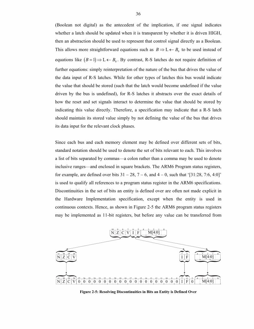
36
(Boolean not digital) as the antecedent of the implication, if one signal indicates
whether a latch should be updated when it is transparent by whether it is driven HIGH,
then an abstraction should be used to represent that control signal directly as a Boolean.
This allows more straightforward equations such as 0LB B⇒ ← to be used instead of
equations like ( ) 01 LB B= ⇒ ← . By contrast, R-S latches do not require definition of
further equations: simply reinterpretation of the nature of the bus that drives the value of
the data input of R-S latches. While for other types of latches this bus would indicate
the value that should be stored (such that the latch would become undefined if the value
driven by the bus is undefined), for R-S latches it abstracts over the exact details of
how the reset and set signals interact to determine the value that should be stored by
indicating this value directly. Therefore, a specification may indicate that a R-S latch
should maintain its stored value simply by not defining the value of the bus that drives
its data input for the relevant clock phases.
Since each bus and each memory element may be defined over different sets of bits,
standard notation should be used to denote the set of bits relevant to each. This involves
a list of bits separated by commas—a colon rather than a comma may be used to denote
inclusive ranges—and enclosed in square brackets. The ARM6 Program status registers,
for example, are defined over bits 31 – 28, 7 – 6, and 4 – 0, such that ‘[31:28, 7:6, 4:0]’
is used to qualify all references to a program status register in the ARM6 specifications.
Discontinuities in the set of bits an entity is defined over are often not made explicit in
the Hardware Implementation specification, except when the entity is used in
continuous contexts. Hence, as shown in Figure 2-5 the ARM6 program status registers
may be implemented as 11-bit registers, but before any value can be transferred from
N Z C V I F
M[4:0]
N Z C V I
0
31 30 29 28 7
5 4 3 2 1 0
M[4:0]4 3 2 1 010 9 8 7 6 5
I F7 6
M[4:0]4 3 2 1 0
F6
N Z C V31 30 29 28
08
09
010
011
012
013
014
015
016
017
018
019
020
021
022
023
024
025
026
027
Figure 2-5: Resolving Discontinuities in Bits an Entity is Defined Over
37
these registers to one of the 32-bit data registers, each bit present in the 11-bit register
must be mapped to its 32-bit location and the discontinuities filled with zeroes (or ones).
However the specifications developed by the methodology of this thesis abstract over
the actual implementation of discontinuous entities, as this relates more to efficiency
than function. Consequently, the first step of Figure 2-5 is hidden by this abstraction,
and this allows the process and its converse to be denoted as follows:
[ ] [ ] [ ] [ ][ ] [ ]
2031: 0 31: 28 0 7 : 6 0 4 : 0
31: 28,7 : 6, 4 : 0 31: 28,7 : 6,4 : 0
B A A A
A B
← ++ ++ ++ ++
←
where B[31:0] is a 32-bit register and A[31:28,7:6,4:0] a 11-bit program status register
(‘++’ denotes bit concatenation and xn denotes the replication n times of the bit x).
Although it might seem that using the same notation for the qualification of
discontinuous entities and bit selection from an entity could be confusing, this is
standard practice and in general the set of bits each entity is defined over is clear when
that entity is placed in the context of the processor core it is part of. In such contexts,
one particular set of bits is often defined as characteristic of the fundamental word of
that processor core (bits 31 – 0 for the ARM6 processor core), and again following
standard practice, qualification may be omitted for word typed entities. Entities that
refer to abstractions, such as Booleans or instruction classes, rather than digital values,
should be simply qualified with ‘[*]’ to indicate clearly these have been introduced by
the Phase specification to abstract over the Hardware Implementation specification and
may have no direct relations in the latter.
The range of transfers required in the specification of a processor core may be expressed
in terms of one syntax, as discussed above, but one syntax cannot conveniently express
the different forms of combinational logic required. Table 2-4 shows the syntaxes used
in the development of the methodology of this thesis. (Of these four, only 4 is necessary
to describe combinational logic derived from the Hardware Implementation function.
Still 2 allows one complex output expression for combinational logic like multiplexers
and PLAs—Programmable Logic Arrays—to be decomposed into several simpler ones.
3 allows further simplification of 2 under certain circumstances, while 1 is useful for
specifying combinational logic dedicated to bit concatenation clearly.)
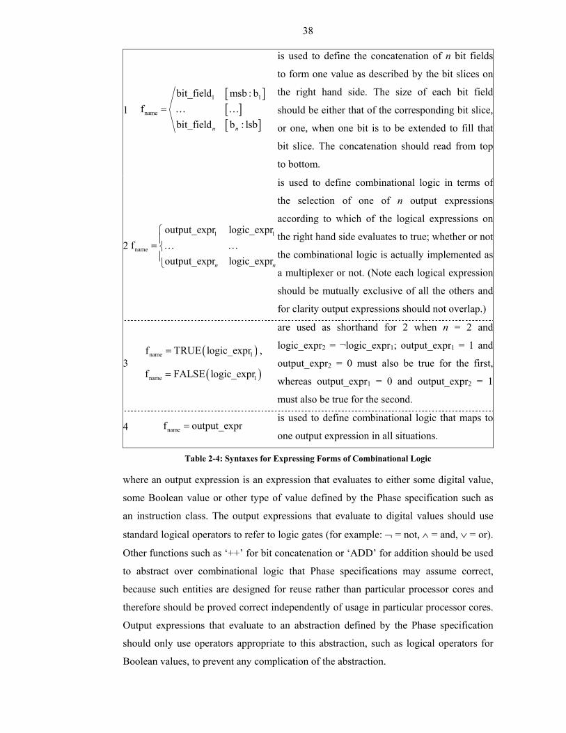
38
1 [ ][ ][ ]
1 1
name
bit_field msb : bf
bit_field b : lsbn n
= … …
is used to define the concatenation of n bit fields
to form one value as described by the bit slices on
the right hand side. The size of each bit field
should be either that of the corresponding bit slice,
or one, when one bit is to be extended to fill that
bit slice. The concatenation should read from top
to bottom.
2
1 1
name
output_expr logic_exprf
output_expr logic_exprn n
=
… …
is used to define combinational logic in terms of
the selection of one of n output expressions
according to which of the logical expressions on
the right hand side evaluates to true; whether or not
the combinational logic is actually implemented as
a multiplexer or not. (Note each logical expression
should be mutually exclusive of all the others and
for clarity output expressions should not overlap.)
3 ( )name 1f TRUE logic_expr= ,
( )name 1f FALSE logic_expr=
are used as shorthand for 2 when n = 2 and
logic_expr2 = ¬logic_expr1; output_expr1 = 1 and
output_expr2 = 0 must also be true for the first,
whereas output_expr1 = 0 and output_expr2 = 1
must also be true for the second.
4 namef output_expr= is used to define combinational logic that maps to
one output expression in all situations.
Table 2-4: Syntaxes for Expressing Forms of Combinational Logic
where an output expression is an expression that evaluates to either some digital value,
some Boolean value or other type of value defined by the Phase specification such as
an instruction class. The output expressions that evaluate to digital values should use
standard logical operators to refer to logic gates (for example: ¬ = not, ∧ = and, ∨ = or).
Other functions such as ‘++’ for bit concatenation or ‘ADD’ for addition should be used
to abstract over combinational logic that Phase specifications may assume correct,
because such entities are designed for reuse rather than particular processor cores and
therefore should be proved correct independently of usage in particular processor cores.
Output expressions that evaluate to an abstraction defined by the Phase specification
should only use operators appropriate to this abstraction, such as logical operators for
Boolean values, to prevent any complication of the abstraction.
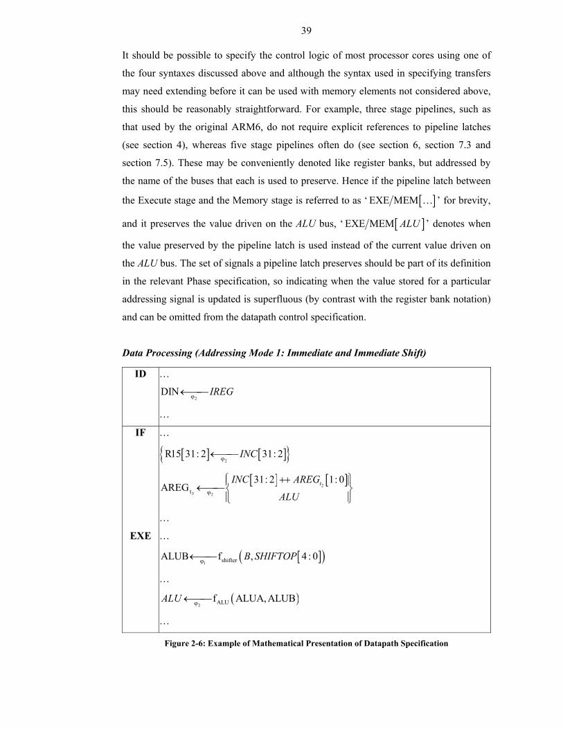
39
It should be possible to specify the control logic of most processor cores using one of
the four syntaxes discussed above and although the syntax used in specifying transfers
may need extending before it can be used with memory elements not considered above,
this should be reasonably straightforward. For example, three stage pipelines, such as
that used by the original ARM6, do not require explicit references to pipeline latches
(see section 4), whereas five stage pipelines often do (see section 6, section 7.3 and
section 7.5). These may be conveniently denoted like register banks, but addressed by
the name of the buses that each is used to preserve. Hence if the pipeline latch between
the Execute stage and the Memory stage is referred to as ‘ [ ]EXE MEM … ’ for brevity,
and it preserves the value driven on the ALU bus, ‘ [ ]EXE MEM ALU ’ denotes when
the value preserved by the pipeline latch is used instead of the current value driven on
the ALU bus. The set of signals a pipeline latch preserves should be part of its definition
in the relevant Phase specification, so indicating when the value stored for a particular
addressing signal is updated is superfluous (by contrast with the register bank notation)
and can be omitted from the datapath control specification.
Data Processing (Addressing Mode 1: Immediate and Immediate Shift)
ID …
2DIN IREGϕ←
…
IF …
[ ] [ ]{ }2
R15 31: 2 31: 2INCϕ←
[ ] [ ]2
3 2t
31: 2 1: 0AREG tINC AREG
ALUϕ
++ ←
…
EXE …
[ ]( )1 shifterALUB f , 4 : 0B SHIFTOPϕ←
…
( )2 ALUf ALUA, ALUBALU ϕ←
…
Figure 2-6: Example of Mathematical Presentation of Datapath Specification
40
From the preceding discussions of the syntax of transfers between entities (in relation to
Table 2-3) and the notation for indicating the juncture in the lifecycle of an instruction
(in relation to Table 2-1 and Table 2-2), the method for mathematical presentation of
datapath specifications illustrated in Figure 2-6 may be derived. Each row in the table
specifies one pipeline activity and the pipeline activities are grouped by pipeline stage
(indicated by the presence or absence of a border between rows). The left-hand column
is used to label the pipeline activity the row specifies and groups of rows are arranged
according to the order in which the pipeline stage associated with each is entered;
hence explicit labelling of pipeline stages is unnecessary.
The example derives from the three stage ARM6 specification, so Instruction Decode is
the first pipeline stage shown at time t2 because the only preceding pipeline stage
(Instruction Fetch at time t1) has no pipeline activities associated with it to be specified.
Each pipeline stage takes one clock cycle, but this is subdivided further into two phases
on the ARM6; hence the arrow that shows the direction of each transfer is labelled with
φ1 if the transfer occurs in phase one and φ2 if the transfer occurs in phase two.
Moreover, transfers are ordered so those that occur in phase one are specified before
those that occur in phase two. After being grouped by clock phase, data dependency and
probable timing are used to arrange further the transfers within these groups.
In general if a bus or latch is only referred to in the specification of one pipeline stage of
an instruction class, no qualification is required with respect to when, in the lifecycle of
the instruction class, the bus or latch is driven or sampled. If the pipeline stage iterates,
qualification may still be omitted provided that the pipeline activities associated with
the pipeline stage are also iterated. However when a bus or latch needs qualification,
denoting the time in unstalled cycles relative to the Instruction Fetch stage is sufficient;
letters may be used to indicate a variable number of cycles over which a pipeline stage
and associated pipeline activities may iterate. Hence the complete annotation scheme
developed for the three stage ARM6 is as summarised in Table 2-5.
To handle every form of iteration in the Execute stage that may be required by any of
the instruction classes supported by the three stage ARM6, three kinds of annotation
must be defined for the Execute stage. The first kind shown in Table 2-5 is for
instruction classes that require no iteration, such as the data processing instruction class,
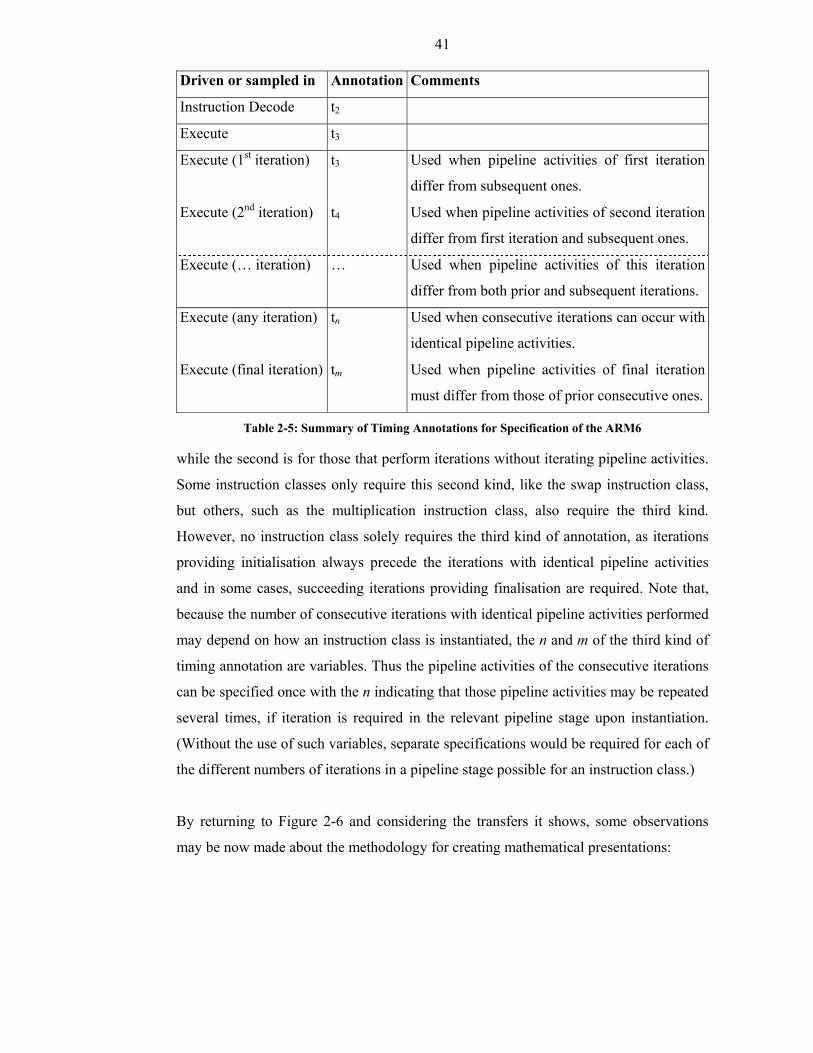
41
Driven or sampled in Annotation Comments
Instruction Decode t2
Execute t3
Execute (1st iteration) t3 Used when pipeline activities of first iteration
differ from subsequent ones.
Execute (2nd iteration) t4 Used when pipeline activities of second iteration
differ from first iteration and subsequent ones.
Execute (… iteration) … Used when pipeline activities of this iteration
differ from both prior and subsequent iterations.
Execute (any iteration) tn Used when consecutive iterations can occur with
identical pipeline activities.
Execute (final iteration) tm Used when pipeline activities of final iteration
must differ from those of prior consecutive ones.
Table 2-5: Summary of Timing Annotations for Specification of the ARM6
while the second is for those that perform iterations without iterating pipeline activities.
Some instruction classes only require this second kind, like the swap instruction class,
but others, such as the multiplication instruction class, also require the third kind.
However, no instruction class solely requires the third kind of annotation, as iterations
providing initialisation always precede the iterations with identical pipeline activities
and in some cases, succeeding iterations providing finalisation are required. Note that,
because the number of consecutive iterations with identical pipeline activities performed
may depend on how an instruction class is instantiated, the n and m of the third kind of
timing annotation are variables. Thus the pipeline activities of the consecutive iterations
can be specified once with the n indicating that those pipeline activities may be repeated
several times, if iteration is required in the relevant pipeline stage upon instantiation.
(Without the use of such variables, separate specifications would be required for each of
the different numbers of iterations in a pipeline stage possible for an instruction class.)
By returning to Figure 2-6 and considering the transfers it shows, some observations
may be now made about the methodology for creating mathematical presentations:
42
1. As already discussed, timing annotation is only used when it is necessary to avoid
confusion about when a bus or a latch is being sampled or driven; thereby preventing
superfluous detail from obscuring the presentation of the specification.
2. When a transfer needs the value of a signal from a preceding clock cycle, rather than
its value in the current clock cycle, the appropriate timing annotation should be used
to qualify direct references to this signal in the datapath specification. For instance,
the second transfer depicted for the Instruction Fetch activity requires the value of
the bottom two bits of the AREG bus from the clock cycle that immediately precedes
the activity, thus it refers to [ ]2t
1: 0AREG . This has the advantage of clarifying
which signals are buffered and which are original, as well as indicating the extent of
any buffering. However the datapath control specification should note the method
used to buffer the value of a signal, so the completeness of the overall specification
is not affected.
3. Timing annotation should not be used with functions in the datapath specification,
since functions should be used to describe combinational logic only (that is logic
which does not involve any memory elements). Sequential logic should be described
by transfers specified as part of the datapath specification or part of the dataflow
associated with the datapath control specification (and may require timing annotation
because it does involve memory elements).
4. Complete definition of operations such as fALU (…) and fshifter(…) is shared between
the datapath specification and the datapath control specification, with the latter
supplying the interpretations of the operations that the former leaves uninterpreted.
Therefore the name used for the operation in both specifications should be identical,
and unique, so that an operation in the datapath specification and its interpretation in
the datapath control specification may be readily associated. However, the nature of
the parameter list given for an operation may differ between the two specifications.
Whereas in the parameter list of an operation, the second specification should refer to
every signal used by the interpretation of the operation, the first specification should
refer to the subset of these signals associated with dataflow only and not control.
(Although the parameter list shown for the fshifter operation may appear to contravene
this requirement, in general shift operations are often expressed with two parameters:
the value to shift—in this case, that on the B bus—and the amount of shift to apply—
in this example, that on the SHIFTOP[4:0] bus. Hence to refer to the B bus only in
the parameter list might be misunderstood as indicating that the amount of shift that
can be applied is fixed.)
43
5. A datapath specification of an instruction class should be general enough to include
minor variations, and hence avoid unwarranted proliferation of instruction classes.
However, it should not be so general that, even when considered in conjunction with
all other contributors to an overall specification of a processor core, the completeness
of that overall specification is compromised. For instance, the transfer that specifies
the output of the shifter combinational logic (fshifter) drives the ALUB latch, refers to
the B bus rather than either of the two buses that may drive the value of the B bus.
It is the datapath control specification of this instruction class which specifies when
the B bus takes the value of the RB bus and when it takes the value of the IMM bus,
according to which variants of the data processing instruction class use an immediate
and which a third register value. Doing this for every transfer that involves a bus
driven by a multiplexer, may make datapath specifications hard to understand due to
the increased number of indirect references using datapath control specifications.
Hence, for convenience, when one bus will be always selected to drive another bus
(or latch), irrespective of how an instruction class may be instantiated, then that bus
may be referred to directly by that instruction class. For example, 1
ALUA RAϕ←
could be used for the data processing instruction class instead of 1
ALUA Aϕ← ,
because the RA bus will be selected always to drive the A bus.
6. Though, as noted in 5 above, the number of instruction classes may be minimised by
the appropriate use of references in the datapath specification, when this is applied to
complex processor cores the readability of the datapath specification may suffer.
Therefore whenever the function definition itself in the datapath control specification
appears simpler than the process of referencing it with an uninterpreted function in
the datapath specification, the imprecision inherent in substituting the definition for
the reference is outweighed by increased readability. In general, most, if not all,
references to multiplexers may be replaced by a vector listing each of the values that
it may select for its result. (To avoid confusion the vector should be enclosed with
curly braces as shown in the second transfer listed for the Instruction Fetch activity.)
Most other instances of combinational logic are more varied in how a result is driven,
and thus it is not appropriate to substitute associated definitions for the references in
the datapath specification. (An exception may be made when the instruction class
reduces the definition of the combinational logic for this instruction class to driving
one of its inputs as its output; so when appropriate ( )2 ALUf ALUA, ALUBALU ϕ←
might be replaced with 2
ALUBALU ϕ← .)
44
7. When curly braces enclose an entire transfer, such as with the first transfer shown for
the Instruction Fetch activity, this indicates that the transfer may or may not occur
depending on the value of the write enable signal the datapath control specification
associates with the latch. Consequently, just as when curly braces are used to enclose
the range of options a multiplexer may select from, curly braces around a transfer
indicate that the datapath specification does not completely describe the transfer and
the datapath control specification should be consulted. The 0LB B⇒ ← form of
specifying transfers could be used to make the role of the write enable signal explicit,
but this would introduce terms from the datapath control specification unnecessarily.
While the reference should be clearly noted, in most cases it should be inferable from
the name used for the latch (or register) in the datapath specification and the name
used for the write enable signal in the datapath control specification. (For example,
the R15 of the first transfer depicted for the Instruction Fetch activity is paired with
the PCWEN[0] write enable signal in the relevant datapath control specification.)
Note that curly braces are not used thus when the datapath control specification of
an instruction class ties a write enable signal to one value, such that depending on
this value the associated transfer always occurs or never occurs. If it always occurs,
the relevant datapath specification should describe the transfer with no enclosing
curly braces, and if it never occurs, the transfer should be omitted altogether.
8. The use of curly braces to indicate that dataflow depends on how an instruction class
is instantiated may be used to indicate when pipeline activities may or may not occur,
just by enclosing the labels associated with those pipeline activities in curly braces.
a. This use of curly braces may be needed in the specification of processor cores that
allow one or more pipeline stages preceding the final pipeline stage to iterate with
identical pipeline activities. For instance, the modernised ARM6 may iterate in
the Execute stage (which is the third of five) and it supports instruction classes
implemented by iteration in the Execute stage with identical pipeline activities.
However, as Table 2-2 shows, the set of pipeline activities an instruction class
determines in the Execute stage differs at time t5 and later in its life cycle from
time t3 or time t4. Consequently the timing annotation tn cannot be used in the way
outlined above until time t5, unless it is possible to indicate that pipeline activities
(such as the Writeback pipeline activity at time t4) do not apply in every case.
Although the pipeline control specification indicates which pipeline activities
apply when, and therefore indirectly what curly braces used in this way refer to,
the purpose should be noted directly in the datapath specification as well.
45
b. Processor cores may have structural hazards that prevent an instruction class
progressing from one pipeline stage to the next, even when all the results from
that stage are ready. For example, as noted in Table 5-4, the modernised ARM6
requires any instruction class that alters the operating mode of the processor core
to do so after at least one iteration in the Execute stage. However, an instance of
the data processing instruction class only needs one iteration in the Execute stage
to write the CPSR (see section 3.1.3) and calculate the result that should be stored
in the destination register during the Writeback stage. This is so even if the write
to the CPSR involves restoring the SPSR rather than just updating the status flags
and the destination register is the program counter such that the register update
occurs in the Execute stage to optimise pipeline flushing. The required delaying of
writing the CPSR to the second iteration in the Execute stage could be handled by
defining two separate data processing instruction classes, but this would involve
unnecessary duplication in respect of the pipeline activities of the first iteration in
the Execute stage. Hence, the most elegant solution is to have only one definition,
but with the labels of the pipeline activities of the second iteration enclosed in
curly braces and the circumstances under which these pipeline activities apply
clearly noted.
9. If explicit references to pipeline latches are used, then any buffering required before
the value of a bus could be preserved by a pipeline latch may be left implicit for
simplicity of presentation. For example, the modernised ARM6 requires the value
driven on the ALU bus in the Execute stage to be preserved until the Writeback stage,
utilising the [ ]EXE MEM … pipeline latch and the [ ]MEM WB … pipeline latch.
However, while the ALU bus is driven in φ2 of the Execute stage, and so no buffering
is required before its value may be preserved by the [ ]EXE MEM … pipeline latch,
the value preserved by this pipeline latch will be driven in φ1 of the Memory stage.
Hence, this value would need to be buffered to preserve it to φ2 of the Memory stage,
before it could be preserved by the [ ]MEM WB … pipeline latch. If made explicit,
however, this would obscure the direct relationship between the original value driven
in φ2 of the Execute stage and the value used in φ1 of the Writeback stage.
Most of these points, apart from 3 and 4, are not fundamental to the methodology for
creating a mathematical presentation of the Phase specification of a processor core.
However, such points are still important because one of the aims for this methodology
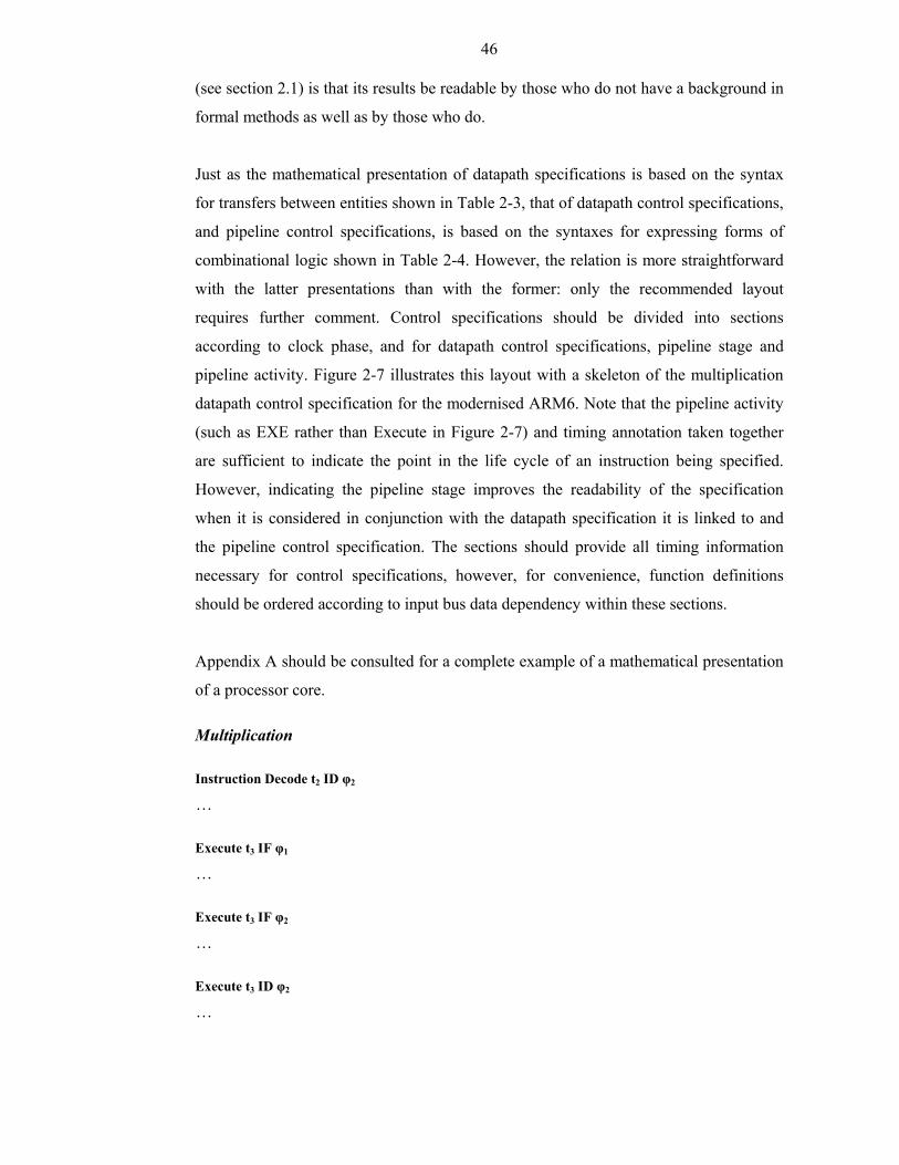
46
(see section 2.1) is that its results be readable by those who do not have a background in
formal methods as well as by those who do.
Just as the mathematical presentation of datapath specifications is based on the syntax
for transfers between entities shown in Table 2-3, that of datapath control specifications,
and pipeline control specifications, is based on the syntaxes for expressing forms of
combinational logic shown in Table 2-4. However, the relation is more straightforward
with the latter presentations than with the former: only the recommended layout
requires further comment. Control specifications should be divided into sections
according to clock phase, and for datapath control specifications, pipeline stage and
pipeline activity. Figure 2-7 illustrates this layout with a skeleton of the multiplication
datapath control specification for the modernised ARM6. Note that the pipeline activity
(such as EXE rather than Execute in Figure 2-7) and timing annotation taken together
are sufficient to indicate the point in the life cycle of an instruction being specified.
However, indicating the pipeline stage improves the readability of the specification
when it is considered in conjunction with the datapath specification it is linked to and
the pipeline control specification. The sections should provide all timing information
necessary for control specifications, however, for convenience, function definitions
should be ordered according to input bus data dependency within these sections.
Appendix A should be consulted for a complete example of a mathematical presentation
of a processor core.
Multiplication
Instruction Decode t2 ID φ2
…
Execute t3 IF φ1
…
Execute t3 IF φ2
…
Execute t3 ID φ2
…
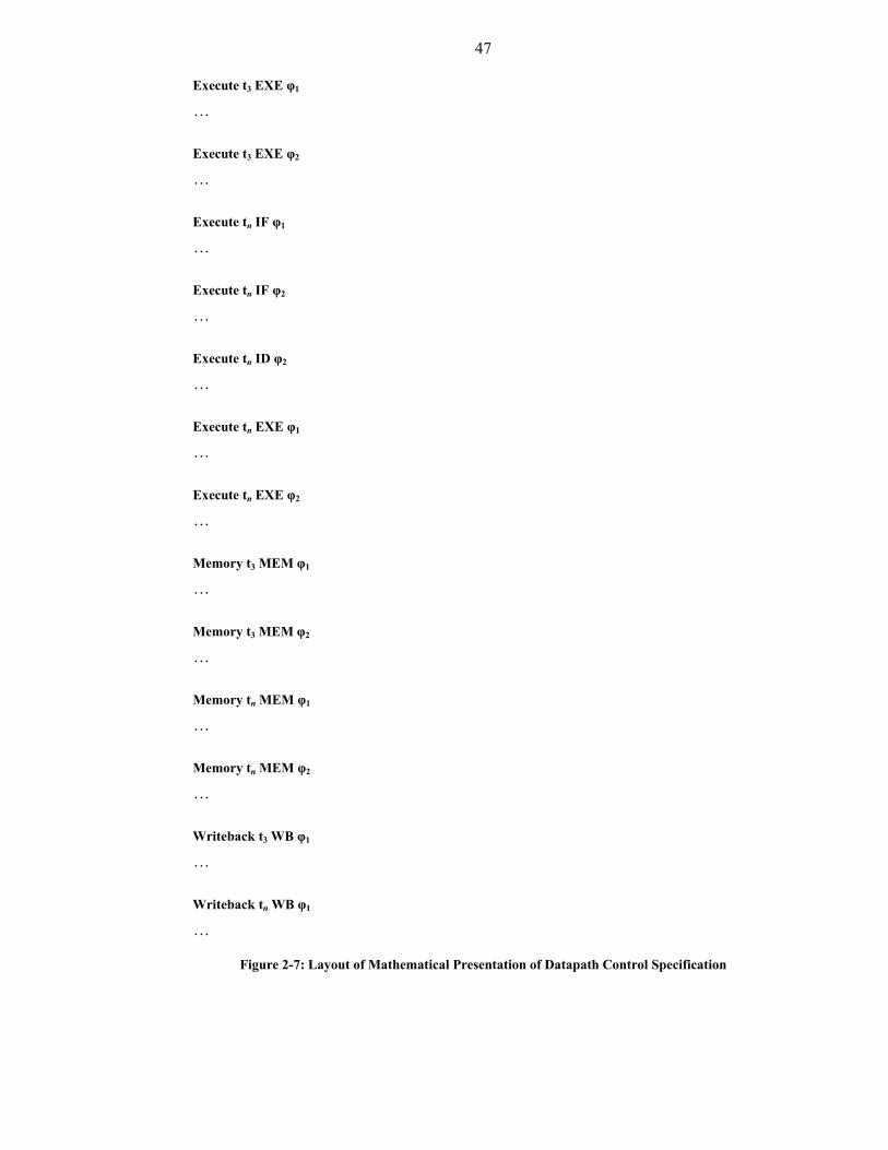
47
Execute t3 EXE φ1
…
Execute t3 EXE φ2
…
Execute tn IF φ1
…
Execute tn IF φ2
…
Execute tn ID φ2
…
Execute tn EXE φ1
…
Execute tn EXE φ2
…
Memory t3 MEM φ1
…
Memory t3 MEM φ2
…
Memory tn MEM φ1
…
Memory tn MEM φ2
…
Writeback t3 WB φ1
…
Writeback tn WB φ1
…
Figure 2-7: Layout of Mathematical Presentation of Datapath Control Specification
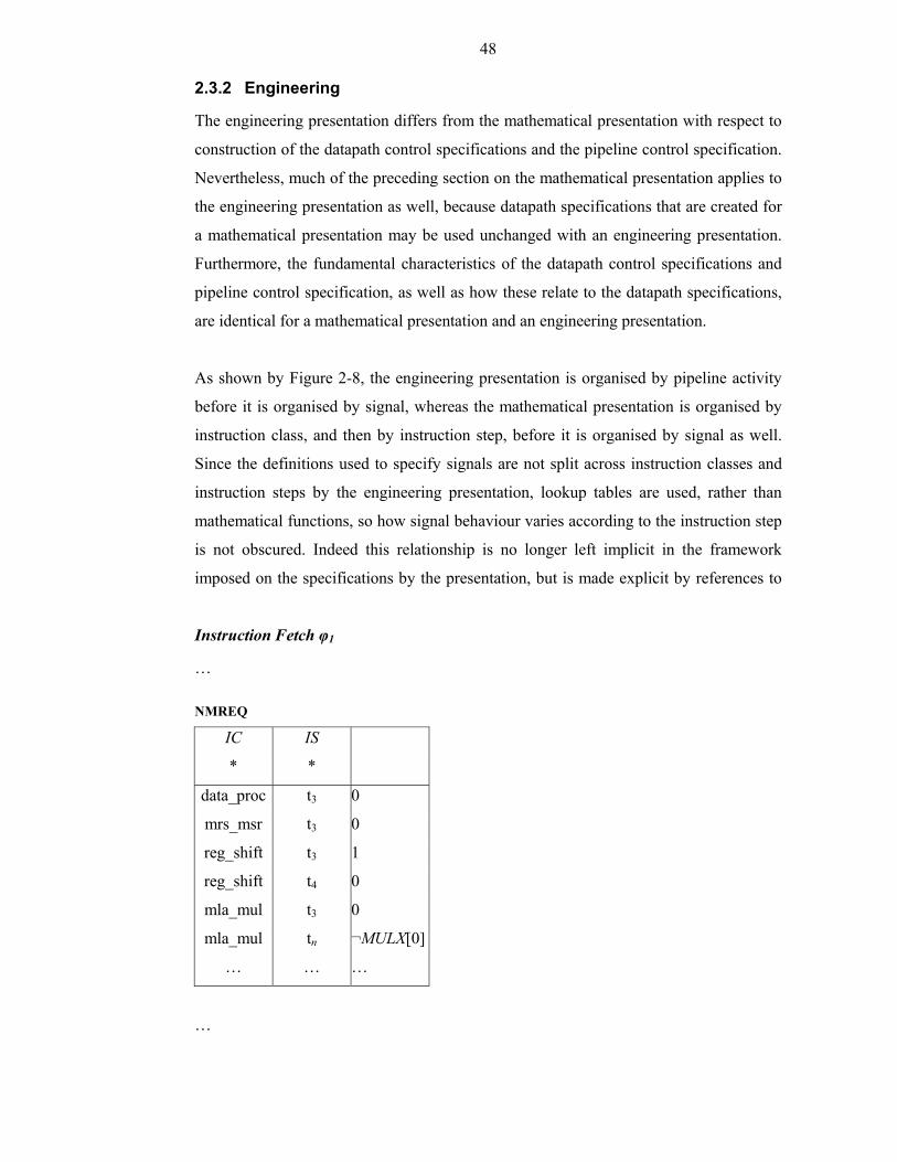
48
2.3.2 Engineering
The engineering presentation differs from the mathematical presentation with respect to
construction of the datapath control specifications and the pipeline control specification.
Nevertheless, much of the preceding section on the mathematical presentation applies to
the engineering presentation as well, because datapath specifications that are created for
a mathematical presentation may be used unchanged with an engineering presentation.
Furthermore, the fundamental characteristics of the datapath control specifications and
pipeline control specification, as well as how these relate to the datapath specifications,
are identical for a mathematical presentation and an engineering presentation.
As shown by Figure 2-8, the engineering presentation is organised by pipeline activity
before it is organised by signal, whereas the mathematical presentation is organised by
instruction class, and then by instruction step, before it is organised by signal as well.
Since the definitions used to specify signals are not split across instruction classes and
instruction steps by the engineering presentation, lookup tables are used, rather than
mathematical functions, so how signal behaviour varies according to the instruction step
is not obscured. Indeed this relationship is no longer left implicit in the framework
imposed on the specifications by the presentation, but is made explicit by references to
Instruction Fetch φ1
…
NMREQ
IC IS
* *
data_proc t3 0
mrs_msr t3 0
reg_shift t3 1
reg_shift t4 0
mla_mul t3 0
mla_mul tn ¬MULX[0]
… … …
…
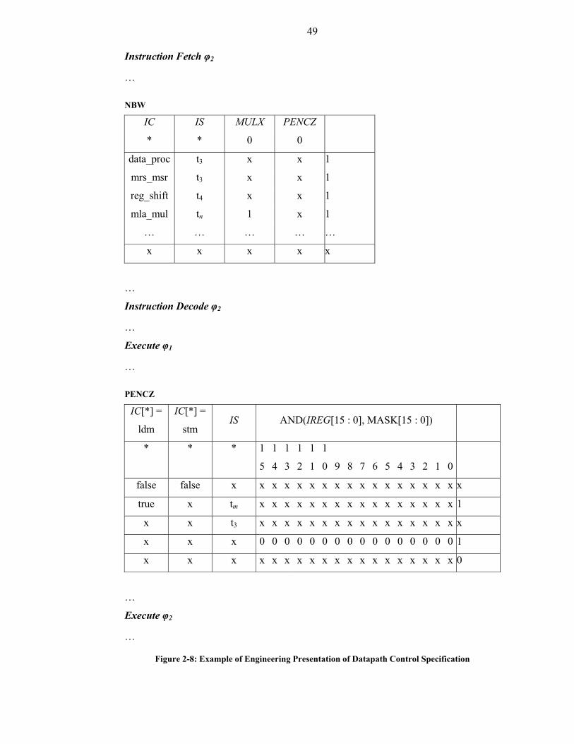
49
Instruction Fetch φ2
…
NBW
IC IS MULX PENCZ
* * 0 0
data_proc t3 x x 1
mrs_msr t3 x x 1
reg_shift t4 x x 1
mla_mul tn 1 x 1
… … … … …
x x x x x
…
Instruction Decode φ2
…
Execute φ1
…
PENCZ
IC[*] =
ldm
IC[*] =
stm IS AND(IREG[15 : 0], MASK[15 : 0])
* * * 1
5
1
4
1
3
1
2
1
1
1
0 9 8 7 6 5 4
3
2
1
0
false false x x x x x x x x x x x x x x x x x x
true x tm x x x x x x x x x x x x x x x x 1
x x t3 x x x x x x x x x x x x x x x x x
x x x 0 0 0 0 0 0 0 0 0 0 0 0 0 0 0 0 1
x x x x x x x x x x x x x x x x x x x 0
…
Execute φ2
…
Figure 2-8: Example of Engineering Presentation of Datapath Control Specification
50
IC[*] and IS[*] as required. Consequently, while the mathematical presentation of
datapath control specifications is more useful in ascertaining the signal behaviours that
an instruction class is comprised of, the engineering presentation is more useful in
determining how the behaviour of one signal should differ according to instruction class
(and instruction step).
Note, if the processor core being specified divides its clock cycle into several phases,
the pipeline activities used to organise the engineering presentation also must be divided
as shown by Figure 2-8 (the ARM6 processor core uses a clock cycle of two phases.)
Often processor cores that use multiple clock phases are designed so that the validity of
the value driven by combinational logic does not need to be assured in the clock phases
that the values of the inputs to the combinational logic are changing. The lookup table
specifying the combinational logic should only be included when the value driven by
combinational logic does need to be assured. Thus, in most cases, each lookup table
should be defined in only one of the clock phase divisions of the pipeline activity
associated with the combinational logic specified by the lookup table.
To make engineering presentations more accessible to those with no background in
formal methods, the lookup tables that form the basis of the engineering presentations
should be similar to the truth tables that are part of any background in processor design.
However, some minor differences should be observed to facilitate the creation of
concise specifications using the engineering presentation. For example, lookup tables,
like the mathematical functions of mathematical presentations, should be specified with
actual parameters rather than the formal parameters normally used with truth tables.
This clarifies which signals determine the arguments a function abstraction is applied to,
and thus which signals are used by the combinational logic (that the function represents)
to determine the signal it drives, without requiring analysis of pertinent function calls in
relevant datapath specifications. Furthermore, it removes any requirement to define
explicit signals for any simple expressions used to derive arguments only infrequently
or that result from some abstraction over the Hardware Implementation specification
(see the definition of fPENCZ in Figure 2-8). Likewise, simple expressions may be used in
the results column of the lookup table, as well as explicit values, unlike truth tables
(illustrated by the definition of fNMREQ in Figure 2-8).
51
Lookup tables should not have more than one results column and this results column
should not be labelled, since the name of the signal driven by the combinational logic
represented by the function is supplied by the heading that introduces the lookup table.
While truth tables may have multiple results columns, and thus each must be labelled,
using this approach for the lookup tables of the engineering presentation would lessen
the correspondence with the mathematical functions of the mathematical presentation.
Therefore, to represent combinational logic that drives several signals at the same time,
n-tuples should be used to label the signals—FWDAEN and FWDA in f(FWDAEN, FWDA)—
and the results—for example, (1’b0, 32’hxxxx_xxxx)—since these can be used with
both mathematical functions and lookup tables.
Whereas the use of ‘x’ in the argument columns of lookup tables to indicate matching
any of the values that may be supplied for the relevant arguments is also standard for
truth tables, the use of non-mutually exclusive matches in the same definition is not.
Nevertheless, as exemplified by the definition of fPENCZ in Figure 2-8, fewer matches
need to be defined when non-mutually exclusive matches are used in conjunction with
the rule that the first match encountered in scanning the lookup table from top to bottom
is the one that applies. (This rule has precedent in the semantics of case statements in
both the Verilog hardware description language and the ML programming language,
for instance, so it should not be counterintuitive to the users of this methodology.)
Though the mathematical presentation splits the definition of the mathematical function
specifying a signal’s behaviour across all relevant instruction steps, each sub-definition
should be mathematically complete since it is referred to IC[*] and IS[*] by its placing
(in the layout of the specification) and not as one of the actual parameters used with it.
Nonetheless, considering the sum of the sub-definitions associated with the definition of
a mathematical function is not enough to guarantee the completeness of this definition,
unless some mapping is assumed for instruction steps with no associated sub-definition.
In these cases, the result of the function should be “don’t care” in the strongest sense,
implying that, regardless of the actual value the signal corresponding to the function
may take when the implementation is synthesised, the correctness of instruction steps
with no associated sub-definitions is still guaranteed. Since the engineering presentation
does not split the definition of lookup tables across instruction steps, it is convenient for
these cases to be made explicit using ‘x’ in the results column—just as discussed above
in respect of the arguments columns—not omitted as per the mathematical presentation.
52
(As noted above, specifying processor cores with clock cycles divided into phases
requires the definition of lookup tables to be split across pipeline activities divided by
clock phase. In such cases, the same considerations for splitting the definition of
mathematical functions across instruction steps apply in ensuring the completeness of
each lookup table definition.)
When an instruction class iterates in a pipeline stage and all the iterations involve
identical pipeline activities, the last iteration may not involve all the pipeline activities
involved in the preceding iterations. For example, referring to the instruction life cycle
shown in Table 2-2, it is clear that (as is the case for the multiplication instruction class
on the modernised ARM6) the last iteration in the Execute stage may be identical to
the preceding iterations but can not involve the Decode pipeline activity. In such cases,
the pipeline control specification should indicate that the responsibility for determining
the behaviour of the omitted pipeline activity belongs to some pipeline stage other than
the one in which the iteration occurred. Thus, whereas lookup tables may be defined for
the pipeline activity that will be omitted, in the specification of an instruction class that
iterates with identical pipeline activities, these will not be referred to in the last iteration.
Hence, contention between these lookup tables and those for the specification that
determines the behaviour of the omitted pipeline activity is not possible (but, if it were,
this would indicate a structural hazard in the pipelining of the relevant processor core).
To make this clear in lookup tables, the standard notation ‘z’ for high impedance values
(normally used with tristate buses) may be used to indicate matches that never should be
referred to. The same approach may be used also with the mathematical functions of
mathematical presentations.
Appendix B should be consulted for a complete example of an engineering presentation
of a processor core.
2.3.3 Executable
Both the mathematical presentation and the engineering presentation are executable
insofar as the behaviour of a processor core specified by either, given an initial state,
should be fully determinable from the specification alone. The executable presentation,
on the other hand, represents a specification using a high-level programming language,
within the framework of a general simulator, such that the work necessary to simulate
the behaviour of the processor core specified might be automated using a computer.
53
Therefore, the strategy for the creation of the executable presentation is best discussed
with reference to the framework provided by the general simulator.
The programming language chosen for the development of the general simulator
discussed in this thesis, and thus for the executable specifications created for this thesis
as well, was Standard ML. Although this thesis only discusses executable presentations
with reference to Standard ML for this reason, the essence of this discussion applies
regardless of the programming language used to create an executable presentation—
particularly if care is taken to preserve as much of the interface of the general simulator
as is possible when implementing it in the relevant programming language.
The reusable modules of the general simulator are summarised in Table 2-6. Note that
the *_ prefix indicates that different versions of the same abstract type should be
defined for use with each different instance of an entity required by the processor core
being specified. In particular, different versions of the *_bank, the *_writeport_signals
and the *_readport_signals abstract types should be defined for each distinct bank of
physical registers required by the processor core being specified.
In general, the summary of Table 2-6 is organised so an abstract type is not listed before
any of the abstract types upon which its definition depends. For example, the bus
abstract type defines a function to create an instance of this type from an instance of
the input type and the latch abstract type defines a function to create an instance of the
latch abstract type from the bus abstract type. Hence, Table 2-6 summarises the input
abstract type before the bus abstract type and the bus abstract type before the latch
abstract type.
Since Standard ML does not support object-oriented programming constructs as such,
some care had to be taken with the implementation of the modules summarised in
Table 2-6, such that the Standard ML implementation would be reusable. For example,
most functions are defined as part of the abstract type that the functions operate on,
such that the details of the type are not exposed; and all abstract types define functions
to provide an interface that does not expose the internal details of the type. This allows
each abstract type to be implemented efficiently without mathematical representation of
the relationships between the different abstract types becoming infeasible. In addition,
54
MODULE ABSTRACT TYPE ENCAPSULATES / REPRESENTS SCOPE
common.sml digital_value signal values as partial words
inputs.sml input inputs to processor cores
buses.sml bus buses in processor cores
trace history of values driven on buses
during simulation
latches.sml latch latches in processor cores
outputs.sml output outputs of processor cores
signals.sml core_inputs every input in the environment of
a processor core
core_outputs every output in the environment
of a processor core
state.sml *_readport_signals read port of specific bank of
physical registers
*_bank
*_writeport_signals write port of specific bank of
physical registers
*_bank
*_bank specific bank of physical registers
including read and write ports
state
tube device that outputs all data stored
to an address in memory to stdout
memory
memory memory system environment
buffer pipeline latches state
environment external environment including
every input, every output and
memory system
state internal state including every bus,
every latch, every pipeline latch
and banks of physical registers
coordinator.sml processor processor core being simulated
including environment and state
Table 2-6: Summary of Reusable Modules of Executable Presentation
some abstract types are defined local to others, with only functions that specifications
may need to access exposed by the abstract types to which an abstract type is local.
Hence, the name of a function is prefixed with the name of the abstract type for which
55
the function is defined and, if it exposes another function, the name of the abstract type
for which the function it exposes is defined.
As indicated in Table 2-6, a local definition of an abstract type of the reusable modules
is only used when instances of the local abstract type should be exclusively managed by
the abstract type to which it is local. When one abstract type is defined local to another,
the local abstract type should still define functions to provide its interface to the type
to which it is local. Although the functions of the abstract type to which another is local
may just invoke those of the local abstract type to provide access to its interface and
thus be fairly simple to implement, adding these functions makes part of the interface of
the abstract type to which another is local dependent on the local abstract type itself.
Hence, interdependency between the interfaces of the reusable modules is minimised by
defining abstract types as local to others only when the advantage of this encapsulation,
in terms of helping to ensure correct simulation, outweighs the disadvantage of
introducing interdependencies. Note that when one abstract type maintains collections
of another that is not local to it, it provides functions to inspect items of the collections
(on which functions of the relevant abstract type may be used); not functions to access
the interface of the abstract type that the collection consists of.
In several instances, one or more of the component types of an abstract type is qualified
as optional. This indicates the use of the option type to wrap the component type, so that
the option value NONE may be substituted when no instance is available and when one
is available the SOME constructor can be used to preserve its value in an option value.
Therefore, NONE designates when the entity associated with a component type stores,
or drives, an unknown value. Depending on whether this value is used by another entity,
as well as how it is used, this may be indicative of improper initialisation in the design
or the program being simulated. Accordingly, the reusable modules were implemented
to propagate the unknown value and the modules implemented to specify a design
should propagate the unknown value whenever possible. (Combinational logic used
when a design is reset to perform initialisation should not propagate the unknown value,
unless the reset signal itself is unknown, otherwise it would not be possible to simulate
exiting reset.) Furthermore, the modules implemented to specify a design should trap
the unknown value with a suitable error message, when it has propagated to a point that
it should not have (for example, to be used as one of the operands of an addition).
56
Note that the option type is also used by some functions so that NONE designates when
an operation has failed. However, these functions are defined by fundamental modules,
such as common.sml, thus the significance of NONE should be clear from the context
in which it is used.
The digital_value abstract type is the most fundamental since other abstract types use it
when the value of the entity being specified should be represented directly and not via
an abstraction. For example, the bus and the latch abstract types use unique identifiers
for each entity that the abstract types might be instantiated to represent and associate
these identifiers with instances of the digital_value abstract type to encapsulate an entity
that should be represented directly. Note that although the digital_value abstract type
presented in the common.sml subsection of Appendix C assumes a 32-bit word is used
to represent partial words (so that the value of a 1-bit wide bus would be represented as
a 32-bit word of which only the value of bit zero is valid), this is not unduly restrictive.
The size of the word used to represent partial words may be changed fairly easily
because most of the functions that provide the interface of this abstract type iterate over
a list of valid indices and do not expose the size of the collection that is iterated over.
Therefore, only changes to common.sml should be required and this should not involve
much more than modifying the list of valid indices.
Most of the abstract types defined by both the signals.sml and the state.sml modules
must manage arbitrary collections of data. The association list allows such collections
to be managed as a list of pairs by pairing each value with an appropriate key and due to
its relative simplicity (in respect to implementation and mathematical representation),
it is used unless another solution is much more efficient. Note that in some instances,
the pairs that form the basis of the association lists are encapsulated in abstract types,
such that the association list is defined as a list of one type and not a pair. For example,
part of the definition of the state abstract type involves a list of the bus abstract type,
which is an association list with the *_buses enumerated type providing the key and
the other element of the pair providing the data.
The core_inputs abstract type uses two solutions to manage the same collection of data;
one is an association list (the list of the input abstract type) and the other is a record that
defines fields to associate an optional value with each identifier of the inputs
enumerated type. Despite the duplication that is involved in maintaining two copies of
57
the same collection of data, the record is used to optimise references to the values of
particular inputs and the association list is used to optimise iterating over the values of
every input. Indeed when the speed of simulations involving each solution separately
were compared to the speed of simulations involving both solutions, it was found that
simulation speed was increased by using both solutions and not just one or the other.
Note the core_outputs abstract type does not use the same solutions as the core_inputs
because simulations do not often need to iterate over the values of every output.
Apart from the trace abstract type, which is discussed towards the end of this section,
the most complex solution to managing a collection of data is used by the memory
abstract type. The solution uses an array of an optional array of optional digital_value
abstract types to represent memory. In analogy to the fundamentals of virtual memory,
the root array divides memory into pages, and for each known element of the root array,
a sub-array divides the page into individual memory addresses, each of which may be
associated with data as appropriate. If an element in the root array is NONE—that is,
the unknown value—then no data has been associated with any of the addresses that
would fall in the range of the page that has been omitted; each page is added only when
a value is stored to an address that would fall in its range. This has the advantage of
being analogous to simple implementations of virtual memory and thus should be
familiar to those who would use the reusable modules and particularise each module for
the processor core being specified. However, the functions that provide the interface to
the memory abstract type, and thus the interface itself, are no different from those that
would be used to provide an interface if an association list, with addresses as the key,
was used to manage the collection of data. Therefore, as already noted above, this hides
the details of this solution when considering interaction with other abstract types and
simplifies mathematical representation of these interactions.
In addition to the array, the tuple used to define the memory abstract type incorporates
the tube abstract type, functions to indicate which addresses the memory subsystem
should abort and optional bool primitive types to indicate when an access has aborted.
See Appendix C for an example Standard ML implementation of the reusable modules,
which is derived from the executable presentation of the modernised ARM6 as well as
a more detailed summary of each of the modules. To create an executable presentation,
these modules must be particularised for the processor core being specified (the details
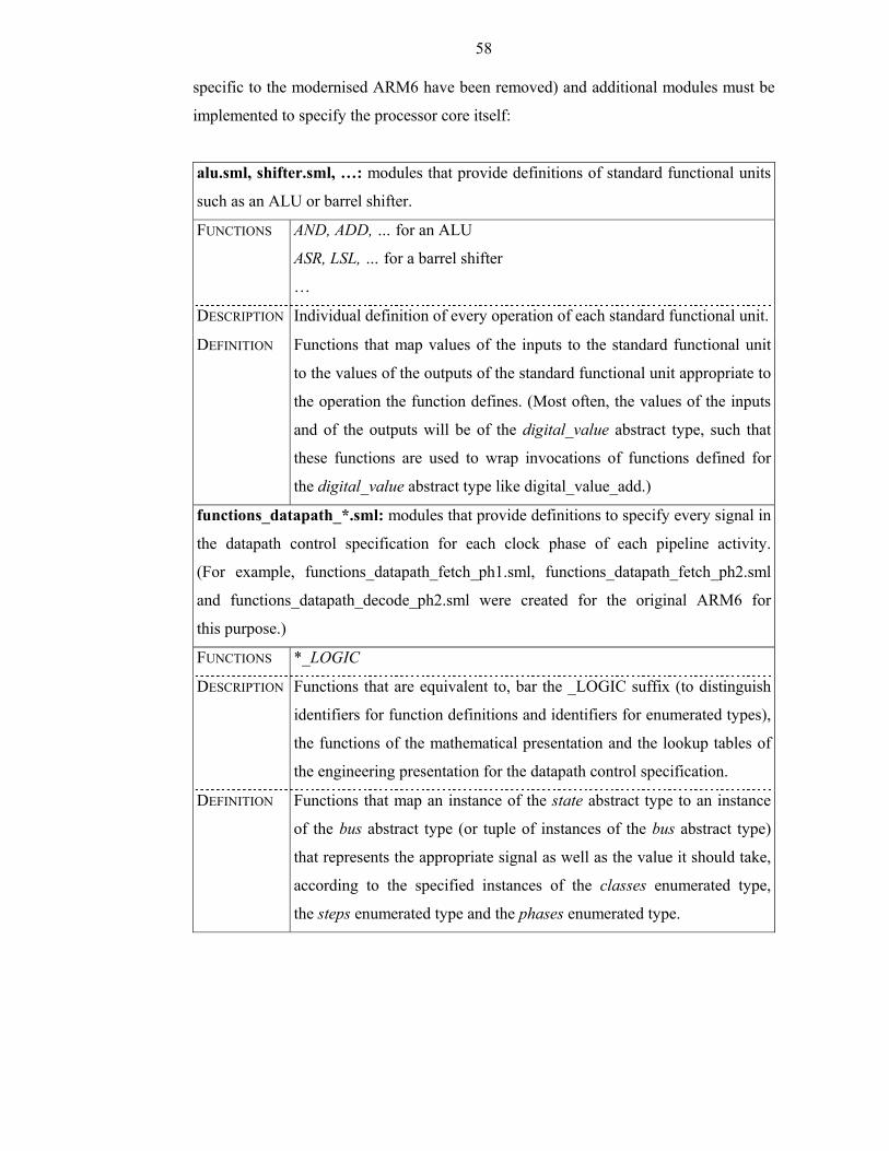
58
specific to the modernised ARM6 have been removed) and additional modules must be
implemented to specify the processor core itself:
alu.sml, shifter.sml, …: modules that provide definitions of standard functional units
such as an ALU or barrel shifter.
FUNCTIONS AND, ADD, … for an ALU
ASR, LSL, … for a barrel shifter
…
DESCRIPTION Individual definition of every operation of each standard functional unit.
DEFINITION Functions that map values of the inputs to the standard functional unit
to the values of the outputs of the standard functional unit appropriate to
the operation the function defines. (Most often, the values of the inputs
and of the outputs will be of the digital_value abstract type, such that
these functions are used to wrap invocations of functions defined for
the digital_value abstract type like digital_value_add.)
functions_datapath_*.sml: modules that provide definitions to specify every signal in
the datapath control specification for each clock phase of each pipeline activity.
(For example, functions_datapath_fetch_ph1.sml, functions_datapath_fetch_ph2.sml
and functions_datapath_decode_ph2.sml were created for the original ARM6 for
this purpose.)
FUNCTIONS *_LOGIC
DESCRIPTION Functions that are equivalent to, bar the _LOGIC suffix (to distinguish
identifiers for function definitions and identifiers for enumerated types),
the functions of the mathematical presentation and the lookup tables of
the engineering presentation for the datapath control specification.
DEFINITION Functions that map an instance of the state abstract type to an instance
of the bus abstract type (or tuple of instances of the bus abstract type)
that represents the appropriate signal as well as the value it should take,
according to the specified instances of the classes enumerated type,
the steps enumerated type and the phases enumerated type.
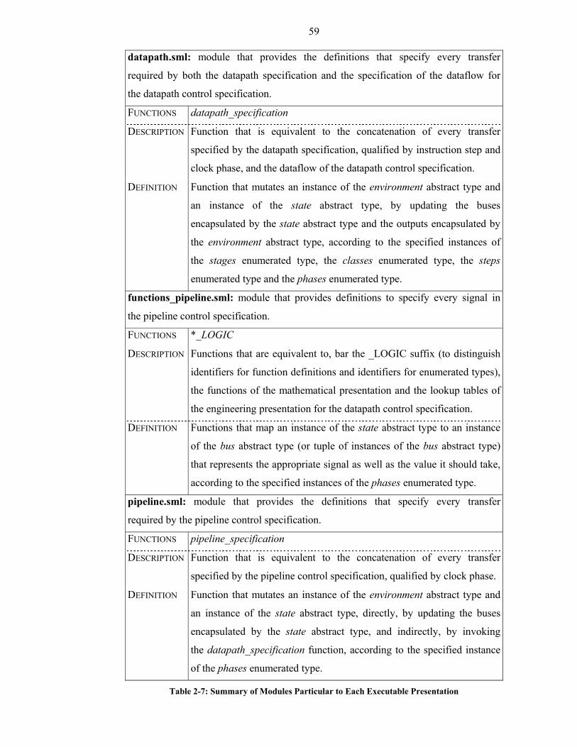
59
datapath.sml: module that provides the definitions that specify every transfer
required by both the datapath specification and the specification of the dataflow for
the datapath control specification.
FUNCTIONS datapath_specification
DESCRIPTION Function that is equivalent to the concatenation of every transfer
specified by the datapath specification, qualified by instruction step and
clock phase, and the dataflow of the datapath control specification.
DEFINITION Function that mutates an instance of the environment abstract type and
an instance of the state abstract type, by updating the buses
encapsulated by the state abstract type and the outputs encapsulated by
the environment abstract type, according to the specified instances of
the stages enumerated type, the classes enumerated type, the steps
enumerated type and the phases enumerated type.
functions_pipeline.sml: module that provides definitions to specify every signal in
the pipeline control specification.
FUNCTIONS *_LOGIC
DESCRIPTION Functions that are equivalent to, bar the _LOGIC suffix (to distinguish
identifiers for function definitions and identifiers for enumerated types),
the functions of the mathematical presentation and the lookup tables of
the engineering presentation for the datapath control specification.
DEFINITION Functions that map an instance of the state abstract type to an instance
of the bus abstract type (or tuple of instances of the bus abstract type)
that represents the appropriate signal as well as the value it should take,
according to the specified instances of the phases enumerated type.
pipeline.sml: module that provides the definitions that specify every transfer
required by the pipeline control specification.
FUNCTIONS pipeline_specification
DESCRIPTION Function that is equivalent to the concatenation of every transfer
specified by the pipeline control specification, qualified by clock phase.
DEFINITION Function that mutates an instance of the environment abstract type and
an instance of the state abstract type, directly, by updating the buses
encapsulated by the state abstract type, and indirectly, by invoking
the datapath_specification function, according to the specified instance
of the phases enumerated type.
Table 2-7: Summary of Modules Particular to Each Executable Presentation
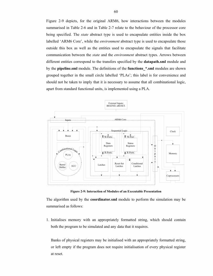
60
Figure 2-9 depicts, for the original ARM6, how interactions between the modules
summarised in Table 2-6 and in Table 2-7 relate to the behaviour of the processor core
being specified. The state abstract type is used to encapsulate entities inside the box
labelled ‘ARM6 Core’, while the environment abstract type is used to encapsulate those
outside this box as well as the entities used to encapsulate the signals that facilitate
communication between the state and the environment abstract types. Arrows between
different entities correspond to the transfers specified by the datapath.sml module and
by the pipeline.sml module. The definitions of the functions_*.sml modules are shown
grouped together in the small circle labelled ‘PLAs’; this label is for convenience and
should not be taken to imply that it is necessary to assume that all combinational logic,
apart from standard functional units, is implemented using a PLA.
StatusRegisters
DataRegisters
Latches ConditionalLatches
Reset-SetLatches
Sequential Logic
Combinational LogicPLAs
ALUBarrelShifter
Buses
ARM6 Core
External Inputs:BIGEND, nRESET.
Clock
Memory
Coprocessors
R-Ports R-Ports
W-Ports W-Port
Outputs
Inputs
Figure 2-9: Interaction of Modules of an Executable Presentation
The algorithm used by the coordinator.sml module to perform the simulation may be
summarised as follows:
1. Initialises memory with an appropriately formatted string, which should contain
both the program to be simulated and any data that it requires.
Banks of physical registers may be initialised with an appropriately formatted string,
or left empty if the program does not require initialisation of every physical register
at reset.
61
Environment events (which specify the value to be maintained for an external input,
until overridden by another environment event involving the same external input,
as soon as the specified number of clock cycles has elapsed), may be initialised from
an appropriately formatted string. Still the default constructor for the environment
abstract type should set up the minimum number of environment events required for
the processor core being specified to exit reset properly.
2. Invokes the environment_init_inputs function defined by the state.sml module.
a. Sets new CLK[*] (to appropriate identifier of phases enumerated type).
b. If now in first clock phase, checks whether any environment events are scheduled
for this clock cycle, and if some are, updates external inputs as appropriate.
3. Invokes the state_init_buses function defined by the state.sml module.
a. Resets all buses to the undefined value.
b. Resets state of the read ports and the write ports of each bank of physical registers
as appropriate for clock phase specified by CLK[*] and nature of port.
4. Invokes the pipeline_specification function defined by the pipeline.sml module
using the value of the CLK[*] input in the latest instance of the environment
abstract type as the current clock phase.
a. Invokes functions defined by the function_pipeline.sml module, as appropriate
for the current clock phase.
b. Invokes the datapath_specification function defined by the datapath.sml module,
for each pipeline stage that may dictate pipeline activities and which currently has
an instruction step associated with it (because of, depending on the pipeline stage,
the values of NXTIC[*] and NXTIS[*], IC[*] and IS[*] or buffered versions of
IC[*] and IS[*].) Each function invocation uses the latest instances of the state
and the environment abstract types.
i. Invokes environment_*_memory_read or environment_*_memory_write
(both of these functions are defined in the state.sml module), if memory access
completes in this clock phase.
ii. Invokes the state_update_buses function defined by the state.sml module,
which creates appropriate instances of the bus abstract type with the values of
the inputs in the instance of the environment abstract type.
iii. Invokes the functions defined by the function_datapath.sml module as needed
to derive particular instances of the bus abstract type with appropriate values,
using the state_insert_buses function defined by the state.sml module to add
these buses to the instance of the state abstract type. (Instances of the bus
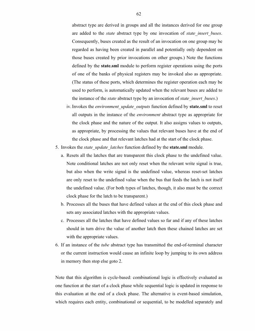
62
abstract type are derived in groups and all the instances derived for one group
are added to the state abstract type by one invocation of state_insert_buses.
Consequently, buses created as the result of an invocation on one group may be
regarded as having been created in parallel and potentially only dependent on
those buses created by prior invocations on other groups.) Note the functions
defined by the state.sml module to perform register operations using the ports
of one of the banks of physical registers may be invoked also as appropriate.
(The status of these ports, which determines the register operation each may be
used to perform, is automatically updated when the relevant buses are added to
the instance of the state abstract type by an invocation of state_insert_buses.)
iv. Invokes the environment_update_outputs function defined by state.sml to reset
all outputs in the instance of the environment abstract type as appropriate for
the clock phase and the nature of the output. It also assigns values to outputs,
as appropriate, by processing the values that relevant buses have at the end of
the clock phase and that relevant latches had at the start of the clock phase.
5. Invokes the state_update_latches function defined by the state.sml module.
a. Resets all the latches that are transparent this clock phase to the undefined value.
Note conditional latches are not only reset when the relevant write signal is true,
but also when the write signal is the undefined value, whereas reset-set latches
are only reset to the undefined value when the bus that feeds the latch is not itself
the undefined value. (For both types of latches, though, it also must be the correct
clock phase for the latch to be transparent.)
b. Processes all the buses that have defined values at the end of this clock phase and
sets any associated latches with the appropriate values.
c. Processes all the latches that have defined values so far and if any of these latches
should in turn drive the value of another latch then these chained latches are set
with the appropriate values.
6. If an instance of the tube abstract type has transmitted the end-of-terminal character
or the current instruction would cause an infinite loop by jumping to its own address
in memory then stop else goto 2.
Note that this algorithm is cycle-based: combinational logic is effectively evaluated as
one function at the start of a clock phase while sequential logic is updated in response to
this evaluation at the end of a clock phase. The alternative is event-based simulation,
which requires each entity, combinational or sequential, to be modelled separately and
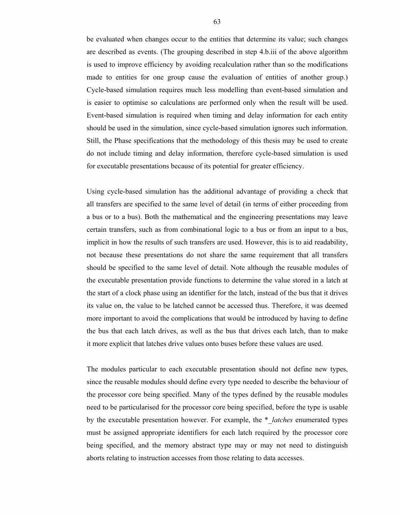
63
be evaluated when changes occur to the entities that determine its value; such changes
are described as events. (The grouping described in step 4.b.iii of the above algorithm
is used to improve efficiency by avoiding recalculation rather than so the modifications
made to entities for one group cause the evaluation of entities of another group.)
Cycle-based simulation requires much less modelling than event-based simulation and
is easier to optimise so calculations are performed only when the result will be used.
Event-based simulation is required when timing and delay information for each entity
should be used in the simulation, since cycle-based simulation ignores such information.
Still, the Phase specifications that the methodology of this thesis may be used to create
do not include timing and delay information, therefore cycle-based simulation is used
for executable presentations because of its potential for greater efficiency.
Using cycle-based simulation has the additional advantage of providing a check that
all transfers are specified to the same level of detail (in terms of either proceeding from
a bus or to a bus). Both the mathematical and the engineering presentations may leave
certain transfers, such as from combinational logic to a bus or from an input to a bus,
implicit in how the results of such transfers are used. However, this is to aid readability,
not because these presentations do not share the same requirement that all transfers
should be specified to the same level of detail. Note although the reusable modules of
the executable presentation provide functions to determine the value stored in a latch at
the start of a clock phase using an identifier for the latch, instead of the bus that it drives
its value on, the value to be latched cannot be accessed thus. Therefore, it was deemed
more important to avoid the complications that would be introduced by having to define
the bus that each latch drives, as well as the bus that drives each latch, than to make
it more explicit that latches drive values onto buses before these values are used.
The modules particular to each executable presentation should not define new types,
since the reusable modules should define every type needed to describe the behaviour of
the processor core being specified. Many of the types defined by the reusable modules
need to be particularised for the processor core being specified, before the type is usable
by the executable presentation however. For example, the *_latches enumerated types
must be assigned appropriate identifiers for each latch required by the processor core
being specified, and the memory abstract type may or may not need to distinguish
aborts relating to instruction accesses from those relating to data accesses.
64
fun NMREQ_LOGIC ic is PH1 state =
let
val O' = bus_digital_instance(NMREQ_BUS, digital_value_gen O [(BIT__0, BIT__0)]);
val I' = bus_digital_instance(NMREQ_BUS, digital_value_gen I [(BIT__0, BIT__0)]);
…
val nmulx_0' =
fn () => bus_digital_instance(NMREQ_BUS, digital_value_not( (state_lookup_digital_value_bus state MULX_BUS)
guard "invoked NMREQ_LOGIC before can use MULX bus" ));
in
case (ic, is)
of (DATA_PROC, T3) => O'
| (MRS_MSR, T3) => O'
| (REG_SHIFT, T3) => I'
| (REG_SHIFT, T4) => O'
| (MLA_MUL, T3) => I'
| (MLA_MUL, TN) => nmulx_0' ()
…
end
Figu
re 2
-10:
Exa
mpl
e *_
LO
GIC
Fun
ctio
n of
func
tions
_dat
apat
h_*.
sml M
odul
e
65
| datapath_specification DATA_PROC T3 PH2 environment state =
(* Fetch Datapath *)
let
val (environment', state') = (fn x => (x, state_update_buses state x))(environment_memory_read environment);
val state' = areg_block_dataflow environment' state' PH2;
val inc = (INC_LOGIC DATA_PROC T3 PH2 state')
guard "INC_LOGIC = NONE in datapath_specification DATA_PROC T3 PH2";
val state' = state_insert_buses state' [SOME inc];
(* Execute Datapath *)
val alu_logic = (ALU_LOGIC DATA_PROC T3 PH2 state')
guard "ALU_LOGIC = NONE in datapath_specification DATA_PROC T3 PH2");
val (alu, alunzcv) =
(fn (SOME alu, SOME alunzcv) => (alu, alunzcv)
| _ => error "… in datapath_specification DATA_PROC T3 PH2") alu_logic
val state' = state_insert_buses state' [SOME alu, SOME alunzcv];
…
in (environment', state')
end
Figu
re 2
-11:
Exa
mpl
e da
tapa
th_s
peci
ficat
ion
Func
tion
of D
atap
ath.
sml M
odul
e
66
None of the abstract types defined by the reusable modules expose the constructors
necessary for direct manipulation of the abstract type, thus the modules particular to
each executable presentation, and the reusable modules, must use the functions that
provide the interface for each abstract type. These functions are summarised along with
the relevant abstract type in the summaries of each reusable module in Appendix C.
Note modules particular to each executable presentation should mostly use functions
from state.sml and environment.sml as well as the functions to construct instances of
the bus abstract type. As may be seen by the cross-references within the summaries of
Appendix C, the other functions are defined mainly to be used by the reusable modules.
Figure 2-10 illustrates an example function of the functions_datapath_*.sml module.
Since most programming languages do not provide a straightforward method for
splitting up the definition of functions, as in the layout of the mathematical presentation,
the layout is based on that of the engineering presentation. The separate definitions of
one function for the mathematical presentation could have been combined into one that
used nested if then else expressions for the executable presentation, but this definition
would not be as clear or as readily understandable as that shown in Figure 2-10 due to
the complexity of the definitions that would be required. The let in end expression
defines appropriate bindings for the case of expression to enhance its resemblance to
the lookup table that would be defined by the engineering presentation (see Figure 2-8).
This facilitates comparisons between the engineering and the executable presentations,
required to ensure that the two presentations are equivalent.
Similarities between the datapath_specification function of the datapath.sml module
and the datapath specification of the mathematical presentation are less pronounced
than those between the functions of the executable and the engineering presentations.
Still, as shown in Figure 2-11, the datapath_specification function pattern matches on
the instruction class and the instruction step, each clause describing pipeline activities
associated with one pipeline stage (the Execute stage in the example of Figure 2-11).
This reflects how the mathematical presentation decomposes the datapath specification.
However, while the mathematical presentation treats all pipeline activities as separate,
the executable presentation uses comments to demarcate different pipeline activities
associated with the same pipeline stage. Both distinguish between pipeline activities
associated with one pipeline stage and those associated with different pipeline stages.
67
The datapath_specification function differs principally from the datapath specification
in terms of the timing with which the transfers are specified. As discussed above,
transfers to latches are not noted in datapath_specification, but are performed
automatically at the end of the clock phase. Furthermore, datapath_specification derives
instances of the bus abstract type in groups and adds instances to the state abstract type
by one invocation of the state_insert_buses function on these groups. This use of groups
provides more detail, about which buses may be driven in parallel and which depend on
values of other buses, than the mathematical presentation; which effectively handles
each transfer as being in a group by itself. (datapath_specification also makes explicit
the timing of the dataflow for the datapath control specification, by indicating when
local functions which specify this dataflow such as areg_block_dataflow are invoked;
the mathematical presentation leaves this implicit.)
Note the considerations discussed above for the functions_datapath_*.sml module
apply equally to the functions_pipeline_*.sml module, while those discussed above for
the datapath.sml module apply equally to the pipeline.sml module. In both instances,
the layout is the same for the two modules, but the interface by which the functions
are invoked is different (see Table 2-7).
Once the executable presentation has been created, the tube abstract type may be used
to output appropriate messages to stdout during simulation and thereby indicate whether
the simulation is progressing as expected. Nevertheless, this approach cannot provide
the detailed information that is often necessary to determine why the simulation failed
to progress as expected. Instead the trace abstract type may be used to trace the values
driven on buses at specified intervals during simulation. This internal representation
may be queried directly to discover the value driven on a bus at a specific point in time,
or it may be converted to a TDML representation using the trace_to_tdml_file function
and a text representation using the trace_to_text_file.
TDML or Timing Diagram Markup Language is an XML based standard for
representing waveform traces developed by Si2, which is documented at
http://www.si2.org/si2_publications/tdml/. TDML representations may be viewed in
waveform viewers that support this standard with results such as shown in Figure 2-12,
which was exported from TimingViewer for Microsoft Windows (developed by Forte
Design Systems).
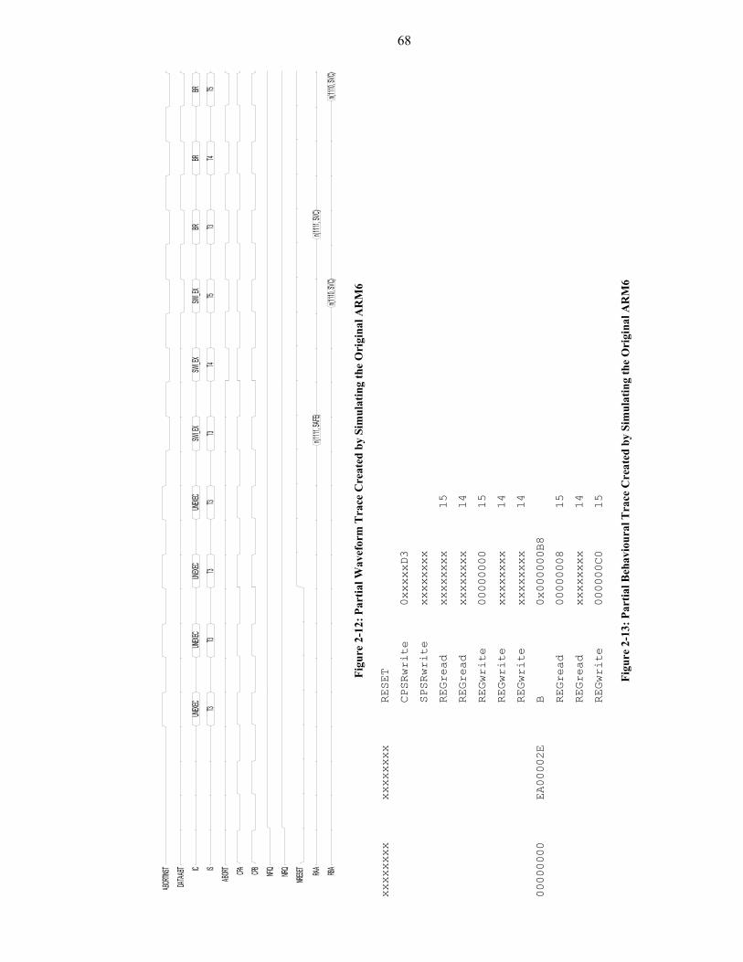
68
UNEXEC
UNEXEC
UNEXEC
UNEXEC
SWI_EX
SWI_EX
SWI_EX
BRBR
BRT3
T3T3
T3T3
T4T5
T3T4
T5
n(1111
,SAFE)
n(1111
,SVC)
n(1110
,SVC)
n(1110
,SVC)
ABORTI
NST
DATAA
BT IC IS
ABOR
T CPA CPB NFIQ NIRQ
NRESET RAA RBA
Figu
re 2
-12:
Par
tial W
avef
orm
Tra
ce C
reat
ed b
y Si
mul
atin
g th
e O
rigi
nal A
RM
6
xxxxxxxx
xxxxxxxx
RESET
CPSRwrite
0xxxxxD3
SPSRwrite
xxxxxxxx
REGread
xxxxxxxx
15
REGread
xxxxxxxx
14
REGwrite
00000000
15
REGwrite
xxxxxxxx
14
REGwrite
xxxxxxxx
14
00000000
EA00002E
B
0x000000B8
REGread
00000008
15
REGread
xxxxxxxx
14
REGwrite
000000C0
15
Figu
re 2
-13:
Par
tial B
ehav
iour
al T
race
Cre
ated
by
Sim
ulat
ing
the
Ori
gina
l AR
M6
69
The text representation, as illustrated in Figure 2-13, does not represent the values of
individual buses because this level of detail would make it difficult to understand.
Instead it summarises behaviour visible at the level of abstraction of the Programmer’s
Model specification, but as it occurs in the Phase specification so Figure 2-13 shows
multiple register writes to the same register for the RESET exception, since these occur
in different clock cycles as the exception iterates in the Execute stage (see Figure 4-1).
Note the format used for this text representation is similar to that used for the trace files
produced by Dominic Pajak’s ML simulator of his Programmer’s Model specification
of the ARM6, to facilitate comparison between simulations using his simulator and
simulations using the executable presentation of the original ARM6.
The trace abstract type does not maintain information about the values of latches, inputs
or outputs, since the values of these will be either driven on a bus or driven by a bus;
and the memory required to trace a simulation may be reduced by omitting information
about the values of these entities. Internally the trace abstract type divides all the buses
that may be driven in a clock phase into groups according to when and with which other
instances of the bus abstract type an instance of the bus abstract type will be added to
the state abstract type by one invocation of the state_insert_buses function. As noted in
the summary of the algorithm of the coordinator.sml module, the buses created from
one invocation may be regarded as having been created in parallel and potentially only
dependent on those buses created by prior invocations. The trace_to_tdml_file function
thus allows the time for which a value is driven on a bus in a clock phase to be scaled
such that the values of buses it may depend on are represented as being driven before
the value of the bus.
Since the trace abstract type was developed to help debug the executable presentation of
a formal specification, it is defined in terms of reference primitive types and array types
for efficiency and not in terms of more mathematically representable types. Types that
are more mathematically representable require instances of abstract types to be modified
by creating a new instance from the current instance that includes the changes.
Although the automatic garbage collection provided by the Standard ML interpreter
should ensure the memory allocated to old instances is freed up when the old instance
is no longer required, reference primitive types and array types significantly improve
the speed with which the values driven on buses may be traced. The trace abstract type
maintains information on the values driven on buses in arrays of arrays with:
70
1. A root array for each clock phase, which is a dynamically resizable array of
2. an array of pages similar to that created for the memory abstract type, but indexed by
the clock cycle at which the value of a bus is traced. Each page is an array of
3. an array of timing groups indexed by the ordinal number of the invocation of
state_insert_buses on the group of buses in which an instance of the bus abstract type
was added to the state abstract type such that the value of the relevant bus is traced.
Each timing group is an array of
4. an array of trace elements indexed by the ordinal number of the bus when the group,
in which it is added as an instance of the bus abstract type by an invocation of
state_insert_buses such that the value of the bus is traced, is alphabetically sorted.
Each trace element is an optional union type of all the possible types of bus values.
Note that the use of root arrays of pages improves the efficiency of tracing values
driven on buses for non-continuous intervals of clock cycles as well as for intervals that
start significantly after simulation itself began, since no page needs to be instantiated
unless it is referred to one or more clock cycles for which trace information is required.
2.4 Comparison of Presentations
The mathematical and the engineering presentations present the datapath specification,
and the specification of dataflow, in identical fashion using sequences of transfers.
Although the executable presentation uses explicit sequences of transfers to buses in
the datapath_specification function, transfers to latches are implicit in how functions of
the reusable modules are particularised to the processor core being specified, rather than
explicit in the functions particular to the executable presentation of the processor core.
Despite this, because the datapath_specification function pattern matches on
instruction step, not just clock phase, the similarity between the sequences of transfers
specified by the datapath_specification function of the executable presentation and
those specified by the datapath specification of the other presentations is pronounced.
The datapath_specification function would be more efficient if it pattern matched on
clock phase only and specified the set of transfers that any instruction step might require
in each clock phase, but only by significantly diminishing the correspondence between
the executable presentation and the other presentations.
The layout of the mathematical presentation of the datapath control specification with
functions split across instruction steps, allows dependencies in the evaluation of logic
71
to be clearly specified by the order in which each instruction step presents functions.
However, the engineering and the executable presentations are probably more useful for
understanding the individual nature of each entity of combinational logic, since both of
these presentations detail the behaviour of each entity using one definition. (Note that
the engineering presentation uses one definition for each clock phase in which the value
driven by the combinational logic is valid. In general, this is only one clock phase and
one definition, but even when it is not, the number of definitions needed is still less than
for mathematical presentations.) Mathematical presentations could be created to specify
combinational logic with the same number of definitions as engineering presentations,
but would be harder to maintain and to understand as a consequence, because functions
do not scale so straightforwardly with the size of the definition as lookup tables (or case
of expressions).
In certain respects, the engineering presentation may be viewed as intermediate between
the mathematical and the executable presentations. Its datapath specification is identical
to the mathematical presentation, its datapath control and pipeline control specifications
use lookup tables similar to the case of expressions of the executable presentation.
Transformation from lookup tables to case of expressions is fairly straightforward and
could be automated by a suitable ‘parser’ and ‘compiler’. However, transformation of
transfers from the datapath specifications of mathematical and engineering presentations
is more problematic, since the order of transfers not shared between the specifications of
every instruction would have to be determined. (Note that the engineering presentation
is useful in itself, apart from as an intermediate, since unlike an executable presentation
it is not limited by being written in one programming language rather than another.)
In terms of formal verification (Fox 2002), the concept of the explicit definition of
control signals in the datapath control and the pipeline control specifications facilitated
more detailed modelling of the Hardware Implementation specification as intended.
Furthermore, the treatment of instruction classes and instruction steps developed for
the methodology of this thesis was for the most part adopted, and proved useful in
showing how the proof could be decomposed. Yet contrary to the recommendations of
this section, Fox (2002) modified the specification of the ARM6 discussed in section 4
so the datapath control and the pipeline control specifications used unitary definitions of
mathematical functions and the equivalent of a unitary datapath_specification function
merged with a pipeline_specification function. These modifications were undertaken
72
to reduce the number of cases that had to be considered in order to prove correctness for
each instruction class and in conjunction with various other simplifications to facilitate
the initial verification attempt. Moreover, some of these modifications would be needed
to create one presentation from another. Hence, that such modifications were made
demonstrates the need for the flexibility which incorporation of three presentations into
the methodology of this thesis provides rather than that the methodology of thesis is not
flexible enough.
2.5 Summary
Tahar and Kumar (1998) provided the inspiration for much of the first attempt at
developing the mathematical presentation of the datapath specification (see section 4.2).
Nonetheless, significant additions and modifications were made to ensure the aims that
this methodology was developed to meet were met:
1. Development of datapath control specification and pipeline control specification
for the specification of control logic.
2. Subdivision of the Phase specification to facilitate addition of the datapath control
and the pipeline control specifications to create complete specification of
implementation of processor core.
3. Use of executable layout rather than structural layout.
4. Division of instruction classes into instruction steps.
5. Explicit distinction between pipeline activities and pipeline stages in specification.
6. Development of explicit syntax for the mathematical presentation.
7. Introduction of timing annotation.
8. Concept of optional transfers and optional pipeline activities, which occur only on
certain instantiations of the relevant instruction class.
9. Addition of engineering presentation and executable presentation.
10. Use of explicit notation for buffering of buses by pipeline latches.
(The history behind these changes is documented in section 4, and to a lesser extent in
section 6; section 2.3 presents the general methodology that was developed as a result of
making these additions and modifications.)
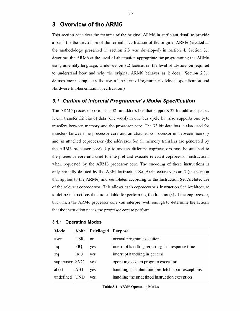
73
3 Overview of the ARM6 This section considers the features of the original ARM6 in sufficient detail to provide
a basis for the discussion of the formal specification of the original ARM6 (created as
the methodology presented in section 2.3 was developed) in section 4. Section 3.1
describes the ARM6 at the level of abstraction appropriate for programming the ARM6
using assembly language, while section 3.2 focuses on the level of abstraction required
to understand how and why the original ARM6 behaves as it does. (Section 2.2.1
defines more completely the use of the terms Programmer’s Model specification and
Hardware Implementation specification.)
3.1 Outline of Informal Programmer’s Model Specification
The ARM6 processor core has a 32-bit address bus that supports 32-bit address spaces.
It can transfer 32 bits of data (one word) in one bus cycle but also supports one byte
transfers between memory and the processor core. The 32-bit data bus is also used for
transfers between the processor core and an attached coprocessor or between memory
and an attached coprocessor (the addresses for all memory transfers are generated by
the ARM6 processor core). Up to sixteen different coprocessors may be attached to
the processor core and used to interpret and execute relevant coprocessor instructions
when requested by the ARM6 processor core. The encoding of these instructions is
only partially defined by the ARM Instruction Set Architecture version 3 (the version
that applies to the ARM6) and completed according to the Instruction Set Architecture
of the relevant coprocessor. This allows each coprocessor’s Instruction Set Architecture
to define instructions that are suitable for performing the function(s) of the coprocessor,
but which the ARM6 processor core can interpret well enough to determine the actions
that the instruction needs the processor core to perform.
3.1.1 Operating Modes
Mode Abbr. Privileged Purpose
user USR no normal program execution
fiq FIQ yes interrupt handling requiring fast response time
irq IRQ yes interrupt handling in general
supervisor SVC yes operating system program execution
abort ABT yes handling data abort and pre-fetch abort exceptions
undefined UND yes handling the undefined instruction exception
Table 3-1: ARM6 Operating Modes
74
The six operating modes supported by the ARM6 processor core are summarised in
Table 3-1.
3.1.2 Exceptions
The following seven exceptions may be raised on the ARM6 processor core:
1. RESET: occurs when the nRESET input to the processor core is deasserted after being
taken LOW and is used to initialise the ARM6 processor core when first powered up.
2. DATA ABORT: occurs when the processor core executes an instruction that tries to
read from or write to an illegal address (an address that is deemed inaccessible in
the processor core’s current operating mode by the memory management subsystem.)
3. FAST INTERRUPT REQUEST: occurs when the processor core detects the nFIQ input
asserted LOW before executing its next instruction and when this type of interrupt
is not masked out.
4. INTERRUPT REQUEST: occurs when the processor core detects the nIRQ input
asserted LOW before executing its next instruction and when this type of interrupt
is not masked out.
5. PRE-FETCH ABORT: occurs when the processor core attempts to execute an instruction
pre-fetched from an illegal address (see 2 above).
6. SOFTWARE INTERRUPT: occurs when the processor core executes the SWI instruction.
7. UNDEFINED INSTRUCTION TRAP: occurs when the processor core attempts to execute
coprocessor instructions not recognised by an attached coprocessor or an instruction
that is defined as UNDEFINED by the ARM Instruction Set Architecture version 3.
(This allows software emulation of coprocessor instructions, or of future extensions
to the ARM Instruction Set Architecture that redefine instructions currently defined
as UNDEFINED, by writing an appropriate exception handler.)
All seven exceptions cause the processor core to restart instruction pre-fetching from
an address (exception vector) and enter an apposite operating mode (see section 3.1.1).
Fast interrupt requests are masked out by the reset and fast interrupt request exceptions,
while all exceptions mask out interrupt requests. In addition, all but the reset exception
require the processor core to store program status information and the return address
such that program execution can be resumed after the exception has been handled.
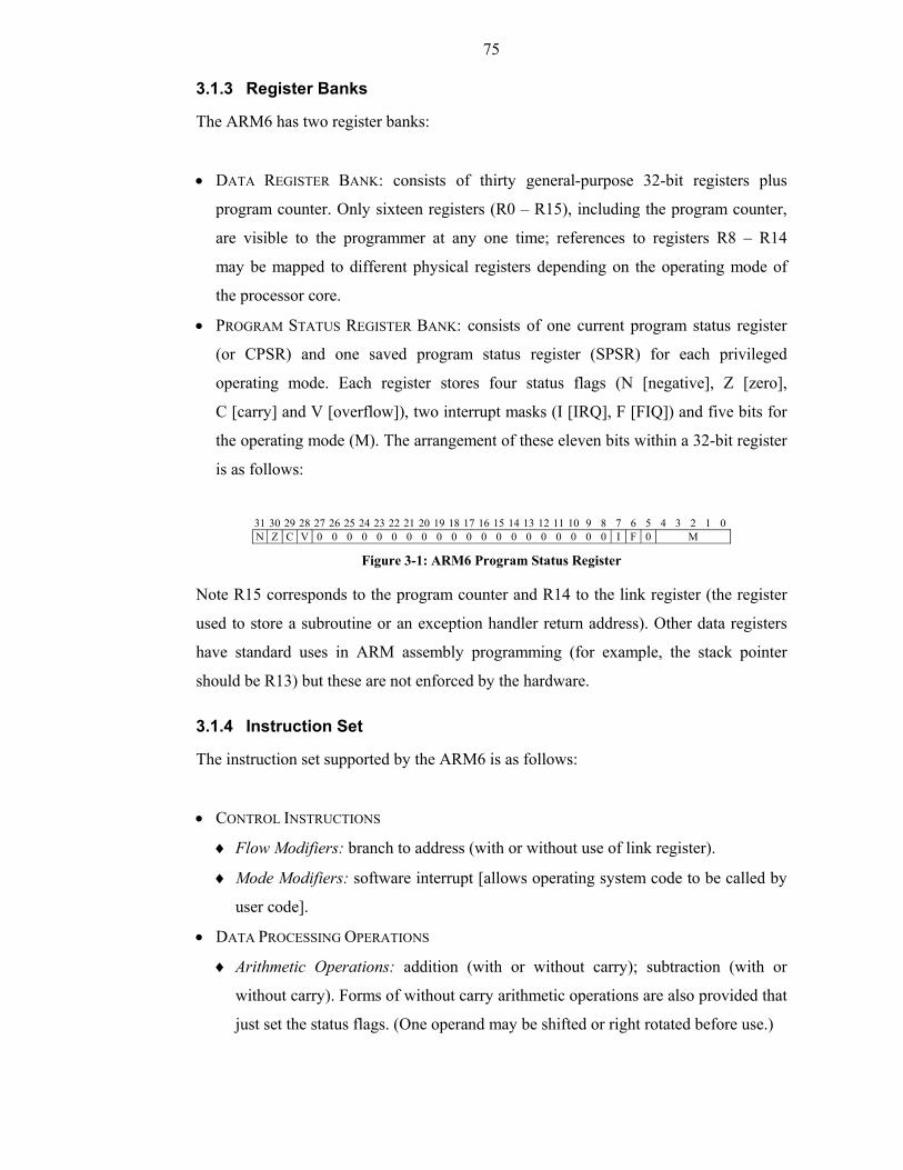
75
3.1.3 Register Banks
The ARM6 has two register banks:
• DATA REGISTER BANK: consists of thirty general-purpose 32-bit registers plus
program counter. Only sixteen registers (R0 – R15), including the program counter,
are visible to the programmer at any one time; references to registers R8 – R14
may be mapped to different physical registers depending on the operating mode of
the processor core.
• PROGRAM STATUS REGISTER BANK: consists of one current program status register
(or CPSR) and one saved program status register (SPSR) for each privileged
operating mode. Each register stores four status flags (N [negative], Z [zero],
C [carry] and V [overflow]), two interrupt masks (I [IRQ], F [FIQ]) and five bits for
the operating mode (M). The arrangement of these eleven bits within a 32-bit register
is as follows:
31 30 29 28 27 26 25 24 23 22 21 20 19 18 17 16 15 14 13 12 11 10 9 8 7 6 5 4 3 2 1 0 N Z C V 0 0 0 0 0 0 0 0 0 0 0 0 0 0 0 0 0 0 0 0 I F 0 M
Figure 3-1: ARM6 Program Status Register
Note R15 corresponds to the program counter and R14 to the link register (the register
used to store a subroutine or an exception handler return address). Other data registers
have standard uses in ARM assembly programming (for example, the stack pointer
should be R13) but these are not enforced by the hardware.
3.1.4 Instruction Set
The instruction set supported by the ARM6 is as follows:
• CONTROL INSTRUCTIONS
♦ Flow Modifiers: branch to address (with or without use of link register).
♦ Mode Modifiers: software interrupt [allows operating system code to be called by
user code].
• DATA PROCESSING OPERATIONS
♦ Arithmetic Operations: addition (with or without carry); subtraction (with or
without carry). Forms of without carry arithmetic operations are also provided that
just set the status flags. (One operand may be shifted or right rotated before use.)
76
♦ Logical Operations: and; exclusive or; inclusive or; bit clear [and not]. Forms of
the first two are also provided that just set the CPSR status flags. (One operand
may be shifted or right rotated before use.)
♦ Multiplication Operations: 32-bit multiplication (with or without addition of
initial value).
♦ Transfer Operations: move value (with or without negation) to some data register
(the value may be also shifted or right rotated before use); move value to
program status register; move value from program status register to data register.
• MEMORY INSTRUCTIONS
♦ Single Data Transfer: load data register (word or unsigned byte) from memory;
store value (word or byte) to memory.
♦ Block Data Transfer: load non-empty subset of the data registers with
consecutively located words from memory (if in privileged mode may be used
to change mode if the program counter is loaded or to load user bank registers
if not loaded); store words from non-empty subset of the data registers to
consecutive memory locations (if in privileged mode may be used to store values
from user bank registers).
♦ Semaphore Instruction: load data register then store data register (using word or
unsigned byte values) at same memory location. [Source and destination register
may be the same]
• COPROCESSOR INSTRUCTIONS [if not supported by any coprocessor in the system
being considered then these behave as the Undefined Instruction described below.]
♦ Data Operation: cause coprocessor to perform coprocessor defined operation.
♦ Data Transfer: provide values of successive memory locations to coprocessor;
store values provided by coprocessor to successive memory locations.
♦ Register Transfer: load data register with the value provided by coprocessor;
transfer value from processor core to coprocessor.
• INSTRUCTION SET EXTENDERS
♦ Undefined Instruction: cause an undefined exception.
Note that all instructions are conditionally executed; fifteen different condition codes
may be used (including ‘always execute’) and an instruction will execute if and only if
its four bit condition code is met by the CPSR status flags.
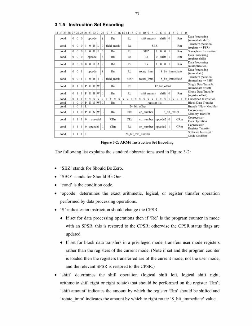
77
3.1.5 Instruction Set Encoding 31 30 29 28 27 26 25 24 23 22 21 20 19 18 17 16 15 14 13 12 11 10 9 8 7 6 5 4 3 2 1 0
cond 0 0 0 opcode S Rn Rd shift amount shift 0 Rm Data Processing (immediate shift)
cond 0 0 0 1 0 R L 0 field_mask Rd SBZ Rm Transfer Operation (register ↔ PSR)
cond 0 0 0 1 0 B 0 0 Rn Rd SBZ 1 0 0 1 Rm Semaphore Instruction
cond 0 0 0 opcode S Rn Rd Rs 0 shift 1 Rm Data Processing (register shift)
cond 0 0 0 0 0 0 A S Rd Rn Rs 1 0 0 1 Rm Data Processing (multiplication)
cond 0 0 1 opcode S Rn Rd rotate_imm 8_bit_immediate Data Processing (immediate)
cond 0 0 1 1 0 R 1 0 field_mask SBO rotate_imm 8_bit_immediate Transfer Operation (immediate → PSR)
cond 0 1 0 P U B W L Rn Rd 12_bit_offset Single Data Transfer (immediate offset)
cond 0 1 1 P U B W L Rn Rd shift amount shift 0 Rm Single Data Transfer (register offset)
cond 0 1 1 x x x x x x x x x x x x x x x x x x x x 1 x x x x Undefined Instruction cond 1 0 0 P U S W L Rn register list Block Data Transfer cond 1 0 1 L 24_bit_offset Branch / Flow Modifier
cond 1 1 0 P U N W L Rn CRd cp_number 8_bit_offset Coprocessor Memory Transfer
cond 1 1 1 0 opcode1 CRn CRd cp_number opcode2 0 CRm Coprocessor Data Operation
cond 1 1 1 0 opcode1 L CRn Rd cp_number opcode2 1 CRm Coprocessor Register Transfer
cond 1 1 1 1 24_bit_swi_number Software Interrupt / Mode Modifier
Figure 3-2: ARM6 Instruction Set Encoding
The following list explains the standard abbreviations used in Figure 3-2:
• ‘SBZ’ stands for Should Be Zero.
• ‘SBO’ stands for Should Be One.
• ‘cond’ is the condition code.
• ‘opcode’ determines the exact arithmetic, logical, or register transfer operation
performed by data processing operations.
• ‘S’ indicates an instruction should change the CPSR.
♦ If set for data processing operations then if ‘Rd’ is the program counter in mode
with an SPSR, this is restored to the CPSR; otherwise the CPSR status flags are
updated.
♦ If set for block data transfers in a privileged mode, transfers user mode registers
rather than the registers of the current mode. (Note if set and the program counter
is loaded then the registers transferred are of the current mode, not the user mode,
and the relevant SPSR is restored to the CPSR.)
• ‘shift’ determines the shift operation (logical shift left, logical shift right,
arithmetic shift right or right rotate) that should be performed on the register ‘Rm’;
‘shift amount’ indicates the amount by which the register ‘Rm’ should be shifted and
‘rotate_imm’ indicates the amount by which to right rotate ‘8_bit_immediate’ value.
78
• If ‘R’ = 0 the PSR transfer should involve the CPSR and if ‘R’ = 1 the SPSR.
• ‘field_mask’ indicates which of the four bytes of the CPSR or relevant SPSR
should be updated when considered as 32-bit registers.
♦ If transfer operation Register ← PSR then ‘field_mask’ SBO.
• ‘L’ indicates the direction of transfer instructions.
♦ If memory transfer then ‘L’ = 0 indicates register (coprocessor) → memory and
‘L’ = 1 register (coprocessor) ← memory.
♦ If PSR transfer then ‘L’ = 0 indicates register ← PSR and ‘L’ = 1 register → PSR.
♦ If coprocessor register transfer then ‘L’ = 0 indicates register → coprocessor and
‘L’ = 1 indicates register ← coprocessor.
• ‘L’ when set for branches indicates that the link register should be updated.
• ‘A’ when set indicates that some value should be added to the multiplication result.
• ‘register list’ has bits corresponding to each data register (bit 0 ⇒ R0, bit 1 ⇒ R1
and so forth), which when set indicate the corresponding register should be used in
the block data transfer.
• ‘Rd’ is the destination register.
♦ If transfer operation Register → PSR then ‘Rd’ SBO.
♦ If data processing that only sets the status flags then ‘Rd’ SBZ.
• ‘Rn’, ‘Rm’ and ‘Rs’ are source registers.
♦ If transfer operation Register → PSR then ‘Rm’ SBZ.
♦ If multiplication operation and ‘A’ = 0 then ‘Rn’ SBZ.
• ‘B’ = 0 indicates word memory transfer and ‘B’ = 1 indicates byte memory transfer.
• ‘U’ = 0 indicates offset is subtracted from the base address (and block data transfer
should proceed downwards) while ‘U’ = 1 indicates offset is added to base address
(and block data transfer should proceed upwards).
• ‘P’ and ‘W’ determine the various addressing modes of memory transfer instructions.
♦ For single data transfer operations:
‘P’ = 0 indicates use of post-indexed addressing (the base address is modified by
the offset after memory access). Since writeback is assumed, in a privileged mode
‘W’ = 1 indicates memory access should be treated as if non-privileged.
‘P’ = 1 indicates use of pre-indexed addressing (the base address is modified by
the offset before memory access) with writeback only if ‘W’ = 1
79
♦ For block data transfer operations:
‘P’ = 0 indicates that the memory locations accessed should include the word at
the base address and ‘P’ = 1 indicates that the word should be excluded.
‘W’ = 1 indicates that the register used for the base address should be updated
after transfer and ‘W’ = 0 indicates that it should not.
♦ For coprocessor memory transfers:
‘P’ = 0 indicates use of post-indexed addressing with writeback only if ‘W’ = 1.
‘P’ = 1 indicates use of pre-indexed addressing with writeback only if ‘W’ = 1.
• ‘cp_number’ is the number of the coprocessor that should execute the instruction.
• ‘opcode1’ and ‘opcode2’ are the fields that the ARM Instruction Set Architecture
version 3 suggests should encode the opcode of coprocessor instructions.
• ‘CRd’ is the field that the ARM Instruction Set Architecture version 3 suggests
should encode the destination register for coprocessor instructions.
• ‘CRm’ and ‘CRn’ are fields the ARM Instruction Set Architecture version 3 suggests
should encode the source registers for coprocessor instructions.
• ‘N’ is the bit the ARM Instruction Set Architecture version 3 suggests should encode
memory transfer length for coprocessor instructions.
3.2 Outline of Informal Hardware Implementation Specification
The ARM6 processor core memory interface conforms to the von Neumann architecture
in assuming that it connects one read-write memory to the ARM6 processor core,
which contains all instructions and all data. (This assumption still applies even when
the ARM6 processor core memory interface is connected indirectly to main memory via
a cache and a write buffer like in the ARM610. The Memory Management Unit that
controls the operation of such components interacts with the ARM6 processor core as
a coprocessor—also with the abort signal, see below—such that the memory interface
may still treat the connection to main memory as direct.)
3.2.1 Signal Description
The ARM6 processor core can use the address bus ADDR and the two data buses
DIN (Data IN) and DOUT (Data OUT) to make one of four different types of transfer
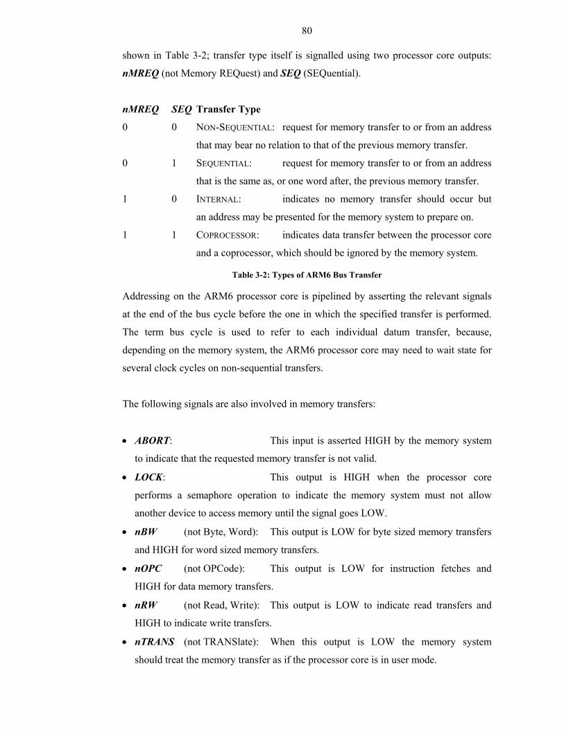
80
shown in Table 3-2; transfer type itself is signalled using two processor core outputs:
nMREQ (not Memory REQuest) and SEQ (SEQuential).
nMREQ SEQ Transfer Type
0 0 NON-SEQUENTIAL: request for memory transfer to or from an address
that may bear no relation to that of the previous memory transfer.
0 1 SEQUENTIAL: request for memory transfer to or from an address
that is the same as, or one word after, the previous memory transfer.
1 0 INTERNAL: indicates no memory transfer should occur but
an address may be presented for the memory system to prepare on.
1 1 COPROCESSOR: indicates data transfer between the processor core
and a coprocessor, which should be ignored by the memory system.
Table 3-2: Types of ARM6 Bus Transfer
Addressing on the ARM6 processor core is pipelined by asserting the relevant signals
at the end of the bus cycle before the one in which the specified transfer is performed.
The term bus cycle is used to refer to each individual datum transfer, because,
depending on the memory system, the ARM6 processor core may need to wait state for
several clock cycles on non-sequential transfers.
The following signals are also involved in memory transfers:
• ABORT: This input is asserted HIGH by the memory system
to indicate that the requested memory transfer is not valid.
• LOCK: This output is HIGH when the processor core
performs a semaphore operation to indicate the memory system must not allow
another device to access memory until the signal goes LOW.
• nBW (not Byte, Word): This output is LOW for byte sized memory transfers
and HIGH for word sized memory transfers.
• nOPC (not OPCode): This output is LOW for instruction fetches and
HIGH for data memory transfers.
• nRW (not Read, Write): This output is LOW to indicate read transfers and
HIGH to indicate write transfers.
• nTRANS (not TRANSlate): When this output is LOW the memory system
should treat the memory transfer as if the processor core is in user mode.
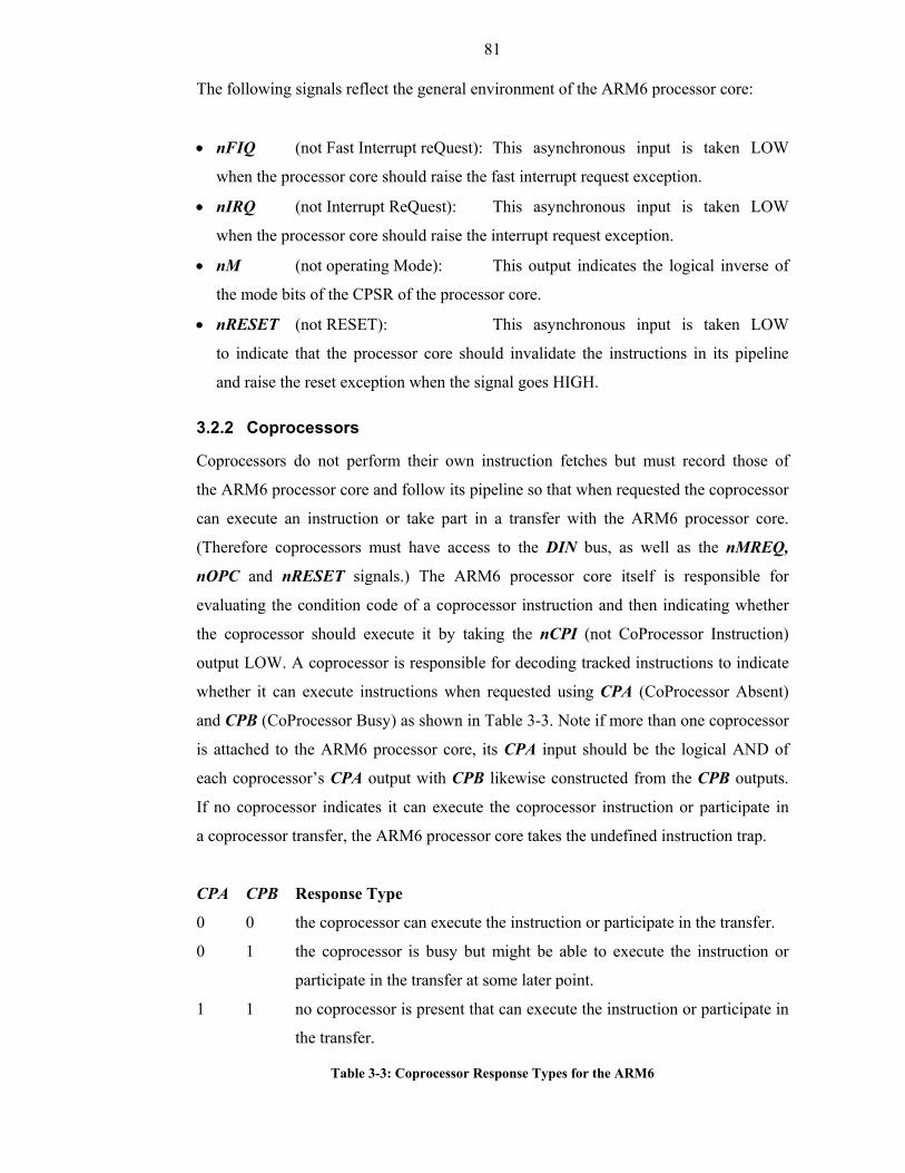
81
The following signals reflect the general environment of the ARM6 processor core:
• nFIQ (not Fast Interrupt reQuest): This asynchronous input is taken LOW
when the processor core should raise the fast interrupt request exception.
• nIRQ (not Interrupt ReQuest): This asynchronous input is taken LOW
when the processor core should raise the interrupt request exception.
• nM (not operating Mode): This output indicates the logical inverse of
the mode bits of the CPSR of the processor core.
• nRESET (not RESET): This asynchronous input is taken LOW
to indicate that the processor core should invalidate the instructions in its pipeline
and raise the reset exception when the signal goes HIGH.
3.2.2 Coprocessors
Coprocessors do not perform their own instruction fetches but must record those of
the ARM6 processor core and follow its pipeline so that when requested the coprocessor
can execute an instruction or take part in a transfer with the ARM6 processor core.
(Therefore coprocessors must have access to the DIN bus, as well as the nMREQ,
nOPC and nRESET signals.) The ARM6 processor core itself is responsible for
evaluating the condition code of a coprocessor instruction and then indicating whether
the coprocessor should execute it by taking the nCPI (not CoProcessor Instruction)
output LOW. A coprocessor is responsible for decoding tracked instructions to indicate
whether it can execute instructions when requested using CPA (CoProcessor Absent)
and CPB (CoProcessor Busy) as shown in Table 3-3. Note if more than one coprocessor
is attached to the ARM6 processor core, its CPA input should be the logical AND of
each coprocessor’s CPA output with CPB likewise constructed from the CPB outputs.
If no coprocessor indicates it can execute the coprocessor instruction or participate in
a coprocessor transfer, the ARM6 processor core takes the undefined instruction trap.
CPA CPB Response Type
0 0 the coprocessor can execute the instruction or participate in the transfer.
0 1 the coprocessor is busy but might be able to execute the instruction or
participate in the transfer at some later point.
1 1 no coprocessor is present that can execute the instruction or participate in
the transfer.
Table 3-3: Coprocessor Response Types for the ARM6
82
Handshaking between the ARM6 processor core and coprocessors occurs as follows:
1. If the instruction in the Decode stage of each coprocessor is a coprocessor instruction
or requests a coprocessor transfer, then each coprocessor drives its CPA output and
its CPB output appropriately.
2. If a coprocessor instruction enters the Execute stage of the ARM6 processor core or
an instruction that requests a coprocessor transfer, and it passes its condition code,
the ARM6 processor core takes nCPI LOW to indicate that the relevant coprocessor
may start executing the instruction or making the transfer. The ARM6 processor core
busy-waits while CPB is asserted if CPA was deasserted and CPB asserted at 1.
However if an interrupt occurs then the ARM6 processor core will deassert nCPI and
serve the interrupt (assuming that the interrupt was not masked out by the CPSR),
whereas if the coprocessor reasserts CPA, the undefined instruction trap exception
will be taken.
3. If a coprocessor memory transfer is being performed then the ARM6 processor core
should stop supplying addresses for the transfer when the coprocessor deasserts both
CPA and CPB.
3.2.3 Datapath of Processor Core
The datapath of the ARM6 processor core may be depicted as shown in Figure 3-3.
Buses are depicted using arrows and the relationship between buses and the components
it connects may be determined by the direction of approach:
• Arrows from the left and from below denote inputs to the connected component.
(Note arrows from below are used instead of arrows from the left as needed to make
the diagram clearer.)
• Arrows from the right denote outputs from the connected component.
• Arrows from the top denote signals that control the operation of the component:
which function should be performed by combinational logic; condition under which
a static latch should be transparent; or whether a register port should transfer data,
and if it should, which register the data should be transferred to or from.
Buses that connect to components in the control subsystem of the ARM6 processor core
are depicted as terminating at or beginning with the name of the relevant control block;
for clarity, these connections are depicted orthogonal to those concerned solely with
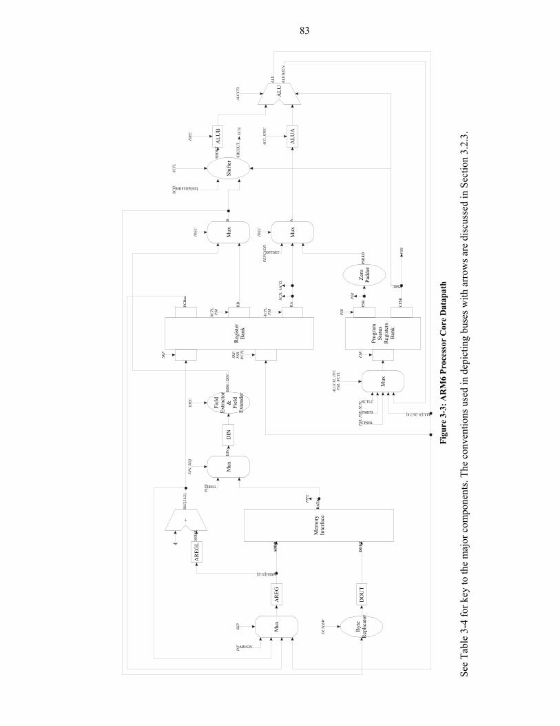
83
Figu
re 3
-3: A
RM
6 Pr
oces
sor
Cor
e D
atap
ath
See
Tabl
e 3-
4 fo
r key
to th
e m
ajor
com
pone
nts.
The
conv
entio
ns u
sed
in d
epic
ting
buse
s with
arr
ows a
re d
iscu
ssed
in S
ectio
n 3.
2.3.
Reg
ister
Ban
k
Prog
ram
Stat
usR
egis
ters
Ban
k
Mux
Mux
ALU
Shift
er
ALU
RA
RB
PCB
usIN
C[3
1:2]
+
4
AR
EG
DO
UT
AD
DR
Mux
Mem
ory
Inte
rfac
e
Byte
Rep
licat
or
ACTL
,PS
R
BCTL
,PS
R
Zero
Padd
er
PSR
ALU
B
SCTL
MC
TL
AA
LUA
SCTL
SKP
SKP,
PSR,
WC
TL
PEN
CAD
D
SHIFTOP[4:0]
SHO
UT
ALU
, ID
EC
IDEC
ALU
CTL
ALU
CTL
, IN
T,PS
R, W
CTL
PSR
ALU
NZC
V
ALU[31:26,7:0]
SCTLC
PSRFB
CPSRLPSR,
PSR
, SC
TL
SCTL
PSR
PSR
PSR
RD
PSR
SHC
OU
T
IDEC
IDEC
B
IREG
DA
TAPIPE
PIPE
Mux
DIN
, SEQ
DIN
Fiel
dEx
tract
or& Fiel
dEx
tend
er
DIN
IMM
/ D
IN’
IDEC
AREG[31:2]
AR
EGL
AR
EGL
AREGN
INT
SKP
DC
TLBW
CPS
R
Mux
PSRC
OFFSET
DO
UT
SCTL
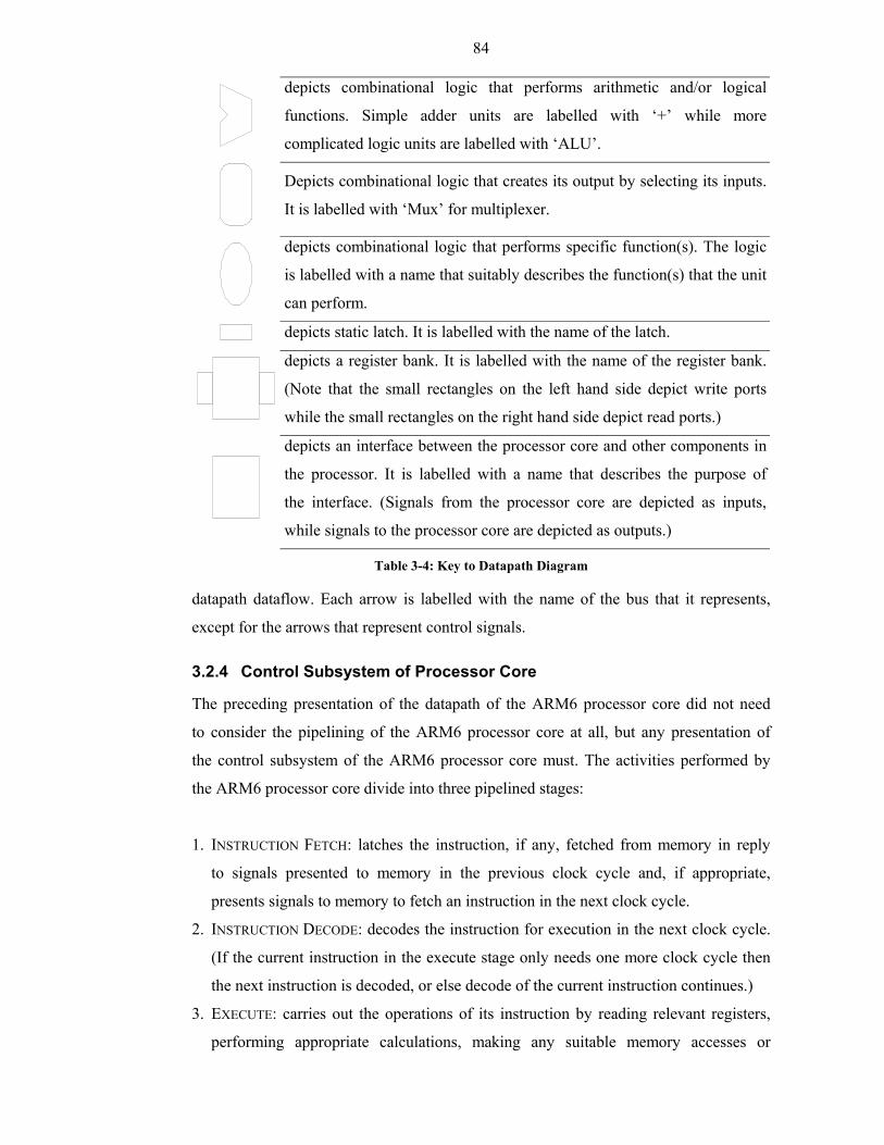
84
depicts combinational logic that performs arithmetic and/or logical
functions. Simple adder units are labelled with ‘+’ while more
complicated logic units are labelled with ‘ALU’.
Depicts combinational logic that creates its output by selecting its inputs.
It is labelled with ‘Mux’ for multiplexer.
depicts combinational logic that performs specific function(s). The logic
is labelled with a name that suitably describes the function(s) that the unit
can perform.
depicts static latch. It is labelled with the name of the latch.
depicts a register bank. It is labelled with the name of the register bank.
(Note that the small rectangles on the left hand side depict write ports
while the small rectangles on the right hand side depict read ports.)
depicts an interface between the processor core and other components in
the processor. It is labelled with a name that describes the purpose of
the interface. (Signals from the processor core are depicted as inputs,
while signals to the processor core are depicted as outputs.)
Table 3-4: Key to Datapath Diagram
datapath dataflow. Each arrow is labelled with the name of the bus that it represents,
except for the arrows that represent control signals.
3.2.4 Control Subsystem of Processor Core
The preceding presentation of the datapath of the ARM6 processor core did not need
to consider the pipelining of the ARM6 processor core at all, but any presentation of
the control subsystem of the ARM6 processor core must. The activities performed by
the ARM6 processor core divide into three pipelined stages:
1. INSTRUCTION FETCH: latches the instruction, if any, fetched from memory in reply
to signals presented to memory in the previous clock cycle and, if appropriate,
presents signals to memory to fetch an instruction in the next clock cycle.
2. INSTRUCTION DECODE: decodes the instruction for execution in the next clock cycle.
(If the current instruction in the execute stage only needs one more clock cycle then
the next instruction is decoded, or else decode of the current instruction continues.)
3. EXECUTE: carries out the operations of its instruction by reading relevant registers,
performing appropriate calculations, making any suitable memory accesses or
85
coprocessor transfers and, if appropriate, writing the results to pertinent registers.
This may take more than one clock cycle.
Note the purpose of Fetch is to keep the processor core supplied with instructions for
both Decode and Execute, so fetch activities occur for the first and the last clock cycles
an instruction is in Execute. This pipelining requires four latches rather than three for
storing instructions, with the extra Pre-decode latch used to store an instruction between
Fetch and Decode during all but the last iteration of the Execute stage.
In addition to implementing the pipeline, the ARM6 processor core control subsystem
must map each instruction to the sequence of datapath control signals that transforms
the state of the ARM6 processor core appropriately for the instruction. Instead of
achieving this mapping all at once, the control subsystem of the ARM6 processor core
uses a two level decode structure. As discussed in section 2.2.3, primary decode
determines general behaviour in the current instruction step of an instruction while
secondary decode instantiates the instruction step to accomplish particular behaviour.
Both the instruction pipeline and the primary decode are comprised of blocks
responsive to instructions in the instruction pipeline, but which operate irrespective of
which instructions are in which pipeline stages. In contrast, secondary decode involves
blocks that, except when instruction classes are in the Execute stage, do not influence
the behaviour of the ARM6 processor core at all.
The dataflow between the blocks that comprise the control subsystem of the ARM6
processor core is depicted in Figure 3-4, and the behaviour each block is responsible for
is briefly summarised in the following list. (Note that although the ALU block is listed,
it is not shown in the diagram because it simply buffers an input from the IDEC block.)
• Instruction Pipeline
♦ PIPE: presents the instruction being executed this clock cycle and the instruction
that should be decoded if execution of the current instruction will be completed
this clock cycle. It also buffers the result of the last instruction fetch.
♦ PIPESTAT: associates two items of state with each instruction in the PIPE block:
one marks an instruction invalid so that it will not be executed, whilst the other
indicates that the pre-fetch abort exception should be raised if an attempt is made
to execute the instruction. Instructions not yet being executed are marked invalid
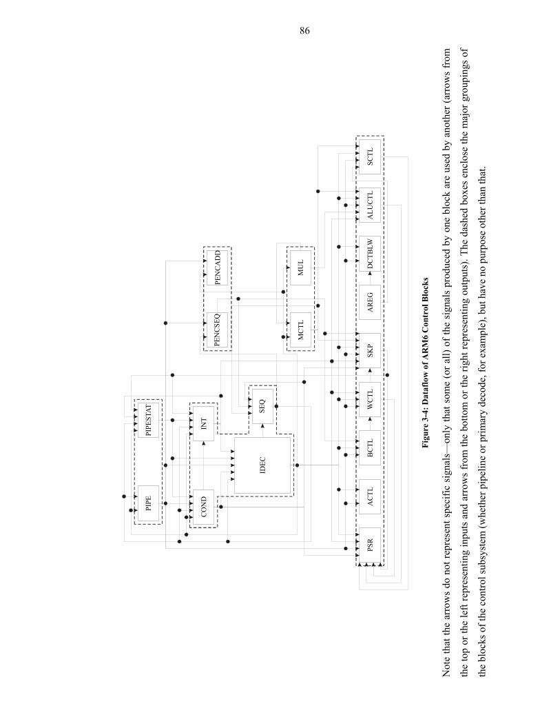
86
IDEC
PIPE
PIPE
STAT
INT
CO
ND
SEQ
MC
TLM
UL
PEN
CSE
QPE
NC
AD
D
AC
TLB
CTL
WC
TLPS
RSK
PA
REG
DC
TBLW
SCTL
ALU
CTL
Figu
re 3
-4: D
ataf
low
of A
RM
6 C
ontr
ol B
lock
s
Not
e th
at th
e ar
row
s do
not
repr
esen
t spe
cific
sig
nals
—on
ly th
at s
ome
(or a
ll) o
f the
sig
nals
pro
duce
d by
one
blo
ck a
re u
sed
by a
noth
er (a
rrow
s fr
om
the
top
or th
e le
ft re
pres
entin
g in
puts
and
arr
ows
from
the
botto
m o
r the
righ
t rep
rese
ntin
g ou
tput
s). T
he d
ashe
d bo
xes
encl
ose
the
maj
or g
roup
ings
of
the
bloc
ks o
f the
con
trol s
ubsy
stem
(whe
ther
pip
elin
e or
prim
ary
deco
de, f
or e
xam
ple)
, but
hav
e no
pur
pose
oth
er th
an th
at.
87
when the instruction being executed directly writes to the program counter,
whereas the abort status is set if the instruction fetch itself caused the abort.
• Primary Decode:
♦ COND: in the first clock cycle of the execution of an instruction this block
determines whether the instruction passes its condition code.
♦ IDEC: generates the signals that the Secondary Decode blocks (see below) use
to generate the signals that control the datapath. These signals are generated for
the instruction step indicated by the SEQ block using the opcode of the instruction
being executed or that of the next instruction to be executed, as appropriate.
♦ INT: detects interrupts and exceptions. This block indicates when to handle
interrupts and exceptions (recording status information as required), prioritising if
more than one is pending.
♦ SEQ: determines the instruction step that should be decoded this clock cycle
(that is, the next step of the instruction currently being executed or the first step of
the next instruction to be executed).
• [Instruction Non-specific] Secondary Decode
♦ ACTL: selects the address field used for data register bank read port which
outputs onto the RA bus (but not which register set to access).
♦ ALU: buffers an IDEC control signal to help determine when the ALUA latch
should be transparent.
♦ ALUCTL: generates the signals that control the ALU datapath component
(function select and carry select).
♦ AREG: buffers the bottom two bits of the address register so byte extraction and
misaligned word rotation may be performed properly on the values resulting from
memory read accesses.
♦ BCTL: selects the address field used for the data register bank read port which
outputs onto the RB bus (but not which register set to access).
♦ DCTLBW: generates the signal that controls the replicator datapath component
and the signal that controls the field extractor datapath component.
♦ PSR: generates the signal that controls the register set the data register bank ports
should operate on, buffers the appropriate program status registers as required and
generates the signal that controls the operation of the PSRDAT multiplexer.
88
♦ SCTL: selects the signal that controls the barrel shifter datapath component,
buffers the value used for register controlled shifts and adjusts the shifter carry out
for some register controlled shifts.
♦ SKP: generates the signal that controls the AREG multiplexer, the signals that
control bus cycles and those that control whether the data register bank write ports
are active.
♦ WCTL: selects the address field used for the data register bank write port which
receives input from the ALU bus (but not which register set to access).
• [Multiplication Specific] Secondary Decode
♦ MCTL: generates the signal that controls the shift amount of the barrel shifter
datapath component, the signal that indicates whether to borrow to ALUCTL and
the signal that indicates whether the multiplication has terminated.
♦ MUL: buffers the value of the multiplier to provide the sequence of bit slices that
the MCTL and the ALUCTL blocks require to generate the sequence of signals
that control the operation of the barrel shifter and the ALU datapath components
to implement a 2-bit Booth’s algorithm. It also generates the signal that indicates
whether all the bits in the multiplier have been used yet.
• [Block Transfer Specific] Secondary Decode
♦ PENCADD: counts the number of 1’s in the bottom sixteen bits of an instruction
and selects the offset, if any, required for address calculation. (Branches and
exception entry also make use of this block to select the offset to adjust the value
of the program counter by, for the appropriate return address.)
♦ PENCSEQ: generates the address field of the highest priority unused register,
specified in the transfer list, for the BCTL and WCTL blocks, as well as the signal
that indicates whether all registers in the transfer list have been used yet.
3.3 Summary
The behaviour of most instructions defined by the Programmer’s Model of the ARM6
(except only that of control modifiers and instruction set extenders—see section 3.1.4),
is dependent on a significant number of options (see section 3.1.5). This is reflected in
added complexity in the control logic of the Hardware Implementation of the ARM6
(see section 3.2.4). Nonetheless, this also makes the ARM6 of interest for specification
(see section 4 and section 6).
89
4 Specifying the ARM6 The methodology of this thesis was primarily developed in the process of specifying
the original ARM6. Therefore this section focuses on what this specification involved—
section 4.1—and how it was developed with respect to each of the three presentations
used with this specification—section 4.2, section 4.3 and section 4.4 (see section 2.3
for details on the method underlying each presentation).
4.1 General Principles
The following instruction classes were used to specify the ARM6:
•CONTROL INSTRUCTIONS
♦ br: encapsulates flow modifiers (see section 3.1.4).
♦ swi_ex: encapsulates mode modifiers (see section 3.1.4) and exceptions raised by
external events (see section 3.1.2) such as interrupts and memory aborts.
• DATA PROCESSING OPERATIONS
♦ data_proc: encapsulates arithmetic operations, data register transfer operations
and logical operations (see section 3.1.4) with immediates or immediate shifts
(see section 3.1.5).
♦ mla_mul: encapsulates multiplication operations (see section 3.1.4).
♦ mrs_msr: encapsulates transfer operations involving the program status registers
(see section 3.1.4).
♦ reg_shift: encapsulates arithmetic operations, data register transfer operations and
logical operations (see section 3.1.4) with register shifts (see section 3.1.5).
• MEMORY INSTRUCTIONS
♦ ldm: encapsulates block data transfers from memory to the ARM6 processor core
(see section 3.1.4).
♦ ldr: encapsulates single data transfers from memory to the ARM6 processor core
(see section 3.1.4).
♦ stm: encapsulates block data transfers from the ARM6 processor core to memory
(see section 3.1.4).
♦ str: encapsulates single data transfers from the ARM6 processor core to memory
(see section 3.1.4).
♦ swp: encapsulates semaphore instructions (see section 3.1.4).
90
• COPROCESSOR INSTRUCTIONS
♦ cdp_und: encapsulates coprocessor data operations (see section 3.1.4).
♦ ldc_stc: encapsulates coprocessor data transfers (see section 3.1.4).
♦ mcr: encapsulates transfer of register value from processor core to coprocessor
(see section 3.1.4).
♦ mrc: encapsulates transfer of value from coprocessor to processor core register
(see section 3.1.4).
• INSTRUCTION SET EXTENDERS
♦ cdp_und: encapsulates undefined instructions (see section 3.1.4).
• NULL INSTRUCTIONS
♦ unexec: substituted for the instruction class that would otherwise have entered
the Execute stage when the pipeline control logic detects that the instruction class
failed its condition code (see section 3.1.4).
Note that arithmetic operations, data register transfer operations and logical operations
are all included in one instruction class because these differ primarily in what operation
is performed, not how it is performed. Indeed, sufficient similarity also exists between
arithmetic operations, data register transfer operations and logical operations that use
immediate shifts and those that use an immediate, for these to be in one instruction class
as well. Still, this is not so for arithmetic operations, data register transfer operations
and logical operations that involve register shifts and those that involve an immediate,
or an immediate shift, since the former require an instruction step to initialise the shift.
Though the final instruction step is in common, to define one instruction class, not two,
would introduce unnecessary complications (see section 2.2.3).
It may seem odd to use one, instead of two separate, instruction classes to encapsulate
coprocessor data operations and undefined instructions. However, as far as the ARM6
processor core is concerned a coprocessor data operation is an undefined instruction that
one coprocessor may accept and an undefined instruction is a coprocessor instruction
every coprocessor must reject.
The instruction classes used to specify the ARM6 were decomposed into the following
instruction steps (see Table 2-5 for the key to the timing annotation used to denote
individual instruction steps):
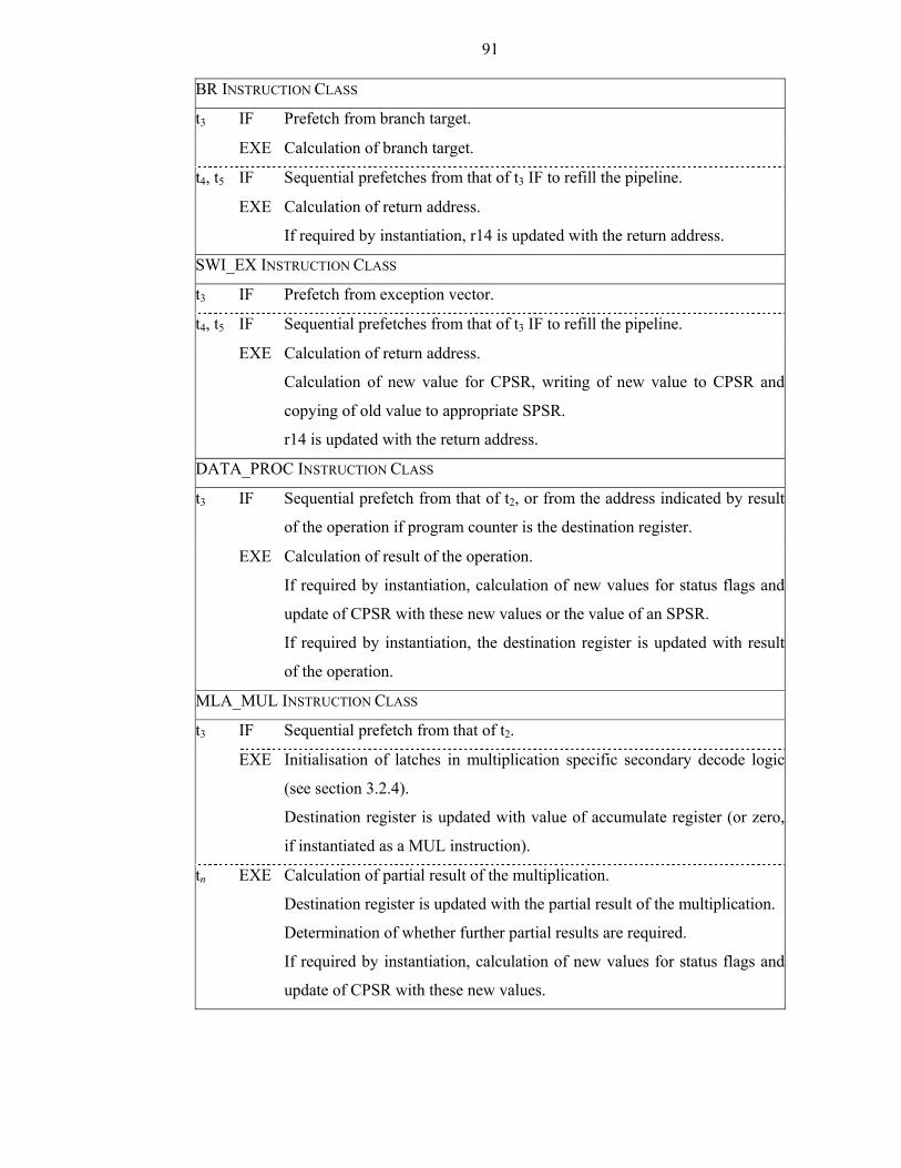
91
BR INSTRUCTION CLASS
t3 IF Prefetch from branch target.
EXE Calculation of branch target.
t4, t5 IF Sequential prefetches from that of t3 IF to refill the pipeline.
EXE Calculation of return address.
If required by instantiation, r14 is updated with the return address.
SWI_EX INSTRUCTION CLASS
t3 IF Prefetch from exception vector.
t4, t5 IF Sequential prefetches from that of t3 IF to refill the pipeline.
EXE Calculation of return address.
Calculation of new value for CPSR, writing of new value to CPSR and
copying of old value to appropriate SPSR.
r14 is updated with the return address.
DATA_PROC INSTRUCTION CLASS
t3 IF Sequential prefetch from that of t2, or from the address indicated by result
of the operation if program counter is the destination register.
EXE Calculation of result of the operation.
If required by instantiation, calculation of new values for status flags and
update of CPSR with these new values or the value of an SPSR.
If required by instantiation, the destination register is updated with result
of the operation.
MLA_MUL INSTRUCTION CLASS
t3 IF Sequential prefetch from that of t2.
EXE Initialisation of latches in multiplication specific secondary decode logic
(see section 3.2.4).
Destination register is updated with value of accumulate register (or zero,
if instantiated as a MUL instruction).
tn EXE Calculation of partial result of the multiplication.
Destination register is updated with the partial result of the multiplication.
Determination of whether further partial results are required.
If required by instantiation, calculation of new values for status flags and
update of CPSR with these new values.
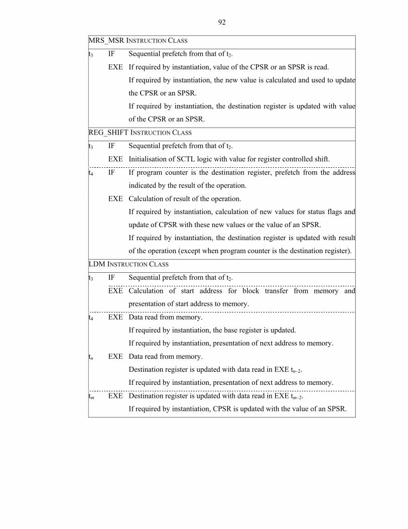
92
MRS_MSR INSTRUCTION CLASS
t3 IF Sequential prefetch from that of t2.
EXE If required by instantiation, value of the CPSR or an SPSR is read.
If required by instantiation, the new value is calculated and used to update
the CPSR or an SPSR.
If required by instantiation, the destination register is updated with value
of the CPSR or an SPSR.
REG_SHIFT INSTRUCTION CLASS
t3 IF Sequential prefetch from that of t2.
EXE Initialisation of SCTL logic with value for register controlled shift.
t4 IF If program counter is the destination register, prefetch from the address
indicated by the result of the operation.
EXE Calculation of result of the operation.
If required by instantiation, calculation of new values for status flags and
update of CPSR with these new values or the value of an SPSR.
If required by instantiation, the destination register is updated with result
of the operation (except when program counter is the destination register).
LDM INSTRUCTION CLASS
t3 IF Sequential prefetch from that of t2.
EXE Calculation of start address for block transfer from memory and
presentation of start address to memory.
t4 EXE Data read from memory.
If required by instantiation, the base register is updated.
If required by instantiation, presentation of next address to memory.
tn EXE Data read from memory.
Destination register is updated with data read in EXE tn–2.
If required by instantiation, presentation of next address to memory.
tm EXE Destination register is updated with data read in EXE tm–2.
If required by instantiation, CPSR is updated with the value of an SPSR.
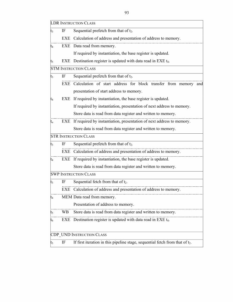
93
LDR INSTRUCTION CLASS
t3 IF Sequential prefetch from that of t2.
EXE Calculation of address and presentation of address to memory.
t4 EXE Data read from memory.
If required by instantiation, the base register is updated.
t5 EXE Destination register is updated with data read in EXE t4.
STM INSTRUCTION CLASS
t3 IF Sequential prefetch from that of t2.
EXE Calculation of start address for block transfer from memory and
presentation of start address to memory.
t4 EXE If required by instantiation, the base register is updated.
If required by instantiation, presentation of next address to memory.
Store data is read from data register and written to memory.
tn EXE If required by instantiation, presentation of next address to memory.
Store data is read from data register and written to memory.
STR INSTRUCTION CLASS
t3 IF Sequential prefetch from that of t2.
EXE Calculation of address and presentation of address to memory.
t4 EXE If required by instantiation, the base register is updated.
Store data is read from data register and written to memory.
SWP INSTRUCTION CLASS
t3 IF Sequential fetch from that of t2.
EXE Calculation of address and presentation of address to memory.
t4 MEM Data read from memory.
Presentation of address to memory.
t5 WB Store data is read from data register and written to memory.
t6 EXE Destination register is updated with data read in EXE t4.
CDP_UND INSTRUCTION CLASS
t3 IF If first iteration in this pipeline stage, sequential fetch from that of t2.
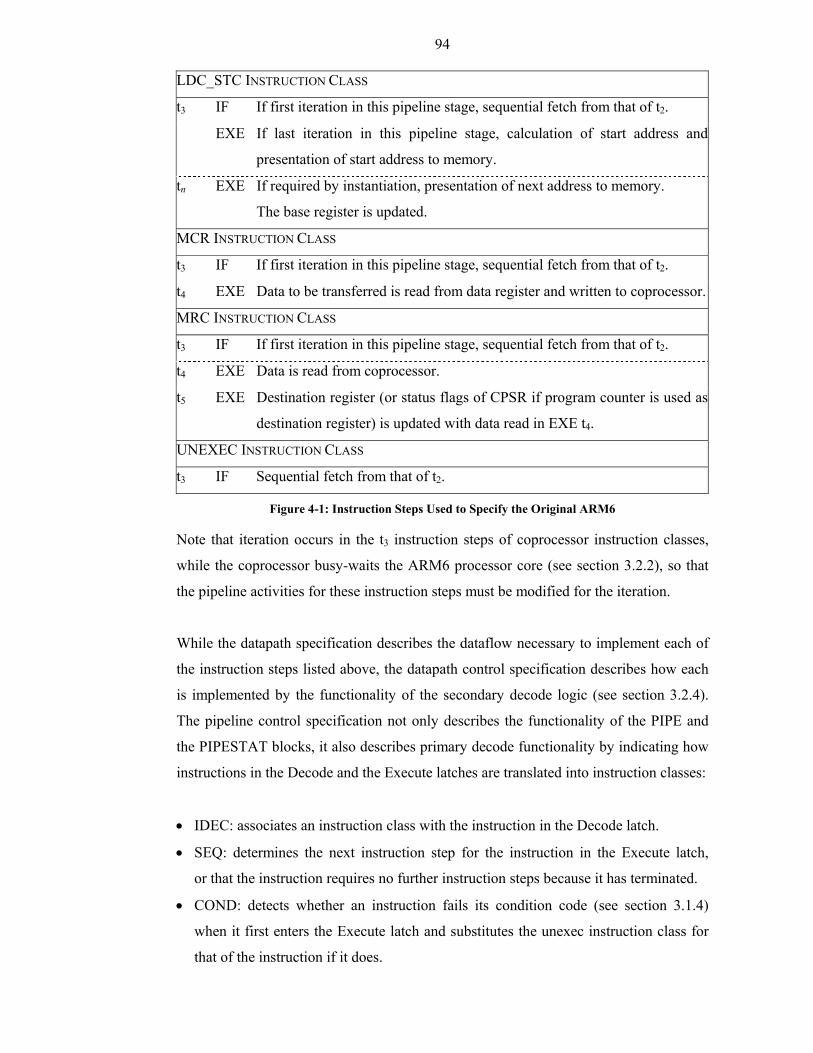
94
LDC_STC INSTRUCTION CLASS
t3 IF If first iteration in this pipeline stage, sequential fetch from that of t2.
EXE If last iteration in this pipeline stage, calculation of start address and
presentation of start address to memory.
tn EXE If required by instantiation, presentation of next address to memory.
The base register is updated.
MCR INSTRUCTION CLASS
t3 IF If first iteration in this pipeline stage, sequential fetch from that of t2.
t4 EXE Data to be transferred is read from data register and written to coprocessor.
MRC INSTRUCTION CLASS
t3 IF If first iteration in this pipeline stage, sequential fetch from that of t2.
t4 EXE Data is read from coprocessor.
t5 EXE Destination register (or status flags of CPSR if program counter is used as
destination register) is updated with data read in EXE t4.
UNEXEC INSTRUCTION CLASS
t3 IF Sequential fetch from that of t2.
Figure 4-1: Instruction Steps Used to Specify the Original ARM6
Note that iteration occurs in the t3 instruction steps of coprocessor instruction classes,
while the coprocessor busy-waits the ARM6 processor core (see section 3.2.2), so that
the pipeline activities for these instruction steps must be modified for the iteration.
While the datapath specification describes the dataflow necessary to implement each of
the instruction steps listed above, the datapath control specification describes how each
is implemented by the functionality of the secondary decode logic (see section 3.2.4).
The pipeline control specification not only describes the functionality of the PIPE and
the PIPESTAT blocks, it also describes primary decode functionality by indicating how
instructions in the Decode and the Execute latches are translated into instruction classes:
• IDEC: associates an instruction class with the instruction in the Decode latch.
• SEQ: determines the next instruction step for the instruction in the Execute latch,
or that the instruction requires no further instruction steps because it has terminated.
• COND: detects whether an instruction fails its condition code (see section 3.1.4)
when it first enters the Execute latch and substitutes the unexec instruction class for
that of the instruction if it does.
95
• INT: detects when exceptions occur (see section 3.1.2) and it causes the swi_ex
instruction class to be substituted for that of the instruction in the Decode latch,
when it is appropriate for the exception to be taken.
4.2 Mathematical Presentation
More than one attempt was required to generate the Phase specification of the ARM6:
two were made before the successful attempt that resulted in a complete specification.
(The methodology presented in section 2.3.1 derives from this third attempt). Both of
the unsuccessful attempts partitioned the specification into a datapath specification and
a datapath control specification, but did not separate the pipeline control specification
from the datapath control specification. In contrast to the second and the third attempts,
the first attempt did not attempt to distinguish specification of the pipeline activities
associated with each pipeline stage from the specification of each pipeline stage itself.
Indeed while the first attempt used a structural approach for the datapath specification,
the approach used for the datapath control specification was intended to be executable.
The structural approach decomposed the specification of each instruction class into
specifying the behaviour exhibited as an instruction of that instruction class occupies
the Instruction Fetch stage, the Instruction Decode stage and then the Execute stage.
The other approach decomposed the specification of each instruction class into
specifying the behaviour that an instruction of that instruction class causes as it occupies
the Instruction Decode stage and the Execute stage (but the behaviour was labelled
according to the pipeline stage, not the pipeline activity).
Work to specify the ARM6 using the methodology of the first attempt was discontinued
when it became clear that using two distinct approaches for the datapath specification
and the datapath control specification did not so much provide for different perspectives
as it did confusion. Moreover, without subdivision into constituent pipeline activities,
the specification of some of the instruction steps in the datapath control specification
lacked definition in terms of overall function. The second attempt to specify the ARM6
solved most of these problems by using a layout much the same as that of Figure 2-6 for
its datapath specification and that of Figure 2-7 for its datapath control specification.
The primary difference in layouts between the second attempt and the third attempt
involves how the behaviour associated with the Instruction Fetch stage, as an instruction
progresses through the instruction pipeline, is specified. The datapath specification of
96
the second attempt describes how the instruction of the instruction class being specified
is read from memory at t1, whereas that of the third attempt only specifies an instruction
is read from memory at t3. Additionally the datapath specification of the second attempt
describes how the program counter is incremented in the Instruction Fetch stage at t1,
and at t2, so that the program counter reads as the address of the instruction plus eight in
the Execute stage. The datapath specification of the third attempt leaves this implicit in
the behaviour associated with the Instruction Fetch pipeline activities of the instructions
that preceded the instruction of the instruction class being specified. These differences
arguably result from the main difference between the methodology of the second and
the third attempts to specify the ARM6: whether the pipeline control specification and
the datapath control specification are two distinct specifications.
Since the second attempt to specify the ARM6 did not separate datapath control and
pipeline control, functions that would be defined once in a pipeline control specification
had to be duplicated across every instruction class of the datapath control specification.
This not only obscured the independence of these functions from the instruction class
being specified, but also unnecessarily complicated the process of understanding how
the specifications of the instruction classes of the instructions in the instruction pipeline
should be combined to indicate the behaviour expected of the ARM6 processor core.
Consequently, work to specify the ARM6 using the methodology of the second attempt
was discontinued, when these disadvantages became apparent, and work was begun
using the methodology from which that outlined in section 2.3.1 is derived.
The use of notation for pipeline latches to avoid the necessity to explicitly name signals
buffered from previous pipeline stages was first developed for the modernised ARM6
(see section 6.2) and is discussed as part of the general methodology in section 2.3.1.
Still, the Phase specification of the original ARM6 would not significantly benefit from
the use of this notation, as little of the datapath of the original ARM6 is pipelined and
the abstraction of instruction steps encapsulates most, if not all, of the control signals
buffered from the Instruction Decode stage to the Execute stage in the original ARM6.
However, using notation for a pipeline latch between the Instruction Decode stage and
the Execute stage for the few signals, such as NXTIC[*], that require buffering between
two pipeline stages, would make the style of the specification of the original ARM6
more consistent with that of the modernised ARM6.
97
Nonetheless, many of the features of the general methodology discussed in section 2.3.1
were developed in the process of creating the Phase specification of the original ARM6,
before work on the Phase specification of the modernised ARM6 began. For example:
• The primary technique of abstraction used in the datapath specification pertains to
the use of outputs from combinational logic, such as a multiplexer or a barrel shifter,
in transfers without specifying the operation that the combinational logic performs.
This allows the definition of instruction classes to abstract over instructions of
similar function that perform the same transfers. However, problems arise when
dealing with instructions of similar function that do not perform the same transfers.
For instance, the base register of single data transfer instructions is updated only if
the P and the W bits in the encoding of the instruction have the appropriate values,
while data processing instructions and multiplication instructions update the CPSR
only if the S bit is set (see section 3.1.5). Defining separate instruction classes for
when the transfer occurs, and when it does not, would unduly increase the number of
instruction classes that need to be defined given that several instruction classes
would be identical but for one transfer. Hence, the notation of curly braces enclosing
an entire transfer was developed to indicate when the transfer may or may not occur
depending on the value of the write enable signal the datapath control specification
associates with the write port. (Note the datapath specification of an instruction class
may include transfers that are still performed but are unnecessary in one or more of
its instantiations, which is different because this reflects redundancy in the design.
For example, an instantiation of the multiplication instruction class that does not add
an initial value to the multiplication result, still performs the register read to produce
this initial value and the transfers so one of the inputs of the ALU is driven with it,
even though the ALU will output zero regardless of its inputs in this case.)
• The Programmer’s Model of the ARM6 assigns every instruction a condition code
(see section 3.1.4), such that the Phase specification of the ARM6 must describe how
an instruction that fails its condition code does not execute. Initially the solution used
reflected that used in the design: a function was defined to specify the signal that
indicates if an instruction failed its condition code while functions defined to specify
signals that indicate whether effects, visible at the Programmer’s Model specification
level of abstraction, should occur, checked this signal. Nevertheless, this introduces
asymmetry between the datapath and the datapath control specifications in terms of
how evident it is that behaviour occurs only if the instantiation of an instruction class
98
does not fail its condition code. Moreover, the definition of a significant number of
the functions defined by the datapath control specification of every instruction class
was complicated by the need to check whether the condition code had been failed.
Therefore this approach was abandoned with the third attempt to specify the ARM6
in favour of creating an instruction class (that is, unexec) to specify the behaviour of
an instruction that fails its condition code, which can be substituted, as specified by
the pipeline control specification, for another instruction class. Since it is determined
whether an instruction has passed its condition code in the Execute stage rather than
the Instruction Decode stage, the substitution occurs with respect to the IC function
and not the NXTIC function (as mentioned in section 2.3.1). Note that this approach
would not be possible using the methodologies of the first two attempts to specify
the ARM6, since it is not possible to specify the substitution of one instruction class
for another as part of the Phase specification itself without separate pipeline control
and datapath control specifications.
• The development of a strategy for timing annotations as shown in Table 2-5 and
discussed in section 2.3.1 was motivated by the need to specify instruction classes,
such as swp, which iterate in the Execute stage without iterating pipeline activities,
or ldm, which may also iterate in the Execute stage with identical pipeline activities
(see Figure 4-1). This strategy was created for the first attempt to specify the ARM6
and used without significant changes in subsequent attempts. Before the third attempt
to specify the ARM6, the Phase specification did not itself describe how
specifications of the instruction classes of the instructions in the instruction pipeline
should be combined to indicate the behaviour expected of the ARM6 processor core.
This is not so much of an omission when iteration cannot occur in any pipeline stage,
because each instruction class consists of the same sequence of instruction steps.
Thus to combine the specifications, it is a simple matter to select the instruction step
associated with each pipeline stage by the instruction that the pipeline stage contains
and aggregate the pipeline activities, if any, associated with each instruction step.
However, the situation is more complex when iteration can occur (as shown by
Table 2-1 and Table 2-2), so to be able to specify this in the Phase specification itself
was one of the main reasons behind separating the pipeline control specification and
the datapath control specification. The separate pipeline control specification allows
the NXTIC, the IC, the NXTIS and the IS functions to be defined. These functions
indicate which instruction steps specify the pipeline activities that need combining;
as discussed in section 2.3.1 as part of the general methodology of this thesis.
99
As noted in section 6.2, types were defined to package together the signals used to drive
register read ports and register write ports in the specification of the original ARM6
since this allowed each read port and each write port to be characterised by one signal
(albeit an abstract signal). However, as explained in the detailed discussion of this issue
in section 6.2, this abstraction was not appropriate for the modernised ARM6;
consequently it was not included in the general methodology presented in section 2.3.1.
The ARM6 uses two different methods to resolve the control hazards that result from
modifying the value of the program counter in the Execute stage—instead of updating it
with the value from the incrementer—because the prefetch queue holds two instructions
fetched with the assumption that the program counter would be updated with the value
from the incrementer. One method relies on the observation that control instructions
iterate three times in the Execute stage, and that if the modification is made in the first,
the instructions in the prefetch queue will be replaced with the instructions that succeed
the instruction fetched for the new value of the program counter. The other method
marks the instructions in the prefetch queue invalid and requires that the unexec
instruction class be substituted for that of any instructions thus marked such that
subsequent instruction fetches can introduce valid instructions into the prefetch queue.
Specification of the instruction classes that use the first method for the resolution of
control hazards is sufficient to specify the first method, since it is an integral feature of
each instruction class that uses it. However, specification of the second method requires
interaction between the datapath control and the pipeline control specifications,
because the latter specification must detect when the former specification indicates that
the program counter has been modified and invalidate instructions in the prefetch queue
as necessary. If one control specification was used instead of two, the second method
could not be specified as just described, to reflect its implementation in the design;
instead it would have to be specified similarly to the first method and thus complicate
the specification of instruction classes that can modify the program counter.
4.3 Engineering Presentation
The methodology documented in section 2.3.2 reflects that developed in the process of
creating the engineering presentation of the formal specification of the original ARM6
from the mathematical presentation. No problems were encountered in this process,
since any that would have been discovered had already been solved in order to create
the mathematical presentation.
100
4.4 Executable Presentation
Several versions of the executable presentation of the Phase specification of the ARM6
were developed before the one from which the methodology described in section 2.3.3
is derived. In contrast to the first two attempts to develop the mathematical presentation,
every superseded version of the executable presentation, but the first, was complete and
deprecated only to add new features or optimise existing features. The versions
primarily differ with respect to the implementation of the reusable modules rather than
that of the modules particular to each executable presentation. Indeed, the modules
particular to each executable presentation only differ between versions when changes in
the interface of the reusable modules must be reflected in how these modules are used.
The versions of the executable presentation developed for the Phase specification of
the ARM6 may be summarised as follows.
1. This version was primarily derived from the mathematical presentation, in contrast to
the following versions which are mainly derived from the engineering presentation.
Instead of the modules particular to each executable presentation discussed in
section 2.3.3, and used by the following versions, this version uses one
specification.sml module, which defines a datapath function and a pipeline function.
These functions do not perform transfers or calculations but return a pair to indicate
the transfers and the calculations that should be performed by the reusable modules.
Although this had the advantage of representing the Phase specification of the ARM6
more as a data structure than as part of the simulator itself and thus would facilitate
using this representation with other programs, the verboseness of this approach
rendered the representation difficult to follow. Moreover, this approach depended on
the feature of the ML programming language that allows functions to be passed as
arguments to, or results of, other functions. This feature is not as well supported by
non-functional programming languages and thus this approach unnecessarily restricts
the languages that could be used to implement the executable presentation.
2. The second version was the first complete version of an executable presentation of
the Phase specification of the ARM6. It implemented the reusable modules as well as
the modules particular to each executable presentation largely as discussed in
section 2.3.3 with the following major exceptions. The digital_value abstract type
was comprised by a function to indicate which bits of the word were in fact valid and
a 32-tuple to correspond to the 32-bit word. (Although this use of functions relies on
101
the same feature of functional programming languages as deprecated for version 1,
this usage is part of the interface of the digital_value abstract type and thus could be
redesigned for other programming languages that do not support this feature without
much modification to the executable presentation of the Phase specification itself.)
No trace abstract type was implemented in the buses.sml module and the memory
abstract type was defined as an association list of instances of the digital_value
abstract type (with one element of the pair for the address and the other for the data
stored at the address). The state.sml module was much simpler with no support for
memory aborts, other than as scheduled by environment events (see section 2.3.3),
no tube abstract type, and the environment abstract type maintaining association lists
for the input and the output abstract types directly rather than using the core_inputs
and the core_outputs abstract types. Finally, error conditions were allowed to raise
Bind, Match, and Option.Option exceptions directly according to the assumption that
was incorrect due to the error condition, such that handle expressions were required
to display appropriate error messages.
3. A number of variants of the third version were implemented in order to evaluate
potential optimisations and new features. Nonetheless, all variants were derived from
version 2 and used guard and guardf syntactic sugar to manage error conditions by
just raising one type of exception with an appropriate error message (see Appendix C
for examples), thus reducing the amount of work required to handle error conditions.
In addition, the tube abstract type was introduced to improve support for simulating
the test vectors that ARM Ltd. developed for validating the original ARM6.
a. Several variants of the digital_value abstract type were created to evaluate
optimisations to how iteration over the elements of the 32-tuple is performed and
to make more use of tail recursion in recursive function definitions.
b. Several variants of the memory abstract type were created to evaluate using arrays
to represent memory (as discussed in section 2.3.3), rather than an association list,
and using functions that are maintained by the memory abstract type to indicate
which memory addresses the memory subsystem should abort. The use of arrays
produced significantly faster simulations and the use of functions for aborts
proved more convenient than environment events, so both these modifications
were incorporated into later versions of the executable presentation as standard.
c. Two variants were created to assess how trace information might be produced by
the simulator. The first variant maintained trace information for each clock phase
as an item in a list ordered according to the number of clock phases since
102
simulation began. (Each item is an optional array of an optional array of the traces
union type with each element in the array of arrays maintaining data for the signal
dictated by the correspondence of the indices of the element to the group in which
state_insert_buses is invoked on the signal and the position of the signal within
this group. This method of mapping a signal onto the indices of an array of arrays
is the same as that used by the trace abstract type discussed in section 2.3.3.)
Although this allowed the trace information to be recorded reasonably efficiently
during simulation, the trace information needed to be resorted in order of signals
to write the trace file and the time required to do this increased significantly with
the number of clock phases traced. Therefore the second variant was developed,
which indexes trace information by signal during simulation and not just when
writing the trace file. The second variant slows simulation more than the first
since it requires more work to be done on each new clock phase than just adding
a new item to a list. Still this decrease was much less significant than the increase
in the speed with which the trace file is written. Hence the trace abstract type
implemented by the second variant was the one incorporated into later versions of
the executable presentation as standard.
4. This version modified the interface to the digital_value abstract type to not expose
the way in which the implementation of this type determines which bits of the word
encapsulated by an instance of this type are valid, but require a list of bit ranges that
the implementation itself converts to the internal implementation. This facilitated
evaluation of different definitions for the digital_value abstract type, as modules that
use the digital_value abstract type did not require any further modifications.
Different combinations of n-tuples, functions, arrays and vectors were considered
and the 32-element array and 32-element vector pair referred to in the definition of
the digital_value abstract type was the most efficient. Hence this was the one
incorporated into later versions of the executable presentation as standard, along with
various optimisations to the digital_value abstract type that became possible due to
the use of this definition (see the common.sml subsection of Appendix C).
5. This was the last version created and modified how the environment abstract type
maintains its collections of input and output abstract types to use the core_inputs and
the core_outputs abstract types (see the signals.sml subsection of Appendix C)
instead of association lists of instances of the input and the output abstract types.
This change was included in the general methodology discussed in section 2.3.3 as it
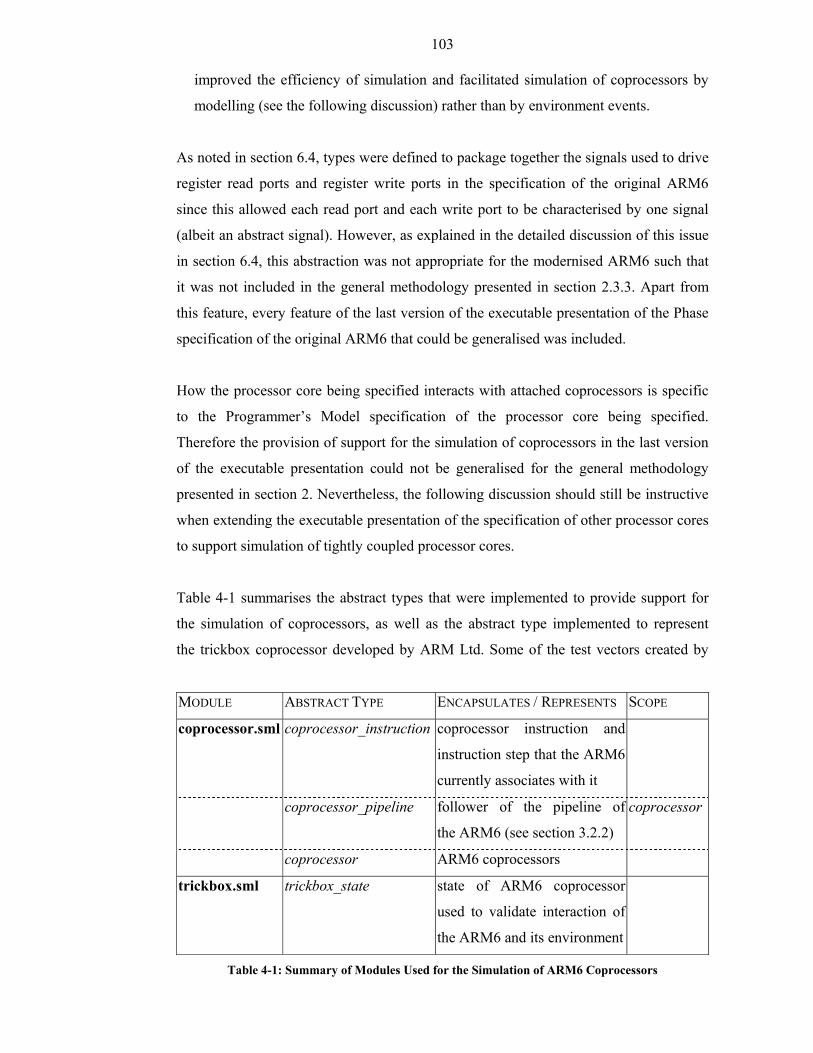
103
improved the efficiency of simulation and facilitated simulation of coprocessors by
modelling (see the following discussion) rather than by environment events.
As noted in section 6.4, types were defined to package together the signals used to drive
register read ports and register write ports in the specification of the original ARM6
since this allowed each read port and each write port to be characterised by one signal
(albeit an abstract signal). However, as explained in the detailed discussion of this issue
in section 6.4, this abstraction was not appropriate for the modernised ARM6 such that
it was not included in the general methodology presented in section 2.3.3. Apart from
this feature, every feature of the last version of the executable presentation of the Phase
specification of the original ARM6 that could be generalised was included.
How the processor core being specified interacts with attached coprocessors is specific
to the Programmer’s Model specification of the processor core being specified.
Therefore the provision of support for the simulation of coprocessors in the last version
of the executable presentation could not be generalised for the general methodology
presented in section 2. Nevertheless, the following discussion should still be instructive
when extending the executable presentation of the specification of other processor cores
to support simulation of tightly coupled processor cores.
Table 4-1 summarises the abstract types that were implemented to provide support for
the simulation of coprocessors, as well as the abstract type implemented to represent
the trickbox coprocessor developed by ARM Ltd. Some of the test vectors created by
MODULE ABSTRACT TYPE ENCAPSULATES / REPRESENTS SCOPE
coprocessor.sml coprocessor_instruction coprocessor instruction and
instruction step that the ARM6
currently associates with it
coprocessor_pipeline follower of the pipeline of
the ARM6 (see section 3.2.2)
coprocessor
coprocessor ARM6 coprocessors
trickbox.sml trickbox_state state of ARM6 coprocessor
used to validate interaction of
the ARM6 and its environment
Table 4-1: Summary of Modules Used for the Simulation of ARM6 Coprocessors
104
ARM Ltd. to validate the original ARM6 use the trickbox coprocessor, thus including
support for the trickbox coprocessor in the executable presentation of the specification
of the original ARM6 facilitated simulation of these test vectors for this thesis.
The following minor changes to the state.sml module (see section 2.3.3) were necessary
to provide support for the simulation of coprocessors:
• The tuple used to define the environment abstract type was altered to include a list of
coprocessor abstract type instances and an environment_add_coprocessor function
was defined to manage adding instances of the coprocessor abstract type to this list
(and thus to simulate attaching a coprocessor to the ARM6 processor core).
• The environment_init_inputs function was altered to invoke coprocessor_update on
every instance of the coprocessor abstract type in the list maintained by the specified
instance of the environment abstract type. (The coprocessor_update function is used
to coordinate the simulation of the behaviour of the relevant coprocessor. It arranges
the updating of the instance of the coprocessor_pipeline abstract type maintained by
the specified instance of the coprocessor abstract type, according to the specified
instance of the core_inputs abstract type, to simulate the pipeline follower behaviour.
In addition, it organises creation of appropriate instances of the inputs abstract type
to represent the signals that the relevant coprocessor should drive when the function
is invoked.)
To avoid the necessity of further changes to the state.sml module, the coprocessor
abstract type should be used to encapsulate ARM6 coprocessors as follows:
1. By maintaining the number associated with the coprocessor, it can determine which
coprocessor instructions apply to the coprocessor (by checking the cp_number field
of the coprocessor instruction opcode—see section 3.1.5).
2. By maintaining the instruction step, in terms of the ARM6 processor core pipeline,
that the coprocessor should create instances of the inputs abstract type in response to,
in order to simulate driving signals to the ARM6 processor core. Note that because
the processor core, not the coprocessor, is being specified, it is sufficient to model
the behaviour of the coprocessor rather than how this behaviour is implemented.
Hence it may not be necessary to model further the details of how the coprocessor
pipelines instructions.
105
3. By maintaining the function that models the behaviour of the coprocessor in terms of
the signals that should be driven in response to the instruction step currently being
processed by the ARM6 processor core, this function may be invoked as appropriate
by the coprocessor_update function.
Therefore any ARM6 coprocessor may be represented by instantiating the coprocessor
abstract type with an appropriate function to specify its behaviour and a number that
should be associated with it. Nonetheless, if it is necessary to maintain state between
different invocations of the function that models the behaviour of the coprocessor,
reference primitive types must be used such that although the bindings referenced by
the function cannot change, what the bindings reference can. This use of reference
primitive types does not complicate mathematical representation of the executable
presentation of the Phase specification of the ARM6, as the interface of the coprocessor
abstract type does not expose these types. Indeed, it not only improves simulation
efficiency, but it also facilitates generalisation of the coprocessor abstract type because
any state that an instantiation may require is not exposed by the function used to create
the instantiation.
The execution of every applicable test of the ARM6 validation test suite developed by
ARM Ltd. on the design described by the Phase specification of the original ARM6
was simulated using the executable presentation so that all of the following were tested:
1. Reset behaviour.
2. Every instruction defined by the Programmer’s Model specification.
3. Data abort behaviour.
4. Prefetch abort behaviour.
5. FIQ and IRQ behaviour.
6. Every coprocessor interaction.
This involved the simulation of approximately 2.5 million instructions and 4.75 million
clock cycles. The mean CPI (clock cycles per instruction) of the design was around 1.9
for the simulated tests. (However, as validation tests are often atypical of programs that
will be run on processors this CPI can be no more than a guide.) Mean simulation speed
was approximately 880 clock cycles per second or around 460 instructions per second.
(Simulation was performed using the PolyML 4.1.2 implementation of Standard ML,
106
which may be downloaded at http://www.polyml.org/, on a 1GHz Intel Pentium III PC
under the Linux operating system.)
4.5 Summary
Significant work was involved in developing the methodology of this thesis to create
the Phase specification of the original ARM6. However, this had the advantage that
relatively few changes were required before this methodology could be used to create
Phase specifications of the modernised ARM6 (see section 6.5), the MIPS R2000 and
the DLX (see section 7.6).
The creation of the Phase specification of the original ARM6 serves to demonstrate that
the methodology of this thesis is applicable even to commercial processor core designs,
which are often quite complex. In particular, the methodology of this thesis provided
elegant solutions to describing relatively large numbers of instruction classes,
coprocessor interactions, pipelined addressing and the complexities that result from
irregular instruction set encodings.
107
5 Overview of the Modernised ARM6 The original ARM6 was designed in the early 1990s, and as such, its design no longer
represents the state of the art in processor design. Consequently, some of the methods
used to design modern processors were considered as part of the work for this thesis,
and of these, several were used to develop a modernised ARM6 that better represents
modern processor designs and to which the methodology of this thesis could be applied.
Section 5.1 outlines the methods that were considered, as well why some and not others
were used, while section 5.2 and section 5.3 present informal summaries of the design
that was developed.
5.1 Modernising the ARM6
As noted in section 3.2 the memory interface of the ARM6 processor core conforms to
the von Neumann architecture, but most modern processor cores use memory interfaces
that conform to some form of the Harvard architecture. In strict terms, the latter requires
one memory for data and one memory for instructions, but in more general terms
processor cores can conform to the Harvard architecture by using memory interfaces
with one memory read port for instructions and one memory read-write port for data.
Often the final processor is not connected to separate data and instruction memories,
but to one main memory with the memory interface of the processor core itself
connected to two caches, one for data and one for instructions. Overall this should allow
general-purpose computing—because the ratio of instruction memory and data memory
is not fixed—with simultaneous data accesses and instruction fetches (when the caches
have stabilised). (Note that this thesis is not concerned with the specification of systems
in which processor cores are used, but only with the specification of processor cores.
Hence no distinction is made between the main memory and any cache attached to it,
and if multiple caches are attached to the same main memory with separate interfaces,
then each is treated as a main memory in its own right.)
Changing the memory interface of the ARM6 to conform to the Harvard architecture
can double the available memory bandwidth, but it cannot double the performance of
the ARM6 processor core—it can only improve the performance of the instructions that
involve accesses to data memory. Nonetheless by making this change the pipelining of
the ARM6 processor core may be improved by further splitting its third pipeline stage
(see section 5.3.4):
108
3. EXECUTE: performs appropriate calculations and, if appropriate, presents signals
to data memory to prepare an access in the next clock cycle. This may take more than
one clock cycle.
4. MEMORY: if appropriate, performs access involving data memory.
5. WRITEBACK: if appropriate, writes the results to pertinent registers.
This allows the overlapping of five instructions rather than three in one clock cycle,
with a corresponding increase in throughput, since the Harvard architecture guarantees
the Instruction Fetch stage and the Memory stage can be performed simultaneously.
The performance benefits of the improved pipelining are not just limited to the increase
in throughput: although the Execute stage suggested above is still more complex than
that of the other pipeline stages, it is simpler than that of the ARM6 processor core and
pipeline stage complexity is one of the limiting factors on clock speed.
However, the coprocessor interface described in section 3.2.2 cannot be integrated with
the five stage pipeline outlined above. The Memory stage must be used to transfer data
to or from an attached coprocessor because otherwise the buses needed for the transfer
may be required by the Memory stage of another instruction. Accordingly MCR, MRC,
LDC with one register and STC with one register now require only one clock cycle in
the Execute stage since the transfer for each can be performed in one Memory activity.
Yet the protocol described in section 3.2.2 requires that each of these instructions
should take at least two clock cycles in the Execute stage: in the first CPA and CPB
should be deasserted to indicate that an attached coprocessor can perform the transfer;
in the second CPA and CPB should be reasserted to indicate that the transfer is finished.
This is not especially problematic for MCR and MRC instructions since these define
the transfer length to be one anyway, rendering the indication of the second clock cycle
that the transfer is finished superfluous. The second clock cycle in the Execute stage
cannot be omitted for LDC or STC instructions with one register, nor can it be present
because then such instructions cannot be distinguished from LDC or STC instructions
with two registers.
Therefore the modernised ARM6 considered in this thesis uses a memory interface that
conforms to the Harvard architecture in general terms and has a five stage pipeline
similar to that outlined above, but does not support any coprocessor instructions.
(Details of the five stage pipeline, including hazards, are considered in section 5.3.4.)
109
Although the coprocessor handshaking protocol could be easily redesigned for use with
the modernised ARM6, this would not require significantly different logic to implement
and hence should pose no problems for the methodology developed in this thesis.
Consequently to focus on those aspects of the modernised ARM6 more likely to require
improvements in the methodology, no coprocessor handshaking protocol is supported
and all coprocessor instructions are automatically decoded as undefined instructions.
Of the advanced pipelining techniques surveyed in Hennessy and Patterson (1996;
pp. 166–173, 220–334), which require hardware support and not just compiler support,
the ARM6 already implements conditional instructions. The simplest form of
speculative execution using delay slots (see section 7.2.2.3) is implemented by the DLX
and the MIPS R2000, which are considered in section 7. Although neither implements
branch instructions that do not execute the instruction in the delay slot when the branch
is not taken, such instructions may be implemented similarly to conditional instructions
on the ARM6.
More sophisticated forms of speculative execution that also involve branches require
branch prediction buffers or branch target buffers. The former allow predictions of
whether branches will be taken or not before the branch condition itself is evaluated,
while the latter allow predictions before the branch itself is decoded since such buffers
associate the addresses of branches with the target address or the fall-through address.
Both forms may be used to reduce the number of incorrect instruction fetches made by
processor cores after branch instructions when the prediction is correct: the second form
can reduce the number to none at all. However, neither form has been implemented on
the modernised ARM6 considered in this thesis. The first form would not be useful
unless branch target address calculation was moved to the Instruction Decode stage and
would only require relatively simple alterations to specify. (The pipeline control logic
would need to record appropriate state and be allowed to modify the program counter in
the Instruction Decode stage.) While the second form could be useful without altering
general branch processing and would require the addition of another fundamental entity
responsible for recording the necessary associations, this entity is essentially a cache.
Hence the interactions with it could be specified easily in terms similar to those used for
other memory entities and in a much simpler fashion.
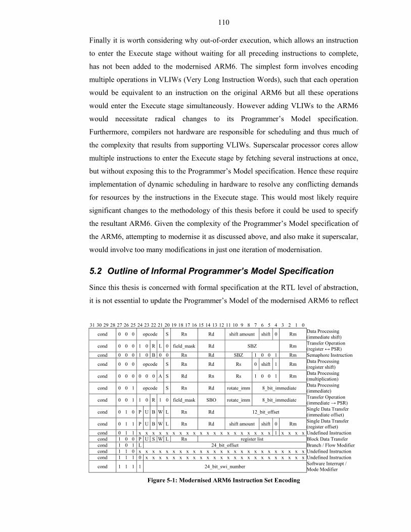
110
Finally it is worth considering why out-of-order execution, which allows an instruction
to enter the Execute stage without waiting for all preceding instructions to complete,
has not been added to the modernised ARM6. The simplest form involves encoding
multiple operations in VLIWs (Very Long Instruction Words), such that each operation
would be equivalent to an instruction on the original ARM6 but all these operations
would enter the Execute stage simultaneously. However adding VLIWs to the ARM6
would necessitate radical changes to its Programmer’s Model specification.
Furthermore, compilers not hardware are responsible for scheduling and thus much of
the complexity that results from supporting VLIWs. Superscalar processor cores allow
multiple instructions to enter the Execute stage by fetching several instructions at once,
but without exposing this to the Programmer’s Model specification. Hence these require
implementation of dynamic scheduling in hardware to resolve any conflicting demands
for resources by the instructions in the Execute stage. This would most likely require
significant changes to the methodology of this thesis before it could be used to specify
the resultant ARM6. Given the complexity of the Programmer’s Model specification of
the ARM6, attempting to modernise it as discussed above, and also make it superscalar,
would involve too many modifications in just one iteration of modernisation.
5.2 Outline of Informal Programmer’s Model Specification
Since this thesis is concerned with formal specification at the RTL level of abstraction,
it is not essential to update the Programmer’s Model of the modernised ARM6 to reflect
31 30 29 28 27 26 25 24 23 22 21 20 19 18 17 16 15 14 13 12 11 10 9 8 7 6 5 4 3 2 1 0
cond 0 0 0 opcode S Rn Rd shift amount shift 0 Rm Data Processing (immediate shift)
cond 0 0 0 1 0 R L 0 field_mask Rd SBZ Rm Transfer Operation (register ↔ PSR)
cond 0 0 0 1 0 B 0 0 Rn Rd SBZ 1 0 0 1 Rm Semaphore Instruction
cond 0 0 0 opcode S Rn Rd Rs 0 shift 1 Rm Data Processing (register shift)
cond 0 0 0 0 0 0 A S Rd Rn Rs 1 0 0 1 Rm Data Processing (multiplication)
cond 0 0 1 opcode S Rn Rd rotate_imm 8_bit_immediate Data Processing (immediate)
cond 0 0 1 1 0 R 1 0 field_mask SBO rotate_imm 8_bit_immediate Transfer Operation (immediate → PSR)
cond 0 1 0 P U B W L Rn Rd 12_bit_offset Single Data Transfer (immediate offset)
cond 0 1 1 P U B W L Rn Rd shift amount shift 0 Rm Single Data Transfer (register offset)
cond 0 1 1 x x x x x x x x x x x x x x x x x x x x 1 x x x x Undefined Instruction cond 1 0 0 P U S W L Rn register list Block Data Transfer cond 1 0 1 L 24_bit_offset Branch / Flow Modifiercond 1 1 0 x x x x x x x x x x x x x x x x x x x x x x x x x Undefined Instruction cond 1 1 1 0 x x x x x x x x x x x x x x x x x x x x x x x x Undefined Instruction
cond 1 1 1 1 24_bit_swi_number Software Interrupt / Mode Modifier
Figure 5-1: Modernised ARM6 Instruction Set Encoding
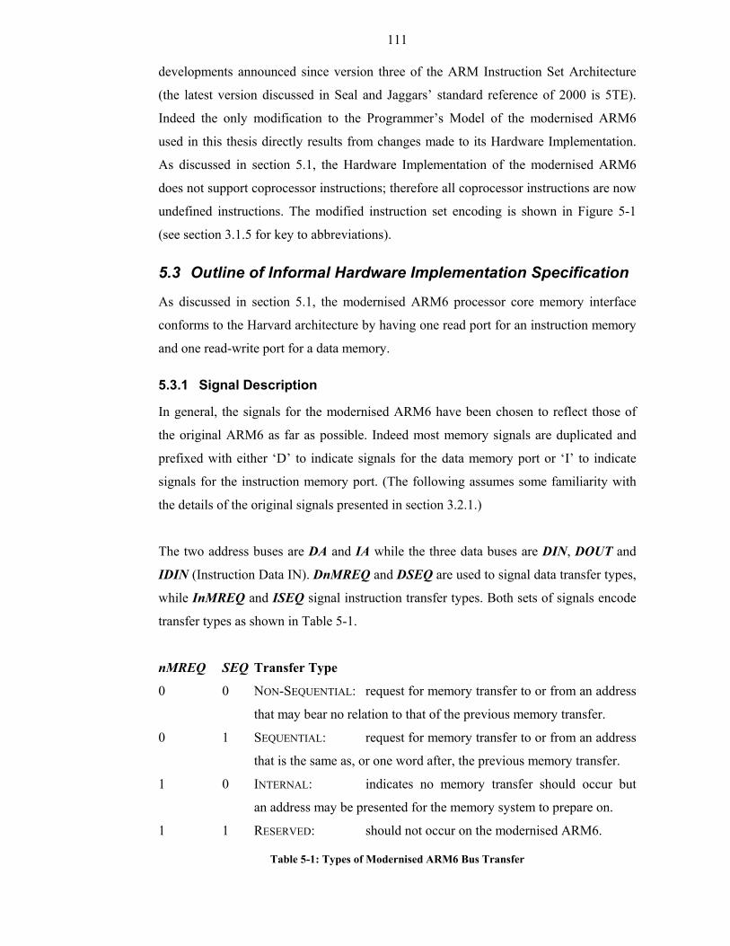
111
developments announced since version three of the ARM Instruction Set Architecture
(the latest version discussed in Seal and Jaggars’ standard reference of 2000 is 5TE).
Indeed the only modification to the Programmer’s Model of the modernised ARM6
used in this thesis directly results from changes made to its Hardware Implementation.
As discussed in section 5.1, the Hardware Implementation of the modernised ARM6
does not support coprocessor instructions; therefore all coprocessor instructions are now
undefined instructions. The modified instruction set encoding is shown in Figure 5-1
(see section 3.1.5 for key to abbreviations).
5.3 Outline of Informal Hardware Implementation Specification
As discussed in section 5.1, the modernised ARM6 processor core memory interface
conforms to the Harvard architecture by having one read port for an instruction memory
and one read-write port for a data memory.
5.3.1 Signal Description
In general, the signals for the modernised ARM6 have been chosen to reflect those of
the original ARM6 as far as possible. Indeed most memory signals are duplicated and
prefixed with either ‘D’ to indicate signals for the data memory port or ‘I’ to indicate
signals for the instruction memory port. (The following assumes some familiarity with
the details of the original signals presented in section 3.2.1.)
The two address buses are DA and IA while the three data buses are DIN, DOUT and
IDIN (Instruction Data IN). DnMREQ and DSEQ are used to signal data transfer types,
while InMREQ and ISEQ signal instruction transfer types. Both sets of signals encode
transfer types as shown in Table 5-1.
nMREQ SEQ Transfer Type
0 0 NON-SEQUENTIAL: request for memory transfer to or from an address
that may bear no relation to that of the previous memory transfer.
0 1 SEQUENTIAL: request for memory transfer to or from an address
that is the same as, or one word after, the previous memory transfer.
1 0 INTERNAL: indicates no memory transfer should occur but
an address may be presented for the memory system to prepare on.
1 1 RESERVED: should not occur on the modernised ARM6.
Table 5-1: Types of Modernised ARM6 Bus Transfer
112
Addressing on the modernised ARM6 processor core is pipelined in the same manner as
the original ARM6 (see section 3.2.1 for details).
The remaining signals involved in transfers with data memory or instruction memory
are defined with reference to the original ARM6 signals as shown in Table 5-2.
ORIGINAL ARM6 MODERNISED ARM6
DATA MEMORY INSTRUCTION MEMORY
ABORT DABORT IABORT
LOCK DLOCK
nBW DnBW
nOPC
nRW DnRW
nTRANS DnTRANS InTRANS
Table 5-2: Equivalents of Modernised ARM6 Memory Signals
The same input signals that reflect the general environment of the original ARM6
(nFIQ, nIRQ and nRESET) are used on the modernised ARM6. The nM output signal
is duplicated as DnM and InM, on the other hand.
5.3.2 Coprocessors
As discussed in section 5.1, the Hardware Implementation of the modernised ARM6
does not support coprocessor instructions; therefore all coprocessor instructions are now
undefined instructions.
5.3.3 Datapath of Processor Core
The modernised ARM6 processor core datapath was designed as depicted in Figure 5-2.
Note the following changes from the datapath of the original ARM6 processor core:
• The modernised ARM6 has an extra register read port RC for reading the value of
the register to be stored in store, store multiple and swap instructions. Likewise it has
an extra register write port WB for writing the value read from memory to the register
to be loaded in load, load multiple and swap instructions.
• While the register read ports operate in φ2 and the register write ports operate in φ1
on the modernised ARM6, the reverse is true for the original ARM6.
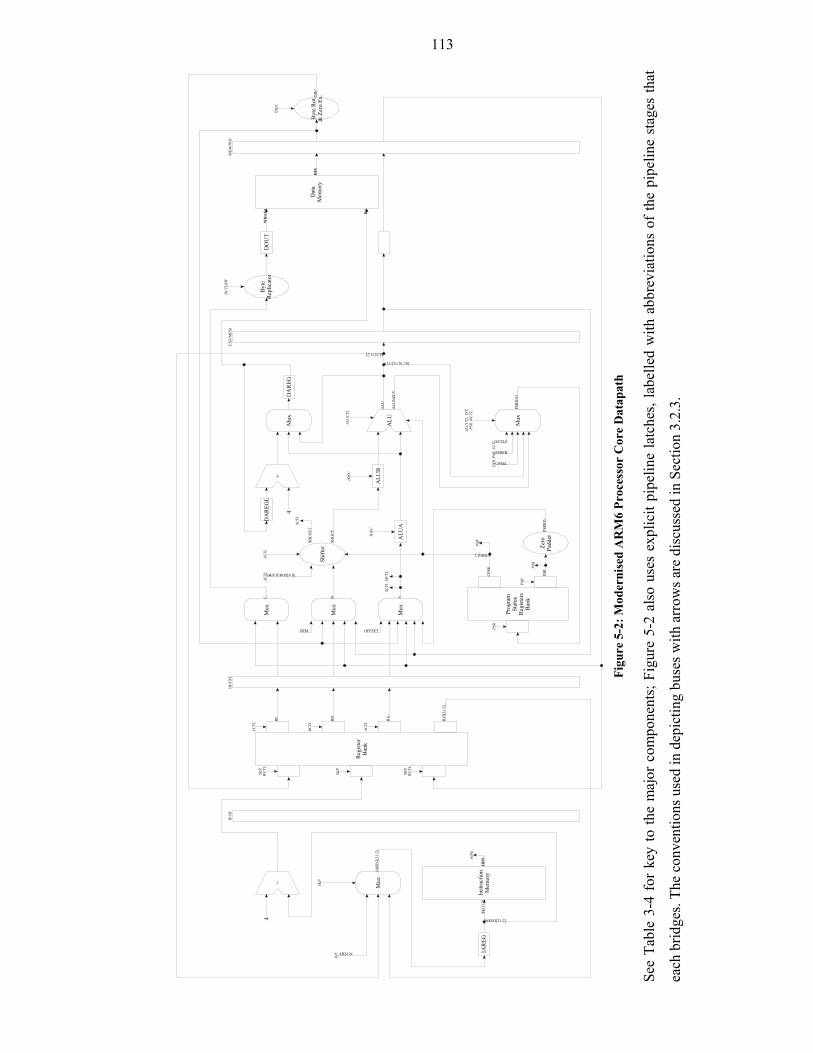
113
Figu
re 5
-2: M
oder
nise
d A
RM
6 Pr
oces
sor
Cor
e D
atap
ath
See
Tabl
e 3-
4 fo
r ke
y to
the
maj
or c
ompo
nent
s; F
igur
e 5-
2 al
so u
ses
expl
icit
pipe
line
latc
hes,
labe
lled
with
abb
revi
atio
ns o
f th
e pi
pelin
e st
ages
that
each
brid
ges.
The
conv
entio
ns u
sed
in d
epic
ting
buse
s with
arr
ows a
re d
iscu
ssed
in S
ectio
n 3.
2.3.
IAR
EG
+
IF/ID
Regi
ster
Ban
k
Prog
ram
Stat
usR
egis
ters
Ban
k
RB
ID/E
XE
Shift
er
RC
ALU
EXE/
MEM
RA
Byte
Rep
licat
or+
4
Byt
e R
ot.
& Z
ero
Ex.
MEM
/WB
Mux
Mux
Mux
Mux
Mux
DA
REG
DIN
’
WD
ATA
Dat
aM
emor
yD
IN
Instr
uctio
nM
emor
yIA
[31:
2]ID
INPIPE
IAR
EG[3
1:2]
AREGN
SKP
INT
SKP
SKP,
WC
TL
SCTLC
PSRFB
CPSRLPSR,
PSR
, SCT
L
Mux
SHC
OU
T
SCTL
ALU[31:26,7:0]
ALU
ALU
NZC
V
Zero
Padd
er
IMM
A
SHIFTEROP[4:0]
ALU
A
ALU
B
PSR
RD
CPSR[C]
PSR
PSR
SCTL
MCT
L
DO
UT
DA
CPS
R
PSR
SHO
UT
ALU
CTL
4
IDEC
IDEC
DC
TLBW
IDEC
ACTL
BCTL
CCTL
PSR
PSR
PSRD
AT
IAREG[31:2]
R15
[31:
2]
DA
REG
L
BC
OFFSET
ALU[31:2]
ALU
CTL,
INT,
PSR,
WC
TL
SKP,
WC
TLSC
TLSC
TL
114
• The modernised ARM6 cannot use one incrementer for sequential fetches from
instruction addresses and data addresses; it requires separate incrementers for each.
• Register reads are performed one clock cycle earlier than on the original ARM6:
read ports RA and RB operate in the Instruction Decode stage not the Execute stage.
Although read port RC operates in the Execute stage, its operation is not equivalent
to that of read ports RA and RB on the original ARM6 because its value is not used
until the Memory stage.
• To ensure backwards compatibility, if PC refers to the address of the instruction in
the Execute stage, if the value of the program counter is used in the first iteration of
the instruction in the Execute stage, its value must equal PC + 8; otherwise its value
must equal PC + 12. Hence, the instruction incrementer is used to calculate in tn φ1
the sequential instruction address for tn φ2 rather than in tn - 1 φ2, so that if it is used
to update the program counter, it is always one clock cycle ahead.
• Since results are not stored in destination registers (except for the program counter)
until writeback, forwarding of values is required such that following instructions that
use the results before writeback occurs get the right values and these instructions stall
only if the result has not been read from memory (see section 5.3.4 for more details).
• Byte rotation and zero padding, as appropriate, of the value read from memory in
load and swap instructions is implemented in a specialized functional unit rather than
the barrel shifter.
5.3.4 Control Subsystem of Processor Core
The activities performed by the modernised ARM6 divide into five pipelined stages:
1. INSTRUCTION FETCH: latches the instruction, if any, fetched from instruction memory
in reply to signals presented to instruction memory in the previous clock cycle and,
if appropriate, presents signals to fetch an instruction in the next clock cycle.
2. INSTRUCTION DECODE: decodes the instruction for execution in the next clock cycle
(if the current instruction in the execute stage only needs one more clock cycle then
the next instruction is decoded, or else decode of the current instruction continues)
and reads any relevant registers.
3. EXECUTE: performs appropriate calculations and, if appropriate, presents signals
to data memory to prepare an access in the next clock cycle. This may take more than
one clock cycle.
115
4. MEMORY: if appropriate, performs access involving data memory.
5. WRITEBACK: if appropriate, writes the results to pertinent registers.
Note, as on the original ARM6, fetch activities occur for the first and the last clock cycle
an instruction is in the Execute stage. Furthermore the same number of latches is used
to store instructions in the pipeline, since it is more efficient to pipeline pertinent results
from primary decode in the Decode stage, and secondary decode in the Execute stage,
for both the Memory stage and the Writeback stage than perform any further decode.
The control subsystem of the modernised ARM6 was designed to preserve as much of
that of the original ARM6 as possible and thus also the commercial principles of design
that underlie it. Nevertheless, full advantage was taken of the opportunities provided by
using a five stage pipeline rather than a three stage pipeline for simplifying aspects of
the control subsystem. For example, on the original ARM6 the registers involved in
the transfers made by load multiple or store multiple instructions are specially buffered
for one or two clock cycles before being used. However, on the modernised ARM6,
these registers may be buffered in the same manner as any other signals required for
the Memory stage or the Writeback stage without special considerations.
Since the modernised ARM6, unlike the original ARM6, performs register reads,
register writes and memory operations in different pipeline stages, certain data hazards
need to be resolved on the modernised ARM6 that do not apply to the original ARM6.
This necessitates additional control logic as summarised in Table 5-3.
Read After Write
Data Hazard An instruction that performs its final iteration in the Execute stage at tn
may not write the result of its calculations into its destination register
until tn + 2. Similarly if it reads from data memory in the Memory stage
at tn + 1, writeback of the resulting value does not occur until tn + 2.
Therefore if the instructions that enter the Execute stage at either tn + 1
or tn + 2 need either of these results, the relevant register cannot be read
as usual in the corresponding Instruction Decode stage (tn or tn + 1).
116
Resolution In general, forwarding logic is used so that, irrespective of the value
read at tn or tn + 1, the A, B or C multiplexers can select the correct value
at tn + 1 and tn + 2. However, values read from memory are not available
until tn + 2 and cannot be forwarded even then if byte rotation is required.
Consequently, an instruction that requires the memory value at tn + 1
must be interlocked in the Instruction Decode stage for one clock cycle
when forwarding is possible and two when it is not. (An instruction that
requires the memory value at tn + 2 must be interlocked one clock cycle,
if forwarding is not possible.) Note that store multiple instructions and
store instructions read the register to be stored in the Execute stage
rather than the Instruction Decode stage. Thus, should such instructions
require the use of the memory value at tn + 1 for the register to be stored,
the instructions must interlock in the Execute stage for one clock cycle.
(This cannot be detected and dealt with in the Instruction Decode stage,
since the register to be read is not determined until the Execute stage.)
Data Hazard A store multiple instruction that stores the base register to memory
and updates it, stores the updated value unless the base register is R0.
This proves problematic because the original ARM6 also does not store
the updated value if the base register is R1 and its Programmer’s Model
exposes this behaviour.
Resolution These instructions are of limited use, so the complications involved in
making the modernised ARM6 behave as the Programmer’s Model for
the original ARM6 are not worthwhile. Hence, use of such instructions
on the modernised ARM6 is deprecated.
Write After Write
Data Hazard A load instruction or load multiple instruction can be constructed that
attempts to update the base register with a value read from memory in
the same clock cycle as it should be updated with the new base address.
Resolution These instructions serve little purpose; so rather than specify which of
the two writes should prevail, the use of such instructions is deprecated.
(Note behaviour for load multiple instructions that load the base register
from memory and update the base register with the new base address,
but not in the same clock cycle, differs between the original ARM6 and
the modernised ARM6. Hence these instructions are also deprecated.)
117
Data Hazard The dedicated write port for updating the program counter with a value
from the incrementer and both the general-purpose write ports operate
at the same time.
Resolution The data hazard can only occur if the dedicated write port operates
when one of the others updates the program counter, but the measures
discussed below for preventing control hazards also prevent this hazard.
Table 5-3: Data Hazards of Modernised ARM6
Implementing the behaviours required by the Programmer’s Model of the ARM6 for
each instruction using the datapath of the original ARM6 necessitates the resolution of
several structural hazards. In most cases the limitations of its three stage pipeline and
the von Neumann architecture of its memory interface necessitate several iterations in
the Execute stage for the instructions that would generate such hazards. These hazards
arise when the resources required of the datapath to implement certain behaviours in
one clock cycle exceed those available. Hence such hazards can often be resolved,
without requiring any extra iterations in the Execute stage for the effected instructions,
by assigning the behaviours in contention to different but already required iterations.
However the preceding approach to the resolution of structural hazards in the design of
the original ARM6 is less effective with respect to the design of the modernised ARM6,
Status in Design of Structural Hazard
Original ARM6 Modernised ARM6
Simultaneous writeback of updated base
and value loaded from memory.
(Effects: loads; load multiples.)
Writeback split over
two clock cycles.
Two write ports so
hazard does not apply.
Processing the value to store to memory
at the same time as the A and B buses
are used in preparing inputs for ALU.
(Effects: stores; store multiples; swaps.)
Dataflow split across
two clock cycles
(needs introduction of
extra cycle for swaps).
Independent read port
and dataflow for value
to store to memory so
hazard does not apply.
Simultaneous access of data memory
and instruction memory.
(Effects: loads; load multiples; stores;
store multiples; swaps.)
Accesses split over
two clock cycles.
Two incrementers and
two memory ports so
hazard does not apply
(the data memory port
is read-write).
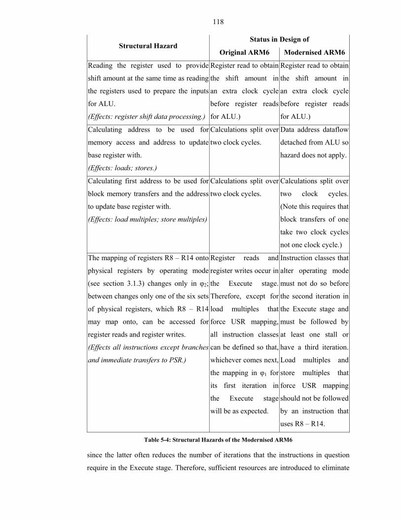
118
Status in Design of Structural Hazard
Original ARM6 Modernised ARM6
Reading the register used to provide
shift amount at the same time as reading
the registers used to prepare the inputs
for ALU.
(Effects: register shift data processing.)
Register read to obtain
the shift amount in
an extra clock cycle
before register reads
for ALU.)
Register read to obtain
the shift amount in
an extra clock cycle
before register reads
for ALU.)
Calculating address to be used for
memory access and address to update
base register with.
(Effects: loads; stores.)
Calculations split over
two clock cycles.
Data address dataflow
detached from ALU so
hazard does not apply.
Calculating first address to be used for
block memory transfers and the address
to update base register with.
(Effects: load multiples; store multiples)
Calculations split over
two clock cycles.
Calculations split over
two clock cycles.
(Note this requires that
block transfers of one
take two clock cycles
not one clock cycle.)
The mapping of registers R8 – R14 onto
physical registers by operating mode
(see section 3.1.3) changes only in φ2;
between changes only one of the six sets
of physical registers, which R8 – R14
may map onto, can be accessed for
register reads and register writes.
(Effects all instructions except branches
and immediate transfers to PSR.)
Register reads and
register writes occur in
the Execute stage.
Therefore, except for
load multiples that
force USR mapping,
all instruction classes
can be defined so that,
whichever comes next,
the mapping in φ1 for
its first iteration in
the Execute stage
will be as expected.
Instruction classes that
alter operating mode
must not do so before
the second iteration in
the Execute stage and
must be followed by
at least one stall or
have a third iteration.
Load multiples and
store multiples that
force USR mapping
should not be followed
by an instruction that
uses R8 – R14.
Table 5-4: Structural Hazards of the Modernised ARM6
since the latter often reduces the number of iterations that the instructions in question
require in the Execute stage. Therefore, sufficient resources are introduced to eliminate
119
particular structural hazards in the design of the modernised ARM6 altogether,
whenever the reduction in the number of iterations needed outweighs the complexity of
the logic involved.
The nature of the Pre-fetch queue of the modernised ARM6 has not changed from that
of the original ARM6. In general, instruction classes that alter the program counter on
the modernised ARM6 do so via the IAREG[31:2] bus and the address incrementer in
the Execute stage, without waiting until the instruction class enters the Writeback stage.
Hence the control hazards in the design of the original ARM6 still apply to the design of
the modernised ARM6 and are most significant in the latter. Other control hazards
also apply to the latter design and involve load instructions or load multiple instructions
in which the program counter is one of the register destinations. Such instructions
cannot update the program counter until the Writeback stage, as neither the new value
nor the data abort status can be obtained before this stage. Hence the same resolution as
on the original ARM6 can be used for all control hazards—flushing the Pre-fetch queue
and refilling it with valid instructions—but those involving program counter changes in
the Writeback stage also require the Pre-fetch queue to be interlocked until writeback to
the program counter occurs.
5.4 Summary
The modernised ARM6 was designed to implement, except for coprocessor instructions,
the same Programmer’s Model specification as the original ARM6. The main change in
the implementation involved using a Harvard architecture with a five stage pipeline
rather than a von Neumann architecture with a three stage pipeline. Indeed a number of
other changes, such as the addition of forwarding logic, were a direct consequence of
reconciling this change with the desire for backwards compatibility. Still, apart from
certain modifications necessary to implement these changes, the control subsystem of
the modernised ARM6 is little changed from that of the original ARM6. Not all changes
were associated with an increase in complexity of the design: the deeper pipelining of
the modernised ARM6 facilitated simplification of certain aspects (for example,
calculating when each of the registers involved in a block data transfer should be loaded
or stored).
120
6 Specifying a Modernised ARM6 To demonstrate that it is possible to use the methodology developed for this thesis with
modern processor designs, the methodology was used to specify the modernised ARM6
introduced in section 5. Section 6.1 outlines what the resultant specification involved;
while section 6.2, section 6.3 and section 6.4 relate how it was developed in respect of
each of the three presentations used with this specification (see section 2.3 for details on
the method underlying each presentation).
The methodology of this thesis was reasonably mature when it was applied to creating
a Phase specification of the modernised ARM6, thus it was decided that the design
would be developed using this specification instead of being constructed beforehand.
This decision was taken in order to demonstrate that the methodology of this thesis
could be used as part of the design process itself, not just when the design is complete
(as with the original ARM6 and all but a few details of the DLX and the MIPS R2000—
see section 7).
6.1 General Principles
The scope of the specification of the modernised ARM6 is noticeably different to that of
the original ARM6 in some respects. For example, while coprocessor instruction classes
were required for specification of the original ARM6 and not the modernised ARM6,
specification of the modernised ARM6, unlike that of the original ARM6, must consider
the Memory and the Writeback pipeline activities. Although such differences as these
were simply inferred from the modifications used to create the modernised ARM6,
others were only discovered in the process of producing the Phase specification itself.
For instance, to specify interlock handling on the modernised ARM6, it was necessary
to define an instruction class for interlocking other instruction classes in the pipeline,
while on the original ARM6 a description of the pipeline control logic and the nature of
the instruction classes that could interlock, was sufficient.
The following instruction classes were used to specify the modernised ARM6:
• CONTROL INSTRUCTIONS
♦ br: encapsulates flow modifiers (see section 3.1.4).
♦ swi_ex: encapsulates mode modifiers (see section 3.1.4) and exceptions raised by
external events (see section 3.1.2) such as interrupts and memory aborts.
121
• DATA PROCESSING OPERATIONS
♦ data_proc: encapsulates arithmetic operations, data register transfer operations
and logical operations (see section 3.1.4) with immediates or immediate shifts
(see section 3.1.5).
♦ mla_mul: encapsulates multiplication operations (see section 3.1.4).
♦ mrs_msr: encapsulates transfer operations involving the program status registers
(see section 3.1.4).
♦ reg_shift: encapsulates arithmetic operations, data register transfer operations and
logical operations (see section 3.1.4) with register shifts (see section 3.1.5).
• MEMORY INSTRUCTIONS
♦ ldm: encapsulates block data transfers from memory to the modernised ARM6
(see section 3.1.4).
♦ ldr: encapsulates single data transfers from memory to the modernised ARM6
(see section 3.1.4).
♦ stm: encapsulates block data transfers from the modernised ARM6 to memory
(see section 3.1.4).
♦ str: encapsulates single data transfers from the modernised ARM6 to memory
(see section 3.1.4).
♦ swp: encapsulates semaphore instructions (see section 3.1.4).
• INSTRUCTION SET EXTENDERS
♦ und: encapsulates undefined instructions (see section 3.1.4). Note Figure 5-1,
rather than Figure 3-2, defines the associated instruction encodings.
• NULL INSTRUCTIONS
♦ stall: inserted by pipeline control logic in the Execute stage, in order to interlock
the instruction class in the Instruction Decode stage.
♦ unexec: substituted for the instruction class that would otherwise have entered
the Execute stage when the pipeline control logic detects that the instruction class
failed its condition code (see section 3.1.4).
This list of instruction classes is very similar to that given for the original ARM6 in
section 4.1, which is unsurprising since the modernised ARM6 was designed to support
the same Instruction Set Architecture as the original ARM6, except for the support of
coprocessor instructions (see section 5.1). Indeed the subsumption of instruction classes
concerning coprocessors into the undefined instruction class (cdp_und is renamed und
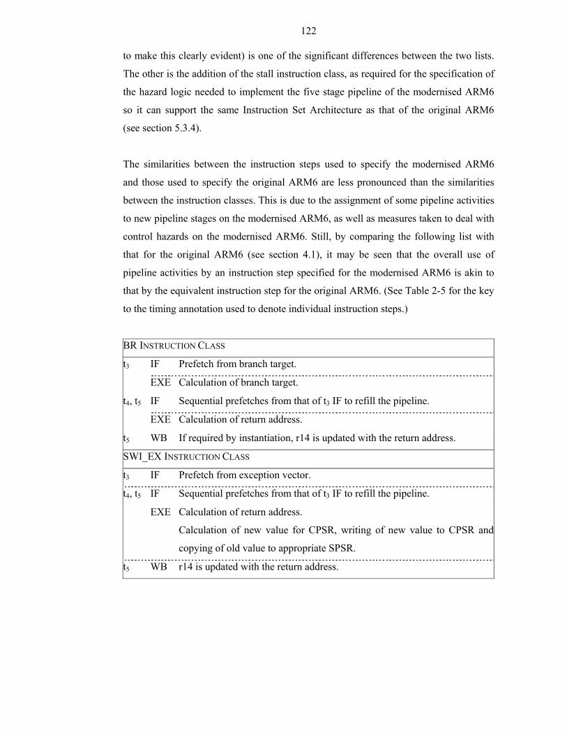
122
to make this clearly evident) is one of the significant differences between the two lists.
The other is the addition of the stall instruction class, as required for the specification of
the hazard logic needed to implement the five stage pipeline of the modernised ARM6
so it can support the same Instruction Set Architecture as that of the original ARM6
(see section 5.3.4).
The similarities between the instruction steps used to specify the modernised ARM6
and those used to specify the original ARM6 are less pronounced than the similarities
between the instruction classes. This is due to the assignment of some pipeline activities
to new pipeline stages on the modernised ARM6, as well as measures taken to deal with
control hazards on the modernised ARM6. Still, by comparing the following list with
that for the original ARM6 (see section 4.1), it may be seen that the overall use of
pipeline activities by an instruction step specified for the modernised ARM6 is akin to
that by the equivalent instruction step for the original ARM6. (See Table 2-5 for the key
to the timing annotation used to denote individual instruction steps.)
BR INSTRUCTION CLASS
t3 IF Prefetch from branch target.
EXE Calculation of branch target.
t4, t5 IF Sequential prefetches from that of t3 IF to refill the pipeline.
EXE Calculation of return address.
t5 WB If required by instantiation, r14 is updated with the return address.
SWI_EX INSTRUCTION CLASS
t3 IF Prefetch from exception vector.
t4, t5 IF Sequential prefetches from that of t3 IF to refill the pipeline.
EXE Calculation of return address.
Calculation of new value for CPSR, writing of new value to CPSR and
copying of old value to appropriate SPSR.
t5 WB r14 is updated with the return address.
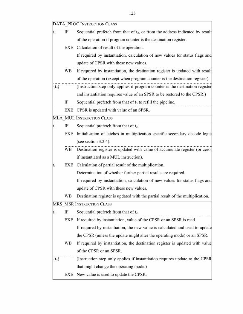
123
DATA_PROC INSTRUCTION CLASS
t3 IF Sequential prefetch from that of t2, or from the address indicated by result
of the operation if program counter is the destination register.
EXE Calculation of result of the operation.
If required by instantiation, calculation of new values for status flags and
update of CPSR with these new values.
WB If required by instantiation, the destination register is updated with result
of the operation (except when program counter is the destination register).
{t4} (Instruction step only applies if program counter is the destination register
and instantiation requires value of an SPSR to be restored to the CPSR.)
IF Sequential prefetch from that of t3 to refill the pipeline.
EXE CPSR is updated with value of an SPSR.
MLA_MUL INSTRUCTION CLASS
t3 IF Sequential prefetch from that of t2.
EXE Initialisation of latches in multiplication specific secondary decode logic
(see section 3.2.4).
WB Destination register is updated with value of accumulate register (or zero,
if instantiated as a MUL instruction).
tn EXE Calculation of partial result of the multiplication.
Determination of whether further partial results are required.
If required by instantiation, calculation of new values for status flags and
update of CPSR with these new values.
WB Destination register is updated with the partial result of the multiplication.
MRS_MSR INSTRUCTION CLASS
t3 IF Sequential prefetch from that of t2.
EXE If required by instantiation, value of the CPSR or an SPSR is read.
If required by instantiation, the new value is calculated and used to update
the CPSR (unless the update might alter the operating mode) or an SPSR.
WB If required by instantiation, the destination register is updated with value
of the CPSR or an SPSR.
{t4} (Instruction step only applies if instantiation requires update to the CPSR
that might change the operating mode.)
EXE New value is used to update the CPSR.
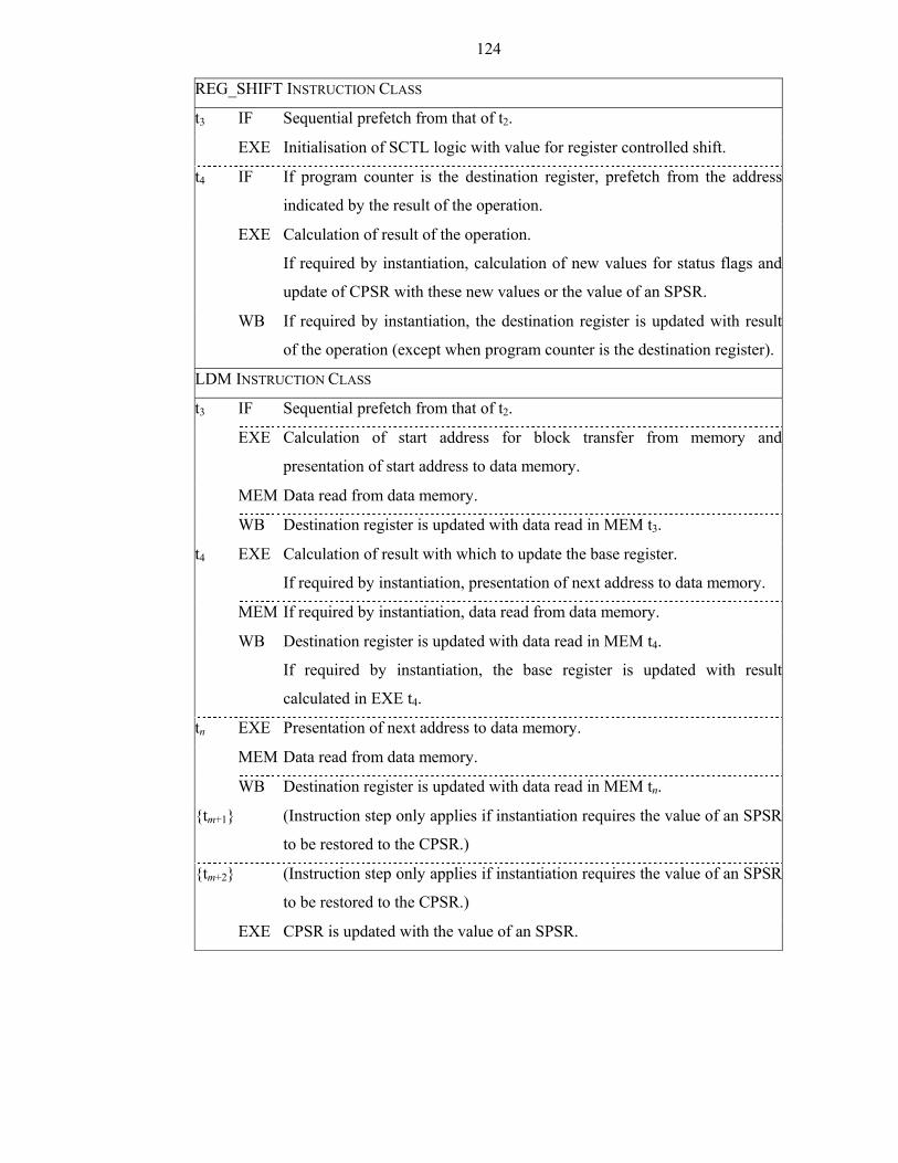
124
REG_SHIFT INSTRUCTION CLASS
t3 IF Sequential prefetch from that of t2.
EXE Initialisation of SCTL logic with value for register controlled shift.
t4 IF If program counter is the destination register, prefetch from the address
indicated by the result of the operation.
EXE Calculation of result of the operation.
If required by instantiation, calculation of new values for status flags and
update of CPSR with these new values or the value of an SPSR.
WB If required by instantiation, the destination register is updated with result
of the operation (except when program counter is the destination register).
LDM INSTRUCTION CLASS
t3 IF Sequential prefetch from that of t2.
EXE Calculation of start address for block transfer from memory and
presentation of start address to data memory.
MEM Data read from data memory.
WB Destination register is updated with data read in MEM t3.
t4 EXE Calculation of result with which to update the base register.
If required by instantiation, presentation of next address to data memory.
MEM If required by instantiation, data read from data memory.
WB Destination register is updated with data read in MEM t4.
If required by instantiation, the base register is updated with result
calculated in EXE t4.
tn EXE Presentation of next address to data memory.
MEM Data read from data memory.
WB Destination register is updated with data read in MEM tn.
{tm+1} (Instruction step only applies if instantiation requires the value of an SPSR
to be restored to the CPSR.)
{tm+2} (Instruction step only applies if instantiation requires the value of an SPSR
to be restored to the CPSR.)
EXE CPSR is updated with the value of an SPSR.
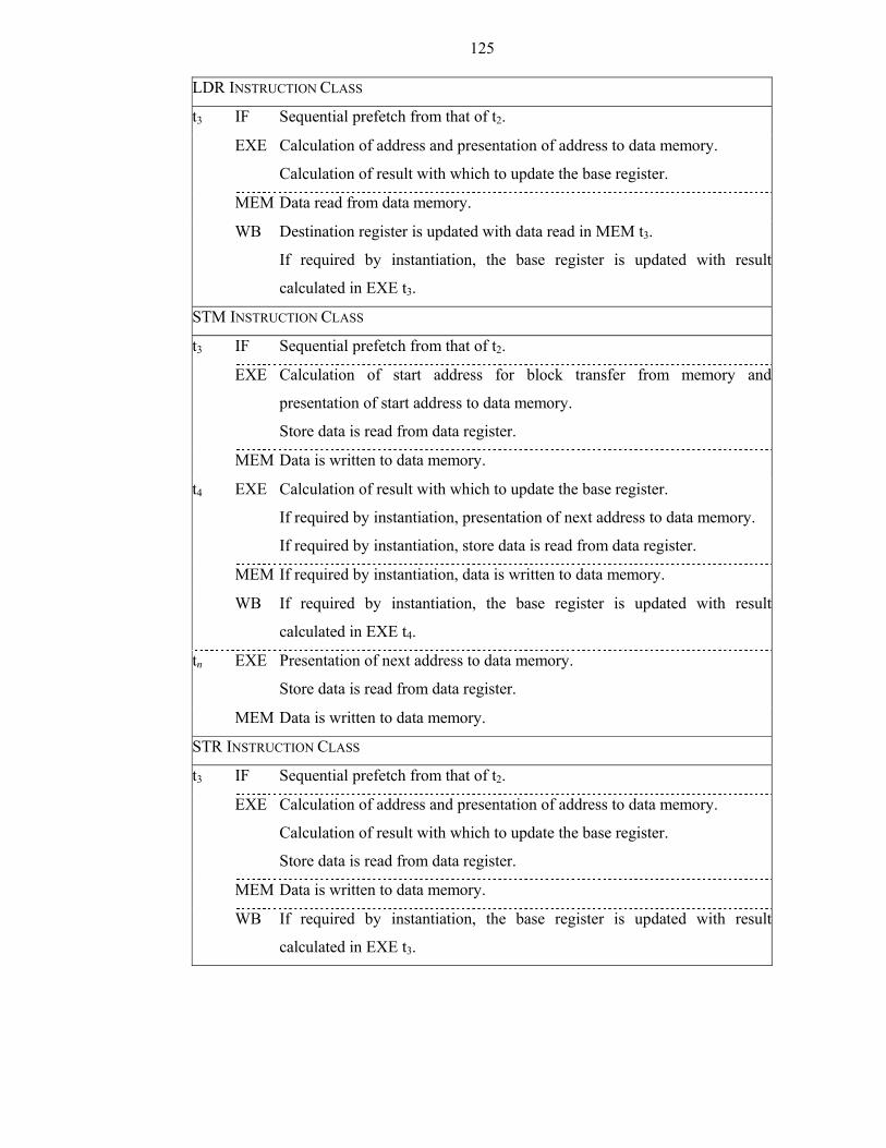
125
LDR INSTRUCTION CLASS
t3 IF Sequential prefetch from that of t2.
EXE Calculation of address and presentation of address to data memory.
Calculation of result with which to update the base register.
MEM Data read from data memory.
WB Destination register is updated with data read in MEM t3.
If required by instantiation, the base register is updated with result
calculated in EXE t3.
STM INSTRUCTION CLASS
t3 IF Sequential prefetch from that of t2.
EXE Calculation of start address for block transfer from memory and
presentation of start address to data memory.
Store data is read from data register.
MEM Data is written to data memory.
t4 EXE Calculation of result with which to update the base register.
If required by instantiation, presentation of next address to data memory.
If required by instantiation, store data is read from data register.
MEM If required by instantiation, data is written to data memory.
WB If required by instantiation, the base register is updated with result
calculated in EXE t4.
tn EXE Presentation of next address to data memory.
Store data is read from data register.
MEM Data is written to data memory.
STR INSTRUCTION CLASS
t3 IF Sequential prefetch from that of t2.
EXE Calculation of address and presentation of address to data memory.
Calculation of result with which to update the base register.
Store data is read from data register.
MEM Data is written to data memory.
WB If required by instantiation, the base register is updated with result
calculated in EXE t3.
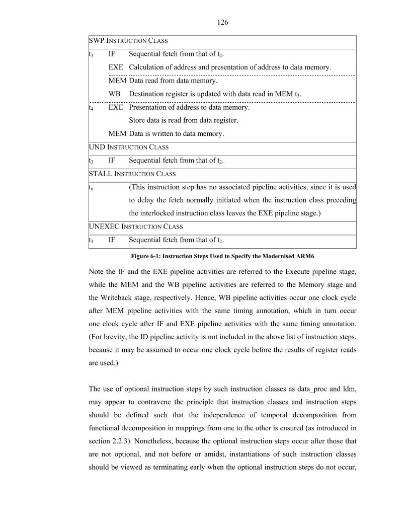
126
SWP INSTRUCTION CLASS
t3 IF Sequential fetch from that of t2.
EXE Calculation of address and presentation of address to data memory.
MEM Data read from data memory.
WB Destination register is updated with data read in MEM t3.
t4 EXE Presentation of address to data memory.
Store data is read from data register.
MEM Data is written to data memory.
UND INSTRUCTION CLASS
t3 IF Sequential fetch from that of t2.
STALL INSTRUCTION CLASS
tn (This instruction step has no associated pipeline activities, since it is used
to delay the fetch normally initiated when the instruction class preceding
the interlocked instruction class leaves the EXE pipeline stage.)
UNEXEC INSTRUCTION CLASS
t3 IF Sequential fetch from that of t2.
Figure 6-1: Instruction Steps Used to Specify the Modernised ARM6
Note the IF and the EXE pipeline activities are referred to the Execute pipeline stage,
while the MEM and the WB pipeline activities are referred to the Memory stage and
the Writeback stage, respectively. Hence, WB pipeline activities occur one clock cycle
after MEM pipeline activities with the same timing annotation, which in turn occur
one clock cycle after IF and EXE pipeline activities with the same timing annotation.
(For brevity, the ID pipeline activity is not included in the above list of instruction steps,
because it may be assumed to occur one clock cycle before the results of register reads
are used.)
The use of optional instruction steps by such instruction classes as data_proc and ldm,
may appear to contravene the principle that instruction classes and instruction steps
should be defined such that the independence of temporal decomposition from
functional decomposition in mappings from one to the other is ensured (as introduced in
section 2.2.3). Nonetheless, because the optional instruction steps occur after those that
are not optional, and not before or amidst, instantiations of such instruction classes
should be viewed as terminating early when the optional instruction steps do not occur,
127
instead of having a significantly different function (in the same way the number of
iterations performed for one instruction step does not matter).
6.2 Mathematical Presentation
As already noted in section 6, the methodology of this thesis was well developed when
it was applied to the modernised ARM6. Consequently, although some modifications
were required to the methodology in order to create the mathematical presentation of
the modernised ARM6, none of these necessitated respecification. This contrasts with
the specification of the original ARM6, which involved two separate attempts to create
the mathematical presentation before the final successful attempt (see section 4.2).
The first modification made to the methodology was the introduction of notation for
pipeline latches discussed in section 2.3.1, to avoid the need to explicitly name signals
buffered from previous pipeline stages. For example, it is evident from Figure 5-2 that
the value on the ALU bus in the Execute stage may be used in both the Memory stage
and the Writeback stage. This could be handled by explicitly specifying that:
2ALUMEM1 ALUϕ← such that the bus driven by ALUMEM1 in
MEM φ1 can be used to access the value that
was driven on the ALU bus in EXE φ2.
1ALUMEM2 ALUMEM1ϕ← such that the bus driven by ALUMEM2 in
MEM φ2 can be used to access the value that
was driven on the ALU bus in EXE φ2.
2ALUWB1 ALUMEM2ϕ← such that the bus driven by ALUWB1 in
WB φ1 can be used to access the value that
was driven on the ALU bus in EXE φ2.
However, it is simpler and clearer to refer to [ ]EXE MEM ALU instead of ALUMEM1
or ALUMEM2 (whether buffering from MEM φ1 to MEM φ2 is required is left implicit,
as it may be inferred from the context) and [ ]MEM WB ALU rather than ALUWB1.
The specification of the original ARM6 defined types to package together the signals
used to drive register read ports and register write ports. For instance:
128
( )n 1000, USR register read from the user operating mode r8
( )( )true, n 1000, USR register write is enabled to the user operating mode r8
where n(x, y) is a function used to explicitly map a virtual reference ‘x’, using a bank
select signal ‘y’, onto a physical register in the appropriate bank of physical registers.
Each register port was specified as driven by one abstract signal, which as shown above,
either referenced an invocation of n(x, y), if it was a read port, or a pair of an invocation
and a Boolean value to indicate if a write should occur, if it was a write port.
Although this provides convenient abstractions for use in describing how register banks
perform register operations, the modernised ARM6 uses the signals pertaining to
register operations for other purposes. For example, the register write for data read from
data memory is scheduled in the Execute stage but is performed in the Writeback stage.
As the write enable signal is buffered across the pipeline stages, it may be forced low
due to a data abort. Furthermore, to specify the forwarding logic, the write enable signal
and the write address signal must be examined independently. Since the specification of
the register bank must decompose the port signal union types, repeated decomposition
could be reduced by specifying the forwarding logic as part of the register bank.
However, this would invalidate the assumption of the methodology of this thesis that
components such as register banks are readily reusable between processor cores and
may be verified independently of particular processor cores. Therefore, it was decided
to treat each of the signals in the specification of the modernised ARM6 that relate to
register operations as separate and furthermore not to include packaging together signals
for register reads and for register writes in the discussion of the general methodology of
this thesis in section 2.3.1.
The forwarding logic is also specified separately from the A, B and C multiplexers,
rather than with direct selection of the forwarding path by the appropriate multiplexer,
as shown in Figure 5-2. A forward bus and a forward enable are specified for each of
the three multiplexers: the forward bus is driven with the value of the forwarding path
while the forward enable indicates whether the value on the forward bus should be used
in preference to the value on the bus from the register read port. (When the multiplexer
would select the immediate bus instead of the bus from the register read port anyway,
for example, the forward enable is ignored.) Specifying the forwarding logic in this way
129
simplifies the specification of the A, B and C multiplexers, as well as allowing
forwarding logic to be specified as part of the pipeline control specification instead of
as part of the datapath control specification. (The A, B and C multiplexers are specified
as part of the datapath control specification, as each instruction class may select inputs
using different criteria, but forwarding logic is not dependent on instruction class and
thus specifying it as part of the datapath control specification would involve
unnecessary duplication across instruction classes.)
The forward bus and the forward enable of each multiplexer are not packaged together,
for the same reasons that the write enable signal and the write address signal are not.
However, in both cases it is convenient to specify one function that calculates both of
the signals, rather than repeat the same calculations in two functions. This is denoted by
defining a function with an n-tuple of names as well as an n-tuple of results rather than
one name and one result; for example:
( )RWAA,RWAEN2
f 1110,1
=
the logic drives 14 onto RWAA[3:0] and 1 onto RWAEN2[0]
As discussed in section 5.3.4, the modernised ARM6 has data hazards that do not affect
the original ARM6 and which, in certain circumstances, can only be overcome by
interlocking effected instructions in the Instruction Decode stage or the Execute stage.
Such data hazards are the result of the interaction of two instructions in the pipeline,
and thus cannot be described in terms of the pipeline activities of one instruction class.
Therefore, the logic responsible for detecting the data hazards that require an instruction
to interlock in the pipeline was specified as part of the pipeline control specification,
instead of as part of the datapath control specification. The imposition of an interlock in
the Instruction Decode stage is also fully described by the pipeline control specification,
as it is handled by inserting the stall instruction class into the Execute stage to prevent
the affected instruction class from leaving the Instruction Decode stage and entering it.
By contrast, just the pipeline control specification cannot be used to describe how
instruction classes interlock in the Execute stage, as the datapath control specification of
the effected instruction class will assign it pipeline activities that have effects visible at
the level of abstraction of the Programmer’s Model specification (such as indicating that
a store will occur in the next clock cycle). Hence, the pipeline control specification
130
describes how an instruction class interlocked in the Execute stage is prevented from
progressing to its next instruction step, whereas its datapath control specification
indicates how the pipeline activities associated with it are prevented from having effects
visible at the level of abstraction of the Programmer’s Model specification.
Both structural hazards and control hazards can be described in terms of the results of
the pipeline activities of one instruction class. Consequently, in most cases the logic that
resolves these hazards is just described as part of the datapath control specification of
the effected instruction class. However, in some cases such as a load instruction with
the program counter as the destination register or the base register when base writeback
is enabled, it is convenient to use the mechanism for interlocking instruction classes in
the Instruction Decode stage to stall the instructions that succeed the load instruction
until the pipeline can be flushed. (The discussion of the use of pipeline flushes to handle
control hazards in section 4.2 also applies to the modernised ARM6, because it uses
pipeline flushes in the same way as the original ARM6.)
For the most part, the logic required to handle exceptions, and thus the functions used to
specify it, is the same for the original ARM6 and the modernised ARM6, since both
support the same exceptions and handle these exceptions in the Execute pipeline stage.
The modernised ARM6 does not support coprocessor instructions, but still handles
undefined instructions as if these were instructions that every coprocessor must reject in
the Execute stage except that the rejection occurs without reference to CPA or CPB
(see section 3.2.2). Conversely, the modernised ARM6 compared to the original ARM6
has an added complication in how data aborts are handled: the abort may occur when
the instruction that performed the memory access is no longer in the Execute stage
(because an instruction enters the Memory stage to perform its final memory access).
This is resolved by substituting the unexec instruction class for that of the instruction in
the Execute stage when a data abort is detected the clock phase after an instruction left
the Execute stage (when that instruction is in the Memory stage). The substitution
occurs in φ2 rather than φ1 so that the timing of the abort signal is not made critical for
the pipeline control logic. However to make the substitution in φ2, the value of IC[*]
must be calculated anew for φ2 instead of just latched from φ1. (Note that substitution
could be avoided by modifying the relevant functions of every instruction class so that
transfers that have effects visible at the level of the Programmer’s Model specification
are prevented directly. However, this solution was not used because it would diminish
131
the abstraction provided by instruction classes, since these modifications are related to
interactions in the pipeline rather than the instruction class being specified.)
The final change required in the application of the methodology of this thesis to create
the mathematical presentation of the modernised ARM6 relates to how primary decode
is performed. The original ARM6 used two PLAs to perform primary decode: a fast one
with a small number of inputs to calculate only the register read port addressing signals
and a standard one for calculating all the other control signals. This is not mentioned in
section 3 or section 4, because the implementation of the original ARM6 separated
primary decode into two PLAs to improve the timing of its critical path. The choice of
two PLAs instead of one thus relates to facilitating a particular implementation strategy,
instead of providing behaviour required by the design. However, the modernised ARM6
does require two PLAs, since the calculation of the register read port addressing signals
is based on which instruction class should enter (or iterate) in the Execute stage,
and calculation of this involves signals that indicate whether an interlock should occur
because of the register read port addressing signals. This interdependency is resolved by
using a fast PLA to calculate the register read port addressing signals on the assumption
the instruction class in the Instruction Decode stage is not pre-empted by an exception
or interlocked. The standard PLA can then calculate all the other control signals
according to which instruction class actually enters (or iterates) in the Execute stage,
since the signals that indicate whether an interlock should occur can use the results of
the fast PLA. (It does not matter that the fast PLA may lead to incorrect register reads
when an interlock or an exception occurs, because in both these cases the register reads
will not have effects visible at the level of the Programmer’s Model specification.)
The NXTIC function abstracts over primary decode by decoding the instruction class
instantiated by an instruction (see section 2.3.1), thus to define NXTIC twice—once for
each PLA—in the mathematical specification would involve significant duplication
without really reflecting the distinction between the two PLAs. Therefore the need for
two PLAs is simply noted when the NXTIC function is defined: the actual parameters of
the standard PLA are specified in the definition while those that would be different for
the fast PLA are specified in the note.
132
6.3 Engineering Presentation
The engineering presentation of the formal specification of the modernised ARM6
was created from the mathematical presentation using a straightforward application of
the methodology of this thesis. No modifications to the methodology were required,
because those that would have been necessary had already been made in order to create
the mathematical presentation.
6.4 Executable Presentation
Some modifications were required to the methodology of this thesis in order to create
the executable presentation of the modernised ARM6, but all but one of these follow on
from those required to create the mathematical presentation. The sole exception
pertains to the use of separate memory ports for data memory and instruction memory.
Although the executable presentation was not adapted to instantiate two memories—
since this would be needed for specialist applications of the Harvard architecture only
(for example, when the instructions are accessed from a ROM)—but the functions
defined in state.sml to be used to perform memory accesses were differentiated:
• The memory abstract type defines a dbus_operation and an ibus_operation function,
which, like the original bus_operation function, analyse instances of the output type
to determine the bus operation that should be performed. However dbus_operation
only examines outputs relating to data accesses while ibus_operation only examines
outputs relating to instruction accesses. (As instruction accesses do not alter memory,
the ibus_operation function only returns an optional instance of instruction data
instead of the tuple returned by the dbus_operation and the bus_operation functions.)
• The memory abstract type exposes a data_memory_read, a data_memory_write and
an instruction_memory_read function, to invoke dbus_operation and ibus_operation
on behalf of the functions defined by the environment abstract type. These replace
the memory_read and the memory_write functions defined in the original state.sml.
As before, the environment abstract type exposes functions to invoke
data_memory_read, data_memory_write and instruction_memory_read by defining
functions with the same name but prefixed with environment_.
• The functions and the bindings in the memory and the environment abstract types
concerning memory aborts were duplicated to create one version for data aborts and
one version for instruction aborts. Two versions were created in this case because
133
memory controllers often distinguish between instruction accesses and data accesses
when determining whether an access should be aborted.
These modifications were sufficient to encapsulate separate memory ports for
instruction reads and data reads or writes, without limiting the type of programs that
could be simulated.
On the original ARM6, only the Instruction Decode pipeline activities used to perform
initialisation for an instruction that will enter the Execute stage in the next clock cycle
are not associated with the Execute stage. Hence, the datapath_specification function
(which specifies the dataflow of the datapath and the datapath control specifications—
see Table 2-7) could be invoked without any reference to the pipeline stage, since T2
would be passed as its instruction step actual parameter whenever it was invoked for
pipeline activities not associated with the Execute stage. Yet, on the modernised ARM6,
pipeline activities are associated with every stage, except the Instruction Fetch stage.
Therefore, the pipeline stage for which the datapath_specification function is invoked
had to be added as one of its parameters and when the datapath_specification function
is invoked for each pipeline stage had to be considered carefully:
• When φ1:
1st datapath_specification WB: The pipeline activities of the Writeback stage
must be performed before those of the Execute stage, so the latter can access
the register write addressing signals when the forwarding logic is simulated.
2nd datapath_specification EXE: The pipeline activities of the Memory stage
could be performed before those of the Execute stage, but this would allow
datapath_specification EXE to use functions to access data memory based on
the outputs created by datapath_specification MEM (contrary to the behaviour
defined by the memory model for the modernised ARM6).
3rd datapath_specification MEM.
• When φ2:
1st datapath_specification ID: The pipeline activities of the Instruction Decode stage
must be performed before those of the Execute stage, so the latter can access
the register read addressing signals when the hazard logic is simulated.
2nd datapath_specification MEM: The pipeline activities of the Memory stage
must be performed before those of the Execute stage, because the latter
134
overwrites outputs that datapath_specification MEM may need when an access
to data memory is simulated.
3rd datapath_specification EXE.
Note that if the executable presentation was created using a programming language with
support for concurrent operations, the data_specification function could be constructed
to have much less dependence on the order of pipeline stages in which it is invoked.
A number of changes were required to support straightforward translation of notation
using pipeline latches to avoid explicitly naming signals buffered from previous
pipeline stages. First, a bus_buffer and a latch_buffer function were added to the bus
and the latch abstract types. These functions return an optional pair of pipeline stages
indicating the pipeline stages, if any, at which the buffering should begin and end.
Second, a buffer abstract type is defined local to the state abstract type, which the latter
instantiates to perform buffering of buses and latches. See Section 2.3.3 for details of
how the buffer abstract type is defined and the functions that provide the interface to
this abstract type.
The use of the buffer abstract type is transparent to the specification of a processor core.
A formal parameter for an optional pipeline stage is added to the state_lookup_*_bus
and the state_lookup_*_latch functions (which are used to ascertain the value of a bus,
or a latch, in an instance of the state abstract type—see section 2.3.3). If a pipeline stage
is supplied when either function is invoked the list of buses or of latches returned by
buffer_lookup_buses or buffer_lookup_latches is used, instead of the list maintained by
the state abstract type, to determine the value of the specified bus or the specified latch.
Note that the buffer_update function is generic insofar as it relies on the bus_buffer and
the latch_buffer functions to indicate which pipeline latch the value of a bus or a latch
should be buffered in first. These functions are also used to indicate when the value of
a bus or a latch may be discarded because the old instance of the buffer abstract type
buffered the value in the last pipeline latch in which the value needed to be buffered.
Still the buffer_update function is also implementation specific in assumptions it makes
about which pipeline latches may be required to buffer values from the old instance of
the buffer abstract type, and how this should be done, for reasons of efficiency.
135
Since the specification of the modernised ARM6 does not package together signals for
register reads or signals for register writes (see section 6.2), it was necessary to modify
the abstract types defined to encapsulate register read ports and register write ports.
Although register read ports and register write ports are still encapsulated in terms of
the signals used to drive these entities, instances of the abstract type are initialised and
updated with the relevant constituent signals rather than created only when needed and
when all its constituent signals have been created. Previously the reg_readport_signals
and the reg_writeport_signals abstract types were defined by common.sml to allow
buses to be created using instances of these types, but this is no longer necessary
because the specification does not package together signals for register operations.
Hence, these abstract types were made local to the reg_bank abstract type in state.sml.
This provides a better abstraction than was possible with the signals packaged together,
as the reg_bank abstract type is responsible for proper use of the reg_readport_signals
and the reg_writeport_signals abstract types. (Instances of the reg_readport_signals
and the reg_writeport_signals abstract types represent the read ports and the write ports
of the register bank represented by an instance of the reg_bank abstract type.)
The main change made to the reg_bank abstract type to support the changes made to
the reg_readport_signals and the reg_writeport_signals abstract type was to deprecate
the use of individual functions, such as reg_bank_raa, to update different instances of
these abstract types in favour of one function: reg_bank_ports_update. This function
is invoked by state_insert_buses when new instances of the bus abstract type are added
to an instance of the state abstract type, and it examines the list of new instances for any
pertaining to read ports or write ports, updating instances of the reg_readport_signals
and the reg_writeport_signals abstract types accordingly. Previously state_insert_buses
was responsible for determining when individual functions such as reg_bank_raa
should be invoked for an instance of the reg_bank abstract type, and while transferring
this responsibility to a function defined by the reg_bank abstract type may decrease
simulation speed it improves the abstraction with respect to register banks.
Note the modernised ARM6 has two banks of physical registers: the data register bank
and the program status register bank. Although the preceding discussion refers to
abstract types defined for the data register bank, the same points apply to abstract types
defined for the program status register bank as well.
136
As noted in section 6.2, the NXTIC function encapsulates two PLAs. Although this
could be just noted in the mathematical presentation and the engineering presentation,
another solution is required in the executable presentation. The function body of NXTIC
was implemented local to a FAST_NXTIC_LOGIC and a NXTIC_LOGIC function with
these functions supplying the appropriate actual parameters to the local function.
Unnecessary duplication was thus avoided, without obscuring the PLA that is simulated
to calculate the value of NXTIC.
The execution of every applicable test of the ARM6 validation test suite developed by
ARM Ltd. on the design described by the Phase specification of the modernised ARM6
was simulated using the executable presentation so that all of the following were tested:
1. Reset behaviour.
2. Every instruction defined by the Programmer’s Model specification.
3. Data abort behaviour.
4. Prefetch abort behaviour.
This involved the simulation of approximately 1.1 million instructions and 2.0 million
clock cycles. The mean CPI (clock cycles per instruction) of the design was around 1.7
for the simulated tests. (However, as validation tests are often atypical of programs that
will be run on processors this CPI can be no more than a guide.) Mean simulation speed
was approximately 785 clock cycles per second or around 460 instructions per second.
Comparing these figures to those for the executable presentation of the original ARM6,
the CPI has been improved by about 10 percent. Although the mean simulation speed of
the modernised ARM6 is around 17 percent slower in terms of clock cycles per second,
the mean simulation speed in terms of instructions per second is about the same.
(Simulation was performed using the PolyML 4.1.2 implementation of Standard ML,
which may be downloaded at http://www.polyml.org/, on a 1GHz Intel Pentium III PC
under the Linux operating system.)
Note that the trickbox coprocessor (see section 4.4) was used to test the interrupt
behaviour of the original ARM6, but this was not possible with the modernised ARM6
since it provides no coprocessor support. Hence environment events (see section 2.3.3)
had to be used to test the interrupt behaviour of the modernised ARM6 instead.
137
6.5 Summary
Only relatively minor changes were required to the general methodology of this thesis,
such that it could be used to create the formal specification of the modernised ARM6.
This provides evidence that this methodology is sufficiently adaptable to fulfil its aim of
applicability to all RISC processor cores as well as its aim of executable presentation
(see section 2.1).
The only design work performed before work was begun on the specification itself,
was to draft the datapath of the modernised ARM6 in the manner shown by Figure 5-2.
(This figure shows the final version, which differs from the first only due to changes
necessary to correct some problems with the design—found in the process of producing
the Phase specification.) Consequently, some modifications to the overall structure of
the Phase specification of the modernised ARM6, like adding the stall instruction class,
had to be made relatively late in the process of producing the specification itself.
However, it is arguable that this involved no more work than would have been required
had the design been developed using a standard methodology, not the methodology of
this thesis. Indeed, it may have involved less work due to the higher level of abstraction
used by the methodology of this thesis. Therefore, that these changes were necessary
indicates only what is to be expected when the methodology of this thesis is used in
the design process, not that it cannot be used in the design process.
Although the Phase specification of the modernised ARM6 created for this thesis
could not be used directly to fabricate the design that it specifies, the translation process
should be relatively straightforward (given the similarities with the original ARM6).
This provides evidence that the design of a processor core and its formal specification
can be developed in conjunction using the methodology of this thesis.
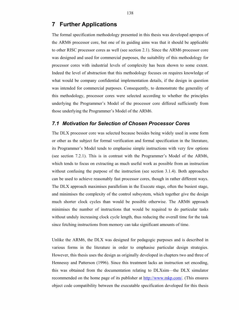
138
7 Further Applications The formal specification methodology presented in this thesis was developed apropos of
the ARM6 processor core, but one of its guiding aims was that it should be applicable
to other RISC processor cores as well (see section 2.1). Since the ARM6 processor core
was designed and used for commercial purposes, the suitability of this methodology for
processor cores with industrial levels of complexity has been shown to some extent.
Indeed the level of abstraction that this methodology focuses on requires knowledge of
what would be company confidential implementation details, if the design in question
was intended for commercial purposes. Consequently, to demonstrate the generality of
this methodology, processor cores were selected according to whether the principles
underlying the Programmer’s Model of the processor core differed sufficiently from
those underlying the Programmer’s Model of the ARM6.
7.1 Motivation for Selection of Chosen Processor Cores
The DLX processor core was selected because besides being widely used in some form
or other as the subject for formal verification and formal specification in the literature,
its Programmer’s Model tends to emphasise simple instructions with very few options
(see section 7.2.1). This is in contrast with the Programmer’s Model of the ARM6,
which tends to focus on extracting as much useful work as possible from an instruction
without confusing the purpose of the instruction (see section 3.1.4). Both approaches
can be used to achieve reasonably fast processor cores, though in rather different ways.
The DLX approach maximises parallelism in the Execute stage, often the busiest stage,
and minimises the complexity of the control subsystem, which together give the design
much shorter clock cycles than would be possible otherwise. The ARM6 approach
minimises the number of instructions that would be required to do particular tasks
without unduly increasing clock cycle length, thus reducing the overall time for the task
since fetching instructions from memory can take significant amounts of time.
Unlike the ARM6, the DLX was designed for pedagogic purposes and is described in
various forms in the literature in order to emphasise particular design strategies.
However, this thesis uses the design as originally developed in chapters two and three of
Hennessy and Patterson (1996). Since this treatment lacks an instruction set encoding,
this was obtained from the documentation relating to DLXsim—the DLX simulator
recommended on the home page of its publisher at http://www.mkp.com/. (This ensures
object code compatibility between the executable specification developed for this thesis
139
and the standard simulator for the DLX.) The control subsystem is also left unspecified,
so this has been extrapolated from one described in Hennessy and Patterson (1994) for
a simplified implementation of the MIPS R2000 processor core (which is developed in
chapters five and six of this book), because the two processor cores are fairly similar.
Despite the above, the DLX processor core used in this thesis is still incomplete in that
the memory model implicit in its memory interface is not very realistic and it provides
no means of raising or handling exceptions. Other designs described in the literature
have resolved these problems in various ways, but no particular solution is standard.
Therefore in order to demonstrate the generality of the methodology of this thesis on
another complete processor, a simplified MIPS R2000 processor core is also used
(inspired in part by the one detailed in Hennessy and Patterson 1994, but not the same).
This forestalls making any arbitrary changes to the original DLX processor core design,
but without necessitating too much extra work given the similarities between the two.
7.2 Overview of the DLX
The DLX processor core supports 32-bit address spaces. It uses a 30-bit address bus for
instruction addresses as all opcodes are 32 bits (one word) in size and must be aligned.
Since it supports byte, halfword (16-bit) and word data transfers, a 32-bit address bus
is used for data accesses. All the data buses (one each for instruction reads, data reads
and data writes) are 32-bit.
Note the DLX presented in Hennessy and Patterson (1996) has an integrated FPU
(Floating-Point Unit), but no implementation details are given on the interaction
between the FPU and the DLX processor core itself. Since the formal specification
developed for the DLX processor core in this thesis therefore does not model the FPU,
the floating-point instructions as well as the multiplication and the division instructions
(which also require the FPU) of the DLX are not considered in this thesis.
7.2.1 Outline of Informal Programmer’s Model Specification
The DLX processor core has one operating mode and supports no exceptions. It has
one register bank of thirty-one general-purpose 32-bit registers numbered R1 – R31;
R0 reads as zero and cannot be altered. The program counter is not directly accessible,
but the return address for subroutines is stored in R31 by the hardware.
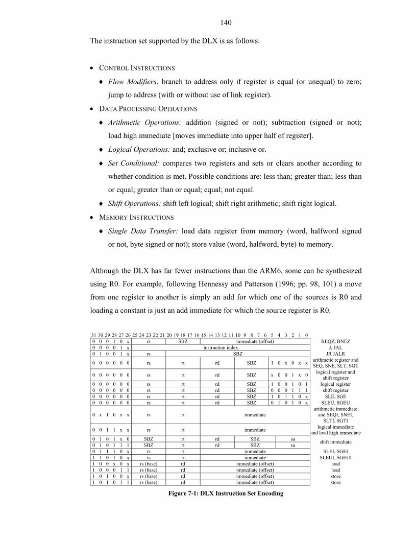
140
The instruction set supported by the DLX is as follows:
• CONTROL INSTRUCTIONS
♦ Flow Modifiers: branch to address only if register is equal (or unequal) to zero;
jump to address (with or without use of link register).
• DATA PROCESSING OPERATIONS
♦ Arithmetic Operations: addition (signed or not); subtraction (signed or not);
load high immediate [moves immediate into upper half of register].
♦ Logical Operations: and; exclusive or; inclusive or.
♦ Set Conditional: compares two registers and sets or clears another according to
whether condition is met. Possible conditions are: less than; greater than; less than
or equal; greater than or equal; equal; not equal.
♦ Shift Operations: shift left logical; shift right arithmetic; shift right logical.
• MEMORY INSTRUCTIONS
♦ Single Data Transfer: load data register from memory (word, halfword signed
or not, byte signed or not); store value (word, halfword, byte) to memory.
Although the DLX has far fewer instructions than the ARM6, some can be synthesized
using R0. For example, following Hennessy and Patterson (1996; pp. 98, 101) a move
from one register to another is simply an add for which one of the sources is R0 and
loading a constant is just an add immediate for which the source register is R0.
31 30 29 28 27 26 25 24 23 22 21 20 19 18 17 16 15 14 13 12 11 10 9 8 7 6 5 4 3 2 1 0 0 0 0 1 0 x rs SBZ immediate (offset) BEQZ, BNEZ 0 0 0 0 1 x instruction index J, JAL 0 1 0 0 1 x rs SBZ JR JALR
0 0 0 0 0 0 rs rt rd SBZ 1 0 x 0 x x arithmetic register andSEQ, SNE, SLT, SGT
0 0 0 0 0 0 rs rt rd SBZ x 0 0 1 x 0 logical register and shift register
0 0 0 0 0 0 rs rt rd SBZ 1 0 0 1 0 1 logical register 0 0 0 0 0 0 rs rt rd SBZ 0 0 0 1 1 1 shift register 0 0 0 0 0 0 rs rt rd SBZ 1 0 1 1 0 x SLE, SGE 0 0 0 0 0 0 rs rt rd SBZ 0 1 0 1 0 x SLEU, SGEU
0 x 1 0 x x rs rt immediate arithmetic immediate
and SEQI, SNEI, SLTI, SGTI
0 0 1 1 x x rs rt immediate logical immediate and load high immediate
0 1 0 1 x 0 SBZ rt rd SBZ sa 0 1 0 1 1 1 SBZ rt rd SBZ sa shift immediate
0 1 1 1 0 x rs rt immediate SLEI, SGEI 1 1 0 1 0 x rs rt immediate SLEUI, SGEUI 1 0 0 x 0 x rs (base) rd immediate (offset) load 1 0 0 0 1 1 rs (base) rd immediate (offset) load 1 0 1 0 0 x rs (base) rd immediate (offset) store 1 0 1 0 1 1 rs (base) rd immediate (offset) store
Figure 7-1: DLX Instruction Set Encoding
141
The following list explains the abbreviations used in Figure 7-1:
• ‘SBZ’ stands for Should Be Zero.
• ‘sa’ stands for shift amount.
• ‘rd’ is the destination register.
• ‘rs’ is the primary source register. (Note if load high immediate then ‘rs’ SBZ.)
• ‘rt’ is the secondary source register or destination register for immediate instructions.
• ‘SEQ’, ‘SNE’, ‘SLT’, ‘SGT’, ‘SLE’, ‘SGE’, ‘SLEU’, ‘SGEU’, ‘SLEI’, ‘SGTI’,
‘SLEUI’ and ‘SGEUI’ are the mnemonics for set conditional instructions.
• ‘BEQZ’ and ‘BNEZ’ are the mnemonics for branch instructions.
• ‘J’, ‘JAL’, ‘JR’ and ‘JALR’ are the mnemonics for jump instructions.
7.2.2 Outline of Informal Hardware Implementation Specification
The DLX processor core memory interface conforms to the Harvard architecture by
having one read port for connection to an instruction memory and one read-write port
for connection to a data memory.
7.2.2.1 Signal Description
Since Hennessy and Patterson (1996) do not detail the input and the output signals that
form the environment of the DLX processor core, only signals for the memory interface
are considered in this thesis. To make comparison with the ARM6 processor core easier,
the signals used approximate those of the modernised ARM6 (see section 5.3.1).
The DLX processor core uses the 32-bit bus DA to present addresses to data memory
and the 30-bit bus IA to present addresses to instruction memory. The data memory
uses the DIN bus to present data to the DLX, which uses the DOUT bus to present data
to data memory; instruction memory uses the IDIN bus to present opcodes to the DLX.
Transfer type is indicated by DMREQ for data memory accesses and IMREQ for
instruction memory accesses: if HIGH in either case then an access is requested
otherwise no access should take place.
Note that the DLX processor core asserts addressing signals in the same clock cycle as
the associated memory access. DMREQ and IMREQ are asserted in φ2 to indicate
whether the relevant memory should drive the pertinent data bus. However, DA and IA
are asserted in φ1 to give the relevant memory time to prepare the memory access.
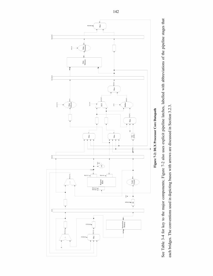
142
Figu
re 7
-2: D
LX
Pro
cess
or C
ore
Dat
apat
h
See
Tabl
e 3-
4 fo
r ke
y to
the
maj
or c
ompo
nent
s; F
igur
e 7-
2 al
so u
ses
expl
icit
pipe
line
latc
hes,
labe
lled
with
abb
revi
atio
ns o
f th
e pi
pelin
e st
ages
that
each
brid
ges.
The
conv
entio
ns u
sed
in d
epic
ting
buse
s with
arr
ows a
re d
iscu
ssed
in S
ectio
n 3.
2.3.
+
IF/ID
Reg
iste
rBa
nk
ID/E
XE
ALU
EXE/
MEM
MEM
/WB
Mux
Mux
Mux
Dat
aM
emor
yD
IN
Instr
uctio
nM
emor
y
ALU
CTL
4
IR[25:21] IR[20:16]
RWEN[0]RWA[3:0]
RS
RT
IDEC
Fiel
dEx
tend
+
IDIN
PCSRC[0]
=0
IDEC
A B
Dat
aSe
lect
orD
OU
T
DA
Dat
aEx
tract
or
MuxREGSRC[0]
DIN
’
DO
UT
PCWEN[0]
BTA
[31:
2]
INC
[31:
2]
PC[3
1:2]
IA[3
1:2]
Shift
er
Mux
SA [4:0
]
Mux
SHO
UT
RES
ULT
SCTL
IMM
[4:0
]
ALU
OU
T
DO
UTC
TL
DIN
CTL
SA’[
4:0]
16
RS[31:]
RD
IMM
IRIRWRITE[0]
143
The following signals are also involved in data memory accesses:
• DnRW (Data not Read, Write): This output is LOW to indicate read transfers
and HIGH to indicate write transfers.
• DSIZE (Data SIZE): This output is ‘00’ to indicate a byte transfer,
‘01’ to indicate a halfword transfer and ‘10’ to indicate a word transfer.
Note since the DLX processor core considered in this thesis does not support exceptions
(see section 7.1), the memory system cannot indicate whether an access failed by
driving an ABORT signal, so it is assumed that memory accesses always succeed.
The following signal reflects the general environment of the DLX processor core:
• nRESET (not RESET): This input is taken LOW to indicate that
the processor core should invalidate the instructions in its pipeline and start fetching
from address 0x00000000.
7.2.2.2 Datapath of Processor Core
The design of the DLX processor core datapath used in this thesis may be depicted as
shown in Figure 7-2.
7.2.2.3 Control Subsystem of Processor Core
The activities performed by the DLX processor core divide into five pipelined stages:
1. INSTRUCTION FETCH: presents signals to instruction memory, if appropriate, to fetch
an instruction and latches the instruction, if any, fetched from instruction memory
in reply to these signals.
2. INSTRUCTION DECODE: decodes the instruction for execution in the next clock cycle
and reads any relevant registers.
3. EXECUTE: performs appropriate calculations.
4. MEMORY: if appropriate, presents signals to data memory to perform an access and
then performs access.
5. WRITEBACK: if appropriate, writes the results to pertinent register.
144
Note that because the DLX processor core does not support instructions that require
multiple clock cycles in the Execute stage, fetch activities occur every clock cycle.
Furthermore, the latches that buffer instructions after fetching, until the Execute stage,
do not need to be considered separately from the pipeline latches that are used to buffer
general signals between pipeline stages. This contrasts with the ARM6 processor core
(see section 3.2.4 and section 5.3.4).
An implementation of the control subsystem of the DLX processor core would require
fewer blocks than the ARM6 processor core, as the following outline shows. (For ease
of comparison, the names used in section 3.2.4 for the ARM6 blocks are also used here
as appropriate.)
• Primary Decode:
♦ IDEC: generates the signals that the Secondary Decode blocks (see below) use
to generate the signals that control the datapath. These signals are generated for
the opcode stored in the IR latch.
• Secondary Decode
♦ ALUCTL: generates the signals that control the ALU.
♦ DCTLBW: generates the DSIZE signal, the signal that controls the data selector
and the signal that controls the data extractor.
♦ SCTL: generates the signals that control the shifter.
♦ SKP: generates the signal that controls the PC multiplexer and the signal that
controls whether the register bank write port is active.
No ‘Instruction Pipeline’ group of control blocks is required, since the pipeline itself
need not be considered apart from the pipeline latches on the datapath, as noted above,
and no state needs to be associated with the instructions in the pipeline. This is because
instruction fetches never abort (see section 7.2.2.1) and branch or jump instructions alter
the program counter in the Instruction Decode stage without invalidating the instruction
resulting from the Fetch stage. The fetched instruction is said to be in the ‘delay slot’ of
the branch or the jump instruction and the compiler, not the hardware, is responsible for
ensuring that it causes no side effects whether the branch is taken or not. If the compiler
inserts a NOP in the delay slot, then the hardware effectively performs a pipeline flush;
but the delay slot may be used more productively as follows:
145
• To insert an instruction that would otherwise precede the branch instruction,
provided this rearrangement does not corrupt the intended algorithm.
• To insert the instruction that would otherwise be the target of the branch instruction,
provided this rearrangement causes no side effects if the branch is not taken.
• To insert an instruction that would otherwise succeed the branch instruction,
provided this rearrangement causes no side effects if the branch is taken.
It is still worthwhile to break the decoding of an instruction into Primary Decode and
Secondary Decode. However Primary Decode only requires an equivalent of IDEC
since neither exceptions nor instructions that need multiple cycles in the Execute stage
are supported by the DLX processor core. Secondary Decode also requires fewer blocks
because the regularity of the encoding of source registers and the destination register
means that the signals that would otherwise need to be produced by equivalents of
ACTL, BCTL and WCTL can be generated by IDEC directly. Regularity of encoding
also allows direction generation of the signal that controls how an immediate is formed
by IDEC. Nonetheless, encoding also complicates some aspects of Secondary Decode.
For example, bits 31 – 26 determine the function of data processing instructions that
do not use an immediate and bits 5 – 0 the function of those that do, but the encoding of
these bits is sufficiently irregular to require ALUCTL to treat each separately.
Data Hazard An instruction in the Execute stage at tn and the Memory stage at tn + 1,
will not write any result of calculations in the former or any result of
reading memory in the latter into its destination register until tn + 2.
Hence if the instructions that are in the Execute stage at tn + 1 or tn + 2
need either of these results, the relevant register cannot be read as usual
in the corresponding Instruction Decode stage (tn or tn + 1).
Resolution In general, forwarding logic is used so that, irrespective of the value
read at tn or tn + 1 the A or B multiplexers can select the correct value
at tn + 1 and tn + 2. However, values read from memory are not available
until tn + 2 so that an instruction which requires the memory value at tn + 1
must be interlocked in the Instruction Decode stage for one clock cycle.
Store instructions bypass the forwarding logic to obtain the value of
the register to store (the B multiplexer must pass on the immediate value
so that the address can be calculated) and thus must be interlocked in
the Instruction Decode stage for two clock cycles in the worst cases.
146
Data Hazard The value of the relevant source register of branch instructions and
jump instructions is used in the same Instruction Decode stage it is read.
Hence changes that would be made to this register when the instructions
in the Execute stage and in the Memory stage enter the Writeback stage
would be disregarded.
Resolution Forwarding cannot be used so the branch instruction or jump instruction
must interlock in the Instruction Decode stage for two clock cycles or
one clock cycle, depending on whether the instruction that would alter
the source register is in the Execute stage or the Memory stage.
Table 7-1: Data Hazards of DLX
The DLX processor core has neither structural hazards (due to the relative simplicity of
its instruction set) nor control hazards (since these are exposed by its use of delay slots
to the Programmer’s Model) unlike the modernised ARM6 (see section 5.3.4).
Nevertheless it does possess a number of Read After Write data hazards, as summarised
in Table 7-1.
7.3 Specifying the DLX
The specification of the DLX processor core developed for this thesis (see Appendix A
for the mathematical presentation and Appendix B for the engineering presentation;
no executable presentation was developed) defines the following instruction classes:
• CONTROL INSTRUCTIONS
♦ ctrl: encapsulates flow modifiers (see section 7.2.1).
• DATA PROCESSING OPERATIONS
♦ data: encapsulates arithmetic operations, logical operations, set conditional and
shift operations (see section 7.2.1).
• MEMORY INSTRUCTIONS
♦ load: encapsulates single data transfers from memory to the DLX processor core
(see section 7.2.1).
♦ store: encapsulates single data transfers from the DLX processor core to memory
(see section 7.2.1).
147
• NULL INSTRUCTIONS
♦ stall: inserted in the Instruction Decode stage by pipeline control logic to interlock
the instruction class associated with the opcode latched in IR.
♦ undef: used when an opcode cannot be decoded into one of the instructions
defined by the Programmer’s Model specification for the DLX processor core
(see section 7.2.1).
The formal specification of the DLX processor core did not require any further changes
to the methodology of this thesis following those made for the formal specification of
the modernised ARM6 (see section 6). Nonetheless the application of this methodology
to the DLX processor core did give rise to some interesting observations:
1. On the DLX processor core, branch instructions and jump instructions are optimised
to modify the program counter in the Instruction Decode stage so that the compiler
does not need to manage more than one branch delay slot. (The compiler is unlikely
to be able to use any additional branch delay slots as productively as it can the first.)
Hence, specification of the instruction fetch pipeline activity must be split between
the Instruction Decode stage and the Execute stage, in contrast to its specification for
the original ARM6 and the modernised ARM6 as part of the Execute stage only.
Although this split could be made by the specification of just the transfer that updates
the program counter in the Instruction Decode stage, this would be rather inelegant;
thus φ1 of the instruction fetch pipeline activity is specified in the Execute stage,
whereas φ2 is specified in the Instruction Decode stage. (To split the specification of
a pipeline activity between two or more pipeline stages is not problematic as long as
it is clear that this does not introduce any conflicts between the transfers required by
the pipeline activity.) Furthermore, to stall the pipeline on the DLX processor core
the stall instruction class itself must be inserted in the Instruction Decode stage,
whereas on the modernised ARM6 processor core it is inserted in the Execute stage.
(In both cases the instruction class that requires the stall, because it cannot proceed to
the Execute stage, is interlocked in the Instruction Decode stage, but in the latter case
it still dictates the pipeline activities for this pipeline stage.)
2. The need for some form of pipeline flushing mechanism on the DLX processor core
is avoided by the use of a delay slot for branch instructions and jump instructions.
This simplifies the control logic required to implement the DLX and in turn
simplifies the formal specification of an implementation of the DLX.
148
3. As the DLX processor core lacks any instructions that require multiple clock cycles
in the Execute stage, no distinction between instruction steps and instruction classes
needs to be made in its formal specification.
4. The dataflow for data processing instructions that perform shifts rather than
arithmetic or logic, is quite different on the DLX processor core. Hence instead of
using one instruction class for data processing instructions with appropriate options,
two instruction classes could have been used. This would permit the identification,
for each instruction class, of one function to specify solely its distinctive behaviour;
other functions would just specify default behaviours. Yet while this would reflect
the differences in emphasis between the Programmer’s Model of the DLX and that of
the ARM6 (see section 7) most clearly, one instruction class was used to highlight
similarity of usage for all data processing instructions. (Moreover this allows some of
the more advanced techniques of the methodology of this thesis to be exemplified.)
7.4 Overview of the Simplified MIPS R2000
The MIPS R2000 processor core uses one 32-bit address bus and one 32-bit data bus for
accessing 32-bit address spaces. Although it does not use separate buses to perform
instruction accesses and data accesses, the buses are used in alternate clock phases for
instruction accesses and data accesses, so both types of accesses may be performed in
one clock cycle. It supports byte, halfword (16-bit) and word data transfers as well as
word instruction transfers.
The MIPS R2000 discussed in this thesis is based on the simplified version presented in
Hennessy and Patterson (1994), but with various alterations to make it more similar to
the commercial version detailed in the standard reference of Kane and Heinrich (1992).
7.4.1 Outline of Informal Programmer’s Model Specification
The commercial version of the MIPS R2000 processor core has two operating modes
and supports various exceptions. Up to four coprocessors may be attached to it.
However, the version of the MIPS R2000 presented in this thesis supports a subset of
the exceptions supported by the commercial version and has only one operating mode.
Although it does not support coprocessors, it implements two registers extracted from
the system control coprocessor that relate to exception handling.

149
The register bank organization of the MIPS R2000 is identical to that of the DLX: it has
one register bank of thirty-one general-purpose 32-bit registers numbered R1 – R31;
R0 reads as zero and cannot be altered. The program counter is not directly accessible,
but by default the return address for subroutines is stored in R31 by the hardware.
The instruction set supported by the MIPS R2000 processor core presented in this thesis
and by the commercial version is identical except for coprocessor instructions:
• CONTROL INSTRUCTIONS
♦ Flow Modifiers: branch to address only if condition is passed (and some, with or
without use of link register); jump to address (with or without use of link register);
jump to register (with or without use of specified register as link register).
♦ Mode Modifiers: system call [allows user code to call operating system code];
breakpoint trap [allows user code to call debugging code].
• DATA PROCESSING OPERATIONS
♦ Arithmetic Operations: addition (signed or not); subtraction (signed or not);
load upper immediate [moves immediate into upper half of register].
♦ Logical Operations: and; exclusive or; inclusive or; not or.
♦ Set Conditional: compares register with value and sets or clears another register
according to whether it is less than (signed or not) that value.
♦ Shift Operations: shift left logical; shift right arithmetic; shift right logical.
• MEMORY INSTRUCTIONS
♦ Single Data Transfer: load data register from memory (non-aligned word, word,
halfword signed or not, byte signed or not); store value (non-aligned word, word,
halfword, byte) to memory.
• COPROCESSOR INSTRUCTIONS
♦ Move From Coprocessor: load data register from coprocessor register
[implemented only to access registers extracted from system control coprocessor].
• INSTRUCTION SET EXTENDERS
♦ Reserved Instruction: cause a reserved instruction exception.
Note the main difference between signed operations and unsigned operations is that
overflow exceptions (see below) may be raised with the former but not with the latter.
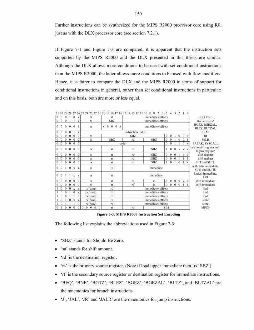
150
Further instructions can be synthesized for the MIPS R2000 processor core using R0,
just as with the DLX processor core (see section 7.2.1).
If Figure 7-1 and Figure 7-3 are compared, it is apparent that the instruction sets
supported by the MIPS R2000 and the DLX presented in this thesis are similar.
Although the DLX allows more conditions to be used with set conditional instructions
than the MIPS R2000, the latter allows more conditions to be used with flow modifiers.
Hence, it is fairer to compare the DLX and the MIPS R2000 in terms of support for
conditional instructions in general, rather than set conditional instructions in particular;
and on this basis, both are more or less equal.
31 30 29 28 27 26 25 24 23 22 21 20 19 18 17 16 15 14 13 12 11 10 9 8 7 6 5 4 3 2 1 0 0 0 0 1 0 x rs rt immediate (offset) BEQ, BNE 0 0 0 1 1 x rs SBZ immediate (offset) BGTZ, BLEZ
0 0 0 0 0 1 rs x 0 0 0 x immediate (offset) BGEZ, BGEZAL, BLTZ, BLTZAL
0 0 0 0 1 x instruction index J, JAL 0 0 0 0 0 0 rs SBZ 0 0 1 0 0 0 JR 0 0 0 0 0 0 rs SBZ rd SBZ 0 0 1 0 0 1 JALR 0 0 0 0 0 0 code 0 0 1 1 0 x BREAK, SYSCALL
0 0 0 0 0 0 rs rt rd SBZ 1 0 0 x x x arithmetic register andlogical register
0 0 0 0 0 0 rs rt rd SBZ 0 0 0 1 x 0 shift register 0 0 0 0 0 0 rs rt rd SBZ 0 0 0 1 1 1 shift register 0 0 0 0 0 0 rs rt rd SBZ 1 0 1 0 1 x SLT and SLTU
0 0 1 0 x x rs rd immediate arithmetic immediate,SLTI and SLTIU
0 0 1 1 x x rs rt immediate logical immediate, LUI
0 0 0 0 0 0 rs rt rd sa 0 0 0 0 x 0 shift immediate 0 0 0 0 0 0 rs rt rd sa 0 0 0 0 1 1 shift immediate 1 0 0 0 x x rs (base) rd immediate (offset) load 1 0 0 1 0 x rs (base) rd immediate (offset) load 1 0 0 1 1 0 rs (base) rd immediate (offset) load 1 0 1 0 x x rs (base) rd immediate (offset) store 1 0 1 1 1 0 rs (base) rd immediate (offset) store 0 1 0 0 0 0 0 0 0 0 0 rt rd SBZ MFC0
Figure 7-3: MIPS R2000 Instruction Set Encoding
The following list explains the abbreviations used in Figure 7-3:
• ‘SBZ’ stands for Should Be Zero.
• ‘sa’ stands for shift amount.
• ‘rd’ is the destination register.
• ‘rs’ is the primary source register. (Note if load upper immediate then ‘rs’ SBZ.)
• ‘rt’ is the secondary source register or destination register for immediate instructions.
• ‘BEQ’, ‘BNE’, ‘BGTZ’, ‘BLEZ’, ‘BGEZ’, ‘BGEZAL’, ‘BLTZ’, and ‘BLTZAL’ are
the mnemonics for branch instructions.
• ‘J’, ‘JAL’, ‘JR’ and ‘JALR’ are the mnemonics for jump instructions.
151
• ‘code’ is ignored by the hardware and may be used for software parameters.
• ‘BREAK’, ‘SYSCALL’ are the mnemonics for mode modifiers.
• ‘SLT’, ‘SLTU’, ‘SLTI’, ‘SLTUI’, are the mnemonics for set conditional instructions.
• ‘MFC0’ is the mnemonic for move from coprocessor instruction.
The following eight exceptions may be raised on the MIPS R2000 processor core
presented in this thesis:
1. RESET: occurs when the nRESET input to the processor core is deasserted after being
taken LOW and is used to initialise the MIPS R2000 when first powered up.
2. INSTRUCTION ADDRESS: occurs when a non-aligned instruction access is attempted
(this can only happen because of jump register instructions).
3. INTEGER OVERFLOW: occurs when ALU performs signed operation that resulted in
2’s-complement overflow.
4. SYSTEM CALL: occurs when the processor core executes the SYSCALL instruction.
5. BREAKPOINT TRAP: occurs when the processor core executes the BREAK instruction.
6. RESERVED INSTRUCTION: occurs when the processor core attempts to execute
instructions not defined in Figure 7-3.
7. LOAD ADDRESS: occurs when a non-aligned data load is attempted, except when
instruction explicitly allows non-aligned data access (that is: LWL or LWR).
8. STORE ADDRESS: occurs when a non-aligned data store is attempted, except when
instruction explicitly allows non-aligned data access (that is: SWL or SWR).
Reset is distinguished from other exceptions by the use of 0xbfc00000 as the address
from which instruction pre-fetching is started; the other exceptions use 0xbfc00100.
Therefore all exceptions except for reset must write the appropriate exception code into
the cause register (register 13 in the system control coprocessor):
2. INSTRUCTION ADDRESS = 4
3. INTEGER OVERFLOW = 12
4. SYSTEM CALL = 8
5. BREAKPOINT TRAP = 9
6. RESERVED INSTRUCTION = 10
7. LOAD ADDRESS = 4
8. STORE ADDRESS = 5
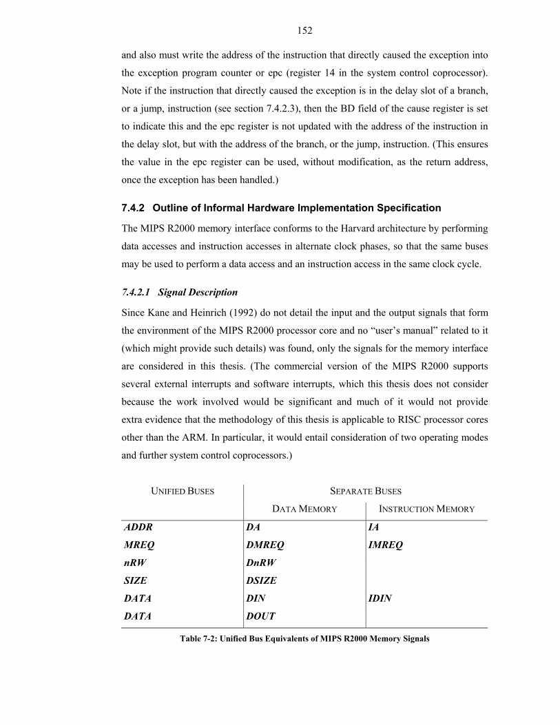
152
and also must write the address of the instruction that directly caused the exception into
the exception program counter or epc (register 14 in the system control coprocessor).
Note if the instruction that directly caused the exception is in the delay slot of a branch,
or a jump, instruction (see section 7.4.2.3), then the BD field of the cause register is set
to indicate this and the epc register is not updated with the address of the instruction in
the delay slot, but with the address of the branch, or the jump, instruction. (This ensures
the value in the epc register can be used, without modification, as the return address,
once the exception has been handled.)
7.4.2 Outline of Informal Hardware Implementation Specification
The MIPS R2000 memory interface conforms to the Harvard architecture by performing
data accesses and instruction accesses in alternate clock phases, so that the same buses
may be used to perform a data access and an instruction access in the same clock cycle.
7.4.2.1 Signal Description
Since Kane and Heinrich (1992) do not detail the input and the output signals that form
the environment of the MIPS R2000 processor core and no “user’s manual” related to it
(which might provide such details) was found, only the signals for the memory interface
are considered in this thesis. (The commercial version of the MIPS R2000 supports
several external interrupts and software interrupts, which this thesis does not consider
because the work involved would be significant and much of it would not provide
extra evidence that the methodology of this thesis is applicable to RISC processor cores
other than the ARM. In particular, it would entail consideration of two operating modes
and further system control coprocessors.)
UNIFIED BUSES SEPARATE BUSES
DATA MEMORY INSTRUCTION MEMORY
ADDR DA IA
MREQ DMREQ IMREQ
nRW DnRW
SIZE DSIZE
DATA DIN IDIN
DATA DOUT
Table 7-2: Unified Bus Equivalents of MIPS R2000 Memory Signals
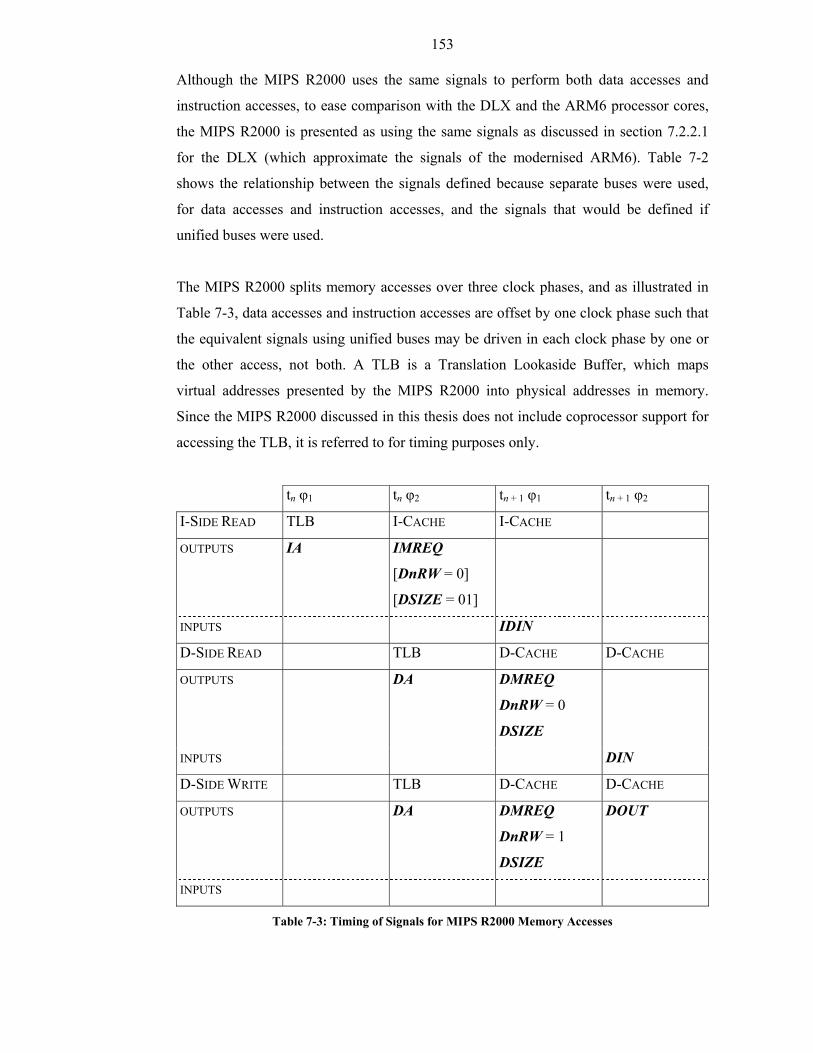
153
Although the MIPS R2000 uses the same signals to perform both data accesses and
instruction accesses, to ease comparison with the DLX and the ARM6 processor cores,
the MIPS R2000 is presented as using the same signals as discussed in section 7.2.2.1
for the DLX (which approximate the signals of the modernised ARM6). Table 7-2
shows the relationship between the signals defined because separate buses were used,
for data accesses and instruction accesses, and the signals that would be defined if
unified buses were used.
The MIPS R2000 splits memory accesses over three clock phases, and as illustrated in
Table 7-3, data accesses and instruction accesses are offset by one clock phase such that
the equivalent signals using unified buses may be driven in each clock phase by one or
the other access, not both. A TLB is a Translation Lookaside Buffer, which maps
virtual addresses presented by the MIPS R2000 into physical addresses in memory.
Since the MIPS R2000 discussed in this thesis does not include coprocessor support for
accessing the TLB, it is referred to for timing purposes only.
tn φ1 tn φ2 tn + 1 φ1 tn + 1 φ2
I-SIDE READ TLB I-CACHE I-CACHE
OUTPUTS IA IMREQ
[DnRW = 0]
[DSIZE = 01]
INPUTS IDIN
D-SIDE READ TLB D-CACHE D-CACHE
OUTPUTS DA DMREQ
DnRW = 0
DSIZE
INPUTS DIN
D-SIDE WRITE TLB D-CACHE D-CACHE
OUTPUTS DA DMREQ
DnRW = 1
DSIZE
DOUT
INPUTS
Table 7-3: Timing of Signals for MIPS R2000 Memory Accesses
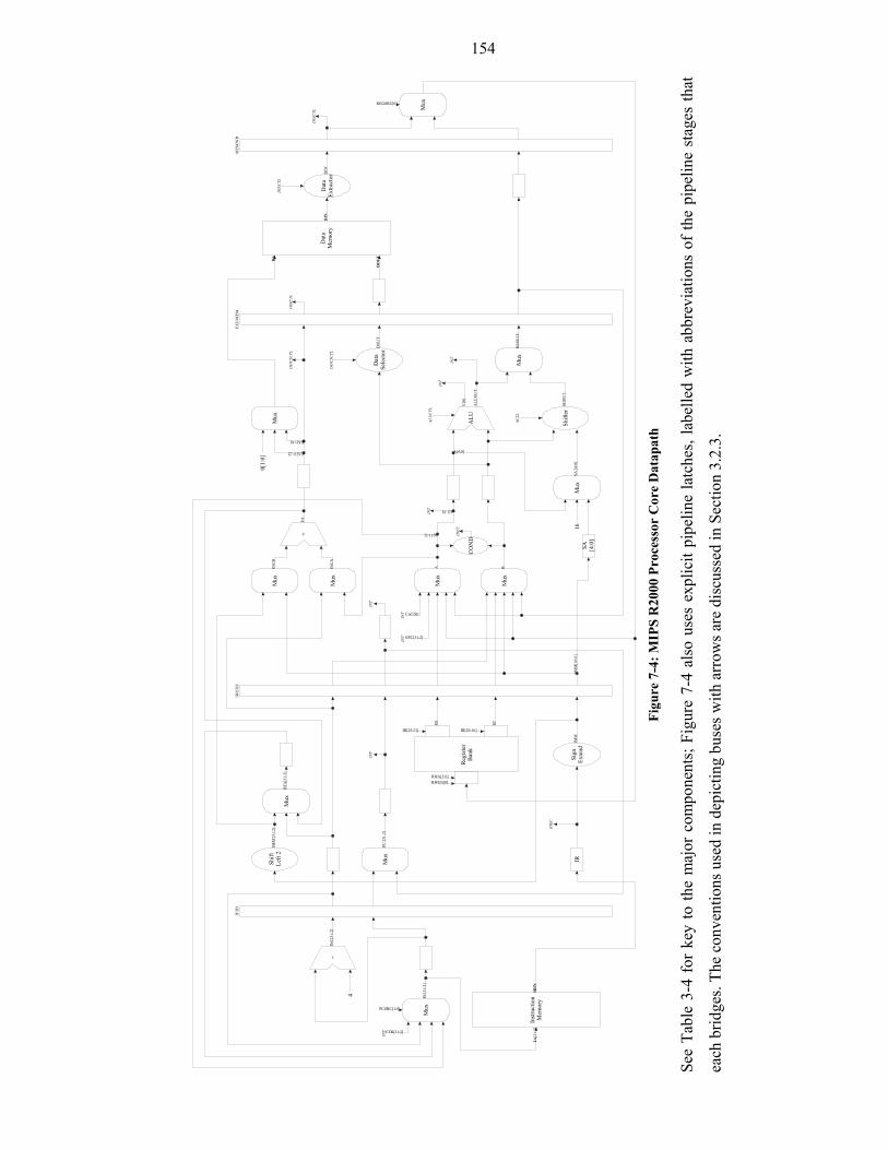
154
Figu
re 7
-4: M
IPS
R20
00 P
roce
ssor
Cor
e D
atap
ath
See
Tabl
e 3-
4 fo
r ke
y to
the
maj
or c
ompo
nent
s; F
igur
e 7-
4 al
so u
ses
expl
icit
pipe
line
latc
hes,
labe
lled
with
abb
revi
atio
ns o
f th
e pi
pelin
e st
ages
that
each
brid
ges.
The
conv
entio
ns u
sed
in d
epic
ting
buse
s with
arr
ows a
re d
iscu
ssed
in S
ectio
n 3.
2.3.
+
IF/ID
Regi
ster
Ban
k
ID/E
XE
ALU
EXE/
MEM
MEM
/WB
Mux
Mux
Mux
Dat
aM
emor
yD
IN
Instr
uctio
nM
emor
y
ALU
CTL
4
IR[25:21] IR[20:16]
RWEN[0]RWA[3:0]
RS
RT
IDEC
Sign
Exte
nd
Shift
Left
2
+
PCSRC[1:0]
CON
D
IDEC
V[0
]
INT
Dat
aSe
lect
orD
OU
T
Dat
aEx
tract
or
MuxREGSRC[0]
DIN
’
DO
UT
IR
Mux
Mux
Mux
Shift
er
Mux
SA [4:0
]
IMM
[10:
6]IM
M
BA
A[4:0]
Mux
SHO
UT
RES
ULT
SCTL
INT
ALU
OU
T
EPC[31:2]
INT
VTR[31:2]
INT
INC
[31:
2]
IA[3
1:2]
A[31:2]
A[1:0]
INT
BTA
[31:
2]
DA
IMM
’[31
:2]
DO
UTC
TL
DIN
CTL
SA’[
4:0]
16
INC
A
INC
B
EA
DIN
CTL
DO
UTC
TL
Mux
0[1:
0]
DIN
CTL
Mux
PC’[
31:2
]
PC[3
1:2]
IDIN
INT CAUSE
INT
INT
EA[1:0]
EA[31:2]
155
The MIPS R2000 detects address exceptions (see section 7.4.1) by itself, thus to allow
the memory system to indicate that an access failed by driving an ABORT signal,
would introduce unnecessary complications, without providing much more evidence of
the applicability of the methodology of this thesis to RISC processor cores other than
the ARM.
The following signal reflects the general environment of the DLX processor core:
• nRESET (not RESET): This input is taken LOW to indicate that
the processor core should invalidate the instructions in its pipeline and start fetching
from address 0xbfc00000.
7.4.2.2 Datapath of Processor Core
The design of the datapath of the MIPS R2000 processor core presented in this thesis
may be depicted as shown in Figure 7-4. Note the EA adder may be used to calculate
data addresses in φ1 and instruction addresses in φ2, thus preventing the necessity for
two separate adders.
7.4.2.3 Control Subsystem of Processor Core
The activities performed by the MIPS R2000 divide into five pipelined stages:
1. INSTRUCTION FETCH: presents signals to instruction memory, if appropriate, to fetch
an instruction.
2. INSTRUCTION DECODE: latches instruction, if any, fetched from instruction memory
in response to the signals asserted in the Instruction Fetch stage and decodes it for
execution in the next clock cycle; reading any relevant registers.
3. EXECUTE: performs appropriate calculations and, if appropriate, presents address to
data memory to prepare for an access in the Memory stage.
4. MEMORY: if appropriate, presents signals to data memory to perform an access and
then performs access.
5. WRITEBACK: if appropriate, writes the results to pertinent register.
Note that as with the DLX processor core (see section 7.2.2.3), fetch activities occur
every clock cycle.
156
An implementation of the control subsystem of the MIPS R2000 discussed in this thesis
would require fewer blocks than the ARM6, as the following outline shows. (For ease
of comparison, the names used in section 3.2.4 for the ARM6 blocks are also used here
as appropriate.)
• Instruction Pipeline:
♦ PIPESTAT: records whether the opcode latched in the IR latch this clock cycle
should be flushed because an exception was taken in the previous clock cycle.
• Primary Decode:
♦ IDEC: generates the signals that the Secondary Decode blocks (see below) use
to generate the signals that control the datapath. These signals are generated for
the opcode stored in the IR latch.
♦ INT: detects exceptions. This block indicates when to handle exceptions
(recording status information as needed), prioritising if more than one is pending.
It is also responsible for updating the cause and the epc registers.
• Secondary Decode
♦ ALUCTL: generates the signals that control the ALU and the EA adder.
♦ DCTLBW: generates the DSIZE signal, the signal that controls the data selector
and the signal that controls the data extractor.
♦ SCTL: generates the signals that control the shifter.
♦ SKP: generates the signal that controls the PC multiplexer and the signal that
controls whether the register bank write port is active.
This outline is very similar to that for the DLX in section 7.2.2.3; the main difference
being the addition of the PIPESTAT and the INT control blocks for exception handling.
(The comments made for the DLX, in this section, on the use of branch delay slots and
the regularity of instruction encoding apply equally to the MIPS R2000.) In contrast to
the DLX (see Table 7-1), the MIPS R2000 has only one Read After Write data hazard,
as summarised in Table 7-4, and has no requirement for logic to interlock the pipeline
because unlike the DLX it makes:
• use of delay slots for load instructions,
• use of a separate adder, rather than the ALU, to calculate store addresses,
• branch instructions and jump instructions not bypass forwarding paths.
157
Data Hazard An instruction in the Execute stage at tn and the Memory stage at tn + 1,
will not write any result of calculations in the former or any result of
reading memory in the latter into its destination register until tn + 2.
Hence if the instructions that are in the Execute stage at tn + 1 or tn + 2
need either of these results, the relevant register cannot be read as usual
in the corresponding Instruction Decode stage (tn or tn + 1).
Resolution In general, forwarding logic is used so regardless of the value read at tn
or tn + 1 the A, or B multiplexers can select the correct value at tn + 1
and tn + 2. However values read from memory are not available until tn + 2
so an instruction at tn + 1 is said to be in the ‘delay slot’ of a load at tn and
it is the compiler, not the hardware, that is responsible for ensuring that
the instruction at tn + 1 does not require the value read from memory.
(The only exception to this concerns the lwl and the lwr instructions,
since forwarding of the value from the writeback stage to the extractor
is implemented to handle this case.) Although the compiler may insert
a NOP in the delay slot such that the hardware effectively interlocks,
the delay slot may be used more productively by rearranging
instructions around the load instruction to insert one that does not use
the value it reads from memory, provided that the intended algorithm
is not corrupted.
Table 7-4: Data Hazards of MIPS R2000
The MIPS R2000 has no control hazards due to flow modifiers, since these are exposed,
as with the DLX, to the Programmer’s Model by the use of delay slots. However, it has
one control hazard due to how exceptions are handled: the exception instruction class
enters the Execute pipeline stage when the instruction that caused the exception leaves
the pipeline stage in which the exception was detected. Therefore, the instruction that
caused the exception and the instruction that was fetched while the exception occurred
must be flushed.
7.5 Specifying the Simplified MIPS R2000
The following instruction classes were used to specify the MIPS R2000 developed for
this thesis:
• CONTROL INSTRUCTIONS
♦ ctrl: encapsulates flow modifiers (see section 7.4.1).
158
♦ excp: encapsulates mode modifiers and exceptions (see section 7.4.1).
• DATA PROCESSING OPERATIONS
♦ data: encapsulates arithmetic operations, logical operations, set conditional and
shift operations (see section 7.4.1).
• MEMORY INSTRUCTIONS
♦ load: encapsulates single data transfers from memory to the MIPS R2000
(see section 7.4.1).
♦ store: encapsulates single data transfers from the MIPS R2000 to memory
(see section 7.4.1).
• COPROCESSOR INSTRUCTIONS
♦ mfc: encapsulates reading the cause and the epc registers (see section 7.4.1).
• NULL INSTRUCTIONS
♦ unexec: inserted in the Instruction Decode stage by pipeline control logic to flush
the instruction class associated with the opcode latched in IR.
Most of the differences between this list of instruction classes and the list presented for
the DLX in section 7.3 relate to the support the MIPS R2000 provides for exceptions.
Since the DLX discussed in this thesis does not support exceptions, no equivalents for
the excp, the mfc and the unexec instruction classes were defined for the DLX.
Furthermore, no equivalent for the undef instruction class of the DLX was defined for
the MIPS R2000 because the MIPS R2000 uses the excp instruction class to decode
reserved instructions (since if the reserved instruction enters the Execute pipeline stage,
an exception should be raised).
It was not necessary to define an equivalent for the stall instruction class of the DLX,
because the MIPS R2000 does not need to use pipeline interlocks to resolve hazards
(see section 7.2.2.3).
As for the formal specification of the DLX processor core, the formal specification of
the MIPS R2000 processor core did not require further changes to the methodology of
this thesis following those made for the formal specification of the modernised ARM6
(see section 6). Of the observations cited in section 7.3, in relation to the application of
this methodology to the DLX processor core, 3 and 4 are relevant to the application of
this methodology to the MIPS R2000 processor core as well.
159
Only the mathematical presentation of the formal specification of the MIPS R2000
processor core was created, but this was sufficient to make the following observations:
1. The DLX presented in section 7.2 and the MIPS R2000 are sufficiently similar that
the forwarding logic can be specified for both using the same function. Other logic,
and some of the transfers each makes, were sufficiently similar that the specification
for the DLX could be adapted for the MIPS R2000 in each case. This illustrates that
the specifications created with the methodology of this thesis can be used to compare
the features of different designs.
2. Although the value on the PC[31:2] bus is pipelined in case the pipeline control logic
needs to update the epc register because an exception has occurred, it was convenient
to specify the pipelining on the datapath, rather than as part of pipeline control logic.
Not only did this allow the latches involved in the pipelining to be abstracted away
in favour of the pipeline latches that are used to buffer general signals between
pipeline stages, but it clarified the relation between the value selected for PC'[31:2]
and the instruction class in the Execute stage. (The ctrl instruction class forces
selection of the value of PC[31:2] associated with itself and not that associated with
the instruction class in the Instruction Decode stage; see section 7.4.1.)
3. The version of the MIPS R2000 developed for this thesis accurately models much of
the behaviour that would be expected of the commercial version of the MIPS R2000
processor core in relation to memory accesses. In particular, it models the timing of
the signals involved in memory accesses correctly to the level of the clock phase.
Therefore, the successful application of the methodology of this thesis in specifying
the version of the MIPS R2000 presented in this thesis shows that this methodology
is not limited to processor cores that perform memory accesses in the same way as
the ARM6, or in some unrealistic fashion (like the DLX). (The main simplification in
the memory model implemented by the MIPS R2000 presented in this thesis
concerns not providing any means for the memory system to indicate when an access
should not occur. However, the alterations required to eliminate this simplification
would be similar to those made to the specification of the modernised ARM6 to add
support for data aborts, because the simplification was made more to reduce the work
needed to specify pipeline control rather than to reduced the work needed to specify
memory accesses.)
4. Although the exception model of the commercial version of the MIPS R2000
processor core was not completely implemented for the version of the MIPS R2000
160
developed for this thesis, most of its characteristic features were adopted in one form
or another. For example: the use of the cause register instead of exception vectors for
all but the reset exception; the relation between the instruction that was the cause of
the exception and the return address that is stored; as well as that the return address
is stored in a dedicated register (the epc)—not the default link register. Such features
are quite different from the exception model used by both the original ARM6 and
the modernised ARM6, yet no modifications were required to the methodology of
this thesis when the mathematical presentation of a processor core with these features
was created. This provides further evidence of the applicability of this methodology
to RISC processor cores other than the ARM.
7.6 Summary
While no engineering presentation was created for the specification of the MIPS R2000
processor core, no problems were encountered when the methodology outlined in
section 2.3.2 was used to create one for the specification of the DLX processor core.
Likewise, no executable presentations were created for either of these specifications,
but as the development of both specifications was straightforward, at least in terms of
applying the methodology of this thesis to create the mathematical presentations,
creating an executable presentation of either specification should not prove difficult.
Indeed the Standard ML executable presentation developed for the modernised ARM6
implements every feature of the specifications of both the DLX and the MIPS R2000
(like explicit pipeline buffers) that would require alterations in the reusable modules of
its general simulator.
No changes were required to the general methodology of this thesis so it could be used
to create the formal specification of the DLX and the MIPS R2000 processor cores
presented in this thesis. This serves to illustrate the applicability of this methodology
to all RISC processor cores and not just one example.
Only an informal Programmer’s Model specification such as that given in section 7.2.1,
or section 7.4.1, and the datapath schematics of Figure 7-2 and Figure 7-4 were used
to develop the formal specification of the DLX and the MIPS R2000 processor cores—
no Hardware Implementation specification was used. This shows that the methodology
of this thesis can be used for designing processor cores, rather than just for formalising
a particular design after it has been created.
161
8 Conclusions Four different processor cores were specified using the methodology of this thesis for
this thesis. In part this was possible because of the similarities between the DLX and
the MIPS R2000 on the one hand and the original ARM6 and the modernised ARM6 on
the other. Nevertheless, each of these processor cores had particular features that made
the application of the methodology of this thesis worthwhile (see section 4, section 6,
section 7.3 and section 7.5).
The Phase specification of the original ARM6 describes the original ARM6 in terms of
the same entities as the ARM2x Block Specifications (albeit with tristate buffers and
other logic that is not readily synthesizable replaced with equivalent logic that is),
which describe the original ARM6 at the RTL level of abstraction. This illustrates that,
as required by its first aim (see section 2.1), the methodology of this thesis may be used
to create formal specifications that model accurately those aspects of a hardware design
essential to the correct operation of a processor core at the RTL level of abstraction.
Evidence that the methodology of this thesis is applicable to all RISC processor cores,
and thus meets its second aim, is supplied by the mere fact of its successful application
to four different processor cores. Moreover, the development of three presentations—
the mathematical for formal verification, the engineering to minimise the prerequisite
formal methods background and the executable to facilitate automation of simulation—
makes it clear how the methodology of this thesis meets its third and fourth aims.
Consequently, the methodology of this thesis is suitable for the formal specification of
processor cores at the RTL level of abstraction.
The methodology of this thesis might be further developed as follows:
• An algorithm could be created to automate the process of converting between each of
the different presentations, and in particular, from the engineering to the executable.
If all but the initial presentation of the specification of a processor core were created
by the application of this algorithm to the initial presentation, then formal proof of
the correctness of this algorithm would be sufficient to show that each presentation
is identical to the other presentations of the specification of a processor core.
• Although the Phase specifications that may be generated with the methodology of
this thesis and the corresponding Hardware Implementation specifications are of
162
slightly different levels of abstraction (see section 2.2), it is not inconceivable that
an algorithm could be created to generate a Hardware Implementation specification
(particularly if described in Verilog or some other hardware description language)
from a Phase specification. Again, formal proof of the correctness of this algorithm
would be sufficient to demonstrate that the Hardware Implementation specification
and the Phase specification are consistent with each other.
• The transfers, as well as the interpretations of the associated uninterpreted functions,
which constitute the Phase specifications that can be created with the methodology of
this thesis, could be readily translated into the proprietary property languages of
commercial model checking tools. The relevant tool could then be used to check
equivalence of the formal specification created using the methodology of this thesis
and an existing synthesisable RTL Hardware Implementation specification.
• Although only latch based designs that required clock cycles of two distinct phases
were considered in this thesis, the methodology of this thesis can be easily adapted to
flip-flop based designs that operate on the positive or the negative edge of a clock
by considering only one distinct phase. (In which case, the mechanism described for
the simulation of updates to sequential logic in section 2.3.3 behaves similarly to
the non-blocking assignment of Verilog.)
• Processor cores with complex microarchitectures comprised of several components,
such as separate units to perform memory fetches independently of the main unit that
performs the integer operations, are becoming more frequent. The methodology of
this thesis could be adapted for such processor cores by stipulating each component
requires separate specification in the same way that the datapath, the datapath control
and the pipeline control do. It is likely that other changes would be necessary also,
because such processor cores are quite different from those specified for this thesis.
163
Bibliography Anderson, Allan H. and Shaw, Gary A. (1997) “Executable Requirements and
Specifications” in Journal of VLSI Signal Processing, Vol. 15, pp. 49-61.
ARM (1991) ARM6 Design Documentation.
ARM (1991) ARM2x Block Specifications.
ARM (1993) ARM DDI0001F: ARM6 Data Sheet.
ARM (1996) ARM DDI0004E: ARM610 Data Sheet.
Bergeron, Janick (2000) Writing Testbenches: Functional Verification of HDL Models.
Kluwer Academic Publishers.
Bickford, M. (2000) “Verifying a Pipelined Microprocessor” in The 19th Digital
Avionics Systems Conference, Vol. 1, pp. 1A5/1-1A5/8.
Blumenröhr, C. and Eisenbiegler, D. (1997) “An Efficient Representation for Formal
Synthesis” in 10th Tenth International Symposium on System Synthesis, pp. 9-15.
Burch, J. R. and Dill, D. L. (1994) “Automatic verification of pipelined microprocessor
control” in Computer-Aided Verification, Vol. 818 of Lecture Notes in Computer
Science, Springer-Verlag, pp. 68-80.
Chander, Subash and Vaideeswaran (2001) “Addressing Verification Bottlenecks of
Fully Synthesized Processor Cores using Equivalence Checkers” in Proceedings of
ASP-DAC 2001, pp. 175-180.
Coe, Michael (1994). Results from Verifying a Microprocessor. Master Thesis,
Laboratory for Applied Logic, University of Idaho at ftp://lal.cs.byu.edu/pub/hol/
lal-papers/coe.thesis.ps.
Cohn, A. (1988) “A Proof of Correctness of the Viper Microprocessor: The First Level”
in VLSI Specification, Verification and Synthesis, pp. 27-72.
Fox, A. (2002) Formal Verification of the ARM6 micro-architecture. Technical Report
No. 548, Computer Laboratory, University of Cambridge.
Furber, S. (1989) VLSI RISC Architecture and Organization. Marcel Dekker.
Heath, J. R. and Durbha, S. (2001) “Methodology for Synthesis, Testing, and
Verification of Pipelined Architecture Processors from Behavioural-level-only
HDL code and a Case Study Example” in Proceedings of the 2001 IEEE
SoutheastCon Conference, pp. 143-149.
Hennessy, J. L. and Patterson, D. A. (1996) Computer Architecture: A Quantitative
Approach. Morgan Kaufmann Publishers.
Hennessy, J. L. and Patterson, D. A. (1994) Computer Organization and Design: The
Hardware/Software Interface. Morgan Kaufmann Publishers.
164
Huggins, James and van Campenhout, David (1998). “Specification and Verification of
Pipelining in the ARM2 RISC Microprocessor” in ACM Transactions on Design
Automation of Electronic Systems, Vol. 3, No. 4, pp. 563-580.
Hunt Jr., W. A. (1994) FM8501: A Verified Microprocessor. Lecture Notes in
Computer Science, Vol. 795, Springer-Verlag.
Kam, T.; Rawat, S.; Kirkpatrick, D.; Roy, R.; Spirakis, G. S.; Sherwani, N. and
Peterson, C. (2000) “EDA Challenges Facing Future Microprocessor Design” in
IEEE Transactions on Computer Aided Design of Integrated Circuits and Systems,
Vol. 19, No. 12, pp. 1498-1506.
Kane, G. and Heinrich, J. (1992) MIPS RISC Architecture. Prentice-Hall.
Kroening, Daniel; Paul, Wolfgang and Mueller, Silvia (2000). Proving the Correctness
of Pipelined Micro-Architectures at http://www-wjp.cs.uni-sb.de/projects/
comparch/papers/pipe.ps.
Krstic, S.; Cook, B.; Launchbury, J. and Matthews, J. (1999) Top-level Refinement in
Processor Verification at http://www.cse.ogi.edu/PacSoft/projects/Hawk/
papers/kclm.ps.
Levitt, J. and Olukotun, K. (1997). “Verifying Correct Pipeline Implementation for
Microprocessors” in Proceedings of ICCAD 1997, pp. 162-170.
Pajak, D. (2003) Specification of Microprocessor Instruction Set Architectures: ARM
Case Study. PhD Thesis (submitted), School of Computing, University of Leeds.
Sawada, J. (1999) Formal Verification of an Advanced Pipelined Machine. PhD Thesis,
The University of Texas at http://www.cs.utexas.edu/users/boyer/
sawada/dissertation/diss.ps.gz.
Seal, D. (ed.) and Hagger, D. (2000) ARM Architecture Reference Manual.
Addison-Wesley Pub.
Srivas, M. K. and Miller, S. P. (1996) “Applying Formal Verification to the AAMP5
Microprocessor: A Case Study in the Use of Formal Methods” in Formal Methods
in System Design, Vol 8, No. 2, pp. 153-188.
Tahar, S. and Kumar, R. (1998). “A Practical Methodology for the Formal Verification
of RISC Processors” in Formal Methods in Systems Design, Vol 13, No. 2,
pp. 159-225.
Wilding, M.; Greve, D. and Hardin, D. (2001) “Efficient Simulation of Formal
Processor Models” in Formal Methods in System Design, Vol. 18, pp. 233-248.
Windley, P. (1995) Formal Modelling and Verification of Microprocessors at
ftp://lal.cs.byu.edu/pub/hol/lal-papers/formal.uP.modeling.ps.
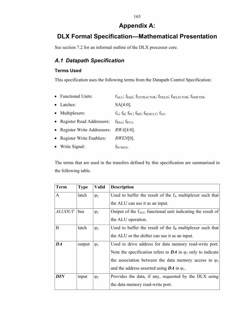
165
Appendix A: DLX Formal Specification—Mathematical Presentation
See section 7.2 for an informal outline of the DLX processor core.
A.1 Datapath Specification
Terms Used
This specification uses the following terms from the Datapath Control Specification:
• Functional Units: fALU; fEQZ; fEXTRACTOR; fFIELD; fSELECTOR; fSHIFTER.
• Latches: SA[4:0].
• Multiplexers: fA; fB; fPC; fRD; fRESULT; fSA'.
• Register Read Addressors: fRSA; fRTA.
• Register Write Addressors: RWA[4:0].
• Register Write Enablers: RWEN[0].
• Write Signal: fPCWEN.
The terms that are used in the transfers defined by this specification are summarised in
the following table.
Term Type Valid Description
A latch φ2 Used to buffer the result of the fA multiplexer such that
the ALU can use it as an input.
ALUOUT bus φ2 Output of the fALU functional unit indicating the result of
the ALU operation.
B latch φ2 Used to buffer the result of the fB multiplexer such that
the ALU or the shifter can use it as an input.
DA output φ1 Used to drive address for data memory read-write port.
Note the specification refers to DA in φ2 only to indicate
the association between the data memory access in φ2
and the address asserted using DA in φ1.
DIN input φ2 Provides the data, if any, requested by the DLX using
the data memory read-write port.
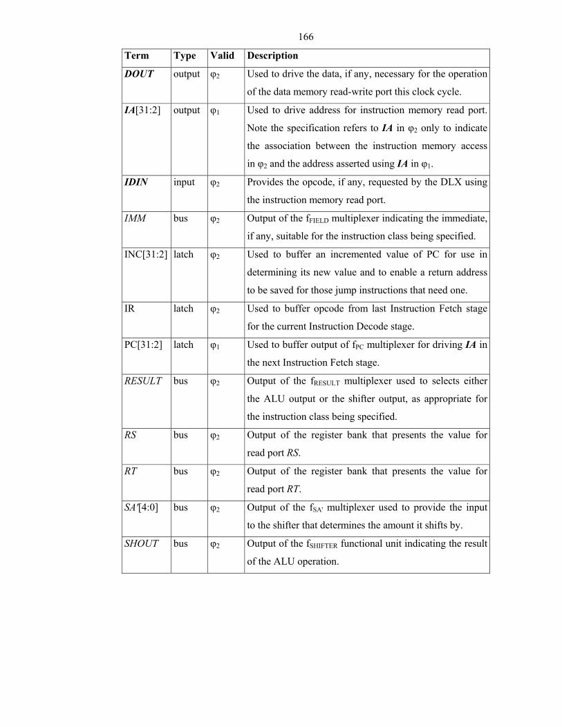
166
Term Type Valid Description
DOUT output φ2 Used to drive the data, if any, necessary for the operation
of the data memory read-write port this clock cycle.
IA[31:2] output φ1 Used to drive address for instruction memory read port.
Note the specification refers to IA in φ2 only to indicate
the association between the instruction memory access
in φ2 and the address asserted using IA in φ1.
IDIN input φ2 Provides the opcode, if any, requested by the DLX using
the instruction memory read port.
IMM bus φ2 Output of the fFIELD multiplexer indicating the immediate,
if any, suitable for the instruction class being specified.
INC[31:2] latch φ2 Used to buffer an incremented value of PC for use in
determining its new value and to enable a return address
to be saved for those jump instructions that need one.
IR latch φ2 Used to buffer opcode from last Instruction Fetch stage
for the current Instruction Decode stage.
PC[31:2] latch φ1 Used to buffer output of fPC multiplexer for driving IA in
the next Instruction Fetch stage.
RESULT bus φ2 Output of the fRESULT multiplexer used to selects either
the ALU output or the shifter output, as appropriate for
the instruction class being specified.
RS bus φ2 Output of the register bank that presents the value for
read port RS.
RT bus φ2 Output of the register bank that presents the value for
read port RT.
SA'[4:0] bus φ2 Output of the fSA' multiplexer used to provide the input
to the shifter that determines the amount it shifts by.
SHOUT bus φ2 Output of the fSHIFTER functional unit indicating the result
of the ALU operation.
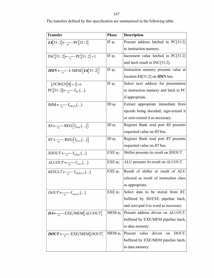
167
The transfers defined by this specification are summarised in the following table.
Transfer Phase Description
[ ] [ ]1
31: 2 PC 31: 2ϕ←IA IF φ1 Present address latched in PC[31:2]
to instruction memory.
[ ] [ ]1
INC 31: 2 PC 31: 2 1ϕ← + IF φ1 Increment value latched in PC[31:2]
and latch result in INC[31:2].
[ ]2
I- MEM 31: 2ϕ ← IDIN IA IF φ2 Instruction memory presents value at
location IA[31:2] on IDIN bus.
[ ]( )[ ] ( )
2 PC
0 1PC 31: 2 f
PCWEN
ϕ
= ⇒← …
IF φ2 Select next address for presentation
to instruction memory and latch in PC
if appropriate.
( )2 FIELDIMM fϕ← … ID φ2 Extract appropriate immediate from
opcode being decoded; sign-extend it
or zero-extend it as necessary.
( )2 RSAREG fRS ϕ← … ID φ2 Register Bank read port RS presents
requested value on RS bus.
( )2 RTAREG fRT ϕ← … ID φ2 Register Bank read port RT presents
requested value on RT bus.
( )2 shifterfSHOUT ϕ← … EXE φ2 Shifter presents its result on SHOUT.
( )2 ALUfALUOUT ϕ← … EXE φ2 ALU presents its result on ALUOUT.
( )2 RESULTfRESULT ϕ← … EXE φ2 Result of shifter or result of ALU
selected as result of instruction class
as appropriate.
( )2 selectorfDOUT ϕ← … EXE φ2 Select data to be stored from RT,
buffered by ID/EXE pipeline latch,
and zero-pad it to word as necessary.
[ ]1
EXE MEM ALUOUTϕ←DA MEM φ1 Present address driven on ALUOUT,
buffered by EXE/MEM pipeline latch,
to data memory.
[ ]1
EXE MEM DOUTϕ←DOUT MEM φ1 Present value driven on DOUT,
buffered by EXE/MEM pipeline latch,
to data memory.
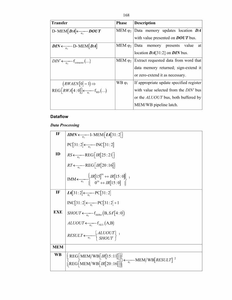
168
Transfer Phase Description
[ ]2
D- MEM ϕ←DA DOUT MEM φ2 Data memory updates location DA
with value presented on DOUT bus.
[ ]2
D- MEMϕ←DIN DA MEM φ2 Data memory presents value at
location DA[31:2] on DIN bus.
( )2 extractorfDIN ϕ
′← … MEM φ2 Extract requested data from word that
data memory returned; sign-extend it
or zero-extend it as necessary.
[ ]( )[ ] ( )
1 RD
0 1REG 4 : 0 f
RWAENRWA ϕ
= ⇒
← …
WB φ1 If appropriate update specified register
with value selected from the DIN' bus
or the ALUOUT bus, both buffered by
MEM/WB pipeline latch.
Dataflow
Data Processing
IF [ ]2
I- MEM 31: 2ϕ ← IDIN IA
[ ] [ ]2
PC 31: 2 INC 31: 2ϕ←
ID [ ]2
REG 25 : 21RS IRϕ ←
[ ]2
REG 20 :16RT IRϕ ←
[ ] [ ][ ]2
16
16
15 15 : 0IMM0 15: 0
IR IRIRϕ
++ ← ++
1
IF [ ] [ ]1
31: 2 PC 31: 2ϕ←IA
[ ] [ ]1
INC 31: 2 PC 31: 2 1ϕ← +
EXE [ ]( )2 shifterf B, 4 : 0SHOUT SAϕ
′←
( )2 ALUf A,BALUOUT ϕ←
2
ALUOUTRESULT SHOUTϕ ←
1
MEM
WB [ ][ ]
[ ]1
REG MEM WB 15 :11MEM WB
REG MEM WB 20 :16
IRRESULT
IR ϕ
←
2
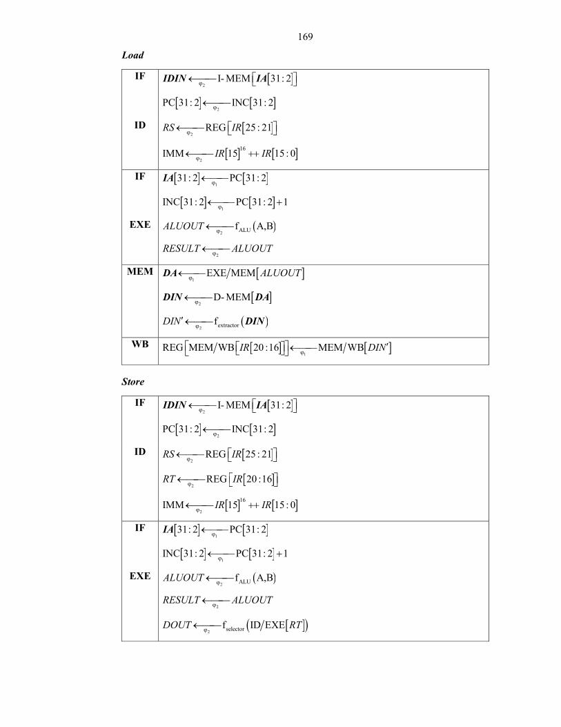
169
Load
IF [ ]2
I- MEM 31: 2ϕ ← IDIN IA
[ ] [ ]2
PC 31: 2 INC 31: 2ϕ←
ID [ ]2
REG 25 : 21RS IRϕ ←
[ ] [ ]2
16IMM 15 15 : 0IR IRϕ← ++
IF [ ] [ ]1
31: 2 PC 31: 2ϕ←IA
[ ] [ ]1
INC 31: 2 PC 31: 2 1ϕ← +
EXE ( )2 ALUf A,BALUOUT ϕ←
2RESULT ALUOUTϕ←
MEM [ ]1
EXE MEM ALUOUTϕ←DA
[ ]2
D- MEMϕ←DIN DA
( )2 extractorfDIN ϕ
′← DIN
WB [ ] [ ]1
REG MEM WB 20 :16 MEM WBIR DINϕ ′ ←
Store
IF [ ]2
I- MEM 31: 2ϕ ← IDIN IA
[ ] [ ]2
PC 31: 2 INC 31: 2ϕ←
ID [ ]2
REG 25 : 21RS IRϕ ←
[ ]2
REG 20 :16RT IRϕ ←
[ ] [ ]2
16IMM 15 15 : 0IR IRϕ← ++
IF [ ] [ ]1
31: 2 PC 31: 2ϕ←IA
[ ] [ ]1
INC 31: 2 PC 31: 2 1ϕ← +
EXE ( )2 ALUf A,BALUOUT ϕ←
2RESULT ALUOUTϕ←
[ ]( )2 selectorf ID EXEDOUT RTϕ←
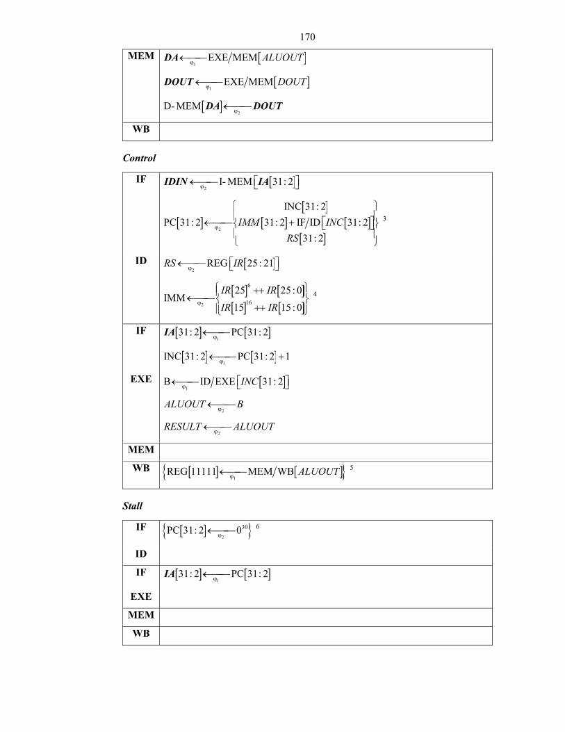
170
MEM [ ]1
EXE MEM ALUOUTϕ←DA
[ ]1
EXE MEM DOUTϕ←DOUT
[ ]2
D- MEM ϕ←DA DOUT
WB
Control
IF [ ]2
I- MEM 31: 2ϕ ← IDIN IA
[ ][ ]
[ ] [ ][ ]
2
INC 31: 2PC 31: 2 31: 2 IF ID 31: 2
31: 2IMM INC
RSϕ
← +
3
ID [ ]2
REG 25 : 21RS IRϕ ←
[ ] [ ][ ] [ ]2
6
16
25 25 : 0IMM
15 15 : 0
IR IR
IR IRϕ
++ ← ++
4
IF [ ] [ ]1
31: 2 PC 31: 2ϕ←IA
[ ] [ ]1
INC 31: 2 PC 31: 2 1ϕ← +
EXE [ ]1
B ID EXE 31: 2INCϕ ←
2ALUOUT Bϕ←
2RESULT ALUOUTϕ←
MEM
WB [ ] [ ]{ }1
REG 11111 MEM WB ALUOUTϕ← 5
Stall
IF [ ]{ }2
30PC 31: 2 0ϕ← 6
ID
IF [ ] [ ]1
31: 2 PC 31: 2ϕ←IA
EXE
MEM
WB
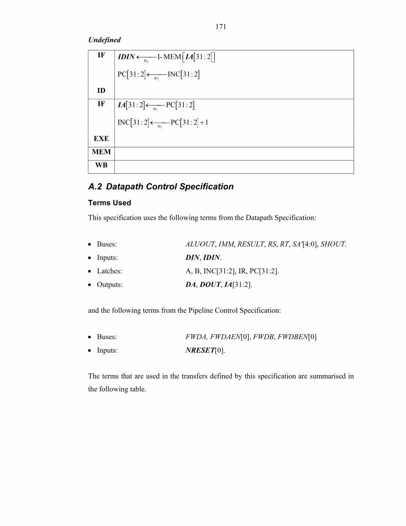
171
Undefined
IF [ ]2
I- MEM 31: 2ϕ ← IDIN IA
[ ] [ ]2
PC 31: 2 INC 31: 2ϕ←
ID
IF [ ] [ ]1
31: 2 PC 31: 2ϕ←IA
[ ] [ ]1
INC 31: 2 PC 31: 2 1ϕ← +
EXE
MEM
WB
A.2 Datapath Control Specification
Terms Used
This specification uses the following terms from the Datapath Specification:
• Buses: ALUOUT, IMM, RESULT, RS, RT, SA'[4:0], SHOUT.
• Inputs: DIN, IDIN.
• Latches: A, B, INC[31:2], IR, PC[31:2].
• Outputs: DA, DOUT, IA[31:2].
and the following terms from the Pipeline Control Specification:
• Buses: FWDA, FWDAEN[0], FWDB, FWDBEN[0]
• Inputs: NRESET[0].
The terms that are used in the transfers defined by this specification are summarised in
the following table.
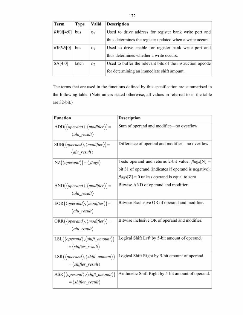
172
Term Type Valid Description
RWA[4:0] bus φ1 Used to drive address for register bank write port and
thus determines the register updated when a write occurs.
RWEN[0] bus φ1 Used to drive enable for register bank write port and
thus determines whether a write occurs.
SA[4:0] latch φ2 Used to buffer the relevant bits of the instruction opcode
for determining an immediate shift amount.
The terms that are used in the functions defined by this specification are summarised in
the following table. (Note unless stated otherwise, all values in referred to in the table
are 32-bit.)
Function Description
( )ADD ,operand modifier
alu_result
=
Sum of operand and modifier—no overflow.
( )SUB ,operand modifier
alu_result
=
Difference of operand and modifier—no overflow.
( )NZ operand flags= Tests operand and returns 2-bit value: flags[N] =
bit 31 of operand (indicates if operand is negative);
flags[Z] = 0 unless operand is equal to zero.
( )AND ,operand modifier
alu_result
=
Bitwise AND of operand and modifier.
( )EOR ,operand modifier
alu_result
=
Bitwise Exclusive OR of operand and modifier.
( )ORR ,operand modifier
alu_result
=
Bitwise inclusive OR of operand and modifier.
( )LSL ,operand shift_amount
shifter_result=
Logical Shift Left by 5-bit amount of operand.
( )LSR ,operand shift_amount
shifter_result=
Logical Shift Right by 5-bit amount of operand.
( )ASR ,operand shift_amount
shifter_result=
Arithmetic Shift Right by 5-bit amount of operand.
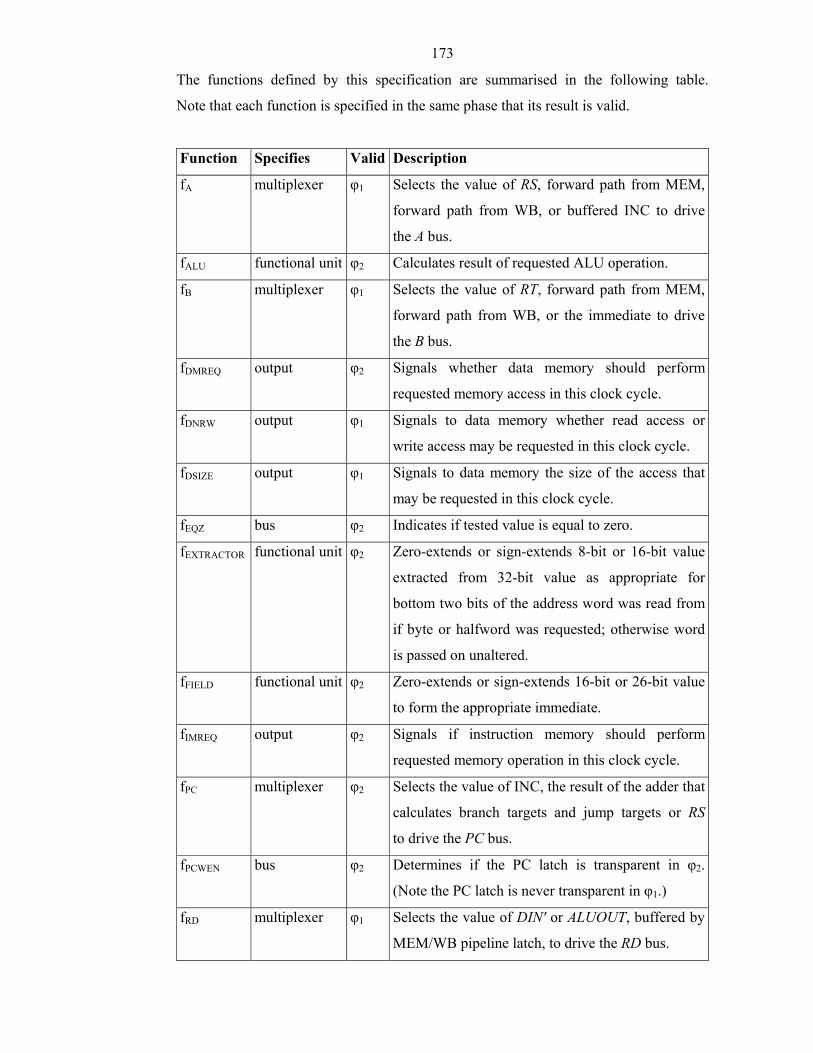
173
The functions defined by this specification are summarised in the following table.
Note that each function is specified in the same phase that its result is valid.
Function Specifies Valid Description
fA multiplexer φ1 Selects the value of RS, forward path from MEM,
forward path from WB, or buffered INC to drive
the A bus.
fALU functional unit φ2 Calculates result of requested ALU operation.
fB multiplexer φ1 Selects the value of RT, forward path from MEM,
forward path from WB, or the immediate to drive
the B bus.
fDMREQ output φ2 Signals whether data memory should perform
requested memory access in this clock cycle.
fDNRW output φ1 Signals to data memory whether read access or
write access may be requested in this clock cycle.
fDSIZE output φ1 Signals to data memory the size of the access that
may be requested in this clock cycle.
fEQZ bus φ2 Indicates if tested value is equal to zero.
fEXTRACTOR functional unit φ2 Zero-extends or sign-extends 8-bit or 16-bit value
extracted from 32-bit value as appropriate for
bottom two bits of the address word was read from
if byte or halfword was requested; otherwise word
is passed on unaltered.
fFIELD functional unit φ2 Zero-extends or sign-extends 16-bit or 26-bit value
to form the appropriate immediate.
fIMREQ output φ2 Signals if instruction memory should perform
requested memory operation in this clock cycle.
fPC multiplexer φ2 Selects the value of INC, the result of the adder that
calculates branch targets and jump targets or RS
to drive the PC bus.
fPCWEN bus φ2 Determines if the PC latch is transparent in φ2.
(Note the PC latch is never transparent in φ1.)
fRD multiplexer φ1 Selects the value of DIN' or ALUOUT, buffered by
MEM/WB pipeline latch, to drive the RD bus.
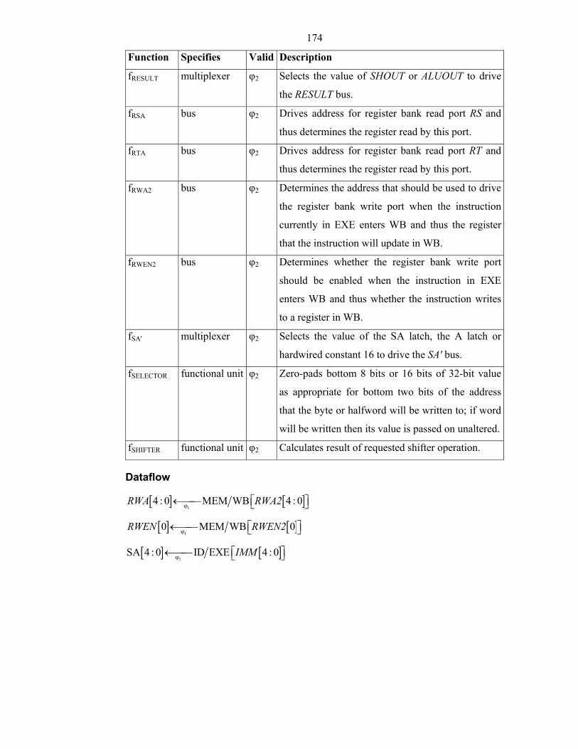
174
Function Specifies Valid Description
fRESULT multiplexer φ2 Selects the value of SHOUT or ALUOUT to drive
the RESULT bus.
fRSA bus φ2 Drives address for register bank read port RS and
thus determines the register read by this port.
fRTA bus φ2 Drives address for register bank read port RT and
thus determines the register read by this port.
fRWA2 bus φ2 Determines the address that should be used to drive
the register bank write port when the instruction
currently in EXE enters WB and thus the register
that the instruction will update in WB.
fRWEN2 bus φ2 Determines whether the register bank write port
should be enabled when the instruction in EXE
enters WB and thus whether the instruction writes
to a register in WB.
fSA' multiplexer φ2 Selects the value of the SA latch, the A latch or
hardwired constant 16 to drive the SA' bus.
fSELECTOR functional unit φ2 Zero-pads bottom 8 bits or 16 bits of 32-bit value
as appropriate for bottom two bits of the address
that the byte or halfword will be written to; if word
will be written then its value is passed on unaltered.
fSHIFTER functional unit φ2 Calculates result of requested shifter operation.
Dataflow
[ ] [ ]1
4 : 0 MEM WB 4 : 0RWA RWA2ϕ ←
[ ] [ ]1
0 MEM WB 0RWEN RWEN2ϕ ←
[ ] [ ]1
SA 4 : 0 ID EXE 4 : 0IMMϕ ←
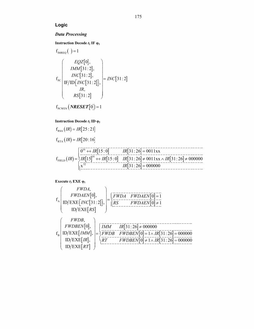
175
Logic
Data Processing
Instruction Decode t2 IF φ2
( )IMREQf 1=
[ ][ ][ ]
[ ]
[ ]
[ ]PC
0 ,31: 2 ,31: 2 ,
f 31: 2IF ID 31: 2 ,
,31: 2
EQZIMMINC
INCINC
IRRS
=
[ ]( )PCWENf 0 1=NRESET
Instruction Decode t2 ID φ2
( ) [ ]RSAf 25 : 21IR IR=
( ) [ ]RTAf 20 :16IR IR=
( )[ ] [ ]
[ ] [ ] [ ] [ ][ ]
16
16FIELD
32
0 15 : 0 31: 26 0011xx
f 15 15 : 0 31: 26 0011xx 31: 26 000000x 31: 26 000000
IR IR
IR IR IR IR IRIR
++ == ++ ≠ ∧ ≠ =
Execute t3 EXE φ1
[ ][ ]
[ ]
[ ][ ]A
,0 , 0 1
f ID EXE 31: 2 , 0 1ID EXE
FWDAFWDAEN FWDA FWDAEN
INC RS FWDAENRS
= = ≠
[ ][ ]
[ ][ ]
[ ][ ] [ ][ ] [ ]
B
,0 , 31: 26 000000
ID EXE ,f 0 1 31: 26 000000ID EXE , 0 1 31: 26 000000ID EXE
FWDBFWDBEN IMM IR
IMM FWDB FWDBEN IRIR RT FWDBEN IRRT
≠
= = ∧ = ≠ ∧ =
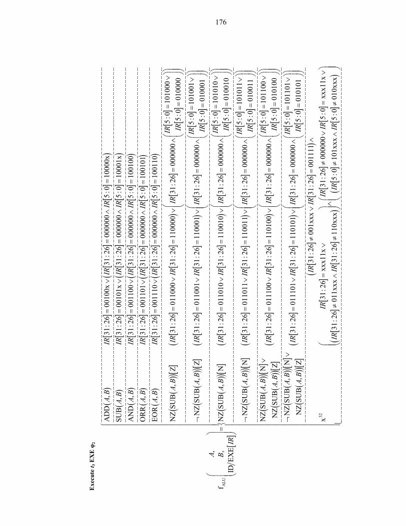
176
Exe
cute
t 3 E
XE
φ2 [
]
()
[]
[]
[]
()
()
[]
[]
[]
()
()
[]
[]
[]
()
()
[]
[]
ALU
AD
D,
31:2
600
100x
31:2
600
0000
5:0
1000
0xSU
B,
31:2
600
101x
31:2
600
0000
5:0
1000
1xA
ND
,31
:26
0011
0031
:26
0000
005:
010
0100
OR
R,
31:2
600
1101
31:2
60
,f
,ID
EXE
AB
IRIR
IRA
BIR
IRIR
AB
IRIR
IRA
BIR
IR
A BIR
=∨
=∧
=
=∨
=∧
=
=∨
=∧
=
=∨
=
=
[]
()
()
[]
[]
[]
()
()
()[
][
][
](
)[
][
][
]
()
()[
][
][
](
)
0000
05:
010
0101
EOR
,31
:26
0011
1031
:26
0000
005:
010
0110
5:0
1010
00N
ZSU
B,
Z31
:26
0110
0031
:26
1100
0031
:26
0000
005:
001
0000
NZ
SUB
,Z
31:2
601
1001
31:2
611
0001
IRA
BIR
IRIR
IRA
BIR
IRIR
IR
AB
IRIR
I
∧=
=∨
=∧
=
=∨
=∨
=∨
=∧
=
¬=
∨=
∨[
][
][
]
()
()[
][
][
](
)[
][
][
]
()
()[
][
][
](
)[
]
5:0
1010
0131
:26
0000
005:
001
0001
5:0
1010
10N
ZSU
B,
N31
:26
0110
1031
:26
1100
1031
:26
0000
005:
001
0010
NZ
SUB
,N
31:2
601
1011
31:2
611
0011
31:2
600
0000
IRR
IR IRA
BIR
IRIR
IR
AB
IRIR
IR
=∨
=∧
=
=
∨=
∨=
∨=
∧
=
¬=
∨=
∨=
[]
[]
()
()[
](
)(
)[]
[]
[]
()
[]
[]
[]
()
()[
](
)(
)[]
[]
[]
()
[]
5:0
1010
115:
001
0011
NZ
SUB
,N
5:0
1011
0031
:26
0111
0031
:26
1101
0031
:26
0000
005:
001
0100
NZ
SUB
,Z
NZ
SUB
,N
31:2
601
1101
31:2
611
0101
31:2
6N
ZSU
B,
Z
IR IR
AB
IRIR
IRIR
IRA
BA
BIR
IRIR
AB
=∨
∧
=
∨
=
∨=
∨=
∨=
∧
=
¬∨
=∨
=∨
[]
[]
[]
[]
()
[]
[]
[]
()
[]
[]
[]
[]
()
32
5:0
1011
0100
0000
5:0
0101
01
31:2
600
1xxx
31:2
600
1111
x31
:26
xxx1
1x31
:26
0000
005:
0xx
x11x
31:2
601
1xxx
31:2
611
0xxx
5:0
101x
xx5:
001
0xxx
IR IR
IRIR
IRIR
IRIR
IRIR
IR
=∨
=∧
=
≠
∨=
∧
=∨
≠∨
=∨
∧
≠
∧≠
≠∧
≠
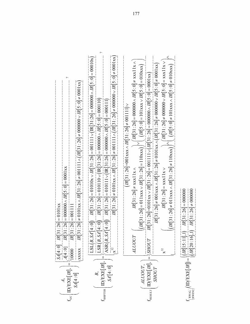
177
[]
[]
[]
[]
[]
[]
[]
[]
[]
[]
[]
()
SA
4:0
31:2
601
01xx
,[4
:0]
31:2
600
0000
5:0
0001
xxf
IDEX
E,
1000
031
:26
0011
114:
0xx
xxx
31:2
601
01xx
31:2
600
1111
31:2
600
0000
5:0
0001
xx
SAIR
AA
IRIR
IRIR
SAIR
IRIR
IR
′
=
=
∧=
=
=
≠
∧≠
∧≠
∨≠
7
[]
[]
[]
()
[]
[]
[]
[]
()
[]
()
[]
[]
[]
()
[]
()
[]
[]
SHIF
TER
LSL
,4:
031
:26
0101
0x31
:26
0011
11IR
31:2
600
0000
5:0
0001
0x,
LSR
,4:
031
:26
0101
10IR
31:2
600
0000
5:0
0001
10f
IDEX
E,
ASR
,4:
031
:26
0101
11IR
31:2
600
0000
54:
0
BSA
IRIR
IRB
BSA
IRIR
IRB
SAIR
IRSA
′=
∨=
∨=
∧=
′=
∨=
∧=
=
′=
∨=
∧
′
[]
()
[]
[]
[]
[]
()
32
:000
0111
x31
:26
0101
xx31
:26
0011
1131
:26
0000
005:
000
01xx
IRIR
IRIR
=
≠
∧≠
∧≠
∨≠
7
[]
[]
[]
()
[]
[]
[]
()
[]
[]
[]
[]
()
[]
RES
ULT
31:2
6=0
01xx
x31
:26
0011
1131
:26
xxx1
1x31
:26
0000
005:
0xx
x11x
31:2
601
1xxx
31:2
611
0xxx
5:0
101x
xx5:
001
0xxx
,f
IDEX
E,
31:2
6
IRIR
ALU
OU
TIR
IRIR
IRIR
IRIR
ALU
OU
T IRSH
OU
TIR
SHO
UT
∧≠
∨
≠∧
=∧
≠∧
∨
=
∨=
=∨
=
=
[
][
][
](
)[
][
][
][
](
)[
][
][
](
)[
][
][
]32
=010
1xx
31:2
600
1111
31:2
600
0000
5:0
0001
xx31
:26
001x
xx31
:26
0101
xx31
:26
0000
005:
000
01xx
x31
:26
xxx1
1x31
:26
0000
005:
0xx
x11x
31:2
601
1xxx
31:2
611
0xxx
5:0
101
IRIR
IRIR
IRIR
IRIR
IRIR
IRIR
IR
∨=
∨=
∧=
≠∧
≠∧
≠∨
≠
=∨
≠∨
=∨
∧
≠
∧≠
≠
[
](
)xx
x5:
001
0xxx
IR
∧
∧≠
[]
()
[]
()
[]
[]
()
[]
RW
A2,
RW
EN2
15:1
1,1
31:2
600
0000
fID
EXE
20:1
6,1
31:2
600
0000
IRIR
IRIR
IR
=
=
≠
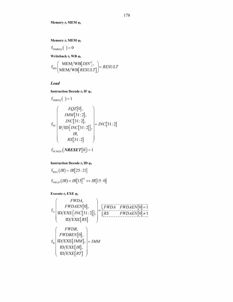
178Memory t3 MEM φ1
Memory t3 MEM φ2
( )DMREQf 0=
Writeback t3 WB φ1
[ ][ ]RD
MEM WB ,f
MEM WBDIN
RESULTRESULT
′ =
Load
Instruction Decode t3 IF φ2
( )IMREQf 1=
[ ][ ][ ]
[ ]
[ ]
[ ]PC
0 ,31: 2 ,31: 2 ,
f 31: 2IF ID 31: 2 ,
,31: 2
EQZIMMINC
INCINC
IRRS
=
[ ]( )PCWENf 0 1=NRESET
Instruction Decode t3 ID φ2
( ) [ ]RSAf 25 : 21IR IR=
( ) [ ] [ ]16FIELDf 15 15 : 0IR IR IR= ++
Execute t3 EXE φ1
[ ][ ]
[ ]
[ ][ ]A
,0 , 0 1
f ID EXE 31: 2 , 0 1ID EXE
FWDAFWDAEN FWDA FWDAEN
INC RS FWDAENRS
= = ≠
[ ][ ]
[ ][ ]
B
,0 ,
ID EXE ,fID EXE ,ID EXE
FWDBFWDBEN
IMM IMMIRRT
=
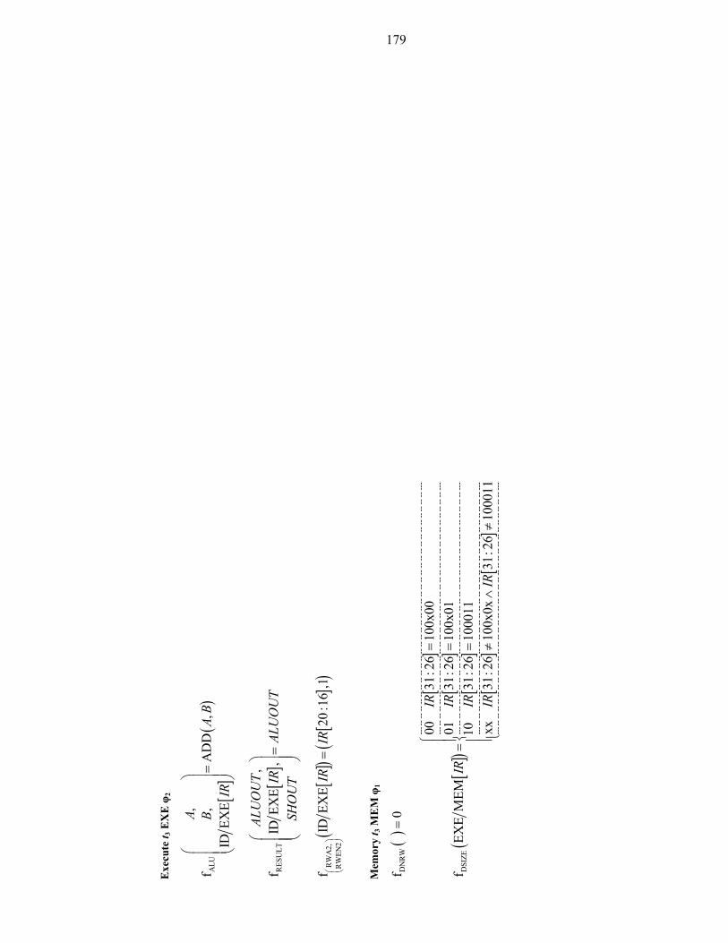
179
Exe
cute
t 3 E
XE
φ2 [
](
)A
LU
,f
,A
DD
,ID
EXEA B
AB
IR
=
[]
RES
ULT
,f
IDEX
E,
ALU
OU
T IRAL
UO
UT
SHO
UT
=
[]
()
[]
()
RW
A2,
RW
EN2
fID
EXE
20:1
6,1
IRIR
=
Mem
ory
t 3 M
EM
φ1
()D
NR
Wf
0=
[]
()
[]
[]
[]
[]
[]
DSI
ZE
0031
:26
100x
0001
31:2
610
0x01
fEX
EM
EM10
31:2
610
0011
xx31
:26
100x
0x31
:26
1000
11
IR IRIR
IR IRIR
=
=
=
=
≠
∧≠
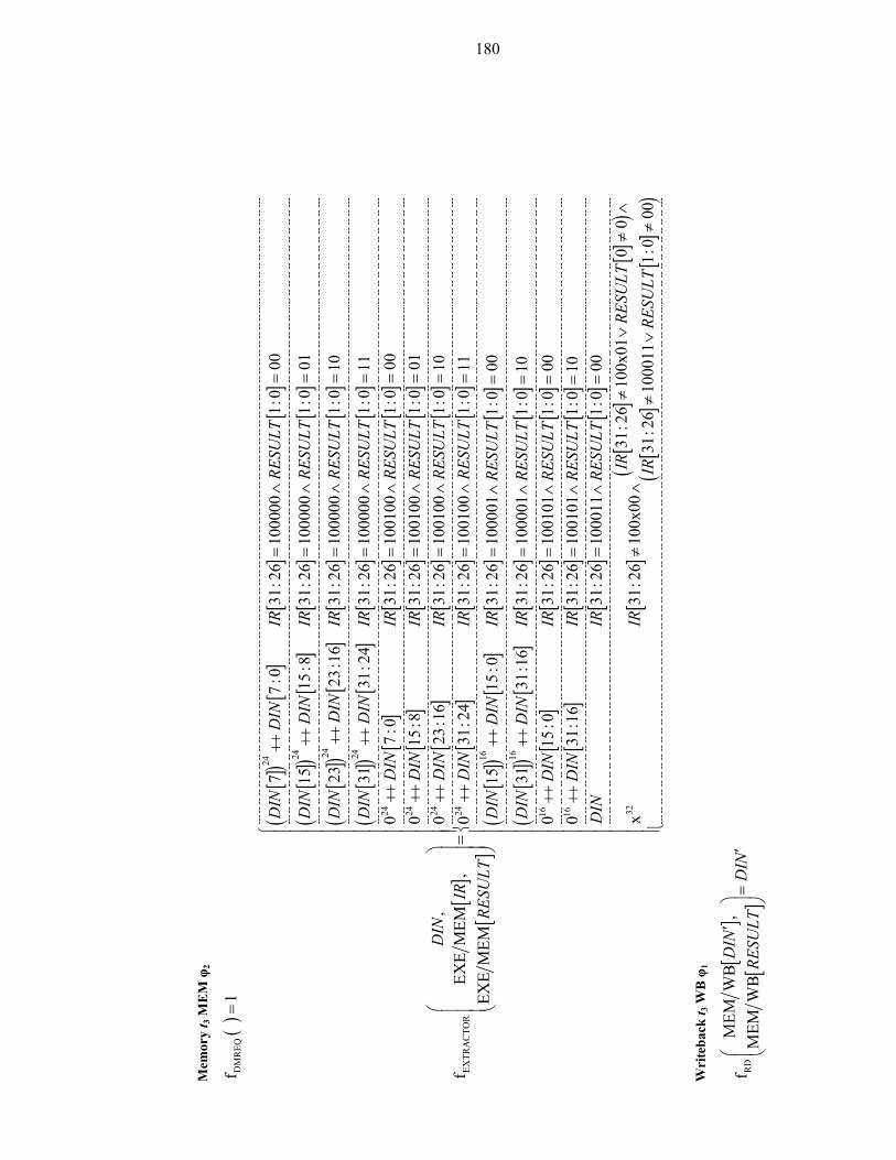
180
Mem
ory
t 3 M
EM
φ2
()D
MR
EQf
1=
[]
[]
[](
)[
][
][
][
](
)[
][
][
][
](
)[
][
][
][
](
)[
][
]
24 24 24 24
EXTR
AC
TOR
77:
031
:26
1000
001:
000
1515
:831
:26
1000
001:
001
2323
:16
31:2
610
0000
1:0
10
3131
:24
31:2
61
,f
EXE
MEM
,EX
EM
EM
DIN
DIN
IRRE
SULT
DIN
DIN
IRRE
SULT
DIN
DIN
IRRE
SULT
DIN
DIN
IR
DIN
IRRE
SULT
++=
∧=
++=
∧=
++=
∧=
++=
=
[]
[]
[]
[]
[]
[]
[]
[]
[]
[]
[]
[]
[]
[]
()
[]
[]
24 24 24 24
16
0000
01:
011
07:
031
:26
1001
001:
000
015
:831
:26
1001
001:
001
023
:16
31:2
610
0100
1:0
100
31:2
431
:26
1001
001:
011
1515
:031
:26
1
RESU
LTD
INIR
RESU
LTD
INIR
RESU
LTD
INIR
RESU
LTD
INIR
RESU
LT
DIN
DIN
IR
∧=
++=
∧=
++=
∧=
++=
∧=
++=
∧=
++=
[]
[]
()
[]
[]
[]
[]
[]
[]
[]
[]
[]
[]
[]
[]
[]
16
16 16 32
0000
11:
000
3131
:16
31:2
610
0001
1:0
100
15:0
31:2
610
0101
1:0
000
31:1
631
:26
1001
011:
010
31:2
610
0011
1:0
0031
:26
100
x31
:26
100x
00
RESU
LT
DIN
DIN
IRRE
SULT
DIN
IRRE
SULT
DIN
IRRE
SULT
DIN
IRRE
SULT
IRIR
∧=
++=
∧=
++=
∧=
++=
∧=
=∧
=≠
≠∧
[](
)[
][
](
)x0
10
031
:26
1000
111:
000
RESU
LTIR
RESU
LT
∨
≠∧
≠
∨≠
Wri
teba
ck t 3
WB
φ1 [
][
]R
D
MEM
WB
,f
MEM
WB
DIN
DIN
RESU
LT′
′
=
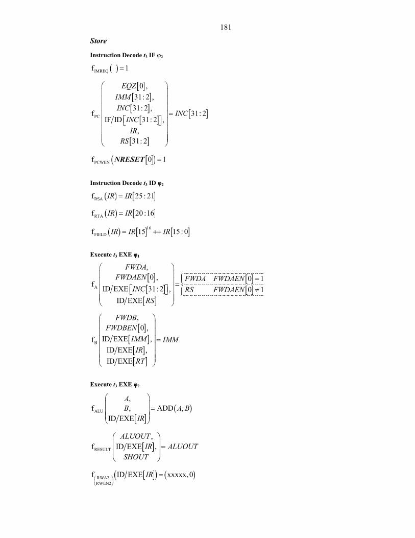
181
Store
Instruction Decode t3 IF φ2
( )IMREQf 1=
[ ][ ][ ]
[ ]
[ ]
[ ]PC
0 ,31: 2 ,31: 2 ,
f 31: 2IF ID 31: 2 ,
,31: 2
EQZIMMINC
INCINC
IRRS
=
[ ]( )PCWENf 0 1=NRESET
Instruction Decode t3 ID φ2
( ) [ ]RSAf 25 : 21IR IR=
( ) [ ]RTAf 20 :16IR IR=
( ) [ ] [ ]16FIELDf 15 15 : 0IR IR IR= ++
Execute t3 EXE φ1
[ ][ ]
[ ]
[ ][ ]A
,0 , 0 1
f ID EXE 31: 2 , 0 1ID EXE
FWDAFWDAEN FWDA FWDAEN
INC RS FWDAENRS
= = ≠
[ ][ ]
[ ][ ]
B
,0 ,
ID EXE ,fID EXE ,ID EXE
FWDBFWDBEN
IMM IMMIRRT
=
Execute t3 EXE φ2
[ ]( )ALU
,f , ADD ,
ID EXE
AB A B
IR
=
[ ]RESULT
,f ID EXE ,
ALUOUTIR ALUOUT
SHOUT
=
[ ]( ) ( )RWA2,RWEN2
f ID EXE xxxxx,0IR
=
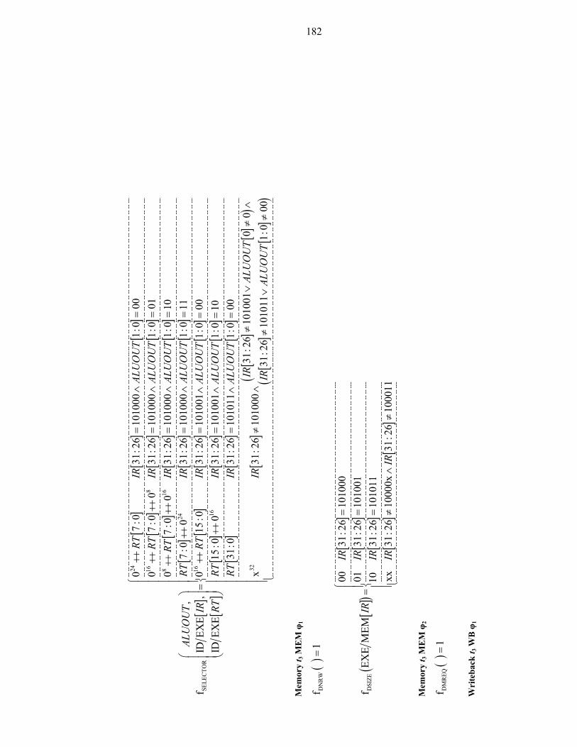
182
[]
[]
[]
[]
[]
[]
[]
[]
[]
[]
[]
[]
[]
[]
24 168
816
24
1SE
LEC
TOR
07
:031
:26
1010
001:
000
07
:00
31:2
610
1000
1:0
010
7:0
031
:26
1010
001:
010
7:0
031
:26
1010
001:
011
,0
fID
EXE
,ID
EXE
RTIR
ALU
OU
TRT
IRAL
UO
UT
RTIR
ALU
OU
TRT
IRAL
UO
UT
ALU
OU
T IR RT
++=
∧=
++++
=∧
=++
++=
∧=
++=
∧=
=
[]
[]
[]
[]
[]
[]
[]
[]
[]
[]
[]
[](
)[
][
](
)
6
16
32
15:0
31:2
610
1001
1:0
0015
:00
31:2
610
1001
1:0
1031
:031
:26
1010
111:
000
31:2
610
1001
00
x31
:26
1010
0031
:26
1010
111:
000
RTIR
ALU
OU
TRT
IRAL
UO
UT
RTIR
ALU
OU
TIR
ALU
OU
TIR
IRAL
UO
UT
++
=∧
=
++=
∧=
=
∧=
≠
∨≠
∧
≠∧
≠
∨≠
Mem
ory
t 3 M
EM
φ1
()D
NR
Wf
1=
[]
()
[]
[]
[]
[]
[]
DSI
ZE
0031
:26
1010
0001
31:2
610
1001
fEX
EM
EM10
31:2
610
1011
xx31
:26
1000
0x31
:26
1000
11
IR IRIR
IR IRIR
=
=
=
=
≠
∧≠
Mem
ory
t 3 M
EM
φ2
()D
MR
EQf
1=
Wri
teba
ck t 3
WB
φ1
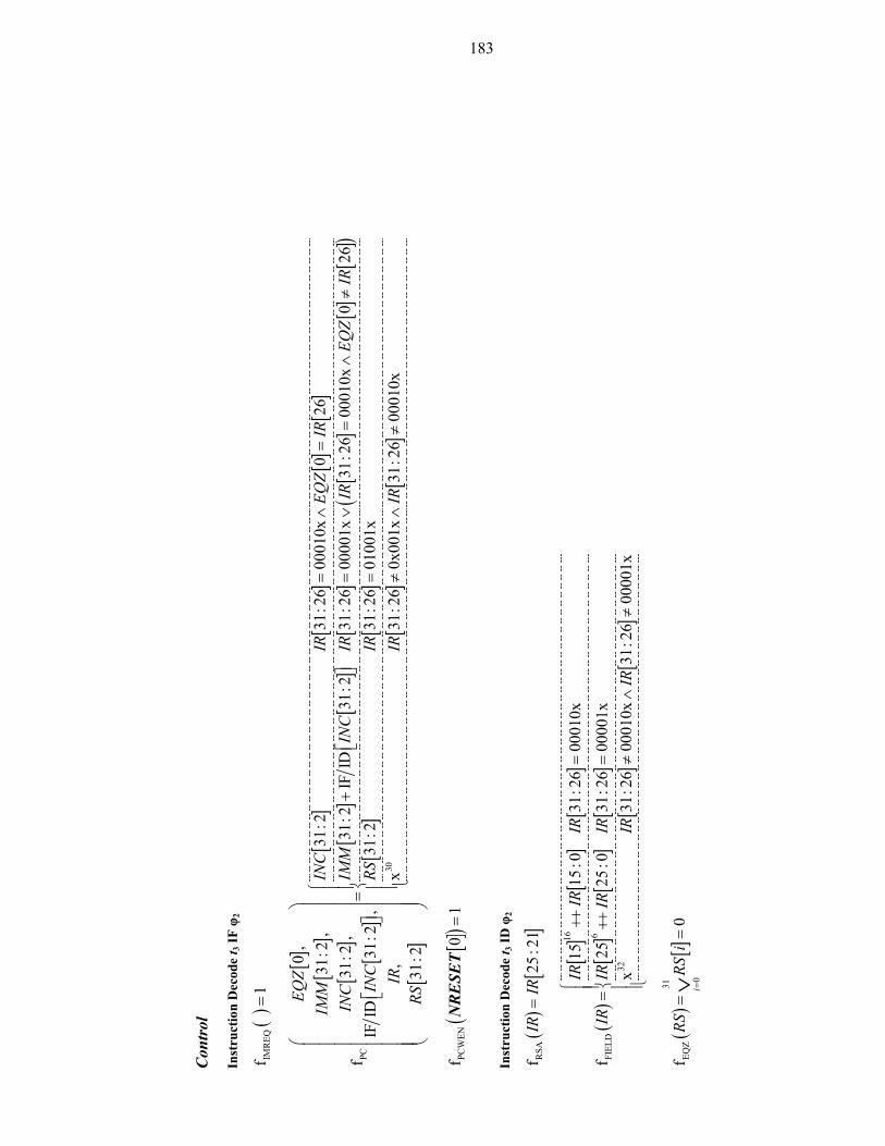
183
Con
trol
Inst
ruct
ion
Dec
ode
t 3 IF
φ2
()IM
REQ
f1
=
[] []
[]
[]
[]
[]
[]
[][
][
][
][
][
][]
[]
()
[]
[]
[]
PC
30
0,
31:2
31:2
600
010x
026
31:2
,31
:2IF
ID31
:231
:26
0000
1x31
:26
0001
0x0
2631
:2,
f31
:231
:26
0100
1xIF
ID31
:2,
,x
31:2
60x
001x
31:2
EQZ
INC
IREQ
ZIR
IMM
IMM
INC
IRIR
EQZ
IRIN
CRS
IRIN
C IRIR
RS
=∧
=
+
=∨
=∧
≠
=
=
≠
[]
31:2
600
010x
IR
∧
≠
[](
)PC
WEN
f0
1=
NR
ESE
T
Inst
ruct
ion
Dec
ode
t 3 ID
φ2
()
[]
RSA
f25
:21
IRIR
=
()
[]
[]
[]
[]
[]
[]
[]
[]
16 6FI
ELD
32
1515
:031
:26
0001
0x
f25
25:0
31:2
600
001x
x31
:26
0001
0x31
:26
0000
1x
IRIR
IR
IRIR
IRIR IR
IR
++
=
=++
=
≠∧
≠
()
[]31
EQZ
0f
0i
RSRS
i=
==
∨
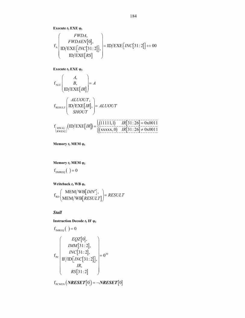
184
Execute t3 EXE φ1
[ ][ ]
[ ]
[ ]A
,0 ,
f ID EXE 31: 2 00ID EXE 31: 2 ,ID EXE
FWDAFWDAEN
INCINCRS
= ++
Execute t3 EXE φ2
[ ]ALU
,f ,
ID EXE
AB A
IR
=
[ ]RESULT
,f ID EXE ,
ALUOUTIR ALUOUT
SHOUT
=
[ ]( ) ( ) [ ]( ) [ ]RWA2,
RWEN2
11111,1 31: 26 0x0011f ID EXE
xxxxx,0 31: 26 0x0011IR
IRIR
== ≠
Memory t3 MEM φ1
Memory t3 MEM φ2
( )DMREQf 0=
Writeback t3 WB φ1
[ ][ ]RD
MEM WB ,f
MEM WBDIN
RESULTRESULT
′ =
Stall
Instruction Decode t3 IF φ2
( )IMREQf 0=
[ ][ ][ ]
[ ]
[ ]
30PC
0 ,31: 2 ,31: 2 ,
f 0IF ID 31: 2 ,
,31: 2
EQZIMMINC
INCIR
RS
=
[ ]( ) [ ]PCWENf 0 0= ¬NRESET NRESET
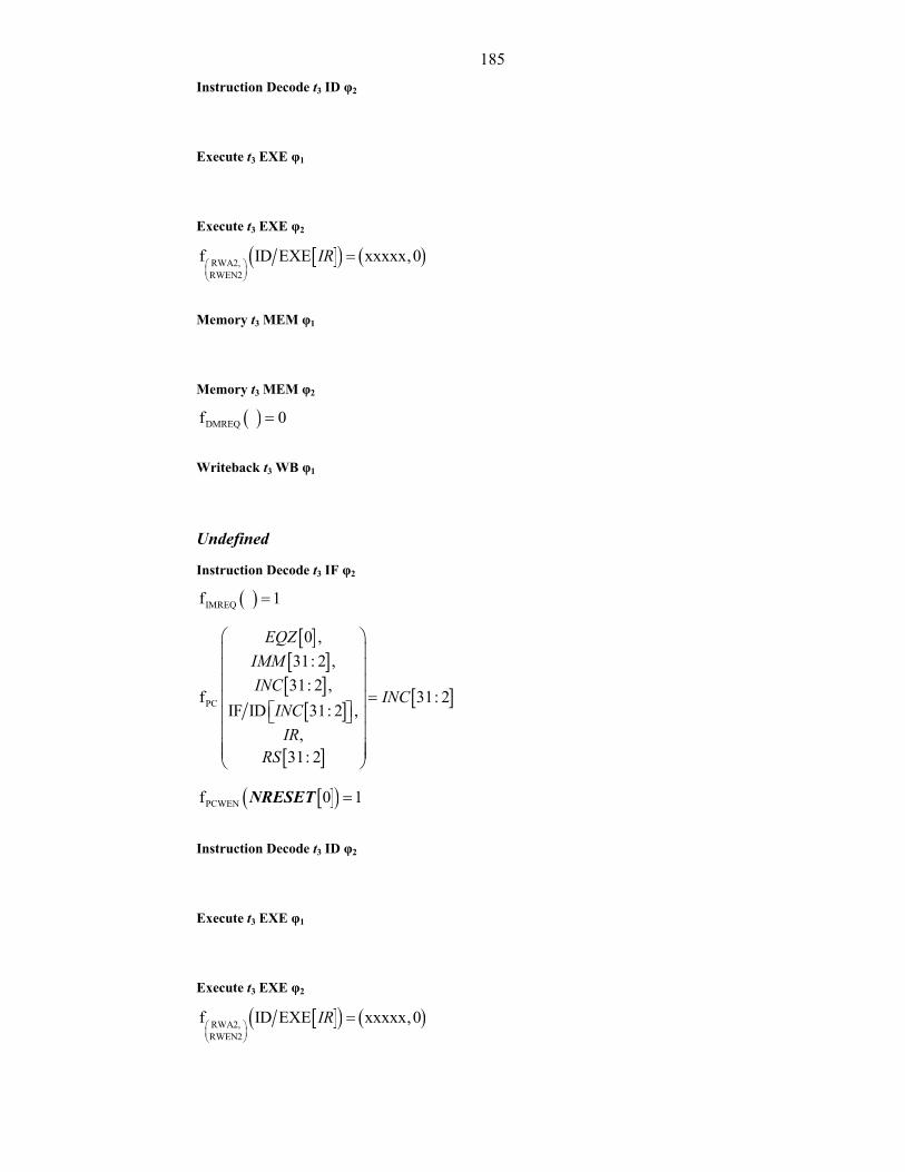
185Instruction Decode t3 ID φ2
Execute t3 EXE φ1
Execute t3 EXE φ2
[ ]( ) ( )RWA2,RWEN2
f ID EXE xxxxx,0IR
=
Memory t3 MEM φ1
Memory t3 MEM φ2
( )DMREQf 0=
Writeback t3 WB φ1
Undefined
Instruction Decode t3 IF φ2
( )IMREQf 1=
[ ][ ][ ]
[ ]
[ ]
[ ]PC
0 ,31: 2 ,31: 2 ,
f 31: 2IF ID 31: 2 ,
,31: 2
EQZIMMINC
INCINC
IRRS
=
[ ]( )PCWENf 0 1=NRESET
Instruction Decode t3 ID φ2
Execute t3 EXE φ1
Execute t3 EXE φ2
[ ]( ) ( )RWA2,RWEN2
f ID EXE xxxxx,0IR
=
186Memory t3 MEM φ1
Memory t3 MEM φ2
( )DMREQf 0=
Writeback t3 WB φ1
A.3 Pipeline Control Specification
Terms Used
This specification uses the following terms from the Datapath specification:
• Inputs: IDIN.
• Latches: IR.
This specification uses the following terms from the Datapath Control specification:
• Buses: RD, RESULT, RWA2[4:0], RWEN2[0].
• Register Read Addressors: fRSA; fRTA.
• Register Write Addressors: RWA[4:0].
• Register Write Enablers: RWEN[0].
The terms that are used in the transfers defined by this specification are summarised in
the following table.
Term Type Valid Description
IC[*] special φ1, φ2 The instruction class that should be associated with
the instruction in EXE this clock cycle.
NRESET[0] input φ2 External input that indicates when any instructions in
the pipeline should be ignored and the program counter
should be reset to 0x00000000.
The functions defined by this specification are summarised in the following table.
Note that each function is specified in the same phase that its result is valid.
187
Function Specifies Valid Description
fFWDA bus φ1 Presents value of forward path the fA multiplexer
should use as selection option.
fFWDAEN bus φ1 Indicates when the fA multiplexer would select
value read from RS register bank read port whether
it should select value presented by fFWDA instead.
fFWDB bus φ1 Presents value of forward path the fB multiplexer
should use as selection option.
fFWDBEN bus φ1 Indicates when the fB multiplexer would select
value read from RT register bank read port whether
it should select value presented by fFWDB instead.
fIRWRITE bus φ2 Determines whether to update opcode latched in IR
or not—if stall should be inserted into pipeline,
update should not occur.
fNXTIC special φ2 The instruction class that should be associated with
the instruction in ID this clock cycle.
fSTALL bus φ2 Indicates when data hazard has been detected by
hazard unit and stall must be inserted into pipeline.
Dataflow
• IDEC control logic:
[ ] [ ]1φ
IC * *NXTIC←
• PIPE control logic:
[ ] [ ]1φ
* IR IF IDIRWRITE IDIN⇒ ←
188
Forw
ardi
ng L
ogic
ϕ 1
[]
[]
[]
[]
[][]
()
[][
][
](
)[]
[]
FWD
A,
FWD
AEN
,EX
EM
EM0
1EX
EM
EM4:
0ID
EXE
4:0
EXE
MEM
,,1
IDEX
E4:
0,
01
4:0
IDEX
E4:
0,
fEX
EM
EM4:
0,
0,
EXE
MEM
0
RDRW
EN2
RWA2
RSA
RESU
LTRD
RSA
RWEN
RWA
RRW
ARW
A2RW
ENRW
EN2
≠∨
≠∧
=∧
=
=
[]
[]
()
[][
][
]
()
[][
][
](
)[]
[]
[]
()
4:0
EXE
MEM
,1EX
EM
EM0
1EX
EM
EM4:
0ID
EXE
4:0
EXE
MEM
01
EXE
MEM
4:0
IDEX
E4:
0xx
xx,0
01
4:0
IDEX
E4:
0
SARE
SULT
RWEN
2RW
A2RS
A
RWEN
2RW
A2RS
A
RWEN
RWA
RSA
=∧
=
≠
∨≠
∧
≠∨
≠
[]
[]
[]
[]
[][]
()
[][
][
](
)[]
[]
FWD
B,FW
DBE
N
,EX
EM
EM0
1EX
EM
EM4:
0ID
EXE
4:0
EXE
MEM
,,1
IDEX
E4:
0,
01
4:0
IDEX
E4:
0,
fEX
EM
EM4:
0,
0,
EXE
MEM
0
RDRW
EN2
RWA2
RTA
RESU
LTRD
RTA
RWEN
RWA
RRW
ARW
A2RW
ENRW
EN2
≠∨
≠∧
=∧
=
=
[]
[]
()
[][
][
]
()
[][
][
](
)[]
[]
[]
()
4:0
EXE
MEM
,1EX
EM
EM0
1EX
EM
EM4:
0ID
EXE
4:0
EXE
MEM
01
EXE
MEM
4:0
IDEX
E4:
0xx
xx,0
01
4:0
IDEX
E4:
0
TARE
SULT
RWEN
2RW
A2RT
A
RWEN
2RW
A2RT
A
RWEN
RWA
RTA
=∧
=
≠
∨≠
∧
≠∨
≠
189
Haz
ard
Logi
c
ϕ 2
[][]
[]
[]
[] [
][]
[]
[][
][]
[]
[]
()
[][
]
STA
LL
*,
*ct
rl31
:26
0100
1x*
,0
14:
04:
04:
0,
EXE
MEM
01
EXE
MEM
4:0
4:0
,f
TRU
E4:
0,
EXE
MEM
4:0
,0
,EX
EM
EM0
ICN
XTIC
IRN
XTIC
RWEN
2RW
A2RS
ARS
ARW
EN2
RWA2
RRT
ARW
A2RW
A2RW
EN2 RW
EN2
=∧
=∧
=∧
=∨
=∧
=
=
[]
()
[][]
[]
[]
[]
[]
()
()
[][]
[]
[]
()
[][
][
](
)
4:0
*lo
ad0
14:
04:
04:
04:
0
*st
ore
01
4:0
4:0
EXE
MEM
01
EXE
MEM
4:0
4:0
SA
ICRW
EN2
RWA2
RSA
RWA2
RTA
NXT
ICRW
EN2
RWA2
RTA
RWEN
2RW
A2RT
A
∨
=
∧=
∧=
∨=
∨
=
∧
=
∧=
∨
=
∧=
190
Gen
eral
Log
ic
ϕ 2
[] []
[][]
[]
[]
[]
NX
TIC
01
01
data
0x10
xx,0
011x
x,01
01x0
,10
x0xx
,x00
1x0,
1001
01,
31:2
631
:26
0000
005:
001
0111
,011
10x,
1101
0x00
0111
,101
10x,
0101
0xlo
ad,
f0
,0
STAL
L
IRIR
IR
IR
STAL
L
=∧
≠∧
∈∨
=∧
∈
=
NR
ESE
T
NR
E
NR
ESE
T
[][]
[]
{}
[][]
[]
{}
[][]
[]
{}
[][]
[][]
[]0
10
131
:26
100x
0x,1
0001
1st
ore
01
01
31:2
610
100x
,101
011
ctrl
01
01
31:2
600
010x
,010
01x
stal
l0
10
10
10
10x
10xx
,001
1xx,
0101
xun
def
31:2
6
STAL
LIR
STAL
LIR
STAL
LIR
STAL
LST
ALL
IR
=∧
≠∧
∈=
∧≠
∧∈
=∧
≠∧
∈≠
∨=
=∧
≠∧
∉
SET
NR
ESE
TN
RE
SET
NR
ESE
TN
RE
SET
[]
[]
0,01
0111
,10
x0xx
,x00
1x0,
1001
01,
0111
0x,1
1010
x,10
0x0x
,100
011,
31:2
600
0000
5:0
0001
11,1
0110
x,01
010x
1010
0x,1
0101
1,00
010x
,010
01x
IRIR
∧≠
∨∉
[](
)[]
IRW
RIT
Ef
00
STAL
LST
ALL
=¬
1 If
logi
cal o
pera
tion
or lo
ad h
igh
imm
edia
te th
en th
e 2nd
opt
ion
is u
sed;
oth
erw
ise
the
1st o
ptio
n is
use
d.
2 If in
stan
ce o
f the
inst
ruct
ion
clas
s is o
f the
I-ty
pe in
stru
ctio
n en
codi
ng th
en th
e 2nd
opt
ion
is u
sed;
oth
erw
ise
the
1st o
ptio
n is
use
d.
3 If ju
mp
inst
ruct
ion
and
also
inst
ance
of
the
inst
ruct
ion
clas
s is
of
the
R-ty
pe in
stru
ctio
n en
codi
ng th
en th
e 3rd
opt
ion
is u
sed,
els
e fo
r th
e J-
type
or b
ranc
h in
stru
ctio
n fo
r w
hich
th
e as
soci
ated
con
ditio
n w
as m
et th
e 2nd
opt
ion
is u
sed;
oth
erw
ise
the
1st o
ptio
n is
use
d.
4 If b
ranc
h in
stru
ctio
n th
en th
e 2nd
opt
ion
is u
sed;
oth
erw
ise
the
1st o
ptio
n is
use
d.
5 Onl
y ap
plie
s if j
ump
and
link
inst
ruct
ion.
6 O
nly
appl
ies i
f NR
ESE
T[0]
≠ 1
. 7 N
ote
ther
e is
no
sla
equi
vale
nt o
f sr
a, s
o th
e in
stan
ce o
f th
is in
stru
ctio
n cl
ass
with
IR[
31:2
6] =
%01
0101
, or
the
inst
ance
with
IR[
31:2
6] =
%00
0000
and
IR[
5:0]
= %
0001
01,
is u
ndef
ined
and
thus
for c
onve
nien
ce is
ass
umed
to b
ehav
e as
sll.
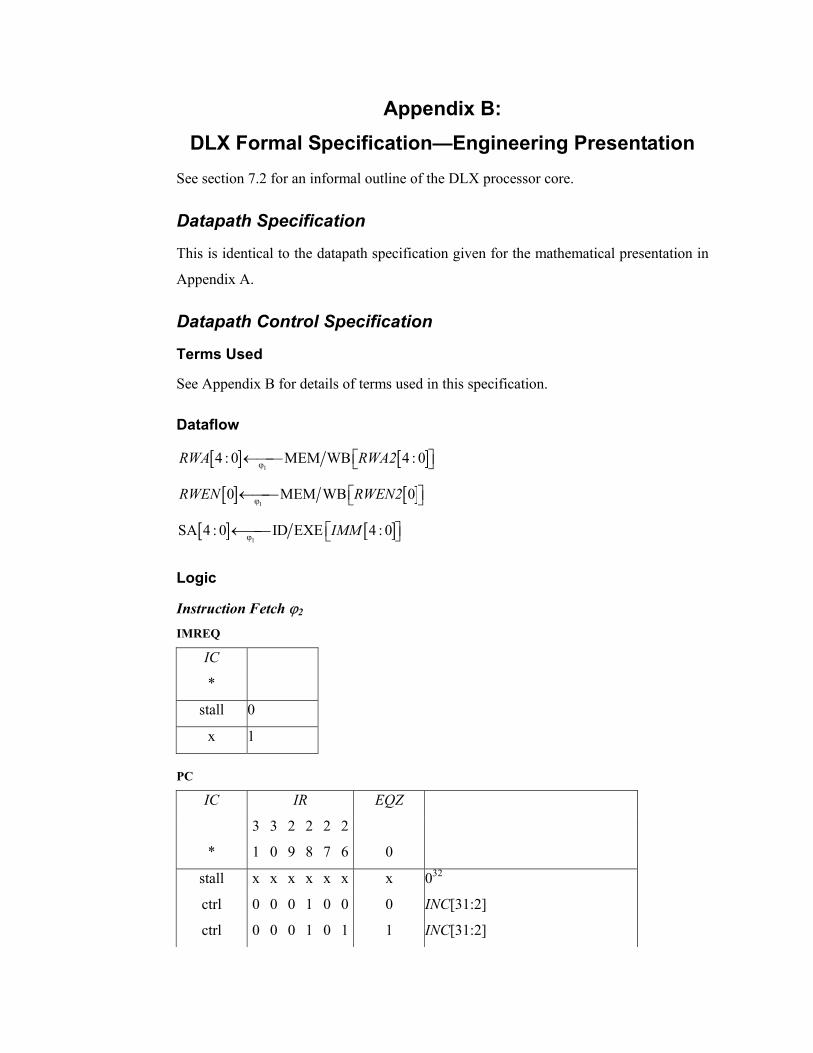
Appendix B: DLX Formal Specification—Engineering Presentation
See section 7.2 for an informal outline of the DLX processor core.
Datapath Specification
This is identical to the datapath specification given for the mathematical presentation in
Appendix A.
Datapath Control Specification
Terms Used
See Appendix B for details of terms used in this specification.
Dataflow
[ ] [ ]1
4 : 0 MEM WB 4 : 0RWA RWA2ϕ ←
[ ] [ ]1
0 MEM WB 0RWEN RWEN2ϕ ←
[ ] [ ]1
SA 4 : 0 ID EXE 4 : 0IMMϕ ←
Logic
Instruction Fetch ϕ2
IMREQ
IC
*
stall 0
x 1
PC
IC IR EQZ
*
3
1
3
0
2
9
2
8
2
7
2
6
0
stall x x x x x x x 032
ctrl 0 0 0 1 0 0 0 INC[31:2]
ctrl 0 0 0 1 0 1 1 INC[31:2]
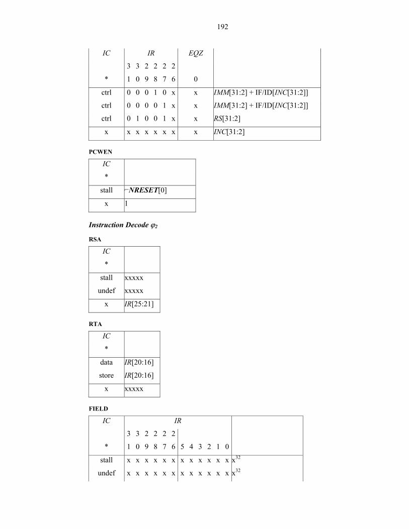
192
IC IR EQZ
*
3
1
3
0
2
9
2
8
2
7
2
6
0
ctrl 0 0 0 1 0 x x IMM[31:2] + IF/ID[INC[31:2]]
ctrl 0 0 0 0 1 x x IMM[31:2] + IF/ID[INC[31:2]]
ctrl 0 1 0 0 1 x x RS[31:2]
x x x x x x x x INC[31:2]
PCWEN
IC
*
stall ⌐NRESET[0]
x 1
Instruction Decode ϕ2
RSA
IC
*
stall xxxxx
undef xxxxx
x IR[25:21]
RTA
IC
*
data IR[20:16]
store IR[20:16]
x xxxxx
FIELD
IC IR
*
3
1
3
0
2
9
2
8
2
7
2
6
5
4
3
2
1
0
stall x x x x x x x x x x x x x32
undef x x x x x x x x x x x x x32
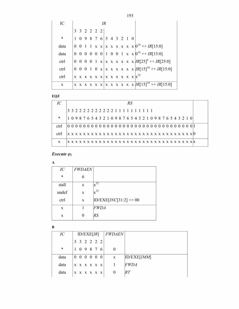
193
IC IR
*
3
1
3
0
2
9
2
8
2
7
2
6
5
4
3
2
1
0
data 0 0 1 1 x x x x x x x x 016 ++ IR[15:0]
data 0 0 0 0 0 0 1 0 0 1 x x 016 ++ IR[15:0]
ctrl 0 0 0 0 1 x x x x x x x IR[25]6 ++ IR[25:0]
ctrl 0 0 0 1 0 x x x x x x x IR[15]16 ++ IR[15:0]
ctrl x x x x x x x x x x x x x32
x x x x x x x x x x x x x IR[15]16 ++ IR[15:0]
EQZ
IC RS
*
3
1
3
0
2
9
2
8
2
7
2
6
2
5
2
4
2
3
2
2
2
1
2
0
1
9
1
8
1
7
1
6
1
5
1
4
1
3
1
2
1
1
1
0 9 8 7 6
5
4
3
2
1
0
ctrl 0 0 0 0 0 0 0 0 0 0 0 0 0 0 0 0 0 0 0 0 0 0 0 0 0 0 0 0 0 0 0 0 1
ctrl x x x x x x x x x x x x x x x x x x x x x x x x x x x x x x x x 0
x x x x x x x x x x x x x x x x x x x x x x x x x x x x x x x x x x
Execute ϕ1
A
IC FWDAEN
* 0
stall x x32
undef x x32
ctrl x ID/EXE[INC[31:2] ++ 00
x 1 FWDA
x 0 RS
B
IC ID/EXE[IR] FWDAEN
*
3
1
3
0
2
9
2
8
2
7
2
6
0
data 0 0 0 0 0 0 x ID/EXE[IMM]
data x x x x x x 1 FWDA
data x x x x x x 0 RT
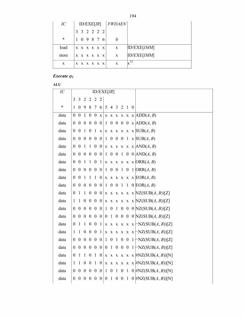
194
IC ID/EXE[IR] FWDAEN
*
3
1
3
0
2
9
2
8
2
7
2
6
0
load x x x x x x x ID/EXE[IMM]
store x x x x x x x ID/EXE[IMM]
x x x x x x x x x32
Execute ϕ2
ALU
IC ID/EXE[IR]
*
3
1
3
0
2
9
2
8
2
7
2
6
5
4
3
2
1
0
data 0 0 1 0 0 x x x x x x x ADD(A, B)
data 0 0 0 0 0 0 1 0 0 0 0 x ADD(A, B)
data 0 0 1 0 1 x x x x x x x SUB(A, B)
data 0 0 0 0 0 0 1 0 0 0 1 x SUB(A, B)
data 0 0 1 1 0 0 x x x x x x AND(A, B)
data 0 0 0 0 0 0 1 0 0 1 0 0 AND(A, B)
data 0 0 1 1 0 1 x x x x x x ORR(A, B)
data 0 0 0 0 0 0 1 0 0 1 0 1 ORR(A, B)
data 0 0 1 1 1 0 x x x x x x EOR(A, B)
data 0 0 0 0 0 0 1 0 0 1 1 0 EOR(A, B)
data 0 1 1 0 0 0 x x x x x x NZ(SUB(A, B))[Z]
data 1 1 0 0 0 0 x x x x x x NZ(SUB(A, B))[Z]
data 0 0 0 0 0 0 1 0 1 0 0 0 NZ(SUB(A, B))[Z]
data 0 0 0 0 0 0 0 1 0 0 0 0 NZ(SUB(A, B))[Z]
data 0 1 1 0 0 1 x x x x x x ⌐NZ(SUB(A, B))[Z]
data 1 1 0 0 0 1 x x x x x x ⌐NZ(SUB(A, B))[Z]
data 0 0 0 0 0 0 1 0 1 0 0 1 ⌐NZ(SUB(A, B))[Z]
data 0 0 0 0 0 0 0 1 0 0 0 1 ⌐NZ(SUB(A, B))[Z]
data 0 1 1 0 1 0 x x x x x x #NZ(SUB(A, B))[N]
data 1 1 0 0 1 0 x x x x x x #NZ(SUB(A, B))[N]
data 0 0 0 0 0 0 1 0 1 0 1 0 #NZ(SUB(A, B))[N]
data 0 0 0 0 0 0 0 1 0 0 1 0 #NZ(SUB(A, B))[N]
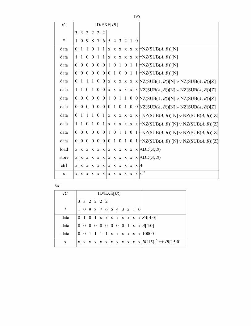
195
IC ID/EXE[IR]
*
3
1
3
0
2
9
2
8
2
7
2
6
5
4
3
2
1
0
data 0 1 1 0 1 1 x x x x x x ⌐NZ(SUB(A, B))[N]
data 1 1 0 0 1 1 x x x x x x ⌐NZ(SUB(A, B))[N]
data 0 0 0 0 0 0 1 0 1 0 1 1 ⌐NZ(SUB(A, B))[N]
data 0 0 0 0 0 0 0 1 0 0 1 1 ⌐NZ(SUB(A, B))[N]
data 0 1 1 1 0 0 x x x x x x NZ(SUB(A, B))[N] ∨ NZ(SUB(A, B))[Z]
data 1 1 0 1 0 0 x x x x x x NZ(SUB(A, B))[N] ∨ NZ(SUB(A, B))[Z]
data 0 0 0 0 0 0 1 0 1 1 0 0 NZ(SUB(A, B))[N] ∨ NZ(SUB(A, B))[Z]
data 0 0 0 0 0 0 0 1 0 1 0 0 NZ(SUB(A, B))[N] ∨ NZ(SUB(A, B))[Z]
data 0 1 1 1 0 1 x x x x x x ⌐NZ(SUB(A, B))[N] ∨ NZ(SUB(A, B))[Z]
data 1 1 0 1 0 1 x x x x x x ⌐NZ(SUB(A, B))[N] ∨ NZ(SUB(A, B))[Z]
data 0 0 0 0 0 0 1 0 1 1 0 1 ⌐NZ(SUB(A, B))[N] ∨ NZ(SUB(A, B))[Z]
data 0 0 0 0 0 0 0 1 0 1 0 1 ⌐NZ(SUB(A, B))[N] ∨ NZ(SUB(A, B))[Z]
load x x x x x x x x x x x x ADD(A, B)
store x x x x x x x x x x x x ADD(A, B)
ctrl x x x x x x x x x x x x A
x x x x x x x x x x x x x x32
SA'
IC ID/EXE[IR]
*
3
1
3
0
2
9
2
8
2
7
2
6
5
4
3
2
1
0
data 0 1 0 1 x x x x x x x x SA[4:0]
data 0 0 0 0 0 0 0 0 0 1 x x A[4:0]
data 0 0 1 1 1 1 x x x x x x 10000
x x x x x x x x x x x x x IR[15]16 ++ IR[15:0]
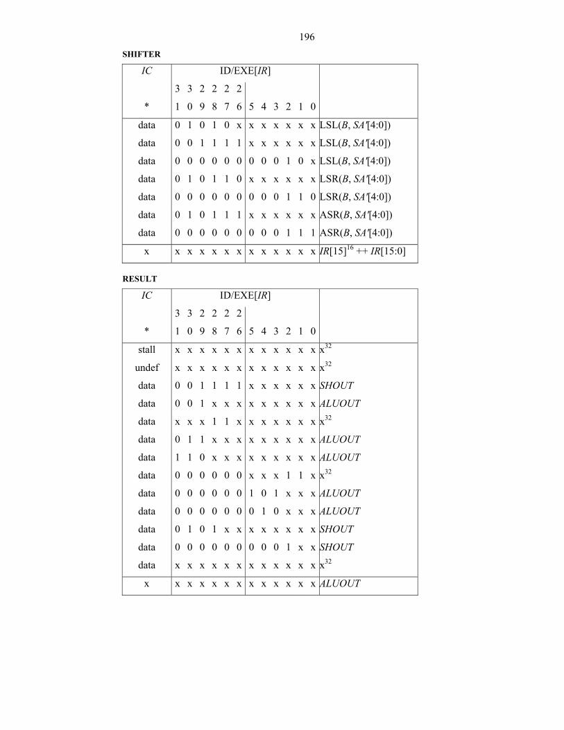
196SHIFTER
IC ID/EXE[IR]
*
3
1
3
0
2
9
2
8
2
7
2
6
5
4
3
2
1
0
data 0 1 0 1 0 x x x x x x x LSL(B, SA'[4:0])
data 0 0 1 1 1 1 x x x x x x LSL(B, SA'[4:0])
data 0 0 0 0 0 0 0 0 0 1 0 x LSL(B, SA'[4:0])
data 0 1 0 1 1 0 x x x x x x LSR(B, SA'[4:0])
data 0 0 0 0 0 0 0 0 0 1 1 0 LSR(B, SA'[4:0])
data 0 1 0 1 1 1 x x x x x x ASR(B, SA'[4:0])
data 0 0 0 0 0 0 0 0 0 1 1 1 ASR(B, SA'[4:0])
x x x x x x x x x x x x x IR[15]16 ++ IR[15:0]
RESULT
IC ID/EXE[IR]
*
3
1
3
0
2
9
2
8
2
7
2
6
5
4
3
2
1
0
stall x x x x x x x x x x x x x32
undef x x x x x x x x x x x x x32
data 0 0 1 1 1 1 x x x x x x SHOUT
data 0 0 1 x x x x x x x x x ALUOUT
data x x x 1 1 x x x x x x x x32
data 0 1 1 x x x x x x x x x ALUOUT
data 1 1 0 x x x x x x x x x ALUOUT
data 0 0 0 0 0 0 x x x 1 1 x x32
data 0 0 0 0 0 0 1 0 1 x x x ALUOUT
data 0 0 0 0 0 0 0 1 0 x x x ALUOUT
data 0 1 0 1 x x x x x x x x SHOUT
data 0 0 0 0 0 0 0 0 0 1 x x SHOUT
data x x x x x x x x x x x x x32
x x x x x x x x x x x x x ALUOUT
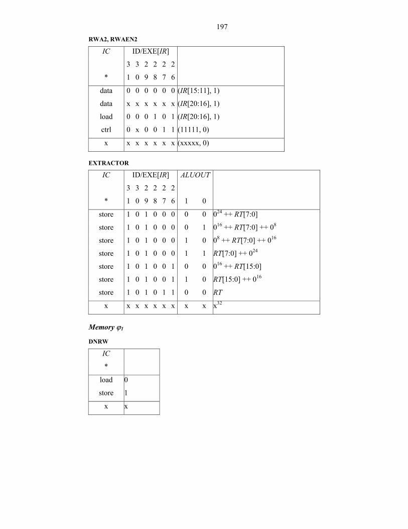
197RWA2, RWAEN2
IC ID/EXE[IR]
*
3
1
3
0
2
9
2
8
2
7
2
6
data 0 0 0 0 0 0 (IR[15:11], 1)
data x x x x x x (IR[20:16], 1)
load 0 0 0 1 0 1 (IR[20:16], 1)
ctrl 0 x 0 0 1 1 (11111, 0)
x x x x x x x (xxxxx, 0)
EXTRACTOR
IC ID/EXE[IR] ALUOUT
*
3
1
3
0
2
9
2
8
2
7
2
6
1
0
store 1 0 1 0 0 0 0 0 024 ++ RT[7:0]
store 1 0 1 0 0 0 0 1 016 ++ RT[7:0] ++ 08
store 1 0 1 0 0 0 1 0 08 ++ RT[7:0] ++ 016
store 1 0 1 0 0 0 1 1 RT[7:0] ++ 024
store 1 0 1 0 0 1 0 0 016 ++ RT[15:0]
store 1 0 1 0 0 1 1 0 RT[15:0] ++ 016
store 1 0 1 0 1 1 0 0 RT
x x x x x x x x x x32
Memory ϕ1
DNRW
IC
*
load 0
store 1
x x
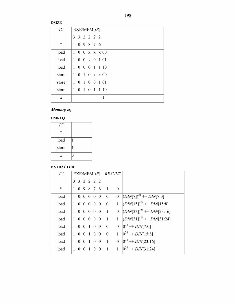
198DSIZE
IC EXE/MEM[IR]
*
3
1
3
0
2
9
2
8
2
7
2
6
load 1 0 0 x x x 00
load 1 0 0 x 0 1 01
load 1 0 0 0 1 1 10
store 1 0 1 0 x x 00
store 1 0 1 0 0 1 01
store 1 0 1 0 1 1 10
x 1
Memory ϕ2
DMREQ
IC
*
load 1
store 1
x 0
EXTRACTOR
IC EXE/MEM[IR] RESULT
*
3
1
3
0
2
9
2
8
2
7
2
6
1
0
load 1 0 0 0 0 0 0 0 (DIN[7])24 ++ DIN[7:0]
load 1 0 0 0 0 0 0 1 (DIN[15])24 ++ DIN[15:8]
load 1 0 0 0 0 0 1 0 (DIN[23])24 ++ DIN[23:16]
load 1 0 0 0 0 0 1 1 (DIN[31])24 ++ DIN[31:24]
load 1 0 0 1 0 0 0 0 024 ++ DIN[7:0]
load 1 0 0 1 0 0 0 1 024 ++ DIN[15:8]
load 1 0 0 1 0 0 1 0 024 ++ DIN[23:16]
load 1 0 0 1 0 0 1 1 024 ++ DIN[31:24]
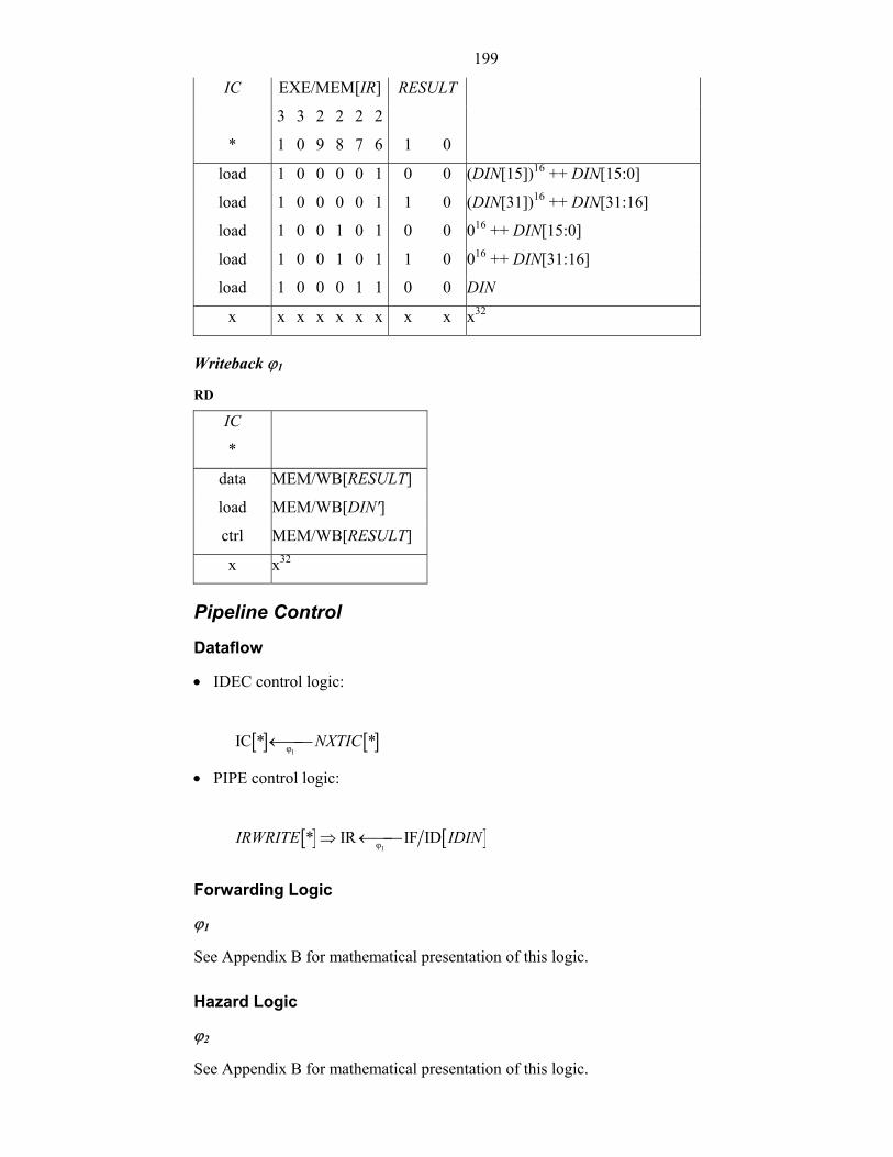
199
IC EXE/MEM[IR] RESULT
*
3
1
3
0
2
9
2
8
2
7
2
6
1
0
load 1 0 0 0 0 1 0 0 (DIN[15])16 ++ DIN[15:0]
load 1 0 0 0 0 1 1 0 (DIN[31])16 ++ DIN[31:16]
load 1 0 0 1 0 1 0 0 016 ++ DIN[15:0]
load 1 0 0 1 0 1 1 0 016 ++ DIN[31:16]
load 1 0 0 0 1 1 0 0 DIN
x x x x x x x x x x32
Writeback ϕ1
RD
IC
*
data MEM/WB[RESULT]
load MEM/WB[DIN']
ctrl MEM/WB[RESULT]
x x32
Pipeline Control
Dataflow
• IDEC control logic:
[ ] [ ]1φ
IC * *NXTIC←
• PIPE control logic:
[ ] [ ]1φ
* IR IF IDIRWRITE IDIN⇒ ←
Forwarding Logic
ϕ1
See Appendix B for mathematical presentation of this logic.
Hazard Logic
ϕ2
See Appendix B for mathematical presentation of this logic.
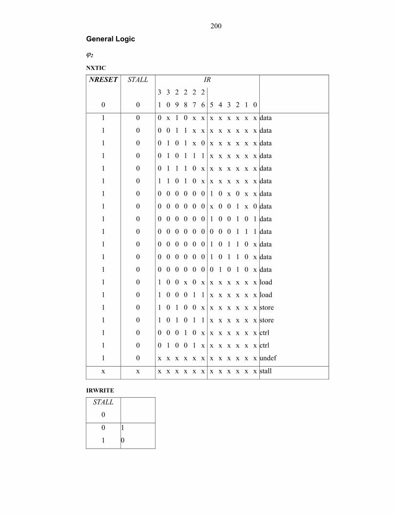
200
General Logic
ϕ2
NXTIC
NRESET STALL IR
0
0
3
1
3
0
2
9
2
8
2
7
2
6
5
4
3
2
1
0
1 0 0 x 1 0 x x x x x x x x data
1 0 0 0 1 1 x x x x x x x x data
1 0 0 1 0 1 x 0 x x x x x x data
1 0 0 1 0 1 1 1 x x x x x x data
1 0 0 1 1 1 0 x x x x x x x data
1 0 1 1 0 1 0 x x x x x x x data
1 0 0 0 0 0 0 0 1 0 x 0 x x data
1 0 0 0 0 0 0 0 x 0 0 1 x 0 data
1 0 0 0 0 0 0 0 1 0 0 1 0 1 data
1 0 0 0 0 0 0 0 0 0 0 1 1 1 data
1 0 0 0 0 0 0 0 1 0 1 1 0 x data
1 0 0 0 0 0 0 0 1 0 1 1 0 x data
1 0 0 0 0 0 0 0 0 1 0 1 0 x data
1 0 1 0 0 x 0 x x x x x x x load
1 0 1 0 0 0 1 1 x x x x x x load
1 0 1 0 1 0 0 x x x x x x x store
1 0 1 0 1 0 1 1 x x x x x x store
1 0 0 0 0 1 0 x x x x x x x ctrl
1 0 0 1 0 0 1 x x x x x x x ctrl
1 0 x x x x x x x x x x x x undef
x x x x x x x x x x x x x x stall
IRWRITE
STALL
0
0 1
1 0
201
App
endi
x C
: Gen
eral
Sim
ulat
or—
Reu
sabl
e M
odul
es in
Exe
cuta
ble
Pres
enta
tion
See
sect
ion
2.3.
3 fo
r an
expl
anat
ion
of h
ow th
e re
usab
le m
odul
es p
rese
nted
in th
is A
ppen
dix
may
be
used
to c
reat
e an
exe
cuta
ble
pres
enta
tion.
C.1
com
mon
.sm
l
This
mod
ule
cons
ists
of t
he c
omm
on d
efin
ition
s tha
t pro
vide
the
basi
s for
the
defin
ition
s of o
ther
mod
ules
.
Sum
mar
y of
Typ
es D
efin
ed b
y M
odul
e
• di
gita
l_va
lues
enu
mer
ated
type
: Rep
rese
nts
indi
vidu
al b
its u
sing
‘I’ a
nd ‘O
’, ra
ther
than
‘1’ a
nd ‘0
’ (si
nce
thes
e ar
e pr
edef
ined
to b
e of
the
int t
ype)
or b
ool (
sinc
e th
e co
ntin
ual n
eed
to re
fer t
o ‘tr
ue’ a
nd to
‘fal
se’ w
ould
pro
duce
unw
ield
y sp
ecifi
catio
ns).
• di
gita
l_va
lue
abst
ract
type
: Rep
rese
nts
parti
al w
ords
with
refe
renc
e to
a 3
2-bi
t wor
d. D
efin
ed u
sing
a 3
2-el
emen
t arr
ay to
cor
resp
ond
to 3
2-bi
t wor
d
paire
d w
ith a
32-
elem
ent v
ecto
r to
spec
ify w
hich
bits
of t
he w
ord
are
in fa
ct v
alid
.
• cl
asse
s enu
mer
ated
type
: Rep
rese
nts e
very
inst
ruct
ion
clas
s of t
he p
roce
ssor
cor
e be
ing
spec
ified
with
a u
niqu
e id
entif
ier.
• ph
ases
enu
mer
ated
type
: Rep
rese
nts e
very
clo
ck p
hase
of t
he p
roce
ssor
cor
e be
ing
spec
ified
with
a u
niqu
e id
entif
ier.
• st
ages
enu
mer
ated
type
: Rep
rese
nts e
very
pip
elin
e st
age
of th
e pr
oces
sor c
ore
bein
g sp
ecifi
ed w
ith a
uni
que
iden
tifie
r.
• st
eps
enum
erat
ed ty
pe: R
epre
sent
s ev
ery
timin
g an
nota
tion
used
to d
escr
ibe
each
of t
he in
stru
ctio
n st
eps
of th
e pr
oces
sor c
ore
bein
g sp
ecifi
ed w
ith
a un
ique
iden
tifie
r.
• *_
phys
ical
_reg
s en
umer
ated
typ
e: F
or e
ach
bank
of
phys
ical
reg
iste
rs r
equi
red
by t
he p
roce
ssor
cor
e be
ing
spec
ified
, rep
rese
nts
ever
y ph
ysic
al
regi
ster
in th
at b
ank
with
a u
niqu
e id
entif
ier.
(Eac
h ba
nk o
f phy
sica
l reg
iste
rs sh
ould
be
asso
ciat
ed w
ith it
s ow
n *_
phys
ical
_reg
s enu
mer
ated
type
.)
202
• *_
virt
ual_
regs
uni
on ty
pe: F
or e
ach
bank
of p
hysi
cal r
egis
ters
requ
ired
by th
e pr
oces
sor c
ore
bein
g sp
ecifi
ed, a
tupl
e of
the
optio
nal t
ypes
requ
ired
to r
epre
sent
eac
h ph
ysic
al r
egis
ter
as a
virt
ual r
egis
ter
at th
e Pr
ogra
mm
er’s
Mod
el le
vel o
f abs
tract
ion.
(Eac
h ba
nk o
f phy
sica
l reg
iste
rs s
houl
d be
asso
ciat
ed w
ith it
s ow
n *_
virt
ual_
regs
enu
mer
ated
type
.)
Stan
dard
ML
Impl
emen
tatio
n of
Mod
ule
exception Error of string;
fun error error = raise Error(error)
nonfix guard;
fun guard (SOME option, _ ) = option
| guard (NONE , error) = raise Error(error);
infix guard;
nonfix guardf;
fun guardf (x, (f, error)) = (f x) guard error;
infix guardf;
datatype classes = (* See Summary of Types Defined by Module above *)
val classes_to_string : classes -> string =
(* function that maps each constructor of the classes data type to a string to facilitate production of debug output *)
datatype steps = (* See Summary of Types Defined by Module above *)
val steps_to_string : steps -> string =
(* function that maps each constructor of the steps data type to a string to facilitate production of debug output. *)
datatype phases = (* See Summary of Types Defined by Module above *)
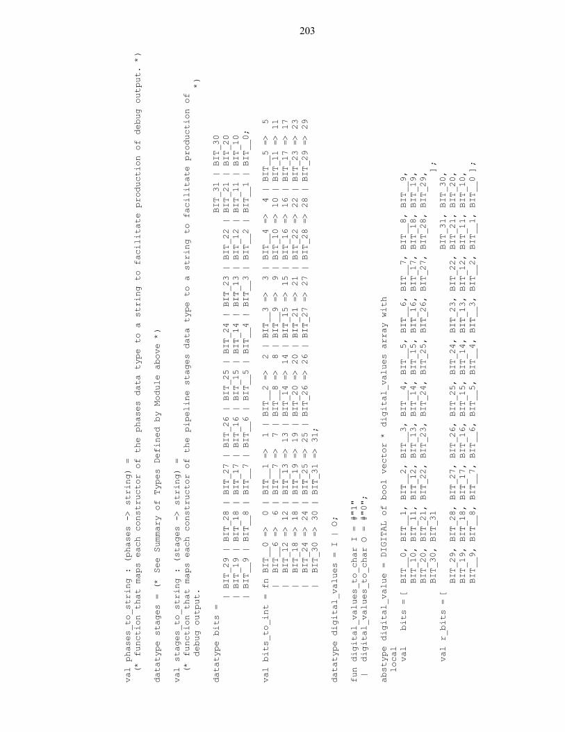
203
val phases_to_string : (phases -> string) =
(* function that maps each constructor of the phases data type to a string to facilitate production of debug output. *)
datatype stages = (* See Summary of Types Defined by Module above *)
val stages_to_string : (stages -> string) =
(* function that maps each constructor of the pipeline stages data type to a string to facilitate production of
debug output. *)
datatype bits = BIT_31 | BIT_30
| BIT_29 | BIT_28 | BIT_27 | BIT_26 | BIT_25 | BIT_24 | BIT_23 | BIT_22 | BIT_21 | BIT_20
| BIT_19 | BIT_18 | BIT_17 | BIT_16 | BIT_15 | BIT_14 | BIT_13 | BIT_12 | BIT_11 | BIT_10
| BIT__9 | BIT__8 | BIT__7 | BIT__6 | BIT__5 | BIT__4 | BIT__3 | BIT__2 | BIT__1 | BIT__0;
val bits_to_int = fn BIT__0 => 0 | BIT__1 => 1 | BIT__2 => 2 | BIT__3 => 3 | BIT__4 => 4 | BIT__5 => 5
| BIT__6 => 6 | BIT__7 => 7 | BIT__8 => 8 | BIT__9 => 9 | BIT_10 => 10 | BIT_11 => 11
| BIT_12 => 12 | BIT_13 => 13 | BIT_14 => 14 | BIT_15 => 15 | BIT_16 => 16 | BIT_17 => 17
| BIT_18 => 18 | BIT_19 => 19 | BIT_20 => 20 | BIT_21 => 21 | BIT_22 => 22 | BIT_23 => 23
| BIT_24 => 24 | BIT_25 => 25 | BIT_26 => 26 | BIT_27 => 27 | BIT_28 => 28 | BIT_29 => 29
| BIT_30 => 30 | BIT_31 => 31;
datatype digital_values = I | O;
fun digital_values_to_char I = #"1"
| digital_values_to_char O = #"0";
abstype digital_value = DIGITAL of bool vector * digital_values array with
local
val bits = [ BIT__0, BIT__1, BIT__2, BIT__3, BIT__4, BIT__5, BIT__6, BIT__7, BIT__8, BIT__9,
BIT_10, BIT_11, BIT_12, BIT_13, BIT_14, BIT_15, BIT_16, BIT_17, BIT_18, BIT_19,
BIT_20, BIT_21, BIT_22, BIT_23, BIT_24, BIT_25, BIT_26, BIT_27, BIT_28, BIT_29,
BIT_30, BIT_31 ];
val r_bits = [ BIT_31, BIT_30,
BIT_29, BIT_28, BIT_27, BIT_26, BIT_25, BIT_24, BIT_23, BIT_22, BIT_21, BIT_20,
BIT_19, BIT_18, BIT_17, BIT_16, BIT_15, BIT_14, BIT_13, BIT_12, BIT_11, BIT_10,
BIT__9, BIT__8, BIT__7, BIT__6, BIT__5, BIT__4, BIT__3, BIT__2, BIT__1, BIT__0 ];
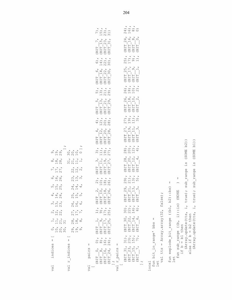
204
val indices = [ 0, 1, 2, 3, 4, 5, 6, 7, 8, 9,
10, 11, 12, 13, 14, 15, 16, 17, 18, 19,
20, 21, 22, 23, 24, 25, 26, 27, 28, 29,
30, 31 ];
val r_indices = [ 31, 30,
29, 28, 27, 26, 25, 24, 23, 22, 21, 20,
19, 18, 17, 16, 15, 14, 13, 12, 11, 10,
9, 8, 7, 6, 5, 4, 3, 2, 1, 0 ];
val pairs =
[
(BIT__0, 0), (BIT__1, 1), (BIT__2, 2), (BIT__3, 3), (BIT__4, 4), (BIT__5, 5), (BIT__6, 6), (BIT__7, 7),
(BIT__8, 8), (BIT__9, 9), (BIT_10, 10), (BIT_11, 11), (BIT_12, 12), (BIT_13, 13), (BIT_14, 14), (BIT_15, 15),
(BIT_16, 16), (BIT_17, 17), (BIT_18, 18), (BIT_19, 19), (BIT_20, 20), (BIT_21, 21), (BIT_22, 22), (BIT_23, 23),
(BIT_24, 24), (BIT_25, 25), (BIT_26, 26), (BIT_27, 27), (BIT_28, 28), (BIT_29, 29), (BIT_30, 30), (BIT_31, 31)
];
val r_pairs =
[
(BIT_31, 31), (BIT_30, 30), (BIT_29, 29), (BIT_28, 28), (BIT_27, 27), (BIT_26, 26), (BIT_25, 25), (BIT_24, 24),
(BIT_23, 23), (BIT_22, 22), (BIT_21, 21), (BIT_20, 20), (BIT_19, 19), (BIT_18, 18), (BIT_17, 17), (BIT_16, 16),
(BIT_15, 15), (BIT_14, 14), (BIT_13, 13), (BIT_12, 12), (BIT_11, 11), (BIT_10, 10), (BIT__9, 9), (BIT__8, 8),
(BIT__7, 7), (BIT__6, 6), (BIT__5, 5), (BIT__4, 4), (BIT__3, 3), (BIT__2, 2), (BIT__1, 1), (BIT__0, 0)
];
local
fun bit_in_range' bbs =
let
val tts = Array.array(32, false);
fun explode_bit_range ((b1, b2)::bs) =
let
fun sub_range ((b, i)::is) (NONE ) =
if b = b1 then
(Array.update(tts, i, true); sub_range is (SOME b2))
else if b = b2 then
(Array.update(tts, i, true); sub_range is (SOME b1))
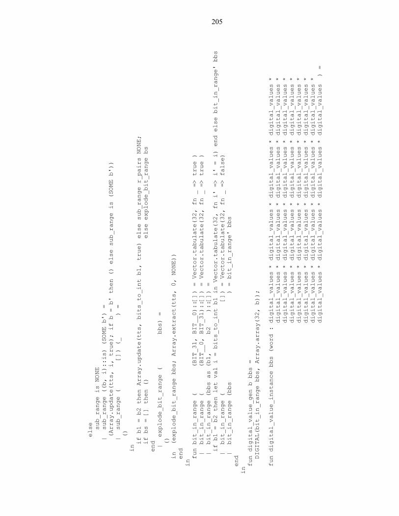
205
else
sub_range is NONE
| sub_range ((b, i)::is) (SOME b') =
(Array.update(tts, i, true); if b = b' then () else sub_range is (SOME b'))
| sub_range ( []) (_ ) =
()
in
if b1 = b2 then Array.update(tts, bits_to_int b1, true) else sub_range r_pairs NONE;
if bs = [] then () else explode_bit_range bs
end
| explode_bit_range ( bbs) =
()
in (explode_bit_range bbs; Array.extract(tts, 0, NONE))
end
in
fun bit_in_range ( (BIT_31, BIT__0)::[]) = Vector.tabulate(32, fn _ => true )
| bit_in_range ( (BIT__0, BIT_31)::[]) = Vector.tabulate(32, fn _ => true )
| bit_in_range (bbs as (b1, b2 )::[]) =
if b1 = b2 then let val i = bits_to_int b1 in Vector.tabulate(32, fn i' => i' = i) end else bit_in_range' bbs
| bit_in_range ( []) = Vector.tabulate(32, fn _ => false)
| bit_in_range (bbs ) = bit_in_range' bbs
end
in
fun digital_value_gen b bbs =
DIGITAL(bit_in_range bbs, Array.array(32, b));
fun digital_value_instance bbs (word : digital_values * digital_values * digital_values * digital_values *
digital_values * digital_values * digital_values * digital_values *
digital_values * digital_values * digital_values * digital_values *
digital_values * digital_values * digital_values * digital_values *
digital_values * digital_values * digital_values * digital_values *
digital_values * digital_values * digital_values * digital_values *
digital_values * digital_values * digital_values * digital_values *
digital_values * digital_values * digital_values * digital_values ) =
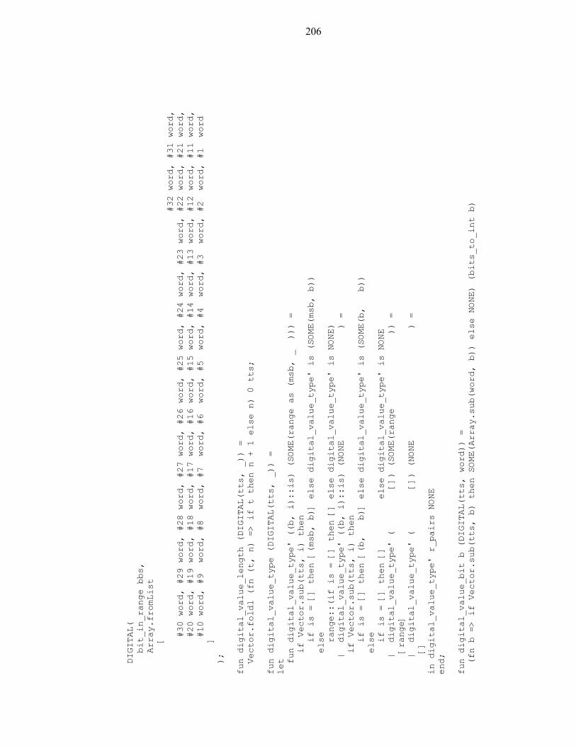
206
DIGITAL(
bit_in_range bbs,
Array.fromList
[
#32 word, #31 word,
#30 word, #29 word, #28 word, #27 word, #26 word, #25 word, #24 word, #23 word, #22 word, #21 word,
#20 word, #19 word, #18 word, #17 word, #16 word, #15 word, #14 word, #13 word, #12 word, #11 word,
#10 word, #9 word, #8 word, #7 word, #6 word, #5 word, #4 word, #3 word, #2 word, #1 word
]
);
fun digital_value_length (DIGITAL(tts, _)) =
Vector.foldl (fn (t, n) => if t then n + 1 else n) 0 tts;
fun digital_value_type (DIGITAL(tts, _)) =
let
fun digital_value_type' ((b, i)::is) (SOME(range as (msb, _ ))) =
if Vector.sub(tts, i) then
if is = [] then [(msb, b)] else digital_value_type' is (SOME(msb, b))
else
range::(if is = [] then [] else digital_value_type' is NONE)
| digital_value_type' ((b, i)::is) (NONE ) =
if Vector.sub(tts, i) then
if is = [] then [(b, b)] else digital_value_type' is (SOME(b, b))
else
if is = [] then [] else digital_value_type' is NONE
| digital_value_type' ( []) (SOME(range )) =
[range]
| digital_value_type' ( []) (NONE ) =
[]
in digital_value_type' r_pairs NONE
end;
fun digital_value_bit b (DIGITAL(tts, word)) =
(fn b => if Vector.sub(tts, b) then SOME(Array.sub(word, b)) else NONE) (bits_to_int b)
207
fun digital_value_eval (DIGITAL(tts, word)) =
let
fun digital_value_eval' (i::is) option =
let
val option' =
case option
of SOME n => SOME(n + n + (if Vector.sub(tts, i) andalso Array.sub(word, i) = I then 1 else 0))
| NONE => if Vector.sub(tts, i) then SOME(if Array.sub(word, i) = I then 1 else 0) else NONE
in if is = [] then option' else digital_value_eval' is option'
end
| digital_value_eval' ( []) option =
option
in digital_value_eval' r_indices NONE
end;
fun digital_value_compare (DIGITAL(tts', word'), DIGITAL(tts, word)) =
let
fun digital_value_compare' (i::is) result = (
case (Vector.sub(tts', i), Vector.sub(tts, i)) of (false, false) =>
if is = [] then result else digital_value_compare' is result
| (true, true ) =>
let
val result' = case (Array.sub(word', i), Array.sub(word, i)) of (I, O) => SOME GREATER
| (O, I) => SOME LESS
| (_, _) => result
in if is = [] then result' else digital_value_compare' is result'
end
| (_, _ ) =>
NONE
)
| digital_value_compare' ( []) result =
result
in digital_value_compare' indices (SOME EQUAL)
end
fun digital_value_equal_type bbs (DIGITAL(tts, _)) = (bit_in_range bbs) = tts;
208
fun digital_value_sign (DIGITAL(tts, word)) =
let
fun digital_value_sign' (i::is) =
if Vector.sub(tts, i) then SOME(Array.sub(word, i)) else if is = [] then NONE else digital_value_sign' is
| digital_value_sign' ( []) =
NONE
in digital_value_sign' r_indices
end;
fun digital_value_zero (DIGITAL(tts, word)) =
let
fun digital_value_zero' (i::is) option =
if Vector.sub(tts, i) then
if Array.sub(word, i) = I then
SOME false
else
if is = [] then SOME true else digital_value_zero' is (SOME true)
else
if is = [] then option else digital_value_zero' is option
| digital_value_zero' ( []) option =
option
in digital_value_zero' indices NONE
end;
fun digital_value_bit_set b (digital_value as DIGITAL(tts, word)) bit =
let
val i = bits_to_int b
in
if Vector.sub(tts, i) then
let
val word' = Array.tabulate(32, fn i => Array.sub(word, i))
in
Array.update(word', i, bit); SOME(DIGITAL(tts, word'))
end
else
NONE
end;
209
local
fun digital_value_extend bit bbs (DIGITAL(tts, word)) =
let
datatype extend_state = UNSTARTED | KEEP_OLD | EXTEND_NEW | FINISHED;
val tts' = bit_in_range bbs;
fun digital_value_extend' (i::is) state = (
case (Vector.sub(tts', i), Vector.sub(tts, i)) of (false, false) =>
if is = [] then true else digital_value_extend' is (if state = EXTEND_NEW then FINISHED else state)
| (true, true ) =>
if state = KEEP_OLD orelse state = UNSTARTED then
if is = [] then true else digital_value_extend' is KEEP_OLD
else
false
| (true, false) =>
if state = EXTEND_NEW orelse state = KEEP_OLD then
if is = [] then true else digital_value_extend' is EXTEND_NEW
else
false
| (false, true ) =>
false
)
| digital_value_extend' ( []) state =
true
in
if digital_value_extend' indices UNSTARTED then
SOME(DIGITAL(tts', Array.tabulate(32, fn i => if Vector.sub(tts, i) orelse not(Vector.sub(tts', i)) then
Array.sub(word, i) else bit)))
else
NONE
end
in
fun digital_value_sign_extend bbs digital_value =
case (digital_value_sign digital_value) of SOME sign => digital_value_extend sign bbs digital_value
| NONE => NONE
210
val digital_value_zero_extend = digital_value_extend O
end;
fun digital_value_pad bit bbs (DIGITAL(tts, word)) =
let
val tts' = bit_in_range bbs;
fun digital_value_pad' (i::is) =
if Vector.sub(tts, i) andalso not(Vector.sub(tts', i)) then
false
else
if is = [] then true else digital_value_pad' is
| digital_value_pad' ( []) =
true
in
if digital_value_pad' indices then
SOME(DIGITAL(tts', Array.tabulate(32, fn i => if Vector.sub(tts, i) orelse not(Vector.sub(tts', i)) then
Array.sub(word, i) else bit)))
else
NONE
end;
fun digital_value_concatenate (DIGITAL(tts', word'), DIGITAL(tts, word)) =
let
datatype concatenate_state = UNSTARTED | STARTED' | STARTED | FINISHED' | FINISHED;
fun digital_value_concatenate' (i::is) state = (
case (Vector.sub(tts', i), Vector.sub(tts, i)) of (false, false) =>
if is = [] then true else digital_value_concatenate' is state
| (true, false) =>
if state = STARTED' orelse state = UNSTARTED then
digital_value_concatenate' is STARTED'
else
if state = FINISHED' then false else if is = [] then true else digital_value_concatenate' is FINISHED
| (false, true ) =>
if state = STARTED orelse state = UNSTARTED then
digital_value_concatenate' is STARTED
211
else
if state = FINISHED then false else if is = [] then true else digital_value_concatenate' is FINISHED'
| (true, true ) =>
false
)
| digital_value_concatenate' ( []) state =
true
in
if digital_value_concatenate' indices UNSTARTED then
SOME(DIGITAL(Vector.tabulate(32, fn i => Vector.sub(tts', i) orelse Vector.sub(tts, i)),
Array.tabulate(32, fn i => Array.sub(if Vector.sub(tts, i) then word else word', i))))
else
NONE
end;
fun digital_value_replace (DIGITAL(tts', word'), DIGITAL(tts, word)) =
let
fun digital_value_replace' (i::is) =
if Vector.sub(tts, i) andalso not(Vector.sub(tts', i)) then
false
else
if is = [] then true else digital_value_replace' is
| digital_value_replace' ( []) =
true
in
if digital_value_replace' indices then
SOME(DIGITAL(tts', Array.tabulate(32, fn i => Array.sub(if Vector.sub(tts, i) then word else word', i))))
else
NONE
end;
fun digital_value_slice bbs (DIGITAL(tts, word)) =
let
val tts' = bit_in_range bbs;
212
fun digital_value_slice' (i::is) =
if Vector.sub(tts', i) andalso not(Vector.sub(tts, i)) then
false
else
if is = [] then true else digital_value_slice' is
| digital_value_slice' ( []) =
true
in
if digital_value_slice' indices then SOME(DIGITAL(tts', Array.tabulate(32, fn i => Array.sub(word, i)))) else NONE
end;
fun digital_value_splice (DIGITAL(tts', word'), DIGITAL(tts, word)) =
let
fun digital_value_splice' (i::is) =
if Vector.sub(tts', i) andalso Vector.sub(tts, i) then
false
else
if is = [] then true else digital_value_splice' is
| digital_value_splice' ( []) =
true
in
if digital_value_splice' indices then
SOME(DIGITAL(Vector.tabulate(32, fn i => Vector.sub(tts', i) orelse Vector.sub(tts, i)), Array.tabulate(32,
fn i => Array.sub(if Vector.sub(tts, i) then word else word', i))))
else
NONE
end;
fun digital_value_map f (DIGITAL(tts, word)) =
DIGITAL(tts, Array.tabulate(32, fn i => if Vector.sub(tts, i) then f (Array.sub(word, i)) else Array.sub(word,
i)));
fun digital_value_dyadic f (DIGITAL(tts', word'), DIGITAL(tts, word)) =
let
fun digital_value_dyadic' (i::is) =
if Vector.sub(tts', i) <> Vector.sub(tts, i) then
false
213
else
if is = [] then true else digital_value_dyadic' is
| digital_value_dyadic' ( []) =
true
in
if digital_value_dyadic' indices then
SOME(DIGITAL(tts', Array.tabulate(32, fn i => if Vector.sub(tts', i) then f (Array.sub(word', i), Array.sub(word,
i)) else Array.sub(word', i))))
else
NONE
end;
local
fun not' x = if x = O then I else O;
fun and' (x, y) = if x = I andalso y = I then I else O;
fun or' (x, y) = if x = O andalso y = O then O else I;
fun xor' (x, y) = if x <> y then I else O;
fun add' (DIGITAL(tts', word'), DIGITAL(tts, word)) c =
let
val result = Array.array(32, O);
fun add'' (i::is) c = (
case (Vector.sub(tts', i), Vector.sub(tts, i)) of (false, false) =>
if is = [] then true else add'' is c
| (true, true ) =>
let
val c' =
if Array.sub(word', i) = Array.sub(word, i) then
(if c = I then Array.update(result, i, I) else (); Array.sub(word', i))
else
(if c = O then Array.update(result, i, I) else (); c)
in if is = [] then true else add'' is c'
end
214
| (_, _ ) =>
false
)
| add'' ( []) c =
true
in if add'' indices c then SOME(DIGITAL(tts', result)) else NONE
end
in
fun digital_value_add (x, y) c = add' (x, y ) c;
fun digital_value_sub (x, y) c = add' (x, (digital_value_not y)) c;
fun digital_value_not x = digital_value_map (not') x;
fun digital_value_and (x, y) = digital_value_dyadic (and') (x, y);
fun digital_value_or (x, y) = digital_value_dyadic (or' ) (x, y);
fun digital_value_xor (x, y) = digital_value_dyadic (xor') (x, y)
end;
local
datatype operation = DROP | RDROP | RTAKE | TAKE;
fun operate (n, tts) operation =
let
val (bound, compare) = case operation of DROP => (32, op>=)
| RDROP => (~1, op<=)
| RTAKE => (~1, op> )
| TAKE => (32, op< );
fun operate' n (i::is) =
if n <= 0 then i else if is = [] then bound else operate' (if Vector.sub(tts, i) then n - 1 else n) is
| operate' n ( []) =
bound;
val n' = operate' n (if operation = DROP orelse operation = TAKE then indices else r_indices)
in Vector.tabulate(32, fn i => compare(i, n') andalso Vector.sub(tts, i))
end;
215
fun digital_value_copy (tts', word') (tts, word) indices =
let
fun digital_value_copy' (jjs as j::js) (iis as i::is) = (
case (Vector.sub(tts', j), Vector.sub(tts, i)) of (true, true ) => (
Array.update(word', j, Array.sub(word, i));
if js = [] orelse is = [] then word' else digital_value_copy' js is
)
| (false, true ) =>
if js = [] then word' else digital_value_copy' js iis
| (_, false) =>
if is = [] then word' else digital_value_copy' jjs is
)
| digital_value_copy' ( _) ( _) =
word'
in digital_value_copy' indices indices
end
in
fun digital_value_drop (DIGITAL(tts, word), n) = DIGITAL(operate (n, tts) DROP, word);
fun digital_value_rdrop (DIGITAL(tts, word), n) = DIGITAL(operate (n, tts) RDROP, word);
fun digital_value_take (DIGITAL(tts, word), n) = DIGITAL(operate (n, tts) TAKE, word);
fun digital_value_rtake (DIGITAL(tts, word), n) = DIGITAL(operate (n, tts) RTAKE, word);
fun digital_value_asr (immediate as DIGITAL(tts, word), shift_amnt) =
let
val sign = getOpt(digital_value_sign immediate, O));
val (tts', word') = (operate (getOpt(digital_value_eval shift_amnt, 0), tts) DROP, Array.array(32, sign))
in DIGITAL(tts, digital_value_copy (tts, word') (tts', word) indices)
end;
fun digital_value_lsl ( DIGITAL(tts, word), shift_amnt) =
let
val (tts', word') = (operate (getOpt(digital_value_eval shift_amnt, 0), tts) RDROP, Array.array(32, O ))
in DIGITAL(tts, digital_value_copy (tts, word') (tts', word) r_indices)
end;
fun digital_value_lsr ( DIGITAL(tts, word), shift_amnt) =
let
val (tts', word') = (operate (getOpt(digital_value_eval shift_amnt, 0), tts) DROP, Array.array(32, O ))
216
in DIGITAL(tts, digital_value_copy (tts, word') (tts', word) indices)
end;
fun digital_value_rol (immediate as DIGITAL(tts, word), rot_amnt ) =
case (digital_value_length immediate) of 0 =>
immediate
| length =>
let
val rot_amnt' = (getOpt(digital_value_eval rot_amnt, 0)) mod length;
val front_tts = operate (rot_amnt', tts) RTAKE;
val back_tts = operate (rot_amnt', tts) RDROP;
in DIGITAL(tts, digital_value_copy (tts, digital_value_copy (tts, Array.tabulate(32, fn i => Array.sub(word, i)))
(front_tts, word) indices) (back_tts, word) r_indices)
end;
fun digital_value_ror (immediate as DIGITAL(tts, word), rot_amnt ) =
case (digital_value_length immediate) of 0 =>
immediate
| length =>
let
val rot_amnt' = (getOpt(digital_value_eval rot_amnt, 0)) mod length;
val front_tts = operate (rot_amnt', tts) DROP;
val back_tts = operate (rot_amnt', tts) TAKE
in DIGITAL(tts, digital_value_copy (tts, digital_value_copy (tts, Array.tabulate(32, fn i => Array.sub(word, i)))
(front_tts, word) indices) (back_tts, word) r_indices)
end
end;
fun digital_value_replicate bbs (DIGITAL(tts, word)) =
let
val replicate = Vector.foldri (fn (i, true, is) => i::is | (_, false, is) => is) [] (tts, 0, NONE);
val (tts', word') = (bit_in_range bbs, Array.array(32, O));
217
fun digital_value_replicate' ( j::js) (iis as i::is) = (
case Vector.sub(tts', j) of true =>
let val _ = Array.update(word', j, Array.sub(word, i))
in if js = [] then is = [] else digital_value_replicate' js is
end
| false =>
if js = [] then false else digital_value_replicate' js iis
)
| digital_value_replicate' (jjs as j::js) ( []) =
if Vector.sub(tts', j) then
digital_value_replicate' jjs replicate
else
if js = [] then true else digital_value_replicate' js []
| digital_value_replicate' ( _) ( _) =
true
in if replicate <> [] andalso digital_value_replicate' indices replicate then SOME(DIGITAL(tts', word')) else NONE
end
fun digital_value_foldl f e (DIGITAL(tts, word)) =
Array.foldli (fn (i, a, e') => if Vector.sub(tts, i) then f (a, e') else e') e (word, 0, NONE);
fun digital_value_foldr f e (DIGITAL(tts, word)) =
Array.foldri (fn (i, a, e') => if Vector.sub(tts, i) then f (a, e') else e') e (word, 0, NONE);
local
fun digital_value_foldi fold f e (DIGITAL(tts, word), i, iend) =
let
fun slice_pairs (iis' as ( (b, i''))::is') ( NONE) =
if b <> i then
slice_pairs is' NONE
else (
case (iend) of NONE => slice_pairs iis' (SOME 0)
| SOME n => if n <= 0 then [] else slice_pairs iis' (SOME n)
)
| slice_pairs ( (i as (_, i''))::is') (SOME n) =
if Vector.sub(tts, i'') then
if n = 1 then [i] else i::slice_pairs is' (SOME(n - 1))
218
else
slice_pairs is' (SOME n)
| slice_pairs ( []) ( _) =
[];
val pairs = slice_pairs pairs NONE
in
if case iend of NONE => true | SOME n => length pairs = n then
SOME(fold (fn ((b, i), e') => f (b, Array.sub(word, i), e')) e pairs)
else
NONE
end
in
fun digital_value_foldli f e slice = digital_value_foldi foldl f e slice;
fun digital_value_foldri f e slice = digital_value_foldi foldr f e slice
end
local
val zero = DIGITAL(Vector.tabulate(32, fn i => i <= 5), Array.array(32, O))
in
val digital_value_count_ones = digital_value_foldl (fn (x, y) => if x = O then y else (digital_value_add (y, zero)
I) guard "digital_value_add unexpectedly returned NONE in digital_value_count_ones") (zero)
end;
fun digital_value_from_int bbs int =
let
val (tts, word) = (bit_in_range bbs, Array.array(32, O));
fun digital_value_from_int' (i::is) int =
let
val (div_by_2, mod_by_2) = (int div 2, int mod 2);
in
case (Vector.sub(tts, i)) of true => (
Array.update(word, i, if mod_by_2 = 1 then I else O);
if is = [] then div_by_2 = 0 else digital_value_from_int' is div_by_2
)
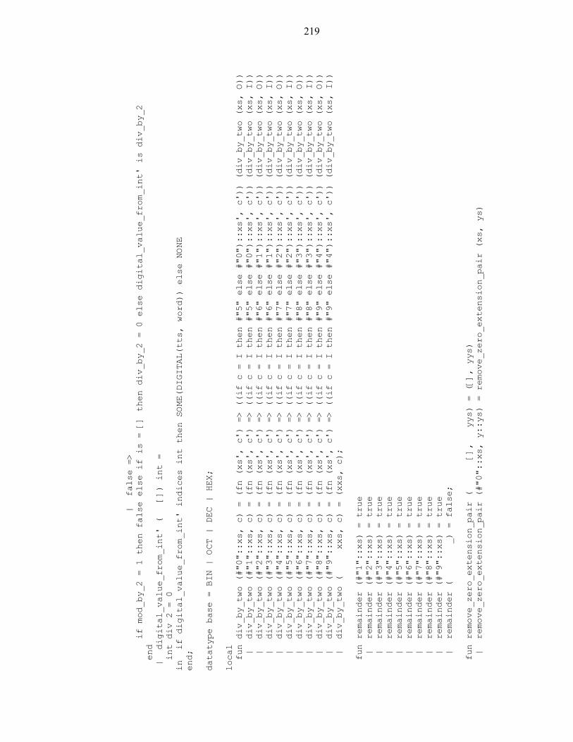
219
| false =>
if mod_by_2 = 1 then false else if is = [] then div_by_2 = 0 else digital_value_from_int' is div_by_2
end
| digital_value_from_int' ( []) int =
int div 2 = 0
in if digital_value_from_int' indices int then SOME(DIGITAL(tts, word)) else NONE
end;
datatype base = BIN | OCT | DEC | HEX;
local
fun div_by_two (#"0"::xs, c) = (fn (xs', c') => ((if c = I then #"5" else #"0")::xs', c')) (div_by_two (xs, O))
| div_by_two (#"1"::xs, c) = (fn (xs', c') => ((if c = I then #"5" else #"0")::xs', c')) (div_by_two (xs, I))
| div_by_two (#"2"::xs, c) = (fn (xs', c') => ((if c = I then #"6" else #"1")::xs', c')) (div_by_two (xs, O))
| div_by_two (#"3"::xs, c) = (fn (xs', c') => ((if c = I then #"6" else #"1")::xs', c')) (div_by_two (xs, I))
| div_by_two (#"4"::xs, c) = (fn (xs', c') => ((if c = I then #"7" else #"2")::xs', c')) (div_by_two (xs, O))
| div_by_two (#"5"::xs, c) = (fn (xs', c') => ((if c = I then #"7" else #"2")::xs', c')) (div_by_two (xs, I))
| div_by_two (#"6"::xs, c) = (fn (xs', c') => ((if c = I then #"8" else #"3")::xs', c')) (div_by_two (xs, O))
| div_by_two (#"7"::xs, c) = (fn (xs', c') => ((if c = I then #"8" else #"3")::xs', c')) (div_by_two (xs, I))
| div_by_two (#"8"::xs, c) = (fn (xs', c') => ((if c = I then #"9" else #"4")::xs', c')) (div_by_two (xs, O))
| div_by_two (#"9"::xs, c) = (fn (xs', c') => ((if c = I then #"9" else #"4")::xs', c')) (div_by_two (xs, I))
| div_by_two ( xxs, c) = (xxs, c);
fun remainder (#"1"::xs) = true
| remainder (#"2"::xs) = true
| remainder (#"3"::xs) = true
| remainder (#"4"::xs) = true
| remainder (#"5"::xs) = true
| remainder (#"6"::xs) = true
| remainder (#"7"::xs) = true
| remainder (#"8"::xs) = true
| remainder (#"9"::xs) = true
| remainder ( _) = false;
fun remove_zero_extension_pair ( [], yys) = ([], yys)
| remove_zero_extension_pair (#"0"::xs, y::ys) = remove_zero_extension_pair (xs, ys)
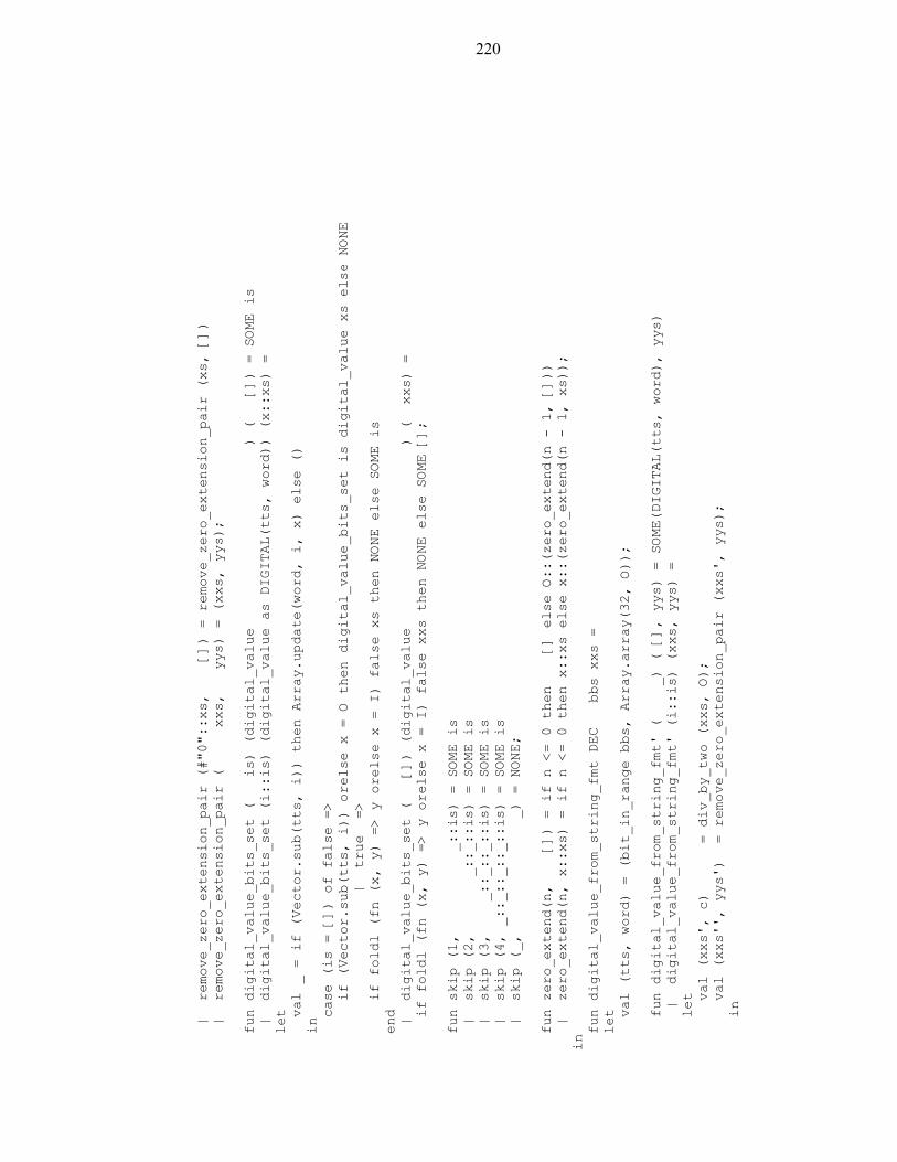
220
| remove_zero_extension_pair (#"0"::xs, []) = remove_zero_extension_pair (xs, [])
| remove_zero_extension_pair ( xxs, yys) = (xxs, yys);
fun digital_value_bits_set ( is) (digital_value ) ( []) = SOME is
| digital_value_bits_set (i::is) (digital_value as DIGITAL(tts, word)) (x::xs) =
let
val _ = if (Vector.sub(tts, i)) then Array.update(word, i, x) else ()
in
case (is = []) of false =>
if (Vector.sub(tts, i)) orelse x = O then digital_value_bits_set is digital_value xs else NONE
| true =>
if foldl (fn (x, y) => y orelse x = I) false xs then NONE else SOME is
end
| digital_value_bits_set ( []) (digital_value ) ( xxs) =
if foldl (fn (x, y) => y orelse x = I) false xxs then NONE else SOME [];
fun skip (1, _::is) = SOME is
| skip (2, _::_::is) = SOME is
| skip (3, _::_::_::is) = SOME is
| skip (4, _::_::_::_::is) = SOME is
| skip (_, _) = NONE;
fun zero_extend(n, []) = if n <= 0 then [] else O::(zero_extend(n - 1, []))
| zero_extend(n, x::xs) = if n <= 0 then x::xs else x::(zero_extend(n - 1, xs));
in
fun digital_value_from_string_fmt DEC bbs xxs =
let
val (tts, word) = (bit_in_range bbs, Array.array(32, O));
fun digital_value_from_string_fmt' ( _) ( [], yys) = SOME(DIGITAL(tts, word), yys)
| digital_value_from_string_fmt' (i::is) (xxs, yys) =
let
val (xxs', c) = div_by_two (xxs, O);
val (xxs'', yys') = remove_zero_extension_pair (xxs', yys);
in
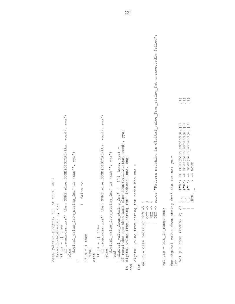
221
case (Vector.sub(tts, i)) of true => (
Array.update(word, i, c);
if is = [] then
if remainder xxs'' then NONE else SOME(DIGITAL(tts, word), yys')
else
digital_value_from_string_fmt' is (xxs'', yys')
)
| false =>
if c = I then
NONE
else
if is = [] then
if remainder xxs'' then NONE else SOME(DIGITAL(tts, word), yys')
else
digital_value_from_string_fmt' is (xxs'', yys')
end
| digital_value_from_string_fmt' ( []) (xxs, yys) =
if remainder xxs then NONE else SOME(DIGITAL(tts, word), yys)
in digital_value_from_string_fmt' indices (xxs, xxs)
end
| digital_value_from_string_fmt radix bbs xxs =
let
val n = case radix of BIN => 1
| OCT => 3
| HEX => 4
| DEC => error "Pattern matching in digital_value_from_string_fmt unexpectedly failed";
val tts = bit_in_range bbs;
fun digital_value_from_string_fmt' iis (x::xs) ys =
let
val y = case (radix, x) of (_, #"x") => SOME(zero_extend(n, [O ]))
| (_, #"0") => SOME(zero_extend(n, [O ]))
| (_, #"1") => SOME(zero_extend(n, [I ]))
| (BIN, _ ) => NONE
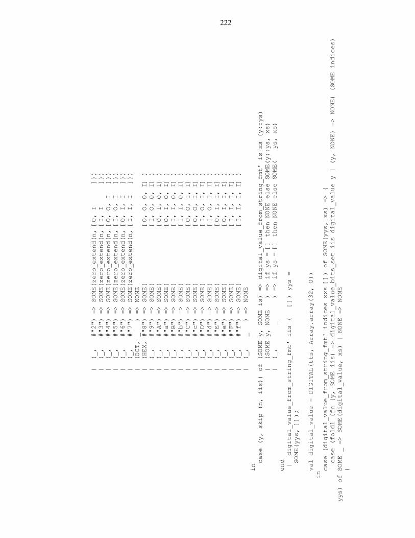
222
| (_, #"2") => SOME(zero_extend(n, [O, I ]))
| (_, #"3") => SOME(zero_extend(n, [I, I ]))
| (_, #"4") => SOME(zero_extend(n, [O, O, I ]))
| (_, #"5") => SOME(zero_extend(n, [I, O, I ]))
| (_, #"6") => SOME(zero_extend(n, [O, I, I ]))
| (_, #"7") => SOME(zero_extend(n, [I, I, I ]))
| (OCT, _ ) => NONE
| (HEX, #"8") => SOME( [O, O, O, I] )
| (_, #"9") => SOME( [I, O, O, I] )
| (_, #"A") => SOME( [O, I, O, I] )
| (_, #"a") => SOME( [O, I, O, I] )
| (_, #"B") => SOME( [I, I, O, I] )
| (_, #"b") => SOME( [I, I, O, I] )
| (_, #"C") => SOME( [O, O, I, I] )
| (_, #"c") => SOME( [O, O, I, I] )
| (_, #"D") => SOME( [I, O, I, I] )
| (_, #"d") => SOME( [I, O, I, I] )
| (_, #"E") => SOME( [O, I, I, I] )
| (_, #"e") => SOME( [O, I, I, I] )
| (_, #"F") => SOME( [I, I, I, I] )
| (_, #"f") => SOME( [I, I, I, I] )
| (_, _ ) => NONE
in
case (y, skip (n, iis)) of (SOME y, SOME is) => digital_value_from_string_fmt' is xs (y::ys)
| (SOME y, NONE ) => if ys = [] then NONE else SOME(y::ys, xs)
| (_, _ ) => if ys = [] then NONE else SOME( ys, xs)
end
| digital_value_from_string_fmt' iis ( []) yys =
SOME(yys, []);
val digital_value = DIGITAL(tts, Array.array(32, O))
in
case (digital_value_from_string_fmt' indices xxs []) of SOME(yys, xs) => (
case (foldl (fn (y, SOME iis) => digital_value_bits_set iis digital_value y | (y, NONE) => NONE) (SOME indices)
yys) of SOME _ => SOME(digital_value, xs) | NONE => NONE
)
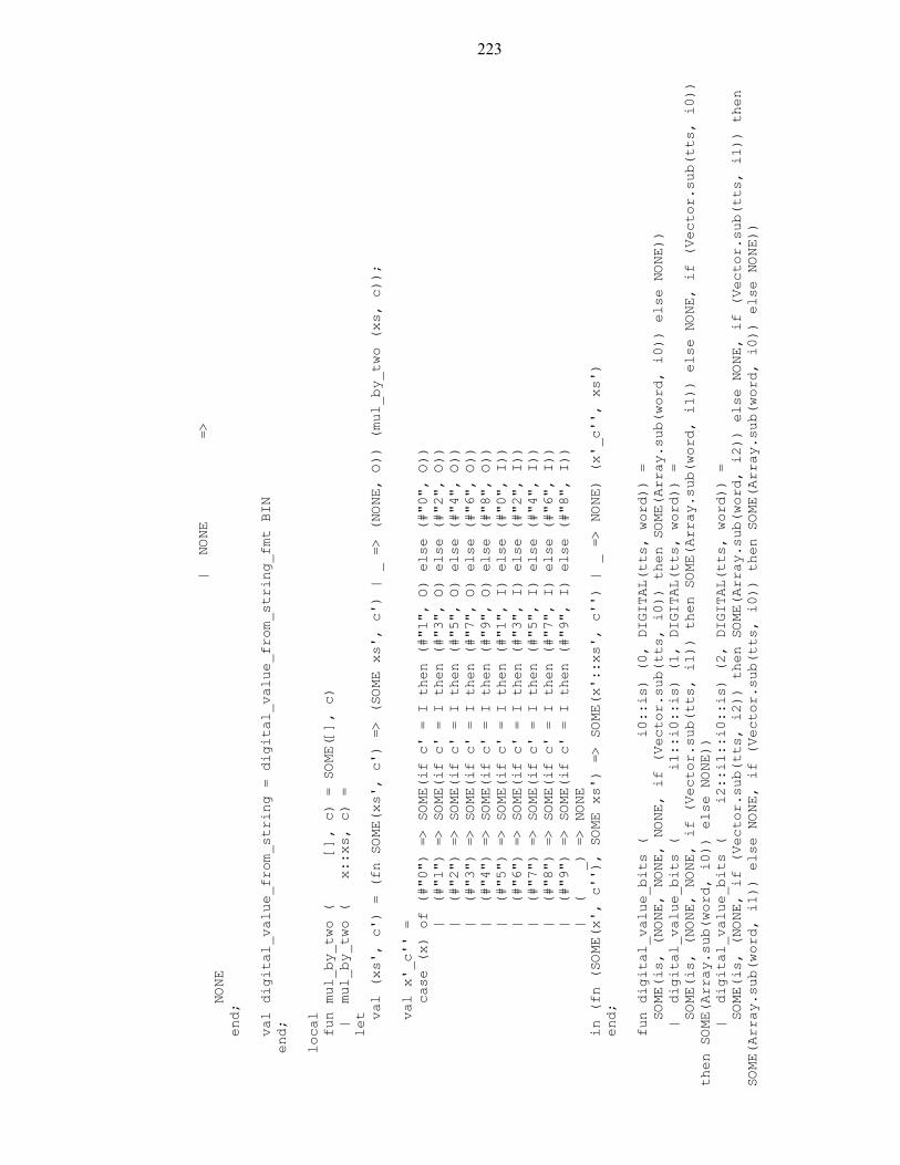
223
| NONE =>
NONE
end;
val digital_value_from_string = digital_value_from_string_fmt BIN
end;
local
fun mul_by_two ( [], c) = SOME([], c)
| mul_by_two ( x::xs, c) =
let
val (xs', c') = (fn SOME(xs', c') => (SOME xs', c') | _ => (NONE, O)) (mul_by_two (xs, c));
val x'_c'' =
case (x) of (#"0") => SOME(if c' = I then (#"1", O) else (#"0", O))
| (#"1") => SOME(if c' = I then (#"3", O) else (#"2", O))
| (#"2") => SOME(if c' = I then (#"5", O) else (#"4", O))
| (#"3") => SOME(if c' = I then (#"7", O) else (#"6", O))
| (#"4") => SOME(if c' = I then (#"9", O) else (#"8", O))
| (#"5") => SOME(if c' = I then (#"1", I) else (#"0", I))
| (#"6") => SOME(if c' = I then (#"3", I) else (#"2", I))
| (#"7") => SOME(if c' = I then (#"5", I) else (#"4", I))
| (#"8") => SOME(if c' = I then (#"7", I) else (#"6", I))
| (#"9") => SOME(if c' = I then (#"9", I) else (#"8", I))
| ( _) => NONE
in (fn (SOME(x', c''), SOME xs') => SOME(x'::xs', c'') | _ => NONE) (x'_c'', xs')
end;
fun digital_value_bits ( i0::is) (0, DIGITAL(tts, word)) =
SOME(is, (NONE, NONE, NONE, if (Vector.sub(tts, i0)) then SOME(Array.sub(word, i0)) else NONE))
| digital_value_bits ( i1::i0::is) (1, DIGITAL(tts, word)) =
SOME(is, (NONE, NONE, if (Vector.sub(tts, i1)) then SOME(Array.sub(word, i1)) else NONE, if (Vector.sub(tts, i0))
then SOME(Array.sub(word, i0)) else NONE))
| digital_value_bits ( i2::i1::i0::is) (2, DIGITAL(tts, word)) =
SOME(is, (NONE, if (Vector.sub(tts, i2)) then SOME(Array.sub(word, i2)) else NONE, if (Vector.sub(tts, i1)) then
SOME(Array.sub(word, i1)) else NONE, if (Vector.sub(tts, i0)) then SOME(Array.sub(word, i0)) else NONE))
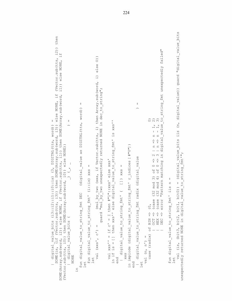
224
| digital_value_bits (i3::i2::i1::i0::is) (3, DIGITAL(tts, word)) =
SOME(is, (if (Vector.sub(tts, i3)) then SOME(Array.sub(word, i3)) else NONE, if (Vector.sub(tts, i2)) then
SOME(Array.sub(word, i2)) else NONE, if (Vector.sub(tts, i1)) then SOME(Array.sub(word, i1)) else NONE, if
(Vector.sub(tts, i0)) then SOME(Array.sub(word, i0)) else NONE))
| digital_value_bits ( _) (_, _ ) =
NONE
in
fun digital_value_to_string_fmt DEC (digital_value as DIGITAL(tts, word)) =
let
fun digital_value_to_string_fmt' (i::is) xxs =
let
val (xxs', c') = (mul_by_two (xxs, if Vector.sub(tts, i) then Array.sub(word, i) else O))
guard "mul_by_two unexpectedly returned NONE in dec_to_string";
val xxs'' = if c' = I then #"1"::xxs' else xxs'
in if is = [] then xxs'' else digital_value_to_string_fmt' is xxs''
end
| digital_value_to_string_fmt' ( []) xxs =
xxs
in implode (digital_value_to_string_fmt' r_indices [#"0"])
end
| digital_value_to_string_fmt radix (digital_value ) =
let
val (n, n') =
case (radix) of BIN => (0, 0)
| OCT => (case (32 mod 3) of 0 => 2 | n => n - 1, 2)
| HEX => (case (32 mod 4) of 0 => 3 | n => n - 1, 3)
| DEC => error "Pattern matching in digital_value_to_string_fmt unexpectedly failed"
fun digital_value_to_string_fmt' iis n =
let
val (is, (bit3, bit2, bit1, bit0)) = (digital_value_bits iis (n, digital_value)) guard "digital_value_bits
unexpectedly returned NONE in digital_value_to_string_fmt'";
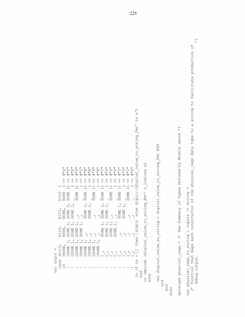
225
val digit =
case (bit3, bit2, bit1, bit0 )
of (NONE, NONE, NONE, NONE ) => #"x"
| (SOME I, SOME I, SOME I, SOME I) => #"F"
| (SOME I, SOME I, SOME I, _ ) => #"E"
| (SOME I, SOME I, _, SOME I) => #"D"
| (SOME I, SOME I, _, _ ) => #"C"
| (SOME I, _, SOME I, SOME I) => #"B"
| (SOME I, _, SOME I, _ ) => #"A"
| (SOME I, _, _, SOME I) => #"9"
| (SOME I, _, _, _ ) => #"8"
| (_, SOME I, SOME I, SOME I) => #"7"
| (_, SOME I, SOME I, _ ) => #"6"
| (_, SOME I, _, SOME I) => #"5"
| (_, SOME I, _, _ ) => #"4"
| (_, _, SOME I, SOME I) => #"3"
| (_, _, SOME I, _ ) => #"2"
| (_, _, _, SOME I) => #"1"
| (_, _, _, _ ) => #"0"
in if is = [] then [digit] else digit::(digital_value_to_string_fmt' is n')
end
in implode (digital_value_to_string_fmt' r_indices n)
end;
val digital_value_to_string = digital_value_to_string_fmt BIN
end
end
end;
datatype physical_regs = (* See Summary of Types Defined by Module above *)
val physical_regs_to_string : inputs -> string =
(* function that maps each constructor of the physical_regs data type to a string to facilitate production of
debug output. *)
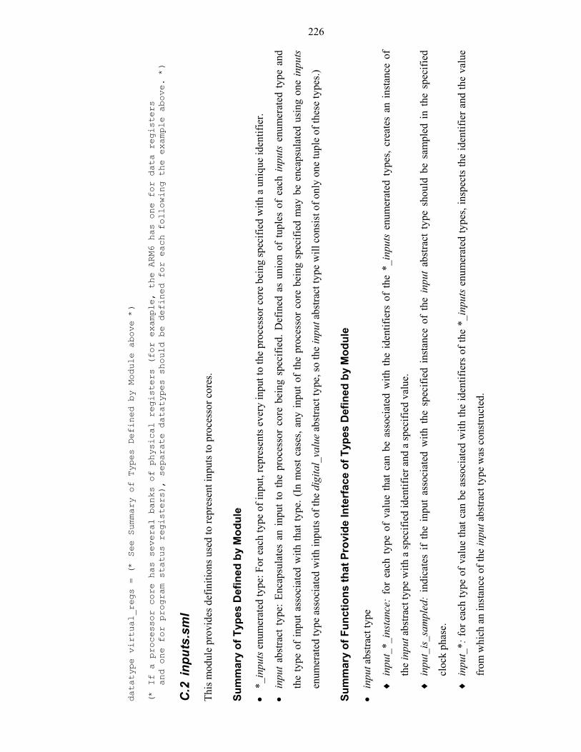
226
datatype virtual_regs = (* See Summary of Types Defined by Module above *)
(* If a processor core has several banks of physical registers (for example, the ARM6 has one for data registers
and one for program status registers), separate datatypes should be defined for each following the example above. *)
C.2
inp
uts.
sml
This
mod
ule
prov
ides
def
initi
ons u
sed
to re
pres
ent i
nput
s to
proc
esso
r cor
es.
Sum
mar
y of
Typ
es D
efin
ed b
y M
odul
e
• *_
inpu
ts e
num
erat
ed ty
pe: F
or e
ach
type
of i
nput
, rep
rese
nts e
very
inpu
t to
the
proc
esso
r cor
e be
ing
spec
ified
with
a u
niqu
e id
entif
ier.
• in
put a
bstra
ct ty
pe: E
ncap
sula
tes
an in
put t
o th
e pr
oces
sor
core
bei
ng s
peci
fied.
Def
ined
as
unio
n of
tupl
es o
f ea
ch in
puts
enu
mer
ated
type
and
the
type
of
inpu
t ass
ocia
ted
with
that
type
. (In
mos
t cas
es, a
ny in
put o
f th
e pr
oces
sor
core
bei
ng s
peci
fied
may
be
enca
psul
ated
usi
ng o
ne in
puts
enum
erat
ed ty
pe a
ssoc
iate
d w
ith in
puts
of t
he d
igita
l_va
lue
abst
ract
type
, so
the
inpu
t abs
tract
type
will
con
sist
of o
nly
one
tupl
e of
thes
e ty
pes.)
Sum
mar
y of
Fun
ctio
ns th
at P
rovi
de In
terf
ace
of T
ypes
Def
ined
by
Mod
ule
• in
put a
bstra
ct ty
pe
♦ i
nput
_*_i
nsta
nce:
for
eac
h ty
pe o
f va
lue
that
can
be
asso
ciat
ed w
ith t
he i
dent
ifier
s of
the
*_i
nput
s en
umer
ated
typ
es, c
reat
es a
n in
stan
ce o
f
the
inpu
t abs
tract
type
with
a sp
ecifi
ed id
entif
ier a
nd a
spec
ified
val
ue.
♦ i
nput
_is_
sam
pled
: in
dica
tes
if th
e in
put
asso
ciat
ed w
ith t
he s
peci
fied
inst
ance
of
the
inpu
t ab
stra
ct t
ype
shou
ld b
e sa
mpl
ed i
n th
e sp
ecifi
ed
cloc
k ph
ase.
♦ i
nput
_*: f
or e
ach
type
of v
alue
that
can
be
asso
ciat
ed w
ith th
e id
entif
iers
of t
he *
_inp
uts
enum
erat
ed ty
pes,
insp
ects
the
iden
tifie
r and
the
valu
e
from
whi
ch a
n in
stan
ce o
f the
inpu
t abs
tract
type
was
con
stru
cted
.
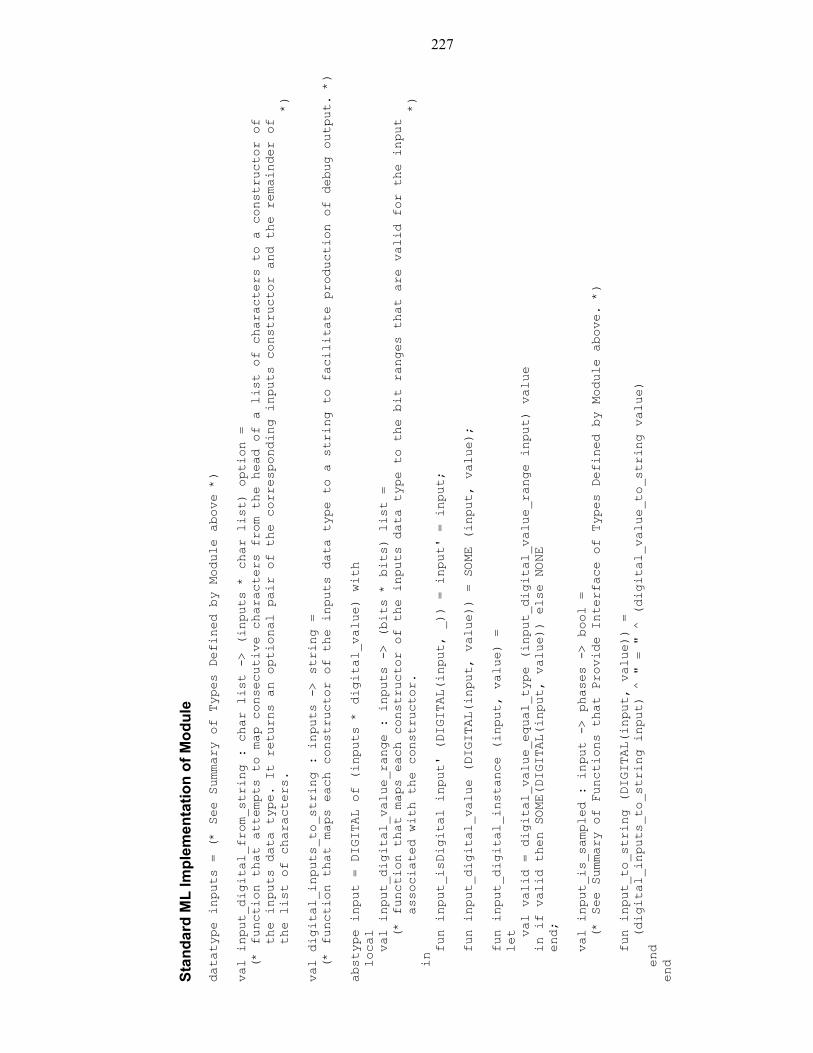
227
Stan
dard
ML
Impl
emen
tatio
n of
Mod
ule
datatype inputs = (* See Summary of Types Defined by Module above *)
val input_digital_from_string : char list -> (inputs * char list) option =
(* function that attempts to map consecutive characters from the head of a list of characters to a constructor of
the inputs data type. It returns an optional pair of the corresponding inputs constructor and the remainder of
the list of characters. *)
val digital_inputs_to_string : inputs -> string =
(* function that maps each constructor of the inputs data type to a string to facilitate production of debug output. *)
abstype input = DIGITAL of (inputs * digital_value) with
local
val input_digital_value_range : inputs -> (bits * bits) list =
(* function that maps each constructor of the inputs data type to the bit ranges that are valid for the input
associated with the constructor. *)
in
fun input_isDigital input' (DIGITAL(input, _)) = input' = input;
fun input_digital_value (DIGITAL(input, value)) = SOME (input, value);
fun input_digital_instance (input, value) =
let
val valid = digital_value_equal_type (input_digital_value_range input) value
in if valid then SOME(DIGITAL(input, value)) else NONE
end;
val input_is_sampled : input -> phases -> bool =
(* See Summary of Functions that Provide Interface of Types Defined by Module above. *)
fun input_to_string (DIGITAL(input, value)) =
(digital_inputs_to_string input) ^ " = " ^ (digital_value_to_string value)
end
end
228
C.3
bus
es.s
ml
This
mod
ule
prov
ides
def
initi
ons u
sed
to re
pres
ent b
uses
in p
roce
ssor
cor
es a
nd to
trac
e th
e va
lues
ass
ocia
ted
with
thes
e bu
ses d
urin
g si
mul
atio
n.
Sum
mar
y of
Typ
es D
efin
ed b
y M
odul
e
• *_
buse
s enu
mer
ated
type
: For
eac
h ty
pe o
f bus
, rep
rese
nts e
very
bus
of t
he p
roce
ssor
cor
e be
ing
spec
ified
with
a u
niqu
e id
entif
ier.
• bu
s ab
stra
ct ty
pe: E
ncap
sula
tes
a bu
s of
the
proc
esso
r cor
e be
ing
spec
ified
. Def
ined
as
unio
n of
tupl
es o
f eac
h bu
ses
enum
erat
ed ty
pe a
nd th
e ty
pe
of b
us a
ssoc
iate
d w
ith th
at ty
pe.
• tr
aces
uni
on ty
pe: U
nion
of e
very
type
ass
ocia
ted
with
the
buse
s enu
mer
ated
type
.
• tr
ace
abst
ract
type
: Enc
apsu
late
s va
lues
ass
ocia
ted
with
bus
es d
urin
g si
mul
atio
n. S
ee d
etai
led
disc
ussi
on in
sec
tion
2.3.
3 fo
r mor
e on
how
this
type
is c
onst
ruct
ed a
s wel
l as h
ow it
is u
sed.
Sum
mar
y of
Fun
ctio
ns th
at P
rovi
de In
terf
ace
of T
ypes
Def
ined
by
Mod
ule
• bu
s abs
tract
type
♦ b
us_*
_ins
tanc
e: fo
r eac
h ty
pe o
f val
ue th
at c
an b
e as
soci
ated
with
the
iden
tifie
rs o
f the
*_b
uses
enu
mer
ated
type
s, cr
eate
s an
inst
ance
of t
he b
us
abst
ract
type
with
the
spec
ified
iden
tifie
r and
the
spec
ified
val
ue.
♦ b
us_f
rom
_inp
ut: c
onst
ruct
s an
app
ropr
iate
inst
ance
of t
he b
us a
bstra
ct ty
pe fr
om a
n in
stan
ce o
f the
inpu
t abs
tract
type
to re
pres
ent t
he d
rivin
g of
a bu
s by
an in
put.
♦ b
us_b
uffe
r: in
dica
tes
whe
ther
the
spec
ified
inst
ance
of t
he b
us a
bstra
ct ty
pe s
houl
d be
buf
fere
d us
ing
pipe
line
latc
hes,
and
if it
shou
ld, a
t whi
ch
pipe
line
stag
e bu
ffer
ing
shou
ld b
egin
and
at w
hich
it sh
ould
end
.
229
♦ b
us_*
: fo
r ea
ch ty
pe o
f va
lue
that
can
be
asso
ciat
ed w
ith th
e id
entif
iers
of
the
*_bu
ses
enum
erat
ed ty
pes,
insp
ects
the
iden
tifie
r an
d th
e va
lue
from
whi
ch a
n in
stan
ce o
f the
bus
abs
tract
type
was
con
stru
cted
.
• tr
ace
abst
ract
type
♦ t
race
_ini
t: co
nstru
cts
an in
stan
ce o
f the
trac
e ab
stra
ct ty
pe w
ith e
lem
ents
initi
alis
ed u
sing
the
empt
y co
llect
ion
as w
ell a
s th
e sp
ecifi
ed n
umbe
r of
cloc
k cy
cles
sinc
e si
mul
atio
n be
gan
and
the
spec
ified
cur
rent
clo
ck p
hase
.
♦ t
race
_at:
mod
ifies
the
spe
cifie
d in
stan
ce o
f th
e tr
ace
abst
ract
typ
e to
sto
re t
race
inf
orm
atio
n fo
r th
e sp
ecifi
ed n
umbe
r of
clo
ck c
ycle
s si
nce
sim
ulat
ion
bega
n an
d th
e sp
ecifi
ed c
urre
nt c
lock
pha
se u
ntil
trac
e_at
is in
voke
d ag
ain.
♦ t
race
_if:
mod
ifies
the
spe
cifie
d in
stan
ce o
f th
e tr
ace
abst
ract
typ
e to
sto
re t
race
inf
orm
atio
n on
ly i
f th
e sp
ecifi
ed f
unct
ion
map
s th
e cu
rren
t
num
ber o
f clo
ck c
ycle
s sin
ce si
mul
atio
n be
gan
and
the
curr
ent c
lock
pha
se o
nto
the
bool
prim
itive
type
val
ue tr
ue.
♦ t
race
_add
_bus
es: m
odifi
es th
e sp
ecifi
ed in
stan
ce o
f the
trac
e ab
stra
ct ty
pe to
sto
re tr
ace
info
rmat
ion
abou
t the
val
ue o
f eac
h in
stan
ce o
f the
bus
abst
ract
type
in th
e sp
ecifi
ed li
st u
nles
s tra
ce in
form
atio
n sh
ould
not
be
stor
ed fo
r the
cur
rent
num
ber o
f clo
ck c
ycle
s si
nce
sim
ulat
ion
bega
n an
d
the
curr
ent c
lock
pha
se.
♦ t
race
_loo
kup_
*: in
spec
ts th
e va
lue,
if a
ny, t
hat w
as tr
aced
for
the
spec
ified
*_b
uses
enu
mer
ated
type
at t
he s
peci
fied
num
ber
of c
lock
cyc
les
sinc
e si
mul
atio
n be
gan
and
in th
e sp
ecifi
ed c
lock
pha
se.
♦ t
race
_ns_
per_
cc: m
odifi
es th
e sp
ecifi
ed in
stan
ce o
f the
trac
e ab
stra
ct ty
pe s
uch
that
eac
h cl
ock
cycl
e is
ass
umed
to ta
ke th
e sp
ecifi
ed n
umbe
r of
nano
seco
nds t
o co
mpl
ete.
♦ t
race
_sig
nal_
scal
ing:
mod
ifies
the
spec
ified
inst
ance
of
the
trac
e ab
stra
ct ty
pe s
o on
ly th
e sp
ecifi
ed p
erce
ntag
e of
the
num
ber
of n
anos
econ
ds
each
clo
ck p
hase
is a
ssum
ed to
take
is d
ivid
ed u
p ac
cord
ing
to th
e nu
mbe
r of t
imin
g gr
oups
, with
sign
als i
n th
e re
spec
tive
timin
g gr
oups
ass
umed
to b
e va
lid fr
om th
e re
leva
nt d
ivis
ion
of th
e ap
prop
riate
clo
ck p
hase
. See
the
disc
ussi
on o
f the
repr
esen
tatio
n of
trac
e in
form
atio
n as
a T
DM
L fil
e
in se
ctio
n 2.
3.3.
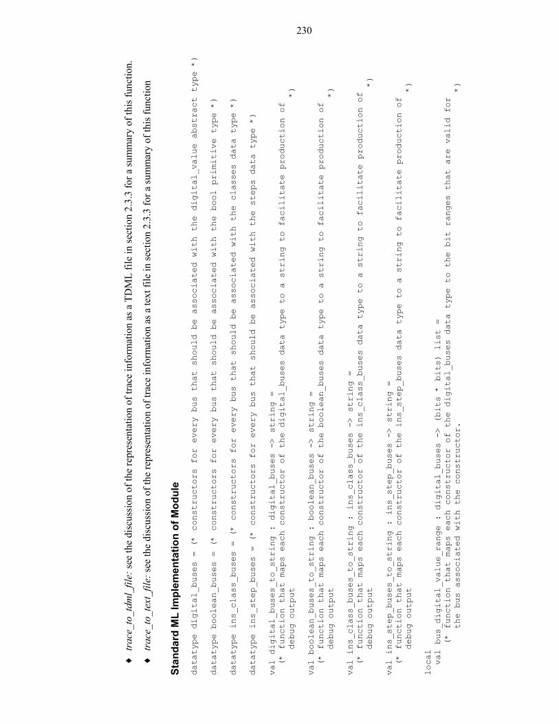
230
♦ t
race
_to_
tdm
l_fil
e: se
e th
e di
scus
sion
of t
he re
pres
enta
tion
of tr
ace
info
rmat
ion
as a
TD
ML
file
in se
ctio
n 2.
3.3
for a
sum
mar
y of
this
func
tion.
♦ t
race
_to_
text
_file
: see
the
disc
ussi
on o
f the
repr
esen
tatio
n of
trac
e in
form
atio
n as
a te
xt fi
le in
sect
ion
2.3.
3 fo
r a su
mm
ary
of th
is fu
nctio
n
Stan
dard
ML
Impl
emen
tatio
n of
Mod
ule
datatype digital_buses = (* constructors for every bus that should be associated with the digital_value abstract type *)
datatype boolean_buses = (* constructors for every bus that should be associated with the bool primitive type *)
datatype ins_class_buses = (* constructors for every bus that should be associated with the classes data type *)
datatype ins_step_buses = (* constructors for every bus that should be associated with the steps data type *)
val digital_buses_to_string : digital_buses -> string =
(* function that maps each constructor of the digital_buses data type to a string to facilitate production of
debug output *)
val boolean_buses_to_string : boolean_buses -> string =
(* function that maps each constructor of the boolean_buses data type to a string to facilitate production of
debug output *)
val ins_class_buses_to_string : ins_class_buses -> string =
(* function that maps each constructor of the ins_class_buses data type to a string to facilitate production of
debug output *)
val ins_step_buses_to_string : ins_step_buses -> string =
(* function that maps each constructor of the ins_step_buses data type to a string to facilitate production of
debug output *)
local
val bus_digital_value_range : digital_buses -> (bits * bits) list =
(* function that maps each constructor of the digital_buses data type to the bit ranges that are valid for
the bus associated with the constructor. *)
231
datatype traces = DIGITAL_TRACE of (digital_value )
| BOOLEAN_TRACE of (bool )
| INS_CLASS_TRACE of (classes )
| INS_STEP_TRACE of (steps )
in
abstype bus = DIGITAL of (digital_buses * digital_value )
| BOOLEAN of (boolean_buses * bool )
| INS_CLASS of (ins_class_buses * classes )
| INS_STEP of (ins_step_buses * steps )
and trace = TRACE of ( int ref * (int ref * phases ref) * ((int * phases -> bool) ref * bool ref)
* ( traces option array option array option array option array
* traces option array option array option array option array)
* (int ref * int ref) ) with
fun bus_isDigital digital_bus ( DIGITAL(bus, _)) = digital_bus = bus
| bus_isDigital _ _ = false;
fun bus_isBoolean boolean_bus ( BOOLEAN(bus, _)) = boolean_bus = bus
| bus_isBoolean _ _ = false;
fun bus_isInsClass ins_class_bus (INS_CLASS(bus, _)) = ins_class_bus = bus
| bus_isInsClass _ _ = false;
fun bus_isInsStep ins_step_bus ( INS_STEP(bus, _)) = ins_step_bus = bus
| bus_isInsStep _ _ = false;
fun bus_digital_value ( DIGITAL(bus, value)) = SOME (bus, value)
| bus_digital_value _ = NONE;
fun bus_boolean ( BOOLEAN(bus, value)) = SOME (bus, value)
| bus_boolean _ = NONE;
fun bus_ins_class (INS_CLASS(bus, value)) = SOME (bus, value)
| bus_ins_class _ = NONE;
fun bus_ins_step ( INS_STEP(bus, value)) = SOME (bus, value)
| bus_ins_step _ = NONE;
fun bus_digital_instance (bus, value) =
let
val valid = digital_value_equal_type (bus_digital_value_range bus) value
in if valid then SOME(DIGITAL(bus, value)) else NONE
end;
232
fun bus_boolean_instance (bus, value) =
SOME(BOOLEAN(bus, value));
fun bus_ins_class_instance (bus, value) =
SOME(INS_CLASS(bus, value));
fun bus_ins_step_instance (bus, value) =
SOME(INS_STEP(bus, value));
val bus_from_input : input -> bus option =
(* See Summary of Functions that Provide Interface of Types Defined by Module above. *)
val bus_buffer : bus -> (stages * stages) option =
(* See Summary of Functions that Provide Interface of Types Defined by Module above. *)
fun bus_to_string ( DIGITAL(bus, value)) = (digital_buses_to_string bus) ^ " = " ^ (digital_value_to_string value)
| bus_to_string ( BOOLEAN(bus, true )) = (boolean_buses_to_string bus) ^ " = " ^ ("true" )
| bus_to_string ( BOOLEAN(bus, false)) = (boolean_buses_to_string bus) ^ " = " ^ ("false" )
| bus_to_string (INS_CLASS(bus, value)) = (ins_class_buses_to_string bus) ^ " = " ^ (classes_to_string value)
| bus_to_string ( INS_STEP(bus, value)) = (ins_step_buses_to_string bus) ^ " = " ^ (steps_to_string value)
local
val bus_digital_trace : digital_buses -> phases -> (int * int) option =
(* function that associates with the specified phase and constructor of the digital_buses data type,
the timing group and position in this timing group that should be used to trace it. *)
val bus_boolean_trace : boolean_buses -> phases -> (int * int) option =
(* function that associates with the specified constructor of the boolean_buses data type,
the timing group and position in this timing group that should be used to trace it. *)
val bus_ins_class_trace : ins_class_buses -> phases -> (int * int) option =
(* function that associates with the specified phase and constructor of the ins_class_buses data type,
the timing group and position in this timing group that should be used to trace it. *)
val bus_ins_step_trace : ins_step_buses -> phases -> (int * int) option =
(* function that associates with the specified phase and constructor of the ins_step_buses data type,
the timing group and position in this timing group that should be used to trace it. *)
233
fun bus_to_trace_element ( DIGITAL(bus, value)) ph =
((bus_digital_trace bus ph) guard ("Cannot trace " ^ (digital_buses_to_string bus) ^ " in " ^
(phases_to_string ph)), DIGITAL_TRACE(value) )
| bus_to_trace_element ( BOOLEAN(bus, value)) ph =
((bus_boolean_trace bus ph) guard ("Cannot trace " ^ (boolean_buses_to_string bus) ^ " in " ^
(phases_to_string ph)), BOOLEAN_TRACE(value) )
| bus_to_trace_element (INS_CLASS(bus, value)) ph =
((bus_ins_class_trace bus ph) guard ("Cannot trace " ^ (ins_class_buses_to_string bus) ^ " in " ^
(phases_to_string ph)), INS_CLASS_TRACE(value) )
| bus_to_trace_element ( INS_STEP(bus, value)) ph =
((bus_ins_step_trace bus ph) guard ("Cannot trace " ^ (ins_step_buses_to_string bus) ^ " in " ^
(phases_to_string ph)), INS_STEP_TRACE(value) );
val bus_trace_phase : bus -> phases -> phases =
(* function that associates with the specified instance of the bus abstract type and phase the phase that
should be used to trace it. *)
val timing_groups : phases -> int =
(* function that returns the maximum number of timing groups required to trace the values of buses active in
the specified clock phase. *)
val timing_group_elements : phases -> int -> int =
(* function that returns the maximum number of positions required to trace the values of buses active in
the specified clock phase and which belong to the specified timing group. *)
val write_trace phases -> int * int -> bool =
(* function that checks whether the specified position in the specified timing group is used to trace a value
in the specified phase; if the value of a bus is valid in more than one clock phase, it should be traced
using only one clock phase. *)
fun lookup_trace_element (array, (m, n, i)) =
case (Array.sub(array, m)) of SOME group => (
case (Array.sub(group, n)) of SOME pages =>
let
val (page_number, page_entry) = (i div 10000, i mod 10000)
234
in
if page_number < Array.length pages then
case (Array.sub(pages, page_number)) of SOME page => Array.sub(page, page_entry) | NONE => NONE
else
NONE
end
| NONE =>
NONE
)
| NONE =>
NONE;
fun update_trace_element (array, (m, n, i), value) ph =
let
val group =
case (Array.sub(array, m)) of SOME group =>
group
| NONE =>
let
val group = Array.array(timing_group_elements ph m, NONE)
in (Array.update(array, m, SOME group); group)
end;
val (page_number, page_entry) = (i div 10000, i mod 10000);
val pages =
case (Array.sub(group, n)) of SOME pages =>
let
val length = Array.length pages
in
if length <= page_number then
(fn pages => (Array.update(group, n, SOME pages); pages)) (Array.tabulate(page_number + 1, fn x => if x <
length then Array.sub(pages, x) else NONE))
else
pages
end
235
| NONE =>
let
val pages = Array.array(page_number + 1, NONE)
in (Array.update(group, n, SOME pages); pages)
end;
val page =
case (Array.sub(pages, page_number)) of SOME page =>
page
| NONE =>
let
val page = Array.array(10000, NONE)
in (Array.update(pages, page_number, SOME page); page)
end
in Array.update(page, page_entry, SOME value)
end;
fun cc_to_phase (cc, PH1) = cc + cc
| cc_to_phase (cc, PH2) = cc + cc + 1;
fun phase_to_cc (phase, PH1) = (phase ) div 2
| phase_to_cc (phase, PH2) = (phase - 1) div 2
in
fun trace_init (cc, ph) =
let
val _ = if cc < 0 then error "Attempt to create trace instance with negative clock cycle" else ();
val last_phase = cc_to_phase (cc, ph)
in TRACE(ref last_phase, (ref last_phase, ref ph), (ref (fn (_, _) => true), ref true), (Array.array (timing_groups
PH1, NONE), Array.array (timing_groups PH2, NONE)), (ref 1050, ref 2))
end
fun trace_at (TRACE(phases, (phase, ph), (f, trace), traces, conf)) (cc, ph') =
let
val _ = if cc < 0 then error "Attempt to trace negative clock cycle" else ();
val phase' = cc_to_phase (cc, ph')
236
in if phase' > !phases then phases := phase' else (); phase := phase'; ph := ph'; trace := !f (cc, ph')
end;
fun trace_if (TRACE(phases, (phase, ph), (f, trace), traces, conf)) f' =
(f := f'; trace := f' (phase_to_cc (!phase, !ph), !ph));
fun trace_add_buses (TRACE(_, (phase, ph), (_, ref true), (ph1_trace, ph2_trace), conf)) =
let
val ph = !ph;
fun trace_add_bus bus =
let
val ph' = bus_trace_phase bus ph;
val ((m, n), value) = bus_to_trace_element bus ph';
in update_trace_element (case ph' of PH1 => ph1_trace | PH2 => ph2_trace, (m, n, !phase), value) ph'
end
in app (fn SOME bus => trace_add_bus bus | NONE => ())
end
| trace_add_buses (_ ) =
(fn _ => ());
fun trace_lookup_digital_value (TRACE(_, _, _, (ph1_trace, ph2_trace), conf)) bus (cc, ph) =
let
val ph' = bus_trace_phase bus ph
in (fn SOME(DIGITAL_TRACE value) => SOME(value) | _ => NONE) ((fn SOME (m, n) => lookup_trace_element (case ph'
of PH1 => ph1_trace | PH2 => ph2_trace, (m, n, cc_to_phase (cc, ph))) | _ => NONE) (bus_digital_trace bus ph'))
end;
fun trace_lookup_boolean (TRACE(_, _, _, (ph1_trace, ph2_trace), conf)) bus (cc, ph) =
let
val ph' = bus_trace_phase bus ph
in (fn SOME(BOOLEAN_TRACE value) => SOME(value) | _ => NONE) ((fn SOME (m, n) => lookup_trace_element (case ph'
of PH1 => ph1_trace | PH2 => ph2_trace, (m, n, cc_to_phase (cc, ph))) | _ => NONE) (bus_boolean_trace bus ph'))
end;
fun trace_lookup_ins_class (TRACE(_, _, _, (ph1_trace, ph2_trace), conf)) bus (cc, ph) =
let
val ph' = bus_trace_phase bus ph
237
in (fn SOME(INS_CLASS_TRACE value) => SOME(value) | _ => NONE) ((fn SOME (m, n) => lookup_trace_element (case ph'
of PH1 => ph1_trace | PH2 => ph2_trace, (m, n, cc_to_phase (cc, ph))) | _ => NONE) (bus_ins_class_trace bus ph'))
end;
fun trace_lookup_ins_step (TRACE(_, _, _, (ph1_trace, ph2_trace), conf)) bus (cc, ph) =
let
val ph' = bus_trace_phase bus ph
in (fn SOME(INS_STEP_TRACE value) => SOME(value) | _ => NONE) ((fn SOME (m, n) => lookup_trace_element (case ph'
of PH1 => ph1_trace | PH2 => ph2_trace, (m, n, cc_to_phase (cc, ph))) | _ => NONE) (bus_ins_step_trace bus ph'))
end;
fun trace_lookup_last_phase (TRACE(ref last_phase, _, _, _, _)) = last_phase;
fun trace_lookup_ns_per_cc (TRACE(_, _, _, _, (ref ns, _ ))) = ns;
fun trace_lookup_signal_scaling (TRACE(_, _, _, _, (_, ref scaling))) =
if scaling = 0 then 0 else 100 div scaling;
fun trace_ns_per_cc (TRACE(_, _, _, _, (ns, _ ))) ns' = ns := ns';
fun trace_signal_scaling (TRACE(_, _, _, _, (_, scaling))) 0 =
scaling := 0
| trace_signal_scaling (TRACE(_, _, _, _, (_, scaling))) scaling' =
if scaling' > 0 andalso scaling' <= 100 then
scaling := 100 div scaling'
else
error (Int.toString scaling' ^ " is out of bounds for trace_signal_scaling");
fun outputLine os x =
(TextIO.output (os, x); TextIO.output (os, "\n"));
local
fun write_trace_header os ((start_ns, last_ns), phases) ((i_page_number, i_page_entry), (last_page_number, j)) =
(
app (outputLine os) [
"<!DOCTYPE timing.diagram PUBLIC \"-//TDML Working Group//DTD XML-PCISTDML.DTD 19990514 Draft 1.1 Timing
Diagram Markup Language DTD//EN\" \"xml-pcistdml.dtd\">",
"<timing.diagram default.time.units=\"1E-12 s\">",
238
" <tdml.admin.info>",
" <tool.info>",
" <tdml.name>SML simulator trace file</tdml.name>",
" <tdml.type>SML simulator</tdml.type>",
" </tool.info>",
" </tdml.admin.info>",
" <sources>",
" <conn.source>",
" <connection conn.type=\"O\" id=\"CLK\"><conn.name>CLK</conn.name></connection>",
(* Note strings declaring the buses that can be traced in the processor core should be inserted here. *)
" </conn.source>",
" </sources>",
" <signal show=\"1\" show.grid=\"0\" clock=\"1\" inverted=\"1\">",
" <conn.ptr conn.id=\"CLK\"></conn.ptr>",
" <clock.info>",
" <period><number>2100</number></period>",
" <duty.cycle><number>50</number></duty.cycle>",
" <time.offset><number>0</number></time.offset>",
" <jitter.falling><number>0</number></jitter.falling>",
" <jitter.rising><number>0</number></jitter.rising>",
" <uncertainty.falling><number>0</number></uncertainty.falling>",
" <uncertainty.rising><number>0</number></uncertainty.rising>",
" </clock.info>",
" <waveform>",
" <e s=\"Z\"></e>"
];
let
val g = fn (x, (ns, flush)) => (outputLine os (" <e s=\"" ^ Int.toString (x mod 2) ^ "\" te=\"" ^
Int.toString ns ^ "\"></e>"); if flush then TextIO.flushOut os else ());
fun f (page_number, SOME page) =
Array.appi g (page, if page_number <> i_page_number then 0 else i_page_entry, if page_number <>
last_page_number then NONE else SOME j)
| f (page_number, NONE ) =
error "Array.sub unexpectedly returned NONE in write_trace_header"
in Array.appi f (phases, i_page_number, NONE)
end;
239
app (outputLine os) [
" <e te=\"" ^ last_ns ^ "\"></e>",
" </waveform>",
" </signal>"
];
TextIO.flushOut os
);
local
fun write_trace_element ( NONE) =
"s=\"Z\""
| write_trace_element (SOME( DIGITAL_TRACE(digital_value))) =
let
datatype unknown_state = NULL | PREFIXED | SUFFIXED | MIXED;
val (xxs, y) = foldr (fn (#"x", (xs, PREFIXED)) => ( xs, SUFFIXED)
| (#"x", (xs, y )) => ( xs, y )
| (x, (xs, NULL )) => (x::xs, PREFIXED)
| (x, (xs, SUFFIXED)) => (x::xs, MIXED )
| (x, (xs, y )) => (x::xs, y ))
([], NULL) (explode (digital_value_to_string_fmt BIN digital_value));
val size = length xxs
in
if size = 1 then
"s=\"" ^ implode xxs ^ "\""
else
"s=\"V\" vs=\"" ^ (if y = MIXED orelse size <= 8 then implode xxs else digital_value_to_string_fmt HEX
digital_value) ^ "\""
end
| write_trace_element (SOME( BOOLEAN_TRACE( true))) =
"s=\"V\" vs=\"true\""
| write_trace_element (SOME( BOOLEAN_TRACE( false))) =
"s=\"V\" vs=\"false\""
| write_trace_element (SOME(INS_CLASS_TRACE( ins_class))) =
"s=\"V\" vs=\"" ^ classes_to_string ins_class ^ "\""
240
| write_trace_element (SOME( INS_STEP_TRACE( ins_step))) =
"s=\"V\" vs=\"" ^ steps_to_string ins_step ^ "\""
in
fun write_trace_body os ((first_ns, last_ns), phases)
((ph1_trace, ph2_trace), max_inc)
((i_page_number, i_page_entry), (last_page_number, j)) =
let
val ph1_inc = max_inc div (timing_groups PH1);
val ph2_inc = max_inc div (timing_groups PH2);
fun h inc ((SOME traces_page, phases_page), (i, j)) =
Array.appi (fn (i, x) => let val (ns, flush) = Array.sub(phases_page, i) in outputLine os (" <e " ^
write_trace_element x ^ " te=\"" ^ Int.toString (ns + (case x of NONE => 0 | _ => inc)) ^ "\"></e>"); if flush then
TextIO.flushOut os else () end) (traces_page, i, j)
| h inc ((NONE, phases_page), (i, j)) =
Array.appi (fn (i, (ns, flush)) => (outputLine os (" <e s=\"Z\" te=\"" ^ Int.toString ns ^ "\"></e>");
if flush then TextIO.flushOut os else ())) (phases_page, i, j);
fun g ph inc ((m, n), option) = (
app (outputLine os) [
" <signal show=\"1\" show.grid=\"0\">",
" <conn.ptr conn.id=\"" ^ ph ^ "_" ^ (if m > 9 then "" else "_") ^ Int.toString (m) ^ (if n > 9 then
"_" else "__") ^ Int.toString (n) ^ "\"></conn.ptr>",
" <waveform>",
" <e s=\"Z\"></e>"
];
let
val slice = fn page_number => (if page_number <> i_page_number then 0 else i_page_entry, if page_number
<> last_page_number then NONE else SOME j)
in
case (option) of SOME array =>
Array.appi (fn (page_number, SOME phases_page) => h inc ((if page_number < Array.length array then
Array.sub(array, page_number) else NONE, phases_page), slice page_number) | _ => error "Array.sub unexpectedly returned
NONE in write_trace_body") (phases, i_page_number, NONE)
241
| NONE =>
Array.appi (fn (page_number, SOME phases_page) => h inc ((NONE, phases_page), slice page_number) | _ =>
error "Array.sub unexpectedly returned NONE in write_trace_body") (phases, i_page_number, NONE)
end;
app (outputLine os) [
" <e te=\"" ^ last_ns ^ "\"></e>",
" </waveform>",
" </signal>"
];
TextIO.flushOut os
);
fun f PH1 (m, SOME array) =
let
val inc = ph1_inc * m
in Array.appi (fn (n, x) => g "PH1" inc ((m, n), x)) (array, 0, NONE)
end
| f PH2 (m, SOME array) =
let
val inc = ph2_inc * m
in Array.appi (fn (n, x) => if write_trace PH2 (m, n) then g "PH2" inc ((m, n), x) else ()) (array, 0, NONE)
end
| f PH1 (m, NONE ) =
let
val bound = timing_group_elements PH1 m;
fun iter n = if n < bound then (g "PH1" 0 ((m, n), NONE); iter (n + 1)) else ()
in iter 0
end
| f PH2 (m, NONE ) =
let
val bound = timing_group_elements PH2 m;
fun iter n = if n < bound then (if write_trace PH2 (m, n) then g "PH2" 0 ((m, n), NONE) else (); iter (n +
1)) else ()
242
in iter 0
end
in
Array.appi (f PH1) (ph1_trace, 0, NONE);
Array.appi (f PH2) (ph2_trace, 0, NONE)
end
end;
fun write_trace_footer os ((first_ns, last_ns), phases) = (
app (outputLine os) [
" <view.group>",
" <view begin.time=\"" ^ first_ns ^ "\" end.time=\"" ^ last_ns ^ "\"></view>",
" </view.group>",
"</timing.diagram>"
]
);
fun write_trace_file (ns, scaling) traces (i, j) file =
let
val (i_page_number, i_page_entry) = ((i ) div 10000, (i ) mod 10000);
val (j_page_number, j_page_entry) = ((i + j) div 10000, (i + j) mod 10000);
val j = if i_page_number = j_page_number then j else j_page_entry;
val phases = Array.tabulate(j_page_number + 1, fn page_number => if i_page_number <= page_number then let val
base = page_number * 10000 * ns in SOME(Array.tabulate(10000, fn page_entry => (base + ns * page_entry, page_entry mod
500 = 0))) end else NONE);
val first_ns = (fn (fst, _) => Int.toString fst) (Array.sub((Array.sub(phases, i_page_number))
guard "Array.sub unexpectedly returned NONE in write_trace_file", i_page_entry));
val last_ns = (fn (fst, _) => Int.toString fst) (Array.sub((Array.sub(phases, j_page_number))
guard "Array.sub unexpectedly returned NONE in write_trace_file", j_page_entry));
val os = TextIO.openOut file
in
write_trace_header os ((first_ns, last_ns), phases)
((i_page_number, i_page_entry), (j_page_number, j));
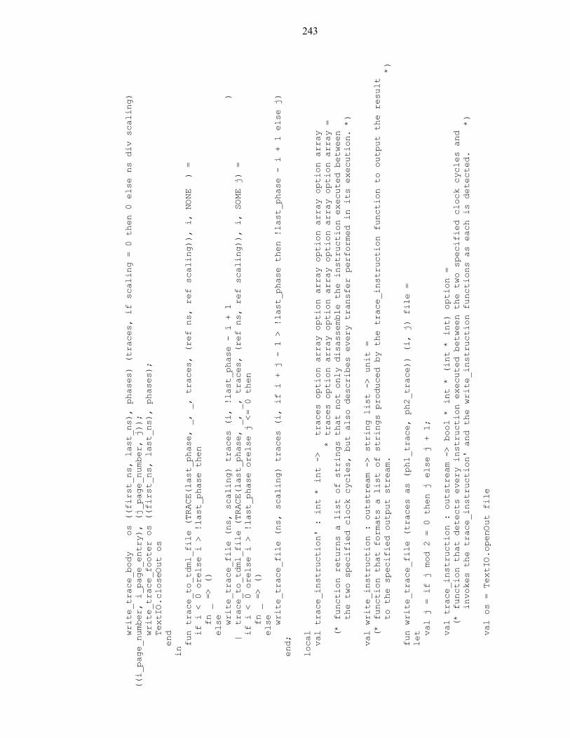
243
write_trace_body os ((first_ns, last_ns), phases) (traces, if scaling = 0 then 0 else ns div scaling)
((i_page_number, i_page_entry), (j_page_number, j));
write_trace_footer os ((first_ns, last_ns), phases);
TextIO.closeOut os
end
in
fun trace_to_tdml_file (TRACE(last_phase, _, _, traces, (ref ns, ref scaling)), i, NONE ) =
if i < 0 orelse i > !last_phase then
fn _ => ()
else
write_trace_file (ns, scaling) traces (i, !last_phase - i + 1 )
| trace_to_tdml_file (TRACE(last_phase, _, _, traces, (ref ns, ref scaling)), i, SOME j) =
if i < 0 orelse i > !last_phase orelse j <= 0 then
fn _ => ()
else
write_trace_file (ns, scaling) traces (i, if i + j - 1 > !last_phase then !last_phase - i + 1 else j)
end;
local
val trace_instruction' : int * int -> traces option array option array option array option array
* traces option array option array option array option array =
(* function returns a list of strings that not only disassemble the instruction executed between
the two specified clock cycles, but also describes every transfer performed in its execution. *)
val write_instruction : outstream -> string list -> unit =
(* function that formats a list of strings produced by the trace_instruction function to output the result
to the specified output stream. *)
fun write_trace_file (traces as (ph1_trace, ph2_trace)) (i, j) file =
let
val j = if j mod 2 = 0 then j else j + 1;
val trace_instruction : outstream -> bool * int * (int * int) option =
(* function that detects every instruction executed between the two specified clock cycles and
invokes the trace_instruction' and the write_instruction functions as each is detected. *)
val os = TextIO.openOut file
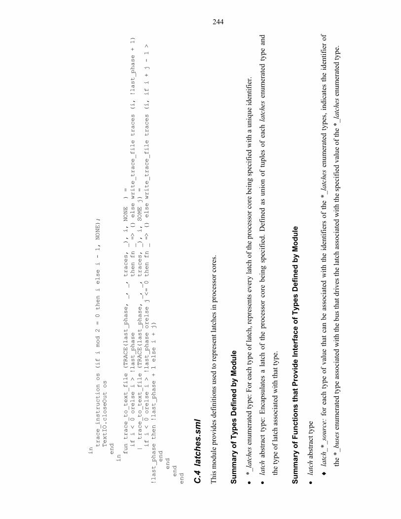
244
in
trace_instruction os (if i mod 2 = 0 then i else i - 1, NONE);
TextIO.closeOut os
end
in
fun trace_to_text_file (TRACE(last_phase, _, _, traces, _), i, NONE ) =
if i < 0 orelse i > !last_phase then fn _ => () else write_trace_file traces (i, !last_phase + 1)
| trace_to_text_file (TRACE(last_phase, _, _, traces, _), i, SOME j) =
if i < 0 orelse i > !last_phase orelse j <= 0 then fn _ => () else write_trace_file traces (i, if i + j - 1 >
!last_phase then !last_phase + 1 else i + j)
end
end
end
end
C.4
lat
ches
.sm
l
This
mod
ule
prov
ides
def
initi
ons u
sed
to re
pres
ent l
atch
es in
pro
cess
or c
ores
.
Sum
mar
y of
Typ
es D
efin
ed b
y M
odul
e
• *_
latc
hes e
num
erat
ed ty
pe: F
or e
ach
type
of l
atch
, rep
rese
nts e
very
latc
h of
the
proc
esso
r cor
e be
ing
spec
ified
with
a u
niqu
e id
entif
ier.
• la
tch
abst
ract
typ
e: E
ncap
sula
tes
a la
tch
of t
he p
roce
ssor
cor
e be
ing
spec
ified
. Def
ined
as
unio
n of
tup
les
of e
ach
latc
hes
enum
erat
ed t
ype
and
the
type
of l
atch
ass
ocia
ted
with
that
type
.
Sum
mar
y of
Fun
ctio
ns th
at P
rovi
de In
terf
ace
of T
ypes
Def
ined
by
Mod
ule
• la
tch
abst
ract
type
♦ l
atch
_*_s
ourc
e: f
or e
ach
type
of
valu
e th
at c
an b
e as
soci
ated
with
the
iden
tifie
rs o
f th
e *_
latc
hes
enum
erat
ed ty
pes,
indi
cate
s th
e id
entif
ier
of
the
*_bu
ses e
num
erat
ed ty
pe a
ssoc
iate
d w
ith th
e bu
s tha
t driv
es th
e la
tch
asso
ciat
ed w
ith th
e sp
ecifi
ed v
alue
of t
he *
_lat
ches
enu
mer
ated
type
.
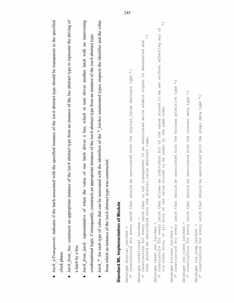
245
♦ l
atch
_isT
rans
pare
nt: i
ndic
ates
if th
e la
tch
asso
ciat
ed w
ith th
e sp
ecifi
ed in
stan
ce o
f the
latc
h ab
stra
ct ty
pe s
houl
d be
tran
spar
ent i
n th
e sp
ecifi
ed
cloc
k ph
ase.
♦ l
atch
_fro
m_b
us: c
onst
ruct
s an
app
ropr
iate
inst
ance
of t
he la
tch
abst
ract
type
from
an
inst
ance
of t
he b
us a
bstra
ct ty
pe to
repr
esen
t the
driv
ing
of
a la
tch
by a
bus
.
♦ l
atch
_fro
m_l
atch
: re
pres
enta
tive
of w
hen
the
valu
e of
one
lat
ch d
rives
a b
us,
whi
ch i
n tu
rn d
rives
ano
ther
lat
ch w
ith n
o in
terv
enin
g
com
bina
tiona
l log
ic. C
onse
quen
tly, c
onst
ruct
s an
appr
opria
te in
stan
ce o
f the
latc
h ab
stra
ct ty
pe fr
om a
n in
stan
ce o
f the
latc
h ab
stra
ct ty
pe.
♦ l
atch
_*: f
or e
ach
type
of v
alue
that
can
be
asso
ciat
ed w
ith th
e id
entif
iers
of t
he *
_lat
ches
enu
mer
ated
type
s, in
spec
ts th
e id
entif
ier a
nd th
e va
lue
from
whi
ch a
n in
stan
ce o
f the
latc
h ab
stra
ct ty
pe w
as c
onst
ruct
ed.
Stan
dard
ML
Impl
emen
tatio
n of
Mod
ule
datatype digital_latches =
(* constructors for every latch that should be associated with the digital_value abstract type *)
datatype conditional_latches =
(* constructors for every latch that is not transparent if an associated write enable signal is deasserted and
that should be associated with the digital_value abstract type. *)
datatype reset_set_latches =
(* constructors for every latch that allows an individual bit of the value stored to be set without affecting any of
its other bits, or all bits of the value stored to be reset at the same time. *)
datatype boolean_latches =
(* constructors for every latch that should be associated with the boolean primitive type *)
datatype ins_class_latches =
(* constructors for every latch that should be associated with the classes data type *)
datatype ins_step_latches =
(* constructors for every latch that should be associated with the steps data type *)
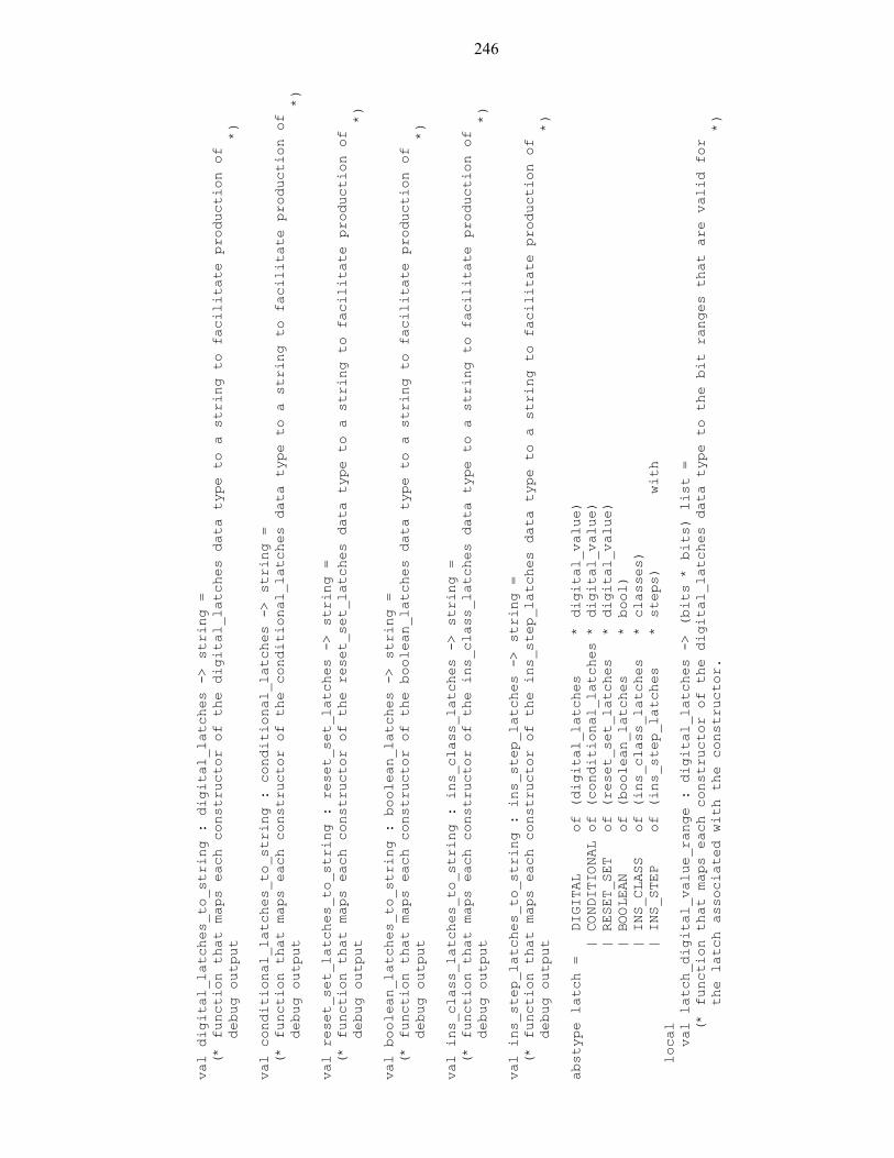
246
val digital_latches_to_string : digital_latches -> string =
(* function that maps each constructor of the digital_latches data type to a string to facilitate production of
debug output *)
val conditional_latches_to_string : conditional_latches -> string =
(* function that maps each constructor of the conditional_latches data type to a string to facilitate production of
debug output *)
val reset_set_latches_to_string : reset_set_latches -> string =
(* function that maps each constructor of the reset_set_latches data type to a string to facilitate production of
debug output *)
val boolean_latches_to_string : boolean_latches -> string =
(* function that maps each constructor of the boolean_latches data type to a string to facilitate production of
debug output *)
val ins_class_latches_to_string : ins_class_latches -> string =
(* function that maps each constructor of the ins_class_latches data type to a string to facilitate production of
debug output *)
val ins_step_latches_to_string : ins_step_latches -> string =
(* function that maps each constructor of the ins_step_latches data type to a string to facilitate production of
debug output *)
abstype latch = DIGITAL of (digital_latches * digital_value)
| CONDITIONAL of (conditional_latches * digital_value)
| RESET_SET of (reset_set_latches * digital_value)
| BOOLEAN of (boolean_latches * bool)
| INS_CLASS of (ins_class_latches * classes)
| INS_STEP of (ins_step_latches * steps) with
local
val latch_digital_value_range : digital_latches -> (bits * bits) list =
(* function that maps each constructor of the digital_latches data type to the bit ranges that are valid for
the latch associated with the constructor. *)
247
val latch_conditional_range : conditional_latches -> (bits * bits) list =
(* function that maps each constructor of the conditional_latches data type to the bit ranges that are valid for
the latch associated with the constructor. *)
val latch_reset_set_range : reset_set_latches -> (bits * bits) list =
(* function that maps each constructor of the reset_set_latches data type to the bit ranges that are valid for
the latch associated with the constructor. *)
in
fun latch_isDigital digital_latch ( DIGITAL(latch, _)) = digital_latch = latch
| latch_isDigital _ _ = false;
fun latch_isConditional conditional_latch (CONDITIONAL(latch, _)) = conditional_latch = latch
| latch_isConditional _ _ = false;
fun latch_isResetSet reset_set_latch ( RESET_SET(latch, _)) = reset_set_latch = latch
| latch_isResetSet _ _ = false;
fun latch_isBoolean boolean_latch ( BOOLEAN(latch, _)) = boolean_latch = latch
| latch_isBoolean _ _ = false;
fun latch_isInsClass ins_class_latch ( INS_CLASS(latch, _)) = ins_class_latch = latch
| latch_isInsClass _ _ = false;
fun latch_isInsStep ins_step_latch ( INS_STEP(latch, _)) = ins_step_latch = latch
| latch_isInsStep _ _ = false;
fun latch_digital_value ( DIGITAL(latch, value)) = SOME (latch, value)
| latch_digital_value _ = NONE;
fun latch_conditional (CONDITIONAL(latch, value)) = SOME (latch, value)
| latch_conditional _ = NONE;
fun latch_reset_set ( RESET_SET(latch, value)) = SOME (latch, value)
| latch_reset_set _ = NONE;
fun latch_boolean ( BOOLEAN(latch, value)) = SOME (latch, value)
| latch_boolean _ = NONE;
fun latch_ins_class ( INS_CLASS(latch, value)) = SOME (latch, value)
| latch_ins_class _ = NONE;
fun latch_ins_step ( INS_STEP(latch, value)) = SOME (latch, value)
| latch_ins_step _ = NONE;
fun latch_digital_instance (latch, value) =
let
val valid = digital_value_equal_type (latch_digital_value_range latch) value
248
in if valid then SOME(DIGITAL(latch, value)) else NONE
end;
fun latch_conditional_instance (latch, value) =
let
val valid = digital_value_equal_type (latch_conditional_range latch) value
in if valid then SOME(CONDITIONAL(latch, value)) else NONE
end;
fun latch_reset_set_instance (latch, value) =
let
val valid = digital_value_equal_type (latch_reset_set_range latch) value
in if valid then SOME(RESET_SET(latch, value)) else NONE
end;
fun latch_bool_instance (latch, value) =
SOME(BOOLEAN(latch, value));
fun latch_classes_instance (latch, value) =
SOME(INS_CLASS(latch, value));
fun latch_steps_instance (latch, value) =
SOME(INS_STEP(latch, value));
val latch_digital_source : digital_latches -> digital_buses =
(* function that maps each constructor of the digital_latches data type to the corresponding constructor of
the digital_buses data type according to whether the latch associated with the former should be driven by
the bus associated with the latter. *)
val latch_conditional_source : conditional_latches -> digital_buses =
(* function that maps each constructor of the conditonal_latches data type to the corresponding constructor of
the digital_buses data type according to whether the latch associated with the former should be driven by
the bus associated with the latter. *)
val latch_reset_set_source : reset_set_latches -> digital_buses =
(* function that maps each constructor of the reset_set_latches data type to the corresponding constructor of
249
the digital_buses data type according to whether the latch associated with the former should be driven by
the bus associated with the latter. *)
val latch_boolean_source : boolean_latches -> boolean_buses =
(* function that maps each constructor of the boolean_latches data type to the corresponding constructor of
the boolean_buses data type according to whether the latch associated with the former should be driven by
the bus associated with the latter. *)
val latch_ins_class_source : ins_class_latches -> ins_class_buses =
(* function that maps each constructor of the ins_class_latches data type to the corresponding constructor of
the ins_class_buses data type according to whether the latch associated with the former should be driven by
the bus associated with the latter. *)
val latch_ins_step_source : ins_step_latches -> ins_step_buses =
(* function that maps each constructor of the ins_step_latches data type to the corresponding constructor of
the ins_step_buses data type according to whether the latch associated with the former should be driven by
the bus associated with the latter. *)
val latch_isTransparent : latch -> phases -> bool =
(* function that examines the constructor of the latches data type used to create an instance of the latch
abstract type to determine whether the latch associated with the constructor should be transparent in
the specified clock phase. *)
val latch_conditional_write_signal : conditional_latches -> boolean_buses =
(* function that maps each constructor of the conditional_latches data type to the constructor of
the boolean_buses data type that abstracts over the write signal associated with the latch that
the former abstracts over. *)
val latch_from_bus : bus -> latch option =
(* See Summary of Functions that Provide Interface of Types Defined by Module above. *)
val latch_from_latch : latch -> (bus * latch) option =
(* See Summary of Functions that Provide Interface of Types Defined by Module above. *)
250
fun latch_to_string ( DIGITAL(latch, value)) =
(digital_latches_to_string latch) ^ " = " ^ (digital_value_to_string value)
| latch_to_string (CONDITIONAL(latch, value)) =
(conditional_latches_to_string latch) ^ " = " ^ (digital_value_to_string value)
| latch_to_string ( RESET_SET(latch, value)) =
(reset_set_latches_to_string latch) ^ " = " ^ (digital_value_to_string value)
| latch_to_string ( BOOLEAN(latch, true )) =
(boolean_latches_to_string latch) ^ " = " ^ ("true" )
| latch_to_string ( BOOLEAN(latch, false)) =
(boolean_latches_to_string latch) ^ " = " ^ ("false" )
| latch_to_string ( INS_CLASS(latch, value)) =
(ins_class_latches_to_string latch) ^ " = " ^ (classes_to_string value)
| latch_to_string ( INS_STEP(latch, value)) =
(ins_step_latches_to_string latch) ^ " = " ^ (steps_to_string value)
end
end
C.5
out
puts
.sm
l
This
mod
ule
prov
ides
def
initi
ons u
sed
to re
pres
ent o
utpu
ts o
f pro
cess
or c
ores
.
Sum
mar
y of
Typ
es D
efin
ed b
y M
odul
e
• *_
outp
uts e
num
erat
ed ty
pe: F
or e
ach
type
of o
utpu
t, re
pres
ents
eve
ry o
utpu
t of t
he p
roce
ssor
cor
e be
ing
spec
ified
with
a u
niqu
e id
entif
ier.
• ou
tput
abs
tract
type
: Enc
apsu
late
s an
out
put o
f the
pro
cess
or c
ore
bein
g sp
ecifi
ed. D
efin
ed a
s un
ion
of tu
ples
of e
ach
outp
uts
enum
erat
ed ty
pe a
nd
the
type
of
outp
ut a
ssoc
iate
d w
ith t
hat
type
. (U
sual
ly a
ny o
utpu
t of
the
pro
cess
or c
ore
bein
g sp
ecifi
ed m
ay b
e en
caps
ulat
ed u
sing
one
out
puts
enum
erat
ed ty
pe a
ssoc
iate
d w
ith o
utpu
ts o
f the
dig
ital_
valu
e ab
stra
ct ty
pe, s
o th
e ou
tput
abs
tract
type
will
con
sist
of o
nly
one
tupl
e of
thes
e ty
pes.)
251
Sum
mar
y of
Fun
ctio
ns th
at P
rovi
de In
terf
ace
of T
ypes
Def
ined
by
Mod
ule
• ou
tput
abs
tract
type
♦ o
utpu
t_*_
inst
ance
: fo
r ea
ch ty
pe o
f va
lue
that
can
be
asso
ciat
ed w
ith th
e id
entif
iers
of
the
*_ou
tput
s en
umer
ated
type
, cre
ates
an
inst
ance
of
the
outp
ut a
bstra
ct ty
pe w
ith a
spec
ified
iden
tifie
r and
a sp
ecifi
ed v
alue
.
♦ o
utpu
t_*:
for e
ach
type
of v
alue
that
can
be
asso
ciat
ed w
ith th
e id
entif
iers
of t
he *
_out
puts
enu
mer
ated
type
, ins
pect
s th
e id
entif
ier a
nd th
e va
lue
from
whi
ch th
e sp
ecifi
ed in
stan
ce o
f the
out
put a
bstra
ct ty
pe w
as c
onst
ruct
ed.
♦ o
utpu
t_is
Dri
ven:
ind
icat
es i
f th
e ou
tput
ass
ocia
ted
with
the
spe
cifie
d in
stan
ce o
f th
e ou
tput
abs
tract
typ
e sh
ould
be
driv
en i
n th
e sp
ecifi
ed
cloc
k ph
ase.
♦ o
utpu
t_fr
om_b
us:
cons
truct
s an
app
ropr
iate
ins
tanc
e of
the
out
put
abst
ract
typ
e fr
om a
n in
stan
ce o
f th
e ou
tput
abs
tract
typ
e to
rep
rese
nt
the
driv
ing
of a
n ou
tput
by
a bu
s.
♦ o
utpu
t_fr
om_l
atch
: co
nstru
cts
an a
ppro
pria
te i
nsta
nce
of t
he o
utpu
t ab
stra
ct t
ype
from
an
inst
ance
of
the
outp
ut a
bstra
ct t
ype
to r
epre
sent
the
driv
ing
of a
n ou
tput
by
a la
tch.
Stan
dard
ML
Impl
emen
tatio
n of
Mod
ule
datatype outputs = (* See Summary of Types Defined by Module above. *)
val digital_outputs_to_string : outputs -> string =
(* function that maps each constructor of the outputs data type to a string to facilitate production of debug output *)
abstype output = DIGITAL of (outputs * digital_value) with
local
val output_digital_value_range : inputs -> (bits * bits) list =
(* function that maps each constructor of the outputs data type to the bit ranges that are valid for the output
associated with the constructor. *)
in
252
fun output_isDigital output' (DIGITAL(output, _)) = output' = output;
fun output_digital_value (DIGITAL(output, value)) = SOME (output, value);
fun output_digital_instance (output, value) =
let
val valid = digital_value_equal_type (output_digital_value_range output) value
in if valid then SOME(DIGITAL(output, value)) else NONE
end;
val output_isDriven : output -> phases -> bool =
(* See Summary of Functions that Provide Interface of Types Defined by Module above. *)
val output_from_bus bus : bus -> output option =
(*See Summary of Functions that Provide Interface of Types Defined by Module above. *)
val output_from_latch latch : latch -> output option =
(* See Summary of Functions that Provide Interface of Types Defined by Module above. *)
fun output_to_string (DIGITAL(output, value)) =
(digital_outputs_to_string output) ^ " = " ^ (digital_value_to_string value)
end
end
C.6
sig
nals
.sm
l
This
mod
ule
prov
ides
def
initi
ons t
hat a
re u
sed
to e
ncap
sula
te e
very
inpu
t and
eve
ry o
utpu
t in
the
envi
ronm
ent o
f the
pro
cess
or c
ore
bein
g sp
ecifi
ed.
Sum
mar
y of
Typ
es D
efin
ed b
y M
odul
e
• co
re_i
nput
s ab
stra
ct ty
pe: E
ncap
sula
tes
ever
y in
put i
n th
e en
viro
nmen
t of
the
proc
esso
r co
re b
eing
spe
cifie
d. D
efin
ed a
s a
pair
of a
rec
ord
with
a fie
ld fo
r eac
h id
entif
ier o
f the
inpu
ts e
num
erat
ed ty
pes o
f the
opt
iona
l typ
e it
is a
ssoc
iate
d w
ith a
nd a
list
of t
he in
put a
bstra
ct ty
pe.
253
• co
re_o
utpu
ts a
bstra
ct ty
pe: E
ncap
sula
tes
ever
y ou
tput
in th
e en
viro
nmen
t of t
he p
roce
ssor
cor
e be
ing
spec
ified
. Def
ined
as
a re
cord
with
a fi
eld
for
each
iden
tifie
r of t
he o
utpu
ts e
num
erat
ed ty
pe o
f an
optio
nal t
uple
of t
he ty
pe it
is a
ssoc
iate
d w
ith a
nd th
e ou
tput
abs
tract
type
.
Sum
mar
y of
Fun
ctio
ns th
at P
rovi
de In
terf
ace
of T
ypes
Def
ined
by
Mod
ule
• co
re_i
nput
s abs
tract
type
♦ c
ore_
inpu
ts_i
nit:
cons
truct
s an
inst
ance
of t
he c
ore_
inpu
ts a
bstra
ct ty
pe w
ith th
e em
pty
colle
ctio
n.
♦ c
ore_
inpu
ts_u
pdat
e_in
put:
rem
oves
any
inst
ance
of
the
inpu
t abs
tract
type
con
stru
cted
with
the
spec
ified
*_i
nput
s en
umer
ated
type
iden
tifie
r
from
the
colle
ctio
n of
the
spec
ified
cor
e_in
puts
abs
tract
type
to re
pres
ent i
nsta
nces
whe
n th
e as
soci
ated
inpu
t has
the
unkn
own
valu
e.
♦ c
ore_
inpu
ts_u
pdat
e_fr
om_i
nput
s: a
dds
spec
ified
inst
ance
s of
the
inpu
t abs
tract
type
to th
e co
llect
ion
of th
e sp
ecifi
ed c
ore_
inpu
ts a
bstra
ct ty
pe,
repl
acin
g an
y pr
ior i
nsta
nces
con
stru
cted
with
iden
tical
val
ues o
f the
*_i
nput
s enu
mer
ated
type
.
♦ c
ore_
inpu
ts: i
nspe
cts c
olle
ctio
n of
the
spec
ified
cor
e_in
puts
abs
tract
type
as a
list
.
♦ c
ore_
inpu
ts_*
: in
spec
ts a
ny in
stan
ce in
the
colle
ctio
n of
the
spec
ified
cor
e_in
puts
abs
tract
type
ass
ocia
ted
with
the
rele
vant
inpu
t (sp
ecifi
ed a
s
part
of th
e na
me
of th
e fu
nctio
n).
♦ c
ore_
inpu
ts_l
ooku
p_in
put:
insp
ects
any
inst
ance
in th
e co
llect
ion
of th
e sp
ecifi
ed c
ore_
inpu
ts a
bstra
ct ty
pe c
onst
ruct
ed w
ith th
e sp
ecifi
ed v
alue
of th
e *_
inpu
ts e
num
erat
ed ty
pe.
• co
re_o
utpu
ts a
bstra
ct ty
pe
♦ c
ore_
outp
uts_
init:
con
stru
cts a
n in
stan
ce o
f the
cor
e_ou
tput
s abs
tract
type
with
the
empt
y co
llect
ion.
♦ c
ore_
outp
uts_
upda
te_o
utpu
ts:
rem
oves
any
inst
ance
s of
the
outp
ut a
bstra
ct ty
pe c
onst
ruct
ed w
ith id
entif
iers
of
the
*_ou
tput
s en
umer
ated
type
asso
ciat
ed w
ith o
utpu
ts t
hat
the
outp
ut_i
sDri
ven
func
tion
indi
cate
s sh
ould
be
driv
en b
y th
e pr
oces
sor
core
in
the
spec
ified
clo
ck p
hase
to re
pres
ent w
hen
the
valu
e dr
iven
is u
nkno
wn.
254
♦ c
ore_
outp
uts_
upda
te_f
rom
_out
puts
: ad
ds t
he s
peci
fied
inst
ance
s of
the
out
put
abst
ract
typ
e to
the
col
lect
ion
of t
he s
peci
fied
core
_out
puts
abst
ract
type
, rep
laci
ng a
ny p
rior i
nsta
nces
con
stru
cted
with
iden
tical
val
ues o
f the
*_o
utpu
ts e
num
erat
ed ty
pe.
♦ c
ore_
outp
uts:
insp
ects
col
lect
ion
of th
e sp
ecifi
ed c
ore_
outp
uts a
bstra
ct ty
pe a
s a li
st.
♦ c
ore_
outp
uts_
*: in
spec
ts in
stan
ce in
the
colle
ctio
n of
the
spec
ified
cor
e_ou
tput
s ab
stra
ct ty
pe a
ssoc
iate
d w
ith th
e re
leva
nt o
utpu
t (sp
ecifi
ed a
s
part
of th
e na
me
of th
e fu
nctio
n).
♦ c
ore_
outp
uts_
look
up_o
utpu
t: in
spec
ts in
stan
ce in
the
colle
ctio
n of
the
spec
ified
cor
e_ou
tput
s ab
stra
ct ty
pe c
onst
ruct
ed w
ith th
e sp
ecifi
ed v
alue
of th
e *_
outp
uts e
num
erat
ed ty
pe
Stan
dard
ML
Impl
emen
tatio
n of
Mod
ule
type input_record =
(* record with a field of the digital_value option type for each constructor of the inputs data type *)
abstype core_inputs = CORE of input_record * input list with
val core_inputs_init : unit -> core_inputs =
(* See Summary of Functions that Provide Interface of Types Defined by Module above. *)
val core_inputs_update_input : core_inputs -> inputs -> core_inputs =
(* See Summary of Functions that Provide Interface of Types Defined by Module above. *)
val core_inputs_update_from_inputs : core_inputs -> input list -> core_inputs =
(* See Summary of Functions that Provide Interface of Types Defined by Module above. *)
fun core_inputs (CORE(_, xxs)) = xxs;
(* functions should be defined for each field in the record of the core_inputs abstract type to return the value
of that field for the specified instance of the core_inputs abstract type. Each function should be named using
core_inputs_ suffixed with the name of the field it inspects. *)
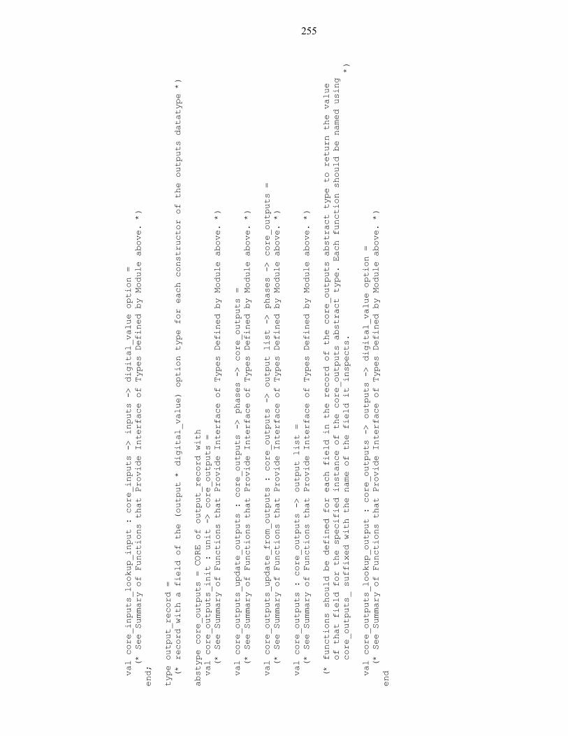
255
val core_inputs_lookup_input : core_inputs -> inputs -> digital_value option =
(* See Summary of Functions that Provide Interface of Types Defined by Module above. *)
end;
type output_record =
(* record with a field of the (output * digital_value) option type for each constructor of the outputs datatype *)
abstype core_outputs = CORE of output_record with
val core_outputs_init : unit -> core_outputs =
(* See Summary of Functions that Provide Interface of Types Defined by Module above. *)
val core_outputs_update_outputs : core_outputs -> phases -> core_outputs =
(* See Summary of Functions that Provide Interface of Types Defined by Module above. *)
val core_outputs_update_from_outputs : core_outputs -> output list -> phases -> core_outputs =
(* See Summary of Functions that Provide Interface of Types Defined by Module above. *)
val core_outputs : core_outputs -> output list =
(* See Summary of Functions that Provide Interface of Types Defined by Module above. *)
(* functions should be defined for each field in the record of the core_outputs abstract type to return the value
of that field for the specified instance of the core_outputs abstract type. Each function should be named using
core_outputs_ suffixed with the name of the field it inspects. *)
val core_outputs_lookup_output : core_outputs -> outputs -> digital_value option =
(* See Summary of Functions that Provide Interface of Types Defined by Module above. *)
end
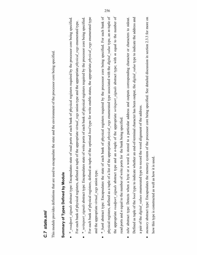
256
C.7
sta
te.s
ml
This
mod
ule
prov
ides
def
initi
ons t
hat a
re u
sed
to e
ncap
sula
te th
e st
ate
and
the
envi
ronm
ent o
f the
pro
cess
or c
ore
bein
g sp
ecifi
ed.
Sum
mar
y of
Typ
es D
efin
ed b
y M
odul
e
• *_
read
port
_sig
nals
abs
tract
type
: Enc
apsu
late
s st
ate
of re
ad p
orts
of e
ach
bank
of p
hysi
cal r
egis
ters
requ
ired
by th
e pr
oces
sor c
ore
bein
g sp
ecifi
ed.
For e
ach
bank
of p
hysi
cal r
egis
ters
, def
ined
as t
uple
of t
he a
ppro
pria
te v
irtu
al_r
egs u
nion
type
and
the
appr
opria
te p
hysi
cal_
regs
enu
mer
ated
type
.
• *_
wri
tepo
rt_s
igna
ls a
bstra
ct ty
pe: E
ncap
sula
tes s
tate
of w
rite
ports
of e
ach
bank
of p
hysi
cal r
egis
ters
requ
ired
by th
e pr
oces
sor c
ore
bein
g sp
ecifi
ed.
For e
ach
bank
of p
hysi
cal r
egis
ters
, def
ined
as
tupl
e of
the
optio
nal b
ool t
ype
for w
rite
enab
le s
tatu
s, th
e ap
prop
riate
phy
sica
l_re
gs e
num
erat
ed ty
pe
and
the
appr
opria
te v
irtu
al_r
egs u
nion
type
.
• *_
bank
abs
tract
type
: Enc
apsu
late
s th
e st
ate
of e
ach
bank
of
phys
ical
reg
iste
rs r
equi
red
by th
e pr
oces
sor
core
bei
ng s
peci
fied.
For
eac
h ba
nk o
f
phys
ical
regi
ster
s, de
fined
as
a tu
ple
of a
list
of t
he a
ppro
pria
te p
hysi
cal_
regs
enu
mer
ated
type
ass
ocia
ted
with
the
digi
tal_
valu
e ty
pe, a
n m
-tupl
e of
the
appr
opria
te r
eadp
ort_
sign
als
abst
ract
typ
e an
d an
n-tu
ple
of t
he a
ppro
pria
te w
rite
port
_sig
nals
abs
tract
typ
e; w
ith m
equ
al to
the
num
ber
of
read
por
ts a
nd n
equ
al to
the
num
ber o
f writ
e po
rts fo
r th
e ba
nk b
eing
spec
ified
.
• tu
be a
bstra
ct t
ype:
Det
ects
whe
n a
byte
or
a w
ord
is s
tore
d to
a p
artic
ular
add
ress
and
out
puts
cor
resp
ondi
ng c
hara
cter
or
char
acte
rs t
o st
dout
.
Def
ined
as
tupl
e of
the
bool
type
to in
dica
te w
heth
er a
n en
d-of
-term
inal
cha
ract
er h
as b
een
outp
ut, t
he d
igita
l_va
lue
type
to in
dica
te th
e ad
dres
s and
a pa
ir of
the
digi
tal_
valu
es e
num
erat
ed ty
pe to
reco
rd th
e w
ord
alig
nmen
t of t
he a
ddre
ss.
• m
emor
y ab
stra
ct ty
pe: E
ncap
sula
tes
the
mem
ory
syst
em o
f the
pro
cess
or c
ore
bein
g sp
ecifi
ed. S
ee d
etai
led
disc
ussi
on in
sec
tion
2.3.
3 fo
r mor
e on
how
this
type
is c
onst
ruct
ed a
s wel
l as h
ow it
is u
sed.
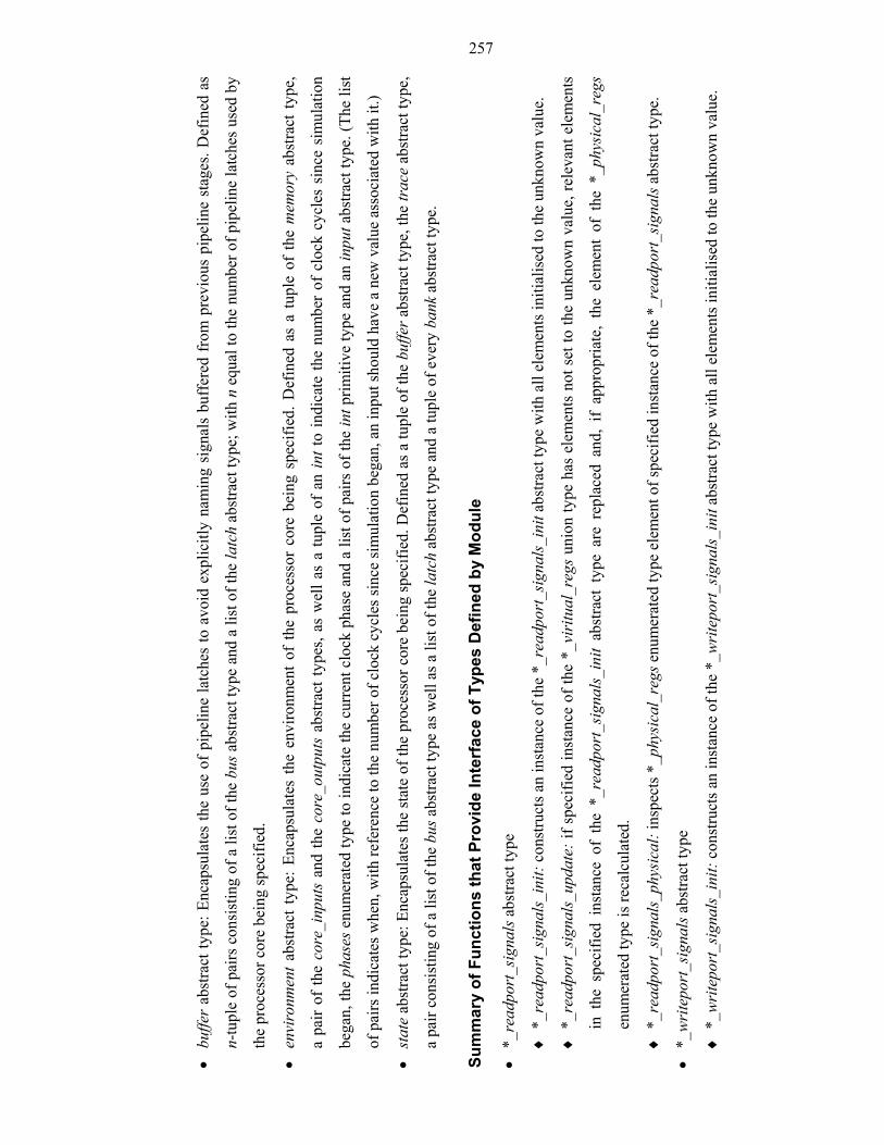
257
• bu
ffer
abst
ract
type
: Enc
apsu
late
s th
e us
e of
pip
elin
e la
tche
s to
avo
id e
xplic
itly
nam
ing
sign
als
buff
ered
from
pre
viou
s pi
pelin
e st
ages
. Def
ined
as
n-tu
ple
of p
airs
con
sist
ing
of a
list
of t
he b
us a
bstra
ct ty
pe a
nd a
list
of t
he la
tch
abst
ract
type
; with
n e
qual
to th
e nu
mbe
r of p
ipel
ine
latc
hes u
sed
by
the
proc
esso
r cor
e be
ing
spec
ified
.
• en
viro
nmen
t ab
stra
ct ty
pe: E
ncap
sula
tes
the
envi
ronm
ent o
f th
e pr
oces
sor
core
bei
ng s
peci
fied.
Def
ined
as
a tu
ple
of th
e m
emor
y ab
stra
ct ty
pe,
a pa
ir of
the
core
_inp
uts
and
the
core
_out
puts
abs
tract
type
s, as
wel
l as
a tu
ple
of a
n in
t to
indi
cate
the
num
ber
of c
lock
cyc
les
sinc
e si
mul
atio
n
bega
n, th
e ph
ases
enu
mer
ated
type
to in
dica
te th
e cu
rren
t clo
ck p
hase
and
a li
st o
f pai
rs o
f the
int p
rimiti
ve ty
pe a
nd a
n in
put a
bstra
ct ty
pe. (
The
list
of p
airs
indi
cate
s whe
n, w
ith re
fere
nce
to th
e nu
mbe
r of c
lock
cyc
les s
ince
sim
ulat
ion
bega
n, a
n in
put s
houl
d ha
ve a
new
val
ue a
ssoc
iate
d w
ith it
.)
• st
ate
abst
ract
type
: Enc
apsu
late
s the
stat
e of
the
proc
esso
r cor
e be
ing
spec
ified
. Def
ined
as a
tupl
e of
the
buffe
r abs
tract
type
, the
trac
e ab
stra
ct ty
pe,
a pa
ir co
nsis
ting
of a
list
of t
he b
us a
bstra
ct ty
pe a
s wel
l as a
list
of t
he la
tch
abst
ract
type
and
a tu
ple
of e
very
ban
k ab
stra
ct ty
pe.
Sum
mar
y of
Fun
ctio
ns th
at P
rovi
de In
terf
ace
of T
ypes
Def
ined
by
Mod
ule
• *_
read
port
_sig
nals
abs
tract
type
♦ *
_rea
dpor
t_si
gnal
s_in
it: c
onst
ruct
s an
inst
ance
of t
he *
_rea
dpor
t_si
gnal
s_in
it ab
stra
ct ty
pe w
ith a
ll el
emen
ts in
itial
ised
to th
e un
know
n va
lue.
♦ *
_rea
dpor
t_si
gnal
s_up
date
: if s
peci
fied
inst
ance
of t
he *
_vir
itual
_reg
s un
ion
type
has
ele
men
ts n
ot s
et to
the
unkn
own
valu
e, re
leva
nt e
lem
ents
in t
he s
peci
fied
inst
ance
of
the
*_re
adpo
rt_s
igna
ls_i
nit
abst
ract
typ
e ar
e re
plac
ed a
nd,
if ap
prop
riate
, th
e el
emen
t of
the
*_p
hysi
cal_
regs
enum
erat
ed ty
pe is
reca
lcul
ated
.
♦ *
_rea
dpor
t_si
gnal
s_ph
ysic
al: i
nspe
cts *
_phy
sica
l_re
gs e
num
erat
ed ty
pe e
lem
ent o
f spe
cifie
d in
stan
ce o
f the
*_r
eadp
ort_
sign
als a
bstra
ct ty
pe.
• *_
wri
tepo
rt_s
igna
ls a
bstra
ct ty
pe
♦ *
_wri
tepo
rt_s
igna
ls_i
nit:
cons
truct
s an
inst
ance
of t
he *
_wri
tepo
rt_s
igna
ls_i
nit a
bstra
ct ty
pe w
ith a
ll el
emen
ts in
itial
ised
to th
e un
know
n va
lue.
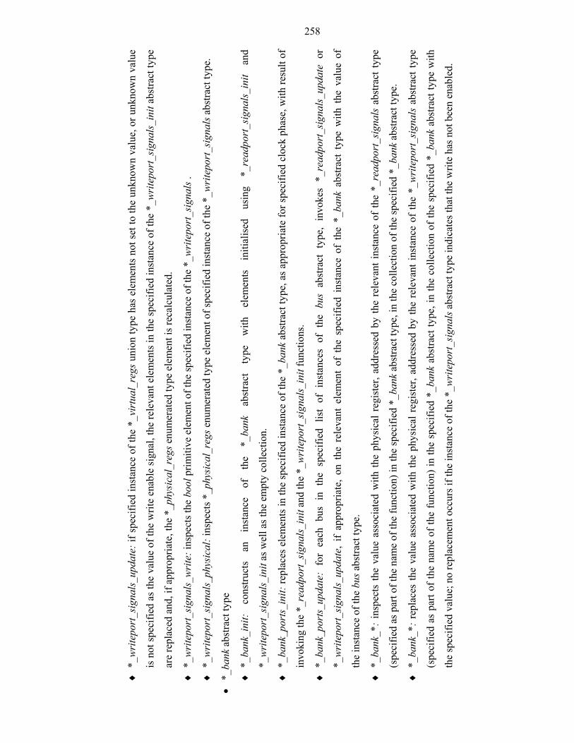
258
♦ *
_wri
tepo
rt_s
igna
ls_u
pdat
e: if
spe
cifie
d in
stan
ce o
f the
*_v
irtu
al_r
egs
unio
n ty
pe h
as e
lem
ents
not
set
to th
e un
know
n va
lue,
or u
nkno
wn
valu
e
is n
ot sp
ecifi
ed a
s the
val
ue o
f the
writ
e en
able
sign
al, t
he re
leva
nt e
lem
ents
in th
e sp
ecifi
ed in
stan
ce o
f the
*_w
rite
port
_sig
nals
_ini
t abs
tract
type
are
repl
aced
and
, if a
ppro
pria
te, t
he *
_phy
sica
l_re
gs e
num
erat
ed ty
pe e
lem
ent i
s rec
alcu
late
d.
♦ *
_wri
tepo
rt_s
igna
ls_w
rite
: ins
pect
s the
boo
l prim
itive
ele
men
t of t
he sp
ecifi
ed in
stan
ce o
f the
*_w
rite
port
_sig
nals
.
♦ *
_wri
tepo
rt_s
igna
ls_p
hysi
cal:
insp
ects
*_p
hysi
cal_
regs
enu
mer
ated
type
ele
men
t of s
peci
fied
inst
ance
of t
he *
_wri
tepo
rt_s
igna
ls a
bstra
ct ty
pe.
• *_
bank
abs
tract
type
♦ *
_ban
k_in
it:
cons
truct
s an
in
stan
ce
of
the
*_ba
nk
abst
ract
ty
pe
with
el
emen
ts
initi
alis
ed
usin
g *_
read
port
_sig
nals
_ini
t an
d
*_w
rite
port
_sig
nals
_ini
t as w
ell a
s the
em
pty
colle
ctio
n.
♦ *
_ban
k_po
rts_
init:
repl
aces
ele
men
ts in
the
spec
ified
inst
ance
of t
he *
_ban
k ab
stra
ct ty
pe, a
s ap
prop
riate
for s
peci
fied
cloc
k ph
ase,
with
resu
lt of
invo
king
the
*_re
adpo
rt_s
igna
ls_i
nit a
nd th
e *_
wri
tepo
rt_s
igna
ls_i
nit f
unct
ions
.
♦ *
_ban
k_po
rts_
upda
te:
for
each
bus
in
the
spec
ified
lis
t of
ins
tanc
es o
f th
e bu
s ab
stra
ct t
ype,
inv
okes
*_r
eadp
ort_
sign
als_
upda
te o
r
*_w
rite
port
_sig
nals
_upd
ate,
if
appr
opria
te,
on t
he r
elev
ant
elem
ent
of t
he s
peci
fied
inst
ance
of
the
*_ba
nk a
bstra
ct t
ype
with
the
val
ue o
f
the
inst
ance
of t
he b
us a
bstra
ct ty
pe.
♦ *
_ban
k_*:
insp
ects
the
valu
e as
soci
ated
with
the
phys
ical
reg
iste
r, ad
dres
sed
by th
e re
leva
nt in
stan
ce o
f th
e *_
read
port
_sig
nals
abs
tract
type
(spe
cifie
d as
par
t of t
he n
ame
of th
e fu
nctio
n) in
the
spec
ified
*_b
ank
abst
ract
type
, in
the
colle
ctio
n of
the
spec
ified
*_b
ank
abst
ract
type
.
♦ *
_ban
k_*:
rep
lace
s th
e va
lue
asso
ciat
ed w
ith th
e ph
ysic
al r
egis
ter,
addr
esse
d by
the
rele
vant
inst
ance
of
the
*_w
rite
port
_sig
nals
abs
tract
type
(spe
cifie
d as
par
t of t
he n
ame
of th
e fu
nctio
n) in
the
spec
ified
*_b
ank
abst
ract
type
, in
the
colle
ctio
n of
the
spec
ified
*_b
ank
abst
ract
type
with
the
spec
ified
val
ue; n
o re
plac
emen
t occ
urs i
f the
inst
ance
of t
he *
_wri
tepo
rt_s
igna
ls a
bstra
ct ty
pe in
dica
tes t
hat t
he w
rite
has n
ot b
een
enab
led.
259
• tu
be a
bstra
ct ty
pe
♦ t
ube_
init:
con
stru
cts a
n in
stan
ce o
f the
tube
abs
tract
type
with
a d
efau
lt ad
dres
s and
ass
umin
g no
end
-of-
term
inal
cha
ract
er h
as b
een
trans
mitt
ed.
♦ t
ube_
map
: rep
lace
s th
e ad
dres
s th
at th
e sp
ecifi
ed in
stan
ce o
f the
tube
abs
tract
type
use
s to
dete
ct w
hen
a ch
arac
ter o
r cha
ract
ers s
houl
d be
writ
ten
to st
dout
.
♦ t
ube_
eot:
insp
ects
whe
ther
the
end-
of-te
rmin
al c
hara
cter
has
bee
n tra
nsm
itted
by
the
spec
ified
inst
ance
of t
he tu
be a
bstra
ct ty
pe tr
ansm
itted
.
♦ t
ube_
tran
smit:
insp
ects
whe
ther
the
spec
ified
sto
re o
ccur
s to
the
addr
ess
mai
ntai
ned
in th
e sp
ecifi
ed in
stan
ce o
f th
e tu
be a
bstra
ct ty
pe, a
nd if
it do
es, o
utpu
ts c
orre
spon
ding
cha
ract
er o
r ch
arac
ters
to s
tdou
t; if
one
of th
ese
is th
e en
d-of
-term
inal
cha
ract
er, t
he b
ool p
rimiti
ve ty
pe u
sed
to in
dica
te th
at th
is c
hara
cter
has
bee
n tra
nsm
itted
is u
pdat
ed a
ccor
ding
ly.
• m
emor
y ab
stra
ct ty
pe
♦ m
emor
y_in
it: c
onst
ruct
s an
ins
tanc
e of
the
mem
ory
abst
ract
typ
e us
ing
the
empt
y co
llect
ion
with
no
inst
ance
of
the
tube
abs
tract
typ
e an
d
whi
ch w
ill n
ot a
bort
any
mem
ory
acce
sses
.
♦ m
emor
y_*a
bort
: in
spec
ts t
he s
peci
fied
inst
ance
of
the
mem
ory
abst
ract
typ
e an
d re
turn
s an
app
ropr
iate
ins
tanc
e of
the
inp
ut a
bstra
ct t
ype
to i
ndic
ate
if an
acc
ess
has
been
abo
rted
by t
he m
emor
y su
bsys
tem
. (T
wo
func
tions
are
nec
essa
ry i
f in
stru
ctio
n ac
cess
es m
ay b
e ab
orte
d
inde
pend
ently
of d
ata
acce
sses
.)
♦ m
emor
y_up
date
: re
plac
es th
e el
emen
ts in
the
spec
ified
inst
ance
of
the
mem
ory
abst
ract
type
that
spe
cify
an
acce
ss h
as a
borte
d, a
ccor
ding
to
whe
ther
the
acce
sses
des
crib
ed b
y th
e sp
ecifi
ed in
stan
ce o
f the
cor
e_ou
tput
s abs
tract
type
shou
ld a
bort.
♦ m
emor
y_*a
bort
_map
: re
plac
es t
he f
unct
ion
the
spec
ified
ins
tanc
e of
the
mem
ory
abst
ract
typ
e us
es t
o ch
eck
if an
acc
ess
shou
ld a
bort
with
the
spec
ified
func
tion.
(Tw
o fu
nctio
ns a
re re
quire
d if
inst
ruct
ion
acce
sses
may
abo
rt in
depe
nden
tly o
f dat
a ac
cess
es.)
♦ m
emor
y_tu
be_*
: fun
ctio
ns to
invo
ke e
ach
of th
e fu
nctio
ns d
efin
ed fo
r the
tube
abs
tract
type
on
the
inst
ance
mai
ntai
ned
by th
e sp
ecifi
ed in
stan
ce
of th
e m
emor
y ab
stra
ct ty
pe.
260
♦ *
_mem
ory_
read
, *_m
emor
y_w
rite
: bo
th th
ese
func
tions
det
erm
ine
valu
es o
f in
stan
ces
of th
e ou
tput
abs
tract
type
and
invo
ke a
loca
l fun
ctio
n,
nam
ed *
bus_
oper
atio
n, w
ith th
ese
valu
es a
nd th
e sp
ecifi
ed in
stan
ce o
f the
mem
ory
abst
ract
type
. Thi
s lo
cal f
unct
ion
to th
e m
emor
y ab
stra
ct ty
pe
patte
rn m
atch
es o
n th
e va
lues
of
outp
uts,
to d
eter
min
e th
e bu
s op
erat
ion
in p
rogr
ess
and
then
it p
erfo
rms
this
ope
ratio
n on
the
colle
ctio
n of
the
spec
ified
inst
ance
of t
he m
emor
y ab
stra
ct ty
pe. *
_mem
ory_
read
and
*_m
emor
y_w
rite
che
ck th
at th
e op
erat
ion
perf
orm
ed is
con
sist
ent w
ith
the
requ
este
d op
erat
ion,
and
dep
endi
ng o
n th
e re
ques
ted
oper
atio
n, e
ither
retu
rn th
e va
lue
read
from
mem
ory
as th
e re
leva
nt in
stan
ce o
f the
inpu
t
abst
ract
type
or t
he sp
ecifi
ed in
stan
ce o
f the
mem
ory
abst
ract
type
with
the
rele
vant
val
ue a
dded
to it
s col
lect
ion.
• bu
ffer a
bstra
ct ty
pe
♦ b
uffe
r_in
it: c
onst
ruct
s an
inst
ance
of t
he b
uffe
r abs
tract
type
with
all
elem
ents
initi
alis
ed to
the
unkn
own
valu
e.
♦ b
uffe
r_up
date
: for
eac
h pi
pelin
e la
tch,
buf
fers
the
list o
f ins
tanc
es o
f the
bus
abs
tract
type
and
the
list o
f ins
tanc
es o
f the
latc
h ab
stra
ct ty
pe fr
om
thos
e sp
ecifi
ed in
the
func
tion
invo
catio
n or
the
prec
edin
g pi
pelin
e la
tch,
as a
ppro
pria
te, i
n th
e sp
ecifi
ed in
stan
ce o
f the
buf
fer a
bstra
ct ty
pe.
♦ b
uffe
r_lo
okup
_bus
es:
retu
rns
the
list
of i
nsta
nces
of
the
bus
abst
ract
typ
e bu
ffer
ed i
n th
e sp
ecifi
ed i
nsta
nce
of t
he b
uffe
r ab
stra
ct t
ype
for
the
spec
ified
pip
elin
e la
tch.
♦ b
uffe
r_lo
okup
_lat
ches
: re
turn
s th
e lis
t of
inst
ance
s of
the
latc
h ab
stra
ct ty
pe b
uffe
red
in th
e sp
ecifi
ed in
stan
ce o
f th
e bu
ffer
abst
ract
type
for
the
spec
ified
pip
elin
e la
tch.
• st
ate
abst
ract
type
♦ s
tate
_tra
ce:
insp
ects
the
inst
ance
of
the
trac
e ab
stra
ct ty
pe m
aint
aine
d by
the
spec
ified
inst
ance
of
the
stat
e ab
stra
ct ty
pe. N
ote
that
the
trac
e
abst
ract
type
is d
efin
ed u
sing
ref
eren
ce p
rimiti
ve ty
pes
only
suc
h th
at th
e in
stan
ce re
turn
ed b
y th
is fu
nctio
n m
ay b
e us
ed to
mod
ify th
e in
stan
ce
mai
ntai
ned
by th
e sp
ecifi
ed in
stan
ce o
f the
stat
e ab
stra
ct ty
pe a
s wel
l as t
o in
spec
t it.
♦ s
tate
_ini
t: co
nstru
cts
an in
stan
ce o
f the
sta
te a
bstra
ct ty
pe w
ith e
lem
ents
initi
alis
ed u
sing
*_b
ank_
init,
buf
fer_
init
as w
ell a
s th
e em
pty
colle
ctio
n,
as a
ppro
pria
te.
261
♦ s
tate
_loo
kup_
*_bu
s: in
spec
ts th
e va
lue
asso
ciat
ed w
ith th
e sp
ecifi
ed *
_bus
es e
num
erat
ed ty
pe in
the
list o
f in
stan
ces
of th
e bu
s ab
stra
ct ty
pe
mai
ntai
ned
by th
e sp
ecifi
ed in
stan
ce o
f the
stat
e ab
stra
ct ty
pe it
self,
or i
ts in
stan
ce o
f the
buf
fer a
bstra
ct ty
pe, i
f a p
ipel
ine
latc
h is
spec
ified
.
♦ s
tate
_loo
kup_
*_la
tch:
insp
ects
the
valu
e as
soci
ated
with
the
spec
ified
*_l
atch
es e
num
erat
ed ty
pe in
the
list o
f ins
tanc
es o
f the
latc
h ab
stra
ct ty
pe
mai
ntai
ned
by th
e sp
ecifi
ed in
stan
ce o
f the
stat
e ab
stra
ct ty
pe it
self,
or i
ts in
stan
ce o
f the
buf
fer a
bstra
ct ty
pe, i
f a p
ipel
ine
latc
h is
spec
ified
.
♦ s
tate
_ins
ert_
buse
s: a
dds
the
spec
ified
inst
ance
s of
the
bus
abst
ract
type
to th
e lis
t mai
ntai
ned
by th
e sp
ecifi
ed in
stan
ce o
f the
sta
te a
bstra
ct ty
pe.
Als
o in
voke
s *_b
ank_
port
s_up
date
on
the
spec
ified
inst
ance
s of t
he b
us a
bstra
ct ty
pe.
♦ s
tate
_*_b
ank_
*: f
unct
ions
to
invo
ke e
ach
of t
he *
_ban
k_*
func
tions
def
ined
for
the
*_b
ank
abst
ract
typ
e on
the
ins
tanc
es m
aint
aine
d by
the
spec
ified
inst
ance
of t
he st
ate
abst
ract
type
.
• en
viro
nmen
t abs
tract
type
♦ e
nvir
onm
ent_
init:
con
stru
cts
an i
nsta
nce
of t
he e
nvir
onm
ent
abst
ract
typ
e w
ith e
lem
ents
ini
tialis
ed u
sing
mem
ory_
init,
cor
e_in
puts
_ini
t,
core
_out
puts
_ini
t as
wel
l as
the
min
imum
num
ber
of e
nviro
nmen
t eve
nts
(or
sche
dule
d ch
ange
s in
the
valu
es o
f ex
tern
al in
puts
) re
quire
d fo
r
the
proc
esso
r cor
e be
ing
spec
ified
to e
xit r
eset
pro
perly
.
♦ e
nvir
onm
ent_
tube
_*: f
unct
ions
to in
voke
eac
h of
the
mem
ory_
tube
_* fu
nctio
ns d
efin
ed fo
r the
mem
ory
abst
ract
type
on
inst
ance
mai
ntai
ned
by
the
spec
ified
inst
ance
of t
he e
nvir
onm
ent a
bstra
ct ty
pe.
♦ e
nvir
onm
ent_
look
up_*
_inp
ut:
invo
kes
the
core
_inp
uts_
look
up_i
nput
fu
nctio
n de
fined
fo
r th
e co
re_i
nput
s ab
stra
ct
type
on
in
stan
ce
mai
ntai
ned
by th
e sp
ecifi
ed in
stan
ce o
f the
env
iron
men
t abs
tract
type
.
♦ e
nvir
onm
ent_
look
up_*
_out
put:
invo
kes
the
core
_out
puts
_loo
kup_
outp
ut f
unct
ion
defin
ed f
or t
he c
ore_
outp
uts
abst
ract
typ
e on
ins
tanc
e
mai
ntai
ned
by th
e sp
ecifi
ed in
stan
ce o
f the
env
iron
men
t abs
tract
type
.
♦ e
nvir
onm
ent_
look
up_c
ycle
: in
spec
ts t
he s
peci
fied
inst
ance
of
the
envi
ronm
ent
abst
ract
typ
e to
det
erm
ine
the
num
ber
of c
lock
cyc
les
sinc
e
sim
ulat
ion
bega
n.
262
♦ e
nvir
onm
ent_
look
up_p
hase
: in
spec
ts
the
spec
ified
in
stan
ce
of
the
envi
ronm
ent
abst
ract
ty
pe
to
dete
rmin
e th
e va
lue
of
the
phas
es
enum
erat
ed ty
pe th
at c
orre
spon
ds to
the
cloc
k ph
ase
bein
g si
mul
ated
.
♦ e
nvir
onm
ent_
mem
ory_
*abo
rt_m
ap:
invo
kes
the
mem
ory_
*abo
rt_m
ap
func
tion
defin
ed
for
the
mem
ory
abst
ract
ty
pe
on
the
inst
ance
mai
ntai
ned
by th
e sp
ecifi
ed in
stan
ce o
f the
env
iron
men
t abs
tract
type
.
♦ e
nvir
onm
ent_
*_m
emor
y_re
ad:
invo
kes
the
*_m
emor
y_re
ad f
unct
ion
defin
ed f
or t
he m
emor
y ab
stra
ct t
ype
on t
he i
nsta
nce
mai
ntai
ned
by
the
spec
ified
inst
ance
of t
he e
nvir
onm
ent a
bstra
ct ty
pe.
♦ e
nvir
onm
ent_
*_m
emor
y_w
rite
: in
voke
s th
e *_
mem
ory_
wri
te f
unct
ion
defin
ed f
or t
he m
emor
y ab
stra
ct t
ype
on t
he i
nsta
nce
mai
ntai
ned
by
the
spec
ified
inst
ance
of t
he e
nvir
onm
ent a
bstra
ct ty
pe.
• st
ate
abst
ract
type
and
env
iron
men
t abs
tract
type
♦ s
tate
_ini
t_bu
ses:
initi
alis
es to
em
pty
colle
ctio
n th
e lis
t of b
uses
mai
ntai
ned
by th
e sp
ecifi
ed in
stan
ce o
f the
stat
e ab
stra
ct ty
pe.
♦ s
tate
_upd
ate_
buse
s: a
dds
the
inst
ance
s of
the
bus
abs
tract
typ
e co
nstru
cted
by
invo
king
bus
_fro
m_i
nput
on
ever
y in
stan
ce o
f th
e in
put
abst
ract
type
retu
rned
by
the
core
_inp
uts
func
tion
invo
ked
on th
e in
stan
ce o
f the
cor
e_in
puts
abs
tract
type
mai
ntai
ned
by th
e sp
ecifi
ed in
stan
ce
of th
e en
viro
nmen
t abs
tract
type
, whe
n in
put_
is_s
ampl
ed in
voke
d on
the
inst
ance
of
the
inpu
t abs
tract
type
indi
cate
s th
at th
e as
soci
ated
inpu
t
shou
ld b
e sa
mpl
ed in
the
cloc
k ph
ase
bein
g si
mul
ated
(ind
icat
ed b
y th
e sp
ecifi
ed in
stan
ce o
f the
env
iron
men
t abs
tract
type
).
♦ s
tate
_upd
ate_
latc
hes:
inv
okes
lat
ch_f
rom
_bus
and
lat
ch_f
rom
_lat
ch,
as r
equi
red,
to
cons
truct
new
ins
tanc
es o
f th
e la
tch
abst
ract
typ
e.
latc
h_is
Tran
spar
ent
is u
sed,
with
ref
eren
ce t
o th
e cl
ock
phas
e be
ing
sim
ulat
ed (
as i
ndic
ated
by
the
spec
ified
ins
tanc
e of
the
env
iron
men
t
abst
ract
type
), to
rem
ove
inst
ance
s of
the
latc
h ab
stra
ct ty
pe f
rom
the
colle
ctio
n m
aint
aine
d by
the
spec
ified
inst
ance
of
the
stat
e ab
stra
ct ty
pe
and
add
the
new
inst
ance
s acc
ordi
ng to
whe
n th
e as
soci
ated
latc
h sh
ould
be
trans
pare
nt.
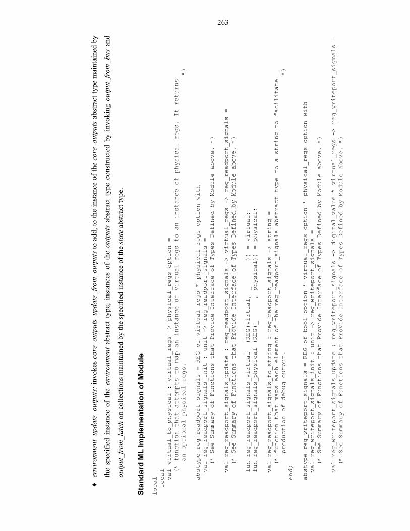
263
♦ e
nvir
onm
ent_
upda
te_o
utpu
ts: i
nvok
es c
ore_
outp
uts_
upda
te_f
rom
_out
puts
to a
dd, t
o th
e in
stan
ce o
f the
cor
e_ou
tput
s ab
stra
ct ty
pe m
aint
aine
d by
the
spec
ified
ins
tanc
e of
the
env
iron
men
t ab
stra
ct t
ype,
ins
tanc
es o
f th
e ou
tput
s ab
stra
ct t
ype
cons
truct
ed b
y in
voki
ng o
utpu
t_fr
om_b
us a
nd
outp
ut_f
rom
_lat
ch o
n co
llect
ions
mai
ntai
ned
by th
e sp
ecifi
ed in
stan
ce o
f the
stat
e ab
stra
ct ty
pe.
Stan
dard
ML
Impl
emen
tatio
n of
Mod
ule
local
local
val virtual_to_physical : virtual_regs -> physical_regs option =
(* function that attempts to map an instance of virtual_regs to an instance of physical_regs. It returns
an optional physical_regs. *)
abstype reg_readport_signals = REG of virtual_regs * physical_regs option with
val reg_readport_signals_init : unit -> reg_readport_signals =
(* See Summary of Functions that Provide Interface of Types Defined by Module above. *)
val reg_readport_signals_update : reg_readport_signals -> virtual_regs -> reg_readport_signals =
(* See Summary of Functions that Provide Interface of Types Defined by Module above. *)
fun reg_readport_signals_virtual (REG(virtual, _ )) = virtual;
fun reg_readport_signals_physical (REG(_ , physical)) = physical;
val reg_readport_signals_to_string : reg_readport_signals -> string =
(* function that maps each element of the reg_readport_signals abstract type to a string to facilitate
production of debug output. *)
end;
abstype reg_writeport_signals = REG of bool option * virtual_regs option * physical_regs option with
val reg_writeport_signals_init : unit -> reg_writeport_signals =
(* See Summary of Functions that Provide Interface of Types Defined by Module above. *)
val reg_writeport_signals_update : reg_writeport_signals -> digital_value * virtual_regs -> reg_writeport_signals =
(* See Summary of Functions that Provide Interface of Types Defined by Module above. *)
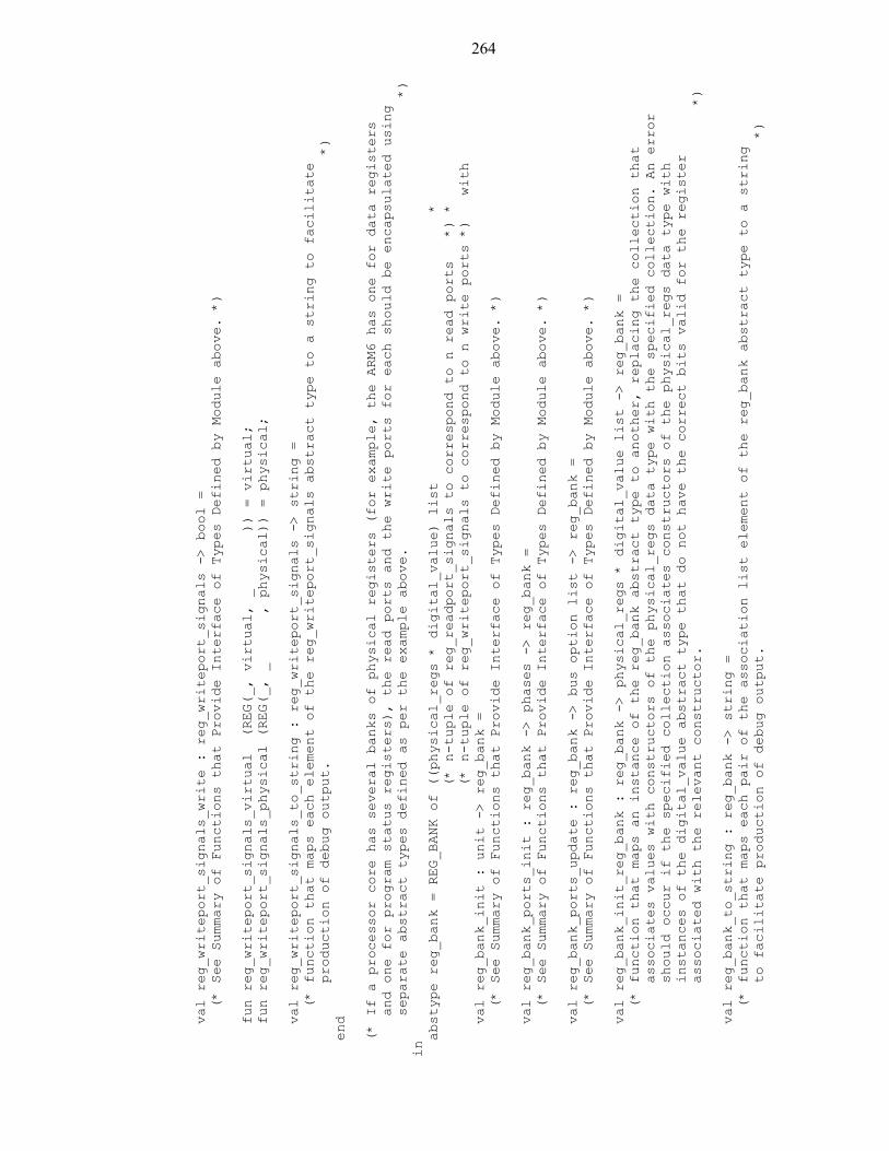
264
val reg_writeport_signals_write : reg_writeport_signals -> bool =
(* See Summary of Functions that Provide Interface of Types Defined by Module above. *)
fun reg_writeport_signals_virtual (REG(_, virtual, _ )) = virtual;
fun reg_writeport_signals_physical (REG(_, _ , physical)) = physical;
val reg_writeport_signals_to_string : reg_writeport_signals -> string =
(* function that maps each element of the reg_writeport_signals abstract type to a string to facilitate
production of debug output. *)
end
(* If a processor core has several banks of physical registers (for example, the ARM6 has one for data registers
and one for program status registers), the read ports and the write ports for each should be encapsulated using
separate abstract types defined as per the example above. *)
in
abstype reg_bank = REG_BANK of ((physical_regs * digital_value) list *
(* n-tuple of reg_readport_signals to correspond to n read ports *) *
(* n-tuple of reg_writeport_signals to correspond to n write ports *) with
val reg_bank_init : unit -> reg_bank =
(* See Summary of Functions that Provide Interface of Types Defined by Module above. *)
val reg_bank_ports_init : reg_bank -> phases -> reg_bank =
(* See Summary of Functions that Provide Interface of Types Defined by Module above. *)
val reg_bank_ports_update : reg_bank -> bus option list -> reg_bank =
(* See Summary of Functions that Provide Interface of Types Defined by Module above. *)
val reg_bank_init_reg_bank : reg_bank -> physical_regs * digital_value list -> reg_bank =
(* function that maps an instance of the reg_bank abstract type to another, replacing the collection that
associates values with constructors of the physical_regs data type with the specified collection. An error
should occur if the specified collection associates constructors of the physical_regs data type with
instances of the digital_value abstract type that do not have the correct bits valid for the register
associated with the relevant constructor. *)
val reg_bank_to_string : reg_bank -> string =
(* function that maps each pair of the association list element of the reg_bank abstract type to a string
to facilitate production of debug output. *)
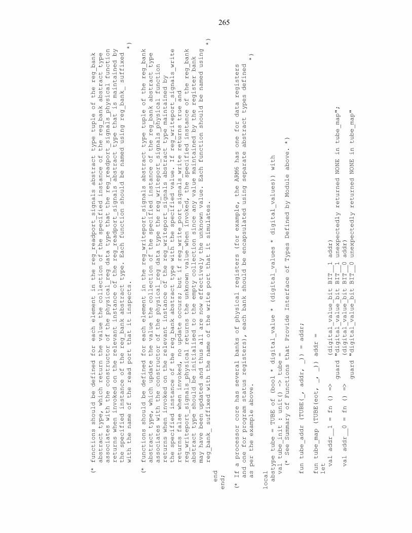
265
(* functions should be defined for each element in the reg_readport_signals abstract type tuple of the reg_bank
abstract type, which return the value the collection of the specified instance of the reg_bank abstract type
associates with the constructor of the physical_reg data type that the reg_readport_signals_physical function
returns when invoked on the relevant instance of the reg_readport_signals abstract type that is maintained by
the specified instance of the reg_bank abstract type. Each function should be named using reg_bank_ suffixed
with the name of the read port that it inspects. *)
(* functions should be defined for each element in the reg_writeport_signals abstract type tuple of the reg_bank
abstract type, which update the value the collection of the specified instance of the reg_bank abstract type
associates with the constructor of the physical_reg data type the reg_writeport_signals_physical function
returns when invoked on the relevant instance of the reg_writeport_signals abstract type maintained by
the specified instance of the reg_bank abstract type with the specified value. If reg_writeport_signals_write
returns false when invoked, no update occurs; but if reg_write_port_signals_write returns true and
reg_writeport_signals_physical returns the unknown value when invoked, the specified instance of the reg_bank
abstract type should be initialised to the empty collection since any value maintained by the register bank
may have been updated and thus all are now effectively the unknown value. Each function should be named using
reg_bank_ suffixed with the name of the write port that it simulates. *)
end
end;
(* If a processor core has several banks of physical registers (for example, the ARM6 has one for data registers
and one for program status registers), each bank should be encapsulated using separate abstract types defined
as per the example above. *)
local
abstype tube = TUBE of (bool * digital_value * (digital_values * digital_values)) with
val tube_init : unit() -> tube =
(* See Summary of Functions that Provide Interface of Types Defined by Module above. *)
fun tube_addr (TUBE(_, addr, _)) = addr;
fun tube_map (TUBE(eot, _, _)) addr =
let
val addr__1 = fn () => (digital_value_bit BIT__1 addr)
guard "digital_value_bit BIT__1 unexpectedly returned NONE in tube_map";
val addr__0 = fn () => (digital_value_bit BIT__0 addr)
guard "digital_value_bit BIT__0 unexpectedly returned NONE in tube_map"
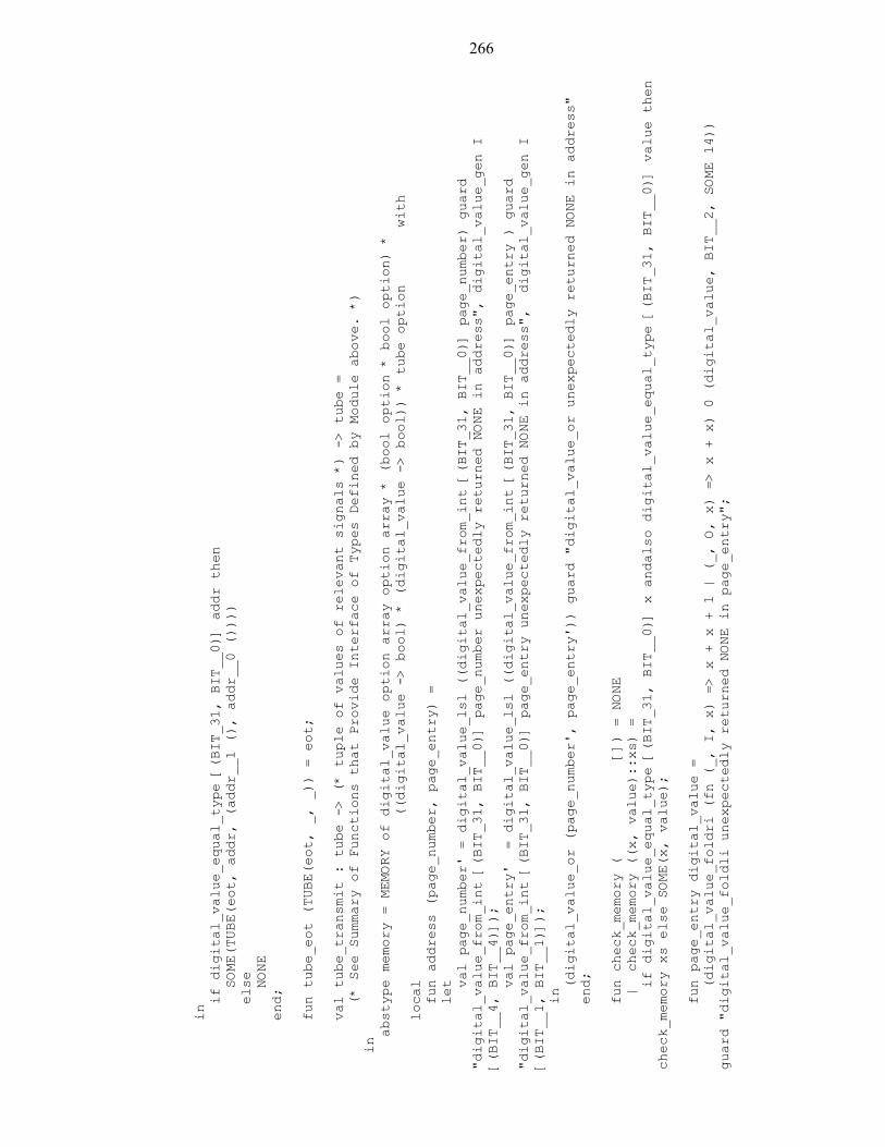
266
in
if digital_value_equal_type [(BIT_31, BIT__0)] addr then
SOME(TUBE(eot, addr, (addr__1 (), addr__0 ())))
else
NONE
end;
fun tube_eot (TUBE(eot, _, _)) = eot;
val tube_transmit : tube -> (* tuple of values of relevant signals *) -> tube =
(* See Summary of Functions that Provide Interface of Types Defined by Module above. *)
in
abstype memory = MEMORY of digital_value option array option array * (bool option * bool option) *
((digital_value -> bool) * (digital_value -> bool)) * tube option with
local
fun address (page_number, page_entry) =
let
val page_number' = digital_value_lsl ((digital_value_from_int [(BIT_31, BIT__0)] page_number) guard
"digital_value_from_int [(BIT_31, BIT__0)] page_number unexpectedly returned NONE in address", digital_value_gen I
[(BIT__4, BIT__4)]);
val page_entry' = digital_value_lsl ((digital_value_from_int [(BIT_31, BIT__0)] page_entry ) guard
"digital_value_from_int [(BIT_31, BIT__0)] page_entry unexpectedly returned NONE in address", digital_value_gen I
[(BIT__1, BIT__1)]);
in
(digital_value_or (page_number', page_entry')) guard "digital_value_or unexpectedly returned NONE in address"
end;
fun check_memory ( []) = NONE
| check_memory ((x, value)::xs) =
if digital_value_equal_type [(BIT_31, BIT__0)] x andalso digital_value_equal_type [(BIT_31, BIT__0)] value then
check_memory xs else SOME(x, value);
fun page_entry digital_value =
(digital_value_foldri (fn (_, I, x) => x + x + 1 | (_, O, x) => x + x) 0 (digital_value, BIT__2, SOME 14))
guard "digital_value_foldli unexpectedly returned NONE in page_entry";
267
fun page_number digital_value =
(digital_value_foldri (fn (_, I, x) => x + x + 1 | (_, O, x) => x + x) 0 (digital_value, BIT_16, NONE)) guard
"digital_value_foldli unexpectedly returned NONE in page_number";
fun word_align digital_value = (
fn SOME digital_value' =>
(digital_value_bit_set BIT__1 digital_value' O) guard "digital_value_bit_set BIT__1 unexpectedly returned
NONE in word_align"
| NONE =>
(fn SOME digital_value' => digital_value'
| NONE => digital_value ) (digital_value_bit_set BIT__1 digital_value O)
) (digital_value_bit_set BIT__0 digital_value O);
fun delete addr pages =
case (Array.sub(pages, page_number addr)) of (SOME page) =>
Array.update(page, page_entry addr, NONE)
| (NONE ) =>
();
fun find addr pages =
case (Array.sub(pages, page_number addr)) of (SOME page) =>
Array.sub(page, page_entry addr)
| (NONE ) =>
NONE;
fun insert addr pages value' =
let
val page_number = page_number addr;
val page_entry = page_entry addr
in
case (Array.sub(pages, page_number)) of (SOME page) => (
case (Array.sub(page, page_entry)) of (SOME value) =>
Array.update (page, page_entry, SOME((digital_value_replace (value, value'))
guard "digital_value_replace unexpectedly returned NONE in insert"))
268
| (NONE ) =>
Array.update (page, page_entry, SOME((digital_value_pad O [(BIT_31, BIT__0)] value')
guard "digital_value_pad unexpectedly returned NONE in insert"))
)
| (NONE ) =>
let
val page = Array.array(16384, NONE);
val value' = (digital_value_pad O [(BIT_31, BIT__0)] value')
guard "digital_value_pad unexpectedly returned NONE in insert"
in
Array.update(page, page_entry, SOME value');
Array.update(pages, page_number, SOME page )
end
end;
(* the dbus_operation and the ibus_operation functions should be defined to pattern match on the values of
relevant outputs and thus determine the bus operation, if any, in progress, such that it can perform
this operation on the collection of the specified instance of the memory abstract type. These functions
should return a pair of the optional memory abstract type and the optional digital_value abstract type.
This pair should include the updated instance of the memory abstract type when the *bus_operation function
performed a memory write bus operation and the value read from memory as a digital_value abstract type
when the *bus_operation function performed a memory read bus operation. *)
in
fun memory_init() =
MEMORY(Array.array(65536, NONE), (SOME false, SOME false), (fn x => false, fn x => false), NONE);
fun memory_init_memory (MEMORY(_, aborts, abort_maps, tube)) memory =
case (check_memory memory) of NONE =>
let
val memory' = Array.array(65536, NONE);
val _ = app (fn (addr, word) => insert addr memory' word) memory
in MEMORY(memory', aborts, abort_maps, tube)
end
269
| SOME(x, value) =>
error ("(" ^ (digital_value_to_string x) ^ ", " ^ (digital_value_to_string value) ^ ") is not of the proper
type to describe a memory location in memory_init_memory");
val memory_dabort : memory -> input option =
(* See Summary of Functions that Provide Interface of Types Defined by Module above. *)
val memory_iabort : memory -> input option =
(* See Summary of Functions that Provide Interface of Types Defined by Module above. *)
val memory_update : memory -> core_outputs -> memory =
(* See Summary of Functions that Provide Interface of Types Defined by Module above. *)
fun memory_dabort_map (MEMORY(memory, aborts, (_, iabort_map), tube)) dabort_map =
MEMORY(memory, aborts, (dabort_map, iabort_map), tube);
fun memory_iabort_map (MEMORY(memory, aborts, (dabort_map, _ ), tube)) iabort_map =
MEMORY(memory, aborts, (dabort_map, iabort_map), tube);
fun memory_to_string (MEMORY(memory, _, _, _)) =
Array.foldri (fn (i, SOME page, s) => Array.foldri (fn (j, SOME word, s) => s ^ "0x" ^
(digital_value_to_string_fmt HEX (address (i, j))) ^ "\t0x" ^ (digital_value_to_string_fmt HEX word) ^ "\n" | (j, NONE,
s) => s) s (page, 0, NONE) | (i, NONE, s) => s) "" (memory, 0, NONE);
fun memory_tube_init (MEMORY(memory, aborts, abort_maps, _ )) =
MEMORY(memory, aborts, abort_maps, SOME(tube_init()));
fun memory_tube_map (MEMORY(memory, aborts, abort_maps, SOME tube)) addr =
(fn SOME tube' => SOME(MEMORY(memory, aborts, abort_maps, SOME tube')) | _ => NONE) (tube_map tube addr)
| memory_tube_map (MEMORY(memory, aborts, abort_maps, NONE )) addr =
(fn SOME tube' => SOME(MEMORY(memory, aborts, abort_maps, SOME tube')) | _ => NONE) (tube_map (tube_init())
addr);
fun memory_tube_unmap (MEMORY(memory, aborts, abort_maps, _ )) =
MEMORY(memory, aborts, abort_maps, NONE);
fun memory_tube_addr (MEMORY(_, _, _, tube)) =
(fn SOME tube => SOME(tube_addr tube) | _ => NONE) tube;
fun memory_tube_eot (MEMORY(_, _, _, tube)) =
(fn SOME tube => SOME(tube_eot tube) | _ => NONE) tube;
270
val data_memory_read : memory -> outputs -> input option =
(* See Summary of Functions that Provide Interface of Types Defined by Module above. *)
val data_memory_write : memory -> outputs -> memory option =
(* See Summary of Functions that Provide Interface of Types Defined by Module above. *)
val instruction_memory_read : memory -> outputs -> input option =
(* See Summary of Functions that Provide Interface of Types Defined by Module above. *)
end
end
end;
abstype buffer = BUFFER of (* See Summary of Types Defined by Module above. *) with
val buffer_init : unit -> buffer =
(* See Summary of Functions that Provide Interface of Types Defined by Module above. *)
val buffer_update buffer -> bus list * latch list -> buffer =
(* See Summary of Functions that Provide Interface of Types Defined by Module above. *)
val buffer_loookup_buses buffer -> stages -> bus list =
(* See Summary of Functions that Provide Interface of Types Defined by Module above. *)
val buffer_loookup_latches buffer -> stages -> latch list =
(* See Summary of Functions that Provide Interface of Types Defined by Module above. *)
end
in
abstype environment = ENVIRONMENT of memory * (core_inputs * core_outputs) * (int * phases * (int * input) list)
and state = STATE of (* tuple of physical register banks *) * (bus list * latch list) * buffer * trace with
fun state_trace (STATE(_, _, _, trace)) = trace;
val state_init : unit -> state =
(* See Summary of Functions that Provide Interface of Types Defined by Module above. *)
(* Functions should be defined to invoke the functions suffixed with _init and _to_string that are defined for
each *_bank abstract type on the instances maintained by the specified instance of the state abstract type. *)
271
local
fun find f x ( [] ) = NONE
| find f x (x'::xs') = case (f x') of SOME(x'', value) => if x = x'' then SOME(value) else find f x xs'
| NONE => find f x xs'
in
fun state_lookup_digital_value_bus (STATE(banks, (buses, _), _, _)) (NONE ) digital_value_bus =
find bus_digital_value digital_value_bus (buses )
| state_lookup_digital_value_bus (STATE(banks, (buses, _), buffer, _)) (SOME stg) digital_value_bus =
find bus_digital_value digital_value_bus (buffer_lookup_buses buffer stg);
fun state_lookup_boolean_bus (STATE(banks, (buses, _), _, _)) (NONE ) boolean_bus =
find bus_boolean boolean_bus (buses )
| state_lookup_boolean_bus (STATE(banks, (buses, _), buffer, _)) (SOME stg) boolean_bus =
find bus_boolean boolean_bus (buffer_lookup_buses buffer stg);
fun state_lookup_ins_class_bus (STATE(banks, (buses, _), _, _)) (NONE ) ins_class_bus =
find bus_ins_class ins_class_bus (buses )
| state_lookup_ins_class_bus (STATE(banks, (buses, _), buffer, _)) (SOME stg) ins_class_bus =
find bus_ins_class ins_class_bus (buffer_lookup_buses buffer stg);
fun state_lookup_ins_step_bus (STATE(banks, (buses, _), _, _)) (NONE ) ins_step_bus =
find bus_ins_step ins_step_bus (buses )
| state_lookup_ins_step_bus (STATE(banks, (buses, _), buffer, _)) (SOME stg) ins_step_bus =
find bus_ins_step ins_step_bus (buffer_lookup_buses buffer stg);
fun state_lookup_digital_value_latch (STATE(banks, (_, latches), _, _)) (NONE ) digital_value_latch =
find latch_digital_value digital_value_latch (latches )
| state_lookup_digital_value_latch (STATE(banks, (_, latches), buffer, _)) (SOME stg) digital_value_latch =
find latch_digital_value digital_value_latch (buffer_lookup_latches buffer stg);
fun state_lookup_conditional_latch (STATE(banks, (_, latches), _, _)) (NONE ) conditional_latch =
find latch_conditional conditional_latch (latches )
| state_lookup_conditional_latch (STATE(banks, (_, latches), buffer, _)) (SOME stg) conditional_latch =
find latch_conditional conditional_latch (buffer_lookup_latches buffer stg);
fun state_lookup_reset_set_latch (STATE(banks, (_, latches), _, _)) (NONE ) reset_set_latch =
find latch_reset_set reset_set_latch (latches )
| state_lookup_reset_set_latch (STATE(banks, (_, latches), buffer, _)) (SOME stg) reset_set_latch =
find latch_reset_set reset_set_latch (buffer_lookup_latches buffer stg);
fun state_lookup_ins_class_latch (STATE(banks, (_, latches), _, _)) (NONE ) ins_class_latch =
find latch_ins_class ins_class_latch (latches )
272
| state_lookup_ins_class_latch (STATE(banks, (_, latches), buffer, _)) (SOME stg) ins_class_latch =
find latch_ins_class ins_class_latch (buffer_lookup_latches buffer stg);
fun state_lookup_ins_step_latch (STATE(banks, (_, latches), _, _)) (NONE ) ins_step_latch =
find latch_ins_step ins_step_latch (latches )
| state_lookup_ins_step_latch (STATE(banks, (_, latches), buffer, _)) (SOME stg) ins_step_latch =
find latch_ins_step ins_step_latch (buffer_lookup_latches buffer stg)
end;
fun state_insert_buses (STATE(banks, (buses, latches), buffer, trace)) new_buses =
let
val banks' =
(* result of invoking the functions suffixed _update defined for each *_bank abstract type on the instances
maintained by the specified instance of the state abstract type. *)
val buses' = foldl (fn (SOME new_bus, buses') => new_bus::buses' | (NONE, buses') => buses') buses new_buses;
val _ = trace_add_buses trace new_buses
in STATE(banks', (buses', latches), buffer, trace)
end;
(* Functions should be defined to invoke those functions defined for each *_bank abstract type that provide for
inspection of read ports and simulation of write ports. *)
fun environment_init () =
let
val f = fn (cc, (i, v)) => (cc, (input_digital_instance(i, digital_value_gen v [(BIT__0, BIT__0)])) guard
"input_digital_instance unexpectedly returned NONE in environment_init")
in ENVIRONMENT(memory_init(), (core_inputs_init(), core_outputs_init()), (~1, PH1, map f [(0, (BIGEND_INPUT, O)), (0,
(NFIQ_INPUT, I)), (0, (NIRQ_INPUT, I)), (0, (NRESET_INPUT, O)), (4, (NRESET_INPUT, I))]))
end;
fun environment_init_memory (ENVIRONMENT(memory, signals, timing)) memory' =
ENVIRONMENT(memory_init_memory memory memory', signals, timing);
fun environment_memory_to_string (ENVIRONMENT(memory, _, _)) = memory_to_string memory;
273
fun environment_tube_init (ENVIRONMENT(memory, signals, timing)) =
ENVIRONMENT(memory_tube_init memory, signals, timing);
fun environment_tube_map (ENVIRONMENT(memory, signals, timing)) addr =
(fn SOME memory' => SOME(ENVIRONMENT(memory', signals, timing)) | _ => NONE) (memory_tube_map memory addr);
fun environment_tube_unmap (ENVIRONMENT(memory, signals, timing)) =
ENVIRONMENT(memory_tube_unmap memory, signals, timing);
local
fun quicksort lt ( []) xxs' = xxs'
| quicksort lt (x::[]) xxs' = x::xxs'
| quicksort lt (x::xs) xxs' =
let
fun partition (l, r, []) =
quicksort lt l (x::quicksort lt r xxs')
| partition (l, r, y::ys) =
if lt(x, y) then partition (y::l, r, ys) else partition (l, y::r, ys)
in partition ([], [], xs)
end;
val filter : (int * input) list -> (int * input) list =
(* function should discard any items in the specified list that include instances of the input abstract type
created with constructors of the inputs data type associated with inputs the presentation models itself.
For example, it should discard those instances with constructors associated with data inputs from memory. *)
in
fun environment_init_events (ENVIRONMENT(memory, signals, (cycle, phase, _))) events =
ENVIRONMENT(memory, signals, (cycle, phase, quicksort (fn ((x, _), (y, _)) => x <= y) (filter events) []))
end;
fun environment_lookup_digital_value_input (ENVIRONMENT(_, (inputs, _ ), _)) id =
core_inputs_lookup_input inputs id;
fun environment_lookup_digital_value_output (ENVIRONMENT(_, (_, outputs), _)) id =
core_outputs_lookup_output outputs id;
fun environment_lookup_cycle (ENVIRONMENT(_, _, (cycle, _, _))) = cycle;
fun environment_lookup_phase (ENVIRONMENT(_, _, (_, phase, _))) = phase;
274
local
fun input_event_process n ( []) =
([], [])
| input_event_process n ((m, input)::xs) =
if m > n then
([], (m, input)::xs)
else
(fn (inputs, events) => (input::inputs, events)) (input_event_process n xs)
in
fun environment_init_inputs (ENVIRONMENT(memory, (inputs, outputs), (~1, _, events))) =
let
val (xs, events') = input_event_process 0 events
in ENVIRONMENT(memory, (core_inputs_update_from_inputs inputs xs, outputs), (0, PH1, events'))
end
| environment_init_inputs (ENVIRONMENT(memory, signals, (cc, PH1, events))) =
ENVIRONMENT(memory, signals, (cc, PH2, events))
| environment_init_inputs (ENVIRONMENT(memory, (inputs, outputs), (cc, PH2, events))) =
let
val (xs, events') = input_event_process (cc + 1) events;
val memory' = memory_update memory outputs;
val xs' = (fn xs' => (case (memory_iabort memory') of SOME x => x::xs' | _ => xs')) (case (memory_dabort memory')
of SOME x => x::xs | _ => xs);
val inputs' = core_inputs_update_from_inputs (* result of repeated calls to core_inputs_update_input to clear
values stored for all inputs from memory *) xs
in ENVIRONMENT(memory', (inputs', outputs), (cc + 1, PH1, events'))
end;
fun environment_memory_dabort_map (ENVIRONMENT(memory, (inputs, outputs), timing)) dabort_map =
let
val memory' = memory_dabort_map memory dabort_map;
val inputs' = core_inputs_update_input inputs (* constructor for input on which data abort is driven *)
val memory' = memory_update memory' outputs
275
in ENVIRONMENT(memory', (core_inputs_update_from_inputs inputs' (case (memory_dabort memory') of SOME x => [x] | _
=> []), outputs), timing)
end;
fun environment_memory_iabort_map (ENVIRONMENT(memory, (inputs, outputs), timing)) iabort_map =
let
val memory' = memory_iabort_map memory iabort_map;
val inputs' = core_inputs_update_input inputs (* constructor for input on which instruction abort is driven *)
val memory' = memory_update memory' outputs
in ENVIRONMENT(memory', (core_inputs_update_from_inputs inputs' (case (memory_iabort memory') of SOME x => [x] | _
=> []), outputs), timing)
end
end;
local
val is_nreset_high : core_inputs -> bool =
(* function that returns true if the reset signal is deasserted in the specified instance of the core_inputs
abstract type; returns false if the reset signal has the unknown value in the specified instance. *)
in
fun environment_data_memory_read (ENVIRONMENT(memory, (inputs, outputs), timing)) =
let
val inputs' = core_inputs_update_input inputs (* constructor for input on which data for memory read is driven *)
in ENVIRONMENT(memory, (if is_nreset_high inputs' then (fn SOME input => core_inputs_update_from_inputs inputs'
[input] | _ => inputs') (data_memory_read memory outputs) else inputs', outputs), timing)
end;
fun environment_data_memory_write (ENVIRONMENT(memory, (inputs, outputs), timing)) =
let
val inputs' = core_inputs_update_input inputs (* constructor for input on which data for memory read is driven *)
in ENVIRONMENT(if is_nreset_high inputs' then (fn SOME memory' => memory' | _ => memory) (data_memory_write memory
outputs) else memory, (inputs', outputs), timing)
end;
fun environment_instruction_memory_read (ENVIRONMENT(memory, (inputs, outputs), timing)) =
let
val inputs' = core_inputs_update_input inputs (* constructor for input on which data for memory read is driven *)
276
in ENVIRONMENT(memory, (if is_nreset_high inputs' then (fn SOME input => core_inputs_update_from_inputs inputs'
[input] | _ => inputs') (instruction_memory_read memory outputs) else inputs', outputs), timing)
end
end;
fun environment_tube_addr (ENVIRONMENT(memory, _, _)) =
memory_tube_addr memory;
fun environment_tube_eot (ENVIRONMENT(memory, _, _)) =
memory_tube_eot memory;
fun state_init_buses (state as STATE(banks, (_, latches), buffer, trace))
(ENVIRONMENT(_, _, (cc, PH1, _))) =
let
val banks' =
(* result of invoking the function suffixed _ports_init that are defined for each *_bank abstract type
on the instances maintained by the specified instance of the state abstract type. *)
in (trace_at trace (cc, PH1); STATE(banks', ([], latches), buffer, trace))
end
| state_init_buses (state as STATE(banks, (_, latches), buffer, trace))
(ENVIRONMENT(_, _, (cc, PH2, _))) =
let
val banks' =
(* result of invoking the function suffixed _ports_init that are defined for each *_bank abstract type
on the instances maintained by the specified instance of the state abstract type. *)
in (trace_at trace (cc, PH2); STATE(banks', ([], latches), buffer, trace))
end;
fun state_update_buses state (ENVIRONMENT(_, (inputs, _), (_, phase, _))) =
state_insert_buses state (map (fn x => if input_is_sampled x phase then bus_from_input x else NONE) (core_inputs
inputs));
277
fun state_update_latches (state as (STATE(banks, (buses, latches), buffer, trace)))
(ENVIRONMENT(_, _, (_, phase, _))) =
let
fun latch_isTransparent' latch default =
case (latch_conditional latch) of SOME(conditional_latch, _) =>
let
val condition = (fn SOME bool => bool | _ => default)
(state_lookup_boolean_bus state NONE (latch_conditional_write_signal conditional_latch));
val transparent = latch_isTransparent latch phase
in (transparent andalso condition, false)
end
| _ =>
case (latch_reset_set latch) of SOME(reset_set_latch, _) =>
(fn SOME _ => (true, false) | _ => (false, false)) (state_lookup_digital_value_bus state NONE
(latch_reset_set_source reset_set_latch))
| _ =>
(latch_isTransparent latch phase, true);
fun initialise_latches (latch::latches) =
(case (latch_isTransparent' latch true) of (true, _) => initialise_latches latches | (false, _) =>
latch::(initialise_latches latches))
| initialise_latches ( []) =
[];
val initialised = initialise_latches latches;
fun latch_from_latch' latch =
case (latch_from_latch latch) of (SOME(bus, latch)) =>
(case (latch_isTransparent' latch false) of (true, _) => (trace_add_buses trace [SOME bus]; SOME latch) | _ =>
NONE)
| (NONE ) =>
NONE;
278
fun state_update_latches' (bus::buses) = (
case (latch_from_bus bus) of SOME latch => (
case (latch_isTransparent' latch false) of (true, _ ) =>
(fn SOME chained => chained::latch::state_update_latches' buses | _ => latch::state_update_latches' buses)
(latch_from_latch' latch)
| (false, true ) =>
error ((latch_to_string latch) ^ " cannot be performed in " ^ (phases_to_string phase))
| (false, false) =>
state_update_latches' buses
)
| NONE =>
state_update_latches' buses
)
| state_update_latches' ( []) =
foldr (fn (latch, latches) => (fn SOME chained => chained::latches | _ => latches) (latch_from_latch' latch))
initialised initialised;
val latches' = state_update_latches' buses
in
STATE(banks, (buses, latches'), (fn PH1 => buffer | PH2 => buffer_update buffer (buses, latches')) phase, trace)
end;
fun environment_update_outputs (ENVIRONMENT(memory, (inputs, outputs), timing as (_, phase, _)))
(STATE((_, _), (buses, latches), _, _)) =
let
val yys = foldr (fn (x, ys) => case (output_from_bus x) of SOME y => if output_isDriven y phase then y::ys else
ys | _ => ys) [] buses;
val yys = foldr (fn (x, ys) => case (output_from_latch x) of SOME y => if output_isDriven y phase then y::ys else
ys | _ => ys) yys latches
in ENVIRONMENT(memory, (inputs, core_outputs_update_from_outputs (core_outputs_update_outputs outputs phase) yys
phase), timing)
end
end
end
279
C.8
coo
rdin
ator
.sm
l
This
mod
ule
prov
ides
def
initi
ons t
hat a
re u
sed
to e
ncap
sula
te th
e pr
oces
sor b
eing
spec
ified
.
Sum
mar
y of
Typ
es D
efin
ed b
y M
odul
e
• pr
oces
sor a
bstra
ct ty
pe: E
ncap
sula
tes t
he p
roce
ssor
bei
ng sp
ecifi
ed. D
efin
ed a
s pai
r of t
he st
ate
abst
ract
type
and
the
envi
ronm
ent a
bstra
ct ty
pe.
Sum
mar
y of
Fun
ctio
ns th
at P
rovi
de In
terf
ace
of T
ypes
Def
ined
by
Mod
ule
• pr
oces
sor a
bstra
ct ty
pe
♦ p
roce
ssor
_ini
t: co
nstru
cts i
nsta
nce
of th
e pr
oces
sor a
bstra
ct ty
pe w
ith e
lem
ents
initi
alis
ed u
sing
stat
e_in
it an
d en
viro
nmen
t_in
it as
app
ropr
iate
.
♦ p
roce
ssor
_ini
t_tu
be:
func
tion
invo
kes
the
envi
ronm
ent_
init_
tube
fun
ctio
n de
fined
for
the
envi
ronm
ent a
bstra
ct ty
pe o
n in
stan
ce m
aint
aine
d by
the
spec
ified
inst
ance
of t
he p
roce
ssor
abs
tract
type
.
♦ p
roce
ssor
_ini
t_*:
func
tions
to c
onve
rt th
e sp
ecifi
ed s
tring
repr
esen
tatio
n of
a re
gist
er b
ank
or m
emor
y to
an
asso
ciat
ion
list o
f app
ropr
iate
type
s
and
invo
ke, a
s ap
prop
riate
, one
of
the
stat
e_in
it_*_
bank
fun
ctio
ns d
efin
ed f
or th
e st
ate
abst
ract
type
or
the
envi
ronm
ent_
init_
mem
ory
func
tion
defin
ed f
or th
e en
viro
nmen
t abs
tract
type
on
the
appr
opria
te in
stan
ce m
aint
aine
d by
the
spec
ified
inst
ance
of
the
proc
esso
r ab
stra
ct ty
pe a
nd
the
asso
ciat
ion
list.
♦ p
roce
ssor
_*_t
o_st
ring
: fu
nctio
ns to
invo
ke th
e en
viro
nmen
t_m
emor
y_to
_str
ing
func
tion
defin
ed b
y th
e en
viro
nmen
t abs
tract
type
and
eac
h of
the
stat
e_*_
bank
_to_
stri
ng f
unct
ions
def
ined
for
the
sta
te a
bstra
ct t
ype
on t
he a
ppro
pria
te i
nsta
nces
mai
ntai
ned
by t
he s
peci
fied
inst
ance
of
the
proc
esso
r abs
tract
type
.
280
♦ p
roce
ssor
_sim
ulat
e: f
unct
ion
sim
ulat
es b
ehav
iour
of
proc
esso
r co
re b
eing
spe
cifie
d, w
hen
its s
tarti
ng s
tate
and
env
ironm
ent
refle
ct t
hat
repr
esen
ted
by th
e in
stan
ces
of th
e st
ate
and
the
envi
ronm
ent a
bstra
ct ty
pes
mai
ntai
ned
by th
e sp
ecifi
ed in
stan
ce o
f the
pro
cess
or a
bstra
ct ty
pe,
usin
g th
e al
gorit
hm d
iscu
ssed
in se
ctio
n 2.
3.3.
Stan
dard
ML
Impl
emen
tatio
n of
Mod
ule
abstype processor = PROCESSOR of state * environment with
fun processor_init () =
PROCESSOR(state_init(), environment_init());
local
datatype tuple_state = BEGIN | FIRST | END;
fun get_tuple state n [] = (
case (state, n > 1)
of (END, false) => SOME([[]], [])
| (_, _ ) => NONE
)
| get_tuple state n ( #" "::xs) = (
case (state, n > 1)
of (END, true ) => (fn SOME (yys, xs') => SOME([]::yys, xs') | _ => NONE) (get_tuple FIRST (n - 1) xs)
| (END, false) => NONE
| (_, _ ) => get_tuple FIRST n xs
)
| get_tuple state n (#"\t"::xs) = (
case (state, n > 1)
of (END, true ) => (fn SOME (yys, xs') => SOME([]::yys, xs') | _ => NONE) (get_tuple FIRST (n - 1) xs)
| (END, false) => NONE
| (_, _ ) => get_tuple FIRST n xs
)
| get_tuple state n (#"\n"::xs) = (
case (state, n > 1)
of (END, false) => SOME([[]], xs)
281
| (BEGIN, _ ) => get_tuple BEGIN n xs
| (_, _ ) => NONE
)
| get_tuple state n ( x::xs) =
(fn SOME(y::ys, xs') => SOME((x::y)::ys, xs') | _ => NONE) (get_tuple END n xs);
fun get_tuples n string =
case (get_tuple BEGIN n string)
of SOME(tuple, [] ) => SOME([tuple])
| SOME(tuple, string') => (fn SOME tuples => SOME(tuple::tuples) | _ => NONE) (get_tuples n string')
| _ => NONE;
fun parse_digital_value [] = NONE
| parse_digital_value xxs =
let
val (radix, xxs') =
case (xxs) of (#"2"::(#"_"::xs)) => (BIN, xs)
| (#"8"::(#"_"::xs)) => (OCT, xs)
| (#"0"::(#"x"::xs)) => (HEX, xs)
| (#"0"::(#"X"::xs)) => (HEX, xs)
| ( _) => (DEC, xxs)
in digital_value_from_string_fmt radix [(BIT_31, BIT__0)] xxs'
end;
fun parse_pairs (f, g) (SOME([x, y]::pairs)) =
(fn ((SOME (x', []), SOME (y', [])), SOME pairs') => SOME((x', y')::pairs') | _ => NONE) ((f x, g y), parse_pairs
(f, g) (SOME(pairs)))
| parse_pairs (f, g) (SOME( [])) =
SOME([])
| parse_pairs (f, g) (_ ) =
NONE
in
(* Functions should be defined to invoke the state_init_*_bank functions that are defined for each *_bank
abstract type on the instance of the state abstract type maintained by the specified instance of the processor
abstract type with an appropriate association list created from the specified string representation of
the register bank. *)
282
local
fun parse_cc cc = (fn SOME (value, []) => digital_value_eval value | _ => NONE) (parse_digital_value cc);
fun parse_input' (SOME(i, []), [#"1"]) =
(fn SOME (input) => SOME(input) | _ => NONE) (input_digital_instance (i, digital_value_gen I [(BIT__0, BIT__0)]))
| parse_input' (SOME(i, []), [#"0"]) =
(fn SOME (input) => SOME(input) | _ => NONE) (input_digital_instance (i, digital_value_gen O [(BIT__0, BIT__0)]))
| parse_input' (_, _ ) = NONE;
fun parse_triples (SOME([x, y, z]::triples)) =
(fn ((SOME x', SOME y'), SOME triples') => SOME((x', y')::triples') | _ => NONE) ((parse_cc x, parse_input'
(input_digital_from_string y, z)), parse_triples (SOME triples))
| parse_triples (SOME( [])) =
SOME([])
| parse_triples (_ ) =
NONE
in
fun processor_init_events (PROCESSOR(state, environment)) string =
(fn SOME events => SOME(PROCESSOR(state, environment_init_events environment events)) | _ => NONE) (parse_triples
(get_tuples 3 (explode string)))
end;
fun processor_init_memory (PROCESSOR(state, environment)) string =
(fn SOME memory => SOME(PROCESSOR(state, environment_init_memory environment memory)) | _ => NONE) (parse_pairs
(parse_digital_value, parse_digital_value) (get_tuples 2 (explode string)))
end;
fun processor_memory_abort_map (PROCESSOR(state, environment)) abort_map =
PROCESSOR(state, environment_memory_abort_map environment abort_map);
fun processor_init_tube (PROCESSOR(state, environment)) =
PROCESSOR(state, environment_tube_init environment);
fun processor_tube_map (PROCESSOR(state, environment)) addr =
(fn SOME environment' => SOME(PROCESSOR(state, environment')) | _ => NONE) (environment_tube_map environment addr);
fun processor_tube_unmap (PROCESSOR(state, environment)) =
PROCESSOR(state, environment_tube_unmap environment);
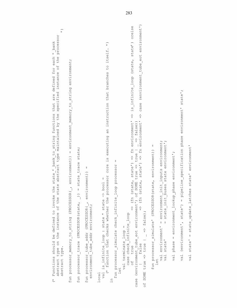
283
(* Functions should be defined to invoke the state_*_bank_to_string functions that are defined for each *_bank
abstract type on the instance of the state abstract type maintained by the specified instance of the processor
abstract type. *)
fun processor_memory_to_string (PROCESSOR(_, environment)) = environment_memory_to_string environment;
fun processor_trace (PROCESSOR(state, _)) = state_trace state;
fun processor_tube_addr (PROCESSOR(_, environment)) =
environment_tube_addr environment;
local
val is_infinite_loop : state * state -> bool =
(* function that checks whether the processor core is executing an instruction that branches to itself. *)
in
fun processor_simulate check_infinite_loop processor =
let
val terminate_loop =
case check_infinite_loop
of true => (fn (state, state') => fn environment' => is_infinite_loop (state, state’) orelse
case (environment_tube_eot environment') of SOME true => true | _ => false))
| false => (fn (state, state') => fn environment' => case (environment_tube_eot environment')
of SOME true => true | _ => false);
fun processor_simulate' (PROCESSOR(state, environment)) =
let
val environment' = environment_init_inputs environment;
val state' = state_init_buses state environment';
val phase = environment_lookup_phase environment';
val (environment', state') = pipeline_specification phase environment' state';
val state' = state_update_latches state' environment'
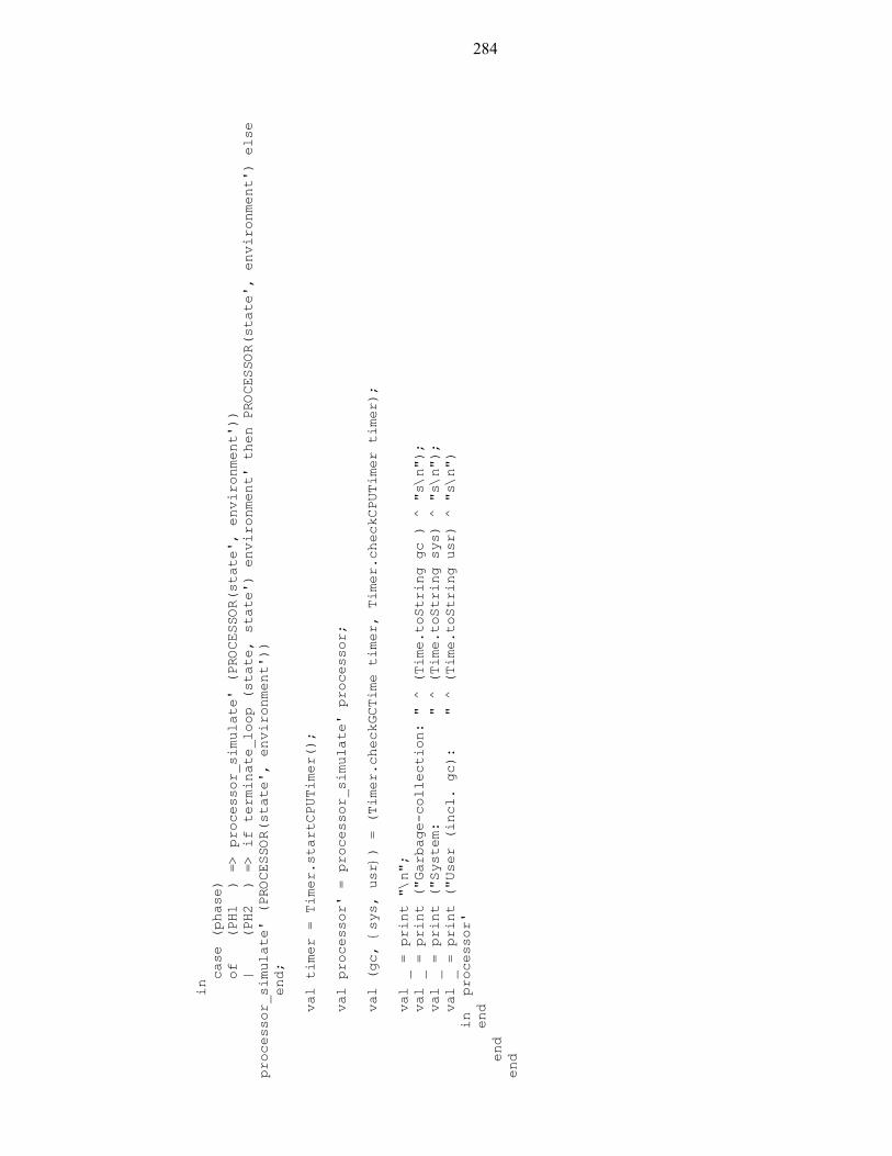
284
in
case (phase)
of (PH1 ) => processor_simulate' (PROCESSOR(state', environment'))
| (PH2 ) => if terminate_loop (state, state') environment' then PROCESSOR(state', environment') else
processor_simulate' (PROCESSOR(state', environment'))
end;
val timer = Timer.startCPUTimer();
val processor' = processor_simulate' processor;
val (gc, {sys, usr}) = (Timer.checkGCTime timer, Timer.checkCPUTimer timer);
val _ = print "\n";
val _ = print ("Garbage-collection: " ^ (Time.toString gc ) ^ "s\n");
val _ = print ("System: " ^ (Time.toString sys) ^ "s\n");
val _ = print ("User (incl. gc): " ^ (Time.toString usr) ^ "s\n")
in processor'
end
end
end