Embed Size (px)
Citation preview
MICRO SYNTHETIC APERTURE RADAR USING FM/CW
TECHNOLOGY
by
Ryan L. Smith
A thesis submitted to the faculty of
Brigham Young University
in partial fulfillment of the requirements for the degree of
Master of Science
Department of Electrical and Computer Engineering
Brigham Young University
December 2002

Copyright c© 2002 Ryan L. Smith
All Rights Reserved

BRIGHAM YOUNG UNIVERSITY
GRADUATE COMMITTEE APPROVAL
of a thesis submitted by
Ryan L. Smith
This thesis has been read by each member of the following graduate committee andby majority vote has been found to be satisfactory.
Date David V. Arnold, Chair
Date Michael A. Jensen
Date David G. Long

BRIGHAM YOUNG UNIVERSITY
As chair of the candidate’s graduate committee, I have read the thesis of Ryan L.Smith in its final form and have found that (1) its format, citations, and bibliograph-ical style are consistent and acceptable and fulfill university and department stylerequirements; (2) its illustrative materials including figures, tables, and charts are inplace; and (3) the final manuscript is satisfactory to the graduate committee and isready for submission to the university library.
Date David V. ArnoldChair, Graduate Committee
Accepted for the Department
A. Lee SwindlehurstGraduate Coordinator
Accepted for the College
Douglas M. ChabriesDean, College of Engineering and Technology
ABSTRACT
MICRO SYNTHETIC APERTURE RADAR USING FM/CW TECHNOLOGY
Ryan L. Smith
Department of Electrical and Computer Engineering
Master of Science
This work demonstrates a synthetic aperture radar (SAR) capable of gener-
ating high quality images using frequency modulated, continuous wave (FM/CW)
technology and it’s advantages over conventional SAR systems. A mathematical
analysis examines the range and azimuth compression of a single target and shows
that FM/CW based SAR produces compressed images. A 10 GHz prototype is de-
veloped using innovative coplanar techniques and a simple FM/CW signal generator.
The performance of the system matches the expected performance based upon the
analysis. The experimental and mathematical models support the conclusion that
FM/CW based SAR is capable of creating well-compressed imagery in both range
and azimuth.

ACKNOWLEDGMENTS
The work contained in this thesis is made possible by the contributions and
funding of the Canadian National Railway, National Aeronautic and Space Adminis-
tration, and the Brigham Young University College of Engineering. Thanks is given
to Don Crockett, Jeff Beard, and Jonathan Waite who contributed to development
of the FM/CW radar system and assisted me on several projects.
David Arnold who acted as my advisor and mentor provided me with an
early opportunity to learn engineering principles. I express my thanks to him for
believing in my abilities and making challenging research opportunities available to
students. He also helped me strengthen areas of my skills that were lacking and
helped me achieve the educational goals that I had set. Michael Jensen assisted in
this research with his expertise in high frequency circuit simulation and design. Some
of the simulations used in this work are based upon work assignments he gave in class
course work.
I am grateful to my parents for their encouragement to gain a higher education
and the example of work and endurance. My father’s interest in science and its
application initiated a desire in me that feeds the joy I find in engineering. A special
thanks goes to my wife Michelle and daughter Hannah for their encouragement and
support in completing this thesis. They were patient during many unexpected delays,
allowing me to focus on the development of this thesis.
Contents
Acknowledgments vi
List of Tables xi
List of Figures xv
1 Introduction 1
1.1 Purpose . . . . . . . . . . . . . . . . . . . . . . . . . . . . . . . . . . 1
1.2 Contributions of this Work . . . . . . . . . . . . . . . . . . . . . . . . 2
1.3 Outline . . . . . . . . . . . . . . . . . . . . . . . . . . . . . . . . . . . 3
2 SAR Background 5
2.1 Microwave Sensors . . . . . . . . . . . . . . . . . . . . . . . . . . . . 5
2.2 Current SAR Systems and Applications . . . . . . . . . . . . . . . . . 8
2.2.1 SIR-C/X-SAR . . . . . . . . . . . . . . . . . . . . . . . . . . . 8
2.2.2 NASA’s AIRSAR . . . . . . . . . . . . . . . . . . . . . . . . . 11
2.2.3 Intermap’s STAR-3i . . . . . . . . . . . . . . . . . . . . . . . 13
2.2.4 BYU’s SAR Program . . . . . . . . . . . . . . . . . . . . . . . 16
2.2.5 Basis for the BYµSAR . . . . . . . . . . . . . . . . . . . . . . 20
3 FM/CW SAR Techniques 23
3.1 FM/CW Range Detection and Resolution . . . . . . . . . . . . . . . 23
3.1.1 Range Detection . . . . . . . . . . . . . . . . . . . . . . . . . 23
3.1.2 Range Resolution and Processing Gain . . . . . . . . . . . . . 25
3.2 SAR Geometry . . . . . . . . . . . . . . . . . . . . . . . . . . . . . . 28
3.3 Illustrated SAR Compression . . . . . . . . . . . . . . . . . . . . . . 28
vii

3.3.1 Pulsed FM SAR . . . . . . . . . . . . . . . . . . . . . . . . . . 29
3.3.2 FM/CW SAR . . . . . . . . . . . . . . . . . . . . . . . . . . . 32
3.4 Range Compression Techniques . . . . . . . . . . . . . . . . . . . . . 33
3.4.1 FM/CW Range Compression . . . . . . . . . . . . . . . . . . 33
3.4.2 Pulsed FM Range Compression . . . . . . . . . . . . . . . . . 36
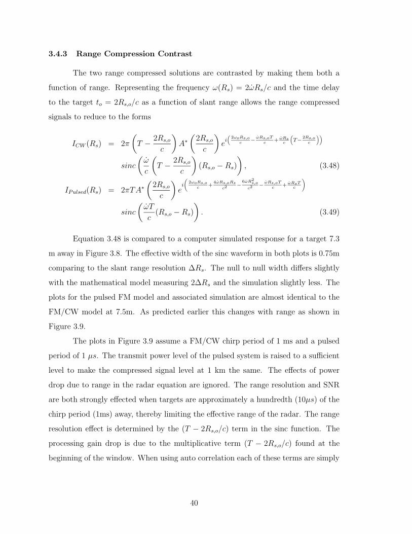
3.4.3 Range Compression Contrast . . . . . . . . . . . . . . . . . . 40
3.5 Azimuth Compression . . . . . . . . . . . . . . . . . . . . . . . . . . 41
3.5.1 Derivation . . . . . . . . . . . . . . . . . . . . . . . . . . . . . 41
3.5.2 FM/CW Phase Error Analysis . . . . . . . . . . . . . . . . . . 45
3.6 FM/CW Limitations and Optimization . . . . . . . . . . . . . . . . . 52
4 BYµSAR System Design 55
4.1 BYµSAR Specifications . . . . . . . . . . . . . . . . . . . . . . . . . . 55
4.1.1 Airborne System Specifications . . . . . . . . . . . . . . . . . 55
4.1.2 Track System Specifications . . . . . . . . . . . . . . . . . . . 58
4.1.3 Block Diagram . . . . . . . . . . . . . . . . . . . . . . . . . . 58
4.2 Transmitter . . . . . . . . . . . . . . . . . . . . . . . . . . . . . . . . 61
4.2.1 LFM Generation . . . . . . . . . . . . . . . . . . . . . . . . . 61
4.2.2 RF Module . . . . . . . . . . . . . . . . . . . . . . . . . . . . 63
4.2.3 RF Driver Module . . . . . . . . . . . . . . . . . . . . . . . . 65
4.2.4 Algorithms and Control Code . . . . . . . . . . . . . . . . . . 69
4.3 Low Noise Receiver . . . . . . . . . . . . . . . . . . . . . . . . . . . . 71
4.3.1 Low Noise Amplifier . . . . . . . . . . . . . . . . . . . . . . . 72
4.3.2 RF Mixer Module . . . . . . . . . . . . . . . . . . . . . . . . . 75
4.3.3 IF Gain Module . . . . . . . . . . . . . . . . . . . . . . . . . . 76
4.4 System Assembly . . . . . . . . . . . . . . . . . . . . . . . . . . . . . 77
4.5 Signal to Noise Analysis . . . . . . . . . . . . . . . . . . . . . . . . . 79
4.5.1 The Radar Equation . . . . . . . . . . . . . . . . . . . . . . . 81
4.5.2 Radiometric Noise . . . . . . . . . . . . . . . . . . . . . . . . 84
4.5.3 Thermal Noise . . . . . . . . . . . . . . . . . . . . . . . . . . 86
viii
4.5.4 SNR Calculations . . . . . . . . . . . . . . . . . . . . . . . . . 88
5 BYµSAR System Tests 91
5.1 Bench Tests . . . . . . . . . . . . . . . . . . . . . . . . . . . . . . . . 91
5.1.1 Phase Counter . . . . . . . . . . . . . . . . . . . . . . . . . . 91
5.1.2 Impulse Response . . . . . . . . . . . . . . . . . . . . . . . . . 92
5.1.3 Transmitter Spectral Output . . . . . . . . . . . . . . . . . . . 94
5.2 Inverse SAR of Corner Reflector . . . . . . . . . . . . . . . . . . . . . 94
5.3 Imaging using Track Platform . . . . . . . . . . . . . . . . . . . . . . 97
6 Conclusion 103
6.1 Summary . . . . . . . . . . . . . . . . . . . . . . . . . . . . . . . . . 103
6.2 Future Work . . . . . . . . . . . . . . . . . . . . . . . . . . . . . . . . 104
6.3 Contributions . . . . . . . . . . . . . . . . . . . . . . . . . . . . . . . 105
A Channelized Coplanar Waveguide Technology 107
A.1 Coplanar’s Benefits . . . . . . . . . . . . . . . . . . . . . . . . . . . . 107
A.2 50Ω Transmission Line . . . . . . . . . . . . . . . . . . . . . . . . . . 108
A.3 DC Isolation and Cavity Effects . . . . . . . . . . . . . . . . . . . . . 110
A.4 CCPW Elements . . . . . . . . . . . . . . . . . . . . . . . . . . . . . 111
A.5 Prototypes and Developing . . . . . . . . . . . . . . . . . . . . . . . . 113
B SAR Imaging Functions 117
C SAR Visual Basic Code for Instrument Control 121
D PicBasicPro Code for Transmitter Module 129
E PicBasicPro Code for Receiver Module 137
F PECL Design Overview 141
F.1 ECL Basic Gate . . . . . . . . . . . . . . . . . . . . . . . . . . . . . . 141
F.2 Positive Emitter Coupled Logic . . . . . . . . . . . . . . . . . . . . . 141
F.3 Termination of Transmission Lines and Interconnects . . . . . . . . . 142
ix

Bibliography 149
x

List of Tables
2.1 Comparison of Six SAR Systems with the BYµSAR. . . . . . . . . . 22
4.1 BYµSAR Airborne Parameters . . . . . . . . . . . . . . . . . . . . . 57
4.2 BYµSAR Track Parameters . . . . . . . . . . . . . . . . . . . . . . . 59
4.3 LNA Interdigital Dimensions . . . . . . . . . . . . . . . . . . . . . . . 76
5.1 RF Module Output Spectrum . . . . . . . . . . . . . . . . . . . . . . 95
A.1 Tangential Line Coupling in Coplanar . . . . . . . . . . . . . . . . . . 113
F.1 ECL to PECL Voltage Level Conversion . . . . . . . . . . . . . . . . 142
xi

xii

List of Figures
2.1 Radiometer Image of Southeast Asia . . . . . . . . . . . . . . . . . . 6
2.2 SIR-C/X-SAR Aboard the Space Shuttle . . . . . . . . . . . . . . . . 8
2.3 SIR-C Image of Salt Lake City . . . . . . . . . . . . . . . . . . . . . . 9
2.4 X-SAR Image enhancement of the Rocky Mountains . . . . . . . . . . 10
2.5 AIRSAR’s DC-8 Aircraft and Equipment Racks . . . . . . . . . . . . 11
2.6 AIRSAR Image of Canadian Farm Land . . . . . . . . . . . . . . . . 12
2.7 STAR-3i Integrated into a Learjet 36 . . . . . . . . . . . . . . . . . . 14
2.8 STAR-3i Created DEMs near Denver, Colorado . . . . . . . . . . . . 15
2.9 Truck platform used to deploy BYUSAR . . . . . . . . . . . . . . . . 16
2.10 BYU SAR Image near University Avenue, Provo, Utah . . . . . . . . 17
2.11 YINSAR uncovers an archeological site in Israel . . . . . . . . . . . . 18
2.12 YINSAR’s Aircraft and Hardware . . . . . . . . . . . . . . . . . . . . 19
2.13 Image of BYU Campus by YINSAR . . . . . . . . . . . . . . . . . . . 20
3.1 The Real Part of the Exponential Chirp m(t). . . . . . . . . . . . . . 24
3.2 How a Chirp is Used to Measure Distance . . . . . . . . . . . . . . . 26
3.3 Rayleigh Resolution and the Sinc Function . . . . . . . . . . . . . . . 27
3.4 SAR Geometry . . . . . . . . . . . . . . . . . . . . . . . . . . . . . . 29
3.5 Illustrated Range Compression . . . . . . . . . . . . . . . . . . . . . . 30
3.6 Illustrated Azimuth Compression . . . . . . . . . . . . . . . . . . . . 31
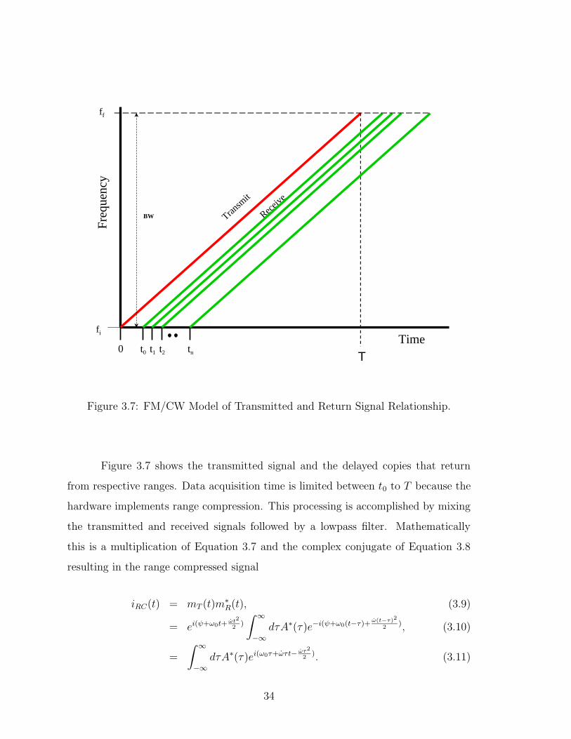
3.7 FM/CW Model of Transmitted and Return Signal Relationship. . . . 34
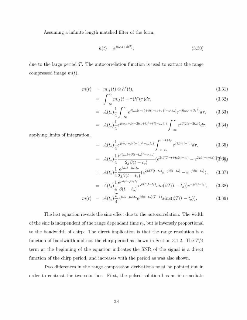
3.8 Mathematical and Simulated FM/CW Range Compression . . . . . . 41
3.9 Mathematical Model Showing Both SNR and Resolution Degradation 42
3.10 Distance Relationship of Moving Platform and a Single Target. . . . . 43
3.11 Range Walk due to Extended FM/CW Chirp Period . . . . . . . . . 50
xiii
3.12 Compressed Azimuth Response for FM/CW . . . . . . . . . . . . . . 52
4.1 Maximum and Minimum Range . . . . . . . . . . . . . . . . . . . . . 56
4.2 Range resolution is related to slant range resolution, range, and elevation. 56
4.3 Simplified Block Diagram of SAR System. . . . . . . . . . . . . . . . 60
4.4 VCO Nonlinearities . . . . . . . . . . . . . . . . . . . . . . . . . . . . 62
4.5 Block Diagram of Transmitter Architecture. . . . . . . . . . . . . . . 63
4.6 Transmitter Module Schematic. . . . . . . . . . . . . . . . . . . . . . 64
4.7 Transmitter Module . . . . . . . . . . . . . . . . . . . . . . . . . . . . 65
4.8 Main board Schematic Including Transmitter Driver. . . . . . . . . . 66
4.9 Driver Board without Modules. . . . . . . . . . . . . . . . . . . . . . 67
4.10 Frequency Profile of Transmit Signal . . . . . . . . . . . . . . . . . . 68
4.11 Transmitter Calibration Algorithm . . . . . . . . . . . . . . . . . . . 71
4.12 Visual Basic Graphical User Interface . . . . . . . . . . . . . . . . . . 72
4.13 Biasing Network for Gate and Drain. . . . . . . . . . . . . . . . . . . 73
4.14 NE329S01 Γs Biased at 2 Volts and 10 mA . . . . . . . . . . . . . . . 74
4.15 NE329S01 Γs Biased at 3 Volts and 20 mA . . . . . . . . . . . . . . . 75
4.16 Matching Network and Transistor Setup for a 50 dB Low Noise Amplifier. 76
4.17 ADS Simulation of LNA. . . . . . . . . . . . . . . . . . . . . . . . . . 77
4.18 ADS Simulation Results for LNA. . . . . . . . . . . . . . . . . . . . . 77
4.19 Measurements of 10 GHz Low Noise Amplifier with 50 dB of Gain. . 78
4.20 10 GHz Low Noise Amplifier with 50 dB of Gain. . . . . . . . . . . . 78
4.21 HMC220S08 Mixer in Housing. . . . . . . . . . . . . . . . . . . . . . 79
4.22 IF Filter and Amplification Module. . . . . . . . . . . . . . . . . . . . 79
4.23 Bottom View of RF Subassembly . . . . . . . . . . . . . . . . . . . . 80
4.24 Top View of RF Subassembly . . . . . . . . . . . . . . . . . . . . . . 81
4.25 Complete SAR System with all Modules in Place. . . . . . . . . . . . 82
4.26 Radiometric Noise for Radar . . . . . . . . . . . . . . . . . . . . . . . 84
4.27 Typical RF Receiver’s Noise Figure and Gain . . . . . . . . . . . . . 87
5.1 Setup for verifying the accuracy of the SAR’s phase counting circuit. 92
5.2 Measurement of Linearity of Phase Counter . . . . . . . . . . . . . . 92
xiv

5.3 Test Setup for the Impulse Response. . . . . . . . . . . . . . . . . . . 93
5.4 Time and Frequency Domain Responses for the Impulse Response Test 94
5.5 BYµSAR is Stationary While it Images a Moving Corner Reflector. . 95
5.6 Azimuthal Response from a Moving Corner Reflector . . . . . . . . . 96
5.7 Azimuth and Range Resolution . . . . . . . . . . . . . . . . . . . . . 96
5.8 Range and Azimuth Compressed Image of a Corner Reflector . . . . . 97
5.9 BYµSAR Imaging the Fletcher Building and Wilkinson Center . . . . 98
5.10 Radar Acquisition Setup for Imaging . . . . . . . . . . . . . . . . . . 99
5.11 SAR Image of Fletcher Building Contrasted with Photographs . . . . 100
5.12 Image Taken of the Fletcher and Clyde Buildings from Airborne YINSAR101
A.1 Static solution of microstrip and coplanar technologies . . . . . . . . 108
A.2 Test fixture Used to Analyze Coplanar Circuits . . . . . . . . . . . . 109
A.3 Layout of Simulation and Board to Case Transition . . . . . . . . . . 110
A.4 ADS Momentum Simulation Results of a 50Ω Line. . . . . . . . . . . 111
A.5 Board Used to Analyze Isolation in Coplanar . . . . . . . . . . . . . . 112
A.6 A 5 Port Hybrid Ring in Coplanar . . . . . . . . . . . . . . . . . . . 114
A.7 Fundamental Circuit Elements in Coplanar . . . . . . . . . . . . . . . 115
A.8 Staggered Interdigital Capacitor . . . . . . . . . . . . . . . . . . . . . 115
F.1 An AC Signal Coupled to an ECL Device. . . . . . . . . . . . . . . . 143
xv
Chapter 1
Introduction
1.1 Purpose
Synthetic Aperture Radar (SAR) is recognized for its ability to construct high-
resolution images. Current strip-map SAR systems are complex in design because
they use pulsed FM waveforms to produce the radar signals. FM/CW is a technique
used in many radar systems to achieve high pulse compression and large processing
gains. FM/CW has not been validated as a viable SAR foundation for remote sensing
applications. The work presented here shows that a SAR is capable of generating
high quality imagery devoid of serious defects using FM/CW technology. The proof
is based upon a mathematical analysis and the results of a prototype FM/CW based
SAR system.
Six SARs are described along with their platforms and uses in order to show
the significance of the novel SAR system described in this work. Six SAR systems
are described ranging from the orbital SIR-C/X-SAR aboard the space shuttle to
a system that is used in a Cessna airplane. Their uses range from archeology to
platetectonics by providing information that is not easily obtained by other means.
The Brigham Young micro SAR (BYµSAR) finds a niche by providing a compact,
affordable, high resolution SAR with the aid of FM/CW technology.
Traditional methods of generating radar signals are contrasted with this use
of FM/CW to show that a number of key benefits are achieved using the latter.
The comparison is first carried out in an illustrative manner followed by a detailed
mathematical analysis. The analysis shows the range and azimuth compression for
1
both types of systems and concludes with a phase error analysis. The phase analysis
shows that FM/CW based SAR does not introduce significant errors in the azimuthal
phase response and thus allows excellent azimuth compression.
A short guide is given on how to select the optimum parameters for a FM/CW-
based SAR using key equations derived in the analysis section 3.5.2. A prototype SAR
based on the earlier developments is then shown. The system is designed and built
using coplanar technology which is covered in the Appendix. The SAR performance
is measured by plotting the range and azimuth compressed response of a single corner
reflector. Its abilities are further illustrated in an image acquired of a building. These
results show that FM/CW technology is able to create high-quality SAR imagery that
is well-compressed in azimuth and range. The BYµSAR is therefore well suited to
many applications that are not currently feasible in traditional SAR systems.
1.2 Contributions of this Work
The work in this thesis introduces a sensor and an analytic solution to a
new technique for SAR imaging. The analytic solution derived represents the range
compressed signal in the frequency domain. It shows that FM/CW SAR introduces
no azimuth phase errors within limitations, but adds a linear shift to range walk
as shown. A simple LFM signal generator is designed and built that obtains good
linearity and fair frequency stability.
Techniques are developed to design and make innovative coplanar circuits using
relatively inexpensive equipment. A high gain, low noise amplifier is achieved using
a low cost printed circuit board substrate and this gives confidence for the design of
other technical building blocks of microwave circuits. The development of a modular
style microwave design is initiated where parts such as the driver circuit could be
reused in other designs helping to eliminate unnecessary design cost and effort.
2
1.3 Outline
This thesis is developed as follows:
Chapter 2 gives a background to SAR by describing microwave sensors and
explaining their benefits. Six different SAR systems are analyzed by looking at their
application and the images they produced.
Chapter 3 covers FM/CW range detection and resolution followed by SAR
geometry. An illustrative approach is taken to FM/CW SAR compared to pulsed
FM SAR before it is mathematically contrasted. The effects that FM/CW has on
SAR imaging is presented along with a guide for optimum system configuration.
Chapter 4 specifies the parameters for a BYµSAR prototype design. It then
covers the design and construction of the transmitter, receiver, and other system
components. A detailed signal-to-noise ratio analysis covers radiometric and thermal
noise sources.
Chapter 5 identifies several bench tests performed on the BYµSAR system and
provides the results. The radar resolution is then measured using a moving corner
reflector. Data is then taken by the SAR system and an image of a building is formed
using SAR processing. This image is then compared to photographs.
Chapter 6 is the conclusion containing a summary of the thesis, a outline of
proposed future enhancements, and a list the contributions made.
Appendix A covers a relatively new technology of channelized coplanar waveg-
uides used to build microwave circuits. Here its benefits and abilities to realize key
elements with ease are examined. The board manufacturing system is also described
along with issues encounter in the board manufacturing process.
Appendix B includes the functions used in the processing of the SAR images.
Appendix C shows the Visual Basic code used for instrument control.
Appendix D shows the PicBasicPro code for the microcontroller used in the
transmitter.
Appendix E shows the PicBasicPro code for the microcontroller used in the
receiver’s IF gain block.
3

Appendix F gives a brief overview and design help for Positive Emitter Coupled
Logic (PECL).
4
Chapter 2
SAR Background
This chapter gives a brief background of microwave sensors and provides the
motivation for the development of the BYµSAR. Six SAR systems are described
ranging from an orbital sensor aboard the space shuttle to units mounted in small
aircraft. In addition, numerous examples of current SAR imagery products are shown
in figures that graphically illustrate their usefulness. The advantages of a miniature
system like BYµSAR are then discussed in light of the current systems now in use,
and a comparison follows in a table.
2.1 Microwave Sensors
SAR has many features that give it an advantage over other sensors for imag-
ing. SAR is selected for its ability to penetrate the atmosphere and ground, precisely
measure range, and provide high resolution images with height detection.
Images are able to quickly communicate a large amount of information that
is otherwise obscure and difficult to communicate. Decisions are made based on the
information that is available and accessible. The eye and mind are trained to look
for and focus on contrasts in order to analyze a given view. Rich optical images are
formed by bordering colors and shades that produce sharp edges and high contrasts,
and these are prevalent in man-made and natural structures. Then why use radar
when optics can provide an image that is full of detail and familiar to the observer?
Microwaves have three key advantages over optics. First, they can penetrate
rain, smoke and dust clouds; second, they are not dependent on the sun for illumina-
tion; and third, they are able to penetrate through vegetation and soils. The ability of
5
radar signals to penetrate is a linear function of wavelength, where longer wavelength
signals penetrate deeper. Large contrasts are seen in radar images between objects
that reflect energy well and materials that do not. Microwave frequencies range from
300 MHz to 100 GHz corresponding to wavelengths of 1m to 3 mm respectively [1].
Himalayas
Gulf of Martaban
Sri Lanka
India
Gulf of Cambay
Mouth of the Ganges
Gulf of Thailand
Pakistan
Tibetan Plateau
Malaysia
Gulf of Tonkin
Taiwan
Philippines
Malaysia
Hong Kong
China
Vietnam
Afghanistan
Nepal
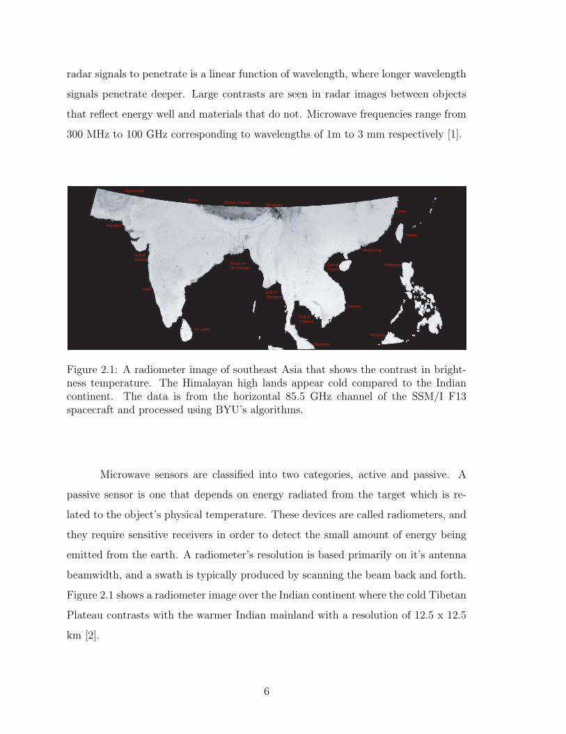
Figure 2.1: A radiometer image of southeast Asia that shows the contrast in bright-ness temperature. The Himalayan high lands appear cold compared to the Indiancontinent. The data is from the horizontal 85.5 GHz channel of the SSM/I F13spacecraft and processed using BYU’s algorithms.
Microwave sensors are classified into two categories, active and passive. A
passive sensor is one that depends on energy radiated from the target which is re-
lated to the object’s physical temperature. These devices are called radiometers, and
they require sensitive receivers in order to detect the small amount of energy being
emitted from the earth. A radiometer’s resolution is based primarily on it’s antenna
beamwidth, and a swath is typically produced by scanning the beam back and forth.
Figure 2.1 shows a radiometer image over the Indian continent where the cold Tibetan
Plateau contrasts with the warmer Indian mainland with a resolution of 12.5 x 12.5
km [2].
6
The main feature of a radiometric image is the contrast of the brightness
temperature as a product of the physical temperature and emissivity. Emissivity is
the relation of brightness temperature to the physical temperature, with its value
ranging from zero to one. Metal objects have a emissivity of zero and appear very
dark where land surfaces vary from 0.3 to 0.7. Ocean and lakes have a low emissivity
and thus appear much colder than land. Dark spots in the image indicate sites of
urban centers and developed areas.
An active sensor transmits energy that reflects off targets in a scene and is then
received by a sensor. The transmit and receive signals are compared using processing
techniques that extract effects produced by individual targets known as a coherent
processing. Active sensors are also called Radar (Radio Detection and Ranging)[1].
Radar is commonly thought of as a circular green display that has a scan beam
rotating around the center, displaying a target as a bright dot when detected. This
is known as the plan-position indicator because it is able to measure the distance to
an object with precision.
Radar signals can be modified or filtered into a format that displays the in-
formation of interest with an appropriate amount of contrast. Doppler radar used in
weather forecasting uses bright colored maps to reveal storm systems as they move
over a region. Radar does not differentiate the color spectrum like an optical cam-
era; rather, it perceives electromagnetic properties of physical objects as well as the
geometric shape and orientation of targets[1]. For example, metal objects reflect elec-
tromagnetic (EM) waves much like a mirror reflects light. Other materials absorb
most of the incoming EM energy similar to the way black objects absorb optical
energy.
SAR is an active sensor that uses multiple illuminations to produce a high
resolution image. Signals are processed to get desired information such as range,
height, and the scene’s electromagnetic properties. Interferometric SAR is a system
that has multiple receive antennas that are separated vertically on the platform. This
geometrical relationship allows the measurement of relative heights, thereby enabling
terrain mapping [3]. SAR systems are commonly used in military applications to
7
perform target recognition, reconnaissance, damage assessment, and border watch.
This work focuses on non-military systems and their applications.
2.2 Current SAR Systems and Applications
Six systems are contrasted with key features of frequency, resolution, platform
velocity, swath width, elevation, transmit and system power, imaging rate, in-flight
or post-flight processing, weight, and cost. Applications include terrain mapping,
archeology, agricultural and urban planning, platetectonics, and oceanography. The
six systems that will be described are: SIR-C/X-SAR, NASA’s AIR-SAR, Intermap’s
STAR-3i, and BYU’s BYU-SAR, YSAR, and YINSAR. The BYµSAR is then con-
trasted with these six systems showing that it provides a valuable and complementary
source of SAR imagery.
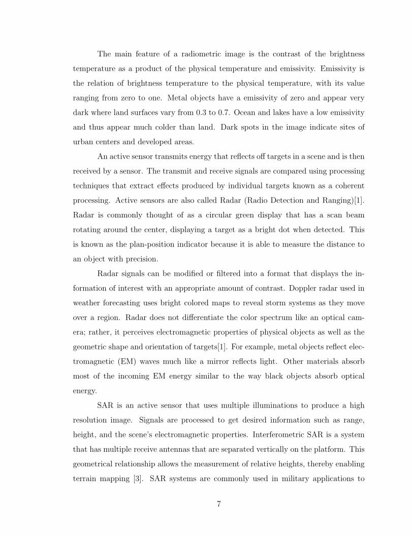
2.2.1 SIR-C/X-SAR
Figure 2.2: SIR-C/X-SAR aboard the space shuttle at an orbit altitude of 225 km.Courtesy of NASA/JPL.
8
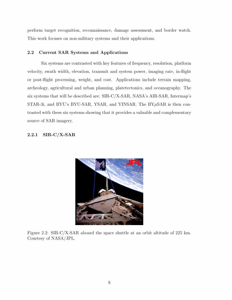
This section looks at the SIR-C/X-SAR system and then at a diverse terrain
map over Salt Lake City, Utah that was created using data collected by SIR-C shown
in Figure 2.3. Figure 2.4 is shown of the Rocky Mountains in Montana showing the
usefulness of SAR in geology.
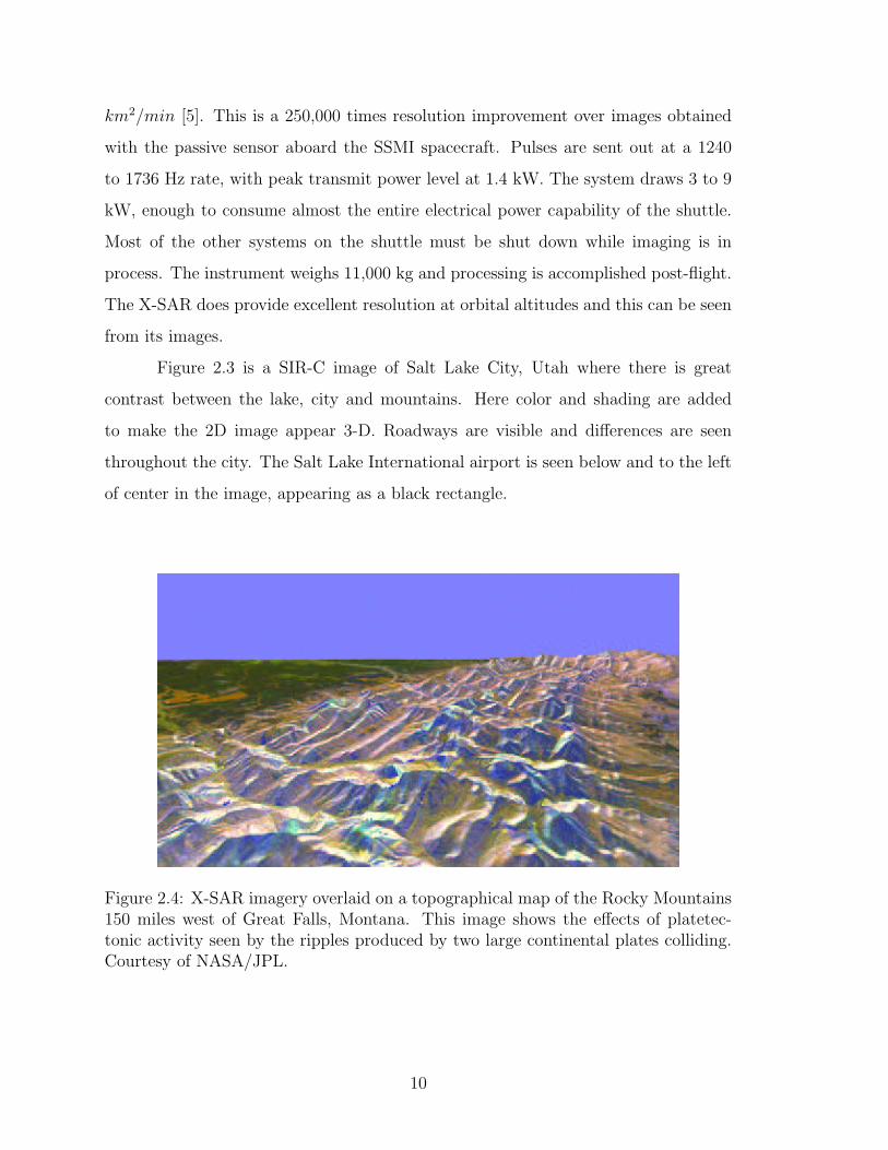
Figure 2.3: SIR-C image of Salt Lake City, Utah showing the lake, mountains, andcity. Courtesy of NASA/JPL.
X-SAR is a 9.6 GHz system developed by the German and Italian Aerospace
Agencies for use on the space shuttle as seen in Figure 2.2. SIR-C was developed by
the United States and operated in the L and C bands. Both SAR systems operate
simultaneously aboard the space shuttle. Their primary purpose is imaging vegetation
variation, oceans, snow, ice and geological activity [4]. The space shuttle orbits 225
km above the earth while imaging with X-SAR, producing a 20 to 70 km swath on
the surface of the earth with a 25 x 25 m resolution and an imaging rate of 17,000
9
km2/min [5]. This is a 250,000 times resolution improvement over images obtained
with the passive sensor aboard the SSMI spacecraft. Pulses are sent out at a 1240
to 1736 Hz rate, with peak transmit power level at 1.4 kW. The system draws 3 to 9
kW, enough to consume almost the entire electrical power capability of the shuttle.
Most of the other systems on the shuttle must be shut down while imaging is in
process. The instrument weighs 11,000 kg and processing is accomplished post-flight.
The X-SAR does provide excellent resolution at orbital altitudes and this can be seen
from its images.
Figure 2.3 is a SIR-C image of Salt Lake City, Utah where there is great
contrast between the lake, city and mountains. Here color and shading are added
to make the 2D image appear 3-D. Roadways are visible and differences are seen
throughout the city. The Salt Lake International airport is seen below and to the left
of center in the image, appearing as a black rectangle.
Figure 2.4: X-SAR imagery overlaid on a topographical map of the Rocky Mountains150 miles west of Great Falls, Montana. This image shows the effects of platetec-tonic activity seen by the ripples produced by two large continental plates colliding.Courtesy of NASA/JPL.
10
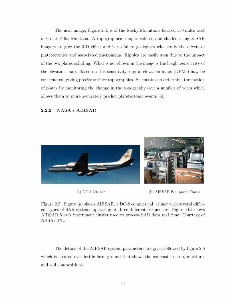
The next image, Figure 2.4, is of the Rocky Mountains located 150 miles west
of Great Falls, Montana. A topographical map is colored and shaded using X-SAR
imagery to give the 3-D effect and is useful to geologists who study the effects of
platetectonics and associated phenomena. Ripples are easily seen due to the impact
of the two plates colliding. What is not shown in the image is the height sensitivity of
the elevation map. Based on this sensitivity, digital elevation maps (DEMs) may be
constructed, giving precise surface topographies. Scientists can determine the motion
of plates by monitoring the change in the topography over a number of years which
allows them to more accurately predict platetectonic events [6].
2.2.2 NASA’s AIRSAR
(a) DC-8 Jetliner (b) AIRSAR Equipment Racks
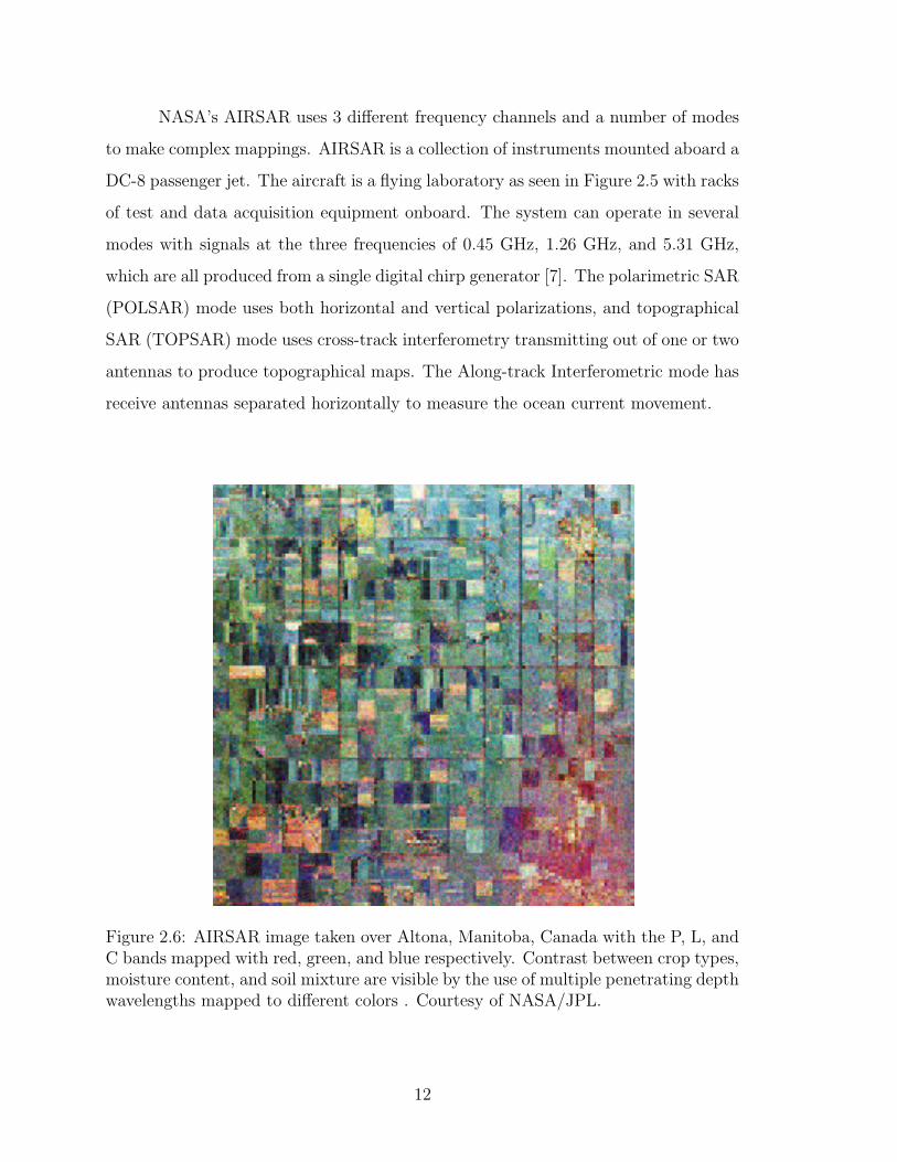
Figure 2.5: Figure (a) shows AIRSAR, a DC-8 commercial jetliner with several differ-ent types of SAR systems operating at three different frequencies. Figure (b) showsAIRSAR 5 rack instrument cluster used to process SAR data real time. Courtesy ofNASA/JPL.
The details of the AIRSAR system parameters are given followed by figure 2.6
which is created over fertile farm ground that shows the contrast in crop, moisture,
and soil compositions.
11
NASA’s AIRSAR uses 3 different frequency channels and a number of modes
to make complex mappings. AIRSAR is a collection of instruments mounted aboard a
DC-8 passenger jet. The aircraft is a flying laboratory as seen in Figure 2.5 with racks
of test and data acquisition equipment onboard. The system can operate in several
modes with signals at the three frequencies of 0.45 GHz, 1.26 GHz, and 5.31 GHz,
which are all produced from a single digital chirp generator [7]. The polarimetric SAR
(POLSAR) mode uses both horizontal and vertical polarizations, and topographical
SAR (TOPSAR) mode uses cross-track interferometry transmitting out of one or two
antennas to produce topographical maps. The Along-track Interferometric mode has
receive antennas separated horizontally to measure the ocean current movement.
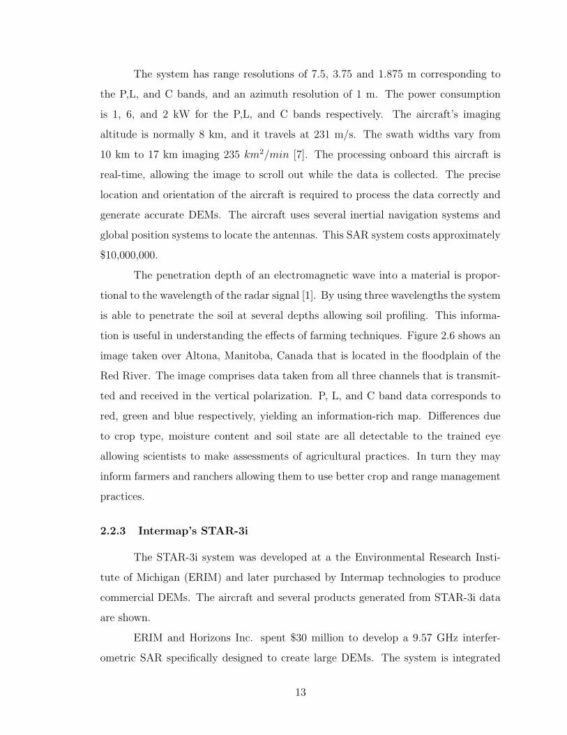
Figure 2.6: AIRSAR image taken over Altona, Manitoba, Canada with the P, L, andC bands mapped with red, green, and blue respectively. Contrast between crop types,moisture content, and soil mixture are visible by the use of multiple penetrating depthwavelengths mapped to different colors . Courtesy of NASA/JPL.
12
The system has range resolutions of 7.5, 3.75 and 1.875 m corresponding to
the P,L, and C bands, and an azimuth resolution of 1 m. The power consumption
is 1, 6, and 2 kW for the P,L, and C bands respectively. The aircraft’s imaging
altitude is normally 8 km, and it travels at 231 m/s. The swath widths vary from
10 km to 17 km imaging 235 km2/min [7]. The processing onboard this aircraft is
real-time, allowing the image to scroll out while the data is collected. The precise
location and orientation of the aircraft is required to process the data correctly and
generate accurate DEMs. The aircraft uses several inertial navigation systems and
global position systems to locate the antennas. This SAR system costs approximately
$10,000,000.
The penetration depth of an electromagnetic wave into a material is propor-
tional to the wavelength of the radar signal [1]. By using three wavelengths the system
is able to penetrate the soil at several depths allowing soil profiling. This informa-
tion is useful in understanding the effects of farming techniques. Figure 2.6 shows an
image taken over Altona, Manitoba, Canada that is located in the floodplain of the
Red River. The image comprises data taken from all three channels that is transmit-
ted and received in the vertical polarization. P, L, and C band data corresponds to
red, green and blue respectively, yielding an information-rich map. Differences due
to crop type, moisture content and soil state are all detectable to the trained eye
allowing scientists to make assessments of agricultural practices. In turn they may
inform farmers and ranchers allowing them to use better crop and range management
practices.
2.2.3 Intermap’s STAR-3i
The STAR-3i system was developed at a the Environmental Research Insti-
tute of Michigan (ERIM) and later purchased by Intermap technologies to produce
commercial DEMs. The aircraft and several products generated from STAR-3i data
are shown.
ERIM and Horizons Inc. spent $30 million to develop a 9.57 GHz interfer-
ometric SAR specifically designed to create large DEMs. The system is integrated
13
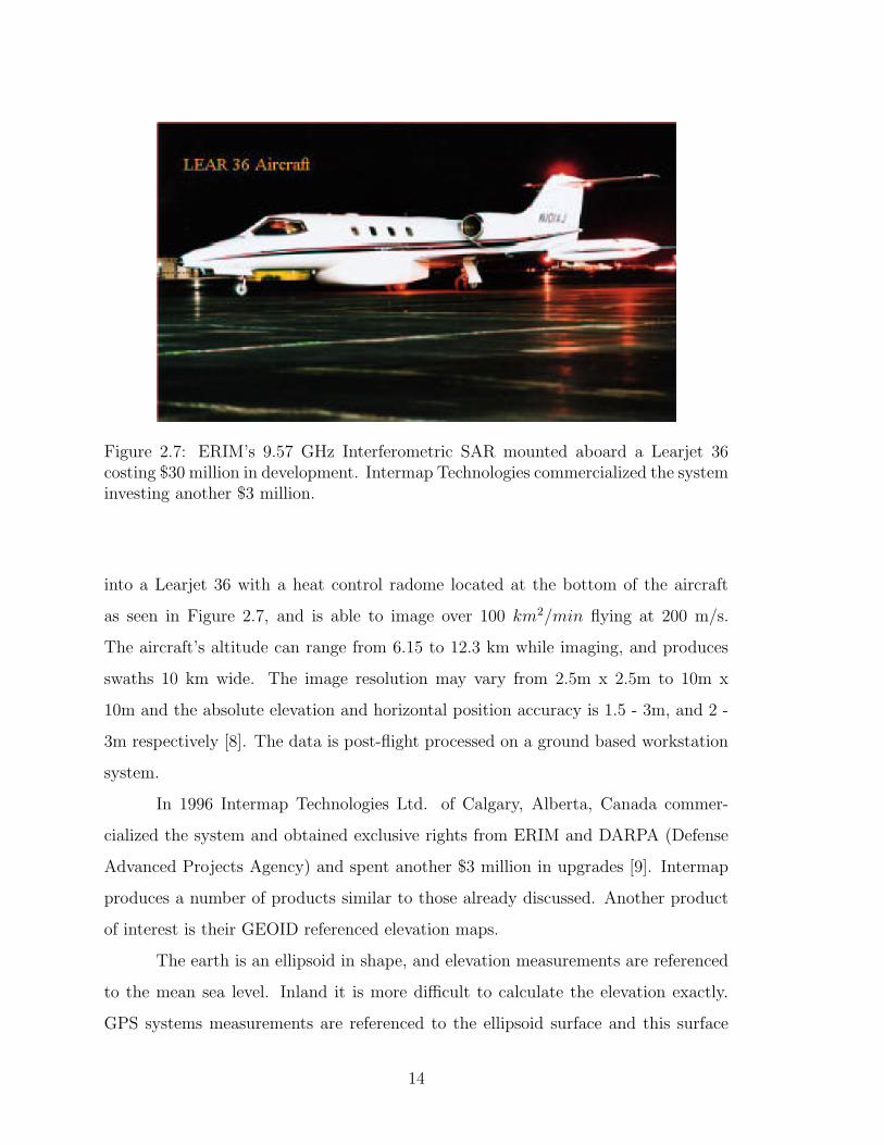
Figure 2.7: ERIM’s 9.57 GHz Interferometric SAR mounted aboard a Learjet 36costing $30 million in development. Intermap Technologies commercialized the systeminvesting another $3 million.
into a Learjet 36 with a heat control radome located at the bottom of the aircraft
as seen in Figure 2.7, and is able to image over 100 km2/min flying at 200 m/s.
The aircraft’s altitude can range from 6.15 to 12.3 km while imaging, and produces
swaths 10 km wide. The image resolution may vary from 2.5m x 2.5m to 10m x
10m and the absolute elevation and horizontal position accuracy is 1.5 - 3m, and 2 -
3m respectively [8]. The data is post-flight processed on a ground based workstation
system.
In 1996 Intermap Technologies Ltd. of Calgary, Alberta, Canada commer-
cialized the system and obtained exclusive rights from ERIM and DARPA (Defense
Advanced Projects Agency) and spent another $3 million in upgrades [9]. Intermap
produces a number of products similar to those already discussed. Another product
of interest is their GEOID referenced elevation maps.
The earth is an ellipsoid in shape, and elevation measurements are referenced
to the mean sea level. Inland it is more difficult to calculate the elevation exactly.
GPS systems measurements are referenced to the ellipsoid surface and this surface
14
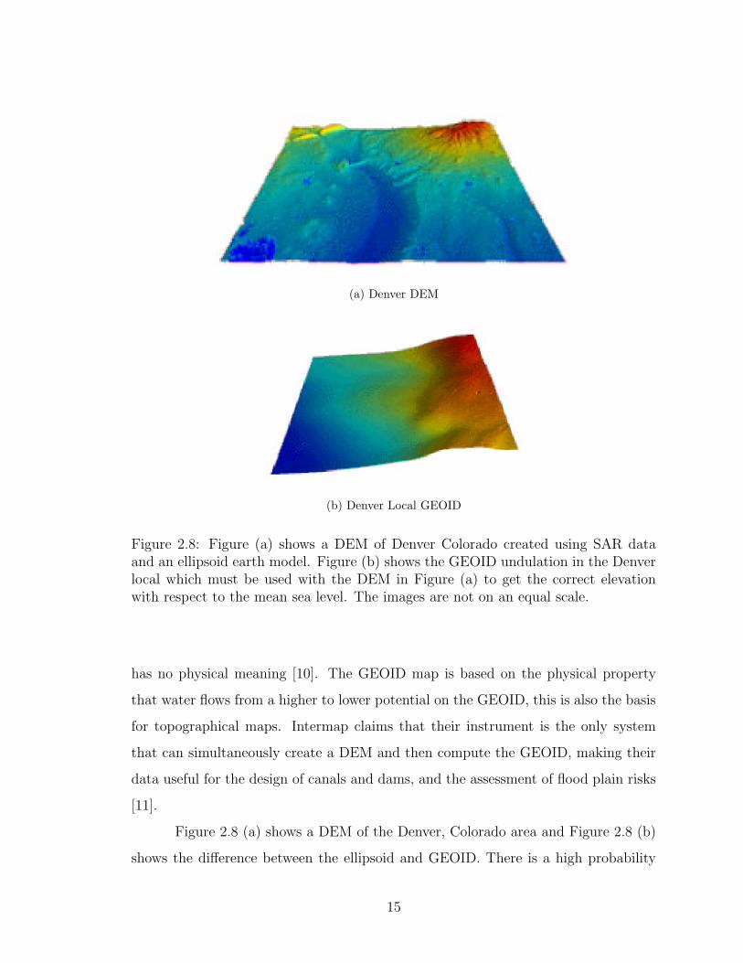
(a) Denver DEM
(b) Denver Local GEOID
Figure 2.8: Figure (a) shows a DEM of Denver Colorado created using SAR dataand an ellipsoid earth model. Figure (b) shows the GEOID undulation in the Denverlocal which must be used with the DEM in Figure (a) to get the correct elevationwith respect to the mean sea level. The images are not on an equal scale.
has no physical meaning [10]. The GEOID map is based on the physical property
that water flows from a higher to lower potential on the GEOID, this is also the basis
for topographical maps. Intermap claims that their instrument is the only system
that can simultaneously create a DEM and then compute the GEOID, making their
data useful for the design of canals and dams, and the assessment of flood plain risks
[11].
Figure 2.8 (a) shows a DEM of the Denver, Colorado area and Figure 2.8 (b)
shows the difference between the ellipsoid and GEOID. There is a high probability
15
that water would not flow in the direction intended if a canal were built in this area
only using GPS measurements. Quick feasibility studies can be carried out for various
hydro projects by the use of airborne SAR and its associated byproducts. Intermap
plans to map the entire United States in the next three years [11].
2.2.4 BYU’s SAR Program
The BYµSAR design described in this thesis follows on the success of three
other BYU SAR systems. The development of each system is outlined and several
images that they have generated are shown. The Microwave Earth Remote Sensing
group at Brigham Young University has developed a number of unique SAR systems.
The systems uniqueness stems from the fact that they were all developed on a small
budget, and comprise some of the smallest SAR equipment in the world. In 1993 the
group developed BYUSAR and later it developed YSAR and then an interferometric
SAR, called YINSAR.
BYU SAR
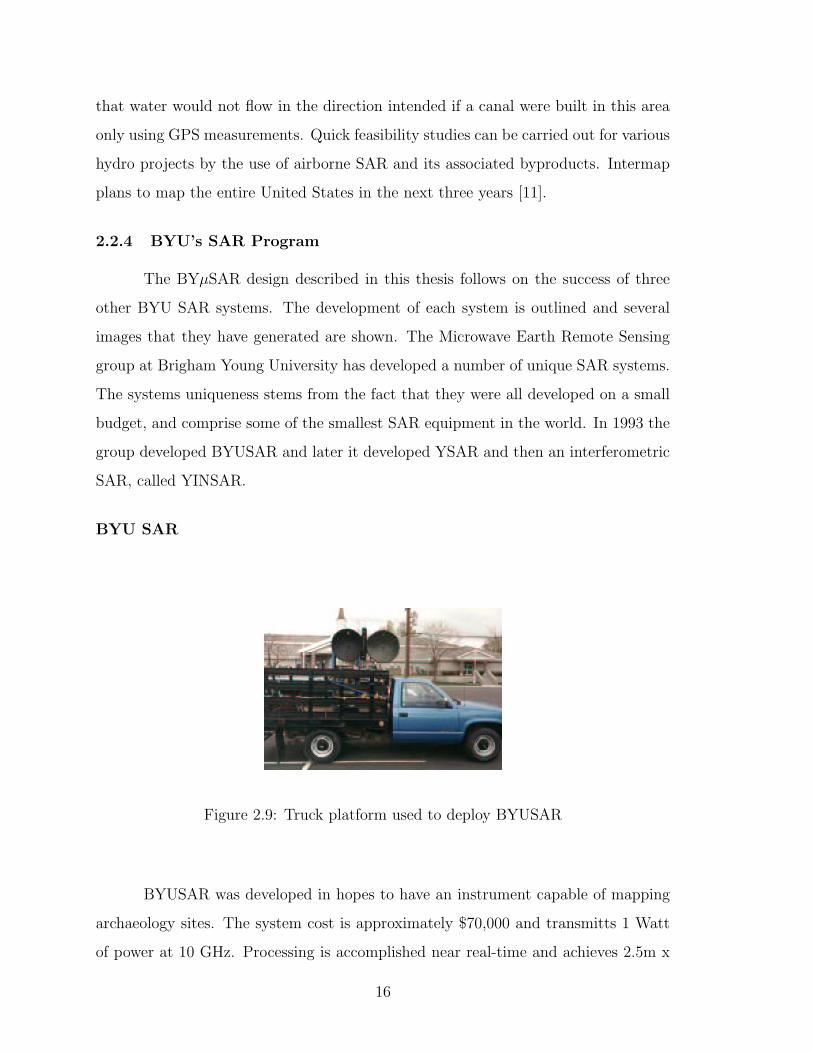
Figure 2.9: Truck platform used to deploy BYUSAR
BYUSAR was developed in hopes to have an instrument capable of mapping
archaeology sites. The system cost is approximately $70,000 and transmitts 1 Watt
of power at 10 GHz. Processing is accomplished near real-time and achieves 2.5m x
16
0.45m resolution. The system is small enough to be mounted aboard a small aircraft
and would be capable of imaging velocities of 168 m/s with near real-time processing
[12]. Due to budget and time constraints the system has only been deployed on a
truck platform shown in Figure 2.9.
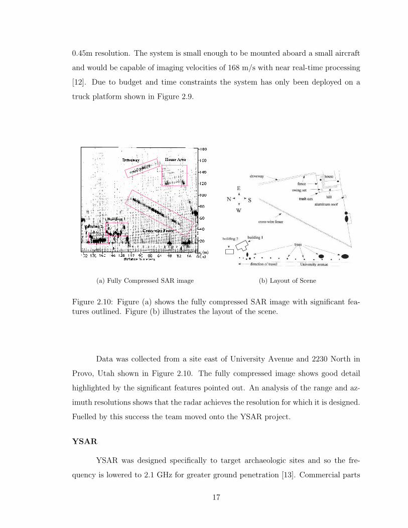
! "#
! "$
(a) Fully Compressed SAR image (b) Layout of Scene
Figure 2.10: Figure (a) shows the fully compressed SAR image with significant fea-tures outlined. Figure (b) illustrates the layout of the scene.
Data was collected from a site east of University Avenue and 2230 North in
Provo, Utah shown in Figure 2.10. The fully compressed image shows good detail
highlighted by the significant features pointed out. An analysis of the range and az-
imuth resolutions shows that the radar achieves the resolution for which it is designed.
Fuelled by this success the team moved onto the YSAR project.
YSAR
YSAR was designed specifically to target archaeologic sites and so the fre-
quency is lowered to 2.1 GHz for greater ground penetration [13]. Commercial parts
17
are used to design the majority of the system keeping the cost low. The platform for
this system is a Lance Piper with imaging altitudes of 305 to 610 m [14, 15]. The
overall system weighs 360 lbs with half of the weight in the battery pack.
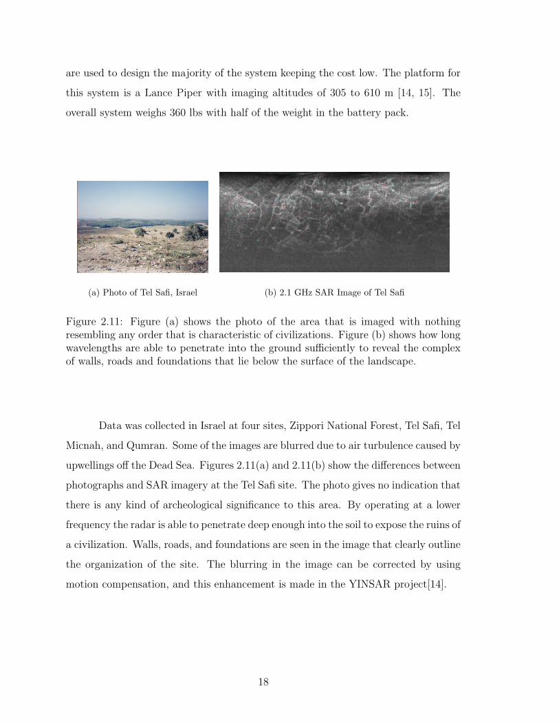
(a) Photo of Tel Safi, Israel (b) 2.1 GHz SAR Image of Tel Safi
Figure 2.11: Figure (a) shows the photo of the area that is imaged with nothingresembling any order that is characteristic of civilizations. Figure (b) shows how longwavelengths are able to penetrate into the ground sufficiently to reveal the complexof walls, roads and foundations that lie below the surface of the landscape.
Data was collected in Israel at four sites, Zippori National Forest, Tel Safi, Tel
Micnah, and Qumran. Some of the images are blurred due to air turbulence caused by
upwellings off the Dead Sea. Figures 2.11(a) and 2.11(b) show the differences between
photographs and SAR imagery at the Tel Safi site. The photo gives no indication that
there is any kind of archeological significance to this area. By operating at a lower
frequency the radar is able to penetrate deep enough into the soil to expose the ruins of
a civilization. Walls, roads, and foundations are seen in the image that clearly outline
the organization of the site. The blurring in the image can be corrected by using
motion compensation, and this enhancement is made in the YINSAR project[14].
18
(a) Cessna 337 N Skymaster (b) YINSAR Radar and Processing Boxes
Figure 2.12: Figure (a) shows the aircraft used to fly the YINSAR system. Figure(b) shows the YINSAR RF box and data acquisition system. The laptop is used tomonitor the location of the aircraft and control the radar.
YINSAR
BYU and Utah State University jointly own a Cessna 337 N Skymaster recon-
naissance plane seen in Figure 2.12(a). By using a push and pull propeller system
the plane is able to steer a straight course making it suitable for imaging [16]. The
Skymaster flies at an imaging altitude of 305 to 610 m and a nominal velocity of 60
m/s. YINSAR images a 600m swath at 2.16 km2/min with 1m by 0.5m resolution
[17]. The system operates at 9.9 GHz with a peak transmit power of 10W and a total
system power of 600 W. A differential GPS, kinematic GPS, and inertial measurement
unit are used to obtain the precise location and motion of the aircraft. The entire
system weighs 150 lbs and costs $200,000.
The processing is post-flight, which integrates data from the motion detectors
and the radar signals to generate well focused images with high resolution as seen
in Figure 2.13. This image includes the Marriot Center on BYU campus in the left
upper corner and the baseball stadium below it. Trees are apparent in this image
19
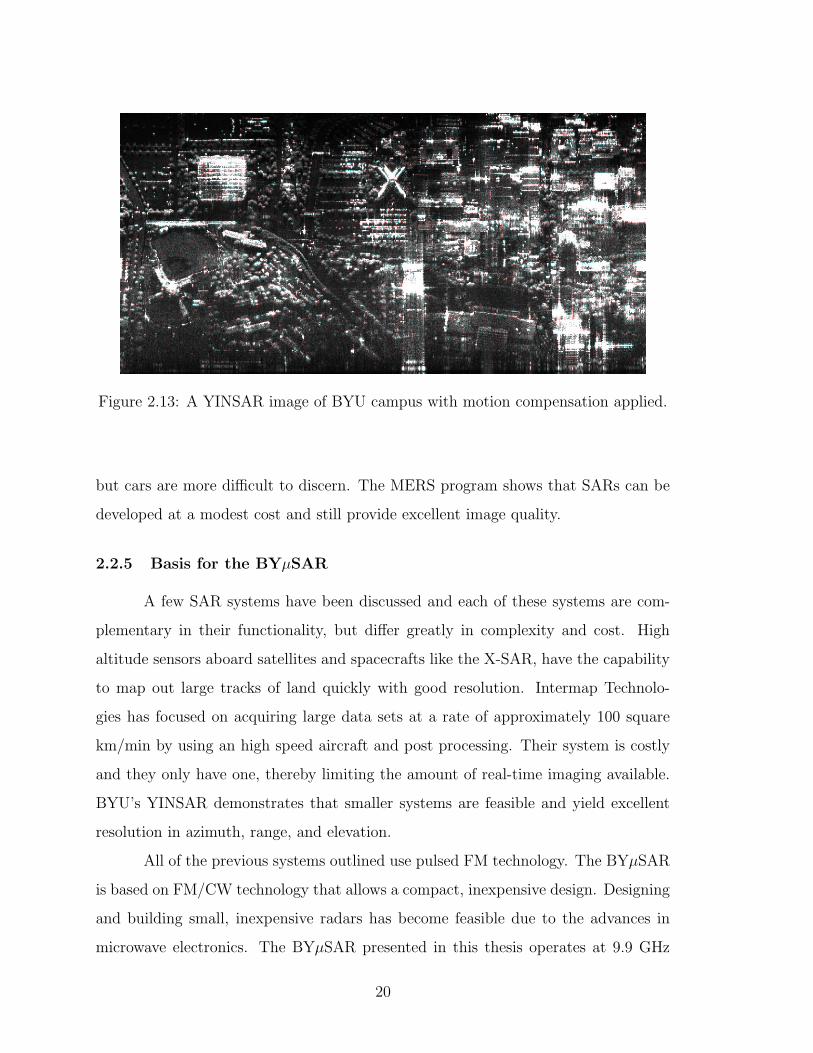
Figure 2.13: A YINSAR image of BYU campus with motion compensation applied.
but cars are more difficult to discern. The MERS program shows that SARs can be
developed at a modest cost and still provide excellent image quality.
2.2.5 Basis for the BYµSAR
A few SAR systems have been discussed and each of these systems are com-
plementary in their functionality, but differ greatly in complexity and cost. High
altitude sensors aboard satellites and spacecrafts like the X-SAR, have the capability
to map out large tracks of land quickly with good resolution. Intermap Technolo-
gies has focused on acquiring large data sets at a rate of approximately 100 square
km/min by using an high speed aircraft and post processing. Their system is costly
and they only have one, thereby limiting the amount of real-time imaging available.
BYU’s YINSAR demonstrates that smaller systems are feasible and yield excellent
resolution in azimuth, range, and elevation.
All of the previous systems outlined use pulsed FM technology. The BYµSAR
is based on FM/CW technology that allows a compact, inexpensive design. Designing
and building small, inexpensive radars has become feasible due to the advances in
microwave electronics. The BYµSAR presented in this thesis operates at 9.9 GHz
20
with a bandwidth of 200 MHz. Its resolution is 1.0x0.2m, platform velocity is 60
m/s, and has a variable swath width of 300 to 600 m. It can be used at an elevation
of 300 to 600 m and is capable of imaging 2.16 km2/min making the performance
the same as YINSAR. It only uses 1 mW of transmit power and consumes 12 W
of system power. It weighs 10 lbs including the waveguide antennas, cost $20,000
to develop, and the processing is accomplished post-flight using Matlab scripts. It
does not have motion compensation and data is collected using a digital sampling
oscilloscope, but these functions could be integrated into the design with minimal
impact to size, weight and cost.
Unmanned Aerial Vehicles (UAVs) are now developed to the point that they
are being used extensively by the military and commercial imaging companies. Small
aircraft are only able to carry a small payload and provide a conservative amount of
power. The technology used in BYµSAR is well suited for deployment on a UAV.
A SAR mounted on a UAV is well suited for a large number of applications such as
reconnaissance, terrain mapping, archeology, surveillance and surveying. Table 2.1
shows that the BYµSAR provides excellent resolution and has an advantage in size,
cost, and low power in comparison to the other systems already presented.
21
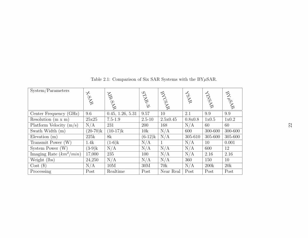
Table 2.1: Comparison of Six SAR Systems with the BYµSAR.
System/Parameters X-SAR
AIR
-SAR
STAR-3i
BYUSAR
YSAR
YIN
SAR
BYµSAR
Center Frequency (GHz) 9.6 0.45, 1.26, 5.31 9.57 10 2.1 9.9 9.9Resolution (m x m) 25x25 7.5-1.9 2.5-10 2.5x0.45 0.8x0.8 1x0.5 1x0.2Platform Velocity (m/s) N/A 231 200 168 N/A 60 60Swath Width (m) (20-70)k (10-17)k 10k N/A 600 300-600 300-600Elevation (m) 225k 8k (6-12)k N/A 305-610 305-600 305-600Transmit Power (W) 1.4k (1-6)k N/A 1 N/A 10 0.001System Power (W) (3-9)k N/A N/A N/A N/A 600 12Imaging Rate (km2/min) 17,000 235 100 N/A N/A 2.16 2.16Weight (lbs) 24,250 N/A N/A N/A 360 150 10Cost ($) N/A 10M 30M 70k N/A 200k 20kProcessing Post Realtime Post Near Real Post Post Post
22
Chapter 3
FM/CW SAR Techniques
FM/CW has not been generally accepted as a technology capable of gener-
ating quality SAR images for remote sensing, although others have published on its
uses for short range imaging [18, 19, 20, 21]. This chapter mathematically shows that
FM/CW based SAR does not introduce artifacts that deteriorate the quality of the
compressed image. This is done by first looking at the traditional use of FM/CW for
range detection and resolution. Then SAR geometry in airborne systems is explained
prior to an illustrative comparison of pulsed and CW SAR compression techniques.
Investigation into the quality of range and azimuth compression when using FM/CW
is made, and it is shown that FM/CW does not introduce significant phase errors.
A guide for designing a FM/CW system is given, outlining limitations and optimiza-
tions.
3.1 FM/CW Range Detection and Resolution
FM/CW is used in many systems that required range detection. The FM/CW
signal is first described and then the parameters used to determine performance are
identified. A simple example is shown illustrating the use of FM/CW to determine
the range to a target, and followed by a proof that the range resolution is determined
solely by the bandwidth of the FM/CW signal.
3.1.1 Range Detection
FM/CW is chosen because it is a convenient way to increase SNR, while re-
ducing the required system power level, complexity and cost. FM/CW is a continuous
23
wave (CW) radar that is frequency modulated (FM). This means that the source is
not turned off and on like a pulsed system, but it is continuously modulated. Typi-
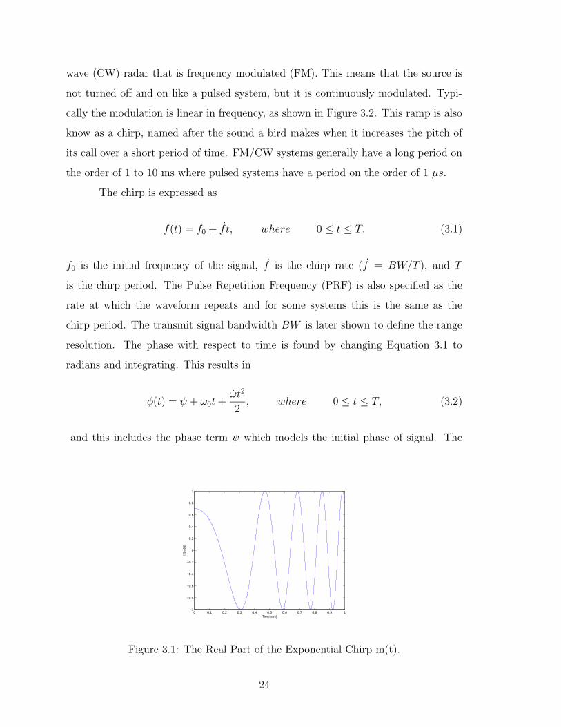
cally the modulation is linear in frequency, as shown in Figure 3.2. This ramp is also
know as a chirp, named after the sound a bird makes when it increases the pitch of
its call over a short period of time. FM/CW systems generally have a long period on
the order of 1 to 10 ms where pulsed systems have a period on the order of 1 µs.
The chirp is expressed as
f(t) = f0 + f t, where 0 ≤ t ≤ T. (3.1)
f0 is the initial frequency of the signal, f is the chirp rate (f = BW/T ), and T
is the chirp period. The Pulse Repetition Frequency (PRF) is also specified as the
rate at which the waveform repeats and for some systems this is the same as the
chirp period. The transmit signal bandwidth BW is later shown to define the range
resolution. The phase with respect to time is found by changing Equation 3.1 to
radians and integrating. This results in
φ(t) = ψ + ω0t+ωt2
2, where 0 ≤ t ≤ T, (3.2)
and this includes the phase term ψ which models the initial phase of signal. The
0 0.1 0.2 0.3 0.4 0.5 0.6 0.7 0.8 0.9 1−1
−0.8
−0.6
−0.4
−0.2
0
0.2
0.4
0.6
0.8
1
Time(sec)
ℜ[m
(t)]
Figure 3.1: The Real Part of the Exponential Chirp m(t).
24
phase expression is used in an exponential to represent the time domain waveform,
m(t) = eiφ(t), (3.3)
which is useful in radar analysis. Figure 3.1 is an illustrative plot of m(t) where
ω0 = 0, ω = 0.05 and ψ = π/4.
The usefulness of a FM/CW signal is shown by a simple example of a single
target. Figure 3.2 shows how a chirp may be used to measure the distance to an
object. A chirp begins at t = 0 sec and ends T sec later. The signal strikes a
single target at a distance x, and reflects back to the receiver in t0 seconds. The
frequency difference ∆f is measured by the vertical separation of the transmit and
receive signals. The distance x to the reflecting object is found using the similar
triangle theorem as related in the equation
x =toc
2,
∆f
to=BW
T, x =
c∆fT
2BW, (3.4)
where c is the speed of light.
3.1.2 Range Resolution and Processing Gain
Here it is shown that range resolution is controlled by only one system variable,
the transmit bandwidth BW . Processing gain is then demonstrated to be propor-
tional to the chirp period, making FM/CW very desirable.
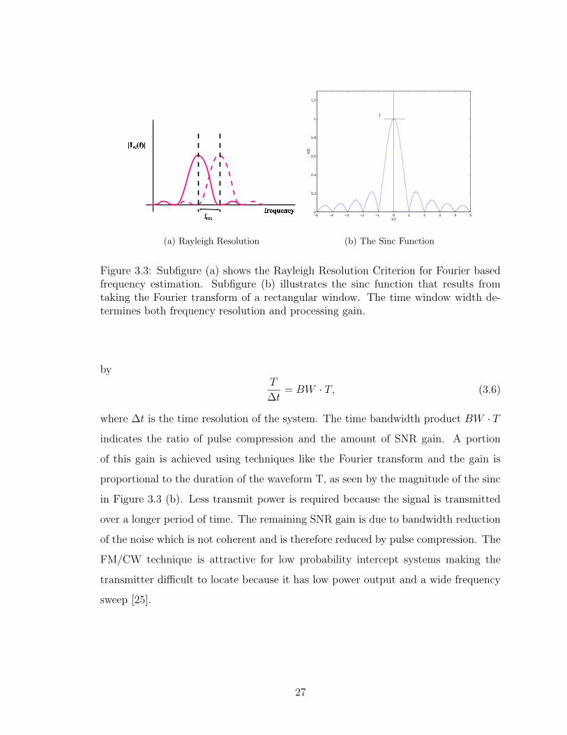
The range resolution of an arbitrary FM/CW system is based on the Rayleigh
resolution criterion. The criterion states that two components of equal intensity
should be considered to be just resolved when the first maximum from one component
sits at the first minimum from the other, as illustrated in Figure 3.3(a) [22]. The
distance between peaks is called the frequency resolution fres.
The resulting signal from a FM/CW system is the superposition of sinusoidal
signals. The Fourier transform a single sinusoid is a delta function. Consider two
independent frequencies that are windowed in time by a rectangular window with a
width equal to the chirp period T to determine the frequency resolution of a system.
25
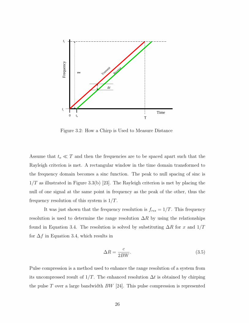
Time
Freq
uenc
y
Transm
it
Receiv
e
t 0 0 Τ
BW
f i
f f
∆ f
Figure 3.2: How a Chirp is Used to Measure Distance
Assume that to ¿ T and then the frequencies are to be spaced apart such that the
Rayleigh criterion is met. A rectangular window in the time domain transformed to
the frequency domain becomes a sinc function. The peak to null spacing of sinc is
1/T as illustrated in Figure 3.3(b) [23]. The Rayleigh criterion is met by placing the
null of one signal at the same point in frequency as the peak of the other, thus the
frequency resolution of this system is 1/T .
It was just shown that the frequency resolution is fres = 1/T . This frequency
resolution is used to determine the range resolution ∆R by using the relationships
found in Equation 3.4. The resolution is solved by substituting ∆R for x and 1/T
for ∆f in Equation 3.4, which results in
∆R =c
2BW. (3.5)
Pulse compression is a method used to enhance the range resolution of a system from
its uncompressed result of 1/T . The enhanced resolution ∆t is obtained by chirping
the pulse T over a large bandwidth BW [24]. This pulse compression is represented
26
(a) Rayleigh Resolution
−5 −4 −3 −2 −1 0 1 2 3 4 50
0.2
0.4
0.6
0.8
1
1.2
1/T
X(f
)
T
(b) The Sinc Function
Figure 3.3: Subfigure (a) shows the Rayleigh Resolution Criterion for Fourier basedfrequency estimation. Subfigure (b) illustrates the sinc function that results fromtaking the Fourier transform of a rectangular window. The time window width de-termines both frequency resolution and processing gain.
byT
∆t= BW · T, (3.6)
where ∆t is the time resolution of the system. The time bandwidth product BW · Tindicates the ratio of pulse compression and the amount of SNR gain. A portion
of this gain is achieved using techniques like the Fourier transform and the gain is
proportional to the duration of the waveform T, as seen by the magnitude of the sinc
in Figure 3.3 (b). Less transmit power is required because the signal is transmitted
over a longer period of time. The remaining SNR gain is due to bandwidth reduction
of the noise which is not coherent and is therefore reduced by pulse compression. The
FM/CW technique is attractive for low probability intercept systems making the
transmitter difficult to locate because it has low power output and a wide frequency
sweep [25].
27
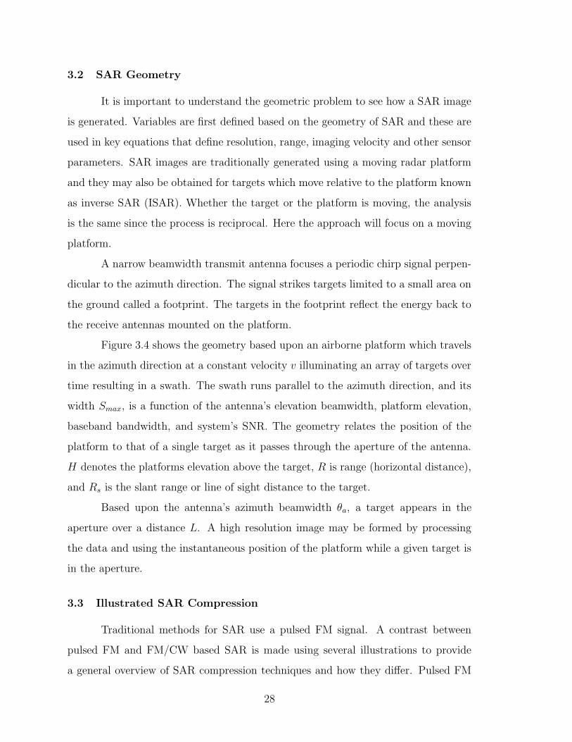
3.2 SAR Geometry
It is important to understand the geometric problem to see how a SAR image
is generated. Variables are first defined based on the geometry of SAR and these are
used in key equations that define resolution, range, imaging velocity and other sensor
parameters. SAR images are traditionally generated using a moving radar platform
and they may also be obtained for targets which move relative to the platform known
as inverse SAR (ISAR). Whether the target or the platform is moving, the analysis
is the same since the process is reciprocal. Here the approach will focus on a moving
platform.
A narrow beamwidth transmit antenna focuses a periodic chirp signal perpen-
dicular to the azimuth direction. The signal strikes targets limited to a small area on
the ground called a footprint. The targets in the footprint reflect the energy back to
the receive antennas mounted on the platform.
Figure 3.4 shows the geometry based upon an airborne platform which travels
in the azimuth direction at a constant velocity v illuminating an array of targets over
time resulting in a swath. The swath runs parallel to the azimuth direction, and its
width Smax, is a function of the antenna’s elevation beamwidth, platform elevation,
baseband bandwidth, and system’s SNR. The geometry relates the position of the
platform to that of a single target as it passes through the aperture of the antenna.
H denotes the platforms elevation above the target, R is range (horizontal distance),
and Rs is the slant range or line of sight distance to the target.
Based upon the antenna’s azimuth beamwidth θa, a target appears in the
aperture over a distance L. A high resolution image may be formed by processing
the data and using the instantaneous position of the platform while a given target is
in the aperture.
3.3 Illustrated SAR Compression
Traditional methods for SAR use a pulsed FM signal. A contrast between
pulsed FM and FM/CW based SAR is made using several illustrations to provide
a general overview of SAR compression techniques and how they differ. Pulsed FM
28
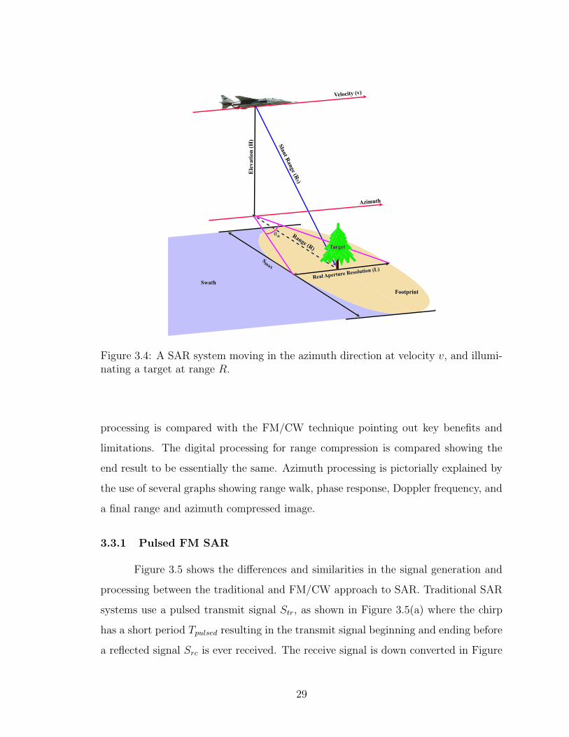
Figure 3.4: A SAR system moving in the azimuth direction at velocity v, and illumi-nating a target at range R.
processing is compared with the FM/CW technique pointing out key benefits and
limitations. The digital processing for range compression is compared showing the
end result to be essentially the same. Azimuth processing is pictorially explained by
the use of several graphs showing range walk, phase response, Doppler frequency, and
a final range and azimuth compressed image.
3.3.1 Pulsed FM SAR
Figure 3.5 shows the differences and similarities in the signal generation and
processing between the traditional and FM/CW approach to SAR. Traditional SAR
systems use a pulsed transmit signal Str, as shown in Figure 3.5(a) where the chirp
has a short period Tpulsed resulting in the transmit signal beginning and ending before
a reflected signal Src is ever received. The receive signal is down converted in Figure
29
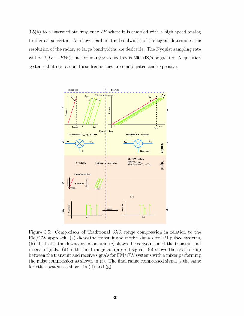
3.5(b) to a intermediate frequency IF where it is sampled with a high speed analog
to digital converter. As shown earlier, the bandwidth of the signal determines the
resolution of the radar, so large bandwidths are desirable. The Nyquist sampling rate
will be 2(IF +BW ), and for many systems this is 500 MS/s or greater. Acquisition
systems that operate at these frequencies are complicated and expensive.
Figure 3.5: Comparison of Traditional SAR range compression in relation to theFM/CW approach. (a) shows the transmit and receive signals for FM pulsed systems,(b) illustrates the downconversion, and (c) shows the convolution of the transmit andreceive signals. (d) is the final range compressed signal. (e) shows the relationshipbetween the transmit and receive signals for FM/CW systems with a mixer performingthe pulse compression as shown in (f). The final range compressed signal is the samefor ether system as shown in (d) and (g).
30
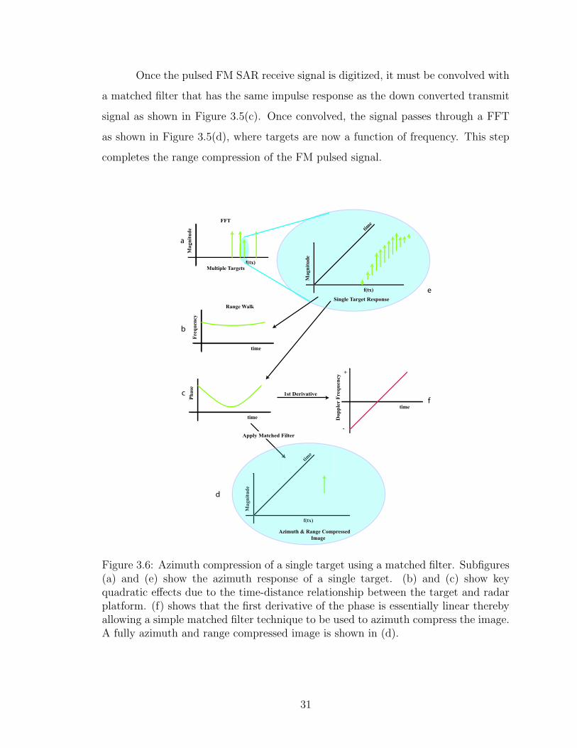
Once the pulsed FM SAR receive signal is digitized, it must be convolved with
a matched filter that has the same impulse response as the down converted transmit
signal as shown in Figure 3.5(c). Once convolved, the signal passes through a FFT
as shown in Figure 3.5(d), where targets are now a function of frequency. This step
completes the range compression of the FM pulsed signal.
Figure 3.6: Azimuth compression of a single target using a matched filter. Subfigures(a) and (e) show the azimuth response of a single target. (b) and (c) show keyquadratic effects due to the time-distance relationship between the target and radarplatform. (f) shows that the first derivative of the phase is essentially linear therebyallowing a simple matched filter technique to be used to azimuth compress the image.A fully azimuth and range compressed image is shown in (d).
31
3.3.2 FM/CW SAR
The FM/CW technique shown in Figure 3.5(e) shows how the chirp period
TFM is extended such that transmit and receive signals overlap. Transmit power
may be lowered due to the longer period that the signal is present contributing to
processing gain. The required overlap of the transmit and receive signals has a limiting
effect by making the SNR and range resolution dependant on range. The longer period
also restricts the velocity of the radar platform for proper azimuth sampling.
The delay time tx is the time it takes the transmit signal to travel to a target
x, reflect, and travel back to the receiver. The transmit and receive signals are mixed
using a microwave mixer to compress the signals to the baseband frequency in Figure
3.5(f). The baseband sample rate is dependent on range and is 2BWtx/TFM where
tx is the delay time for the farthest target of interest. For most systems tx << TFM
allowing the sample rates to be approximately 10 MS/s or less, and at these rates
standard video data acquisition circuits are sufficient. In Figure 3.5(g) the baseband
signal is passed through a FFT where the signal is fully range compressed. From this
point the SAR processing is the same and produces almost equivalent results.
The radar will image a single target multiple times in a single pass. Figure
3.6(a) shows a single target being selected, and then displays the FFT results over
time in Figure 3.6(e). The target appears small on the edge of the antenna beam,
it appears large in the middle of the beam and remains large until it reaches the
other edge of the beam where it drops off again. This is the azimuthal response
of a target and the azimuthal antenna pattern. Linear range walk and parabolic
phase response occur because the distance between the target and radar platform
changes parabolically. Range walk results when a single target moves across range
cells quadratically, as illustrated in Figure 3.6(b). This undesirable effect may be
removed by the use of algorithms in the signal processing [26].
The second result is a parabolic phase response, illustrated in Figure 3.6(c).
The frequency is found by taking the first derivative of the phase, which in this case
32
is the Doppler frequency. The Doppler frequency shown in Figure 3.6(f) is approx-
imately linear with time so it now looks like the chirps used in range compression.
An image is formed by applying the correct matched filter, and the image is then
range and azimuth compressed and is illustrated as a single point in azimuth time
and frequency in Figure 3.6(d). Mathematically it is later shown that both CW and
pulsed FM yield essentially the same results.
3.4 Range Compression Techniques
A detailed comparison between the FM/CW compression and the traditional
pulsed FM compression using the correlation function shows that differences occur
due to windowing effects. A comparison of ranges from 1 - 140 km is shown in Figure
3.9 indicating that FM/CW SAR has good range capabilities. This analysis assumes
that the radar platform is stationary relative to the target and thus eliminates the
complex azimuth effects that are addressed later.
3.4.1 FM/CW Range Compression
First, this derivation represents the time delay of a receive signal with a time
constant to which ignores azimuth effects but gives a simple result to model the range
compression. The final equation includes a convolution of the compressed signal with
a window that models the limits of integration.
A transmitted LFM signal is first considered in the exponential form,
mT (t) = ei(ψ+ω0t+ωt2
2) for 0 ≤ t ≤ T. (3.7)
Each received signal will have a time delay τ associated with the range of the reflecting
target and an amplitude A(τ) corresponding to the targets radar cross section. The
signal is a summation of all the targets in the aperture of the antenna yielding the
mathematical form
mR(t) =
∫ ∞
−∞
dτA(τ)mT (t− τ). (3.8)
33
Time
Freq
uenc
y
Transm
it
Receiv
e
t0 t1 t2 tn0Τ
BW
fi
ff
Figure 3.7: FM/CW Model of Transmitted and Return Signal Relationship.
Figure 3.7 shows the transmitted signal and the delayed copies that return
from respective ranges. Data acquisition time is limited between t0 to T because the
hardware implements range compression. This processing is accomplished by mixing
the transmitted and received signals followed by a lowpass filter. Mathematically
this is a multiplication of Equation 3.7 and the complex conjugate of Equation 3.8
resulting in the range compressed signal
iRC(t) = mT (t)m∗R(t), (3.9)
= ei(ψ+ω0t+ωt2
2)
∫ ∞
−∞
dτA∗(τ)e−i(ψ+ω0(t−τ)+ω(t−τ)2
2), (3.10)
=
∫ ∞
−∞
dτA∗(τ)ei(ω0τ+ωτt−ωτ2
2). (3.11)
34
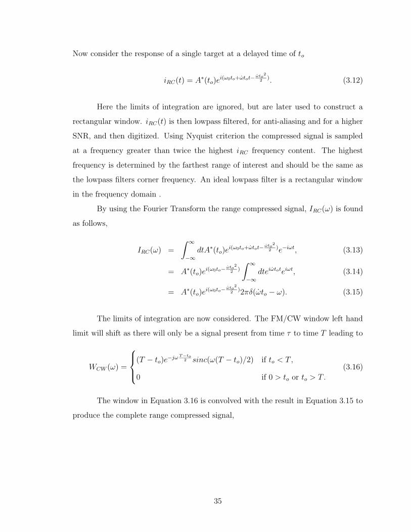
Now consider the response of a single target at a delayed time of to
iRC(t) = A∗(to)ei(ω0to+ωtot−
ωto2
2). (3.12)
Here the limits of integration are ignored, but are later used to construct a
rectangular window. iRC(t) is then lowpass filtered, for anti-aliasing and for a higher
SNR, and then digitized. Using Nyquist criterion the compressed signal is sampled
at a frequency greater than twice the highest iRC frequency content. The highest
frequency is determined by the farthest range of interest and should be the same as
the lowpass filters corner frequency. An ideal lowpass filter is a rectangular window
in the frequency domain .
By using the Fourier Transform the range compressed signal, IRC(ω) is found
as follows,
IRC(ω) =
∫ ∞
−∞
dtA∗(to)ei(ω0to+ωtot−
ωto2
2)e−iωt, (3.13)
= A∗(to)ei(ω0to−
ωto2
2)
∫ ∞
−∞
dteiωtoteiωt, (3.14)
= A∗(to)ei(ω0to−
ωto2
2)2πδ(ωto − ω). (3.15)
The limits of integration are now considered. The FM/CW window left hand
limit will shift as there will only be a signal present from time τ to time T leading to
WCW (ω) =
(T − to)e−jωT−to
2 sinc(ω(T − to)/2) if to < T,
0 if 0 > to or to > T.
(3.16)
The window in Equation 3.16 is convolved with the result in Equation 3.15 to
produce the complete range compressed signal,
35
ICW (ω) =
∫ ∞
−∞
dxIRC(ω − x)WCW (x) (3.17)
=
∫ ∞
−∞
dxA∗(to)ei(ω0to−
ωto2
2)2πδ(ωto − ω − x)
(T − to)e−jxT−to
2 sinc
(
xT − to
2
)
(3.18)
= 2π(T − to)A∗(to)ei(ωoto−
ωtoT2+
ω(T−to)2
)
sinc
(
(ωto − ω)T − to
2
)
. (3.19)
Several significant results are found in Equation 3.19. First the signal level is pro-
portional to the term (T − to) indicating that more energy is received with a larger
chirp period T , and that farther ranged targets have a diminished power level. The
argument of the sinc function (ωto−ω)T−to2 produces the second result. The ωto−ωterm shifts the center of the sinc function and the shift is dependant on the magni-
tude of ωto. TheT−to2
term determines the width of the sinc function and in turn the
resolution of the system. It is shown in section 3.1.2how this resolution translates to
the range resolution of the system. It is also seen that larger ranges will degrade the
range resolution as the sinc function broadens when T−to2
becomes smaller.
3.4.2 Pulsed FM Range Compression
FM Range compression is the traditional method for generating SAR images in
remote sensing applications. The following derivation parallels Robertson’s analysis
of the YINSAR autocorrelation range compression [3]. The development is reduced
to a single sideband chirp rather than a dual side band which Robertson developed
because a single sideband represents the type of modulation used in the BYµSAR.
A similar notation as Robertson’s is used so that the two derivations may be easily
compared, and then several substitutions allow the final result to be expressed in a
comparable form to Equation 3.19.
36
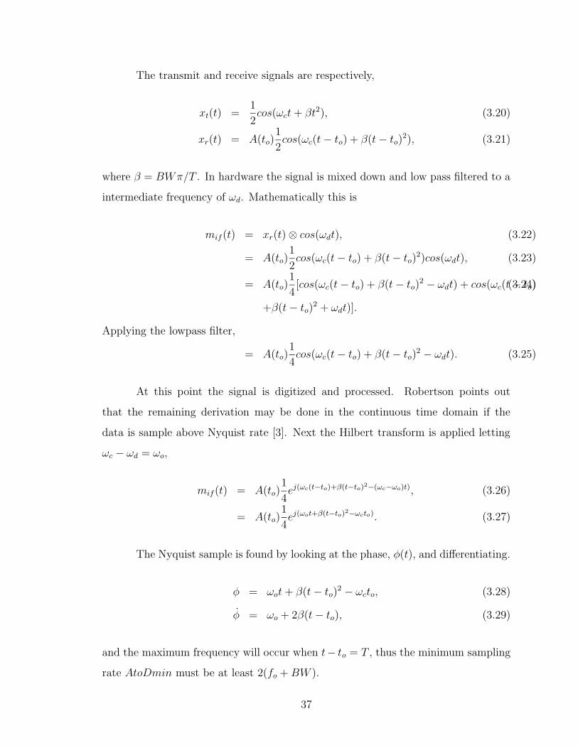
The transmit and receive signals are respectively,
xt(t) =1
2cos(ωct+ βt2), (3.20)
xr(t) = A(to)1
2cos(ωc(t− to) + β(t− to)2), (3.21)
where β = BWπ/T . In hardware the signal is mixed down and low pass filtered to a
intermediate frequency of ωd. Mathematically this is
mif (t) = xr(t)⊗ cos(ωdt), (3.22)
= A(to)1
2cos(ωc(t− to) + β(t− to)2)cos(ωdt), (3.23)
= A(to)1
4[cos(ωc(t− to) + β(t− to)2 − ωdt) + cos(ωc(t− to)(3.24)
+β(t− to)2 + ωdt)].
Applying the lowpass filter,
= A(to)1
4cos(ωc(t− to) + β(t− to)2 − ωdt). (3.25)
At this point the signal is digitized and processed. Robertson points out
that the remaining derivation may be done in the continuous time domain if the
data is sample above Nyquist rate [3]. Next the Hilbert transform is applied letting
ωc − ωd = ωo,
mif (t) = A(to)1
4ej(ωc(t−to)+β(t−to)
2−(ωc−ωo)t), (3.26)
= A(to)1
4ej(ωot+β(t−to)
2−ωcto). (3.27)
The Nyquist sample is found by looking at the phase, φ(t), and differentiating.
φ = ωot+ β(t− to)2 − ωcto, (3.28)
φ = ωo + 2β(t− to), (3.29)
and the maximum frequency will occur when t− to = T , thus the minimum sampling
rate AtoDmin must be at least 2(fo +BW ).
37
Assuming a infinite length matched filter of the form,
h(t) = ej(ωot+βt2), (3.30)
due to the large period T . The autocorrelation function is used to extract the range
compressed image m(t),
m(t) = mif (t)⊗ h∗(t), (3.31)
=
∫ ∞
−∞
mif (t+ τ)h∗(τ)dτ, (3.32)
= A(to)1
4
∫ ∞
−∞
ej(ωo(t+τ)+β(t−to+τ)2−ωcto)e−j(ωoτ+βτ
2)dτ, (3.33)
= A(to)1
4ej(ωot+β(−2tto+to
2+t2)−ωcto)
∫ ∞
−∞
ejβ(2tτ−2toτ)dτ, (3.34)
applying limits of integration,
= A(to)1
4ej(ωot+β(t−to)
2−ωcto)
∫ T−t+to
−t+to
ej2βτ(t−to)dτ, (3.35)
= A(to)1
4
ej(ωot+β(t−to)2−ωcto)
2jβ(t− to)(e2jβ(T−t+t0)(t−to) − e2jβ(−t+t0)(t−to)),(3.36)
= A(to)1
4
ejωot−jωcto
2jβ(t− to)(e2jβT (t−to)e−jβ(t−to) − e−jβ(t−to)), (3.37)
= A(to)1
4
ejωot−jωcto
β(t− to)ejβT (t−to)sin(βT (t− to))e−jβ(t−to), (3.38)
m(t) = A(to)T
4ejωo−jωctoejβ(t−to)(T−1)sinc(βT (t− to)). (3.39)
The last equation reveals the sinc effect due to the autocorrelation. The width
of the sinc is independent of the range dependant time t0, but is inversely proportional
to the bandwidth of chirp. The direct implication is that the range resolution is a
function of bandwidth and not the chirp period as shown in Section 3.1.2. The T/4
term at the beginning of the equation indicates the SNR of the signal is a direct
function of the chirp period, and increases with the period as was also shown.
Two differences in the range compression derivations must be pointed out in
order to contrast the two solutions. First, the pulsed solution has an intermediate
38

frequency ωd, which is zero in the FM/CW case. Second, the CW result is in the
frequency domain while the pulsed result is in the time domain.
By making the following subsitutions the CW and pulsed solutions converge
with slight, yet significant differences:
2β = ω, (3.40)
ωd = 0, (3.41)
(3.42)
The autocorrelation is carried out using
m(t) =
∫ ∞
−∞
m∗if (τ)h(t+ τ)dτ, (3.43)
and ignoring the limits of integration. Also applying the Fourier transform yields
exactly the same result for Equation 3.15 as found in the CW solution. This implies
that the difference in the two solutions lies in the window functions due to integration
limits. The window from the pulsed system has the limits τ = (−t + t0, T − t + t0)
that results in the window
Wac(ω) = Te−iω(t0+T2)sinc(ωT/2). (3.44)
The window is convolved with Equation 3.12:
IPulsed(ω) =
∫ ∞
−∞
dxIRC(ω − x)Wac(x) (3.45)
=
∫ ∞
−∞
dxA∗(to)ei(ω0to−
ωto2
2)2πδ(ωto − ω − x)
Te−ix(to+T2)sinc
(
xT
2
)
(3.46)
= 2πTA∗(to)ei(ωoto+ωto−
3ωt2o2
−ωtoT
2+ωT
2)
sinc
(
(ωto − ω)T
2
)
. (3.47)
39
3.4.3 Range Compression Contrast
The two range compressed solutions are contrasted by making them both a
function of range. Representing the frequency ω(Rs) = 2ωRs/c and the time delay
to the target to = 2Rs,o/c as a function of slant range allows the range compressed
signals to reduce to the forms
ICW (Rs) = 2π
(
T − 2Rs,o
c
)
A∗
(
2Rs,o
c
)
ei(
2ωoRs,oc
−ωRs,oT
c+ ωRs
c
(
T−2Rs,o
c
))
sinc
(
ω
c
(
T − 2Rs,o
c
)
(Rs,o −Rs)
)
, (3.48)
IPulsed(Rs) = 2πTA∗
(
2Rs,o
c
)
ei
(
2ωoRs,oc
+4ωRs,oRs
c2−
6ωR2s,o
c2−
ωRs,oT
c+ ωRsT
c
)
sinc
(
ωT
c(Rs,o −Rs)
)
. (3.49)
Equation 3.48 is compared to a computer simulated response for a target 7.3
m away in Figure 3.8. The effective width of the sinc waveform in both plots is 0.75m
comparing to the slant range resolution ∆Rs. The null to null width differs slightly
with the mathematical model measuring 2∆Rs and the simulation slightly less. The
plots for the pulsed FM model and associated simulation are almost identical to the
FM/CW model at 7.5m. As predicted earlier this changes with range as shown in
Figure 3.9.
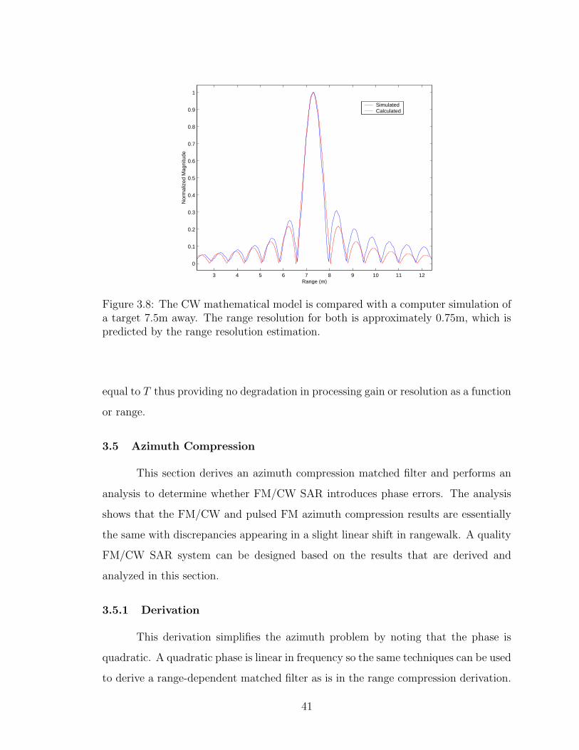
The plots in Figure 3.9 assume a FM/CW chirp period of 1 ms and a pulsed
period of 1 µs. The transmit power level of the pulsed system is raised to a sufficient
level to make the compressed signal level at 1 km the same. The effects of power
drop due to range in the radar equation are ignored. The range resolution and SNR
are both strongly effected when targets are approximately a hundredth (10µs) of the
chirp period (1ms) away, thereby limiting the effective range of the radar. The range
resolution effect is determined by the (T − 2Rs,o/c) term in the sinc function. The
processing gain drop is due to the multiplicative term (T − 2Rs,o/c) found at the
beginning of the window. When using auto correlation each of these terms are simply
40
3 4 5 6 7 8 9 10 11 12
0
0.1
0.2
0.3
0.4
0.5
0.6
0.7
0.8
0.9
1
Range (m)
Nor
mal
ized
Mag
nitu
de
Simulated Calculated
Figure 3.8: The CW mathematical model is compared with a computer simulation ofa target 7.5m away. The range resolution for both is approximately 0.75m, which ispredicted by the range resolution estimation.
equal to T thus providing no degradation in processing gain or resolution as a function
or range.
3.5 Azimuth Compression
This section derives an azimuth compression matched filter and performs an
analysis to determine whether FM/CW SAR introduces phase errors. The analysis
shows that the FM/CW and pulsed FM azimuth compression results are essentially
the same with discrepancies appearing in a slight linear shift in rangewalk. A quality
FM/CW SAR system can be designed based on the results that are derived and
analyzed in this section.
3.5.1 Derivation
This derivation simplifies the azimuth problem by noting that the phase is
quadratic. A quadratic phase is linear in frequency so the same techniques can be used
to derive a range-dependent matched filter as is in the range compression derivation.
41
0.995 0.996 0.997 0.998 0.999 1 1.001 1.002 1.003 1.004 1.0050
1
2
3
4
5
6
7x 10
−3
Range (km)
Mag
nitu
de
Direct Mix Autocorrelation
(a) Single Target at 1 kmwith a time delay to =6.67µsec
9.996 9.997 9.998 9.999 10 10.001 10.002 10.003 10.0040
1
2
3
4
5
6
x 10−3
Range (km)
Mag
nitu
de
Direct Mix Autocorrelation
(b) Single Target at 10 kmwith a time delay to =66.7µsec
69.996 69.997 69.998 69.999 70 70.001 70.002 70.003 70.0040
1
2
3
4
5
6
x 10−3
Range (km)
Mag
nitu
de
Direct Mix Autocorrelation
(c) Single Target at 70 kmwith a time delay to =0.48msec
139.995 139.996 139.997 139.998 139.999 140 140.001 140.002 140.003 140.004 140.0050
1
2
3
4
5
6
7x 10
−3
Range (km)
Mag
nitu
deDirect Mix Autocorrelation
(d) Single Target at 140 kmwith a time delay to =1msec
Figure 3.9: Mathematical model of single targets showing both SNR and resolutiondegradation. The transmit power level of the autocorrelated signal is 30 dB greaterthan the FM/CW level which shows the great power advantage of an FM/CW system.
A positive Doppler shift is added to the return signal as a SAR platform
approaches a target, decreases to zero shift at boarside, and then receives a negative
Doppler shift as the platform moves away from the target. The phase change φD of
the received signal is associated with the change in range δr from platform to target
42
due to the platform’s velocity as modelled by [26],
φD =4πfδr
c(3.50)
=4πδr
λ. (3.51)
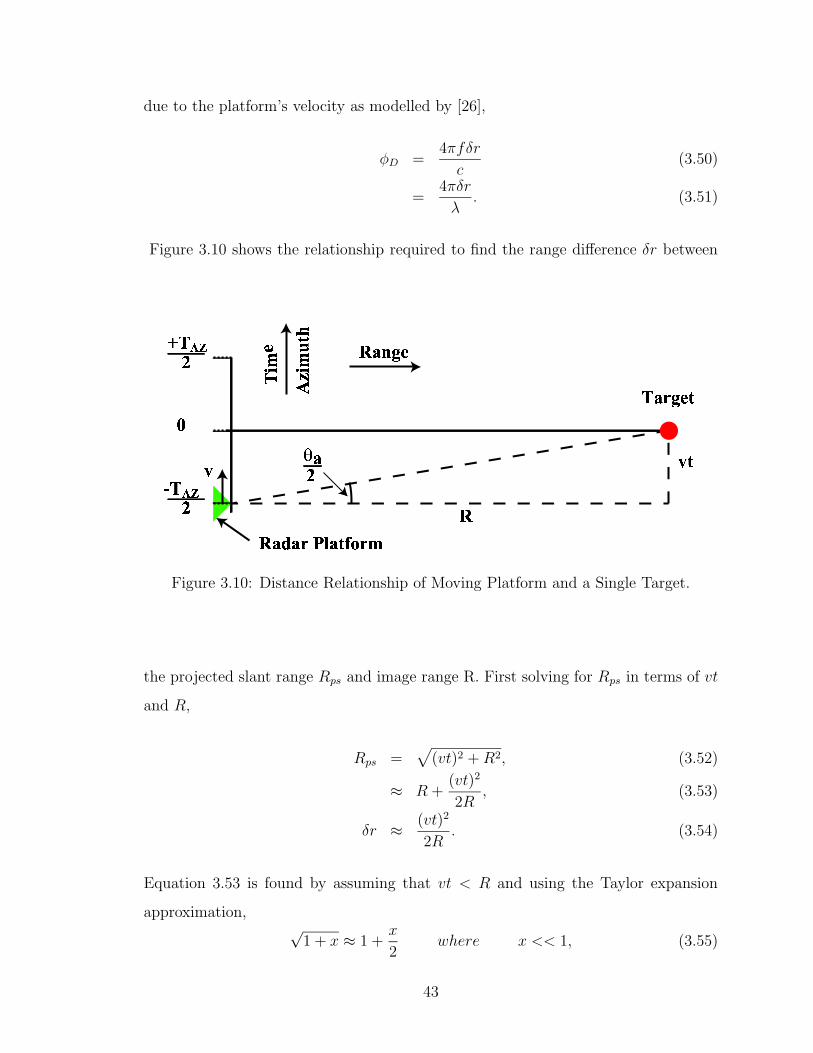
Figure 3.10 shows the relationship required to find the range difference δr between
!
" "
#$
% '&()
* '&()
+, )
Figure 3.10: Distance Relationship of Moving Platform and a Single Target.
the projected slant range Rps and image range R. First solving for Rps in terms of vt
and R,
Rps =√
(vt)2 +R2, (3.52)
≈ R +(vt)2
2R, (3.53)
δr ≈ (vt)2
2R. (3.54)
Equation 3.53 is found by assuming that vt < R and using the Taylor expansion
approximation,√1 + x ≈ 1 +
x
2where x << 1, (3.55)
43

and the error is x2/4. Substituting δr into Equation 3.51 yields
φD(t) =2πv2t2
λR. (3.56)
This time dependent phase may be considered an azimuth chirp by noticing
the phase is quadratic in time. Thus parameters such as bandwidth, chirp rate, and
period may be found to enable azimuth compression [27]. The azimuth frequency faz
is found by differentiating the phase
faz =2v2t
λR, (3.57)
and thus the azimuth chirp rate is found to be
faz =2v2
λR. (3.58)
The azimuth bandwidth BWAZ may be solved for by using the previously
defined chirp rate f = BW/T and extending this notion to the azimuth parameters.
First the azimuth period TAZ must be derived, and it is shown that the period is
dependent on the range of the target. From Figure 3.10 it is seen that
tan(θa/2) =vTaz2R
. (3.59)
Using the small angle approximation tan(θa/2) ≈ θa/2, the azimuth period can be
solved for, where
Taz =θaR
v. (3.60)
The azimuth bandwidth is defined by
BWaz = fazTaz, (3.61)
=2v2
λR
θaR
v, (3.62)
=2vθaλ
. (3.63)
44

The minimum pulse repetition frequency PRFmin must meet the Nyquist criterion
which is twice the azimuth bandwidth, namely
PRFmin =4vθaλ
. (3.64)
The derivation continues using the fact that the resolution is related to the velocity
of the platform and the signal bandwidth by
∆a =v
BWaz
, (3.65)
=λ
2θa, (3.66)
=d
2, (3.67)
where d is the physical dimension of the antenna in the azimuth direction. The last
equation also makes use of the antenna beamwidth approximation θa = λ/d. This
allows the azimuth LFM signal to be expressed as a function of the system parameters,
maz(t) = Arect
∣
∣
∣
∣
t
TAZ
∣
∣
∣
∣
ej2(2πfaz)t2 , (3.68)
= Arect
∣
∣
∣
∣
∣
tλR2∆av
∣
∣
∣
∣
∣
ej(2πv2
λR)t2 . (3.69)
A separate matched filter must be used for each range due to the filters dependence
on range. The azimuth matched filter haz(t) is simply the conjugate of the azimuth
signal such that
haz(t) = Arect
∣
∣
∣
∣
∣
tλR2∆av
∣
∣
∣
∣
∣
e−j(2πv2
λR)t2 (3.70)
3.5.2 FM/CW Phase Error Analysis
The following analysis proves that a properly designed FM/CW SAR system
will generate images that are properly compressed in both range and azimuth. The
range compression now accounts for the Doppler shift. Several approximations must
be used in order to simplify the complexity of the compression transforms. This results
45
in a solution that shows that there is minimal phase error introduced by FM/CW.
The analysis also shows that a linear rangewalk term dependent on the chirp period
T becomes more significant for longer periods. Equations are given to calculate the
amount of frequency shift expected for a set of system parameters and the amount of
phase error that is to be considered due to the approximations made.
The azimuth imaging is dependent upon the phase information obtained from
the range compression. SAR is restricted to having enough azimuth samples per
second in order to meet the Nyquist sampling criterion for azimuth compression.
SAR systems generally are designed with a short pulse of energy typically on the
order of 1µs in duration. With FM/CW the duration is lengthened in order to
achieve a direct mix between transmit and receive signals in hardware. As shown
earlier, the pulse must be sustained long enough to achieve adequate SNR and range
resolution, and in the BYµSAR the period is designed to be 1 ms. It is shown that
azimuth compression is not adversely affected by using FM/CW but a linear skew to
the range walk is enhanced.
Take Equation 3.11 and assume only one target. The equation will take the
form of
mrc(τ) = Aeωoτ+ωτt−ωτ2
2 . (3.71)
It is known that τ is quadratic in time and is related to projected slant range by
τ =2Rps
c, (3.72)
and using the approximation for range from Equation 3.53,
τ ≈ 2
c(R +
(vt)2
2R). (3.73)
Note that the distinction between time t in 3.71 and time t in 3.73. Time t represents
the time index into the chirp of the radar signal and resets to zero at the beginning
of every chirp. Time t, also known as ”slow time”, is the time index as the platform
46

approaches and passes the target and has the bounds of −Taz/2 to Taz/2. They are
related by
t = nT + t, (3.74)
where T is the chirp period and n is the index of the number of chirps. n is bounded
by −no and no, where
no =Taz2T
, (3.75)
=θaR
2vT. (3.76)
n is an integer, so no may be rounded to the nearest whole number. 2no also tells how
many azimuth samples are taken of a single target at a given range, and this value is
used to calculate the azimuth processing gain.
Next, an approximation reduces the order of t introduced by the t in τ . Squared
t results in
t2 = (nT )2 + 2nTt+ t2, (3.77)
which may be approximated as
t2 ≈ (nT )2 + 2nTt. (3.78)
The maximum amount of phase error caused by the approximation can be found
because t is bounded by T . The maximum error in τ is bounded, where
ετ <(vT )2
Rc, (3.79)
thus bounding the maximum error in the phase to
εph < ωoετ + ωT ετ −ωε2τ2, (3.80)
< ωo(vT )2
Rc+ ωT
(vT )2
Rc− ω(vT )4
2(Rc)2. (3.81)
The velocity is bounded by a maximum velocity vmax and can be found by solving
47

for v in Equation 3.63. The azimuth bandwidth is proportional to the inverse of the
period,
BWaz =1
2T, (3.82)
resulting in the expression
vmax =λ
4Tθa. (3.83)
The maximum velocity is substituted into Equation 3.81 with λ = c/fo,
εph <πc
8foθ2aR+πBWc
8f 2o θ2aR− πBWc3
256Tf 4o θ4aR
. (3.84)
This equation is true for any system in general, and it can be seen that the minimum
range of interest needs to be specified to obtain the correct result. The phase error is
0.039 radians at a 10 m range using BYµSAR airborne parameters. This error may
be reduced by a factor of 8 by using the approximation,
t2 ≈ (nT )2 + (2n+ 1)Tt− T 2
8, (3.85)
but for simplicity the approximation in Equation 3.78 is used.
τ is now approximated as
τ ≈ 2R
c+
v2
RC((nT )2 + 2nTt), (3.86)
but can be more easily handled with the substitution τ = a+ bt, where
a =2R
c+
(vnT )2
Rcand (3.87)
b =v2
Rc(2nT ). (3.88)
Equation 3.71 in now expressed as
mrc(t) ≈ Aei(ωoa−ωa2
2+[ωob+ωa−ωab]t+[ωb−
ωb2
2]t2). (3.89)
48
A Fourier transform can be used by making another approximation to get an analytic
solution. This time the t2 term is dropped. By using the fact that t is bounded by
T, it is shown that the phase error introduced by the drop is
εph2 = ωb
(
1− b
2
)
T 2, (3.90)
= ω2v2nT 3
RC
(
1− v2nT
RC
)
, (3.91)
=ωvθaT
2
c
(
1− vθa2c
)
, (3.92)
=πBW
fo
(
1− 1
8foT
)
. (3.93)
Equation 3.92 substitutes no for its maximum value derived in Equation 3.76, and
Equation 3.93 substitutes in the maximum velocity and simplifies. The result is
general for any system and is based solely on system parameters. A maximum error
of 0.065 radians results from the BYµSAR parameters.
The final time waveform is solved by dropping the t2 in Equation 3.89, where
mrc(t) ≈ Aei(ωoa−ωa2
2+[ωob+ωa−ωab]t). (3.94)
The signal essentially exists from time a to T . Thus the transform becomes
Mrc(ω) =
∫ T
a
mrc(t)e−iωtdt, (3.95)
= Aei(ωoa−ωa2
2)
∫ T
a
ei([ωob+ωa−ωab]t)e−iωtdt, (3.96)
= Aei(ωoa−ωa2
2)
∫ T
a
ei(ωob+ωa−ωab−ω)tdt, (3.97)
Mrc(ω, n) = Aei(ωoa−ωa2
2+(ωob+ωa−ωab−ω)
T+a2)(T − a)
∗sinc(
(ωob+ ωa− ωab− ω)T − a2
)
. (3.98)
The parameter n is added to the last equation to indicate the dependence of a and
b on n. A two dimensional equation results that represents the response of a single
49
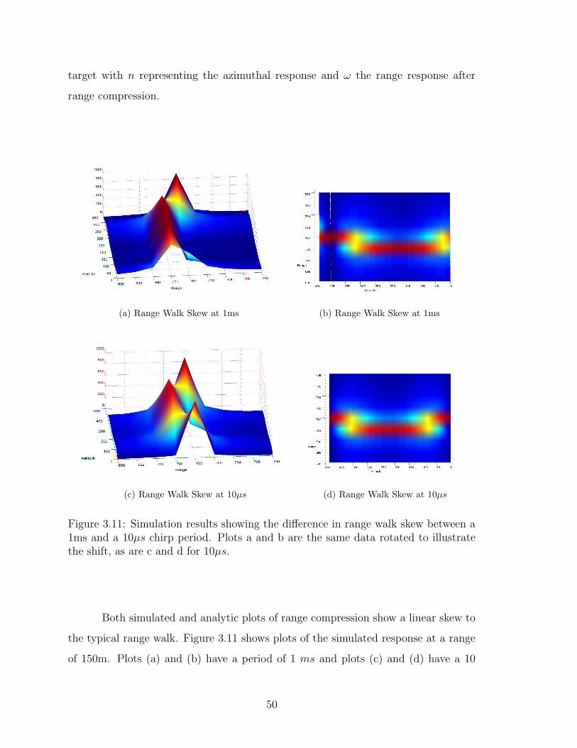
target with n representing the azimuthal response and ω the range response after
range compression.
(a) Range Walk Skew at 1ms (b) Range Walk Skew at 1ms
(c) Range Walk Skew at 10µs (d) Range Walk Skew at 10µs
Figure 3.11: Simulation results showing the difference in range walk skew between a1ms and a 10µs chirp period. Plots a and b are the same data rotated to illustratethe shift, as are c and d for 10µs.
Both simulated and analytic plots of range compression show a linear skew to
the typical range walk. Figure 3.11 shows plots of the simulated response at a range
of 150m. Plots (a) and (b) have a period of 1 ms and plots (c) and (d) have a 10
50

µs period. The term ωob(T + a)/2 in the exponent of Equation 3.98 is found to be
the contributor to this effect. The shift in frequency is found by substituting in the
a and b variables,
ωlrw =2ωov
2nT (T + 2Rc+ (vnT )2
Rc)
2Rc. (3.99)
A dominantly linear range walk term in frequency becomes apparent because n is
linear.
A single target fixed in range has all constants with the exception of n which
ranges from −no to no. Substituting 2no in place of n sets the maximum bound for
the amount of frequency shift expected from −Taz to Taz,
ωshift =ωovθa(T + 2R
c+ (vnT )2
Rc)
c. (3.100)
The result is dependent on range, and this is true for only FM/CW SAR systems.
The response for a pulsed FM SAR is
ωshift =ωovθaT
c. (3.101)
The period T determines that amount of skew in the range walk, and for pulsed
systems T is so small that the effect is negligible. For FM/CW systems this must be
considered as well as the range dependence, and appropriate algorithms may be used
to compensate for the skew.
The phase integrity of a FM/CW SAR is the main question that this thesis is
to address. The first two terms ωoa − ωa2
2dominate the phase response in Equation
3.98 and determine the phase of the signal for every value of n. Substituting back in
the variable a results in
φdop =2ωoR
c+ωov
2n2T 2
Rc+
2ωR2
c2+
2ωv2n2T 2
c2+ωv4n4T 4
2c2R4. (3.102)
The only variable with time is n so any term that does not have dependence on n
may be dropped. Two n2 terms are left and a n4 term. Next the maximum amount
51
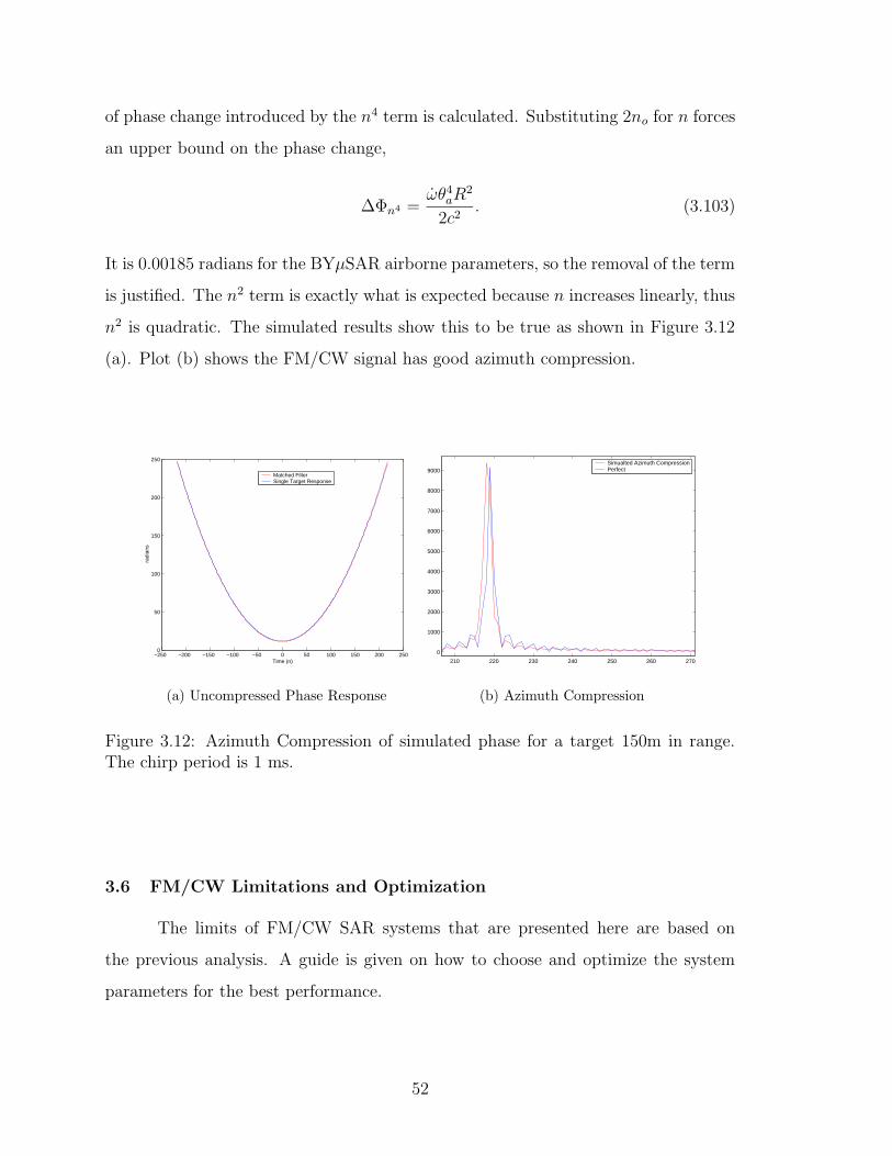
of phase change introduced by the n4 term is calculated. Substituting 2no for n forces
an upper bound on the phase change,
∆Φn4 =ωθ4aR
2
2c2. (3.103)
It is 0.00185 radians for the BYµSAR airborne parameters, so the removal of the term
is justified. The n2 term is exactly what is expected because n increases linearly, thus
n2 is quadratic. The simulated results show this to be true as shown in Figure 3.12
(a). Plot (b) shows the FM/CW signal has good azimuth compression.
−250 −200 −150 −100 −50 0 50 100 150 200 2500
50
100
150
200
250
Time (n)
rad
ians
Matched FilterSingle Target Response
(a) Uncompressed Phase Response
210 220 230 240 250 260 270
0
1000
2000
3000
4000
5000
6000
7000
8000
9000Simualted Azimuth CompressionPerfect
(b) Azimuth Compression
Figure 3.12: Azimuth Compression of simulated phase for a target 150m in range.The chirp period is 1 ms.
3.6 FM/CW Limitations and Optimization
The limits of FM/CW SAR systems that are presented here are based on
the previous analysis. A guide is given on how to choose and optimize the system
parameters for the best performance.
52
Three key limitations on the chirp period are found when implementing FM/CW
based SAR. First the range is limited by the degree to which the range resolution is
able to degrade. From Equation 3.48 it is seen that the range resolution is degraded
by the T-2Rs/c term located in the sinc function. If the term drops to T/2 then
the resolution doubles, and if to T/4 it quadruples and so on. Equation 3.5 may be
modified to account for this effect by letting
∆Rs,mod =c
2BW
(
cT
cT − 2Rs
)
. (3.104)
Second, platform velocity limits the chirp period. The maximum velocity is related
to the period by Equation 3.83 for a system where PRFmin = 1/T , and it is seen
that the relationship is inversely proportional. Knowing the type of platform to be
used, realistic speeds for imaging may be calculated and used to determine a upper
bound of the period. The PRFmin and 1/T may be equal depending on the type
of modulation being used. In general, PRFmin must be less than or equal to 1/T
in order to ensure that proper azimuth sampling is occurring. This puts an upper
limit on the range of T . The PRFmin is related to the velocity by Equation 3.64
and so it is seen that there are fundamental relationships between the PRF, v and
T. Therefore FM/CW based SAR is best suited for shorter ranged remote sensing of
approximately a 10 km maximum range. The platform is also velocity limited and
would not be appropriate in high speed aircraft.
Finally, the period is limited by the amount of range walk skew that is permis-
sible. No attempt is made to perform any range walk compensation which is generally
used in high performance systems. These algorithms can be modified to encompass
the linear skew.
It has been shown that FM/CW has a number of benefits that are maximized
when the period is maximized. Long pulse periods are achievable because the transmit
and receive signals are required to simultaneously exist. High SNR and low transmit
power are a result of the long pulse period. A low baseband frequency, simpler
electronics, feed-through rejection, and less digital processing power are results of
53

directly mixing the transmit and receive signals to dechirp or compress the receive
signal.
A guideline for maximizing the period of a FM/CW SAR system is outlined
below:
1. Choose a frequency for the desired electromagnetic interaction with the scene
and within licensing limitations.
2. Set the bandwidth to achieve the desired range resolution allowing for any
increase due to large periods. This may also be limited by licensing limitations.
3. Determine the desired azimuth resolution and set the antenna azimuthal beamwidth
according to Equation 3.66.
4. Determine the maximum and minimum ranges of interest.
5. Determine the maximum velocity that the platform will achieve during imaging.
This sets the minimum PRF.
6. Determine the chirp type whether sawtooth or triangular. Also determine
whether both the up and down chirps or only one will be used. Note that
all previous derivations assumed a sawtooth type chirp with a 100% duty cycle.
7. Maximize T and ensure that the following satisfy the desired performance cri-
terion:
Range walk ⇒ ωshift = ωovθa(T + 2Rc+ (vnT )2
Rc)/c
Phase error ⇒ ∆Φn4 = ωθ4aR2
2c2
PRFmin < 1/T
Make sure the approximations in Equations 3.84 and 3.93 are within the
specified tolerance.
54

Chapter 4
BYµSAR System Design
A prototype system is required to verify that FM/CW can be used to generate
quality SAR images. This chapter defines the specifications for an airborne and track
system, and builds a design around them. The first section gives a system block
diagram and a list of modules that make up the complete SAR. The next two sections
divide these modules into two groups, transmitter and receiver. The whole assembly
of the system is reviewed, and then the system’s SNR is calculated based on the radar
equation and noise analysis.
4.1 BYµSAR Specifications
Airborne and track specifications are listed in this section with attention paid
to slant range calculations and the dependence of range resolution on the elevation of
the platform. The system block diagram is given followed by a list identifying each
module and its interconnects.
4.1.1 Airborne System Specifications
This SAR system is designed so that it can be used in the same aircraft as
YINSAR. The same geometrical parameters and velocity for the aircraft are also
used. The geometry, as illustrated in Figure 4.1, helps define the maximum and
minimum slant range from a chosen elevation and swath width. The aircraft flies at
an elevation between 300m and 600m. The look angles are φ1 = 45 and φ2 = 65.
Rmin = 300m, Rmax = 600m, Rs,min = 424m, and Rs,max = 671m for the 300m
55
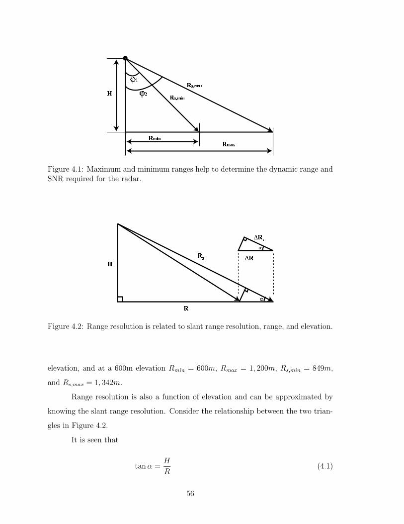
Figure 4.1: Maximum and minimum ranges help to determine the dynamic range andSNR required for the radar.
Figure 4.2: Range resolution is related to slant range resolution, range, and elevation.
elevation, and at a 600m elevation Rmin = 600m, Rmax = 1, 200m, Rs,min = 849m,
and Rs,max = 1, 342m.
Range resolution is also a function of elevation and can be approximated by
knowing the slant range resolution. Consider the relationship between the two trian-
gles in Figure 4.2.
It is seen that
tanα =H
R(4.1)
56
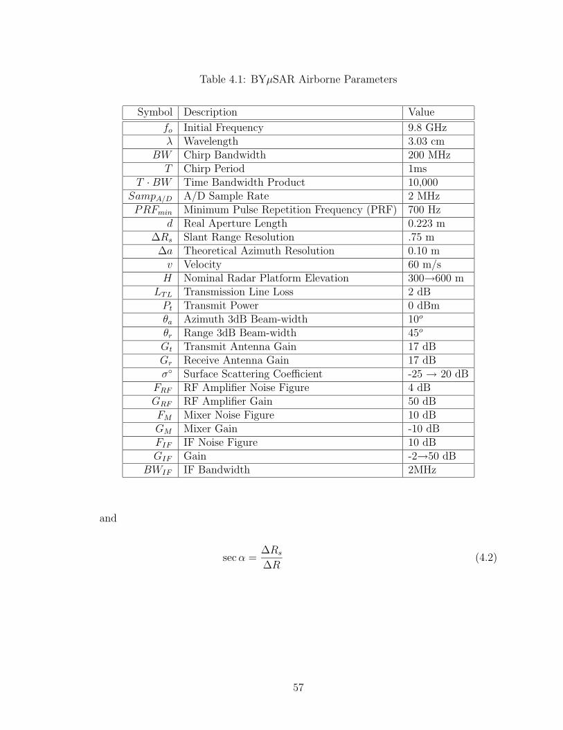
Table 4.1: BYµSAR Airborne Parameters
Symbol Description Value
fo Initial Frequency 9.8 GHzλ Wavelength 3.03 cm
BW Chirp Bandwidth 200 MHzT Chirp Period 1ms
T ·BW Time Bandwidth Product 10,000SampA/D A/D Sample Rate 2 MHzPRFmin Minimum Pulse Repetition Frequency (PRF) 700 Hz
d Real Aperture Length 0.223 m∆Rs Slant Range Resolution .75 m∆a Theoretical Azimuth Resolution 0.10 mv Velocity 60 m/sH Nominal Radar Platform Elevation 300→600 m
LTL Transmission Line Loss 2 dBPt Transmit Power 0 dBmθa Azimuth 3dB Beam-width 10o
θr Range 3dB Beam-width 45o
Gt Transmit Antenna Gain 17 dBGr Receive Antenna Gain 17 dBσ Surface Scattering Coefficient -25 → 20 dB
FRF RF Amplifier Noise Figure 4 dBGRF RF Amplifier Gain 50 dBFM Mixer Noise Figure 10 dBGM Mixer Gain -10 dBFIF IF Noise Figure 10 dBGIF Gain -2→50 dB
BWIF IF Bandwidth 2MHz
and
secα =∆Rs
∆R(4.2)
57
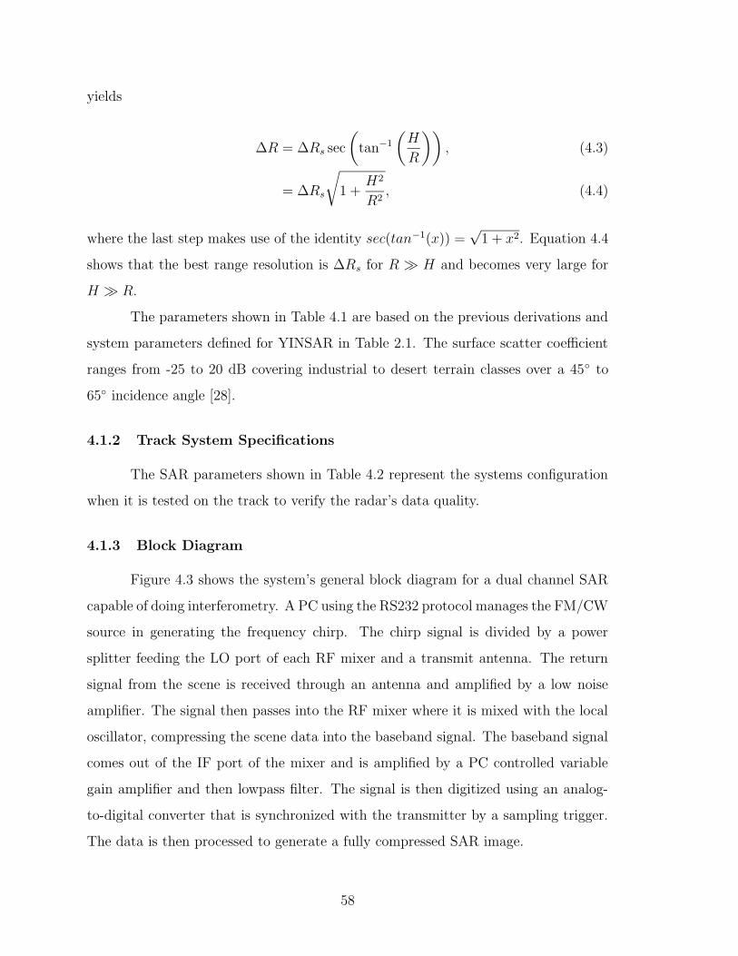
yields
∆R = ∆Rs sec
(
tan−1(
H
R
))
, (4.3)
= ∆Rs
√
1 +H2
R2, (4.4)
where the last step makes use of the identity sec(tan−1(x)) =√1 + x2. Equation 4.4
shows that the best range resolution is ∆Rs for R À H and becomes very large for
H À R.
The parameters shown in Table 4.1 are based on the previous derivations and
system parameters defined for YINSAR in Table 2.1. The surface scatter coefficient
ranges from -25 to 20 dB covering industrial to desert terrain classes over a 45 to
65 incidence angle [28].
4.1.2 Track System Specifications
The SAR parameters shown in Table 4.2 represent the systems configuration
when it is tested on the track to verify the radar’s data quality.
4.1.3 Block Diagram
Figure 4.3 shows the system’s general block diagram for a dual channel SAR
capable of doing interferometry. A PC using the RS232 protocol manages the FM/CW
source in generating the frequency chirp. The chirp signal is divided by a power
splitter feeding the LO port of each RF mixer and a transmit antenna. The return
signal from the scene is received through an antenna and amplified by a low noise
amplifier. The signal then passes into the RF mixer where it is mixed with the local
oscillator, compressing the scene data into the baseband signal. The baseband signal
comes out of the IF port of the mixer and is amplified by a PC controlled variable
gain amplifier and then lowpass filter. The signal is then digitized using an analog-
to-digital converter that is synchronized with the transmitter by a sampling trigger.
The data is then processed to generate a fully compressed SAR image.
58

Table 4.2: BYµSAR Track Parameters
Symbol Description Value
fo Initial Frequency 9.8 GHzλ Wavelength 3.03 cm
BW Chirp Bandwidth 200 MHzT Chirp Period 500 µs
T ·BW Time Bandwidth Product 1000SampA/D A/D Sample Rate 100 kHzPRFmin Minimum Pulse Repetition Frequency (PRF) 2.93 Hz
θa Azimuth 3dB Beam-width 10o
θr Range 3dB Beam-width 45o
d Real Aperture Length 0.223 m∆Rs Slant Range Resolution 0.75 m∆a Theoretical Azimuth Resolution 0.10 mV Velocity 0.327 m/sH Nominal Radar Platform Elevation 0 m
The system design is divided into modules by functionality. Each module is
designed for a general interface such that blocks may be changed to accommodate
changes in system requirements.
1. RF Transmitter - contains only the high frequency components of the FM/CW
source and is encased in a machined aluminum case. The module connects
to the driver plane by a series of feed-troughs and a MCX RF connector. It
connects to the transmit antenna and RF mixers through SMA semirigid coax
cables.
2. Driver/Power Plane - this module contains the digital logic for the FM/CW
source which includes a PECL frequency counter and a CMOS waveform gen-
erator. A RS232 connection allows a PC to communicate with the waveform
generator. The plane routes signals between the other modules and distributes
power to them. Voltage regulation for each LNA block is also provided on the
plane.
59
! #"$ %$&'(')$
* " + ' , - +. ++"
/ 0 - +. ++"
1" ')!2 "$+3- ,45 6
7 8:9; ')- <45 =6
%>&8? 45
7 8@% " ')'A 5 * "$+ ' , '(' +
7B=+
"C ,45 +D* C
/E F
GIHJK
L)H
/ 0 - +. ++"
/E F
GIHJK
L)H
7 8:9; ')- <45 =6
7 8@% " ')'A 5
* "$+ ' , '(' +7B=+
1" ')!2 "$+3- ,45 6
MNON#PAQSRUT&P>V WX YZ Y
WX YZ Y
Figure 4.3: Simplified Block Diagram of SAR System.
3. LNA - two 50 dB low noise amplifiers with a 4 dB noise figure. Each LNA is
encased in a machined aluminum case with SMA connectors to interface with
the antennas and RF mixers.
4. RF Mixer - the mixer is encased in a machined aluminum case with SMA
connectors to interface with the LNA, RF transmitter, and baseband module.
5. Baseband Module- this module includes a variable gain amplifier with filtering
for baseband processing. It receives signals from the RF mixers via the SMA
semirigid coaxial cables. The gain is controlled by a PC that communicates
60
via a RS232 protocol. It sends the amplified signal to the digitizer through a
BNC connector and connects to the driver/power plane through a card edge
connector.
6. Power Module - Input power is ±12 Volts, which is divided into a variety of
voltages and power planes. The module plugs into a card edge connector in
the driver/power plane where the power is distributed to components and other
modules.
7. Digitizer and Image Processor - the digitizer is a oscilloscope with deep memory
acquisition. The image processing is accomplished using Matlab.
4.2 Transmitter
A unique way to linearize the chirp from a VCO is shown where a microcon-
troller sets the VCO’s tuning voltage and then measures its response. The transmitter
is discussed in two parts, the RF module and the driver. The RF module contains
parts that radiate high frequency emissions and should be isolated from noise sources.
The driver is separated into two sections based on functionality, which are the wave-
form generator and phase counter circuit. The waveform circuit takes the digital
values calculated from the microcontroller and turns them into a clean analog signal,
where the phase counter measures the frequency output of the VCO. The algorithms
that control these operations are explained in the algorithms section.
4.2.1 LFM Generation
Frequency sweep nonlinearity is considered a limiting factor in FM/CW range
resolution and a contributor to spectral clutter in the range compressed signal [29, 30].
Many different methods have been used to achieve high linearity in the FM signal with
varying degrees of success [31, 32, 33]. A unique and successful method to linearize
the output of a VCO is introduced.
The difficulty in producing a linear chirp comes from the fact that VCOs do not
exhibit a linear tuning voltage as exaggerated in Figure 4.4 (a). The tuning voltage
61
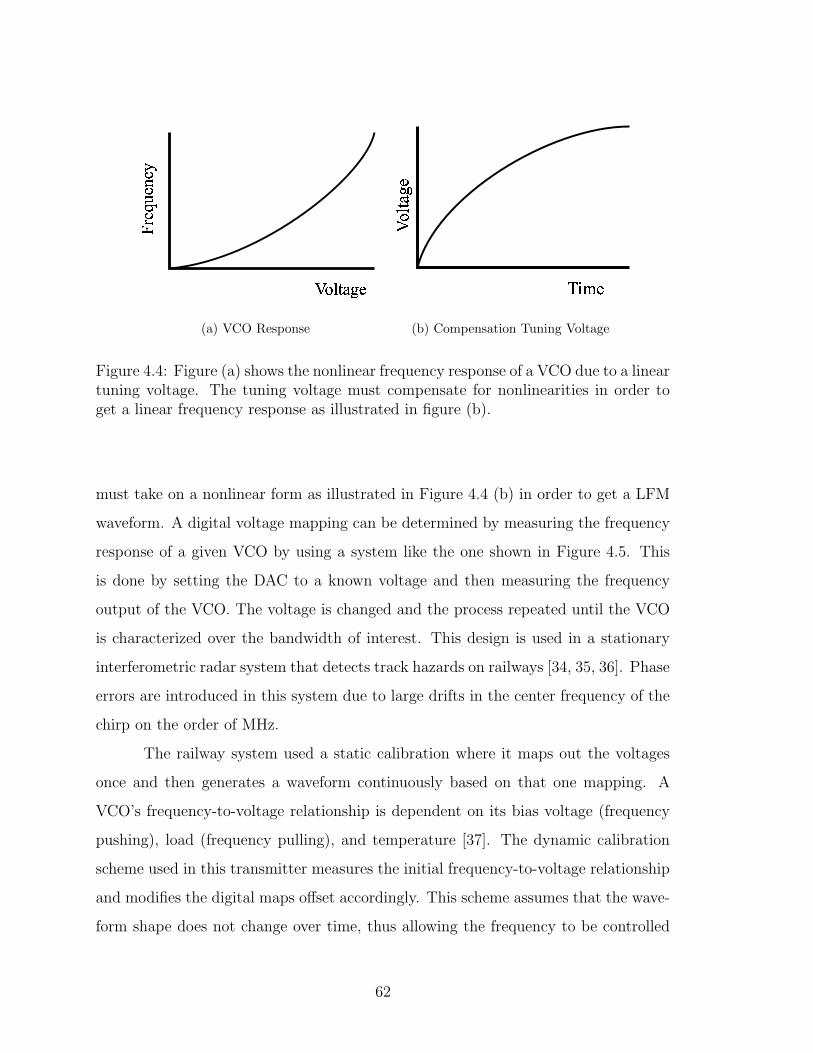
(a) VCO Response
!
(b) Compensation Tuning Voltage
Figure 4.4: Figure (a) shows the nonlinear frequency response of a VCO due to a lineartuning voltage. The tuning voltage must compensate for nonlinearities in order toget a linear frequency response as illustrated in figure (b).
must take on a nonlinear form as illustrated in Figure 4.4 (b) in order to get a LFM
waveform. A digital voltage mapping can be determined by measuring the frequency
response of a given VCO by using a system like the one shown in Figure 4.5. This
is done by setting the DAC to a known voltage and then measuring the frequency
output of the VCO. The voltage is changed and the process repeated until the VCO
is characterized over the bandwidth of interest. This design is used in a stationary
interferometric radar system that detects track hazards on railways [34, 35, 36]. Phase
errors are introduced in this system due to large drifts in the center frequency of the
chirp on the order of MHz.
The railway system used a static calibration where it maps out the voltages
once and then generates a waveform continuously based on that one mapping. A
VCO’s frequency-to-voltage relationship is dependent on its bias voltage (frequency
pushing), load (frequency pulling), and temperature [37]. The dynamic calibration
scheme used in this transmitter measures the initial frequency-to-voltage relationship
and modifies the digital maps offset accordingly. This scheme assumes that the wave-
form shape does not change over time, thus allowing the frequency to be controlled
62
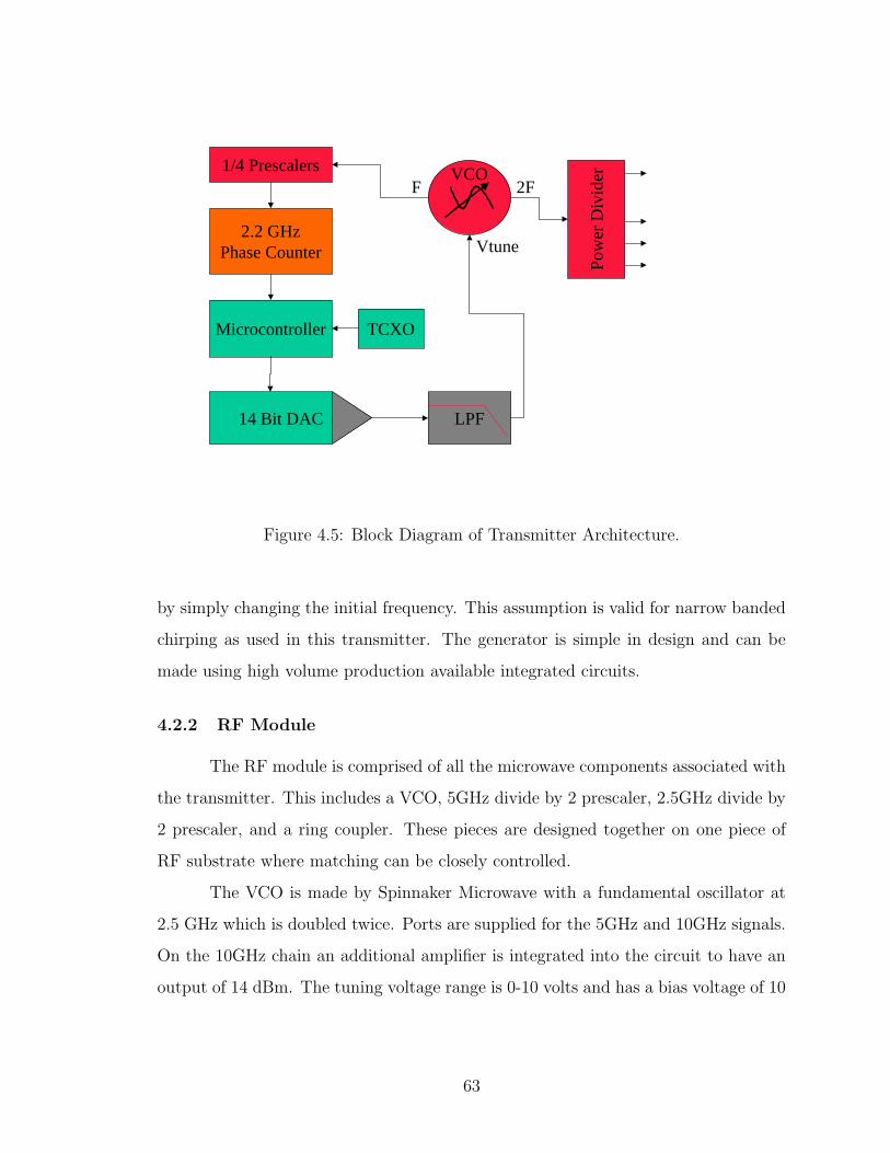
Microcontroller
1/4 Prescalers
2.2 GHzPhase Counter
LPF14 Bit DAC
Pow
er D
ivid
er
2FF
Vtune
TCXO
VCO
Figure 4.5: Block Diagram of Transmitter Architecture.
by simply changing the initial frequency. This assumption is valid for narrow banded
chirping as used in this transmitter. The generator is simple in design and can be
made using high volume production available integrated circuits.
4.2.2 RF Module
The RF module is comprised of all the microwave components associated with
the transmitter. This includes a VCO, 5GHz divide by 2 prescaler, 2.5GHz divide by
2 prescaler, and a ring coupler. These pieces are designed together on one piece of
RF substrate where matching can be closely controlled.
The VCO is made by Spinnaker Microwave with a fundamental oscillator at
2.5 GHz which is doubled twice. Ports are supplied for the 5GHz and 10GHz signals.
On the 10GHz chain an additional amplifier is integrated into the circuit to have an
output of 14 dBm. The tuning voltage range is 0-10 volts and has a bias voltage of 10
63
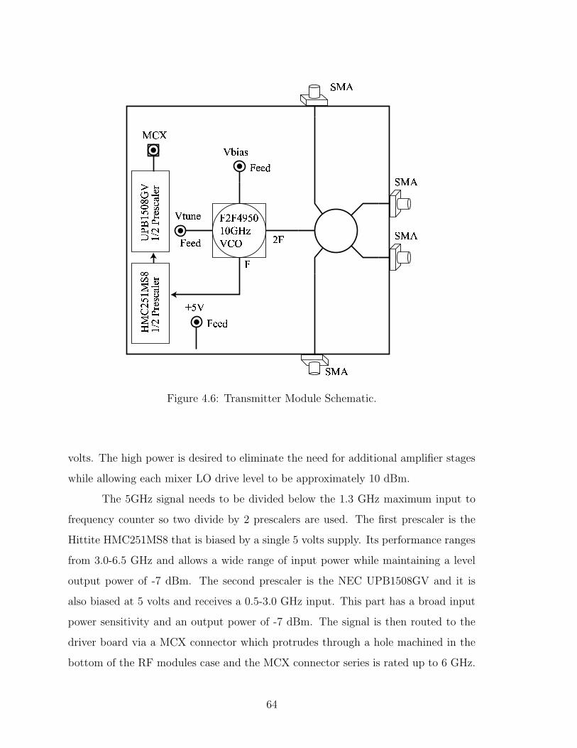
! #"%$&('*)
+
&-,/.1032
&-465+7/8
9:<;
9:=;
9:=;
9!:=;
: '?>
@BACACD
@ A ACD
@BACACDE 3&
Figure 4.6: Transmitter Module Schematic.
volts. The high power is desired to eliminate the need for additional amplifier stages
while allowing each mixer LO drive level to be approximately 10 dBm.
The 5GHz signal needs to be divided below the 1.3 GHz maximum input to
frequency counter so two divide by 2 prescalers are used. The first prescaler is the
Hittite HMC251MS8 that is biased by a single 5 volts supply. Its performance ranges
from 3.0-6.5 GHz and allows a wide range of input power while maintaining a level
output power of -7 dBm. The second prescaler is the NEC UPB1508GV and it is
also biased at 5 volts and receives a 0.5-3.0 GHz input. This part has a broad input
power sensitivity and an output power of -7 dBm. The signal is then routed to the
driver board via a MCX connector which protrudes through a hole machined in the
bottom of the RF modules case and the MCX connector series is rated up to 6 GHz.
64
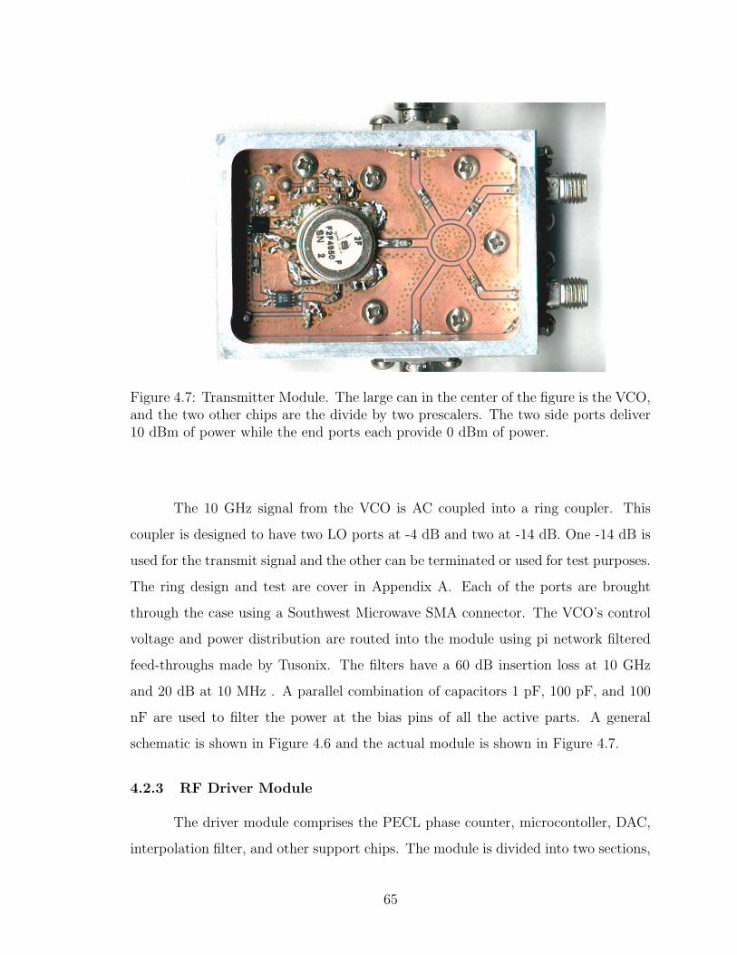
Figure 4.7: Transmitter Module. The large can in the center of the figure is the VCO,and the two other chips are the divide by two prescalers. The two side ports deliver10 dBm of power while the end ports each provide 0 dBm of power.
The 10 GHz signal from the VCO is AC coupled into a ring coupler. This
coupler is designed to have two LO ports at -4 dB and two at -14 dB. One -14 dB is
used for the transmit signal and the other can be terminated or used for test purposes.
The ring design and test are cover in Appendix A. Each of the ports are brought
through the case using a Southwest Microwave SMA connector. The VCO’s control
voltage and power distribution are routed into the module using pi network filtered
feed-throughs made by Tusonix. The filters have a 60 dB insertion loss at 10 GHz
and 20 dB at 10 MHz . A parallel combination of capacitors 1 pF, 100 pF, and 100
nF are used to filter the power at the bias pins of all the active parts. A general
schematic is shown in Figure 4.6 and the actual module is shown in Figure 4.7.
4.2.3 RF Driver Module
The driver module comprises the PECL phase counter, microcontoller, DAC,
interpolation filter, and other support chips. The module is divided into two sections,
65
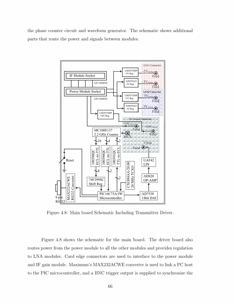
the phase counter circuit and waveform generator. The schematic shows additional
parts that route the power and signals between modules.
Figure 4.8: Main board Schematic Including Transmitter Driver.
Figure 4.8 shows the schematic for the main board. The driver board also
routes power from the power module to all the other modules and provides regulation
to LNA modules. Card edge connectors are used to interface to the power module
and IF gain module. Maximum’s MAX232ACWE converter is used to link a PC host
to the PIC microcontroller, and a BNC trigger output is supplied to synchronize the
66
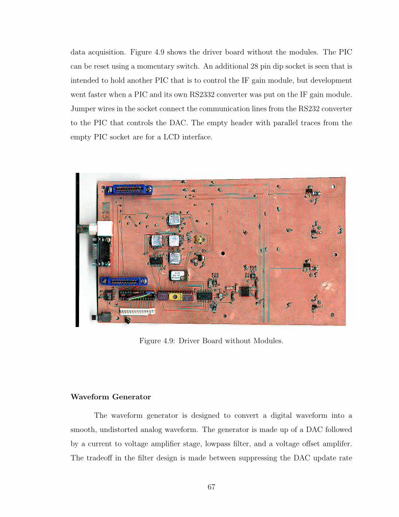
data acquisition. Figure 4.9 shows the driver board without the modules. The PIC
can be reset using a momentary switch. An additional 28 pin dip socket is seen that is
intended to hold another PIC that is to control the IF gain module, but development
went faster when a PIC and its own RS2332 converter was put on the IF gain module.
Jumper wires in the socket connect the communication lines from the RS232 converter
to the PIC that controls the DAC. The empty header with parallel traces from the
empty PIC socket are for a LCD interface.
Figure 4.9: Driver Board without Modules.
Waveform Generator
The waveform generator is designed to convert a digital waveform into a
smooth, undistorted analog waveform. The generator is made up of a DAC followed
by a current to voltage amplifier stage, lowpass filter, and a voltage offset amplifer.
The tradeoff in the filter design is made between suppressing the DAC update rate
67
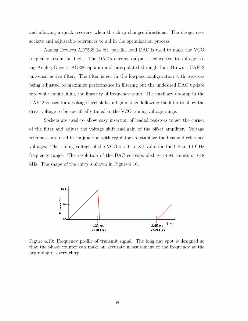
and allowing a quick recovery when the chirp changes directions. The design uses
sockets and adjustable references to aid in the optimization process.
Analog Devices AD7538 14 bit, parallel load DAC is used to make the VCO
frequency resolution high. The DAC’s current output is converted to voltage us-
ing Analog Devices AD820 op-amp and interpolated through Burr Brown’s UAF42
universal active filter. The filter is set in the lowpass configuration with resistors
being adjusted to maximize performance in filtering out the undesired DAC update
rate while maintaining the linearity of frequency ramp. The auxillary op-amp in the
UAF42 is used for a voltage level shift and gain stage following the filter to allow the
drive voltage to be specifically tuned to the VCO tuning voltage range.
Sockets are used to allow easy insertion of leaded resistors to set the corner
of the filter and adjust the voltage shift and gain of the offset amplifier. Voltage
references are used in conjunction with regulators to stabilize the bias and reference
voltages. The tuning voltage of the VCO is 5.6 to 8.1 volts for the 9.8 to 10 GHz
frequency range. The resolution of the DAC corresponded to 14.84 counts or 618
kHz. The shape of the chirp is shown in Figure 4.10.
"!$#&%
' (*) +*-,"!$#.%
/1032 0
452 6
452 4
Figure 4.10: Frequency profile of transmit signal. The long flat spot is designed sothat the phase counter can make an accurate measurement of the frequency at thebeginning of every chirp.
68
Phase Counter Circuit
The phase counter accurately measures the output of the VCO by the use of
high speed logic and a counter in the PIC microcontroller. This measurement is used
to determine an array of digital values, that when sent to the DAC create a linear
frequency output from the VCO.
The phase counter circuit consists of a PECL counter, PECL-TTL translation
chips, a shift register and a PIC microcontroller. A short overview of Emitter Coupled
Logic (ECL) is included in Appendix F to aid understanding in the workings of the
PECL parts. The MC100E137 is a high speed, 8-bit ripple counter that can handle
clock speeds up to 2.2 GHz. The counter is able to count a 1.25 GHz signal at a
power level of -10 dBm by using the AC coupling scheme as shown in Appendix F.
CMOS or TTL level translation devices are necessary to interface with the chip. The
two different Fairchild devices used are the 100390 ECL to TTL translator and the
100391 TTL to ECL translator. Power supply conversions, shown in the Appendix,
are required to operate the devices as PECL devices where they run on a positive 5
volt supply.
A carefully designed 5 volt and 3 volt power plane ensures successful operation
of PECL devices that tend to draw a lot of current and are sensitive to noise. The chips
are placed close together to minimize transmission line effects at high speeds. The 3
volt supply is used to terminate the transmission lines so the amount of the energy
consumed by the circuit is reduced. The PIC16C173A microcontroller is clocked
at 20 MHz with a TCXO. A shift register is used to load the bits from the phase
counter into the PIC to reduce the I/O support. The most significant bit from the
MC100E137 is routed into a 16 bit counter in the PIC.
4.2.4 Algorithms and Control Code
The hardware has been described that generates the LFM signal and now the
digital waveform generation in code is explained. Some processing for the calibration
routine is carried out on the PC because the PIC is an 8 bit processor with limited
69
resources. Here the calibration algorithm is shown in detail, and the rest of the code
is left to be examined as it is in the Appendix.
Figure 4.11 shows the flow diagram for the algorithm used to calibrate the
transmitter. A static calibration loop in the microcontroller sets the DAC to a prede-
termined voltage and then measures the response of the VCO. The value from the PIC
and PECL counters are sent to the PC where it compares the measured frequency to
a desired frequency, and then adjusts the voltage accordingly. The adjusted voltage
is sent back to the PIC where it loads the DAC, and again measures the frequency.
It will repeat the process until the measured and desired frequencies match. This
process is repeated for a linear array of desired frequencies.
The run mode follows a similar pattern by stepping through the array and
loading the DAC in a timed sequence. A trigger pulse is generated to synchronize
the transmitter with the digitizer. When the end of the array is reached, the PIC
loads the start value for the chirp and then measures the output frequency. The array
offset is adjusted if the measured initial frequency is out of range. The relative array
is then run through once again. The ability to measure the initial frequency on each
pass during transmission and correct for any error, makes the transmitter calibration
quasi dynamic.
Because of the limited resources of the PIC, the Visual Basic Executable con-
verts constants such as bandwidth, initial frequency, and channel gain into parameters
used by the PIC. The Visual Basic user interface is shown in Figure 4.12. The radar’s
transmit frequency is strongly dependent on temperature and requires a warm up
period. The strip chart shown at the bottom of the screen shot plots the frequency
as a function of time. When the frequency stabilizes, the transmitter is ready for
calibration. Debug functions include frequency counting, selectable voltage output,
communication test, and calibration feedback. The code for both the PIC and the
executable are included in the Appendix.
70
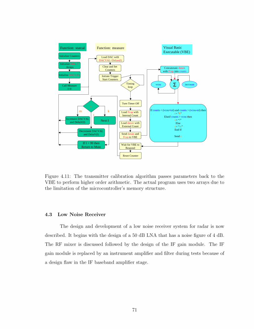
Initialize Delta V Arrays
Initialize Counters Load DAC with DACVAL+Deltav(I)
Turn Timer Off
Initiate TriggerStart Counters
Clear and Set Counters
Initialize DACVAL
Call MeasureI=0
Function: measureFunction: statcal
Timingloop
Load Fcap with Internal Count
Load datain withExternal Count
Send datain andFcap to VBE
Wait for VBE toRespond
Reset Counter
Concatenate datainwith Fcap into counts
Visual BasicExecutable (VBE)
Σvcou inccount
If counts < (vcou+tol) and counts > (vcou-tol) thenc= “k”
Elseif counts > vcou thenc= “ l”Else
c= “m” End If
Send c
c
Next IIncrement DACVAL
and DeltaV(I)
Decrement DACVALand DeltaV(I)
k1
m
If I > 99 thenReturn to Main
Figure 4.11: The transmitter calibration algorithm passes parameters back to theVBE to perform higher order arithmetic. The actual program uses two arrays due tothe limitation of the microcontroller’s memory structure.
4.3 Low Noise Receiver
The design and development of a low noise receiver system for radar is now
described. It begins with the design of a 50 dB LNA that has a noise figure of 4 dB.
The RF mixer is discussed followed by the design of the IF gain module. The IF
gain module is replaced by an instrument amplifier and filter during tests because of
a design flaw in the IF baseband amplifier stage.
71
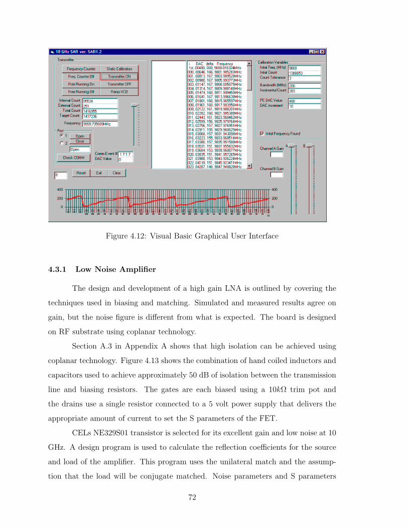
Figure 4.12: Visual Basic Graphical User Interface
4.3.1 Low Noise Amplifier
The design and development of a high gain LNA is outlined by covering the
techniques used in biasing and matching. Simulated and measured results agree on
gain, but the noise figure is different from what is expected. The board is designed
on RF substrate using coplanar technology.
Section A.3 in Appendix A shows that high isolation can be achieved using
coplanar technology. Figure 4.13 shows the combination of hand coiled inductors and
capacitors used to achieve approximately 50 dB of isolation between the transmission
line and biasing resistors. The gates are each biased using a 10kΩ trim pot and
the drains use a single resistor connected to a 5 volt power supply that delivers the
appropriate amount of current to set the S parameters of the FET.
CELs NE329S01 transistor is selected for its excellent gain and low noise at 10
GHz. A design program is used to calculate the reflection coefficients for the source
and load of the amplifier. This program uses the unilateral match and the assump-
tion that the load will be conjugate matched. Noise parameters and S parameters
72
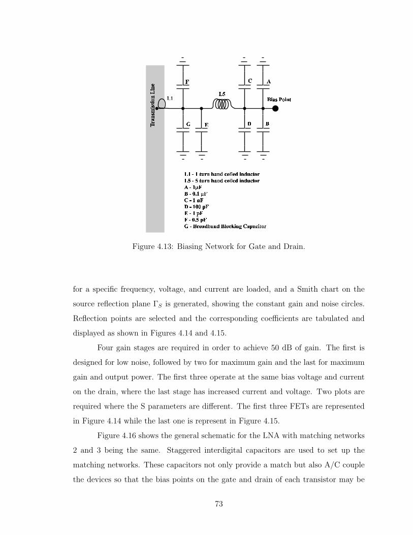
!"#%$'&(*)+ ,.-*/( 0 1(-2 '-.$./3 4& 5!67%$'&(*)+ ,.-*/( 0 1(-2 '-.$./3 4& !"489!6:4; <8 !7'=!,:4:5>' !"#>.?!@:4; 5>. !+ &3A -B@ .-C0 4/(D' .E F>@ /3 4&
Figure 4.13: Biasing Network for Gate and Drain.
for a specific frequency, voltage, and current are loaded, and a Smith chart on the
source reflection plane ΓS is generated, showing the constant gain and noise circles.
Reflection points are selected and the corresponding coefficients are tabulated and
displayed as shown in Figures 4.14 and 4.15.
Four gain stages are required in order to achieve 50 dB of gain. The first is
designed for low noise, followed by two for maximum gain and the last for maximum
gain and output power. The first three operate at the same bias voltage and current
on the drain, where the last stage has increased current and voltage. Two plots are
required where the S parameters are different. The first three FETs are represented
in Figure 4.14 while the last one is represent in Figure 4.15.
Figure 4.16 shows the general schematic for the LNA with matching networks
2 and 3 being the same. Staggered interdigital capacitors are used to set up the
matching networks. These capacitors not only provide a match but also A/C couple
the devices so that the bias points on the gate and drain of each transistor may be
73
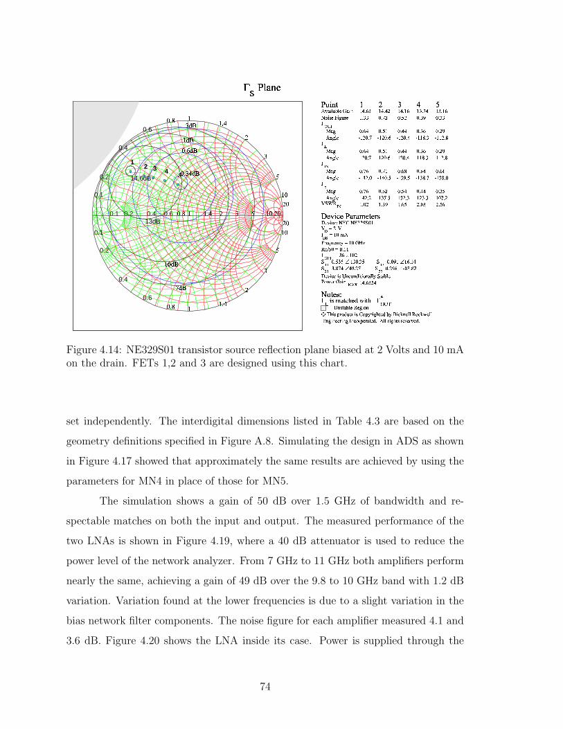
0.1 0.2 0.4 0.6 0.1
0.2
0.4
0.6
0.1
0.2
0.4
0.6
13dB
14.6dB
! #" $&%')(+* , - * .+- /0)* , 12#34, 5 /6, 7 849 /:;+<=>?* 7')1+74- /:@ >?* 7')1+74- /:A B >?* 7')1+74- /:C >?* 7')1+74- /D#E4FHG A BIKJLM" NJOQPRPSTJ% JRUV&/ (+, W /4X 2&YZQ2&Y[ \4]4E^_D`Ma!\bDc ` C)a?_ ^)dM'69 / e 84/ 1+W f&a?_ ^&0hg&iG1 j k ^)a!^+l _4_: ;+m = aQl [4nho_ ^4\Ehp pb^l k [+kMoq _ [4^+l [+krEhp st^+l ^4]_)o!_ n4l _ uEs pb[l v w uo&u4]l \4w Es sx^+l \ ]+nMoyq v [+l v \V&/ (+, W /h, 5z)14W 3 1+ , | , 3 1+* - - fME+| * .+- /3 ~&/ 90&* , 1b _ ul n [+k u )% JhU&b &O4 4? # z#
z)15 | * .- /G/ 74, 3 1O4, 5+9 3 84W |, 5Z3 4f49 , 7 4| / h.+f&h, W 1+/ - -4G34W 4~&/ - -Y1474, 1+/ / 9 , 1+7&c 1+W 3 9 +/ 9 * | / l'&- -49 , 7 | 59 / 5 / 9 (+/ +l
1
_ l [4[_ ul n [
^+l n uq _ \4^l w^+l n u_ \4^l w^+l w+nq _ u+\l ^
_ l ^4\^+l w+n_ u+\l \
2
^l w \_ ul u+\
^l k_q _ \ ^l n^l k__ \ ^l n^l w_q _ u4^l k
_ l [ ]^l n \_ [ wl k
3
^l k \_ ul _ n
^l u4uq _ \ ^l u^l u4u_ \ ^l u^l n4vq _ [ ]l k
_ l n4k^l k u_ [ \l [
4
^l [ ]_ [l w u
^l [4nq _4_ v4l [^l [4n_4_ v4l [^l n uq _ [+v4l w
\l ^ [^l u u_ \4[+l [
^l [ [_ [+l _ n
^l \ ]q _4_ \l v^l \ ]_4_ \l v^l n_q _ [4v+l ^
\l k n^l [4k_ ^ wl \
Figure 4.14: NE329S01 transistor source reflection plane biased at 2 Volts and 10 mAon the drain. FETs 1,2 and 3 are designed using this chart.
set independently. The interdigital dimensions listed in Table 4.3 are based on the
geometry definitions specified in Figure A.8. Simulating the design in ADS as shown
in Figure 4.17 showed that approximately the same results are achieved by using the
parameters for MN4 in place of those for MN5.
The simulation shows a gain of 50 dB over 1.5 GHz of bandwidth and re-
spectable matches on both the input and output. The measured performance of the
two LNAs is shown in Figure 4.19, where a 40 dB attenuator is used to reduce the
power level of the network analyzer. From 7 GHz to 11 GHz both amplifiers perform
nearly the same, achieving a gain of 49 dB over the 9.8 to 10 GHz band with 1.2 dB
variation. Variation found at the lower frequencies is due to a slight variation in the
bias network filter components. The noise figure for each amplifier measured 4.1 and
3.6 dB. Figure 4.20 shows the LNA inside its case. Power is supplied through the
74
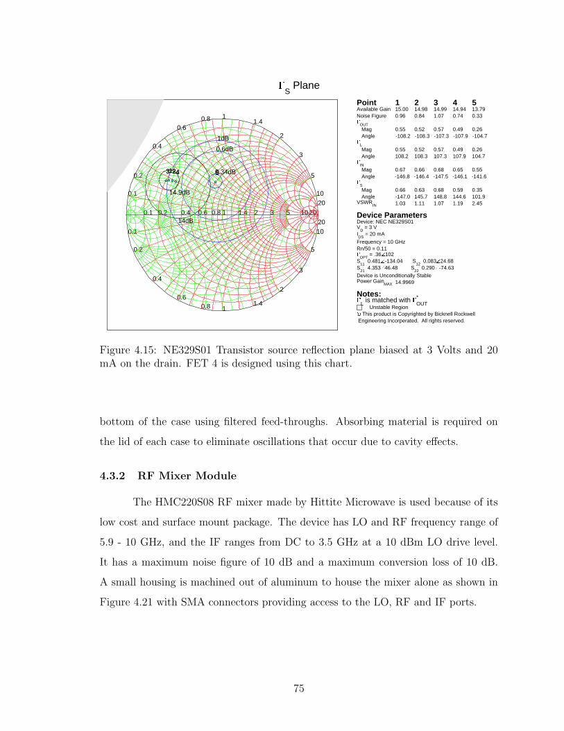
S Plane
0.1 0.2 0.4 0.6 0.8 1 1.4 2 3 5 10 20
0.1
0.2
0.4
0.6 0.8 1
1.4
2
3
5
10 20
0.1
0.2
0.4
0.6 0.8 1
1.4
2
3
5
10 20
14dB
14.9dB
0.34dB
0.6dB
1dB
Point Available Gain Noise Figure
OUT Mag Angle
L Mag Angle
IN Mag Angle
S Mag Angle
VSWR IN
Device Parameters Device: NEC NE329S01 V
D = 3 V
I DS
= 20 mA
Frequency = 10 GHz Rn/50 = 0.11
OPT = .36 102
S 11
0.481 -134.04 S 12
0.083 24.68 S
21 4.353 46.48 S
22 0.290 -74.63
Device is Unconditionally Stable Power Gain
MAX 14.9969
Notes: L is matched with
OUT *
Unstable Region This product is Copyrighted by Bicknell Rockwell
Engineering Incorperated. All rights reserved.
1
1
0.96 15.00
0.55 -108.2
0.55 108.2
0.67 -146.8
1.03
0.66 -147.0
2
2
0.84 14.98
0.52 -108.3
0.52 108.3
0.66 -146.4
1.11
0.63 145.7
3
3
1.07 14.99
0.57 -107.3
0.57 107.3
0.68 -147.5
1.07
0.68 148.8
4
4
0.74 14.94
0.49 -107.9
0.49 107.9
0.65 -146.1
1.19
0.59 144.6
5
5
0.33 13.79
0.26 -104.7
0.26 104.7
0.55 -141.6
2.45
0.35 101.9
Figure 4.15: NE329S01 Transistor source reflection plane biased at 3 Volts and 20mA on the drain. FET 4 is designed using this chart.
bottom of the case using filtered feed-throughs. Absorbing material is required on
the lid of each case to eliminate oscillations that occur due to cavity effects.
4.3.2 RF Mixer Module
The HMC220S08 RF mixer made by Hittite Microwave is used because of its
low cost and surface mount package. The device has LO and RF frequency range of
5.9 - 10 GHz, and the IF ranges from DC to 3.5 GHz at a 10 dBm LO drive level.
It has a maximum noise figure of 10 dB and a maximum conversion loss of 10 dB.
A small housing is machined out of aluminum to house the mixer alone as shown in
Figure 4.21 with SMA connectors providing access to the LO, RF and IF ports.
75
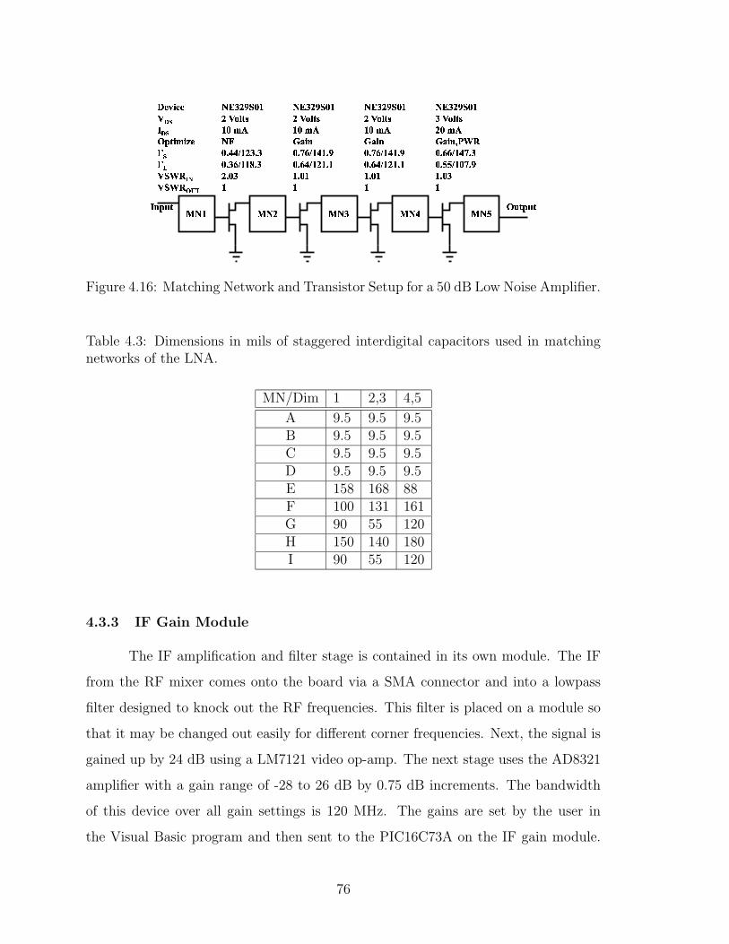
!"$#%&(' *) +-,/.0 1132 450 0 32 350 30 (
67 !3"$#80 (2 40 0 132 93:0 0 (
67 !3"$#%&(' 0 5132 430 0 1((2 430 30
!3"$#%&(' 0 5132 430 0 1((2 430 30
;< = ' > <6?@A?@* ' " ' B <C @C-D,E.F G,E.6HI(J
Figure 4.16: Matching Network and Transistor Setup for a 50 dB Low Noise Amplifier.
Table 4.3: Dimensions in mils of staggered interdigital capacitors used in matchingnetworks of the LNA.
MN/Dim 1 2,3 4,5
A 9.5 9.5 9.5B 9.5 9.5 9.5C 9.5 9.5 9.5D 9.5 9.5 9.5E 158 168 88F 100 131 161G 90 55 120H 150 140 180I 90 55 120
4.3.3 IF Gain Module
The IF amplification and filter stage is contained in its own module. The IF
from the RF mixer comes onto the board via a SMA connector and into a lowpass
filter designed to knock out the RF frequencies. This filter is placed on a module so
that it may be changed out easily for different corner frequencies. Next, the signal is
gained up by 24 dB using a LM7121 video op-amp. The next stage uses the AD8321
amplifier with a gain range of -28 to 26 dB by 0.75 dB increments. The bandwidth
of this device over all gain settings is 120 MHz. The gains are set by the user in
the Visual Basic program and then sent to the PIC16C73A on the IF gain module.
76
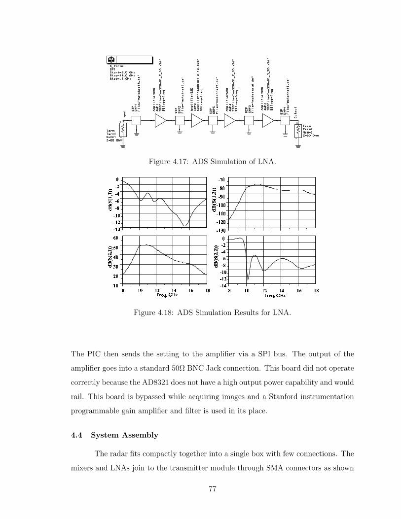
Figure 4.17: ADS Simulation of LNA.
!""
# $%# $&# $'# (# )# %# &'
*+,-,./.00
132451326513225132551 751 851 95
:;<=<>?@AA
B CD CE CF CG CBH CFH CEH CDH BH GH FH ED
IJKLMNPORQ
STUVU WXWYY
Figure 4.18: ADS Simulation Results for LNA.
The PIC then sends the setting to the amplifier via a SPI bus. The output of the
amplifier goes into a standard 50Ω BNC Jack connection. This board did not operate
correctly because the AD8321 does not have a high output power capability and would
rail. This board is bypassed while acquiring images and a Stanford instrumentation
programmable gain amplifier and filter is used in its place.
4.4 System Assembly
The radar fits compactly together into a single box with few connections. The
mixers and LNAs join to the transmitter module through SMA connectors as shown
77
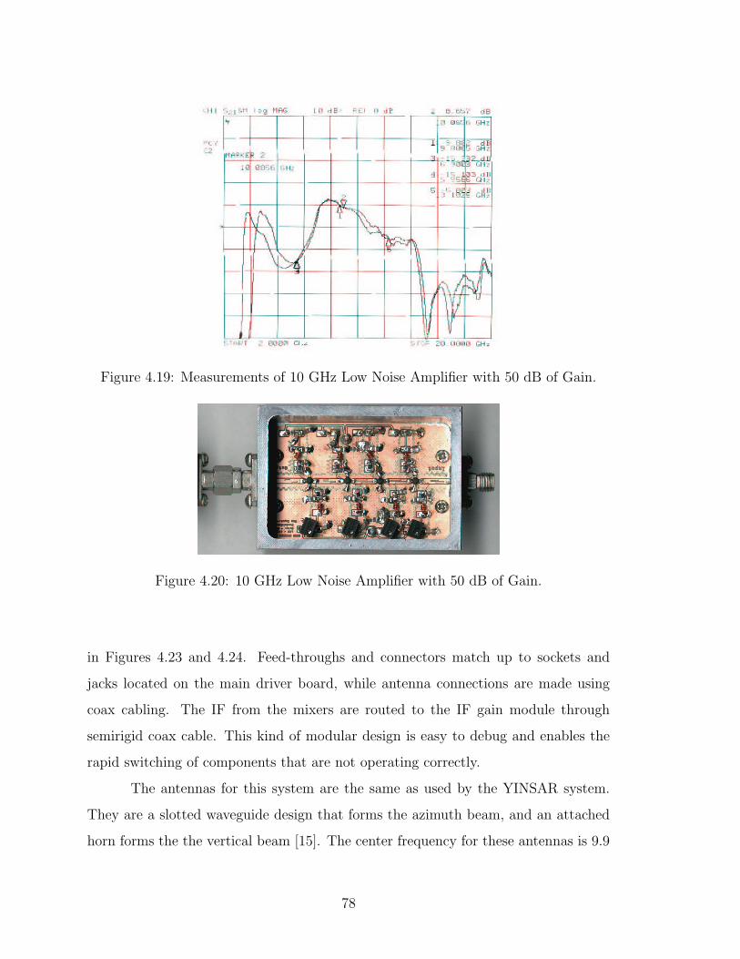
Figure 4.19: Measurements of 10 GHz Low Noise Amplifier with 50 dB of Gain.
Figure 4.20: 10 GHz Low Noise Amplifier with 50 dB of Gain.
in Figures 4.23 and 4.24. Feed-throughs and connectors match up to sockets and
jacks located on the main driver board, while antenna connections are made using
coax cabling. The IF from the mixers are routed to the IF gain module through
semirigid coax cable. This kind of modular design is easy to debug and enables the
rapid switching of components that are not operating correctly.
The antennas for this system are the same as used by the YINSAR system.
They are a slotted waveguide design that forms the azimuth beam, and an attached
horn forms the the vertical beam [15]. The center frequency for these antennas is 9.9
78
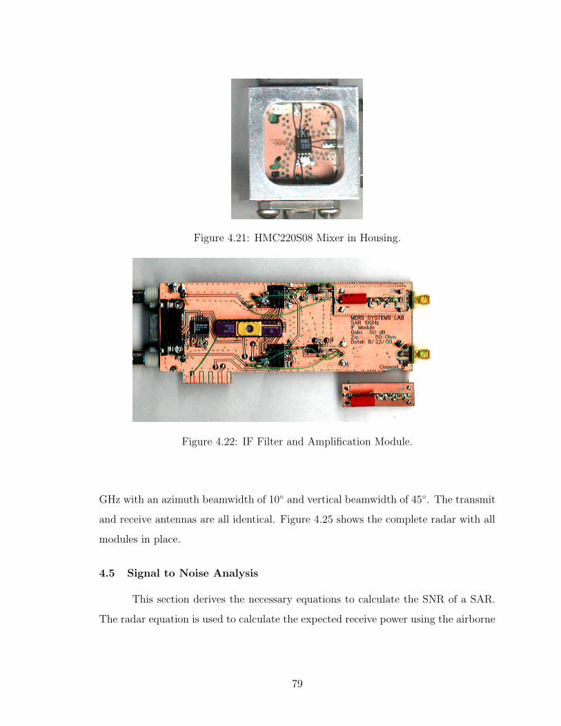
Figure 4.21: HMC220S08 Mixer in Housing.
Figure 4.22: IF Filter and Amplification Module.
GHz with an azimuth beamwidth of 10 and vertical beamwidth of 45. The transmit
and receive antennas are all identical. Figure 4.25 shows the complete radar with all
modules in place.
4.5 Signal to Noise Analysis
This section derives the necessary equations to calculate the SNR of a SAR.
The radar equation is used to calculate the expected receive power using the airborne
79
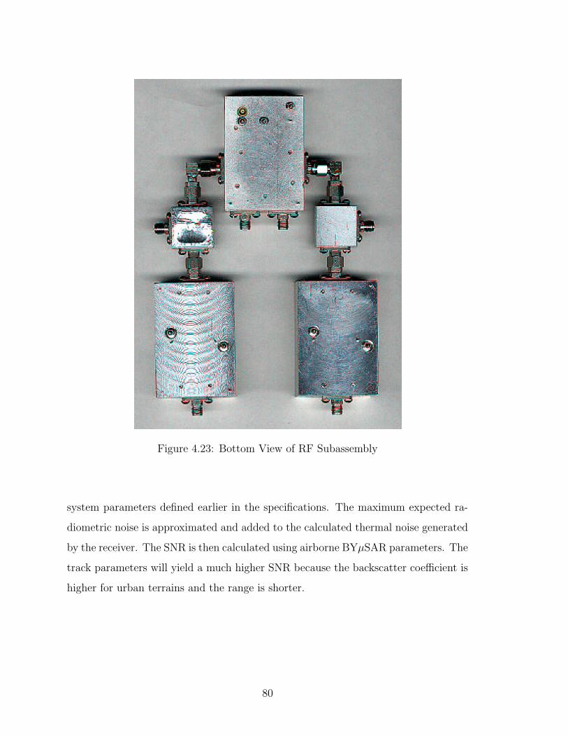
Figure 4.23: Bottom View of RF Subassembly
system parameters defined earlier in the specifications. The maximum expected ra-
diometric noise is approximated and added to the calculated thermal noise generated
by the receiver. The SNR is then calculated using airborne BYµSAR parameters. The
track parameters will yield a much higher SNR because the backscatter coefficient is
higher for urban terrains and the range is shorter.
80
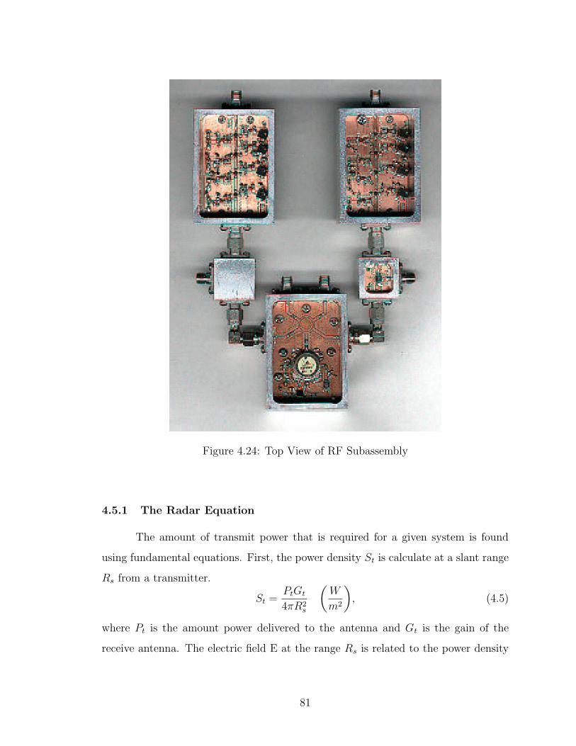
Figure 4.24: Top View of RF Subassembly
4.5.1 The Radar Equation
The amount of transmit power that is required for a given system is found
using fundamental equations. First, the power density St is calculate at a slant range
Rs from a transmitter.
St =PtGt
4πR2s
(
W
m2
)
, (4.5)
where Pt is the amount power delivered to the antenna and Gt is the gain of the
receive antenna. The electric field E at the range Rs is related to the power density
81
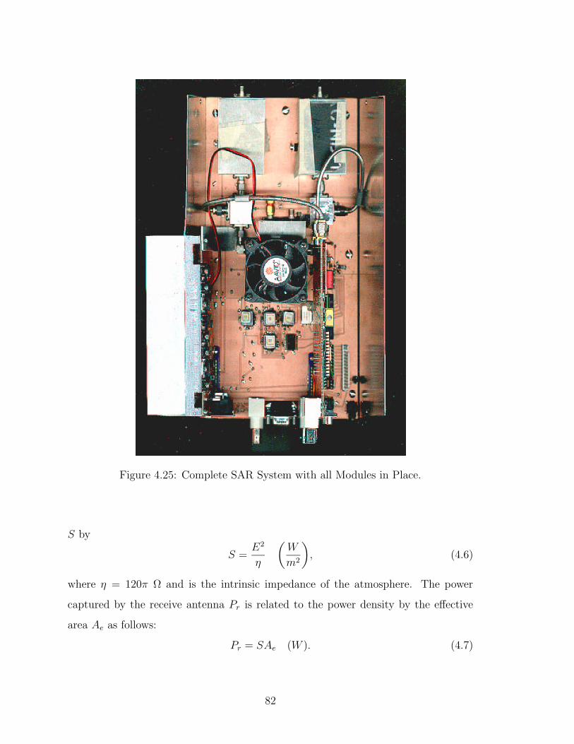
Figure 4.25: Complete SAR System with all Modules in Place.
S by
S =E2
η
(
W
m2
)
, (4.6)
where η = 120π Ω and is the intrinsic impedance of the atmosphere. The power
captured by the receive antenna Pr is related to the power density by the effective
area Ae as follows:
Pr = SAe (W ). (4.7)
82

This effective area is also related to gain of the receive antenna Gr and the carrier
wavelength λ by
Ae =λ2Gr
4π(m2). (4.8)
In a microwave communications link the power received Pr is related to the
power transmitted Pt by the Friis power transmission Equation [38]
Pr = PtGtGrλ
2
(4πRs)2, (4.9)
Here the antenna mismatch is not included, and it is assumed that the antennas are
polarized with each other. This is also assuming a non-obstructed path for the signal
to travel through the air[1].
The radar equation changes slightly. A given target in the field will capture
some of the energy and then reradiate it in all directions. The amount that is radi-
ated in a given direction will be a function of the target’s material composition and
geometrical shape and size. It is called the radar cross section σ, but the surface
scattering coefficient σ is commonly used for terrain classification and it is related
to σ by
σ = σAres, (4.10)
where Ares is the product of the azimuth and range resolution size.
There is imposed another loss range loss term 1/4πR2s because the signal is
reradiated which results in a received power of
Pr =PtGtGrλ
2σAres(4π)3R4s
. (4.11)
The received power Pr is the amount of power delivered to the receiver from the
antenna. σ is the quantity that is to be measured, and a range of values can vary from
-25dB to 20dB. The other variables in Equation 4.11 are system design parameters.
The amount of radiometric and thermal noise that is expected in the system must be
calculated in order to determine the amount of transmit power needed. The physics
of the system must be examined and the necessary assumptions stated that will
83
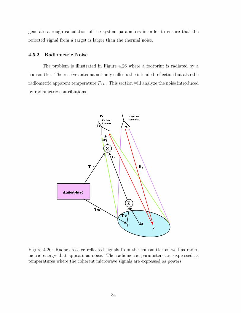
generate a rough calculation of the system parameters in order to ensure that the
reflected signal from a target is larger than the thermal noise.
4.5.2 Radiometric Noise
The problem is illustrated in Figure 4.26 where a footprint is radiated by a
transmitter. The receive antenna not only collects the intended reflection but also the
radiometric apparent temperature TAP . This section will analyze the noise introduced
by radiometric contributions.
"!#
%$'&( )
*%+
-,
.0/132 46587#9#7
:
;
;
Figure 4.26: Radars receive reflected signals from the transmitter as well as radio-metric energy that appears as noise. The radiometric parameters are expressed astemperatures where the coherent microwave signals are expressed as powers.
84
The total noise power at the input of the receiver PNi,Tot is expressed as a
function of temperature
PNi,Tot = kB(TA + TTL + LTLTrec), (4.12)
where TA is the detectable antenna temperature, TTL is the effective temperature of a
lossy transmission line, LTL is the loss of the line, and Trec is the effective temperature
of the receiver as seen at it input. B is the noise bandwidth and k is Boltzmann’s
constant. The detectable antenna temperature is related to the antenna efficiency ηl,
the apparent temperature TAP , and the antenna’s physical temperature Tp by
TA = ηlTAP + (1− ηl)Tp. (4.13)
The transmission line temperature is related to its physical temperature TP and its
loss by
TTL = (L− 1)TP . (4.14)
The apparent temperature TAP as seen by the antenna is given by
TAP =1
La[TB + TSC ] + TUP . (4.15)
The loss term La is a function of frequency and distance. This term is expected to be
negligible and will be assumed to be 1 at a 10 km range and 10 GHz. The brightness
temperature TB is related to the actual temperature of the ground T and emissivity
e by
TB(θ, φ, f) = Te(θ, φ, f). (4.16)
The emissivity ranges from 0.2 to 1 when the incident angle is between 45 and 65.
The emissivity can be set to 1 by assuming the worst case. 50C can be assumed as
the hottest ground temperature.
The next term is called the downwelling scattered brightness TSC , and repre-
sents the portion of radiation impinging on the surface from the upper atmosphere.
85
TUP is the upward emitted radiation due to the atmosphere. By assuming a lossless
atmosphere both of these terms become negligible and are set to 0.
Equation 4.13 is simplified to
TA = ηlT + (1− ηl)Tp. (4.17)
The noise power delivered by the antenna P ′A to the receiver is represented by
P ′A = k[ηlT + (1− ηl)Tp]B, (4.18)
4.5.3 Thermal Noise
The last contribution to PNi,Tot is by the receiver itself. Electrons within
conductors are in a state of random motion which generates variations in voltage. This
variation is called thermal noise. Trec is calculated by knowing the noise temperature
of each of the receiver subsystems. The noise temperature for the receiver is then
calculated, and then the total noise power is defined for the system.
A common measurement of thermal noise is noise figure F defined as
F =Psi/PniPso/Pno
, (4.19)
=SNRin
SNRout
. (4.20)
The noise figure is defined by having the input to the receiver matched, and the
matching element at 290K. It can then be related to the equivalent noise tempera-
ture by
T = (F − 1)To, (4.21)
where To = 290K.
86
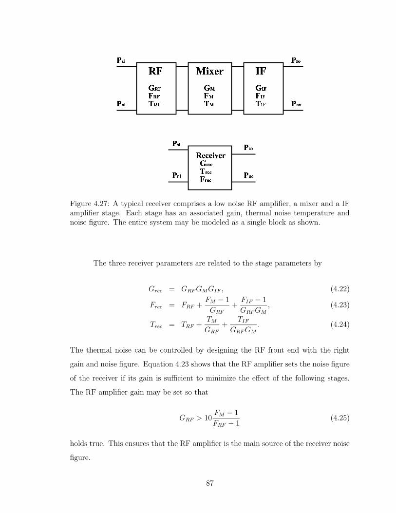
"!$#&% !'#&% !$#&%
(*),+).-&/ )0
1 2
12
32
2
Figure 4.27: A typical receiver comprises a low noise RF amplifier, a mixer and a IFamplifier stage. Each stage has an associated gain, thermal noise temperature andnoise figure. The entire system may be modeled as a single block as shown.
The three receiver parameters are related to the stage parameters by
Grec = GRFGMGIF , (4.22)
Frec = FRF +FM − 1
GRF
+FIF − 1
GRFGM
, (4.23)
Trec = TRF +TMGRF
+TIF
GRFGM
. (4.24)
The thermal noise can be controlled by designing the RF front end with the right
gain and noise figure. Equation 4.23 shows that the RF amplifier sets the noise figure
of the receiver if its gain is sufficient to minimize the effect of the following stages.
The RF amplifier gain may be set so that
GRF > 10FM − 1
FRF − 1(4.25)
holds true. This ensures that the RF amplifier is the main source of the receiver noise
figure.
87

The total noise power at the receiver’s input can be found given that the
noise figure of each device is known along with the physical temperatures. The
noise bandwidth B is determined by the RF bandwidth. The SNR is determined
by using the time-bandwidth product T · BW as processing gain [28]. The thermal
and radiometric noise is cancelled due to their randomness. The radar signal is
coherent and therefore experiences no cancellation. This is also true for the azimuth
compression and can be represented by twice the value of no(R) as defined in Equation
3.76. The output signal to noise ratio becomes
SNRout =PrT ·BW2no
PNi,Tot. (4.26)
4.5.4 SNR Calculations
The expected SNR for the airborne system can now be calculated using the
parameters listed in Table 4.1 with an elevation of 600 m.
Pr =PtGtGrλ
2σ∆R∆a
(4π)3R4(4.27)
where Rmin and σmax are used for maximum SNR and Rmax and σmin for minimum
SNR.
Pr,min = −2dBm+ 17dB + 17dB − 25dB + 10log10
(
∆Rmax∆a
(4π)3R4s,max
)
, (4.28)
= −161dBm, (4.29)
Pr,max = −2dBm+ 17dB + 17dB + 20dB + 10log10
(
∆Rmin∆a
(4π)3R4s,min
)
, (4.30)
= −108dBm. (4.31)
88

The processing gain for both azimuth and range compression is found by
PGT = T ·BW2no (4.32)
= 10, 000θaR
vT(4.33)
PGT,Rmin = 74dB, (4.34)
PGT,Rmax = 76dB. (4.35)
The noise temperature of the receiver is
Trec = TRF +TMGRF
+TIF
GRFGM
, (4.36)
= 435 +9(290)
100, 000+
9(290)
10, 000, (4.37)
≈ 435, (4.38)
which shows that the noise is dominated by the noise figure of the RF amplifier. The
total noise power at the input of the receiver is
PNi,Tot = kBW (TA + TTL + LTLTrec), (4.39)
= 1.38× 10−23200× 106(323K + (1.6− 1)290K + 696K), (4.40)
= −84.8dBm. (4.41)
89

The signal to noise ratio is the sum of the received power from the radar signal and
the processing gain minus the noise power expressed in dB as follows:
SNRout = Pr + PG− PNi,Tot, (4.42)
SNRout,min = Pr,min + PGT,Rmax − PNi,Tot, (4.43)
= −161dBm+ 76dB + 84.8dBm, (4.44)
= −0.2dBm, (4.45)
SNRout,max = Pr,max + PGT,Rmin − PNi,Tot, (4.46)
= −108dBm+ 74dB + 84.8dBm, (4.47)
= 50.8dB. (4.48)
Either the maximum range or the range of the backscatter coefficient will be limited
by using the parameters chosen.
90
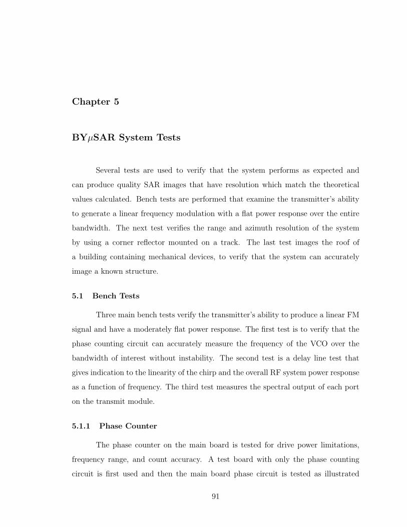
Chapter 5
BYµSAR System Tests
Several tests are used to verify that the system performs as expected and
can produce quality SAR images that have resolution which match the theoretical
values calculated. Bench tests are performed that examine the transmitter’s ability
to generate a linear frequency modulation with a flat power response over the entire
bandwidth. The next test verifies the range and azimuth resolution of the system
by using a corner reflector mounted on a track. The last test images the roof of
a building containing mechanical devices, to verify that the system can accurately
image a known structure.
5.1 Bench Tests
Three main bench tests verify the transmitter’s ability to produce a linear FM
signal and have a moderately flat power response. The first test is to verify that the
phase counting circuit can accurately measure the frequency of the VCO over the
bandwidth of interest without instability. The second test is a delay line test that
gives indication to the linearity of the chirp and the overall RF system power response
as a function of frequency. The third test measures the spectral output of each port
on the transmit module.
5.1.1 Phase Counter
The phase counter on the main board is tested for drive power limitations,
frequency range, and count accuracy. A test board with only the phase counting
circuit is first used and then the main board phase circuit is tested as illustrated
91
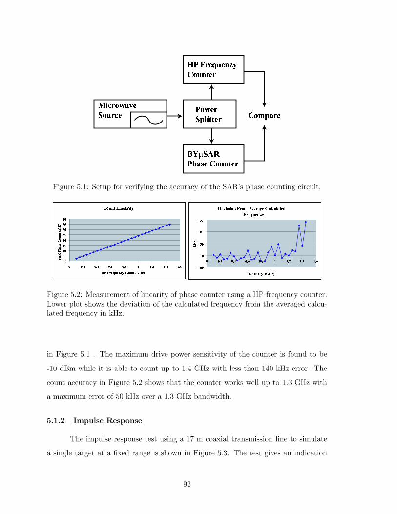
"! ##$#%'&()#
*,+-%#/.0/12'%3
/.0#5467+89 (:;4<=#
Figure 5.1: Setup for verifying the accuracy of the SAR’s phase counting circuit.
>@?7ACBEDGF)H BEIKJ8L H D M
NOP NPOQ NQOR NROS N
N N T QUNVT SWN T XYNVT Z P P T Q[P T S\P T X]9^@_8` a bdcda edf gihCj cdeKk7l mn]9o p
qr stu vwxy z|~
I GH JD H ?7B#LV?8GIdLVJ88I)>J KAC J7D IKiLKIK-AnIVBEVM
ONNONP N NPON
N N T QN T SWN T XWN T Z P P T QP T S[P T X
_8` a bdcKaVeKf g/l mn]9o p
Figure 5.2: Measurement of linearity of phase counter using a HP frequency counter.Lower plot shows the deviation of the calculated frequency from the averaged calcu-lated frequency in kHz.
in Figure 5.1 . The maximum drive power sensitivity of the counter is found to be
-10 dBm while it is able to count up to 1.4 GHz with less than 140 kHz error. The
count accuracy in Figure 5.2 shows that the counter works well up to 1.3 GHz with
a maximum error of 50 kHz over a 1.3 GHz bandwidth.
5.1.2 Impulse Response
The impulse response test using a 17 m coaxial transmission line to simulate
a single target at a fixed range is shown in Figure 5.3. The test gives an indication
92
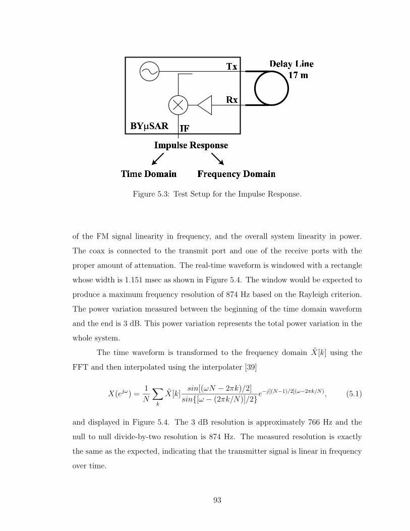
"!
#%$
# !'&)( *%+,* &- *.
/ ! -! 0 $/1,2 ( ,34 -! 0
Figure 5.3: Test Setup for the Impulse Response.
of the FM signal linearity in frequency, and the overall system linearity in power.
The coax is connected to the transmit port and one of the receive ports with the
proper amount of attenuation. The real-time waveform is windowed with a rectangle
whose width is 1.151 msec as shown in Figure 5.4. The window would be expected to
produce a maximum frequency resolution of 874 Hz based on the Rayleigh criterion.
The power variation measured between the beginning of the time domain waveform
and the end is 3 dB. This power variation represents the total power variation in the
whole system.
The time waveform is transformed to the frequency domain X[k] using the
FFT and then interpolated using the interpolater [39]
X(ejω) =1
N
∑
k
X[k]sin[(ωN − 2πk)/2]
sin[ω − (2πk/N)]/2e−j[(N−1)/2](ω−2πk/N), (5.1)
and displayed in Figure 5.4. The 3 dB resolution is approximately 766 Hz and the
null to null divide-by-two resolution is 874 Hz. The measured resolution is exactly
the same as the expected, indicating that the transmitter signal is linear in frequency
over time.
93
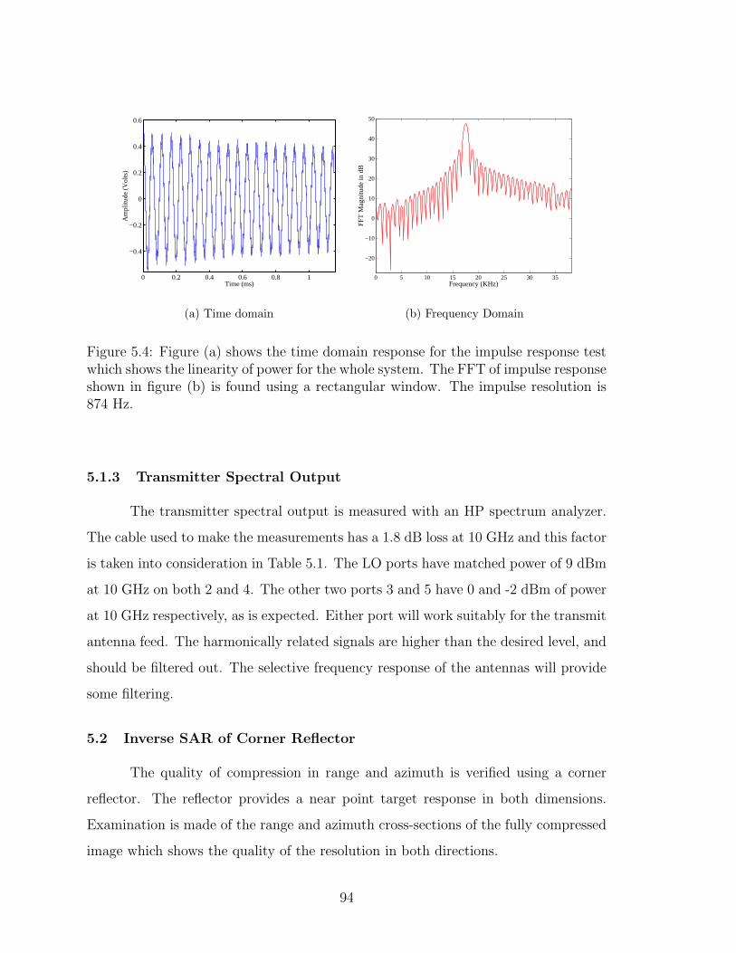
0 0.2 0.4 0.6 0.8 1
−0.4
−0.2
0
0.2
0.4
0.6
Time (ms)
Am
plitu
de (
Vol
ts)
(a) Time domain
0 5 10 15 20 25 30 35
−20
−10
0
10
20
30
40
50
Frequency (KHz)
FFT
Mag
nitu
de in
dB
(b) Frequency Domain
Figure 5.4: Figure (a) shows the time domain response for the impulse response testwhich shows the linearity of power for the whole system. The FFT of impulse responseshown in figure (b) is found using a rectangular window. The impulse resolution is874 Hz.
5.1.3 Transmitter Spectral Output
The transmitter spectral output is measured with an HP spectrum analyzer.
The cable used to make the measurements has a 1.8 dB loss at 10 GHz and this factor
is taken into consideration in Table 5.1. The LO ports have matched power of 9 dBm
at 10 GHz on both 2 and 4. The other two ports 3 and 5 have 0 and -2 dBm of power
at 10 GHz respectively, as is expected. Either port will work suitably for the transmit
antenna feed. The harmonically related signals are higher than the desired level, and
should be filtered out. The selective frequency response of the antennas will provide
some filtering.
5.2 Inverse SAR of Corner Reflector
The quality of compression in range and azimuth is verified using a corner
reflector. The reflector provides a near point target response in both dimensions.
Examination is made of the range and azimuth cross-sections of the fully compressed
image which shows the quality of the resolution in both directions.
94
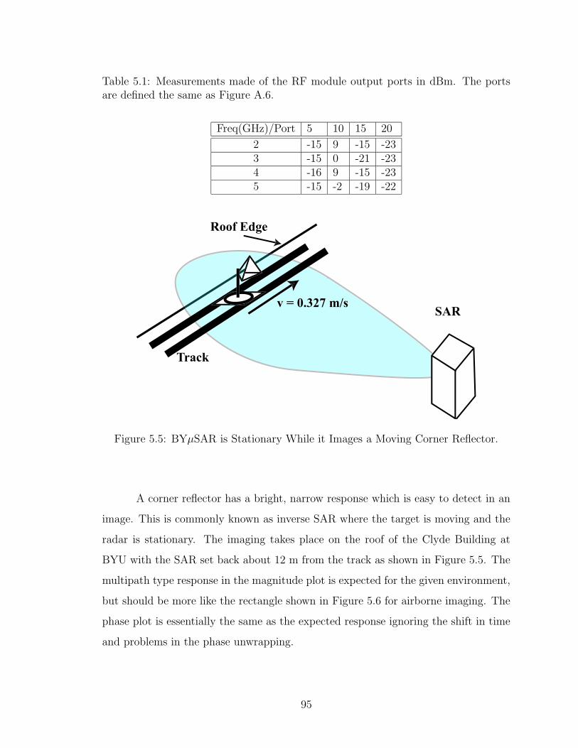
Table 5.1: Measurements made of the RF module output ports in dBm. The portsare defined the same as Figure A.6.
Freq(GHz)/Port 5 10 15 20
2 -15 9 -15 -233 -15 0 -21 -234 -16 9 -15 -235 -15 -2 -19 -22
Figure 5.5: BYµSAR is Stationary While it Images a Moving Corner Reflector.
A corner reflector has a bright, narrow response which is easy to detect in an
image. This is commonly known as inverse SAR where the target is moving and the
radar is stationary. The imaging takes place on the roof of the Clyde Building at
BYU with the SAR set back about 12 m from the track as shown in Figure 5.5. The
multipath type response in the magnitude plot is expected for the given environment,
but should be more like the rectangle shown in Figure 5.6 for airborne imaging. The
phase plot is essentially the same as the expected response ignoring the shift in time
and problems in the phase unwrapping.
95
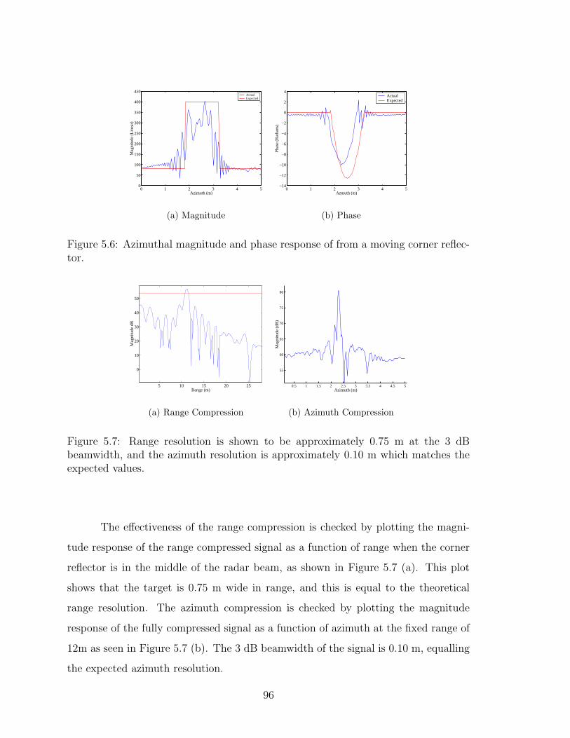
0 1 2 3 4 50
50
100
150
200
250
300
350
400
450
Azimuth (m)
Mag
nitu
de (
Lin
ear)
ActualExpected
(a) Magnitude
0 1 2 3 4 5−14
−12
−10
−8
−6
−4
−2
0
2
4
Azmuth (m)
Pha
se (
Rad
ians
)
ActualExpected
(b) Phase
Figure 5.6: Azimuthal magnitude and phase response of from a moving corner reflec-tor.
5 10 15 20 25
0
10
20
30
40
50
Range (m)
Mag
nitu
de d
B
(a) Range Compression
0.5 1 1.5 2 2.5 3 3.5 4 4.5 5
55
60
65
70
75
80
Azimuth (m)
Mag
nitu
de (
dB)
(b) Azimuth Compression
Figure 5.7: Range resolution is shown to be approximately 0.75 m at the 3 dBbeamwidth, and the azimuth resolution is approximately 0.10 m which matches theexpected values.
The effectiveness of the range compression is checked by plotting the magni-
tude response of the range compressed signal as a function of range when the corner
reflector is in the middle of the radar beam, as shown in Figure 5.7 (a). This plot
shows that the target is 0.75 m wide in range, and this is equal to the theoretical
range resolution. The azimuth compression is checked by plotting the magnitude
response of the fully compressed signal as a function of azimuth at the fixed range of
12m as seen in Figure 5.7 (b). The 3 dB beamwidth of the signal is 0.10 m, equalling
the expected azimuth resolution.
96
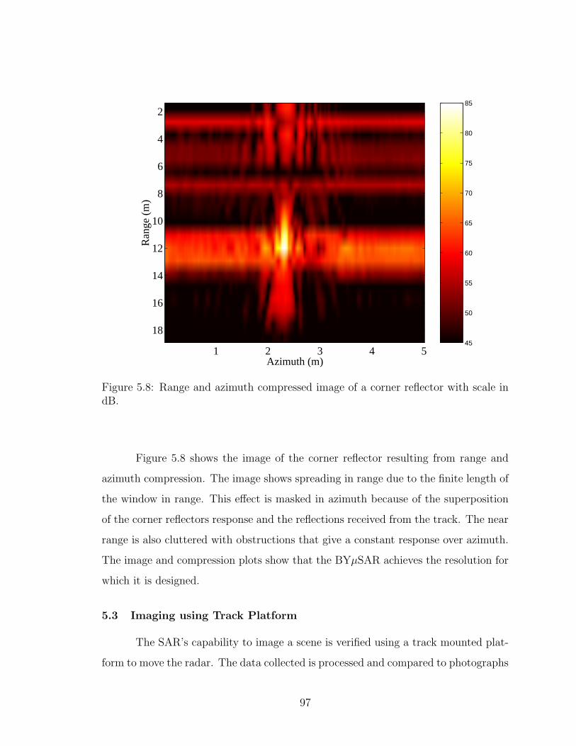
45
50
55
60
65
70
75
80
85
Azimuth (m)
Ran
ge (
m)
1 2 3 4 5
2
4
6
8
10
12
14
16
18
Figure 5.8: Range and azimuth compressed image of a corner reflector with scale indB.
Figure 5.8 shows the image of the corner reflector resulting from range and
azimuth compression. The image shows spreading in range due to the finite length of
the window in range. This effect is masked in azimuth because of the superposition
of the corner reflectors response and the reflections received from the track. The near
range is also cluttered with obstructions that give a constant response over azimuth.
The image and compression plots show that the BYµSAR achieves the resolution for
which it is designed.
5.3 Imaging using Track Platform
The SAR’s capability to image a scene is verified using a track mounted plat-
form to move the radar. The data collected is processed and compared to photographs
97
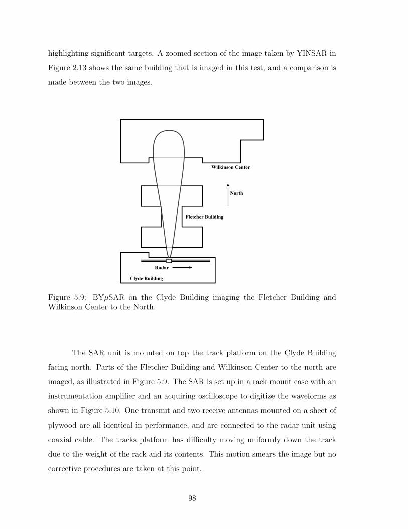
highlighting significant targets. A zoomed section of the image taken by YINSAR in
Figure 2.13 shows the same building that is imaged in this test, and a comparison is
made between the two images.
Figure 5.9: BYµSAR on the Clyde Building imaging the Fletcher Building andWilkinson Center to the North.
The SAR unit is mounted on top the track platform on the Clyde Building
facing north. Parts of the Fletcher Building and Wilkinson Center to the north are
imaged, as illustrated in Figure 5.9. The SAR is set up in a rack mount case with an
instrumentation amplifier and an acquiring oscilloscope to digitize the waveforms as
shown in Figure 5.10. One transmit and two receive antennas mounted on a sheet of
plywood are all identical in performance, and are connected to the radar unit using
coaxial cable. The tracks platform has difficulty moving uniformly down the track
due to the weight of the rack and its contents. This motion smears the image but no
corrective procedures are taken at this point.
98
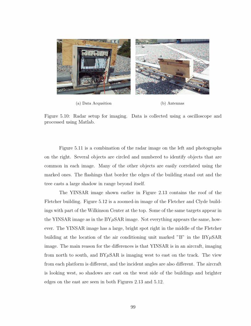
(a) Data Acqusition (b) Antennas
Figure 5.10: Radar setup for imaging. Data is collected using a oscilloscope andprocessed using Matlab.
Figure 5.11 is a combination of the radar image on the left and photographs
on the right. Several objects are circled and numbered to identify objects that are
common in each image. Many of the other objects are easily correlated using the
marked ones. The flashings that border the edges of the building stand out and the
tree casts a large shadow in range beyond itself.
The YINSAR image shown earlier in Figure 2.13 contains the roof of the
Fletcher building. Figure 5.12 is a zoomed-in image of the Fletcher and Clyde build-
ings with part of the Wilkinson Center at the top. Some of the same targets appear in
the YINSAR image as in the BYµSAR image. Not everything appears the same, how-
ever. The YINSAR image has a large, bright spot right in the middle of the Fletcher
building at the location of the air conditioning unit marked ”B” in the BYµSAR
image. The main reason for the differences is that YINSAR is in an aircraft, imaging
from north to south, and BYµSAR is imaging west to east on the track. The view
from each platform is different, and the incident angles are also different. The aircraft
is looking west, so shadows are cast on the west side of the buildings and brighter
edges on the east are seen in both Figures 2.13 and 5.12.
99
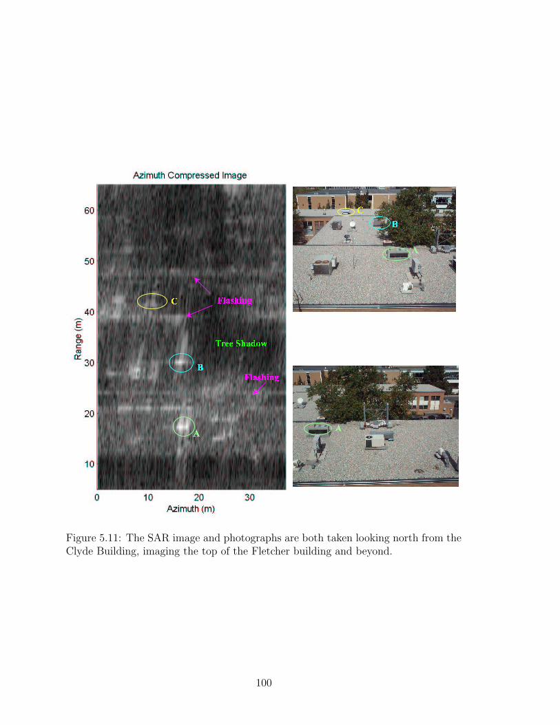
Figure 5.11: The SAR image and photographs are both taken looking north from theClyde Building, imaging the top of the Fletcher building and beyond.
100
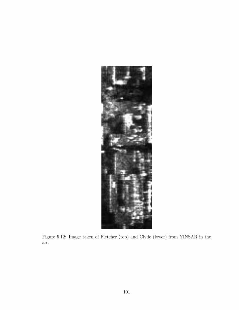
Figure 5.12: Image taken of Fletcher (top) and Clyde (lower) from YINSAR in theair.
101

102
Chapter 6
Conclusion
In conclusion, it has been shown that the BYµSAR project is successful in de-
veloping new technologies that will affect the SAR community. Recommendations are
given for the improvement of the SAR sensor and for microwave circuit development
in a research setting. The contributions made by this thesis are then given.
6.1 Summary
BYµSAR is an innovative system developed on the success of three other SAR
projects at BYU. It is the first SAR of its cost, size, weight, and power consumption to
be developed which has excellent resolution. The use of FM/CW range compression
in a SAR application makes this work unique. The transmit power is very low because
it is compensated by the large processing gain achieved using a long chirp period. The
signal is already compressed before it is digitized, reducing the cost and complexity of
the digital acquisition. This thesis has addressed the question: What effects are found
in compression due to using FM/CW techniques? It is shown that an increased linear
shift in range walk occurs and an equation to solve for the shifted amount is given. In
addition, it is proved that no phase errors are introduced within the specified bounds
of operation.
A 10 GHz prototype unit is designed and built to validate these claims. The
prototype’s linear chirp waveform generator uses a novel technique in generating a
quasi dynamic frequency to voltage mapping digitally. The system is successfully
fabricated using coplanar technology that enables compact circuit design at high
frequencies. Part of the research is to develop methods that allowed accurate design
103
of coplanar microwave circuits. A test fixture is built, and procedures are developed
that make precise measurements of coplanar circuits possible.
The system design is composed of small module blocks that can be switched,
making debugging easy. The entire unit fits compactly into a single box and is powered
by a +/- 12 volt supply. Analysis is made on the system’s SNR and shows that its
specifications would allow excellent terrain mapping. The bench tests performed show
that the radar has excellent linearity and a flat power response.
It is shown by using a corner reflector that the range and azimuth resolution
of the prototype match the design specifications. A SAR image is also made of a
building, and has good detail and contrast supporting that quality images can be
expected from an airborne system.
6.2 Future Work
The radar system could be further reduced in size and complexity with ex-
pected advances in the development of microwave circuits on ICs. The IF gain
module needs to be redesigned in conjunction with the design of a compact data
acquisition system with a large memory storage capacity. The system could then be
flown aboard an aircraft and larger data sets could be collected to further verify the
system’s performance.
In-flight processing should also be pursued by using a digital signal processing
technology. Memory space for raw data is the same size as that of a processed im-
age, making processing an attractive option for realtime image realization. Motion
compensation should be studied for this type of system, and then the appropriate
algorithms can be used to remove degenerate motion effects. This would allow the
use of data while the instrument is imaging. Planar array antennas should be man-
ufactured to increase compactness of the system and increase its reliability. These
arrays would form fit into the skins or hull of a miniature aircraft making it suitable
for use on UAVs.
It is recommended that a specification be made and followed for the develop-
ment of future microwave sensors that allow the modulation type, center frequency
104

and bandwidth of systems to be easily changed or modified without the expense of a
complete system redesign. This would reduce development cost and time. It would
also increase quality, reliability, and flexibility of prototyping microwave sensors.
6.3 Contributions
The work in this thesis introduces a new technique and sensor for SAR imaging.
It is proved that within limits, FM/CW SAR introduces no azimuth phase errors, but
increases a linear shift to range walk. A simple LFM signal generator is designed and
developed that showed good linearity and fair frequency stability that finds use in
several other systems at Brigham Young University.
Techniques to design and/make innovative coplanar circuits using relatively
inexpensive equipment are developed. A high gain LNA is achieved using a low cost
PCB substrate, and this gives confidence for the design of other technical building
blocks of microwave circuits. The development of a modular style design is initiated
where parts like the driver circuit could be reused in other designs helping to eliminate
unnecessary design cost and effort.
105

106

Appendix A
Channelized Coplanar Waveguide Technology
Coplanar waveguide technology produces effective isolation, allows simple con-
ductor geometries to realize fundamental circuit elements, and facilitates simple com-
ponent placement. Coplanar is not used extensively in circuit design because of the
difficultly in analyzing its behavior. This appendix will show an approach to devel-
oping circuits using coplanar technology. It begins with a discussion on its benefits,
followed by the design of a 50Ω line, DC isolation circuits, basic elements. The final
section covers the tools used for fabrication and issues in board design.
A.1 Coplanar’s Benefits
Conductor Backed Coplanar Waveguide (CBCPW) is chosen to develop the
main board and modules due to its strong confinement of electromagnetic energy and
its ability to provide easy shunt and series part placement [40, 41]. A Finite Difference
Time Domain (FDTD) solution is shown in Figure A.1. FDTD only considers the
static field and does not include the energy found in parallel plate or waveguide modes.
Channelized Coplanar Waveguide (CCPW) is realized by creating vias between the
bottom and top conductors [42]. Parallel plate and rectangular waveguide modes
within the dielectric are eliminated by choosing the position of the vias properly.
Parallel plate wave modes also exist in microstrip due to the boundary created by the
dielectric and air, which allows waves to propagate in the substrate. This contributes
to transmission loss and crosstalk between lines. A large percentage of the energy
in CPW transmission lines propagate in the slot mode, and this further reduces the
amount of radiated energy into the air.
107
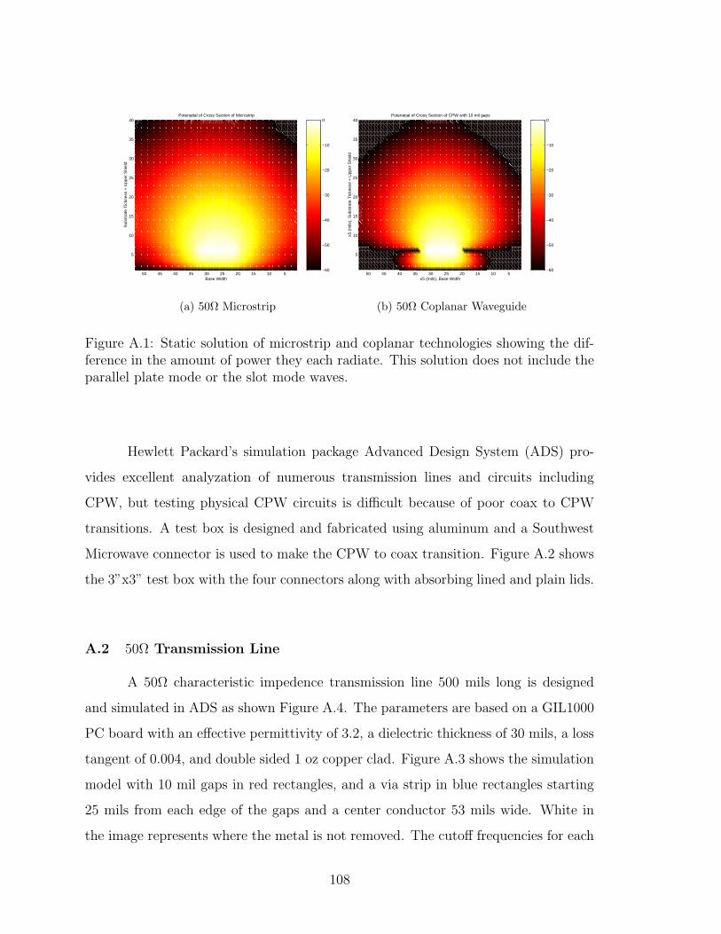
−60
−50
−40
−30
−20
−10
0
5
10
15
20
25
30
35
40
5101520253035404550
Potenatial of Cross Section of Microstrip
Base Width
Sub
stra
te T
ickn
ess
+ U
pper
Shi
eld
(a) 50Ω Microstrip
−60
−50
−40
−30
−20
−10
0
5
10
15
20
25
30
35
40
5101520253035404550
Potenatial of Cross Section of CPW with 10 mil gaps
x5 (mils), Base Width
x5 (
mils
), S
ubst
rate
Tic
knes
s +
Upp
er S
hiel
d
(b) 50Ω Coplanar Waveguide
Figure A.1: Static solution of microstrip and coplanar technologies showing the dif-ference in the amount of power they each radiate. This solution does not include theparallel plate mode or the slot mode waves.
Hewlett Packard’s simulation package Advanced Design System (ADS) pro-
vides excellent analyzation of numerous transmission lines and circuits including
CPW, but testing physical CPW circuits is difficult because of poor coax to CPW
transitions. A test box is designed and fabricated using aluminum and a Southwest
Microwave connector is used to make the CPW to coax transition. Figure A.2 shows
the 3”x3” test box with the four connectors along with absorbing lined and plain lids.
A.2 50Ω Transmission Line
A 50Ω characteristic impedence transmission line 500 mils long is designed
and simulated in ADS as shown Figure A.4. The parameters are based on a GIL1000
PC board with an effective permittivity of 3.2, a dielectric thickness of 30 mils, a loss
tangent of 0.004, and double sided 1 oz copper clad. Figure A.3 shows the simulation
model with 10 mil gaps in red rectangles, and a via strip in blue rectangles starting
25 mils from each edge of the gaps and a center conductor 53 mils wide. White in
the image represents where the metal is not removed. The cutoff frequencies for each
108
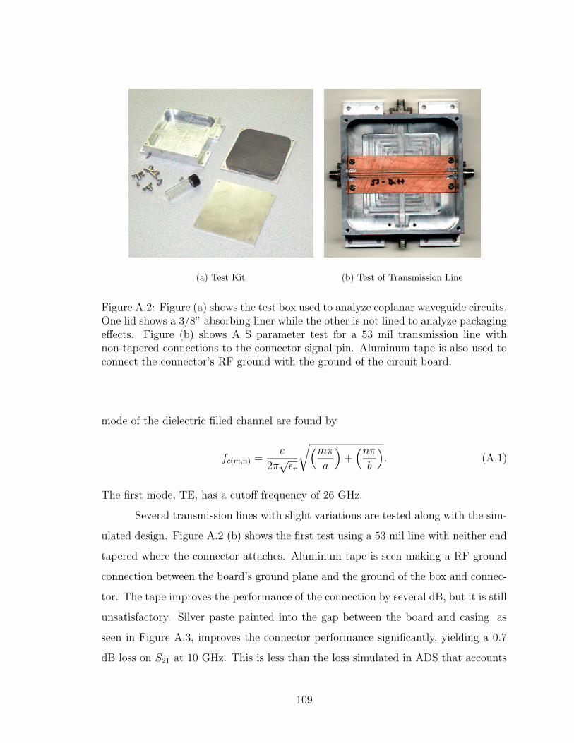
(a) Test Kit (b) Test of Transmission Line
Figure A.2: Figure (a) shows the test box used to analyze coplanar waveguide circuits.One lid shows a 3/8” absorbing liner while the other is not lined to analyze packagingeffects. Figure (b) shows A S parameter test for a 53 mil transmission line withnon-tapered connections to the connector signal pin. Aluminum tape is also used toconnect the connector’s RF ground with the ground of the circuit board.
mode of the dielectric filled channel are found by
fc(m,n) =c
2π√εr
√
(mπ
a
)
+(nπ
b
)
. (A.1)
The first mode, TE, has a cutoff frequency of 26 GHz.
Several transmission lines with slight variations are tested along with the sim-
ulated design. Figure A.2 (b) shows the first test using a 53 mil line with neither end
tapered where the connector attaches. Aluminum tape is seen making a RF ground
connection between the board’s ground plane and the ground of the box and connec-
tor. The tape improves the performance of the connection by several dB, but it is still
unsatisfactory. Silver paste painted into the gap between the board and casing, as
seen in Figure A.3, improves the connector performance significantly, yielding a 0.7
dB loss on S21 at 10 GHz. This is less than the loss simulated in ADS that accounts
109
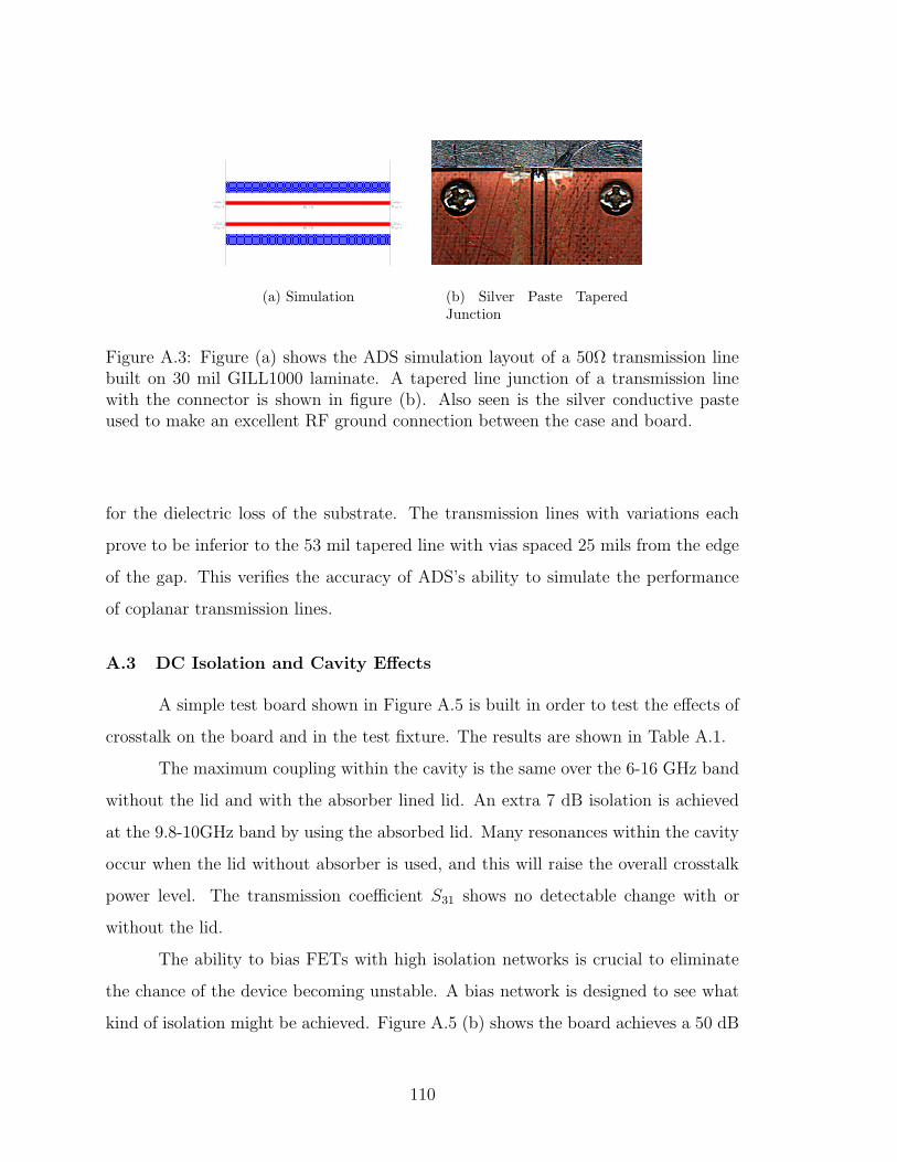
(a) Simulation (b) Silver Paste TaperedJunction
Figure A.3: Figure (a) shows the ADS simulation layout of a 50Ω transmission linebuilt on 30 mil GILL1000 laminate. A tapered line junction of a transmission linewith the connector is shown in figure (b). Also seen is the silver conductive pasteused to make an excellent RF ground connection between the case and board.
for the dielectric loss of the substrate. The transmission lines with variations each
prove to be inferior to the 53 mil tapered line with vias spaced 25 mils from the edge
of the gap. This verifies the accuracy of ADS’s ability to simulate the performance
of coplanar transmission lines.
A.3 DC Isolation and Cavity Effects
A simple test board shown in Figure A.5 is built in order to test the effects of
crosstalk on the board and in the test fixture. The results are shown in Table A.1.
The maximum coupling within the cavity is the same over the 6-16 GHz band
without the lid and with the absorber lined lid. An extra 7 dB isolation is achieved
at the 9.8-10GHz band by using the absorbed lid. Many resonances within the cavity
occur when the lid without absorber is used, and this will raise the overall crosstalk
power level. The transmission coefficient S31 shows no detectable change with or
without the lid.
The ability to bias FETs with high isolation networks is crucial to eliminate
the chance of the device becoming unstable. A bias network is designed to see what
kind of isolation might be achieved. Figure A.5 (b) shows the board achieves a 50 dB
110
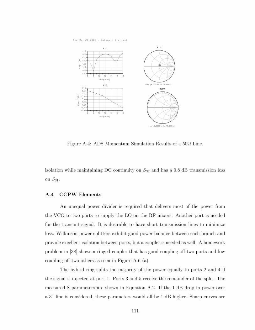
Figure A.4: ADS Momentum Simulation Results of a 50Ω Line.
isolation while maintaining DC continuity on S32 and has a 0.8 dB transmission loss
on S31.
A.4 CCPW Elements
An unequal power divider is required that delivers most of the power from
the VCO to two ports to supply the LO on the RF mixers. Another port is needed
for the transmit signal. It is desirable to have short transmission lines to minimize
loss. Wilkinson power splitters exhibit good power balance between each branch and
provide excellent isolation between ports, but a coupler is needed as well. A homework
problem in [38] shows a ringed coupler that has good coupling off two ports and low
coupling off two others as seen in Figure A.6 (a).
The hybrid ring splits the majority of the power equally to ports 2 and 4 if
the signal is injected at port 1. Ports 3 and 5 receive the remainder of the split. The
measured S parameters are shown in Equation A.2. If the 1 dB drop in power over
a 3” line is considered, these parameters would all be 1 dB higher. Sharp curves are
111
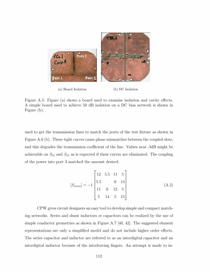
(a) Board Isolation (b) DC Isolation
Figure A.5: Figure (a) shows a board used to examine isolation and cavity effects.A simple board used to achieve 50 dB isolation on a DC bias network is shown inFigure (b).
used to get the transmission lines to match the ports of the test fixture as shown in
Figure A.6 (b). These tight curves cause phase mismatches between the coupled slots,
and this degrades the transmission coefficient of the line. Values near -3dB might be
achievable on S21 and S41 as is expected if these curves are eliminated. The coupling
of the power into port 3 matched the amount desired.
[Smeas] = −1
12 5.5 11 5
5.5 6 14
11 6 12 5
5 14 5 15
(A.2)
CPW gives circuit designers an easy tool to develop simple and compact match-
ing networks. Series and shunt inductors or capacitors can be realized by the use of
simple conductor geometries as shown in Figure A.7 [40, 42]. The suggested element
representations are only a simplified model and do not include higher order effects.
The series capacitor and inductor are referred to as an interdigital capacitor and an
interdigital inductor because of the interleaving fingers. An attempt is made to in-
112
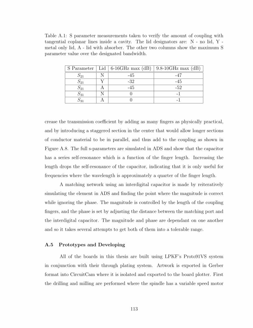
Table A.1: S parameter measurements taken to verify the amount of coupling withtangential coplanar lines inside a cavity. The lid designators are: N - no lid, Y -metal only lid, A - lid with absorber. The other two columns show the maximum Sparameter value over the designated bandwidth.
S Parameter Lid 6-16GHz max (dB) 9.8-10GHz max (dB)
S21 N -45 -47S21 Y -32 -45S21 A -45 -52S31 N 0 -1S31 A 0 -1
crease the transmission coefficient by adding as many fingers as physically practical,
and by introducing a staggered section in the center that would allow longer sections
of conductor material to be in parallel, and thus add to the coupling as shown in
Figure A.8. The full s-parameters are simulated in ADS and show that the capacitor
has a series self-resonance which is a function of the finger length. Increasing the
length drops the self-resonance of the capacitor, indicating that it is only useful for
frequencies where the wavelength is approximately a quarter of the finger length.
A matching network using an interdigital capacitor is made by reiteratively
simulating the element in ADS and finding the point where the magnitude is correct
while ignoring the phase. The magnitude is controlled by the length of the coupling
fingers, and the phase is set by adjusting the distance between the matching port and
the interdigital capacitor. The magnitude and phase are dependant on one another
and so it takes several attempts to get both of them into a tolerable range.
A.5 Prototypes and Developing
All of the boards in this thesis are built using LPKF’s Proto91VS system
in conjunction with their through plating system. Artwork is exported in Gerber
format into CircuitCam where it is isolated and exported to the board plotter. First
the drilling and milling are performed where the spindle has a variable speed motor
113
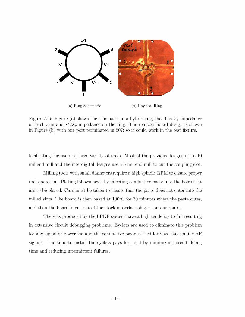
(a) Ring Schematic (b) Physical Ring
Figure A.6: Figure (a) shows the schematic to a hybrid ring that has Zo impedanceon each arm and
√2Zo impedance on the ring. The realized board design is shown
in Figure (b) with one port terminated in 50Ω so it could work in the test fixture.
facilitating the use of a large variety of tools. Most of the previous designs use a 10
mil end mill and the interdigital designs use a 5 mil end mill to cut the coupling slot.
Milling tools with small diameters require a high spindle RPM to ensure proper
tool operation. Plating follows next, by injecting conductive paste into the holes that
are to be plated. Care must be taken to ensure that the paste does not enter into the
milled slots. The board is then baked at 100oC for 30 minutes where the paste cures,
and then the board is cut out of the stock material using a contour router.
The vias produced by the LPKF system have a high tendency to fail resulting
in extensive circuit debugging problems. Eyelets are used to eliminate this problem
for any signal or power via and the conductive paste is used for vias that confine RF
signals. The time to install the eyelets pays for itself by minimizing circuit debug
time and reducing intermittent failures.
114
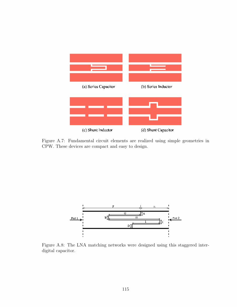
!"#$&%'
)(*%)#*"'#$% $&*()%*#)+,!
Figure A.7: Fundamental circuit elements are realized using simple geometries inCPW. These devices are compact and easy to design.
-. /
0
123 4
5678 9!: 678 9<;
Figure A.8: The LNA matching networks were designed using this staggered inter-digital capacitor.
115

116
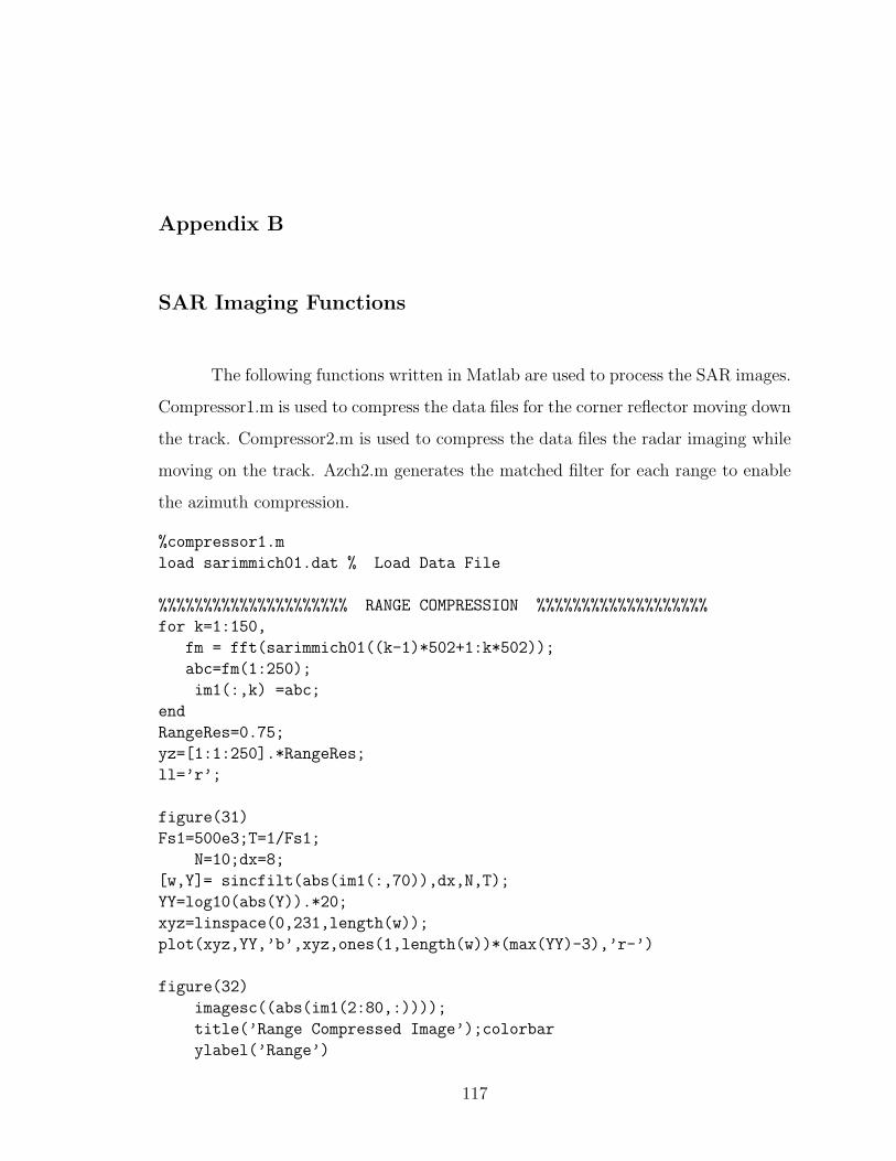
Appendix B
SAR Imaging Functions
The following functions written in Matlab are used to process the SAR images.
Compressor1.m is used to compress the data files for the corner reflector moving down
the track. Compressor2.m is used to compress the data files the radar imaging while
moving on the track. Azch2.m generates the matched filter for each range to enable
the azimuth compression.
%compressor1.m
load sarimmich01.dat % Load Data File
%%%%%%%%%%%%%%%%%%%%% RANGE COMPRESSION %%%%%%%%%%%%%%%%%%%
for k=1:150,
fm = fft(sarimmich01((k-1)*502+1:k*502));
abc=fm(1:250);
im1(:,k) =abc;
end
RangeRes=0.75;
yz=[1:1:250].*RangeRes;
ll=’r’;
figure(31)
Fs1=500e3;T=1/Fs1;
N=10;dx=8;
[w,Y]= sincfilt(abs(im1(:,70)),dx,N,T);
YY=log10(abs(Y)).*20;
xyz=linspace(0,231,length(w));
plot(xyz,YY,’b’,xyz,ones(1,length(w))*(max(YY)-3),’r-’)
figure(32)
imagesc((abs(im1(2:80,:))));
title(’Range Compressed Image’);colorbar
ylabel(’Range’)
117
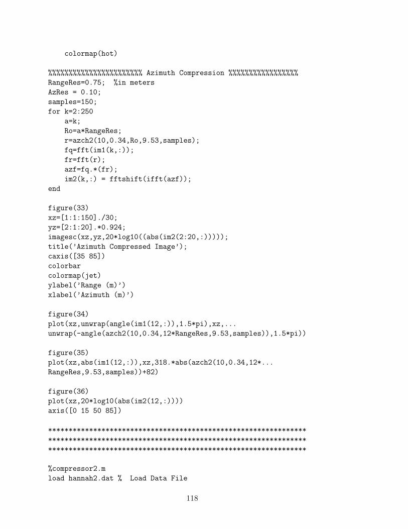
colormap(hot)
%%%%%%%%%%%%%%%%%%%%%%% Azimuth Compression %%%%%%%%%%%%%%%%%
RangeRes=0.75; %in meters
AzRes = 0.10;
samples=150;
for k=2:250
a=k;
Ro=a*RangeRes;
r=azch2(10,0.34,Ro,9.53,samples);
fq=fft(im1(k,:));
fr=fft(r);
azf=fq.*(fr);
im2(k,:) = fftshift(ifft(azf));
end
figure(33)
xz=[1:1:150]./30;
yz=[2:1:20].*0.924;
imagesc(xz,yz,20*log10((abs(im2(2:20,:)))));
title(’Azimuth Compressed Image’);
caxis([35 85])
colorbar
colormap(jet)
ylabel(’Range (m)’)
xlabel(’Azimuth (m)’)
figure(34)
plot(xz,unwrap(angle(im1(12,:)),1.5*pi),xz,...
unwrap(-angle(azch2(10,0.34,12*RangeRes,9.53,samples)),1.5*pi))
figure(35)
plot(xz,abs(im1(12,:)),xz,318.*abs(azch2(10,0.34,12*...
RangeRes,9.53,samples))+82)
figure(36)
plot(xz,20*log10(abs(im2(12,:))))
axis([0 15 50 85])
***************************************************************
***************************************************************
***************************************************************
%compressor2.m
load hannah2.dat % Load Data File
118
azsamp = 372;
% RANGE COMPRESSION
for k=1:azsamp,
fm = fft(hannah2((k-1)*250+1:k*250));
abc=fm(1:250);
im1(:,k) =abc;
end figure(31)
plot(20*log10(abs(im1)));
title(’Absolute Value of each Range Line’)
figure(32)
imagesc((abs(im1(2:80,:))));
title(’Range Compressed Image’);colorbar
ylabel(’Range in Samples, .75 meters per sample’)
colormap(jet)
% Azimuth Compression
RangeRes=0.75; %in meters
AzRes = 0.10; samples=azsamp; for k=5:250
a=k;
Ro=a*RangeRes;
r=azch2(10,0.34,Ro,5,samples);
fq=fft(im1(k,:));
fr=fft(r);
azf=fq.*(fr);
im2(k,:) = fftshift(ifft(azf));
end
figure(33) xz=[1:1:372].*AzRes; yz=[5:1:200].*RangeRes;
surf(xz,yz,(abs(im2(5:200,:))).^0.1), shading interp
title(’Azimuth Compressed Image’);
caxis([1.0 1.9]) colormap(gray)
view(0,90) ylabel(’Range (m)’) xlabel(’Azimuth (m)’)
axis equal
axis([0 37 5 65])
figure(34)
plot(xz,unwrap(angle(im1(22,:)),1.5*pi),xz,...
unwrap(angle(azch2(10,0.34,22*RangeRes,9.53,samples)),1.5*pi))
figure(35)
plot(xz,abs(im1(22,:)),xz,100.*abs(azch2(10,0.34,22*...
RangeRes,9.53,samples)))
figure(36) plot(xz,20*log10(abs(im2(22,:))))
119
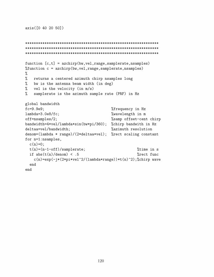
axis([0 40 20 50])
**************************************************************
**************************************************************
**************************************************************
function [c,t] = azchirp(bw,vel,range,samplerate,nsamples)
%function c = azchirp(bw,vel,range,samplerate,nsamples)
%
% returns a centered azimuth chirp nsamples long
% bw is the antenna beam width (in deg)
% vel is the velocity (in m/s)
% samplerate is the azimuth sample rate (PRF) in Hz
global bandwidth
fc=9.9e9; %frequency in Hz
lambda=3.0e8/fc; %wavelength in m
off=nsamples/2; %samp offset-cent chirp
bandwidth=4*vel/lambda*sin(bw*pi/360); %chirp bandwith in Hz
deltaa=vel/bandwidth; %azimuth resolution
denom=(lambda * range)/(2*deltaa*vel); %rect scaling constant
for n=1:nsamples,
c(n)=0;
t(n)=(n-1-off)/samplerate; %time in s
if abs(t(n)/denom) < .5 %rect func
c(n)=exp(-j*(2*pi*vel^2/(lambda*range))*t(n)^2);%chirp wave
end
end
120

Appendix C
SAR Visual Basic Code for Instrument Control
Option Explicit
Dim flag1 As Integer, flag2 As Integer, pcdacval As Long
Dim counts As Long, trans As Single, flagendcal As Integer
Dim flagcalmes As Boolean, freqcap As String, runflag As Integer
Dim flagrun2 As Integer
’End of Globals
Private Sub channa_sld_change()
phcomm1.Output = "w" + Format(channa_sld.Value, "000")
Text13.Text = channa_sld.Value
End Sub
Private Sub channb_sld_Click()
phcomm1.Output = "x" + Format(channb_sld.Value, "000")
Text14.Text = channb_sld.Value
End Sub
Public Sub Form_Load()
phcomm1.EOFEnable = True
If phcomm1.PortOpen = False Then
phcomm1.PortOpen = True
End If
Text7.Text = "Open"
’Text4.Text = "11111900" ’Intial Count
Text5.Text = "3" ’Tolerance
Text8.Text = "100" ’DAC Increment
Text9.Text = "200" ’Bandwidth
Text10.Text = "9800" ’Intial Frequency
trans = 0.00088215 * 8 ’count to MHz coefficient
calcomm.Text = " i DAC delta Frequency" + Chr(10)
End Sub
Private Sub cleartxt_but_Click()
121
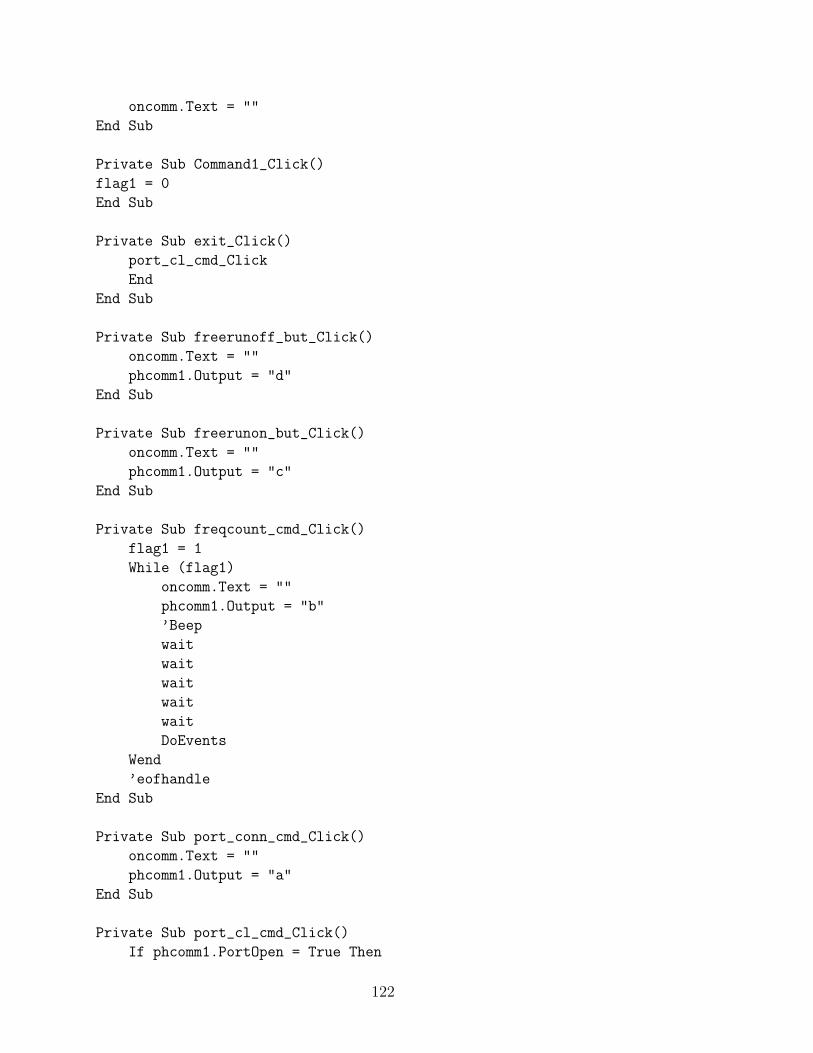
oncomm.Text = ""
End Sub
Private Sub Command1_Click()
flag1 = 0
End Sub
Private Sub exit_Click()
port_cl_cmd_Click
End
End Sub
Private Sub freerunoff_but_Click()
oncomm.Text = ""
phcomm1.Output = "d"
End Sub
Private Sub freerunon_but_Click()
oncomm.Text = ""
phcomm1.Output = "c"
End Sub
Private Sub freqcount_cmd_Click()
flag1 = 1
While (flag1)
oncomm.Text = ""
phcomm1.Output = "b"
’Beep
wait
wait
wait
wait
wait
DoEvents
Wend
’eofhandle
End Sub
Private Sub port_conn_cmd_Click()
oncomm.Text = ""
phcomm1.Output = "a"
End Sub
Private Sub port_cl_cmd_Click()
If phcomm1.PortOpen = True Then
122

phcomm1.PortOpen = False
End If
Text7.Text = "Closed"
End Sub
Private Sub port_op_cmd_Click()
If phcomm1.PortOpen = False Then
phcomm1.PortOpen = True
End If
Text7.Text = "Open"
End Sub
Private Sub port_opt_Click(Index As Integer)
port_cl_cmd_Click
phcomm1.CommPort = Index + 1
End Sub
Private Sub phcomm1_OnComm()
Dim temp
temp = phcomm1.CommEvent
Text1.Text = Text1.Text + Str(temp)
Select Case phcomm1.CommEvent
’ Handle each event or error by placing
’ code below each case statement
’ Errors
Case comEventBreak ’ A Break was received.
MsgBox ("Break in Comm data")
Case comEventFrame ’ Framing Error
Case comEventOverrun ’ Data Lost.
Case comEventRxOver ’ Receive buffer overflow.
Case comEventRxParity ’ Parity Error.
Case comEventTxFull ’ Transmit buffer full.
Case comEventDCB ’ Unexpected error retrieving DCB]
’ Events
Case comEvCD ’ Change in the CD line.
Case comEvCTS ’ Change in the CTS line.
Case comEvDSR ’ Change in the DSR line.
Case comEvRing ’ Change in the Ring Indicator.
Case comEvReceive ’ Received RThreshold # of
’ chars.
Case comEvSend ’ There are SThreshold number of
wait ’ characters in the transmit
eofhandle ’ buffer.
123
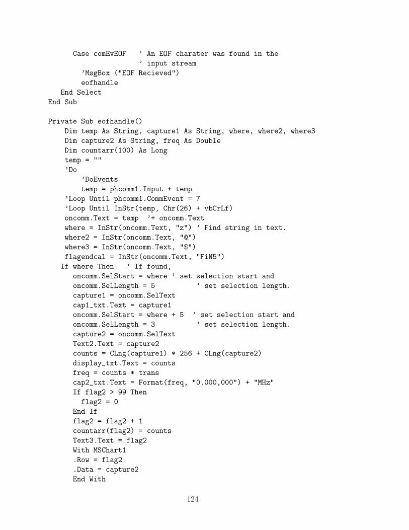
Case comEvEOF ’ An EOF charater was found in the
’ input stream
’MsgBox ("EOF Recieved")
eofhandle
End Select
End Sub
Private Sub eofhandle()
Dim temp As String, capture1 As String, where, where2, where3
Dim capture2 As String, freq As Double
Dim countarr(100) As Long
temp = ""
’Do
’DoEvents
temp = phcomm1.Input + temp
’Loop Until phcomm1.CommEvent = 7
’Loop Until InStr(temp, Chr(26) + vbCrLf)
oncomm.Text = temp ’+ oncomm.Text
where = InStr(oncomm.Text, "z") ’ Find string in text.
where2 = InStr(oncomm.Text, "@")
where3 = InStr(oncomm.Text, "$")
flagendcal = InStr(oncomm.Text, "FiN5")
If where Then ’ If found,
oncomm.SelStart = where ’ set selection start and
oncomm.SelLength = 5 ’ set selection length.
capture1 = oncomm.SelText
cap1_txt.Text = capture1
oncomm.SelStart = where + 5 ’ set selection start and
oncomm.SelLength = 3 ’ set selection length.
capture2 = oncomm.SelText
Text2.Text = capture2
counts = CLng(capture1) * 256 + CLng(capture2)
display_txt.Text = counts
freq = counts * trans
cap2_txt.Text = Format(freq, "0.000,000") + "MHz"
If flag2 > 99 Then
flag2 = 0
End If
flag2 = flag2 + 1
countarr(flag2) = counts
Text3.Text = flag2
With MSChart1
.Row = flag2
.Data = capture2
End With
124

flagrun2 = 0
End If
If where2 Then ’ If found,
oncomm.SelStart = where2 ’ set selection start and
oncomm.SelLength = 15 ’ set selection length.
calcomm.Text = calcomm.Text + oncomm.SelText + ", " +_
freqcap + Chr(10)
flagcalmes = False
End If
If where3 Then ’ If found,
oncomm.SelStart = where3 ’ set selection start and
oncomm.SelLength = 5 ’ set selection length.
capture1 = oncomm.SelText
cap1_txt.Text = capture1
oncomm.SelStart = where3 + 5 ’ set selection start and
oncomm.SelLength = 3 ’ set selection length.
capture2 = oncomm.SelText
Text2.Text = capture2
counts = CLng(capture1) * 256 + CLng(capture2)
display_txt.Text = counts
freq = counts * trans
cap2_txt.Text = Format(freq, "0.000,000") + "MHz"
flagrun2 = 0
End If
End Sub
Private Sub wait()
Dim i
For i = 1 To 200000
Next
End Sub
Private Sub reset_Click()
Form_Load
End Sub
Private Sub Slider1_Change()
dacval_txt.Text = Slider1.Value
phcomm1.Output = "e" + Format(Slider1.Value, "00000")
wait
wait
wait
DoEvents
phcomm1.Output = "b"
End Sub
125
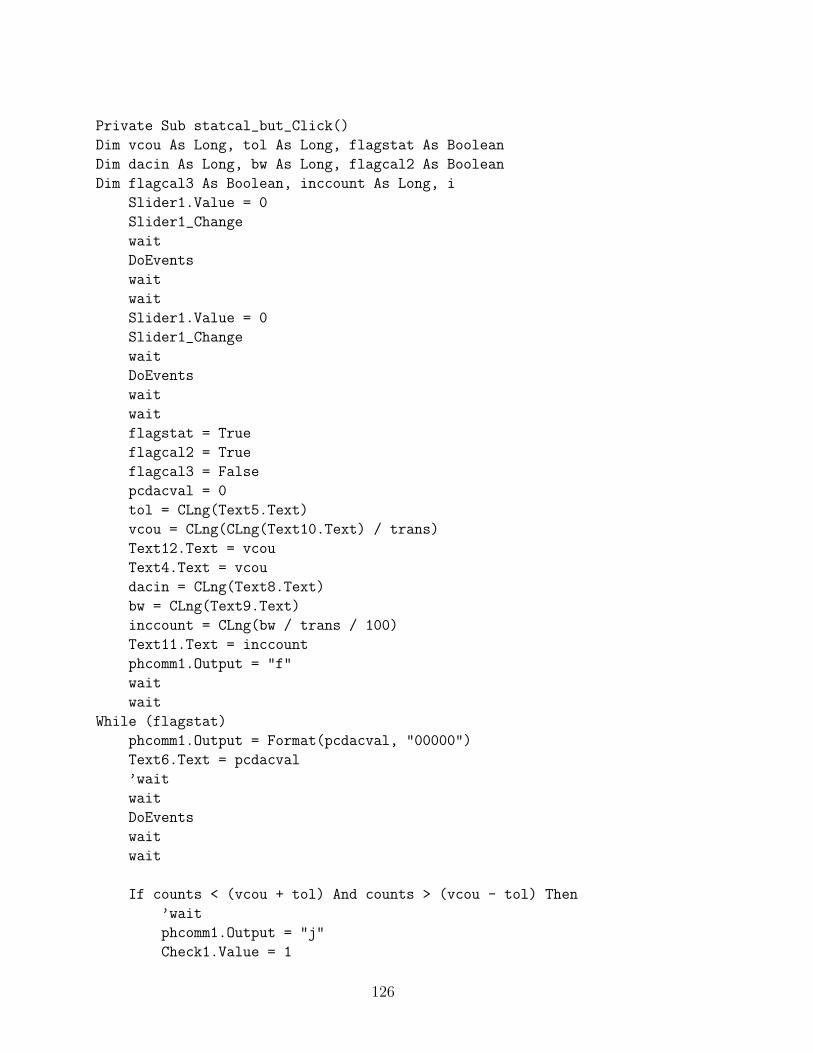
Private Sub statcal_but_Click()
Dim vcou As Long, tol As Long, flagstat As Boolean
Dim dacin As Long, bw As Long, flagcal2 As Boolean
Dim flagcal3 As Boolean, inccount As Long, i
Slider1.Value = 0
Slider1_Change
wait
DoEvents
wait
wait
Slider1.Value = 0
Slider1_Change
wait
DoEvents
wait
wait
flagstat = True
flagcal2 = True
flagcal3 = False
pcdacval = 0
tol = CLng(Text5.Text)
vcou = CLng(CLng(Text10.Text) / trans)
Text12.Text = vcou
Text4.Text = vcou
dacin = CLng(Text8.Text)
bw = CLng(Text9.Text)
inccount = CLng(bw / trans / 100)
Text11.Text = inccount
phcomm1.Output = "f"
wait
wait
While (flagstat)
phcomm1.Output = Format(pcdacval, "00000")
Text6.Text = pcdacval
’wait
wait
DoEvents
wait
wait
If counts < (vcou + tol) And counts > (vcou - tol) Then
’wait
phcomm1.Output = "j"
Check1.Value = 1
126
freqcap = cap2_txt.Text
calcomm.Text = calcomm.Text + " 1st, " +_
Format(pcdacval, "00000") + _
", 000, " + freqcap + Chr(10)
flagstat = False
ElseIf counts > vcou Then
If flagcal2 Then
dacin = 10
flagcal3 = True
End If
Text8.Text = dacin
pcdacval = pcdacval - dacin
phcomm1.Output = "i"
Else
pcdacval = pcdacval + dacin
phcomm1.Output = "i"
If flagcal3 Then
dacin = 1
flagcal2 = False
End If
End If
Wend
’wait
wait
For i = 1 To 100
Beep
Next
’vcou = vcou - inccount
’DoEvents
While Not flagendcal
vcou = vcou + inccount
flagcalmes = True
Text12.Text = vcou
While flagcalmes
If counts < (vcou + tol) And counts > (vcou - tol) Then
’wait
freqcap = cap2_txt.Text
phcomm1.Output = "k"
ElseIf counts > vcou Then
’wait
phcomm1.Output = "l"
Else
’wait
phcomm1.Output = "m"
End If
127
wait
DoEvents
’wait
’wait
’DoEvents
Wend
Wend
For i = 1 To 1000
Beep
Next
End Sub
Private Sub tranon_but_Click()
phcomm1.Output = "g"
End Sub
Private Sub tranoff_but_Click()
runflag = 0
End Sub
128
Appendix D
PicBasicPro Code for Transmitter Module
’10 GHz SAR Using FM/CW
’Written by Ryan Smith
’Date 8/12/00
’Code generated for a PIC16C73A
’-----------------------------------------------------------
’Variable Definitions
’Interrupt Variables
wsave var byte $20 system ’saved in such a manner to protect
wsave1 var byte $a0 system ’both banks of registers
ssave var byte $21 system
psave var byte $22 system
fsave var byte $23 system
’counter con 125
baud con 84 ’Baud Rate (9600)
c var byte ’character
spout var PortC.6 ’Serial Output Port
spin var PortC.7 ’Serial Input Port
trigger var PortC.4 ’trigger & EXT Counter:Reset
s1 var PortC.2 ’SR:0-shifts right 1-parallel load
exttime var PortC.1 ’Line to turn ext. counter on(1) or off(0)
srclk var PortC.5 ’load dac & shift register clock
datpin var PortC.3 ’shifted in data
fin var PortC.0 ’Inut frequency to internal timer
datain var byte
Fcap var word bank1 ’Captured frequency forced to filebank 1
Fcaph var Fcap.byte1 ’high byte of Fcap
Fcapl var Fcap.byte0 ’low byte of Fcap
129
dacval var word ’digital value to send to dac
dacvalh var dacval.byte1 ’high byte of dacval
dacvall var dacval.byte0 ’low byte of dacval
deltavl var byte[51] ’incremental voltage array upper
deltavu var byte[51] ’incremental voltage array upper
pcdacval var word ’digital DAC value received from PC
i var word ’loop counter
j var word ’loop counter
k var byte ’loop counter
flag1 var bit ’run loop flag
’-----------------------------------------------------------
’Initialization
’---------------------------------------------------
’Timer1 set up in Capture Mode
T1CON = %000110 ’Timer1 setup
’---------------------------------------------------
’Set up ports...
define OSC 20
TRISA = %00000000 ’0 is output
TRISB = %00000000 ’1 is input
TRISC = %10001001
ADCON1 = %111
’---------------------------------------------------
’Initial States
srclk=0:exttime=1:trigger=0
for i = 0 to 49
deltaVL[i]=160
deltaVU[i]=160
next i
’deltaVL[0] = 0
serout2 spout,baud,["10 GHZ SAR Transmitter",169,10,_
"Microwave Earth Remote Sensing",10,_
"Brigham Young University",10,"8/12/00"_
,13,10,26,13,10,13,10,26,13,10]
while 1
cmdln:
serin2 spin,baud,[c]
if c="a" then
serout2 spout,baud,["Communication Established",_
13,10,26,13,10]
endif
if c="b" then
130
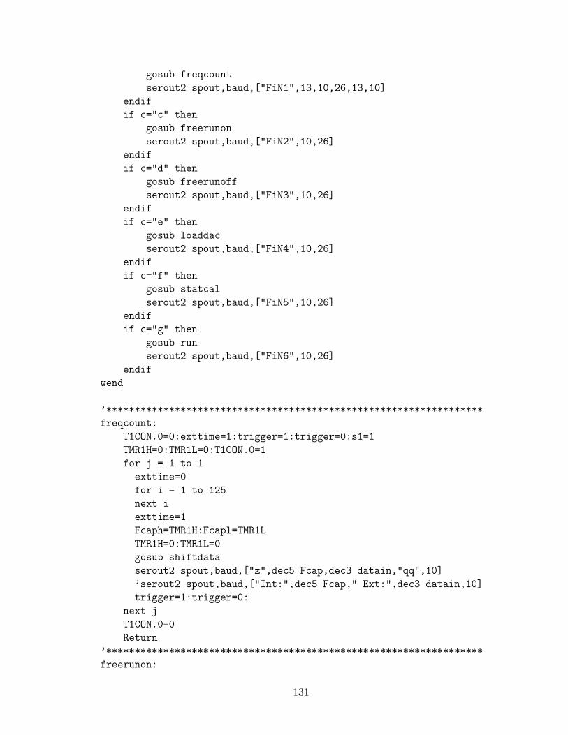
gosub freqcount
serout2 spout,baud,["FiN1",13,10,26,13,10]
endif
if c="c" then
gosub freerunon
serout2 spout,baud,["FiN2",10,26]
endif
if c="d" then
gosub freerunoff
serout2 spout,baud,["FiN3",10,26]
endif
if c="e" then
gosub loaddac
serout2 spout,baud,["FiN4",10,26]
endif
if c="f" then
gosub statcal
serout2 spout,baud,["FiN5",10,26]
endif
if c="g" then
gosub run
serout2 spout,baud,["FiN6",10,26]
endif
wend
’******************************************************************
freqcount:
T1CON.0=0:exttime=1:trigger=1:trigger=0:s1=1
TMR1H=0:TMR1L=0:T1CON.0=1
for j = 1 to 1
exttime=0
for i = 1 to 125
next i
exttime=1
Fcaph=TMR1H:Fcapl=TMR1L
TMR1H=0:TMR1L=0
gosub shiftdata
serout2 spout,baud,["z",dec5 Fcap,dec3 datain,"qq",10]
’serout2 spout,baud,["Int:",dec5 Fcap," Ext:",dec3 datain,10]
trigger=1:trigger=0:
next j
T1CON.0=0
Return
’******************************************************************
freerunon:
131
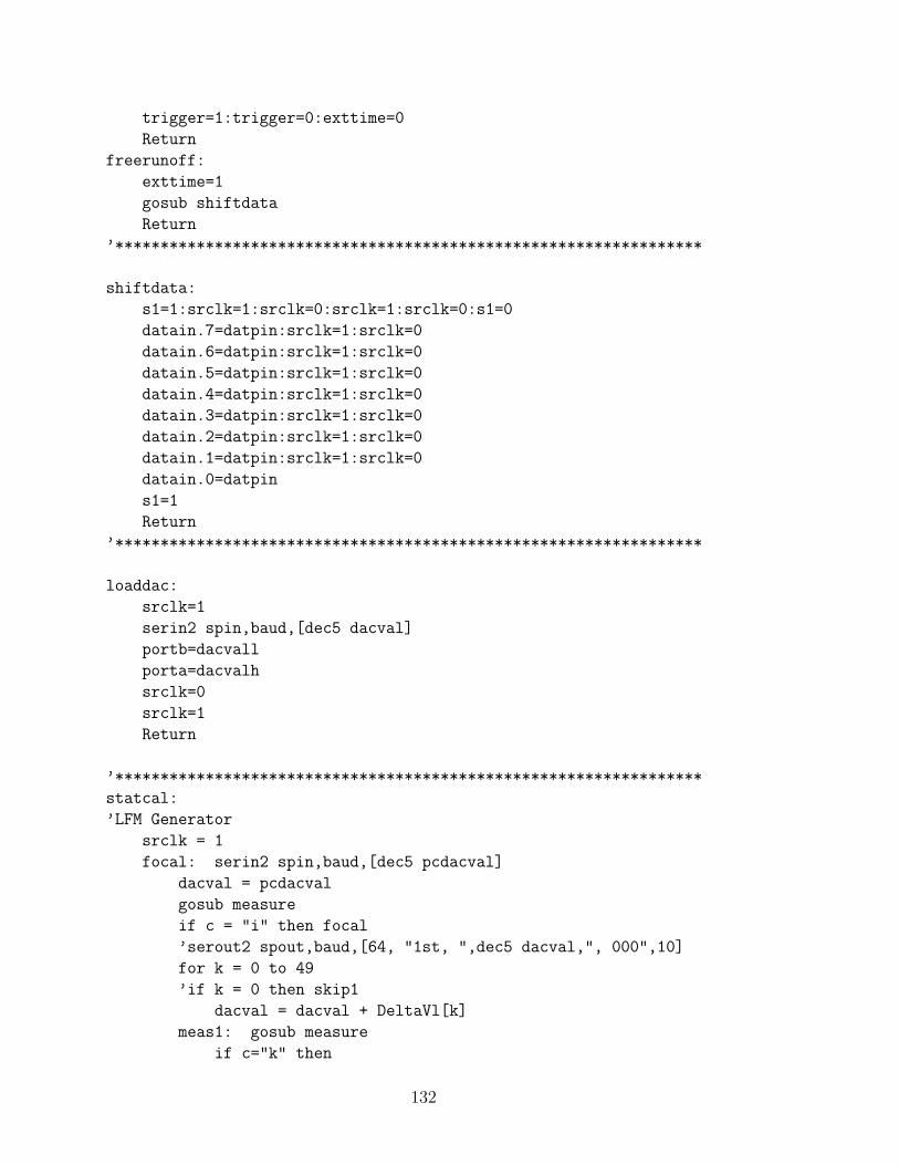
trigger=1:trigger=0:exttime=0
Return
freerunoff:
exttime=1
gosub shiftdata
Return
’*****************************************************************
shiftdata:
s1=1:srclk=1:srclk=0:srclk=1:srclk=0:s1=0
datain.7=datpin:srclk=1:srclk=0
datain.6=datpin:srclk=1:srclk=0
datain.5=datpin:srclk=1:srclk=0
datain.4=datpin:srclk=1:srclk=0
datain.3=datpin:srclk=1:srclk=0
datain.2=datpin:srclk=1:srclk=0
datain.1=datpin:srclk=1:srclk=0
datain.0=datpin
s1=1
Return
’*****************************************************************
loaddac:
srclk=1
serin2 spin,baud,[dec5 dacval]
portb=dacvall
porta=dacvalh
srclk=0
srclk=1
Return
’*****************************************************************
statcal:
’LFM Generator
srclk = 1
focal: serin2 spin,baud,[dec5 pcdacval]
dacval = pcdacval
gosub measure
if c = "i" then focal
’serout2 spout,baud,[64, "1st, ",dec5 dacval,", 000",10]
for k = 0 to 49
’if k = 0 then skip1
dacval = dacval + DeltaVl[k]
meas1: gosub measure
if c="k" then
132
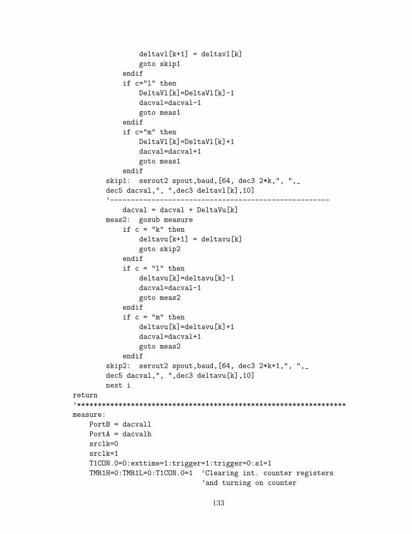
deltavl[k+1] = deltavl[k]
goto skip1
endif
if c="l" then
DeltaVl[k]=DeltaVl[k]-1
dacval=dacval-1
goto meas1
endif
if c="m" then
DeltaVl[k]=DeltaVl[k]+1
dacval=dacval+1
goto meas1
endif
skip1: serout2 spout,baud,[64, dec3 2*k,", ",_
dec5 dacval,", ",dec3 deltavl[k],10]
’-----------------------------------------------------
dacval = dacval + DeltaVu[k]
meas2: gosub measure
if c = "k" then
deltavu[k+1] = deltavu[k]
goto skip2
endif
if c = "l" then
deltavu[k]=deltavu[k]-1
dacval=dacval-1
goto meas2
endif
if c = "m" then
deltavu[k]=deltavu[k]+1
dacval=dacval+1
goto meas2
endif
skip2: serout2 spout,baud,[64, dec3 2*k+1,", ",_
dec5 dacval,", ",dec3 deltavu[k],10]
next i
return
’*****************************************************************
measure:
PortB = dacvall
PortA = dacvalh
srclk=0
srclk=1
T1CON.0=0:exttime=1:trigger=1:trigger=0:s1=1
TMR1H=0:TMR1L=0:T1CON.0=1 ’Clearing int. counter registers
’and turning on counter
133
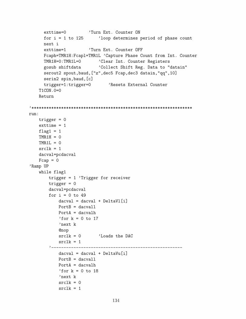
exttime=0 ’Turn Ext. Counter ON
for i = 1 to 125 ’loop determines period of phase count
next i
exttime=1 ’Turn Ext. Counter OFF
Fcaph=TMR1H:Fcapl=TMR1L ’Capture Phase Count from Int. Counter
TMR1H=0:TMR1L=0 ’Clear Int. Counter Registers
gosub shiftdata ’Collect Shift Reg. Data to "datain"
serout2 spout,baud,["z",dec5 Fcap,dec3 datain,"qq",10]
serin2 spin,baud,[c]
trigger=1:trigger=0 ’Resets External Counter
T1CON.0=0
Return
’*****************************************************************
run:
trigger = 0
exttime = 1
flag1 = 1
TMR1H = 0
TMR1L = 0
srclk = 1
dacval=pcdacval
Fcap = 0
’Ramp UP
while flag1
trigger = 1 ’Trigger for receiver
trigger = 0
dacval=pcdacval
for i = 0 to 49
dacval = dacval + DeltaVl[i]
PortB = dacvall
PortA = dacvalh
’for k = 0 to 17
’next k
@nop
srclk = 0 ’Loads the DAC
srclk = 1
’-----------------------------------------------------
dacval = dacval + DeltaVu[i]
PortB = dacvall
PortA = dacvalh
’for k = 0 to 18
’next k
srclk = 0
srclk = 1
134
next i
’---------------------------------------------------------
’Ramp Down
dacval=pcdacval
PortB = dacvall
PortA = dacvalh
srclk = 0
srclk = 1
pause 10
T1CON.0=0:s1=1
TMR1H=0:TMR1L=0:T1CON.0=1 ’Clearing int. counter
’registers and turning on counter
exttime=0 ’Turn Ext. Counter ON
for i = 1 to 125 ’loop determines period of phase count
next i
exttime=1 ’Turn Ext. Counter OFF
Fcaph=TMR1H:Fcapl=TMR1L ’Capture Phase Count from
’Int. Counter
TMR1H=0:TMR1L=0 ’Clear Int. Counter Registers
gosub shiftdata ’Collect Shift Reg. Data to "datain"
serout2 spout,baud,["$",dec5 Fcap,dec3 datain,"qq",10]
0serin2 spin,baud,[dec5 pcdacval, dec1 flag1]
T1CON.0=0
wend
serout2 spout,baud,["FiN2",10]
return
’*****************************************************************
’VCO Ramp
ramp:
dacval = 0
’Ramp UP
PortB = dacvall
PortA = dacvalh
srclk=0
srclk=1
pause 10
for j = 0 to 100
for i = 0 to 2046
dacval = dacval + 8
PortB = dacvall
PortA = dacvalh
srclk=0
srclk=1
135

next i
’---------------------------------------------------------
for i = 0 to 2046
dacval = dacval - 8
PortB = dacvall
PortA = dacvalh
srclk=0
srclk=1
next i
next j
serout2 spout,baud,["FiN6",10]
return
’*****************************************************************
136

Appendix E
PicBasicPro Code for Receiver Module
’10 GHz SAR Reciever
’Written by Ryan Smith
’Date 8/24/00
’Code generated for a PIC16C73A
baud con 84 ’Baud Rate (9600)
c var byte ’character
spout var PortC.6 ’Serial Output Port
spin var PortC.7 ’Serial Input Port
Asdata var PortA.0 ’Channel A Serial Data Line
ACLK var PortA.1
ADaten var PortA.2
AbPO var PortA.3
gaina var byte
gainb var byte
Bsdata var PortB.7 ’Channel A Serial Data Line
BCLK var PortB.6
BDaten var PortB.5
BbPO var PortB.4
’Set up ports...
define OSC 20
TRISA = %00000000 ’0 is output
TRISB = %00000000 ’1 is input
TRISC = %10001001
ADCON1 = %111
137
AbPO = 1: ADaten = 1: ACLK = 0
BbPO = 1: BDaten = 1: BCLK =0
serout2 spout,baud,["10 GHZ SAR Receiver",169,10,_
"Microwave Earth Remote Sensing",10,_
"Brigham Young University",10,"8/12/00",13,10,_
26,13,10,13,10,26,13,10]
while 1
cmdln:
serin2 spin,baud,[c]
if c="a" then
serout2 spout,baud,["Communication Established",_
13,10,26,13,10]
endif
if c="w" then
gosub channa
serout2 spout,baud,["FiN8",10,26]
endif
if c="x" then
gosub channb
serout2 spout,baud,["FiN9",10,26]
endif
wend
’*********************************************************
channa:
serin2 spin,baud,[dec3 gaina]
ADaten = 0
Asdata = gaina.7:ACLK=1:ACLK=0
Asdata = gaina.6:ACLK=1:ACLK=0
Asdata = gaina.5:ACLK=1:ACLK=0
Asdata = gaina.4:ACLK=1:ACLK=0
Asdata = gaina.3:ACLK=1:ACLK=0
Asdata = gaina.2:ACLK=1:ACLK=0
Asdata = gaina.1:ACLK=1:ACLK=0
Asdata = gaina.0:ACLK=1:ACLK=0
ADaten = 1
Return
’**********************************************************
channb:
serin2 spin,baud,[dec3 gainb]
BDaten = 0
Bsdata = gainb.7:BCLK=1:BCLK=0
Bsdata = gainb.6:BCLK=1:BCLK=0
138

Bsdata = gainb.5:BCLK=1:BCLK=0
Bsdata = gainb.4:BCLK=1:BCLK=0
Bsdata = gainb.3:BCLK=1:BCLK=0
Bsdata = gainb.2:BCLK=1:BCLK=0
Bsdata = gainb.1:BCLK=1:BCLK=0
Bsdata = gainb.0:BCLK=1:BCLK=0
BDaten = 1
Return
139

140

Appendix F
PECL Design Overview
F.1 ECL Basic Gate
Emitter Coupled Logic (ECL) in Pico Seconds (ECLinPS) logic family is the
focus of this overview. Data sheets often confuse the issue of ECL design by many
equations and charts to help designers with transmission line effects due to the high
speed of ECL devices. It is much simpler to have a basic understanding of an ECL de-
vice layout and its DC and AC electrical characteristics, and then apply transmission
theory to match the transmission lines.
F.2 Positive Emitter Coupled Logic
ECL is developed using ground for VCC and −5V for VEE. This voltage ar-
rangement is selected because ground is a relatively stable power plane, and the
performance of ECL devices are sensitive to fluctuations in VCC voltage but are tol-
erant of noise in the VEE power plane. Positive ECL (PECL) is the name given when
an ECL circuit is designed using a +5V supply for VCC and ground for VEE. Any
ECL chip will work in a PECL design with the exception of logic translators to and
from TTL. Specific translators are available for both PECL and ECL circuits. PECL
can be implemented by the careful design of a power plane for VCC and VTT which
should be well isolated from analog and digital planes. Table F.1 shows specified
voltage levels by Motorola [43] for a temperature range of 0 to 85C.
It is seen from the conversion table that the voltage is simply shifted up by 5
Volts. It is also seen from specifications that the typical AC signal is approximately
800 mVpp. This is equivalent to 2.0 dBm referenced to a 50 Ω system.
141
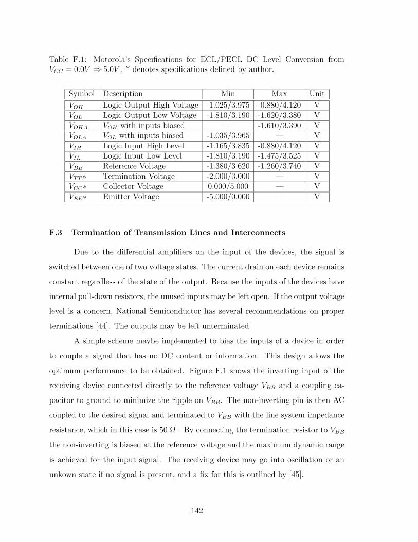
Table F.1: Motorola’s Specifications for ECL/PECL DC Level Conversion fromVCC = 0.0V ⇒ 5.0V . * denotes specifications defined by author.
Symbol Description Min Max Unit
VOH Logic Output High Voltage -1.025/3.975 -0.880/4.120 VVOL Logic Output Low Voltage -1.810/3.190 -1.620/3.380 VVOHA VOH with inputs biased — -1.610/3.390 VVOLA VOL with inputs biased -1.035/3.965 — VVIH Logic Input High Level -1.165/3.835 -0.880/4.120 VVIL Logic Input Low Level -1.810/3.190 -1.475/3.525 VVBB Reference Voltage -1.380/3.620 -1.260/3.740 VVTT∗ Termination Voltage -2.000/3.000 — VVCC∗ Collector Voltage 0.000/5.000 — VVEE∗ Emitter Voltage -5.000/0.000 — V
F.3 Termination of Transmission Lines and Interconnects
Due to the differential amplifiers on the input of the devices, the signal is
switched between one of two voltage states. The current drain on each device remains
constant regardless of the state of the output. Because the inputs of the devices have
internal pull-down resistors, the unused inputs may be left open. If the output voltage
level is a concern, National Semiconductor has several recommendations on proper
terminations [44]. The outputs may be left unterminated.
A simple scheme maybe implemented to bias the inputs of a device in order
to couple a signal that has no DC content or information. This design allows the
optimum performance to be obtained. Figure F.1 shows the inverting input of the
receiving device connected directly to the reference voltage VBB and a coupling ca-
pacitor to ground to minimize the ripple on VBB. The non-inverting pin is then AC
coupled to the desired signal and terminated to VBB with the line system impedance
resistance, which in this case is 50 Ω . By connecting the termination resistor to VBB
the non-inverting is biased at the reference voltage and the maximum dynamic range
is achieved for the input signal. The receiving device may go into oscillation or an
unkown state if no signal is present, and a fix for this is outlined by [45].
142
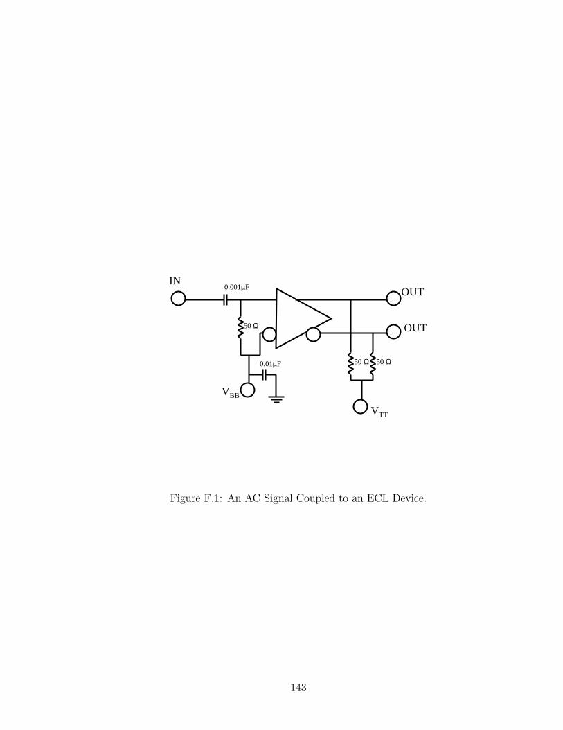
50 Ω50 Ω
50 Ω
IN
VBB
VTT
0.01µF
0.001µF
OUT
OUT
Figure F.1: An AC Signal Coupled to an ECL Device.
143

144
Bibliography
[1] F. T. Ulaby, R. K. Moore, and A. K. Fung, Microwave Remote Sensing Active
and Passive, vol. I, Artech House, 1981.
[2] R. L. Smith, “Rain and cloud cover detection in south asia”, EcEn Department
Report TR-L000-01.1, Brigham Young University, 459 Clyde Building, Provo,
Utah, 84602, April 2001.
[3] A. E. Robertson, “Multi-baseline interferometric sar for iterative height esti-
mation”, Master’s thesis, Brigham Young University, Provo, Utah, December
1998.
[4] M. Zink and R. Bamler, “X-sar radiometric calibration and data quality”, IEEE
TRANSACTIONS ON Geoscience and Remote Sensing, vol. 33, no. 12, 1995.
[5] R. L. Jordan, B. L. Huneycutt, and M. Werner, “The sir-c/s-sar synthetic aper-
ture radar system”, IEEE TRANSACTIONS ON Geoscience and Remote Sens-
ing, vol. 33, no. 4, pp. 829–839, July 1995.
[6] Staff, “The critical role of sar in earth system science”, White paper, Alaska
SAR Facility User Working Group, June 1998.
[7] Y. Kim, Y. Lou, J. van Zyl, L. Maldonado, T. Miller, T. Sato, and W. Skot-
nicki, “Nasa/jpl airborne three-frequency polarimetric/interferometric sar sys-
tem”, IEEE Geoscience and Remote Sensing Symposium, vol. 3, pp. 1612–1614,
May 1996.
[8] G. F. Adams, D. A. Ausherman, S. L. Crippen, G. T. Sos, B. P. Williams, and
R. Heidelbach, “The erim interferometric sar: Ifsare”, IEEE Aerospace and
Electronics Systems Magazine, vol. 11, no. 12, pp. 31–35, December 1996.
145

[9] J. B. Mercer and M. Gill, “Radar-derived dems for urban areas”, ISPRS Com-
mission IV, vol. 3, September 1998.
[10] C. L. Glennie, An Analysis of Airborne Gravity by Strapdown INS/DGPS, PhD
thesis, University of Calgary, 2500 University Drive NW,Calgary, AB, T2N 1N4,
1999.
[11] B. Bullock and L. Fosse, “Accurate, low-cost digital elevation model (dem)
products”, Wall Street Coporate Reporter, vol. 6, no. 21, September 2001.
[12] B. R. Jarrett, “Byu sar, a low cost, compact synthetic aperture radar”, Master’s
thesis, Brigham Young University, Provo, Utah, August 1994.
[13] D. G. Thompson, D. V. Arnold, D. G. Long, G. F. Miner, M. A. Jensen, T. W.
Karlinsey, A. E. Robertson, and J. S. Bates, “Ysar and yinsar: Compact, low-
cost synthetic aperture radars”, in European Conference on Synthetic Aperture
Radar, Friedrichshafen, Germany, May 1998, pp. 25–27.
[14] D. G. Thompson, D. V. Arnold, D. G. Long, G. F. Miner, T. W. Karlinsey, and
A. E. Robertson, “Ysar: A compact, low-cost synthetic aperture radar”, in
IGARSS, Singapore, August 1997, IEEE, pp. 386–388.
[15] D. G. Thompson, Innovative Radar Interferometry, PhD thesis, Brigham Young
University, 459 Clyde Building, Provo, Utah, 84602, August 2001.
[16] D. G. Thompson, D. V. Arnold, and D. G. Long, “Yinsar: a compact, low-cost
interferometric sythetic aperture radar”, in IGARSS, Hamburg, Germany, July
1999, IEEE, pp. 598–600.
[17] R. B. Lundgreen, “Method of motion compensation of yinsar data”, Master’s
thesis, Brigham Young University, Provo, Utah, August 2001.
[18] M. Soumekh, “Wide-bandwidth continous-wave monostatic/bistatic synthetic
aperture radar imaging”, in 1998 International Conference on Image Processing.
IEEE, 1998, vol. 3, pp. 361–365.
146

[19] M. Soumekh, “Fm-cw sar and phased array spatial-velocity imaging”, in 1994
International Conference on Image Processing. IEEE, 1994, vol. 1, pp. 471–475.
[20] H. D. Griffiths, “Conceptual design of an ultra high-resolution mm-wave syn-
thetic aperture radar”, in Proceedings of the 1996 IEEE National Radar Con-
ference. IEEE, 1996, pp. 225–260.
[21] G. Connan, H. D. Griffiths, and P. V. Brennan, “Fmcw-sar development for
internal wave imaging”, in MTS/IEEE Conference Proceedings. IEEE, 1997,
vol. 1, pp. 73–78.
[22] S. Haykin, Adaptive Filter Theory, Prentice Hall, 2 edition, 1991.
[23] A. V. Oppenheim, Willsky, and Nawab, SIGNALS & SYSTEMS, Prentice Hall,
2 edition, 1997.
[24] H. R. Raemer, Radar Systems Principles, CRC Press, 1996.
[25] P. D. L. Beasely and A. G. Stove, “Pilot - an example of advanced fmcw tech-
niques”, IEEE Colloquium on High Time-Bandwidth Product Waveforms in
Radar and Sonar, pp. 10/1–10/5, 1991.
[26] J. C. Curlander and R. N. McDonough, Synthetic Aperture Radar: Systems and
Signal Processing, Remote Sensing. Wiley, 1991.
[27] D. V. Arnold, “Vector quantization of synthetic array radar data”, Master’s
thesis, Brigham Young University, Provo, Utah, 1987.
[28] F. T. Ulaby, R. K. Moore, and A. K. Fung, Microwave Remote Sensing Active
and Passive, vol. II, Artech House, 1986.
[29] S. S. Piper, “Homodyne fmcw radar range resolution effects with sinusodial
nonlinearities in the frequency sweep”, in Record of the IEEE 95 International
Radar Conference. IEEE, 1995, pp. 563–567.
147

[30] C. Weidong, X. Shanjia, W. Dongjin, and L. Falin, “Range performance anal-
ysis in linear fmcw radar”, in 2nd International Conference on Microwave and
Millimeter Wave Technology. IEEE, 2000, pp. 654–657.
[31] S. S. Piper, “Fmcw linearizer bandwidth requirements”, in Proceedings of the
1991 IEEE National Radar Conference. IEEE, 1991, pp. 142–146.
[32] J. Fuchs, K. D. Ward, M. P. Tulin, and R. A. York, “Simple techniques to correct
for vco nonlinearities in short range fmcw radars”, in IEEE Microwave Tech-
nologies and Techniques International Symposium Digest. IEEE, 1996, vol. 2, pp.
1175–1178.
[33] B. K. Kang, H. J. Kwon, B. K. Mheen, H. J. Yoo, and Y. H. Kim, “Nonlinearity
compesation circuit for voltage-controlled oscillator operating in linear frequency
sweep mode”, in IEEE Microwave and Guided Wave Letters. IEEE, December
2000, vol. 10, pp. 537–539.
[34] J. L. Waite, “An interferometric radar system that detects track hazards to
improve safety”, Master’s thesis, Brigham Young University, Provo, Utah, May
2001.
[35] J. C. Beard, “Railroad hazard detection system using an interferometric radar”,
Master’s thesis, Brigham Young University, Provo, Utah, October 2000.
[36] R. L. Smith and D. V. Arnold, “Development of a low cost, fm/cw transmitter for
remote sensing”, Proceedings, IEEE Geoscience and Remote Sensing Symposium,
vol. 5, pp. 2328–2330, 2000.
[37] Staff, “1998 vco catalog”, Tech. Rep., EMHISER Micro-Tech, 1998.
[38] D. M. Pozar, Microwave Engineering, John Wiley & Sons, 2 edition, 1998.
[39] A. V. Oppenheim and R. W. Schafer, Discrete-Time Signal Processing, Prentice
Hall, 1989.
148
[40] K.C. Gupta, R. Garg, and I. Bahl, Microstrip Lines and Slotlines, Artech House,
2 edition, 1996.
[41] K. Hettak and M. G. Stubbs, “The use of uniplanar technology to reduce mi-
crowave circuit size”, Microwave Journal, pp. 302–316, May 2001.
[42] R. N. Simons, Coplanar Waveguide Circuits, Components, and Systems, John
Wiley and Sons, 2001.
[43] C. Petty and T. Pearson, “Designing with PECL (ecl at +5.0v)”, Logic AN1406,
Motorola, February 1998.
[44] Staff, “Terminating F100K ECL inputs”, Logic AN-682, National Semiconduc-
tor, July 1992.
[45] Staff, “High perfomance ECL data, ECLINPS and ECLINPS Lite”, Logic
DL140/D, REV2, Motorola, December 1993, 4-29 to 4-31.
149