Embed Size (px)
Citation preview
DEPARTMENT OF ENERGY TECHNOLOGYMASTER’s THESIS (10th SEMESTER)
Ole Damm Kristensen
MODELING OF FAILURE MECHANISM IN SIC MOSFETS SUBJECT TO SHORT-CIRCUITS

Aalborg University
Title: Modeling of Failure Mechanisms in SiC MOSFETs Subject to Short-CircuitsSemester: Power Electronics and Drives: 10th SemesterSemester theme: Master’s ThesisProject period: 01.02.17 to 01.06.17ECTS: 30Supervisor: Lorenzo Ceccarelli, Paula Diaz Reigosa, and Francesco Iannuzzo
Ole Damm Kristensen
Pages, total: 64
Appendices: 0 pages)
SYNOPSIS:
Because of their good performance it is desiredto use SiC MOSFETs for high power applications.However, it has been observed that they are morevulnerable to thermal runaway and related fail-ure mechanisms during short-circuits than the com-monly used Silicon IGBTs. Therefore, a modelof a SiC MOSFET that resembles the behaviorof commercially available chip was implemented inthe TCAD program Sentaurus for performing nu-merical simulations of the device during operation.The model was adjusted to have similar perfor-mance to the datasheet of the device, a CREECPM12000080B. This model was exposed to short-circuit to investigate the inner failure mechanisms.It was found that due to simplifications of themodel, a breakdown occurred that was not relatedto the studied failure mechanism.
By accepting the request from the fellow student who uploads the study group’s project re-
port in Digital Exam System, you confirm that all group members have participated in the
project work, and thereby all members are collectively liable for the contents of the report.
Furthermore, all group members confirm that the report does not include plagiarism.
iii


Preface
This report is the result of a master thesis carried out in the period from 1st of February2017 to 1st of June 2017 at the Department of Electrical Energy Technology at AalborgUniversity. The project corresponds to 30 ECTS
All simulations of this project have been performed in the TCAD program Sentaurus,made by Synopsys. The report has been written in Latex, and all graphs have been madeusing MATLAB.
The author would like to thank his master thesis supervisors; Lorenzo Ceccarelli, PaulaDiaz Reigosa, and Francesco Iannuzzo for the supervision during this master thesis. Aspecial thanks goes to Paula Diaz Reigosa for the massive support in the use of thesimulation tool Sentaurus.
Reading instructions
All sections, tables, equations, and figures are labelled according to chapter number inchronological order. Hence the first section in Chapter 2 is numbered 2.1, the second2.2 etc. All figures are chronologically listed in the list of figures, and all tables arechronologically listed in the list of tables.
The reference system used in this report is the IEEE Method. The IEEE Method showthe references with the label [Number of Reference]. In the section called Bibliography,the complete list of references with Author and Title can be found.
v

List of Figures
1.1 The current applications of power modules and the expected use for replacingSilicon-based power modules with either Silicon Carbide or Gallium Nitride. . . 2
1.2 The different properties of Silicon, Silicon-Carbide and Gallium-Nitride, wherethe link between material properties and device capabilities are explained. . . . 3
1.3 A comparison of high-voltage SiC MOSFETs with a currently used Si-basedIGBT. . . . . . . . . . . . . . . . . . . . . . . . . . . . . . . . . . . . . . . . . . 4
2.1 A vertical MOSFET with the different doping regions illustrated. . . . . . . . . 72.2 The output characteristics of a MOSFET at different gate voltages. The dashed
line indicates the crossover from the linear region to the saturation region. . . . 92.3 The transfer characteristic of an arbitrary power MOSFET . . . . . . . . . . . 102.4 The four internal resistances of a vertical MOSFET, as described by Eq. 2.7. . 11
3.1 The geometry used for these investigations. All dimensions are in µm. . . . . . 133.2 The different doping regions of the half-cell shown in Fig. 3.1. . . . . . . . . . . 143.3 The desired shape of the electric field, when a reverse voltage of 1200 V is
applied. . . . . . . . . . . . . . . . . . . . . . . . . . . . . . . . . . . . . . . . . 153.4 The drain current during a blocking state. The current rises abruptly at
VDS “ 1150 V . . . . . . . . . . . . . . . . . . . . . . . . . . . . . . . . . . . . . 163.5 The electric field at VDS “ 1000 V and VGS “ ´5 V . . . . . . . . . . . . . . . 173.6 The simulated electric field along the device with the used doping profile and
width. . . . . . . . . . . . . . . . . . . . . . . . . . . . . . . . . . . . . . . . . 173.7 The surface area of the real device. The black rectangles indicate the area
approximated as the active area. . . . . . . . . . . . . . . . . . . . . . . . . . . 183.8 A comparision of the transfer characteristics of the initial simulation and the
datasheet at 25˝ C. . . . . . . . . . . . . . . . . . . . . . . . . . . . . . . . . . . 213.9 Variation of the channel doping to achieve the desired transfer characteristics
using an area factor of 3 ¨ 105. . . . . . . . . . . . . . . . . . . . . . . . . . . . 223.10 The shift in threshold voltage due to non-idealities at the gate oxide. The
transconductance is identical, but shifted due to the defects. . . . . . . . . . . . 233.11 A comparison between the simulated characteristics and the datasheet values
at 25˝ C using VDS “ 20 V , NA “ 5.7 ¨ 1017 cm´3, and AF “ 3 ¨ 105. . . . . . 243.12 The full transfer characteristics at VDS “ 20 V , T “ 25˝ C, NA “ 5.7 ¨
1017 cm´3 and AF “ 3 ¨ 105 . . . . . . . . . . . . . . . . . . . . . . . . . . . . 243.13 The output characteristics of the modelled MOSFET at a junction temperature
of 25˝ C with gate voltages increasing from VGS “ 12 V increasing with 2 V toVGS “ 20 V . . . . . . . . . . . . . . . . . . . . . . . . . . . . . . . . . . . . . . 25
3.14 The electron current streamlines at VGS “ 20 V and VDS “ 5 V . It is seenthat all current is flowing through the channel, and that a uniform distributionthorough the channel region is achieved. . . . . . . . . . . . . . . . . . . . . . 26
vii
PED4-1043 List of Figures
3.15 The electron current streamlines in the channel region at VGS “ 20 V andVDS “ 5 V . The current is flowing close to the gate contact due to the higherconductivity of the channel in . . . . . . . . . . . . . . . . . . . . . . . . . . . 27
3.16 The electron current streamlines at VGS “ 20 V and VDS “ 50 V . Due tothe JFET effect, the current density is higher at positions away from the PNjunction, reducing the effective cross-sectional area. . . . . . . . . . . . . . . . . 28
3.17 The electrostatic potential at VDS “ 5 V . A solution at VDS “ 0 V has beensubstracted. . . . . . . . . . . . . . . . . . . . . . . . . . . . . . . . . . . . . . 29
3.18 The electrostatic potential along C1. The potential rises quickly across the driftregion due to the large resistance. . . . . . . . . . . . . . . . . . . . . . . . . . 30
3.19 The electrostatic potential along C2. A voltage drop of approximately 1 Voccur across the channel. . . . . . . . . . . . . . . . . . . . . . . . . . . . . . . 30
3.20 The final model with identifications of the doping levels. The dopingconcentrations of the different regions are also given in Table 3.1. . . . . . . . . 31
3.21 The magnitude of the doping profile along the device. . . . . . . . . . . . . . . 32
4.1 A 1200 V device subject to a short circuit, with the different time periodsmarked [1]. . . . . . . . . . . . . . . . . . . . . . . . . . . . . . . . . . . . . . . 34
4.2 A low duration short-circuit test with VDC “ 750 V and tsc “ 5 µs. A thermalrunaway is seen by the high current after shut-off [1]. . . . . . . . . . . . . . . . 36
4.3 A longer duration test with VDC “ 600 V and tsc “ 17 µs. No thermal runawayis seen, but the device fails due to shorted gate [1]. . . . . . . . . . . . . . . . . 36
4.4 The intrinsic current as a function of the temperature for Si and SiC. It isnoticed that the current rises at a higher temperature for SiC [2]. . . . . . . . . 37
5.1 A schematic of the simulated setup for the short-circuit test. . . . . . . . . . . 395.2 The applied gate voltage during the transient short-circuit simulation. . . . . . 415.3 VDS and ID during the transient simulation. The current rises at turn-on at
2 µs, but does not reduce at turn-off t “ 12 µs. . . . . . . . . . . . . . . . . . . 415.4 The initial electrostatic potential of the device before the turn-on of the device. 425.5 The electron current during the on-state of the device, at t “ 3 µs .The turn-on
of the intrinsic BJT is seen as current is flowing outside the channel region. . . 435.6 The current flow after the turn-off of the device. The device is still conducting
due to the turn-on of the intrinsic BJT. . . . . . . . . . . . . . . . . . . . . . . 445.7 The intrinsic BJT of the MOSFET. During switching of the device, a voltage
drop is created along the p-well, which may turn on the intrinsic BJT. . . . . . 455.8 The equivalent circuit of a MOSFET, including the intrinsic BJT. Modified
after [3]. . . . . . . . . . . . . . . . . . . . . . . . . . . . . . . . . . . . . . . . . 465.9 The hole current at t “ 3µs, where the device is turned on. The hole current
is causing the intrinsic BJT to conduct current. . . . . . . . . . . . . . . . . . . 475.10 The hole current at t “ 15µs where the device is turned off. A hole current is
flowing, causing the intrinsic BJT to remain turned on. . . . . . . . . . . . . . 48
viii

List of Tables
1.1 Material properties for Silicon and 4H-SiC. . . . . . . . . . . . . . . . . . . . . 3
3.1 Doping concentrations for the final device . . . . . . . . . . . . . . . . . . . . . 32
4.1 Thermal properties for 4H-SiC [2]. . . . . . . . . . . . . . . . . . . . . . . . . . 38
5.1 Parameters for the short-circuit test shown in Fig 5.1. . . . . . . . . . . . . . . 40
ix


Table of Contents
List of Figures vii
List of Tables ix
1 Introduction 11.1 Introduction to Power Semiconductors . . . . . . . . . . . . . . . . . . . . . 11.2 Motivation of this work . . . . . . . . . . . . . . . . . . . . . . . . . . . . . 51.3 Problem statement . . . . . . . . . . . . . . . . . . . . . . . . . . . . . . . . 5
1.3.1 Limitations . . . . . . . . . . . . . . . . . . . . . . . . . . . . . . . . 51.4 Overview of report . . . . . . . . . . . . . . . . . . . . . . . . . . . . . . . . 5
2 MOSFET theory 72.1 Device overview . . . . . . . . . . . . . . . . . . . . . . . . . . . . . . . . . . 72.2 IV-characteristics . . . . . . . . . . . . . . . . . . . . . . . . . . . . . . . . . 82.3 Internal Resistances of the MOSFET . . . . . . . . . . . . . . . . . . . . . . 10
3 Description of Model 133.1 Geometry of Model . . . . . . . . . . . . . . . . . . . . . . . . . . . . . . . . 133.2 Determination of drift region characteristics . . . . . . . . . . . . . . . . . . 143.3 Calculation of Area Factor . . . . . . . . . . . . . . . . . . . . . . . . . . . . 183.4 Determination of Threshold Voltage and Transfer Characteristics . . . . . . 193.5 Presentation of Output Characteristics . . . . . . . . . . . . . . . . . . . . . 243.6 Model Overview . . . . . . . . . . . . . . . . . . . . . . . . . . . . . . . . . 31
4 Short Circuit Capability of SiC MOSFETs 334.1 Description of Short-Circuit Behavior . . . . . . . . . . . . . . . . . . . . . . 334.2 Failure mechanisms due to short-circuit . . . . . . . . . . . . . . . . . . . . 35
5 Short-circuit setup 395.1 Simulation of Short-circuit . . . . . . . . . . . . . . . . . . . . . . . . . . . . 40
5.1.1 Inner states during transient simulation . . . . . . . . . . . . . . . . 425.1.2 Activation of the Intrinsic BJT . . . . . . . . . . . . . . . . . . . . . 44
6 Discussion and Future Work 49
7 Conclusion 51
Bibliography 53
xi

Summary
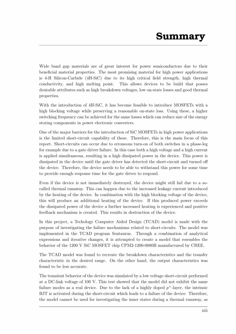
Wide band gap materials are of great interest for power semiconductors due to theirbeneficial material properties. The most promising material for high power applicationsis 4-H Silicon-Carbide (4H-SiC) due to its high critical field strength, high thermalconductivity, and high melting point. This allows devices to be build that possesdesirable attributes such as high breakdown voltages, low on-state losses and good thermalproperties.
With the introduction of 4H-SiC, it has become feasible to introduce MOSFETs with ahigh blocking voltage while preserving a reasonable on-state loss. Using these, a higherswitching frequency can be achieved for the same losses which can reduce size of the energystoring components in power electronic converters.
One of the major barriers for the introduction of SiC MOSFETs in high power applicationsis the limited short-circuit capability of these. Therefore, this is the main focus of thisreport. Short-circuits can occur due to erroneous turn-on of both switches in a phase-legfor example due to a gate driver failure. In this case both a high voltage and a high currentis applied simultaneous, resulting in a high dissipated power in the device. This power isdissipated in the device until the gate driver has detected the short-circuit and turned offthe device. Therefore, the device needs to be able to withstand this power for some timeto provide enough response time for the gate driver to respond.
Even if the device is not immediately destroyed, the device might still fail due to a so-called thermal runaway. This can happen due to the increased leakage current introducedby the heating of the device. In combination with the high blocking voltage of the device,this will produce an additional heating of the device. If this produced power exceedsthe dissipated power of the device a further increased heating is experienced and positivefeedback mechanism is created. This results in destruction of the device.
In this project, a Techology Computer Aided Design (TCAD) model is made with thepurpose of investigating the failure mechanisms related to short-circuits. The model wasimplemented in the TCAD program Sentaurus. Through a combination of analyticalexpressions and iterative changes, it is attempted to create a model that resembles thebehavior of the 1200 V SiC MOSFET chip CPM2-1200-0080B manufactured by CREE.
The TCAD model was found to recreate the breakdown characteristics and the transfercharacteristic in the desired range. On the other hand, the output characteristics wasfound to be less accurate.
The transient behavior of the device was simulated by a low voltage short-circuit performedat a DC-link voltage of 100 V. This test showed that the model did not exhibit the samefailure modes as a real device. Due to the lack of a highly doped p`-layer, the intrinsicBJT is activated during the short-circuit which leads to a failure of the device. Therefore,the model cannot be used for investigating the inner states during a thermal runaway, as
xiii

PED4-1043 Table of Contents
it fails due to the activation of the intrinsic BJT at an earlier stage.
xiv

Introduction 1In this chapter, the motivation for this project is presented. The importance of powersemiconductors is introduced and the reasoning for changing from Si-based semiconductorsto SiC is presented.
1.1 Introduction to Power Semiconductors
With the increasing use of renewable energy sources, the number of power convertersare increasing. Therefore, the reliability and efficiency of these converters are of greatconcern[4]. It is estimated that by 2020, the total installed capacity of wind power willbe approximately 760 GW, and the largest wind turbines will be rated for more than 10MW[5].
Power semiconductors are one of the main components of power converters and thereforealso the efficiency and reliability of these components are of great interest as they play amajor role in the overall reliability of the power converters.
The semiconductors used for high power applications, such as wind power converters, areoften based on Silicon (Si). However, Si-based devices have limitations when it comes toblocking voltage capability, operation temperature, and switching speed. Wide Bandgap(WBG) devices such as Gallium Nitride (GaN), or Silicon Carbide (SiC), are starting tobe used as they provide better performance than the commonly used Si-based devices.Therefore, WBG-devices are expected to enter the market in the near future to achievesmaller and more efficient power converters[6].
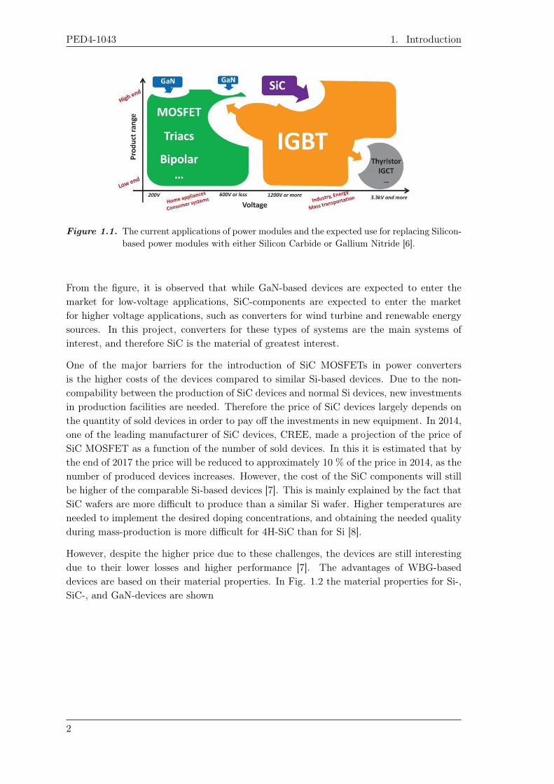
In Fig. 1.1, the common application of different types of power modules is presented.
1
PED4-1043 1. Introduction
Figure 1.1. The current applications of power modules and the expected use for replacing Silicon-based power modules with either Silicon Carbide or Gallium Nitride [6].
From the figure, it is observed that while GaN-based devices are expected to enter themarket for low-voltage applications, SiC-components are expected to enter the marketfor higher voltage applications, such as converters for wind turbine and renewable energysources. In this project, converters for these types of systems are the main systems ofinterest, and therefore SiC is the material of greatest interest.
One of the major barriers for the introduction of SiC MOSFETs in power convertersis the higher costs of the devices compared to similar Si-based devices. Due to the non-compability between the production of SiC devices and normal Si devices, new investmentsin production facilities are needed. Therefore the price of SiC devices largely depends onthe quantity of sold devices in order to pay off the investments in new equipment. In 2014,one of the leading manufacturer of SiC devices, CREE, made a projection of the price ofSiC MOSFET as a function of the number of sold devices. In this it is estimated that bythe end of 2017 the price will be reduced to approximately 10 % of the price in 2014, as thenumber of produced devices increases. However, the cost of the SiC components will stillbe higher of the comparable Si-based devices [7]. This is mainly explained by the fact thatSiC wafers are more difficult to produce than a similar Si wafer. Higher temperatures areneeded to implement the desired doping concentrations, and obtaining the needed qualityduring mass-production is more difficult for 4H-SiC than for Si [8].
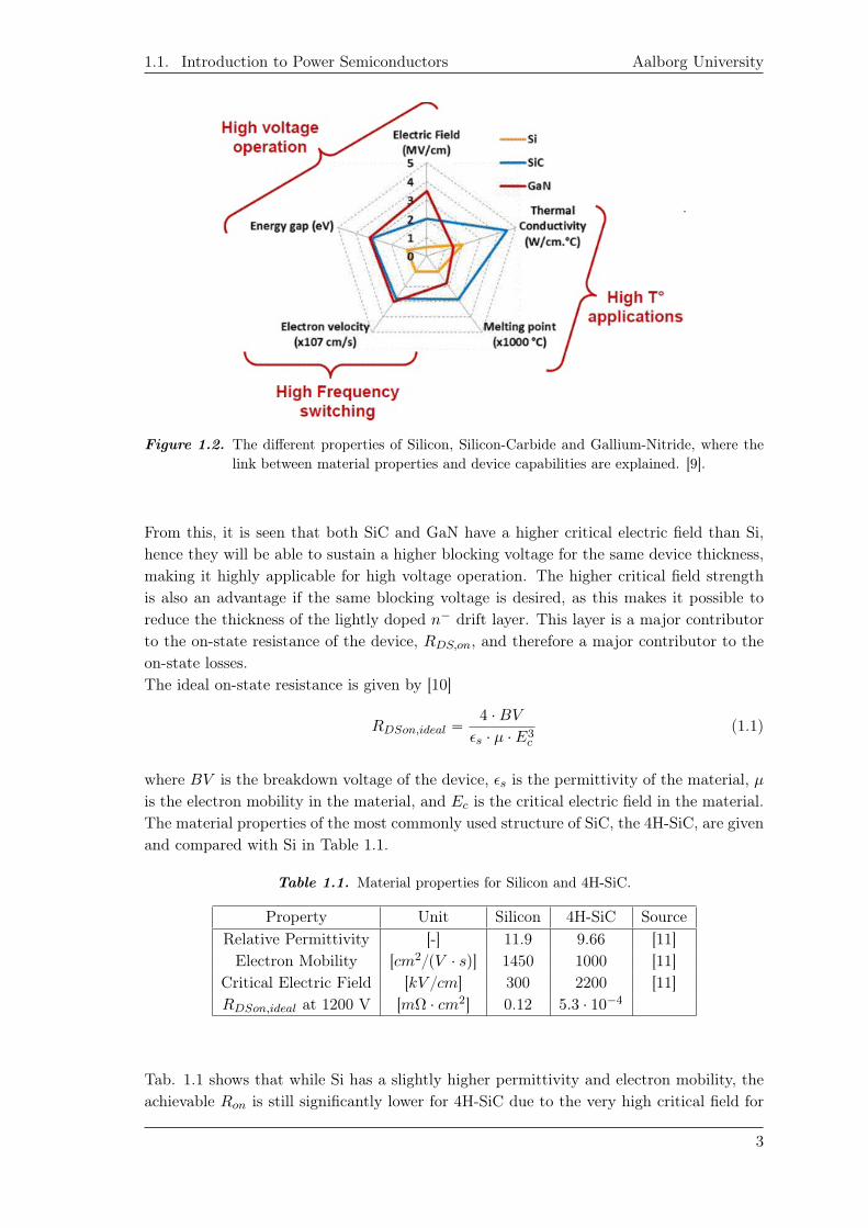
However, despite the higher price due to these challenges, the devices are still interestingdue to their lower losses and higher performance [7]. The advantages of WBG-baseddevices are based on their material properties. In Fig. 1.2 the material properties for Si-,SiC-, and GaN-devices are shown
2
1.1. Introduction to Power Semiconductors Aalborg University
Figure 1.2. The different properties of Silicon, Silicon-Carbide and Gallium-Nitride, where thelink between material properties and device capabilities are explained. [9].
From this, it is seen that both SiC and GaN have a higher critical electric field than Si,hence they will be able to sustain a higher blocking voltage for the same device thickness,making it highly applicable for high voltage operation. The higher critical field strengthis also an advantage if the same blocking voltage is desired, as this makes it possible toreduce the thickness of the lightly doped n´ drift layer. This layer is a major contributorto the on-state resistance of the device, RDS,on, and therefore a major contributor to theon-state losses.The ideal on-state resistance is given by [10]
RDSon,ideal “4 ¨BV
εs ¨ µ ¨ E3c
(1.1)
where BV is the breakdown voltage of the device, εs is the permittivity of the material, µis the electron mobility in the material, and Ec is the critical electric field in the material.The material properties of the most commonly used structure of SiC, the 4H-SiC, are givenand compared with Si in Table 1.1.
Table 1.1. Material properties for Silicon and 4H-SiC.
Property Unit Silicon 4H-SiC SourceRelative Permittivity [-] 11.9 9.66 [11]Electron Mobility [cm2pV ¨ sq] 1450 1000 [11]
Critical Electric Field [kV cm] 300 2200 [11]RDSon,ideal at 1200 V [mΩ ¨ cm2] 0.12 5.3 ¨ 10´4
Tab. 1.1 shows that while Si has a slightly higher permittivity and electron mobility, theachievable Ron is still significantly lower for 4H-SiC due to the very high critical field for
3
PED4-1043 1. Introduction
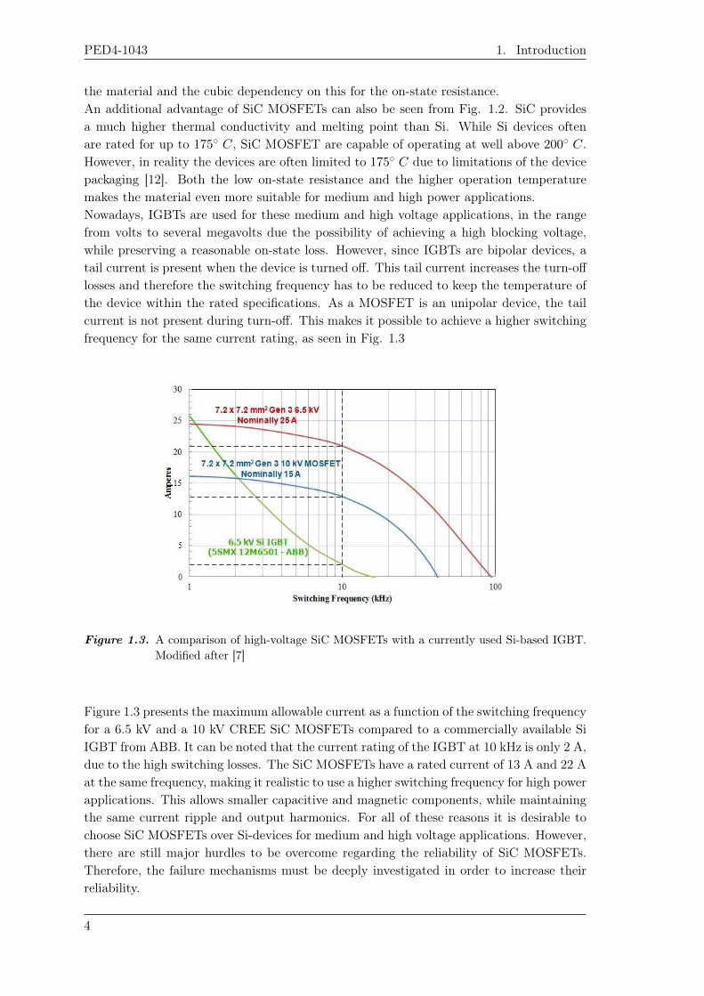
the material and the cubic dependency on this for the on-state resistance.An additional advantage of SiC MOSFETs can also be seen from Fig. 1.2. SiC providesa much higher thermal conductivity and melting point than Si. While Si devices oftenare rated for up to 175˝ C, SiC MOSFET are capable of operating at well above 200˝ C.However, in reality the devices are often limited to 175˝ C due to limitations of the devicepackaging [12]. Both the low on-state resistance and the higher operation temperaturemakes the material even more suitable for medium and high power applications.Nowadays, IGBTs are used for these medium and high voltage applications, in the rangefrom volts to several megavolts due the possibility of achieving a high blocking voltage,while preserving a reasonable on-state loss. However, since IGBTs are bipolar devices, atail current is present when the device is turned off. This tail current increases the turn-offlosses and therefore the switching frequency has to be reduced to keep the temperature ofthe device within the rated specifications. As a MOSFET is an unipolar device, the tailcurrent is not present during turn-off. This makes it possible to achieve a higher switchingfrequency for the same current rating, as seen in Fig. 1.3
Figure 1.3. A comparison of high-voltage SiC MOSFETs with a currently used Si-based IGBT.Modified after [7]
Figure 1.3 presents the maximum allowable current as a function of the switching frequencyfor a 6.5 kV and a 10 kV CREE SiC MOSFETs compared to a commercially available SiIGBT from ABB. It can be noted that the current rating of the IGBT at 10 kHz is only 2 A,due to the high switching losses. The SiC MOSFETs have a rated current of 13 A and 22 Aat the same frequency, making it realistic to use a higher switching frequency for high powerapplications. This allows smaller capacitive and magnetic components, while maintainingthe same current ripple and output harmonics. For all of these reasons it is desirable tochoose SiC MOSFETs over Si-devices for medium and high voltage applications. However,there are still major hurdles to be overcome regarding the reliability of SiC MOSFETs.Therefore, the failure mechanisms must be deeply investigated in order to increase theirreliability.
4

1.2. Motivation of this work Aalborg University
1.2 Motivation of this work
One of the barriers for the use of SiC MOSFETs in high power applications is the reliabilityof these during short-circuit. Due to the low short-circuit withstand time, the MOSFETsare susceptible to failures under these conditions which limits the operational lifetime ofthe devices in high-power applications.As it is desired to implement SiC MOSFET in high-power applications in the future, theseissues need to be solved. The first step towards solving the issue is to understand thefailure mechanism of these devices, and the internal behavior.Furthermore, if a model can be built which represents the real device, it could be possible topredict the behavior of this device during more complex situations. Examples of this couldbe the short-circuit capability of multiple devices in parallel, or the impact of degradationof the modules.
1.3 Problem statement
The purpose of this project is to understand the failure mechanisms of SiC MOSFETsduring short circuit conditions. To understand these mechanisms, it is desired to have amodel that links the external behavior of the device exposed to a short-circuit to the innerphysical mechanisms during these conditions.
Therefore, a 2D Technology Computer Aided Design (TCAD) model is built in the FEMprogram Sentaurus to study the operation of a MOSFET during short-circuit conditions.Using this model, the physical mechanisms of the MOSFET will be simulated, to show thecurrent distribution, electric field variation, temperature, etc. which would not be possibleto observe by experimental results.This knowledge can be used to understand which parameters that affect the reliability ofSiC MOSFETs during short-circuit conditions.
1.3.1 Limitations
As the actual geometry of the MOSFET is unknown, a simplified model is built basedon the parameters given in datasheet of the device. To simplify this model, certainassumptions are made:
• The actual geometry is unknown, therefore the device only resembles the performanceof the real device
• The influence of material defects such as interface traps will be neglected• The influence of the packaging on the thermal properties will be omitted• To reduce the computational complexity, the device is assumed to be symmetric so
that a 2D model can be build. Furthermore, only a halfcell is simulated to reducethe need for computational power.
1.4 Overview of report
In this section the advantages of SiC MOSFETs were introduced, and the motivationfor modeling the short-circuit behavior of these during short-circuits were discussed.
5
PED4-1043 1. Introduction
Furthermore, the problem statement was presented and the limitations of the projectwere introduced.
In the following chapter, the theory about MOSFET as a device will be presented. Thephysical structure of a MOSFET and the typical IV-characteristics will be explained.Additionally, the internal resistances of the MOSFET will be presented, and their influenceduring normal operation and short-circuit will be discussed.
In Chapter 3, the TCAD model is introduced, and the different doping concentrations areeither analytically derived or found through a series of iterations. At first, the breakdowncharacteristics are modeled, then the doping level and the depth of the device is modifiedto obtain the correct IV-characteristics. Finally, the different characteristics of the finaldevice is presented.
Chapter 4 describes the behavior of MOSFETs during a short-circuit of type 1. In thischapter the failure mechanisms of a MOSFET subject to a short-circuit is discussed, andthe difference between different types of failure is explained.
This knowledge is used in Chapter 5, where a short-circuit is simulated using the TCADmodel described in Chapter 3. However, due to simplifications of the model, other failuremodes than thermal runaway is encountered. This failure mode is investigated and possiblesolutions are suggested. However, none of these are implemented.
Finally, in Chapter 6 the conclusions are drawn and Chapter 7 discusses the limitationsand challenges of this project. In this, the implications of the different assumptions of theproject are discussed, and some suggestions for improvement of the project is given.
6
MOSFET theory 2Metal Oxide Semiconductor Field Effect Transistors (MOSFETs) are often used for lowvoltage power electronic circuits. However, with the introduction of SiC it has becomerealistic to manufacture power MOSFET with the necessary breakdown voltage for highpower application while still maintaining relatively low on-state losses. In this section, thestructure and working principle of the power MOSFET will be described.
2.1 Device overview
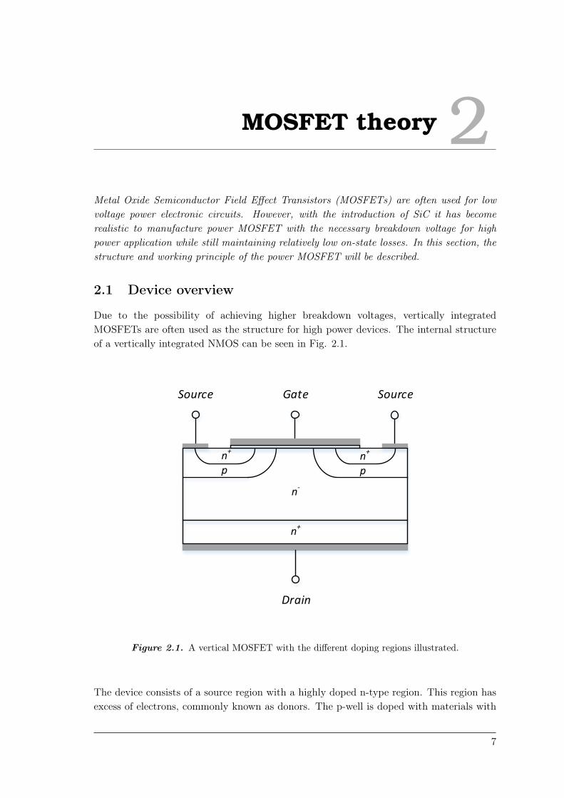
Due to the possibility of achieving higher breakdown voltages, vertically integratedMOSFETs are often used as the structure for high power devices. The internal structureof a vertically integrated NMOS can be seen in Fig. 2.1.
n-
n+
n+
p
Source SourceGate
Drain
n+
p
Figure 2.1. A vertical MOSFET with the different doping regions illustrated.
The device consists of a source region with a highly doped n-type region. This region hasexcess of electrons, commonly known as donors. The p-well is doped with materials with
7
PED4-1043 2. MOSFET theory
a lack of electrons, also known as an excess of holes. These are denoted as acceptors orp-type material. To adjust the breakdown voltage of the device, a layer of lightly doped n-type material is used. This region is known as the drift region. Finally, the device consistsof a drain region which has a high concentration of n-type material, named the substrate.
The flow of current between the two power terminals, drain and source, is controlled bythe applied voltage at the gate terminal with respect to the source terminal, ie. the gate-source voltage VGS . When a positive voltage is applied across these terminals, an electricfield is applied and a channel for conduction of electrons is formed through the p-well.The IV-characteristics of the MOSFET depends on the applied gate voltage, VGS , and theapplied voltage across the power terminals, VDS . For the case where VGS is lower than thethreshold voltage, VT , the MOSFET is in its off-state. If a positive drain-source voltageis applied,VDS > 0, ideally the MOSFET will not be conducting any current. In reality, asmall leakage current will be present.
When a gate voltage greater than the threshold voltage is applied, VGS > VT , a channelin the p-well is formed and the current will start to flow. As the voltage is increased, thewidth of this channel is increased causing the channel to be more conductive.
2.2 IV-characteristics
From the properties of the gate-channel the following equation can be derived for the draincurrent for an when the device operates in its linear range [11]
ID “ µ ¨Wchannel
Lchannel¨Cox
2¨ r2 ¨ pVGS ´ VT q ¨ VDS ´ V
2DSs (2.1)
where µ is the channel mobility, Wchannel is the out of plane width of the channel, Lchannel
is the channel length, and Cox is the per area capacitance of the gate. Eq. 2.1 is oftensimplified by assuming the device to be in one of two states. When the drain-source voltageis small the channel is not fully saturated and the device is in its linear mode. When thedrain-source voltage is large, the channel is assumed to be fully saturated and an increasein drain-source voltage will not result in a further increase of the drain current.
When VDS is small, the MOSFET is the linear region. In this region, the drain-sourcevoltage can be assumed to be small; hence the term V 2
DS can be neglected [10]. Therefore,the IV-characteristic in the linear region can be approximated by
ID “ µ ¨Wchannel
Lchannel¨ Cox ¨ pVGS ´ VT q ¨ VDS (2.2)
From this equation, the equivalent resistance of the MOSFET in the linear region can befound as the increase in the drain-source voltage when the drain current increases
Ron “dVDS
dID“
Lchannel
µ ¨Wchannel ¨ Cox ¨ pVGS ´ VT q(2.3)
From these expressions, it can be seen that the resistance of the MOSFET depend onmaterial properties, device geometry, and the applied gate voltage. As the drain-source
8
2.2. IV-characteristics Aalborg University
voltage increases, the channel will saturate and the drain current will no longer increaseas VDS is increased. The condition were this occurs can be found from the point wherethe derivative of the drain current with respect to the drain-source voltage is zero. Thesolution to this equation is the so-called pinch-off condition, which is the voltage at whichthe MOSFET is saturated. This is given by
VDS “ VGS ´ VT (2.4)
In the saturation region the current can be found by considering the drain-source voltage tobe fixed at the pinch of voltage. Substituting VDS “ VGS´VT into Eq. 2.1, the saturationcurrent can be found by
ID “Wchannel ¨ µ ¨ Cox
2 ¨ Lchannel¨ pVGS ´ VT q
2 (2.5)
whereFrom Eq. 2.5, the current is seen to be independent of the drain-source voltage once thechannel is fully saturated. This is under the assumption that the channel shape is notaffected by the drain-source voltage. In reality, a small increase in the output currentis seen due to the changes in the shape of the channel when the drain-source voltage isincreased [10].
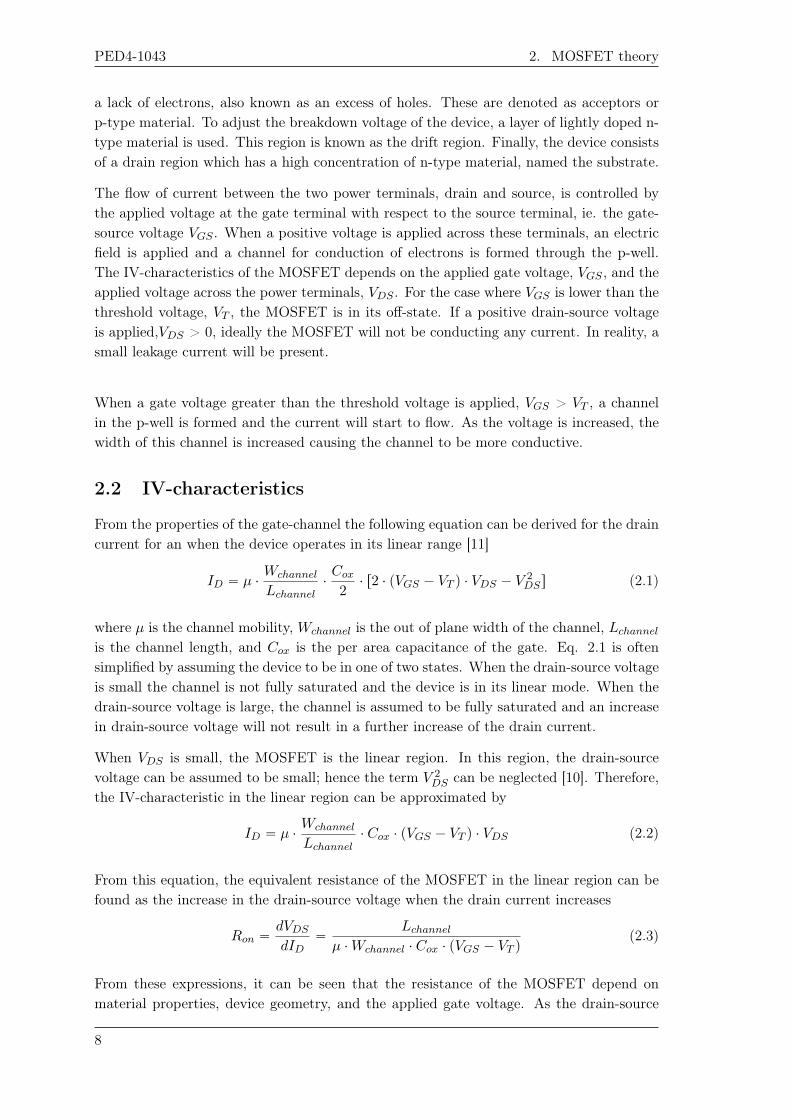
As seen from the equations Eq. 2.2, Eq. 2.4, and Eq. 2.5 the drain current and thetransition between the linear region and the saturation region depends on the applied gatevoltage. Fig. 2.2 shows the output characteristics of a device at different gate voltages.
Figure 2.2. The output characteristics of a MOSFET at different gate voltages. The dashed lineindicates the crossover from the linear region to the saturation region [10].
The dashed line in Fig. 2.2, the drain-source voltage where pinch-off occurs increases asthe gate voltage increases.
9
PED4-1043 2. MOSFET theory
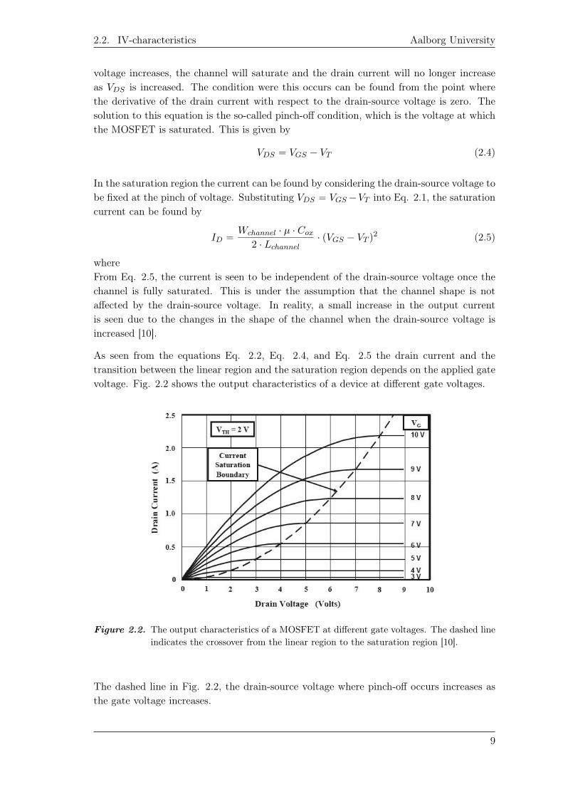
The transfer characteristics of the MOSFET can be observed in Fig. 2.2. This is thecurrent as a function of the applied gate voltage, when the drain-source voltage is fixed.An example of the transfer characteristics of an arbitrary power MOSFET is shown in Fig.2.3
Figure 2.3. The transfer characteristic of an arbitrary power MOSFET [13]
The slope of the drain current versus the gate-source voltage is known as thetransconductance of the device, g. This slope is found from the MOSFET IV-characteristicsat a constant VDS using the previously shown equation for the drain current. In the linearregion the transconductance can be found by
g “dIDdVGS
“ µ ¨Wchannel
Lchannel¨ Cox ¨ VDS (2.6)
Here it is noted that the transconductance depends on approximately the same parametersas the on-state resistance, hence the two parameters both have to be considered whenmodeling the MOSFET structure in Chapter 3.
2.3 Internal Resistances of the MOSFET
All of the internal resistances of the device both influence the on-state behavior of thedevice, and the behavior during a short-circuit, and therefore the origin of these resistanceswill be explained in this section.
The internal resistance of a MOSFET, Ron, can be divided into four major contributors.These different terms are given by [14].
10
2.3. Internal Resistances of the MOSFET Aalborg University
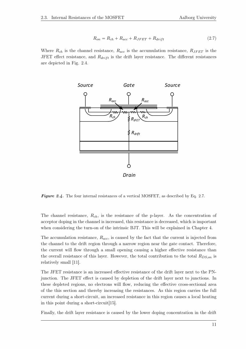
Ron “ Rch `Racc `RJFET `Rdrift (2.7)
Where Rch is the channel resistance, Racc is the accumulation resistance, RJFET is theJFET effect resistance, and Rdrift is the drift layer resistance. The different resistancesare depicted in Fig. 2.4.
Source SourceGate
Drain
RJFETRch
Racc
Rdrift
Racc
Rch
Figure 2.4. The four internal resistances of a vertical MOSFET, as described by Eq. 2.7.
The channel resistance, Rch, is the resistance of the p-layer. As the concentration ofacceptor doping in the channel is increased, this resistance is decreased, which is importantwhen considering the turn-on of the intrinsic BJT. This will be explained in Chapter 4.
The accumulation resistance, Racc, is caused by the fact that the current is injected fromthe channel to the drift region through a narrow region near the gate contact. Therefore,the current will flow through a small opening causing a higher effective resistance thanthe overall resistance of this layer. However, the total contribution to the total RDS,on isrelatively small [11].
The JFET resistance is an increased effective resistance of the drift layer next to the PN-junction. The JFET effect is caused by depletion of the drift layer next to junctions. Inthese depleted regions, no electrons will flow, reducing the effective cross-sectional areaof the this section and thereby increasing the resistances. As this region carries the fullcurrent during a short-circuit, an increased resistance in this region causes a local heatingin this point during a short-circuit[15].
Finally, the drift layer resistance is caused by the lower doping concentration in the drift
11

PED4-1043 2. MOSFET theory
layer. This layer is needed to obtain the desired voltage rating. As the voltage rating ofthe device is increased the thickness of the drift layer has to be increased to achieve theneeded breakdown voltage, increasing the drift region resistance. [14]
12

Description of Model 3To investigate the effects of short-circuits, it is desired to build a TCAD model of the chipunder investigation, the SiC MOSFET CPM2-1200-0080B from Cree [16]. In this chapter,the dimensions and doping profiles of the TCAD model will be described.
3.1 Geometry of Model
As the geometry of the device under investigations is unknown, the geometry is inspiredby a model made by Romano et. al. [15], which consider the same device but in a previousgeneration. The main takeaway from this model is the width of the device, 8.7µm whichwill be considered to be the fixed width of the device. Furthermore, the width and shapeof the source and channel region from this device will be used. The borders of this half-cellwithout doping concentrations is shown in Fig. 3.1.
Figure 3.1. The geometry used for these investigations. All dimensions are in µm.
With this starting point, the different geometries and doping concentrations of the deviceis modeled through a combination of analytical calculations and iterations.
13
PED4-1043 3. Description of Model
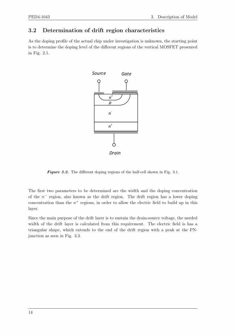
3.2 Determination of drift region characteristics
As the doping profile of the actual chip under investigation is unknown, the starting pointis to determine the doping level of the different regions of the vertical MOSFET presentedin Fig. 2.1.
n-
n+
Source Gate
Drain
pn+
Figure 3.2. The different doping regions of the half-cell shown in Fig. 3.1.
The first two parameters to be determined are the width and the doping concentrationof the n´ region, also known as the drift region. The drift region has a lower dopingconcentration than the n` regions, in order to allow the electric field to build up in thislayer.
Since the main purpose of the drift layer is to sustain the drain-source voltage, the neededwidth of the drift layer is calculated from this requirement. The electric field is has atriangular shape, which extends to the end of the drift region with a peak at the PN-junction as seen in Fig. 3.3.
14

3.2. Determination of drift region characteristics Aalborg University
p n- n+
w x
Ec
E
Figure 3.3. The desired shape of the electric field, when a reverse voltage of 1200 V is applied.
The applied voltage can be found from the integral of the electric field. As seen from Fig.3.3, the desired electric field is triangular, thus the integral of this electric field can befound from
V “E ¨ w
2(3.1)
The amplitude of the electric field should not exceed the critical electric field for 4H-SiC,in order to avoid the breakdown of the device. Therefore, the needed drift region widthcan be calculated from
w “2 ¨BV
Ec(3.2)
where BV is the desired breakdown voltage, 1200 V for the device considered in this work,and Ec is the critical electric field for 4H-SiC at 300 K , 2.2 ¨ 106 V cm [11]. From this,the needed width in order to obtain a breakdown voltage of 1200 V has been found to be10.9 µm.
To ensure that the electric field extends to the end of the drift region when the appliedvoltage is at the breakdown voltage, the doping concentration of drift region must beadjusted to obtain the needed slope of the electric field. The decrease in the electric fieldcan be found from Gauss’ Law in one dimension [17].
dE
dx“ρ
ε(3.3)
where dEdx is the slope of the electric field along the drift region, ρ is the charge density, and
ε is the total permittivity of the region. Assuming that a constant doping concentrationacross the entire drift region, the charge density will be ´q ¨Nd, where the sign is causedby the negative charge of electrons. The permittivity will be the permittivity of 4H-SiC.The slope of the electric field per unit width can then be found by
dE
dx“ ´
q ¨Nd
εr ¨ ε0(3.4)
15
PED4-1043 3. Description of Model
where q is the elementary charge 1.6 ¨ 10´19 C, Nd is the doping concentration of the driftregion, εs is the relative permittivity of 4H-SiC 9.66, and ε0 is the vacuum permeability8.85 ¨ 10´14 F cm.To ensure that the electric field is zero by the end of the drift region, the dopingconcentration is found by
Ec ´q ¨Nd
εr ¨ ε0¨ w “ 0 (3.5)
which can be rearranged to
Nd “Ec ¨ εr ¨ ε0q ¨ w
(3.6)
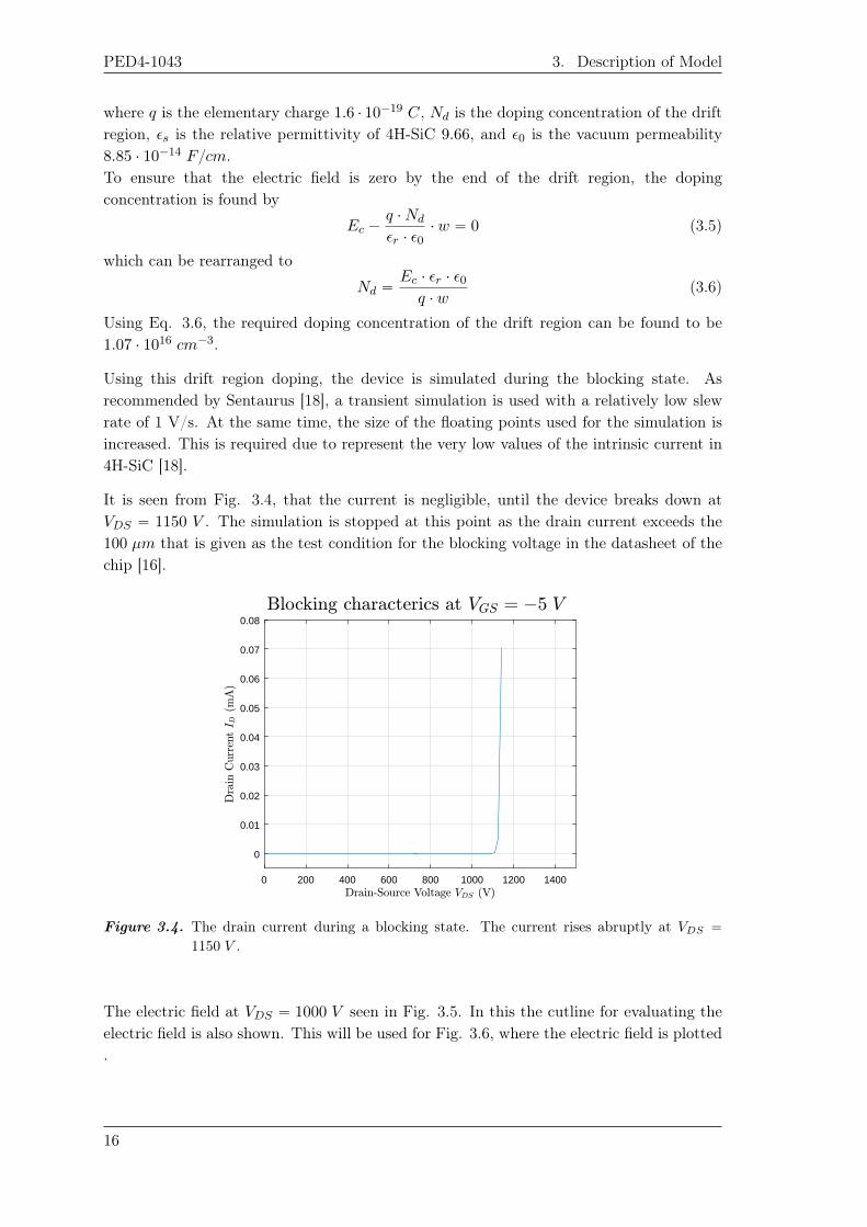
Using Eq. 3.6, the required doping concentration of the drift region can be found to be1.07 ¨ 1016 cm´3.
Using this drift region doping, the device is simulated during the blocking state. Asrecommended by Sentaurus [18], a transient simulation is used with a relatively low slewrate of 1 V/s. At the same time, the size of the floating points used for the simulation isincreased. This is required due to represent the very low values of the intrinsic current in4H-SiC [18].
It is seen from Fig. 3.4, that the current is negligible, until the device breaks down atVDS “ 1150 V . The simulation is stopped at this point as the drain current exceeds the100 µm that is given as the test condition for the blocking voltage in the datasheet of thechip [16].
0 200 400 600 800 1000 1200 1400Drain-Source Voltage VDS (V)
0
0.01
0.02
0.03
0.04
0.05
0.06
0.07
0.08
Dra
inCurr
entI D
(mA
)
Blocking characterics at VGS = !5 V
Figure 3.4. The drain current during a blocking state. The current rises abruptly at VDS “
1150 V .
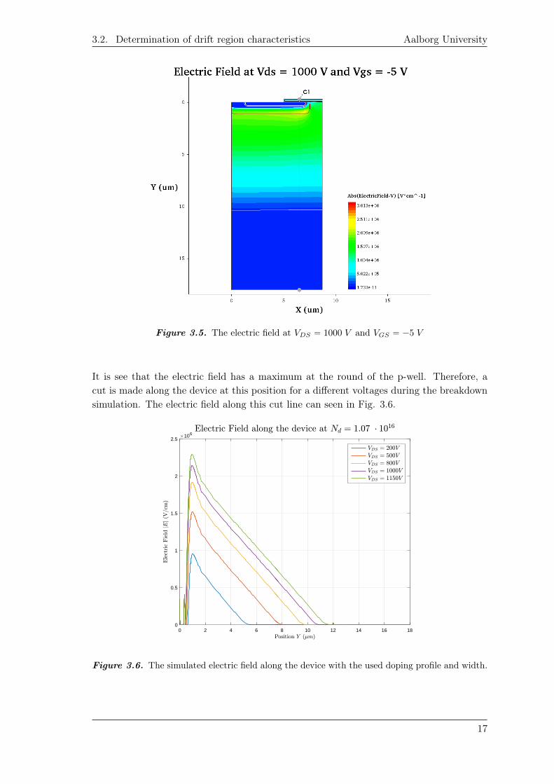
The electric field at VDS “ 1000 V seen in Fig. 3.5. In this the cutline for evaluating theelectric field is also shown. This will be used for Fig. 3.6, where the electric field is plotted.
16
3.2. Determination of drift region characteristics Aalborg University
Figure 3.5. The electric field at VDS “ 1000 V and VGS “ ´5 V
It is see that the electric field has a maximum at the round of the p-well. Therefore, acut is made along the device at this position for a different voltages during the breakdownsimulation. The electric field along this cut line can seen in Fig. 3.6.
0 2 4 6 8 10 12 14 16 18Position Y (7m)
0
0.5
1
1.5
2
2.5
Elect
ric
Field
jEj(
V/c
m)
#106Electric Field along the device at Nd = 1:07 " 1016
VDS = 200VVDS = 500VVDS = 800VVDS = 1000VVDS = 1150V
Figure 3.6. The simulated electric field along the device with the used doping profile and width.
17

PED4-1043 3. Description of Model
Two things can be noted from this figure. First of all the electric field at the PN-junctionreaches the critical electric field for 4H-SiC, 2200 kV/cm, at the instance of the breakdown.Secondly, the electric field is zero at the end of the drift region at the point of breakdownas calculated.With this parameter fixed, the next task is to determine the area factor to achieve thedesired current density of the device.
3.3 Calculation of Area Factor
To reduce the computational requirements, the simulated device is a 2D cross-section ofthe full 3D structure. As the current characteristics depends on the out-of-plane width ofthe device, there is a need to account for this simplification of the model. In Sentaurus,this is done by including an area factor, which is the ratio between the simulated topsurface of the chip and the actual surface of the chip.
By default, Sentaurus assumes a device thickness of 1 µm. As the modeled device has awidth of 8.7 µm, this gives a modeled surface area of 8.7 µm2.
The surface of the real device can be found in Fig. 3.7.
Figure 3.7. The surface area of the real device. The black rectangles indicate the areaapproximated as the active area. Modified after [16].
As an approximation, the active area is considered to be the entire surface of the chipneglecting the corners and a small area for the gate connections. This approximatedactive area of the device has a surface area of 6.339 ¨ 106 µm2 and therefore the starting
18
3.4. Determination of Threshold Voltage and Transfer CharacteristicsAalborg University
point for the area factor is
AF “6.339 ¨ 106 µm2
8.7 µm2“ 7.28 ¨ 105 (3.7)
However, as this is a rough approximation, the actual value of the area factor will beadjusted to fit the IV-characteristics of the device.
3.4 Determination of Threshold Voltage and TransferCharacteristics
The next characteristics to consider are the threshold voltage and the transfercharacteristics. The threshold voltage is needed to form the channel, in which the currentcan flow from the drain to the source. The threshold voltage consists of three differentterms due to different barriers that needs to be overcome for the channel to be formed.The equation is given by
VT “ θMS `∆Vox ` Vs (3.8)
The first term due to differences in the so-called work function of the two materials incontact with each other. This is the potential needed to ensure that the potential of thematerials are identical. For simplicity it is often assumed that the two materials have thesame work function, θm “ θs, and therefore θms “ 0.
The second term is the voltage drop across the gate oxide. This voltage drop is proportionalto the surface charge stored at top of the oxide, hence at the interface between the gateoxide and the gate contact.
∆Vox “Qm
εox¨ tox (3.9)
where Qm is the stored charge, εox is the permittivity of the gate oxide, and tox is thethickness of the gate oxide.
The stored charge on the oxide is derived by [11] to be
QM “
c
4 ¨NAεsi ¨ k ¨ T ¨ lnpNA
niq (3.10)
where k is the Boltzmann constant, 1.38066 ¨ 10´23 JK, T is the temperature in Kelvin,NA is the doping concentration of the channel, and ni is the intrinsic current of the device,the current that is flowing when no voltage is applied.Therefore, the voltage drop across the gate oxide can be found from
∆Vox “
b
4 ¨NAεsi ¨ k ¨ T ¨ lnpNAniq
εox¨ tox (3.11)
Substituting the capacitance per unit area Cox “ εoxtox, the voltage drop across the gateoxide can be found to be
∆Vox “
b
4 ¨NAεsi ¨ k ¨ T ¨ lnpNAniq
Cox(3.12)
19
PED4-1043 3. Description of Model
The third term is the voltage needed to raise the potential of the channel region enough tobecome conducting. This is known as strong inversion. The difference in potential energyis derived in [11] to be
∆E “ 2 ¨ k ¨ T ¨ lnpNA
niq (3.13)
This energy is related to the potential energy by
Vs “∆E
q“ 2 ¨
k ¨ T
q¨ lnp
NA
niq (3.14)
where q is the elementary charge.Combining all of these three equations, the final expression ends up being
VT “
b
4 ¨NAεsi ¨ k ¨ T ¨ lnpNAniq
Cox` 2 ¨
k ¨ T
q¨ lnp
NA
niq (3.15)
From this equation, it is seen that for the same temperature, two parameters can be varied:Either the gate capacitance, COX , can be modified or the concentration of acceptor dopingcan be changed.The change of the Cox corresponds to a change in the properties of the gate, such as otherdimensions or the use of a gate material with a higher permittivity. For high voltagedevices, a gate thickness of 50 nm, and the material SiO2, are often used hence theseparameters are not changed.
As the gate properties are fixed, the acceptor doping of the p-well is modified to achievethe desired threshold voltage. As a starting point, a channel doping of NA “ 2 ¨ 1017 cm´3
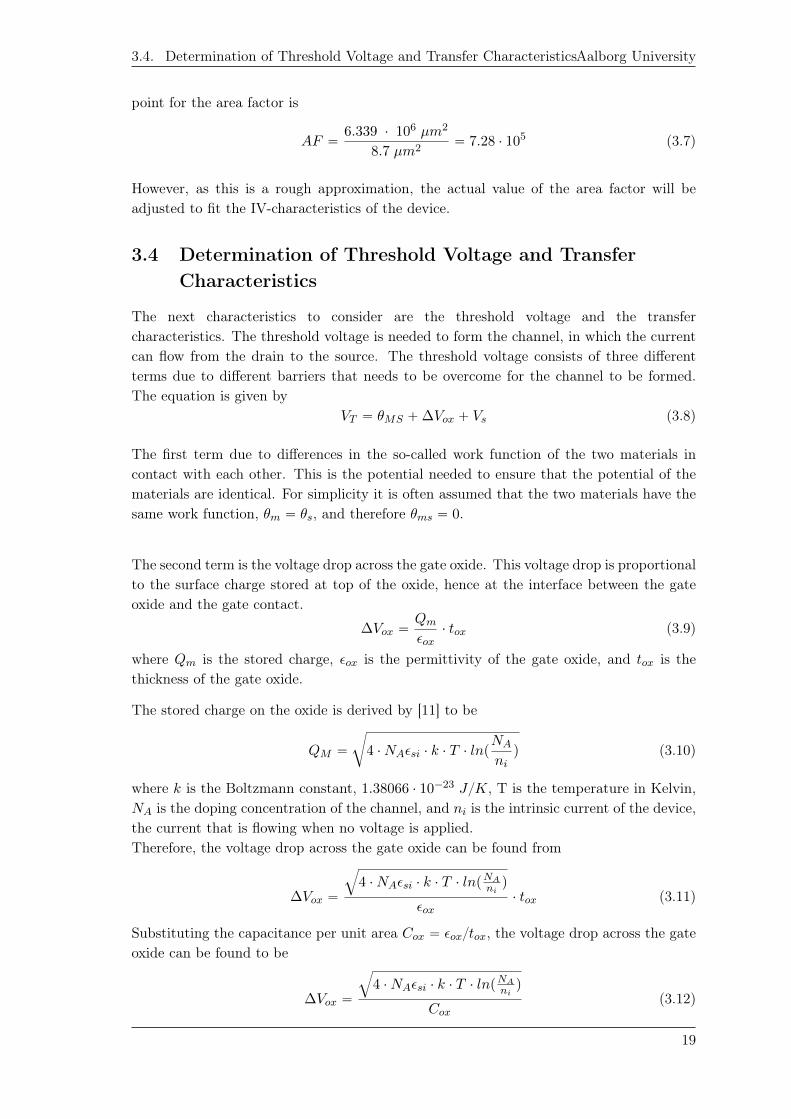
is considered, as this is the value suggested in the original model from Romano et al [15].The resulting transfer characteristic is shown in Fig. 3.8, where the simulated results arecompared with the transfer characteristics given in the datasheet at 25˝ C.
20
3.4. Determination of Threshold Voltage and Transfer CharacteristicsAalborg University
0 2 4 6 8 10Gate-Source Voltage VGS (V)
-10
0
10
20
30
40
50
60
70
80
Dra
inCurr
entI D
(A)
Initial Transfer Characteristics at 25/C
Simulation
Datasheet
Figure 3.8. A comparision of the transfer characteristics of the initial simulation and thedatasheet at 25˝ C.
From this figure, two differences between the simulations and the real device can be seen.The simulated threshold voltage is higher than the threshold voltage of the real device. Atthe same time, the transconductance of the simulated device is higher than the one of thereal device.As explained by Eq. 3.4, the threshold voltage can be lowered by decreasing the dopingconcentration of the channel region. The transconductance can be lowered by changingsome of the parameters in Eq. 2.6. The two parameters that are adjustable are the out-of-plane width of the channel or the length of the channel. From Eq. 2.6 it is noted thatthe transconductance decreases when the out of plane- width of the channel decreases.Therefore, the area factor is modified as this corresponds to decreasing the out-of-planewidth of the device.
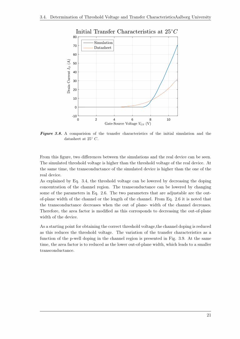
As a starting point for obtaining the correct threshold voltage,the channel doping is reducedas this reduces the threshold voltage. The variation of the transfer characteristics as afunction of the p-well doping in the channel region is presented in Fig. 3.9. At the sametime, the area factor is to reduced as the lower out-of-plane width, which leads to a smallertransconductance.
21
PED4-1043 3. Description of Model
0 2 4 6 8 10Gate-Source Voltage VGS (V)
-10
0
10
20
30
40
50
60
Drain
CurrentI D
(A)
Transfer Characteristics for Various NA at 25/C
NA = 4 " 1017
NA = 5 " 1017
NA = 6 " 1017
Datasheet
Figure 3.9. Variation of the channel doping to achieve the desired transfer characteristics usingan area factor of 3 ¨ 105.
The results of Fig. 3.9 show that the lowered chosen area factor of 3 ¨ 105 results in atransconductance that resembles the real device. It is also seen that a doping concentra-tion between NA “ 5 ¨ 1017 cm´3 and NA “ 6 ¨ 1017 cm´3 give approximately the desiredtransfer characteristics during the on-state of the device when a high gate voltage is ap-plied. However, it is also seen that while the simulated device has a relatively well-definedthreshold voltage, the real device has a lower threshold voltage but does not reach the fulltransconductance before a significantly higher gate voltage is applied.
The difference between the modeled threshold behavior and the datasheet can be explainedby the assumption of a perfect interface between the gate oxide and the 4-H SiC. Non-idealities at this interface is shown in other works to cause shifts in the threshold voltageas presented in Fig. 3.10 [19] .
22
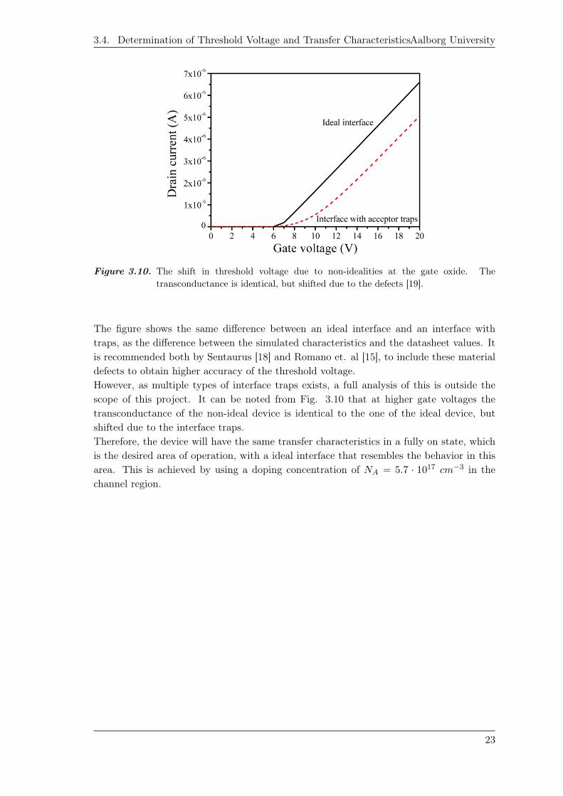
3.4. Determination of Threshold Voltage and Transfer CharacteristicsAalborg University
Figure 3.10. The shift in threshold voltage due to non-idealities at the gate oxide. Thetransconductance is identical, but shifted due to the defects [19].
The figure shows the same difference between an ideal interface and an interface withtraps, as the difference between the simulated characteristics and the datasheet values. Itis recommended both by Sentaurus [18] and Romano et. al [15], to include these materialdefects to obtain higher accuracy of the threshold voltage.However, as multiple types of interface traps exists, a full analysis of this is outside thescope of this project. It can be noted from Fig. 3.10 that at higher gate voltages thetransconductance of the non-ideal device is identical to the one of the ideal device, butshifted due to the interface traps.Therefore, the device will have the same transfer characteristics in a fully on state, whichis the desired area of operation, with a ideal interface that resembles the behavior in thisarea. This is achieved by using a doping concentration of NA “ 5.7 ¨ 1017 cm´3 in thechannel region.
23
PED4-1043 3. Description of Model
0 2 4 6 8 10Gate-Source Voltage VGS (V)
-5
0
5
10
15
20
25
30
35
Dra
inCurr
entI D
(A)
Final Transfer Characteristics at 25/C
Simulation
Datasheet
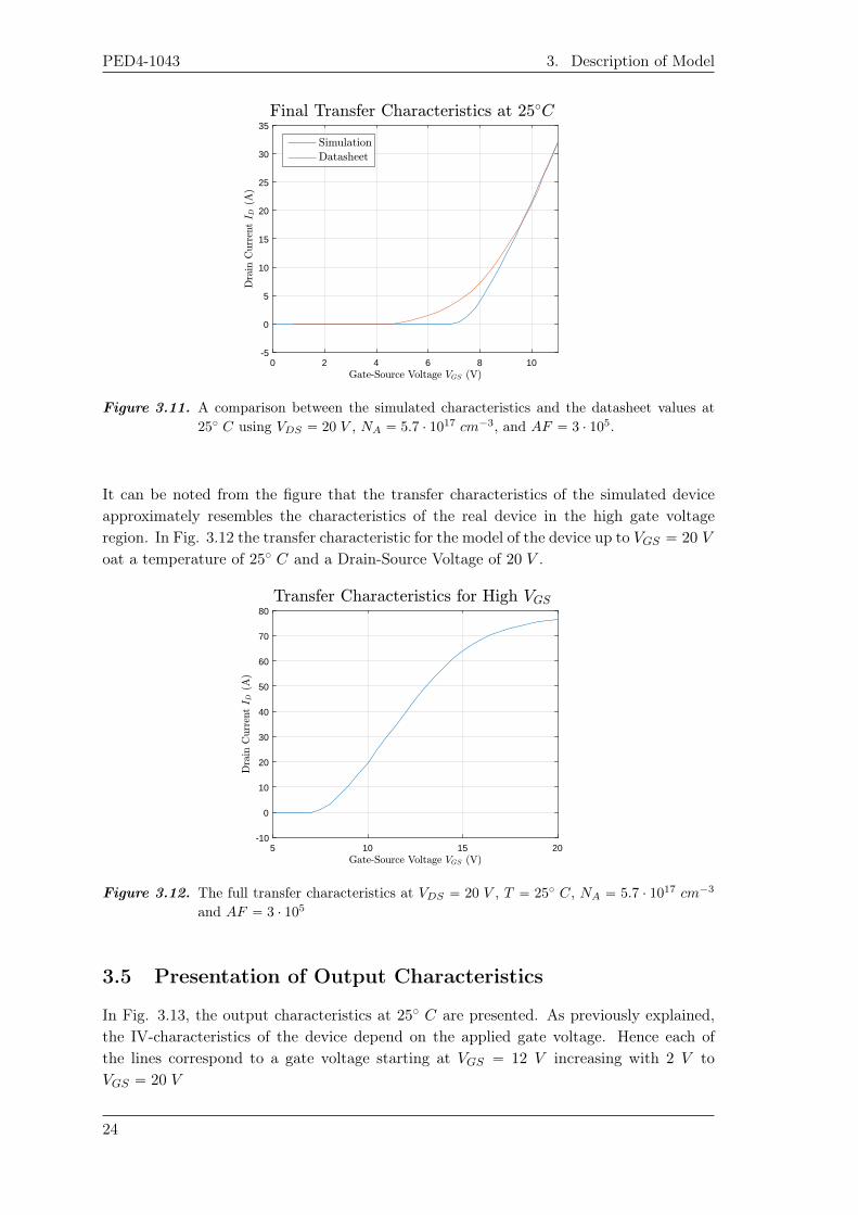
Figure 3.11. A comparison between the simulated characteristics and the datasheet values at25˝ C using VDS “ 20 V , NA “ 5.7 ¨ 1017 cm´3, and AF “ 3 ¨ 105.
It can be noted from the figure that the transfer characteristics of the simulated deviceapproximately resembles the characteristics of the real device in the high gate voltageregion. In Fig. 3.12 the transfer characteristic for the model of the device up to VGS “ 20 V
oat a temperature of 25˝ C and a Drain-Source Voltage of 20 V .
5 10 15 20Gate-Source Voltage VGS (V)
-10
0
10
20
30
40
50
60
70
80
Dra
inCurr
entI D
(A)
Transfer Characteristics for High VGS
Figure 3.12. The full transfer characteristics at VDS “ 20 V , T “ 25˝ C, NA “ 5.7 ¨ 1017 cm´3
and AF “ 3 ¨ 105
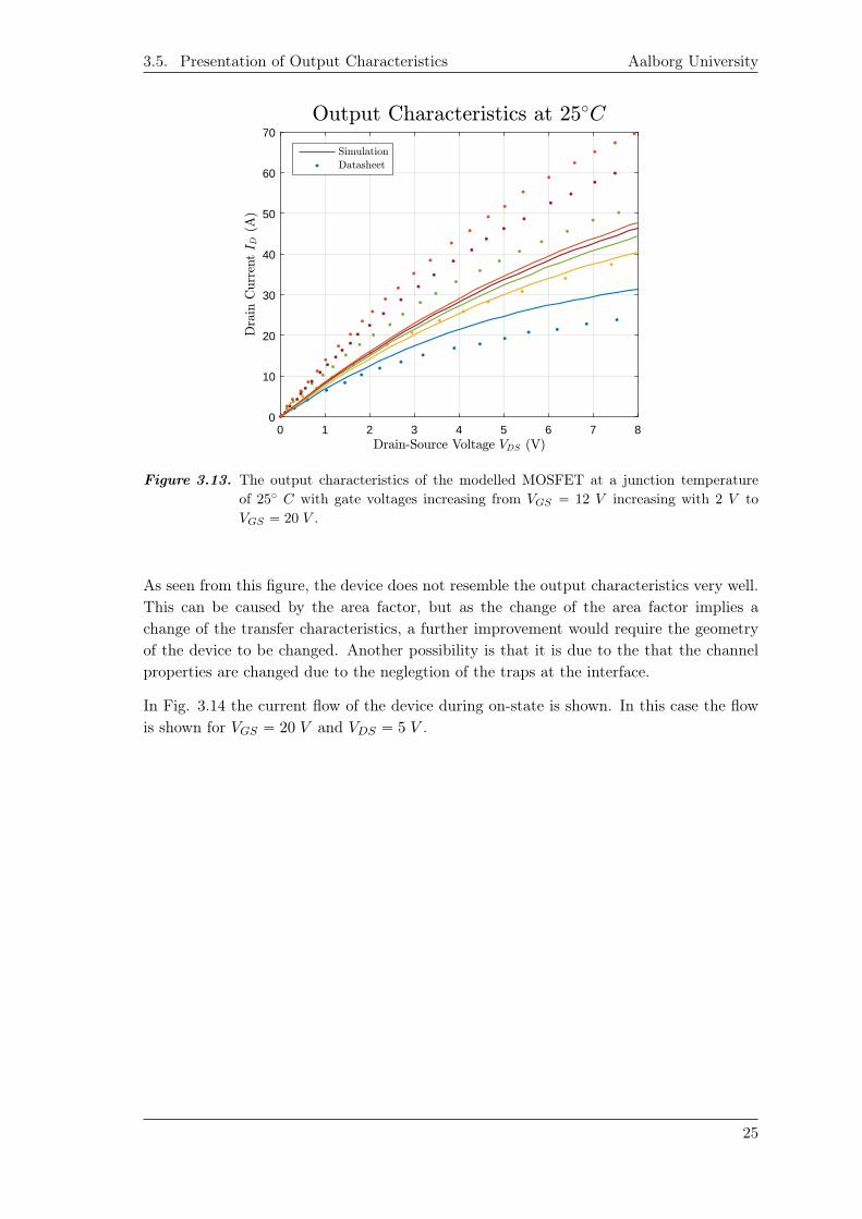
3.5 Presentation of Output Characteristics
In Fig. 3.13, the output characteristics at 25˝ C are presented. As previously explained,the IV-characteristics of the device depend on the applied gate voltage. Hence each ofthe lines correspond to a gate voltage starting at VGS “ 12 V increasing with 2 V toVGS “ 20 V
24
3.5. Presentation of Output Characteristics Aalborg University
0 1 2 3 4 5 6 7 8Drain-Source Voltage VDS (V)
0
10
20
30
40
50
60
70
Dra
inCurr
entI D
(A)
Output Characteristics at 25/C
Simulation
Datasheet
Figure 3.13. The output characteristics of the modelled MOSFET at a junction temperatureof 25˝ C with gate voltages increasing from VGS “ 12 V increasing with 2 V toVGS “ 20 V .
As seen from this figure, the device does not resemble the output characteristics very well.This can be caused by the area factor, but as the change of the area factor implies achange of the transfer characteristics, a further improvement would require the geometryof the device to be changed. Another possibility is that it is due to the that the channelproperties are changed due to the neglegtion of the traps at the interface.
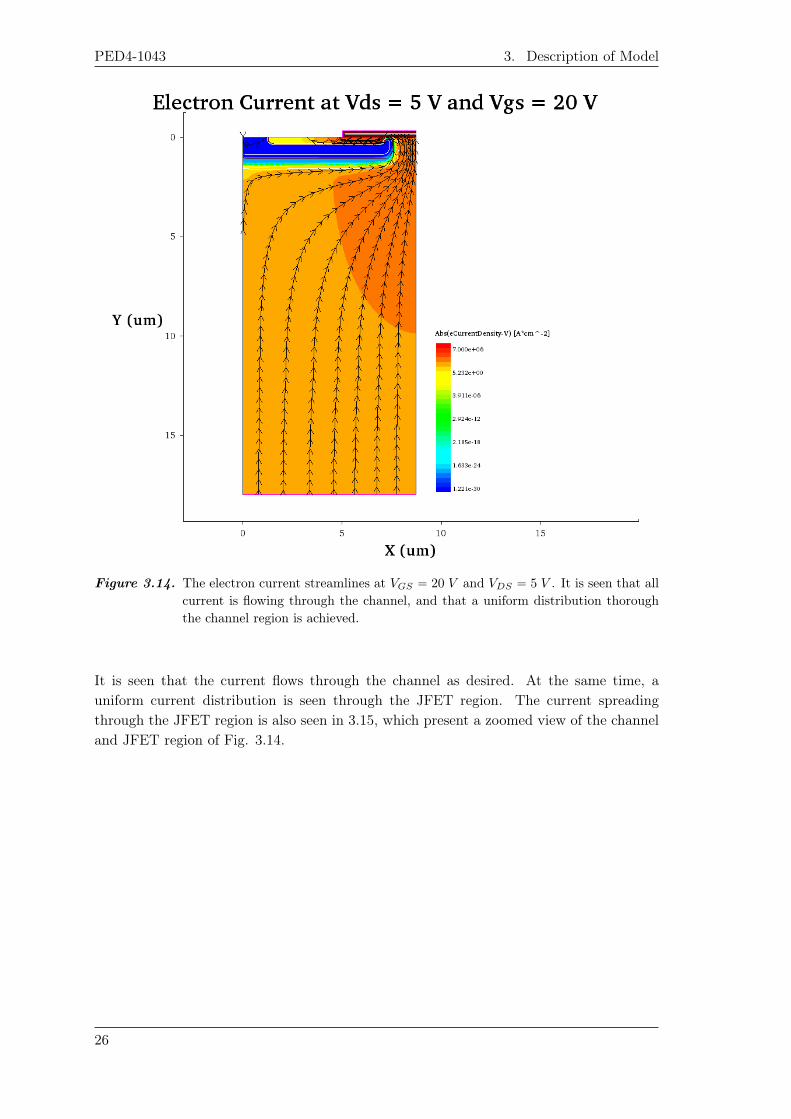
In Fig. 3.14 the current flow of the device during on-state is shown. In this case the flowis shown for VGS “ 20 V and VDS “ 5 V .
25
PED4-1043 3. Description of Model
Figure 3.14. The electron current streamlines at VGS “ 20 V and VDS “ 5 V . It is seen that allcurrent is flowing through the channel, and that a uniform distribution thoroughthe channel region is achieved.
It is seen that the current flows through the channel as desired. At the same time, auniform current distribution is seen through the JFET region. The current spreadingthrough the JFET region is also seen in 3.15, which present a zoomed view of the channeland JFET region of Fig. 3.14.
26
3.5. Presentation of Output Characteristics Aalborg University
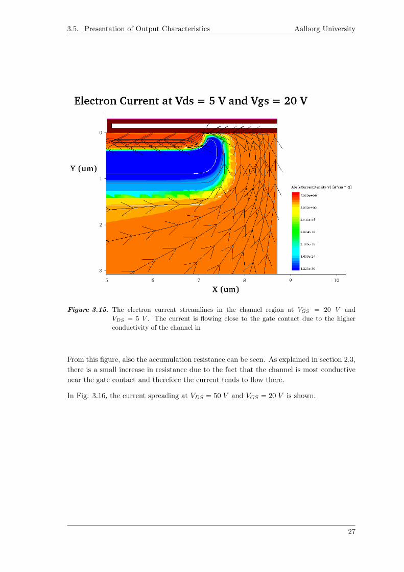
Figure 3.15. The electron current streamlines in the channel region at VGS “ 20 V andVDS “ 5 V . The current is flowing close to the gate contact due to the higherconductivity of the channel in
From this figure, also the accumulation resistance can be seen. As explained in section 2.3,there is a small increase in resistance due to the fact that the channel is most conductivenear the gate contact and therefore the current tends to flow there.
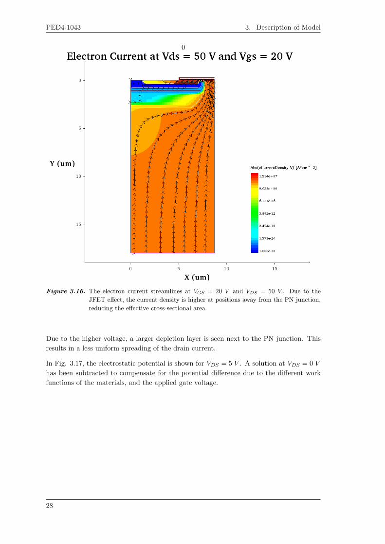
In Fig. 3.16, the current spreading at VDS “ 50 V and VGS “ 20 V is shown.
27
PED4-1043 3. Description of Model
0
Figure 3.16. The electron current streamlines at VGS “ 20 V and VDS “ 50 V . Due to theJFET effect, the current density is higher at positions away from the PN junction,reducing the effective cross-sectional area.
Due to the higher voltage, a larger depletion layer is seen next to the PN junction. Thisresults in a less uniform spreading of the drain current.
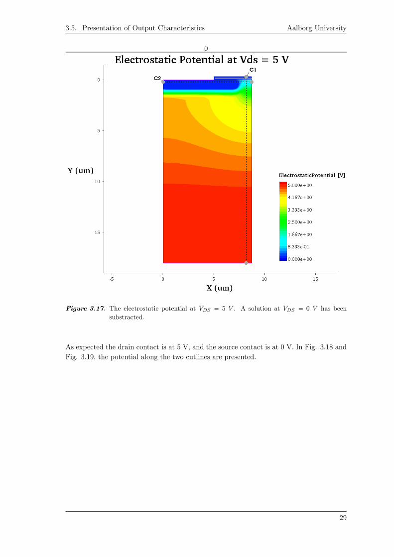
In Fig. 3.17, the electrostatic potential is shown for VDS “ 5 V . A solution at VDS “ 0 V
has been subtracted to compensate for the potential difference due to the different workfunctions of the materials, and the applied gate voltage.
28
3.5. Presentation of Output Characteristics Aalborg University
0
Figure 3.17. The electrostatic potential at VDS “ 5 V . A solution at VDS “ 0 V has beensubstracted.
As expected the drain contact is at 5 V, and the source contact is at 0 V. In Fig. 3.18 andFig. 3.19, the potential along the two cutlines are presented.
29
PED4-1043 3. Description of Model
02 4 6 8 10 12 14 16 18
Y (7m)
0
0.5
1
1.5
2
2.5
3
3.5
4
4.5
5
Pot
ential
(V)
Potential along C1 at VDS = 5V
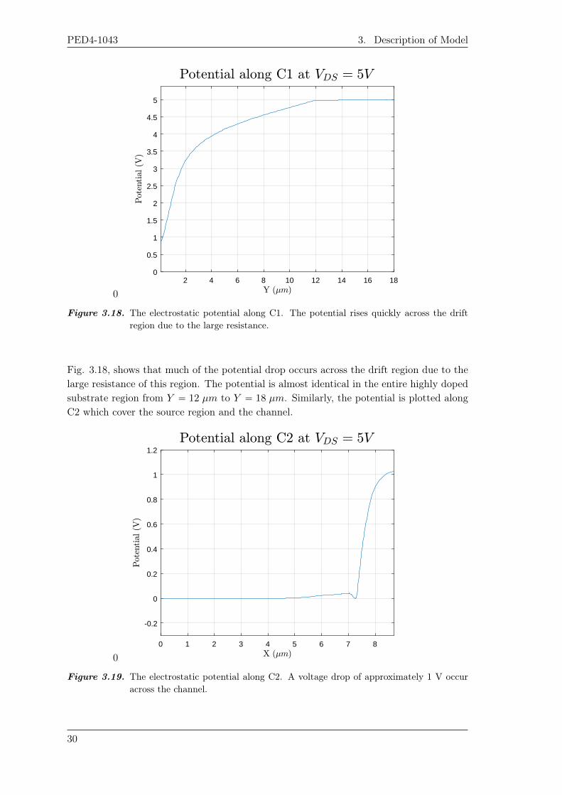
Figure 3.18. The electrostatic potential along C1. The potential rises quickly across the driftregion due to the large resistance.
Fig. 3.18, shows that much of the potential drop occurs across the drift region due to thelarge resistance of this region. The potential is almost identical in the entire highly dopedsubstrate region from Y “ 12 µm to Y “ 18 µm. Similarly, the potential is plotted alongC2 which cover the source region and the channel.
00 1 2 3 4 5 6 7 8
X (7m)
-0.2
0
0.2
0.4
0.6
0.8
1
1.2
Pot
ential
(V)
Potential along C2 at VDS = 5V
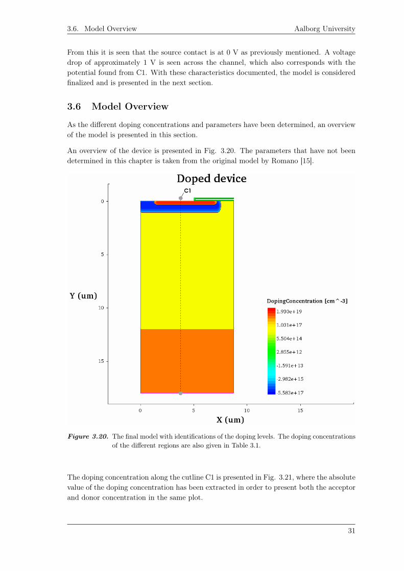
Figure 3.19. The electrostatic potential along C2. A voltage drop of approximately 1 V occuracross the channel.
30
3.6. Model Overview Aalborg University
From this it is seen that the source contact is at 0 V as previously mentioned. A voltagedrop of approximately 1 V is seen across the channel, which also corresponds with thepotential found from C1. With these characteristics documented, the model is consideredfinalized and is presented in the next section.
3.6 Model Overview
As the different doping concentrations and parameters have been determined, an overviewof the model is presented in this section.
An overview of the device is presented in Fig. 3.20. The parameters that have not beendetermined in this chapter is taken from the original model by Romano [15].
Figure 3.20. The final model with identifications of the doping levels. The doping concentrationsof the different regions are also given in Table 3.1.
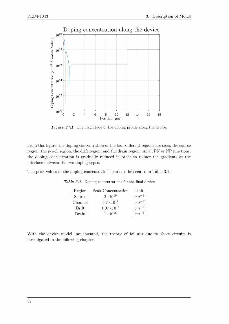
The doping concentration along the cutline C1 is presented in Fig. 3.21, where the absolutevalue of the doping concentration has been extracted in order to present both the acceptorand donor concentration in the same plot.
31
PED4-1043 3. Description of Model
0 2 4 6 8 10 12 14 16 18Position (7m)
1010
1012
1014
1016
1018
1020
Dop
ing
Con
centr
atio
n(c
m!
3A
bso
lute
Val
ue)
Doping concentration along the device
Figure 3.21. The magnitude of the doping profile along the device.
From this figure, the doping concentration of the four different regions are seen; the sourceregion, the p-well region, the drift region, and the drain region. At all PN or NP junctions,the doping concentration is gradually reduced in order to reduce the gradients at theinterface between the two doping types.
The peak values of the doping concentrations can also be seen from Table 3.1.
Table 3.1. Doping concentrations for the final device
Region Peak Concentration UnitSource 2 ¨ 1019 [cm´3]Channel 5.7 ¨ 1017 [cm´3]Drift 1.07 ¨ 1016 [cm´3]Drain 1 ¨ 1018 [cm´3]
With the device model implemented, the theory of failures due to short circuits isinvestigated in the following chapter.
32
Short Circuit Capability ofSiC MOSFETs 4
One of the major reliability concerns of high power modules is the capability of withstandingan externally applied short-circuit, the so-called short-circuit capability. In this section, thedifferent failure mechanism due to short circuit will be explained.
4.1 Description of Short-Circuit Behavior
During a short-circuit, high voltage and high current is simultaneous applied to the device,hence a high power is dissipated in the device. This may occur if two devices in the sameinverter leg is turned on simultaneous, for example due to the failure of a gate driver, ora second turn-on because of induced EMI. This high power is applied until the gate driverhas detected the failure and the device is turned off. Often this time is in the order of 10µs, as this is a usual short-circuit withstand time of a conventional Si IGBT [20].
The power applied to the device is determined by the applied voltage across the device,and the characteristics of the device in its saturation region. The dissipated energy can befound by the integral of this power [2].
Esc “
ż tsc
0VDSpτq ¨ IDpτq dτ (4.1)
Where VDS is the voltage across the device, ID is the drain current, tsc is the time periodbefore the device is turned off, and τ is an integration variable.The energy dissipated in the device will result in an increased temperature. This increasedtemperature can cause a so-called thermal runaway. In this failure mode, the device doesnot fail immediately at the time of the short-circuit. Instead an increased leakage currentis seen after the shut-off of the device due to the higher internal temperature of the device.Because of the combination of a high blocking voltage and an increased current, a highamount of power is generated in the device despite the fact that the short-circuit conditionsare no longer present. If this power is higher than the power transfered away from thehot-spot, the temperature will increase even further. This will results in an even biggerleakage current, creating a positive feedback mechanism that leads to a thermal runaway.
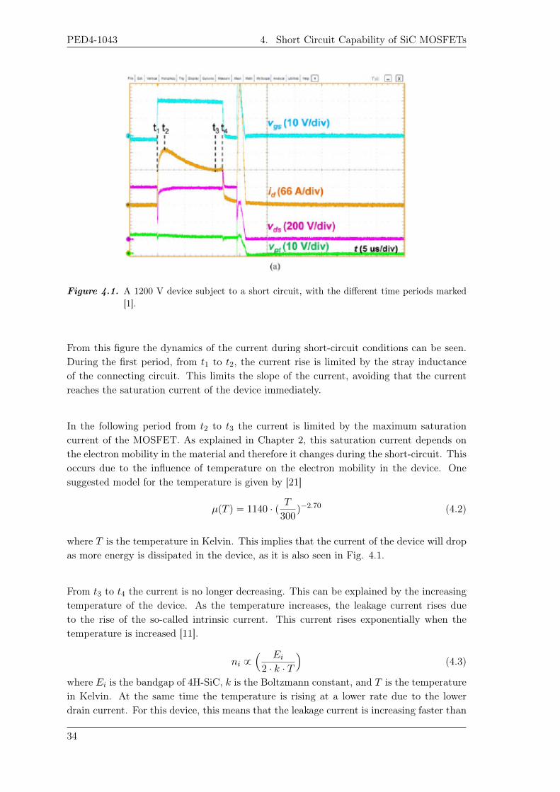
Wang et al. [1], the so-called Short-Circuit Withstand Time (SCWT) was investigated.It was investigated how long time a 1200 V device from Cree can sustain short-circuitconditions. One of these short-circuit tests is shown in Fig. 4.1.
33
PED4-1043 4. Short Circuit Capability of SiC MOSFETs
Figure 4.1. A 1200 V device subject to a short circuit, with the different time periods marked[1].
From this figure the dynamics of the current during short-circuit conditions can be seen.During the first period, from t1 to t2, the current rise is limited by the stray inductanceof the connecting circuit. This limits the slope of the current, avoiding that the currentreaches the saturation current of the device immediately.
In the following period from t2 to t3 the current is limited by the maximum saturationcurrent of the MOSFET. As explained in Chapter 2, this saturation current depends onthe electron mobility in the material and therefore it changes during the short-circuit. Thisoccurs due to the influence of temperature on the electron mobility in the device. Onesuggested model for the temperature is given by [21]
µpT q “ 1140 ¨ pT
300q´2.70 (4.2)
where T is the temperature in Kelvin. This implies that the current of the device will dropas more energy is dissipated in the device, as it is also seen in Fig. 4.1.
From t3 to t4 the current is no longer decreasing. This can be explained by the increasingtemperature of the device. As the temperature increases, the leakage current rises dueto the rise of the so-called intrinsic current. This current rises exponentially when thetemperature is increased [11].
ni 9´ Ei
2 ¨ k ¨ T
¯
(4.3)
where Ei is the bandgap of 4H-SiC, k is the Boltzmann constant, and T is the temperaturein Kelvin. At the same time the temperature is rising at a lower rate due to the lowerdrain current. For this device, this means that the leakage current is increasing faster than
34
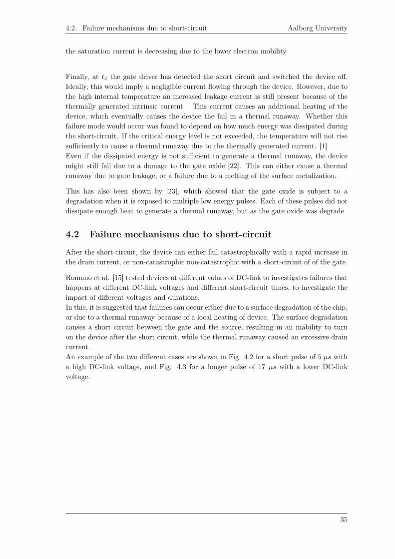
4.2. Failure mechanisms due to short-circuit Aalborg University
the saturation current is decreasing due to the lower electron mobility.
Finally, at t4 the gate driver has detected the short circuit and switched the device off.Ideally, this would imply a negligible current flowing through the device. However, due tothe high internal temperature an increased leakage current is still present because of thethermally generated intrinsic current . This current causes an additional heating of thedevice, which eventually causes the device the fail in a thermal runaway. Whether thisfailure mode would occur was found to depend on how much energy was dissipated duringthe short-circuit. If the critical energy level is not exceeded, the temperature will not risesufficiently to cause a thermal runaway due to the thermally generated current. [1]Even if the dissipated energy is not sufficient to generate a thermal runaway, the devicemight still fail due to a damage to the gate oxide [22]. This can either cause a thermalrunaway due to gate leakage, or a failure due to a melting of the surface metalization.
This has also been shown by [23], which showed that the gate oxide is subject to adegradation when it is exposed to multiple low energy pulses. Each of these pulses did notdissipate enough heat to generate a thermal runaway, but as the gate oxide was degrade
4.2 Failure mechanisms due to short-circuit
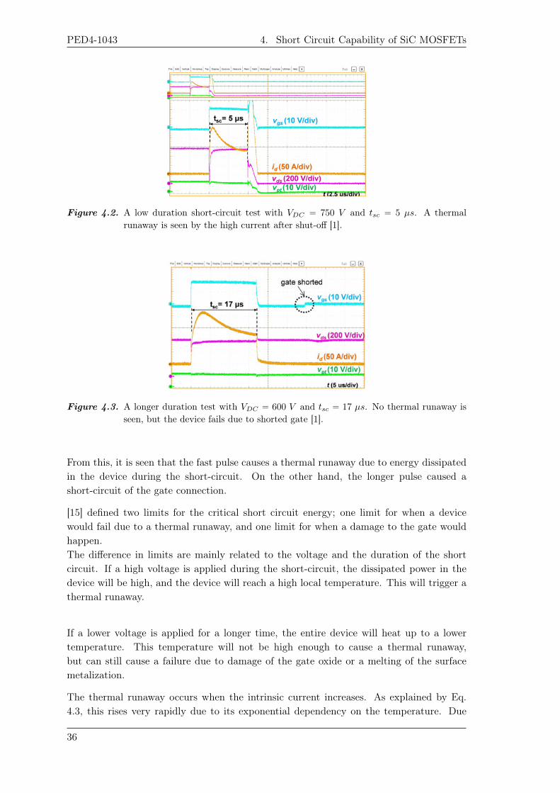
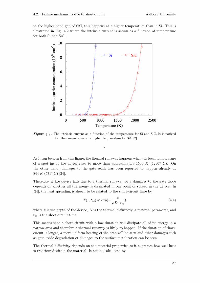
After the short-circuit, the device can either fail catastrophically with a rapid increase inthe drain current, or non-catastrophic non-catastrophic with a short-circuit of of the gate.
Romano et al. [15] tested devices at different values of DC-link to investigates failures thathappens at different DC-link voltages and different short-circuit times, to investigate theimpact of different voltages and durations.In this, it is suggested that failures can occur either due to a surface degradation of the chip,or due to a thermal runaway because of a local heating of device. The surface degradationcauses a short circuit between the gate and the source, resulting in an inability to turnon the device after the short circuit, while the thermal runaway caused an excessive draincurrent.An example of the two different cases are shown in Fig. 4.2 for a short pulse of 5 µs witha high DC-link voltage, and Fig. 4.3 for a longer pulse of 17 µs with a lower DC-linkvoltage.
35
PED4-1043 4. Short Circuit Capability of SiC MOSFETs
Figure 4.2. A low duration short-circuit test with VDC “ 750 V and tsc “ 5 µs. A thermalrunaway is seen by the high current after shut-off [1].
Figure 4.3. A longer duration test with VDC “ 600 V and tsc “ 17 µs. No thermal runaway isseen, but the device fails due to shorted gate [1].
From this, it is seen that the fast pulse causes a thermal runaway due to energy dissipatedin the device during the short-circuit. On the other hand, the longer pulse caused ashort-circuit of the gate connection.
[15] defined two limits for the critical short circuit energy; one limit for when a devicewould fail due to a thermal runaway, and one limit for when a damage to the gate wouldhappen.The difference in limits are mainly related to the voltage and the duration of the shortcircuit. If a high voltage is applied during the short-circuit, the dissipated power in thedevice will be high, and the device will reach a high local temperature. This will trigger athermal runaway.
If a lower voltage is applied for a longer time, the entire device will heat up to a lowertemperature. This temperature will not be high enough to cause a thermal runaway,but can still cause a failure due to damage of the gate oxide or a melting of the surfacemetalization.
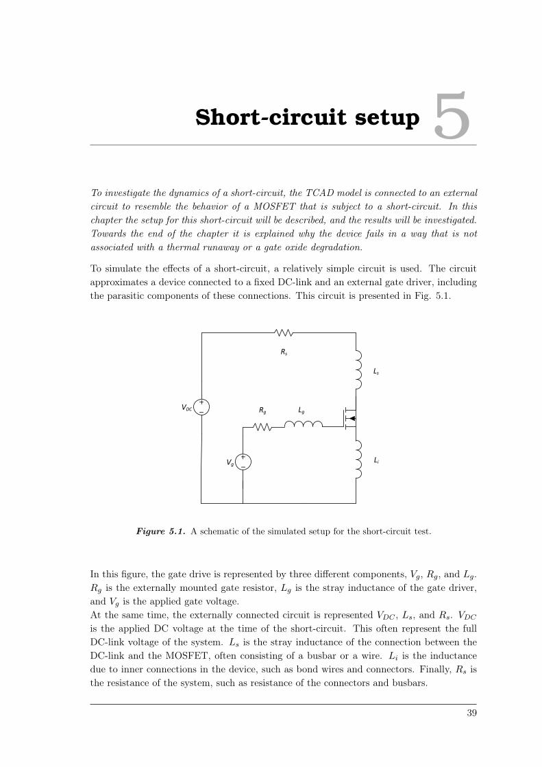
The thermal runaway occurs when the intrinsic current increases. As explained by Eq.4.3, this rises very rapidly due to its exponential dependency on the temperature. Due
36
4.2. Failure mechanisms due to short-circuit Aalborg University
to the higher band gap of SiC, this happens at a higher temperature than in Si. This isillustrated in Fig. 4.2 where the intrinsic current is shown as a function of temperaturefor both Si and SiC.
Figure 4.4. The intrinsic current as a function of the temperature for Si and SiC. It is noticedthat the current rises at a higher temperature for SiC [2].
.
As it can be seen from this figure, the thermal runaway happens when the local temperatureof a spot inside the device rises to more than approximately 1500 K p1230˝ Cq. Onthe other hand, damages to the gate oxide has been reported to happen already at844 K p571˝ Cq [24].
Therefore, if the device fails due to a thermal runaway or a damages to the gate oxidedepends on whether all the energy is dissipated in one point or spread in the device. In[24], the heat spreading is shown to be related to the short-circuit time by
T pz, tscq 9 expp´z
?D ¨ tsc
q (4.4)
where z is the depth of the device, D is the thermal diffusivity, a material parameter, andtsc is the short-circuit time.
This means that a short circuit with a low duration will dissipate all of its energy in anarrow area and therefore a thermal runaway is likely to happen. If the duration of short-circuit is longer, a more uniform heating of the area will be seen and other damages suchas gate oxide degradation or damages to the surface metalization can be seen.
The thermal diffusivity depends on the material properties as it expresses how well heatis transferred within the material. It can be calculated by
37

PED4-1043 4. Short Circuit Capability of SiC MOSFETs
D “k
ρ ¨ cp(4.5)
where k is the thermal conductivity, ρ is the density and cp is the specific heat capacity.The thermal parameters of 4H-SiC are given in Tab. 4.1.
Table 4.1. Thermal properties for 4H-SiC [2].
Property Unit ValueDensity [gcm3] 3.21
Specific Heat Capacity [Jpg ¨Kq] 0.6736Thermal Conductivity [W pcm ¨Kq] 4.5
Using this knowledge, it is desired to use the derived model to test a short-circuit atdifferent voltages, to understand the inner failure mechanism. Furthermore, it is desiredto check at which voltages the local heating is enough to cause a thermal runaway andat which voltages the short circuit causes a more uniform heating which may damage thegate oxide.
38
Short-circuit setup 5To investigate the dynamics of a short-circuit, the TCAD model is connected to an externalcircuit to resemble the behavior of a MOSFET that is subject to a short-circuit. In thischapter the setup for this short-circuit will be described, and the results will be investigated.Towards the end of the chapter it is explained why the device fails in a way that is notassociated with a thermal runaway or a gate oxide degradation.
To simulate the effects of a short-circuit, a relatively simple circuit is used. The circuitapproximates a device connected to a fixed DC-link and an external gate driver, includingthe parasitic components of these connections. This circuit is presented in Fig. 5.1.
VDC
Vg
Ls
LgRg
Rs
Li
Figure 5.1. A schematic of the simulated setup for the short-circuit test.
In this figure, the gate drive is represented by three different components, Vg, Rg, and Lg.Rg is the externally mounted gate resistor, Lg is the stray inductance of the gate driver,and Vg is the applied gate voltage.At the same time, the externally connected circuit is represented VDC , Ls, and Rs. VDC
is the applied DC voltage at the time of the short-circuit. This often represent the fullDC-link voltage of the system. Ls is the stray inductance of the connection between theDC-link and the MOSFET, often consisting of a busbar or a wire. Li is the inductancedue to inner connections in the device, such as bond wires and connectors. Finally, Rs isthe resistance of the system, such as resistance of the connectors and busbars.
39

PED4-1043 5. Short-circuit setup
Table 5.1. Parameters for the short-circuit test shown in Fig 5.1.
Symbol Parameter Value UnitVg Gate Voltage ´520 [V ]Rg Gate Resistor 10 [Ω]Lg Gate Inductance 40 [nH]VDC DC-Voltage 800 [V ]Ls Circuit Inductance 100 [nH]Rs Stray Resistance 1 [mΩ]Li Stray Inductance 10 [nH]
For this project, a so-called Hard Switching Failure, HSF, is considered. This happenswhen the device is switched on while the full DC-link voltage is still applied. This can forinstance happen if the other MOSFET of the phase leg in an inverter fails to turn off, andthereby is not blocking any voltage.
5.1 Simulation of Short-circuit
At first, a low voltage short-circuit is performed to test the setup of the short-circuits. Thistest is performed at VDC “ 100 V . To improve convergence the thermodynamic effects areneglected.
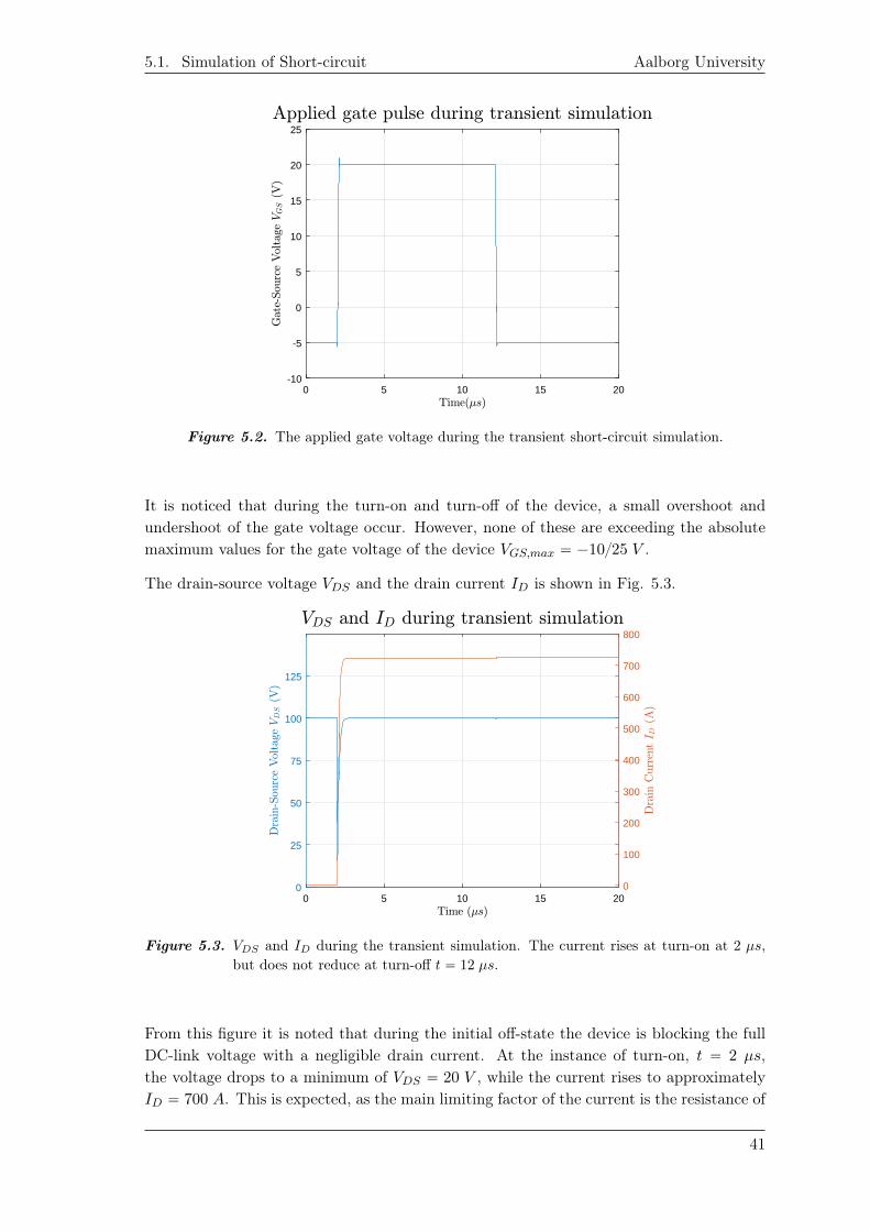
At first the simulated DC-link voltage is ramped up by applying a quasi-stationarysimulation with an increased voltage. A slew rate of one volt per second is used to ensurethat no excessive in-rush current is occurring. At the same a gate voltage of VGS “ ´5 V isapplied that the device is fully off. Afterwards, a transient analysis is performed using theinitial conditions established during the quasi-stationary simulation. In this simulation,the gate voltage is kept at ´5 V for 2 µs. After this period the gate supply voltage ischanged from ´5 V to 20 V during a time period of 0.1 µs. A gate resistance of 10Ω isused. Finally, the device is turned off after 8 µs by applying a negative gate voltage of´5 V . The total gate pulse is shown in Fig. 5.2.
40
5.1. Simulation of Short-circuit Aalborg University
0 5 10 15 20Time(7s)
-10
-5
0
5
10
15
20
25
Gat
e-Sou
rce
Vol
tage
VG
S(V
)
Applied gate pulse during transient simulation
Figure 5.2. The applied gate voltage during the transient short-circuit simulation.
It is noticed that during the turn-on and turn-off of the device, a small overshoot andundershoot of the gate voltage occur. However, none of these are exceeding the absolutemaximum values for the gate voltage of the device VGS,max “ ´1025 V .
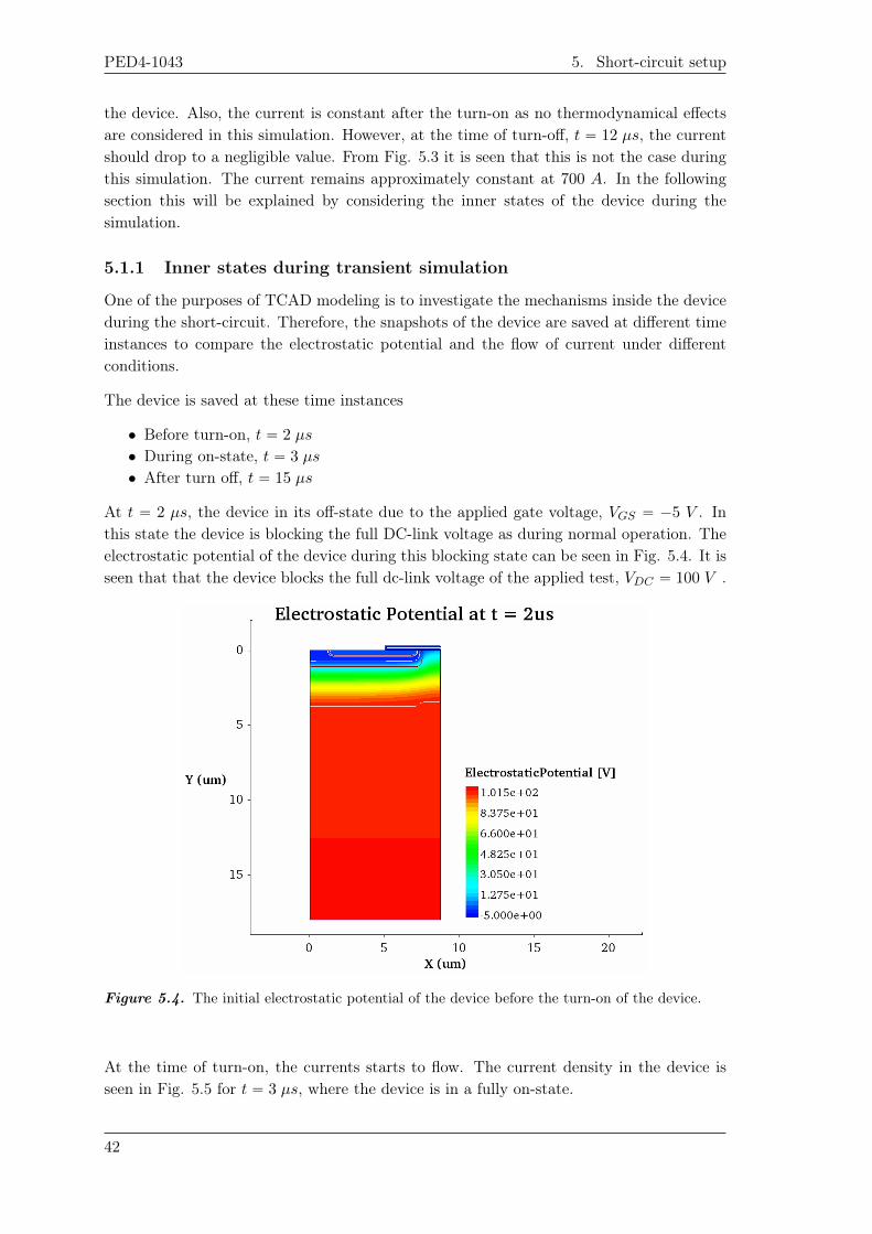
The drain-source voltage VDS and the drain current ID is shown in Fig. 5.3.
0 5 10 15 20Time (7s)
0
25
50
75
100
125
Dra
in-S
ourc
eVol
tage
VD
S(V
)
VDS and ID during transient simulation
0
100
200
300
400
500
600
700
800D
rain
Curr
entI D
(A)
Figure 5.3. VDS and ID during the transient simulation. The current rises at turn-on at 2 µs,but does not reduce at turn-off t “ 12 µs.
From this figure it is noted that during the initial off-state the device is blocking the fullDC-link voltage with a negligible drain current. At the instance of turn-on, t “ 2 µs,the voltage drops to a minimum of VDS “ 20 V , while the current rises to approximatelyID “ 700 A. This is expected, as the main limiting factor of the current is the resistance of
41
PED4-1043 5. Short-circuit setup
the device. Also, the current is constant after the turn-on as no thermodynamical effectsare considered in this simulation. However, at the time of turn-off, t “ 12 µs, the currentshould drop to a negligible value. From Fig. 5.3 it is seen that this is not the case duringthis simulation. The current remains approximately constant at 700 A. In the followingsection this will be explained by considering the inner states of the device during thesimulation.
5.1.1 Inner states during transient simulation
One of the purposes of TCAD modeling is to investigate the mechanisms inside the deviceduring the short-circuit. Therefore, the snapshots of the device are saved at different timeinstances to compare the electrostatic potential and the flow of current under differentconditions.
The device is saved at these time instances
• Before turn-on, t “ 2 µs
• During on-state, t “ 3 µs
• After turn off, t “ 15 µs
At t “ 2 µs, the device in its off-state due to the applied gate voltage, VGS “ ´5 V . Inthis state the device is blocking the full DC-link voltage as during normal operation. Theelectrostatic potential of the device during this blocking state can be seen in Fig. 5.4. It isseen that that the device blocks the full dc-link voltage of the applied test, VDC “ 100 V .
Figure 5.4. The initial electrostatic potential of the device before the turn-on of the device.
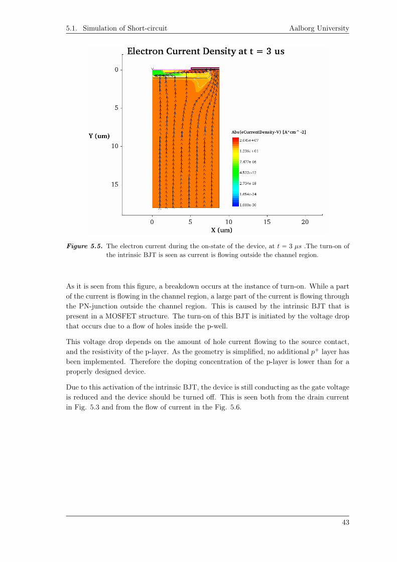
At the time of turn-on, the currents starts to flow. The current density in the device isseen in Fig. 5.5 for t “ 3 µs, where the device is in a fully on-state.
42
5.1. Simulation of Short-circuit Aalborg University
Figure 5.5. The electron current during the on-state of the device, at t “ 3 µs .The turn-on ofthe intrinsic BJT is seen as current is flowing outside the channel region.
As it is seen from this figure, a breakdown occurs at the instance of turn-on. While a partof the current is flowing in the channel region, a large part of the current is flowing throughthe PN-junction outside the channel region. This is caused by the intrinsic BJT that ispresent in a MOSFET structure. The turn-on of this BJT is initiated by the voltage dropthat occurs due to a flow of holes inside the p-well.
This voltage drop depends on the amount of hole current flowing to the source contact,and the resistivity of the p-layer. As the geometry is simplified, no additional p` layer hasbeen implemented. Therefore the doping concentration of the p-layer is lower than for aproperly designed device.
Due to this activation of the intrinsic BJT, the device is still conducting as the gate voltageis reduced and the device should be turned off. This is seen both from the drain currentin Fig. 5.3 and from the flow of current in the Fig. 5.6.
43

PED4-1043 5. Short-circuit setup
Figure 5.6. The current flow after the turn-off of the device. The device is still conducting dueto the turn-on of the intrinsic BJT.
It is noted that the channel is fully off and no current is flowing through this. Therefore,the device should not conduct any current. This is also confirmed from the figure, as allcurrent is flowing through the PN-junction due to the turn-on of the intrinsic BJT.
5.1.2 Activation of the Intrinsic BJT
The turn-on of the intrinsic BJT is caused by the excessive dv/dt that occurs at the devicewhen the device is turned-on while the full blocking voltage is applied. During turn-on, ahole current is flowing in the p-well due to the change of the depletion layer width at thePN-junction. Because of the resistance of the p-well, this causes a voltage drop along thelayer, as illustrated in Fig. 5.7 [11].
44
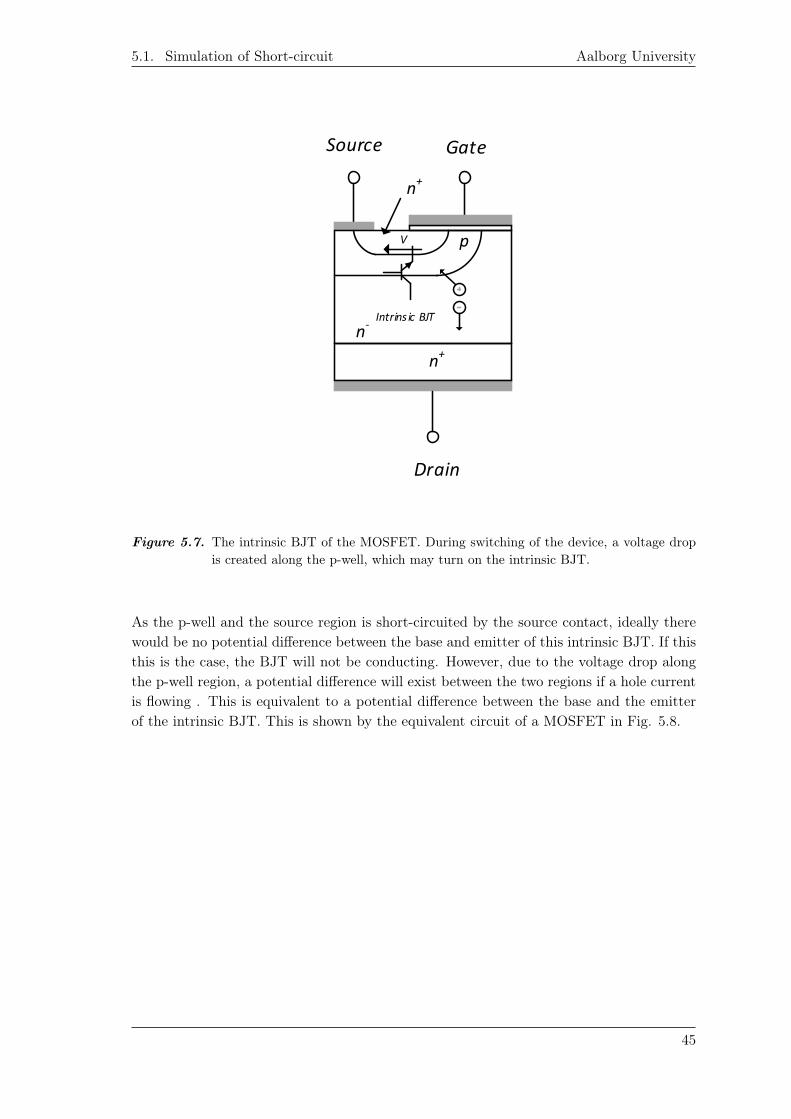
5.1. Simulation of Short-circuit Aalborg University
n-
n+
Source Gate
Drain
V
Intrins ic BJT
p
n+
Figure 5.7. The intrinsic BJT of the MOSFET. During switching of the device, a voltage dropis created along the p-well, which may turn on the intrinsic BJT.
As the p-well and the source region is short-circuited by the source contact, ideally therewould be no potential difference between the base and emitter of this intrinsic BJT. If thisthis is the case, the BJT will not be conducting. However, due to the voltage drop alongthe p-well region, a potential difference will exist between the two regions if a hole currentis flowing . This is equivalent to a potential difference between the base and the emitterof the intrinsic BJT. This is shown by the equivalent circuit of a MOSFET in Fig. 5.8.
45
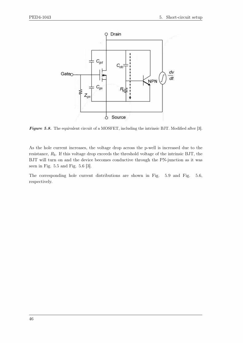
PED4-1043 5. Short-circuit setup
Figure 5.8. The equivalent circuit of a MOSFET, including the intrinsic BJT. Modified after [3].
As the hole current increases, the voltage drop across the p-well is increased due to theresistance, Rb. If this voltage drop exceeds the threshold voltage of the intrinsic BJT, theBJT will turn on and the device becomes conductive through the PN-junction as it wasseen in Fig. 5.5 and Fig. 5.6 [3].
The corresponding hole current distributions are shown in Fig. 5.9 and Fig. 5.6,respectively.
46
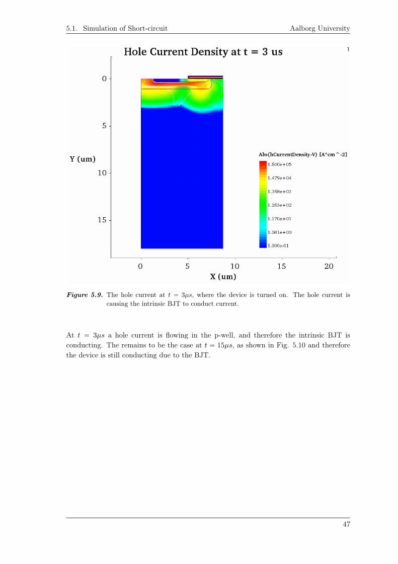
5.1. Simulation of Short-circuit Aalborg University
Figure 5.9. The hole current at t “ 3µs, where the device is turned on. The hole current iscausing the intrinsic BJT to conduct current.
At t “ 3µs a hole current is flowing in the p-well, and therefore the intrinsic BJT isconducting. The remains to be the case at t “ 15µs, as shown in Fig. 5.10 and thereforethe device is still conducting due to the BJT.
47
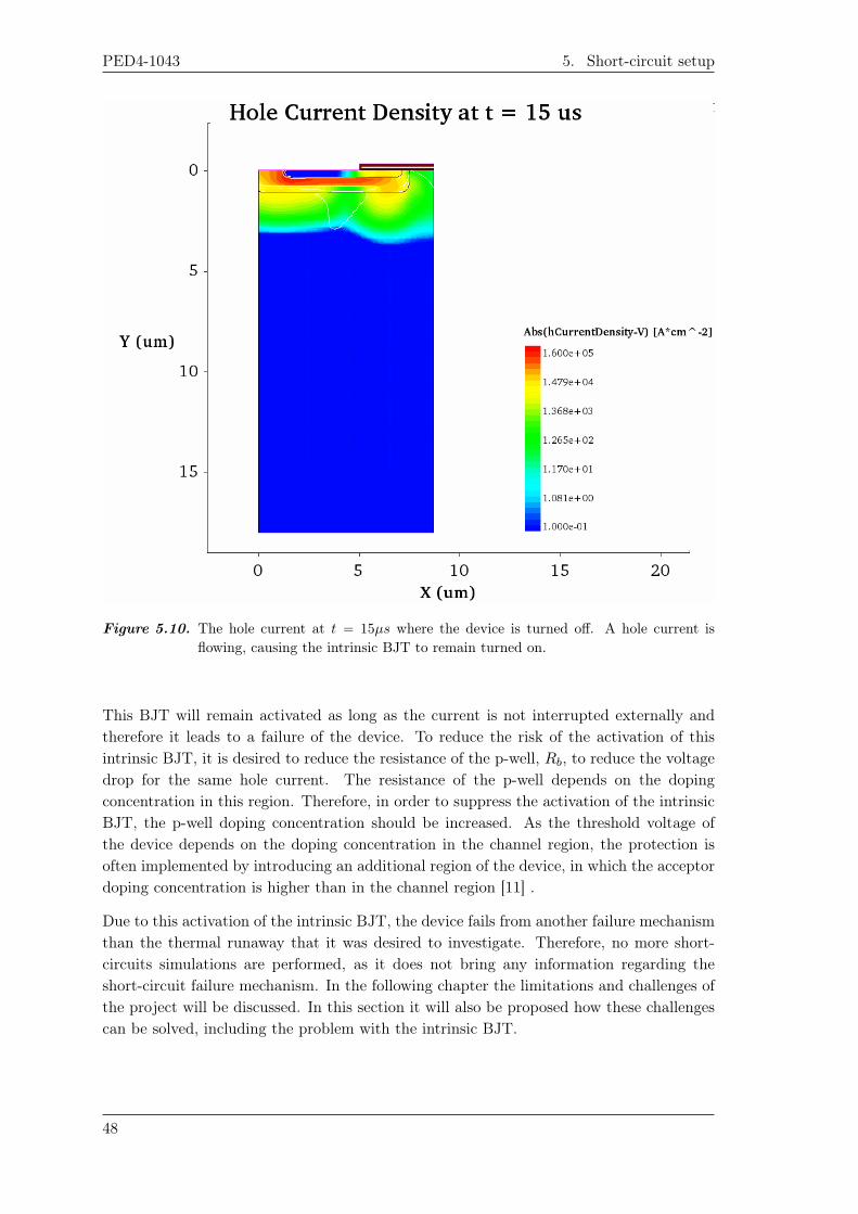
PED4-1043 5. Short-circuit setup
Figure 5.10. The hole current at t “ 15µs where the device is turned off. A hole current isflowing, causing the intrinsic BJT to remain turned on.
This BJT will remain activated as long as the current is not interrupted externally andtherefore it leads to a failure of the device. To reduce the risk of the activation of thisintrinsic BJT, it is desired to reduce the resistance of the p-well, Rb, to reduce the voltagedrop for the same hole current. The resistance of the p-well depends on the dopingconcentration in this region. Therefore, in order to suppress the activation of the intrinsicBJT, the p-well doping concentration should be increased. As the threshold voltage ofthe device depends on the doping concentration in the channel region, the protection isoften implemented by introducing an additional region of the device, in which the acceptordoping concentration is higher than in the channel region [11] .
Due to this activation of the intrinsic BJT, the device fails from another failure mechanismthan the thermal runaway that it was desired to investigate. Therefore, no more short-circuits simulations are performed, as it does not bring any information regarding theshort-circuit failure mechanism. In the following chapter the limitations and challenges ofthe project will be discussed. In this section it will also be proposed how these challengescan be solved, including the problem with the intrinsic BJT.
48
Discussion and FutureWork 6
In this project a number of limitations and difficulties have been described. Many ofthese limitation have a severe impact on the accuracy of the model. While some of theselimitations arise due to limited knowledge of properties of the actual device, others can beavoided by increasing the number of parameters to be determined during the fitting of themodel.
First of all, the influence of the device interface traps was neglected due to the complexityof obtaining the the correct distribution of defects, as multiple types of defects exist.However, as presented in Section 3.4 it has been shown by [19] that the majority of thetraps occurring in the interface is of the acceptor type. Using this knowledge, it might bepossible to increase the accuracy of the model by being only specifying this type of traps.In Sentaurus [25] , it is possible to specify both the concentration and the type of traps.This could be used for achieving better static characteristics of the device, without addingan overwhelming amount of variables to the model due to the many types of interfacetraps.
Another simplification of the model that leads to erroneous results is the uniform dopingconcentration of the p-well. To simplify the implementation of the model, no additionalp` shielding layer was implemented. As it was seen from the results of the short-circuitsimulations in Chapter 5, the lack of this layer causes the device to be prone to an activationof the internal BJT. Therefore, this layer should be implemented to allow the transientbehavior of the device to be simulated. However, as the threshold voltage depends onthe doping concentration in the channel region, the doping concentration should remainunchanged in this region while it is raised in the rest of the p-well.
The final limitation is that the model was made by adjusting the doping concentrationand geometry to resemble the characteristics given in the datasheet. As the datasheet onlyprovide operational values for normal operation, this approach cannot be used comparisonof the model during abnormal conditions, such as short-circuits. Therefore, a natural nextstep would be to compare the behavior of the modelled device with measurements of adevice during these abnormal conditions.
During this project, another type of problems has been encountered: Due to the materialproperties of 4H-SiC, the numerical simulations of a SiC can be challenging [8]. One ofthe major problems in simulation of SiC MOSFETs is the very low intrinsic current ofthe device, which results in very low leakage currents during blocking voltage simulations[18]. This requires higher accuracy representation of the floating points, resulting in an
49
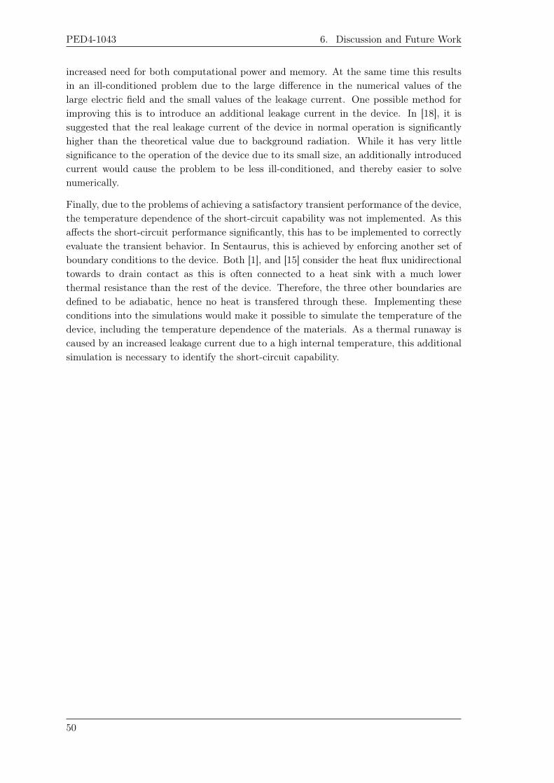
PED4-1043 6. Discussion and Future Work
increased need for both computational power and memory. At the same time this resultsin an ill-conditioned problem due to the large difference in the numerical values of thelarge electric field and the small values of the leakage current. One possible method forimproving this is to introduce an additional leakage current in the device. In [18], it issuggested that the real leakage current of the device in normal operation is significantlyhigher than the theoretical value due to background radiation. While it has very littlesignificance to the operation of the device due to its small size, an additionally introducedcurrent would cause the problem to be less ill-conditioned, and thereby easier to solvenumerically.
Finally, due to the problems of achieving a satisfactory transient performance of the device,the temperature dependence of the short-circuit capability was not implemented. As thisaffects the short-circuit performance significantly, this has to be implemented to correctlyevaluate the transient behavior. In Sentaurus, this is achieved by enforcing another set ofboundary conditions to the device. Both [1], and [15] consider the heat flux unidirectionaltowards to drain contact as this is often connected to a heat sink with a much lowerthermal resistance than the rest of the device. Therefore, the three other boundaries aredefined to be adiabatic, hence no heat is transfered through these. Implementing theseconditions into the simulations would make it possible to simulate the temperature of thedevice, including the temperature dependence of the materials. As a thermal runaway iscaused by an increased leakage current due to a high internal temperature, this additionalsimulation is necessary to identify the short-circuit capability.
50
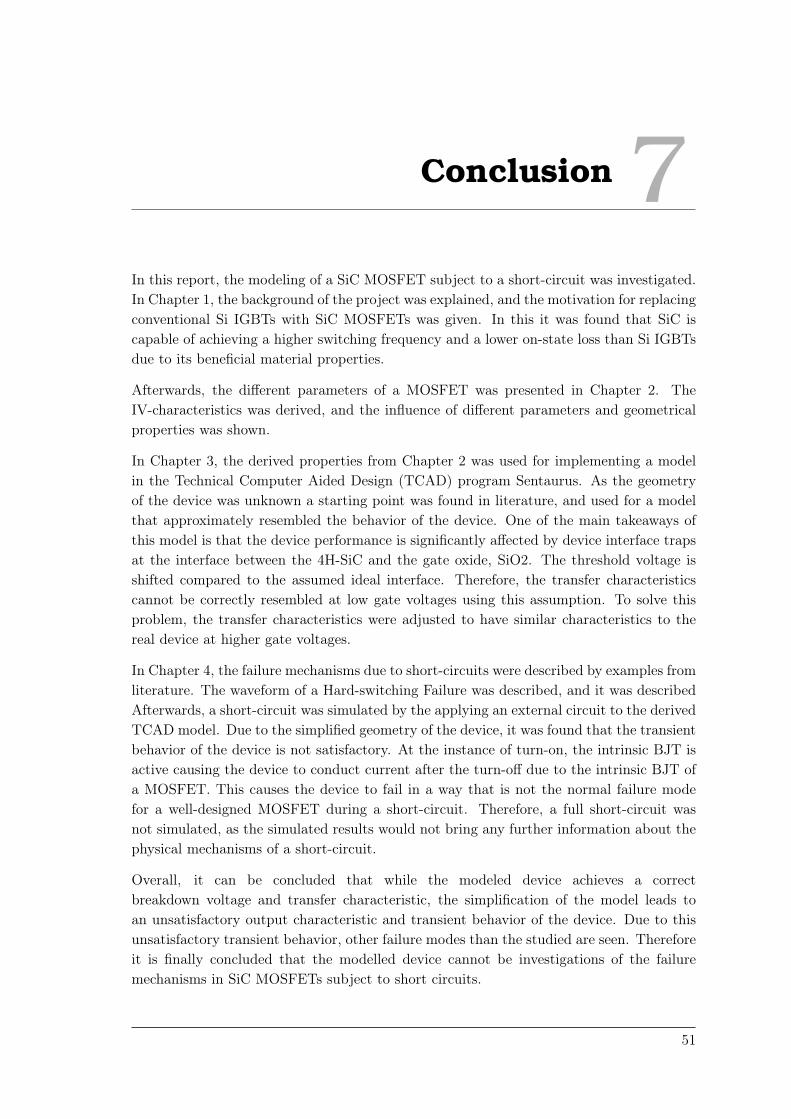
Conclusion 7In this report, the modeling of a SiC MOSFET subject to a short-circuit was investigated.In Chapter 1, the background of the project was explained, and the motivation for replacingconventional Si IGBTs with SiC MOSFETs was given. In this it was found that SiC iscapable of achieving a higher switching frequency and a lower on-state loss than Si IGBTsdue to its beneficial material properties.
Afterwards, the different parameters of a MOSFET was presented in Chapter 2. TheIV-characteristics was derived, and the influence of different parameters and geometricalproperties was shown.
In Chapter 3, the derived properties from Chapter 2 was used for implementing a modelin the Technical Computer Aided Design (TCAD) program Sentaurus. As the geometryof the device was unknown a starting point was found in literature, and used for a modelthat approximately resembled the behavior of the device. One of the main takeaways ofthis model is that the device performance is significantly affected by device interface trapsat the interface between the 4H-SiC and the gate oxide, SiO2. The threshold voltage isshifted compared to the assumed ideal interface. Therefore, the transfer characteristicscannot be correctly resembled at low gate voltages using this assumption. To solve thisproblem, the transfer characteristics were adjusted to have similar characteristics to thereal device at higher gate voltages.
In Chapter 4, the failure mechanisms due to short-circuits were described by examples fromliterature. The waveform of a Hard-switching Failure was described, and it was describedAfterwards, a short-circuit was simulated by the applying an external circuit to the derivedTCAD model. Due to the simplified geometry of the device, it was found that the transientbehavior of the device is not satisfactory. At the instance of turn-on, the intrinsic BJT isactive causing the device to conduct current after the turn-off due to the intrinsic BJT ofa MOSFET. This causes the device to fail in a way that is not the normal failure modefor a well-designed MOSFET during a short-circuit. Therefore, a full short-circuit wasnot simulated, as the simulated results would not bring any further information about thephysical mechanisms of a short-circuit.
Overall, it can be concluded that while the modeled device achieves a correctbreakdown voltage and transfer characteristic, the simplification of the model leads toan unsatisfactory output characteristic and transient behavior of the device. Due to thisunsatisfactory transient behavior, other failure modes than the studied are seen. Thereforeit is finally concluded that the modelled device cannot be investigations of the failuremechanisms in SiC MOSFETs subject to short circuits.
51

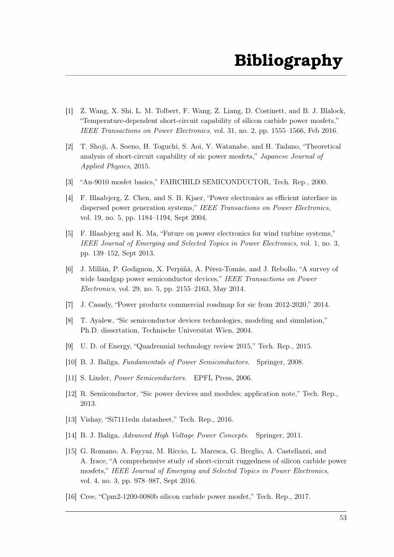
Bibliography
[1] Z. Wang, X. Shi, L. M. Tolbert, F. Wang, Z. Liang, D. Costinett, and B. J. Blalock,“Temperature-dependent short-circuit capability of silicon carbide power mosfets,”IEEE Transactions on Power Electronics, vol. 31, no. 2, pp. 1555–1566, Feb 2016.
[2] T. Shoji, A. Soeno, H. Toguchi, S. Aoi, Y. Watanabe, and H. Tadano, “Theoreticalanalysis of short-circuit capability of sic power mosfets,” Japanese Journal ofApplied Physics, 2015.
[3] “An-9010 mosfet basics,” FAIRCHILD SEMICONDUCTOR, Tech. Rep., 2000.
[4] F. Blaabjerg, Z. Chen, and S. B. Kjaer, “Power electronics as efficient interface indispersed power generation systems,” IEEE Transactions on Power Electronics,vol. 19, no. 5, pp. 1184–1194, Sept 2004.
[5] F. Blaabjerg and K. Ma, “Future on power electronics for wind turbine systems,”IEEE Journal of Emerging and Selected Topics in Power Electronics, vol. 1, no. 3,pp. 139–152, Sept 2013.
[6] J. Millán, P. Godignon, X. Perpiñà, A. Pérez-Tomás, and J. Rebollo, “A survey ofwide bandgap power semiconductor devices,” IEEE Transactions on PowerElectronics, vol. 29, no. 5, pp. 2155–2163, May 2014.
[7] J. Casady, “Power products commercial roadmap for sic from 2012-2020,” 2014.
[8] T. Ayalew, “Sic semiconductor devices technologies, modeling and simulation,”Ph.D. dissertation, Technische Universitat Wien, 2004.
[9] U. D. of Energy, “Quadrennial technology review 2015,” Tech. Rep., 2015.
[10] B. J. Baliga, Fundamentals of Power Semiconductors. Springer, 2008.
[11] S. Linder, Power Semiconductors. EPFL Press, 2006.
[12] R. Semiconductor, “Sic power devices and modules; application note,” Tech. Rep.,2013.
[13] Vishay, “Si7111edn datasheet,” Tech. Rep., 2016.
[14] B. J. Baliga, Advanced High Voltage Power Concepts. Springer, 2011.
[15] G. Romano, A. Fayyaz, M. Riccio, L. Maresca, G. Breglio, A. Castellazzi, andA. Irace, “A comprehensive study of short-circuit ruggedness of silicon carbide powermosfets,” IEEE Journal of Emerging and Selected Topics in Power Electronics,vol. 4, no. 3, pp. 978–987, Sept 2016.
[16] Cree, “Cpm2-1200-0080b silicon carbide power mosfet,” Tech. Rep., 2017.
53
PED4-1043 Bibliography
[17] R. Wolfson, Essential University Physics. Pearson, 2013.
[18] Device Simulation of 3D Trench Gate 4H-SiC IGBT Device.
[19] V. Uhnevionak, “Simulation and modeling of silicon-carbide devices,” Ph.D.dissertation, Friedrich-Alexander-Universitat Erlangen-Nurnberg, 2015.
[20] D. P. Sadik, J. Colmenares, G. Tolstoy, D. Peftitsis, M. Bakowski, J. Rabkowski,and H. P. Nee, “Short-circuit protection circuits for silicon-carbide powertransistors,” IEEE Transactions on Industrial Electronics, vol. 63, no. 4, pp.1995–2004, April 2016.
[21] J. Baliga, Silicon Carbide Power Devices, 2005.
[22] P. D. Reigosa, F. Iannuzzo, H. Luo, and F. Blaabjerg, “A short circuit safe operationarea identification criterion for sic mosfet power modules,” IEEE Transactions onIndustry Applications, vol. PP, no. 99, pp. 1–1, 2016.
[23] T. T. Nguyen, A. Ahmed, T. V. Thang, and J. H. Park, “Gate oxide reliability issuesof sic mosfets under short-circuit operation,” IEEE Transactions on PowerElectronics, vol. 30, no. 5, pp. 2445–2455, May 2015.
[24] J. An, M. Namai, and N. Iwamuro, “Experimental and theoretical analyses of gateoxide and junction reliability for 4h-sic mosfet under short-circuit operation,”Japanese Journal of Applied Physics, vol. 55, no. 12, p. 124102, 2016. [Online].Available: http://stacks.iop.org/1347-4065/55/i=12/a=124102
[25] Sentaurus Device Manual.
54