Embed Size (px)
Citation preview
Stellaris® LM3S2601 Microcontroller
DATA SHEET
Copyr ight © 2007-2014Texas Instruments Incorporated
DS-LM3S2601-15852.2743SPMS045I
TEXAS INSTRUMENTS-PRODUCTION DATA

CopyrightCopyright © 2007-2014 Texas Instruments Incorporated All rights reserved. Stellaris and StellarisWare® are registered trademarks of Texas InstrumentsIncorporated. ARM and Thumb are registered trademarks and Cortex is a trademark of ARM Limited. Other names and brands may be claimed as theproperty of others.
PRODUCTION DATA information is current as of publication date. Products conform to specifications per the terms of Texas Instruments standardwarranty. Production processing does not necessarily include testing of all parameters.
Please be aware that an important notice concerning availability, standard warranty, and use in critical applications of Texas Instruments semiconductorproducts and disclaimers thereto appears at the end of this data sheet.
Texas Instruments Incorporated108 Wild Basin, Suite 350Austin, TX 78746http://www.ti.com/stellarishttp://www-k.ext.ti.com/sc/technical-support/product-information-centers.htm
July 16, 20142Texas Instruments-Production Data
Table of ContentsRevision History ............................................................................................................................. 22About This Document .................................................................................................................... 28Audience .............................................................................................................................................. 28About This Manual ................................................................................................................................ 28Related Documents ............................................................................................................................... 28Documentation Conventions .................................................................................................................. 29
1 Architectural Overview .......................................................................................... 311.1 Product Features .......................................................................................................... 311.2 Target Applications ........................................................................................................ 381.3 High-Level Block Diagram ............................................................................................. 381.4 Functional Overview ...................................................................................................... 401.4.1 ARM Cortex™-M3 ......................................................................................................... 401.4.2 Motor Control Peripherals .............................................................................................. 411.4.3 Analog Peripherals ........................................................................................................ 411.4.4 Serial Communications Peripherals ................................................................................ 411.4.5 System Peripherals ....................................................................................................... 431.4.6 Memory Peripherals ...................................................................................................... 441.4.7 Additional Features ....................................................................................................... 441.4.8 Hardware Details .......................................................................................................... 45
2 The Cortex-M3 Processor ...................................................................................... 462.1 Block Diagram .............................................................................................................. 472.2 Overview ...................................................................................................................... 482.2.1 System-Level Interface .................................................................................................. 482.2.2 Integrated Configurable Debug ...................................................................................... 482.2.3 Trace Port Interface Unit (TPIU) ..................................................................................... 492.2.4 Cortex-M3 System Component Details ........................................................................... 492.3 Programming Model ...................................................................................................... 502.3.1 Processor Mode and Privilege Levels for Software Execution ........................................... 502.3.2 Stacks .......................................................................................................................... 502.3.3 Register Map ................................................................................................................ 512.3.4 Register Descriptions .................................................................................................... 522.3.5 Exceptions and Interrupts .............................................................................................. 652.3.6 Data Types ................................................................................................................... 652.4 Memory Model .............................................................................................................. 652.4.1 Memory Regions, Types and Attributes ........................................................................... 672.4.2 Memory System Ordering of Memory Accesses .............................................................. 672.4.3 Behavior of Memory Accesses ....................................................................................... 672.4.4 Software Ordering of Memory Accesses ......................................................................... 682.4.5 Bit-Banding ................................................................................................................... 692.4.6 Data Storage ................................................................................................................ 712.4.7 Synchronization Primitives ............................................................................................. 722.5 Exception Model ........................................................................................................... 732.5.1 Exception States ........................................................................................................... 742.5.2 Exception Types ............................................................................................................ 742.5.3 Exception Handlers ....................................................................................................... 77
3July 16, 2014Texas Instruments-Production Data
Stellaris® LM3S2601 Microcontroller
2.5.4 Vector Table .................................................................................................................. 772.5.5 Exception Priorities ....................................................................................................... 782.5.6 Interrupt Priority Grouping .............................................................................................. 792.5.7 Exception Entry and Return ........................................................................................... 792.6 Fault Handling .............................................................................................................. 812.6.1 Fault Types ................................................................................................................... 822.6.2 Fault Escalation and Hard Faults .................................................................................... 822.6.3 Fault Status Registers and Fault Address Registers ........................................................ 832.6.4 Lockup ......................................................................................................................... 832.7 Power Management ...................................................................................................... 832.7.1 Entering Sleep Modes ................................................................................................... 842.7.2 Wake Up from Sleep Mode ............................................................................................ 842.8 Instruction Set Summary ............................................................................................... 85
3 Cortex-M3 Peripherals ........................................................................................... 883.1 Functional Description ................................................................................................... 883.1.1 System Timer (SysTick) ................................................................................................. 883.1.2 Nested Vectored Interrupt Controller (NVIC) .................................................................... 893.1.3 System Control Block (SCB) .......................................................................................... 913.1.4 Memory Protection Unit (MPU) ....................................................................................... 913.2 Register Map ................................................................................................................ 963.3 System Timer (SysTick) Register Descriptions ................................................................ 983.4 NVIC Register Descriptions .......................................................................................... 1023.5 System Control Block (SCB) Register Descriptions ........................................................ 1153.6 Memory Protection Unit (MPU) Register Descriptions .................................................... 142
4 JTAG Interface ...................................................................................................... 1524.1 Block Diagram ............................................................................................................ 1534.2 Signal Description ....................................................................................................... 1534.3 Functional Description ................................................................................................. 1544.3.1 JTAG Interface Pins ..................................................................................................... 1544.3.2 JTAG TAP Controller ................................................................................................... 1564.3.3 Shift Registers ............................................................................................................ 1574.3.4 Operational Considerations .......................................................................................... 1574.4 Initialization and Configuration ..................................................................................... 1604.5 Register Descriptions .................................................................................................. 1604.5.1 Instruction Register (IR) ............................................................................................... 1604.5.2 Data Registers ............................................................................................................ 163
5 System Control ..................................................................................................... 1655.1 Signal Description ....................................................................................................... 1655.2 Functional Description ................................................................................................. 1655.2.1 Device Identification .................................................................................................... 1665.2.2 Reset Control .............................................................................................................. 1665.2.3 Power Control ............................................................................................................. 1705.2.4 Clock Control .............................................................................................................. 1715.2.5 System Control ........................................................................................................... 1765.3 Initialization and Configuration ..................................................................................... 1775.4 Register Map .............................................................................................................. 1775.5 Register Descriptions .................................................................................................. 179
July 16, 20144Texas Instruments-Production Data
Table of Contents
6 Hibernation Module .............................................................................................. 2316.1 Block Diagram ............................................................................................................ 2326.2 Signal Description ....................................................................................................... 2326.3 Functional Description ................................................................................................. 2336.3.1 Register Access Timing ............................................................................................... 2336.3.2 Clock Source .............................................................................................................. 2346.3.3 Battery Management ................................................................................................... 2356.3.4 Real-Time Clock .......................................................................................................... 2356.3.5 Battery-Backed Memory .............................................................................................. 2366.3.6 Power Control ............................................................................................................. 2366.3.7 Initiating Hibernate ...................................................................................................... 2366.3.8 Interrupts and Status ................................................................................................... 2376.4 Initialization and Configuration ..................................................................................... 2376.4.1 Initialization ................................................................................................................. 2376.4.2 RTC Match Functionality (No Hibernation) .................................................................... 2376.4.3 RTC Match/Wake-Up from Hibernation ......................................................................... 2386.4.4 External Wake-Up from Hibernation .............................................................................. 2386.4.5 RTC/External Wake-Up from Hibernation ...................................................................... 2386.5 Register Map .............................................................................................................. 2386.6 Register Descriptions .................................................................................................. 239
7 Internal Memory ................................................................................................... 2527.1 Block Diagram ............................................................................................................ 2527.2 Functional Description ................................................................................................. 2527.2.1 SRAM Memory ............................................................................................................ 2527.2.2 Flash Memory ............................................................................................................. 2537.3 Flash Memory Initialization and Configuration ............................................................... 2557.3.1 Flash Programming ..................................................................................................... 2557.3.2 Nonvolatile Register Programming ............................................................................... 2567.4 Register Map .............................................................................................................. 2577.5 Flash Register Descriptions (Flash Control Offset) ......................................................... 2587.6 Flash Register Descriptions (System Control Offset) ...................................................... 266
8 General-Purpose Input/Outputs (GPIOs) ........................................................... 2798.1 Signal Description ....................................................................................................... 2798.2 Functional Description ................................................................................................. 2868.2.1 Data Control ............................................................................................................... 2878.2.2 Interrupt Control .......................................................................................................... 2888.2.3 Mode Control .............................................................................................................. 2898.2.4 Commit Control ........................................................................................................... 2898.2.5 Pad Control ................................................................................................................. 2898.2.6 Identification ............................................................................................................... 2898.3 Initialization and Configuration ..................................................................................... 2898.4 Register Map .............................................................................................................. 2908.5 Register Descriptions .................................................................................................. 292
9 General-Purpose Timers ...................................................................................... 3279.1 Block Diagram ............................................................................................................ 3279.2 Signal Description ....................................................................................................... 3289.3 Functional Description ................................................................................................. 3299.3.1 GPTM Reset Conditions .............................................................................................. 329
5July 16, 2014Texas Instruments-Production Data
Stellaris® LM3S2601 Microcontroller
9.3.2 32-Bit Timer Operating Modes ...................................................................................... 3309.3.3 16-Bit Timer Operating Modes ...................................................................................... 3319.4 Initialization and Configuration ..................................................................................... 3359.4.1 32-Bit One-Shot/Periodic Timer Mode ........................................................................... 3359.4.2 32-Bit Real-Time Clock (RTC) Mode ............................................................................. 3369.4.3 16-Bit One-Shot/Periodic Timer Mode ........................................................................... 3369.4.4 16-Bit Input Edge Count Mode ..................................................................................... 3379.4.5 16-Bit Input Edge Timing Mode .................................................................................... 3379.4.6 16-Bit PWM Mode ....................................................................................................... 3389.5 Register Map .............................................................................................................. 3389.6 Register Descriptions .................................................................................................. 339
10 Watchdog Timer ................................................................................................... 36410.1 Block Diagram ............................................................................................................ 36510.2 Functional Description ................................................................................................. 36510.3 Initialization and Configuration ..................................................................................... 36610.4 Register Map .............................................................................................................. 36610.5 Register Descriptions .................................................................................................. 367
11 Universal Asynchronous Receivers/Transmitters (UARTs) ............................. 38811.1 Block Diagram ............................................................................................................ 38911.2 Signal Description ....................................................................................................... 38911.3 Functional Description ................................................................................................. 39011.3.1 Transmit/Receive Logic ............................................................................................... 39011.3.2 Baud-Rate Generation ................................................................................................. 39111.3.3 Data Transmission ...................................................................................................... 39111.3.4 Serial IR (SIR) ............................................................................................................. 39211.3.5 FIFO Operation ........................................................................................................... 39311.3.6 Interrupts .................................................................................................................... 39311.3.7 Loopback Operation .................................................................................................... 39411.3.8 IrDA SIR block ............................................................................................................ 39511.4 Initialization and Configuration ..................................................................................... 39511.5 Register Map .............................................................................................................. 39611.6 Register Descriptions .................................................................................................. 397
12 Synchronous Serial Interface (SSI) .................................................................... 43112.1 Block Diagram ............................................................................................................ 43112.2 Signal Description ....................................................................................................... 43212.3 Functional Description ................................................................................................. 43212.3.1 Bit Rate Generation ..................................................................................................... 43212.3.2 FIFO Operation ........................................................................................................... 43312.3.3 Interrupts .................................................................................................................... 43312.3.4 Frame Formats ........................................................................................................... 43412.4 Initialization and Configuration ..................................................................................... 44112.5 Register Map .............................................................................................................. 44212.6 Register Descriptions .................................................................................................. 443
13 Inter-Integrated Circuit (I2C) Interface ................................................................ 46913.1 Block Diagram ............................................................................................................ 47013.2 Signal Description ....................................................................................................... 47013.3 Functional Description ................................................................................................. 471
July 16, 20146Texas Instruments-Production Data
Table of Contents
13.3.1 I2C Bus Functional Overview ........................................................................................ 47113.3.2 Available Speed Modes ............................................................................................... 47313.3.3 Interrupts .................................................................................................................... 47413.3.4 Loopback Operation .................................................................................................... 47513.3.5 Command Sequence Flow Charts ................................................................................ 47513.4 Initialization and Configuration ..................................................................................... 48213.5 Register Map .............................................................................................................. 48313.6 Register Descriptions (I2C Master) ............................................................................... 48413.7 Register Descriptions (I2C Slave) ................................................................................. 497
14 Controller Area Network (CAN) Module ............................................................. 50614.1 Block Diagram ............................................................................................................ 50714.2 Signal Description ....................................................................................................... 50714.3 Functional Description ................................................................................................. 50814.3.1 Initialization ................................................................................................................. 50914.3.2 Operation ................................................................................................................... 50914.3.3 Transmitting Message Objects ..................................................................................... 51014.3.4 Configuring a Transmit Message Object ........................................................................ 51014.3.5 Updating a Transmit Message Object ........................................................................... 51214.3.6 Accepting Received Message Objects .......................................................................... 51214.3.7 Receiving a Data Frame .............................................................................................. 51214.3.8 Receiving a Remote Frame .......................................................................................... 51314.3.9 Receive/Transmit Priority ............................................................................................. 51314.3.10 Configuring a Receive Message Object ........................................................................ 51414.3.11 Handling of Received Message Objects ........................................................................ 51514.3.12 Handling of Interrupts .................................................................................................. 51814.3.13 Test Mode ................................................................................................................... 51814.3.14 Bit Timing Configuration Error Considerations ............................................................... 52014.3.15 Bit Time and Bit Rate ................................................................................................... 52014.3.16 Calculating the Bit Timing Parameters .......................................................................... 52214.4 Register Map .............................................................................................................. 52514.5 CAN Register Descriptions .......................................................................................... 527
15 Analog Comparators ............................................................................................ 55315.1 Block Diagram ............................................................................................................ 55315.2 Signal Description ....................................................................................................... 55415.3 Functional Description ................................................................................................. 55415.3.1 Internal Reference Programming .................................................................................. 55515.4 Initialization and Configuration ..................................................................................... 55615.5 Register Map .............................................................................................................. 55615.6 Register Descriptions .................................................................................................. 557
16 Pin Diagram .......................................................................................................... 56517 Signal Tables ........................................................................................................ 56717.1 100-Pin LQFP Package Pin Tables ............................................................................... 56717.1.1 Signals by Pin Number ................................................................................................ 56717.1.2 Signals by Signal Name ............................................................................................... 57117.1.3 Signals by Function, Except for GPIO ........................................................................... 57517.1.4 GPIO Pins and Alternate Functions .............................................................................. 57817.2 108-Ball BGA Package Pin Tables ................................................................................ 580
7July 16, 2014Texas Instruments-Production Data
Stellaris® LM3S2601 Microcontroller
17.2.1 Signals by Pin Number ................................................................................................ 58017.2.2 Signals by Signal Name ............................................................................................... 58417.2.3 Signals by Function, Except for GPIO ........................................................................... 58817.2.4 GPIO Pins and Alternate Functions .............................................................................. 59117.3 Connections for Unused Signals ................................................................................... 593
18 Operating Characteristics ................................................................................... 59419 Electrical Characteristics .................................................................................... 59519.1 DC Characteristics ...................................................................................................... 59519.1.1 Maximum Ratings ....................................................................................................... 59519.1.2 Recommended DC Operating Conditions ...................................................................... 59519.1.3 On-Chip Low Drop-Out (LDO) Regulator Characteristics ................................................ 59619.1.4 GPIO Module Characteristics ....................................................................................... 59619.1.5 Power Specifications ................................................................................................... 59619.1.6 Flash Memory Characteristics ...................................................................................... 59819.1.7 Hibernation ................................................................................................................. 59819.2 AC Characteristics ....................................................................................................... 59819.2.1 Load Conditions .......................................................................................................... 59819.2.2 Clocks ........................................................................................................................ 59919.2.3 JTAG and Boundary Scan ............................................................................................ 60019.2.4 Reset ......................................................................................................................... 60119.2.5 Sleep Modes ............................................................................................................... 60319.2.6 Hibernation Module ..................................................................................................... 60319.2.7 General-Purpose I/O (GPIO) ........................................................................................ 60419.2.8 Synchronous Serial Interface (SSI) ............................................................................... 60419.2.9 Inter-Integrated Circuit (I2C) Interface ........................................................................... 60619.2.10 Analog Comparator ..................................................................................................... 607
A Serial Flash Loader .............................................................................................. 608A.1 Serial Flash Loader ..................................................................................................... 608A.2 Interfaces ................................................................................................................... 608A.2.1 UART ......................................................................................................................... 608A.2.2 SSI ............................................................................................................................. 608A.3 Packet Handling .......................................................................................................... 609A.3.1 Packet Format ............................................................................................................ 609A.3.2 Sending Packets ......................................................................................................... 609A.3.3 Receiving Packets ....................................................................................................... 609A.4 Commands ................................................................................................................. 610A.4.1 COMMAND_PING (0X20) ............................................................................................ 610A.4.2 COMMAND_GET_STATUS (0x23) ............................................................................... 610A.4.3 COMMAND_DOWNLOAD (0x21) ................................................................................. 610A.4.4 COMMAND_SEND_DATA (0x24) ................................................................................. 611A.4.5 COMMAND_RUN (0x22) ............................................................................................. 611A.4.6 COMMAND_RESET (0x25) ......................................................................................... 611
B Register Quick Reference ................................................................................... 613C Ordering and Contact Information ..................................................................... 633C.1 Ordering Information .................................................................................................... 633C.2 Part Markings .............................................................................................................. 633C.3 Kits ............................................................................................................................. 633
July 16, 20148Texas Instruments-Production Data
Table of Contents
C.4 Support Information ..................................................................................................... 634
D Package Information ............................................................................................ 635D.1 100-Pin LQFP Package ............................................................................................... 635D.1.1 Package Dimensions ................................................................................................... 635D.1.2 Tray Dimensions ......................................................................................................... 637D.1.3 Tape and Reel Dimensions .......................................................................................... 637D.2 108-Ball BGA Package ................................................................................................ 639D.2.1 Package Dimensions ................................................................................................... 639D.2.2 Tray Dimensions ......................................................................................................... 641D.2.3 Tape and Reel Dimensions .......................................................................................... 642
9July 16, 2014Texas Instruments-Production Data
Stellaris® LM3S2601 Microcontroller
List of FiguresFigure 1-1. Stellaris LM3S2601 Microcontroller High-Level Block Diagram ............................... 39Figure 2-1. CPU Block Diagram ............................................................................................. 48Figure 2-2. TPIU Block Diagram ............................................................................................ 49Figure 2-3. Cortex-M3 Register Set ........................................................................................ 51Figure 2-4. Bit-Band Mapping ................................................................................................ 71Figure 2-5. Data Storage ....................................................................................................... 72Figure 2-6. Vector Table ........................................................................................................ 78Figure 2-7. Exception Stack Frame ........................................................................................ 80Figure 3-1. SRD Use Example ............................................................................................... 94Figure 4-1. JTAG Module Block Diagram .............................................................................. 153Figure 4-2. Test Access Port State Machine ......................................................................... 157Figure 4-3. IDCODE Register Format ................................................................................... 163Figure 4-4. BYPASS Register Format ................................................................................... 163Figure 4-5. Boundary Scan Register Format ......................................................................... 164Figure 5-1. Basic RST Configuration .................................................................................... 167Figure 5-2. External Circuitry to Extend Power-On Reset ....................................................... 168Figure 5-3. Reset Circuit Controlled by Switch ...................................................................... 168Figure 5-4. Power Architecture ............................................................................................ 170Figure 5-5. Main Clock Tree ................................................................................................ 173Figure 6-1. Hibernation Module Block Diagram ..................................................................... 232Figure 6-2. Clock Source Using Crystal ................................................................................ 234Figure 6-3. Clock Source Using Dedicated Oscillator ............................................................. 235Figure 7-1. Flash Block Diagram .......................................................................................... 252Figure 8-1. GPIO Port Block Diagram ................................................................................... 287Figure 8-2. GPIODATA Write Example ................................................................................. 288Figure 8-3. GPIODATA Read Example ................................................................................. 288Figure 9-1. GPTM Module Block Diagram ............................................................................ 328Figure 9-2. 16-Bit Input Edge Count Mode Example .............................................................. 333Figure 9-3. 16-Bit Input Edge Time Mode Example ............................................................... 334Figure 9-4. 16-Bit PWM Mode Example ................................................................................ 335Figure 10-1. WDT Module Block Diagram .............................................................................. 365Figure 11-1. UART Module Block Diagram ............................................................................. 389Figure 11-2. UART Character Frame ..................................................................................... 391Figure 11-3. IrDA Data Modulation ......................................................................................... 393Figure 12-1. SSI Module Block Diagram ................................................................................. 431Figure 12-2. TI Synchronous Serial Frame Format (Single Transfer) ........................................ 434Figure 12-3. TI Synchronous Serial Frame Format (Continuous Transfer) ................................ 435Figure 12-4. Freescale SPI Format (Single Transfer) with SPO=0 and SPH=0 .......................... 436Figure 12-5. Freescale SPI Format (Continuous Transfer) with SPO=0 and SPH=0 .................. 436Figure 12-6. Freescale SPI Frame Format with SPO=0 and SPH=1 ......................................... 437Figure 12-7. Freescale SPI Frame Format (Single Transfer) with SPO=1 and SPH=0 ............... 438Figure 12-8. Freescale SPI Frame Format (Continuous Transfer) with SPO=1 and SPH=0 ........ 438Figure 12-9. Freescale SPI Frame Format with SPO=1 and SPH=1 ......................................... 439Figure 12-10. MICROWIRE Frame Format (Single Frame) ........................................................ 440Figure 12-11. MICROWIRE Frame Format (Continuous Transfer) ............................................. 441Figure 12-12. MICROWIRE Frame Format, SSIFss Input Setup and Hold Requirements ............ 441
July 16, 201410Texas Instruments-Production Data
Table of Contents
Figure 13-1. I2C Block Diagram ............................................................................................. 470Figure 13-2. I2C Bus Configuration ........................................................................................ 471Figure 13-3. START and STOP Conditions ............................................................................. 471Figure 13-4. Complete Data Transfer with a 7-Bit Address ....................................................... 472Figure 13-5. R/S Bit in First Byte ............................................................................................ 472Figure 13-6. Data Validity During Bit Transfer on the I2C Bus ................................................... 472Figure 13-7. Master Single SEND .......................................................................................... 476Figure 13-8. Master Single RECEIVE ..................................................................................... 477Figure 13-9. Master Burst SEND ........................................................................................... 478Figure 13-10. Master Burst RECEIVE ...................................................................................... 479Figure 13-11. Master Burst RECEIVE after Burst SEND ............................................................ 480Figure 13-12. Master Burst SEND after Burst RECEIVE ............................................................ 481Figure 13-13. Slave Command Sequence ................................................................................ 482Figure 14-1. CAN Controller Block Diagram ............................................................................ 507Figure 14-2. CAN Data/Remote Frame .................................................................................. 508Figure 14-3. Message Objects in a FIFO Buffer ...................................................................... 517Figure 14-4. CAN Bit Time .................................................................................................... 521Figure 15-1. Analog Comparator Module Block Diagram ......................................................... 553Figure 15-2. Structure of Comparator Unit .............................................................................. 555Figure 15-3. Comparator Internal Reference Structure ............................................................ 555Figure 16-1. 100-Pin LQFP Package Pin Diagram .................................................................. 565Figure 16-2. 108-Ball BGA Package Pin Diagram (Top View) ................................................... 566Figure 19-1. Load Conditions ................................................................................................ 598Figure 19-2. JTAG Test Clock Input Timing ............................................................................. 601Figure 19-3. JTAG Test Access Port (TAP) Timing .................................................................. 601Figure 19-4. JTAG TRST Timing ............................................................................................ 601Figure 19-5. External Reset Timing (RST) .............................................................................. 602Figure 19-6. Power-On Reset Timing ..................................................................................... 602Figure 19-7. Brown-Out Reset Timing .................................................................................... 602Figure 19-8. Software Reset Timing ....................................................................................... 603Figure 19-9. Watchdog Reset Timing ..................................................................................... 603Figure 19-10. Hibernation Module Timing ................................................................................. 604Figure 19-11. SSI Timing for TI Frame Format (FRF=01), Single Transfer Timing
Measurement .................................................................................................... 605Figure 19-12. SSI Timing for MICROWIRE Frame Format (FRF=10), Single Transfer ................. 605Figure 19-13. SSI Timing for SPI Frame Format (FRF=00), with SPH=1 ..................................... 606Figure 19-14. I2C Timing ......................................................................................................... 607Figure D-1. Stellaris LM3S2601 100-Pin LQFP Package Dimensions ..................................... 635Figure D-2. 100-Pin LQFP Tray Dimensions .......................................................................... 637Figure D-3. 100-Pin LQFP Tape and Reel Dimensions ........................................................... 638Figure D-4. Stellaris LM3S2601 108-Ball BGA Package Dimensions ...................................... 639Figure D-5. 108-Ball BGA Tray Dimensions ........................................................................... 641Figure D-6. 108-Ball BGA Tape and Reel Dimensions ............................................................ 642
11July 16, 2014Texas Instruments-Production Data
Stellaris® LM3S2601 Microcontroller
List of TablesTable 1. Revision History .................................................................................................. 22Table 2. Documentation Conventions ................................................................................ 29Table 2-1. Summary of Processor Mode, Privilege Level, and Stack Use ................................ 51Table 2-2. Processor Register Map ....................................................................................... 52Table 2-3. PSR Register Combinations ................................................................................. 57Table 2-4. Memory Map ....................................................................................................... 65Table 2-5. Memory Access Behavior ..................................................................................... 67Table 2-6. SRAM Memory Bit-Banding Regions .................................................................... 69Table 2-7. Peripheral Memory Bit-Banding Regions ............................................................... 70Table 2-8. Exception Types .................................................................................................. 75Table 2-9. Interrupts ............................................................................................................ 76Table 2-10. Exception Return Behavior ................................................................................... 81Table 2-11. Faults ................................................................................................................. 82Table 2-12. Fault Status and Fault Address Registers .............................................................. 83Table 2-13. Cortex-M3 Instruction Summary ........................................................................... 85Table 3-1. Core Peripheral Register Regions ......................................................................... 88Table 3-2. Memory Attributes Summary ................................................................................ 91Table 3-3. TEX, S, C, and B Bit Field Encoding ..................................................................... 94Table 3-4. Cache Policy for Memory Attribute Encoding ......................................................... 95Table 3-5. AP Bit Field Encoding .......................................................................................... 95Table 3-6. Memory Region Attributes for Stellaris Microcontrollers .......................................... 95Table 3-7. Peripherals Register Map ..................................................................................... 96Table 3-8. Interrupt Priority Levels ...................................................................................... 121Table 3-9. Example SIZE Field Values ................................................................................ 149Table 4-1. JTAG_SWD_SWO Signals (100LQFP) ................................................................ 153Table 4-2. JTAG_SWD_SWO Signals (108BGA) ................................................................. 154Table 4-3. JTAG Port Pins Reset State ............................................................................... 154Table 4-4. JTAG Instruction Register Commands ................................................................. 161Table 5-1. System Control & Clocks Signals (100LQFP) ...................................................... 165Table 5-2. System Control & Clocks Signals (108BGA) ........................................................ 165Table 5-3. Reset Sources ................................................................................................... 166Table 5-4. Clock Source Options ........................................................................................ 171Table 5-5. Possible System Clock Frequencies Using the SYSDIV Field ............................... 174Table 5-6. Examples of Possible System Clock Frequencies Using the SYSDIV2 Field .......... 174Table 5-7. System Control Register Map ............................................................................. 178Table 5-8. RCC2 Fields that Override RCC fields ................................................................. 192Table 6-1. Hibernate Signals (100LQFP) ............................................................................. 232Table 6-2. Hibernate Signals (108BGA) .............................................................................. 233Table 6-3. Hibernation Module Register Map ....................................................................... 239Table 7-1. Flash Protection Policy Combinations ................................................................. 253Table 7-2. User-Programmable Flash Memory Resident Registers ....................................... 257Table 7-3. Flash Register Map ............................................................................................ 257Table 8-1. GPIO Pins With Non-Zero Reset Values .............................................................. 280Table 8-2. GPIO Pins and Alternate Functions (100LQFP) ................................................... 280Table 8-3. GPIO Pins and Alternate Functions (108BGA) ..................................................... 281Table 8-4. GPIO Signals (100LQFP) ................................................................................... 283
July 16, 201412Texas Instruments-Production Data
Table of Contents
Table 8-5. GPIO Signals (108BGA) ..................................................................................... 284Table 8-6. GPIO Pad Configuration Examples ..................................................................... 290Table 8-7. GPIO Interrupt Configuration Example ................................................................ 290Table 8-8. GPIO Register Map ........................................................................................... 291Table 9-1. Available CCP Pins ............................................................................................ 328Table 9-2. General-Purpose Timers Signals (100LQFP) ....................................................... 329Table 9-3. General-Purpose Timers Signals (108BGA) ......................................................... 329Table 9-4. 16-Bit Timer With Prescaler Configurations ......................................................... 331Table 9-5. Timers Register Map .......................................................................................... 338Table 10-1. Watchdog Timer Register Map ............................................................................ 366Table 11-1. UART Signals (100LQFP) .................................................................................. 389Table 11-2. UART Signals (108BGA) .................................................................................... 390Table 11-3. UART Register Map ........................................................................................... 396Table 12-1. SSI Signals (100LQFP) ...................................................................................... 432Table 12-2. SSI Signals (108BGA) ........................................................................................ 432Table 12-3. SSI Register Map .............................................................................................. 443Table 13-1. I2C Signals (100LQFP) ...................................................................................... 470Table 13-2. I2C Signals (108BGA) ........................................................................................ 470Table 13-3. Examples of I2C Master Timer Period versus Speed Mode ................................... 473Table 13-4. Inter-Integrated Circuit (I2C) Interface Register Map ............................................. 483Table 13-5. Write Field Decoding for I2CMCS[3:0] Field (Sheet 1 of 3) .................................... 488Table 14-1. Controller Area Network Signals (100LQFP) ........................................................ 508Table 14-2. Controller Area Network Signals (108BGA) ......................................................... 508Table 14-3. CAN Protocol Ranges ........................................................................................ 521Table 14-4. CANBIT Register Values .................................................................................... 521Table 14-5. CAN Register Map ............................................................................................. 525Table 15-1. Analog Comparators Signals (100LQFP) ............................................................. 554Table 15-2. Analog Comparators Signals (108BGA) .............................................................. 554Table 15-3. Internal Reference Voltage and ACREFCTL Field Values ..................................... 555Table 15-4. Analog Comparators Register Map ..................................................................... 557Table 17-1. Signals by Pin Number ....................................................................................... 567Table 17-2. Signals by Signal Name ..................................................................................... 571Table 17-3. Signals by Function, Except for GPIO ................................................................. 575Table 17-4. GPIO Pins and Alternate Functions ..................................................................... 578Table 17-5. Signals by Pin Number ....................................................................................... 580Table 17-6. Signals by Signal Name ..................................................................................... 584Table 17-7. Signals by Function, Except for GPIO ................................................................. 588Table 17-8. GPIO Pins and Alternate Functions ..................................................................... 591Table 17-9. Connections for Unused Signals (100-pin LQFP) ................................................. 593Table 17-10. Connections for Unused Signals, 108-pin BGA .................................................... 593Table 18-1. Temperature Characteristics ............................................................................... 594Table 18-2. Thermal Characteristics ..................................................................................... 594Table 18-3. ESD Absolute Maximum Ratings ........................................................................ 594Table 19-1. Maximum Ratings .............................................................................................. 595Table 19-2. Recommended DC Operating Conditions ............................................................ 595Table 19-3. LDO Regulator Characteristics ........................................................................... 596Table 19-4. GPIO Module DC Characteristics ........................................................................ 596Table 19-5. Detailed Power Specifications ............................................................................ 597
13July 16, 2014Texas Instruments-Production Data
Stellaris® LM3S2601 Microcontroller
Table 19-6. Flash Memory Characteristics ............................................................................ 598Table 19-7. Hibernation Module DC Characteristics ............................................................... 598Table 19-8. Phase Locked Loop (PLL) Characteristics ........................................................... 599Table 19-9. Actual PLL Frequency ........................................................................................ 599Table 19-10. Clock Characteristics ......................................................................................... 599Table 19-11. Crystal Characteristics ....................................................................................... 600Table 19-12. JTAG Characteristics ......................................................................................... 600Table 19-13. Reset Characteristics ......................................................................................... 601Table 19-14. Sleep Modes AC Characteristics ......................................................................... 603Table 19-15. Hibernation Module AC Characteristics ............................................................... 603Table 19-16. GPIO Characteristics ......................................................................................... 604Table 19-17. SSI Characteristics ............................................................................................ 604Table 19-18. I2C Characteristics ............................................................................................. 606Table 19-19. Analog Comparator Characteristics ..................................................................... 607Table 19-20. Analog Comparator Voltage Reference Characteristics ........................................ 607
July 16, 201414Texas Instruments-Production Data
Table of Contents
List of RegistersThe Cortex-M3 Processor ............................................................................................................. 46Register 1: Cortex General-Purpose Register 0 (R0) ........................................................................... 53Register 2: Cortex General-Purpose Register 1 (R1) ........................................................................... 53Register 3: Cortex General-Purpose Register 2 (R2) ........................................................................... 53Register 4: Cortex General-Purpose Register 3 (R3) ........................................................................... 53Register 5: Cortex General-Purpose Register 4 (R4) ........................................................................... 53Register 6: Cortex General-Purpose Register 5 (R5) ........................................................................... 53Register 7: Cortex General-Purpose Register 6 (R6) ........................................................................... 53Register 8: Cortex General-Purpose Register 7 (R7) ........................................................................... 53Register 9: Cortex General-Purpose Register 8 (R8) ........................................................................... 53Register 10: Cortex General-Purpose Register 9 (R9) ........................................................................... 53Register 11: Cortex General-Purpose Register 10 (R10) ....................................................................... 53Register 12: Cortex General-Purpose Register 11 (R11) ........................................................................ 53Register 13: Cortex General-Purpose Register 12 (R12) ....................................................................... 53Register 14: Stack Pointer (SP) ........................................................................................................... 54Register 15: Link Register (LR) ............................................................................................................ 55Register 16: Program Counter (PC) ..................................................................................................... 56Register 17: Program Status Register (PSR) ........................................................................................ 57Register 18: Priority Mask Register (PRIMASK) .................................................................................... 61Register 19: Fault Mask Register (FAULTMASK) .................................................................................. 62Register 20: Base Priority Mask Register (BASEPRI) ............................................................................ 63Register 21: Control Register (CONTROL) ........................................................................................... 64
Cortex-M3 Peripherals ................................................................................................................... 88Register 1: SysTick Control and Status Register (STCTRL), offset 0x010 ............................................. 99Register 2: SysTick Reload Value Register (STRELOAD), offset 0x014 .............................................. 101Register 3: SysTick Current Value Register (STCURRENT), offset 0x018 ........................................... 102Register 4: Interrupt 0-31 Set Enable (EN0), offset 0x100 .................................................................. 103Register 5: Interrupt 32-43 Set Enable (EN1), offset 0x104 ................................................................ 104Register 6: Interrupt 0-31 Clear Enable (DIS0), offset 0x180 .............................................................. 105Register 7: Interrupt 32-43 Clear Enable (DIS1), offset 0x184 ............................................................ 106Register 8: Interrupt 0-31 Set Pending (PEND0), offset 0x200 ........................................................... 107Register 9: Interrupt 32-43 Set Pending (PEND1), offset 0x204 ......................................................... 108Register 10: Interrupt 0-31 Clear Pending (UNPEND0), offset 0x280 ................................................... 109Register 11: Interrupt 32-43 Clear Pending (UNPEND1), offset 0x284 .................................................. 110Register 12: Interrupt 0-31 Active Bit (ACTIVE0), offset 0x300 ............................................................. 111Register 13: Interrupt 32-43 Active Bit (ACTIVE1), offset 0x304 ........................................................... 112Register 14: Interrupt 0-3 Priority (PRI0), offset 0x400 ......................................................................... 113Register 15: Interrupt 4-7 Priority (PRI1), offset 0x404 ......................................................................... 113Register 16: Interrupt 8-11 Priority (PRI2), offset 0x408 ....................................................................... 113Register 17: Interrupt 12-15 Priority (PRI3), offset 0x40C .................................................................... 113Register 18: Interrupt 16-19 Priority (PRI4), offset 0x410 ..................................................................... 113Register 19: Interrupt 20-23 Priority (PRI5), offset 0x414 ..................................................................... 113Register 20: Interrupt 24-27 Priority (PRI6), offset 0x418 ..................................................................... 113Register 21: Interrupt 28-31 Priority (PRI7), offset 0x41C .................................................................... 113Register 22: Interrupt 32-35 Priority (PRI8), offset 0x420 ..................................................................... 113
15July 16, 2014Texas Instruments-Production Data
Stellaris® LM3S2601 Microcontroller
Register 23: Interrupt 36-39 Priority (PRI9), offset 0x424 ..................................................................... 113Register 24: Interrupt 40-43 Priority (PRI10), offset 0x428 ................................................................... 113Register 25: Software Trigger Interrupt (SWTRIG), offset 0xF00 .......................................................... 115Register 26: CPU ID Base (CPUID), offset 0xD00 ............................................................................... 116Register 27: Interrupt Control and State (INTCTRL), offset 0xD04 ........................................................ 117Register 28: Vector Table Offset (VTABLE), offset 0xD08 .................................................................... 120Register 29: Application Interrupt and Reset Control (APINT), offset 0xD0C ......................................... 121Register 30: System Control (SYSCTRL), offset 0xD10 ....................................................................... 123Register 31: Configuration and Control (CFGCTRL), offset 0xD14 ....................................................... 125Register 32: System Handler Priority 1 (SYSPRI1), offset 0xD18 ......................................................... 127Register 33: System Handler Priority 2 (SYSPRI2), offset 0xD1C ........................................................ 128Register 34: System Handler Priority 3 (SYSPRI3), offset 0xD20 ......................................................... 129Register 35: System Handler Control and State (SYSHNDCTRL), offset 0xD24 .................................... 130Register 36: Configurable Fault Status (FAULTSTAT), offset 0xD28 ..................................................... 134Register 37: Hard Fault Status (HFAULTSTAT), offset 0xD2C .............................................................. 140Register 38: Memory Management Fault Address (MMADDR), offset 0xD34 ........................................ 141Register 39: Bus Fault Address (FAULTADDR), offset 0xD38 .............................................................. 142Register 40: MPU Type (MPUTYPE), offset 0xD90 ............................................................................. 143Register 41: MPU Control (MPUCTRL), offset 0xD94 .......................................................................... 144Register 42: MPU Region Number (MPUNUMBER), offset 0xD98 ....................................................... 146Register 43: MPU Region Base Address (MPUBASE), offset 0xD9C ................................................... 147Register 44: MPU Region Base Address Alias 1 (MPUBASE1), offset 0xDA4 ....................................... 147Register 45: MPU Region Base Address Alias 2 (MPUBASE2), offset 0xDAC ...................................... 147Register 46: MPU Region Base Address Alias 3 (MPUBASE3), offset 0xDB4 ....................................... 147Register 47: MPU Region Attribute and Size (MPUATTR), offset 0xDA0 ............................................... 149Register 48: MPU Region Attribute and Size Alias 1 (MPUATTR1), offset 0xDA8 .................................. 149Register 49: MPU Region Attribute and Size Alias 2 (MPUATTR2), offset 0xDB0 .................................. 149Register 50: MPU Region Attribute and Size Alias 3 (MPUATTR3), offset 0xDB8 .................................. 149
System Control ............................................................................................................................ 165Register 1: Device Identification 0 (DID0), offset 0x000 ..................................................................... 180Register 2: Brown-Out Reset Control (PBORCTL), offset 0x030 ........................................................ 182Register 3: LDO Power Control (LDOPCTL), offset 0x034 ................................................................. 183Register 4: Raw Interrupt Status (RIS), offset 0x050 .......................................................................... 184Register 5: Interrupt Mask Control (IMC), offset 0x054 ...................................................................... 185Register 6: Masked Interrupt Status and Clear (MISC), offset 0x058 .................................................. 186Register 7: Reset Cause (RESC), offset 0x05C ................................................................................ 187Register 8: Run-Mode Clock Configuration (RCC), offset 0x060 ......................................................... 188Register 9: XTAL to PLL Translation (PLLCFG), offset 0x064 ............................................................. 191Register 10: Run-Mode Clock Configuration 2 (RCC2), offset 0x070 .................................................... 192Register 11: Deep Sleep Clock Configuration (DSLPCLKCFG), offset 0x144 ........................................ 194Register 12: Device Identification 1 (DID1), offset 0x004 ..................................................................... 195Register 13: Device Capabilities 0 (DC0), offset 0x008 ........................................................................ 197Register 14: Device Capabilities 1 (DC1), offset 0x010 ........................................................................ 198Register 15: Device Capabilities 2 (DC2), offset 0x014 ........................................................................ 200Register 16: Device Capabilities 3 (DC3), offset 0x018 ........................................................................ 202Register 17: Device Capabilities 4 (DC4), offset 0x01C ....................................................................... 204Register 18: Run Mode Clock Gating Control Register 0 (RCGC0), offset 0x100 ................................... 206Register 19: Sleep Mode Clock Gating Control Register 0 (SCGC0), offset 0x110 ................................. 208
July 16, 201416Texas Instruments-Production Data
Table of Contents
Register 20: Deep Sleep Mode Clock Gating Control Register 0 (DCGC0), offset 0x120 ....................... 210Register 21: Run Mode Clock Gating Control Register 1 (RCGC1), offset 0x104 ................................... 212Register 22: Sleep Mode Clock Gating Control Register 1 (SCGC1), offset 0x114 ................................. 215Register 23: Deep Sleep Mode Clock Gating Control Register 1 (DCGC1), offset 0x124 ....................... 218Register 24: Run Mode Clock Gating Control Register 2 (RCGC2), offset 0x108 ................................... 221Register 25: Sleep Mode Clock Gating Control Register 2 (SCGC2), offset 0x118 ................................. 223Register 26: Deep Sleep Mode Clock Gating Control Register 2 (DCGC2), offset 0x128 ....................... 225Register 27: Software Reset Control 0 (SRCR0), offset 0x040 ............................................................. 227Register 28: Software Reset Control 1 (SRCR1), offset 0x044 ............................................................. 228Register 29: Software Reset Control 2 (SRCR2), offset 0x048 ............................................................. 230
Hibernation Module ..................................................................................................................... 231Register 1: Hibernation RTC Counter (HIBRTCC), offset 0x000 ......................................................... 240Register 2: Hibernation RTC Match 0 (HIBRTCM0), offset 0x004 ....................................................... 241Register 3: Hibernation RTC Match 1 (HIBRTCM1), offset 0x008 ....................................................... 242Register 4: Hibernation RTC Load (HIBRTCLD), offset 0x00C ........................................................... 243Register 5: Hibernation Control (HIBCTL), offset 0x010 ..................................................................... 244Register 6: Hibernation Interrupt Mask (HIBIM), offset 0x014 ............................................................. 246Register 7: Hibernation Raw Interrupt Status (HIBRIS), offset 0x018 .................................................. 247Register 8: Hibernation Masked Interrupt Status (HIBMIS), offset 0x01C ............................................ 248Register 9: Hibernation Interrupt Clear (HIBIC), offset 0x020 ............................................................. 249Register 10: Hibernation RTC Trim (HIBRTCT), offset 0x024 ............................................................... 250Register 11: Hibernation Data (HIBDATA), offset 0x030-0x12C ............................................................ 251
Internal Memory ........................................................................................................................... 252Register 1: Flash Memory Address (FMA), offset 0x000 .................................................................... 259Register 2: Flash Memory Data (FMD), offset 0x004 ......................................................................... 260Register 3: Flash Memory Control (FMC), offset 0x008 ..................................................................... 261Register 4: Flash Controller Raw Interrupt Status (FCRIS), offset 0x00C ............................................ 263Register 5: Flash Controller Interrupt Mask (FCIM), offset 0x010 ........................................................ 264Register 6: Flash Controller Masked Interrupt Status and Clear (FCMISC), offset 0x014 ..................... 265Register 7: USec Reload (USECRL), offset 0x140 ............................................................................ 267Register 8: Flash Memory Protection Read Enable 0 (FMPRE0), offset 0x130 and 0x200 ................... 268Register 9: Flash Memory Protection Program Enable 0 (FMPPE0), offset 0x134 and 0x400 ............... 269Register 10: User Debug (USER_DBG), offset 0x1D0 ......................................................................... 270Register 11: User Register 0 (USER_REG0), offset 0x1E0 .................................................................. 271Register 12: User Register 1 (USER_REG1), offset 0x1E4 .................................................................. 272Register 13: Flash Memory Protection Read Enable 1 (FMPRE1), offset 0x204 .................................... 273Register 14: Flash Memory Protection Read Enable 2 (FMPRE2), offset 0x208 .................................... 274Register 15: Flash Memory Protection Read Enable 3 (FMPRE3), offset 0x20C ................................... 275Register 16: Flash Memory Protection Program Enable 1 (FMPPE1), offset 0x404 ............................... 276Register 17: Flash Memory Protection Program Enable 2 (FMPPE2), offset 0x408 ............................... 277Register 18: Flash Memory Protection Program Enable 3 (FMPPE3), offset 0x40C ............................... 278
General-Purpose Input/Outputs (GPIOs) ................................................................................... 279Register 1: GPIO Data (GPIODATA), offset 0x000 ............................................................................ 293Register 2: GPIO Direction (GPIODIR), offset 0x400 ......................................................................... 294Register 3: GPIO Interrupt Sense (GPIOIS), offset 0x404 .................................................................. 295Register 4: GPIO Interrupt Both Edges (GPIOIBE), offset 0x408 ........................................................ 296Register 5: GPIO Interrupt Event (GPIOIEV), offset 0x40C ................................................................ 297Register 6: GPIO Interrupt Mask (GPIOIM), offset 0x410 ................................................................... 298
17July 16, 2014Texas Instruments-Production Data
Stellaris® LM3S2601 Microcontroller
Register 7: GPIO Raw Interrupt Status (GPIORIS), offset 0x414 ........................................................ 299Register 8: GPIO Masked Interrupt Status (GPIOMIS), offset 0x418 ................................................... 300Register 9: GPIO Interrupt Clear (GPIOICR), offset 0x41C ................................................................ 301Register 10: GPIO Alternate Function Select (GPIOAFSEL), offset 0x420 ............................................ 302Register 11: GPIO 2-mA Drive Select (GPIODR2R), offset 0x500 ........................................................ 304Register 12: GPIO 4-mA Drive Select (GPIODR4R), offset 0x504 ........................................................ 305Register 13: GPIO 8-mA Drive Select (GPIODR8R), offset 0x508 ........................................................ 306Register 14: GPIO Open Drain Select (GPIOODR), offset 0x50C ......................................................... 307Register 15: GPIO Pull-Up Select (GPIOPUR), offset 0x510 ................................................................ 308Register 16: GPIO Pull-Down Select (GPIOPDR), offset 0x514 ........................................................... 309Register 17: GPIO Slew Rate Control Select (GPIOSLR), offset 0x518 ................................................ 310Register 18: GPIO Digital Enable (GPIODEN), offset 0x51C ................................................................ 311Register 19: GPIO Lock (GPIOLOCK), offset 0x520 ............................................................................ 312Register 20: GPIO Commit (GPIOCR), offset 0x524 ............................................................................ 313Register 21: GPIO Peripheral Identification 4 (GPIOPeriphID4), offset 0xFD0 ....................................... 315Register 22: GPIO Peripheral Identification 5 (GPIOPeriphID5), offset 0xFD4 ....................................... 316Register 23: GPIO Peripheral Identification 6 (GPIOPeriphID6), offset 0xFD8 ....................................... 317Register 24: GPIO Peripheral Identification 7 (GPIOPeriphID7), offset 0xFDC ...................................... 318Register 25: GPIO Peripheral Identification 0 (GPIOPeriphID0), offset 0xFE0 ....................................... 319Register 26: GPIO Peripheral Identification 1 (GPIOPeriphID1), offset 0xFE4 ....................................... 320Register 27: GPIO Peripheral Identification 2 (GPIOPeriphID2), offset 0xFE8 ....................................... 321Register 28: GPIO Peripheral Identification 3 (GPIOPeriphID3), offset 0xFEC ...................................... 322Register 29: GPIO PrimeCell Identification 0 (GPIOPCellID0), offset 0xFF0 .......................................... 323Register 30: GPIO PrimeCell Identification 1 (GPIOPCellID1), offset 0xFF4 .......................................... 324Register 31: GPIO PrimeCell Identification 2 (GPIOPCellID2), offset 0xFF8 .......................................... 325Register 32: GPIO PrimeCell Identification 3 (GPIOPCellID3), offset 0xFFC ......................................... 326
General-Purpose Timers ............................................................................................................. 327Register 1: GPTM Configuration (GPTMCFG), offset 0x000 .............................................................. 340Register 2: GPTM TimerA Mode (GPTMTAMR), offset 0x004 ............................................................ 341Register 3: GPTM TimerB Mode (GPTMTBMR), offset 0x008 ............................................................ 343Register 4: GPTM Control (GPTMCTL), offset 0x00C ........................................................................ 345Register 5: GPTM Interrupt Mask (GPTMIMR), offset 0x018 .............................................................. 348Register 6: GPTM Raw Interrupt Status (GPTMRIS), offset 0x01C ..................................................... 350Register 7: GPTM Masked Interrupt Status (GPTMMIS), offset 0x020 ................................................ 351Register 8: GPTM Interrupt Clear (GPTMICR), offset 0x024 .............................................................. 352Register 9: GPTM TimerA Interval Load (GPTMTAILR), offset 0x028 ................................................. 354Register 10: GPTM TimerB Interval Load (GPTMTBILR), offset 0x02C ................................................ 355Register 11: GPTM TimerA Match (GPTMTAMATCHR), offset 0x030 ................................................... 356Register 12: GPTM TimerB Match (GPTMTBMATCHR), offset 0x034 .................................................. 357Register 13: GPTM TimerA Prescale (GPTMTAPR), offset 0x038 ........................................................ 358Register 14: GPTM TimerB Prescale (GPTMTBPR), offset 0x03C ....................................................... 359Register 15: GPTM TimerA Prescale Match (GPTMTAPMR), offset 0x040 ........................................... 360Register 16: GPTM TimerB Prescale Match (GPTMTBPMR), offset 0x044 ........................................... 361Register 17: GPTM TimerA (GPTMTAR), offset 0x048 ........................................................................ 362Register 18: GPTM TimerB (GPTMTBR), offset 0x04C ....................................................................... 363
Watchdog Timer ........................................................................................................................... 364Register 1: Watchdog Load (WDTLOAD), offset 0x000 ...................................................................... 368Register 2: Watchdog Value (WDTVALUE), offset 0x004 ................................................................... 369
July 16, 201418Texas Instruments-Production Data
Table of Contents
Register 3: Watchdog Control (WDTCTL), offset 0x008 ..................................................................... 370Register 4: Watchdog Interrupt Clear (WDTICR), offset 0x00C .......................................................... 371Register 5: Watchdog Raw Interrupt Status (WDTRIS), offset 0x010 .................................................. 372Register 6: Watchdog Masked Interrupt Status (WDTMIS), offset 0x014 ............................................. 373Register 7: Watchdog Test (WDTTEST), offset 0x418 ....................................................................... 374Register 8: Watchdog Lock (WDTLOCK), offset 0xC00 ..................................................................... 375Register 9: Watchdog Peripheral Identification 4 (WDTPeriphID4), offset 0xFD0 ................................. 376Register 10: Watchdog Peripheral Identification 5 (WDTPeriphID5), offset 0xFD4 ................................. 377Register 11: Watchdog Peripheral Identification 6 (WDTPeriphID6), offset 0xFD8 ................................. 378Register 12: Watchdog Peripheral Identification 7 (WDTPeriphID7), offset 0xFDC ................................ 379Register 13: Watchdog Peripheral Identification 0 (WDTPeriphID0), offset 0xFE0 ................................. 380Register 14: Watchdog Peripheral Identification 1 (WDTPeriphID1), offset 0xFE4 ................................. 381Register 15: Watchdog Peripheral Identification 2 (WDTPeriphID2), offset 0xFE8 ................................. 382Register 16: Watchdog Peripheral Identification 3 (WDTPeriphID3), offset 0xFEC ................................. 383Register 17: Watchdog PrimeCell Identification 0 (WDTPCellID0), offset 0xFF0 .................................... 384Register 18: Watchdog PrimeCell Identification 1 (WDTPCellID1), offset 0xFF4 .................................... 385Register 19: Watchdog PrimeCell Identification 2 (WDTPCellID2), offset 0xFF8 .................................... 386Register 20: Watchdog PrimeCell Identification 3 (WDTPCellID3 ), offset 0xFFC .................................. 387
Universal Asynchronous Receivers/Transmitters (UARTs) ..................................................... 388Register 1: UART Data (UARTDR), offset 0x000 ............................................................................... 398Register 2: UART Receive Status/Error Clear (UARTRSR/UARTECR), offset 0x004 ........................... 400Register 3: UART Flag (UARTFR), offset 0x018 ................................................................................ 402Register 4: UART IrDA Low-Power Register (UARTILPR), offset 0x020 ............................................. 404Register 5: UART Integer Baud-Rate Divisor (UARTIBRD), offset 0x024 ............................................ 405Register 6: UART Fractional Baud-Rate Divisor (UARTFBRD), offset 0x028 ....................................... 406Register 7: UART Line Control (UARTLCRH), offset 0x02C ............................................................... 407Register 8: UART Control (UARTCTL), offset 0x030 ......................................................................... 409Register 9: UART Interrupt FIFO Level Select (UARTIFLS), offset 0x034 ........................................... 411Register 10: UART Interrupt Mask (UARTIM), offset 0x038 ................................................................. 413Register 11: UART Raw Interrupt Status (UARTRIS), offset 0x03C ...................................................... 415Register 12: UART Masked Interrupt Status (UARTMIS), offset 0x040 ................................................. 416Register 13: UART Interrupt Clear (UARTICR), offset 0x044 ............................................................... 417Register 14: UART Peripheral Identification 4 (UARTPeriphID4), offset 0xFD0 ..................................... 419Register 15: UART Peripheral Identification 5 (UARTPeriphID5), offset 0xFD4 ..................................... 420Register 16: UART Peripheral Identification 6 (UARTPeriphID6), offset 0xFD8 ..................................... 421Register 17: UART Peripheral Identification 7 (UARTPeriphID7), offset 0xFDC ..................................... 422Register 18: UART Peripheral Identification 0 (UARTPeriphID0), offset 0xFE0 ...................................... 423Register 19: UART Peripheral Identification 1 (UARTPeriphID1), offset 0xFE4 ...................................... 424Register 20: UART Peripheral Identification 2 (UARTPeriphID2), offset 0xFE8 ...................................... 425Register 21: UART Peripheral Identification 3 (UARTPeriphID3), offset 0xFEC ..................................... 426Register 22: UART PrimeCell Identification 0 (UARTPCellID0), offset 0xFF0 ........................................ 427Register 23: UART PrimeCell Identification 1 (UARTPCellID1), offset 0xFF4 ........................................ 428Register 24: UART PrimeCell Identification 2 (UARTPCellID2), offset 0xFF8 ........................................ 429Register 25: UART PrimeCell Identification 3 (UARTPCellID3), offset 0xFFC ........................................ 430
Synchronous Serial Interface (SSI) ............................................................................................ 431Register 1: SSI Control 0 (SSICR0), offset 0x000 .............................................................................. 444Register 2: SSI Control 1 (SSICR1), offset 0x004 .............................................................................. 446Register 3: SSI Data (SSIDR), offset 0x008 ...................................................................................... 448
19July 16, 2014Texas Instruments-Production Data
Stellaris® LM3S2601 Microcontroller
Register 4: SSI Status (SSISR), offset 0x00C ................................................................................... 449Register 5: SSI Clock Prescale (SSICPSR), offset 0x010 .................................................................. 451Register 6: SSI Interrupt Mask (SSIIM), offset 0x014 ......................................................................... 452Register 7: SSI Raw Interrupt Status (SSIRIS), offset 0x018 .............................................................. 454Register 8: SSI Masked Interrupt Status (SSIMIS), offset 0x01C ........................................................ 455Register 9: SSI Interrupt Clear (SSIICR), offset 0x020 ....................................................................... 456Register 10: SSI Peripheral Identification 4 (SSIPeriphID4), offset 0xFD0 ............................................. 457Register 11: SSI Peripheral Identification 5 (SSIPeriphID5), offset 0xFD4 ............................................. 458Register 12: SSI Peripheral Identification 6 (SSIPeriphID6), offset 0xFD8 ............................................. 459Register 13: SSI Peripheral Identification 7 (SSIPeriphID7), offset 0xFDC ............................................ 460Register 14: SSI Peripheral Identification 0 (SSIPeriphID0), offset 0xFE0 ............................................. 461Register 15: SSI Peripheral Identification 1 (SSIPeriphID1), offset 0xFE4 ............................................. 462Register 16: SSI Peripheral Identification 2 (SSIPeriphID2), offset 0xFE8 ............................................. 463Register 17: SSI Peripheral Identification 3 (SSIPeriphID3), offset 0xFEC ............................................ 464Register 18: SSI PrimeCell Identification 0 (SSIPCellID0), offset 0xFF0 ............................................... 465Register 19: SSI PrimeCell Identification 1 (SSIPCellID1), offset 0xFF4 ............................................... 466Register 20: SSI PrimeCell Identification 2 (SSIPCellID2), offset 0xFF8 ............................................... 467Register 21: SSI PrimeCell Identification 3 (SSIPCellID3), offset 0xFFC ............................................... 468
Inter-Integrated Circuit (I2C) Interface ........................................................................................ 469Register 1: I2C Master Slave Address (I2CMSA), offset 0x000 ........................................................... 485Register 2: I2C Master Control/Status (I2CMCS), offset 0x004 ........................................................... 486Register 3: I2C Master Data (I2CMDR), offset 0x008 ......................................................................... 490Register 4: I2C Master Timer Period (I2CMTPR), offset 0x00C ........................................................... 491Register 5: I2C Master Interrupt Mask (I2CMIMR), offset 0x010 ......................................................... 492Register 6: I2C Master Raw Interrupt Status (I2CMRIS), offset 0x014 ................................................. 493Register 7: I2C Master Masked Interrupt Status (I2CMMIS), offset 0x018 ........................................... 494Register 8: I2C Master Interrupt Clear (I2CMICR), offset 0x01C ......................................................... 495Register 9: I2C Master Configuration (I2CMCR), offset 0x020 ............................................................ 496Register 10: I2C Slave Own Address (I2CSOAR), offset 0x800 ............................................................ 498Register 11: I2C Slave Control/Status (I2CSCSR), offset 0x804 ........................................................... 499Register 12: I2C Slave Data (I2CSDR), offset 0x808 ........................................................................... 501Register 13: I2C Slave Interrupt Mask (I2CSIMR), offset 0x80C ........................................................... 502Register 14: I2C Slave Raw Interrupt Status (I2CSRIS), offset 0x810 ................................................... 503Register 15: I2C Slave Masked Interrupt Status (I2CSMIS), offset 0x814 .............................................. 504Register 16: I2C Slave Interrupt Clear (I2CSICR), offset 0x818 ............................................................ 505
Controller Area Network (CAN) Module ..................................................................................... 506Register 1: CAN Control (CANCTL), offset 0x000 ............................................................................. 528Register 2: CAN Status (CANSTS), offset 0x004 ............................................................................... 530Register 3: CAN Error Counter (CANERR), offset 0x008 ................................................................... 532Register 4: CAN Bit Timing (CANBIT), offset 0x00C .......................................................................... 533Register 5: CAN Interrupt (CANINT), offset 0x010 ............................................................................. 534Register 6: CAN Test (CANTST), offset 0x014 .................................................................................. 535Register 7: CAN Baud Rate Prescaler Extension (CANBRPE), offset 0x018 ....................................... 537Register 8: CAN IF1 Command Request (CANIF1CRQ), offset 0x020 ................................................ 538Register 9: CAN IF2 Command Request (CANIF2CRQ), offset 0x080 ................................................ 538Register 10: CAN IF1 Command Mask (CANIF1CMSK), offset 0x024 .................................................. 539Register 11: CAN IF2 Command Mask (CANIF2CMSK), offset 0x084 .................................................. 539
July 16, 201420Texas Instruments-Production Data
Table of Contents
Register 12: CAN IF1 Mask 1 (CANIF1MSK1), offset 0x028 ................................................................ 541Register 13: CAN IF2 Mask 1 (CANIF2MSK1), offset 0x088 ................................................................ 541Register 14: CAN IF1 Mask 2 (CANIF1MSK2), offset 0x02C ................................................................ 542Register 15: CAN IF2 Mask 2 (CANIF2MSK2), offset 0x08C ................................................................ 542Register 16: CAN IF1 Arbitration 1 (CANIF1ARB1), offset 0x030 ......................................................... 543Register 17: CAN IF2 Arbitration 1 (CANIF2ARB1), offset 0x090 ......................................................... 543Register 18: CAN IF1 Arbitration 2 (CANIF1ARB2), offset 0x034 ......................................................... 544Register 19: CAN IF2 Arbitration 2 (CANIF2ARB2), offset 0x094 ......................................................... 544Register 20: CAN IF1 Message Control (CANIF1MCTL), offset 0x038 .................................................. 546Register 21: CAN IF2 Message Control (CANIF2MCTL), offset 0x098 .................................................. 546Register 22: CAN IF1 Data A1 (CANIF1DA1), offset 0x03C ................................................................. 548Register 23: CAN IF1 Data A2 (CANIF1DA2), offset 0x040 ................................................................. 548Register 24: CAN IF1 Data B1 (CANIF1DB1), offset 0x044 ................................................................. 548Register 25: CAN IF1 Data B2 (CANIF1DB2), offset 0x048 ................................................................. 548Register 26: CAN IF2 Data A1 (CANIF2DA1), offset 0x09C ................................................................. 548Register 27: CAN IF2 Data A2 (CANIF2DA2), offset 0x0A0 ................................................................. 548Register 28: CAN IF2 Data B1 (CANIF2DB1), offset 0x0A4 ................................................................. 548Register 29: CAN IF2 Data B2 (CANIF2DB2), offset 0x0A8 ................................................................. 548Register 30: CAN Transmission Request 1 (CANTXRQ1), offset 0x100 ................................................ 549Register 31: CAN Transmission Request 2 (CANTXRQ2), offset 0x104 ................................................ 549Register 32: CAN New Data 1 (CANNWDA1), offset 0x120 ................................................................. 550Register 33: CAN New Data 2 (CANNWDA2), offset 0x124 ................................................................. 550Register 34: CAN Message 1 Interrupt Pending (CANMSG1INT), offset 0x140 ..................................... 551Register 35: CAN Message 2 Interrupt Pending (CANMSG2INT), offset 0x144 ..................................... 551Register 36: CAN Message 1 Valid (CANMSG1VAL), offset 0x160 ....................................................... 552Register 37: CAN Message 2 Valid (CANMSG2VAL), offset 0x164 ....................................................... 552
Analog Comparators ................................................................................................................... 553Register 1: Analog Comparator Masked Interrupt Status (ACMIS), offset 0x000 .................................. 558Register 2: Analog Comparator Raw Interrupt Status (ACRIS), offset 0x004 ....................................... 559Register 3: Analog Comparator Interrupt Enable (ACINTEN), offset 0x008 ......................................... 560Register 4: Analog Comparator Reference Voltage Control (ACREFCTL), offset 0x010 ....................... 561Register 5: Analog Comparator Status 0 (ACSTAT0), offset 0x020 ..................................................... 562Register 6: Analog Comparator Status 1 (ACSTAT1), offset 0x040 ..................................................... 562Register 7: Analog Comparator Control 0 (ACCTL0), offset 0x024 ..................................................... 563Register 8: Analog Comparator Control 1 (ACCTL1), offset 0x044 ..................................................... 563
21July 16, 2014Texas Instruments-Production Data
Stellaris® LM3S2601 Microcontroller
Revision HistoryThe revision history table notes changes made between the indicated revisions of the LM3S2601data sheet.
Table 1. Revision History
DescriptionRevisionDate
In JTAG chapter, clarified JTAG-to-SWD Switching and SWD-to-JTAG Switching.
In System Control chapter, clarified behavior of Reset Cause (RESC) register external reset bit.
In Internal Memory chapter:– Added sections on Execute-Only Protection, Read-Only Protection, and Permanently Disabling
Debug.– Noted that the Boot Configuration (BOOTCFG) register requires a POR before committed
changes to the Flash-resident registers take effect.
In UART chapter:– Clarified that the transmit interrupt is based on a transition through level.– Corrected reset for UART Raw Interrupt Status (UARTRIS) register.
In Electrical Characteristics chapter, updated Crystal Characteristics table.
In Ordering and Contact Information appendix, moved orderable part numbers table to addendum.
Additional minor data sheet clarifications and corrections.
15852.2743July 2014
Removed extended temperature package.
Minor data sheet clarifications and corrections.
12746.2515June 2012
Added module-specific pin tables to each chapter in the new Signal Description sections.
In Hibernation chapter:
– Changed terminology from non-volatile memory to battery-backed memory.
– Clarified Hibernation module register reset conditions.
In Timer chapter, clarified that in 16-Bit Input Edge Time Mode, the timer is capable of capturingthree types of events: rising edge, falling edge, or both.
In UART chapter, clarified interrupt behavior.
In SSI chapter, corrected SSIClk in the figure "Synchronous Serial Frame Format (Single Transfer)".
In Signal Tables chapter:
– Corrected pin numbers in table "Connections for Unused Signals" (other pin tables were correct).
In Electrical Characteristics chapter:
– Added parameter "Input voltage for a GPIO configured as an analog input" to the "MaximumRatings" table.
– Corrected Nom values for parameters "TCK clock Low time" and "TCK clock High time" in "JTAGCharacteristics" table.
Additional minor data sheet clarifications and corrections.
11108November 2011
July 16, 201422Texas Instruments-Production Data
Revision History
Table 1. Revision History (continued)
DescriptionRevisionDate
InApplication Interrupt andReset Control (APINT) register, changed bit name from SYSRESETREQto SYSRESREQ.
Added DEBUG (Debug Priority) bit field to System Handler Priority 3 (SYSPRI3) register.
Added "Reset Sources" table to System Control chapter.
Removed mention of false-start bit detection in the UART chapter. This feature is not supported.
Added note that specific module clocks must be enabled before that module's registers can beprogrammed. There must be a delay of 3 system clocks after the module clock is enabled beforeany of that module's registers are accessed.
Changed I2C slave register base addresses and offsets to be relative to the I2Cmodule base addressof 0x4002.0000 and 0x4002.1000, so register bases and offsets were changed for all I2C slaveregisters. Note that the hw_i2c.h file in the StellarisWare® Driver Library uses a base address of0x4002.0800 and 0x4002.1800 for the I2C slave registers. Be aware when using registers withoffsets between 0x800 and 0x818 that StellarisWare uses the old slave base address for theseoffsets.
Added GNDPHY and VCCPHY to Connections for Unused Signals tables.
Added specification for maximum input voltage on a non-power pin when the microcontroller isunpowered (VNON parameter in Maximum Ratings table).
Additional minor data sheet clarifications and corrections.
9102January 2011
Reorganized ARM Cortex-M3 Processor Core, Memory Map and Interrupts chapters, creating twonew chapters, The Cortex-M3 Processor and Cortex-M3 Peripherals. Much additional content wasadded, including all the Cortex-M3 registers.
Changed register names to be consistent with StellarisWare names: the Cortex-M3 Interrupt Controland Status (ICSR) register to the Interrupt Control and State (INTCTRL) register, and theCortex-M3 Interrupt Set Enable (SETNA) register to the Interrupt 0-31 Set Enable (EN0) register.
Added clarification of instruction execution during Flash operations.
Modified Figure 8-1 on page 287 to clarify operation of the GPIO inputs when used as an alternatefunction.
Added caution not to apply a Low value to PB7 when debugging; a Low value on the pin causesthe JTAG controller to be reset, resulting in a loss of JTAG communication.
In General-Purpose Timers chapter, clarified operation of the 32-bit RTC mode.
In Electrical Characteristics chapter:– Added ILKG parameter (GPIO input leakage current) to Table 19-4 on page 596.– Corrected values for tCLKRF parameter (SSIClk rise/fall time) in Table 19-17 on page 604.
Added dimensions for Tray and Tape and Reel shipping mediums.
7787September 2010
23July 16, 2014Texas Instruments-Production Data
Stellaris® LM3S2601 Microcontroller
Table 1. Revision History (continued)
DescriptionRevisionDate
Corrected base address for SRAM in architectural overview chapter.
Clarified system clock operation, adding content to “Clock Control” on page 171.
Clarified CAN bit timing examples.
In Signal Tables chapter, added table "Connections for Unused Signals."
In "Thermal Characteristics" table, corrected thermal resistance value from 34 to 32.
In "Reset Characteristics" table, corrected value for supply voltage (VDD) rise time.
Additional minor data sheet clarifications and corrections.
7393June 2010
Added caution note to the I2C Master Timer Period (I2CMTPR) register description and changedfield width to 7 bits.
Removed erroneous text about restoring the Flash Protection registers.
Added note about RST signal routing.
Clarified the function of the TnSTALL bit in the GPTMCTL register.
Additional minor data sheet clarifications and corrections.
7007April 2010
In "System Control" section, clarified Debug Access Port operation after Sleep modes.
Clarified wording on Flash memory access errors.
Added section on Flash interrupts.
Clarified operation of SSI transmit FIFO.
Made these changes to the Operating Characteristics chapter:
– Added storage temperature ratings to "Temperature Characteristics" table
– Added "ESD Absolute Maximum Ratings" table
Made these changes to the Electrical Characteristics chapter:
– In "Flash Memory Characteristics" table, corrected Mass erase time
– Added sleep and deep-sleep wake-up times ("Sleep Modes AC Characteristics" table)
– In "Reset Characteristics" table, corrected units for supply voltage (VDD) rise time
6712January 2010
Removed erroneous reference to the WRC bit in the Hibernation chapter.
Deleted reset value for 16-bit mode fromGPTMTAILR,GPTMTAMATCHR, andGPTMTAR registersbecause the module resets in 32-bit mode.
Clarified CAN bit timing and corrected examples.
Made these changes to the Electrical Characteristics chapter:
– Removed VSIH and VSIL parameters from Operating Conditions table.
– Added table showing actual PLL frequency depending on input crystal.
– Changed the name of the tHIB_REG_WRITE parameter to tHIB_REG_ACCESS.
– Changed SSI set up and hold times to be expressed in system clocks, not ns.
6462October 2009
July 16, 201424Texas Instruments-Production Data
Revision History
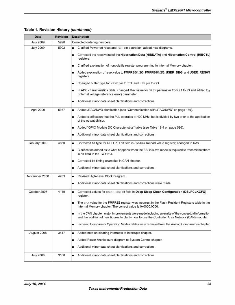
Table 1. Revision History (continued)
DescriptionRevisionDate
Corrected ordering numbers.5920July 2009
Clarified Power-on reset and RST pin operation; added new diagrams.
Corrected the reset value of the Hibernation Data (HIBDATA) and Hibernation Control (HIBCTL)registers.
Clarified explanation of nonvolatile register programming in Internal Memory chapter.
Added explanation of reset value to FMPRE0/1/2/3, FMPPE0/1/2/3,USER_DBG, andUSER_REG0/1registers.
Changed buffer type for WAKE pin to TTL and HIB pin to OD.
In ADC characteristics table, changed Max value for GAIN parameter from ±1 to ±3 and added EIR(Internal voltage reference error) parameter.
Additional minor data sheet clarifications and corrections.
5902July 2009
Added JTAG/SWD clarification (see “Communication with JTAG/SWD” on page 159).
Added clarification that the PLL operates at 400 MHz, but is divided by two prior to the applicationof the output divisor.
Added "GPIO Module DC Characteristics" table (see Table 19-4 on page 596).
Additional minor data sheet clarifications and corrections.
5367April 2009
Corrected bit type for RELOAD bit field in SysTick Reload Value register; changed to R/W.
Clarification added as to what happens when the SSI in slave mode is required to transmit but thereis no data in the TX FIFO.
Corrected bit timing examples in CAN chapter.
Additional minor data sheet clarifications and corrections.
4660January 2009
Revised High-Level Block Diagram.
Additional minor data sheet clarifications and corrections were made.
4283November 2008
Corrected values for DSOSCSRC bit field in Deep Sleep Clock Configuration (DSLPCLKCFG)register.
The FMA value for the FMPRE3 register was incorrect in the Flash Resident Registers table in theInternal Memory chapter. The correct value is 0x0000.0006.
In the CAN chapter, major improvements were made including a rewrite of the conceptual informationand the addition of new figures to clarify how to use the Controller Area Network (CAN) module.
Incorrect Comparator Operating Modes tables were removed from the Analog Comparators chapter.
4149October 2008
Added note on clearing interrupts to Interrupts chapter.
Added Power Architecture diagram to System Control chapter.
Additional minor data sheet clarifications and corrections.
3447August 2008
Additional minor data sheet clarifications and corrections.3108July 2008
25July 16, 2014Texas Instruments-Production Data
Stellaris® LM3S2601 Microcontroller
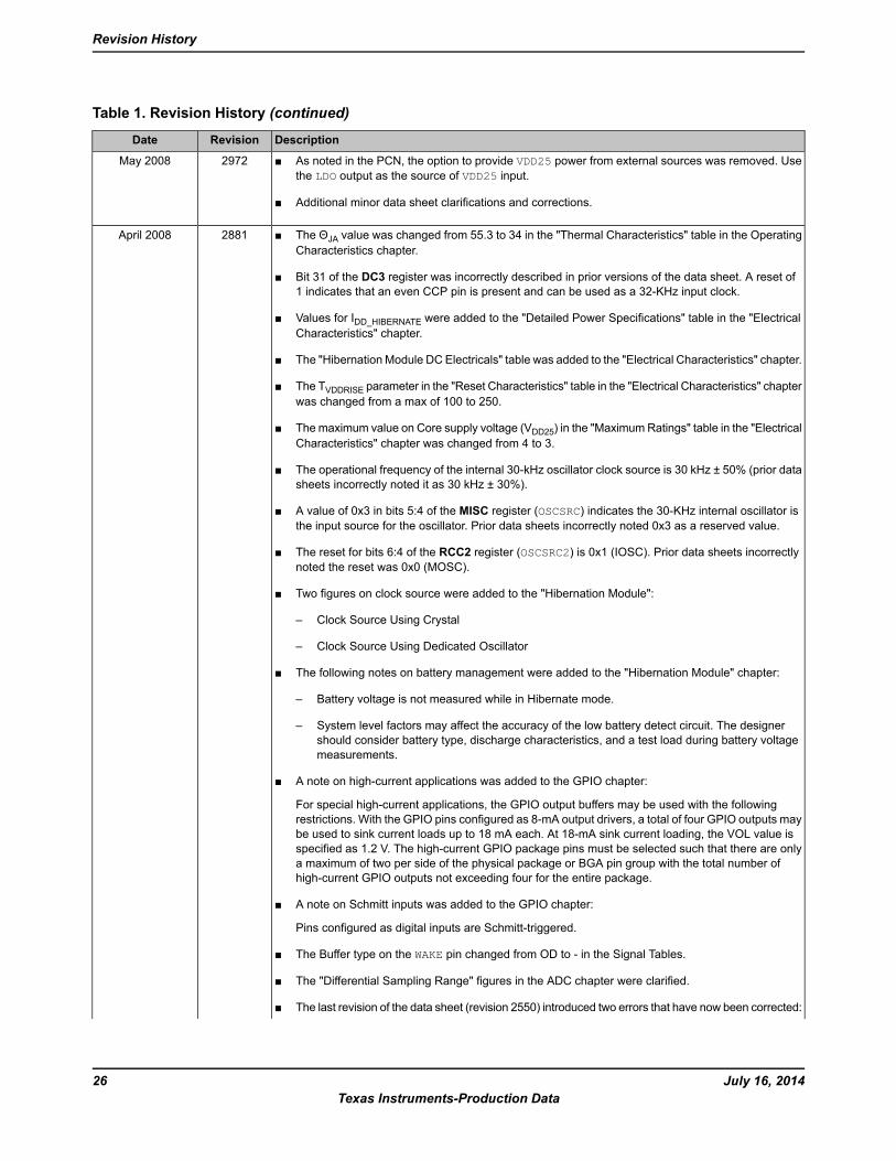
Table 1. Revision History (continued)
DescriptionRevisionDate
As noted in the PCN, the option to provide VDD25 power from external sources was removed. Usethe LDO output as the source of VDD25 input.
Additional minor data sheet clarifications and corrections.
2972May 2008
2881April 2008 The ΘJA value was changed from 55.3 to 34 in the "Thermal Characteristics" table in the OperatingCharacteristics chapter.
Bit 31 of the DC3 register was incorrectly described in prior versions of the data sheet. A reset of1 indicates that an even CCP pin is present and can be used as a 32-KHz input clock.
Values for IDD_HIBERNATE were added to the "Detailed Power Specifications" table in the "ElectricalCharacteristics" chapter.
The "Hibernation Module DC Electricals" table was added to the "Electrical Characteristics" chapter.
The TVDDRISE parameter in the "Reset Characteristics" table in the "Electrical Characteristics" chapterwas changed from a max of 100 to 250.
Themaximum value on Core supply voltage (VDD25) in the "MaximumRatings" table in the "ElectricalCharacteristics" chapter was changed from 4 to 3.
The operational frequency of the internal 30-kHz oscillator clock source is 30 kHz ± 50% (prior datasheets incorrectly noted it as 30 kHz ± 30%).
A value of 0x3 in bits 5:4 of the MISC register (OSCSRC) indicates the 30-KHz internal oscillator isthe input source for the oscillator. Prior data sheets incorrectly noted 0x3 as a reserved value.
The reset for bits 6:4 of the RCC2 register (OSCSRC2) is 0x1 (IOSC). Prior data sheets incorrectlynoted the reset was 0x0 (MOSC).
Two figures on clock source were added to the "Hibernation Module":
– Clock Source Using Crystal
– Clock Source Using Dedicated Oscillator
The following notes on battery management were added to the "Hibernation Module" chapter:
– Battery voltage is not measured while in Hibernate mode.
– System level factors may affect the accuracy of the low battery detect circuit. The designershould consider battery type, discharge characteristics, and a test load during battery voltagemeasurements.
A note on high-current applications was added to the GPIO chapter:
For special high-current applications, the GPIO output buffers may be used with the followingrestrictions. With the GPIO pins configured as 8-mA output drivers, a total of four GPIO outputs maybe used to sink current loads up to 18 mA each. At 18-mA sink current loading, the VOL value isspecified as 1.2 V. The high-current GPIO package pins must be selected such that there are onlya maximum of two per side of the physical package or BGA pin group with the total number ofhigh-current GPIO outputs not exceeding four for the entire package.
A note on Schmitt inputs was added to the GPIO chapter:
Pins configured as digital inputs are Schmitt-triggered.
The Buffer type on the WAKE pin changed from OD to - in the Signal Tables.
The "Differential Sampling Range" figures in the ADC chapter were clarified.
The last revision of the data sheet (revision 2550) introduced two errors that have now been corrected:
July 16, 201426Texas Instruments-Production Data
Revision History
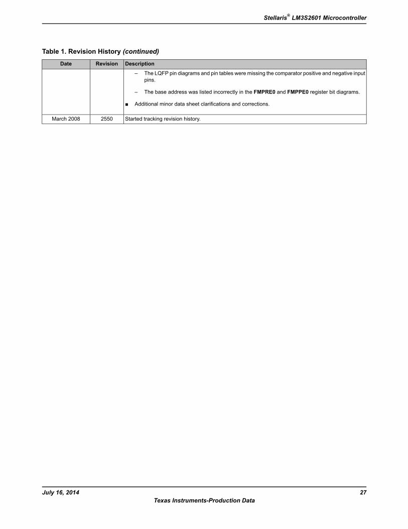
Table 1. Revision History (continued)
DescriptionRevisionDate
– The LQFP pin diagrams and pin tables were missing the comparator positive and negative inputpins.
– The base address was listed incorrectly in the FMPRE0 and FMPPE0 register bit diagrams.
Additional minor data sheet clarifications and corrections.
Started tracking revision history.2550March 2008
27July 16, 2014Texas Instruments-Production Data
Stellaris® LM3S2601 Microcontroller
About This DocumentThis data sheet provides reference information for the LM3S2601 microcontroller, describing thefunctional blocks of the system-on-chip (SoC) device designed around the ARM® Cortex™-M3core.
AudienceThis manual is intended for system software developers, hardware designers, and applicationdevelopers.
About This ManualThis document is organized into sections that correspond to each major feature.
Related DocumentsThe following related documents are available on the Stellaris® web site at www.ti.com/stellaris:
Stellaris® Errata
ARM® Cortex™-M3 Errata
Cortex™-M3/M4 Instruction Set Technical User's Manual
Stellaris® Graphics Library User's Guide
Stellaris® Peripheral Driver Library User's Guide
The following related documents are also referenced:
ARM® Debug Interface V5 Architecture Specification
ARM® Embedded Trace Macrocell Architecture Specification
IEEE Standard 1149.1-Test Access Port and Boundary-Scan Architecture
This documentation list was current as of publication date. Please check the web site for additionaldocumentation, including application notes and white papers.
July 16, 201428Texas Instruments-Production Data
About This Document
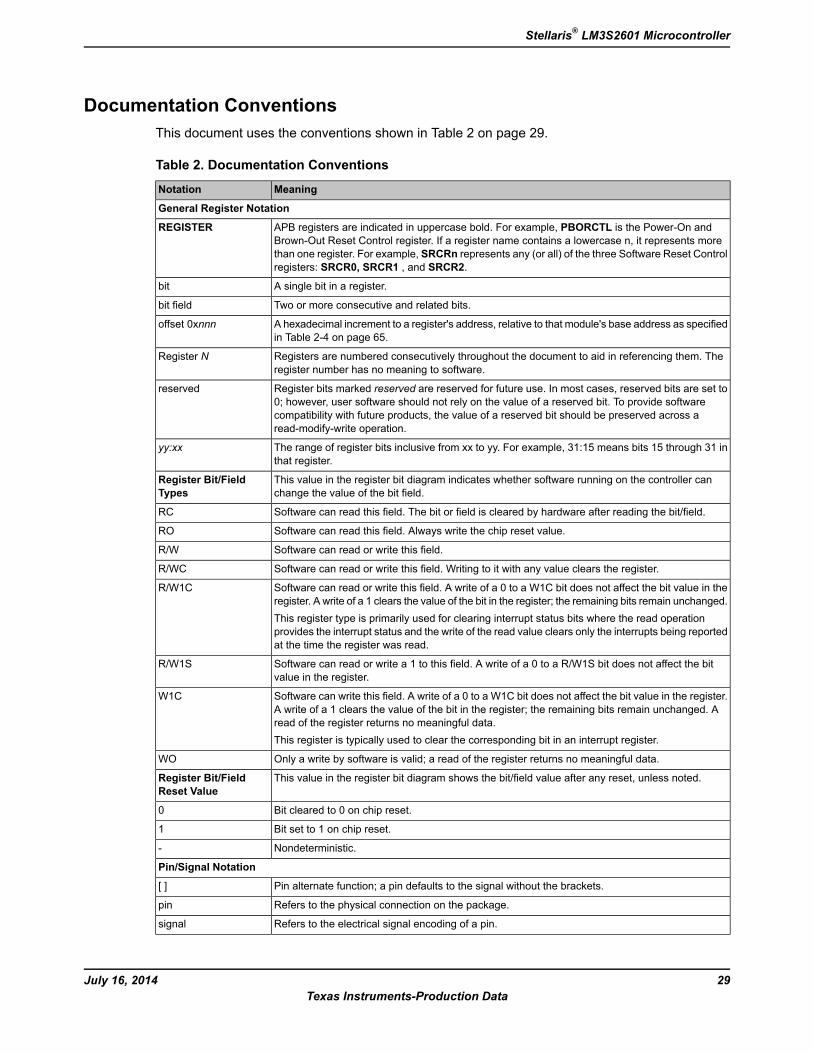
Documentation ConventionsThis document uses the conventions shown in Table 2 on page 29.
Table 2. Documentation Conventions
MeaningNotation
General Register Notation
APB registers are indicated in uppercase bold. For example, PBORCTL is the Power-On andBrown-Out Reset Control register. If a register name contains a lowercase n, it represents morethan one register. For example, SRCRn represents any (or all) of the three Software Reset Controlregisters: SRCR0, SRCR1 , and SRCR2.
REGISTER
A single bit in a register.bit
Two or more consecutive and related bits.bit field
A hexadecimal increment to a register's address, relative to that module's base address as specifiedin Table 2-4 on page 65.
offset 0xnnn
Registers are numbered consecutively throughout the document to aid in referencing them. Theregister number has no meaning to software.
Register N
Register bits marked reserved are reserved for future use. In most cases, reserved bits are set to0; however, user software should not rely on the value of a reserved bit. To provide softwarecompatibility with future products, the value of a reserved bit should be preserved across aread-modify-write operation.
reserved
The range of register bits inclusive from xx to yy. For example, 31:15 means bits 15 through 31 inthat register.
yy:xx
This value in the register bit diagram indicates whether software running on the controller canchange the value of the bit field.
Register Bit/FieldTypes
Software can read this field. The bit or field is cleared by hardware after reading the bit/field.RC
Software can read this field. Always write the chip reset value.RO
Software can read or write this field.R/W
Software can read or write this field. Writing to it with any value clears the register.R/WC
Software can read or write this field. A write of a 0 to a W1C bit does not affect the bit value in theregister. A write of a 1 clears the value of the bit in the register; the remaining bits remain unchanged.This register type is primarily used for clearing interrupt status bits where the read operationprovides the interrupt status and the write of the read value clears only the interrupts being reportedat the time the register was read.
R/W1C
Software can read or write a 1 to this field. A write of a 0 to a R/W1S bit does not affect the bitvalue in the register.
R/W1S
Software can write this field. A write of a 0 to a W1C bit does not affect the bit value in the register.A write of a 1 clears the value of the bit in the register; the remaining bits remain unchanged. Aread of the register returns no meaningful data.This register is typically used to clear the corresponding bit in an interrupt register.
W1C
Only a write by software is valid; a read of the register returns no meaningful data.WO
This value in the register bit diagram shows the bit/field value after any reset, unless noted.Register Bit/FieldReset Value
Bit cleared to 0 on chip reset.0
Bit set to 1 on chip reset.1
Nondeterministic.-
Pin/Signal Notation
Pin alternate function; a pin defaults to the signal without the brackets.[ ]
Refers to the physical connection on the package.pin
Refers to the electrical signal encoding of a pin.signal
29July 16, 2014Texas Instruments-Production Data
Stellaris® LM3S2601 Microcontroller
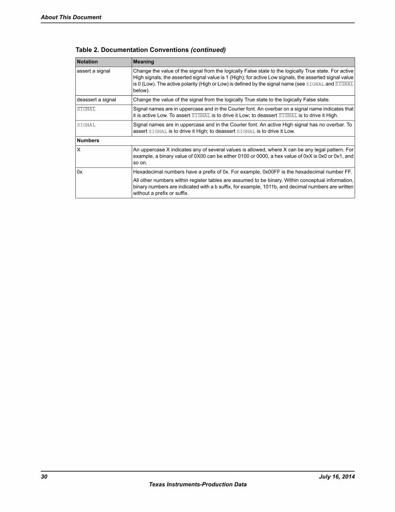
Table 2. Documentation Conventions (continued)
MeaningNotation
Change the value of the signal from the logically False state to the logically True state. For activeHigh signals, the asserted signal value is 1 (High); for active Low signals, the asserted signal valueis 0 (Low). The active polarity (High or Low) is defined by the signal name (see SIGNAL and SIGNALbelow).
assert a signal
Change the value of the signal from the logically True state to the logically False state.deassert a signal
Signal names are in uppercase and in the Courier font. An overbar on a signal name indicates thatit is active Low. To assert SIGNAL is to drive it Low; to deassert SIGNAL is to drive it High.
SIGNAL
Signal names are in uppercase and in the Courier font. An active High signal has no overbar. Toassert SIGNAL is to drive it High; to deassert SIGNAL is to drive it Low.
SIGNAL
Numbers
An uppercase X indicates any of several values is allowed, where X can be any legal pattern. Forexample, a binary value of 0X00 can be either 0100 or 0000, a hex value of 0xX is 0x0 or 0x1, andso on.
X
Hexadecimal numbers have a prefix of 0x. For example, 0x00FF is the hexadecimal number FF.All other numbers within register tables are assumed to be binary. Within conceptual information,binary numbers are indicated with a b suffix, for example, 1011b, and decimal numbers are writtenwithout a prefix or suffix.
0x
July 16, 201430Texas Instruments-Production Data
About This Document
1 Architectural OverviewThe Stellaris® family of microcontrollers—the first ARM® Cortex™-M3 based controllers—bringshigh-performance 32-bit computing to cost-sensitive embedded microcontroller applications. Thesepioneering parts deliver customers 32-bit performance at a cost equivalent to legacy 8- and 16-bitdevices, all in a package with a small footprint.
The Stellaris family offers efficient performance and extensive integration, favorably positioning thedevice into cost-conscious applications requiring significant control-processing and connectivitycapabilities. The Stellaris LM3S2000 series, designed for Controller Area Network (CAN) applications,extends the Stellaris family with Bosch CAN networking technology, the golden standard in short-haulindustrial networks. The Stellaris LM3S2000 series also marks the first integration of CAN capabilitieswith the revolutionary Cortex-M3 core.
The LM3S2601 microcontroller is targeted for industrial applications, including remote monitoring,electronic point-of-sale machines, test and measurement equipment, network appliances andswitches, factory automation, HVAC and building control, gaming equipment, motion control, medicalinstrumentation, and fire and security.
For applications requiring extreme conservation of power, the LM3S2601 microcontroller featuresa battery-backed Hibernation module to efficiently power down the LM3S2601 to a low-power stateduring extended periods of inactivity. With a power-up/power-down sequencer, a continuous timecounter (RTC), a pair of match registers, an APB interface to the system bus, and dedicatednon-volatile memory, the Hibernation module positions the LM3S2601 microcontroller perfectly forbattery applications.
In addition, the LM3S2601 microcontroller offers the advantages of ARM's widely availabledevelopment tools, System-on-Chip (SoC) infrastructure IP applications, and a large user community.Additionally, the microcontroller uses ARM's Thumb®-compatible Thumb-2 instruction set to reducememory requirements and, thereby, cost. Finally, the LM3S2601 microcontroller is code-compatibleto all members of the extensive Stellaris family; providing flexibility to fit our customers' preciseneeds.
Texas Instruments offers a complete solution to get to market quickly, with evaluation anddevelopment boards, white papers and application notes, an easy-to-use peripheral driver library,and a strong support, sales, and distributor network. See “Ordering and ContactInformation” on page 633 for ordering information for Stellaris family devices.
1.1 Product FeaturesThe LM3S2601 microcontroller includes the following product features:
32-Bit RISC Performance
– 32-bit ARM® Cortex™-M3 v7M architecture optimized for small-footprint embeddedapplications
– System timer (SysTick), providing a simple, 24-bit clear-on-write, decrementing, wrap-on-zerocounter with a flexible control mechanism
– Thumb®-compatible Thumb-2-only instruction set processor core for high code density
– 50-MHz operation
– Hardware-division and single-cycle-multiplication
31July 16, 2014Texas Instruments-Production Data
Stellaris® LM3S2601 Microcontroller
– Integrated Nested Vectored Interrupt Controller (NVIC) providing deterministic interrupthandling
– 30 interrupts with eight priority levels
– Memory protection unit (MPU), providing a privileged mode for protected operating systemfunctionality
– Unaligned data access, enabling data to be efficiently packed into memory
– Atomic bit manipulation (bit-banding), delivering maximummemory utilization and streamlinedperipheral control
ARM® Cortex™-M3 Processor Core
– Compact core.
– Thumb-2 instruction set, delivering the high-performance expected of an ARM core in thememory size usually associated with 8- and 16-bit devices; typically in the range of a fewkilobytes of memory for microcontroller class applications.
– Rapid application execution through Harvard architecture characterized by separate busesfor instruction and data.
– Exceptional interrupt handling, by implementing the register manipulations required for handlingan interrupt in hardware.
– Deterministic, fast interrupt processing: always 12 cycles, or just 6 cycles with tail-chaining
– Memory protection unit (MPU) to provide a privileged mode of operation for complexapplications.
– Migration from the ARM7™ processor family for better performance and power efficiency.
– Full-featured debug solution
• Serial Wire JTAG Debug Port (SWJ-DP)
• Flash Patch and Breakpoint (FPB) unit for implementing breakpoints
• Data Watchpoint and Trigger (DWT) unit for implementing watchpoints, trigger resources,and system profiling
• Instrumentation Trace Macrocell (ITM) for support of printf style debugging
• Trace Port Interface Unit (TPIU) for bridging to a Trace Port Analyzer
– Optimized for single-cycle flash usage
– Three sleep modes with clock gating for low power
– Single-cycle multiply instruction and hardware divide
– Atomic operations
– ARM Thumb2 mixed 16-/32-bit instruction set
July 16, 201432Texas Instruments-Production Data
Architectural Overview
– 1.25 DMIPS/MHz
JTAG
– IEEE 1149.1-1990 compatible Test Access Port (TAP) controller
– Four-bit Instruction Register (IR) chain for storing JTAG instructions
– IEEE standard instructions: BYPASS, IDCODE, SAMPLE/PRELOAD, EXTEST and INTEST
– ARM additional instructions: APACC, DPACC and ABORT
– Integrated ARM Serial Wire Debug (SWD)
Hibernation
– System power control using discrete external regulator
– Dedicated pin for waking from an external signal
– Low-battery detection, signaling, and interrupt generation
– 32-bit real-time clock (RTC)
– Two 32-bit RTC match registers for timed wake-up and interrupt generation
– Clock source from a 32.768-kHz external oscillator or a 4.194304-MHz crystal
– RTC predivider trim for making fine adjustments to the clock rate
– 64 32-bit words of non-volatile memory
– Programmable interrupts for RTC match, external wake, and low battery events
Internal Memory
– 128 KB single-cycle flash
• User-managed flash block protection on a 2-KB block basis
• User-managed flash data programming
• User-defined and managed flash-protection block
– 32 KB single-cycle SRAM
GPIOs
– 21-60 GPIOs, depending on configuration
– 5-V-tolerant in input configuration
– Fast toggle capable of a change every two clock cycles
– Programmable control for GPIO interrupts
• Interrupt generation masking
33July 16, 2014Texas Instruments-Production Data
Stellaris® LM3S2601 Microcontroller
• Edge-triggered on rising, falling, or both
• Level-sensitive on High or Low values
– Bit masking in both read and write operations through address lines
– Pins configured as digital inputs are Schmitt-triggered.
– Programmable control for GPIO pad configuration
• Weak pull-up or pull-down resistors
• 2-mA, 4-mA, and 8-mA pad drive for digital communication; up to four pads can beconfigured with an 18-mA pad drive for high-current applications
• Slew rate control for the 8-mA drive
• Open drain enables
• Digital input enables
General-Purpose Timers
– Four General-Purpose Timer Modules (GPTM), each of which provides two 16-bittimers/counters. Each GPTM can be configured to operate independently:
• As a single 32-bit timer
• As one 32-bit Real-Time Clock (RTC) to event capture
• For Pulse Width Modulation (PWM)
– 32-bit Timer modes
• Programmable one-shot timer
• Programmable periodic timer
• Real-Time Clock when using an external 32.768-KHz clock as the input
• User-enabled stalling when the controller asserts CPU Halt flag during debug
– 16-bit Timer modes
• General-purpose timer function with an 8-bit prescaler (for one-shot and periodic modesonly)
• Programmable one-shot timer
• Programmable periodic timer
• User-enabled stalling when the controller asserts CPU Halt flag during debug
– 16-bit Input Capture modes
• Input edge count capture
July 16, 201434Texas Instruments-Production Data
Architectural Overview
• Input edge time capture
– 16-bit PWM mode
• Simple PWM mode with software-programmable output inversion of the PWM signal
ARM FiRM-compliant Watchdog Timer
– 32-bit down counter with a programmable load register
– Separate watchdog clock with an enable
– Programmable interrupt generation logic with interrupt masking
– Lock register protection from runaway software
– Reset generation logic with an enable/disable
– User-enabled stalling when the controller asserts the CPU Halt flag during debug
UART
– Three fully programmable 16C550-type UARTs with IrDA support
– Separate 16x8 transmit (TX) and receive (RX) FIFOs to reduce CPU interrupt service loading
– Programmable baud-rate generator allowing speeds up to 3.125 Mbps
– Programmable FIFO length, including 1-byte deep operation providing conventionaldouble-buffered interface
– FIFO trigger levels of 1/8, 1/4, 1/2, 3/4, and 7/8
– Standard asynchronous communication bits for start, stop, and parity
– Line-break generation and detection
– Fully programmable serial interface characteristics
• 5, 6, 7, or 8 data bits
• Even, odd, stick, or no-parity bit generation/detection
• 1 or 2 stop bit generation
– IrDA serial-IR (SIR) encoder/decoder providing
• Programmable use of IrDA Serial Infrared (SIR) or UART input/output
• Support of IrDA SIR encoder/decoder functions for data rates up to 115.2 Kbps half-duplex
• Support of normal 3/16 and low-power (1.41-2.23 μs) bit durations
• Programmable internal clock generator enabling division of reference clock by 1 to 256for low-power mode bit duration
Synchronous Serial Interface (SSI)
35July 16, 2014Texas Instruments-Production Data
Stellaris® LM3S2601 Microcontroller
– Two SSI modules, each with the following features:
– Master or slave operation
– Programmable clock bit rate and prescale
– Separate transmit and receive FIFOs, 16 bits wide, 8 locations deep
– Programmable interface operation for Freescale SPI, MICROWIRE, or Texas Instrumentssynchronous serial interfaces
– Programmable data frame size from 4 to 16 bits
– Internal loopback test mode for diagnostic/debug testing
I2C
– Two I2C modules, each with the following features:
– Devices on the I2C bus can be designated as either a master or a slave
• Supports both sending and receiving data as either a master or a slave
• Supports simultaneous master and slave operation
– Four I2C modes
• Master transmit
• Master receive
• Slave transmit
• Slave receive
– Two transmission speeds: Standard (100 Kbps) and Fast (400 Kbps)
– Master and slave interrupt generation
• Master generates interrupts when a transmit or receive operation completes (or abortsdue to an error)
• Slave generates interrupts when data has been sent or requested by a master
– Master with arbitration and clock synchronization, multimaster support, and 7-bit addressingmode
Controller Area Network (CAN)
– CAN protocol version 2.0 part A/B
– Bit rates up to 1 Mbps
– 32 message objects with individual identifier masks
– Maskable interrupt
July 16, 201436Texas Instruments-Production Data
Architectural Overview
– Disable Automatic Retransmission mode for Time-Triggered CAN (TTCAN) applications
– Programmable Loopback mode for self-test operation
– Programmable FIFO mode enables storage of multiple message objects
– Gluelessly attaches to an external CAN interface through the CANnTX and CANnRX signals
Analog Comparators
– Two independent integrated analog comparators
– Configurable for output to drive an output pin or generate an interrupt
– Compare external pin input to external pin input or to internal programmable voltage reference
– Compare a test voltage against any one of these voltages
• An individual external reference voltage
• A shared single external reference voltage
• A shared internal reference voltage
Power
– On-chip Low Drop-Out (LDO) voltage regulator, with programmable output user-adjustablefrom 2.25 V to 2.75 V
– Hibernation module handles the power-up/down 3.3 V sequencing and control for the coredigital logic and analog circuits
– Low-power options on controller: Sleep and Deep-sleep modes
– Low-power options for peripherals: software controls shutdown of individual peripherals
– 3.3-V supply brown-out detection and reporting via interrupt or reset
Flexible Reset Sources
– Power-on reset (POR)
– Reset pin assertion
– Brown-out (BOR) detector alerts to system power drops
– Software reset
– Watchdog timer reset
– Internal low drop-out (LDO) regulator output goes unregulated
Industrial temperature 100-pin RoHS-compliant LQFP package
Industrial-range 108-ball RoHS-compliant BGA package
37July 16, 2014Texas Instruments-Production Data
Stellaris® LM3S2601 Microcontroller
1.2 Target Applications Remote monitoring
Electronic point-of-sale (POS) machines
Test and measurement equipment
Network appliances and switches
Factory automation
HVAC and building control
Gaming equipment
Motion control
Medical instrumentation
Fire and security
Power and energy
Transportation
1.3 High-Level Block DiagramFigure 1-1 on page 39 depicts the features on the Stellaris LM3S2601 microcontroller.
July 16, 201438Texas Instruments-Production Data
Architectural Overview
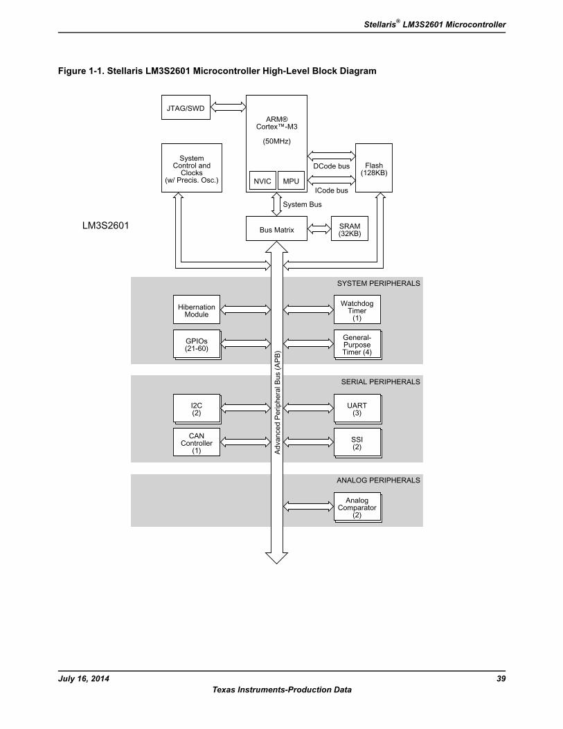
Figure 1-1. Stellaris LM3S2601 Microcontroller High-Level Block Diagram
ARM®Cortex™-M3
(50MHz)
NVIC MPU
Flash(128KB)
DCode bus
ICode bus
JTAG/SWD
SystemControl andClocks
(w/ Precis. Osc.)
Bus Matrix
System Bus
SRAM(32KB)
SYSTEM PERIPHERALS
WatchdogTimer(1)
HibernationModule
General-PurposeTimer (4)
GPIOs(21-60)
SERIAL PERIPHERALS
UART(3)
I2C(2)
SSI(2)
CANController
(1)
ANALOG PERIPHERALS
AnalogComparator
(2)
Advanced
PeripheralB
us(APB
)
LM3S2601
39July 16, 2014Texas Instruments-Production Data
Stellaris® LM3S2601 Microcontroller
1.4 Functional OverviewThe following sections provide an overview of the features of the LM3S2601 microcontroller. Thepage number in parenthesis indicates where that feature is discussed in detail. Ordering and supportinformation can be found in “Ordering and Contact Information” on page 633.
1.4.1 ARM Cortex™-M3
1.4.1.1 Processor Core (see page 46)All members of the Stellaris product family, including the LM3S2601 microcontroller, are designedaround an ARM Cortex™-M3 processor core. The ARM Cortex-M3 processor provides the core fora high-performance, low-cost platform that meets the needs of minimal memory implementation,reduced pin count, and low-power consumption, while delivering outstanding computationalperformance and exceptional system response to interrupts.
1.4.1.2 Memory Map (see page 65)A memory map lists the location of instructions and data in memory. The memory map for theLM3S2601 controller can be found in Table 2-4 on page 65. Register addresses are given as ahexadecimal increment, relative to the module's base address as shown in the memory map.
1.4.1.3 System Timer (SysTick) (see page 88)Cortex-M3 includes an integrated system timer, SysTick. SysTick provides a simple, 24-bitclear-on-write, decrementing, wrap-on-zero counter with a flexible control mechanism. The countercan be used in several different ways, for example:
An RTOS tick timer which fires at a programmable rate (for example, 100 Hz) and invokes aSysTick routine.
A high-speed alarm timer using the system clock.
A variable rate alarm or signal timer—the duration is range-dependent on the reference clockused and the dynamic range of the counter.
A simple counter. Software can use this to measure time to completion and time used.
An internal clock source control based on missing/meeting durations. The COUNTFLAG bit-fieldin the control and status register can be used to determine if an action completed within a setduration, as part of a dynamic clock management control loop.
1.4.1.4 Nested Vectored Interrupt Controller (NVIC) (see page 89)The LM3S2601 controller includes the ARM Nested Vectored Interrupt Controller (NVIC) on theARM®Cortex™-M3 core. The NVIC and Cortex-M3 prioritize and handle all exceptions. All exceptionsare handled in Handler Mode. The processor state is automatically stored to the stack on anexception, and automatically restored from the stack at the end of the Interrupt Service Routine(ISR). The vector is fetched in parallel to the state saving, which enables efficient interrupt entry.The processor supports tail-chaining, which enables back-to-back interrupts to be performed withoutthe overhead of state saving and restoration. Software can set eight priority levels on 7 exceptions(system handlers) and 30 interrupts.
July 16, 201440Texas Instruments-Production Data
Architectural Overview
1.4.1.5 System Control Block (SCB) (see page 91)The SCB provides system implementation information and system control, including configuration,control, and reporting of system exceptions.
1.4.1.6 Memory Protection Unit (MPU) (see page 91)The MPU supports the standard ARMv7 Protected Memory System Architecture (PMSA) model.The MPU provides full support for protection regions, overlapping protection regions, accesspermissions, and exporting memory attributes to the system.
1.4.2 Motor Control PeripheralsTo enhancemotor control, the LM3S2601 controller features PulseWidth Modulation (PWM) outputs.
1.4.2.1 PWMPulse width modulation (PWM) is a powerful technique for digitally encoding analog signal levels.High-resolution counters are used to generate a square wave, and the duty cycle of the squarewave is modulated to encode an analog signal. Typical applications include switching power suppliesand motor control.
On the LM3S2601, PWM motion control functionality can be achieved through:
The motion control features of the general-purpose timers using the CCP pins
CCP Pins (see page 334)
TheGeneral-Purpose TimerModule's CCP (Capture Compare PWM) pins are software programmableto support a simple PWMmode with a software-programmable output inversion of the PWM signal.
1.4.3 Analog PeripheralsFor support of analog signals, the LM3S2601 microcontroller offers two analog comparators.
1.4.3.1 Analog Comparators (see page 553)An analog comparator is a peripheral that compares two analog voltages, and provides a logicaloutput that signals the comparison result.
The LM3S2601 microcontroller provides two independent integrated analog comparators that canbe configured to drive an output or generate an interrupt .
A comparator can compare a test voltage against any one of these voltages:
An individual external reference voltage
A shared single external reference voltage
A shared internal reference voltage
The comparator can provide its output to a device pin, acting as a replacement for an analogcomparator on the board, or it can be used to signal the application via interrupts to cause it to startcapturing a sample sequence.
1.4.4 Serial Communications PeripheralsThe LM3S2601 controller supports both asynchronous and synchronous serial communicationswith:
41July 16, 2014Texas Instruments-Production Data
Stellaris® LM3S2601 Microcontroller
Three fully programmable 16C550-type UARTs
Two SSI modules
Two I2C modules
One CAN unit
1.4.4.1 UART (see page 388)A Universal Asynchronous Receiver/Transmitter (UART) is an integrated circuit used for RS-232Cserial communications, containing a transmitter (parallel-to-serial converter) and a receiver(serial-to-parallel converter), each clocked separately.
The LM3S2601 controller includes three fully programmable 16C550-type UARTs that support datatransfer speeds up to 3.125 Mbps. (Although similar in functionality to a 16C550 UART, it is notregister-compatible.) In addition, each UART is capable of supporting IrDA.
Separate 16x8 transmit (TX) and receive (RX) FIFOs reduce CPU interrupt service loading. TheUART can generate individually masked interrupts from the RX, TX, modem status, and errorconditions. The module provides a single combined interrupt when any of the interrupts are assertedand are unmasked.
1.4.4.2 SSI (see page 431)Synchronous Serial Interface (SSI) is a four-wire bi-directional full and low-speed communicationsinterface.
The LM3S2601 controller includes two SSI modules that provide the functionality for synchronousserial communications with peripheral devices, and can be configured to use the Freescale SPI,MICROWIRE, or TI synchronous serial interface frame formats. The size of the data frame is alsoconfigurable, and can be set between 4 and 16 bits, inclusive.
Each SSI module performs serial-to-parallel conversion on data received from a peripheral device,and parallel-to-serial conversion on data transmitted to a peripheral device. The TX and RX pathsare buffered with internal FIFOs, allowing up to eight 16-bit values to be stored independently.
Each SSI module can be configured as either a master or slave device. As a slave device, the SSImodule can also be configured to disable its output, which allows a master device to be coupledwith multiple slave devices.
Each SSI module also includes a programmable bit rate clock divider and prescaler to generate theoutput serial clock derived from the SSI module's input clock. Bit rates are generated based on theinput clock and the maximum bit rate is determined by the connected peripheral.
1.4.4.3 I2C (see page 469)The Inter-Integrated Circuit (I2C) bus provides bi-directional data transfer through a two-wire design(a serial data line SDA and a serial clock line SCL).
The I2C bus interfaces to external I2C devices such as serial memory (RAMs and ROMs), networkingdevices, LCDs, tone generators, and so on. The I2C bus may also be used for system testing anddiagnostic purposes in product development and manufacture.
The LM3S2601 controller includes two I2C modules that provide the ability to communicate to otherIC devices over an I2C bus. The I2C bus supports devices that can both transmit and receive (writeand read) data.
July 16, 201442Texas Instruments-Production Data
Architectural Overview
Devices on the I2C bus can be designated as either a master or a slave. Each I2C module supportsboth sending and receiving data as either a master or a slave, and also supports the simultaneousoperation as both a master and a slave. The four I2C modes are: Master Transmit, Master Receive,Slave Transmit, and Slave Receive.
A Stellaris I2C module can operate at two speeds: Standard (100 Kbps) and Fast (400 Kbps).
Both the I2C master and slave can generate interrupts. The I2C master generates interrupts whena transmit or receive operation completes (or aborts due to an error). The I2C slave generatesinterrupts when data has been sent or requested by a master.
1.4.4.4 Controller Area Network (see page 506)Controller Area Network (CAN) is a multicast shared serial-bus standard for connecting electroniccontrol units (ECUs). CAN was specifically designed to be robust in electromagnetically noisyenvironments and can utilize a differential balanced line like RS-485 or a more robust twisted-pairwire. Originally created for automotive purposes, now it is used in many embedded controlapplications (for example, industrial or medical). Bit rates up to 1Mb/s are possible at network lengthsbelow 40 meters. Decreased bit rates allow longer network distances (for example, 125 Kb/s at500m).
A transmitter sends a message to all CAN nodes (broadcasting). Each node decides on the basisof the identifier received whether it should process the message. The identifier also determines thepriority that the message enjoys in competition for bus access. Each CAN message can transmitfrom 0 to 8 bytes of user information. The LM3S2601 includes one CAN unit.
1.4.5 System Peripherals
1.4.5.1 Programmable GPIOs (see page 279)General-purpose input/output (GPIO) pins offer flexibility for a variety of connections.
The Stellaris GPIO module is comprised of eight physical GPIO blocks, each corresponding to anindividual GPIO port. The GPIO module is FiRM-compliant (compliant to the ARM Foundation IPfor Real-Time Microcontrollers specification) and supports 21-60 programmable input/output pins.The number of GPIOs available depends on the peripherals being used (see “SignalTables” on page 567 for the signals available to each GPIO pin).
The GPIO module features programmable interrupt generation as either edge-triggered orlevel-sensitive on all pins, programmable control for GPIO pad configuration, and bit masking inboth read and write operations through address lines. Pins configured as digital inputs areSchmitt-triggered.
1.4.5.2 Four Programmable Timers (see page 327)Programmable timers can be used to count or time external events that drive the Timer input pins.
The Stellaris General-Purpose Timer Module (GPTM) contains four GPTM blocks. Each GPTMblock provides two 16-bit timers/counters that can be configured to operate independently as timersor event counters, or configured to operate as one 32-bit timer or one 32-bit Real-Time Clock (RTC).
When configured in 32-bit mode, a timer can run as a Real-Time Clock (RTC), one-shot timer orperiodic timer. When in 16-bit mode, a timer can run as a one-shot timer or periodic timer, and canextend its precision by using an 8-bit prescaler. A 16-bit timer can also be configured for eventcapture or Pulse Width Modulation (PWM) generation.
43July 16, 2014Texas Instruments-Production Data
Stellaris® LM3S2601 Microcontroller
1.4.5.3 Watchdog Timer (see page 364)A watchdog timer can generate an interrupt or a reset when a time-out value is reached. Thewatchdog timer is used to regain control when a system has failed due to a software error or to thefailure of an external device to respond in the expected way.
The Stellaris Watchdog Timer module consists of a 32-bit down counter, a programmable loadregister, interrupt generation logic, and a locking register.
The Watchdog Timer can be configured to generate an interrupt to the controller on its first time-out,and to generate a reset signal on its second time-out. Once theWatchdog Timer has been configured,the lock register can be written to prevent the timer configuration from being inadvertently altered.
1.4.6 Memory PeripheralsThe LM3S2601 controller offers both single-cycle SRAM and single-cycle Flash memory.
1.4.6.1 SRAM (see page 252)The LM3S2601 static random access memory (SRAM) controller supports 32 KB SRAM. The internalSRAM of the Stellaris devices starts at base address 0x2000.0000 of the device memory map. Toreduce the number of time-consuming read-modify-write (RMW) operations, ARM has introducedbit-banding technology in the new Cortex-M3 processor. With a bit-band-enabled processor, certainregions in the memory map (SRAM and peripheral space) can use address aliases to accessindividual bits in a single, atomic operation.
1.4.6.2 Flash (see page 253)The LM3S2601 Flash controller supports 128 KB of flash memory. The flash is organized as a setof 1-KB blocks that can be individually erased. Erasing a block causes the entire contents of theblock to be reset to all 1s. These blocks are paired into a set of 2-KB blocks that can be individuallyprotected. The blocks can be marked as read-only or execute-only, providing different levels of codeprotection. Read-only blocks cannot be erased or programmed, protecting the contents of thoseblocks from being modified. Execute-only blocks cannot be erased or programmed, and can onlybe read by the controller instruction fetch mechanism, protecting the contents of those blocks frombeing read by either the controller or by a debugger.
1.4.7 Additional Features
1.4.7.1 JTAG TAP Controller (see page 152)The Joint Test Action Group (JTAG) port is an IEEE standard that defines a Test Access Port andBoundary Scan Architecture for digital integrated circuits and provides a standardized serial interfacefor controlling the associated test logic. The TAP, Instruction Register (IR), and Data Registers (DR)can be used to test the interconnections of assembled printed circuit boards and obtain manufacturinginformation on the components. The JTAG Port also provides a means of accessing and controllingdesign-for-test features such as I/O pin observation and control, scan testing, and debugging.
The JTAG port is composed of the standard five pins: TRST, TCK, TMS, TDI, and TDO. Data istransmitted serially into the controller on TDI and out of the controller on TDO. The interpretation ofthis data is dependent on the current state of the TAP controller. For detailed information on theoperation of the JTAG port and TAP controller, please refer to the IEEE Standard 1149.1-TestAccess Port and Boundary-Scan Architecture.
The Stellaris JTAG controller works with the ARM JTAG controller built into the Cortex-M3 core.This is implemented by multiplexing the TDO outputs from both JTAG controllers. ARM JTAGinstructions select the ARM TDO output while Stellaris JTAG instructions select the Stellaris TDO
July 16, 201444Texas Instruments-Production Data
Architectural Overview
outputs. The multiplexer is controlled by the Stellaris JTAG controller, which has comprehensiveprogramming for the ARM, Stellaris, and unimplemented JTAG instructions.
1.4.7.2 System Control and Clocks (see page 165)System control determines the overall operation of the device. It provides information about thedevice, controls the clocking of the device and individual peripherals, and handles reset detectionand reporting.
1.4.7.3 Hibernation Module (see page 231)The Hibernation module provides logic to switch power off to the main processor and peripherals,and to wake on external or time-based events. The Hibernation module includes power-sequencinglogic, a real-time clock with a pair of match registers, low-battery detection circuitry, and interruptsignalling to the processor. It also includes 64 32-bit words of non-volatile memory that can be usedfor saving state during hibernation.
1.4.8 Hardware DetailsDetails on the pins and package can be found in the following sections:
“Pin Diagram” on page 565
“Signal Tables” on page 567
“Operating Characteristics” on page 594
“Electrical Characteristics” on page 595
“Package Information” on page 635
45July 16, 2014Texas Instruments-Production Data
Stellaris® LM3S2601 Microcontroller
2 The Cortex-M3 ProcessorThe ARM® Cortex™-M3 processor provides a high-performance, low-cost platform that meets thesystem requirements of minimal memory implementation, reduced pin count, and low powerconsumption, while delivering outstanding computational performance and exceptional systemresponse to interrupts. Features include:
Compact core.
Thumb-2 instruction set, delivering the high-performance expected of an ARM core in the memorysize usually associated with 8- and 16-bit devices; typically in the range of a few kilobytes ofmemory for microcontroller class applications.
Rapid application execution through Harvard architecture characterized by separate buses forinstruction and data.
Exceptional interrupt handling, by implementing the register manipulations required for handlingan interrupt in hardware.
Deterministic, fast interrupt processing: always 12 cycles, or just 6 cycles with tail-chaining
Memory protection unit (MPU) to provide a privileged mode of operation for complex applications.
Migration from the ARM7™ processor family for better performance and power efficiency.
Full-featured debug solution
– Serial Wire JTAG Debug Port (SWJ-DP)
– Flash Patch and Breakpoint (FPB) unit for implementing breakpoints
– Data Watchpoint and Trigger (DWT) unit for implementing watchpoints, trigger resources,and system profiling
– Instrumentation Trace Macrocell (ITM) for support of printf style debugging
– Trace Port Interface Unit (TPIU) for bridging to a Trace Port Analyzer
Optimized for single-cycle flash usage
Three sleep modes with clock gating for low power
Single-cycle multiply instruction and hardware divide
Atomic operations
ARM Thumb2 mixed 16-/32-bit instruction set
1.25 DMIPS/MHz
The Stellaris® family of microcontrollers builds on this core to bring high-performance 32-bit computingto cost-sensitive embedded microcontroller applications, such as factory automation and control,industrial control power devices, building and home automation, and stepper motor control.
July 16, 201446Texas Instruments-Production Data
The Cortex-M3 Processor
This chapter provides information on the Stellaris implementation of the Cortex-M3 processor,including the programming model, the memory model, the exception model, fault handling, andpower management.
For technical details on the instruction set, see theCortex™-M3/M4 Instruction Set Technical User'sManual.
2.1 Block DiagramThe Cortex-M3 processor is built on a high-performance processor core, with a 3-stage pipelineHarvard architecture, making it ideal for demanding embedded applications. The processor deliversexceptional power efficiency through an efficient instruction set and extensively optimized design,providing high-end processing hardware including a range of single-cycle and SIMD multiplicationand multiply-with-accumulate capabilities, saturating arithmetic and dedicated hardware division.
To facilitate the design of cost-sensitive devices, the Cortex-M3 processor implements tightly coupledsystem components that reduce processor area while significantly improving interrupt handling andsystem debug capabilities. The Cortex-M3 processor implements a version of the Thumb® instructionset based on Thumb-2 technology, ensuring high code density and reduced program memoryrequirements. The Cortex-M3 instruction set provides the exceptional performance expected of amodern 32-bit architecture, with the high code density of 8-bit and 16-bit microcontrollers.
The Cortex-M3 processor closely integrates a nested interrupt controller (NVIC), to deliverindustry-leading interrupt performance. The Stellaris NVIC includes a non-maskable interrupt (NMI)and provides eight interrupt priority levels. The tight integration of the processor core and NVICprovides fast execution of interrupt service routines (ISRs), dramatically reducing interrupt latency.The hardware stacking of registers and the ability to suspend load-multiple and store-multipleoperations further reduce interrupt latency. Interrupt handlers do not require any assembler stubswhich removes code overhead from the ISRs. Tail-chaining optimization also significantly reducesthe overhead when switching from one ISR to another. To optimize low-power designs, the NVICintegrates with the sleep modes, including Deep-sleep mode, which enables the entire device to berapidly powered down.
47July 16, 2014Texas Instruments-Production Data
Stellaris® LM3S2601 Microcontroller
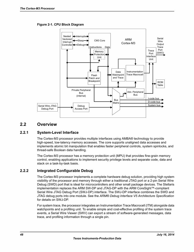
Figure 2-1. CPU Block Diagram
Private PeripheralBus
(internal)
DataWatchpointand Trace
Interrupts
Debug
Sleep
InstrumentationTrace Macrocell
TracePort
InterfaceUnit
CM3 Core
Instructions Data
FlashPatch andBreakpoint
MemoryProtection
Unit
DebugAccess Port
NestedVectoredInterruptController
Serial Wire JTAGDebug Port
BusMatrix
Adv. PeripheralBus
I-code busD-code busSystem bus
ROMTable
SerialWireOutputTracePort
(SWO)
ARMCortex-M3
2.2 Overview
2.2.1 System-Level InterfaceThe Cortex-M3 processor provides multiple interfaces using AMBA® technology to providehigh-speed, low-latency memory accesses. The core supports unaligned data accesses andimplements atomic bit manipulation that enables faster peripheral controls, system spinlocks, andthread-safe Boolean data handling.
The Cortex-M3 processor has a memory protection unit (MPU) that provides fine-grain memorycontrol, enabling applications to implement security privilege levels and separate code, data andstack on a task-by-task basis.
2.2.2 Integrated Configurable DebugThe Cortex-M3 processor implements a complete hardware debug solution, providing high systemvisibility of the processor and memory through either a traditional JTAG port or a 2-pin Serial WireDebug (SWD) port that is ideal for microcontrollers and other small package devices. The Stellarisimplementation replaces the ARM SW-DP and JTAG-DP with the ARM CoreSight™-compliantSerial Wire JTAG Debug Port (SWJ-DP) interface. The SWJ-DP interface combines the SWD andJTAG debug ports into one module. See the ARM® Debug Interface V5 Architecture Specificationfor details on SWJ-DP.
For system trace, the processor integrates an Instrumentation Trace Macrocell (ITM) alongside datawatchpoints and a profiling unit. To enable simple and cost-effective profiling of the system traceevents, a Serial Wire Viewer (SWV) can export a stream of software-generated messages, datatrace, and profiling information through a single pin.
July 16, 201448Texas Instruments-Production Data
The Cortex-M3 Processor
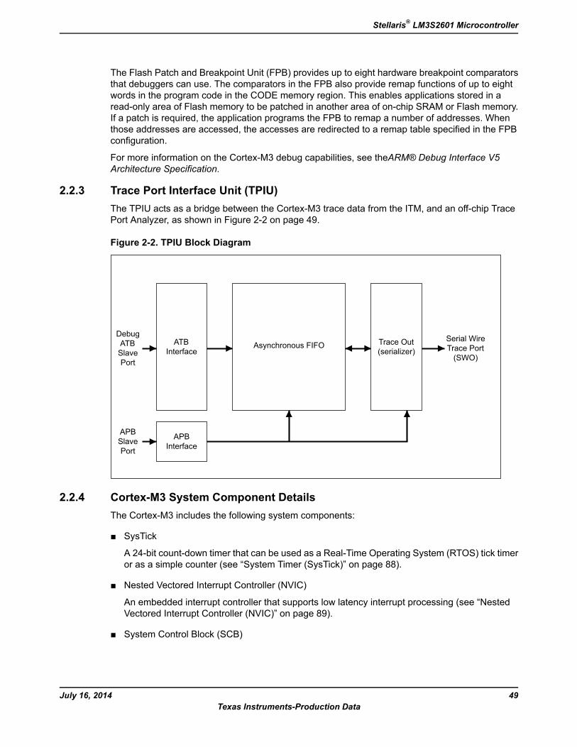
The Flash Patch and Breakpoint Unit (FPB) provides up to eight hardware breakpoint comparatorsthat debuggers can use. The comparators in the FPB also provide remap functions of up to eightwords in the program code in the CODE memory region. This enables applications stored in aread-only area of Flash memory to be patched in another area of on-chip SRAM or Flash memory.If a patch is required, the application programs the FPB to remap a number of addresses. Whenthose addresses are accessed, the accesses are redirected to a remap table specified in the FPBconfiguration.
For more information on the Cortex-M3 debug capabilities, see theARM® Debug Interface V5Architecture Specification.
2.2.3 Trace Port Interface Unit (TPIU)The TPIU acts as a bridge between the Cortex-M3 trace data from the ITM, and an off-chip TracePort Analyzer, as shown in Figure 2-2 on page 49.
Figure 2-2. TPIU Block Diagram
ATBInterface
Asynchronous FIFO
APBInterface
Trace Out(serializer)
DebugATBSlavePort
APBSlavePort
Serial WireTrace Port(SWO)
2.2.4 Cortex-M3 System Component DetailsThe Cortex-M3 includes the following system components:
SysTick
A 24-bit count-down timer that can be used as a Real-Time Operating System (RTOS) tick timeror as a simple counter (see “System Timer (SysTick)” on page 88).
Nested Vectored Interrupt Controller (NVIC)
An embedded interrupt controller that supports low latency interrupt processing (see “NestedVectored Interrupt Controller (NVIC)” on page 89).
System Control Block (SCB)
49July 16, 2014Texas Instruments-Production Data
Stellaris® LM3S2601 Microcontroller
The programming model interface to the processor. The SCB provides system implementationinformation and system control, including configuration, control, and reporting of system exceptions(see “System Control Block (SCB)” on page 91).
Memory Protection Unit (MPU)
Improves system reliability by defining the memory attributes for different memory regions. TheMPU provides up to eight different regions and an optional predefined background region (see“Memory Protection Unit (MPU)” on page 91).
2.3 Programming ModelThis section describes the Cortex-M3 programming model. In addition to the individual core registerdescriptions, information about the processor modes and privilege levels for software execution andstacks is included.
2.3.1 Processor Mode and Privilege Levels for Software ExecutionThe Cortex-M3 has two modes of operation:
Thread mode
Used to execute application software. The processor enters Thread mode when it comes out ofreset.
Handler mode
Used to handle exceptions. When the processor has finished exception processing, it returns toThread mode.
In addition, the Cortex-M3 has two privilege levels:
Unprivileged
In this mode, software has the following restrictions:
– Limited access to the MSR and MRS instructions and no use of the CPS instruction
– No access to the system timer, NVIC, or system control block
– Possibly restricted access to memory or peripherals
Privileged
In this mode, software can use all the instructions and has access to all resources.
In Thread mode, the CONTROL register (see page 64) controls whether software execution isprivileged or unprivileged. In Handler mode, software execution is always privileged.
Only privileged software can write to theCONTROL register to change the privilege level for softwareexecution in Thread mode. Unprivileged software can use the SVC instruction to make a supervisorcall to transfer control to privileged software.
2.3.2 StacksThe processor uses a full descending stack, meaning that the stack pointer indicates the last stackeditem on the memory. When the processor pushes a new item onto the stack, it decrements the stackpointer and then writes the item to the new memory location. The processor implements two stacks:
July 16, 201450Texas Instruments-Production Data
The Cortex-M3 Processor
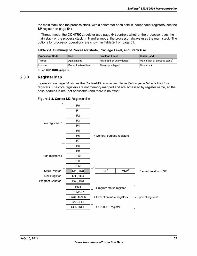
the main stack and the process stack, with a pointer for each held in independent registers (see theSP register on page 54).
In Thread mode, the CONTROL register (see page 64) controls whether the processor uses themain stack or the process stack. In Handler mode, the processor always uses the main stack. Theoptions for processor operations are shown in Table 2-1 on page 51.
Table 2-1. Summary of Processor Mode, Privilege Level, and Stack Use
Stack UsedPrivilege LevelUseProcessor Mode
Main stack or process stack aPrivileged or unprivileged aApplicationsThread
Main stackAlways privilegedException handlersHandler
a. See CONTROL (page 64).
2.3.3 Register MapFigure 2-3 on page 51 shows the Cortex-M3 register set. Table 2-2 on page 52 lists the Coreregisters. The core registers are not memory mapped and are accessed by register name, so thebase address is n/a (not applicable) and there is no offset.
Figure 2-3. Cortex-M3 Register Set
SP (R13)
LR (R14)
PC (R15)
R5
R6
R7
R0
R1
R3
R4
R2
R10
R11
R12
R8
R9
Low registers
High registers
MSP‡PSP‡
PSR
PRIMASK
FAULTMASK
BASEPRI
CONTROL
General-purpose registers
Stack Pointer
Link Register
Program Counter
Program status register
Exception mask registers
CONTROL register
Special registers
‡Banked version of SP
51July 16, 2014Texas Instruments-Production Data
Stellaris® LM3S2601 Microcontroller
Table 2-2. Processor Register Map
SeepageDescriptionResetTypeNameOffset
53Cortex General-Purpose Register 0-R/WR0-
53Cortex General-Purpose Register 1-R/WR1-
53Cortex General-Purpose Register 2-R/WR2-
53Cortex General-Purpose Register 3-R/WR3-
53Cortex General-Purpose Register 4-R/WR4-
53Cortex General-Purpose Register 5-R/WR5-
53Cortex General-Purpose Register 6-R/WR6-
53Cortex General-Purpose Register 7-R/WR7-
53Cortex General-Purpose Register 8-R/WR8-
53Cortex General-Purpose Register 9-R/WR9-
53Cortex General-Purpose Register 10-R/WR10-
53Cortex General-Purpose Register 11-R/WR11-
53Cortex General-Purpose Register 12-R/WR12-
54Stack Pointer-R/WSP-
55Link Register0xFFFF.FFFFR/WLR-
56Program Counter-R/WPC-
57Program Status Register0x0100.0000R/WPSR-
61Priority Mask Register0x0000.0000R/WPRIMASK-
62Fault Mask Register0x0000.0000R/WFAULTMASK-
63Base Priority Mask Register0x0000.0000R/WBASEPRI-
64Control Register0x0000.0000R/WCONTROL-
2.3.4 Register DescriptionsThis section lists and describes the Cortex-M3 registers, in the order shown in Figure 2-3 on page 51.The core registers are not memory mapped and are accessed by register name rather than offset.
Note: The register type shown in the register descriptions refers to type during program executionin Thread mode and Handler mode. Debug access can differ.
July 16, 201452Texas Instruments-Production Data
The Cortex-M3 Processor
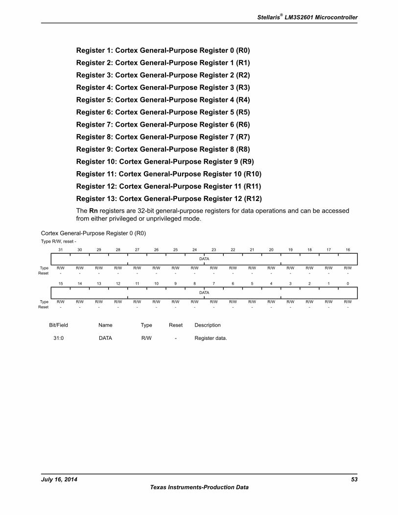
Register 1: Cortex General-Purpose Register 0 (R0)Register 2: Cortex General-Purpose Register 1 (R1)Register 3: Cortex General-Purpose Register 2 (R2)Register 4: Cortex General-Purpose Register 3 (R3)Register 5: Cortex General-Purpose Register 4 (R4)Register 6: Cortex General-Purpose Register 5 (R5)Register 7: Cortex General-Purpose Register 6 (R6)Register 8: Cortex General-Purpose Register 7 (R7)Register 9: Cortex General-Purpose Register 8 (R8)Register 10: Cortex General-Purpose Register 9 (R9)Register 11: Cortex General-Purpose Register 10 (R10)Register 12: Cortex General-Purpose Register 11 (R11)Register 13: Cortex General-Purpose Register 12 (R12)The Rn registers are 32-bit general-purpose registers for data operations and can be accessedfrom either privileged or unprivileged mode.
Cortex General-Purpose Register 0 (R0)Type R/W, reset -
16171819202122232425262728293031
DATA
R/WR/WR/WR/WR/WR/WR/WR/WR/WR/WR/WR/WR/WR/WR/WR/WType----------------Reset
0123456789101112131415
DATA
R/WR/WR/WR/WR/WR/WR/WR/WR/WR/WR/WR/WR/WR/WR/WR/WType----------------Reset
DescriptionResetTypeNameBit/Field
Register data.-R/WDATA31:0
53July 16, 2014Texas Instruments-Production Data
Stellaris® LM3S2601 Microcontroller
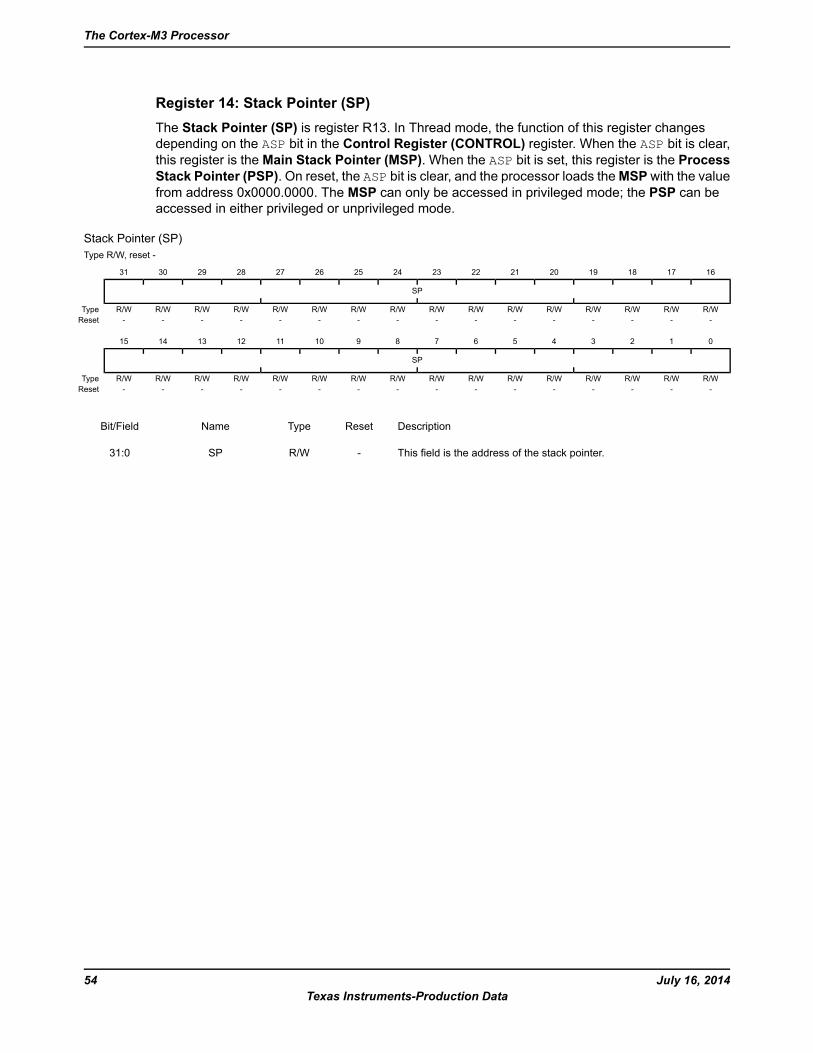
Register 14: Stack Pointer (SP)The Stack Pointer (SP) is register R13. In Thread mode, the function of this register changesdepending on the ASP bit in the Control Register (CONTROL) register. When the ASP bit is clear,this register is the Main Stack Pointer (MSP). When the ASP bit is set, this register is the ProcessStack Pointer (PSP). On reset, the ASP bit is clear, and the processor loads theMSP with the valuefrom address 0x0000.0000. The MSP can only be accessed in privileged mode; the PSP can beaccessed in either privileged or unprivileged mode.
Stack Pointer (SP)Type R/W, reset -
16171819202122232425262728293031
SP
R/WR/WR/WR/WR/WR/WR/WR/WR/WR/WR/WR/WR/WR/WR/WR/WType----------------Reset
0123456789101112131415
SP
R/WR/WR/WR/WR/WR/WR/WR/WR/WR/WR/WR/WR/WR/WR/WR/WType----------------Reset
DescriptionResetTypeNameBit/Field
This field is the address of the stack pointer.-R/WSP31:0
July 16, 201454Texas Instruments-Production Data
The Cortex-M3 Processor
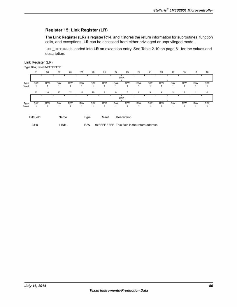
Register 15: Link Register (LR)The Link Register (LR) is register R14, and it stores the return information for subroutines, functioncalls, and exceptions. LR can be accessed from either privileged or unprivileged mode.
EXC_RETURN is loaded into LR on exception entry. See Table 2-10 on page 81 for the values anddescription.
Link Register (LR)Type R/W, reset 0xFFFF.FFFF
16171819202122232425262728293031
LINK
R/WR/WR/WR/WR/WR/WR/WR/WR/WR/WR/WR/WR/WR/WR/WR/WType1111111111111111Reset
0123456789101112131415
LINK
R/WR/WR/WR/WR/WR/WR/WR/WR/WR/WR/WR/WR/WR/WR/WR/WType1111111111111111Reset
DescriptionResetTypeNameBit/Field
This field is the return address.0xFFFF.FFFFR/WLINK31:0
55July 16, 2014Texas Instruments-Production Data
Stellaris® LM3S2601 Microcontroller
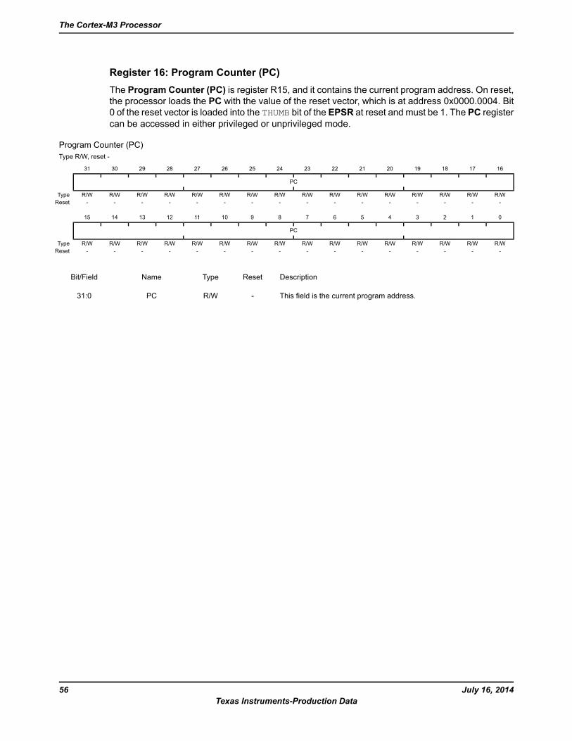
Register 16: Program Counter (PC)The Program Counter (PC) is register R15, and it contains the current program address. On reset,the processor loads the PC with the value of the reset vector, which is at address 0x0000.0004. Bit0 of the reset vector is loaded into the THUMB bit of the EPSR at reset and must be 1. The PC registercan be accessed in either privileged or unprivileged mode.
Program Counter (PC)Type R/W, reset -
16171819202122232425262728293031
PC
R/WR/WR/WR/WR/WR/WR/WR/WR/WR/WR/WR/WR/WR/WR/WR/WType----------------Reset
0123456789101112131415
PC
R/WR/WR/WR/WR/WR/WR/WR/WR/WR/WR/WR/WR/WR/WR/WR/WType----------------Reset
DescriptionResetTypeNameBit/Field
This field is the current program address.-R/WPC31:0
July 16, 201456Texas Instruments-Production Data
The Cortex-M3 Processor
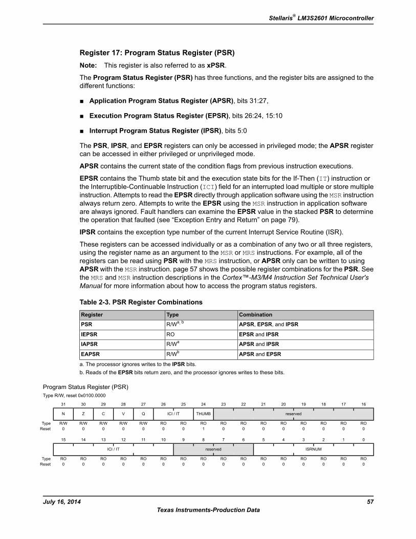
Register 17: Program Status Register (PSR)Note: This register is also referred to as xPSR.
The Program Status Register (PSR) has three functions, and the register bits are assigned to thedifferent functions:
Application Program Status Register (APSR), bits 31:27,
Execution Program Status Register (EPSR), bits 26:24, 15:10
Interrupt Program Status Register (IPSR), bits 5:0
The PSR, IPSR, and EPSR registers can only be accessed in privileged mode; the APSR registercan be accessed in either privileged or unprivileged mode.
APSR contains the current state of the condition flags from previous instruction executions.
EPSR contains the Thumb state bit and the execution state bits for the If-Then (IT) instruction orthe Interruptible-Continuable Instruction (ICI) field for an interrupted load multiple or store multipleinstruction. Attempts to read the EPSR directly through application software using the MSR instructionalways return zero. Attempts to write the EPSR using the MSR instruction in application softwareare always ignored. Fault handlers can examine the EPSR value in the stacked PSR to determinethe operation that faulted (see “Exception Entry and Return” on page 79).
IPSR contains the exception type number of the current Interrupt Service Routine (ISR).
These registers can be accessed individually or as a combination of any two or all three registers,using the register name as an argument to the MSR or MRS instructions. For example, all of theregisters can be read using PSR with the MRS instruction, or APSR only can be written to usingAPSR with the MSR instruction. page 57 shows the possible register combinations for the PSR. Seethe MRS and MSR instruction descriptions in the Cortex™-M3/M4 Instruction Set Technical User'sManual for more information about how to access the program status registers.
Table 2-3. PSR Register Combinations
CombinationTypeRegister
APSR, EPSR, and IPSRR/Wa, bPSR
EPSR and IPSRROIEPSR
APSR and IPSRR/WaIAPSR
APSR and EPSRR/WbEAPSR
a. The processor ignores writes to the IPSR bits.b. Reads of the EPSR bits return zero, and the processor ignores writes to these bits.
Program Status Register (PSR)Type R/W, reset 0x0100.0000
16171819202122232425262728293031
reservedTHUMBICI / ITQVCZN
ROROROROROROROROROROROR/WR/WR/WR/WR/WType0000000010000000Reset
0123456789101112131415
ISRNUMreservedICI / IT
ROROROROROROROROROROROROROROROROType0000000000000000Reset
57July 16, 2014Texas Instruments-Production Data
Stellaris® LM3S2601 Microcontroller
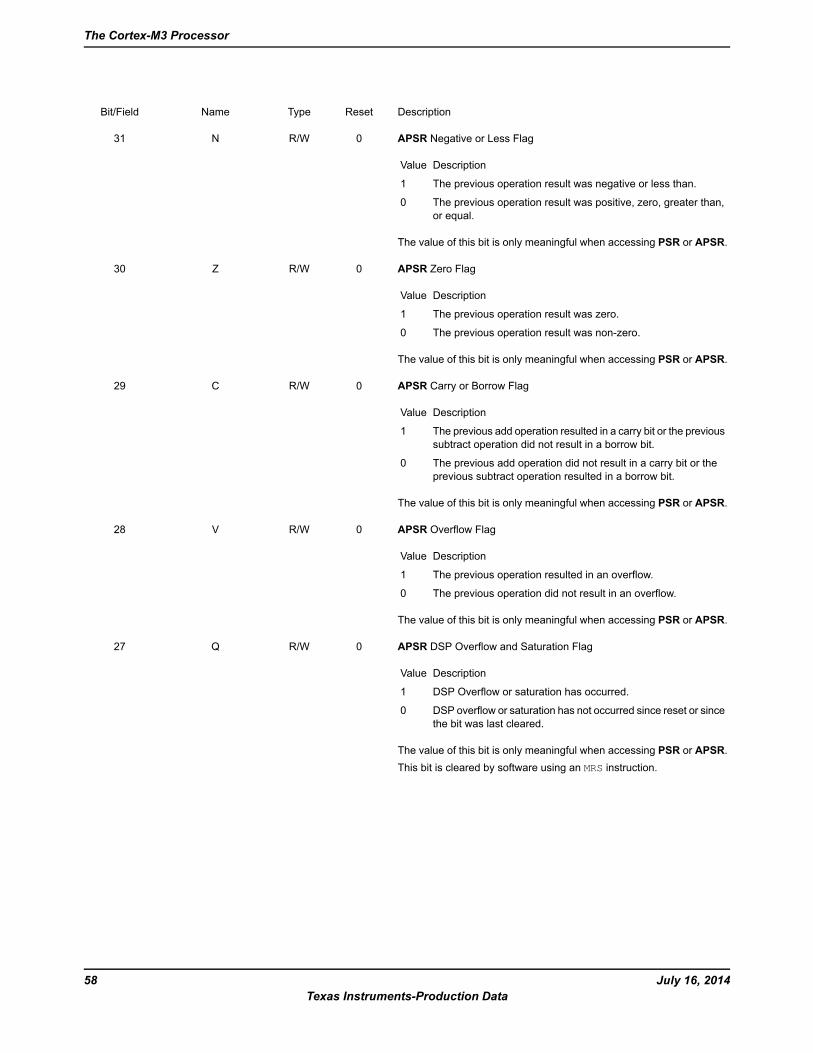
DescriptionResetTypeNameBit/Field
APSR Negative or Less Flag
DescriptionValue
The previous operation result was negative or less than.1
The previous operation result was positive, zero, greater than,or equal.
0
The value of this bit is only meaningful when accessing PSR or APSR.
0R/WN31
APSR Zero Flag
DescriptionValue
The previous operation result was zero.1
The previous operation result was non-zero.0
The value of this bit is only meaningful when accessing PSR or APSR.
0R/WZ30
APSR Carry or Borrow Flag
DescriptionValue
The previous add operation resulted in a carry bit or the previoussubtract operation did not result in a borrow bit.
1
The previous add operation did not result in a carry bit or theprevious subtract operation resulted in a borrow bit.
0
The value of this bit is only meaningful when accessing PSR or APSR.
0R/WC29
APSR Overflow Flag
DescriptionValue
The previous operation resulted in an overflow.1
The previous operation did not result in an overflow.0
The value of this bit is only meaningful when accessing PSR or APSR.
0R/WV28
APSR DSP Overflow and Saturation Flag
DescriptionValue
DSP Overflow or saturation has occurred.1
DSP overflow or saturation has not occurred since reset or sincethe bit was last cleared.
0
The value of this bit is only meaningful when accessing PSR or APSR.This bit is cleared by software using an MRS instruction.
0R/WQ27
July 16, 201458Texas Instruments-Production Data
The Cortex-M3 Processor
DescriptionResetTypeNameBit/Field
EPSR ICI / IT statusThese bits, along with bits 15:10, contain the Interruptible-ContinuableInstruction (ICI) field for an interrupted load multiple or store multipleinstruction or the execution state bits of the IT instruction.When EPSR holds the ICI execution state, bits 26:25 are zero.The If-Then block contains up to four instructions following an ITinstruction. Each instruction in the block is conditional. The conditionsfor the instructions are either all the same, or some can be the inverseof others. See the Cortex™-M3/M4 Instruction Set Technical User'sManual for more information.The value of this field is only meaningful when accessingPSR or EPSR.
0x0ROICI / IT26:25
EPSR Thumb StateThis bit indicates the Thumb state and should always be set.The following can clear the THUMB bit:
The BLX, BX and POPPC instructions
Restoration from the stacked xPSR value on an exception return
Bit 0 of the vector value on an exception entry or reset
Attempting to execute instructions when this bit is clear results in a faultor lockup. See “Lockup” on page 83 for more information.The value of this bit is only meaningful when accessing PSR or EPSR.
1ROTHUMB24
Software should not rely on the value of a reserved bit. To providecompatibility with future products, the value of a reserved bit should bepreserved across a read-modify-write operation.
0x00ROreserved23:16
EPSR ICI / IT statusThese bits, along with bits 26:25, contain the Interruptible-ContinuableInstruction (ICI) field for an interrupted load multiple or store multipleinstruction or the execution state bits of the IT instruction.When an interrupt occurs during the execution of an LDM, STM, PUSHor POP instruction, the processor stops the load multiple or store multipleinstruction operation temporarily and stores the next register operandin the multiple operation to bits 15:12. After servicing the interrupt, theprocessor returns to the register pointed to by bits 15:12 and resumesexecution of the multiple load or store instruction. When EPSR holdsthe ICI execution state, bits 11:10 are zero.The If-Then block contains up to four instructions following a 16-bit ITinstruction. Each instruction in the block is conditional. The conditionsfor the instructions are either all the same, or some can be the inverseof others. See the Cortex™-M3/M4 Instruction Set Technical User'sManual for more information.The value of this field is only meaningful when accessingPSR or EPSR.
0x0ROICI / IT15:10
Software should not rely on the value of a reserved bit. To providecompatibility with future products, the value of a reserved bit should bepreserved across a read-modify-write operation.
0x0ROreserved9:6
59July 16, 2014Texas Instruments-Production Data
Stellaris® LM3S2601 Microcontroller
DescriptionResetTypeNameBit/Field
IPSR ISR NumberThis field contains the exception type number of the current InterruptService Routine (ISR).
DescriptionValue
Thread mode0x00
Reserved0x01
NMI0x02
Hard fault0x03
Memory management fault0x04
Bus fault0x05
Usage fault0x06
Reserved0x07-0x0A
SVCall0x0B
Reserved for Debug0x0C
Reserved0x0D
PendSV0x0E
SysTick0x0F
Interrupt Vector 00x10
Interrupt Vector 10x11
......
Interrupt Vector 430x3B
Reserved0x3C-0x3F
See “Exception Types” on page 74 for more information.The value of this field is only meaningful when accessing PSR or IPSR.
0x00ROISRNUM5:0
July 16, 201460Texas Instruments-Production Data
The Cortex-M3 Processor
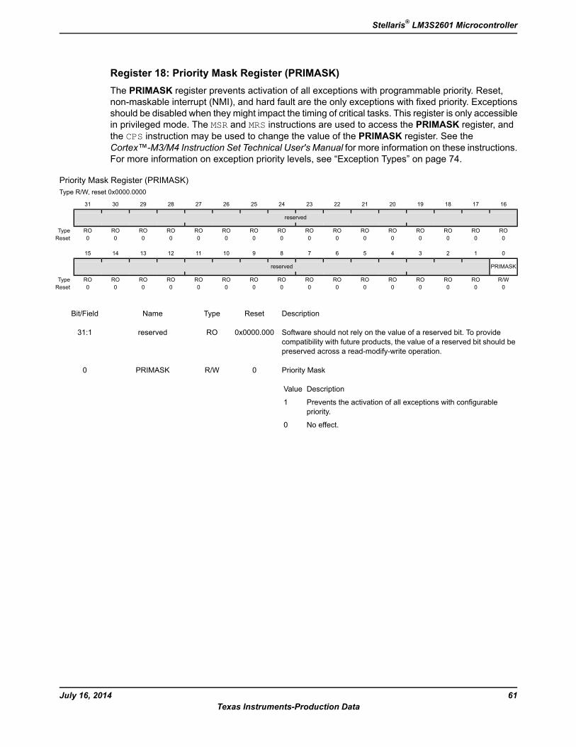
Register 18: Priority Mask Register (PRIMASK)The PRIMASK register prevents activation of all exceptions with programmable priority. Reset,non-maskable interrupt (NMI), and hard fault are the only exceptions with fixed priority. Exceptionsshould be disabled when they might impact the timing of critical tasks. This register is only accessiblein privileged mode. The MSR and MRS instructions are used to access the PRIMASK register, andthe CPS instruction may be used to change the value of the PRIMASK register. See theCortex™-M3/M4 Instruction Set Technical User's Manual for more information on these instructions.For more information on exception priority levels, see “Exception Types” on page 74.
Priority Mask Register (PRIMASK)Type R/W, reset 0x0000.0000
16171819202122232425262728293031
reserved
ROROROROROROROROROROROROROROROROType0000000000000000Reset
0123456789101112131415
PRIMASKreserved
R/WROROROROROROROROROROROROROROROType0000000000000000Reset
DescriptionResetTypeNameBit/Field
Software should not rely on the value of a reserved bit. To providecompatibility with future products, the value of a reserved bit should bepreserved across a read-modify-write operation.
0x0000.000ROreserved31:1
Priority Mask
DescriptionValue
Prevents the activation of all exceptions with configurablepriority.
1
No effect.0
0R/WPRIMASK0
61July 16, 2014Texas Instruments-Production Data
Stellaris® LM3S2601 Microcontroller
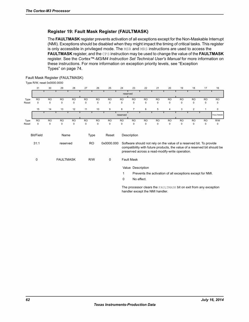
Register 19: Fault Mask Register (FAULTMASK)The FAULTMASK register prevents activation of all exceptions except for the Non-Maskable Interrupt(NMI). Exceptions should be disabled when they might impact the timing of critical tasks. This registeris only accessible in privileged mode. The MSR and MRS instructions are used to access theFAULTMASK register, and the CPS instruction may be used to change the value of the FAULTMASKregister. See the Cortex™-M3/M4 Instruction Set Technical User's Manual for more information onthese instructions. For more information on exception priority levels, see “ExceptionTypes” on page 74.
Fault Mask Register (FAULTMASK)Type R/W, reset 0x0000.0000
16171819202122232425262728293031
reserved
ROROROROROROROROROROROROROROROROType0000000000000000Reset
0123456789101112131415
FAULTMASKreserved
R/WROROROROROROROROROROROROROROROType0000000000000000Reset
DescriptionResetTypeNameBit/Field
Software should not rely on the value of a reserved bit. To providecompatibility with future products, the value of a reserved bit should bepreserved across a read-modify-write operation.
0x0000.000ROreserved31:1
Fault Mask
DescriptionValue
Prevents the activation of all exceptions except for NMI.1
No effect.0
The processor clears the FAULTMASK bit on exit from any exceptionhandler except the NMI handler.
0R/WFAULTMASK0
July 16, 201462Texas Instruments-Production Data
The Cortex-M3 Processor
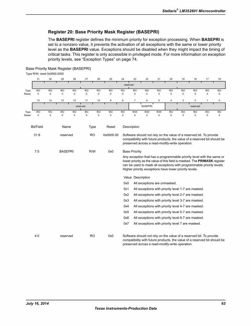
Register 20: Base Priority Mask Register (BASEPRI)The BASEPRI register defines the minimum priority for exception processing. When BASEPRI isset to a nonzero value, it prevents the activation of all exceptions with the same or lower prioritylevel as the BASEPRI value. Exceptions should be disabled when they might impact the timing ofcritical tasks. This register is only accessible in privileged mode. For more information on exceptionpriority levels, see “Exception Types” on page 74.
Base Priority Mask Register (BASEPRI)Type R/W, reset 0x0000.0000
16171819202122232425262728293031
reserved
ROROROROROROROROROROROROROROROROType0000000000000000Reset
0123456789101112131415
reservedBASEPRIreserved
ROROROROROR/WR/WR/WROROROROROROROROType0000000000000000Reset
DescriptionResetTypeNameBit/Field
Software should not rely on the value of a reserved bit. To providecompatibility with future products, the value of a reserved bit should bepreserved across a read-modify-write operation.
0x0000.00ROreserved31:8
Base PriorityAny exception that has a programmable priority level with the same orlower priority as the value of this field is masked. The PRIMASK registercan be used to mask all exceptions with programmable priority levels.Higher priority exceptions have lower priority levels.
DescriptionValue
All exceptions are unmasked.0x0
All exceptions with priority level 1-7 are masked.0x1
All exceptions with priority level 2-7 are masked.0x2
All exceptions with priority level 3-7 are masked.0x3
All exceptions with priority level 4-7 are masked.0x4
All exceptions with priority level 5-7 are masked.0x5
All exceptions with priority level 6-7 are masked.0x6
All exceptions with priority level 7 are masked.0x7
0x0R/WBASEPRI7:5
Software should not rely on the value of a reserved bit. To providecompatibility with future products, the value of a reserved bit should bepreserved across a read-modify-write operation.
0x0ROreserved4:0
63July 16, 2014Texas Instruments-Production Data
Stellaris® LM3S2601 Microcontroller
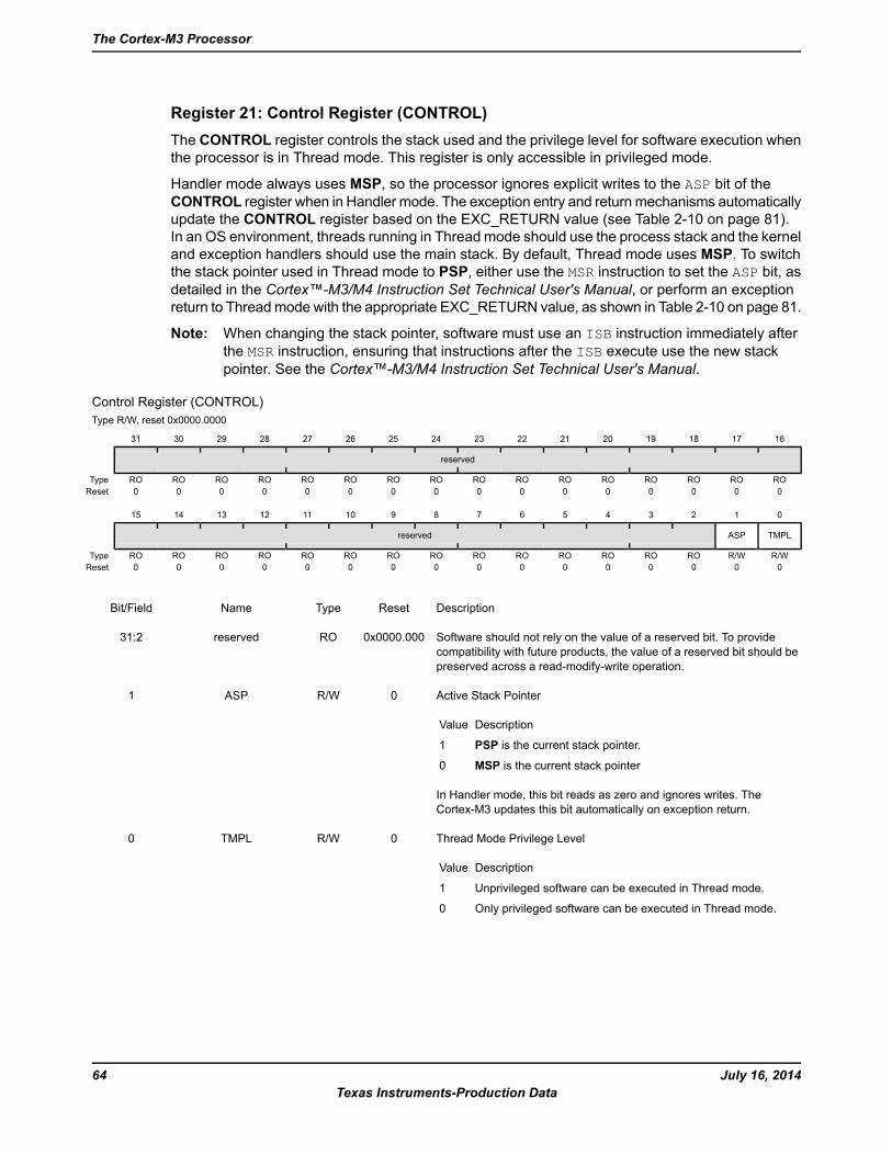
Register 21: Control Register (CONTROL)The CONTROL register controls the stack used and the privilege level for software execution whenthe processor is in Thread mode. This register is only accessible in privileged mode.
Handler mode always uses MSP, so the processor ignores explicit writes to the ASP bit of theCONTROL register when in Handler mode. The exception entry and returnmechanisms automaticallyupdate the CONTROL register based on the EXC_RETURN value (see Table 2-10 on page 81).In an OS environment, threads running in Thread mode should use the process stack and the kerneland exception handlers should use the main stack. By default, Thread mode uses MSP. To switchthe stack pointer used in Thread mode to PSP, either use the MSR instruction to set the ASP bit, asdetailed in the Cortex™-M3/M4 Instruction Set Technical User's Manual, or perform an exceptionreturn to Threadmode with the appropriate EXC_RETURN value, as shown in Table 2-10 on page 81.
Note: When changing the stack pointer, software must use an ISB instruction immediately afterthe MSR instruction, ensuring that instructions after the ISB execute use the new stackpointer. See the Cortex™-M3/M4 Instruction Set Technical User's Manual.
Control Register (CONTROL)Type R/W, reset 0x0000.0000
16171819202122232425262728293031
reserved
ROROROROROROROROROROROROROROROROType0000000000000000Reset
0123456789101112131415
TMPLASPreserved
R/WR/WROROROROROROROROROROROROROROType0000000000000000Reset
DescriptionResetTypeNameBit/Field
Software should not rely on the value of a reserved bit. To providecompatibility with future products, the value of a reserved bit should bepreserved across a read-modify-write operation.
0x0000.000ROreserved31:2
Active Stack Pointer
DescriptionValue
PSP is the current stack pointer.1
MSP is the current stack pointer0
In Handler mode, this bit reads as zero and ignores writes. TheCortex-M3 updates this bit automatically on exception return.
0R/WASP1
Thread Mode Privilege Level
DescriptionValue
Unprivileged software can be executed in Thread mode.1
Only privileged software can be executed in Thread mode.0
0R/WTMPL0
July 16, 201464Texas Instruments-Production Data
The Cortex-M3 Processor
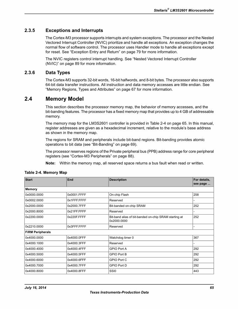
2.3.5 Exceptions and InterruptsThe Cortex-M3 processor supports interrupts and system exceptions. The processor and the NestedVectored Interrupt Controller (NVIC) prioritize and handle all exceptions. An exception changes thenormal flow of software control. The processor uses Handler mode to handle all exceptions exceptfor reset. See “Exception Entry and Return” on page 79 for more information.
The NVIC registers control interrupt handling. See “Nested Vectored Interrupt Controller(NVIC)” on page 89 for more information.
2.3.6 Data TypesThe Cortex-M3 supports 32-bit words, 16-bit halfwords, and 8-bit bytes. The processor also supports64-bit data transfer instructions. All instruction and data memory accesses are little endian. See“Memory Regions, Types and Attributes” on page 67 for more information.
2.4 Memory ModelThis section describes the processor memory map, the behavior of memory accesses, and thebit-banding features. The processor has a fixed memory map that provides up to 4 GB of addressablememory.
The memory map for the LM3S2601 controller is provided in Table 2-4 on page 65. In this manual,register addresses are given as a hexadecimal increment, relative to the module’s base addressas shown in the memory map.
The regions for SRAM and peripherals include bit-band regions. Bit-banding provides atomicoperations to bit data (see “Bit-Banding” on page 69).
The processor reserves regions of the Private peripheral bus (PPB) address range for core peripheralregisters (see “Cortex-M3 Peripherals” on page 88).
Note: Within the memory map, all reserved space returns a bus fault when read or written.
Table 2-4. Memory Map
For details,see page ...
DescriptionEndStart
Memory
258On-chip Flash0x0001.FFFF0x0000.0000
-Reserved0x1FFF.FFFF0x0002.0000
252Bit-banded on-chip SRAM0x2000.7FFF0x2000.0000
-Reserved0x21FF.FFFF0x2000.8000
252Bit-band alias of bit-banded on-chip SRAM starting at0x2000.0000
0x220F.FFFF0x2200.0000
-Reserved0x3FFF.FFFF0x2210.0000
FiRM Peripherals
367Watchdog timer 00x4000.0FFF0x4000.0000
-Reserved0x4000.3FFF0x4000.1000
292GPIO Port A0x4000.4FFF0x4000.4000
292GPIO Port B0x4000.5FFF0x4000.5000
292GPIO Port C0x4000.6FFF0x4000.6000
292GPIO Port D0x4000.7FFF0x4000.7000
443SSI00x4000.8FFF0x4000.8000
65July 16, 2014Texas Instruments-Production Data
Stellaris® LM3S2601 Microcontroller
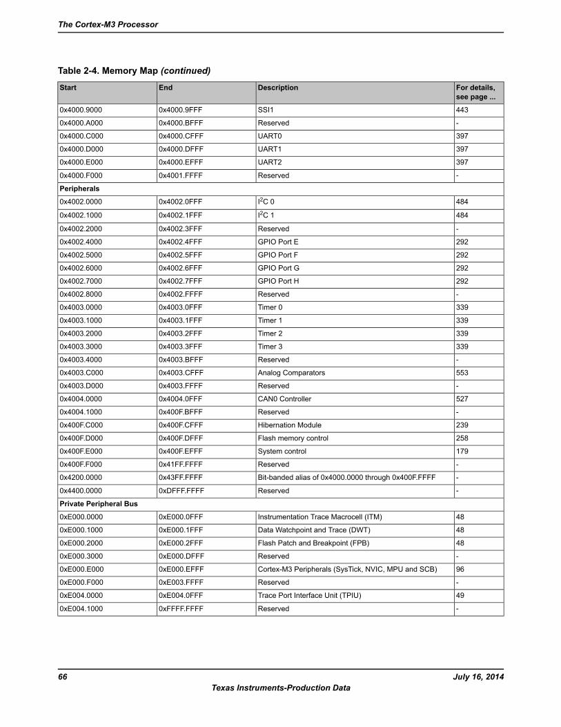
Table 2-4. Memory Map (continued)
For details,see page ...
DescriptionEndStart
443SSI10x4000.9FFF0x4000.9000
-Reserved0x4000.BFFF0x4000.A000
397UART00x4000.CFFF0x4000.C000
397UART10x4000.DFFF0x4000.D000
397UART20x4000.EFFF0x4000.E000
-Reserved0x4001.FFFF0x4000.F000
Peripherals
484I2C 00x4002.0FFF0x4002.0000
484I2C 10x4002.1FFF0x4002.1000
-Reserved0x4002.3FFF0x4002.2000
292GPIO Port E0x4002.4FFF0x4002.4000
292GPIO Port F0x4002.5FFF0x4002.5000
292GPIO Port G0x4002.6FFF0x4002.6000
292GPIO Port H0x4002.7FFF0x4002.7000
-Reserved0x4002.FFFF0x4002.8000
339Timer 00x4003.0FFF0x4003.0000
339Timer 10x4003.1FFF0x4003.1000
339Timer 20x4003.2FFF0x4003.2000
339Timer 30x4003.3FFF0x4003.3000
-Reserved0x4003.BFFF0x4003.4000
553Analog Comparators0x4003.CFFF0x4003.C000
-Reserved0x4003.FFFF0x4003.D000
527CAN0 Controller0x4004.0FFF0x4004.0000
-Reserved0x400F.BFFF0x4004.1000
239Hibernation Module0x400F.CFFF0x400F.C000
258Flash memory control0x400F.DFFF0x400F.D000
179System control0x400F.EFFF0x400F.E000
-Reserved0x41FF.FFFF0x400F.F000
-Bit-banded alias of 0x4000.0000 through 0x400F.FFFF0x43FF.FFFF0x4200.0000
-Reserved0xDFFF.FFFF0x4400.0000
Private Peripheral Bus
48Instrumentation Trace Macrocell (ITM)0xE000.0FFF0xE000.0000
48Data Watchpoint and Trace (DWT)0xE000.1FFF0xE000.1000
48Flash Patch and Breakpoint (FPB)0xE000.2FFF0xE000.2000
-Reserved0xE000.DFFF0xE000.3000
96Cortex-M3 Peripherals (SysTick, NVIC, MPU and SCB)0xE000.EFFF0xE000.E000
-Reserved0xE003.FFFF0xE000.F000
49Trace Port Interface Unit (TPIU)0xE004.0FFF0xE004.0000
-Reserved0xFFFF.FFFF0xE004.1000
July 16, 201466Texas Instruments-Production Data
The Cortex-M3 Processor
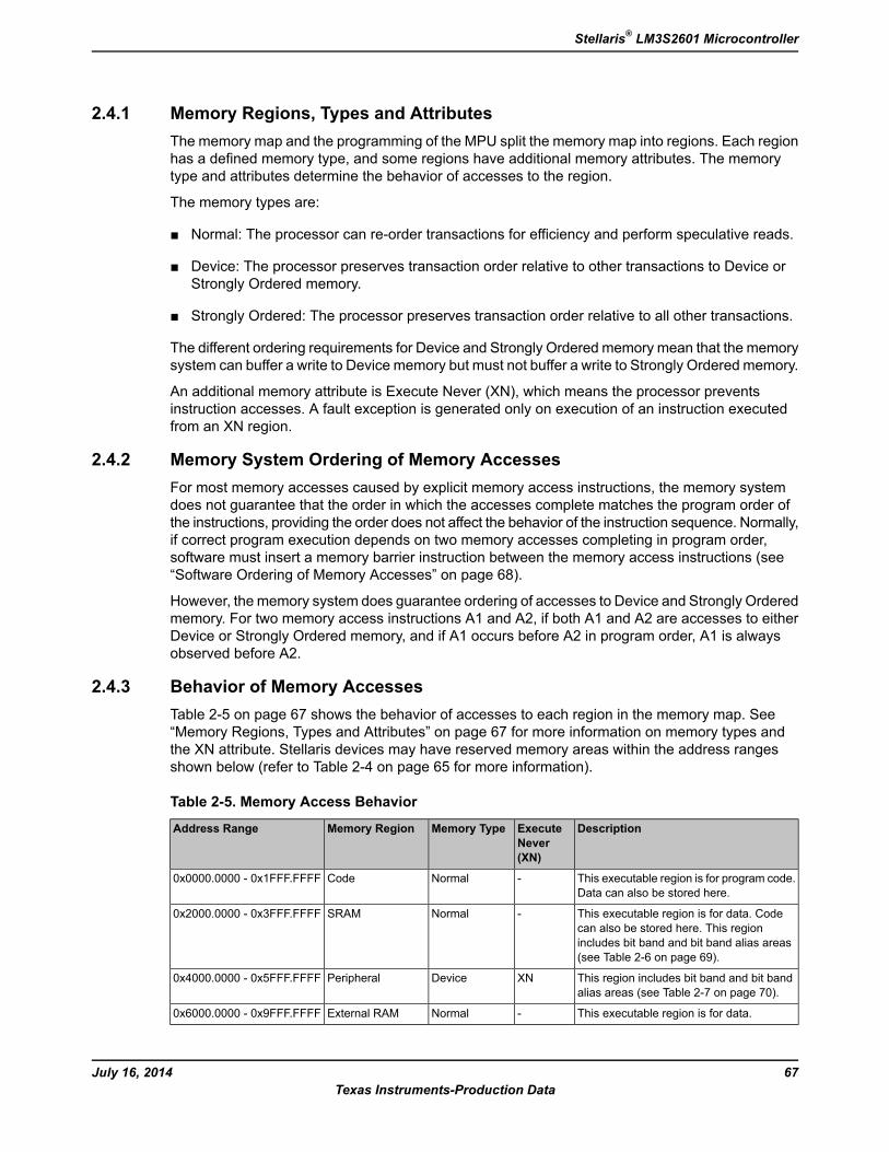
2.4.1 Memory Regions, Types and AttributesThe memory map and the programming of the MPU split the memory map into regions. Each regionhas a defined memory type, and some regions have additional memory attributes. The memorytype and attributes determine the behavior of accesses to the region.
The memory types are:
Normal: The processor can re-order transactions for efficiency and perform speculative reads.
Device: The processor preserves transaction order relative to other transactions to Device orStrongly Ordered memory.
Strongly Ordered: The processor preserves transaction order relative to all other transactions.
The different ordering requirements for Device and Strongly Ordered memory mean that the memorysystem can buffer a write to Device memory but must not buffer a write to Strongly Ordered memory.
An additional memory attribute is Execute Never (XN), which means the processor preventsinstruction accesses. A fault exception is generated only on execution of an instruction executedfrom an XN region.
2.4.2 Memory System Ordering of Memory AccessesFor most memory accesses caused by explicit memory access instructions, the memory systemdoes not guarantee that the order in which the accesses complete matches the program order ofthe instructions, providing the order does not affect the behavior of the instruction sequence. Normally,if correct program execution depends on two memory accesses completing in program order,software must insert a memory barrier instruction between the memory access instructions (see“Software Ordering of Memory Accesses” on page 68).
However, the memory system does guarantee ordering of accesses to Device and Strongly Orderedmemory. For two memory access instructions A1 and A2, if both A1 and A2 are accesses to eitherDevice or Strongly Ordered memory, and if A1 occurs before A2 in program order, A1 is alwaysobserved before A2.
2.4.3 Behavior of Memory AccessesTable 2-5 on page 67 shows the behavior of accesses to each region in the memory map. See“Memory Regions, Types and Attributes” on page 67 for more information on memory types andthe XN attribute. Stellaris devices may have reserved memory areas within the address rangesshown below (refer to Table 2-4 on page 65 for more information).
Table 2-5. Memory Access Behavior
DescriptionExecuteNever(XN)
Memory TypeMemory RegionAddress Range
This executable region is for program code.Data can also be stored here.
-NormalCode0x0000.0000 - 0x1FFF.FFFF
This executable region is for data. Codecan also be stored here. This regionincludes bit band and bit band alias areas(see Table 2-6 on page 69).
-NormalSRAM0x2000.0000 - 0x3FFF.FFFF
This region includes bit band and bit bandalias areas (see Table 2-7 on page 70).
XNDevicePeripheral0x4000.0000 - 0x5FFF.FFFF
This executable region is for data.-NormalExternal RAM0x6000.0000 - 0x9FFF.FFFF
67July 16, 2014Texas Instruments-Production Data
Stellaris® LM3S2601 Microcontroller
Table 2-5. Memory Access Behavior (continued)
DescriptionExecuteNever(XN)
Memory TypeMemory RegionAddress Range
This region is for external device memory.XNDeviceExternal device0xA000.0000 - 0xDFFF.FFFF
This region includes the NVIC, systemtimer, and system control block.
XNStronglyOrdered
Private peripheralbus
0xE000.0000- 0xE00F.FFFF
---Reserved0xE010.0000- 0xFFFF.FFFF
The Code, SRAM, and external RAM regions can hold programs. However, it is recommended thatprograms always use the Code region because the Cortex-M3 has separate buses that can performinstruction fetches and data accesses simultaneously.
The MPU can override the default memory access behavior described in this section. For moreinformation, see “Memory Protection Unit (MPU)” on page 91.
The Cortex-M3 prefetches instructions ahead of execution and speculatively prefetches from branchtarget addresses.
2.4.4 Software Ordering of Memory AccessesThe order of instructions in the program flow does not always guarantee the order of thecorresponding memory transactions for the following reasons:
The processor can reorder some memory accesses to improve efficiency, providing this doesnot affect the behavior of the instruction sequence.
The processor has multiple bus interfaces.
Memory or devices in the memory map have different wait states.
Some memory accesses are buffered or speculative.
“Memory SystemOrdering of Memory Accesses” on page 67 describes the cases where the memorysystem guarantees the order of memory accesses. Otherwise, if the order of memory accesses iscritical, software must include memory barrier instructions to force that ordering. The Cortex-M3has the following memory barrier instructions:
The Data Memory Barrier (DMB) instruction ensures that outstanding memory transactionscomplete before subsequent memory transactions.
The Data Synchronization Barrier (DSB) instruction ensures that outstanding memory transactionscomplete before subsequent instructions execute.
The Instruction Synchronization Barrier (ISB) instruction ensures that the effect of all completedmemory transactions is recognizable by subsequent instructions.
Memory barrier instructions can be used in the following situations:
MPU programming
– If the MPU settings are changed and the change must be effective on the very next instruction,use a DSB instruction to ensure the effect of the MPU takes place immediately at the end ofcontext switching.
July 16, 201468Texas Instruments-Production Data
The Cortex-M3 Processor
– Use an ISB instruction to ensure the new MPU setting takes effect immediately afterprogramming the MPU region or regions, if the MPU configuration code was accessed usinga branch or call. If the MPU configuration code is entered using exception mechanisms, thenan ISB instruction is not required.
Vector table
If the program changes an entry in the vector table and then enables the corresponding exception,use a DMB instruction between the operations. The DMB instruction ensures that if the exceptionis taken immediately after being enabled, the processor uses the new exception vector.
Self-modifying code
If a program contains self-modifying code, use an ISB instruction immediately after the codemodification in the program. The ISB instruction ensures subsequent instruction execution usesthe updated program.
Memory map switching
If the system contains a memory map switching mechanism, use a DSB instruction after switchingthe memory map in the program. The DSB instruction ensures subsequent instruction executionuses the updated memory map.
Dynamic exception priority change
When an exception priority has to change when the exception is pending or active, use DSBinstructions after the change. The change then takes effect on completion of the DSB instruction.
Memory accesses to Strongly Ordered memory, such as the System Control Block, do not requirethe use of DMB instructions.
For more information on the memory barrier instructions, see the Cortex™-M3/M4 Instruction SetTechnical User's Manual.
2.4.5 Bit-BandingA bit-band region maps each word in a bit-band alias region to a single bit in the bit-band region.The bit-band regions occupy the lowest 1 MB of the SRAM and peripheral memory regions. Accessesto the 32-MB SRAM alias region map to the 1-MB SRAM bit-band region, as shown in Table2-6 on page 69. Accesses to the 32-MB peripheral alias region map to the 1-MB peripheral bit-bandregion, as shown in Table 2-7 on page 70. For the specific address range of the bit-band regions,see Table 2-4 on page 65.
Note: A word access to the SRAM or the peripheral bit-band alias region maps to a single bit inthe SRAM or peripheral bit-band region.
A word access to a bit band address results in a word access to the underlying memory,and similarly for halfword and byte accesses. This allows bit band accesses to match theaccess requirements of the underlying peripheral.
Table 2-6. SRAM Memory Bit-Banding Regions
Instruction and Data AccessesMemory RegionAddress Range
EndStart
Direct accesses to this memory range behave as SRAMmemory accesses, but this region is also bit addressablethrough bit-band alias.
SRAM bit-band region0x2000.7FFF0x2000.0000
69July 16, 2014Texas Instruments-Production Data
Stellaris® LM3S2601 Microcontroller
Table 2-6. SRAM Memory Bit-Banding Regions (continued)
Instruction and Data AccessesMemory RegionAddress Range
EndStart
Data accesses to this region are remapped to bit bandregion. A write operation is performed asread-modify-write. Instruction accesses are not remapped.
SRAM bit-band alias0x220F.FFFF0x2200.0000
Table 2-7. Peripheral Memory Bit-Banding Regions
Instruction and Data AccessesMemory RegionAddress Range
EndStart
Direct accesses to this memory range behave asperipheral memory accesses, but this region is also bitaddressable through bit-band alias.
Peripheral bit-bandregion
0x400F.FFFF0x4000.0000
Data accesses to this region are remapped to bit bandregion. A write operation is performed asread-modify-write. Instruction accesses are not permitted.
Peripheral bit-band alias0x43FF.FFFF0x4200.0000
The following formula shows how the alias region maps onto the bit-band region:
bit_word_offset = (byte_offset x 32) + (bit_number x 4)
bit_word_addr = bit_band_base + bit_word_offset
where:
bit_word_offsetThe position of the target bit in the bit-band memory region.
bit_word_addrThe address of the word in the alias memory region that maps to the targeted bit.
bit_band_baseThe starting address of the alias region.
byte_offsetThe number of the byte in the bit-band region that contains the targeted bit.
bit_numberThe bit position, 0-7, of the targeted bit.
Figure 2-4 on page 71 shows examples of bit-band mapping between the SRAM bit-band aliasregion and the SRAM bit-band region:
The alias word at 0x23FF.FFE0 maps to bit 0 of the bit-band byte at 0x200F.FFFF:
0x23FF.FFE0 = 0x2200.0000 + (0x000F.FFFF*32) + (0*4)
The alias word at 0x23FF.FFFC maps to bit 7 of the bit-band byte at 0x200F.FFFF:
0x23FF.FFFC = 0x2200.0000 + (0x000F.FFFF*32) + (7*4)
The alias word at 0x2200.0000 maps to bit 0 of the bit-band byte at 0x2000.0000:
July 16, 201470Texas Instruments-Production Data
The Cortex-M3 Processor
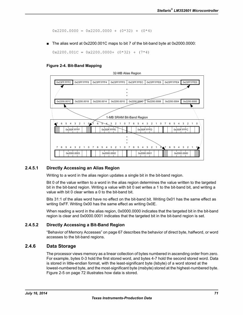
0x2200.0000 = 0x2200.0000 + (0*32) + (0*4)
The alias word at 0x2200.001C maps to bit 7 of the bit-band byte at 0x2000.0000:
0x2200.001C = 0x2200.0000+ (0*32) + (7*4)
Figure 2-4. Bit-Band Mapping
0x23FF.FFE4
0x2200.0004
0x23FF.FFE00x23FF.FFE80x23FF.FFEC0x23FF.FFF00x23FF.FFF40x23FF.FFF80x23FF.FFFC
0x2200.00000x2200.00140x2200.00180x2200.001C 0x2200.00080x2200.0010 0x2200.000C
32-MB Alias Region
0
7 0
07
0x2000.00000x2000.00010x2000.00020x2000.0003
6 5 4 3 2 1 07 6 5 4 3 2 1 7 6 5 4 3 2 1 07 6 5 4 3 2 1
07 6 5 4 3 2 1 6 5 4 3 2 107 6 5 4 3 2 1 07 6 5 4 3 2 1
0x200F.FFFC0x200F.FFFD0x200F.FFFE0x200F.FFFF
1-MB SRAM Bit-Band Region
2.4.5.1 Directly Accessing an Alias RegionWriting to a word in the alias region updates a single bit in the bit-band region.
Bit 0 of the value written to a word in the alias region determines the value written to the targetedbit in the bit-band region. Writing a value with bit 0 set writes a 1 to the bit-band bit, and writing avalue with bit 0 clear writes a 0 to the bit-band bit.
Bits 31:1 of the alias word have no effect on the bit-band bit. Writing 0x01 has the same effect aswriting 0xFF. Writing 0x00 has the same effect as writing 0x0E.
When reading a word in the alias region, 0x0000.0000 indicates that the targeted bit in the bit-bandregion is clear and 0x0000.0001 indicates that the targeted bit in the bit-band region is set.
2.4.5.2 Directly Accessing a Bit-Band Region“Behavior of Memory Accesses” on page 67 describes the behavior of direct byte, halfword, or wordaccesses to the bit-band regions.
2.4.6 Data StorageThe processor views memory as a linear collection of bytes numbered in ascending order from zero.For example, bytes 0-3 hold the first stored word, and bytes 4-7 hold the second stored word. Datais stored in little-endian format, with the least-significant byte (lsbyte) of a word stored at thelowest-numbered byte, and the most-significant byte (msbyte) stored at the highest-numbered byte.Figure 2-5 on page 72 illustrates how data is stored.
71July 16, 2014Texas Instruments-Production Data
Stellaris® LM3S2601 Microcontroller
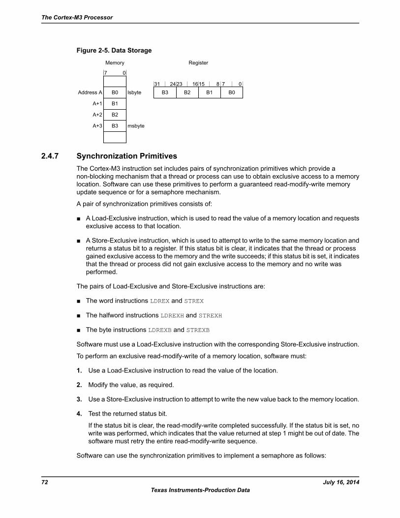
Figure 2-5. Data Storage
Memory Register
Address A
A+1
lsbyte
msbyte
A+2
A+3
07
B0B1B3 B231 2423 1615 8 7 0
B0
B1
B2
B3
2.4.7 Synchronization PrimitivesThe Cortex-M3 instruction set includes pairs of synchronization primitives which provide anon-blocking mechanism that a thread or process can use to obtain exclusive access to a memorylocation. Software can use these primitives to perform a guaranteed read-modify-write memoryupdate sequence or for a semaphore mechanism.
A pair of synchronization primitives consists of:
A Load-Exclusive instruction, which is used to read the value of a memory location and requestsexclusive access to that location.
A Store-Exclusive instruction, which is used to attempt to write to the same memory location andreturns a status bit to a register. If this status bit is clear, it indicates that the thread or processgained exclusive access to the memory and the write succeeds; if this status bit is set, it indicatesthat the thread or process did not gain exclusive access to the memory and no write wasperformed.
The pairs of Load-Exclusive and Store-Exclusive instructions are:
The word instructions LDREX and STREX
The halfword instructions LDREXH and STREXH
The byte instructions LDREXB and STREXB
Software must use a Load-Exclusive instruction with the corresponding Store-Exclusive instruction.
To perform an exclusive read-modify-write of a memory location, software must:
1. Use a Load-Exclusive instruction to read the value of the location.
2. Modify the value, as required.
3. Use a Store-Exclusive instruction to attempt to write the new value back to the memory location.
4. Test the returned status bit.
If the status bit is clear, the read-modify-write completed successfully. If the status bit is set, nowrite was performed, which indicates that the value returned at step 1 might be out of date. Thesoftware must retry the entire read-modify-write sequence.
Software can use the synchronization primitives to implement a semaphore as follows:
July 16, 201472Texas Instruments-Production Data
The Cortex-M3 Processor
1. Use a Load-Exclusive instruction to read from the semaphore address to check whether thesemaphore is free.
2. If the semaphore is free, use a Store-Exclusive to write the claim value to the semaphoreaddress.
3. If the returned status bit from step 2 indicates that the Store-Exclusive succeeded, then thesoftware has claimed the semaphore. However, if the Store-Exclusive failed, another processmight have claimed the semaphore after the software performed step 1.
The Cortex-M3 includes an exclusive access monitor that tags the fact that the processor hasexecuted a Load-Exclusive instruction. The processor removes its exclusive access tag if:
It executes a CLREX instruction.
It executes a Store-Exclusive instruction, regardless of whether the write succeeds.
An exception occurs, which means the processor can resolve semaphore conflicts betweendifferent threads.
For more information about the synchronization primitive instructions, see the Cortex™-M3/M4Instruction Set Technical User's Manual.
2.5 Exception ModelThe ARM Cortex-M3 processor and the Nested Vectored Interrupt Controller (NVIC) prioritize andhandle all exceptions in Handler Mode. The processor state is automatically stored to the stack onan exception and automatically restored from the stack at the end of the Interrupt Service Routine(ISR). The vector is fetched in parallel to the state saving, enabling efficient interrupt entry. Theprocessor supports tail-chaining, which enables back-to-back interrupts to be performed without theoverhead of state saving and restoration.
Table 2-8 on page 75 lists all exception types. Software can set eight priority levels on seven ofthese exceptions (system handlers) as well as on 30 interrupts (listed in Table 2-9 on page 76).
Priorities on the system handlers are set with the NVIC System Handler Priority n (SYSPRIn)registers. Interrupts are enabled through the NVIC Interrupt Set Enable n (ENn) register andprioritized with the NVIC Interrupt Priority n (PRIn) registers. Priorities can be grouped by splittingpriority levels into preemption priorities and subpriorities. All the interrupt registers are described in“Nested Vectored Interrupt Controller (NVIC)” on page 89.
Internally, the highest user-programmable priority (0) is treated as fourth priority, after a Reset,Non-Maskable Interrupt (NMI), and a Hard Fault, in that order. Note that 0 is the default priority forall the programmable priorities.
Important: After a write to clear an interrupt source, it may take several processor cycles for theNVIC to see the interrupt source de-assert. Thus if the interrupt clear is done as thelast action in an interrupt handler, it is possible for the interrupt handler to completewhile the NVIC sees the interrupt as still asserted, causing the interrupt handler to bere-entered errantly. This situation can be avoided by either clearing the interrupt sourceat the beginning of the interrupt handler or by performing a read or write after the writeto clear the interrupt source (and flush the write buffer).
See “Nested Vectored Interrupt Controller (NVIC)” on page 89 for more information on exceptionsand interrupts.
73July 16, 2014Texas Instruments-Production Data
Stellaris® LM3S2601 Microcontroller
2.5.1 Exception StatesEach exception is in one of the following states:
Inactive. The exception is not active and not pending.
Pending. The exception is waiting to be serviced by the processor. An interrupt request from aperipheral or from software can change the state of the corresponding interrupt to pending.
Active. An exception that is being serviced by the processor but has not completed.
Note: An exception handler can interrupt the execution of another exception handler. In thiscase, both exceptions are in the active state.
Active and Pending. The exception is being serviced by the processor, and there is a pendingexception from the same source.
2.5.2 Exception TypesThe exception types are:
Reset. Reset is invoked on power up or a warm reset. The exception model treats reset as aspecial form of exception. When reset is asserted, the operation of the processor stops, potentiallyat any point in an instruction. When reset is deasserted, execution restarts from the addressprovided by the reset entry in the vector table. Execution restarts as privileged execution inThread mode.
NMI. A non-maskable Interrupt (NMI) can be signaled using the NMI signal or triggered bysoftware using the Interrupt Control and State (INTCTRL) register. This exception has thehighest priority other than reset. NMI is permanently enabled and has a fixed priority of -2. NMIscannot be masked or prevented from activation by any other exception or preempted by anyexception other than reset.
Hard Fault. A hard fault is an exception that occurs because of an error during exceptionprocessing, or because an exception cannot be managed by any other exception mechanism.Hard faults have a fixed priority of -1, meaning they have higher priority than any exception withconfigurable priority.
Memory Management Fault. Amemory management fault is an exception that occurs becauseof a memory protection related fault, including access violation and no match. The MPU or thefixed memory protection constraints determine this fault, for both instruction and data memorytransactions. This fault is used to abort instruction accesses to Execute Never (XN) memoryregions, even if the MPU is disabled.
Bus Fault. A bus fault is an exception that occurs because of a memory-related fault for aninstruction or data memory transaction such as a prefetch fault or a memory access fault. Thisfault can be enabled or disabled.
Usage Fault. A usage fault is an exception that occurs because of a fault related to instructionexecution, such as:
– An undefined instruction
– An illegal unaligned access
– Invalid state on instruction execution
July 16, 201474Texas Instruments-Production Data
The Cortex-M3 Processor
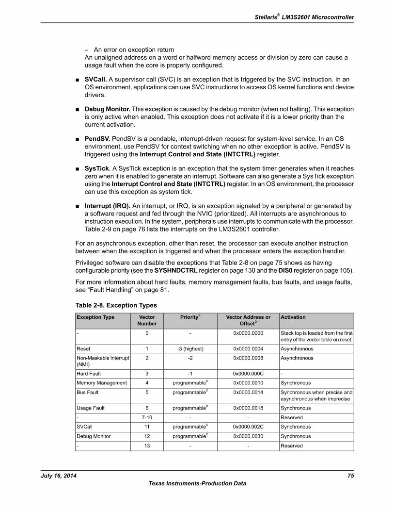
– An error on exception returnAn unaligned address on a word or halfword memory access or division by zero can cause ausage fault when the core is properly configured.
SVCall. A supervisor call (SVC) is an exception that is triggered by the SVC instruction. In anOS environment, applications can use SVC instructions to access OS kernel functions and devicedrivers.
DebugMonitor. This exception is caused by the debugmonitor (when not halting). This exceptionis only active when enabled. This exception does not activate if it is a lower priority than thecurrent activation.
PendSV. PendSV is a pendable, interrupt-driven request for system-level service. In an OSenvironment, use PendSV for context switching when no other exception is active. PendSV istriggered using the Interrupt Control and State (INTCTRL) register.
SysTick. A SysTick exception is an exception that the system timer generates when it reacheszero when it is enabled to generate an interrupt. Software can also generate a SysTick exceptionusing the Interrupt Control and State (INTCTRL) register. In an OS environment, the processorcan use this exception as system tick.
Interrupt (IRQ). An interrupt, or IRQ, is an exception signaled by a peripheral or generated bya software request and fed through the NVIC (prioritized). All interrupts are asynchronous toinstruction execution. In the system, peripherals use interrupts to communicate with the processor.Table 2-9 on page 76 lists the interrupts on the LM3S2601 controller.
For an asynchronous exception, other than reset, the processor can execute another instructionbetween when the exception is triggered and when the processor enters the exception handler.
Privileged software can disable the exceptions that Table 2-8 on page 75 shows as havingconfigurable priority (see theSYSHNDCTRL register on page 130 and theDIS0 register on page 105).
For more information about hard faults, memory management faults, bus faults, and usage faults,see “Fault Handling” on page 81.
Table 2-8. Exception Types
ActivationVector Address orOffsetb
PriorityaVectorNumber
Exception Type
Stack top is loaded from the firstentry of the vector table on reset.
0x0000.0000-0-
Asynchronous0x0000.0004-3 (highest)1Reset
Asynchronous0x0000.0008-22Non-Maskable Interrupt(NMI)
-0x0000.000C-13Hard Fault
Synchronous0x0000.0010programmablec4Memory Management
Synchronous when precise andasynchronous when imprecise
0x0000.0014programmablec5Bus Fault
Synchronous0x0000.0018programmablec6Usage Fault
Reserved--7-10-
Synchronous0x0000.002Cprogrammablec11SVCall
Synchronous0x0000.0030programmablec12Debug Monitor
Reserved--13-
75July 16, 2014Texas Instruments-Production Data
Stellaris® LM3S2601 Microcontroller
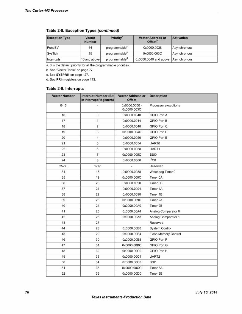
Table 2-8. Exception Types (continued)
ActivationVector Address orOffsetb
PriorityaVectorNumber
Exception Type
Asynchronous0x0000.0038programmablec14PendSV
Asynchronous0x0000.003Cprogrammablec15SysTick
Asynchronous0x0000.0040 and aboveprogrammabled16 and aboveInterrupts
a. 0 is the default priority for all the programmable priorities.b. See “Vector Table” on page 77.c. See SYSPRI1 on page 127.d. See PRIn registers on page 113.
Table 2-9. Interrupts
DescriptionVector Address orOffset
Interrupt Number (Bitin Interrupt Registers)
Vector Number
Processor exceptions0x0000.0000 -0x0000.003C
-0-15
GPIO Port A0x0000.0040016
GPIO Port B0x0000.0044117
GPIO Port C0x0000.0048218
GPIO Port D0x0000.004C319
GPIO Port E0x0000.0050420
UART00x0000.0054521
UART10x0000.0058622
SSI00x0000.005C723
I2C00x0000.0060824
Reserved-9-1725-33
Watchdog Timer 00x0000.00881834
Timer 0A0x0000.008C1935
Timer 0B0x0000.00902036
Timer 1A0x0000.00942137
Timer 1B0x0000.00982238
Timer 2A0x0000.009C2339
Timer 2B0x0000.00A02440
Analog Comparator 00x0000.00A42541
Analog Comparator 10x0000.00A82642
Reserved-2743
System Control0x0000.00B02844
Flash Memory Control0x0000.00B42945
GPIO Port F0x0000.00B83046
GPIO Port G0x0000.00BC3147
GPIO Port H0x0000.00C03248
UART20x0000.00C43349
SSI10x0000.00C83450
Timer 3A0x0000.00CC3551
Timer 3B0x0000.00D03652
July 16, 201476Texas Instruments-Production Data
The Cortex-M3 Processor
Table 2-9. Interrupts (continued)
DescriptionVector Address orOffset
Interrupt Number (Bitin Interrupt Registers)
Vector Number
I2C10x0000.00D43753
Reserved-3854
CAN00x0000.00DC3955
Reserved-40-4256-58
Hibernation Module0x0000.00EC4359
2.5.3 Exception HandlersThe processor handles exceptions using:
Interrupt Service Routines (ISRs). Interrupts (IRQx) are the exceptions handled by ISRs.
Fault Handlers. Hard fault, memory management fault, usage fault, and bus fault are faultexceptions handled by the fault handlers.
System Handlers. NMI, PendSV, SVCall, SysTick, and the fault exceptions are all systemexceptions that are handled by system handlers.
2.5.4 Vector TableThe vector table contains the reset value of the stack pointer and the start addresses, also calledexception vectors, for all exception handlers. The vector table is constructed using the vector addressor offset shown in Table 2-8 on page 75. Figure 2-6 on page 78 shows the order of the exceptionvectors in the vector table. The least-significant bit of each vector must be 1, indicating that theexception handler is Thumb code
77July 16, 2014Texas Instruments-Production Data
Stellaris® LM3S2601 Microcontroller
Figure 2-6. Vector Table
Initial SP value
Reset
Hard fault
NMI
Memory management fault
Usage fault
Bus fault
0x0000
0x0004
0x0008
0x000C
0x0010
0x0014
0x0018
Reserved
SVCall
PendSV
Reserved for Debug
Systick
IRQ0
Reserved
0x002C
0x0038
0x003C
0x0040
OffsetException number
2
3
4
5
6
11
12
14
15
16
18
13
7
10
1
Vector
.
.
.
8
9
IRQ1
IRQ2
0x0044
IRQ43
170x0048
0x004C
59
.
.
.
.
.
.
0x00EC
IRQ number
-14
-13
-12
-11
-10
-5
-2
-1
0
2
1
43
On system reset, the vector table is fixed at address 0x0000.0000. Privileged software can write tothe Vector Table Offset (VTABLE) register to relocate the vector table start address to a differentmemory location, in the range 0x0000.0100 to 0x3FFF.FF00 (see “Vector Table” on page 77). Notethat when configuring the VTABLE register, the offset must be aligned on a 256-byte boundary.
2.5.5 Exception PrioritiesAs Table 2-8 on page 75 shows, all exceptions have an associated priority, with a lower priorityvalue indicating a higher priority and configurable priorities for all exceptions except Reset, Hardfault, and NMI. If software does not configure any priorities, then all exceptions with a configurablepriority have a priority of 0. For information about configuring exception priorities, see page 127 andpage 113.
Note: Configurable priority values for the Stellaris implementation are in the range 0-7. This meansthat the Reset, Hard fault, and NMI exceptions, with fixed negative priority values, alwayshave higher priority than any other exception.
For example, assigning a higher priority value to IRQ[0] and a lower priority value to IRQ[1] meansthat IRQ[1] has higher priority than IRQ[0]. If both IRQ[1] and IRQ[0] are asserted, IRQ[1] is processedbefore IRQ[0].
July 16, 201478Texas Instruments-Production Data
The Cortex-M3 Processor
If multiple pending exceptions have the same priority, the pending exception with the lowest exceptionnumber takes precedence. For example, if both IRQ[0] and IRQ[1] are pending and have the samepriority, then IRQ[0] is processed before IRQ[1].
When the processor is executing an exception handler, the exception handler is preempted if ahigher priority exception occurs. If an exception occurs with the same priority as the exception beinghandled, the handler is not preempted, irrespective of the exception number. However, the statusof the new interrupt changes to pending.
2.5.6 Interrupt Priority GroupingTo increase priority control in systems with interrupts, the NVIC supports priority grouping. Thisgrouping divides each interrupt priority register entry into two fields:
An upper field that defines the group priority
A lower field that defines a subpriority within the group
Only the group priority determines preemption of interrupt exceptions. When the processor isexecuting an interrupt exception handler, another interrupt with the same group priority as theinterrupt being handled does not preempt the handler.
If multiple pending interrupts have the same group priority, the subpriority field determines the orderin which they are processed. If multiple pending interrupts have the same group priority andsubpriority, the interrupt with the lowest IRQ number is processed first.
For information about splitting the interrupt priority fields into group priority and subpriority, seepage 121.
2.5.7 Exception Entry and ReturnDescriptions of exception handling use the following terms:
Preemption.When the processor is executing an exception handler, an exception can preemptthe exception handler if its priority is higher than the priority of the exception being handled. See“Interrupt Priority Grouping” on page 79 for more information about preemption by an interrupt.When one exception preempts another, the exceptions are called nested exceptions. See“Exception Entry” on page 80 more information.
Return. Return occurs when the exception handler is completed, and there is no pendingexception with sufficient priority to be serviced and the completed exception handler was nothandling a late-arriving exception. The processor pops the stack and restores the processorstate to the state it had before the interrupt occurred. See “Exception Return” on page 81 formore information.
Tail-Chaining. This mechanism speeds up exception servicing. On completion of an exceptionhandler, if there is a pending exception that meets the requirements for exception entry, thestack pop is skipped and control transfers to the new exception handler.
Late-Arriving. This mechanism speeds up preemption. If a higher priority exception occursduring state saving for a previous exception, the processor switches to handle the higher priorityexception and initiates the vector fetch for that exception. State saving is not affected by latearrival because the state saved is the same for both exceptions. Therefore, the state savingcontinues uninterrupted. The processor can accept a late arriving exception until the first instructionof the exception handler of the original exception enters the execute stage of the processor. On
79July 16, 2014Texas Instruments-Production Data
Stellaris® LM3S2601 Microcontroller
return from the exception handler of the late-arriving exception, the normal tail-chaining rulesapply.
2.5.7.1 Exception EntryException entry occurs when there is a pending exception with sufficient priority and either theprocessor is in Thread mode or the new exception is of higher priority than the exception beinghandled, in which case the new exception preempts the original exception.
When one exception preempts another, the exceptions are nested.
Sufficient priority means the exception has more priority than any limits set by the mask registers(see PRIMASK on page 61, FAULTMASK on page 62, and BASEPRI on page 63). An exceptionwith less priority than this is pending but is not handled by the processor.
When the processor takes an exception, unless the exception is a tail-chained or a late-arrivingexception, the processor pushes information onto the current stack. This operation is referred to asstacking and the structure of eight data words is referred to as stack frame.
Figure 2-7. Exception Stack Frame
Pre-IRQ top of stack
xPSRPCLRR12R3R2R1R0
aligner
IRQ top of stack
...
Immediately after stacking, the stack pointer indicates the lowest address in the stack frame. Unlessstack alignment is disabled, the stack frame is aligned to a double-word address. If the STKALIGNbit of the Configuration Control (CCR) register is set, stack align adjustment is performed duringstacking.
The stack frame includes the return address, which is the address of the next instruction in theinterrupted program. This value is restored to the PC at exception return so that the interruptedprogram resumes.
In parallel to the stacking operation, the processor performs a vector fetch that reads the exceptionhandler start address from the vector table. When stacking is complete, the processor starts executingthe exception handler. At the same time, the processor writes an EXC_RETURN value to the LR,indicating which stack pointer corresponds to the stack frame and what operation mode the processorwas in before the entry occurred.
If no higher-priority exception occurs during exception entry, the processor starts executing theexception handler and automatically changes the status of the corresponding pending interrupt toactive.
If another higher-priority exception occurs during exception entry, known as late arrival, the processorstarts executing the exception handler for this exception and does not change the pending statusof the earlier exception.
July 16, 201480Texas Instruments-Production Data
The Cortex-M3 Processor
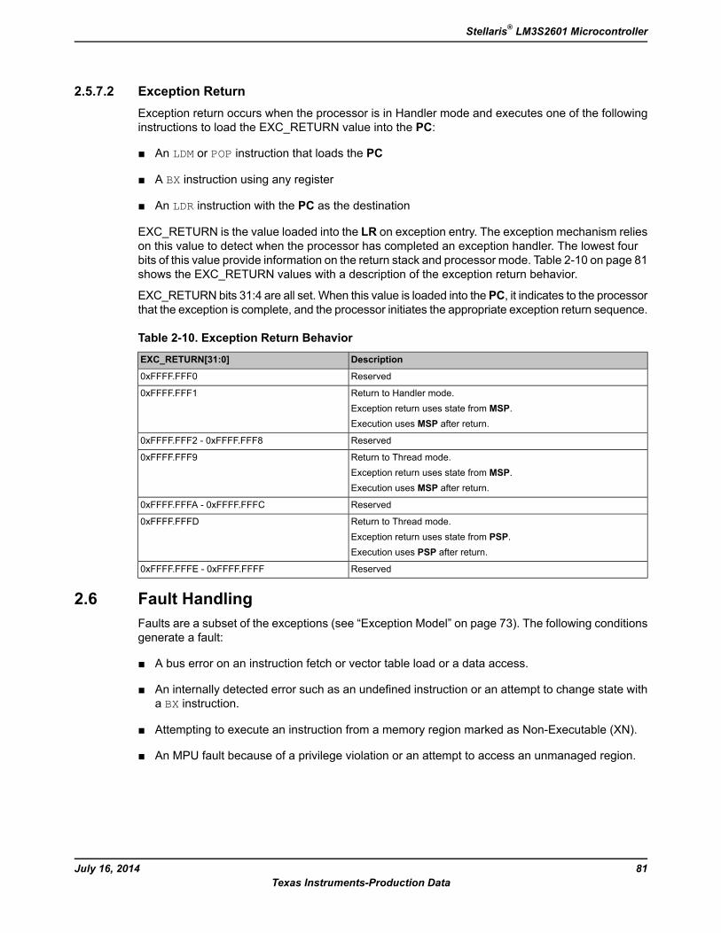
2.5.7.2 Exception ReturnException return occurs when the processor is in Handler mode and executes one of the followinginstructions to load the EXC_RETURN value into the PC:
An LDM or POP instruction that loads the PC
A BX instruction using any register
An LDR instruction with the PC as the destination
EXC_RETURN is the value loaded into the LR on exception entry. The exception mechanism relieson this value to detect when the processor has completed an exception handler. The lowest fourbits of this value provide information on the return stack and processor mode. Table 2-10 on page 81shows the EXC_RETURN values with a description of the exception return behavior.
EXC_RETURN bits 31:4 are all set. When this value is loaded into thePC, it indicates to the processorthat the exception is complete, and the processor initiates the appropriate exception return sequence.
Table 2-10. Exception Return Behavior
DescriptionEXC_RETURN[31:0]
Reserved0xFFFF.FFF0
Return to Handler mode.Exception return uses state from MSP.Execution uses MSP after return.
0xFFFF.FFF1
Reserved0xFFFF.FFF2 - 0xFFFF.FFF8
Return to Thread mode.Exception return uses state from MSP.Execution uses MSP after return.
0xFFFF.FFF9
Reserved0xFFFF.FFFA - 0xFFFF.FFFC
Return to Thread mode.Exception return uses state from PSP.Execution uses PSP after return.
0xFFFF.FFFD
Reserved0xFFFF.FFFE - 0xFFFF.FFFF
2.6 Fault HandlingFaults are a subset of the exceptions (see “Exception Model” on page 73). The following conditionsgenerate a fault:
A bus error on an instruction fetch or vector table load or a data access.
An internally detected error such as an undefined instruction or an attempt to change state witha BX instruction.
Attempting to execute an instruction from a memory region marked as Non-Executable (XN).
An MPU fault because of a privilege violation or an attempt to access an unmanaged region.
81July 16, 2014Texas Instruments-Production Data
Stellaris® LM3S2601 Microcontroller
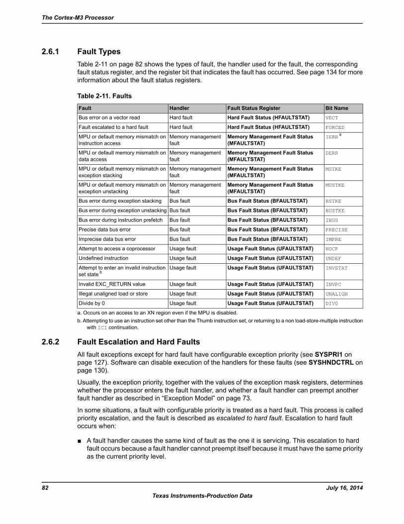
2.6.1 Fault TypesTable 2-11 on page 82 shows the types of fault, the handler used for the fault, the correspondingfault status register, and the register bit that indicates the fault has occurred. See page 134 for moreinformation about the fault status registers.
Table 2-11. Faults
Bit NameFault Status RegisterHandlerFault
VECTHard Fault Status (HFAULTSTAT)Hard faultBus error on a vector read
FORCEDHard Fault Status (HFAULTSTAT)Hard faultFault escalated to a hard fault
IERR aMemory Management Fault Status(MFAULTSTAT)
Memory managementfault
MPU or default memory mismatch oninstruction access
DERRMemory Management Fault Status(MFAULTSTAT)
Memory managementfault
MPU or default memory mismatch ondata access
MSTKEMemory Management Fault Status(MFAULTSTAT)
Memory managementfault
MPU or default memory mismatch onexception stacking
MUSTKEMemory Management Fault Status(MFAULTSTAT)
Memory managementfault
MPU or default memory mismatch onexception unstacking
BSTKEBus Fault Status (BFAULTSTAT)Bus faultBus error during exception stacking
BUSTKEBus Fault Status (BFAULTSTAT)Bus faultBus error during exception unstacking
IBUSBus Fault Status (BFAULTSTAT)Bus faultBus error during instruction prefetch
PRECISEBus Fault Status (BFAULTSTAT)Bus faultPrecise data bus error
IMPREBus Fault Status (BFAULTSTAT)Bus faultImprecise data bus error
NOCPUsage Fault Status (UFAULTSTAT)Usage faultAttempt to access a coprocessor
UNDEFUsage Fault Status (UFAULTSTAT)Usage faultUndefined instruction
INVSTATUsage Fault Status (UFAULTSTAT)Usage faultAttempt to enter an invalid instructionset state b
INVPCUsage Fault Status (UFAULTSTAT)Usage faultInvalid EXC_RETURN value
UNALIGNUsage Fault Status (UFAULTSTAT)Usage faultIllegal unaligned load or store
DIV0Usage Fault Status (UFAULTSTAT)Usage faultDivide by 0
a. Occurs on an access to an XN region even if the MPU is disabled.b. Attempting to use an instruction set other than the Thumb instruction set, or returning to a non load-store-multiple instruction
with ICI continuation.
2.6.2 Fault Escalation and Hard FaultsAll fault exceptions except for hard fault have configurable exception priority (see SYSPRI1 onpage 127). Software can disable execution of the handlers for these faults (see SYSHNDCTRL onpage 130).
Usually, the exception priority, together with the values of the exception mask registers, determineswhether the processor enters the fault handler, and whether a fault handler can preempt anotherfault handler as described in “Exception Model” on page 73.
In some situations, a fault with configurable priority is treated as a hard fault. This process is calledpriority escalation, and the fault is described as escalated to hard fault. Escalation to hard faultoccurs when:
A fault handler causes the same kind of fault as the one it is servicing. This escalation to hardfault occurs because a fault handler cannot preempt itself because it must have the same priorityas the current priority level.
July 16, 201482Texas Instruments-Production Data
The Cortex-M3 Processor
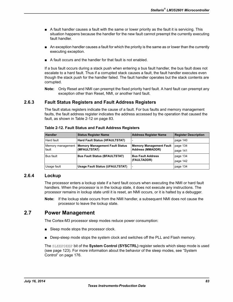
A fault handler causes a fault with the same or lower priority as the fault it is servicing. Thissituation happens because the handler for the new fault cannot preempt the currently executingfault handler.
An exception handler causes a fault for which the priority is the same as or lower than the currentlyexecuting exception.
A fault occurs and the handler for that fault is not enabled.
If a bus fault occurs during a stack push when entering a bus fault handler, the bus fault does notescalate to a hard fault. Thus if a corrupted stack causes a fault, the fault handler executes eventhough the stack push for the handler failed. The fault handler operates but the stack contents arecorrupted.
Note: Only Reset and NMI can preempt the fixed priority hard fault. A hard fault can preempt anyexception other than Reset, NMI, or another hard fault.
2.6.3 Fault Status Registers and Fault Address RegistersThe fault status registers indicate the cause of a fault. For bus faults and memory managementfaults, the fault address register indicates the address accessed by the operation that caused thefault, as shown in Table 2-12 on page 83.
Table 2-12. Fault Status and Fault Address Registers
Register DescriptionAddress Register NameStatus Register NameHandler
page 140-Hard Fault Status (HFAULTSTAT)Hard fault
page 134page 141
Memory Management FaultAddress (MMADDR)
Memory Management Fault Status(MFAULTSTAT)
Memory managementfault
page 134page 142
Bus Fault Address(FAULTADDR)
Bus Fault Status (BFAULTSTAT)Bus fault
page 134-Usage Fault Status (UFAULTSTAT)Usage fault
2.6.4 LockupThe processor enters a lockup state if a hard fault occurs when executing the NMI or hard faulthandlers. When the processor is in the lockup state, it does not execute any instructions. Theprocessor remains in lockup state until it is reset, an NMI occurs, or it is halted by a debugger.
Note: If the lockup state occurs from the NMI handler, a subsequent NMI does not cause theprocessor to leave the lockup state.
2.7 Power ManagementThe Cortex-M3 processor sleep modes reduce power consumption:
Sleep mode stops the processor clock.
Deep-sleep mode stops the system clock and switches off the PLL and Flash memory.
The SLEEPDEEP bit of the System Control (SYSCTRL) register selects which sleep mode is used(see page 123). For more information about the behavior of the sleep modes, see “SystemControl” on page 176.
83July 16, 2014Texas Instruments-Production Data
Stellaris® LM3S2601 Microcontroller
This section describes the mechanisms for entering sleep mode and the conditions for waking upfrom sleep mode, both of which apply to Sleep mode and Deep-sleep mode.
2.7.1 Entering Sleep ModesThis section describes the mechanisms software can use to put the processor into one of the sleepmodes.
The system can generate spurious wake-up events, for example a debug operation wakes up theprocessor. Therefore, software must be able to put the processor back into sleep mode after suchan event. A program might have an idle loop to put the processor back to sleep mode.
2.7.1.1 Wait for InterruptThe wait for interrupt instruction, WFI, causes immediate entry to sleep mode unless the wake-upcondition is true (see “Wake Up from WFI or Sleep-on-Exit” on page 84). When the processorexecutes a WFI instruction, it stops executing instructions and enters sleep mode. See theCortex™-M3/M4 Instruction Set Technical User's Manual for more information.
2.7.1.2 Wait for EventThe wait for event instruction, WFE, causes entry to sleep mode conditional on the value of a one-bitevent register. When the processor executes a WFE instruction, it checks the event register. If theregister is 0, the processor stops executing instructions and enters sleep mode. If the register is 1,the processor clears the register and continues executing instructions without entering sleep mode.
If the event register is 1, the processor must not enter sleep mode on execution of a WFE instruction.Typically, this situation occurs if an SEV instruction has been executed. Software cannot accessthis register directly.
See the Cortex™-M3/M4 Instruction Set Technical User's Manual for more information.
2.7.1.3 Sleep-on-ExitIf the SLEEPEXIT bit of the SYSCTRL register is set, when the processor completes the executionof all exception handlers, it returns to Thread mode and immediately enters sleep mode. Thismechanism can be used in applications that only require the processor to run when an exceptionoccurs.
2.7.2 Wake Up from Sleep ModeThe conditions for the processor to wake up depend on the mechanism that cause it to enter sleepmode.
2.7.2.1 Wake Up from WFI or Sleep-on-ExitNormally, the processor wakes up only when the NVIC detects an exception with sufficient priorityto cause exception entry. Some embedded systems might have to execute system restore tasksafter the processor wakes up and before executing an interrupt handler. Entry to the interrupt handlercan be delayed by setting the PRIMASK bit and clearing the FAULTMASK bit. If an interrupt arrivesthat is enabled and has a higher priority than current exception priority, the processor wakes up butdoes not execute the interrupt handler until the processor clears PRIMASK. For more informationabout PRIMASK and FAULTMASK, see page 61 and page 62.
2.7.2.2 Wake Up from WFEThe processor wakes up if it detects an exception with sufficient priority to cause exception entry.
July 16, 201484Texas Instruments-Production Data
The Cortex-M3 Processor
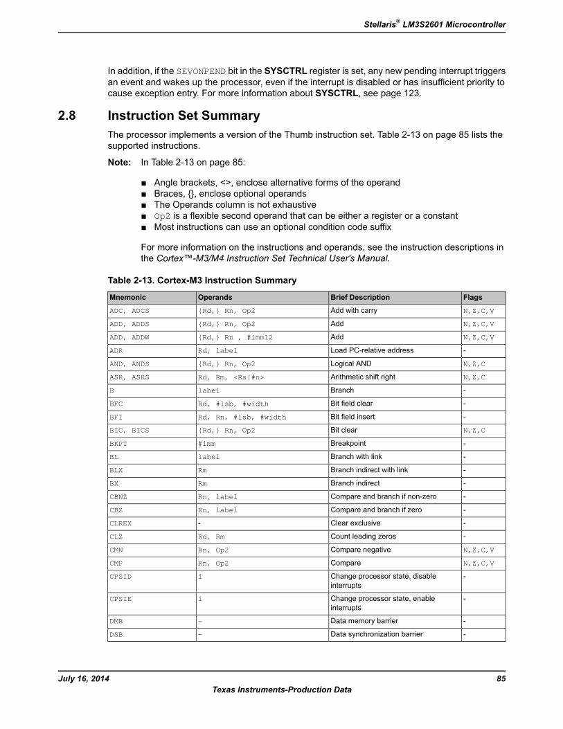
In addition, if the SEVONPEND bit in the SYSCTRL register is set, any new pending interrupt triggersan event and wakes up the processor, even if the interrupt is disabled or has insufficient priority tocause exception entry. For more information about SYSCTRL, see page 123.
2.8 Instruction Set SummaryThe processor implements a version of the Thumb instruction set. Table 2-13 on page 85 lists thesupported instructions.
Note: In Table 2-13 on page 85:
Angle brackets, <>, enclose alternative forms of the operand Braces, , enclose optional operands The Operands column is not exhaustive Op2 is a flexible second operand that can be either a register or a constant Most instructions can use an optional condition code suffix
For more information on the instructions and operands, see the instruction descriptions inthe Cortex™-M3/M4 Instruction Set Technical User's Manual.
Table 2-13. Cortex-M3 Instruction Summary
FlagsBrief DescriptionOperandsMnemonic
N,Z,C,VAdd with carryRd, Rn, Op2ADC, ADCS
N,Z,C,VAddRd, Rn, Op2ADD, ADDS
N,Z,C,VAddRd, Rn , #imm12ADD, ADDW
-Load PC-relative addressRd, labelADR
N,Z,CLogical ANDRd, Rn, Op2AND, ANDS
N,Z,CArithmetic shift rightRd, Rm, <Rs|#n>ASR, ASRS
-BranchlabelB
-Bit field clearRd, #lsb, #widthBFC
-Bit field insertRd, Rn, #lsb, #widthBFI
N,Z,CBit clearRd, Rn, Op2BIC, BICS
-Breakpoint#immBKPT
-Branch with linklabelBL
-Branch indirect with linkRmBLX
-Branch indirectRmBX
-Compare and branch if non-zeroRn, labelCBNZ
-Compare and branch if zeroRn, labelCBZ
-Clear exclusive-CLREX
-Count leading zerosRd, RmCLZ
N,Z,C,VCompare negativeRn, Op2CMN
N,Z,C,VCompareRn, Op2CMP
-Change processor state, disableinterrupts
iCPSID
-Change processor state, enableinterrupts
iCPSIE
-Data memory barrier-DMB
-Data synchronization barrier-DSB
85July 16, 2014Texas Instruments-Production Data
Stellaris® LM3S2601 Microcontroller
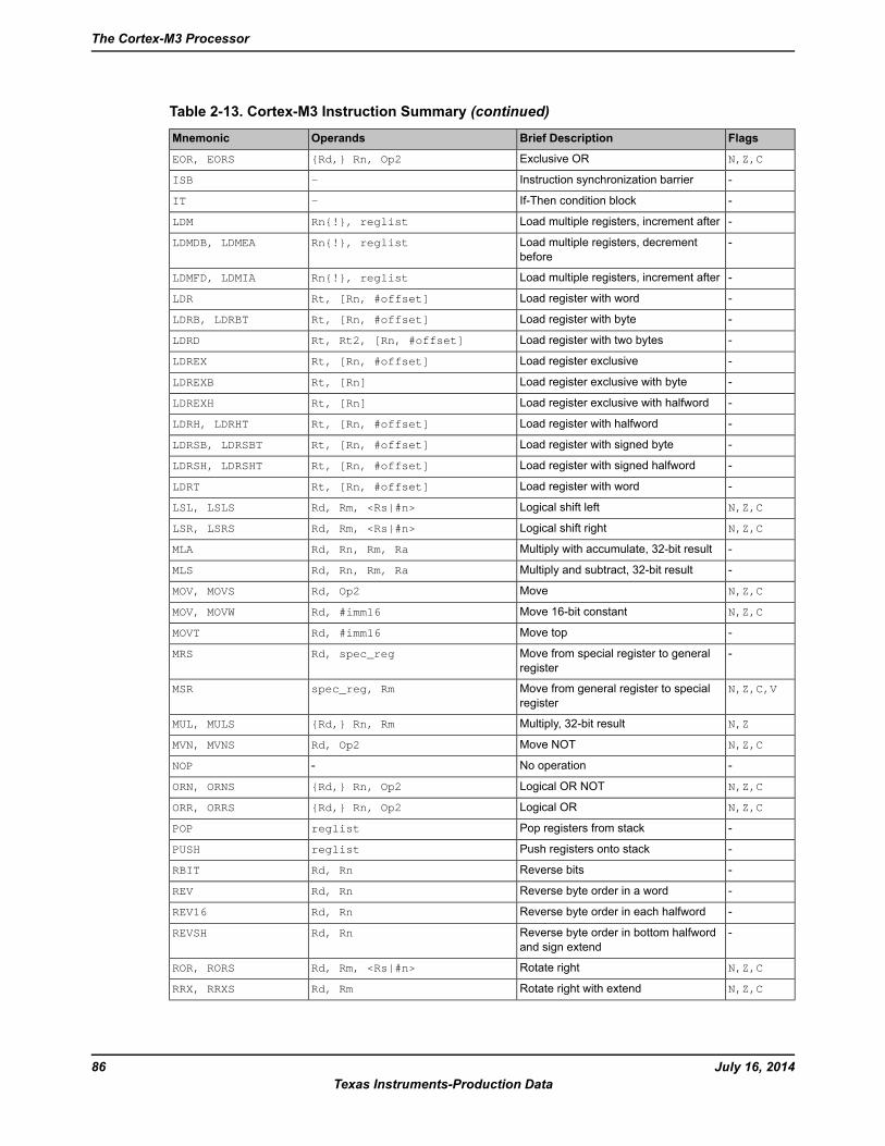
Table 2-13. Cortex-M3 Instruction Summary (continued)
FlagsBrief DescriptionOperandsMnemonic
N,Z,CExclusive ORRd, Rn, Op2EOR, EORS
-Instruction synchronization barrier-ISB
-If-Then condition block-IT
-Load multiple registers, increment afterRn!, reglistLDM
-Load multiple registers, decrementbefore
Rn!, reglistLDMDB, LDMEA
-Load multiple registers, increment afterRn!, reglistLDMFD, LDMIA
-Load register with wordRt, [Rn, #offset]LDR
-Load register with byteRt, [Rn, #offset]LDRB, LDRBT
-Load register with two bytesRt, Rt2, [Rn, #offset]LDRD
-Load register exclusiveRt, [Rn, #offset]LDREX
-Load register exclusive with byteRt, [Rn]LDREXB
-Load register exclusive with halfwordRt, [Rn]LDREXH
-Load register with halfwordRt, [Rn, #offset]LDRH, LDRHT
-Load register with signed byteRt, [Rn, #offset]LDRSB, LDRSBT
-Load register with signed halfwordRt, [Rn, #offset]LDRSH, LDRSHT
-Load register with wordRt, [Rn, #offset]LDRT
N,Z,CLogical shift leftRd, Rm, <Rs|#n>LSL, LSLS
N,Z,CLogical shift rightRd, Rm, <Rs|#n>LSR, LSRS
-Multiply with accumulate, 32-bit resultRd, Rn, Rm, RaMLA
-Multiply and subtract, 32-bit resultRd, Rn, Rm, RaMLS
N,Z,CMoveRd, Op2MOV, MOVS
N,Z,CMove 16-bit constantRd, #imm16MOV, MOVW
-Move topRd, #imm16MOVT
-Move from special register to generalregister
Rd, spec_regMRS
N,Z,C,VMove from general register to specialregister
spec_reg, RmMSR
N,ZMultiply, 32-bit resultRd, Rn, RmMUL, MULS
N,Z,CMove NOTRd, Op2MVN, MVNS
-No operation-NOP
N,Z,CLogical OR NOTRd, Rn, Op2ORN, ORNS
N,Z,CLogical ORRd, Rn, Op2ORR, ORRS
-Pop registers from stackreglistPOP
-Push registers onto stackreglistPUSH
-Reverse bitsRd, RnRBIT
-Reverse byte order in a wordRd, RnREV
-Reverse byte order in each halfwordRd, RnREV16
-Reverse byte order in bottom halfwordand sign extend
Rd, RnREVSH
N,Z,CRotate rightRd, Rm, <Rs|#n>ROR, RORS
N,Z,CRotate right with extendRd, RmRRX, RRXS
July 16, 201486Texas Instruments-Production Data
The Cortex-M3 Processor
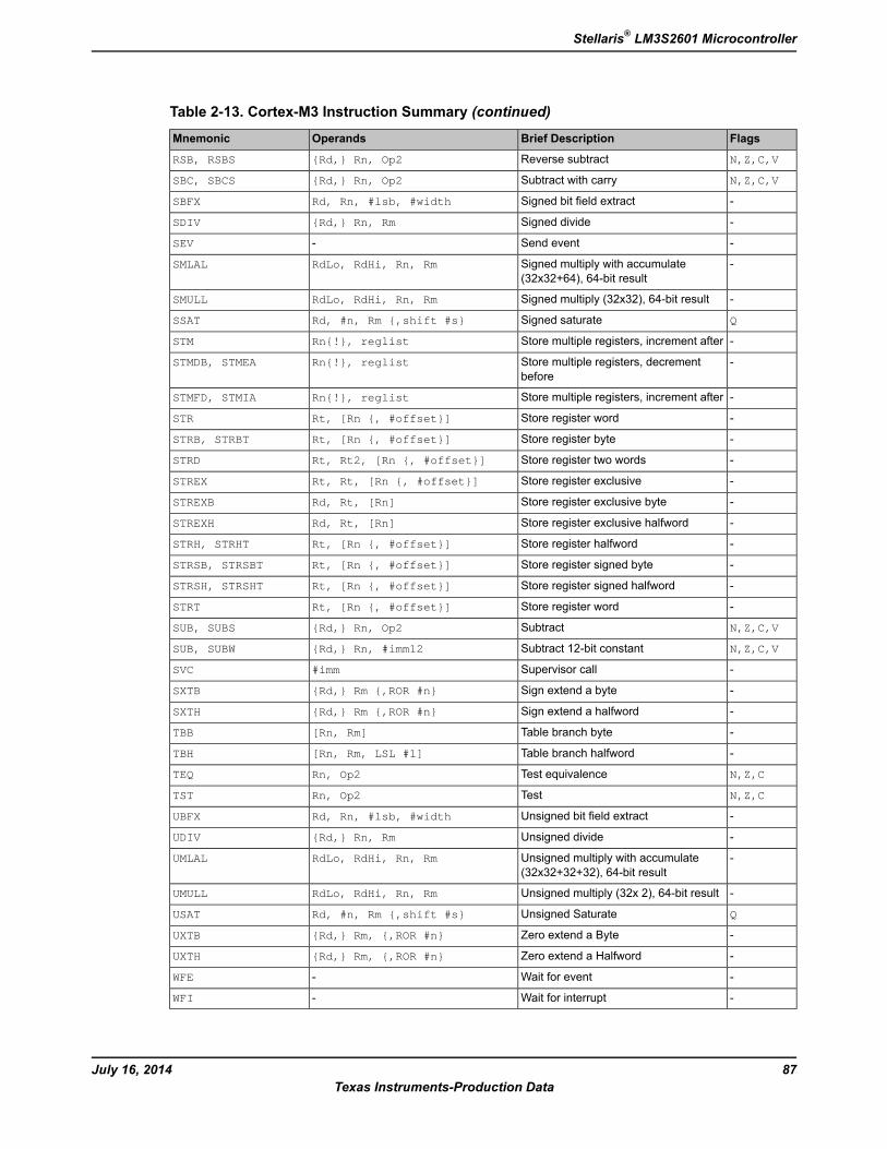
Table 2-13. Cortex-M3 Instruction Summary (continued)
FlagsBrief DescriptionOperandsMnemonic
N,Z,C,VReverse subtractRd, Rn, Op2RSB, RSBS
N,Z,C,VSubtract with carryRd, Rn, Op2SBC, SBCS
-Signed bit field extractRd, Rn, #lsb, #widthSBFX
-Signed divideRd, Rn, RmSDIV
-Send event-SEV
-Signed multiply with accumulate(32x32+64), 64-bit result
RdLo, RdHi, Rn, RmSMLAL
-Signed multiply (32x32), 64-bit resultRdLo, RdHi, Rn, RmSMULL
QSigned saturateRd, #n, Rm ,shift #sSSAT
-Store multiple registers, increment afterRn!, reglistSTM
-Store multiple registers, decrementbefore
Rn!, reglistSTMDB, STMEA
-Store multiple registers, increment afterRn!, reglistSTMFD, STMIA
-Store register wordRt, [Rn , #offset]STR
-Store register byteRt, [Rn , #offset]STRB, STRBT
-Store register two wordsRt, Rt2, [Rn , #offset]STRD
-Store register exclusiveRt, Rt, [Rn , #offset]STREX
-Store register exclusive byteRd, Rt, [Rn]STREXB
-Store register exclusive halfwordRd, Rt, [Rn]STREXH
-Store register halfwordRt, [Rn , #offset]STRH, STRHT
-Store register signed byteRt, [Rn , #offset]STRSB, STRSBT
-Store register signed halfwordRt, [Rn , #offset]STRSH, STRSHT
-Store register wordRt, [Rn , #offset]STRT
N,Z,C,VSubtractRd, Rn, Op2SUB, SUBS
N,Z,C,VSubtract 12-bit constantRd, Rn, #imm12SUB, SUBW
-Supervisor call#immSVC
-Sign extend a byteRd, Rm ,ROR #nSXTB
-Sign extend a halfwordRd, Rm ,ROR #nSXTH
-Table branch byte[Rn, Rm]TBB
-Table branch halfword[Rn, Rm, LSL #1]TBH
N,Z,CTest equivalenceRn, Op2TEQ
N,Z,CTestRn, Op2TST
-Unsigned bit field extractRd, Rn, #lsb, #widthUBFX
-Unsigned divideRd, Rn, RmUDIV
-Unsigned multiply with accumulate(32x32+32+32), 64-bit result
RdLo, RdHi, Rn, RmUMLAL
-Unsigned multiply (32x 2), 64-bit resultRdLo, RdHi, Rn, RmUMULL
QUnsigned SaturateRd, #n, Rm ,shift #sUSAT
-Zero extend a ByteRd, Rm, ,ROR #nUXTB
-Zero extend a HalfwordRd, Rm, ,ROR #nUXTH
-Wait for event-WFE
-Wait for interrupt-WFI
87July 16, 2014Texas Instruments-Production Data
Stellaris® LM3S2601 Microcontroller
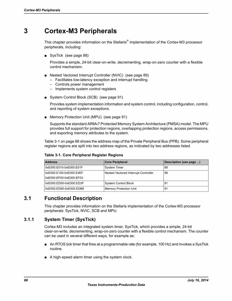
3 Cortex-M3 PeripheralsThis chapter provides information on the Stellaris® implementation of the Cortex-M3 processorperipherals, including:
SysTick (see page 88)
Provides a simple, 24-bit clear-on-write, decrementing, wrap-on-zero counter with a flexiblecontrol mechanism.
Nested Vectored Interrupt Controller (NVIC) (see page 89)– Facilitates low-latency exception and interrupt handling– Controls power management– Implements system control registers
System Control Block (SCB) (see page 91)
Provides system implementation information and system control, including configuration, control,and reporting of system exceptions.
Memory Protection Unit (MPU) (see page 91)
Supports the standard ARMv7 ProtectedMemory System Architecture (PMSA)model. TheMPUprovides full support for protection regions, overlapping protection regions, access permissions,and exporting memory attributes to the system.
Table 3-1 on page 88 shows the address map of the Private Peripheral Bus (PPB). Some peripheralregister regions are split into two address regions, as indicated by two addresses listed.
Table 3-1. Core Peripheral Register Regions
Description (see page ...)Core PeripheralAddress
88System Timer0xE000.E010-0xE000.E01F
89Nested Vectored Interrupt Controller0xE000.E100-0xE000.E4EF0xE000.EF00-0xE000.EF03
91System Control Block0xE000.ED00-0xE000.ED3F
91Memory Protection Unit0xE000.ED90-0xE000.EDB8
3.1 Functional DescriptionThis chapter provides information on the Stellaris implementation of the Cortex-M3 processorperipherals: SysTick, NVIC, SCB and MPU.
3.1.1 System Timer (SysTick)Cortex-M3 includes an integrated system timer, SysTick, which provides a simple, 24-bitclear-on-write, decrementing, wrap-on-zero counter with a flexible control mechanism. The countercan be used in several different ways, for example as:
An RTOS tick timer that fires at a programmable rate (for example, 100 Hz) and invokes a SysTickroutine.
A high-speed alarm timer using the system clock.
July 16, 201488Texas Instruments-Production Data
Cortex-M3 Peripherals
A variable rate alarm or signal timer—the duration is range-dependent on the reference clockused and the dynamic range of the counter.
A simple counter used to measure time to completion and time used.
An internal clock source control based on missing/meeting durations. The COUNT bit in theSTCTRL control and status register can be used to determine if an action completed within aset duration, as part of a dynamic clock management control loop.
The timer consists of three registers:
SysTick Control and Status (STCTRL): A control and status counter to configure its clock,enable the counter, enable the SysTick interrupt, and determine counter status.
SysTick Reload Value (STRELOAD): The reload value for the counter, used to provide thecounter's wrap value.
SysTick Current Value (STCURRENT): The current value of the counter.
When enabled, the timer counts down on each clock from the reload value to zero, reloads (wraps)to the value in the STRELOAD register on the next clock edge, then decrements on subsequentclocks. Clearing the STRELOAD register disables the counter on the next wrap. When the counterreaches zero, the COUNT status bit is set. The COUNT bit clears on reads.
Writing to the STCURRENT register clears the register and the COUNT status bit. The write doesnot trigger the SysTick exception logic. On a read, the current value is the value of the register atthe time the register is accessed.
The SysTick counter runs on the system clock. If this clock signal is stopped for low power mode,the SysTick counter stops. Ensure software uses aligned word accesses to access the SysTickregisters.
Note: When the processor is halted for debugging, the counter does not decrement.
3.1.2 Nested Vectored Interrupt Controller (NVIC)This section describes the Nested Vectored Interrupt Controller (NVIC) and the registers it uses.The NVIC supports:
30 interrupts.
A programmable priority level of 0-7 for each interrupt. A higher level corresponds to a lowerpriority, so level 0 is the highest interrupt priority.
Low-latency exception and interrupt handling.
Level and pulse detection of interrupt signals.
Dynamic reprioritization of interrupts.
Grouping of priority values into group priority and subpriority fields.
Interrupt tail-chaining.
An external Non-maskable interrupt (NMI).
89July 16, 2014Texas Instruments-Production Data
Stellaris® LM3S2601 Microcontroller
The processor automatically stacks its state on exception entry and unstacks this state on exceptionexit, with no instruction overhead, providing low latency exception handling.
3.1.2.1 Level-Sensitive and Pulse InterruptsThe processor supports both level-sensitive and pulse interrupts. Pulse interrupts are also describedas edge-triggered interrupts.
A level-sensitive interrupt is held asserted until the peripheral deasserts the interrupt signal. Typicallythis happens because the ISR accesses the peripheral, causing it to clear the interrupt request. Apulse interrupt is an interrupt signal sampled synchronously on the rising edge of the processorclock. To ensure the NVIC detects the interrupt, the peripheral must assert the interrupt signal forat least one clock cycle, during which the NVIC detects the pulse and latches the interrupt.
When the processor enters the ISR, it automatically removes the pending state from the interrupt(see “Hardware and Software Control of Interrupts” on page 90 for more information). For alevel-sensitive interrupt, if the signal is not deasserted before the processor returns from the ISR,the interrupt becomes pending again, and the processor must execute its ISR again. As a result,the peripheral can hold the interrupt signal asserted until it no longer needs servicing.
3.1.2.2 Hardware and Software Control of InterruptsThe Cortex-M3 latches all interrupts. A peripheral interrupt becomes pending for one of the followingreasons:
The NVIC detects that the interrupt signal is High and the interrupt is not active.
The NVIC detects a rising edge on the interrupt signal.
Software writes to the corresponding interrupt set-pending register bit, or to the Software TriggerInterrupt (SWTRIG) register to make a Software-Generated Interrupt pending. See the INT bitin the PEND0 register on page 107 or SWTRIG on page 115.
A pending interrupt remains pending until one of the following:
The processor enters the ISR for the interrupt, changing the state of the interrupt from pendingto active. Then:
– For a level-sensitive interrupt, when the processor returns from the ISR, the NVIC samplesthe interrupt signal. If the signal is asserted, the state of the interrupt changes to pending,which might cause the processor to immediately re-enter the ISR. Otherwise, the state of theinterrupt changes to inactive.
– For a pulse interrupt, the NVIC continues to monitor the interrupt signal, and if this is pulsedthe state of the interrupt changes to pending and active. In this case, when the processorreturns from the ISR the state of the interrupt changes to pending, which might cause theprocessor to immediately re-enter the ISR.
If the interrupt signal is not pulsed while the processor is in the ISR, when the processorreturns from the ISR the state of the interrupt changes to inactive.
Software writes to the corresponding interrupt clear-pending register bit
– For a level-sensitive interrupt, if the interrupt signal is still asserted, the state of the interruptdoes not change. Otherwise, the state of the interrupt changes to inactive.
July 16, 201490Texas Instruments-Production Data
Cortex-M3 Peripherals
– For a pulse interrupt, the state of the interrupt changes to inactive, if the state was pendingor to active, if the state was active and pending.
3.1.3 System Control Block (SCB)The System Control Block (SCB) provides system implementation information and system control,including configuration, control, and reporting of the system exceptions.
3.1.4 Memory Protection Unit (MPU)This section describes the Memory protection unit (MPU). The MPU divides the memory map intoa number of regions and defines the location, size, access permissions, and memory attributes ofeach region. The MPU supports independent attribute settings for each region, overlapping regions,and export of memory attributes to the system.
The memory attributes affect the behavior of memory accesses to the region. The Cortex-M3 MPUdefines eight separate memory regions, 0-7, and a background region.
When memory regions overlap, a memory access is affected by the attributes of the region with thehighest number. For example, the attributes for region 7 take precedence over the attributes of anyregion that overlaps region 7.
The background region has the same memory access attributes as the default memory map, but isaccessible from privileged software only.
The Cortex-M3 MPU memory map is unified, meaning that instruction accesses and data accesseshave the same region settings.
If a program accesses a memory location that is prohibited by the MPU, the processor generatesa memory management fault, causing a fault exception and possibly causing termination of theprocess in an OS environment. In an OS environment, the kernel can update the MPU region settingdynamically based on the process to be executed. Typically, an embedded OS uses the MPU formemory protection.
Configuration of MPU regions is based on memory types (see “Memory Regions, Types andAttributes” on page 67 for more information).
Table 3-2 on page 91 shows the possible MPU region attributes. See the section called “MPUConfiguration for a Stellaris Microcontroller” on page 95 for guidelines for programming amicrocontroller implementation.
Table 3-2. Memory Attributes Summary
DescriptionMemory Type
All accesses to Strongly Ordered memory occur in program order.Strongly Ordered
Memory-mapped peripheralsDevice
Normal memoryNormal
To avoid unexpected behavior, disable the interrupts before updating the attributes of a region thatthe interrupt handlers might access.
Ensure software uses aligned accesses of the correct size to access MPU registers:
Except for the MPU Region Attribute and Size (MPUATTR) register, all MPU registers mustbe accessed with aligned word accesses.
The MPUATTR register can be accessed with byte or aligned halfword or word accesses.
91July 16, 2014Texas Instruments-Production Data
Stellaris® LM3S2601 Microcontroller
The processor does not support unaligned accesses to MPU registers.
When setting up the MPU, and if the MPU has previously been programmed, disable unused regionsto prevent any previous region settings from affecting the new MPU setup.
3.1.4.1 Updating an MPU RegionTo update the attributes for an MPU region, the MPU Region Number (MPUNUMBER), MPURegion Base Address (MPUBASE) and MPUATTR registers must be updated. Each register canbe programmed separately or with a multiple-word write to program all of these registers. You canuse the MPUBASEx and MPUATTRx aliases to program up to four regions simultaneously usingan STM instruction.
Updating an MPU Region Using Separate Words
This example simple code configures one region:
; R1 = region number; R2 = size/enable; R3 = attributes; R4 = address LDR R0,=MPUNUMBER ; 0xE000ED98, MPU region number register STR R1, [R0, #0x0] ; Region NumberSTR R4, [R0, #0x4] ; Region Base AddressSTRH R2, [R0, #0x8] ; Region Size and EnableSTRH R3, [R0, #0xA] ; Region Attribute
Disable a region before writing new region settings to the MPU if you have previously enabled theregion being changed. For example:
; R1 = region number; R2 = size/enable; R3 = attributes; R4 = addressLDR R0,=MPUNUMBER ; 0xE000ED98, MPU region number registerSTR R1, [R0, #0x0] ; Region NumberBIC R2, R2, #1 ; DisableSTRH R2, [R0, #0x8] ; Region Size and EnableSTR R4, [R0, #0x4] ; Region Base AddressSTRH R3, [R0, #0xA] ; Region AttributeORR R2, #1 ; EnableSTRH R2, [R0, #0x8] ; Region Size and Enable
Software must use memory barrier instructions:
Before MPU setup, if there might be outstanding memory transfers, such as buffered writes, thatmight be affected by the change in MPU settings.
After MPU setup, if it includes memory transfers that must use the new MPU settings.
However, memory barrier instructions are not required if the MPU setup process starts by enteringan exception handler, or is followed by an exception return, because the exception entry andexception return mechanism cause memory barrier behavior.
Software does not need any memory barrier instructions during MPU setup, because it accessesthe MPU through the Private Peripheral Bus (PPB), which is a Strongly Ordered memory region.
July 16, 201492Texas Instruments-Production Data
Cortex-M3 Peripherals
For example, if all of the memory access behavior is intended to take effect immediately after theprogramming sequence, then a DSB instruction and an ISB instruction should be used. A DSB isrequired after changing MPU settings, such as at the end of context switch. An ISB is required ifthe code that programs the MPU region or regions is entered using a branch or call. If theprogramming sequence is entered using a return from exception, or by taking an exception, thenan ISB is not required.
Updating an MPU Region Using Multi-Word Writes
The MPU can be programmed directly using multi-word writes, depending how the information isdivided. Consider the following reprogramming:
; R1 = region number; R2 = address; R3 = size, attributes in oneLDR R0, =MPUNUMBER ; 0xE000ED98, MPU region number registerSTR R1, [R0, #0x0] ; Region NumberSTR R2, [R0, #0x4] ; Region Base AddressSTR R3, [R0, #0x8] ; Region Attribute, Size and Enable
An STM instruction can be used to optimize this:
; R1 = region number; R2 = address; R3 = size, attributes in oneLDR R0, =MPUNUMBER ; 0xE000ED98, MPU region number registerSTM R0, R1-R3 ; Region number, address, attribute, size and enable
This operation can be done in two words for pre-packed information, meaning that theMPU RegionBase Address (MPUBASE) register (see page 147) contains the required region number and hasthe VALID bit set. This method can be used when the data is statically packed, for example in aboot loader:
; R1 = address and region number in one; R2 = size and attributes in oneLDR R0, =MPUBASE ; 0xE000ED9C, MPU Region Base registerSTR R1, [R0, #0x0] ; Region base address and region number combined ; with VALID (bit 4) setSTR R2, [R0, #0x4] ; Region Attribute, Size and Enable
Subregions
Regions of 256 bytes or more are divided into eight equal-sized subregions. Set the correspondingbit in the SRD field of the MPU Region Attribute and Size (MPUATTR) register (see page 149) todisable a subregion. The least-significant bit of the SRD field controls the first subregion, and themost-significant bit controls the last subregion. Disabling a subregion means another regionoverlapping the disabled range matches instead. If no other enabled region overlaps the disabledsubregion, the MPU issues a fault.
Regions of 32, 64, and 128 bytes do not support subregions. With regions of these sizes, the SRDfield must be configured to 0x00, otherwise the MPU behavior is unpredictable.
93July 16, 2014Texas Instruments-Production Data
Stellaris® LM3S2601 Microcontroller
Example of SRD Use
Two regions with the same base address overlap. Region one is 128 KB, and region two is 512 KB.To ensure the attributes from region one apply to the first 128 KB region, configure the SRD field forregion two to 0x03 to disable the first two subregions, as Figure 3-1 on page 94 shows.
Figure 3-1. SRD Use Example
Region 1
Disabled subregionDisabled subregion
Region 2, withsubregions
Base address of both regions
Offset frombase address
064KB128KB192KB256KB320KB384KB448KB512KB
3.1.4.2 MPU Access Permission AttributesThe access permission bits, TEX, S, C, B, AP, and XN of the MPUATTR register, control access tothe corresponding memory region. If an access is made to an area of memory without the requiredpermissions, then the MPU generates a permission fault.
Table 3-3 on page 94 shows the encodings for the TEX, C, B, and S access permission bits. Allencodings are shown for completeness, however the current implementation of the Cortex-M3 doesnot support the concept of cacheability or shareability. Refer to the section called “MPUConfigurationfor a Stellaris Microcontroller” on page 95 for information on programming the MPU for Stellarisimplementations.
Table 3-3. TEX, S, C, and B Bit Field Encoding
Other AttributesShareabilityMemory TypeBCSTEX
-ShareableStrongly Ordered00xa000b
-ShareableDevice10xa000
Outer and innerwrite-through. No writeallocate.
Not shareableNormal010000
ShareableNormal011000
Not shareableNormal110000
ShareableNormal111000
Outer and innernoncacheable.
Not shareableNormal000001
ShareableNormal001001
--Reserved encoding10xa001
--Reserved encoding01xa001
Outer and innerwrite-back. Write andread allocate.
Not shareableNormal110001
ShareableNormal111001
Nonshared Device.Not shareableDevice00xa010
--Reserved encoding10xa010
--Reserved encodingxa1xa010
July 16, 201494Texas Instruments-Production Data
Cortex-M3 Peripherals
Table 3-3. TEX, S, C, and B Bit Field Encoding (continued)
Other AttributesShareabilityMemory TypeBCSTEX
Cached memory (BB =outer policy, AA = innerpolicy).See Table 3-4 for theencoding of the AA andBB bits.
Not shareableNormalAA01BB
ShareableNormalAA11BB
a. The MPU ignores the value of this bit.
Table 3-4 on page 95 shows the cache policy for memory attribute encodings with a TEX value inthe range of 0x4-0x7.
Table 3-4. Cache Policy for Memory Attribute Encoding
Corresponding Cache PolicyEncoding, AA or BB
Non-cacheable00
Write back, write and read allocate01
Write through, no write allocate10
Write back, no write allocate11
Table 3-5 on page 95 shows the AP encodings in the MPUATTR register that define the accesspermissions for privileged and unprivileged software.
Table 3-5. AP Bit Field Encoding
DescriptionUnprivilegedPermissions
PrivilegedPermissions
AP Bit Field
All accesses generate a permission fault.No accessNo access000
Access from privileged software only.No accessR/W001
Writes by unprivileged software generate apermission fault.
ROR/W010
Full access.R/WR/W011
Reserved.UnpredictableUnpredictable100
Reads by privileged software only.No accessRO101
Read-only, by privileged or unprivileged software.RORO110
Read-only, by privileged or unprivileged software.RORO111
MPU Configuration for a Stellaris Microcontroller
Stellaris microcontrollers have only a single processor and no caches. As a result, the MPU shouldbe programmed as shown in Table 3-6 on page 95.
Table 3-6. Memory Region Attributes for Stellaris Microcontrollers
Memory Type and AttributesBCSTEXMemory Region
Normal memory, non-shareable, write-through010000bFlash memory
Normal memory, shareable, write-through011000bInternal SRAM
Normal memory, shareable, write-back,write-allocate
111000bExternal SRAM
Device memory, shareable101000bPeripherals
95July 16, 2014Texas Instruments-Production Data
Stellaris® LM3S2601 Microcontroller
In current Stellaris microcontroller implementations, the shareability and cache policy attributes donot affect the system behavior. However, using these settings for the MPU regions can make theapplication code more portable. The values given are for typical situations.
3.1.4.3 MPU MismatchWhen an access violates the MPU permissions, the processor generates a memory managementfault (see “Exceptions and Interrupts” on page 65 for more information). TheMFAULTSTAT registerindicates the cause of the fault. See page 134 for more information.
3.2 Register MapTable 3-7 on page 96 lists the Cortex-M3 Peripheral SysTick, NVIC, MPU and SCB registers. Theoffset listed is a hexadecimal increment to the register's address, relative to the Core Peripheralsbase address of 0xE000.E000.
Note: Register spaces that are not used are reserved for future or internal use. Software shouldnot modify any reserved memory address.
Table 3-7. Peripherals Register Map
SeepageDescriptionResetTypeNameOffset
System Timer (SysTick) Registers
99SysTick Control and Status Register0x0000.0000R/WSTCTRL0x010
101SysTick Reload Value Register0x0000.0000R/WSTRELOAD0x014
102SysTick Current Value Register0x0000.0000R/WCSTCURRENT0x018
Nested Vectored Interrupt Controller (NVIC) Registers
103Interrupt 0-31 Set Enable0x0000.0000R/WEN00x100
104Interrupt 32-43 Set Enable0x0000.0000R/WEN10x104
105Interrupt 0-31 Clear Enable0x0000.0000R/WDIS00x180
106Interrupt 32-43 Clear Enable0x0000.0000R/WDIS10x184
107Interrupt 0-31 Set Pending0x0000.0000R/WPEND00x200
108Interrupt 32-43 Set Pending0x0000.0000R/WPEND10x204
109Interrupt 0-31 Clear Pending0x0000.0000R/WUNPEND00x280
110Interrupt 32-43 Clear Pending0x0000.0000R/WUNPEND10x284
111Interrupt 0-31 Active Bit0x0000.0000ROACTIVE00x300
112Interrupt 32-43 Active Bit0x0000.0000ROACTIVE10x304
113Interrupt 0-3 Priority0x0000.0000R/WPRI00x400
113Interrupt 4-7 Priority0x0000.0000R/WPRI10x404
113Interrupt 8-11 Priority0x0000.0000R/WPRI20x408
113Interrupt 12-15 Priority0x0000.0000R/WPRI30x40C
113Interrupt 16-19 Priority0x0000.0000R/WPRI40x410
July 16, 201496Texas Instruments-Production Data
Cortex-M3 Peripherals
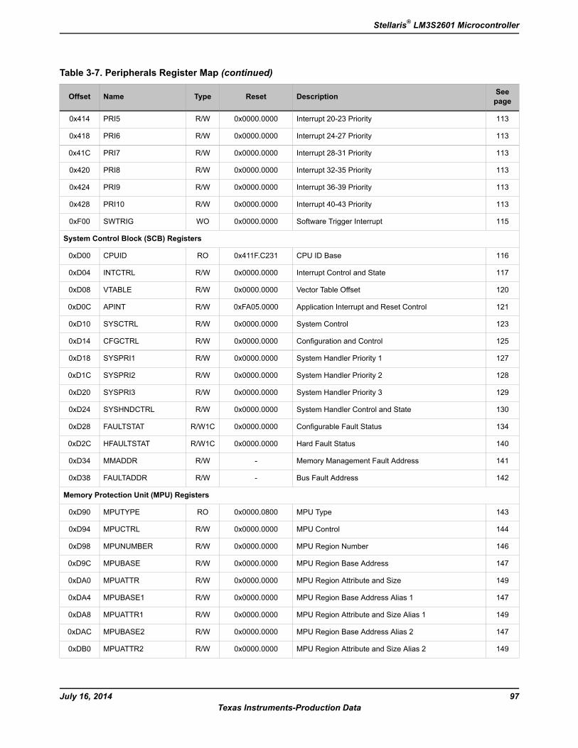
Table 3-7. Peripherals Register Map (continued)
SeepageDescriptionResetTypeNameOffset
113Interrupt 20-23 Priority0x0000.0000R/WPRI50x414
113Interrupt 24-27 Priority0x0000.0000R/WPRI60x418
113Interrupt 28-31 Priority0x0000.0000R/WPRI70x41C
113Interrupt 32-35 Priority0x0000.0000R/WPRI80x420
113Interrupt 36-39 Priority0x0000.0000R/WPRI90x424
113Interrupt 40-43 Priority0x0000.0000R/WPRI100x428
115Software Trigger Interrupt0x0000.0000WOSWTRIG0xF00
System Control Block (SCB) Registers
116CPU ID Base0x411F.C231ROCPUID0xD00
117Interrupt Control and State0x0000.0000R/WINTCTRL0xD04
120Vector Table Offset0x0000.0000R/WVTABLE0xD08
121Application Interrupt and Reset Control0xFA05.0000R/WAPINT0xD0C
123System Control0x0000.0000R/WSYSCTRL0xD10
125Configuration and Control0x0000.0000R/WCFGCTRL0xD14
127System Handler Priority 10x0000.0000R/WSYSPRI10xD18
128System Handler Priority 20x0000.0000R/WSYSPRI20xD1C
129System Handler Priority 30x0000.0000R/WSYSPRI30xD20
130System Handler Control and State0x0000.0000R/WSYSHNDCTRL0xD24
134Configurable Fault Status0x0000.0000R/W1CFAULTSTAT0xD28
140Hard Fault Status0x0000.0000R/W1CHFAULTSTAT0xD2C
141Memory Management Fault Address-R/WMMADDR0xD34
142Bus Fault Address-R/WFAULTADDR0xD38
Memory Protection Unit (MPU) Registers
143MPU Type0x0000.0800ROMPUTYPE0xD90
144MPU Control0x0000.0000R/WMPUCTRL0xD94
146MPU Region Number0x0000.0000R/WMPUNUMBER0xD98
147MPU Region Base Address0x0000.0000R/WMPUBASE0xD9C
149MPU Region Attribute and Size0x0000.0000R/WMPUATTR0xDA0
147MPU Region Base Address Alias 10x0000.0000R/WMPUBASE10xDA4
149MPU Region Attribute and Size Alias 10x0000.0000R/WMPUATTR10xDA8
147MPU Region Base Address Alias 20x0000.0000R/WMPUBASE20xDAC
149MPU Region Attribute and Size Alias 20x0000.0000R/WMPUATTR20xDB0
97July 16, 2014Texas Instruments-Production Data
Stellaris® LM3S2601 Microcontroller
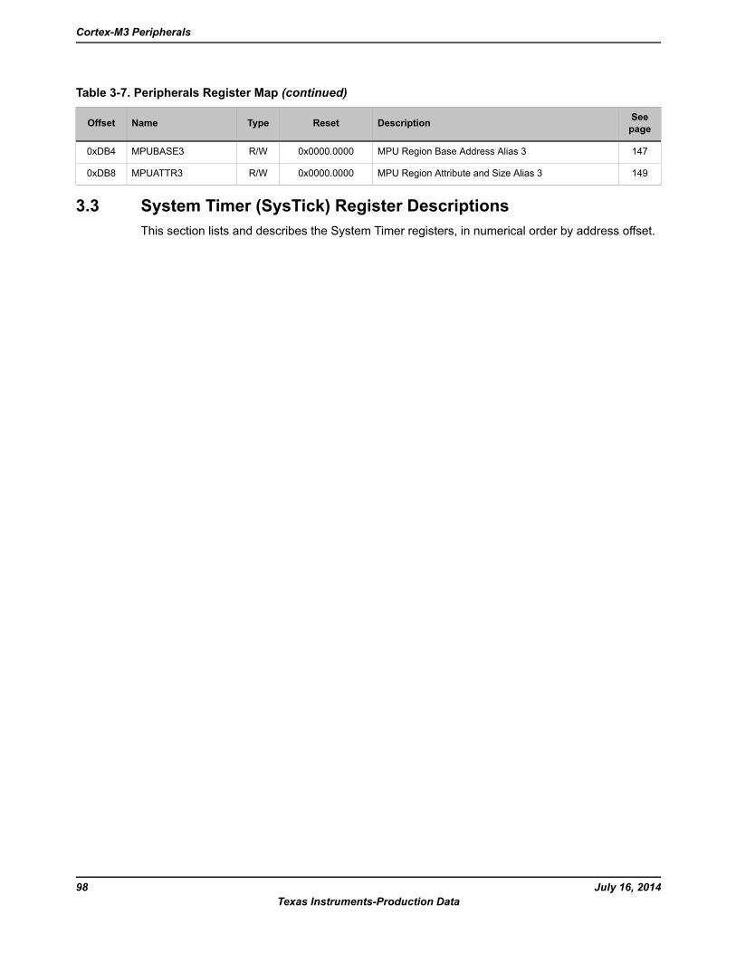
Table 3-7. Peripherals Register Map (continued)
SeepageDescriptionResetTypeNameOffset
147MPU Region Base Address Alias 30x0000.0000R/WMPUBASE30xDB4
149MPU Region Attribute and Size Alias 30x0000.0000R/WMPUATTR30xDB8
3.3 System Timer (SysTick) Register DescriptionsThis section lists and describes the System Timer registers, in numerical order by address offset.
July 16, 201498Texas Instruments-Production Data
Cortex-M3 Peripherals
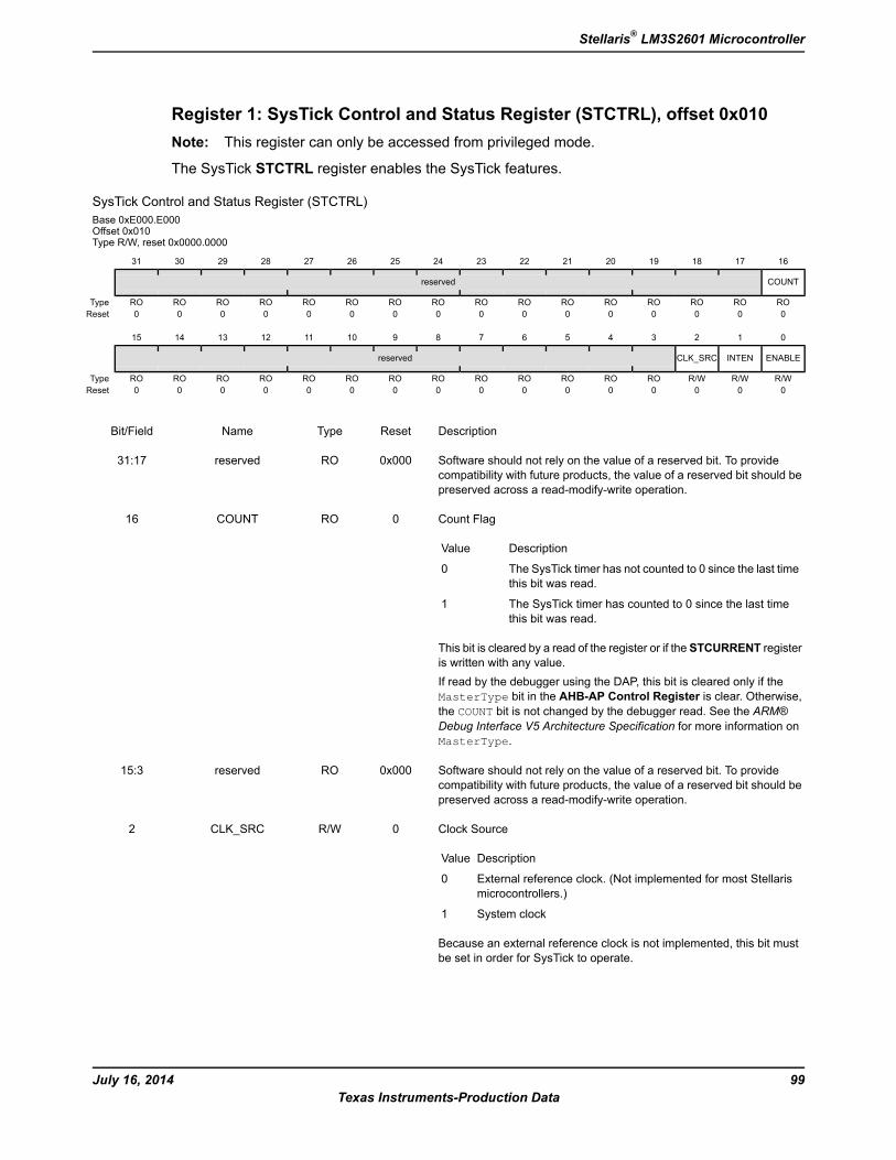
Register 1: SysTick Control and Status Register (STCTRL), offset 0x010Note: This register can only be accessed from privileged mode.
The SysTick STCTRL register enables the SysTick features.
SysTick Control and Status Register (STCTRL)Base 0xE000.E000Offset 0x010Type R/W, reset 0x0000.0000
16171819202122232425262728293031
COUNTreserved
ROROROROROROROROROROROROROROROROType0000000000000000Reset
0123456789101112131415
ENABLEINTENCLK_SRCreserved
R/WR/WR/WROROROROROROROROROROROROROType0000000000000000Reset
DescriptionResetTypeNameBit/Field
Software should not rely on the value of a reserved bit. To providecompatibility with future products, the value of a reserved bit should bepreserved across a read-modify-write operation.
0x000ROreserved31:17
Count Flag
DescriptionValue
The SysTick timer has not counted to 0 since the last timethis bit was read.
0
The SysTick timer has counted to 0 since the last timethis bit was read.
1
This bit is cleared by a read of the register or if the STCURRENT registeris written with any value.If read by the debugger using the DAP, this bit is cleared only if theMasterType bit in the AHB-AP Control Register is clear. Otherwise,the COUNT bit is not changed by the debugger read. See the ARM®Debug Interface V5 Architecture Specification for more information onMasterType.
0ROCOUNT16
Software should not rely on the value of a reserved bit. To providecompatibility with future products, the value of a reserved bit should bepreserved across a read-modify-write operation.
0x000ROreserved15:3
Clock Source
DescriptionValue
External reference clock. (Not implemented for most Stellarismicrocontrollers.)
0
System clock1
Because an external reference clock is not implemented, this bit mustbe set in order for SysTick to operate.
0R/WCLK_SRC2
99July 16, 2014Texas Instruments-Production Data
Stellaris® LM3S2601 Microcontroller
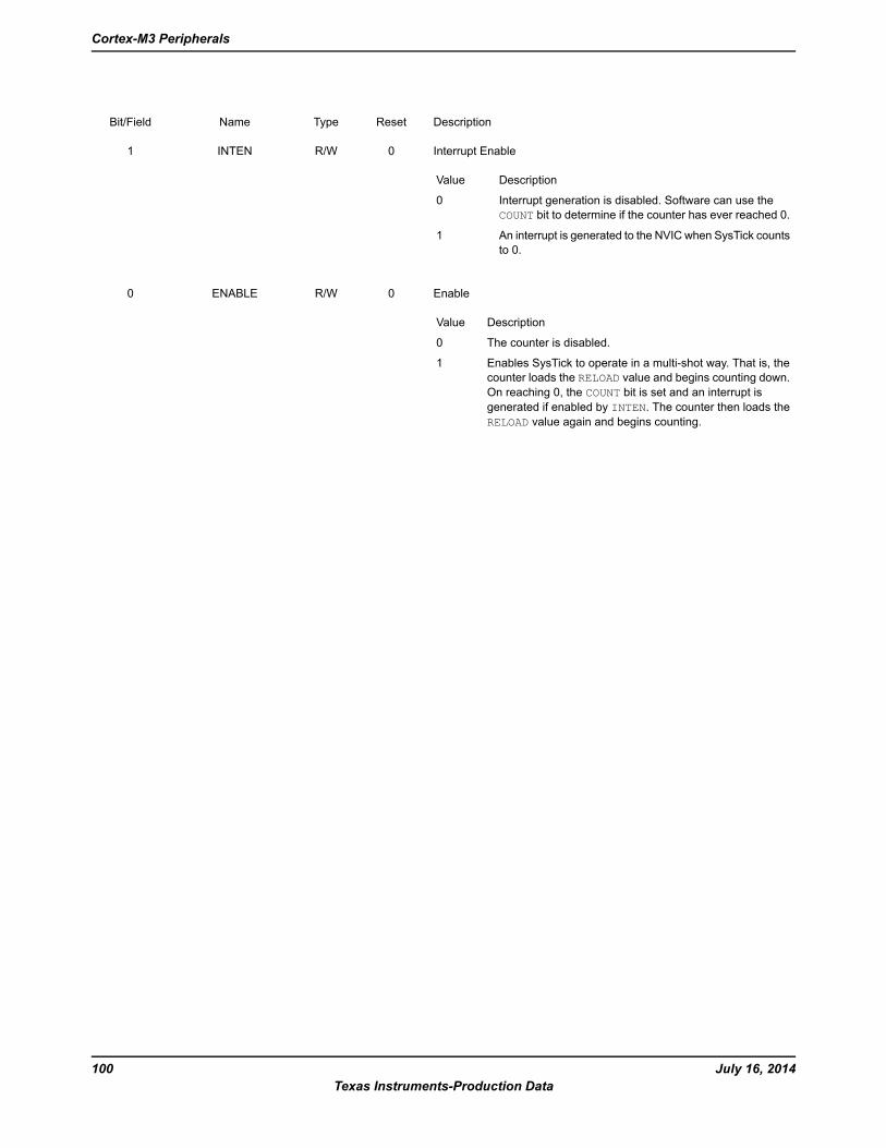
DescriptionResetTypeNameBit/Field
Interrupt Enable
DescriptionValue
Interrupt generation is disabled. Software can use theCOUNT bit to determine if the counter has ever reached 0.
0
An interrupt is generated to the NVIC when SysTick countsto 0.
1
0R/WINTEN1
Enable
DescriptionValue
The counter is disabled.0
Enables SysTick to operate in a multi-shot way. That is, thecounter loads the RELOAD value and begins counting down.On reaching 0, the COUNT bit is set and an interrupt isgenerated if enabled by INTEN. The counter then loads theRELOAD value again and begins counting.
1
0R/WENABLE0
July 16, 2014100Texas Instruments-Production Data
Cortex-M3 Peripherals
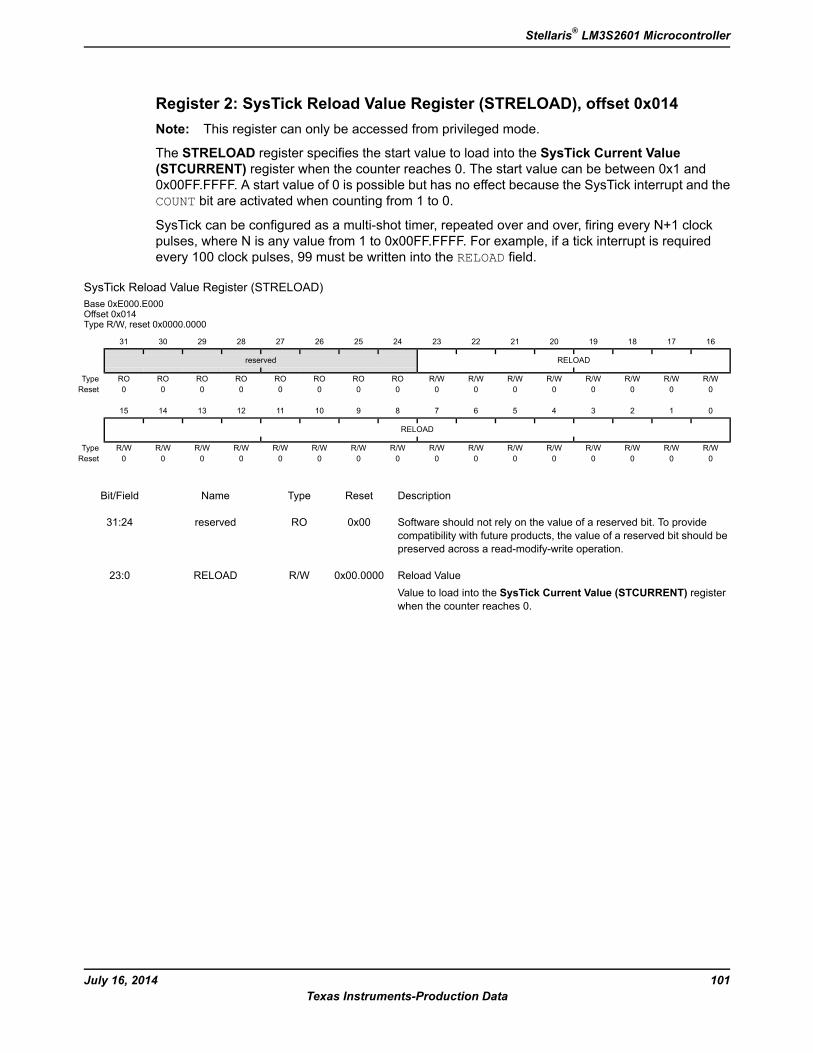
Register 2: SysTick Reload Value Register (STRELOAD), offset 0x014Note: This register can only be accessed from privileged mode.
The STRELOAD register specifies the start value to load into the SysTick Current Value(STCURRENT) register when the counter reaches 0. The start value can be between 0x1 and0x00FF.FFFF. A start value of 0 is possible but has no effect because the SysTick interrupt and theCOUNT bit are activated when counting from 1 to 0.
SysTick can be configured as a multi-shot timer, repeated over and over, firing every N+1 clockpulses, where N is any value from 1 to 0x00FF.FFFF. For example, if a tick interrupt is requiredevery 100 clock pulses, 99 must be written into the RELOAD field.
SysTick Reload Value Register (STRELOAD)Base 0xE000.E000Offset 0x014Type R/W, reset 0x0000.0000
16171819202122232425262728293031
RELOADreserved
R/WR/WR/WR/WR/WR/WR/WR/WROROROROROROROROType0000000000000000Reset
0123456789101112131415
RELOAD
R/WR/WR/WR/WR/WR/WR/WR/WR/WR/WR/WR/WR/WR/WR/WR/WType0000000000000000Reset
DescriptionResetTypeNameBit/Field
Software should not rely on the value of a reserved bit. To providecompatibility with future products, the value of a reserved bit should bepreserved across a read-modify-write operation.
0x00ROreserved31:24
Reload ValueValue to load into the SysTick Current Value (STCURRENT) registerwhen the counter reaches 0.
0x00.0000R/WRELOAD23:0
101July 16, 2014Texas Instruments-Production Data
Stellaris® LM3S2601 Microcontroller
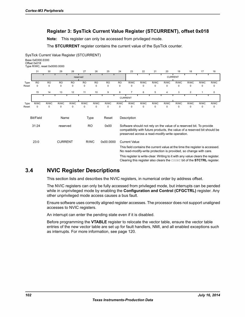
Register 3: SysTick Current Value Register (STCURRENT), offset 0x018Note: This register can only be accessed from privileged mode.
The STCURRENT register contains the current value of the SysTick counter.
SysTick Current Value Register (STCURRENT)Base 0xE000.E000Offset 0x018Type R/WC, reset 0x0000.0000
16171819202122232425262728293031
CURRENTreserved
R/WCR/WCR/WCR/WCR/WCR/WCR/WCR/WCROROROROROROROROType0000000000000000Reset
0123456789101112131415
CURRENT
R/WCR/WCR/WCR/WCR/WCR/WCR/WCR/WCR/WCR/WCR/WCR/WCR/WCR/WCR/WCR/WCType0000000000000000Reset
DescriptionResetTypeNameBit/Field
Software should not rely on the value of a reserved bit. To providecompatibility with future products, the value of a reserved bit should bepreserved across a read-modify-write operation.
0x00ROreserved31:24
Current ValueThis field contains the current value at the time the register is accessed.No read-modify-write protection is provided, so change with care.This register is write-clear. Writing to it with any value clears the register.Clearing this register also clears the COUNT bit of the STCTRL register.
0x00.0000R/WCCURRENT23:0
3.4 NVIC Register DescriptionsThis section lists and describes the NVIC registers, in numerical order by address offset.
The NVIC registers can only be fully accessed from privileged mode, but interrupts can be pendedwhile in unprivileged mode by enabling the Configuration and Control (CFGCTRL) register. Anyother unprivileged mode access causes a bus fault.
Ensure software uses correctly aligned register accesses. The processor does not support unalignedaccesses to NVIC registers.
An interrupt can enter the pending state even if it is disabled.
Before programming the VTABLE register to relocate the vector table, ensure the vector tableentries of the new vector table are set up for fault handlers, NMI, and all enabled exceptions suchas interrupts. For more information, see page 120.
July 16, 2014102Texas Instruments-Production Data
Cortex-M3 Peripherals
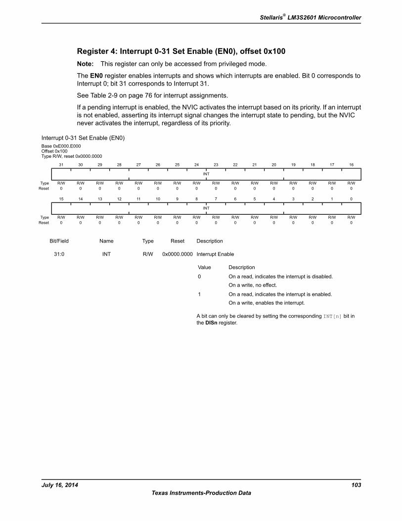
Register 4: Interrupt 0-31 Set Enable (EN0), offset 0x100Note: This register can only be accessed from privileged mode.
The EN0 register enables interrupts and shows which interrupts are enabled. Bit 0 corresponds toInterrupt 0; bit 31 corresponds to Interrupt 31.
See Table 2-9 on page 76 for interrupt assignments.
If a pending interrupt is enabled, the NVIC activates the interrupt based on its priority. If an interruptis not enabled, asserting its interrupt signal changes the interrupt state to pending, but the NVICnever activates the interrupt, regardless of its priority.
Interrupt 0-31 Set Enable (EN0)Base 0xE000.E000Offset 0x100Type R/W, reset 0x0000.0000
16171819202122232425262728293031
INT
R/WR/WR/WR/WR/WR/WR/WR/WR/WR/WR/WR/WR/WR/WR/WR/WType0000000000000000Reset
0123456789101112131415
INT
R/WR/WR/WR/WR/WR/WR/WR/WR/WR/WR/WR/WR/WR/WR/WR/WType0000000000000000Reset
DescriptionResetTypeNameBit/Field
Interrupt Enable
DescriptionValue
On a read, indicates the interrupt is disabled.On a write, no effect.
0
On a read, indicates the interrupt is enabled.On a write, enables the interrupt.
1
A bit can only be cleared by setting the corresponding INT[n] bit inthe DISn register.
0x0000.0000R/WINT31:0
103July 16, 2014Texas Instruments-Production Data
Stellaris® LM3S2601 Microcontroller
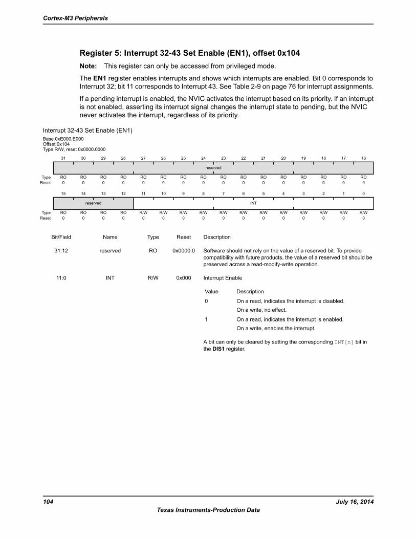
Register 5: Interrupt 32-43 Set Enable (EN1), offset 0x104Note: This register can only be accessed from privileged mode.
The EN1 register enables interrupts and shows which interrupts are enabled. Bit 0 corresponds toInterrupt 32; bit 11 corresponds to Interrupt 43. See Table 2-9 on page 76 for interrupt assignments.
If a pending interrupt is enabled, the NVIC activates the interrupt based on its priority. If an interruptis not enabled, asserting its interrupt signal changes the interrupt state to pending, but the NVICnever activates the interrupt, regardless of its priority.
Interrupt 32-43 Set Enable (EN1)Base 0xE000.E000Offset 0x104Type R/W, reset 0x0000.0000
16171819202122232425262728293031
reserved
ROROROROROROROROROROROROROROROROType0000000000000000Reset
0123456789101112131415
INTreserved
R/WR/WR/WR/WR/WR/WR/WR/WR/WR/WR/WR/WROROROROType0000000000000000Reset
DescriptionResetTypeNameBit/Field
Software should not rely on the value of a reserved bit. To providecompatibility with future products, the value of a reserved bit should bepreserved across a read-modify-write operation.
0x0000.0ROreserved31:12
Interrupt Enable
DescriptionValue
On a read, indicates the interrupt is disabled.On a write, no effect.
0
On a read, indicates the interrupt is enabled.On a write, enables the interrupt.
1
A bit can only be cleared by setting the corresponding INT[n] bit inthe DIS1 register.
0x000R/WINT11:0
July 16, 2014104Texas Instruments-Production Data
Cortex-M3 Peripherals
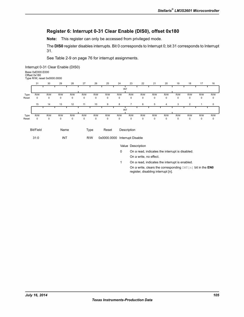
Register 6: Interrupt 0-31 Clear Enable (DIS0), offset 0x180Note: This register can only be accessed from privileged mode.
TheDIS0 register disables interrupts. Bit 0 corresponds to Interrupt 0; bit 31 corresponds to Interrupt31.
See Table 2-9 on page 76 for interrupt assignments.
Interrupt 0-31 Clear Enable (DIS0)Base 0xE000.E000Offset 0x180Type R/W, reset 0x0000.0000
16171819202122232425262728293031
INT
R/WR/WR/WR/WR/WR/WR/WR/WR/WR/WR/WR/WR/WR/WR/WR/WType0000000000000000Reset
0123456789101112131415
INT
R/WR/WR/WR/WR/WR/WR/WR/WR/WR/WR/WR/WR/WR/WR/WR/WType0000000000000000Reset
DescriptionResetTypeNameBit/Field
Interrupt Disable
DescriptionValue
On a read, indicates the interrupt is disabled.On a write, no effect.
0
On a read, indicates the interrupt is enabled.On a write, clears the corresponding INT[n] bit in the EN0register, disabling interrupt [n].
1
0x0000.0000R/WINT31:0
105July 16, 2014Texas Instruments-Production Data
Stellaris® LM3S2601 Microcontroller
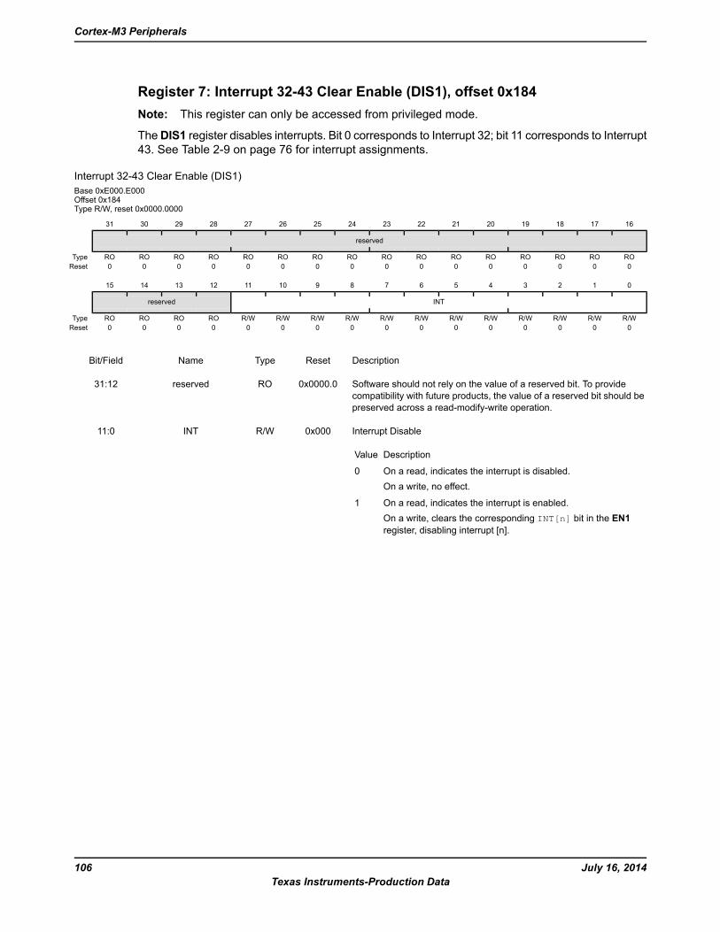
Register 7: Interrupt 32-43 Clear Enable (DIS1), offset 0x184Note: This register can only be accessed from privileged mode.
TheDIS1 register disables interrupts. Bit 0 corresponds to Interrupt 32; bit 11 corresponds to Interrupt43. See Table 2-9 on page 76 for interrupt assignments.
Interrupt 32-43 Clear Enable (DIS1)Base 0xE000.E000Offset 0x184Type R/W, reset 0x0000.0000
16171819202122232425262728293031
reserved
ROROROROROROROROROROROROROROROROType0000000000000000Reset
0123456789101112131415
INTreserved
R/WR/WR/WR/WR/WR/WR/WR/WR/WR/WR/WR/WROROROROType0000000000000000Reset
DescriptionResetTypeNameBit/Field
Software should not rely on the value of a reserved bit. To providecompatibility with future products, the value of a reserved bit should bepreserved across a read-modify-write operation.
0x0000.0ROreserved31:12
Interrupt Disable
DescriptionValue
On a read, indicates the interrupt is disabled.On a write, no effect.
0
On a read, indicates the interrupt is enabled.On a write, clears the corresponding INT[n] bit in the EN1register, disabling interrupt [n].
1
0x000R/WINT11:0
July 16, 2014106Texas Instruments-Production Data
Cortex-M3 Peripherals
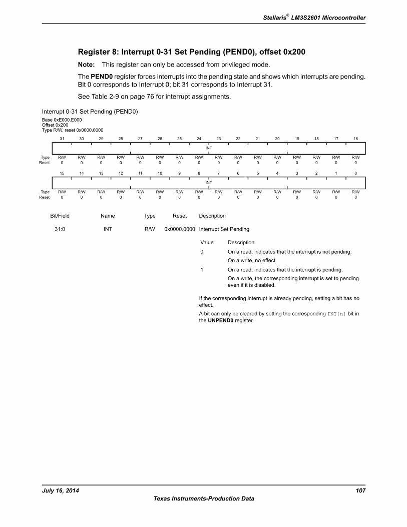
Register 8: Interrupt 0-31 Set Pending (PEND0), offset 0x200Note: This register can only be accessed from privileged mode.
The PEND0 register forces interrupts into the pending state and shows which interrupts are pending.Bit 0 corresponds to Interrupt 0; bit 31 corresponds to Interrupt 31.
See Table 2-9 on page 76 for interrupt assignments.
Interrupt 0-31 Set Pending (PEND0)Base 0xE000.E000Offset 0x200Type R/W, reset 0x0000.0000
16171819202122232425262728293031
INT
R/WR/WR/WR/WR/WR/WR/WR/WR/WR/WR/WR/WR/WR/WR/WR/WType0000000000000000Reset
0123456789101112131415
INT
R/WR/WR/WR/WR/WR/WR/WR/WR/WR/WR/WR/WR/WR/WR/WR/WType0000000000000000Reset
DescriptionResetTypeNameBit/Field
Interrupt Set Pending
DescriptionValue
On a read, indicates that the interrupt is not pending.On a write, no effect.
0
On a read, indicates that the interrupt is pending.On a write, the corresponding interrupt is set to pendingeven if it is disabled.
1
If the corresponding interrupt is already pending, setting a bit has noeffect.A bit can only be cleared by setting the corresponding INT[n] bit inthe UNPEND0 register.
0x0000.0000R/WINT31:0
107July 16, 2014Texas Instruments-Production Data
Stellaris® LM3S2601 Microcontroller
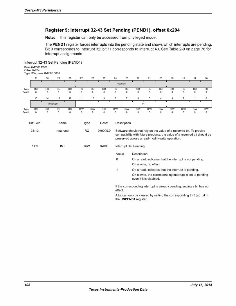
Register 9: Interrupt 32-43 Set Pending (PEND1), offset 0x204Note: This register can only be accessed from privileged mode.
The PEND1 register forces interrupts into the pending state and shows which interrupts are pending.Bit 0 corresponds to Interrupt 32; bit 11 corresponds to Interrupt 43. See Table 2-9 on page 76 forinterrupt assignments.
Interrupt 32-43 Set Pending (PEND1)Base 0xE000.E000Offset 0x204Type R/W, reset 0x0000.0000
16171819202122232425262728293031
reserved
ROROROROROROROROROROROROROROROROType0000000000000000Reset
0123456789101112131415
INTreserved
R/WR/WR/WR/WR/WR/WR/WR/WR/WR/WR/WR/WROROROROType0000000000000000Reset
DescriptionResetTypeNameBit/Field
Software should not rely on the value of a reserved bit. To providecompatibility with future products, the value of a reserved bit should bepreserved across a read-modify-write operation.
0x0000.0ROreserved31:12
Interrupt Set Pending
DescriptionValue
On a read, indicates that the interrupt is not pending.On a write, no effect.
0
On a read, indicates that the interrupt is pending.On a write, the corresponding interrupt is set to pendingeven if it is disabled.
1
If the corresponding interrupt is already pending, setting a bit has noeffect.A bit can only be cleared by setting the corresponding INT[n] bit inthe UNPEND1 register.
0x000R/WINT11:0
July 16, 2014108Texas Instruments-Production Data
Cortex-M3 Peripherals
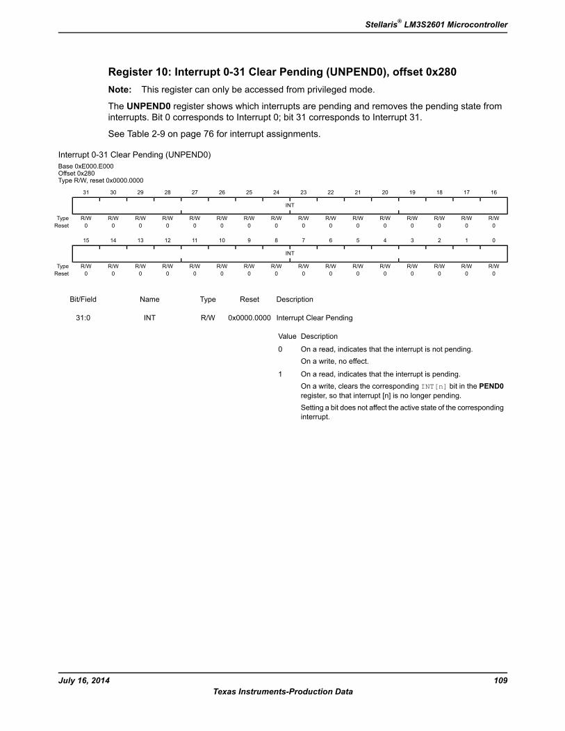
Register 10: Interrupt 0-31 Clear Pending (UNPEND0), offset 0x280Note: This register can only be accessed from privileged mode.
The UNPEND0 register shows which interrupts are pending and removes the pending state frominterrupts. Bit 0 corresponds to Interrupt 0; bit 31 corresponds to Interrupt 31.
See Table 2-9 on page 76 for interrupt assignments.
Interrupt 0-31 Clear Pending (UNPEND0)Base 0xE000.E000Offset 0x280Type R/W, reset 0x0000.0000
16171819202122232425262728293031
INT
R/WR/WR/WR/WR/WR/WR/WR/WR/WR/WR/WR/WR/WR/WR/WR/WType0000000000000000Reset
0123456789101112131415
INT
R/WR/WR/WR/WR/WR/WR/WR/WR/WR/WR/WR/WR/WR/WR/WR/WType0000000000000000Reset
DescriptionResetTypeNameBit/Field
Interrupt Clear Pending
DescriptionValue
On a read, indicates that the interrupt is not pending.On a write, no effect.
0
On a read, indicates that the interrupt is pending.On a write, clears the corresponding INT[n] bit in the PEND0register, so that interrupt [n] is no longer pending.Setting a bit does not affect the active state of the correspondinginterrupt.
1
0x0000.0000R/WINT31:0
109July 16, 2014Texas Instruments-Production Data
Stellaris® LM3S2601 Microcontroller
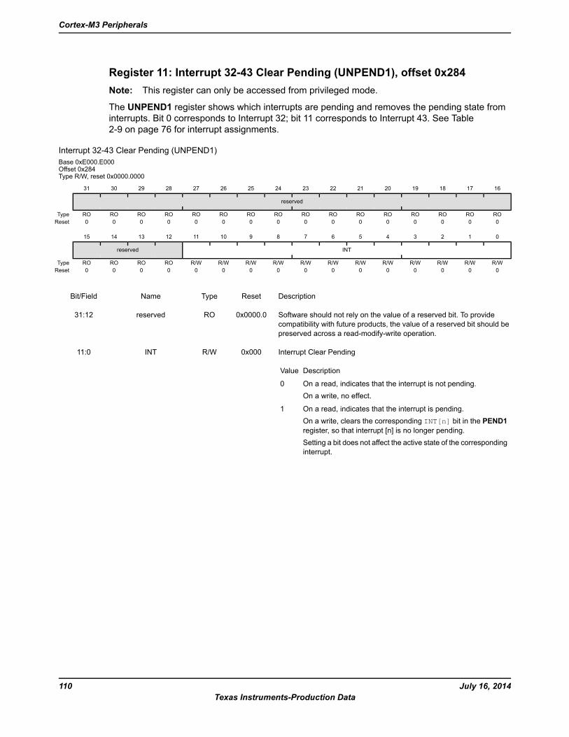
Register 11: Interrupt 32-43 Clear Pending (UNPEND1), offset 0x284Note: This register can only be accessed from privileged mode.
The UNPEND1 register shows which interrupts are pending and removes the pending state frominterrupts. Bit 0 corresponds to Interrupt 32; bit 11 corresponds to Interrupt 43. See Table2-9 on page 76 for interrupt assignments.
Interrupt 32-43 Clear Pending (UNPEND1)Base 0xE000.E000Offset 0x284Type R/W, reset 0x0000.0000
16171819202122232425262728293031
reserved
ROROROROROROROROROROROROROROROROType0000000000000000Reset
0123456789101112131415
INTreserved
R/WR/WR/WR/WR/WR/WR/WR/WR/WR/WR/WR/WROROROROType0000000000000000Reset
DescriptionResetTypeNameBit/Field
Software should not rely on the value of a reserved bit. To providecompatibility with future products, the value of a reserved bit should bepreserved across a read-modify-write operation.
0x0000.0ROreserved31:12
Interrupt Clear Pending
DescriptionValue
On a read, indicates that the interrupt is not pending.On a write, no effect.
0
On a read, indicates that the interrupt is pending.On a write, clears the corresponding INT[n] bit in the PEND1register, so that interrupt [n] is no longer pending.Setting a bit does not affect the active state of the correspondinginterrupt.
1
0x000R/WINT11:0
July 16, 2014110Texas Instruments-Production Data
Cortex-M3 Peripherals
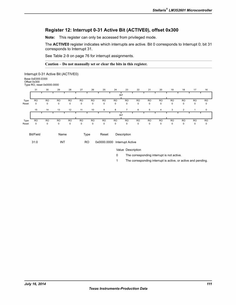
Register 12: Interrupt 0-31 Active Bit (ACTIVE0), offset 0x300Note: This register can only be accessed from privileged mode.
The ACTIVE0 register indicates which interrupts are active. Bit 0 corresponds to Interrupt 0; bit 31corresponds to Interrupt 31.
See Table 2-9 on page 76 for interrupt assignments.
Caution – Do not manually set or clear the bits in this register.
Interrupt 0-31 Active Bit (ACTIVE0)Base 0xE000.E000Offset 0x300Type RO, reset 0x0000.0000
16171819202122232425262728293031
INT
ROROROROROROROROROROROROROROROROType0000000000000000Reset
0123456789101112131415
INT
ROROROROROROROROROROROROROROROROType0000000000000000Reset
DescriptionResetTypeNameBit/Field
Interrupt Active
DescriptionValue
The corresponding interrupt is not active.0
The corresponding interrupt is active, or active and pending.1
0x0000.0000ROINT31:0
111July 16, 2014Texas Instruments-Production Data
Stellaris® LM3S2601 Microcontroller
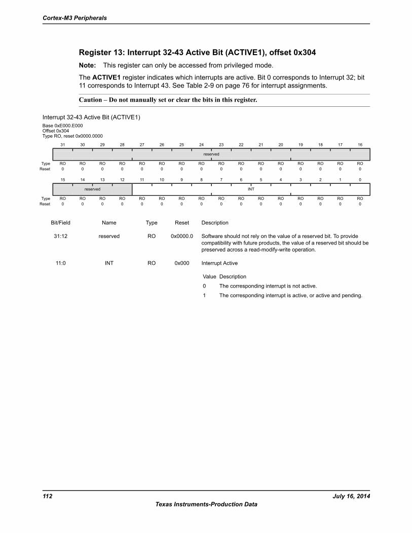
Register 13: Interrupt 32-43 Active Bit (ACTIVE1), offset 0x304Note: This register can only be accessed from privileged mode.
The ACTIVE1 register indicates which interrupts are active. Bit 0 corresponds to Interrupt 32; bit11 corresponds to Interrupt 43. See Table 2-9 on page 76 for interrupt assignments.
Caution – Do not manually set or clear the bits in this register.
Interrupt 32-43 Active Bit (ACTIVE1)Base 0xE000.E000Offset 0x304Type RO, reset 0x0000.0000
16171819202122232425262728293031
reserved
ROROROROROROROROROROROROROROROROType0000000000000000Reset
0123456789101112131415
INTreserved
ROROROROROROROROROROROROROROROROType0000000000000000Reset
DescriptionResetTypeNameBit/Field
Software should not rely on the value of a reserved bit. To providecompatibility with future products, the value of a reserved bit should bepreserved across a read-modify-write operation.
0x0000.0ROreserved31:12
Interrupt Active
DescriptionValue
The corresponding interrupt is not active.0
The corresponding interrupt is active, or active and pending.1
0x000ROINT11:0
July 16, 2014112Texas Instruments-Production Data
Cortex-M3 Peripherals
Register 14: Interrupt 0-3 Priority (PRI0), offset 0x400Register 15: Interrupt 4-7 Priority (PRI1), offset 0x404Register 16: Interrupt 8-11 Priority (PRI2), offset 0x408Register 17: Interrupt 12-15 Priority (PRI3), offset 0x40CRegister 18: Interrupt 16-19 Priority (PRI4), offset 0x410Register 19: Interrupt 20-23 Priority (PRI5), offset 0x414Register 20: Interrupt 24-27 Priority (PRI6), offset 0x418Register 21: Interrupt 28-31 Priority (PRI7), offset 0x41CRegister 22: Interrupt 32-35 Priority (PRI8), offset 0x420Register 23: Interrupt 36-39 Priority (PRI9), offset 0x424Register 24: Interrupt 40-43 Priority (PRI10), offset 0x428Note: This register can only be accessed from privileged mode.
The PRIn registers provide 3-bit priority fields for each interrupt. These registers are byte accessible.Each register holds four priority fields that are assigned to interrupts as follows:
InterruptPRIn Register Bit Field
Interrupt [4n+3]Bits 31:29
Interrupt [4n+2]Bits 23:21
Interrupt [4n+1]Bits 15:13
Interrupt [4n]Bits 7:5
See Table 2-9 on page 76 for interrupt assignments.
Each priority level can be split into separate group priority and subpriority fields. The PRIGROUPfield in the Application Interrupt and Reset Control (APINT) register (see page 121) indicates theposition of the binary point that splits the priority and subpriority fields.
These registers can only be accessed from privileged mode.
Interrupt 0-3 Priority (PRI0)Base 0xE000.E000Offset 0x400Type R/W, reset 0x0000.0000
16171819202122232425262728293031
reservedINTCreservedINTD
ROROROROROR/WR/WR/WROROROROROR/WR/WR/WType0000000000000000Reset
0123456789101112131415
reservedINTAreservedINTB
ROROROROROR/WR/WR/WROROROROROR/WR/WR/WType0000000000000000Reset
113July 16, 2014Texas Instruments-Production Data
Stellaris® LM3S2601 Microcontroller
DescriptionResetTypeNameBit/Field
Interrupt Priority for Interrupt [4n+3]This field holds a priority value, 0-7, for the interrupt with the number[4n+3], where n is the number of the Interrupt Priority register (n=0 forPRI0, and so on). The lower the value, the greater the priority of thecorresponding interrupt.
0x0R/WINTD31:29
Software should not rely on the value of a reserved bit. To providecompatibility with future products, the value of a reserved bit should bepreserved across a read-modify-write operation.
0x0ROreserved28:24
Interrupt Priority for Interrupt [4n+2]This field holds a priority value, 0-7, for the interrupt with the number[4n+2], where n is the number of the Interrupt Priority register (n=0 forPRI0, and so on). The lower the value, the greater the priority of thecorresponding interrupt.
0x0R/WINTC23:21
Software should not rely on the value of a reserved bit. To providecompatibility with future products, the value of a reserved bit should bepreserved across a read-modify-write operation.
0x0ROreserved20:16
Interrupt Priority for Interrupt [4n+1]This field holds a priority value, 0-7, for the interrupt with the number[4n+1], where n is the number of the Interrupt Priority register (n=0 forPRI0, and so on). The lower the value, the greater the priority of thecorresponding interrupt.
0x0R/WINTB15:13
Software should not rely on the value of a reserved bit. To providecompatibility with future products, the value of a reserved bit should bepreserved across a read-modify-write operation.
0x0ROreserved12:8
Interrupt Priority for Interrupt [4n]This field holds a priority value, 0-7, for the interrupt with the number[4n], where n is the number of the Interrupt Priority register (n=0 forPRI0, and so on). The lower the value, the greater the priority of thecorresponding interrupt.
0x0R/WINTA7:5
Software should not rely on the value of a reserved bit. To providecompatibility with future products, the value of a reserved bit should bepreserved across a read-modify-write operation.
0x0ROreserved4:0
July 16, 2014114Texas Instruments-Production Data
Cortex-M3 Peripherals
Register 25: Software Trigger Interrupt (SWTRIG), offset 0xF00Note: Only privileged software can enable unprivileged access to the SWTRIG register.
Writing an interrupt number to the SWTRIG register generates a Software Generated Interrupt (SGI).See Table 2-9 on page 76 for interrupt assignments.
When the MAINPEND bit in the Configuration and Control (CFGCTRL) register (see page 125) isset, unprivileged software can access the SWTRIG register.
Software Trigger Interrupt (SWTRIG)Base 0xE000.E000Offset 0xF00Type WO, reset 0x0000.0000
16171819202122232425262728293031
reserved
ROROROROROROROROROROROROROROROROType0000000000000000Reset
0123456789101112131415
INTIDreserved
WOWOWOWOWOWOROROROROROROROROROROType0000000000000000Reset
DescriptionResetTypeNameBit/Field
Software should not rely on the value of a reserved bit. To providecompatibility with future products, the value of a reserved bit should bepreserved across a read-modify-write operation.
0x0000.00ROreserved31:6
Interrupt IDThis field holds the interrupt ID of the required SGI. For example, a valueof 0x3 generates an interrupt on IRQ3.
0x00WOINTID5:0
3.5 System Control Block (SCB) Register DescriptionsThis section lists and describes the System Control Block (SCB) registers, in numerical order byaddress offset. The SCB registers can only be accessed from privileged mode.
All registers must be accessed with aligned word accesses except for the FAULTSTAT andSYSPRI1-SYSPRI3 registers, which can be accessed with byte or aligned halfword or word accesses.The processor does not support unaligned accesses to system control block registers.
115July 16, 2014Texas Instruments-Production Data
Stellaris® LM3S2601 Microcontroller
Register 26: CPU ID Base (CPUID), offset 0xD00Note: This register can only be accessed from privileged mode.
The CPUID register contains the ARM® Cortex™-M3 processor part number, version, andimplementation information.
CPU ID Base (CPUID)Base 0xE000.E000Offset 0xD00Type RO, reset 0x411F.C231
16171819202122232425262728293031
CONVARIMP
ROROROROROROROROROROROROROROROROType1111100010000010Reset
0123456789101112131415
REVPARTNO
ROROROROROROROROROROROROROROROROType1000110001000011Reset
DescriptionResetTypeNameBit/Field
Implementer Code
DescriptionValue
ARM0x41
0x41ROIMP31:24
Variant Number
DescriptionValue
The rn value in the rnpn product revision identifier, for example,the 1 in r1p1.
0x1
0x1ROVAR23:20
Constant
DescriptionValue
Always reads as 0xF.0xF
0xFROCON19:16
Part Number
DescriptionValue
Cortex-M3 processor.0xC23
0xC23ROPARTNO15:4
Revision Number
DescriptionValue
The pn value in the rnpn product revision identifier, for example,the 1 in r1p1.
0x1
0x1ROREV3:0
July 16, 2014116Texas Instruments-Production Data
Cortex-M3 Peripherals
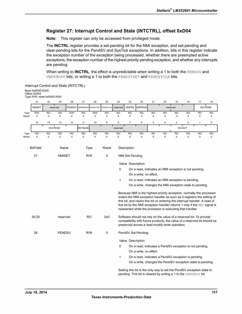
Register 27: Interrupt Control and State (INTCTRL), offset 0xD04Note: This register can only be accessed from privileged mode.
The INCTRL register provides a set-pending bit for the NMI exception, and set-pending andclear-pending bits for the PendSV and SysTick exceptions. In addition, bits in this register indicatethe exception number of the exception being processed, whether there are preempted activeexceptions, the exception number of the highest priority pending exception, and whether any interruptsare pending.
When writing to INCTRL, the effect is unpredictable when writing a 1 to both the PENDSV andUNPENDSV bits, or writing a 1 to both the PENDSTSET and PENDSTCLR bits.
Interrupt Control and State (INTCTRL)Base 0xE000.E000Offset 0xD04Type R/W, reset 0x0000.0000
16171819202122232425262728293031
VECPENDreservedISRPENDISRPREreservedPENDSTCLRPENDSTSETUNPENDSVPENDSVreservedNMISET
ROROROROROROROROROWOR/WWOR/WROROR/WType0000000000000000Reset
0123456789101112131415
VECACTreservedRETBASEVECPEND
ROROROROROROROROROROROROROROROROType0000000000000000Reset
DescriptionResetTypeNameBit/Field
NMI Set Pending
DescriptionValue
On a read, indicates an NMI exception is not pending.On a write, no effect.
0
On a read, indicates an NMI exception is pending.On a write, changes the NMI exception state to pending.
1
Because NMI is the highest-priority exception, normally the processorenters the NMI exception handler as soon as it registers the setting ofthis bit, and clears this bit on entering the interrupt handler. A read ofthis bit by the NMI exception handler returns 1 only if the NMI signal isreasserted while the processor is executing that handler.
0R/WNMISET31
Software should not rely on the value of a reserved bit. To providecompatibility with future products, the value of a reserved bit should bepreserved across a read-modify-write operation.
0x0ROreserved30:29
PendSV Set Pending
DescriptionValue
On a read, indicates a PendSV exception is not pending.On a write, no effect.
0
On a read, indicates a PendSV exception is pending.On a write, changes the PendSV exception state to pending.
1
Setting this bit is the only way to set the PendSV exception state topending. This bit is cleared by writing a 1 to the UNPENDSV bit.
0R/WPENDSV28
117July 16, 2014Texas Instruments-Production Data
Stellaris® LM3S2601 Microcontroller
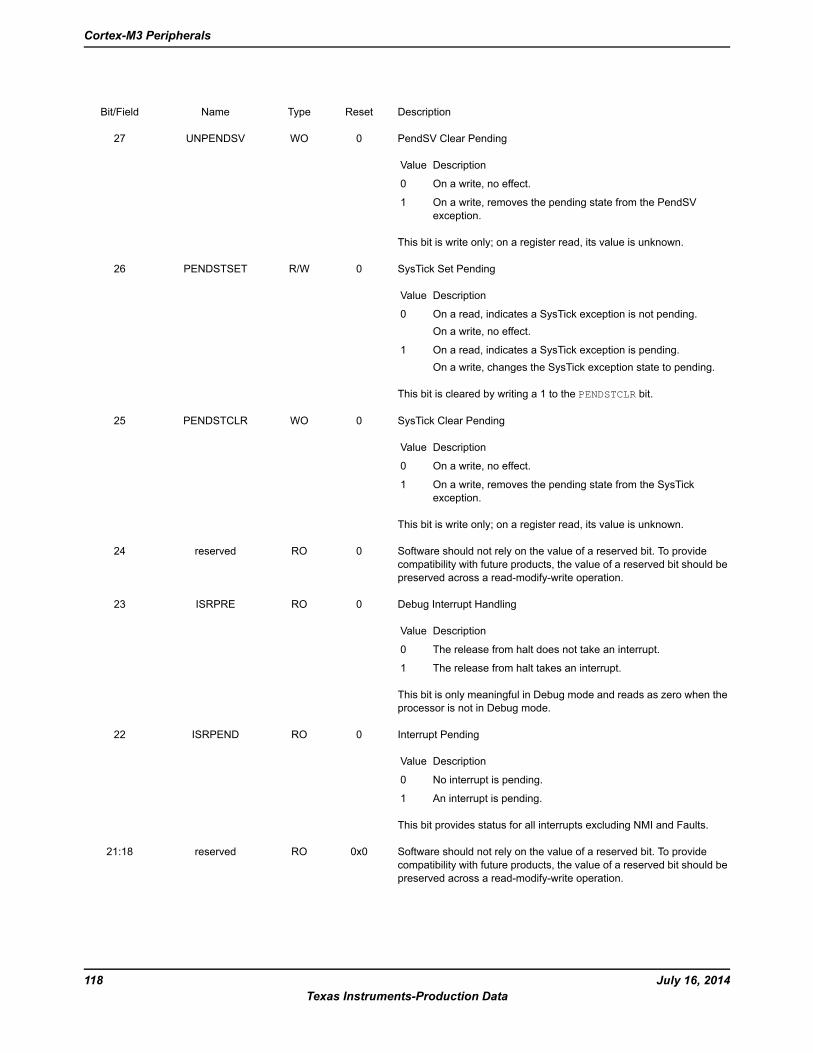
DescriptionResetTypeNameBit/Field
PendSV Clear Pending
DescriptionValue
On a write, no effect.0
On a write, removes the pending state from the PendSVexception.
1
This bit is write only; on a register read, its value is unknown.
0WOUNPENDSV27
SysTick Set Pending
DescriptionValue
On a read, indicates a SysTick exception is not pending.On a write, no effect.
0
On a read, indicates a SysTick exception is pending.On a write, changes the SysTick exception state to pending.
1
This bit is cleared by writing a 1 to the PENDSTCLR bit.
0R/WPENDSTSET26
SysTick Clear Pending
DescriptionValue
On a write, no effect.0
On a write, removes the pending state from the SysTickexception.
1
This bit is write only; on a register read, its value is unknown.
0WOPENDSTCLR25
Software should not rely on the value of a reserved bit. To providecompatibility with future products, the value of a reserved bit should bepreserved across a read-modify-write operation.
0ROreserved24
Debug Interrupt Handling
DescriptionValue
The release from halt does not take an interrupt.0
The release from halt takes an interrupt.1
This bit is only meaningful in Debug mode and reads as zero when theprocessor is not in Debug mode.
0ROISRPRE23
Interrupt Pending
DescriptionValue
No interrupt is pending.0
An interrupt is pending.1
This bit provides status for all interrupts excluding NMI and Faults.
0ROISRPEND22
Software should not rely on the value of a reserved bit. To providecompatibility with future products, the value of a reserved bit should bepreserved across a read-modify-write operation.
0x0ROreserved21:18
July 16, 2014118Texas Instruments-Production Data
Cortex-M3 Peripherals
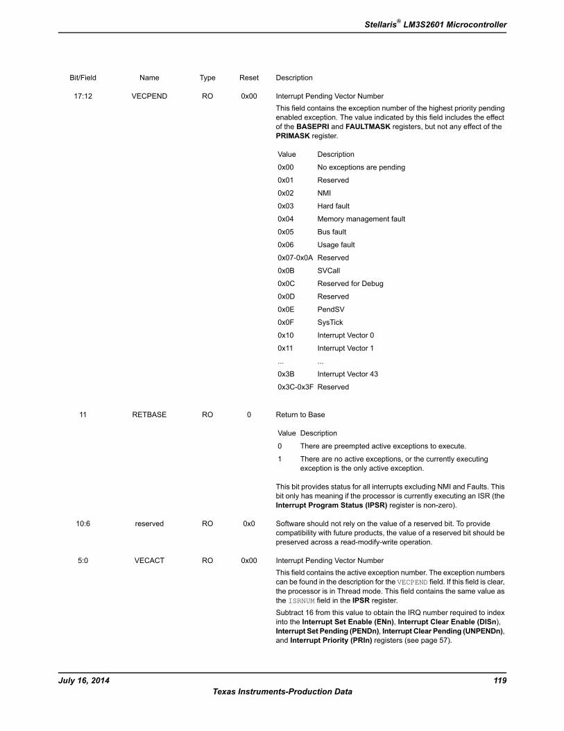
DescriptionResetTypeNameBit/Field
Interrupt Pending Vector NumberThis field contains the exception number of the highest priority pendingenabled exception. The value indicated by this field includes the effectof the BASEPRI and FAULTMASK registers, but not any effect of thePRIMASK register.
DescriptionValue
No exceptions are pending0x00
Reserved0x01
NMI0x02
Hard fault0x03
Memory management fault0x04
Bus fault0x05
Usage fault0x06
Reserved0x07-0x0A
SVCall0x0B
Reserved for Debug0x0C
Reserved0x0D
PendSV0x0E
SysTick0x0F
Interrupt Vector 00x10
Interrupt Vector 10x11
......
Interrupt Vector 430x3B
Reserved0x3C-0x3F
0x00ROVECPEND17:12
Return to Base
DescriptionValue
There are preempted active exceptions to execute.0
There are no active exceptions, or the currently executingexception is the only active exception.
1
This bit provides status for all interrupts excluding NMI and Faults. Thisbit only has meaning if the processor is currently executing an ISR (theInterrupt Program Status (IPSR) register is non-zero).
0RORETBASE11
Software should not rely on the value of a reserved bit. To providecompatibility with future products, the value of a reserved bit should bepreserved across a read-modify-write operation.
0x0ROreserved10:6
Interrupt Pending Vector NumberThis field contains the active exception number. The exception numberscan be found in the description for the VECPEND field. If this field is clear,the processor is in Thread mode. This field contains the same value asthe ISRNUM field in the IPSR register.Subtract 16 from this value to obtain the IRQ number required to indexinto the Interrupt Set Enable (ENn), Interrupt Clear Enable (DISn),Interrupt Set Pending (PENDn), Interrupt Clear Pending (UNPENDn),and Interrupt Priority (PRIn) registers (see page 57).
0x00ROVECACT5:0
119July 16, 2014Texas Instruments-Production Data
Stellaris® LM3S2601 Microcontroller
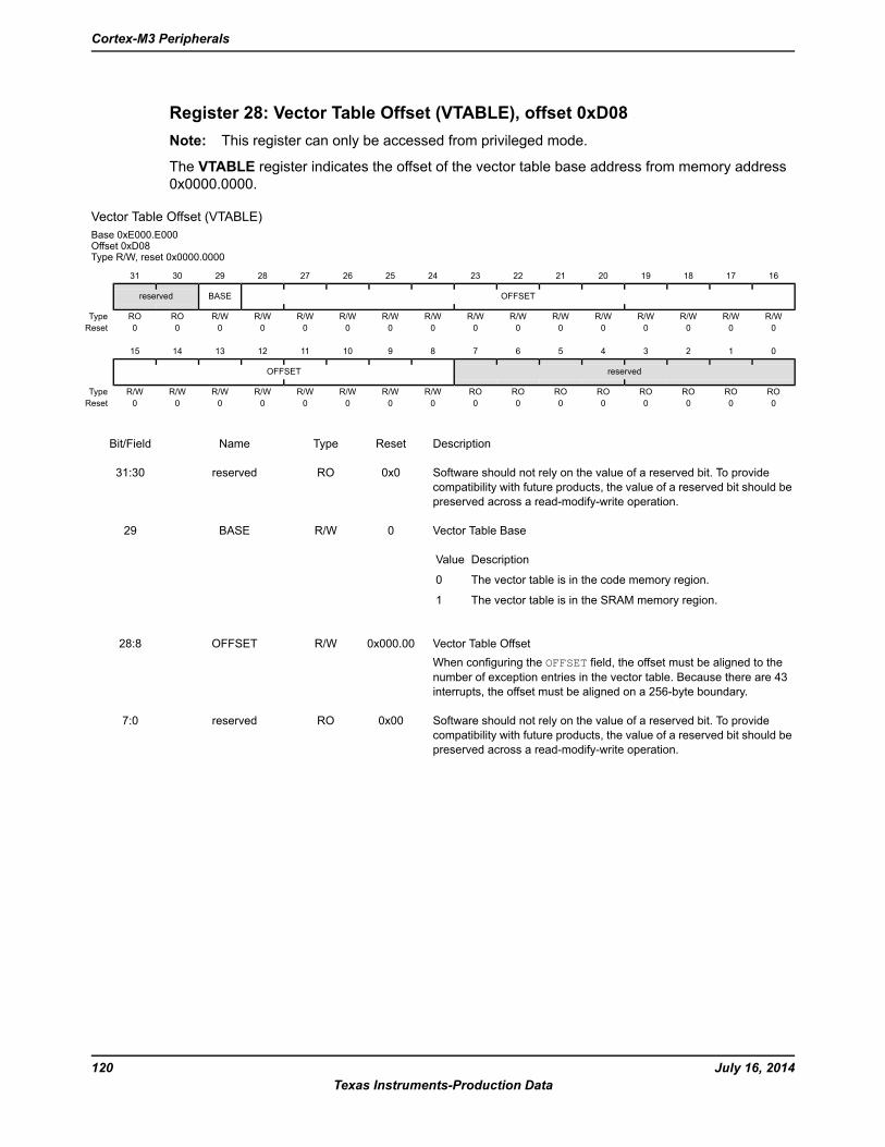
Register 28: Vector Table Offset (VTABLE), offset 0xD08Note: This register can only be accessed from privileged mode.
The VTABLE register indicates the offset of the vector table base address from memory address0x0000.0000.
Vector Table Offset (VTABLE)Base 0xE000.E000Offset 0xD08Type R/W, reset 0x0000.0000
16171819202122232425262728293031
OFFSETBASEreserved
R/WR/WR/WR/WR/WR/WR/WR/WR/WR/WR/WR/WR/WR/WROROType0000000000000000Reset
0123456789101112131415
reservedOFFSET
ROROROROROROROROR/WR/WR/WR/WR/WR/WR/WR/WType0000000000000000Reset
DescriptionResetTypeNameBit/Field
Software should not rely on the value of a reserved bit. To providecompatibility with future products, the value of a reserved bit should bepreserved across a read-modify-write operation.
0x0ROreserved31:30
Vector Table Base
DescriptionValue
The vector table is in the code memory region.0
The vector table is in the SRAM memory region.1
0R/WBASE29
Vector Table OffsetWhen configuring the OFFSET field, the offset must be aligned to thenumber of exception entries in the vector table. Because there are 43interrupts, the offset must be aligned on a 256-byte boundary.
0x000.00R/WOFFSET28:8
Software should not rely on the value of a reserved bit. To providecompatibility with future products, the value of a reserved bit should bepreserved across a read-modify-write operation.
0x00ROreserved7:0
July 16, 2014120Texas Instruments-Production Data
Cortex-M3 Peripherals
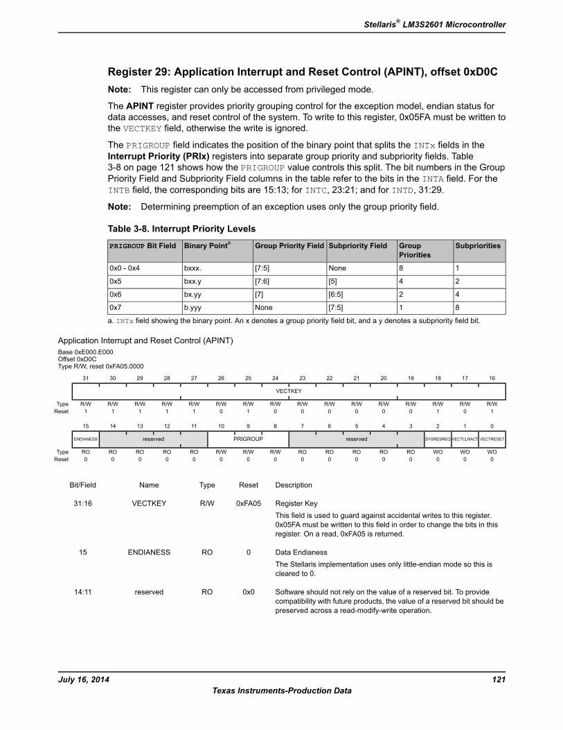
Register 29: Application Interrupt and Reset Control (APINT), offset 0xD0CNote: This register can only be accessed from privileged mode.
The APINT register provides priority grouping control for the exception model, endian status fordata accesses, and reset control of the system. To write to this register, 0x05FA must be written tothe VECTKEY field, otherwise the write is ignored.
The PRIGROUP field indicates the position of the binary point that splits the INTx fields in theInterrupt Priority (PRIx) registers into separate group priority and subpriority fields. Table3-8 on page 121 shows how the PRIGROUP value controls this split. The bit numbers in the GroupPriority Field and Subpriority Field columns in the table refer to the bits in the INTA field. For theINTB field, the corresponding bits are 15:13; for INTC, 23:21; and for INTD, 31:29.
Note: Determining preemption of an exception uses only the group priority field.
Table 3-8. Interrupt Priority Levels
SubprioritiesGroupPriorities
Subpriority FieldGroup Priority FieldBinary PointaPRIGROUP Bit Field
18None[7:5]bxxx.0x0 - 0x4
24[5][7:6]bxx.y0x5
42[6:5][7]bx.yy0x6
81[7:5]Noneb.yyy0x7
a. INTx field showing the binary point. An x denotes a group priority field bit, and a y denotes a subpriority field bit.
Application Interrupt and Reset Control (APINT)Base 0xE000.E000Offset 0xD0CType R/W, reset 0xFA05.0000
16171819202122232425262728293031
VECTKEY
R/WR/WR/WR/WR/WR/WR/WR/WR/WR/WR/WR/WR/WR/WR/WR/WType1010000001011111Reset
0123456789101112131415
VECTRESETVECTCLRACTSYSRESREQreservedPRIGROUPreservedENDIANESS
WOWOWOROROROROROR/WR/WR/WROROROROROType0000000000000000Reset
DescriptionResetTypeNameBit/Field
Register KeyThis field is used to guard against accidental writes to this register.0x05FA must be written to this field in order to change the bits in thisregister. On a read, 0xFA05 is returned.
0xFA05R/WVECTKEY31:16
Data EndianessThe Stellaris implementation uses only little-endian mode so this iscleared to 0.
0ROENDIANESS15
Software should not rely on the value of a reserved bit. To providecompatibility with future products, the value of a reserved bit should bepreserved across a read-modify-write operation.
0x0ROreserved14:11
121July 16, 2014Texas Instruments-Production Data
Stellaris® LM3S2601 Microcontroller
DescriptionResetTypeNameBit/Field
Interrupt Priority GroupingThis field determines the split of group priority from subpriority (seeTable 3-8 on page 121 for more information).
0x0R/WPRIGROUP10:8
Software should not rely on the value of a reserved bit. To providecompatibility with future products, the value of a reserved bit should bepreserved across a read-modify-write operation.
0x0ROreserved7:3
System Reset Request
DescriptionValue
No effect.0
Resets the core and all on-chip peripherals except the Debuginterface.
1
This bit is automatically cleared during the reset of the core and readsas 0.
0WOSYSRESREQ2
Clear Active NMI / FaultThis bit is reserved for Debug use and reads as 0. This bit must bewritten as a 0, otherwise behavior is unpredictable.
0WOVECTCLRACT1
System ResetThis bit is reserved for Debug use and reads as 0. This bit must bewritten as a 0, otherwise behavior is unpredictable.
0WOVECTRESET0
July 16, 2014122Texas Instruments-Production Data
Cortex-M3 Peripherals
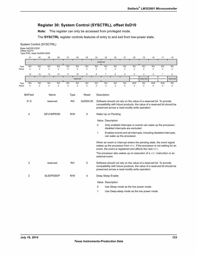
Register 30: System Control (SYSCTRL), offset 0xD10Note: This register can only be accessed from privileged mode.
The SYSCTRL register controls features of entry to and exit from low-power state.
System Control (SYSCTRL)Base 0xE000.E000Offset 0xD10Type R/W, reset 0x0000.0000
16171819202122232425262728293031
reserved
ROROROROROROROROROROROROROROROROType0000000000000000Reset
0123456789101112131415
reservedSLEEPEXITSLEEPDEEPreservedSEVONPENDreserved
ROR/WR/WROR/WROROROROROROROROROROROType0000000000000000Reset
DescriptionResetTypeNameBit/Field
Software should not rely on the value of a reserved bit. To providecompatibility with future products, the value of a reserved bit should bepreserved across a read-modify-write operation.
0x0000.00ROreserved31:5
Wake Up on Pending
DescriptionValue
Only enabled interrupts or events can wake up the processor;disabled interrupts are excluded.
0
Enabled events and all interrupts, including disabled interrupts,can wake up the processor.
1
When an event or interrupt enters the pending state, the event signalwakes up the processor from WFE. If the processor is not waiting for anevent, the event is registered and affects the next WFE.The processor also wakes up on execution of a SEV instruction or anexternal event.
0R/WSEVONPEND4
Software should not rely on the value of a reserved bit. To providecompatibility with future products, the value of a reserved bit should bepreserved across a read-modify-write operation.
0ROreserved3
Deep Sleep Enable
DescriptionValue
Use Sleep mode as the low power mode.0
Use Deep-sleep mode as the low power mode.1
0R/WSLEEPDEEP2
123July 16, 2014Texas Instruments-Production Data
Stellaris® LM3S2601 Microcontroller
DescriptionResetTypeNameBit/Field
Sleep on ISR Exit
DescriptionValue
When returning from Handler mode to Thread mode, do notsleep when returning to Thread mode.
0
When returning fromHandler mode to Threadmode, enter sleepor deep sleep on return from an ISR.
1
Setting this bit enables an interrupt-driven application to avoid returningto an empty main application.
0R/WSLEEPEXIT1
Software should not rely on the value of a reserved bit. To providecompatibility with future products, the value of a reserved bit should bepreserved across a read-modify-write operation.
0ROreserved0
July 16, 2014124Texas Instruments-Production Data
Cortex-M3 Peripherals
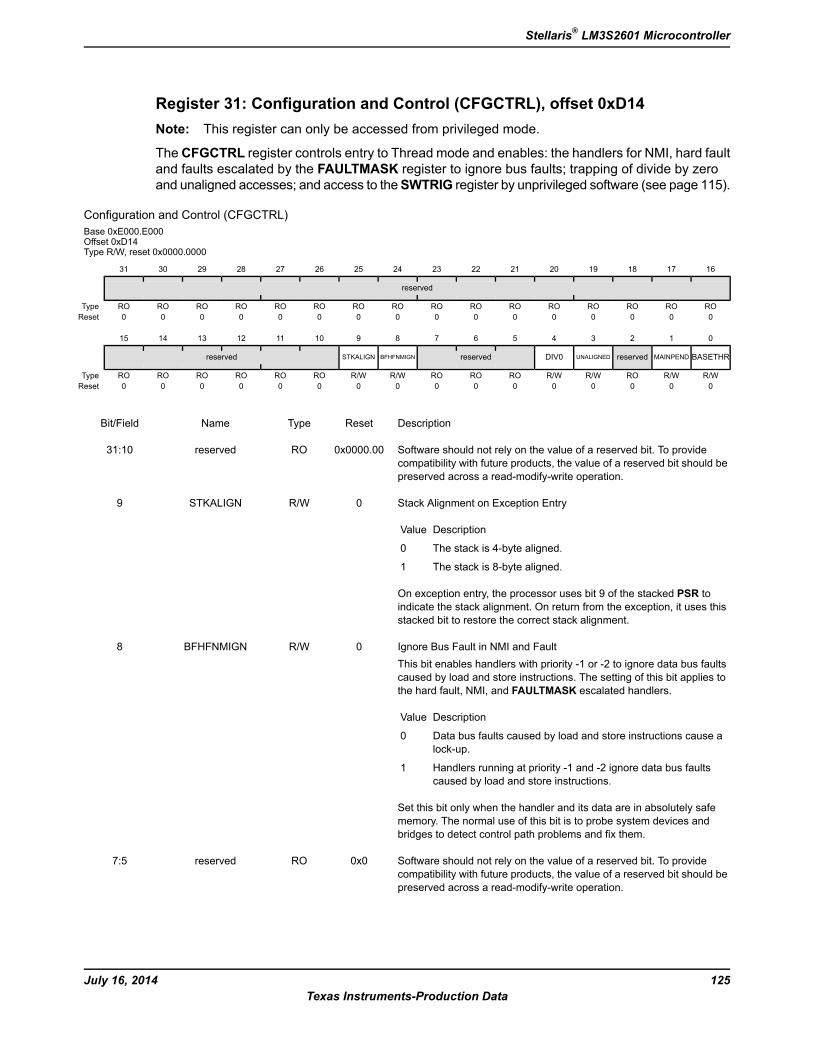
Register 31: Configuration and Control (CFGCTRL), offset 0xD14Note: This register can only be accessed from privileged mode.
The CFGCTRL register controls entry to Thread mode and enables: the handlers for NMI, hard faultand faults escalated by the FAULTMASK register to ignore bus faults; trapping of divide by zeroand unaligned accesses; and access to theSWTRIG register by unprivileged software (see page 115).
Configuration and Control (CFGCTRL)Base 0xE000.E000Offset 0xD14Type R/W, reset 0x0000.0000
16171819202122232425262728293031
reserved
ROROROROROROROROROROROROROROROROType0000000000000000Reset
0123456789101112131415
BASETHRMAINPENDreservedUNALIGNEDDIV0reservedBFHFNMIGNSTKALIGNreserved
R/WR/WROR/WR/WROROROR/WR/WROROROROROROType0000000000000000Reset
DescriptionResetTypeNameBit/Field
Software should not rely on the value of a reserved bit. To providecompatibility with future products, the value of a reserved bit should bepreserved across a read-modify-write operation.
0x0000.00ROreserved31:10
Stack Alignment on Exception Entry
DescriptionValue
The stack is 4-byte aligned.0
The stack is 8-byte aligned.1
On exception entry, the processor uses bit 9 of the stacked PSR toindicate the stack alignment. On return from the exception, it uses thisstacked bit to restore the correct stack alignment.
0R/WSTKALIGN9
Ignore Bus Fault in NMI and FaultThis bit enables handlers with priority -1 or -2 to ignore data bus faultscaused by load and store instructions. The setting of this bit applies tothe hard fault, NMI, and FAULTMASK escalated handlers.
DescriptionValue
Data bus faults caused by load and store instructions cause alock-up.
0
Handlers running at priority -1 and -2 ignore data bus faultscaused by load and store instructions.
1
Set this bit only when the handler and its data are in absolutely safememory. The normal use of this bit is to probe system devices andbridges to detect control path problems and fix them.
0R/WBFHFNMIGN8
Software should not rely on the value of a reserved bit. To providecompatibility with future products, the value of a reserved bit should bepreserved across a read-modify-write operation.
0x0ROreserved7:5
125July 16, 2014Texas Instruments-Production Data
Stellaris® LM3S2601 Microcontroller
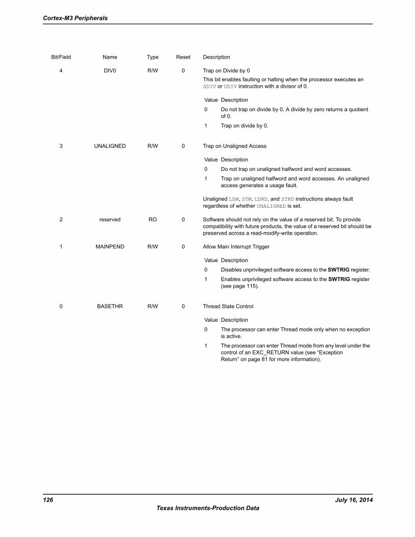
DescriptionResetTypeNameBit/Field
Trap on Divide by 0This bit enables faulting or halting when the processor executes anSDIV or UDIV instruction with a divisor of 0.
DescriptionValue
Do not trap on divide by 0. A divide by zero returns a quotientof 0.
0
Trap on divide by 0.1
0R/WDIV04
Trap on Unaligned Access
DescriptionValue
Do not trap on unaligned halfword and word accesses.0
Trap on unaligned halfword and word accesses. An unalignedaccess generates a usage fault.
1
Unaligned LDM, STM, LDRD, and STRD instructions always faultregardless of whether UNALIGNED is set.
0R/WUNALIGNED3
Software should not rely on the value of a reserved bit. To providecompatibility with future products, the value of a reserved bit should bepreserved across a read-modify-write operation.
0ROreserved2
Allow Main Interrupt Trigger
DescriptionValue
Disables unprivileged software access to the SWTRIG register.0
Enables unprivileged software access to the SWTRIG register(see page 115).
1
0R/WMAINPEND1
Thread State Control
DescriptionValue
The processor can enter Thread mode only when no exceptionis active.
0
The processor can enter Thread mode from any level under thecontrol of an EXC_RETURN value (see “ExceptionReturn” on page 81 for more information).
1
0R/WBASETHR0
July 16, 2014126Texas Instruments-Production Data
Cortex-M3 Peripherals
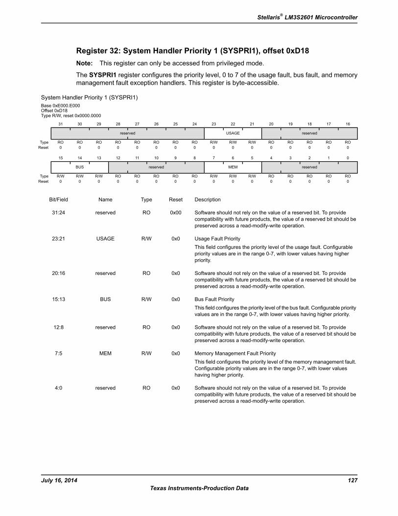
Register 32: System Handler Priority 1 (SYSPRI1), offset 0xD18Note: This register can only be accessed from privileged mode.
The SYSPRI1 register configures the priority level, 0 to 7 of the usage fault, bus fault, and memorymanagement fault exception handlers. This register is byte-accessible.
System Handler Priority 1 (SYSPRI1)Base 0xE000.E000Offset 0xD18Type R/W, reset 0x0000.0000
16171819202122232425262728293031
reservedUSAGEreserved
ROROROROROR/WR/WR/WROROROROROROROROType0000000000000000Reset
0123456789101112131415
reservedMEMreservedBUS
ROROROROROR/WR/WR/WROROROROROR/WR/WR/WType0000000000000000Reset
DescriptionResetTypeNameBit/Field
Software should not rely on the value of a reserved bit. To providecompatibility with future products, the value of a reserved bit should bepreserved across a read-modify-write operation.
0x00ROreserved31:24
Usage Fault PriorityThis field configures the priority level of the usage fault. Configurablepriority values are in the range 0-7, with lower values having higherpriority.
0x0R/WUSAGE23:21
Software should not rely on the value of a reserved bit. To providecompatibility with future products, the value of a reserved bit should bepreserved across a read-modify-write operation.
0x0ROreserved20:16
Bus Fault PriorityThis field configures the priority level of the bus fault. Configurable priorityvalues are in the range 0-7, with lower values having higher priority.
0x0R/WBUS15:13
Software should not rely on the value of a reserved bit. To providecompatibility with future products, the value of a reserved bit should bepreserved across a read-modify-write operation.
0x0ROreserved12:8
Memory Management Fault PriorityThis field configures the priority level of the memory management fault.Configurable priority values are in the range 0-7, with lower valueshaving higher priority.
0x0R/WMEM7:5
Software should not rely on the value of a reserved bit. To providecompatibility with future products, the value of a reserved bit should bepreserved across a read-modify-write operation.
0x0ROreserved4:0
127July 16, 2014Texas Instruments-Production Data
Stellaris® LM3S2601 Microcontroller
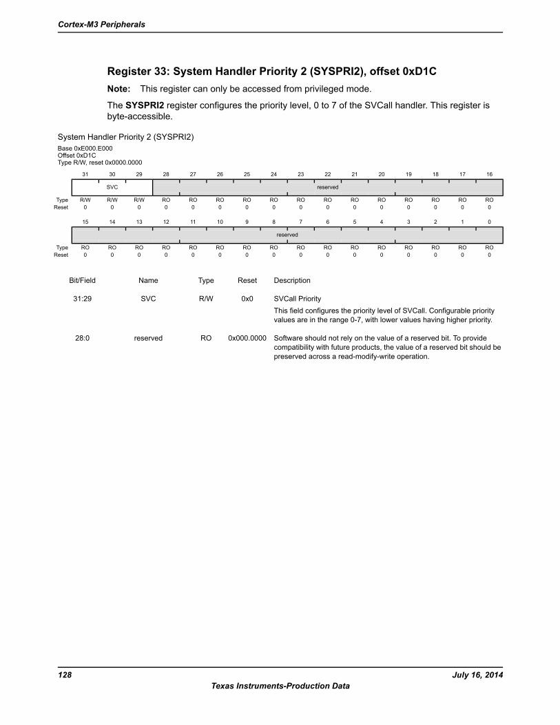
Register 33: System Handler Priority 2 (SYSPRI2), offset 0xD1CNote: This register can only be accessed from privileged mode.
The SYSPRI2 register configures the priority level, 0 to 7 of the SVCall handler. This register isbyte-accessible.
System Handler Priority 2 (SYSPRI2)Base 0xE000.E000Offset 0xD1CType R/W, reset 0x0000.0000
16171819202122232425262728293031
reservedSVC
ROROROROROROROROROROROROROR/WR/WR/WType0000000000000000Reset
0123456789101112131415
reserved
ROROROROROROROROROROROROROROROROType0000000000000000Reset
DescriptionResetTypeNameBit/Field
SVCall PriorityThis field configures the priority level of SVCall. Configurable priorityvalues are in the range 0-7, with lower values having higher priority.
0x0R/WSVC31:29
Software should not rely on the value of a reserved bit. To providecompatibility with future products, the value of a reserved bit should bepreserved across a read-modify-write operation.
0x000.0000ROreserved28:0
July 16, 2014128Texas Instruments-Production Data
Cortex-M3 Peripherals
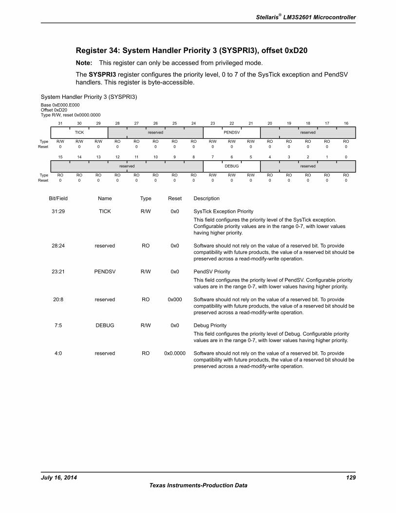
Register 34: System Handler Priority 3 (SYSPRI3), offset 0xD20Note: This register can only be accessed from privileged mode.
The SYSPRI3 register configures the priority level, 0 to 7 of the SysTick exception and PendSVhandlers. This register is byte-accessible.
System Handler Priority 3 (SYSPRI3)Base 0xE000.E000Offset 0xD20Type R/W, reset 0x0000.0000
16171819202122232425262728293031
reservedPENDSVreservedTICK
ROROROROROR/WR/WR/WROROROROROR/WR/WR/WType0000000000000000Reset
0123456789101112131415
reservedDEBUGreserved
ROROROROROR/WR/WR/WROROROROROROROROType0000000000000000Reset
DescriptionResetTypeNameBit/Field
SysTick Exception PriorityThis field configures the priority level of the SysTick exception.Configurable priority values are in the range 0-7, with lower valueshaving higher priority.
0x0R/WTICK31:29
Software should not rely on the value of a reserved bit. To providecompatibility with future products, the value of a reserved bit should bepreserved across a read-modify-write operation.
0x0ROreserved28:24
PendSV PriorityThis field configures the priority level of PendSV. Configurable priorityvalues are in the range 0-7, with lower values having higher priority.
0x0R/WPENDSV23:21
Software should not rely on the value of a reserved bit. To providecompatibility with future products, the value of a reserved bit should bepreserved across a read-modify-write operation.
0x000ROreserved20:8
Debug PriorityThis field configures the priority level of Debug. Configurable priorityvalues are in the range 0-7, with lower values having higher priority.
0x0R/WDEBUG7:5
Software should not rely on the value of a reserved bit. To providecompatibility with future products, the value of a reserved bit should bepreserved across a read-modify-write operation.
0x0.0000ROreserved4:0
129July 16, 2014Texas Instruments-Production Data
Stellaris® LM3S2601 Microcontroller
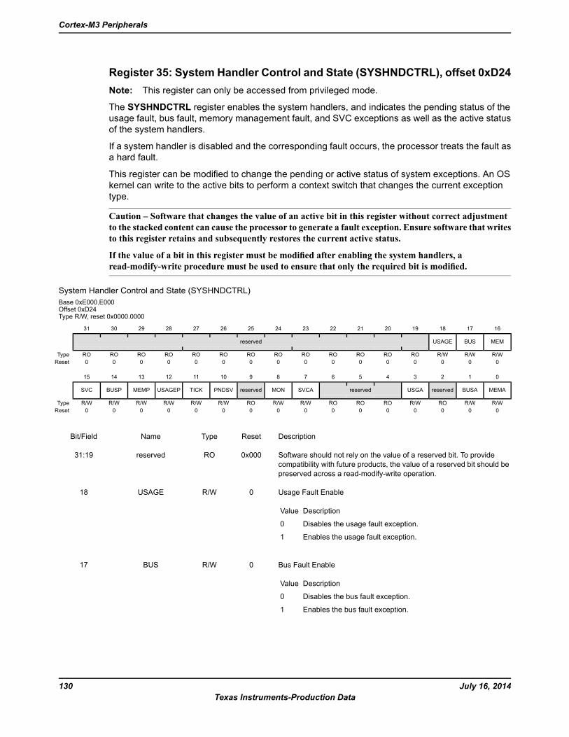
Register 35: System Handler Control and State (SYSHNDCTRL), offset 0xD24Note: This register can only be accessed from privileged mode.
The SYSHNDCTRL register enables the system handlers, and indicates the pending status of theusage fault, bus fault, memory management fault, and SVC exceptions as well as the active statusof the system handlers.
If a system handler is disabled and the corresponding fault occurs, the processor treats the fault asa hard fault.
This register can be modified to change the pending or active status of system exceptions. An OSkernel can write to the active bits to perform a context switch that changes the current exceptiontype.
Caution – Software that changes the value of an active bit in this register without correct adjustmentto the stacked content can cause the processor to generate a fault exception. Ensure software that writesto this register retains and subsequently restores the current active status.
If the value of a bit in this register must be modified after enabling the system handlers, aread-modify-write procedure must be used to ensure that only the required bit is modified.
System Handler Control and State (SYSHNDCTRL)Base 0xE000.E000Offset 0xD24Type R/W, reset 0x0000.0000
16171819202122232425262728293031
MEMBUSUSAGEreserved
R/WR/WR/WROROROROROROROROROROROROROType0000000000000000Reset
0123456789101112131415
MEMABUSAreservedUSGAreservedSVCAMONreservedPNDSVTICKUSAGEPMEMPBUSPSVC
R/WR/WROR/WROROROR/WR/WROR/WR/WR/WR/WR/WR/WType0000000000000000Reset
DescriptionResetTypeNameBit/Field
Software should not rely on the value of a reserved bit. To providecompatibility with future products, the value of a reserved bit should bepreserved across a read-modify-write operation.
0x000ROreserved31:19
Usage Fault Enable
DescriptionValue
Disables the usage fault exception.0
Enables the usage fault exception.1
0R/WUSAGE18
Bus Fault Enable
DescriptionValue
Disables the bus fault exception.0
Enables the bus fault exception.1
0R/WBUS17
July 16, 2014130Texas Instruments-Production Data
Cortex-M3 Peripherals
DescriptionResetTypeNameBit/Field
Memory Management Fault Enable
DescriptionValue
Disables the memory management fault exception.0
Enables the memory management fault exception.1
0R/WMEM16
SVC Call Pending
DescriptionValue
An SVC call exception is not pending.0
An SVC call exception is pending.1
This bit can be modified to change the pending status of the SVC callexception.
0R/WSVC15
Bus Fault Pending
DescriptionValue
A bus fault exception is not pending.0
A bus fault exception is pending.1
This bit can be modified to change the pending status of the bus faultexception.
0R/WBUSP14
Memory Management Fault Pending
DescriptionValue
A memory management fault exception is not pending.0
A memory management fault exception is pending.1
This bit can be modified to change the pending status of the memorymanagement fault exception.
0R/WMEMP13
Usage Fault Pending
DescriptionValue
A usage fault exception is not pending.0
A usage fault exception is pending.1
This bit can be modified to change the pending status of the usage faultexception.
0R/WUSAGEP12
SysTick Exception Active
DescriptionValue
A SysTick exception is not active.0
A SysTick exception is active.1
This bit can be modified to change the active status of the SysTickexception, however, see the Caution above before setting this bit.
0R/WTICK11
131July 16, 2014Texas Instruments-Production Data
Stellaris® LM3S2601 Microcontroller
DescriptionResetTypeNameBit/Field
PendSV Exception Active
DescriptionValue
A PendSV exception is not active.0
A PendSV exception is active.1
This bit can be modified to change the active status of the PendSVexception, however, see the Caution above before setting this bit.
0R/WPNDSV10
Software should not rely on the value of a reserved bit. To providecompatibility with future products, the value of a reserved bit should bepreserved across a read-modify-write operation.
0ROreserved9
Debug Monitor Active
DescriptionValue
The Debug monitor is not active.0
The Debug monitor is active.1
0R/WMON8
SVC Call Active
DescriptionValue
SVC call is not active.0
SVC call is active.1
This bit can be modified to change the active status of the SVC callexception, however, see the Caution above before setting this bit.
0R/WSVCA7
Software should not rely on the value of a reserved bit. To providecompatibility with future products, the value of a reserved bit should bepreserved across a read-modify-write operation.
0x0ROreserved6:4
Usage Fault Active
DescriptionValue
Usage fault is not active.0
Usage fault is active.1
This bit can be modified to change the active status of the usage faultexception, however, see the Caution above before setting this bit.
0R/WUSGA3
Software should not rely on the value of a reserved bit. To providecompatibility with future products, the value of a reserved bit should bepreserved across a read-modify-write operation.
0ROreserved2
Bus Fault Active
DescriptionValue
Bus fault is not active.0
Bus fault is active.1
This bit can be modified to change the active status of the bus faultexception, however, see the Caution above before setting this bit.
0R/WBUSA1
July 16, 2014132Texas Instruments-Production Data
Cortex-M3 Peripherals
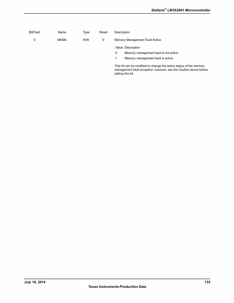
DescriptionResetTypeNameBit/Field
Memory Management Fault Active
DescriptionValue
Memory management fault is not active.0
Memory management fault is active.1
This bit can be modified to change the active status of the memorymanagement fault exception, however, see the Caution above beforesetting this bit.
0R/WMEMA0
133July 16, 2014Texas Instruments-Production Data
Stellaris® LM3S2601 Microcontroller
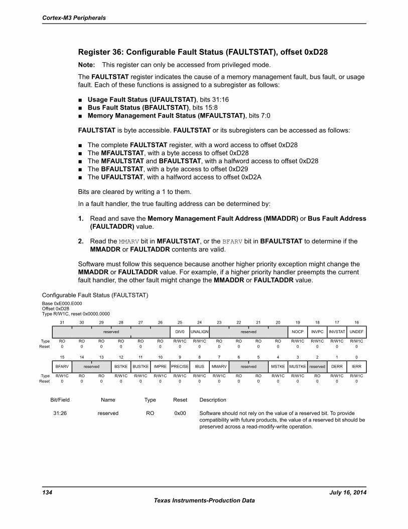
Register 36: Configurable Fault Status (FAULTSTAT), offset 0xD28Note: This register can only be accessed from privileged mode.
The FAULTSTAT register indicates the cause of a memory management fault, bus fault, or usagefault. Each of these functions is assigned to a subregister as follows:
Usage Fault Status (UFAULTSTAT), bits 31:16 Bus Fault Status (BFAULTSTAT), bits 15:8 Memory Management Fault Status (MFAULTSTAT), bits 7:0
FAULTSTAT is byte accessible. FAULTSTAT or its subregisters can be accessed as follows:
The complete FAULTSTAT register, with a word access to offset 0xD28 The MFAULTSTAT, with a byte access to offset 0xD28 The MFAULTSTAT and BFAULTSTAT, with a halfword access to offset 0xD28 The BFAULTSTAT, with a byte access to offset 0xD29 The UFAULTSTAT, with a halfword access to offset 0xD2A
Bits are cleared by writing a 1 to them.
In a fault handler, the true faulting address can be determined by:
1. Read and save the Memory Management Fault Address (MMADDR) or Bus Fault Address(FAULTADDR) value.
2. Read the MMARV bit in MFAULTSTAT, or the BFARV bit in BFAULTSTAT to determine if theMMADDR or FAULTADDR contents are valid.
Software must follow this sequence because another higher priority exception might change theMMADDR or FAULTADDR value. For example, if a higher priority handler preempts the currentfault handler, the other fault might change the MMADDR or FAULTADDR value.
Configurable Fault Status (FAULTSTAT)Base 0xE000.E000Offset 0xD28Type R/W1C, reset 0x0000.0000
16171819202122232425262728293031
UNDEFINVSTATINVPCNOCPreservedUNALIGNDIV0reserved
R/W1CR/W1CR/W1CR/W1CROROROROR/W1CR/W1CROROROROROROType0000000000000000Reset
0123456789101112131415
IERRDERRreservedMUSTKEMSTKEreservedMMARVIBUSPRECISEIMPREBUSTKEBSTKEreservedBFARV
R/W1CR/W1CROR/W1CR/W1CROROR/W1CR/W1CR/W1CR/W1CR/W1CR/W1CROROR/W1CType0000000000000000Reset
DescriptionResetTypeNameBit/Field
Software should not rely on the value of a reserved bit. To providecompatibility with future products, the value of a reserved bit should bepreserved across a read-modify-write operation.
0x00ROreserved31:26
July 16, 2014134Texas Instruments-Production Data
Cortex-M3 Peripherals
DescriptionResetTypeNameBit/Field
Divide-by-Zero Usage Fault
DescriptionValue
No divide-by-zero fault has occurred, or divide-by-zero trappingis not enabled.
0
The processor has executed an SDIV or UDIV instruction witha divisor of 0.
1
When this bit is set, the PC value stacked for the exception return pointsto the instruction that performed the divide by zero.Trapping on divide-by-zero is enabled by setting the DIV0 bit in theConfiguration and Control (CFGCTRL) register (see page 125).This bit is cleared by writing a 1 to it.
0R/W1CDIV025
Unaligned Access Usage Fault
DescriptionValue
No unaligned access fault has occurred, or unaligned accesstrapping is not enabled.
0
The processor has made an unaligned memory access.1
Unaligned LDM, STM, LDRD, and STRD instructions always faultregardless of the configuration of this bit.Trapping on unaligned access is enabled by setting the UNALIGNED bitin the CFGCTRL register (see page 125).This bit is cleared by writing a 1 to it.
0R/W1CUNALIGN24
Software should not rely on the value of a reserved bit. To providecompatibility with future products, the value of a reserved bit should bepreserved across a read-modify-write operation.
0x00ROreserved23:20
No Coprocessor Usage Fault
DescriptionValue
A usage fault has not been caused by attempting to access acoprocessor.
0
The processor has attempted to access a coprocessor.1
This bit is cleared by writing a 1 to it.
0R/W1CNOCP19
Invalid PC Load Usage Fault
DescriptionValue
A usage fault has not been caused by attempting to load aninvalid PC value.
0
The processor has attempted an illegal load of EXC_RETURNto the PC as a result of an invalid context or an invalidEXC_RETURN value.
1
When this bit is set, the PC value stacked for the exception return pointsto the instruction that tried to perform the illegal load of the PC.This bit is cleared by writing a 1 to it.
0R/W1CINVPC18
135July 16, 2014Texas Instruments-Production Data
Stellaris® LM3S2601 Microcontroller
DescriptionResetTypeNameBit/Field
Invalid State Usage Fault
DescriptionValue
A usage fault has not been caused by an invalid state.0
The processor has attempted to execute an instruction thatmakes illegal use of the EPSR register.
1
When this bit is set, the PC value stacked for the exception return pointsto the instruction that attempted the illegal use of the ExecutionProgram Status Register (EPSR) register.This bit is not set if an undefined instruction uses the EPSR register.This bit is cleared by writing a 1 to it.
0R/W1CINVSTAT17
Undefined Instruction Usage Fault
DescriptionValue
A usage fault has not been caused by an undefined instruction.0
The processor has attempted to execute an undefinedinstruction.
1
When this bit is set, the PC value stacked for the exception return pointsto the undefined instruction.An undefined instruction is an instruction that the processor cannotdecode.This bit is cleared by writing a 1 to it.
0R/W1CUNDEF16
Bus Fault Address Register Valid
DescriptionValue
The value in the Bus Fault Address (FAULTADDR) registeris not a valid fault address.
0
The FAULTADDR register is holding a valid fault address.1
This bit is set after a bus fault, where the address is known. Other faultscan clear this bit, such as a memory management fault occurring later.If a bus fault occurs and is escalated to a hard fault because of priority,the hard fault handler must clear this bit. This action prevents problemsif returning to a stacked active bus fault handler whose FAULTADDRregister value has been overwritten.This bit is cleared by writing a 1 to it.
0R/W1CBFARV15
Software should not rely on the value of a reserved bit. To providecompatibility with future products, the value of a reserved bit should bepreserved across a read-modify-write operation.
0ROreserved14:13
July 16, 2014136Texas Instruments-Production Data
Cortex-M3 Peripherals
DescriptionResetTypeNameBit/Field
Stack Bus Fault
DescriptionValue
No bus fault has occurred on stacking for exception entry.0
Stacking for an exception entry has caused one or more busfaults.
1
When this bit is set, the SP is still adjusted but the values in the contextarea on the stack might be incorrect. A fault address is not written tothe FAULTADDR register.This bit is cleared by writing a 1 to it.
0R/W1CBSTKE12
Unstack Bus Fault
DescriptionValue
No bus fault has occurred on unstacking for a return fromexception.
0
Unstacking for a return from exception has caused one or morebus faults.
1
This fault is chained to the handler. Thus, when this bit is set, the originalreturn stack is still present. The SP is not adjusted from the failing return,a new save is not performed, and a fault address is not written to theFAULTADDR register.This bit is cleared by writing a 1 to it.
0R/W1CBUSTKE11
Imprecise Data Bus Error
DescriptionValue
An imprecise data bus error has not occurred.0
A data bus error has occurred, but the return address in thestack frame is not related to the instruction that caused the error.
1
When this bit is set, a fault address is not written to the FAULTADDRregister.This fault is asynchronous. Therefore, if the fault is detected when thepriority of the current process is higher than the bus fault priority, thebus fault becomes pending and becomes active only when the processorreturns from all higher-priority processes. If a precise fault occurs beforethe processor enters the handler for the imprecise bus fault, the handlerdetects that both the IMPRE bit is set and one of the precise fault statusbits is set.This bit is cleared by writing a 1 to it.
0R/W1CIMPRE10
Precise Data Bus Error
DescriptionValue
A precise data bus error has not occurred.0
A data bus error has occurred, and the PC value stacked forthe exception return points to the instruction that caused thefault.
1
When this bit is set, the fault address is written to the FAULTADDRregister.This bit is cleared by writing a 1 to it.
0R/W1CPRECISE9
137July 16, 2014Texas Instruments-Production Data
Stellaris® LM3S2601 Microcontroller
DescriptionResetTypeNameBit/Field
Instruction Bus Error
DescriptionValue
An instruction bus error has not occurred.0
An instruction bus error has occurred.1
The processor detects the instruction bus error on prefetching aninstruction, but sets this bit only if it attempts to issue the faultinginstruction.When this bit is set, a fault address is not written to the FAULTADDRregister.This bit is cleared by writing a 1 to it.
0R/W1CIBUS8
Memory Management Fault Address Register Valid
DescriptionValue
The value in the Memory Management Fault Address(MMADDR) register is not a valid fault address.
0
The MMADDR register is holding a valid fault address.1
If a memory management fault occurs and is escalated to a hard faultbecause of priority, the hard fault handler must clear this bit. This actionprevents problems if returning to a stacked active memory managementfault handler whose MMADDR register value has been overwritten.This bit is cleared by writing a 1 to it.
0R/W1CMMARV7
Software should not rely on the value of a reserved bit. To providecompatibility with future products, the value of a reserved bit should bepreserved across a read-modify-write operation.
0ROreserved6:5
Stack Access Violation
DescriptionValue
No memory management fault has occurred on stacking forexception entry.
0
Stacking for an exception entry has caused one or more accessviolations.
1
When this bit is set, the SP is still adjusted but the values in the contextarea on the stack might be incorrect. A fault address is not written tothe MMADDR register.This bit is cleared by writing a 1 to it.
0R/W1CMSTKE4
July 16, 2014138Texas Instruments-Production Data
Cortex-M3 Peripherals
DescriptionResetTypeNameBit/Field
Unstack Access Violation
DescriptionValue
No memory management fault has occurred on unstacking fora return from exception.
0
Unstacking for a return from exception has caused one or moreaccess violations.
1
This fault is chained to the handler. Thus, when this bit is set, the originalreturn stack is still present. The SP is not adjusted from the failing return,a new save is not performed, and a fault address is not written to theMMADDR register.This bit is cleared by writing a 1 to it.
0R/W1CMUSTKE3
Software should not rely on the value of a reserved bit. To providecompatibility with future products, the value of a reserved bit should bepreserved across a read-modify-write operation.
0ROreserved2
Data Access Violation
DescriptionValue
A data access violation has not occurred.0
The processor attempted a load or store at a location that doesnot permit the operation.
1
When this bit is set, the PC value stacked for the exception return pointsto the faulting instruction and the address of the attempted access iswritten to the MMADDR register.This bit is cleared by writing a 1 to it.
0R/W1CDERR1
Instruction Access Violation
DescriptionValue
An instruction access violation has not occurred.0
The processor attempted an instruction fetch from a locationthat does not permit execution.
1
This fault occurs on any access to an XN region, even when the MPUis disabled or not present.When this bit is set, the PC value stacked for the exception return pointsto the faulting instruction and the address of the attempted access isnot written to the MMADDR register.This bit is cleared by writing a 1 to it.
0R/W1CIERR0
139July 16, 2014Texas Instruments-Production Data
Stellaris® LM3S2601 Microcontroller
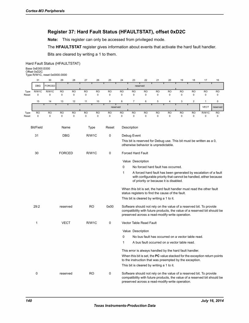
Register 37: Hard Fault Status (HFAULTSTAT), offset 0xD2CNote: This register can only be accessed from privileged mode.
The HFAULTSTAT register gives information about events that activate the hard fault handler.
Bits are cleared by writing a 1 to them.
Hard Fault Status (HFAULTSTAT)Base 0xE000.E000Offset 0xD2CType R/W1C, reset 0x0000.0000
16171819202122232425262728293031
reservedFORCEDDBG
ROROROROROROROROROROROROROROR/W1CR/W1CType0000000000000000Reset
0123456789101112131415
reservedVECTreserved
ROR/W1CROROROROROROROROROROROROROROType0000000000000000Reset
DescriptionResetTypeNameBit/Field
Debug EventThis bit is reserved for Debug use. This bit must be written as a 0,otherwise behavior is unpredictable.
0R/W1CDBG31
Forced Hard Fault
DescriptionValue
No forced hard fault has occurred.0
A forced hard fault has been generated by escalation of a faultwith configurable priority that cannot be handled, either becauseof priority or because it is disabled.
1
When this bit is set, the hard fault handler must read the other faultstatus registers to find the cause of the fault.This bit is cleared by writing a 1 to it.
0R/W1CFORCED30
Software should not rely on the value of a reserved bit. To providecompatibility with future products, the value of a reserved bit should bepreserved across a read-modify-write operation.
0x00ROreserved29:2
Vector Table Read Fault
DescriptionValue
No bus fault has occurred on a vector table read.0
A bus fault occurred on a vector table read.1
This error is always handled by the hard fault handler.When this bit is set, the PC value stacked for the exception return pointsto the instruction that was preempted by the exception.This bit is cleared by writing a 1 to it.
0R/W1CVECT1
Software should not rely on the value of a reserved bit. To providecompatibility with future products, the value of a reserved bit should bepreserved across a read-modify-write operation.
0ROreserved0
July 16, 2014140Texas Instruments-Production Data
Cortex-M3 Peripherals
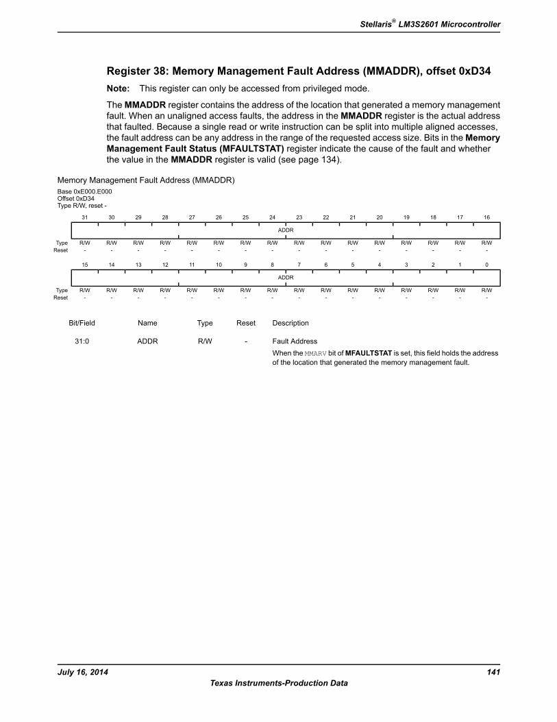
Register 38: Memory Management Fault Address (MMADDR), offset 0xD34Note: This register can only be accessed from privileged mode.
TheMMADDR register contains the address of the location that generated a memory managementfault. When an unaligned access faults, the address in theMMADDR register is the actual addressthat faulted. Because a single read or write instruction can be split into multiple aligned accesses,the fault address can be any address in the range of the requested access size. Bits in theMemoryManagement Fault Status (MFAULTSTAT) register indicate the cause of the fault and whetherthe value in the MMADDR register is valid (see page 134).
Memory Management Fault Address (MMADDR)Base 0xE000.E000Offset 0xD34Type R/W, reset -
16171819202122232425262728293031
ADDR
R/WR/WR/WR/WR/WR/WR/WR/WR/WR/WR/WR/WR/WR/WR/WR/WType----------------Reset
0123456789101112131415
ADDR
R/WR/WR/WR/WR/WR/WR/WR/WR/WR/WR/WR/WR/WR/WR/WR/WType----------------Reset
DescriptionResetTypeNameBit/Field
Fault AddressWhen the MMARV bit ofMFAULTSTAT is set, this field holds the addressof the location that generated the memory management fault.
-R/WADDR31:0
141July 16, 2014Texas Instruments-Production Data
Stellaris® LM3S2601 Microcontroller
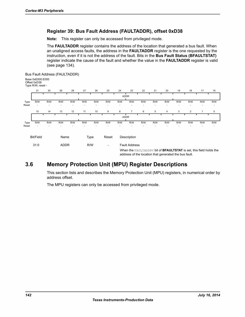
Register 39: Bus Fault Address (FAULTADDR), offset 0xD38Note: This register can only be accessed from privileged mode.
The FAULTADDR register contains the address of the location that generated a bus fault. Whenan unaligned access faults, the address in the FAULTADDR register is the one requested by theinstruction, even if it is not the address of the fault. Bits in the Bus Fault Status (BFAULTSTAT)register indicate the cause of the fault and whether the value in the FAULTADDR register is valid(see page 134).
Bus Fault Address (FAULTADDR)Base 0xE000.E000Offset 0xD38Type R/W, reset -
16171819202122232425262728293031
ADDR
R/WR/WR/WR/WR/WR/WR/WR/WR/WR/WR/WR/WR/WR/WR/WR/WType----------------Reset
0123456789101112131415
ADDR
R/WR/WR/WR/WR/WR/WR/WR/WR/WR/WR/WR/WR/WR/WR/WR/WType----------------Reset
DescriptionResetTypeNameBit/Field
Fault AddressWhen the FAULTADDRV bit of BFAULTSTAT is set, this field holds theaddress of the location that generated the bus fault.
-R/WADDR31:0
3.6 Memory Protection Unit (MPU) Register DescriptionsThis section lists and describes the Memory Protection Unit (MPU) registers, in numerical order byaddress offset.
The MPU registers can only be accessed from privileged mode.
July 16, 2014142Texas Instruments-Production Data
Cortex-M3 Peripherals
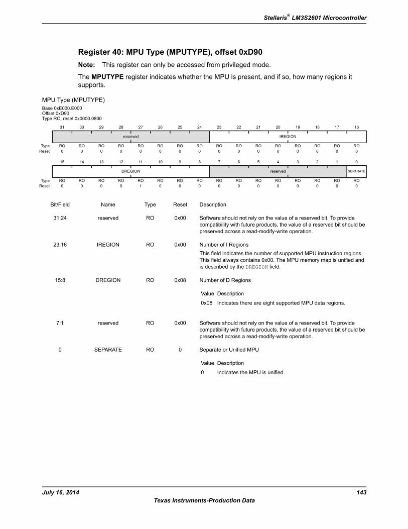
Register 40: MPU Type (MPUTYPE), offset 0xD90Note: This register can only be accessed from privileged mode.
The MPUTYPE register indicates whether the MPU is present, and if so, how many regions itsupports.
MPU Type (MPUTYPE)Base 0xE000.E000Offset 0xD90Type RO, reset 0x0000.0800
16171819202122232425262728293031
IREGIONreserved
ROROROROROROROROROROROROROROROROType0000000000000000Reset
0123456789101112131415
SEPARATEreservedDREGION
ROROROROROROROROROROROROROROROROType0000000000010000Reset
DescriptionResetTypeNameBit/Field
Software should not rely on the value of a reserved bit. To providecompatibility with future products, the value of a reserved bit should bepreserved across a read-modify-write operation.
0x00ROreserved31:24
Number of I RegionsThis field indicates the number of supported MPU instruction regions.This field always contains 0x00. The MPU memory map is unified andis described by the DREGION field.
0x00ROIREGION23:16
Number of D Regions
DescriptionValue
Indicates there are eight supported MPU data regions.0x08
0x08RODREGION15:8
Software should not rely on the value of a reserved bit. To providecompatibility with future products, the value of a reserved bit should bepreserved across a read-modify-write operation.
0x00ROreserved7:1
Separate or Unified MPU
DescriptionValue
Indicates the MPU is unified.0
0ROSEPARATE0
143July 16, 2014Texas Instruments-Production Data
Stellaris® LM3S2601 Microcontroller
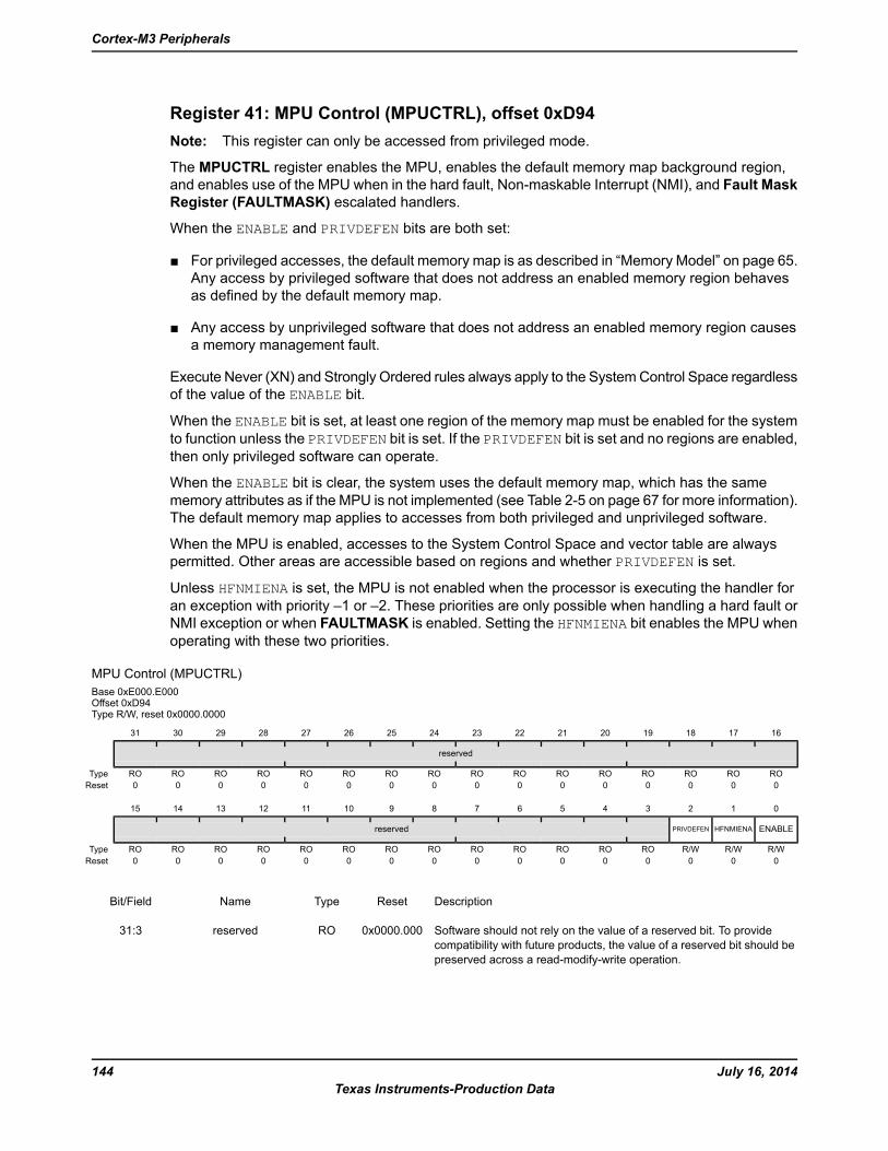
Register 41: MPU Control (MPUCTRL), offset 0xD94Note: This register can only be accessed from privileged mode.
The MPUCTRL register enables the MPU, enables the default memory map background region,and enables use of the MPU when in the hard fault, Non-maskable Interrupt (NMI), and Fault MaskRegister (FAULTMASK) escalated handlers.
When the ENABLE and PRIVDEFEN bits are both set:
For privileged accesses, the default memory map is as described in “Memory Model” on page 65.Any access by privileged software that does not address an enabled memory region behavesas defined by the default memory map.
Any access by unprivileged software that does not address an enabled memory region causesa memory management fault.
Execute Never (XN) and Strongly Ordered rules always apply to the SystemControl Space regardlessof the value of the ENABLE bit.
When the ENABLE bit is set, at least one region of the memory map must be enabled for the systemto function unless the PRIVDEFEN bit is set. If the PRIVDEFEN bit is set and no regions are enabled,then only privileged software can operate.
When the ENABLE bit is clear, the system uses the default memory map, which has the samememory attributes as if the MPU is not implemented (see Table 2-5 on page 67 for more information).The default memory map applies to accesses from both privileged and unprivileged software.
When the MPU is enabled, accesses to the System Control Space and vector table are alwayspermitted. Other areas are accessible based on regions and whether PRIVDEFEN is set.
Unless HFNMIENA is set, the MPU is not enabled when the processor is executing the handler foran exception with priority –1 or –2. These priorities are only possible when handling a hard fault orNMI exception or when FAULTMASK is enabled. Setting the HFNMIENA bit enables the MPU whenoperating with these two priorities.
MPU Control (MPUCTRL)Base 0xE000.E000Offset 0xD94Type R/W, reset 0x0000.0000
16171819202122232425262728293031
reserved
ROROROROROROROROROROROROROROROROType0000000000000000Reset
0123456789101112131415
ENABLEHFNMIENAPRIVDEFENreserved
R/WR/WR/WROROROROROROROROROROROROROType0000000000000000Reset
DescriptionResetTypeNameBit/Field
Software should not rely on the value of a reserved bit. To providecompatibility with future products, the value of a reserved bit should bepreserved across a read-modify-write operation.
0x0000.000ROreserved31:3
July 16, 2014144Texas Instruments-Production Data
Cortex-M3 Peripherals
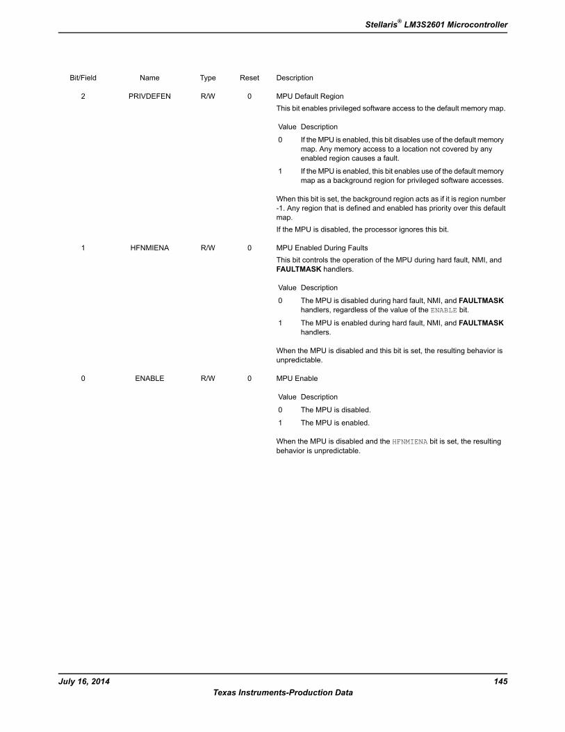
DescriptionResetTypeNameBit/Field
MPU Default RegionThis bit enables privileged software access to the default memory map.
DescriptionValue
If the MPU is enabled, this bit disables use of the default memorymap. Any memory access to a location not covered by anyenabled region causes a fault.
0
If the MPU is enabled, this bit enables use of the default memorymap as a background region for privileged software accesses.
1
When this bit is set, the background region acts as if it is region number-1. Any region that is defined and enabled has priority over this defaultmap.If the MPU is disabled, the processor ignores this bit.
0R/WPRIVDEFEN2
MPU Enabled During FaultsThis bit controls the operation of the MPU during hard fault, NMI, andFAULTMASK handlers.
DescriptionValue
The MPU is disabled during hard fault, NMI, and FAULTMASKhandlers, regardless of the value of the ENABLE bit.
0
The MPU is enabled during hard fault, NMI, and FAULTMASKhandlers.
1
When the MPU is disabled and this bit is set, the resulting behavior isunpredictable.
0R/WHFNMIENA1
MPU Enable
DescriptionValue
The MPU is disabled.0
The MPU is enabled.1
When the MPU is disabled and the HFNMIENA bit is set, the resultingbehavior is unpredictable.
0R/WENABLE0
145July 16, 2014Texas Instruments-Production Data
Stellaris® LM3S2601 Microcontroller
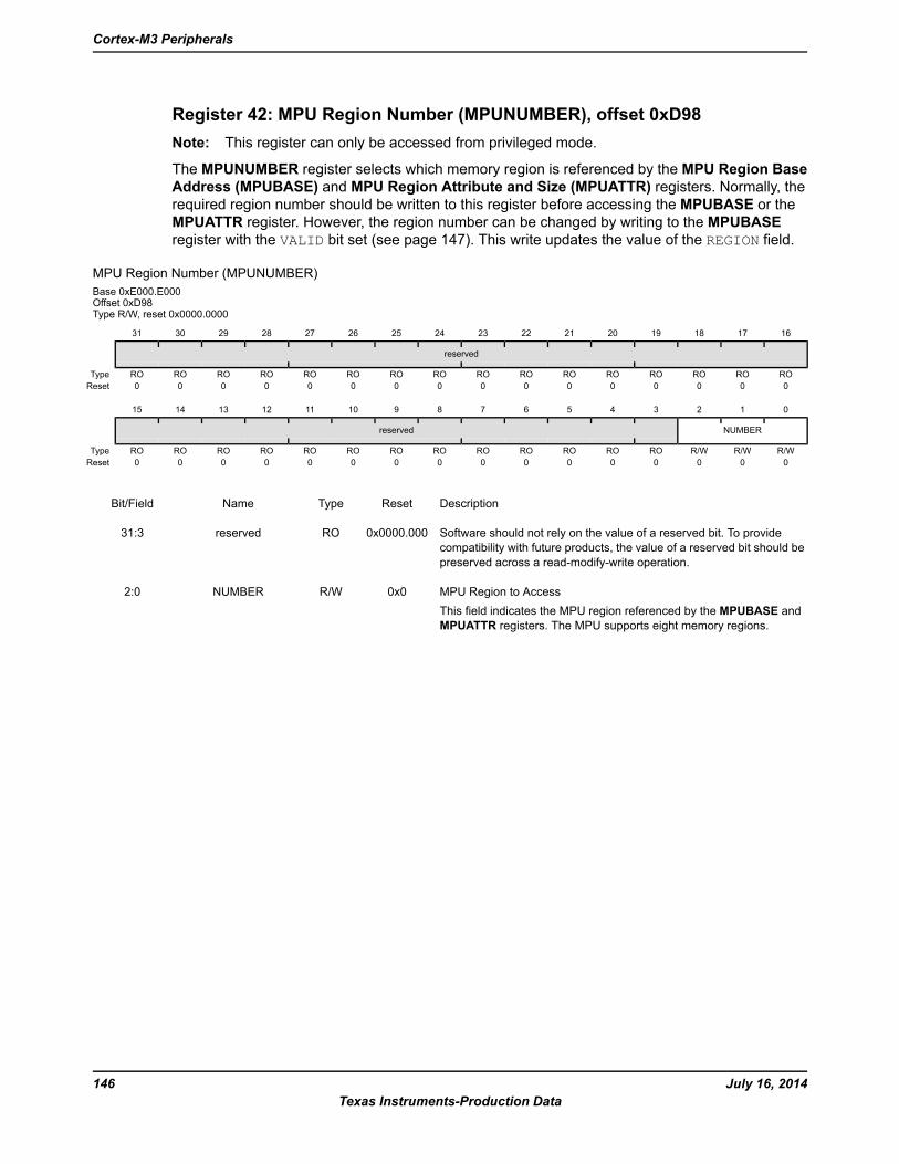
Register 42: MPU Region Number (MPUNUMBER), offset 0xD98Note: This register can only be accessed from privileged mode.
The MPUNUMBER register selects which memory region is referenced by the MPU Region BaseAddress (MPUBASE) and MPU Region Attribute and Size (MPUATTR) registers. Normally, therequired region number should be written to this register before accessing the MPUBASE or theMPUATTR register. However, the region number can be changed by writing to the MPUBASEregister with the VALID bit set (see page 147). This write updates the value of the REGION field.
MPU Region Number (MPUNUMBER)Base 0xE000.E000Offset 0xD98Type R/W, reset 0x0000.0000
16171819202122232425262728293031
reserved
ROROROROROROROROROROROROROROROROType0000000000000000Reset
0123456789101112131415
NUMBERreserved
R/WR/WR/WROROROROROROROROROROROROROType0000000000000000Reset
DescriptionResetTypeNameBit/Field
Software should not rely on the value of a reserved bit. To providecompatibility with future products, the value of a reserved bit should bepreserved across a read-modify-write operation.
0x0000.000ROreserved31:3
MPU Region to AccessThis field indicates the MPU region referenced by the MPUBASE andMPUATTR registers. The MPU supports eight memory regions.
0x0R/WNUMBER2:0
July 16, 2014146Texas Instruments-Production Data
Cortex-M3 Peripherals
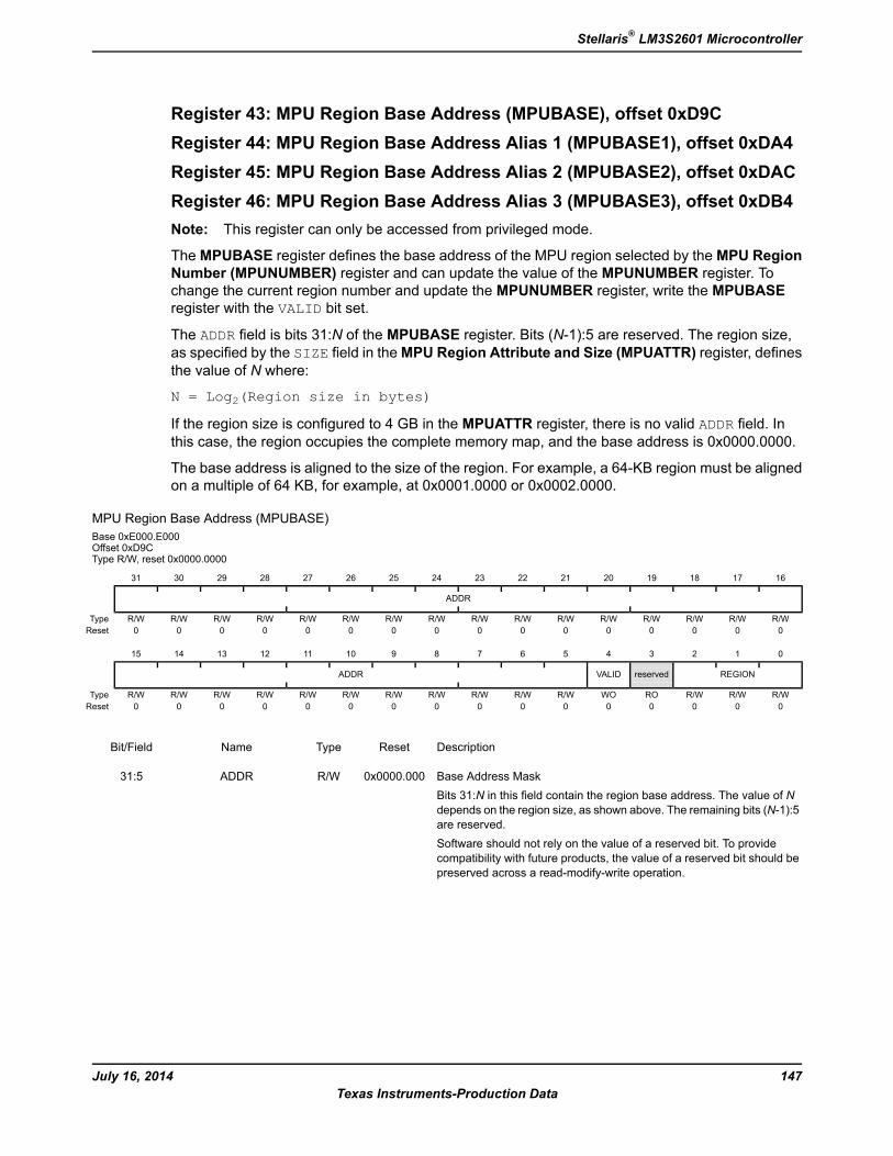
Register 43: MPU Region Base Address (MPUBASE), offset 0xD9CRegister 44: MPU Region Base Address Alias 1 (MPUBASE1), offset 0xDA4Register 45: MPU Region Base Address Alias 2 (MPUBASE2), offset 0xDACRegister 46: MPU Region Base Address Alias 3 (MPUBASE3), offset 0xDB4Note: This register can only be accessed from privileged mode.
The MPUBASE register defines the base address of the MPU region selected by the MPU RegionNumber (MPUNUMBER) register and can update the value of the MPUNUMBER register. Tochange the current region number and update the MPUNUMBER register, write the MPUBASEregister with the VALID bit set.
The ADDR field is bits 31:N of the MPUBASE register. Bits (N-1):5 are reserved. The region size,as specified by the SIZE field in theMPU Region Attribute and Size (MPUATTR) register, definesthe value of N where:
N = Log2(Region size in bytes)
If the region size is configured to 4 GB in the MPUATTR register, there is no valid ADDR field. Inthis case, the region occupies the complete memory map, and the base address is 0x0000.0000.
The base address is aligned to the size of the region. For example, a 64-KB region must be alignedon a multiple of 64 KB, for example, at 0x0001.0000 or 0x0002.0000.
MPU Region Base Address (MPUBASE)Base 0xE000.E000Offset 0xD9CType R/W, reset 0x0000.0000
16171819202122232425262728293031
ADDR
R/WR/WR/WR/WR/WR/WR/WR/WR/WR/WR/WR/WR/WR/WR/WR/WType0000000000000000Reset
0123456789101112131415
REGIONreservedVALIDADDR
R/WR/WR/WROWOR/WR/WR/WR/WR/WR/WR/WR/WR/WR/WR/WType0000000000000000Reset
DescriptionResetTypeNameBit/Field
Base Address MaskBits 31:N in this field contain the region base address. The value of Ndepends on the region size, as shown above. The remaining bits (N-1):5are reserved.Software should not rely on the value of a reserved bit. To providecompatibility with future products, the value of a reserved bit should bepreserved across a read-modify-write operation.
0x0000.000R/WADDR31:5
147July 16, 2014Texas Instruments-Production Data
Stellaris® LM3S2601 Microcontroller
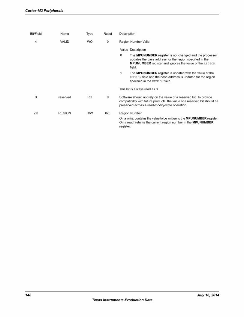
DescriptionResetTypeNameBit/Field
Region Number Valid
DescriptionValue
The MPUNUMBER register is not changed and the processorupdates the base address for the region specified in theMPUNUMBER register and ignores the value of the REGIONfield.
0
The MPUNUMBER register is updated with the value of theREGION field and the base address is updated for the regionspecified in the REGION field.
1
This bit is always read as 0.
0WOVALID4
Software should not rely on the value of a reserved bit. To providecompatibility with future products, the value of a reserved bit should bepreserved across a read-modify-write operation.
0ROreserved3
Region NumberOn a write, contains the value to be written to theMPUNUMBER register.On a read, returns the current region number in the MPUNUMBERregister.
0x0R/WREGION2:0
July 16, 2014148Texas Instruments-Production Data
Cortex-M3 Peripherals
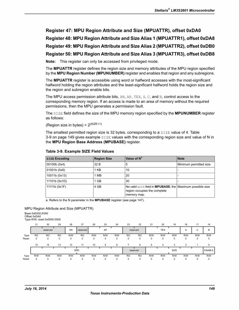
Register 47: MPU Region Attribute and Size (MPUATTR), offset 0xDA0Register 48: MPURegion Attribute and Size Alias 1 (MPUATTR1), offset 0xDA8Register 49: MPURegion Attribute and Size Alias 2 (MPUATTR2), offset 0xDB0Register 50: MPURegion Attribute and Size Alias 3 (MPUATTR3), offset 0xDB8Note: This register can only be accessed from privileged mode.
The MPUATTR register defines the region size and memory attributes of the MPU region specifiedby theMPURegion Number (MPUNUMBER) register and enables that region and any subregions.
The MPUATTR register is accessible using word or halfword accesses with the most-significanthalfword holding the region attributes and the least-significant halfword holds the region size andthe region and subregion enable bits.
The MPU access permission attribute bits, XN, AP, TEX, S, C, and B, control access to thecorresponding memory region. If an access is made to an area of memory without the requiredpermissions, then the MPU generates a permission fault.
The SIZE field defines the size of the MPU memory region specified by theMPUNUMBER registeras follows:
(Region size in bytes) = 2(SIZE+1)
The smallest permitted region size is 32 bytes, corresponding to a SIZE value of 4. Table3-9 on page 149 gives example SIZE values with the corresponding region size and value of N inthe MPU Region Base Address (MPUBASE) register.
Table 3-9. Example SIZE Field Values
NoteValue of NaRegion SizeSIZE Encoding
Minimum permitted size532 B00100b (0x4)
-101 KB01001b (0x9)
-201 MB10011b (0x13)
-301 GB11101b (0x1D)
Maximum possible sizeNo valid ADDR field inMPUBASE; theregion occupies the completememory map.
4 GB11111b (0x1F)
a. Refers to the N parameter in the MPUBASE register (see page 147).
MPU Region Attribute and Size (MPUATTR)Base 0xE000.E000Offset 0xDA0Type R/W, reset 0x0000.0000
16171819202122232425262728293031
BCSTEXreservedAPreservedXNreserved
R/WR/WR/WR/WR/WR/WROROR/WR/WR/WROR/WROROROType0000000000000000Reset
0123456789101112131415
ENABLESIZEreservedSRD
R/WR/WR/WR/WR/WR/WROROR/WR/WR/WR/WR/WR/WR/WR/WType0000000000000000Reset
149July 16, 2014Texas Instruments-Production Data
Stellaris® LM3S2601 Microcontroller
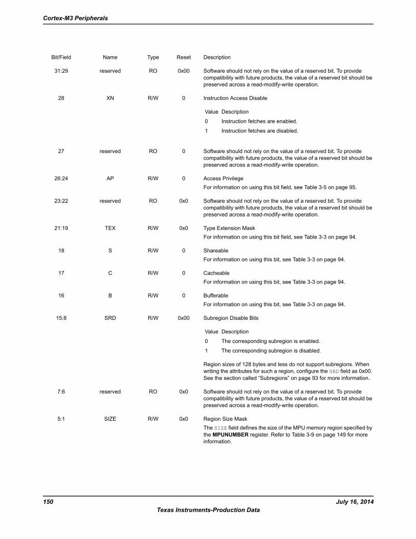
DescriptionResetTypeNameBit/Field
Software should not rely on the value of a reserved bit. To providecompatibility with future products, the value of a reserved bit should bepreserved across a read-modify-write operation.
0x00ROreserved31:29
Instruction Access Disable
DescriptionValue
Instruction fetches are enabled.0
Instruction fetches are disabled.1
0R/WXN28
Software should not rely on the value of a reserved bit. To providecompatibility with future products, the value of a reserved bit should bepreserved across a read-modify-write operation.
0ROreserved27
Access PrivilegeFor information on using this bit field, see Table 3-5 on page 95.
0R/WAP26:24
Software should not rely on the value of a reserved bit. To providecompatibility with future products, the value of a reserved bit should bepreserved across a read-modify-write operation.
0x0ROreserved23:22
Type Extension MaskFor information on using this bit field, see Table 3-3 on page 94.
0x0R/WTEX21:19
ShareableFor information on using this bit, see Table 3-3 on page 94.
0R/WS18
CacheableFor information on using this bit, see Table 3-3 on page 94.
0R/WC17
BufferableFor information on using this bit, see Table 3-3 on page 94.
0R/WB16
Subregion Disable Bits
DescriptionValue
The corresponding subregion is enabled.0
The corresponding subregion is disabled.1
Region sizes of 128 bytes and less do not support subregions. Whenwriting the attributes for such a region, configure the SRD field as 0x00.See the section called “Subregions” on page 93 for more information.
0x00R/WSRD15:8
Software should not rely on the value of a reserved bit. To providecompatibility with future products, the value of a reserved bit should bepreserved across a read-modify-write operation.
0x0ROreserved7:6
Region Size MaskThe SIZE field defines the size of the MPU memory region specified bythe MPUNUMBER register. Refer to Table 3-9 on page 149 for moreinformation.
0x0R/WSIZE5:1
July 16, 2014150Texas Instruments-Production Data
Cortex-M3 Peripherals

DescriptionResetTypeNameBit/Field
Region Enable
DescriptionValue
The region is disabled.0
The region is enabled.1
0R/WENABLE0
151July 16, 2014Texas Instruments-Production Data
Stellaris® LM3S2601 Microcontroller
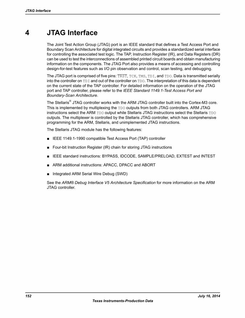
4 JTAG InterfaceThe Joint Test Action Group (JTAG) port is an IEEE standard that defines a Test Access Port andBoundary Scan Architecture for digital integrated circuits and provides a standardized serial interfacefor controlling the associated test logic. The TAP, Instruction Register (IR), and Data Registers (DR)can be used to test the interconnections of assembled printed circuit boards and obtain manufacturinginformation on the components. The JTAG Port also provides a means of accessing and controllingdesign-for-test features such as I/O pin observation and control, scan testing, and debugging.
The JTAG port is comprised of five pins: TRST, TCK, TMS, TDI, and TDO. Data is transmitted seriallyinto the controller on TDI and out of the controller on TDO. The interpretation of this data is dependenton the current state of the TAP controller. For detailed information on the operation of the JTAGport and TAP controller, please refer to the IEEE Standard 1149.1-Test Access Port andBoundary-Scan Architecture.
The Stellaris® JTAG controller works with the ARM JTAG controller built into the Cortex-M3 core.This is implemented by multiplexing the TDO outputs from both JTAG controllers. ARM JTAGinstructions select the ARM TDO output while Stellaris JTAG instructions select the Stellaris TDOoutputs. The multiplexer is controlled by the Stellaris JTAG controller, which has comprehensiveprogramming for the ARM, Stellaris, and unimplemented JTAG instructions.
The Stellaris JTAG module has the following features:
IEEE 1149.1-1990 compatible Test Access Port (TAP) controller
Four-bit Instruction Register (IR) chain for storing JTAG instructions
IEEE standard instructions: BYPASS, IDCODE, SAMPLE/PRELOAD, EXTEST and INTEST
ARM additional instructions: APACC, DPACC and ABORT
Integrated ARM Serial Wire Debug (SWD)
See the ARM® Debug Interface V5 Architecture Specification for more information on the ARMJTAG controller.
July 16, 2014152Texas Instruments-Production Data
JTAG Interface
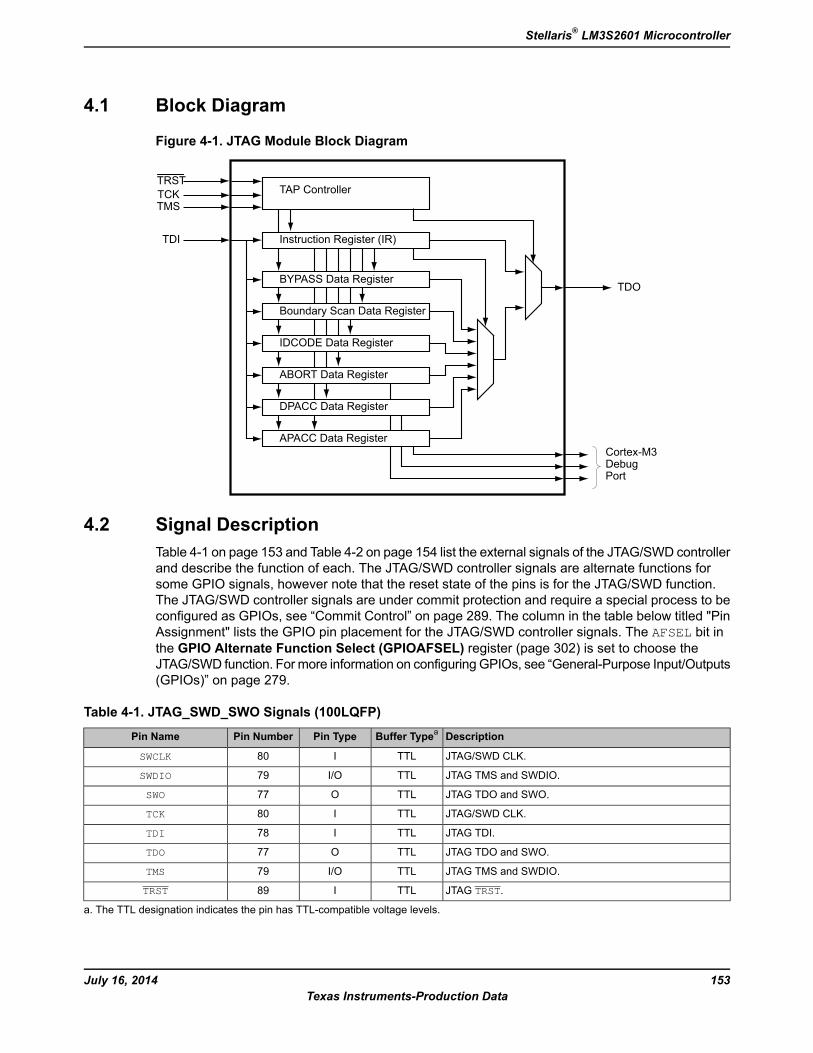
4.1 Block Diagram
Figure 4-1. JTAG Module Block Diagram
Instruction Register (IR)
TAP Controller
BYPASS Data Register
Boundary Scan Data Register
IDCODE Data Register
ABORT Data Register
DPACC Data Register
APACC Data Register
TCKTMS
TDI
TDO
Cortex-M3DebugPort
TRST
4.2 Signal DescriptionTable 4-1 on page 153 and Table 4-2 on page 154 list the external signals of the JTAG/SWD controllerand describe the function of each. The JTAG/SWD controller signals are alternate functions forsome GPIO signals, however note that the reset state of the pins is for the JTAG/SWD function.The JTAG/SWD controller signals are under commit protection and require a special process to beconfigured as GPIOs, see “Commit Control” on page 289. The column in the table below titled "PinAssignment" lists the GPIO pin placement for the JTAG/SWD controller signals. The AFSEL bit inthe GPIO Alternate Function Select (GPIOAFSEL) register (page 302) is set to choose theJTAG/SWD function. For more information on configuringGPIOs, see “General-Purpose Input/Outputs(GPIOs)” on page 279.
Table 4-1. JTAG_SWD_SWO Signals (100LQFP)
DescriptionBuffer TypeaPin TypePin NumberPin Name
JTAG/SWD CLK.TTLI80SWCLK
JTAG TMS and SWDIO.TTLI/O79SWDIO
JTAG TDO and SWO.TTLO77SWO
JTAG/SWD CLK.TTLI80TCK
JTAG TDI.TTLI78TDI
JTAG TDO and SWO.TTLO77TDO
JTAG TMS and SWDIO.TTLI/O79TMS
JTAG TRST.TTLI89TRST
a. The TTL designation indicates the pin has TTL-compatible voltage levels.
153July 16, 2014Texas Instruments-Production Data
Stellaris® LM3S2601 Microcontroller
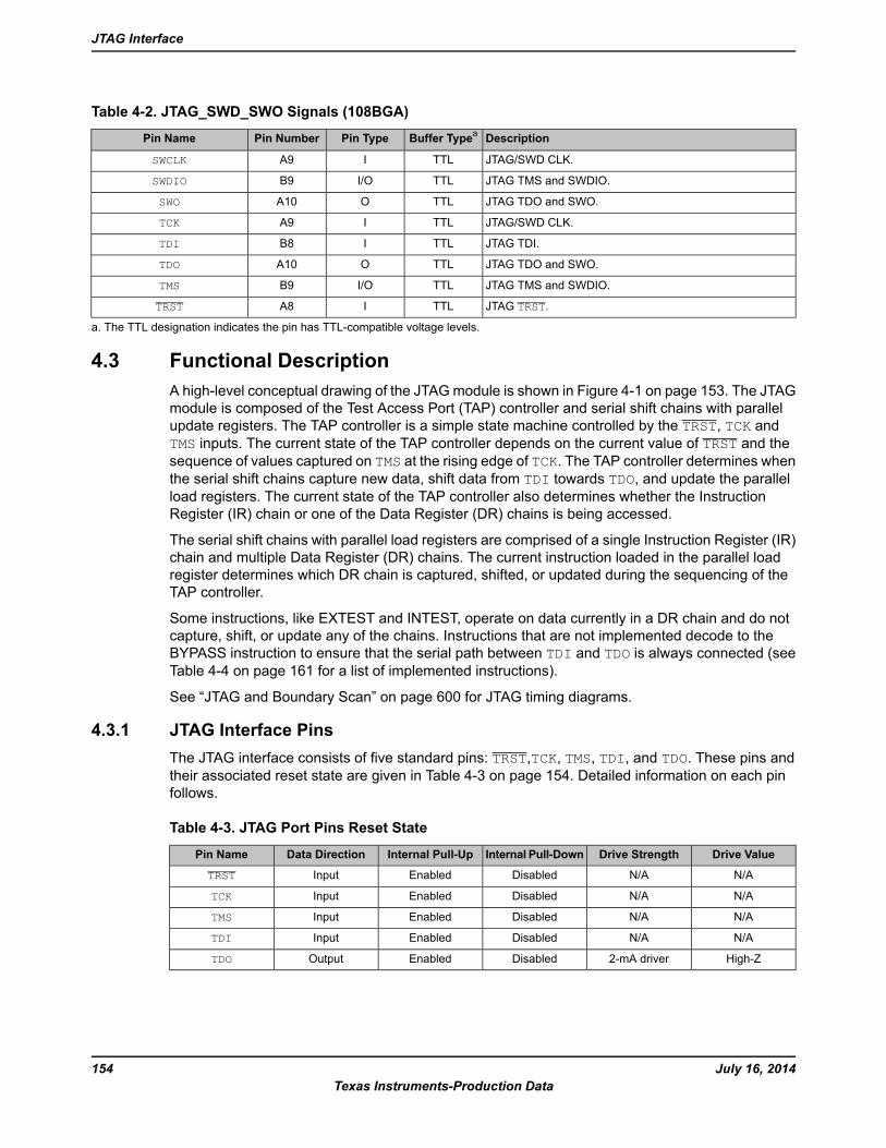
Table 4-2. JTAG_SWD_SWO Signals (108BGA)
DescriptionBuffer TypeaPin TypePin NumberPin Name
JTAG/SWD CLK.TTLIA9SWCLK
JTAG TMS and SWDIO.TTLI/OB9SWDIO
JTAG TDO and SWO.TTLOA10SWO
JTAG/SWD CLK.TTLIA9TCK
JTAG TDI.TTLIB8TDI
JTAG TDO and SWO.TTLOA10TDO
JTAG TMS and SWDIO.TTLI/OB9TMS
JTAG TRST.TTLIA8TRST
a. The TTL designation indicates the pin has TTL-compatible voltage levels.
4.3 Functional DescriptionA high-level conceptual drawing of the JTAGmodule is shown in Figure 4-1 on page 153. The JTAGmodule is composed of the Test Access Port (TAP) controller and serial shift chains with parallelupdate registers. The TAP controller is a simple state machine controlled by the TRST, TCK andTMS inputs. The current state of the TAP controller depends on the current value of TRST and thesequence of values captured on TMS at the rising edge of TCK. The TAP controller determines whenthe serial shift chains capture new data, shift data from TDI towards TDO, and update the parallelload registers. The current state of the TAP controller also determines whether the InstructionRegister (IR) chain or one of the Data Register (DR) chains is being accessed.
The serial shift chains with parallel load registers are comprised of a single Instruction Register (IR)chain and multiple Data Register (DR) chains. The current instruction loaded in the parallel loadregister determines which DR chain is captured, shifted, or updated during the sequencing of theTAP controller.
Some instructions, like EXTEST and INTEST, operate on data currently in a DR chain and do notcapture, shift, or update any of the chains. Instructions that are not implemented decode to theBYPASS instruction to ensure that the serial path between TDI and TDO is always connected (seeTable 4-4 on page 161 for a list of implemented instructions).
See “JTAG and Boundary Scan” on page 600 for JTAG timing diagrams.
4.3.1 JTAG Interface PinsThe JTAG interface consists of five standard pins: TRST,TCK, TMS, TDI, and TDO. These pins andtheir associated reset state are given in Table 4-3 on page 154. Detailed information on each pinfollows.
Table 4-3. JTAG Port Pins Reset State
Drive ValueDrive StrengthInternal Pull-DownInternal Pull-UpData DirectionPin Name
N/AN/ADisabledEnabledInputTRST
N/AN/ADisabledEnabledInputTCK
N/AN/ADisabledEnabledInputTMS
N/AN/ADisabledEnabledInputTDI
High-Z2-mA driverDisabledEnabledOutputTDO
July 16, 2014154Texas Instruments-Production Data
JTAG Interface
4.3.1.1 Test Reset Input (TRST)The TRST pin is an asynchronous active Low input signal for initializing and resetting the JTAG TAPcontroller and associated JTAG circuitry. When TRST is asserted, the TAP controller resets to theTest-Logic-Reset state and remains there while TRST is asserted. When the TAP controller entersthe Test-Logic-Reset state, the JTAG Instruction Register (IR) resets to the default instruction,IDCODE.
By default, the internal pull-up resistor on the TRST pin is enabled after reset. Changes to the pull-upresistor settings on GPIO Port B should ensure that the internal pull-up resistor remains enabledon PB7/TRST; otherwise JTAG communication could be lost.
4.3.1.2 Test Clock Input (TCK)The TCK pin is the clock for the JTAG module. This clock is provided so the test logic can operateindependently of any other system clocks. In addition, it ensures that multiple JTAG TAP controllersthat are daisy-chained together can synchronously communicate serial test data betweencomponents. During normal operation, TCK is driven by a free-running clock with a nominal 50%duty cycle. When necessary, TCK can be stopped at 0 or 1 for extended periods of time. While TCKis stopped at 0 or 1, the state of the TAP controller does not change and data in the JTAG Instructionand Data Registers is not lost.
By default, the internal pull-up resistor on the TCK pin is enabled after reset. This assures that noclocking occurs if the pin is not driven from an external source. The internal pull-up and pull-downresistors can be turned off to save internal power as long as the TCK pin is constantly being drivenby an external source.
4.3.1.3 Test Mode Select (TMS)The TMS pin selects the next state of the JTAG TAP controller. TMS is sampled on the rising edgeof TCK. Depending on the current TAP state and the sampled value of TMS, the next state is entered.Because the TMS pin is sampled on the rising edge of TCK, the IEEE Standard 1149.1 expects thevalue on TMS to change on the falling edge of TCK.
Holding TMS high for five consecutive TCK cycles drives the TAP controller state machine to theTest-Logic-Reset state. When the TAP controller enters the Test-Logic-Reset state, the JTAGInstruction Register (IR) resets to the default instruction, IDCODE. Therefore, this sequence canbe used as a reset mechanism, similar to asserting TRST. The JTAG Test Access Port state machinecan be seen in its entirety in Figure 4-2 on page 157.
By default, the internal pull-up resistor on the TMS pin is enabled after reset. Changes to the pull-upresistor settings on GPIO Port C should ensure that the internal pull-up resistor remains enabledon PC1/TMS; otherwise JTAG communication could be lost.
4.3.1.4 Test Data Input (TDI)The TDI pin provides a stream of serial information to the IR chain and the DR chains. TDI issampled on the rising edge of TCK and, depending on the current TAP state and the currentinstruction, presents this data to the proper shift register chain. Because the TDI pin is sampled onthe rising edge of TCK, the IEEE Standard 1149.1 expects the value on TDI to change on the fallingedge of TCK.
By default, the internal pull-up resistor on the TDI pin is enabled after reset. Changes to the pull-upresistor settings on GPIO Port C should ensure that the internal pull-up resistor remains enabledon PC2/TDI; otherwise JTAG communication could be lost.
155July 16, 2014Texas Instruments-Production Data
Stellaris® LM3S2601 Microcontroller
4.3.1.5 Test Data Output (TDO)The TDO pin provides an output stream of serial information from the IR chain or the DR chains.The value of TDO depends on the current TAP state, the current instruction, and the data in thechain being accessed. In order to save power when the JTAG port is not being used, the TDO pinis placed in an inactive drive state when not actively shifting out data. Because TDO can be connectedto the TDI of another controller in a daisy-chain configuration, the IEEE Standard 1149.1 expectsthe value on TDO to change on the falling edge of TCK.
By default, the internal pull-up resistor on the TDO pin is enabled after reset. This assures that thepin remains at a constant logic level when the JTAG port is not being used. The internal pull-up andpull-down resistors can be turned off to save internal power if a High-Z output value is acceptableduring certain TAP controller states.
4.3.2 JTAG TAP ControllerThe JTAG TAP controller state machine is shown in Figure 4-2 on page 157. The TAP controllerstate machine is reset to the Test-Logic-Reset state on the assertion of a Power-On-Reset (POR)or the assertion of TRST. Asserting the correct sequence on the TMS pin allows the JTAG moduleto shift in new instructions, shift in data, or idle during extended testing sequences. For detailedinformation on the function of the TAP controller and the operations that occur in each state, pleaserefer to IEEE Standard 1149.1.
July 16, 2014156Texas Instruments-Production Data
JTAG Interface
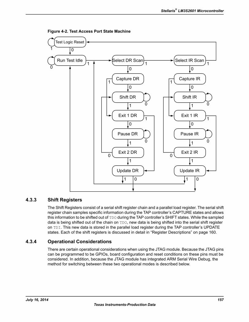
Figure 4-2. Test Access Port State Machine
Test Logic Reset
Run Test Idle Select DR Scan Select IR Scan
Capture DR Capture IR
Shift DR Shift IR
Exit 1 DR Exit 1 IR
Exit 2 DR Exit 2 IR
Pause DR Pause IR
Update DR Update IR
1 11
1 1
1
1 1
1 1
1 1
1 1
1 10 0
00
00
0 0
0 0
0 0
00
0
0
4.3.3 Shift RegistersThe Shift Registers consist of a serial shift register chain and a parallel load register. The serial shiftregister chain samples specific information during the TAP controller’s CAPTURE states and allowsthis information to be shifted out of TDO during the TAP controller’s SHIFT states. While the sampleddata is being shifted out of the chain on TDO, new data is being shifted into the serial shift registeron TDI. This new data is stored in the parallel load register during the TAP controller’s UPDATEstates. Each of the shift registers is discussed in detail in “Register Descriptions” on page 160.
4.3.4 Operational ConsiderationsThere are certain operational considerations when using the JTAGmodule. Because the JTAG pinscan be programmed to be GPIOs, board configuration and reset conditions on these pins must beconsidered. In addition, because the JTAG module has integrated ARM Serial Wire Debug, themethod for switching between these two operational modes is described below.
157July 16, 2014Texas Instruments-Production Data
Stellaris® LM3S2601 Microcontroller
4.3.4.1 GPIO FunctionalityWhen the controller is reset with either a POR or RST, the JTAG/SWD port pins default to theirJTAG/SWD configurations. The default configuration includes enabling digital functionality (settingGPIODEN to 1), enabling the pull-up resistors (setting GPIOPUR to 1), and enabling the alternatehardware function (setting GPIOAFSEL to 1) for the PB7 and PC[3:0] JTAG/SWD pins.
It is possible for software to configure these pins as GPIOs after reset by writing 0s to PB7 andPC[3:0] in theGPIOAFSEL register. If the user does not require the JTAG/SWD port for debuggingor board-level testing, this provides five more GPIOs for use in the design.
Caution – It is possible to create a software sequence that prevents the debugger from connecting tothe Stellaris microcontroller. If the program code loaded into flash immediately changes the JTAG pinsto their GPIO functionality, the debugger may not have enough time to connect and halt the controllerbefore the JTAG pin functionality switches. This may lock the debugger out of the part. This can beavoided with a software routine that restores JTAG functionality based on an external or softwaretrigger.
The GPIO commit control registers provide a layer of protection against accidental programming ofcritical hardware peripherals. Protection is currently provided for the five JTAG/SWD pins (PB7 andPC[3:0]). Writes to protected bits of the GPIO Alternate Function Select (GPIOAFSEL) register(see page 302) are not committed to storage unless the GPIO Lock (GPIOLOCK) register (seepage 312) has been unlocked and the appropriate bits of theGPIO Commit (GPIOCR) register (seepage 313) have been set to 1.
Recovering a "Locked" Device
Note: The mass erase of the flash memory caused by the below sequence erases the entire flashmemory, regardless of the settings in the Flash Memory Protection Program Enable n(FMPPEn) registers. Performing the sequence below does not affect the nonvolatile registersdiscussed in “Nonvolatile Register Programming” on page 256.
If software configures any of the JTAG/SWD pins as GPIO and loses the ability to communicatewith the debugger, there is a debug sequence that can be used to recover the device. Performinga total of ten JTAG-to-SWD and SWD-to-JTAG switch sequences while holding the device in resetmass erases the flash memory. The sequence to recover the device is:
1. Assert and hold the RST signal.
2. Apply power to the device.
3. Perform the JTAG-to-SWD switch sequence.
4. Perform the SWD-to-JTAG switch sequence.
5. Perform the JTAG-to-SWD switch sequence.
6. Perform the SWD-to-JTAG switch sequence.
7. Perform the JTAG-to-SWD switch sequence.
8. Perform the SWD-to-JTAG switch sequence.
9. Perform the JTAG-to-SWD switch sequence.
10. Perform the SWD-to-JTAG switch sequence.
July 16, 2014158Texas Instruments-Production Data
JTAG Interface
11. Perform the JTAG-to-SWD switch sequence.
12. Perform the SWD-to-JTAG switch sequence.
13. Release the RST signal.
14. Wait 400 ms.
15. Power-cycle the device.
The JTAG-to-SWD and SWD-to-JTAG switch sequences are described in “ARM Serial Wire Debug(SWD)” on page 159. When performing switch sequences for the purpose of recovering the debugcapabilities of the device, only steps 1 and 2 of the switch sequence in the section called“JTAG-to-SWD Switching” on page 159 must be performed.
4.3.4.2 Communication with JTAG/SWDBecause the debug clock and the system clock can be running at different frequencies, care mustbe taken to maintain reliable communication with the JTAG/SWD interface. In the Capture-DR state,the result of the previous transaction, if any, is returned, together with a 3-bit ACK response. Softwareshould check the ACK response to see if the previous operation has completed before initiating anew transaction. Alternatively, if the system clock is at least 8 times faster than the debug clock(TCK or SWCLK), the previous operation has enough time to complete and the ACK bits do not haveto be checked.
4.3.4.3 ARM Serial Wire Debug (SWD)In order to seamlessly integrate the ARM Serial Wire Debug (SWD) functionality, a serial-wiredebugger must be able to connect to the Cortex-M3 core without having to perform, or have anyknowledge of, JTAG cycles. This is accomplished with a SWD preamble that is issued before theSWD session begins.
The switching preamble used to enable the SWD interface of the SWJ-DP module starts with theTAP controller in the Test-Logic-Reset state. From here, the preamble sequences the TAP controllerthrough the following states: Run Test Idle, Select DR, Select IR, Test Logic Reset, Test LogicReset, Run Test Idle, Run Test Idle, Select DR, Select IR, Test Logic Reset, Test Logic Reset, RunTest Idle, Run Test Idle, Select DR, Select IR, and Test Logic Reset states.
Stepping through this sequences of the TAP state machine enables the SWD interface and disablesthe JTAG interface. For more information on this operation and the SWD interface, see the ARM®Debug Interface V5 Architecture Specification.
Because this sequence is a valid series of JTAG operations that could be issued, the ARM JTAGTAP controller is not fully compliant to the IEEE Standard 1149.1. This is the only instance wherethe ARM JTAG TAP controller does not meet full compliance with the specification. Due to the lowprobability of this sequence occurring during normal operation of the TAP controller, it should notaffect normal performance of the JTAG interface.
JTAG-to-SWD Switching
To switch the operating mode of the Debug Access Port (DAP) from JTAG to SWD mode, theexternal debug hardware must send the switching preamble to the microcontroller. The 16-bitTMS/SWDIO command for switching to SWDmode is defined as b1110.0111.1001.1110, transmittedLSB first. This command can also be represented as 0xE79E when transmitted LSB first. Thecomplete switch sequence should consist of the following transactions on the TCK/SWCLK andTMS/SWDIO signals:
159July 16, 2014Texas Instruments-Production Data
Stellaris® LM3S2601 Microcontroller
1. Send at least 50 TCK/SWCLK cycles with TMS/SWDIO High to ensure that both JTAG and SWDare in their reset states.
2. Send the 16-bit JTAG-to-SWD switch command, 0xE79E, on TMS/SWDIO.
3. Send at least 50 TCK/SWCLK cycles with TMS/SWDIO High to ensure that if SWJ-DP was alreadyin SWD mode before sending the switch sequence, the SWD goes into the line reset state.
To verify that the Debug Access Port (DAP) has switched to the Serial Wire Debug (SWD) operatingmode, perform a SWD READID operation. The ID value can be compared against the device'sknown ID to verify the switch.
SWD-to-JTAG Switching
To switch the operating mode of the Debug Access Port (DAP) from SWD to JTAG mode, theexternal debug hardware must send a switch command to themicrocontroller. The 16-bit TMS/SWDIOcommand for switching to JTAG mode is defined as b1110.0111.0011.1100, transmitted LSB first.This command can also be represented as 0xE73C when transmitted LSB first. The complete switchsequence should consist of the following transactions on the TCK/SWCLK and TMS/SWDIO signals:
1. Send at least 50 TCK/SWCLK cycles with TMS/SWDIO High to ensure that both JTAG and SWDare in their reset states.
2. Send the 16-bit SWD-to-JTAG switch command, 0xE73C, on TMS/SWDIO.
3. Send at least 50 TCK/SWCLK cycles with TMS/SWDIO High to ensure that if SWJ-DP was alreadyin JTAG mode before sending the switch sequence, the JTAG goes into the Test Logic Resetstate.
To verify that the Debug Access Port (DAP) has switched to the JTAG operating mode, set theJTAG Instruction Register (IR) to the IDCODE instruction and shift out the Data Register (DR). TheDR value can be compared against the device's known IDCODE to verify the switch.
4.4 Initialization and ConfigurationAfter a Power-On-Reset or an external reset (RST), the JTAG pins are automatically configured forJTAG communication. No user-defined initialization or configuration is needed. However, if the userapplication changes these pins to their GPIO function, they must be configured back to their JTAGfunctionality before JTAG communication can be restored. This is done by enabling the five JTAGpins (PB7 and PC[3:0]) for their alternate function using the GPIOAFSEL register. In addition toenabling the alternate functions, any other changes to the GPIO pad configurations on the five JTAGpins (PB7 andPC[3:0]) should be reverted to their default settings.
4.5 Register DescriptionsThere are no APB-accessible registers in the JTAG TAP Controller or Shift Register chains. Theregisters within the JTAG controller are all accessed serially through the TAP Controller. The registerscan be broken down into two main categories: Instruction Registers and Data Registers.
4.5.1 Instruction Register (IR)The JTAG TAP Instruction Register (IR) is a four-bit serial scan chain connected between the JTAGTDI and TDO pins with a parallel load register. When the TAP Controller is placed in the correctstates, bits can be shifted into the Instruction Register. Once these bits have been shifted into thechain and updated, they are interpreted as the current instruction. The decode of the Instruction
July 16, 2014160Texas Instruments-Production Data
JTAG Interface
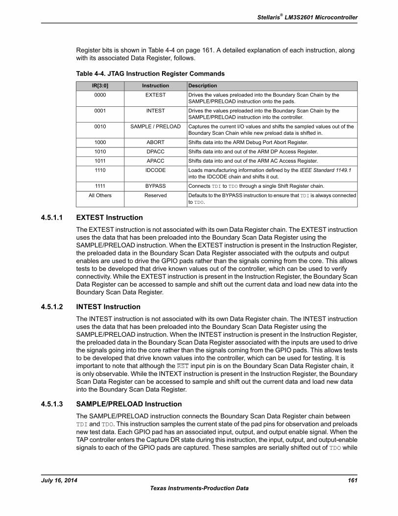
Register bits is shown in Table 4-4 on page 161. A detailed explanation of each instruction, alongwith its associated Data Register, follows.
Table 4-4. JTAG Instruction Register Commands
DescriptionInstructionIR[3:0]
Drives the values preloaded into the Boundary Scan Chain by theSAMPLE/PRELOAD instruction onto the pads.
EXTEST0000
Drives the values preloaded into the Boundary Scan Chain by theSAMPLE/PRELOAD instruction into the controller.
INTEST0001
Captures the current I/O values and shifts the sampled values out of theBoundary Scan Chain while new preload data is shifted in.
SAMPLE / PRELOAD0010
Shifts data into the ARM Debug Port Abort Register.ABORT1000
Shifts data into and out of the ARM DP Access Register.DPACC1010
Shifts data into and out of the ARM AC Access Register.APACC1011
Loads manufacturing information defined by the IEEE Standard 1149.1into the IDCODE chain and shifts it out.
IDCODE1110
Connects TDI to TDO through a single Shift Register chain.BYPASS1111
Defaults to the BYPASS instruction to ensure that TDI is always connectedto TDO.
ReservedAll Others
4.5.1.1 EXTEST InstructionThe EXTEST instruction is not associated with its own Data Register chain. The EXTEST instructionuses the data that has been preloaded into the Boundary Scan Data Register using theSAMPLE/PRELOAD instruction. When the EXTEST instruction is present in the Instruction Register,the preloaded data in the Boundary Scan Data Register associated with the outputs and outputenables are used to drive the GPIO pads rather than the signals coming from the core. This allowstests to be developed that drive known values out of the controller, which can be used to verifyconnectivity. While the EXTEST instruction is present in the Instruction Register, the Boundary ScanData Register can be accessed to sample and shift out the current data and load new data into theBoundary Scan Data Register.
4.5.1.2 INTEST InstructionThe INTEST instruction is not associated with its own Data Register chain. The INTEST instructionuses the data that has been preloaded into the Boundary Scan Data Register using theSAMPLE/PRELOAD instruction. When the INTEST instruction is present in the Instruction Register,the preloaded data in the Boundary Scan Data Register associated with the inputs are used to drivethe signals going into the core rather than the signals coming from the GPIO pads. This allows teststo be developed that drive known values into the controller, which can be used for testing. It isimportant to note that although the RST input pin is on the Boundary Scan Data Register chain, itis only observable. While the INTEXT instruction is present in the Instruction Register, the BoundaryScan Data Register can be accessed to sample and shift out the current data and load new datainto the Boundary Scan Data Register.
4.5.1.3 SAMPLE/PRELOAD InstructionThe SAMPLE/PRELOAD instruction connects the Boundary Scan Data Register chain betweenTDI and TDO. This instruction samples the current state of the pad pins for observation and preloadsnew test data. Each GPIO pad has an associated input, output, and output enable signal. When theTAP controller enters the Capture DR state during this instruction, the input, output, and output-enablesignals to each of the GPIO pads are captured. These samples are serially shifted out of TDO while
161July 16, 2014Texas Instruments-Production Data
Stellaris® LM3S2601 Microcontroller
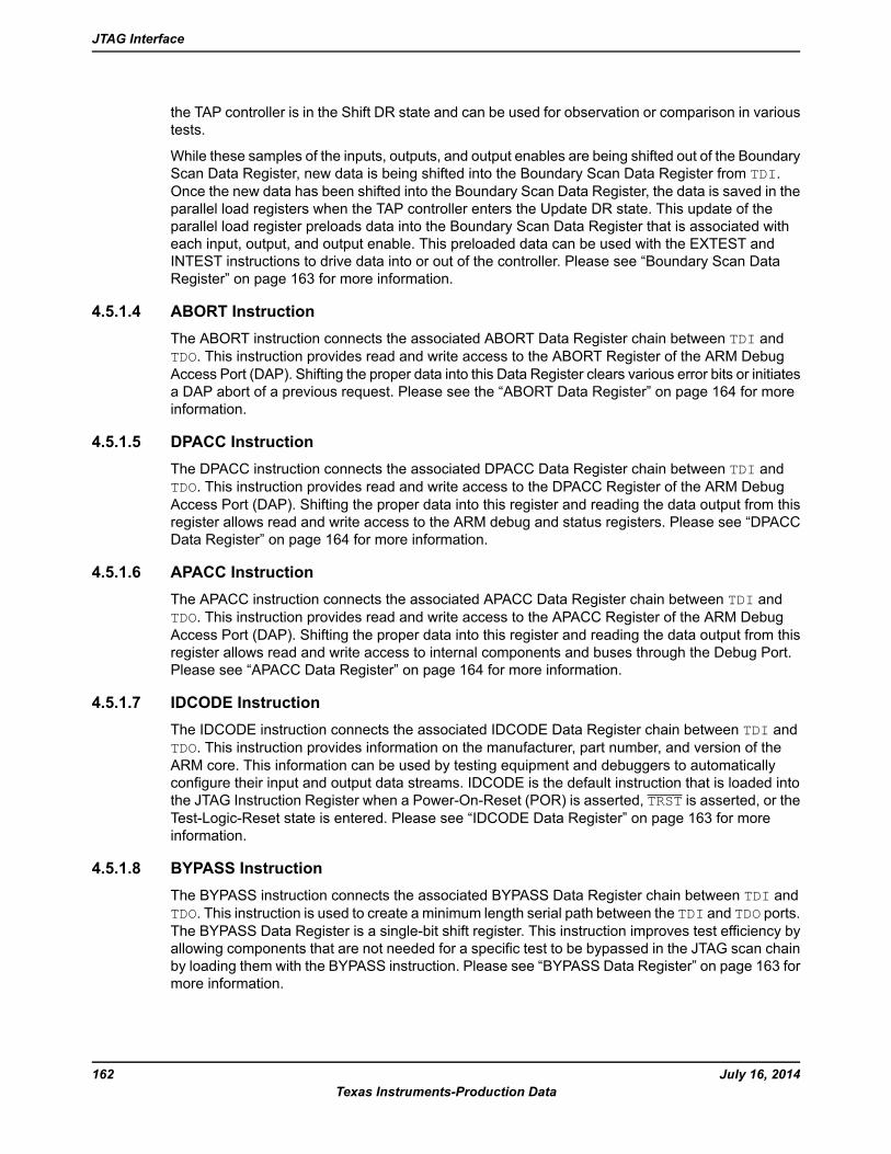
the TAP controller is in the Shift DR state and can be used for observation or comparison in varioustests.
While these samples of the inputs, outputs, and output enables are being shifted out of the BoundaryScan Data Register, new data is being shifted into the Boundary Scan Data Register from TDI.Once the new data has been shifted into the Boundary Scan Data Register, the data is saved in theparallel load registers when the TAP controller enters the Update DR state. This update of theparallel load register preloads data into the Boundary Scan Data Register that is associated witheach input, output, and output enable. This preloaded data can be used with the EXTEST andINTEST instructions to drive data into or out of the controller. Please see “Boundary Scan DataRegister” on page 163 for more information.
4.5.1.4 ABORT InstructionThe ABORT instruction connects the associated ABORT Data Register chain between TDI andTDO. This instruction provides read and write access to the ABORT Register of the ARM DebugAccess Port (DAP). Shifting the proper data into this Data Register clears various error bits or initiatesa DAP abort of a previous request. Please see the “ABORT Data Register” on page 164 for moreinformation.
4.5.1.5 DPACC InstructionThe DPACC instruction connects the associated DPACC Data Register chain between TDI andTDO. This instruction provides read and write access to the DPACC Register of the ARM DebugAccess Port (DAP). Shifting the proper data into this register and reading the data output from thisregister allows read and write access to the ARM debug and status registers. Please see “DPACCData Register” on page 164 for more information.
4.5.1.6 APACC InstructionThe APACC instruction connects the associated APACC Data Register chain between TDI andTDO. This instruction provides read and write access to the APACC Register of the ARM DebugAccess Port (DAP). Shifting the proper data into this register and reading the data output from thisregister allows read and write access to internal components and buses through the Debug Port.Please see “APACC Data Register” on page 164 for more information.
4.5.1.7 IDCODE InstructionThe IDCODE instruction connects the associated IDCODE Data Register chain between TDI andTDO. This instruction provides information on the manufacturer, part number, and version of theARM core. This information can be used by testing equipment and debuggers to automaticallyconfigure their input and output data streams. IDCODE is the default instruction that is loaded intothe JTAG Instruction Register when a Power-On-Reset (POR) is asserted, TRST is asserted, or theTest-Logic-Reset state is entered. Please see “IDCODE Data Register” on page 163 for moreinformation.
4.5.1.8 BYPASS InstructionThe BYPASS instruction connects the associated BYPASS Data Register chain between TDI andTDO. This instruction is used to create a minimum length serial path between the TDI and TDO ports.The BYPASS Data Register is a single-bit shift register. This instruction improves test efficiency byallowing components that are not needed for a specific test to be bypassed in the JTAG scan chainby loading them with the BYPASS instruction. Please see “BYPASS Data Register” on page 163 formore information.
July 16, 2014162Texas Instruments-Production Data
JTAG Interface
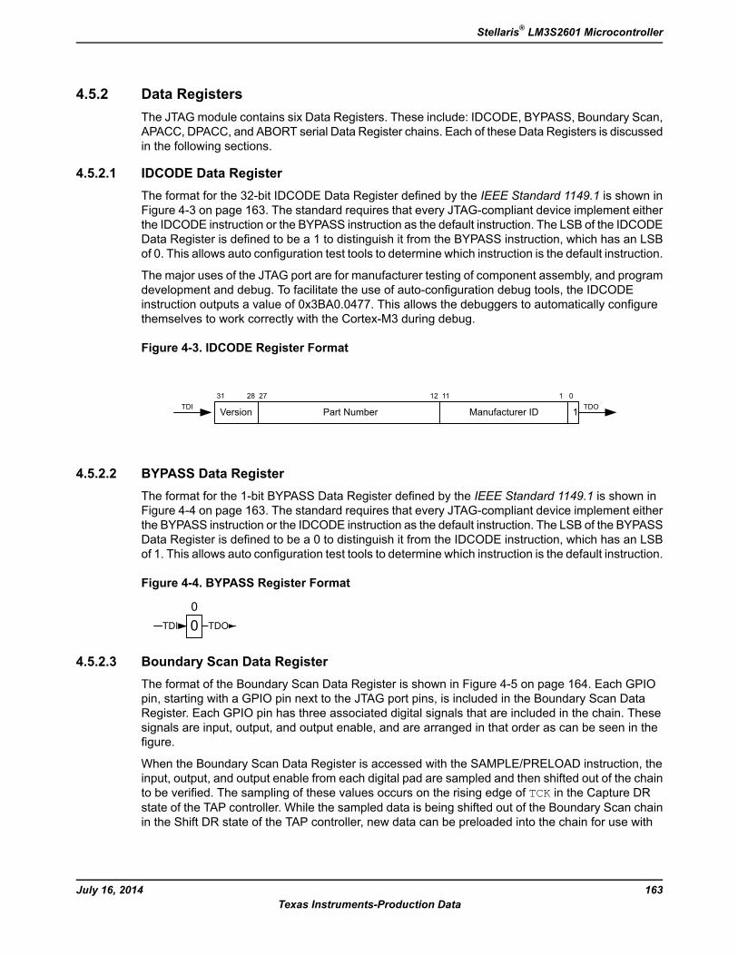
4.5.2 Data RegistersThe JTAGmodule contains six Data Registers. These include: IDCODE, BYPASS, Boundary Scan,APACC, DPACC, and ABORT serial Data Register chains. Each of these Data Registers is discussedin the following sections.
4.5.2.1 IDCODE Data RegisterThe format for the 32-bit IDCODE Data Register defined by the IEEE Standard 1149.1 is shown inFigure 4-3 on page 163. The standard requires that every JTAG-compliant device implement eitherthe IDCODE instruction or the BYPASS instruction as the default instruction. The LSB of the IDCODEData Register is defined to be a 1 to distinguish it from the BYPASS instruction, which has an LSBof 0. This allows auto configuration test tools to determine which instruction is the default instruction.
The major uses of the JTAG port are for manufacturer testing of component assembly, and programdevelopment and debug. To facilitate the use of auto-configuration debug tools, the IDCODEinstruction outputs a value of 0x3BA0.0477. This allows the debuggers to automatically configurethemselves to work correctly with the Cortex-M3 during debug.
Figure 4-3. IDCODE Register Format
Version Part Number Manufacturer ID 1
31 28 27 12 11 1 0TDOTDI
4.5.2.2 BYPASS Data RegisterThe format for the 1-bit BYPASS Data Register defined by the IEEE Standard 1149.1 is shown inFigure 4-4 on page 163. The standard requires that every JTAG-compliant device implement eitherthe BYPASS instruction or the IDCODE instruction as the default instruction. The LSB of the BYPASSData Register is defined to be a 0 to distinguish it from the IDCODE instruction, which has an LSBof 1. This allows auto configuration test tools to determine which instruction is the default instruction.
Figure 4-4. BYPASS Register Format
0 TDOTDI
0
4.5.2.3 Boundary Scan Data RegisterThe format of the Boundary Scan Data Register is shown in Figure 4-5 on page 164. Each GPIOpin, starting with a GPIO pin next to the JTAG port pins, is included in the Boundary Scan DataRegister. Each GPIO pin has three associated digital signals that are included in the chain. Thesesignals are input, output, and output enable, and are arranged in that order as can be seen in thefigure.
When the Boundary Scan Data Register is accessed with the SAMPLE/PRELOAD instruction, theinput, output, and output enable from each digital pad are sampled and then shifted out of the chainto be verified. The sampling of these values occurs on the rising edge of TCK in the Capture DRstate of the TAP controller. While the sampled data is being shifted out of the Boundary Scan chainin the Shift DR state of the TAP controller, new data can be preloaded into the chain for use with
163July 16, 2014Texas Instruments-Production Data
Stellaris® LM3S2601 Microcontroller
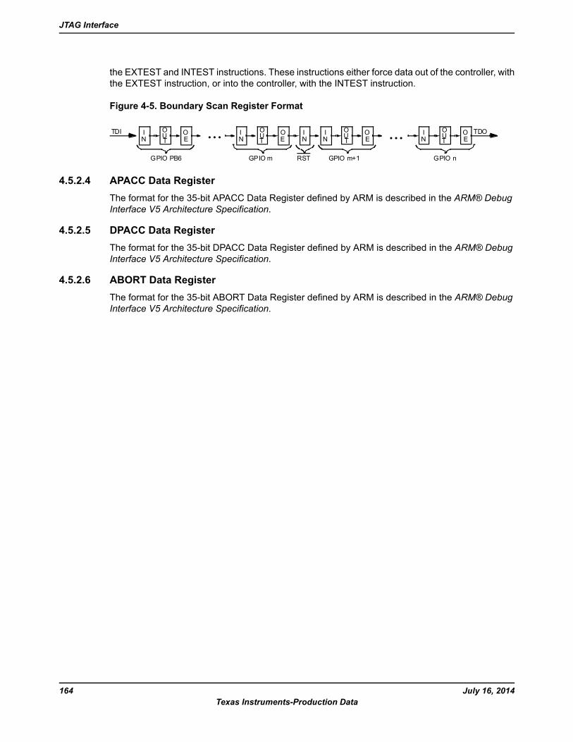
the EXTEST and INTEST instructions. These instructions either force data out of the controller, withthe EXTEST instruction, or into the controller, with the INTEST instruction.
Figure 4-5. Boundary Scan Register Format
O TDOTDI OIN EU
TOOI
N EUT
OOIN EU
TOOI
N EUT
IN... ...
RSTGPIO PB6 GPIO m GPIO m+1 GPIO n
4.5.2.4 APACC Data RegisterThe format for the 35-bit APACC Data Register defined by ARM is described in the ARM® DebugInterface V5 Architecture Specification.
4.5.2.5 DPACC Data RegisterThe format for the 35-bit DPACC Data Register defined by ARM is described in the ARM® DebugInterface V5 Architecture Specification.
4.5.2.6 ABORT Data RegisterThe format for the 35-bit ABORT Data Register defined by ARM is described in the ARM® DebugInterface V5 Architecture Specification.
July 16, 2014164Texas Instruments-Production Data
JTAG Interface
5 System ControlSystem control determines the overall operation of the device. It provides information about thedevice, controls the clocking to the core and individual peripherals, and handles reset detection andreporting.
5.1 Signal DescriptionTable 5-1 on page 165 and Table 5-2 on page 165 list the external signals of the System Controlmodule and describe the function of each. The NMI signal is the alternate function for and functionsas a GPIO after reset. under commit protection and require a special process to be configured asany alternate function or to subsequently return to the GPIO function, see “CommitControl” on page 289. The column in the table below titled "Pin Assignment" lists the GPIO pinplacement for the NMI signal. The AFSEL bit in theGPIO Alternate Function Select (GPIOAFSEL)register (page 302) should be set to choose the NMI function. For more information on configuringGPIOs, see “General-Purpose Input/Outputs (GPIOs)” on page 279. The remaining signals (with theword "fixed" in the Pin Assignment column) have a fixed pin assignment and function.
Table 5-1. System Control & Clocks Signals (100LQFP)
DescriptionBuffer TypeaPin TypePin NumberPin Name
CPUMode bit 0. Input must be set to logic 0 (grounded); otherencodings reserved.
TTLI65CMOD0
CPUMode bit 1. Input must be set to logic 0 (grounded); otherencodings reserved.
TTLI76CMOD1
Main oscillator crystal input or an external clock referenceinput.
AnalogI48OSC0
Main oscillator crystal output. Leave unconnected when usinga single-ended clock source.
AnalogO49OSC1
System reset input.TTLI64RST
a. The TTL designation indicates the pin has TTL-compatible voltage levels.
Table 5-2. System Control & Clocks Signals (108BGA)
DescriptionBuffer TypeaPin TypePin NumberPin Name
CPUMode bit 0. Input must be set to logic 0 (grounded); otherencodings reserved.
TTLIE11CMOD0
CPUMode bit 1. Input must be set to logic 0 (grounded); otherencodings reserved.
TTLIB10CMOD1
Main oscillator crystal input or an external clock referenceinput.
AnalogIL11OSC0
Main oscillator crystal output. Leave unconnected when usinga single-ended clock source.
AnalogOM11OSC1
System reset input.TTLIH11RST
a. The TTL designation indicates the pin has TTL-compatible voltage levels.
5.2 Functional DescriptionThe System Control module provides the following capabilities:
Device identification (see “Device Identification” on page 166)
165July 16, 2014Texas Instruments-Production Data
Stellaris® LM3S2601 Microcontroller
Local control, such as reset (see “Reset Control” on page 166), power (see “PowerControl” on page 170) and clock control (see “Clock Control” on page 171)
System control (Run, Sleep, and Deep-Sleep modes); see “System Control” on page 176
5.2.1 Device IdentificationSeveral read-only registers provide software with information on the microcontroller, such as version,part number, SRAM size, flash size, and other features. See theDID0,DID1, andDC0-DC4 registers.
5.2.2 Reset ControlThis section discusses aspects of hardware functions during reset as well as system softwarerequirements following the reset sequence.
5.2.2.1 CMOD0 and CMOD1 Test-Mode Control PinsTwo pins, CMOD0 and CMOD1, are defined for internal use for testing the microcontroller duringmanufacture. They have no end-user function and should not be used. The CMOD pins should beconnected to ground.
5.2.2.2 Reset SourcesThe controller has five sources of reset:
1. External reset input pin (RST) assertion; see “External RST Pin” on page 167.
2. Power-on reset (POR); see “Power-On Reset (POR)” on page 167.
3. Internal brown-out (BOR) detector; see “Brown-Out Reset (BOR)” on page 168.
4. Software-initiated reset (with the software reset registers); see “Software Reset” on page 169.
5. A watchdog timer reset condition violation; see “Watchdog Timer Reset” on page 169.
Table 5-3 provides a summary of results of the various reset operations.
Table 5-3. Reset Sources
On-Chip Peripherals Reset?JTAG Reset?Core Reset?Reset Source
YesYesYesPower-On Reset
YesPin Config OnlyYesRST
YesNoYesBrown-Out Reset
YesNoYesSoftware System RequestReseta
YesbNoNoSoftware Peripheral Reset
YesNoYesWatchdog Reset
a. By using the SYSRESREQ bit in the ARM Cortex-M3 Application Interrupt and Reset Control (APINT) registerb. Programmable on a module-by-module basis using the Software Reset Control Registers.
After a reset, the Reset Cause (RESC) register is set with the reset cause. The bits in this registerare sticky and maintain their state across multiple reset sequences, except when an internal PORor an external reset is the cause, and then all the other bits in the RESC register are cleared exceptfor the POR or EXT indicator.
July 16, 2014166Texas Instruments-Production Data
System Control
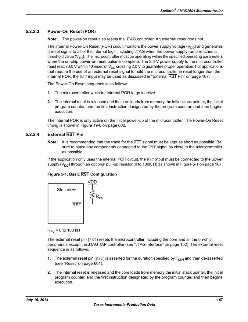
5.2.2.3 Power-On Reset (POR)Note: The power-on reset also resets the JTAG controller. An external reset does not.
The internal Power-On Reset (POR) circuit monitors the power supply voltage (VDD) and generatesa reset signal to all of the internal logic including JTAG when the power supply ramp reaches athreshold value (VTH). Themicrocontroller must be operating within the specified operating parameterswhen the on-chip power-on reset pulse is complete. The 3.3-V power supply to the microcontrollermust reach 3.0 V within 10msec of VDD crossing 2.0 V to guarantee proper operation. For applicationsthat require the use of an external reset signal to hold the microcontroller in reset longer than theinternal POR, the RST input may be used as discussed in “External RST Pin” on page 167.
The Power-On Reset sequence is as follows:
1. The microcontroller waits for internal POR to go inactive.
2. The internal reset is released and the core loads from memory the initial stack pointer, the initialprogram counter, and the first instruction designated by the program counter, and then beginsexecution.
The internal POR is only active on the initial power-up of the microcontroller. The Power-On Resettiming is shown in Figure 19-6 on page 602.
5.2.2.4 External RST PinNote: It is recommended that the trace for the RST signal must be kept as short as possible. Be
sure to place any components connected to the RST signal as close to the microcontrolleras possible.
If the application only uses the internal POR circuit, the RST input must be connected to the powersupply (VDD) through an optional pull-up resistor (0 to 100K Ω) as shown in Figure 5-1 on page 167.
Figure 5-1. Basic RST Configuration
PU
RST
Stellaris®R
VDD
RPU = 0 to 100 kΩ
The external reset pin (RST) resets the microcontroller including the core and all the on-chipperipherals except the JTAG TAP controller (see “JTAG Interface” on page 152). The external resetsequence is as follows:
1. The external reset pin (RST) is asserted for the duration specified by TMIN and then de-asserted(see “Reset” on page 601).
2. The internal reset is released and the core loads from memory the initial stack pointer, the initialprogram counter, and the first instruction designated by the program counter, and then beginsexecution.
167July 16, 2014Texas Instruments-Production Data
Stellaris® LM3S2601 Microcontroller
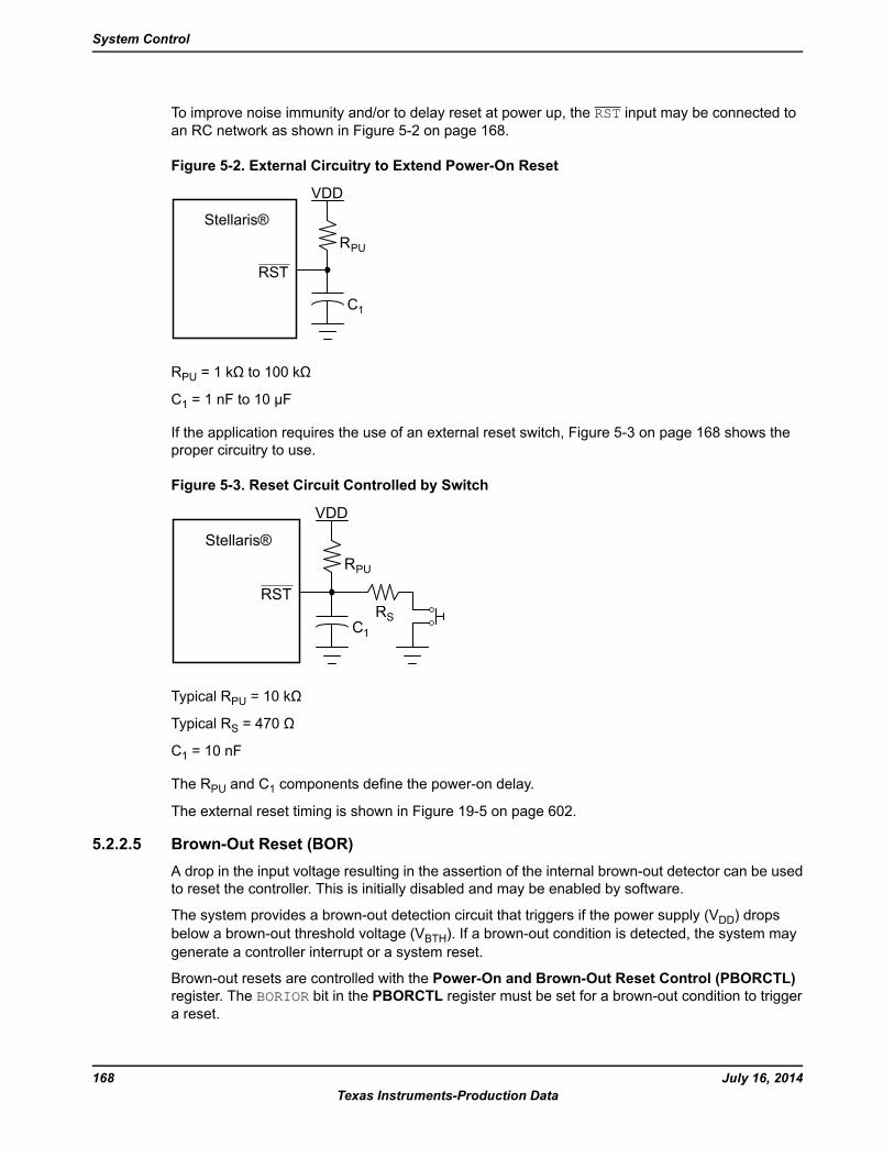
To improve noise immunity and/or to delay reset at power up, the RST input may be connected toan RC network as shown in Figure 5-2 on page 168.
Figure 5-2. External Circuitry to Extend Power-On Reset
PU
C1
RST
Stellaris®R
VDD
RPU = 1 kΩ to 100 kΩ
C1 = 1 nF to 10 µF
If the application requires the use of an external reset switch, Figure 5-3 on page 168 shows theproper circuitry to use.
Figure 5-3. Reset Circuit Controlled by Switch
PU
C1
RS
RST
Stellaris®R
VDD
Typical RPU = 10 kΩ
Typical RS = 470 Ω
C1 = 10 nF
The RPU and C1 components define the power-on delay.
The external reset timing is shown in Figure 19-5 on page 602.
5.2.2.5 Brown-Out Reset (BOR)A drop in the input voltage resulting in the assertion of the internal brown-out detector can be usedto reset the controller. This is initially disabled and may be enabled by software.
The system provides a brown-out detection circuit that triggers if the power supply (VDD) dropsbelow a brown-out threshold voltage (VBTH). If a brown-out condition is detected, the system maygenerate a controller interrupt or a system reset.
Brown-out resets are controlled with the Power-On and Brown-Out Reset Control (PBORCTL)register. The BORIOR bit in the PBORCTL register must be set for a brown-out condition to triggera reset.
July 16, 2014168Texas Instruments-Production Data
System Control
The brown-out reset is equivalent to an assertion of the external RST input and the reset is heldactive until the proper VDD level is restored. TheRESC register can be examined in the reset interrupthandler to determine if a Brown-Out condition was the cause of the reset, thus allowing software todetermine what actions are required to recover.
The internal Brown-Out Reset timing is shown in Figure 19-7 on page 602.
5.2.2.6 Software ResetSoftware can reset a specific peripheral or generate a reset to the entire system .
Peripherals can be individually reset by software via three registers that control reset signals to eachperipheral (see the SRCRn registers). If the bit position corresponding to a peripheral is set andsubsequently cleared, the peripheral is reset. The encoding of the reset registers is consistent withthe encoding of the clock gating control for peripherals and on-chip functions (see “SystemControl” on page 176). Note that all reset signals for all clocks of the specified unit are asserted asa result of a software-initiated reset.
The entire system can be reset by software by setting the SYSRESETREQ bit in the Cortex-M3Application Interrupt and Reset Control register resets the entire system including the core. Thesoftware-initiated system reset sequence is as follows:
1. A software system reset is initiated by writing the SYSRESETREQ bit in the ARM Cortex-M3Application Interrupt and Reset Control register.
2. An internal reset is asserted.
3. The internal reset is deasserted and the controller loads from memory the initial stack pointer,the initial program counter, and the first instruction designated by the program counter, andthen begins execution.
The software-initiated system reset timing is shown in Figure 19-8 on page 603.
5.2.2.7 Watchdog Timer ResetThe watchdog timer module's function is to prevent system hangs. The watchdog timer can beconfigured to generate an interrupt to the controller on its first time-out, and to generate a resetsignal on its second time-out.
After the first time-out event, the 32-bit counter is reloaded with the value of theWatchdog TimerLoad (WDTLOAD) register, and the timer resumes counting down from that value. If the timer countsdown to its zero state again before the first time-out interrupt is cleared, and the reset signal hasbeen enabled, the watchdog timer asserts its reset signal to the system. The watchdog timer resetsequence is as follows:
1. The watchdog timer times out for the second time without being serviced.
2. An internal reset is asserted.
3. The internal reset is released and the controller loads from memory the initial stack pointer, theinitial program counter, the first instruction designated by the program counter, and beginsexecution.
The watchdog reset timing is shown in Figure 19-9 on page 603.
169July 16, 2014Texas Instruments-Production Data
Stellaris® LM3S2601 Microcontroller
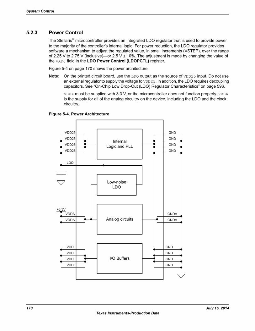
5.2.3 Power ControlThe Stellaris® microcontroller provides an integrated LDO regulator that is used to provide powerto the majority of the controller's internal logic. For power reduction, the LDO regulator providessoftware a mechanism to adjust the regulated value, in small increments (VSTEP), over the rangeof 2.25 V to 2.75 V (inclusive)—or 2.5 V ± 10%. The adjustment is made by changing the value ofthe VADJ field in the LDO Power Control (LDOPCTL) register.
Figure 5-4 on page 170 shows the power architecture.
Note: On the printed circuit board, use the LDO output as the source of VDD25 input. Do not usean external regulator to supply the voltage to VDD25. In addition, the LDO requires decouplingcapacitors. See “On-Chip Low Drop-Out (LDO) Regulator Characteristics” on page 596.
VDDA must be supplied with 3.3 V, or the microcontroller does not function properly. VDDAis the supply for all of the analog circuitry on the device, including the LDO and the clockcircuitry.
Figure 5-4. Power Architecture
I/O Buffers
Analog circuits
Low-noiseLDO
InternalLogic and PLL
GND
GND
GND
GND
GNDA
GND
GND
GND
GND
VDD
VDD
VDD
VDD
VDDA
VDDA
VDD25
VDD25
VDD25
VDD25
LDO
+3.3V
GNDA
July 16, 2014170Texas Instruments-Production Data
System Control
5.2.4 Clock ControlSystem control determines the control of clocks in this part.
5.2.4.1 Fundamental Clock SourcesThere are multiple clock sources for use in the device:
Internal Oscillator (IOSC). The internal oscillator is an on-chip clock source. It does not requirethe use of any external components. The frequency of the internal oscillator is 12 MHz ± 30%.Applications that do not depend on accurate clock sources may use this clock source to reducesystem cost. The internal oscillator is the clock source the device uses during and following POR.If the main oscillator is required, software must enable the main oscillator following reset andallow the main oscillator to stabilize before changing the clock reference.
Main Oscillator (MOSC). The main oscillator provides a frequency-accurate clock source byone of two means: an external single-ended clock source is connected to the OSC0 input pin, oran external crystal is connected across the OSC0 input and OSC1 output pins. If the PLL is beingused, the crystal value must be one of the supported frequencies between 3.579545MHz through8.192 MHz (inclusive). If the PLL is not being used, the crystal may be any one of the supportedfrequencies between 1 MHz and 8.192 MHz. The single-ended clock source range is from DCthrough the specified speed of the device. The supported crystals are listed in the XTAL bit fieldin the RCC register (see page 188).
Internal 30-kHz Oscillator. The internal 30-kHz oscillator is similar to the internal oscillator,except that it provides an operational frequency of 30 kHz ± 50%. It is intended for use duringDeep-Sleep power-saving modes. This power-savings mode benefits from reduced internalswitching and also allows the main oscillator to be powered down.
External Real-Time Oscillator. The external real-time oscillator provides a low-frequency,accurate clock reference. It is intended to provide the system with a real-time clock source. Thereal-time oscillator is part of the Hibernation Module (see “Hibernation Module” on page 231) andmay also provide an accurate source of Deep-Sleep or Hibernate mode power savings.
The internal system clock (SysClk), is derived from any of the above sources plus two others: theoutput of the main internal PLL, and the internal oscillator divided by four (3 MHz ± 30%). Thefrequency of the PLL clock reference must be in the range of 3.579545MHz to 8.192 MHz (inclusive).Table 5-4 on page 171 shows how the various clock sources can be used in a system.
Table 5-4. Clock Source Options
Used as SysClk?Drive PLL?Clock Source
BYPASS = 1, OSCSRC = 0x1YesBYPASS = 1NoInternal Oscillator (12 MHz)
BYPASS = 1, OSCSRC = 0x2YesBYPASS = 1NoInternal Oscillator divide by 4 (3MHz)
BYPASS = 1, OSCSRC = 0x0YesBYPASS = 0, OSCSRC =0x0
YesMain Oscillator
BYPASS = 1, OSCSRC = 0x3YesBYPASS = 1NoInternal 30-kHz Oscillator
BYPASS = 1, OSCSRC2 = 0x7YesBYPASS = 1NoExternal Real-Time Oscillator
5.2.4.2 Clock ConfigurationThe Run-Mode Clock Configuration (RCC) and Run-Mode Clock Configuration 2 (RCC2)registers provide control for the system clock. The RCC2 register is provided to extend fields that
171July 16, 2014Texas Instruments-Production Data
Stellaris® LM3S2601 Microcontroller
offer additional encodings over the RCC register. When used, the RCC2 register field values areused by the logic over the corresponding field in the RCC register. In particular, RCC2 provides fora larger assortment of clock configuration options. These registers control the following clockfunctionality:
Source of clocks in sleep and deep-sleep modes
System clock derived from PLL or other clock source
Enabling/disabling of oscillators and PLL
Clock divisors
Crystal input selection
Figure 5-5 on page 173 shows the logic for the main clock tree. The peripheral blocks are driven bythe system clock signal and can be individually enabled/disabled.
July 16, 2014172Texas Instruments-Production Data
System Control
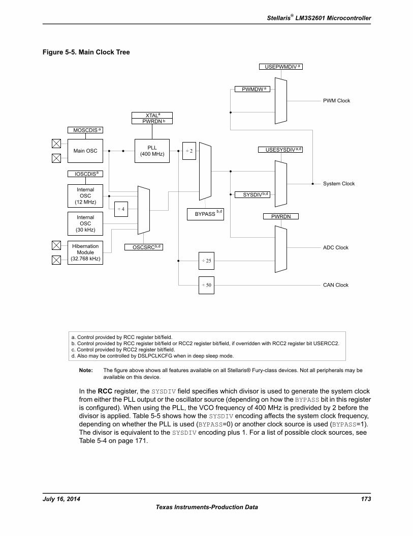
Figure 5-5. Main Clock Tree
PLL(400 MHz)Main OSC
InternalOSC
(12 MHz)
InternalOSC
(30 kHz)
÷ 4
HibernationModule
(32.768 kHz) ÷ 25
PWRDN
ADC Clock
System Clock
XTALaPWRDN b
MOSCDIS a
IOSCDISa
OSCSRCb,d
BYPASS b,d
SYSDIVb,d
USESYSDIVa,d
PWMDW a
USEPWMDIV a
PWM Clock
a. Control provided by RCC register bit/field.b. Control provided by RCC register bit/field or RCC2 register bit/field, if overridden with RCC2 register bit USERCC2.c. Control provided by RCC2 register bit/field.d. Also may be controlled by DSLPCLKCFG when in deep sleep mode.
÷ 2
÷ 50 CAN Clock
Note: The figure above shows all features available on all Stellaris® Fury-class devices. Not all peripherals may beavailable on this device.
In the RCC register, the SYSDIV field specifies which divisor is used to generate the system clockfrom either the PLL output or the oscillator source (depending on how the BYPASS bit in this registeris configured). When using the PLL, the VCO frequency of 400 MHz is predivided by 2 before thedivisor is applied. Table 5-5 shows how the SYSDIV encoding affects the system clock frequency,depending on whether the PLL is used (BYPASS=0) or another clock source is used (BYPASS=1).The divisor is equivalent to the SYSDIV encoding plus 1. For a list of possible clock sources, seeTable 5-4 on page 171.
173July 16, 2014Texas Instruments-Production Data
Stellaris® LM3S2601 Microcontroller
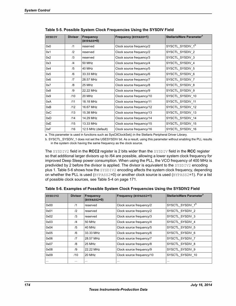
Table 5-5. Possible System Clock Frequencies Using the SYSDIV Field
StellarisWare ParameteraFrequency (BYPASS=1)Frequency(BYPASS=0)
DivisorSYSDIV
SYSCTL_SYSDIV_1bClock source frequency/2reserved/10x0
SYSCTL_SYSDIV_2Clock source frequency/2reserved/20x1
SYSCTL_SYSDIV_3Clock source frequency/3reserved/30x2
SYSCTL_SYSDIV_4Clock source frequency/450 MHz/40x3
SYSCTL_SYSDIV_5Clock source frequency/540 MHz/50x4
SYSCTL_SYSDIV_6Clock source frequency/633.33 MHz/60x5
SYSCTL_SYSDIV_7Clock source frequency/728.57 MHz/70x6
SYSCTL_SYSDIV_8Clock source frequency/825 MHz/80x7
SYSCTL_SYSDIV_9Clock source frequency/922.22 MHz/90x8
SYSCTL_SYSDIV_10Clock source frequency/1020 MHz/100x9
SYSCTL_SYSDIV_11Clock source frequency/1118.18 MHz/110xA
SYSCTL_SYSDIV_12Clock source frequency/1216.67 MHz/120xB
SYSCTL_SYSDIV_13Clock source frequency/1315.38 MHz/130xC
SYSCTL_SYSDIV_14Clock source frequency/1414.29 MHz/140xD
SYSCTL_SYSDIV_15Clock source frequency/1513.33 MHz/150xE
SYSCTL_SYSDIV_16Clock source frequency/1612.5 MHz (default)/160xF
a. This parameter is used in functions such as SysCtlClockSet() in the Stellaris Peripheral Driver Library.b. SYSCTL_SYSDIV_1 does not set the USESYSDIV bit. As a result, using this parameter without enabling the PLL results
in the system clock having the same frequency as the clock source.
The SYSDIV2 field in the RCC2 register is 2 bits wider than the SYSDIV field in the RCC registerso that additional larger divisors up to /64 are possible, allowing a lower system clock frequency forimproved Deep Sleep power consumption. When using the PLL, the VCO frequency of 400 MHz ispredivided by 2 before the divisor is applied. The divisor is equivalent to the SYSDIV2 encodingplus 1. Table 5-6 shows how the SYSDIV2 encoding affects the system clock frequency, dependingon whether the PLL is used (BYPASS2=0) or another clock source is used (BYPASS2=1). For a listof possible clock sources, see Table 5-4 on page 171.
Table 5-6. Examples of Possible System Clock Frequencies Using the SYSDIV2 Field
StellarisWare ParameteraFrequency (BYPASS2=1)Frequency(BYPASS2=0)
DivisorSYSDIV2
SYSCTL_SYSDIV_1bClock source frequency/2reserved/10x00
SYSCTL_SYSDIV_2Clock source frequency/2reserved/20x01
SYSCTL_SYSDIV_3Clock source frequency/3reserved/30x02
SYSCTL_SYSDIV_4Clock source frequency/450 MHz/40x03
SYSCTL_SYSDIV_5Clock source frequency/540 MHz/50x04
SYSCTL_SYSDIV_6Clock source frequency/633.33 MHz/60x05
SYSCTL_SYSDIV_7Clock source frequency/728.57 MHz/70x06
SYSCTL_SYSDIV_8Clock source frequency/825 MHz/80x07
SYSCTL_SYSDIV_9Clock source frequency/922.22 MHz/90x08
SYSCTL_SYSDIV_10Clock source frequency/1020 MHz/100x09
...............
July 16, 2014174Texas Instruments-Production Data
System Control
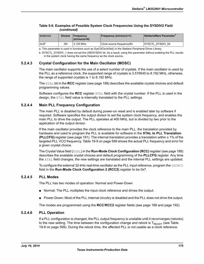
Table 5-6. Examples of Possible System Clock Frequencies Using the SYSDIV2 Field(continued)
StellarisWare ParameteraFrequency (BYPASS2=1)Frequency(BYPASS2=0)
DivisorSYSDIV2
SYSCTL_SYSDIV_64Clock source frequency/643.125 MHz/640x3F
a. This parameter is used in functions such as SysCtlClockSet() in the Stellaris Peripheral Driver Library.b. SYSCTL_SYSDIV_1 does not set the USESYSDIV bit. As a result, using this parameter without enabling the PLL results
in the system clock having the same frequency as the clock source.
5.2.4.3 Crystal Configuration for the Main Oscillator (MOSC)The main oscillator supports the use of a select number of crystals. If the main oscillator is used bythe PLL as a reference clock, the supported range of crystals is 3.579545 to 8.192 MHz, otherwise,the range of supported crystals is 1 to 8.192 MHz.
The XTAL bit in the RCC register (see page 188) describes the available crystal choices and defaultprogramming values.
Software configures the RCC register XTAL field with the crystal number. If the PLL is used in thedesign, the XTAL field value is internally translated to the PLL settings.
5.2.4.4 Main PLL Frequency ConfigurationThe main PLL is disabled by default during power-on reset and is enabled later by software ifrequired. Software specifies the output divisor to set the system clock frequency, and enables themain PLL to drive the output. The PLL operates at 400 MHz, but is divided by two prior to theapplication of the output divisor.
If the main oscillator provides the clock reference to the main PLL, the translation provided byhardware and used to program the PLL is available for software in the XTAL to PLL Translation(PLLCFG) register (see page 191). The internal translation provides a translation within ± 1% of thetargeted PLL VCO frequency. Table 19-9 on page 599 shows the actual PLL frequency and error fora given crystal choice.
The Crystal Value field (XTAL) in theRun-Mode Clock Configuration (RCC) register (see page 188)describes the available crystal choices and default programming of the PLLCFG register. Any timethe XTAL field changes, the new settings are translated and the internal PLL settings are updated.
To configure the external 32-kHz real-time oscillator as the PLL input reference, program the OSCRC2field in the Run-Mode Clock Configuration 2 (RCC2) register to be 0x7.
5.2.4.5 PLL ModesThe PLL has two modes of operation: Normal and Power-Down
Normal: The PLL multiplies the input clock reference and drives the output.
Power-Down: Most of the PLL internal circuitry is disabled and the PLL does not drive the output.
The modes are programmed using the RCC/RCC2 register fields (see page 188 and page 192).
5.2.4.6 PLL OperationIf a PLL configuration is changed, the PLL output frequency is unstable until it reconverges (relocks)to the new setting. The time between the configuration change and relock is TREADY (see Table19-8 on page 599). During the relock time, the affected PLL is not usable as a clock reference.
175July 16, 2014Texas Instruments-Production Data
Stellaris® LM3S2601 Microcontroller
PLL is changed by one of the following:
Change to the XTAL value in the RCC register—writes of the same value do not cause a relock.
Change in the PLL from Power-Down to Normal mode.
A counter is defined to measure the TREADY requirement. The counter is clocked by the mainoscillator. The range of the main oscillator has been taken into account and the down counter is setto 0x1200 (that is, ~600 μs at an 8.192 MHz external oscillator clock). Hardware is provided to keepthe PLL from being used as a system clock until the TREADY condition is met after one of the twochanges above. It is the user's responsibility to have a stable clock source (like the main oscillator)before the RCC/RCC2 register is switched to use the PLL.
If the main PLL is enabled and the system clock is switched to use the PLL in one step, the systemcontrol hardware continues to clock the controller from the oscillator selected by the RCC/RCC2register until the main PLL is stable (TREADY time met), after which it changes to the PLL. Softwarecan use many methods to ensure that the system is clocked from the main PLL, including periodicallypolling the PLLLRIS bit in the Raw Interrupt Status (RIS) register, and enabling the PLL Lockinterrupt.
5.2.5 System ControlFor power-savings purposes, the RCGCn , SCGCn , and DCGCn registers control the clock gatinglogic for each peripheral or block in the system while the controller is in Run, Sleep, and Deep-Sleepmode, respectively.
There are four levels of operation for the device defined as:
Run Mode. In Run mode, the controller actively executes code. Run mode provides normaloperation of the processor and all of the peripherals that are currently enabled by the RCGCnregisters. The system clock can be any of the available clock sources including the PLL.
Sleep Mode. In Sleep mode, the clock frequency of the active peripherals is unchanged, but theprocessor and the memory subsystem are not clocked and therefore no longer execute code.Sleep mode is entered by the Cortex-M3 core executing a WFI(Wait for Interrupt)instruction. Any properly configured interrupt event in the system will bring the processor backinto Run mode. See “Power Management” on page 83 for more details.
Peripherals are clocked that are enabled in theSCGCn register when auto-clock gating is enabled(see theRCC register) or theRCGCn register when the auto-clock gating is disabled. The systemclock has the same source and frequency as that during Run mode.
Deep-Sleep Mode. In Deep-Sleep mode, the clock frequency of the active peripherals maychange (depending on the Run mode clock configuration) in addition to the processor clock beingstopped. An interrupt returns the device to Run mode from one of the sleep modes; the sleepmodes are entered on request from the code. Deep-Sleep mode is entered by first writing theDeep Sleep Enable bit in the ARM Cortex-M3 NVIC system control register and then executinga WFI instruction. Any properly configured interrupt event in the system will bring the processorback into Run mode. See “Power Management” on page 83 for more details.
The Cortex-M3 processor core and the memory subsystem are not clocked. Peripherals areclocked that are enabled in theDCGCn register when auto-clock gating is enabled (see theRCCregister) or the RCGCn register when auto-clock gating is disabled. The system clock source isthe main oscillator by default or the internal oscillator specified in the DSLPCLKCFG register ifone is enabled. When the DSLPCLKCFG register is used, the internal oscillator is powered up,if necessary, and the main oscillator is powered down. If the PLL is running at the time of the
July 16, 2014176Texas Instruments-Production Data
System Control
WFI instruction, hardware will power the PLL down and override the SYSDIV field of the activeRCC/RCC2 register, to be determined by the DSDIVORIDE setting in theDSLPCLKCFG register,up to /16 or /64 respectively. When the Deep-Sleep exit event occurs, hardware brings the systemclock back to the source and frequency it had at the onset of Deep-Sleep mode before enablingthe clocks that had been stopped during the Deep-Sleep duration.
Hibernate Mode. In this mode, the power supplies are turned off to the main part of the deviceand only the Hibernation module's circuitry is active. An external wake event or RTC event isrequired to bring the device back to Runmode. The Cortex-M3 processor and peripherals outsideof the Hibernation module see a normal "power on" sequence and the processor starts runningcode. It can determine that it has been restarted from Hibernate mode by inspecting theHibernation module registers.
Caution – If the Cortex-M3 Debug Access Port (DAP) has been enabled, and the device wakes from alow power sleep or deep-sleep mode, the core may start executing code before all clocks to peripheralshave been restored to their run mode configuration. The DAP is usually enabled by software toolsaccessing the JTAG or SWD interface when debugging or flash programming. If this condition occurs,a Hard Fault is triggered when software accesses a peripheral with an invalid clock.
A software delay loop can be used at the beginning of the interrupt routine that is used to wake up asystem from aWFI (Wait For Interrupt) instruction. This stalls the execution of any code that accessesa peripheral register that might cause a fault. This loop can be removed for production software as theDAP is most likely not enabled during normal execution.
Because the DAP is disabled by default (power on reset), the user can also power-cycle the device. TheDAP is not enabled unless it is enabled through the JTAG or SWD interface.
5.3 Initialization and ConfigurationThe PLL is configured using direct register writes to the RCC/RCC2 register. If the RCC2 registeris being used, the USERCC2 bit must be set and the appropriate RCC2 bit/field is used. The stepsrequired to successfully change the PLL-based system clock are:
1. Bypass the PLL and system clock divider by setting the BYPASS bit and clearing the USESYSbit in the RCC register. This configures the system to run off a “raw” clock source and allowsfor the new PLL configuration to be validated before switching the system clock to the PLL.
2. Select the crystal value (XTAL) and oscillator source (OSCSRC), and clear the PWRDN bit inRCC/RCC2. Setting the XTAL field automatically pulls valid PLL configuration data for theappropriate crystal, and clearing the PWRDN bit powers and enables the PLL and its output.
3. Select the desired system divider (SYSDIV) in RCC/RCC2 and set the USESYS bit in RCC. TheSYSDIV field determines the system frequency for the microcontroller.
4. Wait for the PLL to lock by polling the PLLLRIS bit in the Raw Interrupt Status (RIS) register.
5. Enable use of the PLL by clearing the BYPASS bit in RCC/RCC2.
5.4 Register MapTable 5-7 on page 178 lists the System Control registers, grouped by function. The offset listed is ahexadecimal increment to the register's address, relative to the System Control base address of0x400F.E000.
177July 16, 2014Texas Instruments-Production Data
Stellaris® LM3S2601 Microcontroller
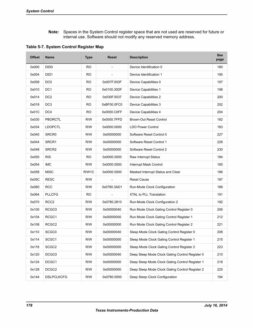
Note: Spaces in the System Control register space that are not used are reserved for future orinternal use. Software should not modify any reserved memory address.
Table 5-7. System Control Register Map
SeepageDescriptionResetTypeNameOffset
180Device Identification 0-RODID00x000
195Device Identification 1-RODID10x004
197Device Capabilities 00x007F.003FRODC00x008
198Device Capabilities 10x0100.30DFRODC10x010
200Device Capabilities 20x030F.5037RODC20x014
202Device Capabilities 30xBF00.0FC0RODC30x018
204Device Capabilities 40x0000.C0FFRODC40x01C
182Brown-Out Reset Control0x0000.7FFDR/WPBORCTL0x030
183LDO Power Control0x0000.0000R/WLDOPCTL0x034
227Software Reset Control 00x00000000R/WSRCR00x040
228Software Reset Control 10x00000000R/WSRCR10x044
230Software Reset Control 20x00000000R/WSRCR20x048
184Raw Interrupt Status0x0000.0000RORIS0x050
185Interrupt Mask Control0x0000.0000R/WIMC0x054
186Masked Interrupt Status and Clear0x0000.0000R/W1CMISC0x058
187Reset Cause-R/WRESC0x05C
188Run-Mode Clock Configuration0x0780.3AD1R/WRCC0x060
191XTAL to PLL Translation-ROPLLCFG0x064
192Run-Mode Clock Configuration 20x0780.2810R/WRCC20x070
206Run Mode Clock Gating Control Register 00x00000040R/WRCGC00x100
212Run Mode Clock Gating Control Register 10x00000000R/WRCGC10x104
221Run Mode Clock Gating Control Register 20x00000000R/WRCGC20x108
208Sleep Mode Clock Gating Control Register 00x00000040R/WSCGC00x110
215Sleep Mode Clock Gating Control Register 10x00000000R/WSCGC10x114
223Sleep Mode Clock Gating Control Register 20x00000000R/WSCGC20x118
210Deep Sleep Mode Clock Gating Control Register 00x00000040R/WDCGC00x120
218Deep Sleep Mode Clock Gating Control Register 10x00000000R/WDCGC10x124
225Deep Sleep Mode Clock Gating Control Register 20x00000000R/WDCGC20x128
194Deep Sleep Clock Configuration0x0780.0000R/WDSLPCLKCFG0x144
July 16, 2014178Texas Instruments-Production Data
System Control
5.5 Register DescriptionsAll addresses given are relative to the System Control base address of 0x400F.E000.
179July 16, 2014Texas Instruments-Production Data
Stellaris® LM3S2601 Microcontroller
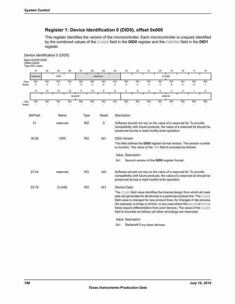
Register 1: Device Identification 0 (DID0), offset 0x000This register identifies the version of the microcontroller. Each microcontroller is uniquely identifiedby the combined values of the CLASS field in the DID0 register and the PARTNO field in the DID1register.
Device Identification 0 (DID0)Base 0x400F.E000Offset 0x000Type RO, reset -
16171819202122232425262728293031
CLASSreservedVERreserved
ROROROROROROROROROROROROROROROROType1000000000001000Reset
0123456789101112131415
MINORMAJOR
ROROROROROROROROROROROROROROROROType----------------Reset
DescriptionResetTypeNameBit/Field
Software should not rely on the value of a reserved bit. To providecompatibility with future products, the value of a reserved bit should bepreserved across a read-modify-write operation.
0ROreserved31
DID0 VersionThis field defines the DID0 register format version. The version numberis numeric. The value of the VER field is encoded as follows:
DescriptionValue
Second version of the DID0 register format.0x1
0x1ROVER30:28
Software should not rely on the value of a reserved bit. To providecompatibility with future products, the value of a reserved bit should bepreserved across a read-modify-write operation.
0x0ROreserved27:24
Device ClassThe CLASS field value identifies the internal design from which all masksets are generated for all devices in a particular product line. The CLASSfield value is changed for new product lines, for changes in fab process(for example, a remap or shrink), or any case where the MAJOR or MINORfields require differentiation from prior devices. The value of the CLASSfield is encoded as follows (all other encodings are reserved):
DescriptionValue
Stellaris® Fury-class devices.0x1
0x1ROCLASS23:16
July 16, 2014180Texas Instruments-Production Data
System Control
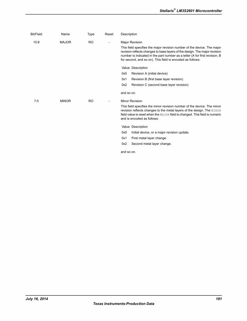
DescriptionResetTypeNameBit/Field
Major RevisionThis field specifies the major revision number of the device. The majorrevision reflects changes to base layers of the design. Themajor revisionnumber is indicated in the part number as a letter (A for first revision, Bfor second, and so on). This field is encoded as follows:
DescriptionValue
Revision A (initial device)0x0
Revision B (first base layer revision)0x1
Revision C (second base layer revision)0x2
and so on.
-ROMAJOR15:8
Minor RevisionThis field specifies the minor revision number of the device. The minorrevision reflects changes to the metal layers of the design. The MINORfield value is reset when the MAJOR field is changed. This field is numericand is encoded as follows:
DescriptionValue
Initial device, or a major revision update.0x0
First metal layer change.0x1
Second metal layer change.0x2
and so on.
-ROMINOR7:0
181July 16, 2014Texas Instruments-Production Data
Stellaris® LM3S2601 Microcontroller
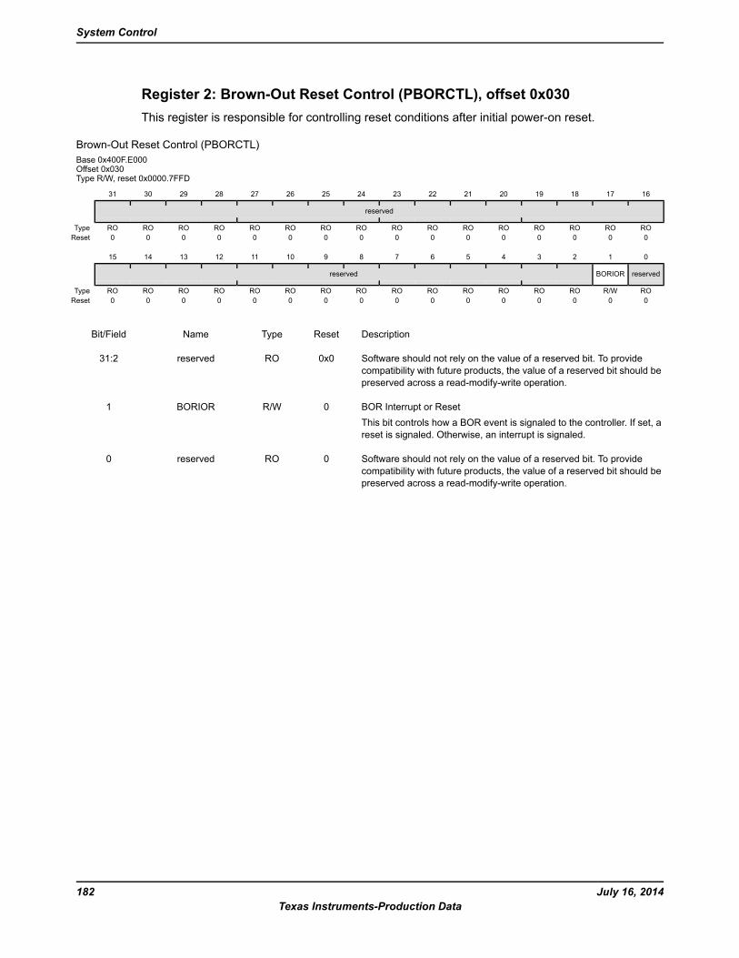
Register 2: Brown-Out Reset Control (PBORCTL), offset 0x030This register is responsible for controlling reset conditions after initial power-on reset.
Brown-Out Reset Control (PBORCTL)Base 0x400F.E000Offset 0x030Type R/W, reset 0x0000.7FFD
16171819202122232425262728293031
reserved
ROROROROROROROROROROROROROROROROType0000000000000000Reset
0123456789101112131415
reservedBORIORreserved
ROR/WROROROROROROROROROROROROROROType0000000000000000Reset
DescriptionResetTypeNameBit/Field
Software should not rely on the value of a reserved bit. To providecompatibility with future products, the value of a reserved bit should bepreserved across a read-modify-write operation.
0x0ROreserved31:2
BOR Interrupt or ResetThis bit controls how a BOR event is signaled to the controller. If set, areset is signaled. Otherwise, an interrupt is signaled.
0R/WBORIOR1
Software should not rely on the value of a reserved bit. To providecompatibility with future products, the value of a reserved bit should bepreserved across a read-modify-write operation.
0ROreserved0
July 16, 2014182Texas Instruments-Production Data
System Control
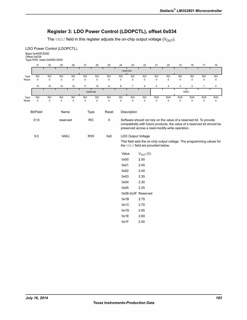
Register 3: LDO Power Control (LDOPCTL), offset 0x034The VADJ field in this register adjusts the on-chip output voltage (VOUT).
LDO Power Control (LDOPCTL)Base 0x400F.E000Offset 0x034Type R/W, reset 0x0000.0000
16171819202122232425262728293031
reserved
ROROROROROROROROROROROROROROROROType0000000000000000Reset
0123456789101112131415
VADJreserved
R/WR/WR/WR/WR/WR/WROROROROROROROROROROType0000000000000000Reset
DescriptionResetTypeNameBit/Field
Software should not rely on the value of a reserved bit. To providecompatibility with future products, the value of a reserved bit should bepreserved across a read-modify-write operation.
0ROreserved31:6
LDO Output VoltageThis field sets the on-chip output voltage. The programming values forthe VADJ field are provided below.
VOUT (V)Value
2.500x00
2.450x01
2.400x02
2.350x03
2.300x04
2.250x05
Reserved0x06-0x3F
2.750x1B
2.700x1C
2.650x1D
2.600x1E
2.550x1F
0x0R/WVADJ5:0
183July 16, 2014Texas Instruments-Production Data
Stellaris® LM3S2601 Microcontroller
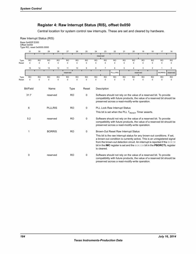
Register 4: Raw Interrupt Status (RIS), offset 0x050Central location for system control raw interrupts. These are set and cleared by hardware.
Raw Interrupt Status (RIS)Base 0x400F.E000Offset 0x050Type RO, reset 0x0000.0000
16171819202122232425262728293031
reserved
ROROROROROROROROROROROROROROROROType0000000000000000Reset
0123456789101112131415
reservedBORRISreservedPLLLRISreserved
ROROROROROROROROROROROROROROROROType0000000000000000Reset
DescriptionResetTypeNameBit/Field
Software should not rely on the value of a reserved bit. To providecompatibility with future products, the value of a reserved bit should bepreserved across a read-modify-write operation.
0ROreserved31:7
PLL Lock Raw Interrupt StatusThis bit is set when the PLL TREADY Timer asserts.
0ROPLLLRIS6
Software should not rely on the value of a reserved bit. To providecompatibility with future products, the value of a reserved bit should bepreserved across a read-modify-write operation.
0ROreserved5:2
Brown-Out Reset Raw Interrupt StatusThis bit is the raw interrupt status for any brown-out conditions. If set,a brown-out condition is currently active. This is an unregistered signalfrom the brown-out detection circuit. An interrupt is reported if the BORIMbit in the IMC register is set and the BORIOR bit in the PBORCTL registeris cleared.
0ROBORRIS1
Software should not rely on the value of a reserved bit. To providecompatibility with future products, the value of a reserved bit should bepreserved across a read-modify-write operation.
0ROreserved0
July 16, 2014184Texas Instruments-Production Data
System Control
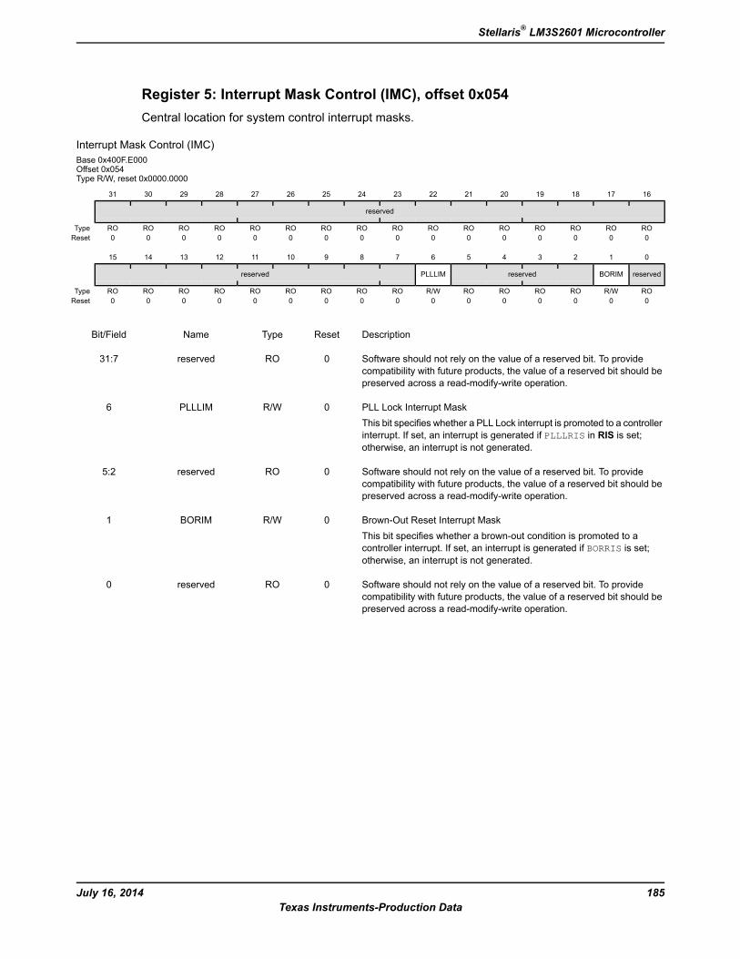
Register 5: Interrupt Mask Control (IMC), offset 0x054Central location for system control interrupt masks.
Interrupt Mask Control (IMC)Base 0x400F.E000Offset 0x054Type R/W, reset 0x0000.0000
16171819202122232425262728293031
reserved
ROROROROROROROROROROROROROROROROType0000000000000000Reset
0123456789101112131415
reservedBORIMreservedPLLLIMreserved
ROR/WROROROROR/WROROROROROROROROROType0000000000000000Reset
DescriptionResetTypeNameBit/Field
Software should not rely on the value of a reserved bit. To providecompatibility with future products, the value of a reserved bit should bepreserved across a read-modify-write operation.
0ROreserved31:7
PLL Lock Interrupt MaskThis bit specifies whether a PLL Lock interrupt is promoted to a controllerinterrupt. If set, an interrupt is generated if PLLLRIS in RIS is set;otherwise, an interrupt is not generated.
0R/WPLLLIM6
Software should not rely on the value of a reserved bit. To providecompatibility with future products, the value of a reserved bit should bepreserved across a read-modify-write operation.
0ROreserved5:2
Brown-Out Reset Interrupt MaskThis bit specifies whether a brown-out condition is promoted to acontroller interrupt. If set, an interrupt is generated if BORRIS is set;otherwise, an interrupt is not generated.
0R/WBORIM1
Software should not rely on the value of a reserved bit. To providecompatibility with future products, the value of a reserved bit should bepreserved across a read-modify-write operation.
0ROreserved0
185July 16, 2014Texas Instruments-Production Data
Stellaris® LM3S2601 Microcontroller
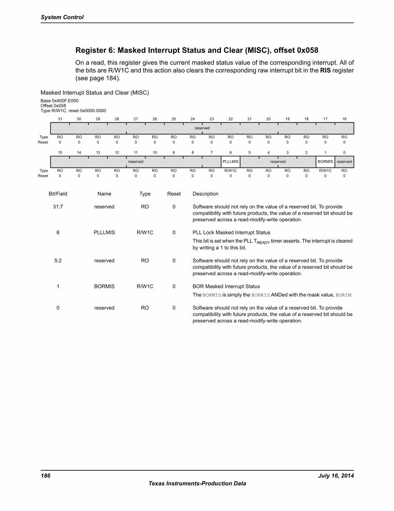
Register 6: Masked Interrupt Status and Clear (MISC), offset 0x058On a read, this register gives the current masked status value of the corresponding interrupt. All ofthe bits are R/W1C and this action also clears the corresponding raw interrupt bit in the RIS register(see page 184).
Masked Interrupt Status and Clear (MISC)Base 0x400F.E000Offset 0x058Type R/W1C, reset 0x0000.0000
16171819202122232425262728293031
reserved
ROROROROROROROROROROROROROROROROType0000000000000000Reset
0123456789101112131415
reservedBORMISreservedPLLLMISreserved
ROR/W1CROROROROR/W1CROROROROROROROROROType0000000000000000Reset
DescriptionResetTypeNameBit/Field
Software should not rely on the value of a reserved bit. To providecompatibility with future products, the value of a reserved bit should bepreserved across a read-modify-write operation.
0ROreserved31:7
PLL Lock Masked Interrupt StatusThis bit is set when the PLL TREADY timer asserts. The interrupt is clearedby writing a 1 to this bit.
0R/W1CPLLLMIS6
Software should not rely on the value of a reserved bit. To providecompatibility with future products, the value of a reserved bit should bepreserved across a read-modify-write operation.
0ROreserved5:2
BOR Masked Interrupt StatusThe BORMIS is simply the BORRIS ANDed with the mask value, BORIM.
0R/W1CBORMIS1
Software should not rely on the value of a reserved bit. To providecompatibility with future products, the value of a reserved bit should bepreserved across a read-modify-write operation.
0ROreserved0
July 16, 2014186Texas Instruments-Production Data
System Control
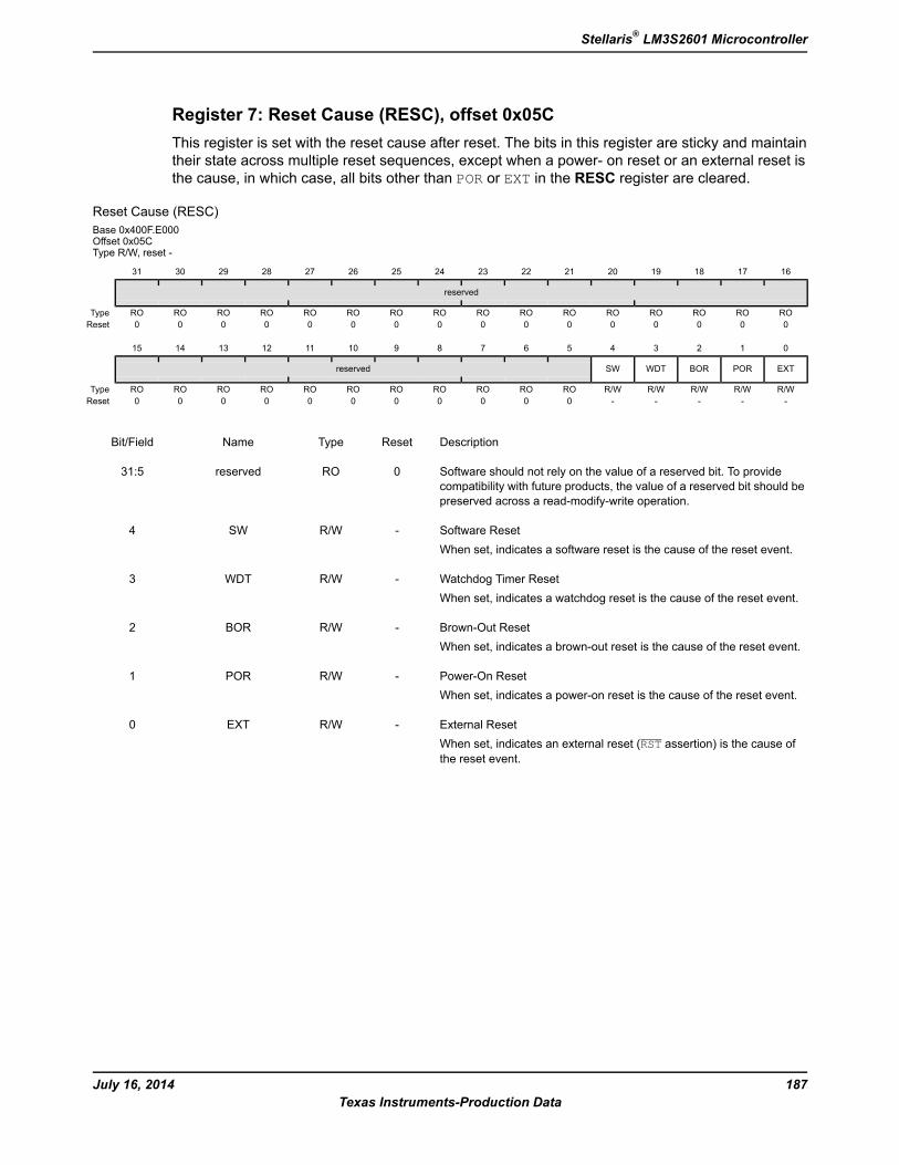
Register 7: Reset Cause (RESC), offset 0x05CThis register is set with the reset cause after reset. The bits in this register are sticky and maintaintheir state across multiple reset sequences, except when a power- on reset or an external reset isthe cause, in which case, all bits other than POR or EXT in the RESC register are cleared.
Reset Cause (RESC)Base 0x400F.E000Offset 0x05CType R/W, reset -
16171819202122232425262728293031
reserved
ROROROROROROROROROROROROROROROROType0000000000000000Reset
0123456789101112131415
EXTPORBORWDTSWreserved
R/WR/WR/WR/WR/WROROROROROROROROROROROType-----00000000000Reset
DescriptionResetTypeNameBit/Field
Software should not rely on the value of a reserved bit. To providecompatibility with future products, the value of a reserved bit should bepreserved across a read-modify-write operation.
0ROreserved31:5
Software ResetWhen set, indicates a software reset is the cause of the reset event.
-R/WSW4
Watchdog Timer ResetWhen set, indicates a watchdog reset is the cause of the reset event.
-R/WWDT3
Brown-Out ResetWhen set, indicates a brown-out reset is the cause of the reset event.
-R/WBOR2
Power-On ResetWhen set, indicates a power-on reset is the cause of the reset event.
-R/WPOR1
External ResetWhen set, indicates an external reset (RST assertion) is the cause ofthe reset event.
-R/WEXT0
187July 16, 2014Texas Instruments-Production Data
Stellaris® LM3S2601 Microcontroller
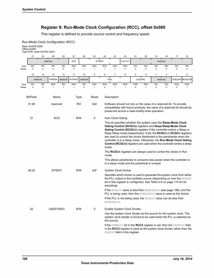
Register 8: Run-Mode Clock Configuration (RCC), offset 0x060This register is defined to provide source control and frequency speed.
Run-Mode Clock Configuration (RCC)Base 0x400F.E000Offset 0x060Type R/W, reset 0x0780.3AD1
16171819202122232425262728293031
reservedUSESYSDIVSYSDIVACGreserved
ROROROROROROR/WR/WR/WR/WR/WR/WROROROROType0000000111100000Reset
0123456789101112131415
MOSCDISIOSCDISreservedOSCSRCXTALreservedBYPASSreservedPWRDNreserved
R/WR/WROROR/WR/WR/WR/WR/WR/WROR/WROR/WROROType1000101101011100Reset
DescriptionResetTypeNameBit/Field
Software should not rely on the value of a reserved bit. To providecompatibility with future products, the value of a reserved bit should bepreserved across a read-modify-write operation.
0x0ROreserved31:28
Auto Clock GatingThis bit specifies whether the system uses the Sleep-Mode ClockGating Control (SCGCn) registers and Deep-Sleep-Mode ClockGating Control (DCGCn) registers if the controller enters a Sleep orDeep-Sleep mode (respectively). If set, the SCGCn orDCGCn registersare used to control the clocks distributed to the peripherals when thecontroller is in a sleep mode. Otherwise, the Run-Mode Clock GatingControl (RCGCn) registers are used when the controller enters a sleepmode.The RCGCn registers are always used to control the clocks in Runmode.This allows peripherals to consume less power when the controller isin a sleep mode and the peripheral is unused.
0R/WACG27
System Clock DivisorSpecifies which divisor is used to generate the system clock from eitherthe PLL output or the oscillator source (depending on how the BYPASSbit in this register is configured). See Table 5-5 on page 174 for bitencodings.If the SYSDIV value is less than MINSYSDIV (see page 198), and thePLL is being used, then the MINSYSDIV value is used as the divisor.If the PLL is not being used, the SYSDIV value can be less thanMINSYSDIV.
0xFR/WSYSDIV26:23
Enable System Clock DividerUse the system clock divider as the source for the system clock. Thesystem clock divider is forced to be used when the PLL is selected asthe source.If the USERCC2 bit in the RCC2 register is set, then the SYSDIV2 fieldin the RCC2 register is used as the system clock divider rather than theSYSDIV field in this register.
0R/WUSESYSDIV22
July 16, 2014188Texas Instruments-Production Data
System Control
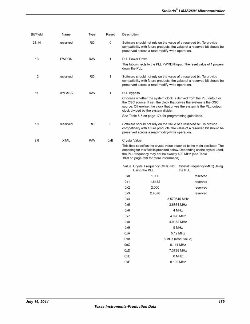
DescriptionResetTypeNameBit/Field
Software should not rely on the value of a reserved bit. To providecompatibility with future products, the value of a reserved bit should bepreserved across a read-modify-write operation.
0ROreserved21:14
PLL Power DownThis bit connects to the PLL PWRDN input. The reset value of 1 powersdown the PLL.
1R/WPWRDN13
Software should not rely on the value of a reserved bit. To providecompatibility with future products, the value of a reserved bit should bepreserved across a read-modify-write operation.
1ROreserved12
PLL BypassChooses whether the system clock is derived from the PLL output orthe OSC source. If set, the clock that drives the system is the OSCsource. Otherwise, the clock that drives the system is the PLL outputclock divided by the system divider.See Table 5-5 on page 174 for programming guidelines.
1R/WBYPASS11
Software should not rely on the value of a reserved bit. To providecompatibility with future products, the value of a reserved bit should bepreserved across a read-modify-write operation.
0ROreserved10
Crystal ValueThis field specifies the crystal value attached to the main oscillator. Theencoding for this field is provided below. Depending on the crystal used,the PLL frequency may not be exactly 400 MHz (see Table19-9 on page 599 for more information).
Crystal Frequency (MHz) Usingthe PLL
Crystal Frequency (MHz) NotUsing the PLL
Value
reserved1.0000x0
reserved1.84320x1
reserved2.0000x2
reserved2.45760x3
3.579545 MHz0x4
3.6864 MHz0x5
4 MHz0x6
4.096 MHz0x7
4.9152 MHz0x8
5 MHz0x9
5.12 MHz0xA
6 MHz (reset value)0xB
6.144 MHz0xC
7.3728 MHz0xD
8 MHz0xE
8.192 MHz0xF
0xBR/WXTAL9:6
189July 16, 2014Texas Instruments-Production Data
Stellaris® LM3S2601 Microcontroller
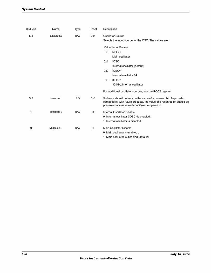
DescriptionResetTypeNameBit/Field
Oscillator SourceSelects the input source for the OSC. The values are:
Input SourceValue
MOSCMain oscillator
0x0
IOSCInternal oscillator (default)
0x1
IOSC/4Internal oscillator / 4
0x2
30 kHz30-KHz internal oscillator
0x3
For additional oscillator sources, see the RCC2 register.
0x1R/WOSCSRC5:4
Software should not rely on the value of a reserved bit. To providecompatibility with future products, the value of a reserved bit should bepreserved across a read-modify-write operation.
0x0ROreserved3:2
Internal Oscillator Disable0: Internal oscillator (IOSC) is enabled.1: Internal oscillator is disabled.
0R/WIOSCDIS1
Main Oscillator Disable0: Main oscillator is enabled .1: Main oscillator is disabled (default).
1R/WMOSCDIS0
July 16, 2014190Texas Instruments-Production Data
System Control
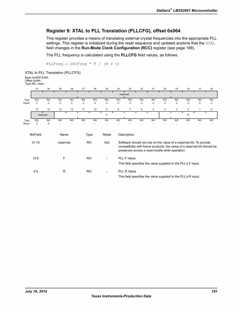
Register 9: XTAL to PLL Translation (PLLCFG), offset 0x064This register provides a means of translating external crystal frequencies into the appropriate PLLsettings. This register is initialized during the reset sequence and updated anytime that the XTALfield changes in the Run-Mode Clock Configuration (RCC) register (see page 188).
The PLL frequency is calculated using the PLLCFG field values, as follows:
PLLFreq = OSCFreq * F / (R + 1)
XTAL to PLL Translation (PLLCFG)Base 0x400F.E000Offset 0x064Type RO, reset -
16171819202122232425262728293031
reserved
ROROROROROROROROROROROROROROROROType0000000000000000Reset
0123456789101112131415
RFreserved
ROROROROROROROROROROROROROROROROType--------------00Reset
DescriptionResetTypeNameBit/Field
Software should not rely on the value of a reserved bit. To providecompatibility with future products, the value of a reserved bit should bepreserved across a read-modify-write operation.
0x0ROreserved31:14
PLL F ValueThis field specifies the value supplied to the PLL’s F input.
-ROF13:5
PLL R ValueThis field specifies the value supplied to the PLL’s R input.
-ROR4:0
191July 16, 2014Texas Instruments-Production Data
Stellaris® LM3S2601 Microcontroller
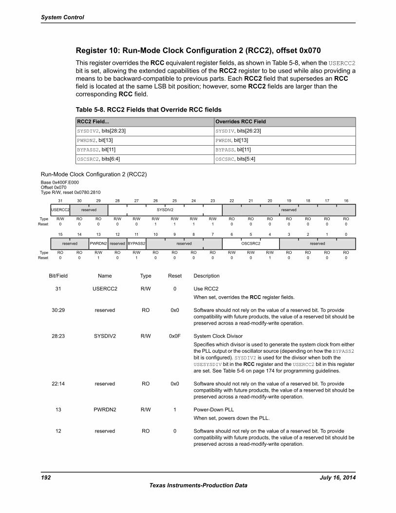
Register 10: Run-Mode Clock Configuration 2 (RCC2), offset 0x070This register overrides theRCC equivalent register fields, as shown in Table 5-8, when the USERCC2bit is set, allowing the extended capabilities of the RCC2 register to be used while also providing ameans to be backward-compatible to previous parts. Each RCC2 field that supersedes an RCCfield is located at the same LSB bit position; however, some RCC2 fields are larger than thecorresponding RCC field.
Table 5-8. RCC2 Fields that Override RCC fields
Overrides RCC FieldRCC2 Field...
SYSDIV, bits[26:23]SYSDIV2, bits[28:23]
PWRDN, bit[13]PWRDN2, bit[13]
BYPASS, bit[11]BYPASS2, bit[11]
OSCSRC, bits[5:4]OSCSRC2, bits[6:4]
Run-Mode Clock Configuration 2 (RCC2)Base 0x400F.E000Offset 0x070Type R/W, reset 0x0780.2810
16171819202122232425262728293031
reservedSYSDIV2reservedUSERCC2
ROROROROROROROR/WR/WR/WR/WR/WR/WROROR/WType0000000111100000Reset
0123456789101112131415
reservedOSCSRC2reservedBYPASS2reservedPWRDN2reserved
ROROROROR/WR/WR/WROROROROR/WROR/WROROType0000100000010100Reset
DescriptionResetTypeNameBit/Field
Use RCC2When set, overrides the RCC register fields.
0R/WUSERCC231
Software should not rely on the value of a reserved bit. To providecompatibility with future products, the value of a reserved bit should bepreserved across a read-modify-write operation.
0x0ROreserved30:29
System Clock DivisorSpecifies which divisor is used to generate the system clock from eitherthe PLL output or the oscillator source (depending on how the BYPASS2bit is configured). SYSDIV2 is used for the divisor when both theUSESYSDIV bit in the RCC register and the USERCC2 bit in this registerare set. See Table 5-6 on page 174 for programming guidelines.
0x0FR/WSYSDIV228:23
Software should not rely on the value of a reserved bit. To providecompatibility with future products, the value of a reserved bit should bepreserved across a read-modify-write operation.
0x0ROreserved22:14
Power-Down PLLWhen set, powers down the PLL.
1R/WPWRDN213
Software should not rely on the value of a reserved bit. To providecompatibility with future products, the value of a reserved bit should bepreserved across a read-modify-write operation.
0ROreserved12
July 16, 2014192Texas Instruments-Production Data
System Control
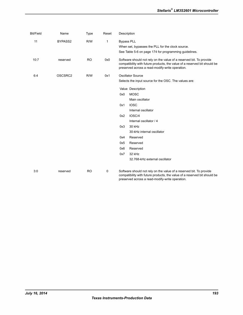
DescriptionResetTypeNameBit/Field
Bypass PLLWhen set, bypasses the PLL for the clock source.See Table 5-6 on page 174 for programming guidelines.
1R/WBYPASS211
Software should not rely on the value of a reserved bit. To providecompatibility with future products, the value of a reserved bit should bepreserved across a read-modify-write operation.
0x0ROreserved10:7
Oscillator SourceSelects the input source for the OSC. The values are:
DescriptionValue
MOSCMain oscillator
0x0
IOSCInternal oscillator
0x1
IOSC/4Internal oscillator / 4
0x2
30 kHz30-kHz internal oscillator
0x3
Reserved0x4
Reserved0x5
Reserved0x6
32 kHz32.768-kHz external oscillator
0x7
0x1R/WOSCSRC26:4
Software should not rely on the value of a reserved bit. To providecompatibility with future products, the value of a reserved bit should bepreserved across a read-modify-write operation.
0ROreserved3:0
193July 16, 2014Texas Instruments-Production Data
Stellaris® LM3S2601 Microcontroller
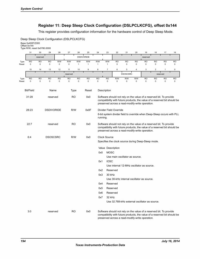
Register 11: Deep Sleep Clock Configuration (DSLPCLKCFG), offset 0x144This register provides configuration information for the hardware control of Deep Sleep Mode.
Deep Sleep Clock Configuration (DSLPCLKCFG)Base 0x400F.E000Offset 0x144Type R/W, reset 0x0780.0000
16171819202122232425262728293031
reservedDSDIVORIDEreserved
ROROROROROROROR/WR/WR/WR/WR/WR/WROROROType0000000111100000Reset
0123456789101112131415
reservedDSOSCSRCreserved
ROROROROR/WR/WR/WROROROROROROROROROType0000000000000000Reset
DescriptionResetTypeNameBit/Field
Software should not rely on the value of a reserved bit. To providecompatibility with future products, the value of a reserved bit should bepreserved across a read-modify-write operation.
0x0ROreserved31:29
Divider Field Override6-bit system divider field to override when Deep-Sleep occurs with PLLrunning.
0x0FR/WDSDIVORIDE28:23
Software should not rely on the value of a reserved bit. To providecompatibility with future products, the value of a reserved bit should bepreserved across a read-modify-write operation.
0x0ROreserved22:7
Clock SourceSpecifies the clock source during Deep-Sleep mode.
DescriptionValue
MOSCUse main oscillator as source.
0x0
IOSCUse internal 12-MHz oscillator as source.
0x1
Reserved0x2
30 kHzUse 30-kHz internal oscillator as source.
0x3
Reserved0x4
Reserved0x5
Reserved0x6
32 kHzUse 32.768-kHz external oscillator as source.
0x7
0x0R/WDSOSCSRC6:4
Software should not rely on the value of a reserved bit. To providecompatibility with future products, the value of a reserved bit should bepreserved across a read-modify-write operation.
0x0ROreserved3:0
July 16, 2014194Texas Instruments-Production Data
System Control
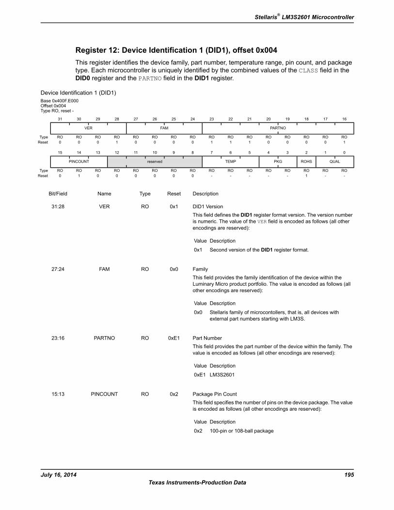
Register 12: Device Identification 1 (DID1), offset 0x004This register identifies the device family, part number, temperature range, pin count, and packagetype. Each microcontroller is uniquely identified by the combined values of the CLASS field in theDID0 register and the PARTNO field in the DID1 register.
Device Identification 1 (DID1)Base 0x400F.E000Offset 0x004Type RO, reset -
16171819202122232425262728293031
PARTNOFAMVER
ROROROROROROROROROROROROROROROROType1000011100001000Reset
0123456789101112131415
QUALROHSPKGTEMPreservedPINCOUNT
ROROROROROROROROROROROROROROROROType--1-----00000010Reset
DescriptionResetTypeNameBit/Field
DID1 VersionThis field defines the DID1 register format version. The version numberis numeric. The value of the VER field is encoded as follows (all otherencodings are reserved):
DescriptionValue
Second version of the DID1 register format.0x1
0x1ROVER31:28
FamilyThis field provides the family identification of the device within theLuminary Micro product portfolio. The value is encoded as follows (allother encodings are reserved):
DescriptionValue
Stellaris family of microcontollers, that is, all devices withexternal part numbers starting with LM3S.
0x0
0x0ROFAM27:24
Part NumberThis field provides the part number of the device within the family. Thevalue is encoded as follows (all other encodings are reserved):
DescriptionValue
LM3S26010xE1
0xE1ROPARTNO23:16
Package Pin CountThis field specifies the number of pins on the device package. The valueis encoded as follows (all other encodings are reserved):
DescriptionValue
100-pin or 108-ball package0x2
0x2ROPINCOUNT15:13
195July 16, 2014Texas Instruments-Production Data
Stellaris® LM3S2601 Microcontroller
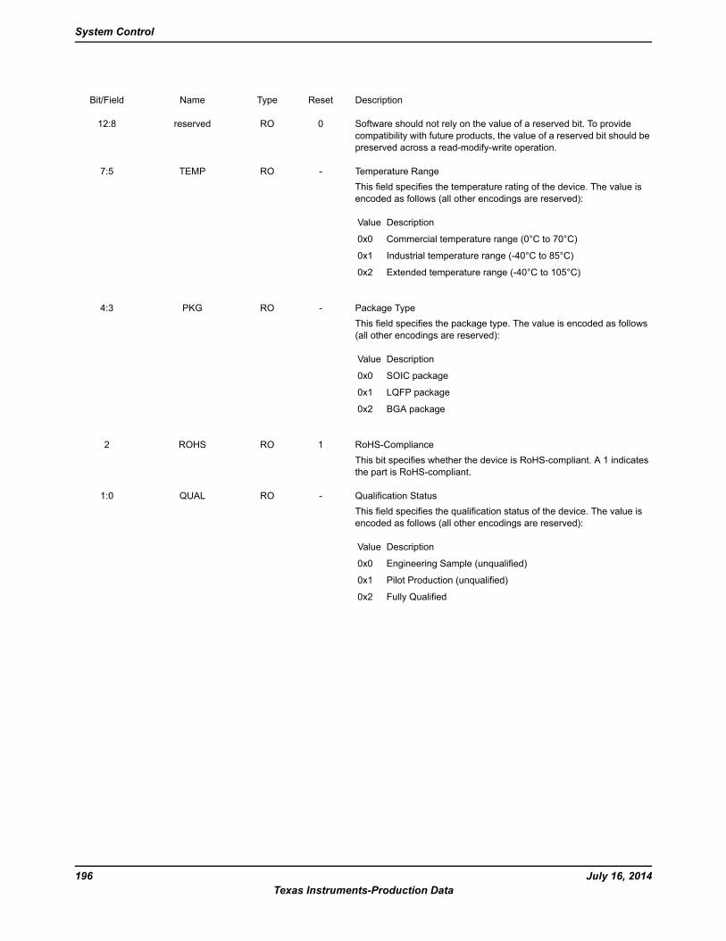
DescriptionResetTypeNameBit/Field
Software should not rely on the value of a reserved bit. To providecompatibility with future products, the value of a reserved bit should bepreserved across a read-modify-write operation.
0ROreserved12:8
Temperature RangeThis field specifies the temperature rating of the device. The value isencoded as follows (all other encodings are reserved):
DescriptionValue
Commercial temperature range (0°C to 70°C)0x0
Industrial temperature range (-40°C to 85°C)0x1
Extended temperature range (-40°C to 105°C)0x2
-ROTEMP7:5
Package TypeThis field specifies the package type. The value is encoded as follows(all other encodings are reserved):
DescriptionValue
SOIC package0x0
LQFP package0x1
BGA package0x2
-ROPKG4:3
RoHS-ComplianceThis bit specifies whether the device is RoHS-compliant. A 1 indicatesthe part is RoHS-compliant.
1ROROHS2
Qualification StatusThis field specifies the qualification status of the device. The value isencoded as follows (all other encodings are reserved):
DescriptionValue
Engineering Sample (unqualified)0x0
Pilot Production (unqualified)0x1
Fully Qualified0x2
-ROQUAL1:0
July 16, 2014196Texas Instruments-Production Data
System Control
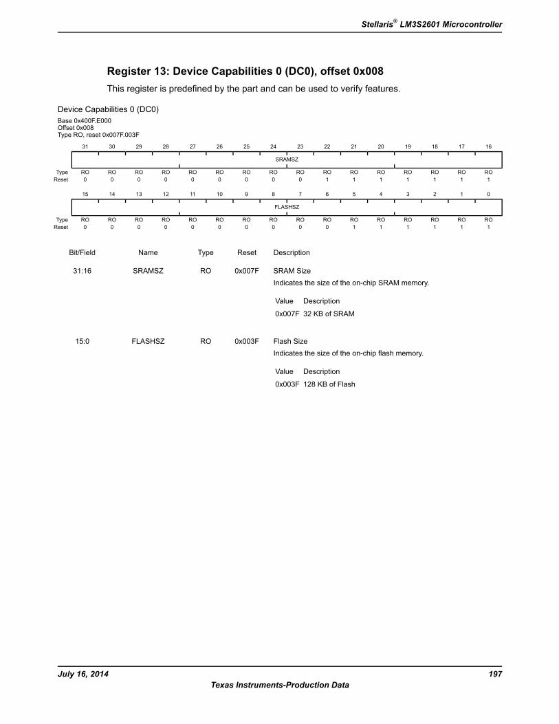
Register 13: Device Capabilities 0 (DC0), offset 0x008This register is predefined by the part and can be used to verify features.
Device Capabilities 0 (DC0)Base 0x400F.E000Offset 0x008Type RO, reset 0x007F.003F
16171819202122232425262728293031
SRAMSZ
ROROROROROROROROROROROROROROROROType1111111000000000Reset
0123456789101112131415
FLASHSZ
ROROROROROROROROROROROROROROROROType1111110000000000Reset
DescriptionResetTypeNameBit/Field
SRAM SizeIndicates the size of the on-chip SRAM memory.
DescriptionValue
32 KB of SRAM0x007F
0x007FROSRAMSZ31:16
Flash SizeIndicates the size of the on-chip flash memory.
DescriptionValue
128 KB of Flash0x003F
0x003FROFLASHSZ15:0
197July 16, 2014Texas Instruments-Production Data
Stellaris® LM3S2601 Microcontroller
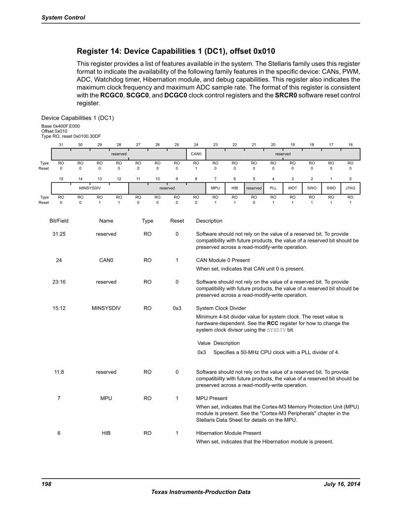
Register 14: Device Capabilities 1 (DC1), offset 0x010This register provides a list of features available in the system. The Stellaris family uses this registerformat to indicate the availability of the following family features in the specific device: CANs, PWM,ADC, Watchdog timer, Hibernation module, and debug capabilities. This register also indicates themaximum clock frequency and maximum ADC sample rate. The format of this register is consistentwith theRCGC0, SCGC0, andDCGC0 clock control registers and theSRCR0 software reset controlregister.
Device Capabilities 1 (DC1)Base 0x400F.E000Offset 0x010Type RO, reset 0x0100.30DF
16171819202122232425262728293031
reservedCAN0reserved
ROROROROROROROROROROROROROROROROType0000000010000000Reset
0123456789101112131415
JTAGSWDSWOWDTPLLreservedHIBMPUreservedMINSYSDIV
ROROROROROROROROROROROROROROROROType1111101100001100Reset
DescriptionResetTypeNameBit/Field
Software should not rely on the value of a reserved bit. To providecompatibility with future products, the value of a reserved bit should bepreserved across a read-modify-write operation.
0ROreserved31:25
CAN Module 0 PresentWhen set, indicates that CAN unit 0 is present.
1ROCAN024
Software should not rely on the value of a reserved bit. To providecompatibility with future products, the value of a reserved bit should bepreserved across a read-modify-write operation.
0ROreserved23:16
System Clock DividerMinimum 4-bit divider value for system clock. The reset value ishardware-dependent. See the RCC register for how to change thesystem clock divisor using the SYSDIV bit.
DescriptionValue
Specifies a 50-MHz CPU clock with a PLL divider of 4.0x3
0x3ROMINSYSDIV15:12
Software should not rely on the value of a reserved bit. To providecompatibility with future products, the value of a reserved bit should bepreserved across a read-modify-write operation.
0ROreserved11:8
MPU PresentWhen set, indicates that the Cortex-M3 Memory Protection Unit (MPU)module is present. See the "Cortex-M3 Peripherals" chapter in theStellaris Data Sheet for details on the MPU.
1ROMPU7
Hibernation Module PresentWhen set, indicates that the Hibernation module is present.
1ROHIB6
July 16, 2014198Texas Instruments-Production Data
System Control
DescriptionResetTypeNameBit/Field
Software should not rely on the value of a reserved bit. To providecompatibility with future products, the value of a reserved bit should bepreserved across a read-modify-write operation.
0ROreserved5
PLL PresentWhen set, indicates that the on-chip Phase Locked Loop (PLL) ispresent.
1ROPLL4
Watchdog Timer PresentWhen set, indicates that a watchdog timer is present.
1ROWDT3
SWO Trace Port PresentWhen set, indicates that the Serial Wire Output (SWO) trace port ispresent.
1ROSWO2
SWD PresentWhen set, indicates that the Serial Wire Debugger (SWD) is present.
1ROSWD1
JTAG PresentWhen set, indicates that the JTAG debugger interface is present.
1ROJTAG0
199July 16, 2014Texas Instruments-Production Data
Stellaris® LM3S2601 Microcontroller
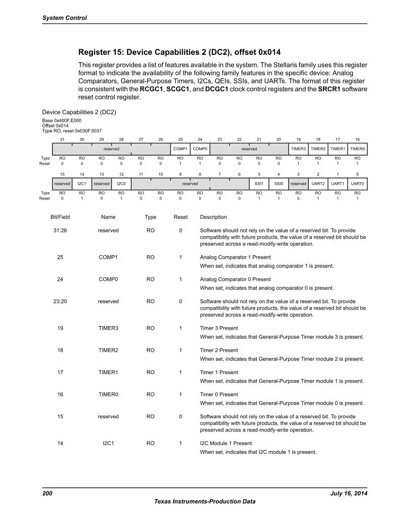
Register 15: Device Capabilities 2 (DC2), offset 0x014This register provides a list of features available in the system. The Stellaris family uses this registerformat to indicate the availability of the following family features in the specific device: AnalogComparators, General-Purpose Timers, I2Cs, QEIs, SSIs, and UARTs. The format of this registeris consistent with theRCGC1, SCGC1, andDCGC1 clock control registers and theSRCR1 softwarereset control register.
Device Capabilities 2 (DC2)Base 0x400F.E000Offset 0x014Type RO, reset 0x030F.5037
16171819202122232425262728293031
TIMER0TIMER1TIMER2TIMER3reservedCOMP0COMP1reserved
ROROROROROROROROROROROROROROROROType1111000011000000Reset
0123456789101112131415
UART0UART1UART2reservedSSI0SSI1reservedI2C0reservedI2C1reserved
ROROROROROROROROROROROROROROROROType1110110000001010Reset
DescriptionResetTypeNameBit/Field
Software should not rely on the value of a reserved bit. To providecompatibility with future products, the value of a reserved bit should bepreserved across a read-modify-write operation.
0ROreserved31:26
Analog Comparator 1 PresentWhen set, indicates that analog comparator 1 is present.
1ROCOMP125
Analog Comparator 0 PresentWhen set, indicates that analog comparator 0 is present.
1ROCOMP024
Software should not rely on the value of a reserved bit. To providecompatibility with future products, the value of a reserved bit should bepreserved across a read-modify-write operation.
0ROreserved23:20
Timer 3 PresentWhen set, indicates that General-Purpose Timer module 3 is present.
1ROTIMER319
Timer 2 PresentWhen set, indicates that General-Purpose Timer module 2 is present.
1ROTIMER218
Timer 1 PresentWhen set, indicates that General-Purpose Timer module 1 is present.
1ROTIMER117
Timer 0 PresentWhen set, indicates that General-Purpose Timer module 0 is present.
1ROTIMER016
Software should not rely on the value of a reserved bit. To providecompatibility with future products, the value of a reserved bit should bepreserved across a read-modify-write operation.
0ROreserved15
I2C Module 1 PresentWhen set, indicates that I2C module 1 is present.
1ROI2C114
July 16, 2014200Texas Instruments-Production Data
System Control
DescriptionResetTypeNameBit/Field
Software should not rely on the value of a reserved bit. To providecompatibility with future products, the value of a reserved bit should bepreserved across a read-modify-write operation.
0ROreserved13
I2C Module 0 PresentWhen set, indicates that I2C module 0 is present.
1ROI2C012
Software should not rely on the value of a reserved bit. To providecompatibility with future products, the value of a reserved bit should bepreserved across a read-modify-write operation.
0ROreserved11:6
SSI1 PresentWhen set, indicates that SSI module 1 is present.
1ROSSI15
SSI0 PresentWhen set, indicates that SSI module 0 is present.
1ROSSI04
Software should not rely on the value of a reserved bit. To providecompatibility with future products, the value of a reserved bit should bepreserved across a read-modify-write operation.
0ROreserved3
UART2 PresentWhen set, indicates that UART module 2 is present.
1ROUART22
UART1 PresentWhen set, indicates that UART module 1 is present.
1ROUART11
UART0 PresentWhen set, indicates that UART module 0 is present.
1ROUART00
201July 16, 2014Texas Instruments-Production Data
Stellaris® LM3S2601 Microcontroller
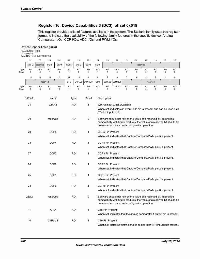
Register 16: Device Capabilities 3 (DC3), offset 0x018This register provides a list of features available in the system. The Stellaris family uses this registerformat to indicate the availability of the following family features in the specific device: AnalogComparator I/Os, CCP I/Os, ADC I/Os, and PWM I/Os.
Device Capabilities 3 (DC3)Base 0x400F.E000Offset 0x018Type RO, reset 0xBF00.0FC0
16171819202122232425262728293031
reservedCCP0CCP1CCP2CCP3CCP4CCP5reserved32KHZ
ROROROROROROROROROROROROROROROROType0000000011111101Reset
0123456789101112131415
reservedC0MINUSC0PLUSC0OC1MINUSC1PLUSC1Oreserved
ROROROROROROROROROROROROROROROROType0000001111110000Reset
DescriptionResetTypeNameBit/Field
32KHz Input Clock AvailableWhen set, indicates an even CCP pin is present and can be used as a32-KHz input clock.
1RO32KHZ31
Software should not rely on the value of a reserved bit. To providecompatibility with future products, the value of a reserved bit should bepreserved across a read-modify-write operation.
0ROreserved30
CCP5 Pin PresentWhen set, indicates that Capture/Compare/PWM pin 5 is present.
1ROCCP529
CCP4 Pin PresentWhen set, indicates that Capture/Compare/PWM pin 4 is present.
1ROCCP428
CCP3 Pin PresentWhen set, indicates that Capture/Compare/PWM pin 3 is present.
1ROCCP327
CCP2 Pin PresentWhen set, indicates that Capture/Compare/PWM pin 2 is present.
1ROCCP226
CCP1 Pin PresentWhen set, indicates that Capture/Compare/PWM pin 1 is present.
1ROCCP125
CCP0 Pin PresentWhen set, indicates that Capture/Compare/PWM pin 0 is present.
1ROCCP024
Software should not rely on the value of a reserved bit. To providecompatibility with future products, the value of a reserved bit should bepreserved across a read-modify-write operation.
0ROreserved23:12
C1o Pin PresentWhen set, indicates that the analog comparator 1 output pin is present.
1ROC1O11
C1+ Pin PresentWhen set, indicates that the analog comparator 1 (+) input pin is present.
1ROC1PLUS10
July 16, 2014202Texas Instruments-Production Data
System Control
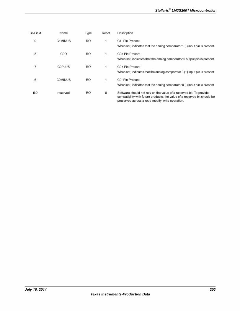
DescriptionResetTypeNameBit/Field
C1- Pin PresentWhen set, indicates that the analog comparator 1 (-) input pin is present.
1ROC1MINUS9
C0o Pin PresentWhen set, indicates that the analog comparator 0 output pin is present.
1ROC0O8
C0+ Pin PresentWhen set, indicates that the analog comparator 0 (+) input pin is present.
1ROC0PLUS7
C0- Pin PresentWhen set, indicates that the analog comparator 0 (-) input pin is present.
1ROC0MINUS6
Software should not rely on the value of a reserved bit. To providecompatibility with future products, the value of a reserved bit should bepreserved across a read-modify-write operation.
0ROreserved5:0
203July 16, 2014Texas Instruments-Production Data
Stellaris® LM3S2601 Microcontroller
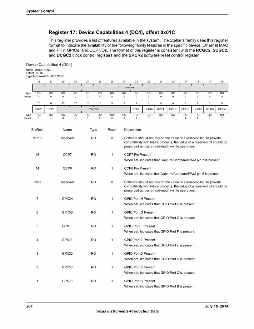
Register 17: Device Capabilities 4 (DC4), offset 0x01CThis register provides a list of features available in the system. The Stellaris family uses this registerformat to indicate the availability of the following family features in the specific device: Ethernet MACand PHY, GPIOs, and CCP I/Os. The format of this register is consistent with the RCGC2, SCGC2,and DCGC2 clock control registers and the SRCR2 software reset control register.
Device Capabilities 4 (DC4)Base 0x400F.E000Offset 0x01CType RO, reset 0x0000.C0FF
16171819202122232425262728293031
reserved
ROROROROROROROROROROROROROROROROType0000000000000000Reset
0123456789101112131415
GPIOAGPIOBGPIOCGPIODGPIOEGPIOFGPIOGGPIOHreservedCCP6CCP7
ROROROROROROROROROROROROROROROROType1111111100000011Reset
DescriptionResetTypeNameBit/Field
Software should not rely on the value of a reserved bit. To providecompatibility with future products, the value of a reserved bit should bepreserved across a read-modify-write operation.
0ROreserved31:16
CCP7 Pin PresentWhen set, indicates that Capture/Compare/PWM pin 7 is present.
1ROCCP715
CCP6 Pin PresentWhen set, indicates that Capture/Compare/PWM pin 6 is present.
1ROCCP614
Software should not rely on the value of a reserved bit. To providecompatibility with future products, the value of a reserved bit should bepreserved across a read-modify-write operation.
0ROreserved13:8
GPIO Port H PresentWhen set, indicates that GPIO Port H is present.
1ROGPIOH7
GPIO Port G PresentWhen set, indicates that GPIO Port G is present.
1ROGPIOG6
GPIO Port F PresentWhen set, indicates that GPIO Port F is present.
1ROGPIOF5
GPIO Port E PresentWhen set, indicates that GPIO Port E is present.
1ROGPIOE4
GPIO Port D PresentWhen set, indicates that GPIO Port D is present.
1ROGPIOD3
GPIO Port C PresentWhen set, indicates that GPIO Port C is present.
1ROGPIOC2
GPIO Port B PresentWhen set, indicates that GPIO Port B is present.
1ROGPIOB1
July 16, 2014204Texas Instruments-Production Data
System Control

DescriptionResetTypeNameBit/Field
GPIO Port A PresentWhen set, indicates that GPIO Port A is present.
1ROGPIOA0
205July 16, 2014Texas Instruments-Production Data
Stellaris® LM3S2601 Microcontroller

Register 18: RunMode Clock Gating Control Register 0 (RCGC0), offset 0x100This register controls the clock gating logic. Each bit controls a clock enable for a given interface,function, or unit. If set, the unit receives a clock and functions. Otherwise, the unit is unclocked anddisabled (saving power). If the unit is unclocked, reads or writes to the unit will generate a bus fault.The reset state of these bits is 0 (unclocked) unless otherwise noted, so that all functional units aredisabled. It is the responsibility of software to enable the ports necessary for the application. Notethat these registers may contain more bits than there are interfaces, functions, or units to control.This is to assure reasonable code compatibility with other family and future parts. RCGC0 is theclock configuration register for running operation, SCGC0 for Sleep operation, and DCGC0 forDeep-Sleep operation. Setting the ACG bit in the Run-Mode Clock Configuration (RCC) registerspecifies that the system uses sleep modes.
Run Mode Clock Gating Control Register 0 (RCGC0)Base 0x400F.E000Offset 0x100Type R/W, reset 0x00000040
16171819202122232425262728293031
reservedCAN0reserved
ROROROROROROROROR/WROROROROROROROType0000000000000000Reset
0123456789101112131415
reservedWDTreservedHIBreserved
ROROROR/WROROR/WROROROROROROROROROType0000001000000000Reset
DescriptionResetTypeNameBit/Field
Software should not rely on the value of a reserved bit. To providecompatibility with future products, the value of a reserved bit should bepreserved across a read-modify-write operation.
0ROreserved31:25
CAN0 Clock Gating ControlThis bit controls the clock gating for CAN unit 0. If set, the unit receivesa clock and functions. Otherwise, the unit is unclocked and disabled.
0R/WCAN024
Software should not rely on the value of a reserved bit. To providecompatibility with future products, the value of a reserved bit should bepreserved across a read-modify-write operation.
0ROreserved23:7
HIB Clock Gating ControlThis bit controls the clock gating for the Hibernation module. If set, theunit receives a clock and functions. Otherwise, the unit is unclocked anddisabled.
1R/WHIB6
Software should not rely on the value of a reserved bit. To providecompatibility with future products, the value of a reserved bit should bepreserved across a read-modify-write operation.
0ROreserved5:4
WDT Clock Gating ControlThis bit controls the clock gating for the WDT module. If set, the unitreceives a clock and functions. Otherwise, the unit is unclocked anddisabled. If the unit is unclocked, a read or write to the unit generatesa bus fault.
0R/WWDT3
July 16, 2014206Texas Instruments-Production Data
System Control

DescriptionResetTypeNameBit/Field
Software should not rely on the value of a reserved bit. To providecompatibility with future products, the value of a reserved bit should bepreserved across a read-modify-write operation.
0ROreserved2:0
207July 16, 2014Texas Instruments-Production Data
Stellaris® LM3S2601 Microcontroller

Register 19: Sleep Mode Clock Gating Control Register 0 (SCGC0), offset0x110This register controls the clock gating logic. Each bit controls a clock enable for a given interface,function, or unit. If set, the unit receives a clock and functions. Otherwise, the unit is unclocked anddisabled (saving power). If the unit is unclocked, reads or writes to the unit will generate a bus fault.The reset state of these bits is 0 (unclocked) unless otherwise noted, so that all functional units aredisabled. It is the responsibility of software to enable the ports necessary for the application. Notethat these registers may contain more bits than there are interfaces, functions, or units to control.This is to assure reasonable code compatibility with other family and future parts. RCGC0 is theclock configuration register for running operation, SCGC0 for Sleep operation, and DCGC0 forDeep-Sleep operation. Setting the ACG bit in the Run-Mode Clock Configuration (RCC) registerspecifies that the system uses sleep modes.
Sleep Mode Clock Gating Control Register 0 (SCGC0)Base 0x400F.E000Offset 0x110Type R/W, reset 0x00000040
16171819202122232425262728293031
reservedCAN0reserved
ROROROROROROROROR/WROROROROROROROType0000000000000000Reset
0123456789101112131415
reservedWDTreservedHIBreserved
ROROROR/WROROR/WROROROROROROROROROType0000001000000000Reset
DescriptionResetTypeNameBit/Field
Software should not rely on the value of a reserved bit. To providecompatibility with future products, the value of a reserved bit should bepreserved across a read-modify-write operation.
0ROreserved31:25
CAN0 Clock Gating ControlThis bit controls the clock gating for CAN unit 0. If set, the unit receivesa clock and functions. Otherwise, the unit is unclocked and disabled.
0R/WCAN024
Software should not rely on the value of a reserved bit. To providecompatibility with future products, the value of a reserved bit should bepreserved across a read-modify-write operation.
0ROreserved23:7
HIB Clock Gating ControlThis bit controls the clock gating for the Hibernation module. If set, theunit receives a clock and functions. Otherwise, the unit is unclocked anddisabled.
1R/WHIB6
Software should not rely on the value of a reserved bit. To providecompatibility with future products, the value of a reserved bit should bepreserved across a read-modify-write operation.
0ROreserved5:4
WDT Clock Gating ControlThis bit controls the clock gating for the WDT module. If set, the unitreceives a clock and functions. Otherwise, the unit is unclocked anddisabled. If the unit is unclocked, a read or write to the unit generatesa bus fault.
0R/WWDT3
July 16, 2014208Texas Instruments-Production Data
System Control

DescriptionResetTypeNameBit/Field
Software should not rely on the value of a reserved bit. To providecompatibility with future products, the value of a reserved bit should bepreserved across a read-modify-write operation.
0ROreserved2:0
209July 16, 2014Texas Instruments-Production Data
Stellaris® LM3S2601 Microcontroller

Register 20: Deep Sleep Mode Clock Gating Control Register 0 (DCGC0),offset 0x120This register controls the clock gating logic. Each bit controls a clock enable for a given interface,function, or unit. If set, the unit receives a clock and functions. Otherwise, the unit is unclocked anddisabled (saving power). If the unit is unclocked, reads or writes to the unit will generate a bus fault.The reset state of these bits is 0 (unclocked) unless otherwise noted, so that all functional units aredisabled. It is the responsibility of software to enable the ports necessary for the application. Notethat these registers may contain more bits than there are interfaces, functions, or units to control.This is to assure reasonable code compatibility with other family and future parts. RCGC0 is theclock configuration register for running operation, SCGC0 for Sleep operation, and DCGC0 forDeep-Sleep operation. Setting the ACG bit in the Run-Mode Clock Configuration (RCC) registerspecifies that the system uses sleep modes.
Deep Sleep Mode Clock Gating Control Register 0 (DCGC0)Base 0x400F.E000Offset 0x120Type R/W, reset 0x00000040
16171819202122232425262728293031
reservedCAN0reserved
ROROROROROROROROR/WROROROROROROROType0000000000000000Reset
0123456789101112131415
reservedWDTreservedHIBreserved
ROROROR/WROROR/WROROROROROROROROROType0000001000000000Reset
DescriptionResetTypeNameBit/Field
Software should not rely on the value of a reserved bit. To providecompatibility with future products, the value of a reserved bit should bepreserved across a read-modify-write operation.
0ROreserved31:25
CAN0 Clock Gating ControlThis bit controls the clock gating for CAN unit 0. If set, the unit receivesa clock and functions. Otherwise, the unit is unclocked and disabled.
0R/WCAN024
Software should not rely on the value of a reserved bit. To providecompatibility with future products, the value of a reserved bit should bepreserved across a read-modify-write operation.
0ROreserved23:7
HIB Clock Gating ControlThis bit controls the clock gating for the Hibernation module. If set, theunit receives a clock and functions. Otherwise, the unit is unclocked anddisabled.
1R/WHIB6
Software should not rely on the value of a reserved bit. To providecompatibility with future products, the value of a reserved bit should bepreserved across a read-modify-write operation.
0ROreserved5:4
WDT Clock Gating ControlThis bit controls the clock gating for the WDT module. If set, the unitreceives a clock and functions. Otherwise, the unit is unclocked anddisabled. If the unit is unclocked, a read or write to the unit generatesa bus fault.
0R/WWDT3
July 16, 2014210Texas Instruments-Production Data
System Control

DescriptionResetTypeNameBit/Field
Software should not rely on the value of a reserved bit. To providecompatibility with future products, the value of a reserved bit should bepreserved across a read-modify-write operation.
0ROreserved2:0
211July 16, 2014Texas Instruments-Production Data
Stellaris® LM3S2601 Microcontroller
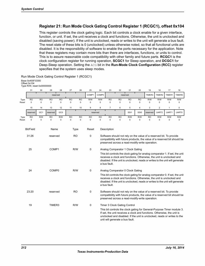
Register 21: RunMode Clock Gating Control Register 1 (RCGC1), offset 0x104This register controls the clock gating logic. Each bit controls a clock enable for a given interface,function, or unit. If set, the unit receives a clock and functions. Otherwise, the unit is unclocked anddisabled (saving power). If the unit is unclocked, reads or writes to the unit will generate a bus fault.The reset state of these bits is 0 (unclocked) unless otherwise noted, so that all functional units aredisabled. It is the responsibility of software to enable the ports necessary for the application. Notethat these registers may contain more bits than there are interfaces, functions, or units to control.This is to assure reasonable code compatibility with other family and future parts. RCGC1 is theclock configuration register for running operation, SCGC1 for Sleep operation, and DCGC1 forDeep-Sleep operation. Setting the ACG bit in the Run-Mode Clock Configuration (RCC) registerspecifies that the system uses sleep modes.
Run Mode Clock Gating Control Register 1 (RCGC1)Base 0x400F.E000Offset 0x104Type R/W, reset 0x00000000
16171819202122232425262728293031
TIMER0TIMER1TIMER2TIMER3reservedCOMP0COMP1reserved
R/WR/WR/WR/WROROROROR/WR/WROROROROROROType0000000000000000Reset
0123456789101112131415
UART0UART1UART2reservedSSI0SSI1reservedI2C0reservedI2C1reserved
R/WR/WR/WROR/WR/WROROROROROROR/WROR/WROType0000000000000000Reset
DescriptionResetTypeNameBit/Field
Software should not rely on the value of a reserved bit. To providecompatibility with future products, the value of a reserved bit should bepreserved across a read-modify-write operation.
0ROreserved31:26
Analog Comparator 1 Clock GatingThis bit controls the clock gating for analog comparator 1. If set, the unitreceives a clock and functions. Otherwise, the unit is unclocked anddisabled. If the unit is unclocked, reads or writes to the unit will generatea bus fault.
0R/WCOMP125
Analog Comparator 0 Clock GatingThis bit controls the clock gating for analog comparator 0. If set, the unitreceives a clock and functions. Otherwise, the unit is unclocked anddisabled. If the unit is unclocked, reads or writes to the unit will generatea bus fault.
0R/WCOMP024
Software should not rely on the value of a reserved bit. To providecompatibility with future products, the value of a reserved bit should bepreserved across a read-modify-write operation.
0ROreserved23:20
Timer 3 Clock Gating ControlThis bit controls the clock gating for General-Purpose Timer module 3.If set, the unit receives a clock and functions. Otherwise, the unit isunclocked and disabled. If the unit is unclocked, reads or writes to theunit will generate a bus fault.
0R/WTIMER319
July 16, 2014212Texas Instruments-Production Data
System Control
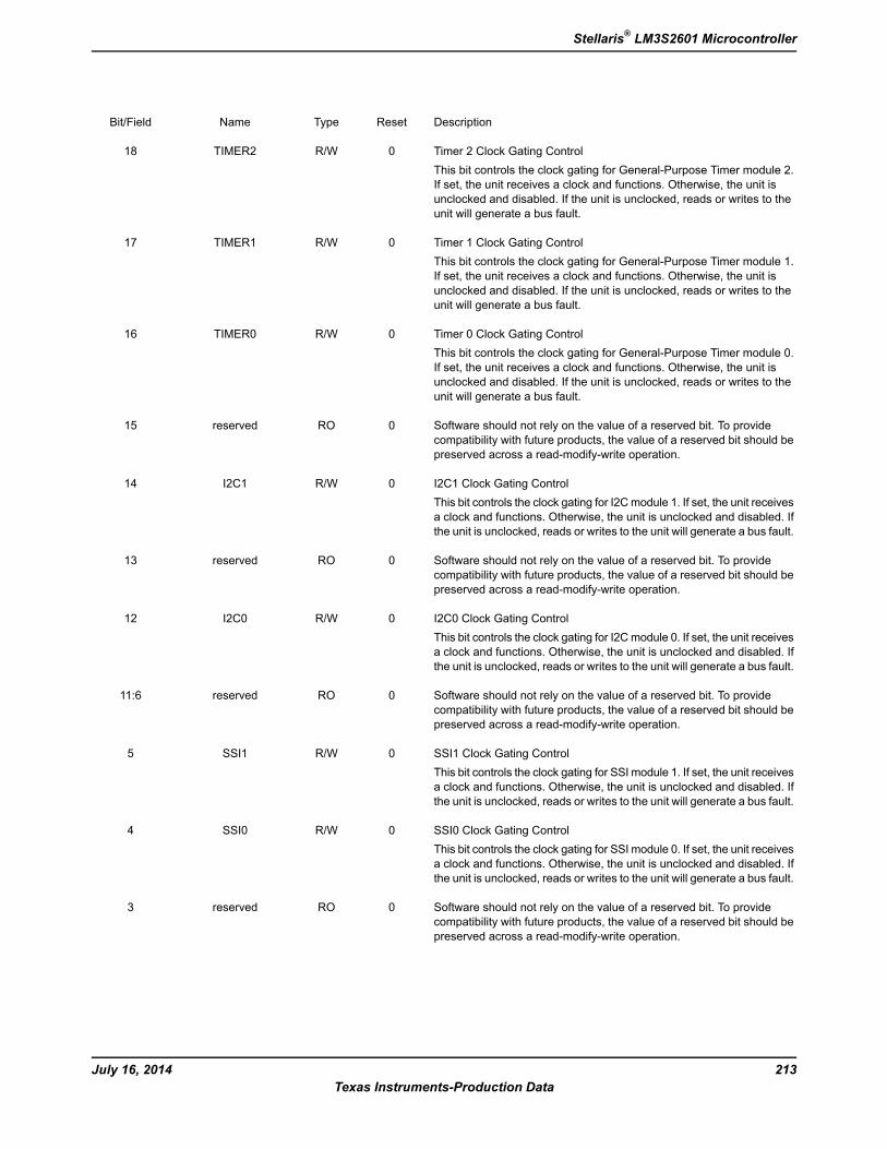
DescriptionResetTypeNameBit/Field
Timer 2 Clock Gating ControlThis bit controls the clock gating for General-Purpose Timer module 2.If set, the unit receives a clock and functions. Otherwise, the unit isunclocked and disabled. If the unit is unclocked, reads or writes to theunit will generate a bus fault.
0R/WTIMER218
Timer 1 Clock Gating ControlThis bit controls the clock gating for General-Purpose Timer module 1.If set, the unit receives a clock and functions. Otherwise, the unit isunclocked and disabled. If the unit is unclocked, reads or writes to theunit will generate a bus fault.
0R/WTIMER117
Timer 0 Clock Gating ControlThis bit controls the clock gating for General-Purpose Timer module 0.If set, the unit receives a clock and functions. Otherwise, the unit isunclocked and disabled. If the unit is unclocked, reads or writes to theunit will generate a bus fault.
0R/WTIMER016
Software should not rely on the value of a reserved bit. To providecompatibility with future products, the value of a reserved bit should bepreserved across a read-modify-write operation.
0ROreserved15
I2C1 Clock Gating ControlThis bit controls the clock gating for I2Cmodule 1. If set, the unit receivesa clock and functions. Otherwise, the unit is unclocked and disabled. Ifthe unit is unclocked, reads or writes to the unit will generate a bus fault.
0R/WI2C114
Software should not rely on the value of a reserved bit. To providecompatibility with future products, the value of a reserved bit should bepreserved across a read-modify-write operation.
0ROreserved13
I2C0 Clock Gating ControlThis bit controls the clock gating for I2Cmodule 0. If set, the unit receivesa clock and functions. Otherwise, the unit is unclocked and disabled. Ifthe unit is unclocked, reads or writes to the unit will generate a bus fault.
0R/WI2C012
Software should not rely on the value of a reserved bit. To providecompatibility with future products, the value of a reserved bit should bepreserved across a read-modify-write operation.
0ROreserved11:6
SSI1 Clock Gating ControlThis bit controls the clock gating for SSI module 1. If set, the unit receivesa clock and functions. Otherwise, the unit is unclocked and disabled. Ifthe unit is unclocked, reads or writes to the unit will generate a bus fault.
0R/WSSI15
SSI0 Clock Gating ControlThis bit controls the clock gating for SSI module 0. If set, the unit receivesa clock and functions. Otherwise, the unit is unclocked and disabled. Ifthe unit is unclocked, reads or writes to the unit will generate a bus fault.
0R/WSSI04
Software should not rely on the value of a reserved bit. To providecompatibility with future products, the value of a reserved bit should bepreserved across a read-modify-write operation.
0ROreserved3
213July 16, 2014Texas Instruments-Production Data
Stellaris® LM3S2601 Microcontroller

DescriptionResetTypeNameBit/Field
UART2 Clock Gating ControlThis bit controls the clock gating for UART module 2. If set, the unitreceives a clock and functions. Otherwise, the unit is unclocked anddisabled. If the unit is unclocked, reads or writes to the unit will generatea bus fault.
0R/WUART22
UART1 Clock Gating ControlThis bit controls the clock gating for UART module 1. If set, the unitreceives a clock and functions. Otherwise, the unit is unclocked anddisabled. If the unit is unclocked, reads or writes to the unit will generatea bus fault.
0R/WUART11
UART0 Clock Gating ControlThis bit controls the clock gating for UART module 0. If set, the unitreceives a clock and functions. Otherwise, the unit is unclocked anddisabled. If the unit is unclocked, reads or writes to the unit will generatea bus fault.
0R/WUART00
July 16, 2014214Texas Instruments-Production Data
System Control
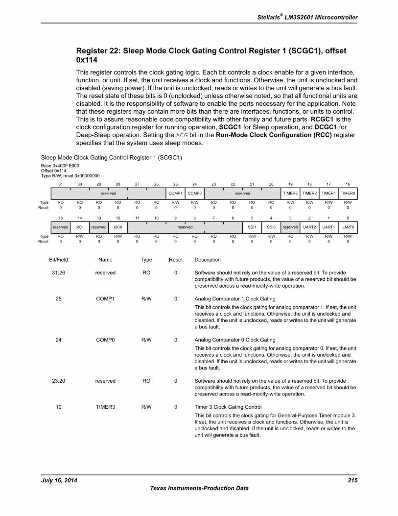
Register 22: Sleep Mode Clock Gating Control Register 1 (SCGC1), offset0x114This register controls the clock gating logic. Each bit controls a clock enable for a given interface,function, or unit. If set, the unit receives a clock and functions. Otherwise, the unit is unclocked anddisabled (saving power). If the unit is unclocked, reads or writes to the unit will generate a bus fault.The reset state of these bits is 0 (unclocked) unless otherwise noted, so that all functional units aredisabled. It is the responsibility of software to enable the ports necessary for the application. Notethat these registers may contain more bits than there are interfaces, functions, or units to control.This is to assure reasonable code compatibility with other family and future parts. RCGC1 is theclock configuration register for running operation, SCGC1 for Sleep operation, and DCGC1 forDeep-Sleep operation. Setting the ACG bit in the Run-Mode Clock Configuration (RCC) registerspecifies that the system uses sleep modes.
Sleep Mode Clock Gating Control Register 1 (SCGC1)Base 0x400F.E000Offset 0x114Type R/W, reset 0x00000000
16171819202122232425262728293031
TIMER0TIMER1TIMER2TIMER3reservedCOMP0COMP1reserved
R/WR/WR/WR/WROROROROR/WR/WROROROROROROType0000000000000000Reset
0123456789101112131415
UART0UART1UART2reservedSSI0SSI1reservedI2C0reservedI2C1reserved
R/WR/WR/WROR/WR/WROROROROROROR/WROR/WROType0000000000000000Reset
DescriptionResetTypeNameBit/Field
Software should not rely on the value of a reserved bit. To providecompatibility with future products, the value of a reserved bit should bepreserved across a read-modify-write operation.
0ROreserved31:26
Analog Comparator 1 Clock GatingThis bit controls the clock gating for analog comparator 1. If set, the unitreceives a clock and functions. Otherwise, the unit is unclocked anddisabled. If the unit is unclocked, reads or writes to the unit will generatea bus fault.
0R/WCOMP125
Analog Comparator 0 Clock GatingThis bit controls the clock gating for analog comparator 0. If set, the unitreceives a clock and functions. Otherwise, the unit is unclocked anddisabled. If the unit is unclocked, reads or writes to the unit will generatea bus fault.
0R/WCOMP024
Software should not rely on the value of a reserved bit. To providecompatibility with future products, the value of a reserved bit should bepreserved across a read-modify-write operation.
0ROreserved23:20
Timer 3 Clock Gating ControlThis bit controls the clock gating for General-Purpose Timer module 3.If set, the unit receives a clock and functions. Otherwise, the unit isunclocked and disabled. If the unit is unclocked, reads or writes to theunit will generate a bus fault.
0R/WTIMER319
215July 16, 2014Texas Instruments-Production Data
Stellaris® LM3S2601 Microcontroller
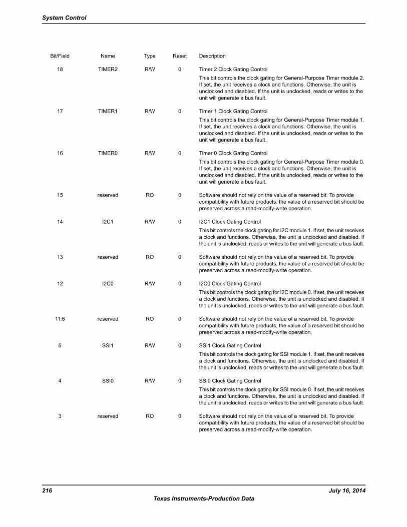
DescriptionResetTypeNameBit/Field
Timer 2 Clock Gating ControlThis bit controls the clock gating for General-Purpose Timer module 2.If set, the unit receives a clock and functions. Otherwise, the unit isunclocked and disabled. If the unit is unclocked, reads or writes to theunit will generate a bus fault.
0R/WTIMER218
Timer 1 Clock Gating ControlThis bit controls the clock gating for General-Purpose Timer module 1.If set, the unit receives a clock and functions. Otherwise, the unit isunclocked and disabled. If the unit is unclocked, reads or writes to theunit will generate a bus fault.
0R/WTIMER117
Timer 0 Clock Gating ControlThis bit controls the clock gating for General-Purpose Timer module 0.If set, the unit receives a clock and functions. Otherwise, the unit isunclocked and disabled. If the unit is unclocked, reads or writes to theunit will generate a bus fault.
0R/WTIMER016
Software should not rely on the value of a reserved bit. To providecompatibility with future products, the value of a reserved bit should bepreserved across a read-modify-write operation.
0ROreserved15
I2C1 Clock Gating ControlThis bit controls the clock gating for I2Cmodule 1. If set, the unit receivesa clock and functions. Otherwise, the unit is unclocked and disabled. Ifthe unit is unclocked, reads or writes to the unit will generate a bus fault.
0R/WI2C114
Software should not rely on the value of a reserved bit. To providecompatibility with future products, the value of a reserved bit should bepreserved across a read-modify-write operation.
0ROreserved13
I2C0 Clock Gating ControlThis bit controls the clock gating for I2Cmodule 0. If set, the unit receivesa clock and functions. Otherwise, the unit is unclocked and disabled. Ifthe unit is unclocked, reads or writes to the unit will generate a bus fault.
0R/WI2C012
Software should not rely on the value of a reserved bit. To providecompatibility with future products, the value of a reserved bit should bepreserved across a read-modify-write operation.
0ROreserved11:6
SSI1 Clock Gating ControlThis bit controls the clock gating for SSI module 1. If set, the unit receivesa clock and functions. Otherwise, the unit is unclocked and disabled. Ifthe unit is unclocked, reads or writes to the unit will generate a bus fault.
0R/WSSI15
SSI0 Clock Gating ControlThis bit controls the clock gating for SSI module 0. If set, the unit receivesa clock and functions. Otherwise, the unit is unclocked and disabled. Ifthe unit is unclocked, reads or writes to the unit will generate a bus fault.
0R/WSSI04
Software should not rely on the value of a reserved bit. To providecompatibility with future products, the value of a reserved bit should bepreserved across a read-modify-write operation.
0ROreserved3
July 16, 2014216Texas Instruments-Production Data
System Control
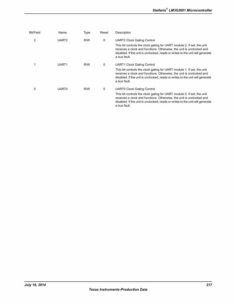
DescriptionResetTypeNameBit/Field
UART2 Clock Gating ControlThis bit controls the clock gating for UART module 2. If set, the unitreceives a clock and functions. Otherwise, the unit is unclocked anddisabled. If the unit is unclocked, reads or writes to the unit will generatea bus fault.
0R/WUART22
UART1 Clock Gating ControlThis bit controls the clock gating for UART module 1. If set, the unitreceives a clock and functions. Otherwise, the unit is unclocked anddisabled. If the unit is unclocked, reads or writes to the unit will generatea bus fault.
0R/WUART11
UART0 Clock Gating ControlThis bit controls the clock gating for UART module 0. If set, the unitreceives a clock and functions. Otherwise, the unit is unclocked anddisabled. If the unit is unclocked, reads or writes to the unit will generatea bus fault.
0R/WUART00
217July 16, 2014Texas Instruments-Production Data
Stellaris® LM3S2601 Microcontroller
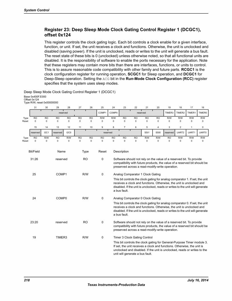
Register 23: Deep Sleep Mode Clock Gating Control Register 1 (DCGC1),offset 0x124This register controls the clock gating logic. Each bit controls a clock enable for a given interface,function, or unit. If set, the unit receives a clock and functions. Otherwise, the unit is unclocked anddisabled (saving power). If the unit is unclocked, reads or writes to the unit will generate a bus fault.The reset state of these bits is 0 (unclocked) unless otherwise noted, so that all functional units aredisabled. It is the responsibility of software to enable the ports necessary for the application. Notethat these registers may contain more bits than there are interfaces, functions, or units to control.This is to assure reasonable code compatibility with other family and future parts. RCGC1 is theclock configuration register for running operation, SCGC1 for Sleep operation, and DCGC1 forDeep-Sleep operation. Setting the ACG bit in the Run-Mode Clock Configuration (RCC) registerspecifies that the system uses sleep modes.
Deep Sleep Mode Clock Gating Control Register 1 (DCGC1)Base 0x400F.E000Offset 0x124Type R/W, reset 0x00000000
16171819202122232425262728293031
TIMER0TIMER1TIMER2TIMER3reservedCOMP0COMP1reserved
R/WR/WR/WR/WROROROROR/WR/WROROROROROROType0000000000000000Reset
0123456789101112131415
UART0UART1UART2reservedSSI0SSI1reservedI2C0reservedI2C1reserved
R/WR/WR/WROR/WR/WROROROROROROR/WROR/WROType0000000000000000Reset
DescriptionResetTypeNameBit/Field
Software should not rely on the value of a reserved bit. To providecompatibility with future products, the value of a reserved bit should bepreserved across a read-modify-write operation.
0ROreserved31:26
Analog Comparator 1 Clock GatingThis bit controls the clock gating for analog comparator 1. If set, the unitreceives a clock and functions. Otherwise, the unit is unclocked anddisabled. If the unit is unclocked, reads or writes to the unit will generatea bus fault.
0R/WCOMP125
Analog Comparator 0 Clock GatingThis bit controls the clock gating for analog comparator 0. If set, the unitreceives a clock and functions. Otherwise, the unit is unclocked anddisabled. If the unit is unclocked, reads or writes to the unit will generatea bus fault.
0R/WCOMP024
Software should not rely on the value of a reserved bit. To providecompatibility with future products, the value of a reserved bit should bepreserved across a read-modify-write operation.
0ROreserved23:20
Timer 3 Clock Gating ControlThis bit controls the clock gating for General-Purpose Timer module 3.If set, the unit receives a clock and functions. Otherwise, the unit isunclocked and disabled. If the unit is unclocked, reads or writes to theunit will generate a bus fault.
0R/WTIMER319
July 16, 2014218Texas Instruments-Production Data
System Control

DescriptionResetTypeNameBit/Field
Timer 2 Clock Gating ControlThis bit controls the clock gating for General-Purpose Timer module 2.If set, the unit receives a clock and functions. Otherwise, the unit isunclocked and disabled. If the unit is unclocked, reads or writes to theunit will generate a bus fault.
0R/WTIMER218
Timer 1 Clock Gating ControlThis bit controls the clock gating for General-Purpose Timer module 1.If set, the unit receives a clock and functions. Otherwise, the unit isunclocked and disabled. If the unit is unclocked, reads or writes to theunit will generate a bus fault.
0R/WTIMER117
Timer 0 Clock Gating ControlThis bit controls the clock gating for General-Purpose Timer module 0.If set, the unit receives a clock and functions. Otherwise, the unit isunclocked and disabled. If the unit is unclocked, reads or writes to theunit will generate a bus fault.
0R/WTIMER016
Software should not rely on the value of a reserved bit. To providecompatibility with future products, the value of a reserved bit should bepreserved across a read-modify-write operation.
0ROreserved15
I2C1 Clock Gating ControlThis bit controls the clock gating for I2Cmodule 1. If set, the unit receivesa clock and functions. Otherwise, the unit is unclocked and disabled. Ifthe unit is unclocked, reads or writes to the unit will generate a bus fault.
0R/WI2C114
Software should not rely on the value of a reserved bit. To providecompatibility with future products, the value of a reserved bit should bepreserved across a read-modify-write operation.
0ROreserved13
I2C0 Clock Gating ControlThis bit controls the clock gating for I2Cmodule 0. If set, the unit receivesa clock and functions. Otherwise, the unit is unclocked and disabled. Ifthe unit is unclocked, reads or writes to the unit will generate a bus fault.
0R/WI2C012
Software should not rely on the value of a reserved bit. To providecompatibility with future products, the value of a reserved bit should bepreserved across a read-modify-write operation.
0ROreserved11:6
SSI1 Clock Gating ControlThis bit controls the clock gating for SSI module 1. If set, the unit receivesa clock and functions. Otherwise, the unit is unclocked and disabled. Ifthe unit is unclocked, reads or writes to the unit will generate a bus fault.
0R/WSSI15
SSI0 Clock Gating ControlThis bit controls the clock gating for SSI module 0. If set, the unit receivesa clock and functions. Otherwise, the unit is unclocked and disabled. Ifthe unit is unclocked, reads or writes to the unit will generate a bus fault.
0R/WSSI04
Software should not rely on the value of a reserved bit. To providecompatibility with future products, the value of a reserved bit should bepreserved across a read-modify-write operation.
0ROreserved3
219July 16, 2014Texas Instruments-Production Data
Stellaris® LM3S2601 Microcontroller
DescriptionResetTypeNameBit/Field
UART2 Clock Gating ControlThis bit controls the clock gating for UART module 2. If set, the unitreceives a clock and functions. Otherwise, the unit is unclocked anddisabled. If the unit is unclocked, reads or writes to the unit will generatea bus fault.
0R/WUART22
UART1 Clock Gating ControlThis bit controls the clock gating for UART module 1. If set, the unitreceives a clock and functions. Otherwise, the unit is unclocked anddisabled. If the unit is unclocked, reads or writes to the unit will generatea bus fault.
0R/WUART11
UART0 Clock Gating ControlThis bit controls the clock gating for UART module 0. If set, the unitreceives a clock and functions. Otherwise, the unit is unclocked anddisabled. If the unit is unclocked, reads or writes to the unit will generatea bus fault.
0R/WUART00
July 16, 2014220Texas Instruments-Production Data
System Control
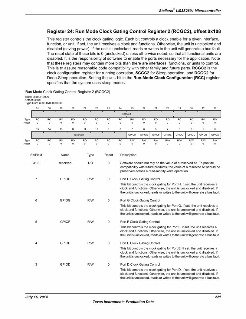
Register 24: RunMode Clock Gating Control Register 2 (RCGC2), offset 0x108This register controls the clock gating logic. Each bit controls a clock enable for a given interface,function, or unit. If set, the unit receives a clock and functions. Otherwise, the unit is unclocked anddisabled (saving power). If the unit is unclocked, reads or writes to the unit will generate a bus fault.The reset state of these bits is 0 (unclocked) unless otherwise noted, so that all functional units aredisabled. It is the responsibility of software to enable the ports necessary for the application. Notethat these registers may contain more bits than there are interfaces, functions, or units to control.This is to assure reasonable code compatibility with other family and future parts. RCGC2 is theclock configuration register for running operation, SCGC2 for Sleep operation, and DCGC2 forDeep-Sleep operation. Setting the ACG bit in the Run-Mode Clock Configuration (RCC) registerspecifies that the system uses sleep modes.
Run Mode Clock Gating Control Register 2 (RCGC2)Base 0x400F.E000Offset 0x108Type R/W, reset 0x00000000
16171819202122232425262728293031
reserved
ROROROROROROROROROROROROROROROROType0000000000000000Reset
0123456789101112131415
GPIOAGPIOBGPIOCGPIODGPIOEGPIOFGPIOGGPIOHreserved
R/WR/WR/WR/WR/WR/WR/WR/WROROROROROROROROType0000000000000000Reset
DescriptionResetTypeNameBit/Field
Software should not rely on the value of a reserved bit. To providecompatibility with future products, the value of a reserved bit should bepreserved across a read-modify-write operation.
0ROreserved31:8
Port H Clock Gating ControlThis bit controls the clock gating for Port H. If set, the unit receives aclock and functions. Otherwise, the unit is unclocked and disabled. Ifthe unit is unclocked, reads or writes to the unit will generate a bus fault.
0R/WGPIOH7
Port G Clock Gating ControlThis bit controls the clock gating for Port G. If set, the unit receives aclock and functions. Otherwise, the unit is unclocked and disabled. Ifthe unit is unclocked, reads or writes to the unit will generate a bus fault.
0R/WGPIOG6
Port F Clock Gating ControlThis bit controls the clock gating for Port F. If set, the unit receives aclock and functions. Otherwise, the unit is unclocked and disabled. Ifthe unit is unclocked, reads or writes to the unit will generate a bus fault.
0R/WGPIOF5
Port E Clock Gating ControlThis bit controls the clock gating for Port E. If set, the unit receives aclock and functions. Otherwise, the unit is unclocked and disabled. Ifthe unit is unclocked, reads or writes to the unit will generate a bus fault.
0R/WGPIOE4
Port D Clock Gating ControlThis bit controls the clock gating for Port D. If set, the unit receives aclock and functions. Otherwise, the unit is unclocked and disabled. Ifthe unit is unclocked, reads or writes to the unit will generate a bus fault.
0R/WGPIOD3
221July 16, 2014Texas Instruments-Production Data
Stellaris® LM3S2601 Microcontroller
DescriptionResetTypeNameBit/Field
Port C Clock Gating ControlThis bit controls the clock gating for Port C. If set, the unit receives aclock and functions. Otherwise, the unit is unclocked and disabled. Ifthe unit is unclocked, reads or writes to the unit will generate a bus fault.
0R/WGPIOC2
Port B Clock Gating ControlThis bit controls the clock gating for Port B. If set, the unit receives aclock and functions. Otherwise, the unit is unclocked and disabled. Ifthe unit is unclocked, reads or writes to the unit will generate a bus fault.
0R/WGPIOB1
Port A Clock Gating ControlThis bit controls the clock gating for Port A. If set, the unit receives aclock and functions. Otherwise, the unit is unclocked and disabled. Ifthe unit is unclocked, reads or writes to the unit will generate a bus fault.
0R/WGPIOA0
July 16, 2014222Texas Instruments-Production Data
System Control

Register 25: Sleep Mode Clock Gating Control Register 2 (SCGC2), offset0x118This register controls the clock gating logic. Each bit controls a clock enable for a given interface,function, or unit. If set, the unit receives a clock and functions. Otherwise, the unit is unclocked anddisabled (saving power). If the unit is unclocked, reads or writes to the unit will generate a bus fault.The reset state of these bits is 0 (unclocked) unless otherwise noted, so that all functional units aredisabled. It is the responsibility of software to enable the ports necessary for the application. Notethat these registers may contain more bits than there are interfaces, functions, or units to control.This is to assure reasonable code compatibility with other family and future parts. RCGC2 is theclock configuration register for running operation, SCGC2 for Sleep operation, and DCGC2 forDeep-Sleep operation. Setting the ACG bit in the Run-Mode Clock Configuration (RCC) registerspecifies that the system uses sleep modes.
Sleep Mode Clock Gating Control Register 2 (SCGC2)Base 0x400F.E000Offset 0x118Type R/W, reset 0x00000000
16171819202122232425262728293031
reserved
ROROROROROROROROROROROROROROROROType0000000000000000Reset
0123456789101112131415
GPIOAGPIOBGPIOCGPIODGPIOEGPIOFGPIOGGPIOHreserved
R/WR/WR/WR/WR/WR/WR/WR/WROROROROROROROROType0000000000000000Reset
DescriptionResetTypeNameBit/Field
Software should not rely on the value of a reserved bit. To providecompatibility with future products, the value of a reserved bit should bepreserved across a read-modify-write operation.
0ROreserved31:8
Port H Clock Gating ControlThis bit controls the clock gating for Port H. If set, the unit receives aclock and functions. Otherwise, the unit is unclocked and disabled. Ifthe unit is unclocked, reads or writes to the unit will generate a bus fault.
0R/WGPIOH7
Port G Clock Gating ControlThis bit controls the clock gating for Port G. If set, the unit receives aclock and functions. Otherwise, the unit is unclocked and disabled. Ifthe unit is unclocked, reads or writes to the unit will generate a bus fault.
0R/WGPIOG6
Port F Clock Gating ControlThis bit controls the clock gating for Port F. If set, the unit receives aclock and functions. Otherwise, the unit is unclocked and disabled. Ifthe unit is unclocked, reads or writes to the unit will generate a bus fault.
0R/WGPIOF5
Port E Clock Gating ControlThis bit controls the clock gating for Port E. If set, the unit receives aclock and functions. Otherwise, the unit is unclocked and disabled. Ifthe unit is unclocked, reads or writes to the unit will generate a bus fault.
0R/WGPIOE4
223July 16, 2014Texas Instruments-Production Data
Stellaris® LM3S2601 Microcontroller
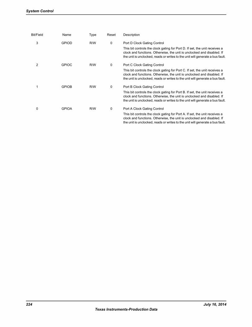
DescriptionResetTypeNameBit/Field
Port D Clock Gating ControlThis bit controls the clock gating for Port D. If set, the unit receives aclock and functions. Otherwise, the unit is unclocked and disabled. Ifthe unit is unclocked, reads or writes to the unit will generate a bus fault.
0R/WGPIOD3
Port C Clock Gating ControlThis bit controls the clock gating for Port C. If set, the unit receives aclock and functions. Otherwise, the unit is unclocked and disabled. Ifthe unit is unclocked, reads or writes to the unit will generate a bus fault.
0R/WGPIOC2
Port B Clock Gating ControlThis bit controls the clock gating for Port B. If set, the unit receives aclock and functions. Otherwise, the unit is unclocked and disabled. Ifthe unit is unclocked, reads or writes to the unit will generate a bus fault.
0R/WGPIOB1
Port A Clock Gating ControlThis bit controls the clock gating for Port A. If set, the unit receives aclock and functions. Otherwise, the unit is unclocked and disabled. Ifthe unit is unclocked, reads or writes to the unit will generate a bus fault.
0R/WGPIOA0
July 16, 2014224Texas Instruments-Production Data
System Control
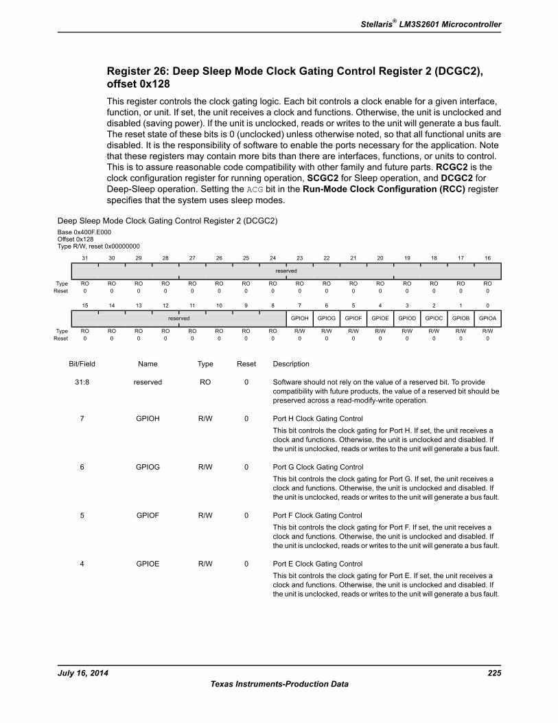
Register 26: Deep Sleep Mode Clock Gating Control Register 2 (DCGC2),offset 0x128This register controls the clock gating logic. Each bit controls a clock enable for a given interface,function, or unit. If set, the unit receives a clock and functions. Otherwise, the unit is unclocked anddisabled (saving power). If the unit is unclocked, reads or writes to the unit will generate a bus fault.The reset state of these bits is 0 (unclocked) unless otherwise noted, so that all functional units aredisabled. It is the responsibility of software to enable the ports necessary for the application. Notethat these registers may contain more bits than there are interfaces, functions, or units to control.This is to assure reasonable code compatibility with other family and future parts. RCGC2 is theclock configuration register for running operation, SCGC2 for Sleep operation, and DCGC2 forDeep-Sleep operation. Setting the ACG bit in the Run-Mode Clock Configuration (RCC) registerspecifies that the system uses sleep modes.
Deep Sleep Mode Clock Gating Control Register 2 (DCGC2)Base 0x400F.E000Offset 0x128Type R/W, reset 0x00000000
16171819202122232425262728293031
reserved
ROROROROROROROROROROROROROROROROType0000000000000000Reset
0123456789101112131415
GPIOAGPIOBGPIOCGPIODGPIOEGPIOFGPIOGGPIOHreserved
R/WR/WR/WR/WR/WR/WR/WR/WROROROROROROROROType0000000000000000Reset
DescriptionResetTypeNameBit/Field
Software should not rely on the value of a reserved bit. To providecompatibility with future products, the value of a reserved bit should bepreserved across a read-modify-write operation.
0ROreserved31:8
Port H Clock Gating ControlThis bit controls the clock gating for Port H. If set, the unit receives aclock and functions. Otherwise, the unit is unclocked and disabled. Ifthe unit is unclocked, reads or writes to the unit will generate a bus fault.
0R/WGPIOH7
Port G Clock Gating ControlThis bit controls the clock gating for Port G. If set, the unit receives aclock and functions. Otherwise, the unit is unclocked and disabled. Ifthe unit is unclocked, reads or writes to the unit will generate a bus fault.
0R/WGPIOG6
Port F Clock Gating ControlThis bit controls the clock gating for Port F. If set, the unit receives aclock and functions. Otherwise, the unit is unclocked and disabled. Ifthe unit is unclocked, reads or writes to the unit will generate a bus fault.
0R/WGPIOF5
Port E Clock Gating ControlThis bit controls the clock gating for Port E. If set, the unit receives aclock and functions. Otherwise, the unit is unclocked and disabled. Ifthe unit is unclocked, reads or writes to the unit will generate a bus fault.
0R/WGPIOE4
225July 16, 2014Texas Instruments-Production Data
Stellaris® LM3S2601 Microcontroller

DescriptionResetTypeNameBit/Field
Port D Clock Gating ControlThis bit controls the clock gating for Port D. If set, the unit receives aclock and functions. Otherwise, the unit is unclocked and disabled. Ifthe unit is unclocked, reads or writes to the unit will generate a bus fault.
0R/WGPIOD3
Port C Clock Gating ControlThis bit controls the clock gating for Port C. If set, the unit receives aclock and functions. Otherwise, the unit is unclocked and disabled. Ifthe unit is unclocked, reads or writes to the unit will generate a bus fault.
0R/WGPIOC2
Port B Clock Gating ControlThis bit controls the clock gating for Port B. If set, the unit receives aclock and functions. Otherwise, the unit is unclocked and disabled. Ifthe unit is unclocked, reads or writes to the unit will generate a bus fault.
0R/WGPIOB1
Port A Clock Gating ControlThis bit controls the clock gating for Port A. If set, the unit receives aclock and functions. Otherwise, the unit is unclocked and disabled. Ifthe unit is unclocked, reads or writes to the unit will generate a bus fault.
0R/WGPIOA0
July 16, 2014226Texas Instruments-Production Data
System Control
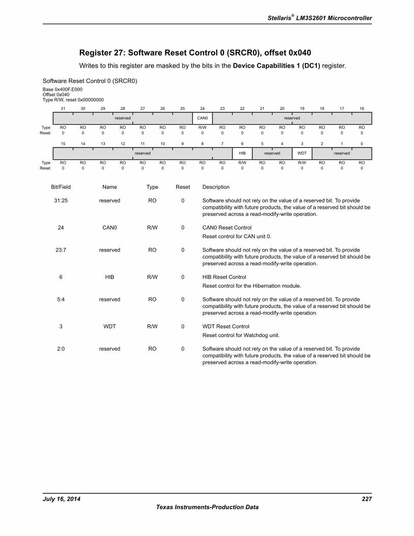
Register 27: Software Reset Control 0 (SRCR0), offset 0x040Writes to this register are masked by the bits in the Device Capabilities 1 (DC1) register.
Software Reset Control 0 (SRCR0)Base 0x400F.E000Offset 0x040Type R/W, reset 0x00000000
16171819202122232425262728293031
reservedCAN0reserved
ROROROROROROROROR/WROROROROROROROType0000000000000000Reset
0123456789101112131415
reservedWDTreservedHIBreserved
ROROROR/WROROR/WROROROROROROROROROType0000000000000000Reset
DescriptionResetTypeNameBit/Field
Software should not rely on the value of a reserved bit. To providecompatibility with future products, the value of a reserved bit should bepreserved across a read-modify-write operation.
0ROreserved31:25
CAN0 Reset ControlReset control for CAN unit 0.
0R/WCAN024
Software should not rely on the value of a reserved bit. To providecompatibility with future products, the value of a reserved bit should bepreserved across a read-modify-write operation.
0ROreserved23:7
HIB Reset ControlReset control for the Hibernation module.
0R/WHIB6
Software should not rely on the value of a reserved bit. To providecompatibility with future products, the value of a reserved bit should bepreserved across a read-modify-write operation.
0ROreserved5:4
WDT Reset ControlReset control for Watchdog unit.
0R/WWDT3
Software should not rely on the value of a reserved bit. To providecompatibility with future products, the value of a reserved bit should bepreserved across a read-modify-write operation.
0ROreserved2:0
227July 16, 2014Texas Instruments-Production Data
Stellaris® LM3S2601 Microcontroller
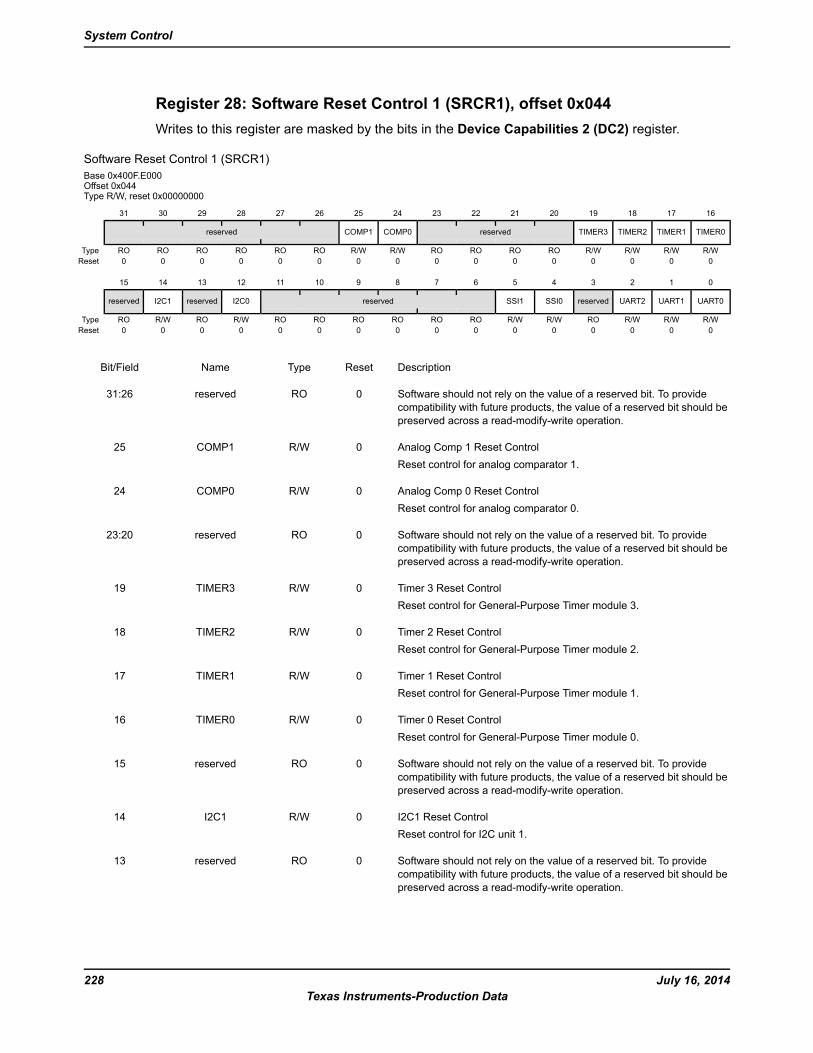
Register 28: Software Reset Control 1 (SRCR1), offset 0x044Writes to this register are masked by the bits in the Device Capabilities 2 (DC2) register.
Software Reset Control 1 (SRCR1)Base 0x400F.E000Offset 0x044Type R/W, reset 0x00000000
16171819202122232425262728293031
TIMER0TIMER1TIMER2TIMER3reservedCOMP0COMP1reserved
R/WR/WR/WR/WROROROROR/WR/WROROROROROROType0000000000000000Reset
0123456789101112131415
UART0UART1UART2reservedSSI0SSI1reservedI2C0reservedI2C1reserved
R/WR/WR/WROR/WR/WROROROROROROR/WROR/WROType0000000000000000Reset
DescriptionResetTypeNameBit/Field
Software should not rely on the value of a reserved bit. To providecompatibility with future products, the value of a reserved bit should bepreserved across a read-modify-write operation.
0ROreserved31:26
Analog Comp 1 Reset ControlReset control for analog comparator 1.
0R/WCOMP125
Analog Comp 0 Reset ControlReset control for analog comparator 0.
0R/WCOMP024
Software should not rely on the value of a reserved bit. To providecompatibility with future products, the value of a reserved bit should bepreserved across a read-modify-write operation.
0ROreserved23:20
Timer 3 Reset ControlReset control for General-Purpose Timer module 3.
0R/WTIMER319
Timer 2 Reset ControlReset control for General-Purpose Timer module 2.
0R/WTIMER218
Timer 1 Reset ControlReset control for General-Purpose Timer module 1.
0R/WTIMER117
Timer 0 Reset ControlReset control for General-Purpose Timer module 0.
0R/WTIMER016
Software should not rely on the value of a reserved bit. To providecompatibility with future products, the value of a reserved bit should bepreserved across a read-modify-write operation.
0ROreserved15
I2C1 Reset ControlReset control for I2C unit 1.
0R/WI2C114
Software should not rely on the value of a reserved bit. To providecompatibility with future products, the value of a reserved bit should bepreserved across a read-modify-write operation.
0ROreserved13
July 16, 2014228Texas Instruments-Production Data
System Control
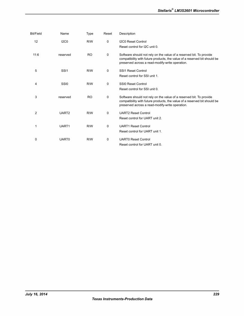
DescriptionResetTypeNameBit/Field
I2C0 Reset ControlReset control for I2C unit 0.
0R/WI2C012
Software should not rely on the value of a reserved bit. To providecompatibility with future products, the value of a reserved bit should bepreserved across a read-modify-write operation.
0ROreserved11:6
SSI1 Reset ControlReset control for SSI unit 1.
0R/WSSI15
SSI0 Reset ControlReset control for SSI unit 0.
0R/WSSI04
Software should not rely on the value of a reserved bit. To providecompatibility with future products, the value of a reserved bit should bepreserved across a read-modify-write operation.
0ROreserved3
UART2 Reset ControlReset control for UART unit 2.
0R/WUART22
UART1 Reset ControlReset control for UART unit 1.
0R/WUART11
UART0 Reset ControlReset control for UART unit 0.
0R/WUART00
229July 16, 2014Texas Instruments-Production Data
Stellaris® LM3S2601 Microcontroller
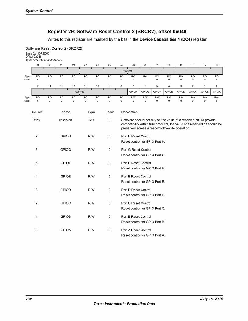
Register 29: Software Reset Control 2 (SRCR2), offset 0x048Writes to this register are masked by the bits in the Device Capabilities 4 (DC4) register.
Software Reset Control 2 (SRCR2)Base 0x400F.E000Offset 0x048Type R/W, reset 0x00000000
16171819202122232425262728293031
reserved
ROROROROROROROROROROROROROROROROType0000000000000000Reset
0123456789101112131415
GPIOAGPIOBGPIOCGPIODGPIOEGPIOFGPIOGGPIOHreserved
R/WR/WR/WR/WR/WR/WR/WR/WROROROROROROROROType0000000000000000Reset
DescriptionResetTypeNameBit/Field
Software should not rely on the value of a reserved bit. To providecompatibility with future products, the value of a reserved bit should bepreserved across a read-modify-write operation.
0ROreserved31:8
Port H Reset ControlReset control for GPIO Port H.
0R/WGPIOH7
Port G Reset ControlReset control for GPIO Port G.
0R/WGPIOG6
Port F Reset ControlReset control for GPIO Port F.
0R/WGPIOF5
Port E Reset ControlReset control for GPIO Port E.
0R/WGPIOE4
Port D Reset ControlReset control for GPIO Port D.
0R/WGPIOD3
Port C Reset ControlReset control for GPIO Port C.
0R/WGPIOC2
Port B Reset ControlReset control for GPIO Port B.
0R/WGPIOB1
Port A Reset ControlReset control for GPIO Port A.
0R/WGPIOA0
July 16, 2014230Texas Instruments-Production Data
System Control
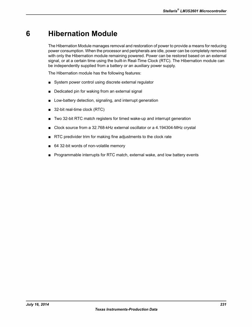
6 Hibernation ModuleThe Hibernation Module manages removal and restoration of power to provide a means for reducingpower consumption. When the processor and peripherals are idle, power can be completely removedwith only the Hibernation module remaining powered. Power can be restored based on an externalsignal, or at a certain time using the built-in Real-Time Clock (RTC). The Hibernation module canbe independently supplied from a battery or an auxiliary power supply.
The Hibernation module has the following features:
System power control using discrete external regulator
Dedicated pin for waking from an external signal
Low-battery detection, signaling, and interrupt generation
32-bit real-time clock (RTC)
Two 32-bit RTC match registers for timed wake-up and interrupt generation
Clock source from a 32.768-kHz external oscillator or a 4.194304-MHz crystal
RTC predivider trim for making fine adjustments to the clock rate
64 32-bit words of non-volatile memory
Programmable interrupts for RTC match, external wake, and low battery events
231July 16, 2014Texas Instruments-Production Data
Stellaris® LM3S2601 Microcontroller
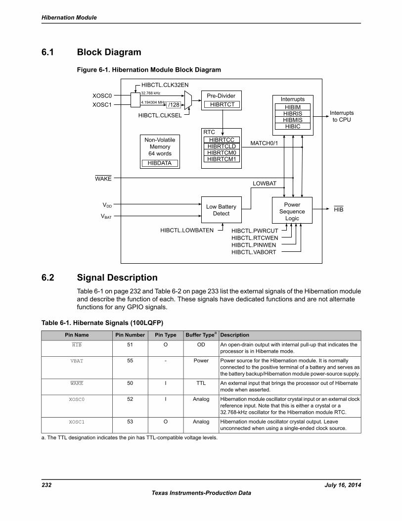
6.1 Block Diagram
Figure 6-1. Hibernation Module Block Diagram
HIBIMHIBRISHIBMISHIBIC
HIBRTCTPre-Divider
/128XOSC0XOSC1
HIBCTL.CLK32EN
HIBCTL.CLKSEL
HIBRTCCHIBRTCLDHIBRTCM0HIBRTCM1
RTC
Interrupts
PowerSequenceLogic
MATCH0/1
WAKE
Interruptsto CPU
Low BatteryDetect
LOWBAT
VDD
VBAT
HIB
HIBCTL.LOWBATEN HIBCTL.PWRCUT
HIBCTL.PINWENHIBCTL.RTCWEN
HIBCTL.VABORT
Non-VolatileMemory64 words
HIBDATA
32.768 kHz
4.194304 MHz
6.2 Signal DescriptionTable 6-1 on page 232 and Table 6-2 on page 233 list the external signals of the Hibernation moduleand describe the function of each. These signals have dedicated functions and are not alternatefunctions for any GPIO signals.
Table 6-1. Hibernate Signals (100LQFP)
DescriptionBuffer TypeaPin TypePin NumberPin Name
An open-drain output with internal pull-up that indicates theprocessor is in Hibernate mode.
ODO51HIB
Power source for the Hibernation module. It is normallyconnected to the positive terminal of a battery and serves asthe battery backup/Hibernation module power-source supply.
Power-55VBAT
An external input that brings the processor out of Hibernatemode when asserted.
TTLI50WAKE
Hibernation module oscillator crystal input or an external clockreference input. Note that this is either a crystal or a32.768-kHz oscillator for the Hibernation module RTC.
AnalogI52XOSC0
Hibernation module oscillator crystal output. Leaveunconnected when using a single-ended clock source.
AnalogO53XOSC1
a. The TTL designation indicates the pin has TTL-compatible voltage levels.
July 16, 2014232Texas Instruments-Production Data
Hibernation Module
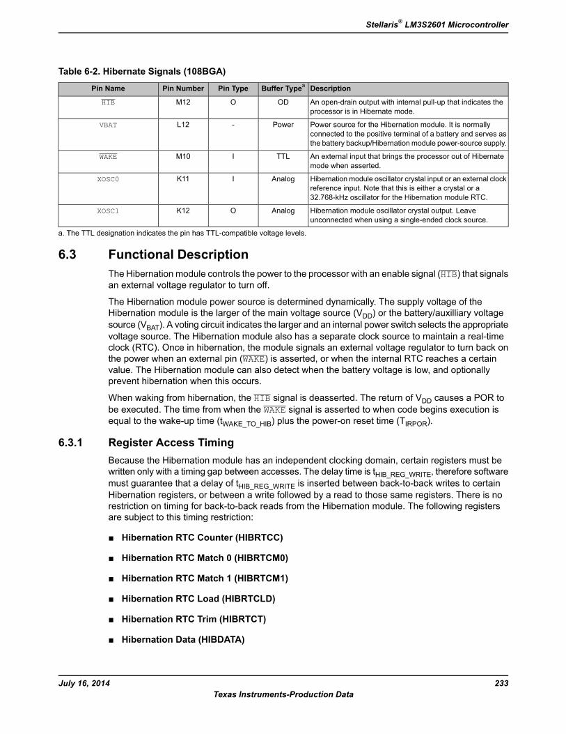
Table 6-2. Hibernate Signals (108BGA)
DescriptionBuffer TypeaPin TypePin NumberPin Name
An open-drain output with internal pull-up that indicates theprocessor is in Hibernate mode.
ODOM12HIB
Power source for the Hibernation module. It is normallyconnected to the positive terminal of a battery and serves asthe battery backup/Hibernation module power-source supply.
Power-L12VBAT
An external input that brings the processor out of Hibernatemode when asserted.
TTLIM10WAKE
Hibernation module oscillator crystal input or an external clockreference input. Note that this is either a crystal or a32.768-kHz oscillator for the Hibernation module RTC.
AnalogIK11XOSC0
Hibernation module oscillator crystal output. Leaveunconnected when using a single-ended clock source.
AnalogOK12XOSC1
a. The TTL designation indicates the pin has TTL-compatible voltage levels.
6.3 Functional DescriptionThe Hibernation module controls the power to the processor with an enable signal (HIB) that signalsan external voltage regulator to turn off.
The Hibernation module power source is determined dynamically. The supply voltage of theHibernation module is the larger of the main voltage source (VDD) or the battery/auxilliary voltagesource (VBAT). A voting circuit indicates the larger and an internal power switch selects the appropriatevoltage source. The Hibernation module also has a separate clock source to maintain a real-timeclock (RTC). Once in hibernation, the module signals an external voltage regulator to turn back onthe power when an external pin (WAKE) is asserted, or when the internal RTC reaches a certainvalue. The Hibernation module can also detect when the battery voltage is low, and optionallyprevent hibernation when this occurs.
When waking from hibernation, the HIB signal is deasserted. The return of VDD causes a POR tobe executed. The time from when the WAKE signal is asserted to when code begins execution isequal to the wake-up time (tWAKE_TO_HIB) plus the power-on reset time (TIRPOR).
6.3.1 Register Access TimingBecause the Hibernation module has an independent clocking domain, certain registers must bewritten only with a timing gap between accesses. The delay time is tHIB_REG_WRITE, therefore softwaremust guarantee that a delay of tHIB_REG_WRITE is inserted between back-to-back writes to certainHibernation registers, or between a write followed by a read to those same registers. There is norestriction on timing for back-to-back reads from the Hibernation module. The following registersare subject to this timing restriction:
Hibernation RTC Counter (HIBRTCC)
Hibernation RTC Match 0 (HIBRTCM0)
Hibernation RTC Match 1 (HIBRTCM1)
Hibernation RTC Load (HIBRTCLD)
Hibernation RTC Trim (HIBRTCT)
Hibernation Data (HIBDATA)
233July 16, 2014Texas Instruments-Production Data
Stellaris® LM3S2601 Microcontroller
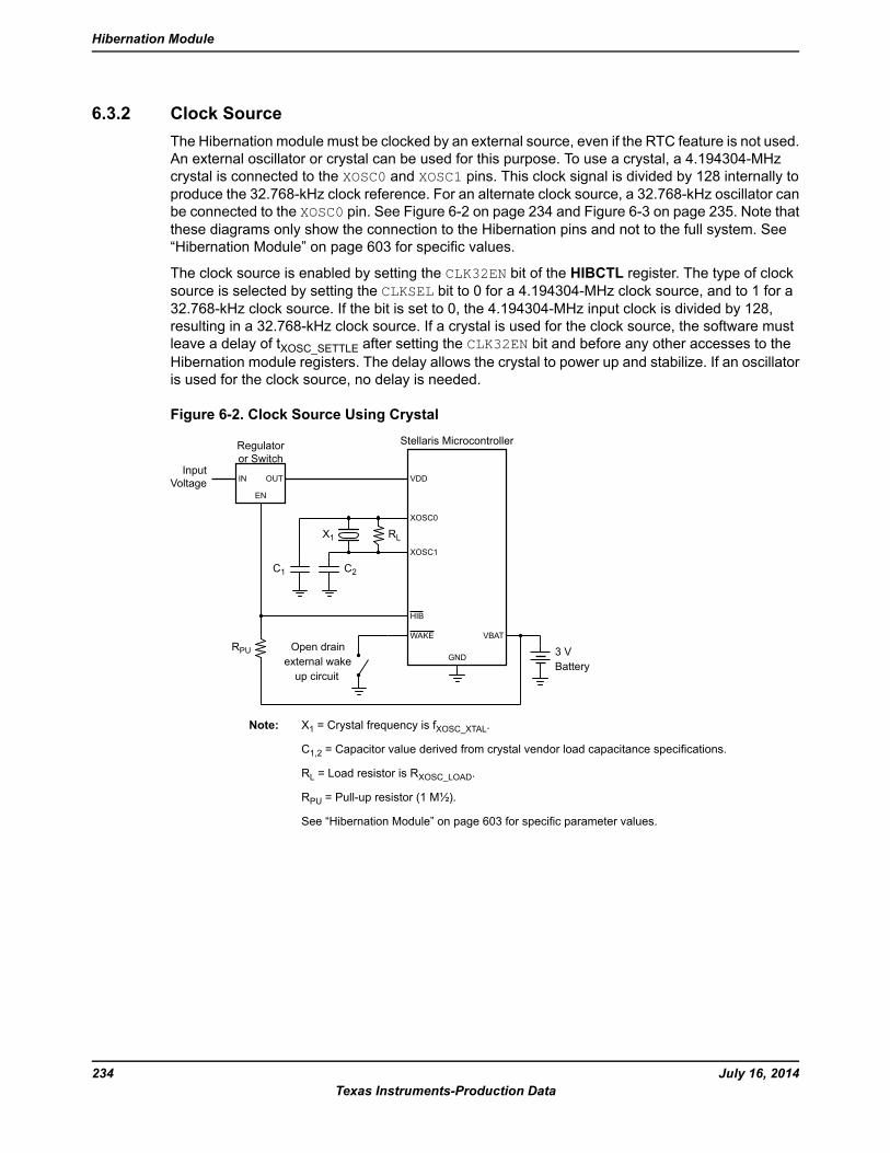
6.3.2 Clock SourceThe Hibernation module must be clocked by an external source, even if the RTC feature is not used.An external oscillator or crystal can be used for this purpose. To use a crystal, a 4.194304-MHzcrystal is connected to the XOSC0 and XOSC1 pins. This clock signal is divided by 128 internally toproduce the 32.768-kHz clock reference. For an alternate clock source, a 32.768-kHz oscillator canbe connected to the XOSC0 pin. See Figure 6-2 on page 234 and Figure 6-3 on page 235. Note thatthese diagrams only show the connection to the Hibernation pins and not to the full system. See“Hibernation Module” on page 603 for specific values.
The clock source is enabled by setting the CLK32EN bit of the HIBCTL register. The type of clocksource is selected by setting the CLKSEL bit to 0 for a 4.194304-MHz clock source, and to 1 for a32.768-kHz clock source. If the bit is set to 0, the 4.194304-MHz input clock is divided by 128,resulting in a 32.768-kHz clock source. If a crystal is used for the clock source, the software mustleave a delay of tXOSC_SETTLE after setting the CLK32EN bit and before any other accesses to theHibernation module registers. The delay allows the crystal to power up and stabilize. If an oscillatoris used for the clock source, no delay is needed.
Figure 6-2. Clock Source Using Crystal
Open drainexternal wakeup circuit
3 VBattery
GND
C2C1
RLX1
VBAT
EN
InputVoltage
Regulatoror Switch
XOSC1
XOSC0
VDD
HIB
WAKE
OUTIN
Stellaris Microcontroller
RPU
Note: X1 = Crystal frequency is fXOSC_XTAL.
C1,2 = Capacitor value derived from crystal vendor load capacitance specifications.
RL = Load resistor is RXOSC_LOAD.
RPU = Pull-up resistor (1 M½).
See “Hibernation Module” on page 603 for specific parameter values.
July 16, 2014234Texas Instruments-Production Data
Hibernation Module
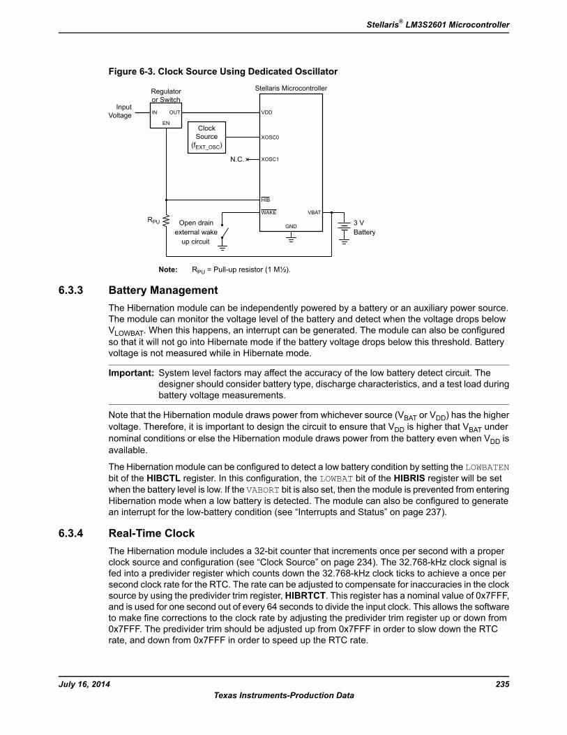
Figure 6-3. Clock Source Using Dedicated Oscillator
Open drainexternal wakeup circuit
EN
3 VBattery
GND
Stellaris Microcontroller
InputVoltage
Regulatoror Switch
ClockSource
(fEXT_OSC)
N.C. XOSC1
XOSC0
VDD
HIB
WAKE VBAT
OUTIN
RPU
Note: RPU = Pull-up resistor (1 M½).
6.3.3 Battery ManagementThe Hibernation module can be independently powered by a battery or an auxiliary power source.The module can monitor the voltage level of the battery and detect when the voltage drops belowVLOWBAT. When this happens, an interrupt can be generated. The module can also be configuredso that it will not go into Hibernate mode if the battery voltage drops below this threshold. Batteryvoltage is not measured while in Hibernate mode.
Important: System level factors may affect the accuracy of the low battery detect circuit. Thedesigner should consider battery type, discharge characteristics, and a test load duringbattery voltage measurements.
Note that the Hibernation module draws power from whichever source (VBAT or VDD) has the highervoltage. Therefore, it is important to design the circuit to ensure that VDD is higher that VBAT undernominal conditions or else the Hibernation module draws power from the battery even when VDD isavailable.
The Hibernation module can be configured to detect a low battery condition by setting the LOWBATENbit of the HIBCTL register. In this configuration, the LOWBAT bit of the HIBRIS register will be setwhen the battery level is low. If the VABORT bit is also set, then the module is prevented from enteringHibernation mode when a low battery is detected. The module can also be configured to generatean interrupt for the low-battery condition (see “Interrupts and Status” on page 237).
6.3.4 Real-Time ClockThe Hibernation module includes a 32-bit counter that increments once per second with a properclock source and configuration (see “Clock Source” on page 234). The 32.768-kHz clock signal isfed into a predivider register which counts down the 32.768-kHz clock ticks to achieve a once persecond clock rate for the RTC. The rate can be adjusted to compensate for inaccuracies in the clocksource by using the predivider trim register, HIBRTCT. This register has a nominal value of 0x7FFF,and is used for one second out of every 64 seconds to divide the input clock. This allows the softwareto make fine corrections to the clock rate by adjusting the predivider trim register up or down from0x7FFF. The predivider trim should be adjusted up from 0x7FFF in order to slow down the RTCrate, and down from 0x7FFF in order to speed up the RTC rate.
235July 16, 2014Texas Instruments-Production Data
Stellaris® LM3S2601 Microcontroller
The Hibernation module includes two 32-bit match registers that are compared to the value of theRTC counter. The match registers can be used to wake the processor from hibernation mode, orto generate an interrupt to the processor if it is not in hibernation.
The RTC must be enabled with the RTCEN bit of the HIBCTL register. The value of the RTC can beset at any time by writing to the HIBRTCLD register. The predivider trim can be adjusted by readingand writing theHIBRTCT register. The predivider uses this register once every 64 seconds to adjustthe clock rate. The two match registers can be set by writing to the HIBRTCM0 and HIBRTCM1registers. The RTC can be configured to generate interrupts by using the interrupt registers (see“Interrupts and Status” on page 237). As long as the RTC is enabled and a valid VBAT is present, theRTC continues counting, regardless of whether VDD is present or if the part is in hibernation.
6.3.5 Battery-Backed MemoryThe Hibernation module contains 64 32-bit words of memory which are retained during hibernation.This memory is powered from the battery or auxiliary power supply during hibernation. The processorsoftware can save state information in this memory prior to hibernation, and can then recover thestate upon waking. The battery-backed memory can be accessed through the HIBDATA registers.
6.3.6 Power Control
Important: The Hibernation Module requires special system implementation considerations whenusing HIB to control power, as it is intended to power-down all other sections of its hostdevice. All system signals and power supplies that connect to the chip must be drivento 0 VDC or powered down with the same regulator controlled by HIB. See “HibernationModule” on page 603 for more details.
The Hibernation module controls power to the microcontroller through the use of the HIB pin. Thispin is intended to be connected to the enable signal of the external regulator(s) providing 3.3 Vand/or 2.5 V to the microcontroller. When the HIB signal is asserted by the Hibernation module, theexternal regulator is turned off and no longer powers the system. The Hibernation module remainspowered from the VBAT supply (which could be a battery or an auxiliary power source) until a Wakeevent. Power to the device is restored by deasserting the HIB signal, which causes the externalregulator to turn power back on to the chip.
6.3.7 Initiating HibernateHibernation mode is initiated by the microcontroller setting the HIBREQ bit of the HIBCTL register.Prior to doing this, a wake-up condition must be configured, either from the external WAKE pin, orby using an RTC match.
The Hibernation module is configured to wake from the external WAKE pin by setting the PINWENbit of theHIBCTL register. It is configured to wake from RTCmatch by setting the RTCWEN bit. Eitherone or both of these bits can be set prior to going into hibernation. The WAKE pin includes a weakinternal pull-up. Note that both the HIB and WAKE pins use the Hibernation module's internal powersupply as the logic 1 reference.
When the Hibernation module wakes, the microcontroller will see a normal power-on reset. Softwarecan detect that the power-on was due to a wake from hibernation by examining the raw interruptstatus register (see “Interrupts and Status” on page 237) and by looking for state data in thebattery-backed memory (see “Battery-Backed Memory” on page 236).
When the HIB signal deasserts, enabling the external regulator, the external regulator must reachthe operating voltage within tHIB_TO_VDD.
July 16, 2014236Texas Instruments-Production Data
Hibernation Module
6.3.8 Interrupts and StatusThe Hibernation module can generate interrupts when the following conditions occur:
Assertion of WAKE pin
RTC match
Low battery detected
All of the interrupts are ORed together before being sent to the interrupt controller, so the Hibernatemodule can only generate a single interrupt request to the controller at any given time. The softwareinterrupt handler can service multiple interrupt events by reading the HIBMIS register. Software canalso read the status of the Hibernation module at any time by reading the HIBRIS register whichshows all of the pending events. This register can be used at power-on to see if a wake conditionis pending, which indicates to the software that a hibernation wake occurred.
The events that can trigger an interrupt are configured by setting the appropriate bits in the HIBIMregister. Pending interrupts can be cleared by writing the corresponding bit in the HIBIC register.
6.4 Initialization and ConfigurationThe Hibernation module can be set in several different configurations. The following sections showthe recommended programming sequence for various scenarios. The examples below assume thata 32.768-kHz oscillator is used, and thus always show bit 2 (CLKSEL) of the HIBCTL register setto 1. If a 4.194304-MHz crystal is used instead, then the CLKSEL bit remains cleared. Because theHibernation module runs at 32.768 kHz and is asynchronous to the rest of the system, softwaremust allow a delay of tHIB_REG_WRITE after writes to certain registers (see “Register AccessTiming” on page 233). The registers that require a delay are listed in a note in “RegisterMap” on page 238 as well as in each register description.
6.4.1 InitializationThe Hibernation module clock source must be enabled first, even if the RTC feature is not used. Ifa 4.194304-MHz crystal is used, perform the following steps:
1. Write 0x40 to theHIBCTL register at offset 0x10 to enable the crystal and select the divide-by-128input path.
2. Wait for a time of tXOSC_SETTLE for the crystal to power up and stabilize before performing anyother operations with the Hibernation module.
If a 32.678-kHz oscillator is used, then perform the following steps:
1. Write 0x44 to the HIBCTL register at offset 0x10 to enable the oscillator input.
2. No delay is necessary.
The above is only necessary when the entire system is initialized for the first time. If the processoris powered due to a wake from hibernation, then the Hibernation module has already been poweredup and the above steps are not necessary. The software can detect that the Hibernation moduleand clock are already powered by examining the CLK32EN bit of the HIBCTL register.
6.4.2 RTC Match Functionality (No Hibernation)Use the following steps to implement the RTC match functionality of the Hibernation module:
237July 16, 2014Texas Instruments-Production Data
Stellaris® LM3S2601 Microcontroller
1. Write the required RTCmatch value to one of theHIBRTCMn registers at offset 0x004 or 0x008.
2. Write the required RTC load value to the HIBRTCLD register at offset 0x00C.
3. Set the required RTC match interrupt mask in the RTCALT0 and RTCALT1 bits (bits 1:0) in theHIBIM register at offset 0x014.
4. Write 0x0000.0041 to the HIBCTL register at offset 0x010 to enable the RTC to begin counting.
6.4.3 RTC Match/Wake-Up from HibernationUse the following steps to implement the RTC match and wake-up functionality of the Hibernationmodule:
1. Write the required RTC match value to the HIBRTCMn registers at offset 0x004 or 0x008.
2. Write the required RTC load value to the HIBRTCLD register at offset 0x00C.
3. Write any data to be retained during power cut to theHIBDATA register at offsets 0x030-0x12C.
4. Set the RTC Match Wake-Up and start the hibernation sequence by writing 0x0000.004F to theHIBCTL register at offset 0x010.
6.4.4 External Wake-Up from HibernationUse the following steps to implement the Hibernation module with the external WAKE pin as thewake-up source for the microcontroller:
1. Write any data to be retained during power cut to theHIBDATA register at offsets 0x030-0x12C.
2. Enable the external wake and start the hibernation sequence by writing 0x0000.0056 to theHIBCTL register at offset 0x010.
6.4.5 RTC/External Wake-Up from Hibernation
1. Write the required RTC match value to the HIBRTCMn registers at offset 0x004 or 0x008.
2. Write the required RTC load value to the HIBRTCLD register at offset 0x00C.
3. Write any data to be retained during power cut to theHIBDATA register at offsets 0x030-0x12C.
4. Set the RTCMatch/ExternalWake-Up and start the hibernation sequence by writing 0x0000.005Fto the HIBCTL register at offset 0x010.
6.5 Register MapTable 6-3 on page 239 lists the Hibernation registers. All addresses given are relative to the HibernationModule base address at 0x400F.C000. Note that the Hibernation module clock must be enabledbefore the registers can be programmed (see page 206). There must be a delay of 3 system clocksafter the Hibernation module clock is enabled before any Hibernation module registers are accessed.
Important: The Hibernation module registers are reset under two conditions:
1. A system reset when the RTCEN and the PINWEN bits in the HIBCTL register areboth cleared.
July 16, 2014238Texas Instruments-Production Data
Hibernation Module
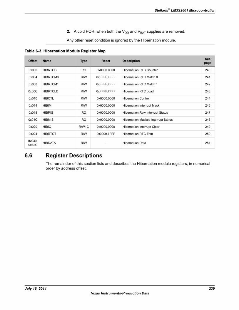
2. A cold POR, when both the VDD and VBAT supplies are removed.
Any other reset condition is ignored by the Hibernation module.
Table 6-3. Hibernation Module Register Map
SeepageDescriptionResetTypeNameOffset
240Hibernation RTC Counter0x0000.0000ROHIBRTCC0x000
241Hibernation RTC Match 00xFFFF.FFFFR/WHIBRTCM00x004
242Hibernation RTC Match 10xFFFF.FFFFR/WHIBRTCM10x008
243Hibernation RTC Load0xFFFF.FFFFR/WHIBRTCLD0x00C
244Hibernation Control0x8000.0000R/WHIBCTL0x010
246Hibernation Interrupt Mask0x0000.0000R/WHIBIM0x014
247Hibernation Raw Interrupt Status0x0000.0000ROHIBRIS0x018
248Hibernation Masked Interrupt Status0x0000.0000ROHIBMIS0x01C
249Hibernation Interrupt Clear0x0000.0000R/W1CHIBIC0x020
250Hibernation RTC Trim0x0000.7FFFR/WHIBRTCT0x024
251Hibernation Data-R/WHIBDATA0x030-0x12C
6.6 Register DescriptionsThe remainder of this section lists and describes the Hibernation module registers, in numericalorder by address offset.
239July 16, 2014Texas Instruments-Production Data
Stellaris® LM3S2601 Microcontroller
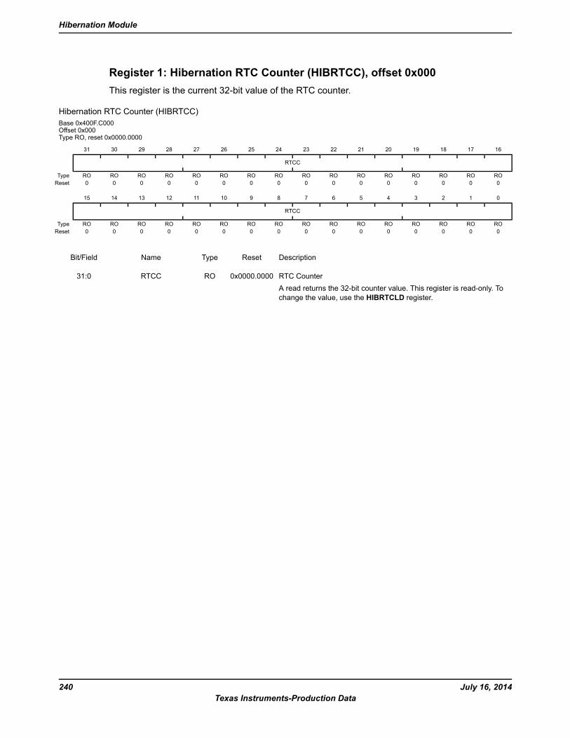
Register 1: Hibernation RTC Counter (HIBRTCC), offset 0x000This register is the current 32-bit value of the RTC counter.
Hibernation RTC Counter (HIBRTCC)Base 0x400F.C000Offset 0x000Type RO, reset 0x0000.0000
16171819202122232425262728293031
RTCC
ROROROROROROROROROROROROROROROROType0000000000000000Reset
0123456789101112131415
RTCC
ROROROROROROROROROROROROROROROROType0000000000000000Reset
DescriptionResetTypeNameBit/Field
RTC CounterA read returns the 32-bit counter value. This register is read-only. Tochange the value, use the HIBRTCLD register.
0x0000.0000RORTCC31:0
July 16, 2014240Texas Instruments-Production Data
Hibernation Module
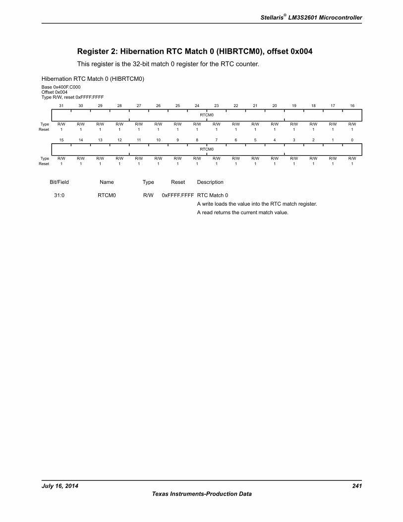
Register 2: Hibernation RTC Match 0 (HIBRTCM0), offset 0x004This register is the 32-bit match 0 register for the RTC counter.
Hibernation RTC Match 0 (HIBRTCM0)Base 0x400F.C000Offset 0x004Type R/W, reset 0xFFFF.FFFF
16171819202122232425262728293031
RTCM0
R/WR/WR/WR/WR/WR/WR/WR/WR/WR/WR/WR/WR/WR/WR/WR/WType1111111111111111Reset
0123456789101112131415
RTCM0
R/WR/WR/WR/WR/WR/WR/WR/WR/WR/WR/WR/WR/WR/WR/WR/WType1111111111111111Reset
DescriptionResetTypeNameBit/Field
RTC Match 0A write loads the value into the RTC match register.A read returns the current match value.
0xFFFF.FFFFR/WRTCM031:0
241July 16, 2014Texas Instruments-Production Data
Stellaris® LM3S2601 Microcontroller
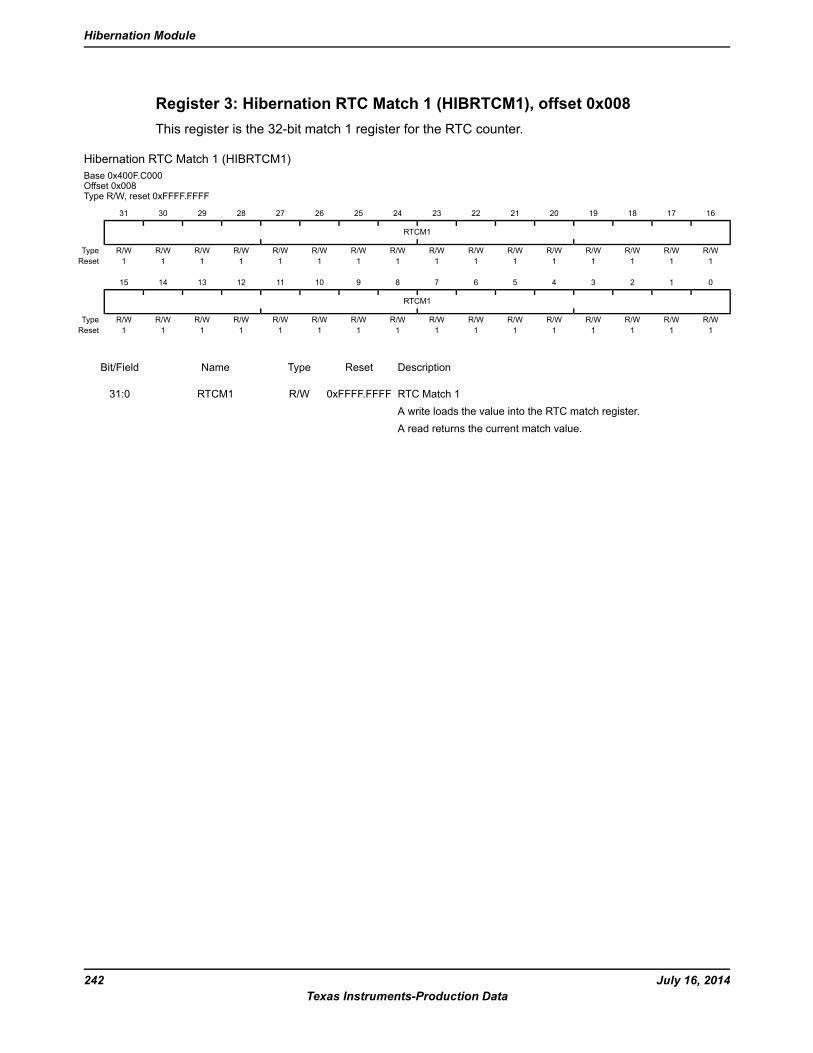
Register 3: Hibernation RTC Match 1 (HIBRTCM1), offset 0x008This register is the 32-bit match 1 register for the RTC counter.
Hibernation RTC Match 1 (HIBRTCM1)Base 0x400F.C000Offset 0x008Type R/W, reset 0xFFFF.FFFF
16171819202122232425262728293031
RTCM1
R/WR/WR/WR/WR/WR/WR/WR/WR/WR/WR/WR/WR/WR/WR/WR/WType1111111111111111Reset
0123456789101112131415
RTCM1
R/WR/WR/WR/WR/WR/WR/WR/WR/WR/WR/WR/WR/WR/WR/WR/WType1111111111111111Reset
DescriptionResetTypeNameBit/Field
RTC Match 1A write loads the value into the RTC match register.A read returns the current match value.
0xFFFF.FFFFR/WRTCM131:0
July 16, 2014242Texas Instruments-Production Data
Hibernation Module
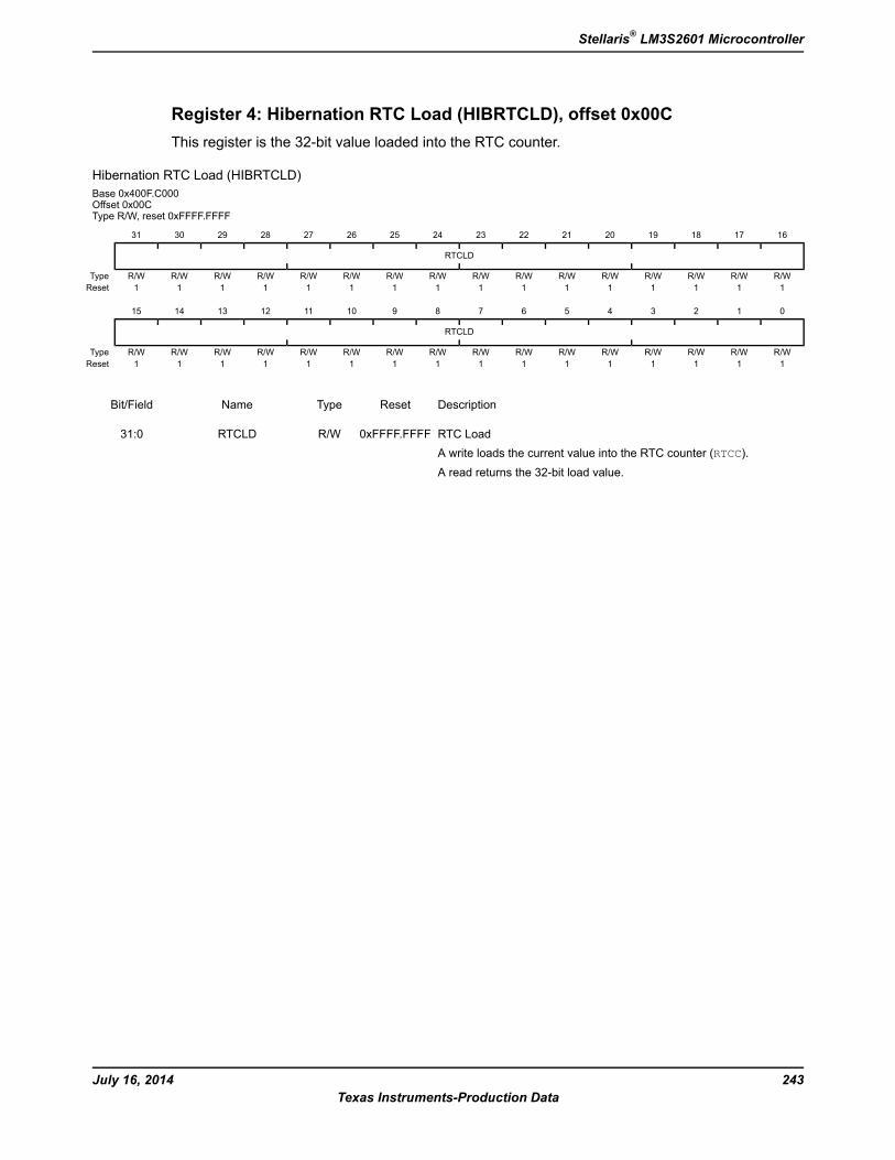
Register 4: Hibernation RTC Load (HIBRTCLD), offset 0x00CThis register is the 32-bit value loaded into the RTC counter.
Hibernation RTC Load (HIBRTCLD)Base 0x400F.C000Offset 0x00CType R/W, reset 0xFFFF.FFFF
16171819202122232425262728293031
RTCLD
R/WR/WR/WR/WR/WR/WR/WR/WR/WR/WR/WR/WR/WR/WR/WR/WType1111111111111111Reset
0123456789101112131415
RTCLD
R/WR/WR/WR/WR/WR/WR/WR/WR/WR/WR/WR/WR/WR/WR/WR/WType1111111111111111Reset
DescriptionResetTypeNameBit/Field
RTC LoadA write loads the current value into the RTC counter (RTCC).A read returns the 32-bit load value.
0xFFFF.FFFFR/WRTCLD31:0
243July 16, 2014Texas Instruments-Production Data
Stellaris® LM3S2601 Microcontroller
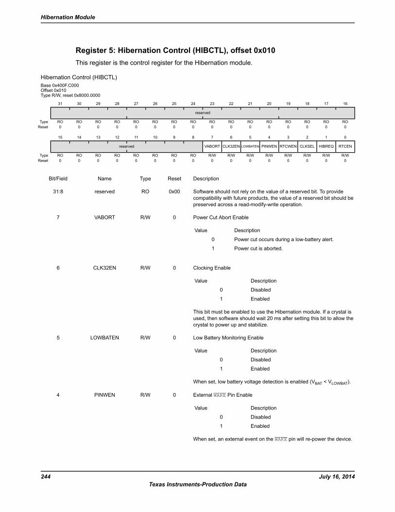
Register 5: Hibernation Control (HIBCTL), offset 0x010This register is the control register for the Hibernation module.
Hibernation Control (HIBCTL)Base 0x400F.C000Offset 0x010Type R/W, reset 0x8000.0000
16171819202122232425262728293031
reserved
ROROROROROROROROROROROROROROROROType0000000000000000Reset
0123456789101112131415
RTCENHIBREQCLKSELRTCWENPINWENLOWBATENCLK32ENVABORTreserved
R/WR/WR/WR/WR/WR/WR/WR/WROROROROROROROROType0000000000000000Reset
DescriptionResetTypeNameBit/Field
Software should not rely on the value of a reserved bit. To providecompatibility with future products, the value of a reserved bit should bepreserved across a read-modify-write operation.
0x00ROreserved31:8
Power Cut Abort Enable
DescriptionValue
Power cut occurs during a low-battery alert.0
Power cut is aborted.1
0R/WVABORT7
Clocking Enable
DescriptionValue
Disabled0
Enabled1
This bit must be enabled to use the Hibernation module. If a crystal isused, then software should wait 20 ms after setting this bit to allow thecrystal to power up and stabilize.
0R/WCLK32EN6
Low Battery Monitoring Enable
DescriptionValue
Disabled0
Enabled1
When set, low battery voltage detection is enabled (VBAT < VLOWBAT).
0R/WLOWBATEN5
External WAKE Pin Enable
DescriptionValue
Disabled0
Enabled1
When set, an external event on the WAKE pin will re-power the device.
0R/WPINWEN4
July 16, 2014244Texas Instruments-Production Data
Hibernation Module
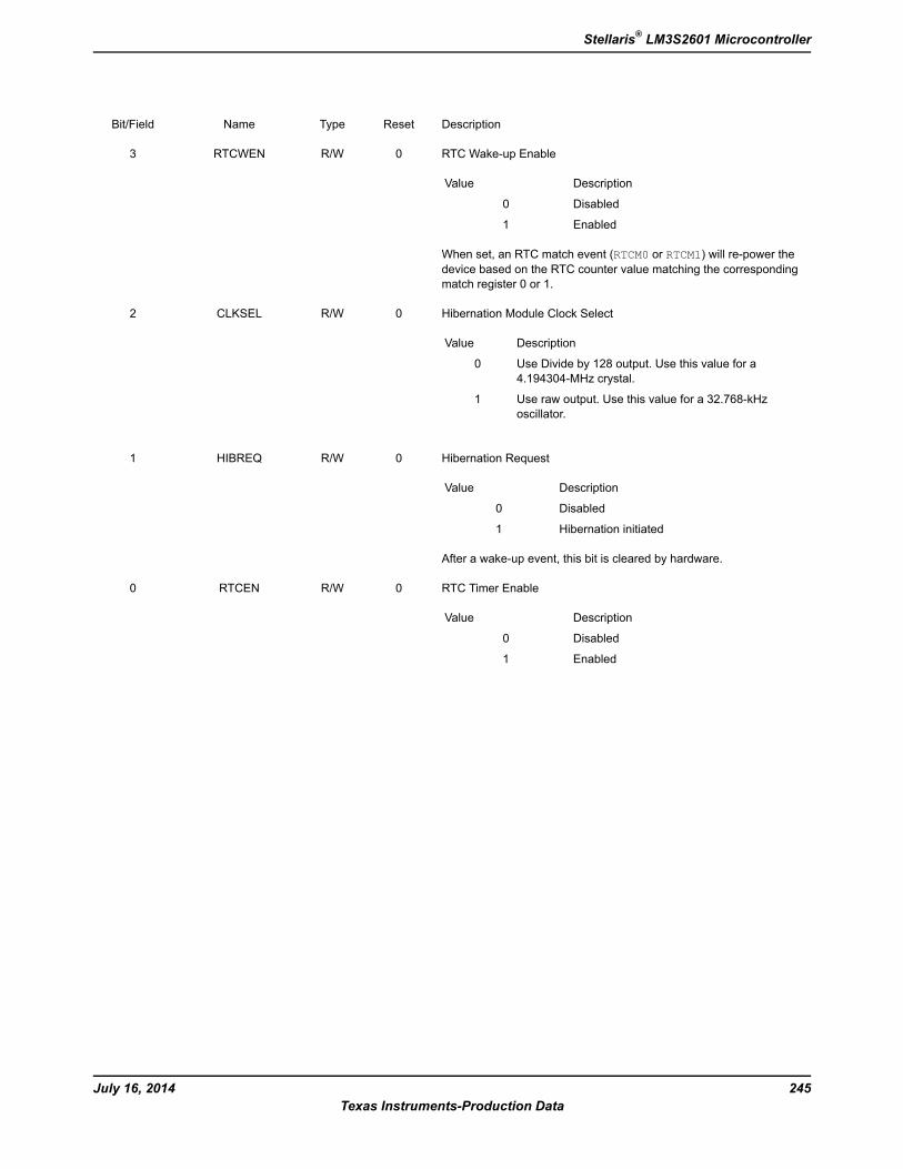
DescriptionResetTypeNameBit/Field
RTC Wake-up Enable
DescriptionValue
Disabled0
Enabled1
When set, an RTC match event (RTCM0 or RTCM1) will re-power thedevice based on the RTC counter value matching the correspondingmatch register 0 or 1.
0R/WRTCWEN3
Hibernation Module Clock Select
DescriptionValue
Use Divide by 128 output. Use this value for a4.194304-MHz crystal.
0
Use raw output. Use this value for a 32.768-kHzoscillator.
1
0R/WCLKSEL2
Hibernation Request
DescriptionValue
Disabled0
Hibernation initiated1
After a wake-up event, this bit is cleared by hardware.
0R/WHIBREQ1
RTC Timer Enable
DescriptionValue
Disabled0
Enabled1
0R/WRTCEN0
245July 16, 2014Texas Instruments-Production Data
Stellaris® LM3S2601 Microcontroller
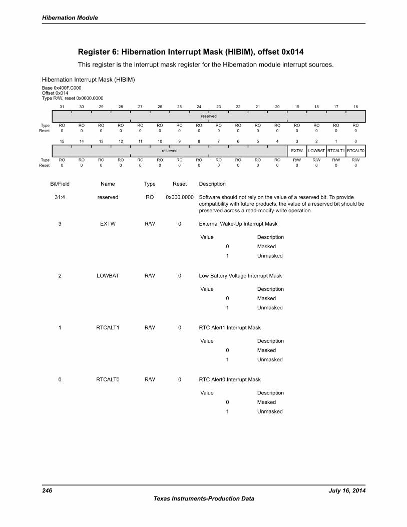
Register 6: Hibernation Interrupt Mask (HIBIM), offset 0x014This register is the interrupt mask register for the Hibernation module interrupt sources.
Hibernation Interrupt Mask (HIBIM)Base 0x400F.C000Offset 0x014Type R/W, reset 0x0000.0000
16171819202122232425262728293031
reserved
ROROROROROROROROROROROROROROROROType0000000000000000Reset
0123456789101112131415
RTCALT0RTCALT1LOWBATEXTWreserved
R/WR/WR/WR/WROROROROROROROROROROROROType0000000000000000Reset
DescriptionResetTypeNameBit/Field
Software should not rely on the value of a reserved bit. To providecompatibility with future products, the value of a reserved bit should bepreserved across a read-modify-write operation.
0x000.0000ROreserved31:4
External Wake-Up Interrupt Mask
DescriptionValue
Masked0
Unmasked1
0R/WEXTW3
Low Battery Voltage Interrupt Mask
DescriptionValue
Masked0
Unmasked1
0R/WLOWBAT2
RTC Alert1 Interrupt Mask
DescriptionValue
Masked0
Unmasked1
0R/WRTCALT11
RTC Alert0 Interrupt Mask
DescriptionValue
Masked0
Unmasked1
0R/WRTCALT00
July 16, 2014246Texas Instruments-Production Data
Hibernation Module
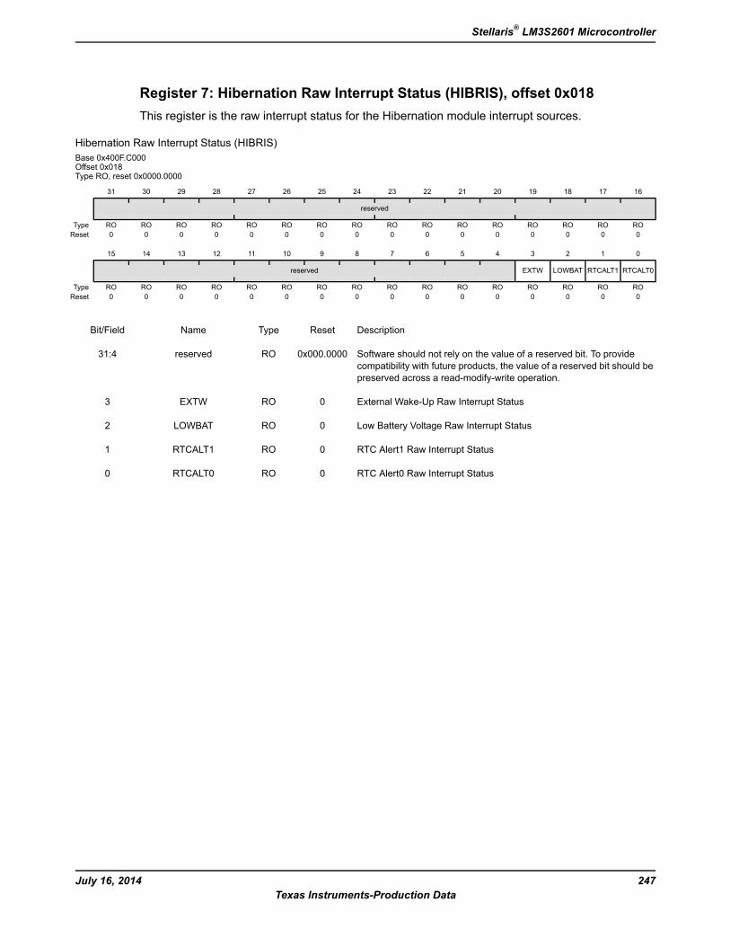
Register 7: Hibernation Raw Interrupt Status (HIBRIS), offset 0x018This register is the raw interrupt status for the Hibernation module interrupt sources.
Hibernation Raw Interrupt Status (HIBRIS)Base 0x400F.C000Offset 0x018Type RO, reset 0x0000.0000
16171819202122232425262728293031
reserved
ROROROROROROROROROROROROROROROROType0000000000000000Reset
0123456789101112131415
RTCALT0RTCALT1LOWBATEXTWreserved
ROROROROROROROROROROROROROROROROType0000000000000000Reset
DescriptionResetTypeNameBit/Field
Software should not rely on the value of a reserved bit. To providecompatibility with future products, the value of a reserved bit should bepreserved across a read-modify-write operation.
0x000.0000ROreserved31:4
External Wake-Up Raw Interrupt Status0ROEXTW3
Low Battery Voltage Raw Interrupt Status0ROLOWBAT2
RTC Alert1 Raw Interrupt Status0RORTCALT11
RTC Alert0 Raw Interrupt Status0RORTCALT00
247July 16, 2014Texas Instruments-Production Data
Stellaris® LM3S2601 Microcontroller
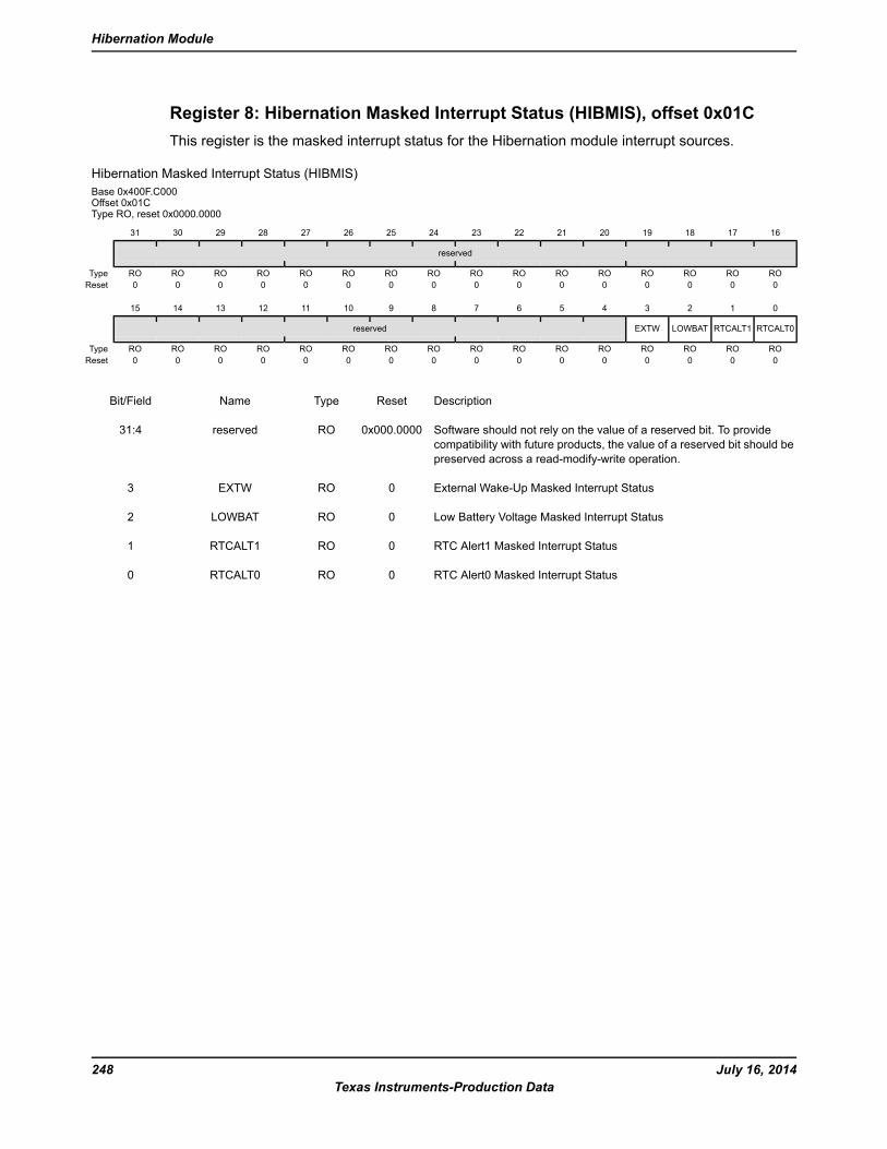
Register 8: Hibernation Masked Interrupt Status (HIBMIS), offset 0x01CThis register is the masked interrupt status for the Hibernation module interrupt sources.
Hibernation Masked Interrupt Status (HIBMIS)Base 0x400F.C000Offset 0x01CType RO, reset 0x0000.0000
16171819202122232425262728293031
reserved
ROROROROROROROROROROROROROROROROType0000000000000000Reset
0123456789101112131415
RTCALT0RTCALT1LOWBATEXTWreserved
ROROROROROROROROROROROROROROROROType0000000000000000Reset
DescriptionResetTypeNameBit/Field
Software should not rely on the value of a reserved bit. To providecompatibility with future products, the value of a reserved bit should bepreserved across a read-modify-write operation.
0x000.0000ROreserved31:4
External Wake-Up Masked Interrupt Status0ROEXTW3
Low Battery Voltage Masked Interrupt Status0ROLOWBAT2
RTC Alert1 Masked Interrupt Status0RORTCALT11
RTC Alert0 Masked Interrupt Status0RORTCALT00
July 16, 2014248Texas Instruments-Production Data
Hibernation Module
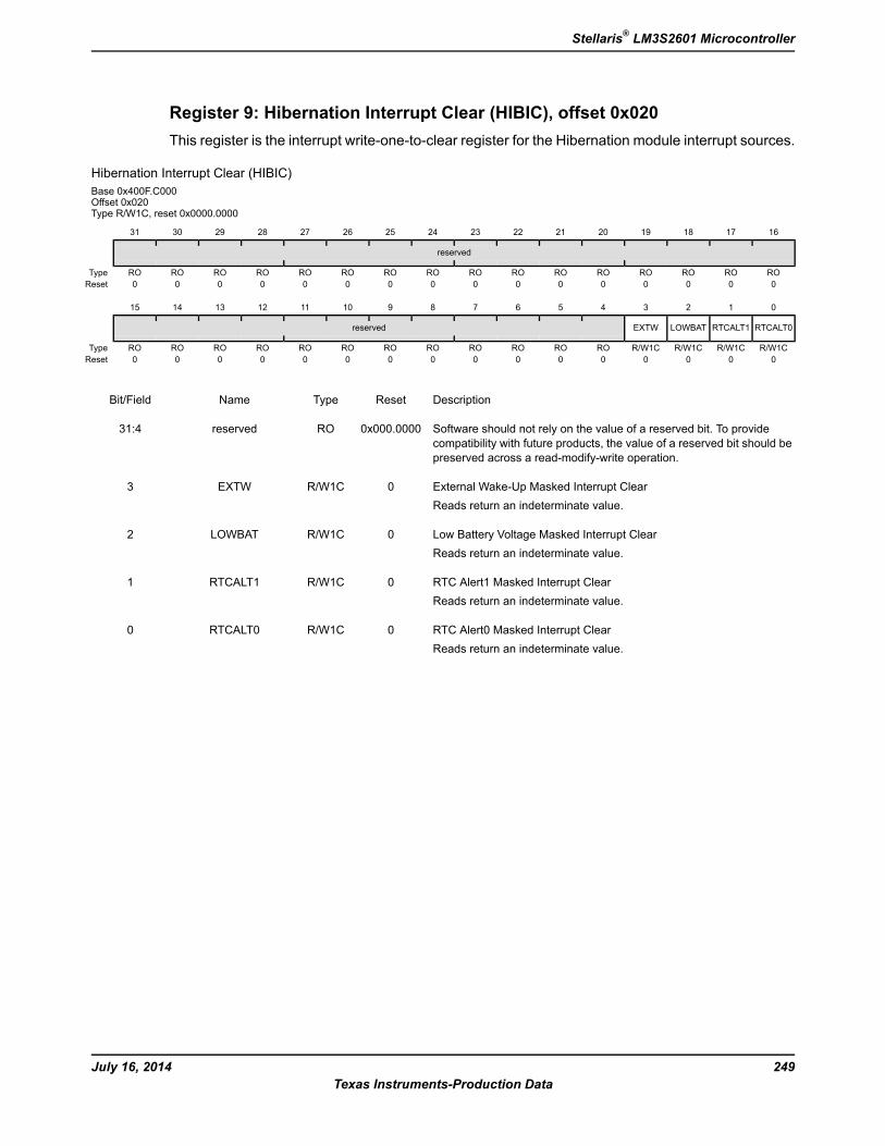
Register 9: Hibernation Interrupt Clear (HIBIC), offset 0x020This register is the interrupt write-one-to-clear register for the Hibernation module interrupt sources.
Hibernation Interrupt Clear (HIBIC)Base 0x400F.C000Offset 0x020Type R/W1C, reset 0x0000.0000
16171819202122232425262728293031
reserved
ROROROROROROROROROROROROROROROROType0000000000000000Reset
0123456789101112131415
RTCALT0RTCALT1LOWBATEXTWreserved
R/W1CR/W1CR/W1CR/W1CROROROROROROROROROROROROType0000000000000000Reset
DescriptionResetTypeNameBit/Field
Software should not rely on the value of a reserved bit. To providecompatibility with future products, the value of a reserved bit should bepreserved across a read-modify-write operation.
0x000.0000ROreserved31:4
External Wake-Up Masked Interrupt ClearReads return an indeterminate value.
0R/W1CEXTW3
Low Battery Voltage Masked Interrupt ClearReads return an indeterminate value.
0R/W1CLOWBAT2
RTC Alert1 Masked Interrupt ClearReads return an indeterminate value.
0R/W1CRTCALT11
RTC Alert0 Masked Interrupt ClearReads return an indeterminate value.
0R/W1CRTCALT00
249July 16, 2014Texas Instruments-Production Data
Stellaris® LM3S2601 Microcontroller
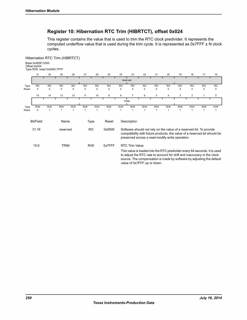
Register 10: Hibernation RTC Trim (HIBRTCT), offset 0x024This register contains the value that is used to trim the RTC clock predivider. It represents thecomputed underflow value that is used during the trim cycle. It is represented as 0x7FFF ± N clockcycles.
Hibernation RTC Trim (HIBRTCT)Base 0x400F.C000Offset 0x024Type R/W, reset 0x0000.7FFF
16171819202122232425262728293031
reserved
ROROROROROROROROROROROROROROROROType0000000000000000Reset
0123456789101112131415
TRIM
R/WR/WR/WR/WR/WR/WR/WR/WR/WR/WR/WR/WR/WR/WR/WR/WType1111111111111110Reset
DescriptionResetTypeNameBit/Field
Software should not rely on the value of a reserved bit. To providecompatibility with future products, the value of a reserved bit should bepreserved across a read-modify-write operation.
0x0000ROreserved31:16
RTC Trim ValueThis value is loaded into the RTC predivider every 64 seconds. It is usedto adjust the RTC rate to account for drift and inaccuracy in the clocksource. The compensation is made by software by adjusting the defaultvalue of 0x7FFF up or down.
0x7FFFR/WTRIM15:0
July 16, 2014250Texas Instruments-Production Data
Hibernation Module
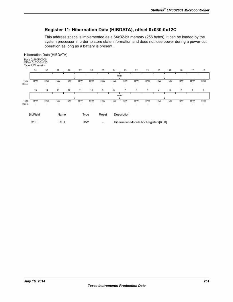
Register 11: Hibernation Data (HIBDATA), offset 0x030-0x12CThis address space is implemented as a 64x32-bit memory (256 bytes). It can be loaded by thesystem processor in order to store state information and does not lose power during a power-cutoperation as long as a battery is present.
Hibernation Data (HIBDATA)Base 0x400F.C000Offset 0x030-0x12CType R/W, reset -
16171819202122232425262728293031
RTD
R/WR/WR/WR/WR/WR/WR/WR/WR/WR/WR/WR/WR/WR/WR/WR/WType----------------Reset
0123456789101112131415
RTD
R/WR/WR/WR/WR/WR/WR/WR/WR/WR/WR/WR/WR/WR/WR/WR/WType----------------Reset
DescriptionResetTypeNameBit/Field
Hibernation Module NV Registers[63:0]-R/WRTD31:0
251July 16, 2014Texas Instruments-Production Data
Stellaris® LM3S2601 Microcontroller
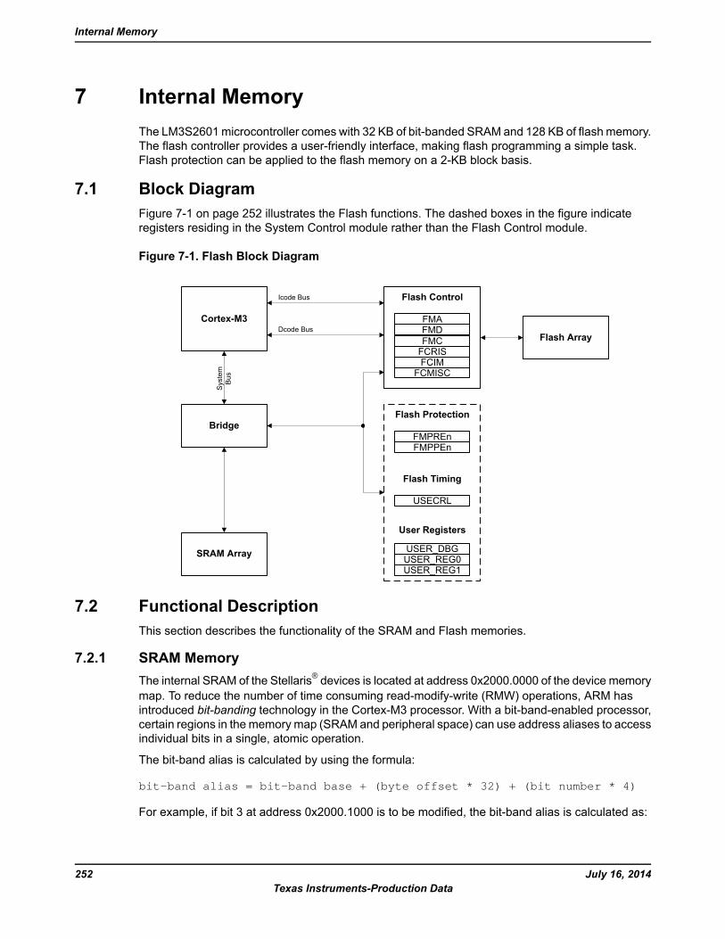
7 Internal MemoryThe LM3S2601microcontroller comes with 32 KB of bit-banded SRAM and 128 KB of flash memory.The flash controller provides a user-friendly interface, making flash programming a simple task.Flash protection can be applied to the flash memory on a 2-KB block basis.
7.1 Block DiagramFigure 7-1 on page 252 illustrates the Flash functions. The dashed boxes in the figure indicateregisters residing in the System Control module rather than the Flash Control module.
Figure 7-1. Flash Block Diagram
Flash Control
FMAFMD
FCIMFCMISC
Flash Array
Cortex-M3
Bridge
SRAM Array
System
Bus
Icode Bus
Dcode Bus
Flash Protection
FMPREnFMPPEn
Flash Timing
USECRL
User Registers
USER_DBGUSER_REG0USER_REG1
FMCFCRIS
7.2 Functional DescriptionThis section describes the functionality of the SRAM and Flash memories.
7.2.1 SRAM MemoryThe internal SRAM of the Stellaris® devices is located at address 0x2000.0000 of the device memorymap. To reduce the number of time consuming read-modify-write (RMW) operations, ARM hasintroduced bit-banding technology in the Cortex-M3 processor. With a bit-band-enabled processor,certain regions in thememory map (SRAM and peripheral space) can use address aliases to accessindividual bits in a single, atomic operation.
The bit-band alias is calculated by using the formula:
bit-band alias = bit-band base + (byte offset * 32) + (bit number * 4)
For example, if bit 3 at address 0x2000.1000 is to be modified, the bit-band alias is calculated as:
July 16, 2014252Texas Instruments-Production Data
Internal Memory
0x2200.0000 + (0x1000 * 32) + (3 * 4) = 0x2202.000C
With the alias address calculated, an instruction performing a read/write to address 0x2202.000Callows direct access to only bit 3 of the byte at address 0x2000.1000.
For details about bit-banding, see “Bit-Banding” on page 69.
7.2.2 Flash MemoryThe flash is organized as a set of 1-KB blocks that can be individually erased. Erasing a blockcauses the entire contents of the block to be reset to all 1s. An individual 32-bit word can beprogrammed to change bits that are currently 1 to a 0. These blocks are paired into a set of 2-KBblocks that can be individually protected. The protection allows blocks to be marked as read-onlyor execute-only, providing different levels of code protection. Read-only blocks cannot be erasedor programmed, protecting the contents of those blocks from being modified. Execute-only blockscannot be erased or programmed, and can only be read by the controller instruction fetch mechanism,protecting the contents of those blocks from being read by either the controller or by a debugger.
See also “Serial Flash Loader” on page 608 for a preprogrammed flash-resident utility used todownload code to the flash memory of a device without the use of a debug interface.
7.2.2.1 Flash Memory TimingThe timing for the flash is automatically handled by the flash controller. However, in order to do so,it must know the clock rate of the system in order to time its internal signals properly. The numberof clock cycles per microsecond must be provided to the flash controller for it to accomplish thistiming. It is software's responsibility to keep the flash controller updated with this information via theUSec Reload (USECRL) register.
On reset, theUSECRL register is loaded with a value that configures the flash timing so that it workswith the maximum clock rate of the part. If software changes the system operating frequency, thenew operating frequency minus 1 (in MHz) must be loaded into USECRL before any flashmodifications are attempted. For example, if the device is operating at a speed of 20 MHz, a valueof 0x13 (20-1) must be written to the USECRL register.
7.2.2.2 Flash Memory ProtectionThe user is provided two forms of flash protection per 2-KB flash blocks in two pairs of 32-bit wideregisters. The protection policy for each form is controlled by individual bits (per policy per block)in the FMPPEn and FMPREn registers.
Flash Memory Protection Program Enable (FMPPEn): If set, the block may be programmed(written) or erased. If cleared, the block may not be changed.
Flash Memory Protection Read Enable (FMPREn): If a bit is set, the corresponding block maybe executed or read by software or debuggers. If a bit is cleared, the corresponding block mayonly be executed, and contents of the memory block are prohibited from being read as data.
The policies may be combined as shown in Table 7-1 on page 253.
Table 7-1. Flash Protection Policy Combinations
ProtectionFMPREnFMPPEn
Execute-only protection. The block may only be executed and may not be written or erased.This mode is used to protect code.
00
253July 16, 2014Texas Instruments-Production Data
Stellaris® LM3S2601 Microcontroller
Table 7-1. Flash Protection Policy Combinations (continued)
ProtectionFMPREnFMPPEn
The block may be written, erased or executed, but not read. This combination is unlikely tobe used.
01
Read-only protection. The block may be read or executed but may not be written or erased.This mode is used to lock the block from further modification while allowing any read orexecute access.
10
No protection. The block may be written, erased, executed or read.11
A Flashmemory access that attempts to read a read-protected block (FMPREn bit is set) is prohibitedand generates a bus fault. A Flash memory access that attempts to program or erase aprogram-protected block (FMPPEn bit is set) is prohibited and can optionally generate an interrupt(by setting the AMASK bit in the Flash Controller Interrupt Mask (FCIM) register) to alert softwaredevelopers of poorly behaving software during the development and debug phases.
The factory settings for the FMPREn and FMPPEn registers are a value of 1 for all implementedbanks. These settings create a policy of open access and programmability. The register bits maybe changed by clearing the specific register bit. The changes are not permanent until the registeris committed (saved), at which point the bit change is permanent. If a bit is changed from a 1 to a0 and not committed, it may be restored by executing a power-on reset sequence. The changesare committed using the Flash Memory Control (FMC) register. Details on programming these bitsare discussed in “Nonvolatile Register Programming” on page 256.
7.2.2.3 Execute-Only ProtectionExecute-only protection prevents both modification and visibility to a protected flash block. Thismode is intended to be used in situations where a device requires debug capability, yet portions ofthe application space must be protected from external access. An example of this is a companywho wishes to sell Stellaris devices with their proprietary software pre-programmed, yet allow theend user to add custom code to an unprotected region of the flash (such as a motor control modulewith a customizable motor configuration section in flash).
Literal data introduces a complication to the protection mechanism. When C code is compiled andlinked, literal data (constants, and so on) is typically placed in the text section, between functions,by the compiler. The literal data is accessed at run time through the use of the LDR instruction,which loads the data from memory using a PC-relative memory address. The execution of the LDRinstruction generates a read transaction across the Cortex-M3's DCode bus, which is subject to theexecute-only protection mechanism. If the accessed block is marked as execute only, the transactionis blocked, and the processor is prevented from loading the constant data and, therefore, inhibitingcorrect execution. Therefore, using execute-only protection requires that literal data be handleddifferently. There are three ways to address this:
1. Use a compiler that allows literal data to be collected into a separate section that is put into oneor more read-enabled flash blocks. Note that the LDR instruction may use a PC-relativeaddress–-in which case the literal pool cannot be located outside the span of the offset–-or thesoftware may reserve a register to point to the base address of the literal pool and the LDRoffset is relative to the beginning of the pool.
2. Use a compiler that generates literal data from arithmetic instruction immediate data andsubsequent computation.
3. Use method 1 or 2, but in assembly language, if the compiler does not support either method.
July 16, 2014254Texas Instruments-Production Data
Internal Memory
7.2.2.4 Read-Only ProtectionRead-only protection prevents the contents of the flash block from being re-programmed, while stillallowing the content to be read by processor or the debug interface. Note that if a FMPREn bit iscleared, all read accesses to the Flash memory block are disallowed, including any data accesses.Care must be taken not to store required data in a Flash memory block that has the associatedFMPREn bit cleared.
The read-only mode does not prevent read access to the stored program, but it does provideprotection against accidental (or malicious) erasure or programming. Read-only is especially usefulfor utilities like the boot loader when the debug interface is permanently disabled. In suchcombinations, the boot loader, which provides access control to the Flash memory, is protectedfrom being erased or modified.
7.2.2.5 Permanently Disabling DebugFor extremely sensitive applications, the debug interface to the processor and peripherals can bepermanently disabled, blocking all accesses to the device through the JTAG or SWD interfaces.With the debug interface disabled, it is still possible to perform standard IEEE instructions (such asboundary scan operations), but access to the processor and peripherals is blocked.
The DBG0 and DBG1 bits of the User Debug (USER_DBG) register control whether the debuginterface is turned on or off.
The debug interface should not be permanently disabled without providing some mechanism–-suchas the boot loader–-to provide customer-installable updates or bug fixes. Disabling the debuginterface is permanent and cannot be reversed.
7.2.2.6 InterruptsThe Flash memory controller can generate interrupts when the following conditions are observed:
Programming Interrupt - signals when a program or erase action is complete.
Access Interrupt - signals when a program or erase action has been attempted on a 2-kB blockof memory that is protected by its corresponding FMPPEn bit.
The interrupt events that can trigger a controller-level interrupt are defined in the Flash ControllerMasked Interrupt Status (FCMIS) register (see page 264) by setting the corresponding MASK bits.If interrupts are not used, the raw interrupt status is always visible via the Flash Controller RawInterrupt Status (FCRIS) register (see page 263).
Interrupts are always cleared (for both the FCMIS and FCRIS registers) by writing a 1 to thecorresponding bit in the Flash Controller Masked Interrupt Status and Clear (FCMISC) register(see page 265).
7.3 Flash Memory Initialization and Configuration
7.3.1 Flash ProgrammingThe Stellaris devices provide a user-friendly interface for flash programming. All erase/programoperations are handled via three registers: FMA, FMD, and FMC.
During a Flash memory operation (write, page erase, or mass erase) access to the Flash memoryis inhibited. As a result, instruction and literal fetches are held off until the Flash memory operationis complete. If instruction execution is required during a Flash memory operation, the code that isexecuting must be placed in SRAM and executed from there while the flash operation is in progress.
255July 16, 2014Texas Instruments-Production Data
Stellaris® LM3S2601 Microcontroller
7.3.1.1 To program a 32-bit word
1. Write source data to the FMD register.
2. Write the target address to the FMA register.
3. Write the flash write key and the WRITE bit (a value of 0xA442.0001) to the FMC register.
4. Poll the FMC register until the WRITE bit is cleared.
7.3.1.2 To perform an erase of a 1-KB page
1. Write the page address to the FMA register.
2. Write the flash write key and the ERASE bit (a value of 0xA442.0002) to the FMC register.
3. Poll the FMC register until the ERASE bit is cleared.
7.3.1.3 To perform a mass erase of the flash
1. Write the flash write key and the MERASE bit (a value of 0xA442.0004) to the FMC register.
2. Poll the FMC register until the MERASE bit is cleared.
7.3.2 Nonvolatile Register ProgrammingNote: The USER_DBG register requires a POR before the committed changes take effect.
This section discusses how to update registers that are resident within the Flash memory itself.These registers exist in a separate space from the main Flash memory array and are not affectedby an ERASE or MASS ERASE operation. The bits in these registers can be changed from 1 to 0with a write operation. Prior to being committed, the register contents are unaffected by any resetcondition except power-on reset, which returns the register contents to the original value. Bycommitting the register values using the COMT bit in the FMC register, the register contents becomenonvolatile and are therefore retained following power cycling. Once the register contents arecommitted, the contents are permanent, and they cannot be restored to their factory default values.
With the exception of the USER_DBG register, the settings in these registers can be tested beforecommitting them to Flash memory. For the USER_DBG register, the data to be written is loadedinto the FMD register before it is committed. The FMD register is read only and does not allow theUSER_DBG operation to be tried before committing it to nonvolatile memory.
Important: The Flashmemory registers can only have bits changed from 1 to 0 by user programmingand can only be committed once. After being committed, these registers cannot berestored to their factory default values.
In addition, theUSER_REG0,USER_REG1,USER_REG2,USER_REG3, andUSER_DBG registerseach use bit 31 (NW) to indicate that they have not been committed and bits in the register may bechanged from 1 to 0. These five registers can only be committed once whereas the Flash memoryprotection registers may be committed multiple times. Table 7-2 on page 257 provides the FMAaddress required for commitment of each of the registers and the source of the data to be writtenwhen the FMC register is written with a value of 0xA442.0008. After writing the COMT bit, the usermay poll the FMC register to wait for the commit operation to complete.
July 16, 2014256Texas Instruments-Production Data
Internal Memory
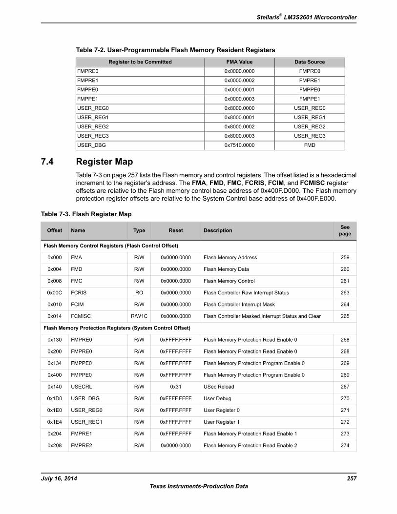
Table 7-2. User-Programmable Flash Memory Resident Registers
Data SourceFMA ValueRegister to be Committed
FMPRE00x0000.0000FMPRE0
FMPRE10x0000.0002FMPRE1
FMPPE00x0000.0001FMPPE0
FMPPE10x0000.0003FMPPE1
USER_REG00x8000.0000USER_REG0
USER_REG10x8000.0001USER_REG1
USER_REG20x8000.0002USER_REG2
USER_REG30x8000.0003USER_REG3
FMD0x7510.0000USER_DBG
7.4 Register MapTable 7-3 on page 257 lists the Flash memory and control registers. The offset listed is a hexadecimalincrement to the register's address. The FMA, FMD, FMC, FCRIS, FCIM, and FCMISC registeroffsets are relative to the Flash memory control base address of 0x400F.D000. The Flash memoryprotection register offsets are relative to the System Control base address of 0x400F.E000.
Table 7-3. Flash Register Map
SeepageDescriptionResetTypeNameOffset
Flash Memory Control Registers (Flash Control Offset)
259Flash Memory Address0x0000.0000R/WFMA0x000
260Flash Memory Data0x0000.0000R/WFMD0x004
261Flash Memory Control0x0000.0000R/WFMC0x008
263Flash Controller Raw Interrupt Status0x0000.0000ROFCRIS0x00C
264Flash Controller Interrupt Mask0x0000.0000R/WFCIM0x010
265Flash Controller Masked Interrupt Status and Clear0x0000.0000R/W1CFCMISC0x014
Flash Memory Protection Registers (System Control Offset)
268Flash Memory Protection Read Enable 00xFFFF.FFFFR/WFMPRE00x130
268Flash Memory Protection Read Enable 00xFFFF.FFFFR/WFMPRE00x200
269Flash Memory Protection Program Enable 00xFFFF.FFFFR/WFMPPE00x134
269Flash Memory Protection Program Enable 00xFFFF.FFFFR/WFMPPE00x400
267USec Reload0x31R/WUSECRL0x140
270User Debug0xFFFF.FFFER/WUSER_DBG0x1D0
271User Register 00xFFFF.FFFFR/WUSER_REG00x1E0
272User Register 10xFFFF.FFFFR/WUSER_REG10x1E4
273Flash Memory Protection Read Enable 10xFFFF.FFFFR/WFMPRE10x204
274Flash Memory Protection Read Enable 20x0000.0000R/WFMPRE20x208
257July 16, 2014Texas Instruments-Production Data
Stellaris® LM3S2601 Microcontroller
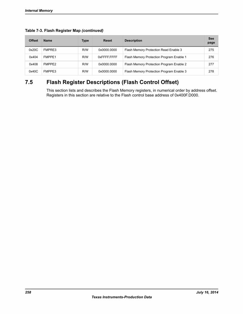
Table 7-3. Flash Register Map (continued)
SeepageDescriptionResetTypeNameOffset
275Flash Memory Protection Read Enable 30x0000.0000R/WFMPRE30x20C
276Flash Memory Protection Program Enable 10xFFFF.FFFFR/WFMPPE10x404
277Flash Memory Protection Program Enable 20x0000.0000R/WFMPPE20x408
278Flash Memory Protection Program Enable 30x0000.0000R/WFMPPE30x40C
7.5 Flash Register Descriptions (Flash Control Offset)This section lists and describes the Flash Memory registers, in numerical order by address offset.Registers in this section are relative to the Flash control base address of 0x400F.D000.
July 16, 2014258Texas Instruments-Production Data
Internal Memory
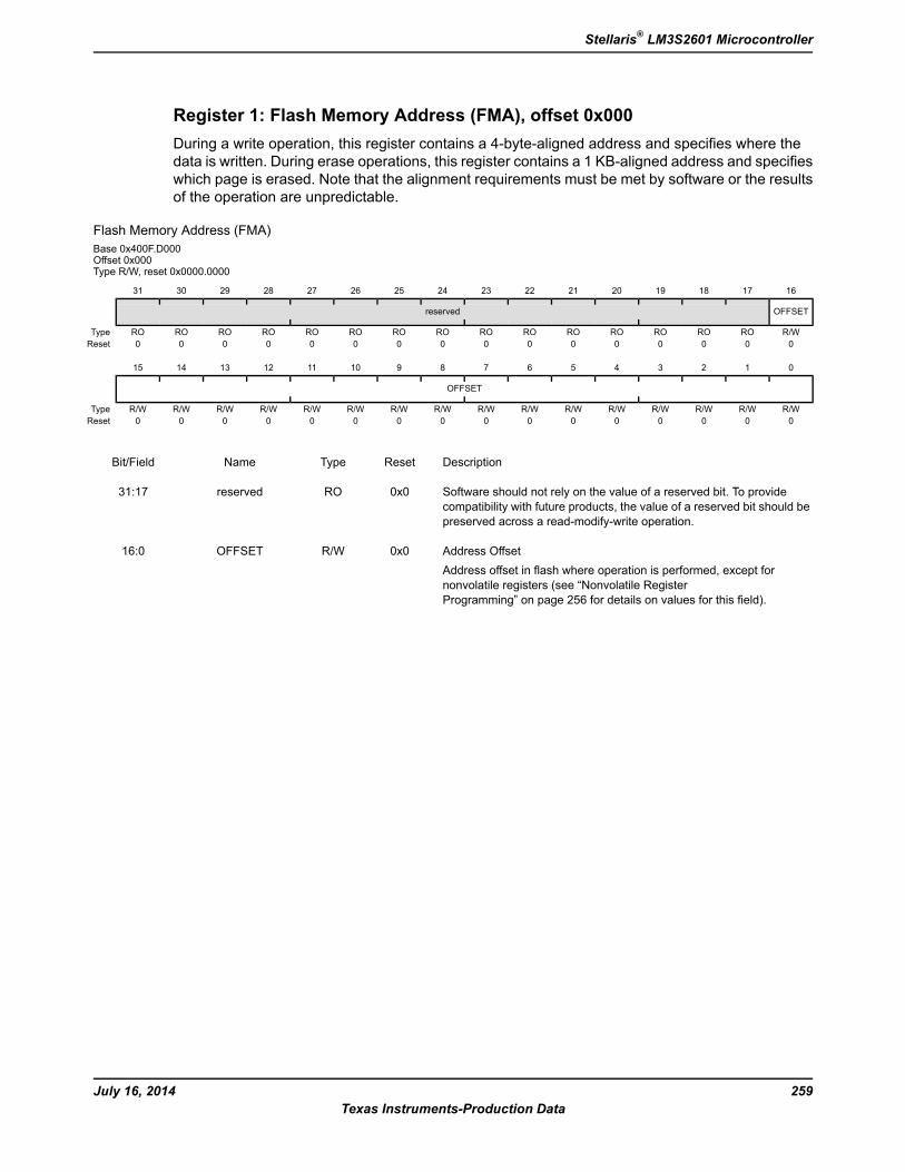
Register 1: Flash Memory Address (FMA), offset 0x000During a write operation, this register contains a 4-byte-aligned address and specifies where thedata is written. During erase operations, this register contains a 1 KB-aligned address and specifieswhich page is erased. Note that the alignment requirements must be met by software or the resultsof the operation are unpredictable.
Flash Memory Address (FMA)Base 0x400F.D000Offset 0x000Type R/W, reset 0x0000.0000
16171819202122232425262728293031
OFFSETreserved
R/WROROROROROROROROROROROROROROROType0000000000000000Reset
0123456789101112131415
OFFSET
R/WR/WR/WR/WR/WR/WR/WR/WR/WR/WR/WR/WR/WR/WR/WR/WType0000000000000000Reset
DescriptionResetTypeNameBit/Field
Software should not rely on the value of a reserved bit. To providecompatibility with future products, the value of a reserved bit should bepreserved across a read-modify-write operation.
0x0ROreserved31:17
Address OffsetAddress offset in flash where operation is performed, except fornonvolatile registers (see “Nonvolatile RegisterProgramming” on page 256 for details on values for this field).
0x0R/WOFFSET16:0
259July 16, 2014Texas Instruments-Production Data
Stellaris® LM3S2601 Microcontroller
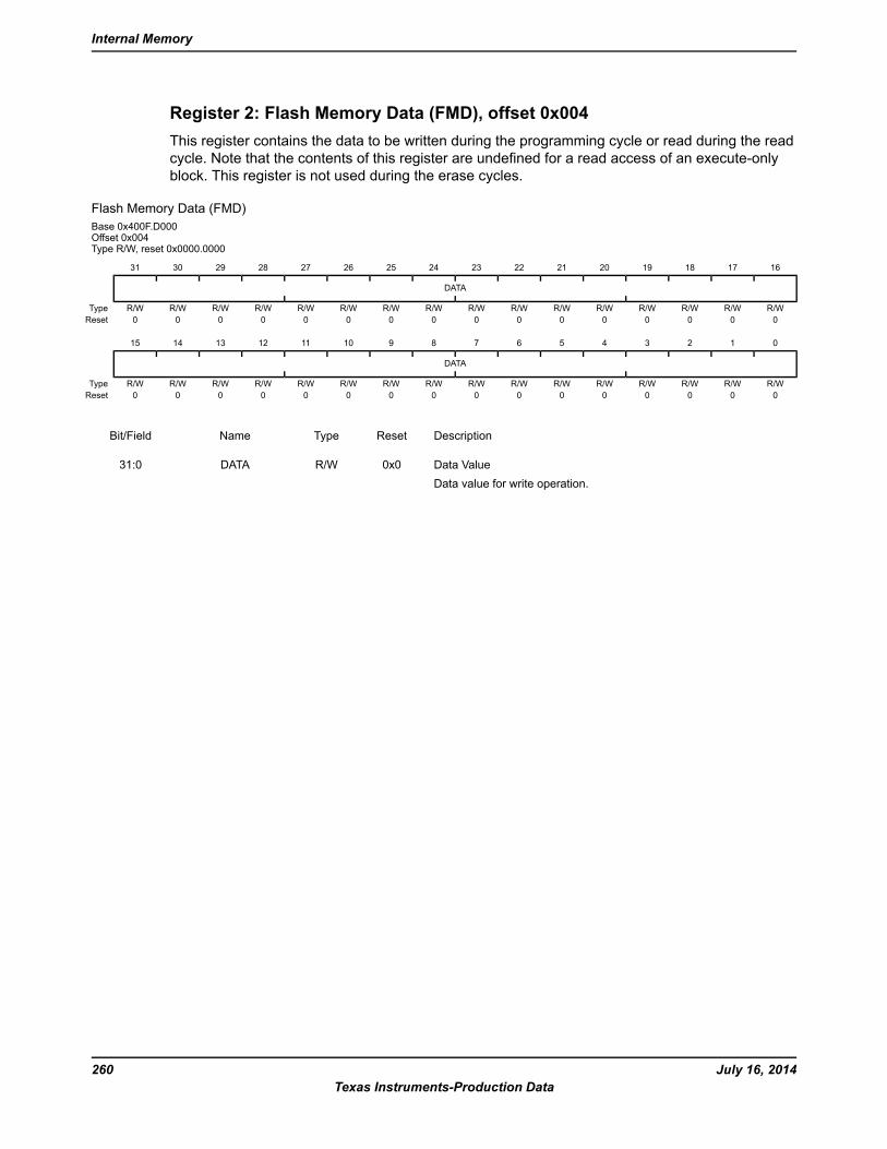
Register 2: Flash Memory Data (FMD), offset 0x004This register contains the data to be written during the programming cycle or read during the readcycle. Note that the contents of this register are undefined for a read access of an execute-onlyblock. This register is not used during the erase cycles.
Flash Memory Data (FMD)Base 0x400F.D000Offset 0x004Type R/W, reset 0x0000.0000
16171819202122232425262728293031
DATA
R/WR/WR/WR/WR/WR/WR/WR/WR/WR/WR/WR/WR/WR/WR/WR/WType0000000000000000Reset
0123456789101112131415
DATA
R/WR/WR/WR/WR/WR/WR/WR/WR/WR/WR/WR/WR/WR/WR/WR/WType0000000000000000Reset
DescriptionResetTypeNameBit/Field
Data ValueData value for write operation.
0x0R/WDATA31:0
July 16, 2014260Texas Instruments-Production Data
Internal Memory
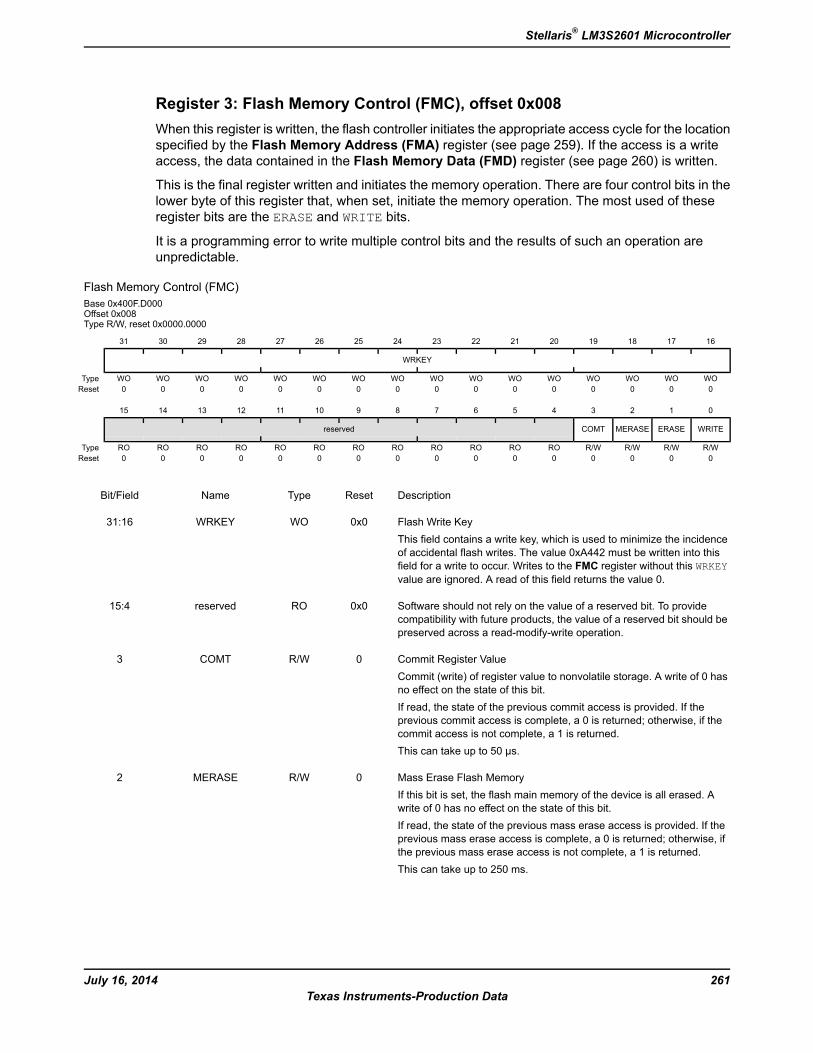
Register 3: Flash Memory Control (FMC), offset 0x008When this register is written, the flash controller initiates the appropriate access cycle for the locationspecified by the Flash Memory Address (FMA) register (see page 259). If the access is a writeaccess, the data contained in the Flash Memory Data (FMD) register (see page 260) is written.
This is the final register written and initiates the memory operation. There are four control bits in thelower byte of this register that, when set, initiate the memory operation. The most used of theseregister bits are the ERASE and WRITE bits.
It is a programming error to write multiple control bits and the results of such an operation areunpredictable.
Flash Memory Control (FMC)Base 0x400F.D000Offset 0x008Type R/W, reset 0x0000.0000
16171819202122232425262728293031
WRKEY
WOWOWOWOWOWOWOWOWOWOWOWOWOWOWOWOType0000000000000000Reset
0123456789101112131415
WRITEERASEMERASECOMTreserved
R/WR/WR/WR/WROROROROROROROROROROROROType0000000000000000Reset
DescriptionResetTypeNameBit/Field
Flash Write KeyThis field contains a write key, which is used to minimize the incidenceof accidental flash writes. The value 0xA442 must be written into thisfield for a write to occur. Writes to the FMC register without this WRKEYvalue are ignored. A read of this field returns the value 0.
0x0WOWRKEY31:16
Software should not rely on the value of a reserved bit. To providecompatibility with future products, the value of a reserved bit should bepreserved across a read-modify-write operation.
0x0ROreserved15:4
Commit Register ValueCommit (write) of register value to nonvolatile storage. A write of 0 hasno effect on the state of this bit.If read, the state of the previous commit access is provided. If theprevious commit access is complete, a 0 is returned; otherwise, if thecommit access is not complete, a 1 is returned.This can take up to 50 μs.
0R/WCOMT3
Mass Erase Flash MemoryIf this bit is set, the flash main memory of the device is all erased. Awrite of 0 has no effect on the state of this bit.If read, the state of the previous mass erase access is provided. If theprevious mass erase access is complete, a 0 is returned; otherwise, ifthe previous mass erase access is not complete, a 1 is returned.This can take up to 250 ms.
0R/WMERASE2
261July 16, 2014Texas Instruments-Production Data
Stellaris® LM3S2601 Microcontroller
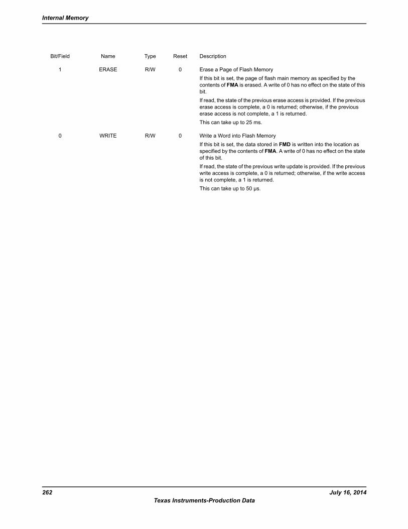
DescriptionResetTypeNameBit/Field
Erase a Page of Flash MemoryIf this bit is set, the page of flash main memory as specified by thecontents of FMA is erased. A write of 0 has no effect on the state of thisbit.If read, the state of the previous erase access is provided. If the previouserase access is complete, a 0 is returned; otherwise, if the previouserase access is not complete, a 1 is returned.This can take up to 25 ms.
0R/WERASE1
Write a Word into Flash MemoryIf this bit is set, the data stored in FMD is written into the location asspecified by the contents of FMA. A write of 0 has no effect on the stateof this bit.If read, the state of the previous write update is provided. If the previouswrite access is complete, a 0 is returned; otherwise, if the write accessis not complete, a 1 is returned.This can take up to 50 µs.
0R/WWRITE0
July 16, 2014262Texas Instruments-Production Data
Internal Memory
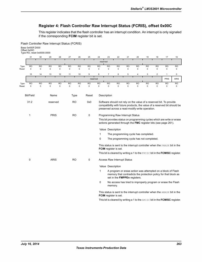
Register 4: Flash Controller Raw Interrupt Status (FCRIS), offset 0x00CThis register indicates that the flash controller has an interrupt condition. An interrupt is only signaledif the corresponding FCIM register bit is set.
Flash Controller Raw Interrupt Status (FCRIS)Base 0x400F.D000Offset 0x00CType RO, reset 0x0000.0000
16171819202122232425262728293031
reserved
ROROROROROROROROROROROROROROROROType0000000000000000Reset
0123456789101112131415
ARISPRISreserved
ROROROROROROROROROROROROROROROROType0000000000000000Reset
DescriptionResetTypeNameBit/Field
Software should not rely on the value of a reserved bit. To providecompatibility with future products, the value of a reserved bit should bepreserved across a read-modify-write operation.
0x0ROreserved31:2
Programming Raw Interrupt StatusThis bit provides status on programming cycles which are write or eraseactions generated through the FMC register bits (see page 261).
DescriptionValue
The programming cycle has completed.1
The programming cycle has not completed.0
This status is sent to the interrupt controller when the PMASK bit in theFCIM register is set.This bit is cleared by writing a 1 to the PMISC bit in the FCMISC register.
0ROPRIS1
Access Raw Interrupt Status
DescriptionValue
A program or erase action was attempted on a block of Flashmemory that contradicts the protection policy for that block asset in the FMPPEn registers.
1
No access has tried to improperly program or erase the Flashmemory.
0
This status is sent to the interrupt controller when the AMASK bit in theFCIM register is set.This bit is cleared by writing a 1 to the AMISC bit in the FCMISC register.
0ROARIS0
263July 16, 2014Texas Instruments-Production Data
Stellaris® LM3S2601 Microcontroller
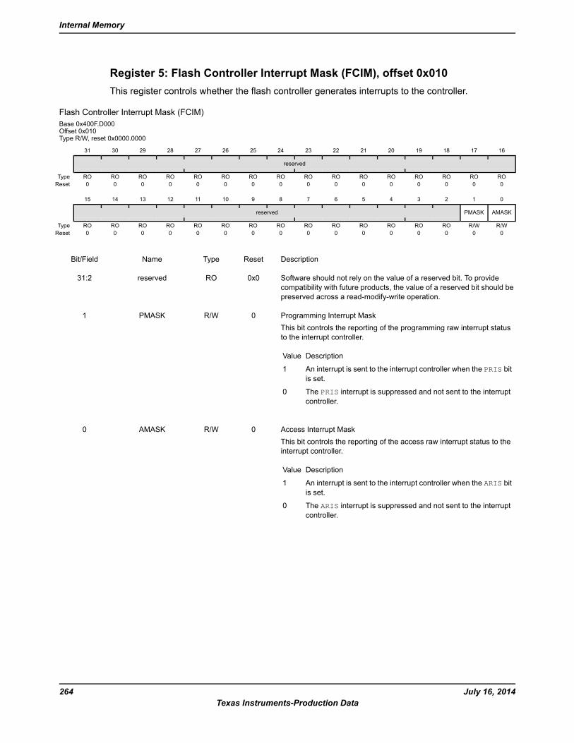
Register 5: Flash Controller Interrupt Mask (FCIM), offset 0x010This register controls whether the flash controller generates interrupts to the controller.
Flash Controller Interrupt Mask (FCIM)Base 0x400F.D000Offset 0x010Type R/W, reset 0x0000.0000
16171819202122232425262728293031
reserved
ROROROROROROROROROROROROROROROROType0000000000000000Reset
0123456789101112131415
AMASKPMASKreserved
R/WR/WROROROROROROROROROROROROROROType0000000000000000Reset
DescriptionResetTypeNameBit/Field
Software should not rely on the value of a reserved bit. To providecompatibility with future products, the value of a reserved bit should bepreserved across a read-modify-write operation.
0x0ROreserved31:2
Programming Interrupt MaskThis bit controls the reporting of the programming raw interrupt statusto the interrupt controller.
DescriptionValue
An interrupt is sent to the interrupt controller when the PRIS bitis set.
1
The PRIS interrupt is suppressed and not sent to the interruptcontroller.
0
0R/WPMASK1
Access Interrupt MaskThis bit controls the reporting of the access raw interrupt status to theinterrupt controller.
DescriptionValue
An interrupt is sent to the interrupt controller when the ARIS bitis set.
1
The ARIS interrupt is suppressed and not sent to the interruptcontroller.
0
0R/WAMASK0
July 16, 2014264Texas Instruments-Production Data
Internal Memory
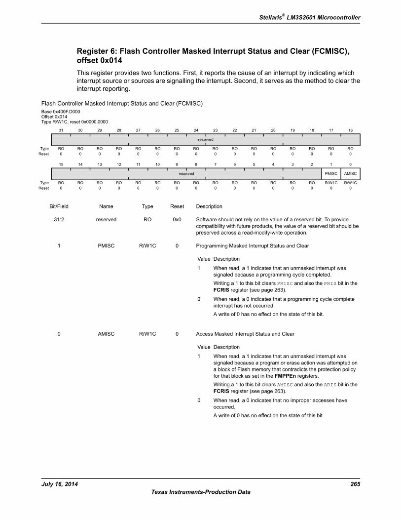
Register 6: Flash Controller Masked Interrupt Status and Clear (FCMISC),offset 0x014This register provides two functions. First, it reports the cause of an interrupt by indicating whichinterrupt source or sources are signalling the interrupt. Second, it serves as the method to clear theinterrupt reporting.
Flash Controller Masked Interrupt Status and Clear (FCMISC)Base 0x400F.D000Offset 0x014Type R/W1C, reset 0x0000.0000
16171819202122232425262728293031
reserved
ROROROROROROROROROROROROROROROROType0000000000000000Reset
0123456789101112131415
AMISCPMISCreserved
R/W1CR/W1CROROROROROROROROROROROROROROType0000000000000000Reset
DescriptionResetTypeNameBit/Field
Software should not rely on the value of a reserved bit. To providecompatibility with future products, the value of a reserved bit should bepreserved across a read-modify-write operation.
0x0ROreserved31:2
Programming Masked Interrupt Status and Clear
DescriptionValue
When read, a 1 indicates that an unmasked interrupt wassignaled because a programming cycle completed.Writing a 1 to this bit clears PMISC and also the PRIS bit in theFCRIS register (see page 263).
1
When read, a 0 indicates that a programming cycle completeinterrupt has not occurred.A write of 0 has no effect on the state of this bit.
0
0R/W1CPMISC1
Access Masked Interrupt Status and Clear
DescriptionValue
When read, a 1 indicates that an unmasked interrupt wassignaled because a program or erase action was attempted ona block of Flash memory that contradicts the protection policyfor that block as set in the FMPPEn registers.Writing a 1 to this bit clears AMISC and also the ARIS bit in theFCRIS register (see page 263).
1
When read, a 0 indicates that no improper accesses haveoccurred.A write of 0 has no effect on the state of this bit.
0
0R/W1CAMISC0
265July 16, 2014Texas Instruments-Production Data
Stellaris® LM3S2601 Microcontroller

7.6 Flash Register Descriptions (System Control Offset)The remainder of this section lists and describes the Flash Memory registers, in numerical order byaddress offset. Registers in this section are relative to the System Control base address of0x400F.E000.
July 16, 2014266Texas Instruments-Production Data
Internal Memory
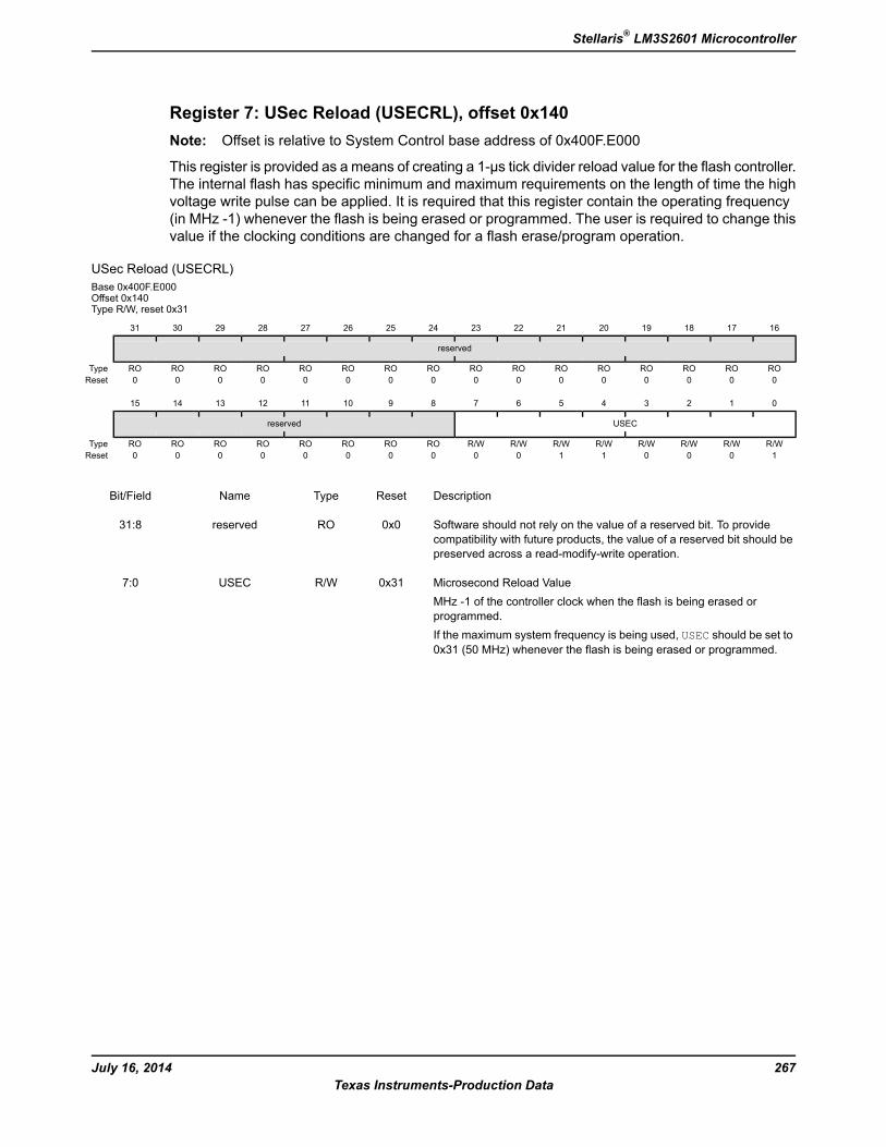
Register 7: USec Reload (USECRL), offset 0x140Note: Offset is relative to System Control base address of 0x400F.E000
This register is provided as a means of creating a 1-μs tick divider reload value for the flash controller.The internal flash has specific minimum and maximum requirements on the length of time the highvoltage write pulse can be applied. It is required that this register contain the operating frequency(in MHz -1) whenever the flash is being erased or programmed. The user is required to change thisvalue if the clocking conditions are changed for a flash erase/program operation.
USec Reload (USECRL)Base 0x400F.E000Offset 0x140Type R/W, reset 0x31
16171819202122232425262728293031
reserved
ROROROROROROROROROROROROROROROROType0000000000000000Reset
0123456789101112131415
USECreserved
R/WR/WR/WR/WR/WR/WR/WR/WROROROROROROROROType1000110000000000Reset
DescriptionResetTypeNameBit/Field
Software should not rely on the value of a reserved bit. To providecompatibility with future products, the value of a reserved bit should bepreserved across a read-modify-write operation.
0x0ROreserved31:8
Microsecond Reload ValueMHz -1 of the controller clock when the flash is being erased orprogrammed.If the maximum system frequency is being used, USEC should be set to0x31 (50 MHz) whenever the flash is being erased or programmed.
0x31R/WUSEC7:0
267July 16, 2014Texas Instruments-Production Data
Stellaris® LM3S2601 Microcontroller
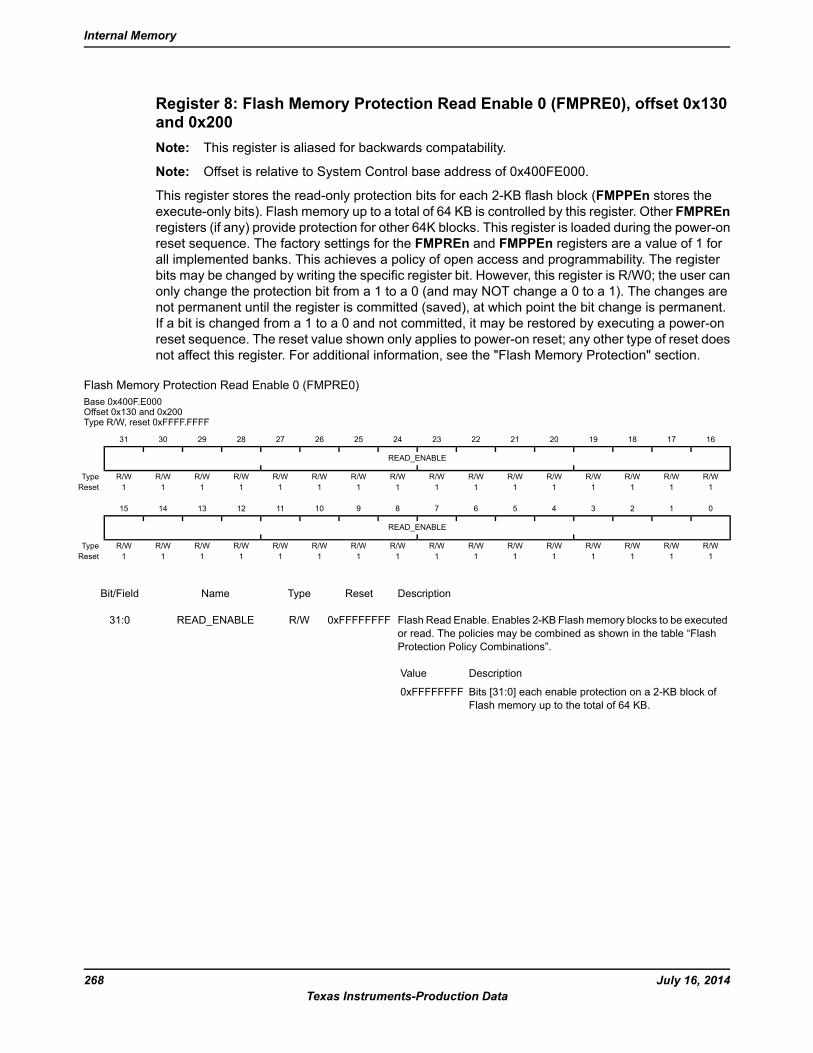
Register 8: Flash Memory Protection Read Enable 0 (FMPRE0), offset 0x130and 0x200Note: This register is aliased for backwards compatability.
Note: Offset is relative to System Control base address of 0x400FE000.
This register stores the read-only protection bits for each 2-KB flash block (FMPPEn stores theexecute-only bits). Flash memory up to a total of 64 KB is controlled by this register. Other FMPREnregisters (if any) provide protection for other 64K blocks. This register is loaded during the power-onreset sequence. The factory settings for the FMPREn and FMPPEn registers are a value of 1 forall implemented banks. This achieves a policy of open access and programmability. The registerbits may be changed by writing the specific register bit. However, this register is R/W0; the user canonly change the protection bit from a 1 to a 0 (and may NOT change a 0 to a 1). The changes arenot permanent until the register is committed (saved), at which point the bit change is permanent.If a bit is changed from a 1 to a 0 and not committed, it may be restored by executing a power-onreset sequence. The reset value shown only applies to power-on reset; any other type of reset doesnot affect this register. For additional information, see the "Flash Memory Protection" section.
Flash Memory Protection Read Enable 0 (FMPRE0)Base 0x400F.E000Offset 0x130 and 0x200Type R/W, reset 0xFFFF.FFFF
16171819202122232425262728293031
READ_ENABLE
R/WR/WR/WR/WR/WR/WR/WR/WR/WR/WR/WR/WR/WR/WR/WR/WType1111111111111111Reset
0123456789101112131415
READ_ENABLE
R/WR/WR/WR/WR/WR/WR/WR/WR/WR/WR/WR/WR/WR/WR/WR/WType1111111111111111Reset
DescriptionResetTypeNameBit/Field
Flash Read Enable. Enables 2-KB Flash memory blocks to be executedor read. The policies may be combined as shown in the table “FlashProtection Policy Combinations”.
DescriptionValue
Bits [31:0] each enable protection on a 2-KB block ofFlash memory up to the total of 64 KB.
0xFFFFFFFF
0xFFFFFFFFR/WREAD_ENABLE31:0
July 16, 2014268Texas Instruments-Production Data
Internal Memory
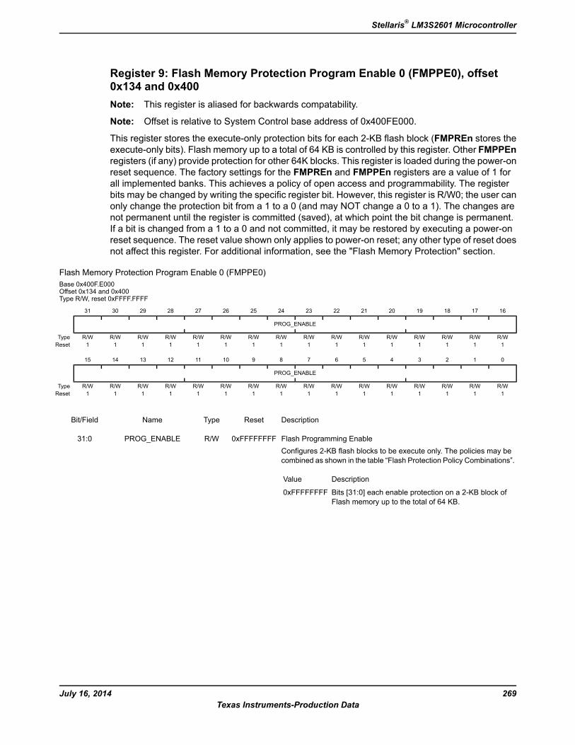
Register 9: Flash Memory Protection Program Enable 0 (FMPPE0), offset0x134 and 0x400Note: This register is aliased for backwards compatability.
Note: Offset is relative to System Control base address of 0x400FE000.
This register stores the execute-only protection bits for each 2-KB flash block (FMPREn stores theexecute-only bits). Flash memory up to a total of 64 KB is controlled by this register. Other FMPPEnregisters (if any) provide protection for other 64K blocks. This register is loaded during the power-onreset sequence. The factory settings for the FMPREn and FMPPEn registers are a value of 1 forall implemented banks. This achieves a policy of open access and programmability. The registerbits may be changed by writing the specific register bit. However, this register is R/W0; the user canonly change the protection bit from a 1 to a 0 (and may NOT change a 0 to a 1). The changes arenot permanent until the register is committed (saved), at which point the bit change is permanent.If a bit is changed from a 1 to a 0 and not committed, it may be restored by executing a power-onreset sequence. The reset value shown only applies to power-on reset; any other type of reset doesnot affect this register. For additional information, see the "Flash Memory Protection" section.
Flash Memory Protection Program Enable 0 (FMPPE0)Base 0x400F.E000Offset 0x134 and 0x400Type R/W, reset 0xFFFF.FFFF
16171819202122232425262728293031
PROG_ENABLE
R/WR/WR/WR/WR/WR/WR/WR/WR/WR/WR/WR/WR/WR/WR/WR/WType1111111111111111Reset
0123456789101112131415
PROG_ENABLE
R/WR/WR/WR/WR/WR/WR/WR/WR/WR/WR/WR/WR/WR/WR/WR/WType1111111111111111Reset
DescriptionResetTypeNameBit/Field
Flash Programming EnableConfigures 2-KB flash blocks to be execute only. The policies may becombined as shown in the table “Flash Protection Policy Combinations”.
DescriptionValue
Bits [31:0] each enable protection on a 2-KB block ofFlash memory up to the total of 64 KB.
0xFFFFFFFF
0xFFFFFFFFR/WPROG_ENABLE31:0
269July 16, 2014Texas Instruments-Production Data
Stellaris® LM3S2601 Microcontroller
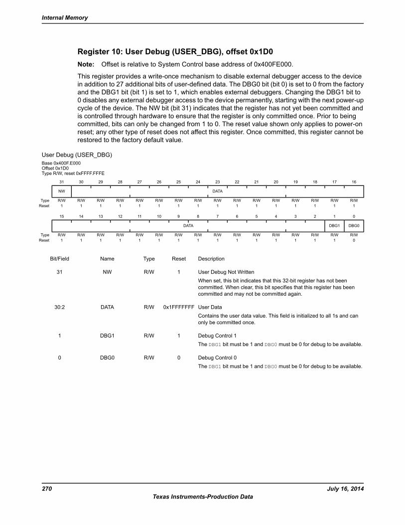
Register 10: User Debug (USER_DBG), offset 0x1D0Note: Offset is relative to System Control base address of 0x400FE000.
This register provides a write-once mechanism to disable external debugger access to the devicein addition to 27 additional bits of user-defined data. The DBG0 bit (bit 0) is set to 0 from the factoryand the DBG1 bit (bit 1) is set to 1, which enables external debuggers. Changing the DBG1 bit to0 disables any external debugger access to the device permanently, starting with the next power-upcycle of the device. The NW bit (bit 31) indicates that the register has not yet been committed andis controlled through hardware to ensure that the register is only committed once. Prior to beingcommitted, bits can only be changed from 1 to 0. The reset value shown only applies to power-onreset; any other type of reset does not affect this register. Once committed, this register cannot berestored to the factory default value.
User Debug (USER_DBG)Base 0x400F.E000Offset 0x1D0Type R/W, reset 0xFFFF.FFFE
16171819202122232425262728293031
DATANW
R/WR/WR/WR/WR/WR/WR/WR/WR/WR/WR/WR/WR/WR/WR/WR/WType1111111111111111Reset
0123456789101112131415
DBG0DBG1DATA
R/WR/WR/WR/WR/WR/WR/WR/WR/WR/WR/WR/WR/WR/WR/WR/WType0111111111111111Reset
DescriptionResetTypeNameBit/Field
User Debug Not WrittenWhen set, this bit indicates that this 32-bit register has not beencommitted. When clear, this bit specifies that this register has beencommitted and may not be committed again.
1R/WNW31
User DataContains the user data value. This field is initialized to all 1s and canonly be committed once.
0x1FFFFFFFR/WDATA30:2
Debug Control 1The DBG1 bit must be 1 and DBG0 must be 0 for debug to be available.
1R/WDBG11
Debug Control 0The DBG1 bit must be 1 and DBG0 must be 0 for debug to be available.
0R/WDBG00
July 16, 2014270Texas Instruments-Production Data
Internal Memory
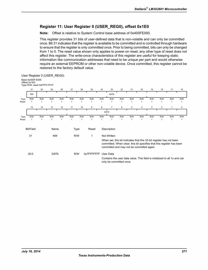
Register 11: User Register 0 (USER_REG0), offset 0x1E0Note: Offset is relative to System Control base address of 0x400FE000.
This register provides 31 bits of user-defined data that is non-volatile and can only be committedonce. Bit 31 indicates that the register is available to be committed and is controlled through hardwareto ensure that the register is only committed once. Prior to being committed, bits can only be changedfrom 1 to 0. The reset value shown only applies to power-on reset; any other type of reset does notaffect this register. The write-once characteristics of this register are useful for keeping staticinformation like communication addresses that need to be unique per part and would otherwiserequire an external EEPROM or other non-volatile device. Once committed, this register cannot berestored to the factory default value.
User Register 0 (USER_REG0)Base 0x400F.E000Offset 0x1E0Type R/W, reset 0xFFFF.FFFF
16171819202122232425262728293031
DATANW
R/WR/WR/WR/WR/WR/WR/WR/WR/WR/WR/WR/WR/WR/WR/WR/WType1111111111111111Reset
0123456789101112131415
DATA
R/WR/WR/WR/WR/WR/WR/WR/WR/WR/WR/WR/WR/WR/WR/WR/WType1111111111111111Reset
DescriptionResetTypeNameBit/Field
Not WrittenWhen set, this bit indicates that this 32-bit register has not beencommitted. When clear, this bit specifies that this register has beencommitted and may not be committed again.
1R/WNW31
User DataContains the user data value. This field is initialized to all 1s and canonly be committed once.
0x7FFFFFFFR/WDATA30:0
271July 16, 2014Texas Instruments-Production Data
Stellaris® LM3S2601 Microcontroller
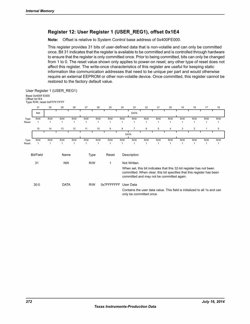
Register 12: User Register 1 (USER_REG1), offset 0x1E4Note: Offset is relative to System Control base address of 0x400FE000.
This register provides 31 bits of user-defined data that is non-volatile and can only be committedonce. Bit 31 indicates that the register is available to be committed and is controlled through hardwareto ensure that the register is only committed once. Prior to being committed, bits can only be changedfrom 1 to 0. The reset value shown only applies to power-on reset; any other type of reset does notaffect this register. The write-once characteristics of this register are useful for keeping staticinformation like communication addresses that need to be unique per part and would otherwiserequire an external EEPROM or other non-volatile device. Once committed, this register cannot berestored to the factory default value.
User Register 1 (USER_REG1)Base 0x400F.E000Offset 0x1E4Type R/W, reset 0xFFFF.FFFF
16171819202122232425262728293031
DATANW
R/WR/WR/WR/WR/WR/WR/WR/WR/WR/WR/WR/WR/WR/WR/WR/WType1111111111111111Reset
0123456789101112131415
DATA
R/WR/WR/WR/WR/WR/WR/WR/WR/WR/WR/WR/WR/WR/WR/WR/WType1111111111111111Reset
DescriptionResetTypeNameBit/Field
Not WrittenWhen set, this bit indicates that this 32-bit register has not beencommitted. When clear, this bit specifies that this register has beencommitted and may not be committed again.
1R/WNW31
User DataContains the user data value. This field is initialized to all 1s and canonly be committed once.
0x7FFFFFFFR/WDATA30:0
July 16, 2014272Texas Instruments-Production Data
Internal Memory
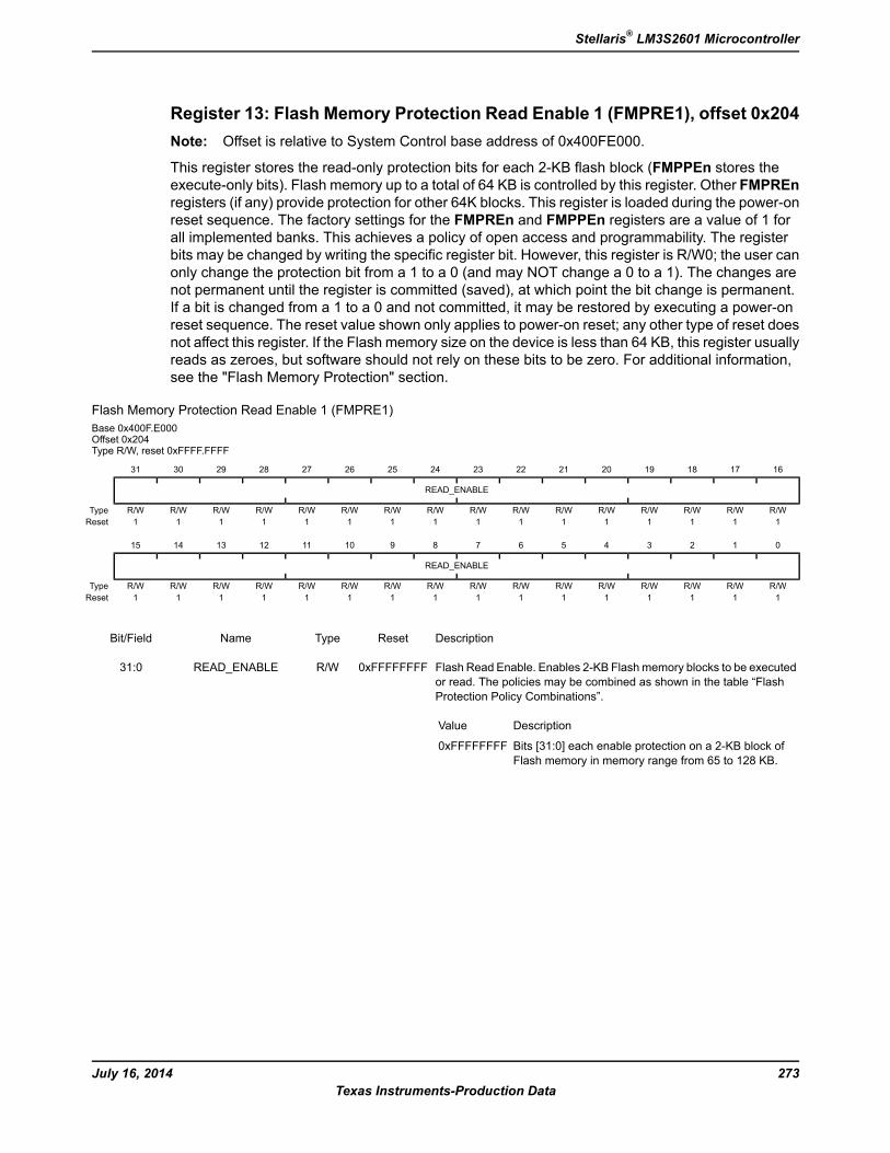
Register 13: Flash Memory Protection Read Enable 1 (FMPRE1), offset 0x204Note: Offset is relative to System Control base address of 0x400FE000.
This register stores the read-only protection bits for each 2-KB flash block (FMPPEn stores theexecute-only bits). Flash memory up to a total of 64 KB is controlled by this register. Other FMPREnregisters (if any) provide protection for other 64K blocks. This register is loaded during the power-onreset sequence. The factory settings for the FMPREn and FMPPEn registers are a value of 1 forall implemented banks. This achieves a policy of open access and programmability. The registerbits may be changed by writing the specific register bit. However, this register is R/W0; the user canonly change the protection bit from a 1 to a 0 (and may NOT change a 0 to a 1). The changes arenot permanent until the register is committed (saved), at which point the bit change is permanent.If a bit is changed from a 1 to a 0 and not committed, it may be restored by executing a power-onreset sequence. The reset value shown only applies to power-on reset; any other type of reset doesnot affect this register. If the Flash memory size on the device is less than 64 KB, this register usuallyreads as zeroes, but software should not rely on these bits to be zero. For additional information,see the "Flash Memory Protection" section.
Flash Memory Protection Read Enable 1 (FMPRE1)Base 0x400F.E000Offset 0x204Type R/W, reset 0xFFFF.FFFF
16171819202122232425262728293031
READ_ENABLE
R/WR/WR/WR/WR/WR/WR/WR/WR/WR/WR/WR/WR/WR/WR/WR/WType1111111111111111Reset
0123456789101112131415
READ_ENABLE
R/WR/WR/WR/WR/WR/WR/WR/WR/WR/WR/WR/WR/WR/WR/WR/WType1111111111111111Reset
DescriptionResetTypeNameBit/Field
Flash Read Enable. Enables 2-KB Flash memory blocks to be executedor read. The policies may be combined as shown in the table “FlashProtection Policy Combinations”.
DescriptionValue
Bits [31:0] each enable protection on a 2-KB block ofFlash memory in memory range from 65 to 128 KB.
0xFFFFFFFF
0xFFFFFFFFR/WREAD_ENABLE31:0
273July 16, 2014Texas Instruments-Production Data
Stellaris® LM3S2601 Microcontroller
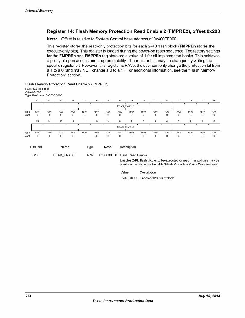
Register 14: Flash Memory Protection Read Enable 2 (FMPRE2), offset 0x208Note: Offset is relative to System Control base address of 0x400FE000.
This register stores the read-only protection bits for each 2-KB flash block (FMPPEn stores theexecute-only bits). This register is loaded during the power-on reset sequence. The factory settingsfor the FMPREn and FMPPEn registers are a value of 1 for all implemented banks. This achievesa policy of open access and programmability. The register bits may be changed by writing thespecific register bit. However, this register is R/W0; the user can only change the protection bit froma 1 to a 0 (and may NOT change a 0 to a 1). For additional information, see the "Flash MemoryProtection" section.
Flash Memory Protection Read Enable 2 (FMPRE2)Base 0x400F.E000Offset 0x208Type R/W, reset 0x0000.0000
16171819202122232425262728293031
READ_ENABLE
R/WR/WR/WR/WR/WR/WR/WR/WR/WR/WR/WR/WR/WR/WR/WR/WType0000000000000000Reset
0123456789101112131415
READ_ENABLE
R/WR/WR/WR/WR/WR/WR/WR/WR/WR/WR/WR/WR/WR/WR/WR/WType0000000000000000Reset
DescriptionResetTypeNameBit/Field
Flash Read EnableEnables 2-KB flash blocks to be executed or read. The policies may becombined as shown in the table “Flash Protection Policy Combinations”.
DescriptionValue
Enables 128 KB of flash.0x00000000
0x00000000R/WREAD_ENABLE31:0
July 16, 2014274Texas Instruments-Production Data
Internal Memory
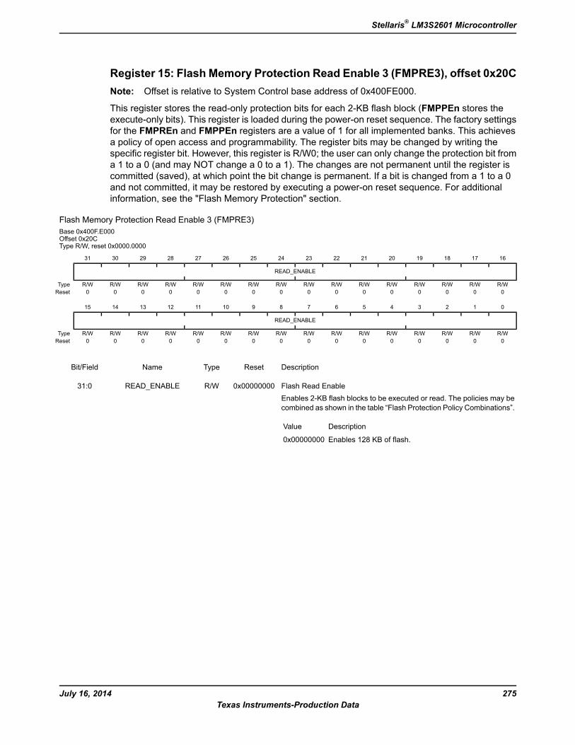
Register 15: Flash Memory Protection Read Enable 3 (FMPRE3), offset 0x20CNote: Offset is relative to System Control base address of 0x400FE000.
This register stores the read-only protection bits for each 2-KB flash block (FMPPEn stores theexecute-only bits). This register is loaded during the power-on reset sequence. The factory settingsfor the FMPREn and FMPPEn registers are a value of 1 for all implemented banks. This achievesa policy of open access and programmability. The register bits may be changed by writing thespecific register bit. However, this register is R/W0; the user can only change the protection bit froma 1 to a 0 (and may NOT change a 0 to a 1). The changes are not permanent until the register iscommitted (saved), at which point the bit change is permanent. If a bit is changed from a 1 to a 0and not committed, it may be restored by executing a power-on reset sequence. For additionalinformation, see the "Flash Memory Protection" section.
Flash Memory Protection Read Enable 3 (FMPRE3)Base 0x400F.E000Offset 0x20CType R/W, reset 0x0000.0000
16171819202122232425262728293031
READ_ENABLE
R/WR/WR/WR/WR/WR/WR/WR/WR/WR/WR/WR/WR/WR/WR/WR/WType0000000000000000Reset
0123456789101112131415
READ_ENABLE
R/WR/WR/WR/WR/WR/WR/WR/WR/WR/WR/WR/WR/WR/WR/WR/WType0000000000000000Reset
DescriptionResetTypeNameBit/Field
Flash Read EnableEnables 2-KB flash blocks to be executed or read. The policies may becombined as shown in the table “Flash Protection Policy Combinations”.
DescriptionValue
Enables 128 KB of flash.0x00000000
0x00000000R/WREAD_ENABLE31:0
275July 16, 2014Texas Instruments-Production Data
Stellaris® LM3S2601 Microcontroller
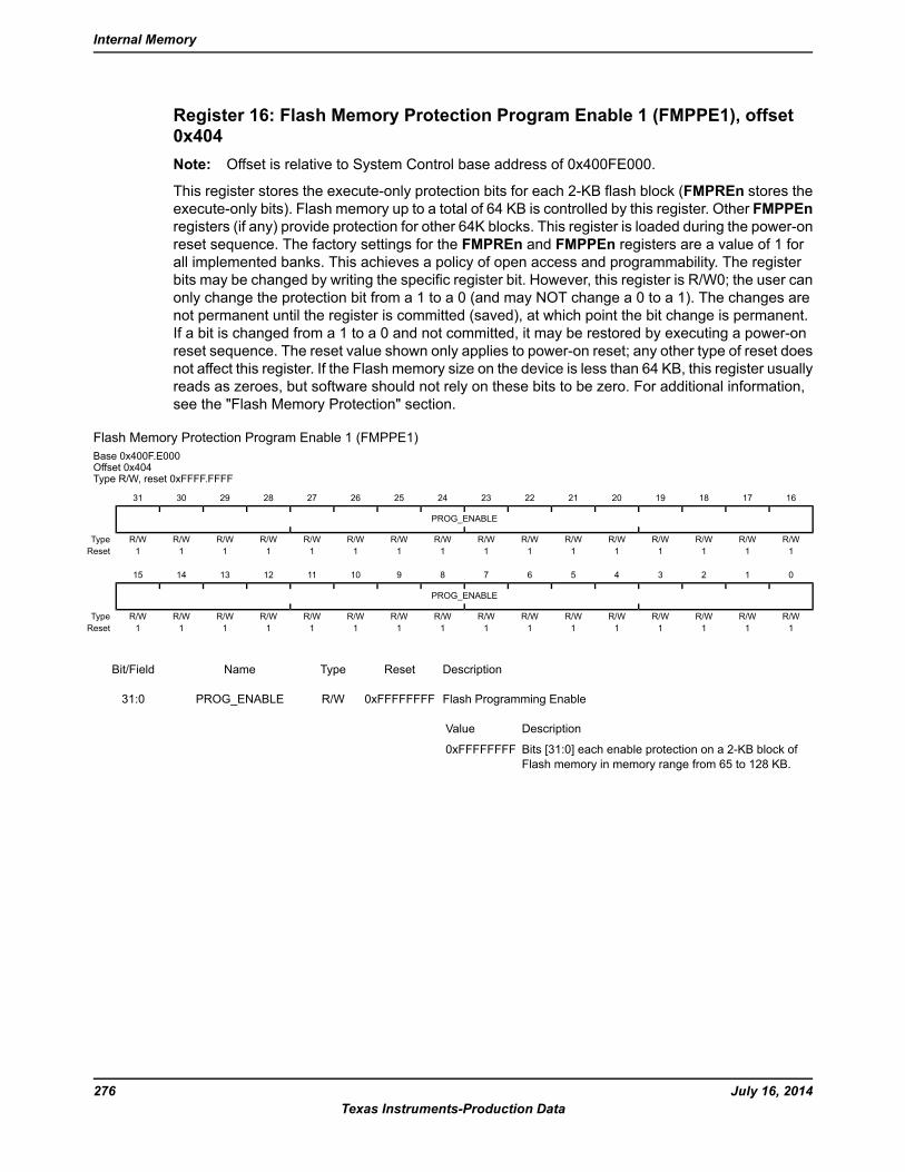
Register 16: Flash Memory Protection Program Enable 1 (FMPPE1), offset0x404Note: Offset is relative to System Control base address of 0x400FE000.
This register stores the execute-only protection bits for each 2-KB flash block (FMPREn stores theexecute-only bits). Flash memory up to a total of 64 KB is controlled by this register. Other FMPPEnregisters (if any) provide protection for other 64K blocks. This register is loaded during the power-onreset sequence. The factory settings for the FMPREn and FMPPEn registers are a value of 1 forall implemented banks. This achieves a policy of open access and programmability. The registerbits may be changed by writing the specific register bit. However, this register is R/W0; the user canonly change the protection bit from a 1 to a 0 (and may NOT change a 0 to a 1). The changes arenot permanent until the register is committed (saved), at which point the bit change is permanent.If a bit is changed from a 1 to a 0 and not committed, it may be restored by executing a power-onreset sequence. The reset value shown only applies to power-on reset; any other type of reset doesnot affect this register. If the Flash memory size on the device is less than 64 KB, this register usuallyreads as zeroes, but software should not rely on these bits to be zero. For additional information,see the "Flash Memory Protection" section.
Flash Memory Protection Program Enable 1 (FMPPE1)Base 0x400F.E000Offset 0x404Type R/W, reset 0xFFFF.FFFF
16171819202122232425262728293031
PROG_ENABLE
R/WR/WR/WR/WR/WR/WR/WR/WR/WR/WR/WR/WR/WR/WR/WR/WType1111111111111111Reset
0123456789101112131415
PROG_ENABLE
R/WR/WR/WR/WR/WR/WR/WR/WR/WR/WR/WR/WR/WR/WR/WR/WType1111111111111111Reset
DescriptionResetTypeNameBit/Field
Flash Programming Enable
DescriptionValue
Bits [31:0] each enable protection on a 2-KB block ofFlash memory in memory range from 65 to 128 KB.
0xFFFFFFFF
0xFFFFFFFFR/WPROG_ENABLE31:0
July 16, 2014276Texas Instruments-Production Data
Internal Memory
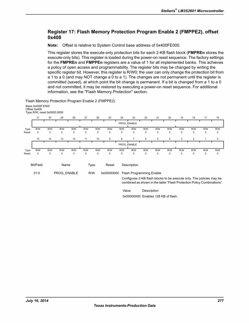
Register 17: Flash Memory Protection Program Enable 2 (FMPPE2), offset0x408Note: Offset is relative to System Control base address of 0x400FE000.
This register stores the execute-only protection bits for each 2-KB flash block (FMPREn stores theexecute-only bits). This register is loaded during the power-on reset sequence. The factory settingsfor the FMPREn and FMPPEn registers are a value of 1 for all implemented banks. This achievesa policy of open access and programmability. The register bits may be changed by writing thespecific register bit. However, this register is R/W0; the user can only change the protection bit froma 1 to a 0 (and may NOT change a 0 to a 1). The changes are not permanent until the register iscommitted (saved), at which point the bit change is permanent. If a bit is changed from a 1 to a 0and not committed, it may be restored by executing a power-on reset sequence. For additionalinformation, see the "Flash Memory Protection" section.
Flash Memory Protection Program Enable 2 (FMPPE2)Base 0x400F.E000Offset 0x408Type R/W, reset 0x0000.0000
16171819202122232425262728293031
PROG_ENABLE
R/WR/WR/WR/WR/WR/WR/WR/WR/WR/WR/WR/WR/WR/WR/WR/WType0000000000000000Reset
0123456789101112131415
PROG_ENABLE
R/WR/WR/WR/WR/WR/WR/WR/WR/WR/WR/WR/WR/WR/WR/WR/WType0000000000000000Reset
DescriptionResetTypeNameBit/Field
Flash Programming EnableConfigures 2-KB flash blocks to be execute only. The policies may becombined as shown in the table “Flash Protection Policy Combinations”.
DescriptionValue
Enables 128 KB of flash.0x00000000
0x00000000R/WPROG_ENABLE31:0
277July 16, 2014Texas Instruments-Production Data
Stellaris® LM3S2601 Microcontroller
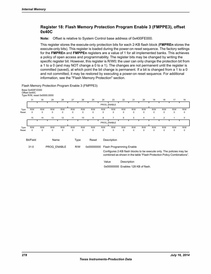
Register 18: Flash Memory Protection Program Enable 3 (FMPPE3), offset0x40CNote: Offset is relative to System Control base address of 0x400FE000.
This register stores the execute-only protection bits for each 2-KB flash block (FMPREn stores theexecute-only bits). This register is loaded during the power-on reset sequence. The factory settingsfor the FMPREn and FMPPEn registers are a value of 1 for all implemented banks. This achievesa policy of open access and programmability. The register bits may be changed by writing thespecific register bit. However, this register is R/W0; the user can only change the protection bit froma 1 to a 0 (and may NOT change a 0 to a 1). The changes are not permanent until the register iscommitted (saved), at which point the bit change is permanent. If a bit is changed from a 1 to a 0and not committed, it may be restored by executing a power-on reset sequence. For additionalinformation, see the "Flash Memory Protection" section.
Flash Memory Protection Program Enable 3 (FMPPE3)Base 0x400F.E000Offset 0x40CType R/W, reset 0x0000.0000
16171819202122232425262728293031
PROG_ENABLE
R/WR/WR/WR/WR/WR/WR/WR/WR/WR/WR/WR/WR/WR/WR/WR/WType0000000000000000Reset
0123456789101112131415
PROG_ENABLE
R/WR/WR/WR/WR/WR/WR/WR/WR/WR/WR/WR/WR/WR/WR/WR/WType0000000000000000Reset
DescriptionResetTypeNameBit/Field
Flash Programming EnableConfigures 2-KB flash blocks to be execute only. The policies may becombined as shown in the table “Flash Protection Policy Combinations”.
DescriptionValue
Enables 128 KB of flash.0x00000000
0x00000000R/WPROG_ENABLE31:0
July 16, 2014278Texas Instruments-Production Data
Internal Memory
8 General-Purpose Input/Outputs (GPIOs)The GPIO module is composed of eight physical GPIO blocks, each corresponding to an individualGPIO port (Port A, Port B, Port C, Port D, Port E, Port F, Port G, Port H). The GPIO module supports21-60 programmable input/output pins, depending on the peripherals being used.
The GPIO module has the following features:
21-60 GPIOs, depending on configuration
5-V-tolerant in input configuration
Fast toggle capable of a change every two clock cycles
Programmable control for GPIO interrupts
– Interrupt generation masking
– Edge-triggered on rising, falling, or both
– Level-sensitive on High or Low values
Bit masking in both read and write operations through address lines
Pins configured as digital inputs are Schmitt-triggered.
Programmable control for GPIO pad configuration
– Weak pull-up or pull-down resistors
– 2-mA, 4-mA, and 8-mA pad drive for digital communication; up to four pads can be configuredwith an 18-mA pad drive for high-current applications
– Slew rate control for the 8-mA drive
– Open drain enables
– Digital input enables
8.1 Signal DescriptionGPIO signals have alternate hardware functions. Table 8-4 on page 283 and Table 8-5 on page 284list the GPIO pins and the digital alternate functions. Other analog signals are 5-V tolerant and areconnected directly to their circuitry (C0-, C0+, C1-, C1+). These signals are configured by clearingthe DEN bit in theGPIO Digital Enable (GPIODEN) register. The digital alternate hardware functionsare enabled by setting the appropriate bit in the GPIO Alternate Function Select (GPIOAFSEL)and GPIODEN registers and configuring the PMCx bit field in the GPIO Port Control (GPIOPCTL)register to the numeric enoding shown in the table below. Note that each pin must be programmedindividually; no type of grouping is implied by the columns in the table.
Important: All GPIO pins are configured as GPIOs and tri-stated by default (GPIOAFSEL=0,GPIODEN=0,GPIOPDR=0,GPIOPUR=0, andGPIOPCTL=0, with the exception of thefour JTAG/SWD pins (shown in the table below). A Power-On-Reset (POR) or assertingRST puts the pins back to their default state.
279July 16, 2014Texas Instruments-Production Data
Stellaris® LM3S2601 Microcontroller
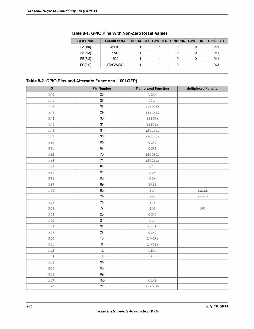
Table 8-1. GPIO Pins With Non-Zero Reset Values
GPIOPCTLGPIOPURGPIOPDRGPIODENGPIOAFSELDefault StateGPIO Pins
0x10011UART0PA[1:0]
0x10011SSI0PA[5:2]
0x10011I2C0PB[3:2]
0x31011JTAG/SWDPC[3:0]
Table 8-2. GPIO Pins and Alternate Functions (100LQFP)
Multiplexed FunctionMultiplexed FunctionPin NumberIO
U0Rx26PA0
U0Tx27PA1
SSI0Clk28PA2
SSI0Fss29PA3
SSI0Rx30PA4
SSI0Tx31PA5
I2C1SCL34PA6
I2C1SDA35PA7
CCP066PB0
CCP267PB1
I2C0SCL70PB2
I2C0SDA71PB3
C0-92PB4
C1-91PB5
C0+90PB6
TRST89PB7
SWCLKTCK80PC0
SWDIOTMS79PC1
TDI78PC2
SWOTDO77PC3
CCP525PC4
C1+24PC5
CCP323PC6
CCP422PC7
CAN0Rx10PD0
CAN0Tx11PD1
U1Rx12PD2
U1Tx13PD3
95PD4
96PD5
99PD6
CCP1100PD7
SSI1Clk72PE0
July 16, 2014280Texas Instruments-Production Data
General-Purpose Input/Outputs (GPIOs)
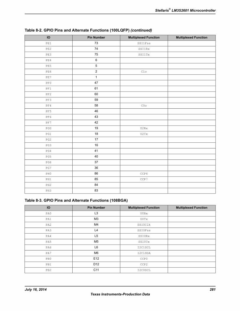
Table 8-2. GPIO Pins and Alternate Functions (100LQFP) (continued)
Multiplexed FunctionMultiplexed FunctionPin NumberIO
SSI1Fss73PE1
SSI1Rx74PE2
SSI1Tx75PE3
6PE4
5PE5
C1o2PE6
1PE7
47PF0
61PF1
60PF2
59PF3
C0o58PF4
46PF5
43PF6
42PF7
U2Rx19PG0
U2Tx18PG1
17PG2
16PG3
41PG4
40PG5
37PG6
36PG7
CCP686PH0
CCP785PH1
84PH2
83PH3
Table 8-3. GPIO Pins and Alternate Functions (108BGA)
Multiplexed FunctionMultiplexed FunctionPin NumberIO
U0RxL3PA0
U0TxM3PA1
SSI0ClkM4PA2
SSI0FssL4PA3
SSI0RxL5PA4
SSI0TxM5PA5
I2C1SCLL6PA6
I2C1SDAM6PA7
CCP0E12PB0
CCP2D12PB1
I2C0SCLC11PB2
281July 16, 2014Texas Instruments-Production Data
Stellaris® LM3S2601 Microcontroller
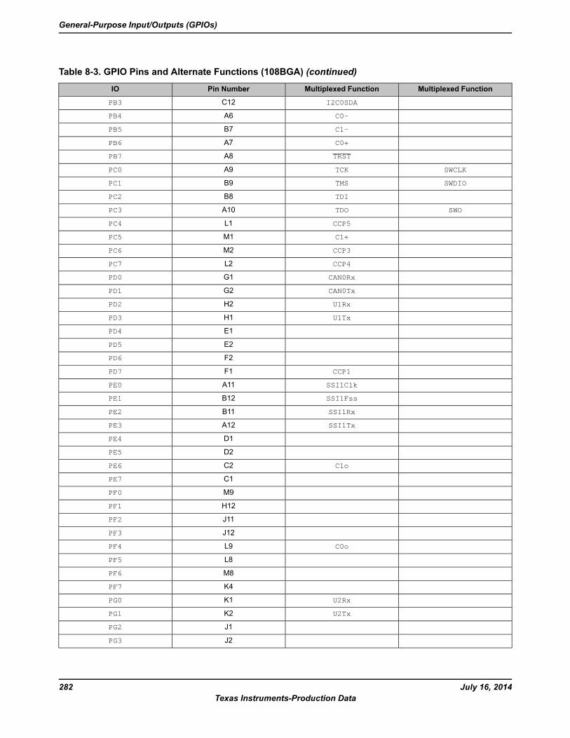
Table 8-3. GPIO Pins and Alternate Functions (108BGA) (continued)
Multiplexed FunctionMultiplexed FunctionPin NumberIO
I2C0SDAC12PB3
C0-A6PB4
C1-B7PB5
C0+A7PB6
TRSTA8PB7
SWCLKTCKA9PC0
SWDIOTMSB9PC1
TDIB8PC2
SWOTDOA10PC3
CCP5L1PC4
C1+M1PC5
CCP3M2PC6
CCP4L2PC7
CAN0RxG1PD0
CAN0TxG2PD1
U1RxH2PD2
U1TxH1PD3
E1PD4
E2PD5
F2PD6
CCP1F1PD7
SSI1ClkA11PE0
SSI1FssB12PE1
SSI1RxB11PE2
SSI1TxA12PE3
D1PE4
D2PE5
C1oC2PE6
C1PE7
M9PF0
H12PF1
J11PF2
J12PF3
C0oL9PF4
L8PF5
M8PF6
K4PF7
U2RxK1PG0
U2TxK2PG1
J1PG2
J2PG3
July 16, 2014282Texas Instruments-Production Data
General-Purpose Input/Outputs (GPIOs)
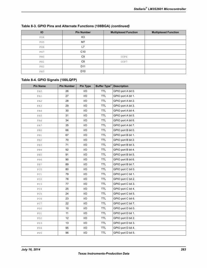
Table 8-3. GPIO Pins and Alternate Functions (108BGA) (continued)
Multiplexed FunctionMultiplexed FunctionPin NumberIO
K3PG4
M7PG5
L7PG6
C10PG7
CCP6C9PH0
CCP7C8PH1
D11PH2
D10PH3
Table 8-4. GPIO Signals (100LQFP)
DescriptionBuffer TypeaPin TypePin NumberPin Name
GPIO port A bit 0.TTLI/O26PA0
GPIO port A bit 1.TTLI/O27PA1
GPIO port A bit 2.TTLI/O28PA2
GPIO port A bit 3.TTLI/O29PA3
GPIO port A bit 4.TTLI/O30PA4
GPIO port A bit 5.TTLI/O31PA5
GPIO port A bit 6.TTLI/O34PA6
GPIO port A bit 7.TTLI/O35PA7
GPIO port B bit 0.TTLI/O66PB0
GPIO port B bit 1.TTLI/O67PB1
GPIO port B bit 2.TTLI/O70PB2
GPIO port B bit 3.TTLI/O71PB3
GPIO port B bit 4.TTLI/O92PB4
GPIO port B bit 5.TTLI/O91PB5
GPIO port B bit 6.TTLI/O90PB6
GPIO port B bit 7.TTLI/O89PB7
GPIO port C bit 0.TTLI/O80PC0
GPIO port C bit 1.TTLI/O79PC1
GPIO port C bit 2.TTLI/O78PC2
GPIO port C bit 3.TTLI/O77PC3
GPIO port C bit 4.TTLI/O25PC4
GPIO port C bit 5.TTLI/O24PC5
GPIO port C bit 6.TTLI/O23PC6
GPIO port C bit 7.TTLI/O22PC7
GPIO port D bit 0.TTLI/O10PD0
GPIO port D bit 1.TTLI/O11PD1
GPIO port D bit 2.TTLI/O12PD2
GPIO port D bit 3.TTLI/O13PD3
GPIO port D bit 4.TTLI/O95PD4
GPIO port D bit 5.TTLI/O96PD5
283July 16, 2014Texas Instruments-Production Data
Stellaris® LM3S2601 Microcontroller
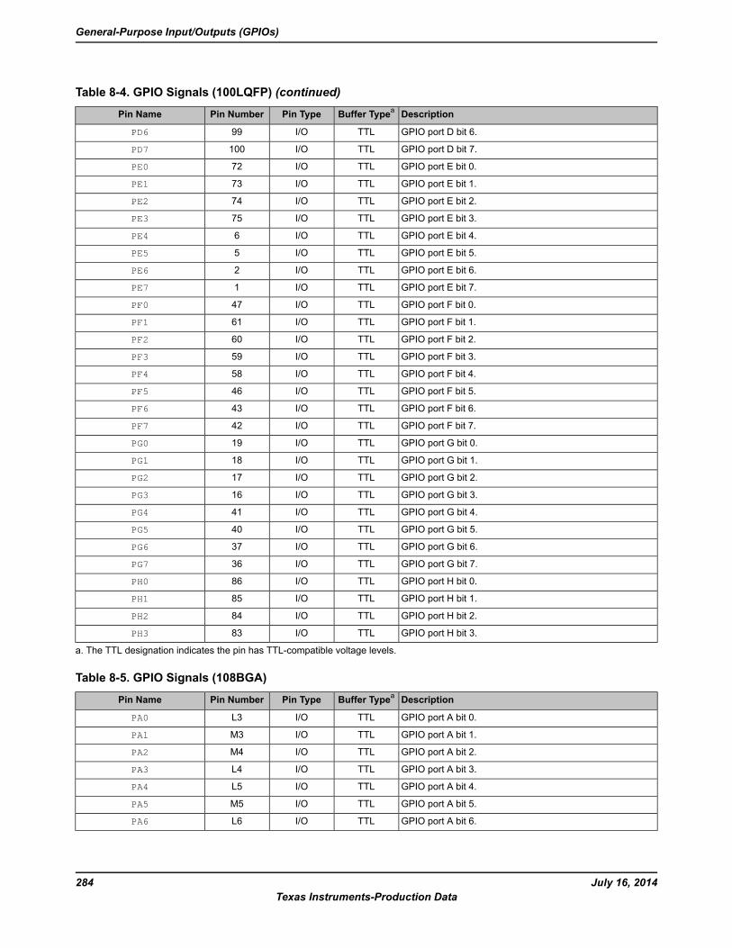
Table 8-4. GPIO Signals (100LQFP) (continued)
DescriptionBuffer TypeaPin TypePin NumberPin Name
GPIO port D bit 6.TTLI/O99PD6
GPIO port D bit 7.TTLI/O100PD7
GPIO port E bit 0.TTLI/O72PE0
GPIO port E bit 1.TTLI/O73PE1
GPIO port E bit 2.TTLI/O74PE2
GPIO port E bit 3.TTLI/O75PE3
GPIO port E bit 4.TTLI/O6PE4
GPIO port E bit 5.TTLI/O5PE5
GPIO port E bit 6.TTLI/O2PE6
GPIO port E bit 7.TTLI/O1PE7
GPIO port F bit 0.TTLI/O47PF0
GPIO port F bit 1.TTLI/O61PF1
GPIO port F bit 2.TTLI/O60PF2
GPIO port F bit 3.TTLI/O59PF3
GPIO port F bit 4.TTLI/O58PF4
GPIO port F bit 5.TTLI/O46PF5
GPIO port F bit 6.TTLI/O43PF6
GPIO port F bit 7.TTLI/O42PF7
GPIO port G bit 0.TTLI/O19PG0
GPIO port G bit 1.TTLI/O18PG1
GPIO port G bit 2.TTLI/O17PG2
GPIO port G bit 3.TTLI/O16PG3
GPIO port G bit 4.TTLI/O41PG4
GPIO port G bit 5.TTLI/O40PG5
GPIO port G bit 6.TTLI/O37PG6
GPIO port G bit 7.TTLI/O36PG7
GPIO port H bit 0.TTLI/O86PH0
GPIO port H bit 1.TTLI/O85PH1
GPIO port H bit 2.TTLI/O84PH2
GPIO port H bit 3.TTLI/O83PH3
a. The TTL designation indicates the pin has TTL-compatible voltage levels.
Table 8-5. GPIO Signals (108BGA)
DescriptionBuffer TypeaPin TypePin NumberPin Name
GPIO port A bit 0.TTLI/OL3PA0
GPIO port A bit 1.TTLI/OM3PA1
GPIO port A bit 2.TTLI/OM4PA2
GPIO port A bit 3.TTLI/OL4PA3
GPIO port A bit 4.TTLI/OL5PA4
GPIO port A bit 5.TTLI/OM5PA5
GPIO port A bit 6.TTLI/OL6PA6
July 16, 2014284Texas Instruments-Production Data
General-Purpose Input/Outputs (GPIOs)

Table 8-5. GPIO Signals (108BGA) (continued)
DescriptionBuffer TypeaPin TypePin NumberPin Name
GPIO port A bit 7.TTLI/OM6PA7
GPIO port B bit 0.TTLI/OE12PB0
GPIO port B bit 1.TTLI/OD12PB1
GPIO port B bit 2.TTLI/OC11PB2
GPIO port B bit 3.TTLI/OC12PB3
GPIO port B bit 4.TTLI/OA6PB4
GPIO port B bit 5.TTLI/OB7PB5
GPIO port B bit 6.TTLI/OA7PB6
GPIO port B bit 7.TTLI/OA8PB7
GPIO port C bit 0.TTLI/OA9PC0
GPIO port C bit 1.TTLI/OB9PC1
GPIO port C bit 2.TTLI/OB8PC2
GPIO port C bit 3.TTLI/OA10PC3
GPIO port C bit 4.TTLI/OL1PC4
GPIO port C bit 5.TTLI/OM1PC5
GPIO port C bit 6.TTLI/OM2PC6
GPIO port C bit 7.TTLI/OL2PC7
GPIO port D bit 0.TTLI/OG1PD0
GPIO port D bit 1.TTLI/OG2PD1
GPIO port D bit 2.TTLI/OH2PD2
GPIO port D bit 3.TTLI/OH1PD3
GPIO port D bit 4.TTLI/OE1PD4
GPIO port D bit 5.TTLI/OE2PD5
GPIO port D bit 6.TTLI/OF2PD6
GPIO port D bit 7.TTLI/OF1PD7
GPIO port E bit 0.TTLI/OA11PE0
GPIO port E bit 1.TTLI/OB12PE1
GPIO port E bit 2.TTLI/OB11PE2
GPIO port E bit 3.TTLI/OA12PE3
GPIO port E bit 4.TTLI/OD1PE4
GPIO port E bit 5.TTLI/OD2PE5
GPIO port E bit 6.TTLI/OC2PE6
GPIO port E bit 7.TTLI/OC1PE7
GPIO port F bit 0.TTLI/OM9PF0
GPIO port F bit 1.TTLI/OH12PF1
GPIO port F bit 2.TTLI/OJ11PF2
GPIO port F bit 3.TTLI/OJ12PF3
GPIO port F bit 4.TTLI/OL9PF4
GPIO port F bit 5.TTLI/OL8PF5
GPIO port F bit 6.TTLI/OM8PF6
GPIO port F bit 7.TTLI/OK4PF7
285July 16, 2014Texas Instruments-Production Data
Stellaris® LM3S2601 Microcontroller
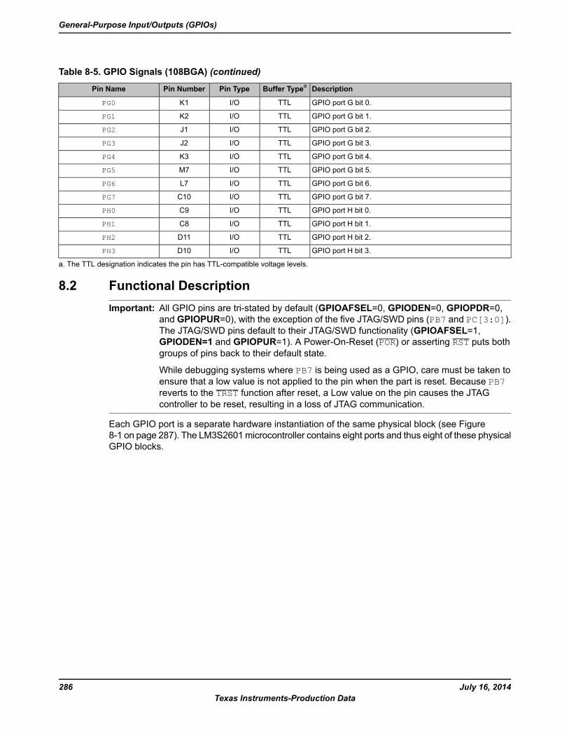
Table 8-5. GPIO Signals (108BGA) (continued)
DescriptionBuffer TypeaPin TypePin NumberPin Name
GPIO port G bit 0.TTLI/OK1PG0
GPIO port G bit 1.TTLI/OK2PG1
GPIO port G bit 2.TTLI/OJ1PG2
GPIO port G bit 3.TTLI/OJ2PG3
GPIO port G bit 4.TTLI/OK3PG4
GPIO port G bit 5.TTLI/OM7PG5
GPIO port G bit 6.TTLI/OL7PG6
GPIO port G bit 7.TTLI/OC10PG7
GPIO port H bit 0.TTLI/OC9PH0
GPIO port H bit 1.TTLI/OC8PH1
GPIO port H bit 2.TTLI/OD11PH2
GPIO port H bit 3.TTLI/OD10PH3
a. The TTL designation indicates the pin has TTL-compatible voltage levels.
8.2 Functional DescriptionImportant: All GPIO pins are tri-stated by default (GPIOAFSEL=0, GPIODEN=0, GPIOPDR=0,
and GPIOPUR=0), with the exception of the five JTAG/SWD pins (PB7 and PC[3:0]).The JTAG/SWD pins default to their JTAG/SWD functionality (GPIOAFSEL=1,GPIODEN=1 and GPIOPUR=1). A Power-On-Reset (POR) or asserting RST puts bothgroups of pins back to their default state.
While debugging systems where PB7 is being used as a GPIO, care must be taken toensure that a low value is not applied to the pin when the part is reset. Because PB7reverts to the TRST function after reset, a Low value on the pin causes the JTAGcontroller to be reset, resulting in a loss of JTAG communication.
Each GPIO port is a separate hardware instantiation of the same physical block (see Figure8-1 on page 287). The LM3S2601microcontroller contains eight ports and thus eight of these physicalGPIO blocks.
July 16, 2014286Texas Instruments-Production Data
General-Purpose Input/Outputs (GPIOs)
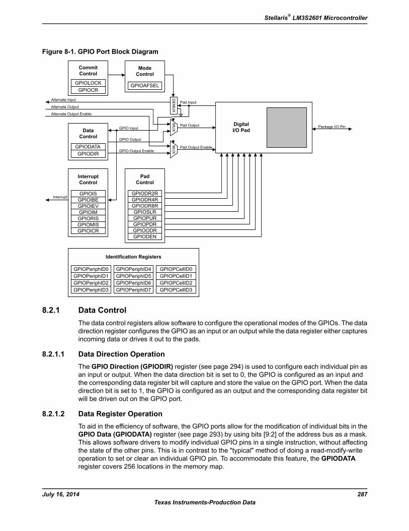
Figure 8-1. GPIO Port Block Diagram
Alternate Input
Alternate Output
Alternate Output Enable
Interrupt
GPIO Input
GPIO Output
GPIO Output Enable
Pad Output
Pad Output Enable
Package I/O Pin
GPIODATAGPIODIR
DataControl
GPIOISGPIOIBEGPIOIEVGPIOIMGPIORISGPIOMISGPIOICR
InterruptControl
GPIODR2RGPIODR4RGPIODR8RGPIOSLRGPIOPURGPIOPDRGPIOODRGPIODEN
PadControl
GPIOPeriphID0GPIOPeriphID1GPIOPeriphID2GPIOPeriphID3
GPIOPeriphID4GPIOPeriphID5GPIOPeriphID6GPIOPeriphID7
GPIOPCellID0GPIOPCellID1GPIOPCellID2GPIOPCellID3
Identification Registers
GPIOAFSEL
ModeControl
MUX
MUX
DEMUX
DigitalI/O Pad
Pad Input
GPIOLOCK
CommitControl
GPIOCR
8.2.1 Data ControlThe data control registers allow software to configure the operational modes of the GPIOs. The datadirection register configures the GPIO as an input or an output while the data register either capturesincoming data or drives it out to the pads.
8.2.1.1 Data Direction OperationThe GPIO Direction (GPIODIR) register (see page 294) is used to configure each individual pin asan input or output. When the data direction bit is set to 0, the GPIO is configured as an input andthe corresponding data register bit will capture and store the value on the GPIO port. When the datadirection bit is set to 1, the GPIO is configured as an output and the corresponding data register bitwill be driven out on the GPIO port.
8.2.1.2 Data Register OperationTo aid in the efficiency of software, the GPIO ports allow for the modification of individual bits in theGPIO Data (GPIODATA) register (see page 293) by using bits [9:2] of the address bus as a mask.This allows software drivers to modify individual GPIO pins in a single instruction, without affectingthe state of the other pins. This is in contrast to the "typical" method of doing a read-modify-writeoperation to set or clear an individual GPIO pin. To accommodate this feature, the GPIODATAregister covers 256 locations in the memory map.
287July 16, 2014Texas Instruments-Production Data
Stellaris® LM3S2601 Microcontroller
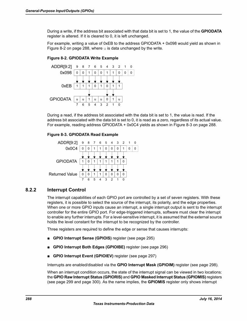
During a write, if the address bit associated with that data bit is set to 1, the value of the GPIODATAregister is altered. If it is cleared to 0, it is left unchanged.
For example, writing a value of 0xEB to the address GPIODATA + 0x098 would yield as shown inFigure 8-2 on page 288, where u is data unchanged by the write.
Figure 8-2. GPIODATA Write Example
0 10 0 1 10 0 0
u 1u u 0 1u u
9 8 7 6 5 4 3 2 1 0
1 11 0 0 11 1
7 6 5 4 3 2 1 0GPIODATA
0xEB
0x098ADDR[9:2]
0
During a read, if the address bit associated with the data bit is set to 1, the value is read. If theaddress bit associated with the data bit is set to 0, it is read as a zero, regardless of its actual value.For example, reading address GPIODATA + 0x0C4 yields as shown in Figure 8-3 on page 288.
Figure 8-3. GPIODATA Read Example
0 10 1 0 00 1 0 0
0 10 1 0 00 0
9 8 7 6 5 4 3 2 1 0
0 11 1 1 11 0
7 6 5 4 3 2 1 0Returned Value
GPIODATA
0x0C4ADDR[9:2]
8.2.2 Interrupt ControlThe interrupt capabilities of each GPIO port are controlled by a set of seven registers. With theseregisters, it is possible to select the source of the interrupt, its polarity, and the edge properties.When one or more GPIO inputs cause an interrupt, a single interrupt output is sent to the interruptcontroller for the entire GPIO port. For edge-triggered interrupts, software must clear the interruptto enable any further interrupts. For a level-sensitive interrupt, it is assumed that the external sourceholds the level constant for the interrupt to be recognized by the controller.
Three registers are required to define the edge or sense that causes interrupts:
GPIO Interrupt Sense (GPIOIS) register (see page 295)
GPIO Interrupt Both Edges (GPIOIBE) register (see page 296)
GPIO Interrupt Event (GPIOIEV) register (see page 297)
Interrupts are enabled/disabled via the GPIO Interrupt Mask (GPIOIM) register (see page 298).
When an interrupt condition occurs, the state of the interrupt signal can be viewed in two locations:theGPIORaw Interrupt Status (GPIORIS) andGPIOMasked Interrupt Status (GPIOMIS) registers(see page 299 and page 300). As the name implies, the GPIOMIS register only shows interrupt
July 16, 2014288Texas Instruments-Production Data
General-Purpose Input/Outputs (GPIOs)
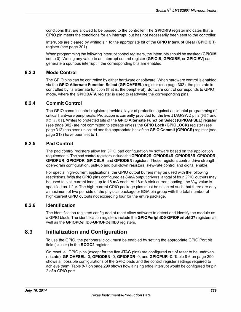
conditions that are allowed to be passed to the controller. The GPIORIS register indicates that aGPIO pin meets the conditions for an interrupt, but has not necessarily been sent to the controller.
Interrupts are cleared by writing a 1 to the appropriate bit of the GPIO Interrupt Clear (GPIOICR)register (see page 301).
When programming the following interrupt control registers, the interrupts should bemasked (GPIOIMset to 0). Writing any value to an interrupt control register (GPIOIS, GPIOIBE, or GPIOIEV) cangenerate a spurious interrupt if the corresponding bits are enabled.
8.2.3 Mode ControlThe GPIO pins can be controlled by either hardware or software. When hardware control is enabledvia the GPIO Alternate Function Select (GPIOAFSEL) register (see page 302), the pin state iscontrolled by its alternate function (that is, the peripheral). Software control corresponds to GPIOmode, where the GPIODATA register is used to read/write the corresponding pins.
8.2.4 Commit ControlThe GPIO commit control registers provide a layer of protection against accidental programming ofcritical hardware peripherals. Protection is currently provided for the five JTAG/SWD pins (PB7 andPC[3:0]). Writes to protected bits of the GPIO Alternate Function Select (GPIOAFSEL) register(see page 302) are not committed to storage unless the GPIO Lock (GPIOLOCK) register (seepage 312) has been unlocked and the appropriate bits of theGPIO Commit (GPIOCR) register (seepage 313) have been set to 1.
8.2.5 Pad ControlThe pad control registers allow for GPIO pad configuration by software based on the applicationrequirements. The pad control registers include theGPIODR2R,GPIODR4R,GPIODR8R,GPIOODR,GPIOPUR, GPIOPDR, GPIOSLR, and GPIODEN registers. These registers control drive strength,open-drain configuration, pull-up and pull-down resistors, slew-rate control and digital enable.
For special high-current applications, the GPIO output buffers may be used with the followingrestrictions. With the GPIO pins configured as 8-mA output drivers, a total of four GPIO outputs maybe used to sink current loads up to 18 mA each. At 18-mA sink current loading, the VOL value isspecified as 1.2 V. The high-current GPIO package pins must be selected such that there are onlya maximum of two per side of the physical package or BGA pin group with the total number ofhigh-current GPIO outputs not exceeding four for the entire package.
8.2.6 IdentificationThe identification registers configured at reset allow software to detect and identify the module asa GPIO block. The identification registers include theGPIOPeriphID0-GPIOPeriphID7 registers aswell as the GPIOPCellID0-GPIOPCellID3 registers.
8.3 Initialization and ConfigurationTo use the GPIO, the peripheral clock must be enabled by setting the appropriate GPIO Port bitfield (GPIOn) in the RCGC2 register.
On reset, all GPIO pins (except for the five JTAG pins) are configured out of reset to be undriven(tristate): GPIOAFSEL=0, GPIODEN=0, GPIOPDR=0, and GPIOPUR=0. Table 8-6 on page 290shows all possible configurations of the GPIO pads and the control register settings required toachieve them. Table 8-7 on page 290 shows how a rising edge interrupt would be configured for pin2 of a GPIO port.
289July 16, 2014Texas Instruments-Production Data
Stellaris® LM3S2601 Microcontroller
Table 8-6. GPIO Pad Configuration Examples
GPIO Register Bit ValueaConfiguration
SLRDR8RDR4RDR2RPDRPURDENODRDIRAFSEL
XXXX??1000Digital Input (GPIO)
??????1010Digital Output (GPIO)
????XX1110Open Drain Output(GPIO)
????XX11X1Open DrainInput/Output (I2C)
XXXX??10X1Digital Input (TimerCCP)
??????10X1Digital Output (TimerPWM)
??????10X1Digital Input/Output(SSI)
??????10X1Digital Input/Output(UART)
XXXX000000Analog Input(Comparator)
??????10X1Digital Output(Comparator)
a. X=Ignored (don’t care bit)
?=Can be either 0 or 1, depending on the configuration
Table 8-7. GPIO Interrupt Configuration Example
Pin 2 Bit ValueaDesiredInterruptEventTrigger
Register 01234567
XX0XXXXX0=edge1=level
GPIOIS
XX0XXXXX0=singleedge1=bothedges
GPIOIBE
XX1XXXXX0=Low level,or negative
edge1=High level,or positiveedge
GPIOIEV
001000000=masked1=notmasked
GPIOIM
a. X=Ignored (don’t care bit)
8.4 Register MapTable 8-8 on page 291 lists the GPIO registers. The offset listed is a hexadecimal increment to theregister’s address, relative to that GPIO port’s base address:
July 16, 2014290Texas Instruments-Production Data
General-Purpose Input/Outputs (GPIOs)
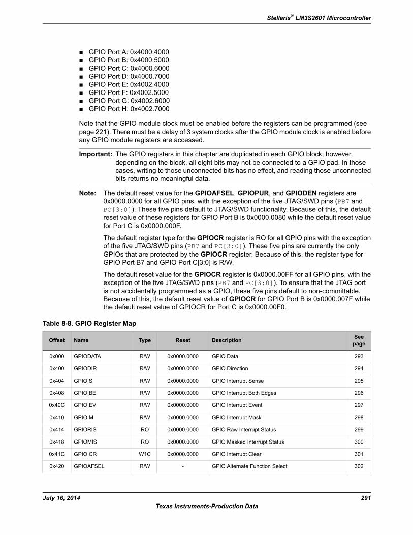
GPIO Port A: 0x4000.4000 GPIO Port B: 0x4000.5000 GPIO Port C: 0x4000.6000 GPIO Port D: 0x4000.7000 GPIO Port E: 0x4002.4000 GPIO Port F: 0x4002.5000 GPIO Port G: 0x4002.6000 GPIO Port H: 0x4002.7000
Note that the GPIO module clock must be enabled before the registers can be programmed (seepage 221). There must be a delay of 3 system clocks after the GPIOmodule clock is enabled beforeany GPIO module registers are accessed.
Important: The GPIO registers in this chapter are duplicated in each GPIO block; however,depending on the block, all eight bits may not be connected to a GPIO pad. In thosecases, writing to those unconnected bits has no effect, and reading those unconnectedbits returns no meaningful data.
Note: The default reset value for the GPIOAFSEL, GPIOPUR, and GPIODEN registers are0x0000.0000 for all GPIO pins, with the exception of the five JTAG/SWD pins (PB7 andPC[3:0]). These five pins default to JTAG/SWD functionality. Because of this, the defaultreset value of these registers for GPIO Port B is 0x0000.0080 while the default reset valuefor Port C is 0x0000.000F.
The default register type for theGPIOCR register is RO for all GPIO pins with the exceptionof the five JTAG/SWD pins (PB7 and PC[3:0]). These five pins are currently the onlyGPIOs that are protected by the GPIOCR register. Because of this, the register type forGPIO Port B7 and GPIO Port C[3:0] is R/W.
The default reset value for the GPIOCR register is 0x0000.00FF for all GPIO pins, with theexception of the five JTAG/SWD pins (PB7 and PC[3:0]). To ensure that the JTAG portis not accidentally programmed as a GPIO, these five pins default to non-committable.Because of this, the default reset value of GPIOCR for GPIO Port B is 0x0000.007F whilethe default reset value of GPIOCR for Port C is 0x0000.00F0.
Table 8-8. GPIO Register Map
SeepageDescriptionResetTypeNameOffset
293GPIO Data0x0000.0000R/WGPIODATA0x000
294GPIO Direction0x0000.0000R/WGPIODIR0x400
295GPIO Interrupt Sense0x0000.0000R/WGPIOIS0x404
296GPIO Interrupt Both Edges0x0000.0000R/WGPIOIBE0x408
297GPIO Interrupt Event0x0000.0000R/WGPIOIEV0x40C
298GPIO Interrupt Mask0x0000.0000R/WGPIOIM0x410
299GPIO Raw Interrupt Status0x0000.0000ROGPIORIS0x414
300GPIO Masked Interrupt Status0x0000.0000ROGPIOMIS0x418
301GPIO Interrupt Clear0x0000.0000W1CGPIOICR0x41C
302GPIO Alternate Function Select-R/WGPIOAFSEL0x420
291July 16, 2014Texas Instruments-Production Data
Stellaris® LM3S2601 Microcontroller
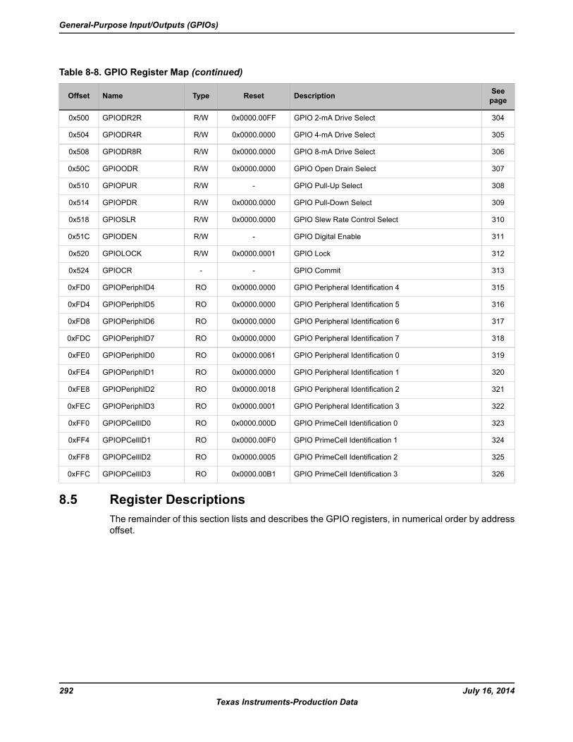
Table 8-8. GPIO Register Map (continued)
SeepageDescriptionResetTypeNameOffset
304GPIO 2-mA Drive Select0x0000.00FFR/WGPIODR2R0x500
305GPIO 4-mA Drive Select0x0000.0000R/WGPIODR4R0x504
306GPIO 8-mA Drive Select0x0000.0000R/WGPIODR8R0x508
307GPIO Open Drain Select0x0000.0000R/WGPIOODR0x50C
308GPIO Pull-Up Select-R/WGPIOPUR0x510
309GPIO Pull-Down Select0x0000.0000R/WGPIOPDR0x514
310GPIO Slew Rate Control Select0x0000.0000R/WGPIOSLR0x518
311GPIO Digital Enable-R/WGPIODEN0x51C
312GPIO Lock0x0000.0001R/WGPIOLOCK0x520
313GPIO Commit--GPIOCR0x524
315GPIO Peripheral Identification 40x0000.0000ROGPIOPeriphID40xFD0
316GPIO Peripheral Identification 50x0000.0000ROGPIOPeriphID50xFD4
317GPIO Peripheral Identification 60x0000.0000ROGPIOPeriphID60xFD8
318GPIO Peripheral Identification 70x0000.0000ROGPIOPeriphID70xFDC
319GPIO Peripheral Identification 00x0000.0061ROGPIOPeriphID00xFE0
320GPIO Peripheral Identification 10x0000.0000ROGPIOPeriphID10xFE4
321GPIO Peripheral Identification 20x0000.0018ROGPIOPeriphID20xFE8
322GPIO Peripheral Identification 30x0000.0001ROGPIOPeriphID30xFEC
323GPIO PrimeCell Identification 00x0000.000DROGPIOPCellID00xFF0
324GPIO PrimeCell Identification 10x0000.00F0ROGPIOPCellID10xFF4
325GPIO PrimeCell Identification 20x0000.0005ROGPIOPCellID20xFF8
326GPIO PrimeCell Identification 30x0000.00B1ROGPIOPCellID30xFFC
8.5 Register DescriptionsThe remainder of this section lists and describes the GPIO registers, in numerical order by addressoffset.
July 16, 2014292Texas Instruments-Production Data
General-Purpose Input/Outputs (GPIOs)
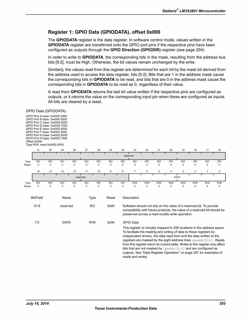
Register 1: GPIO Data (GPIODATA), offset 0x000The GPIODATA register is the data register. In software control mode, values written in theGPIODATA register are transferred onto the GPIO port pins if the respective pins have beenconfigured as outputs through the GPIO Direction (GPIODIR) register (see page 294).
In order to write to GPIODATA, the corresponding bits in the mask, resulting from the address busbits [9:2], must be High. Otherwise, the bit values remain unchanged by the write.
Similarly, the values read from this register are determined for each bit by the mask bit derived fromthe address used to access the data register, bits [9:2]. Bits that are 1 in the address mask causethe corresponding bits in GPIODATA to be read, and bits that are 0 in the address mask cause thecorresponding bits in GPIODATA to be read as 0, regardless of their value.
A read from GPIODATA returns the last bit value written if the respective pins are configured asoutputs, or it returns the value on the corresponding input pin when these are configured as inputs.All bits are cleared by a reset.
GPIO Data (GPIODATA)GPIO Port A base: 0x4000.4000GPIO Port B base: 0x4000.5000GPIO Port C base: 0x4000.6000GPIO Port D base: 0x4000.7000GPIO Port E base: 0x4002.4000GPIO Port F base: 0x4002.5000GPIO Port G base: 0x4002.6000GPIO Port H base: 0x4002.7000Offset 0x000Type R/W, reset 0x0000.0000
16171819202122232425262728293031
reserved
ROROROROROROROROROROROROROROROROType0000000000000000Reset
0123456789101112131415
DATAreserved
R/WR/WR/WR/WR/WR/WR/WR/WROROROROROROROROType0000000000000000Reset
DescriptionResetTypeNameBit/Field
Software should not rely on the value of a reserved bit. To providecompatibility with future products, the value of a reserved bit should bepreserved across a read-modify-write operation.
0x00ROreserved31:8
GPIO DataThis register is virtually mapped to 256 locations in the address space.To facilitate the reading and writing of data to these registers byindependent drivers, the data read from and the data written to theregisters are masked by the eight address lines ipaddr[9:2]. Readsfrom this register return its current state. Writes to this register only affectbits that are not masked by ipaddr[9:2] and are configured asoutputs. See “Data Register Operation” on page 287 for examples ofreads and writes.
0x00R/WDATA7:0
293July 16, 2014Texas Instruments-Production Data
Stellaris® LM3S2601 Microcontroller
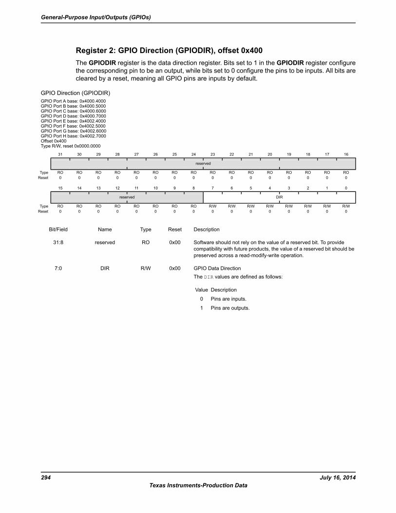
Register 2: GPIO Direction (GPIODIR), offset 0x400The GPIODIR register is the data direction register. Bits set to 1 in the GPIODIR register configurethe corresponding pin to be an output, while bits set to 0 configure the pins to be inputs. All bits arecleared by a reset, meaning all GPIO pins are inputs by default.
GPIO Direction (GPIODIR)GPIO Port A base: 0x4000.4000GPIO Port B base: 0x4000.5000GPIO Port C base: 0x4000.6000GPIO Port D base: 0x4000.7000GPIO Port E base: 0x4002.4000GPIO Port F base: 0x4002.5000GPIO Port G base: 0x4002.6000GPIO Port H base: 0x4002.7000Offset 0x400Type R/W, reset 0x0000.0000
16171819202122232425262728293031
reserved
ROROROROROROROROROROROROROROROROType0000000000000000Reset
0123456789101112131415
DIRreserved
R/WR/WR/WR/WR/WR/WR/WR/WROROROROROROROROType0000000000000000Reset
DescriptionResetTypeNameBit/Field
Software should not rely on the value of a reserved bit. To providecompatibility with future products, the value of a reserved bit should bepreserved across a read-modify-write operation.
0x00ROreserved31:8
GPIO Data DirectionThe DIR values are defined as follows:
DescriptionValue
Pins are inputs.0
Pins are outputs.1
0x00R/WDIR7:0
July 16, 2014294Texas Instruments-Production Data
General-Purpose Input/Outputs (GPIOs)
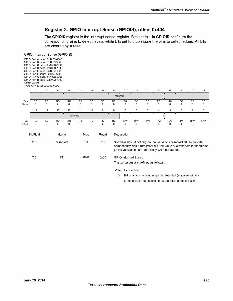
Register 3: GPIO Interrupt Sense (GPIOIS), offset 0x404The GPIOIS register is the interrupt sense register. Bits set to 1 in GPIOIS configure thecorresponding pins to detect levels, while bits set to 0 configure the pins to detect edges. All bitsare cleared by a reset.
GPIO Interrupt Sense (GPIOIS)GPIO Port A base: 0x4000.4000GPIO Port B base: 0x4000.5000GPIO Port C base: 0x4000.6000GPIO Port D base: 0x4000.7000GPIO Port E base: 0x4002.4000GPIO Port F base: 0x4002.5000GPIO Port G base: 0x4002.6000GPIO Port H base: 0x4002.7000Offset 0x404Type R/W, reset 0x0000.0000
16171819202122232425262728293031
reserved
ROROROROROROROROROROROROROROROROType0000000000000000Reset
0123456789101112131415
ISreserved
R/WR/WR/WR/WR/WR/WR/WR/WROROROROROROROROType0000000000000000Reset
DescriptionResetTypeNameBit/Field
Software should not rely on the value of a reserved bit. To providecompatibility with future products, the value of a reserved bit should bepreserved across a read-modify-write operation.
0x00ROreserved31:8
GPIO Interrupt SenseThe IS values are defined as follows:
DescriptionValue
Edge on corresponding pin is detected (edge-sensitive).0
Level on corresponding pin is detected (level-sensitive).1
0x00R/WIS7:0
295July 16, 2014Texas Instruments-Production Data
Stellaris® LM3S2601 Microcontroller
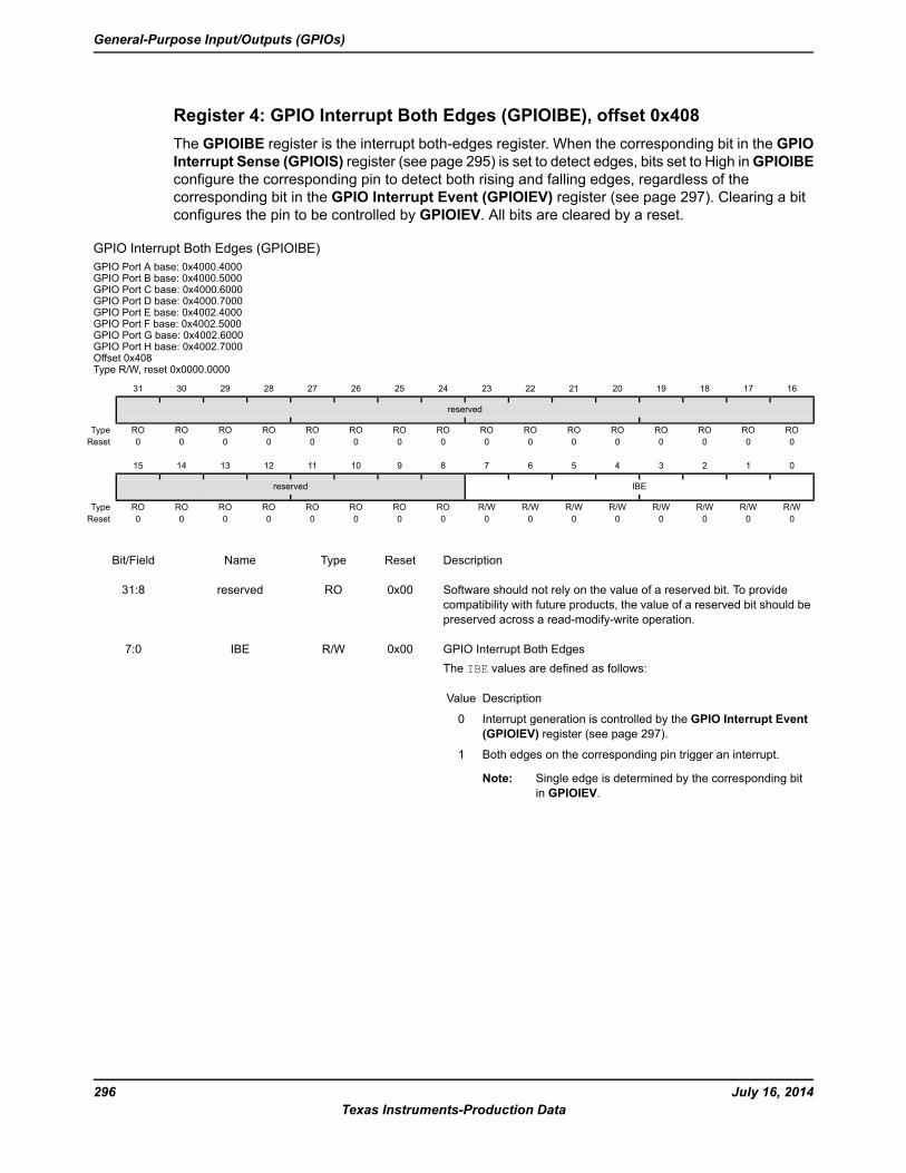
Register 4: GPIO Interrupt Both Edges (GPIOIBE), offset 0x408The GPIOIBE register is the interrupt both-edges register. When the corresponding bit in the GPIOInterrupt Sense (GPIOIS) register (see page 295) is set to detect edges, bits set to High inGPIOIBEconfigure the corresponding pin to detect both rising and falling edges, regardless of thecorresponding bit in the GPIO Interrupt Event (GPIOIEV) register (see page 297). Clearing a bitconfigures the pin to be controlled by GPIOIEV. All bits are cleared by a reset.
GPIO Interrupt Both Edges (GPIOIBE)GPIO Port A base: 0x4000.4000GPIO Port B base: 0x4000.5000GPIO Port C base: 0x4000.6000GPIO Port D base: 0x4000.7000GPIO Port E base: 0x4002.4000GPIO Port F base: 0x4002.5000GPIO Port G base: 0x4002.6000GPIO Port H base: 0x4002.7000Offset 0x408Type R/W, reset 0x0000.0000
16171819202122232425262728293031
reserved
ROROROROROROROROROROROROROROROROType0000000000000000Reset
0123456789101112131415
IBEreserved
R/WR/WR/WR/WR/WR/WR/WR/WROROROROROROROROType0000000000000000Reset
DescriptionResetTypeNameBit/Field
Software should not rely on the value of a reserved bit. To providecompatibility with future products, the value of a reserved bit should bepreserved across a read-modify-write operation.
0x00ROreserved31:8
GPIO Interrupt Both EdgesThe IBE values are defined as follows:
DescriptionValue
Interrupt generation is controlled by the GPIO Interrupt Event(GPIOIEV) register (see page 297).
0
Both edges on the corresponding pin trigger an interrupt.1
Note: Single edge is determined by the corresponding bitin GPIOIEV.
0x00R/WIBE7:0
July 16, 2014296Texas Instruments-Production Data
General-Purpose Input/Outputs (GPIOs)
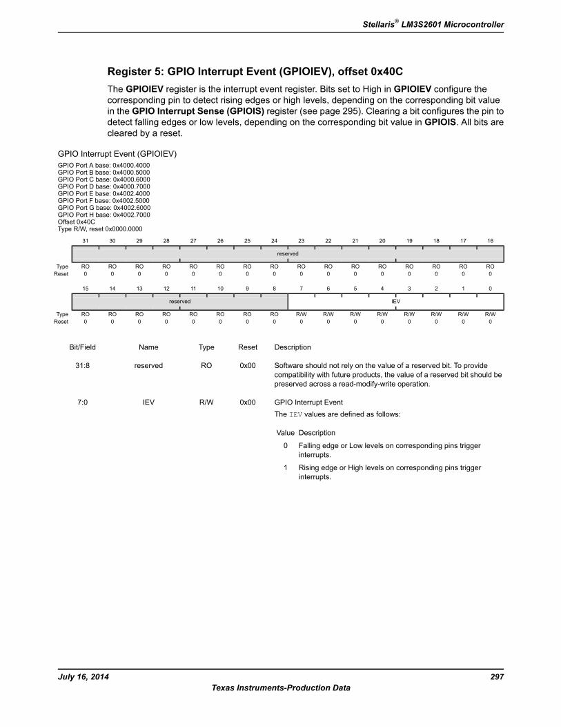
Register 5: GPIO Interrupt Event (GPIOIEV), offset 0x40CThe GPIOIEV register is the interrupt event register. Bits set to High in GPIOIEV configure thecorresponding pin to detect rising edges or high levels, depending on the corresponding bit valuein the GPIO Interrupt Sense (GPIOIS) register (see page 295). Clearing a bit configures the pin todetect falling edges or low levels, depending on the corresponding bit value in GPIOIS. All bits arecleared by a reset.
GPIO Interrupt Event (GPIOIEV)GPIO Port A base: 0x4000.4000GPIO Port B base: 0x4000.5000GPIO Port C base: 0x4000.6000GPIO Port D base: 0x4000.7000GPIO Port E base: 0x4002.4000GPIO Port F base: 0x4002.5000GPIO Port G base: 0x4002.6000GPIO Port H base: 0x4002.7000Offset 0x40CType R/W, reset 0x0000.0000
16171819202122232425262728293031
reserved
ROROROROROROROROROROROROROROROROType0000000000000000Reset
0123456789101112131415
IEVreserved
R/WR/WR/WR/WR/WR/WR/WR/WROROROROROROROROType0000000000000000Reset
DescriptionResetTypeNameBit/Field
Software should not rely on the value of a reserved bit. To providecompatibility with future products, the value of a reserved bit should bepreserved across a read-modify-write operation.
0x00ROreserved31:8
GPIO Interrupt EventThe IEV values are defined as follows:
DescriptionValue
Falling edge or Low levels on corresponding pins triggerinterrupts.
0
Rising edge or High levels on corresponding pins triggerinterrupts.
1
0x00R/WIEV7:0
297July 16, 2014Texas Instruments-Production Data
Stellaris® LM3S2601 Microcontroller
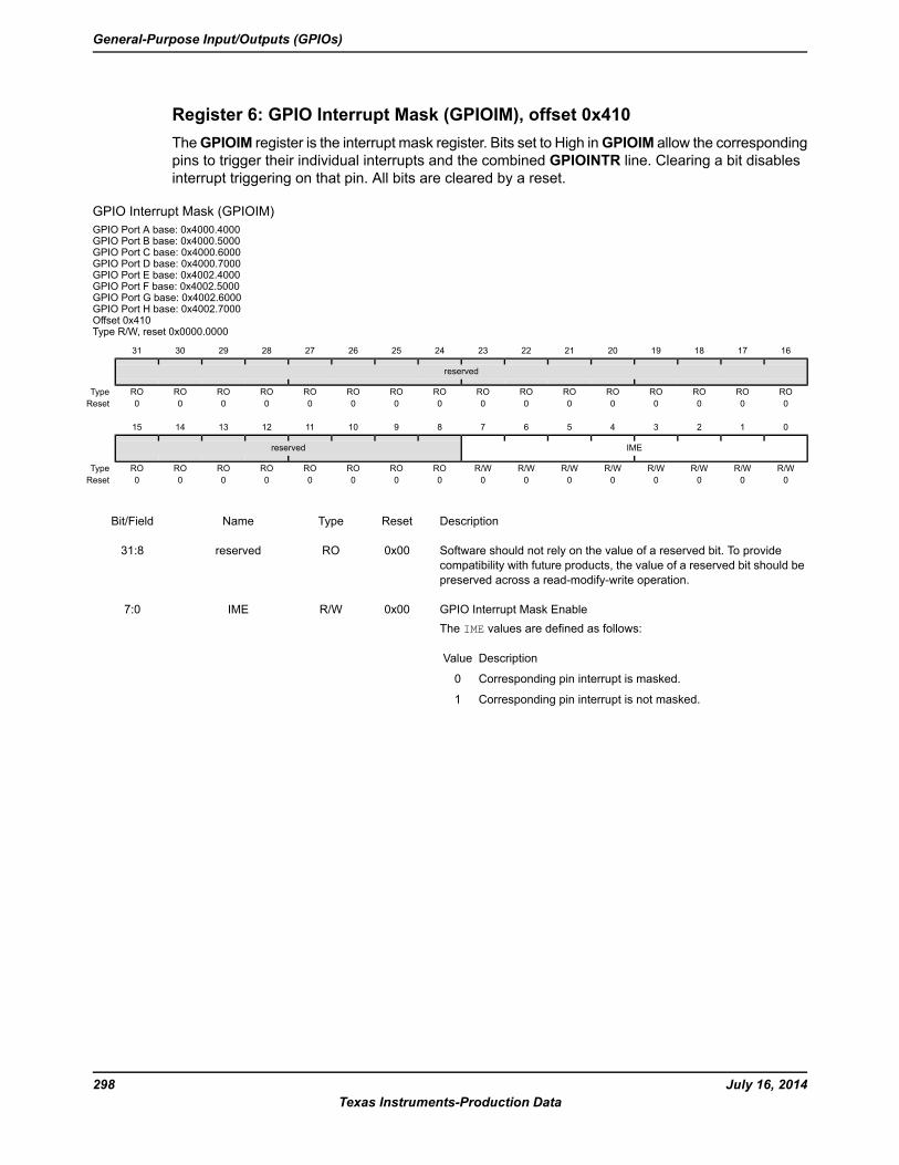
Register 6: GPIO Interrupt Mask (GPIOIM), offset 0x410TheGPIOIM register is the interrupt mask register. Bits set to High inGPIOIM allow the correspondingpins to trigger their individual interrupts and the combined GPIOINTR line. Clearing a bit disablesinterrupt triggering on that pin. All bits are cleared by a reset.
GPIO Interrupt Mask (GPIOIM)GPIO Port A base: 0x4000.4000GPIO Port B base: 0x4000.5000GPIO Port C base: 0x4000.6000GPIO Port D base: 0x4000.7000GPIO Port E base: 0x4002.4000GPIO Port F base: 0x4002.5000GPIO Port G base: 0x4002.6000GPIO Port H base: 0x4002.7000Offset 0x410Type R/W, reset 0x0000.0000
16171819202122232425262728293031
reserved
ROROROROROROROROROROROROROROROROType0000000000000000Reset
0123456789101112131415
IMEreserved
R/WR/WR/WR/WR/WR/WR/WR/WROROROROROROROROType0000000000000000Reset
DescriptionResetTypeNameBit/Field
Software should not rely on the value of a reserved bit. To providecompatibility with future products, the value of a reserved bit should bepreserved across a read-modify-write operation.
0x00ROreserved31:8
GPIO Interrupt Mask EnableThe IME values are defined as follows:
DescriptionValue
Corresponding pin interrupt is masked.0
Corresponding pin interrupt is not masked.1
0x00R/WIME7:0
July 16, 2014298Texas Instruments-Production Data
General-Purpose Input/Outputs (GPIOs)

Register 7: GPIO Raw Interrupt Status (GPIORIS), offset 0x414The GPIORIS register is the raw interrupt status register. Bits read High in GPIORIS reflect thestatus of interrupt trigger conditions detected (raw, prior to masking), indicating that all therequirements have been met, before they are finally allowed to trigger by the GPIO Interrupt Mask(GPIOIM) register (see page 298). Bits read as zero indicate that corresponding input pins have notinitiated an interrupt. All bits are cleared by a reset.
GPIO Raw Interrupt Status (GPIORIS)GPIO Port A base: 0x4000.4000GPIO Port B base: 0x4000.5000GPIO Port C base: 0x4000.6000GPIO Port D base: 0x4000.7000GPIO Port E base: 0x4002.4000GPIO Port F base: 0x4002.5000GPIO Port G base: 0x4002.6000GPIO Port H base: 0x4002.7000Offset 0x414Type RO, reset 0x0000.0000
16171819202122232425262728293031
reserved
ROROROROROROROROROROROROROROROROType0000000000000000Reset
0123456789101112131415
RISreserved
ROROROROROROROROROROROROROROROROType0000000000000000Reset
DescriptionResetTypeNameBit/Field
Software should not rely on the value of a reserved bit. To providecompatibility with future products, the value of a reserved bit should bepreserved across a read-modify-write operation.
0x00ROreserved31:8
GPIO Interrupt Raw StatusReflects the status of interrupt trigger condition detection on pins (raw,prior to masking).The RIS values are defined as follows:
DescriptionValue
Corresponding pin interrupt requirements not met.0
Corresponding pin interrupt has met requirements.1
0x00RORIS7:0
299July 16, 2014Texas Instruments-Production Data
Stellaris® LM3S2601 Microcontroller
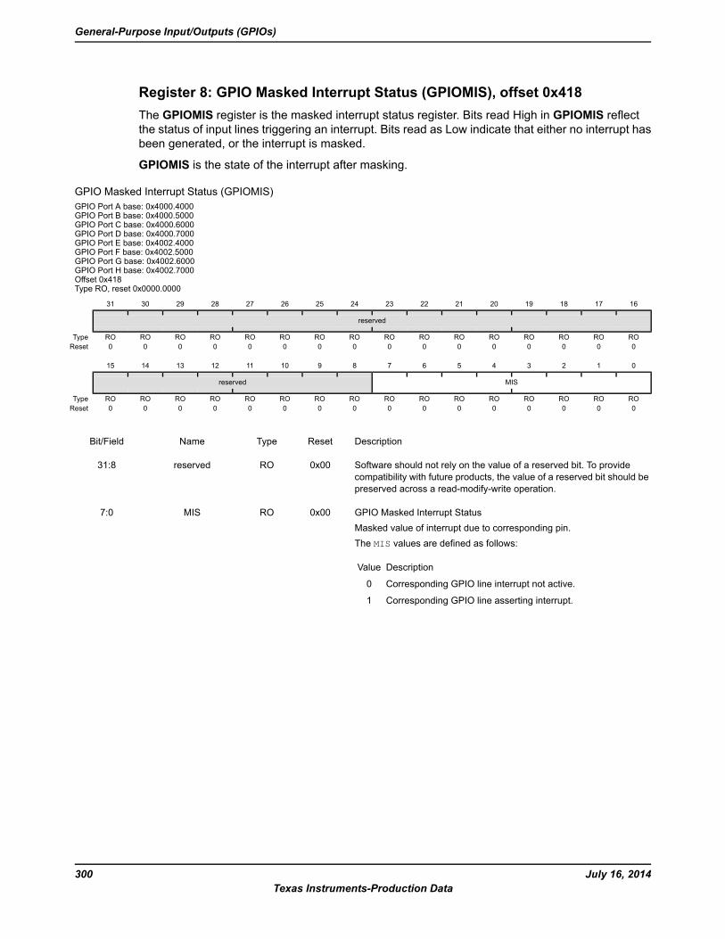
Register 8: GPIO Masked Interrupt Status (GPIOMIS), offset 0x418The GPIOMIS register is the masked interrupt status register. Bits read High in GPIOMIS reflectthe status of input lines triggering an interrupt. Bits read as Low indicate that either no interrupt hasbeen generated, or the interrupt is masked.
GPIOMIS is the state of the interrupt after masking.
GPIO Masked Interrupt Status (GPIOMIS)GPIO Port A base: 0x4000.4000GPIO Port B base: 0x4000.5000GPIO Port C base: 0x4000.6000GPIO Port D base: 0x4000.7000GPIO Port E base: 0x4002.4000GPIO Port F base: 0x4002.5000GPIO Port G base: 0x4002.6000GPIO Port H base: 0x4002.7000Offset 0x418Type RO, reset 0x0000.0000
16171819202122232425262728293031
reserved
ROROROROROROROROROROROROROROROROType0000000000000000Reset
0123456789101112131415
MISreserved
ROROROROROROROROROROROROROROROROType0000000000000000Reset
DescriptionResetTypeNameBit/Field
Software should not rely on the value of a reserved bit. To providecompatibility with future products, the value of a reserved bit should bepreserved across a read-modify-write operation.
0x00ROreserved31:8
GPIO Masked Interrupt StatusMasked value of interrupt due to corresponding pin.The MIS values are defined as follows:
DescriptionValue
Corresponding GPIO line interrupt not active.0
Corresponding GPIO line asserting interrupt.1
0x00ROMIS7:0
July 16, 2014300Texas Instruments-Production Data
General-Purpose Input/Outputs (GPIOs)
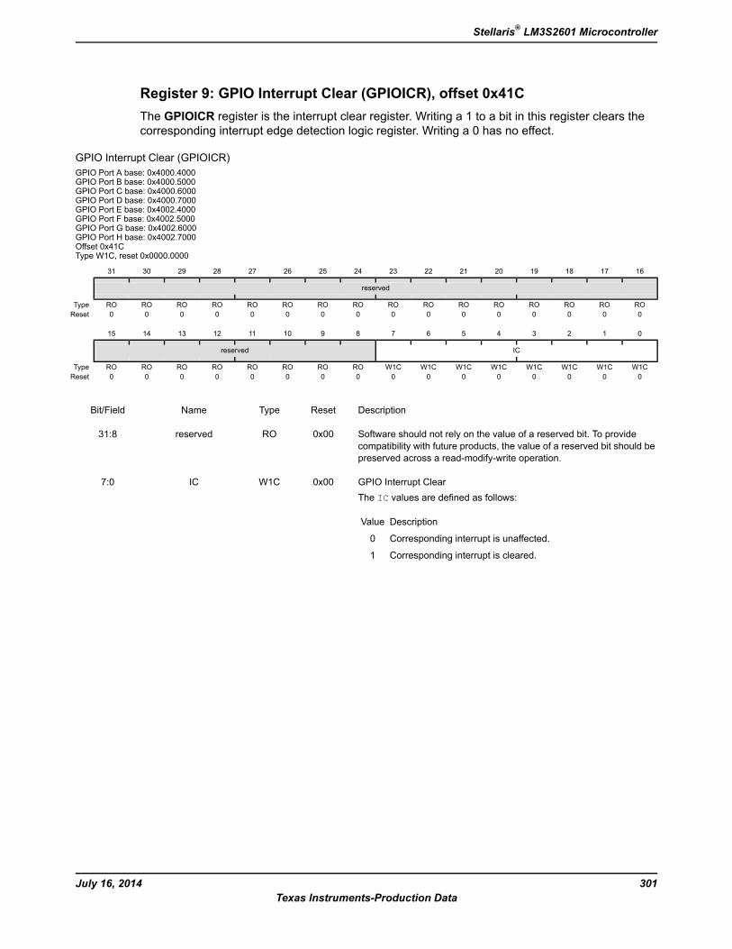
Register 9: GPIO Interrupt Clear (GPIOICR), offset 0x41CThe GPIOICR register is the interrupt clear register. Writing a 1 to a bit in this register clears thecorresponding interrupt edge detection logic register. Writing a 0 has no effect.
GPIO Interrupt Clear (GPIOICR)GPIO Port A base: 0x4000.4000GPIO Port B base: 0x4000.5000GPIO Port C base: 0x4000.6000GPIO Port D base: 0x4000.7000GPIO Port E base: 0x4002.4000GPIO Port F base: 0x4002.5000GPIO Port G base: 0x4002.6000GPIO Port H base: 0x4002.7000Offset 0x41CType W1C, reset 0x0000.0000
16171819202122232425262728293031
reserved
ROROROROROROROROROROROROROROROROType0000000000000000Reset
0123456789101112131415
ICreserved
W1CW1CW1CW1CW1CW1CW1CW1CROROROROROROROROType0000000000000000Reset
DescriptionResetTypeNameBit/Field
Software should not rely on the value of a reserved bit. To providecompatibility with future products, the value of a reserved bit should bepreserved across a read-modify-write operation.
0x00ROreserved31:8
GPIO Interrupt ClearThe IC values are defined as follows:
DescriptionValue
Corresponding interrupt is unaffected.0
Corresponding interrupt is cleared.1
0x00W1CIC7:0
301July 16, 2014Texas Instruments-Production Data
Stellaris® LM3S2601 Microcontroller
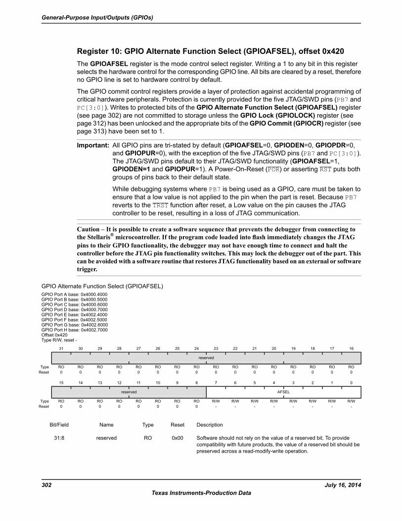
Register 10: GPIO Alternate Function Select (GPIOAFSEL), offset 0x420The GPIOAFSEL register is the mode control select register. Writing a 1 to any bit in this registerselects the hardware control for the corresponding GPIO line. All bits are cleared by a reset, thereforeno GPIO line is set to hardware control by default.
The GPIO commit control registers provide a layer of protection against accidental programming ofcritical hardware peripherals. Protection is currently provided for the five JTAG/SWD pins (PB7 andPC[3:0]). Writes to protected bits of the GPIO Alternate Function Select (GPIOAFSEL) register(see page 302) are not committed to storage unless the GPIO Lock (GPIOLOCK) register (seepage 312) has been unlocked and the appropriate bits of theGPIO Commit (GPIOCR) register (seepage 313) have been set to 1.
Important: All GPIO pins are tri-stated by default (GPIOAFSEL=0, GPIODEN=0, GPIOPDR=0,and GPIOPUR=0), with the exception of the five JTAG/SWD pins (PB7 and PC[3:0]).The JTAG/SWD pins default to their JTAG/SWD functionality (GPIOAFSEL=1,GPIODEN=1 and GPIOPUR=1). A Power-On-Reset (POR) or asserting RST puts bothgroups of pins back to their default state.
While debugging systems where PB7 is being used as a GPIO, care must be taken toensure that a low value is not applied to the pin when the part is reset. Because PB7reverts to the TRST function after reset, a Low value on the pin causes the JTAGcontroller to be reset, resulting in a loss of JTAG communication.
Caution – It is possible to create a software sequence that prevents the debugger from connecting tothe Stellaris® microcontroller. If the program code loaded into flash immediately changes the JTAGpins to their GPIO functionality, the debugger may not have enough time to connect and halt thecontroller before the JTAG pin functionality switches. This may lock the debugger out of the part. Thiscan be avoidedwith a software routine that restores JTAG functionality based on an external or softwaretrigger.
GPIO Alternate Function Select (GPIOAFSEL)GPIO Port A base: 0x4000.4000GPIO Port B base: 0x4000.5000GPIO Port C base: 0x4000.6000GPIO Port D base: 0x4000.7000GPIO Port E base: 0x4002.4000GPIO Port F base: 0x4002.5000GPIO Port G base: 0x4002.6000GPIO Port H base: 0x4002.7000Offset 0x420Type R/W, reset -
16171819202122232425262728293031
reserved
ROROROROROROROROROROROROROROROROType0000000000000000Reset
0123456789101112131415
AFSELreserved
R/WR/WR/WR/WR/WR/WR/WR/WROROROROROROROROType--------00000000Reset
DescriptionResetTypeNameBit/Field
Software should not rely on the value of a reserved bit. To providecompatibility with future products, the value of a reserved bit should bepreserved across a read-modify-write operation.
0x00ROreserved31:8
July 16, 2014302Texas Instruments-Production Data
General-Purpose Input/Outputs (GPIOs)
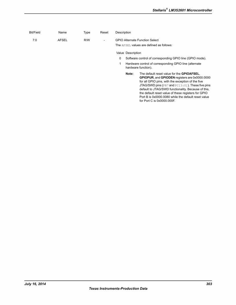
DescriptionResetTypeNameBit/Field
GPIO Alternate Function SelectThe AFSEL values are defined as follows:
DescriptionValue
Software control of corresponding GPIO line (GPIO mode).0
Hardware control of corresponding GPIO line (alternatehardware function).
1
Note: The default reset value for the GPIOAFSEL,GPIOPUR, andGPIODEN registers are 0x0000.0000for all GPIO pins, with the exception of the fiveJTAG/SWD pins (PB7 and PC[3:0]). These five pinsdefault to JTAG/SWD functionality. Because of this,the default reset value of these registers for GPIOPort B is 0x0000.0080 while the default reset valuefor Port C is 0x0000.000F.
-R/WAFSEL7:0
303July 16, 2014Texas Instruments-Production Data
Stellaris® LM3S2601 Microcontroller

Register 11: GPIO 2-mA Drive Select (GPIODR2R), offset 0x500The GPIODR2R register is the 2-mA drive control register. It allows for each GPIO signal in the portto be individually configured without affecting the other pads. When writing a DRV2 bit for a GPIOsignal, the corresponding DRV4 bit in the GPIODR4R register and the DRV8 bit in the GPIODR8Rregister are automatically cleared by hardware.
GPIO 2-mA Drive Select (GPIODR2R)GPIO Port A base: 0x4000.4000GPIO Port B base: 0x4000.5000GPIO Port C base: 0x4000.6000GPIO Port D base: 0x4000.7000GPIO Port E base: 0x4002.4000GPIO Port F base: 0x4002.5000GPIO Port G base: 0x4002.6000GPIO Port H base: 0x4002.7000Offset 0x500Type R/W, reset 0x0000.00FF
16171819202122232425262728293031
reserved
ROROROROROROROROROROROROROROROROType0000000000000000Reset
0123456789101112131415
DRV2reserved
R/WR/WR/WR/WR/WR/WR/WR/WROROROROROROROROType1111111100000000Reset
DescriptionResetTypeNameBit/Field
Software should not rely on the value of a reserved bit. To providecompatibility with future products, the value of a reserved bit should bepreserved across a read-modify-write operation.
0x00ROreserved31:8
Output Pad 2-mA Drive EnableA write of 1 to either GPIODR4[n] or GPIODR8[n] clears thecorresponding 2-mA enable bit. The change is effective on the secondclock cycle after the write.
0xFFR/WDRV27:0
July 16, 2014304Texas Instruments-Production Data
General-Purpose Input/Outputs (GPIOs)
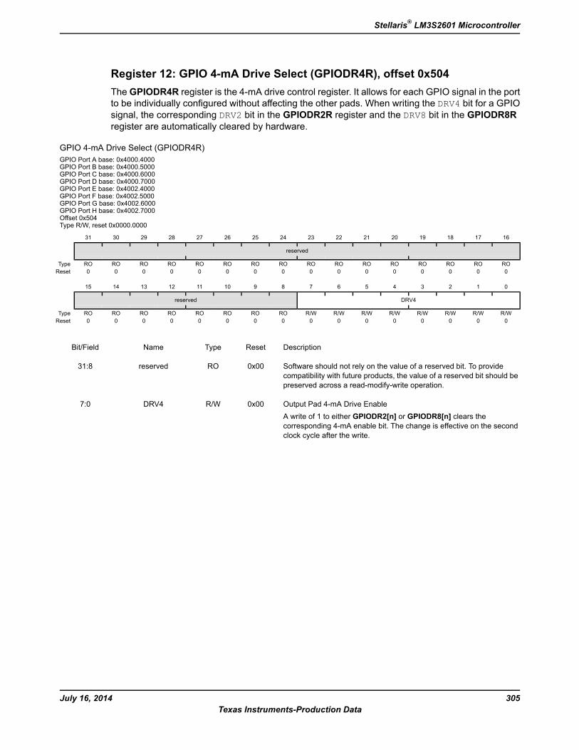
Register 12: GPIO 4-mA Drive Select (GPIODR4R), offset 0x504The GPIODR4R register is the 4-mA drive control register. It allows for each GPIO signal in the portto be individually configured without affecting the other pads. When writing the DRV4 bit for a GPIOsignal, the corresponding DRV2 bit in the GPIODR2R register and the DRV8 bit in the GPIODR8Rregister are automatically cleared by hardware.
GPIO 4-mA Drive Select (GPIODR4R)GPIO Port A base: 0x4000.4000GPIO Port B base: 0x4000.5000GPIO Port C base: 0x4000.6000GPIO Port D base: 0x4000.7000GPIO Port E base: 0x4002.4000GPIO Port F base: 0x4002.5000GPIO Port G base: 0x4002.6000GPIO Port H base: 0x4002.7000Offset 0x504Type R/W, reset 0x0000.0000
16171819202122232425262728293031
reserved
ROROROROROROROROROROROROROROROROType0000000000000000Reset
0123456789101112131415
DRV4reserved
R/WR/WR/WR/WR/WR/WR/WR/WROROROROROROROROType0000000000000000Reset
DescriptionResetTypeNameBit/Field
Software should not rely on the value of a reserved bit. To providecompatibility with future products, the value of a reserved bit should bepreserved across a read-modify-write operation.
0x00ROreserved31:8
Output Pad 4-mA Drive EnableA write of 1 to either GPIODR2[n] or GPIODR8[n] clears thecorresponding 4-mA enable bit. The change is effective on the secondclock cycle after the write.
0x00R/WDRV47:0
305July 16, 2014Texas Instruments-Production Data
Stellaris® LM3S2601 Microcontroller
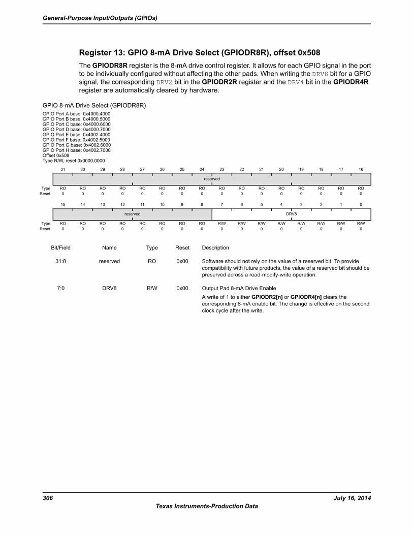
Register 13: GPIO 8-mA Drive Select (GPIODR8R), offset 0x508The GPIODR8R register is the 8-mA drive control register. It allows for each GPIO signal in the portto be individually configured without affecting the other pads. When writing the DRV8 bit for a GPIOsignal, the corresponding DRV2 bit in the GPIODR2R register and the DRV4 bit in the GPIODR4Rregister are automatically cleared by hardware.
GPIO 8-mA Drive Select (GPIODR8R)GPIO Port A base: 0x4000.4000GPIO Port B base: 0x4000.5000GPIO Port C base: 0x4000.6000GPIO Port D base: 0x4000.7000GPIO Port E base: 0x4002.4000GPIO Port F base: 0x4002.5000GPIO Port G base: 0x4002.6000GPIO Port H base: 0x4002.7000Offset 0x508Type R/W, reset 0x0000.0000
16171819202122232425262728293031
reserved
ROROROROROROROROROROROROROROROROType0000000000000000Reset
0123456789101112131415
DRV8reserved
R/WR/WR/WR/WR/WR/WR/WR/WROROROROROROROROType0000000000000000Reset
DescriptionResetTypeNameBit/Field
Software should not rely on the value of a reserved bit. To providecompatibility with future products, the value of a reserved bit should bepreserved across a read-modify-write operation.
0x00ROreserved31:8
Output Pad 8-mA Drive EnableA write of 1 to either GPIODR2[n] or GPIODR4[n] clears thecorresponding 8-mA enable bit. The change is effective on the secondclock cycle after the write.
0x00R/WDRV87:0
July 16, 2014306Texas Instruments-Production Data
General-Purpose Input/Outputs (GPIOs)
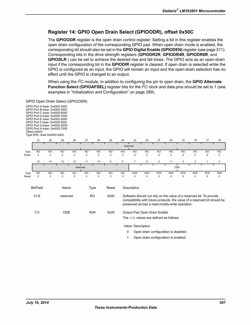
Register 14: GPIO Open Drain Select (GPIOODR), offset 0x50CThe GPIOODR register is the open drain control register. Setting a bit in this register enables theopen drain configuration of the corresponding GPIO pad. When open drain mode is enabled, thecorresponding bit should also be set in theGPIODigital Enable (GPIODEN) register (see page 311).Corresponding bits in the drive strength registers (GPIODR2R, GPIODR4R, GPIODR8R, andGPIOSLR ) can be set to achieve the desired rise and fall times. The GPIO acts as an open-draininput if the corresponding bit in the GPIODIR register is cleared. If open drain is selected while theGPIO is configured as an input, the GPIO will remain an input and the open-drain selection has noeffect until the GPIO is changed to an output.
When using the I2C module, in addition to configuring the pin to open drain, the GPIO AlternateFunction Select (GPIOAFSEL) register bits for the I2C clock and data pins should be set to 1 (seeexamples in “Initialization and Configuration” on page 289).
GPIO Open Drain Select (GPIOODR)GPIO Port A base: 0x4000.4000GPIO Port B base: 0x4000.5000GPIO Port C base: 0x4000.6000GPIO Port D base: 0x4000.7000GPIO Port E base: 0x4002.4000GPIO Port F base: 0x4002.5000GPIO Port G base: 0x4002.6000GPIO Port H base: 0x4002.7000Offset 0x50CType R/W, reset 0x0000.0000
16171819202122232425262728293031
reserved
ROROROROROROROROROROROROROROROROType0000000000000000Reset
0123456789101112131415
ODEreserved
R/WR/WR/WR/WR/WR/WR/WR/WROROROROROROROROType0000000000000000Reset
DescriptionResetTypeNameBit/Field
Software should not rely on the value of a reserved bit. To providecompatibility with future products, the value of a reserved bit should bepreserved across a read-modify-write operation.
0x00ROreserved31:8
Output Pad Open Drain EnableThe ODE values are defined as follows:
DescriptionValue
Open drain configuration is disabled.0
Open drain configuration is enabled.1
0x00R/WODE7:0
307July 16, 2014Texas Instruments-Production Data
Stellaris® LM3S2601 Microcontroller
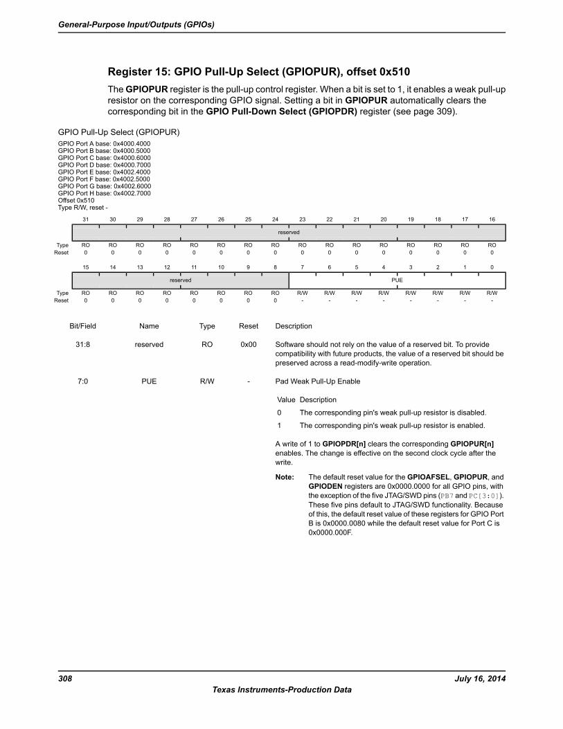
Register 15: GPIO Pull-Up Select (GPIOPUR), offset 0x510TheGPIOPUR register is the pull-up control register. When a bit is set to 1, it enables a weak pull-upresistor on the corresponding GPIO signal. Setting a bit in GPIOPUR automatically clears thecorresponding bit in the GPIO Pull-Down Select (GPIOPDR) register (see page 309).
GPIO Pull-Up Select (GPIOPUR)GPIO Port A base: 0x4000.4000GPIO Port B base: 0x4000.5000GPIO Port C base: 0x4000.6000GPIO Port D base: 0x4000.7000GPIO Port E base: 0x4002.4000GPIO Port F base: 0x4002.5000GPIO Port G base: 0x4002.6000GPIO Port H base: 0x4002.7000Offset 0x510Type R/W, reset -
16171819202122232425262728293031
reserved
ROROROROROROROROROROROROROROROROType0000000000000000Reset
0123456789101112131415
PUEreserved
R/WR/WR/WR/WR/WR/WR/WR/WROROROROROROROROType--------00000000Reset
DescriptionResetTypeNameBit/Field
Software should not rely on the value of a reserved bit. To providecompatibility with future products, the value of a reserved bit should bepreserved across a read-modify-write operation.
0x00ROreserved31:8
Pad Weak Pull-Up Enable
DescriptionValue
The corresponding pin's weak pull-up resistor is disabled.0
The corresponding pin's weak pull-up resistor is enabled.1
A write of 1 to GPIOPDR[n] clears the corresponding GPIOPUR[n]enables. The change is effective on the second clock cycle after thewrite.
Note: The default reset value for the GPIOAFSEL, GPIOPUR, andGPIODEN registers are 0x0000.0000 for all GPIO pins, withthe exception of the five JTAG/SWD pins (PB7 and PC[3:0]).These five pins default to JTAG/SWD functionality. Becauseof this, the default reset value of these registers for GPIO PortB is 0x0000.0080 while the default reset value for Port C is0x0000.000F.
-R/WPUE7:0
July 16, 2014308Texas Instruments-Production Data
General-Purpose Input/Outputs (GPIOs)
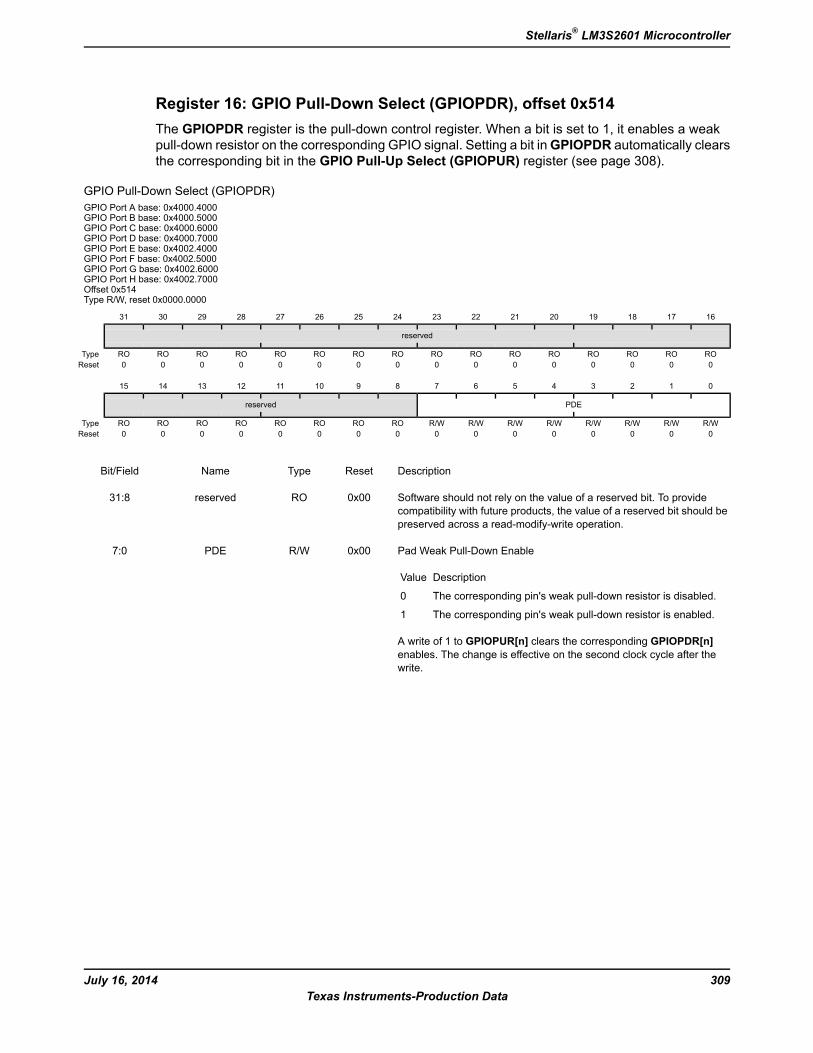
Register 16: GPIO Pull-Down Select (GPIOPDR), offset 0x514The GPIOPDR register is the pull-down control register. When a bit is set to 1, it enables a weakpull-down resistor on the corresponding GPIO signal. Setting a bit inGPIOPDR automatically clearsthe corresponding bit in the GPIO Pull-Up Select (GPIOPUR) register (see page 308).
GPIO Pull-Down Select (GPIOPDR)GPIO Port A base: 0x4000.4000GPIO Port B base: 0x4000.5000GPIO Port C base: 0x4000.6000GPIO Port D base: 0x4000.7000GPIO Port E base: 0x4002.4000GPIO Port F base: 0x4002.5000GPIO Port G base: 0x4002.6000GPIO Port H base: 0x4002.7000Offset 0x514Type R/W, reset 0x0000.0000
16171819202122232425262728293031
reserved
ROROROROROROROROROROROROROROROROType0000000000000000Reset
0123456789101112131415
PDEreserved
R/WR/WR/WR/WR/WR/WR/WR/WROROROROROROROROType0000000000000000Reset
DescriptionResetTypeNameBit/Field
Software should not rely on the value of a reserved bit. To providecompatibility with future products, the value of a reserved bit should bepreserved across a read-modify-write operation.
0x00ROreserved31:8
Pad Weak Pull-Down Enable
DescriptionValue
The corresponding pin's weak pull-down resistor is disabled.0
The corresponding pin's weak pull-down resistor is enabled.1
A write of 1 to GPIOPUR[n] clears the corresponding GPIOPDR[n]enables. The change is effective on the second clock cycle after thewrite.
0x00R/WPDE7:0
309July 16, 2014Texas Instruments-Production Data
Stellaris® LM3S2601 Microcontroller
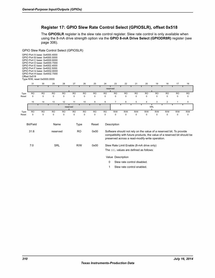
Register 17: GPIO Slew Rate Control Select (GPIOSLR), offset 0x518The GPIOSLR register is the slew rate control register. Slew rate control is only available whenusing the 8-mA drive strength option via the GPIO 8-mA Drive Select (GPIODR8R) register (seepage 306).
GPIO Slew Rate Control Select (GPIOSLR)GPIO Port A base: 0x4000.4000GPIO Port B base: 0x4000.5000GPIO Port C base: 0x4000.6000GPIO Port D base: 0x4000.7000GPIO Port E base: 0x4002.4000GPIO Port F base: 0x4002.5000GPIO Port G base: 0x4002.6000GPIO Port H base: 0x4002.7000Offset 0x518Type R/W, reset 0x0000.0000
16171819202122232425262728293031
reserved
ROROROROROROROROROROROROROROROROType0000000000000000Reset
0123456789101112131415
SRLreserved
R/WR/WR/WR/WR/WR/WR/WR/WROROROROROROROROType0000000000000000Reset
DescriptionResetTypeNameBit/Field
Software should not rely on the value of a reserved bit. To providecompatibility with future products, the value of a reserved bit should bepreserved across a read-modify-write operation.
0x00ROreserved31:8
Slew Rate Limit Enable (8-mA drive only)The SRL values are defined as follows:
DescriptionValue
Slew rate control disabled.0
Slew rate control enabled.1
0x00R/WSRL7:0
July 16, 2014310Texas Instruments-Production Data
General-Purpose Input/Outputs (GPIOs)
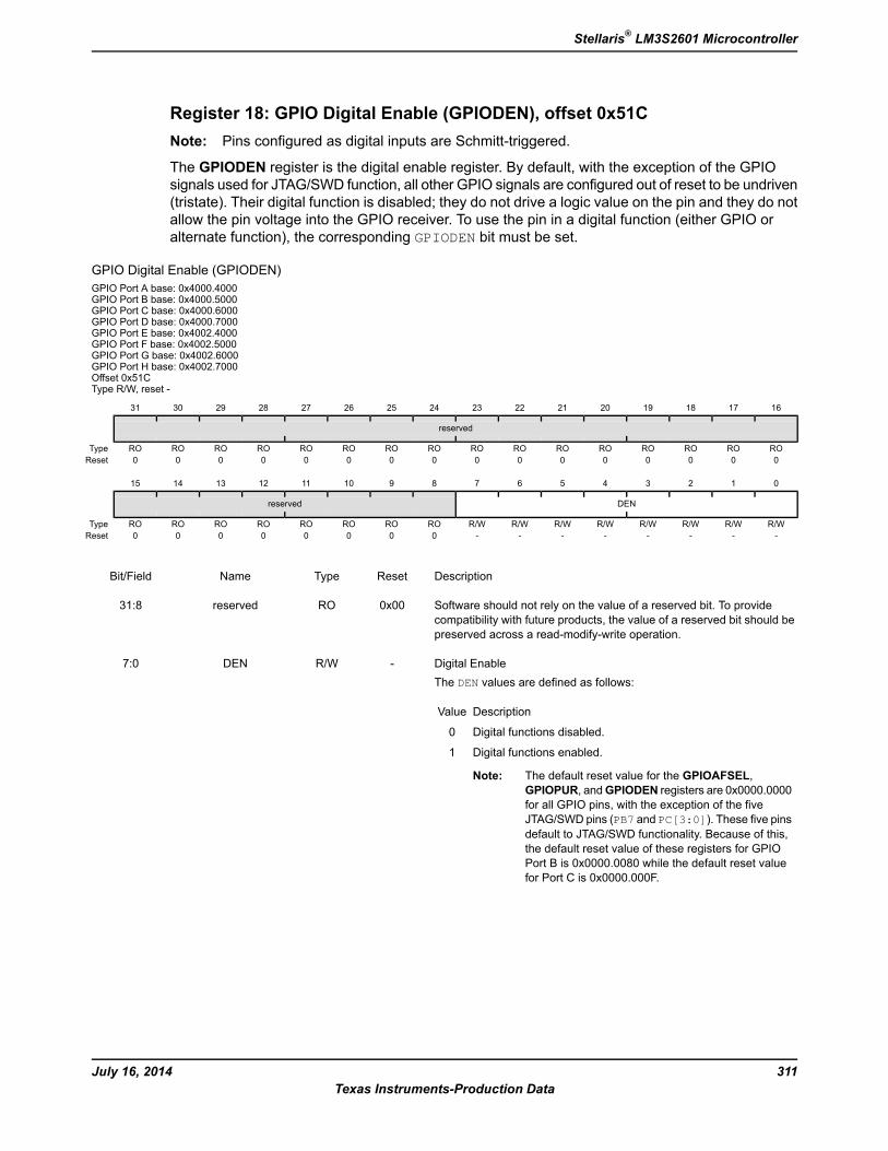
Register 18: GPIO Digital Enable (GPIODEN), offset 0x51CNote: Pins configured as digital inputs are Schmitt-triggered.
The GPIODEN register is the digital enable register. By default, with the exception of the GPIOsignals used for JTAG/SWD function, all other GPIO signals are configured out of reset to be undriven(tristate). Their digital function is disabled; they do not drive a logic value on the pin and they do notallow the pin voltage into the GPIO receiver. To use the pin in a digital function (either GPIO oralternate function), the corresponding GPIODEN bit must be set.
GPIO Digital Enable (GPIODEN)GPIO Port A base: 0x4000.4000GPIO Port B base: 0x4000.5000GPIO Port C base: 0x4000.6000GPIO Port D base: 0x4000.7000GPIO Port E base: 0x4002.4000GPIO Port F base: 0x4002.5000GPIO Port G base: 0x4002.6000GPIO Port H base: 0x4002.7000Offset 0x51CType R/W, reset -
16171819202122232425262728293031
reserved
ROROROROROROROROROROROROROROROROType0000000000000000Reset
0123456789101112131415
DENreserved
R/WR/WR/WR/WR/WR/WR/WR/WROROROROROROROROType--------00000000Reset
DescriptionResetTypeNameBit/Field
Software should not rely on the value of a reserved bit. To providecompatibility with future products, the value of a reserved bit should bepreserved across a read-modify-write operation.
0x00ROreserved31:8
Digital EnableThe DEN values are defined as follows:
DescriptionValue
Digital functions disabled.0
Digital functions enabled.1
Note: The default reset value for the GPIOAFSEL,GPIOPUR, andGPIODEN registers are 0x0000.0000for all GPIO pins, with the exception of the fiveJTAG/SWD pins (PB7 and PC[3:0]). These five pinsdefault to JTAG/SWD functionality. Because of this,the default reset value of these registers for GPIOPort B is 0x0000.0080 while the default reset valuefor Port C is 0x0000.000F.
-R/WDEN7:0
311July 16, 2014Texas Instruments-Production Data
Stellaris® LM3S2601 Microcontroller
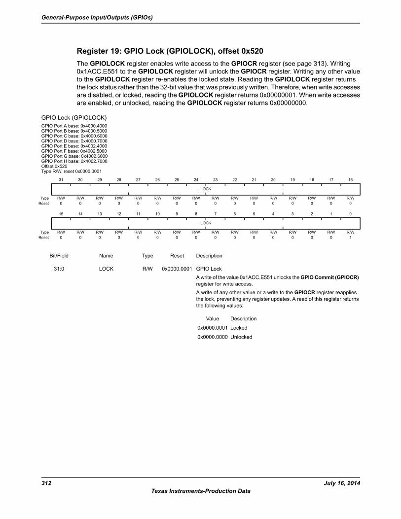
Register 19: GPIO Lock (GPIOLOCK), offset 0x520The GPIOLOCK register enables write access to the GPIOCR register (see page 313). Writing0x1ACC.E551 to the GPIOLOCK register will unlock the GPIOCR register. Writing any other valueto the GPIOLOCK register re-enables the locked state. Reading the GPIOLOCK register returnsthe lock status rather than the 32-bit value that was previously written. Therefore, when write accessesare disabled, or locked, reading theGPIOLOCK register returns 0x00000001. When write accessesare enabled, or unlocked, reading the GPIOLOCK register returns 0x00000000.
GPIO Lock (GPIOLOCK)GPIO Port A base: 0x4000.4000GPIO Port B base: 0x4000.5000GPIO Port C base: 0x4000.6000GPIO Port D base: 0x4000.7000GPIO Port E base: 0x4002.4000GPIO Port F base: 0x4002.5000GPIO Port G base: 0x4002.6000GPIO Port H base: 0x4002.7000Offset 0x520Type R/W, reset 0x0000.0001
16171819202122232425262728293031
LOCK
R/WR/WR/WR/WR/WR/WR/WR/WR/WR/WR/WR/WR/WR/WR/WR/WType0000000000000000Reset
0123456789101112131415
LOCK
R/WR/WR/WR/WR/WR/WR/WR/WR/WR/WR/WR/WR/WR/WR/WR/WType1000000000000000Reset
DescriptionResetTypeNameBit/Field
GPIO LockA write of the value 0x1ACC.E551 unlocks theGPIOCommit (GPIOCR)register for write access.A write of any other value or a write to the GPIOCR register reappliesthe lock, preventing any register updates. A read of this register returnsthe following values:
DescriptionValue
Locked0x0000.0001
Unlocked0x0000.0000
0x0000.0001R/WLOCK31:0
July 16, 2014312Texas Instruments-Production Data
General-Purpose Input/Outputs (GPIOs)
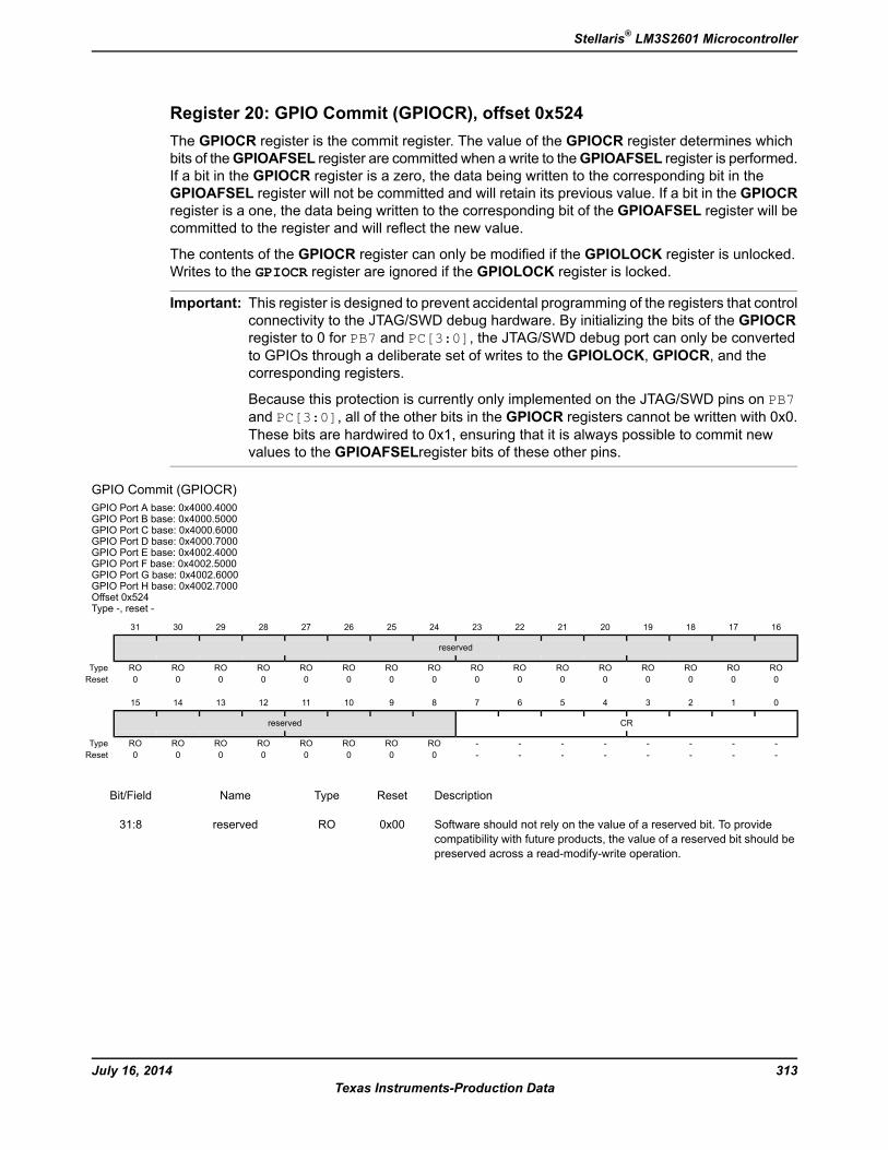
Register 20: GPIO Commit (GPIOCR), offset 0x524The GPIOCR register is the commit register. The value of the GPIOCR register determines whichbits of theGPIOAFSEL register are committed when a write to theGPIOAFSEL register is performed.If a bit in the GPIOCR register is a zero, the data being written to the corresponding bit in theGPIOAFSEL register will not be committed and will retain its previous value. If a bit in the GPIOCRregister is a one, the data being written to the corresponding bit of the GPIOAFSEL register will becommitted to the register and will reflect the new value.
The contents of the GPIOCR register can only be modified if the GPIOLOCK register is unlocked.Writes to the GPIOCR register are ignored if the GPIOLOCK register is locked.
Important: This register is designed to prevent accidental programming of the registers that controlconnectivity to the JTAG/SWD debug hardware. By initializing the bits of the GPIOCRregister to 0 for PB7 and PC[3:0], the JTAG/SWD debug port can only be convertedto GPIOs through a deliberate set of writes to the GPIOLOCK, GPIOCR, and thecorresponding registers.
Because this protection is currently only implemented on the JTAG/SWD pins on PB7and PC[3:0], all of the other bits in the GPIOCR registers cannot be written with 0x0.These bits are hardwired to 0x1, ensuring that it is always possible to commit newvalues to the GPIOAFSELregister bits of these other pins.
GPIO Commit (GPIOCR)GPIO Port A base: 0x4000.4000GPIO Port B base: 0x4000.5000GPIO Port C base: 0x4000.6000GPIO Port D base: 0x4000.7000GPIO Port E base: 0x4002.4000GPIO Port F base: 0x4002.5000GPIO Port G base: 0x4002.6000GPIO Port H base: 0x4002.7000Offset 0x524Type -, reset -
16171819202122232425262728293031
reserved
ROROROROROROROROROROROROROROROROType0000000000000000Reset
0123456789101112131415
CRreserved
--------ROROROROROROROROType--------00000000Reset
DescriptionResetTypeNameBit/Field
Software should not rely on the value of a reserved bit. To providecompatibility with future products, the value of a reserved bit should bepreserved across a read-modify-write operation.
0x00ROreserved31:8
313July 16, 2014Texas Instruments-Production Data
Stellaris® LM3S2601 Microcontroller
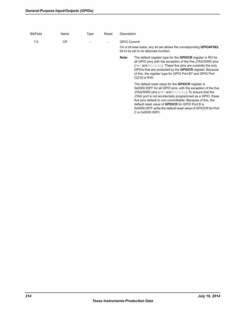
DescriptionResetTypeNameBit/Field
GPIO CommitOn a bit-wise basis, any bit set allows the corresponding GPIOAFSELbit to be set to its alternate function.
Note: The default register type for the GPIOCR register is RO forall GPIO pins with the exception of the five JTAG/SWD pins(PB7 and PC[3:0]). These five pins are currently the onlyGPIOs that are protected by the GPIOCR register. Becauseof this, the register type for GPIO Port B7 and GPIO PortC[3:0] is R/W.
The default reset value for the GPIOCR register is0x0000.00FF for all GPIO pins, with the exception of the fiveJTAG/SWD pins (PB7 and PC[3:0]). To ensure that theJTAG port is not accidentally programmed as a GPIO, thesefive pins default to non-committable. Because of this, thedefault reset value of GPIOCR for GPIO Port B is0x0000.007F while the default reset value of GPIOCR for PortC is 0x0000.00F0.
--CR7:0
July 16, 2014314Texas Instruments-Production Data
General-Purpose Input/Outputs (GPIOs)
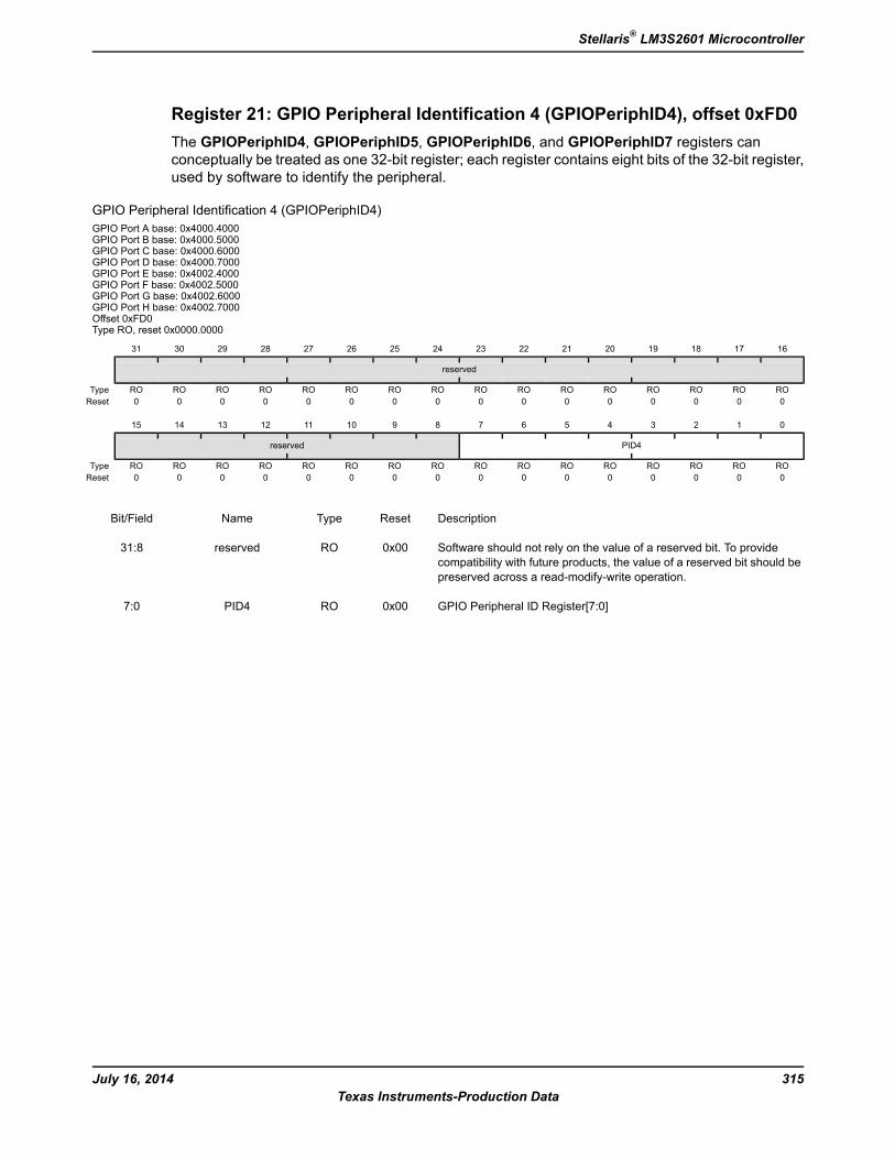
Register 21: GPIO Peripheral Identification 4 (GPIOPeriphID4), offset 0xFD0The GPIOPeriphID4, GPIOPeriphID5, GPIOPeriphID6, and GPIOPeriphID7 registers canconceptually be treated as one 32-bit register; each register contains eight bits of the 32-bit register,used by software to identify the peripheral.
GPIO Peripheral Identification 4 (GPIOPeriphID4)GPIO Port A base: 0x4000.4000GPIO Port B base: 0x4000.5000GPIO Port C base: 0x4000.6000GPIO Port D base: 0x4000.7000GPIO Port E base: 0x4002.4000GPIO Port F base: 0x4002.5000GPIO Port G base: 0x4002.6000GPIO Port H base: 0x4002.7000Offset 0xFD0Type RO, reset 0x0000.0000
16171819202122232425262728293031
reserved
ROROROROROROROROROROROROROROROROType0000000000000000Reset
0123456789101112131415
PID4reserved
ROROROROROROROROROROROROROROROROType0000000000000000Reset
DescriptionResetTypeNameBit/Field
Software should not rely on the value of a reserved bit. To providecompatibility with future products, the value of a reserved bit should bepreserved across a read-modify-write operation.
0x00ROreserved31:8
GPIO Peripheral ID Register[7:0]0x00ROPID47:0
315July 16, 2014Texas Instruments-Production Data
Stellaris® LM3S2601 Microcontroller
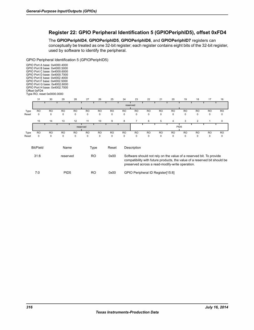
Register 22: GPIO Peripheral Identification 5 (GPIOPeriphID5), offset 0xFD4The GPIOPeriphID4, GPIOPeriphID5, GPIOPeriphID6, and GPIOPeriphID7 registers canconceptually be treated as one 32-bit register; each register contains eight bits of the 32-bit register,used by software to identify the peripheral.
GPIO Peripheral Identification 5 (GPIOPeriphID5)GPIO Port A base: 0x4000.4000GPIO Port B base: 0x4000.5000GPIO Port C base: 0x4000.6000GPIO Port D base: 0x4000.7000GPIO Port E base: 0x4002.4000GPIO Port F base: 0x4002.5000GPIO Port G base: 0x4002.6000GPIO Port H base: 0x4002.7000Offset 0xFD4Type RO, reset 0x0000.0000
16171819202122232425262728293031
reserved
ROROROROROROROROROROROROROROROROType0000000000000000Reset
0123456789101112131415
PID5reserved
ROROROROROROROROROROROROROROROROType0000000000000000Reset
DescriptionResetTypeNameBit/Field
Software should not rely on the value of a reserved bit. To providecompatibility with future products, the value of a reserved bit should bepreserved across a read-modify-write operation.
0x00ROreserved31:8
GPIO Peripheral ID Register[15:8]0x00ROPID57:0
July 16, 2014316Texas Instruments-Production Data
General-Purpose Input/Outputs (GPIOs)

Register 23: GPIO Peripheral Identification 6 (GPIOPeriphID6), offset 0xFD8The GPIOPeriphID4, GPIOPeriphID5, GPIOPeriphID6, and GPIOPeriphID7 registers canconceptually be treated as one 32-bit register; each register contains eight bits of the 32-bit register,used by software to identify the peripheral.
GPIO Peripheral Identification 6 (GPIOPeriphID6)GPIO Port A base: 0x4000.4000GPIO Port B base: 0x4000.5000GPIO Port C base: 0x4000.6000GPIO Port D base: 0x4000.7000GPIO Port E base: 0x4002.4000GPIO Port F base: 0x4002.5000GPIO Port G base: 0x4002.6000GPIO Port H base: 0x4002.7000Offset 0xFD8Type RO, reset 0x0000.0000
16171819202122232425262728293031
reserved
ROROROROROROROROROROROROROROROROType0000000000000000Reset
0123456789101112131415
PID6reserved
ROROROROROROROROROROROROROROROROType0000000000000000Reset
DescriptionResetTypeNameBit/Field
Software should not rely on the value of a reserved bit. To providecompatibility with future products, the value of a reserved bit should bepreserved across a read-modify-write operation.
0x00ROreserved31:8
GPIO Peripheral ID Register[23:16]0x00ROPID67:0
317July 16, 2014Texas Instruments-Production Data
Stellaris® LM3S2601 Microcontroller

Register 24: GPIO Peripheral Identification 7 (GPIOPeriphID7), offset 0xFDCThe GPIOPeriphID4, GPIOPeriphID5, GPIOPeriphID6, and GPIOPeriphID7 registers canconceptually be treated as one 32-bit register; each register contains eight bits of the 32-bit register,used by software to identify the peripheral.
GPIO Peripheral Identification 7 (GPIOPeriphID7)GPIO Port A base: 0x4000.4000GPIO Port B base: 0x4000.5000GPIO Port C base: 0x4000.6000GPIO Port D base: 0x4000.7000GPIO Port E base: 0x4002.4000GPIO Port F base: 0x4002.5000GPIO Port G base: 0x4002.6000GPIO Port H base: 0x4002.7000Offset 0xFDCType RO, reset 0x0000.0000
16171819202122232425262728293031
reserved
ROROROROROROROROROROROROROROROROType0000000000000000Reset
0123456789101112131415
PID7reserved
ROROROROROROROROROROROROROROROROType0000000000000000Reset
DescriptionResetTypeNameBit/Field
Software should not rely on the value of a reserved bit. To providecompatibility with future products, the value of a reserved bit should bepreserved across a read-modify-write operation.
0x00ROreserved31:8
GPIO Peripheral ID Register[31:24]0x00ROPID77:0
July 16, 2014318Texas Instruments-Production Data
General-Purpose Input/Outputs (GPIOs)
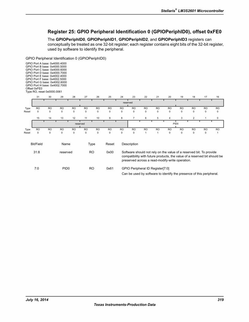
Register 25: GPIO Peripheral Identification 0 (GPIOPeriphID0), offset 0xFE0The GPIOPeriphID0, GPIOPeriphID1, GPIOPeriphID2, and GPIOPeriphID3 registers canconceptually be treated as one 32-bit register; each register contains eight bits of the 32-bit register,used by software to identify the peripheral.
GPIO Peripheral Identification 0 (GPIOPeriphID0)GPIO Port A base: 0x4000.4000GPIO Port B base: 0x4000.5000GPIO Port C base: 0x4000.6000GPIO Port D base: 0x4000.7000GPIO Port E base: 0x4002.4000GPIO Port F base: 0x4002.5000GPIO Port G base: 0x4002.6000GPIO Port H base: 0x4002.7000Offset 0xFE0Type RO, reset 0x0000.0061
16171819202122232425262728293031
reserved
ROROROROROROROROROROROROROROROROType0000000000000000Reset
0123456789101112131415
PID0reserved
ROROROROROROROROROROROROROROROROType1000011000000000Reset
DescriptionResetTypeNameBit/Field
Software should not rely on the value of a reserved bit. To providecompatibility with future products, the value of a reserved bit should bepreserved across a read-modify-write operation.
0x00ROreserved31:8
GPIO Peripheral ID Register[7:0]Can be used by software to identify the presence of this peripheral.
0x61ROPID07:0
319July 16, 2014Texas Instruments-Production Data
Stellaris® LM3S2601 Microcontroller

Register 26: GPIO Peripheral Identification 1 (GPIOPeriphID1), offset 0xFE4The GPIOPeriphID0, GPIOPeriphID1, GPIOPeriphID2, and GPIOPeriphID3 registers canconceptually be treated as one 32-bit register; each register contains eight bits of the 32-bit register,used by software to identify the peripheral.
GPIO Peripheral Identification 1 (GPIOPeriphID1)GPIO Port A base: 0x4000.4000GPIO Port B base: 0x4000.5000GPIO Port C base: 0x4000.6000GPIO Port D base: 0x4000.7000GPIO Port E base: 0x4002.4000GPIO Port F base: 0x4002.5000GPIO Port G base: 0x4002.6000GPIO Port H base: 0x4002.7000Offset 0xFE4Type RO, reset 0x0000.0000
16171819202122232425262728293031
reserved
ROROROROROROROROROROROROROROROROType0000000000000000Reset
0123456789101112131415
PID1reserved
ROROROROROROROROROROROROROROROROType0000000000000000Reset
DescriptionResetTypeNameBit/Field
Software should not rely on the value of a reserved bit. To providecompatibility with future products, the value of a reserved bit should bepreserved across a read-modify-write operation.
0x00ROreserved31:8
GPIO Peripheral ID Register[15:8]Can be used by software to identify the presence of this peripheral.
0x00ROPID17:0
July 16, 2014320Texas Instruments-Production Data
General-Purpose Input/Outputs (GPIOs)

Register 27: GPIO Peripheral Identification 2 (GPIOPeriphID2), offset 0xFE8The GPIOPeriphID0, GPIOPeriphID1, GPIOPeriphID2, and GPIOPeriphID3 registers canconceptually be treated as one 32-bit register; each register contains eight bits of the 32-bit register,used by software to identify the peripheral.
GPIO Peripheral Identification 2 (GPIOPeriphID2)GPIO Port A base: 0x4000.4000GPIO Port B base: 0x4000.5000GPIO Port C base: 0x4000.6000GPIO Port D base: 0x4000.7000GPIO Port E base: 0x4002.4000GPIO Port F base: 0x4002.5000GPIO Port G base: 0x4002.6000GPIO Port H base: 0x4002.7000Offset 0xFE8Type RO, reset 0x0000.0018
16171819202122232425262728293031
reserved
ROROROROROROROROROROROROROROROROType0000000000000000Reset
0123456789101112131415
PID2reserved
ROROROROROROROROROROROROROROROROType0001100000000000Reset
DescriptionResetTypeNameBit/Field
Software should not rely on the value of a reserved bit. To providecompatibility with future products, the value of a reserved bit should bepreserved across a read-modify-write operation.
0x00ROreserved31:8
GPIO Peripheral ID Register[23:16]Can be used by software to identify the presence of this peripheral.
0x18ROPID27:0
321July 16, 2014Texas Instruments-Production Data
Stellaris® LM3S2601 Microcontroller
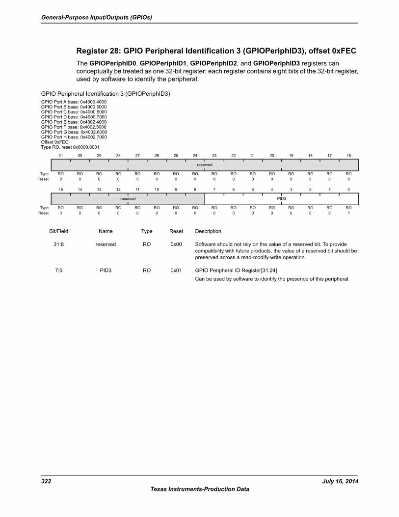
Register 28: GPIO Peripheral Identification 3 (GPIOPeriphID3), offset 0xFECThe GPIOPeriphID0, GPIOPeriphID1, GPIOPeriphID2, and GPIOPeriphID3 registers canconceptually be treated as one 32-bit register; each register contains eight bits of the 32-bit register,used by software to identify the peripheral.
GPIO Peripheral Identification 3 (GPIOPeriphID3)GPIO Port A base: 0x4000.4000GPIO Port B base: 0x4000.5000GPIO Port C base: 0x4000.6000GPIO Port D base: 0x4000.7000GPIO Port E base: 0x4002.4000GPIO Port F base: 0x4002.5000GPIO Port G base: 0x4002.6000GPIO Port H base: 0x4002.7000Offset 0xFECType RO, reset 0x0000.0001
16171819202122232425262728293031
reserved
ROROROROROROROROROROROROROROROROType0000000000000000Reset
0123456789101112131415
PID3reserved
ROROROROROROROROROROROROROROROROType1000000000000000Reset
DescriptionResetTypeNameBit/Field
Software should not rely on the value of a reserved bit. To providecompatibility with future products, the value of a reserved bit should bepreserved across a read-modify-write operation.
0x00ROreserved31:8
GPIO Peripheral ID Register[31:24]Can be used by software to identify the presence of this peripheral.
0x01ROPID37:0
July 16, 2014322Texas Instruments-Production Data
General-Purpose Input/Outputs (GPIOs)
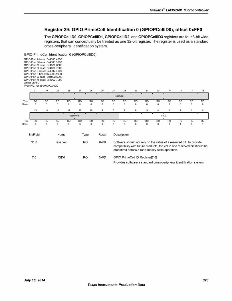
Register 29: GPIO PrimeCell Identification 0 (GPIOPCellID0), offset 0xFF0TheGPIOPCellID0,GPIOPCellID1,GPIOPCellID2, andGPIOPCellID3 registers are four 8-bit wideregisters, that can conceptually be treated as one 32-bit register. The register is used as a standardcross-peripheral identification system.
GPIO PrimeCell Identification 0 (GPIOPCellID0)GPIO Port A base: 0x4000.4000GPIO Port B base: 0x4000.5000GPIO Port C base: 0x4000.6000GPIO Port D base: 0x4000.7000GPIO Port E base: 0x4002.4000GPIO Port F base: 0x4002.5000GPIO Port G base: 0x4002.6000GPIO Port H base: 0x4002.7000Offset 0xFF0Type RO, reset 0x0000.000D
16171819202122232425262728293031
reserved
ROROROROROROROROROROROROROROROROType0000000000000000Reset
0123456789101112131415
CID0reserved
ROROROROROROROROROROROROROROROROType1011000000000000Reset
DescriptionResetTypeNameBit/Field
Software should not rely on the value of a reserved bit. To providecompatibility with future products, the value of a reserved bit should bepreserved across a read-modify-write operation.
0x00ROreserved31:8
GPIO PrimeCell ID Register[7:0]Provides software a standard cross-peripheral identification system.
0x0DROCID07:0
323July 16, 2014Texas Instruments-Production Data
Stellaris® LM3S2601 Microcontroller
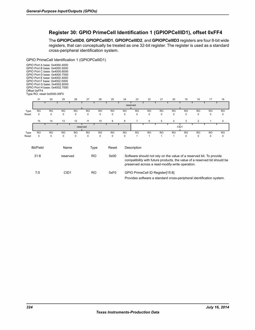
Register 30: GPIO PrimeCell Identification 1 (GPIOPCellID1), offset 0xFF4TheGPIOPCellID0,GPIOPCellID1,GPIOPCellID2, andGPIOPCellID3 registers are four 8-bit wideregisters, that can conceptually be treated as one 32-bit register. The register is used as a standardcross-peripheral identification system.
GPIO PrimeCell Identification 1 (GPIOPCellID1)GPIO Port A base: 0x4000.4000GPIO Port B base: 0x4000.5000GPIO Port C base: 0x4000.6000GPIO Port D base: 0x4000.7000GPIO Port E base: 0x4002.4000GPIO Port F base: 0x4002.5000GPIO Port G base: 0x4002.6000GPIO Port H base: 0x4002.7000Offset 0xFF4Type RO, reset 0x0000.00F0
16171819202122232425262728293031
reserved
ROROROROROROROROROROROROROROROROType0000000000000000Reset
0123456789101112131415
CID1reserved
ROROROROROROROROROROROROROROROROType0000111100000000Reset
DescriptionResetTypeNameBit/Field
Software should not rely on the value of a reserved bit. To providecompatibility with future products, the value of a reserved bit should bepreserved across a read-modify-write operation.
0x00ROreserved31:8
GPIO PrimeCell ID Register[15:8]Provides software a standard cross-peripheral identification system.
0xF0ROCID17:0
July 16, 2014324Texas Instruments-Production Data
General-Purpose Input/Outputs (GPIOs)

Register 31: GPIO PrimeCell Identification 2 (GPIOPCellID2), offset 0xFF8TheGPIOPCellID0,GPIOPCellID1,GPIOPCellID2, andGPIOPCellID3 registers are four 8-bit wideregisters, that can conceptually be treated as one 32-bit register. The register is used as a standardcross-peripheral identification system.
GPIO PrimeCell Identification 2 (GPIOPCellID2)GPIO Port A base: 0x4000.4000GPIO Port B base: 0x4000.5000GPIO Port C base: 0x4000.6000GPIO Port D base: 0x4000.7000GPIO Port E base: 0x4002.4000GPIO Port F base: 0x4002.5000GPIO Port G base: 0x4002.6000GPIO Port H base: 0x4002.7000Offset 0xFF8Type RO, reset 0x0000.0005
16171819202122232425262728293031
reserved
ROROROROROROROROROROROROROROROROType0000000000000000Reset
0123456789101112131415
CID2reserved
ROROROROROROROROROROROROROROROROType1010000000000000Reset
DescriptionResetTypeNameBit/Field
Software should not rely on the value of a reserved bit. To providecompatibility with future products, the value of a reserved bit should bepreserved across a read-modify-write operation.
0x00ROreserved31:8
GPIO PrimeCell ID Register[23:16]Provides software a standard cross-peripheral identification system.
0x05ROCID27:0
325July 16, 2014Texas Instruments-Production Data
Stellaris® LM3S2601 Microcontroller

Register 32: GPIO PrimeCell Identification 3 (GPIOPCellID3), offset 0xFFCTheGPIOPCellID0,GPIOPCellID1,GPIOPCellID2, andGPIOPCellID3 registers are four 8-bit wideregisters, that can conceptually be treated as one 32-bit register. The register is used as a standardcross-peripheral identification system.
GPIO PrimeCell Identification 3 (GPIOPCellID3)GPIO Port A base: 0x4000.4000GPIO Port B base: 0x4000.5000GPIO Port C base: 0x4000.6000GPIO Port D base: 0x4000.7000GPIO Port E base: 0x4002.4000GPIO Port F base: 0x4002.5000GPIO Port G base: 0x4002.6000GPIO Port H base: 0x4002.7000Offset 0xFFCType RO, reset 0x0000.00B1
16171819202122232425262728293031
reserved
ROROROROROROROROROROROROROROROROType0000000000000000Reset
0123456789101112131415
CID3reserved
ROROROROROROROROROROROROROROROROType1000110100000000Reset
DescriptionResetTypeNameBit/Field
Software should not rely on the value of a reserved bit. To providecompatibility with future products, the value of a reserved bit should bepreserved across a read-modify-write operation.
0x00ROreserved31:8
GPIO PrimeCell ID Register[31:24]Provides software a standard cross-peripheral identification system.
0xB1ROCID37:0
July 16, 2014326Texas Instruments-Production Data
General-Purpose Input/Outputs (GPIOs)
9 General-Purpose TimersProgrammable timers can be used to count or time external events that drive the Timer input pins.The Stellaris® General-Purpose Timer Module (GPTM) contains four GPTM blocks (Timer0, Timer1,Timer 2, and Timer 3). Each GPTM block provides two 16-bit timers/counters (referred to as TimerAand TimerB) that can be configured to operate independently as timers or event counters, orconfigured to operate as one 32-bit timer or one 32-bit Real-Time Clock (RTC).
The GPT Module is one timing resource available on the Stellaris microcontrollers. Other timerresources include the System Timer (SysTick) (see 88).
The General-Purpose Timers provide the following features:
Four General-Purpose Timer Modules (GPTM), each of which provides two 16-bit timers/counters.Each GPTM can be configured to operate independently:
– As a single 32-bit timer
– As one 32-bit Real-Time Clock (RTC) to event capture
– For Pulse Width Modulation (PWM)
32-bit Timer modes
– Programmable one-shot timer
– Programmable periodic timer
– Real-Time Clock when using an external 32.768-KHz clock as the input
– User-enabled stalling when the controller asserts CPU Halt flag during debug
16-bit Timer modes
– General-purpose timer function with an 8-bit prescaler (for one-shot and periodic modes only)
– Programmable one-shot timer
– Programmable periodic timer
– User-enabled stalling when the controller asserts CPU Halt flag during debug
16-bit Input Capture modes
– Input edge count capture
– Input edge time capture
16-bit PWM mode
– Simple PWM mode with software-programmable output inversion of the PWM signal
9.1 Block DiagramNote: In Figure 9-1 on page 328, the specific CCP pins available depend on the Stellaris device.
See Table 9-1 on page 328 for the available CCPs.
327July 16, 2014Texas Instruments-Production Data
Stellaris® LM3S2601 Microcontroller
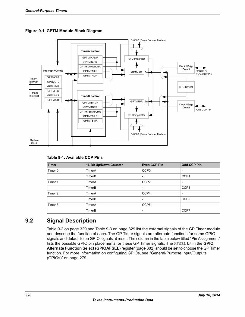
Figure 9-1. GPTM Module Block Diagram
TA Comparator
TB Comparator
GPTMTBR
GPTMAR
Clock / EdgeDetect
RTC Divider
Clock / EdgeDetect
TimerAInterrupt
TimerBInterrupt
SystemClock
0x0000 (Down Counter Modes)
0x0000 (Down Counter Modes)
32 KHz orEven CCP Pin
Odd CCP Pin
En
En
TimerA Control
GPTMTAPMR
GPTMTAILR
GPTMTAMATCHR
GPTMTAPR
GPTMTAMR
TimerB Control
GPTMTBPMR
GPTMTBILR
GPTMTBMATCHR
GPTMTBPR
GPTMTBMR
Interrupt / Config
GPTMCFG
GPTMRIS
GPTMICR
GPTMMIS
GPTMIMR
GPTMCTL
Table 9-1. Available CCP Pins
Odd CCP PinEven CCP Pin16-Bit Up/Down CounterTimer
-CCP0TimerATimer 0
CCP1-TimerB
-CCP2TimerATimer 1
CCP3-TimerB
-CCP4TimerATimer 2
CCP5-TimerB
-CCP6TimerATimer 3
CCP7-TimerB
9.2 Signal DescriptionTable 9-2 on page 329 and Table 9-3 on page 329 list the external signals of the GP Timer moduleand describe the function of each. The GP Timer signals are alternate functions for some GPIOsignals and default to be GPIO signals at reset. The column in the table below titled "Pin Assignment"lists the possible GPIO pin placements for these GP Timer signals. The AFSEL bit in the GPIOAlternate Function Select (GPIOAFSEL) register (page 302) should be set to choose the GP Timerfunction. For more information on configuring GPIOs, see “General-Purpose Input/Outputs(GPIOs)” on page 279.
July 16, 2014328Texas Instruments-Production Data
General-Purpose Timers
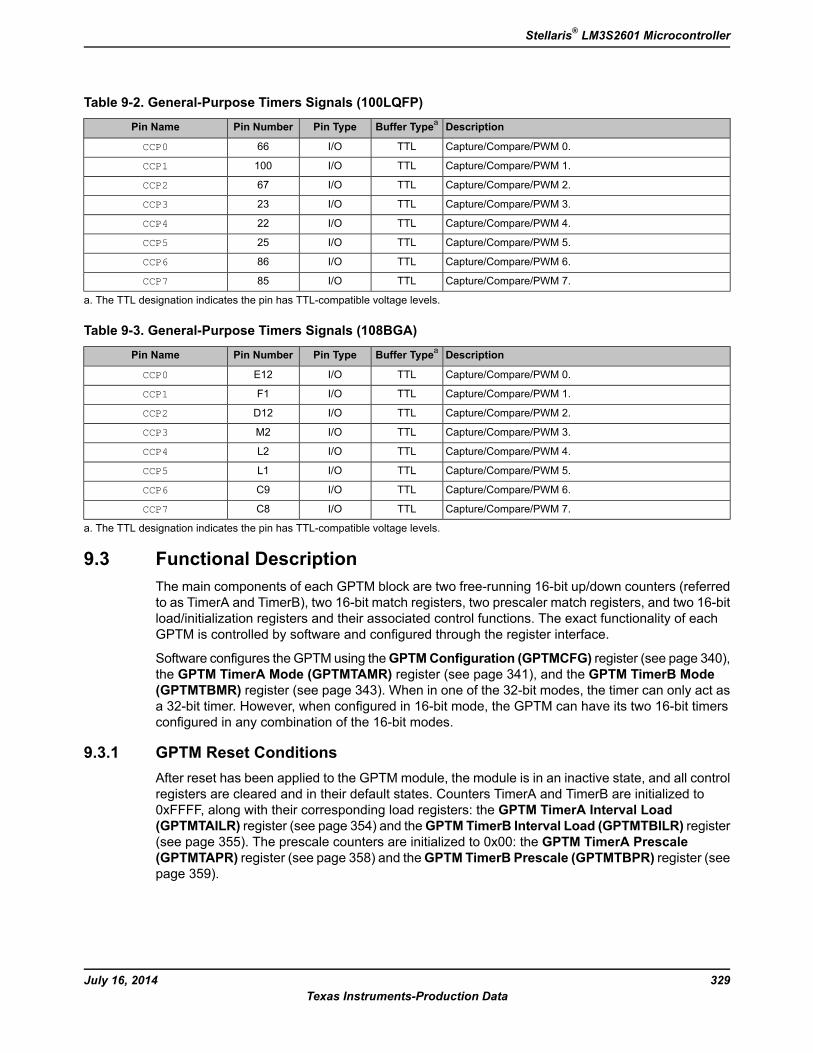
Table 9-2. General-Purpose Timers Signals (100LQFP)
DescriptionBuffer TypeaPin TypePin NumberPin Name
Capture/Compare/PWM 0.TTLI/O66CCP0
Capture/Compare/PWM 1.TTLI/O100CCP1
Capture/Compare/PWM 2.TTLI/O67CCP2
Capture/Compare/PWM 3.TTLI/O23CCP3
Capture/Compare/PWM 4.TTLI/O22CCP4
Capture/Compare/PWM 5.TTLI/O25CCP5
Capture/Compare/PWM 6.TTLI/O86CCP6
Capture/Compare/PWM 7.TTLI/O85CCP7
a. The TTL designation indicates the pin has TTL-compatible voltage levels.
Table 9-3. General-Purpose Timers Signals (108BGA)
DescriptionBuffer TypeaPin TypePin NumberPin Name
Capture/Compare/PWM 0.TTLI/OE12CCP0
Capture/Compare/PWM 1.TTLI/OF1CCP1
Capture/Compare/PWM 2.TTLI/OD12CCP2
Capture/Compare/PWM 3.TTLI/OM2CCP3
Capture/Compare/PWM 4.TTLI/OL2CCP4
Capture/Compare/PWM 5.TTLI/OL1CCP5
Capture/Compare/PWM 6.TTLI/OC9CCP6
Capture/Compare/PWM 7.TTLI/OC8CCP7
a. The TTL designation indicates the pin has TTL-compatible voltage levels.
9.3 Functional DescriptionThe main components of each GPTM block are two free-running 16-bit up/down counters (referredto as TimerA and TimerB), two 16-bit match registers, two prescaler match registers, and two 16-bitload/initialization registers and their associated control functions. The exact functionality of eachGPTM is controlled by software and configured through the register interface.
Software configures the GPTM using theGPTMConfiguration (GPTMCFG) register (see page 340),the GPTM TimerA Mode (GPTMTAMR) register (see page 341), and the GPTM TimerB Mode(GPTMTBMR) register (see page 343). When in one of the 32-bit modes, the timer can only act asa 32-bit timer. However, when configured in 16-bit mode, the GPTM can have its two 16-bit timersconfigured in any combination of the 16-bit modes.
9.3.1 GPTM Reset ConditionsAfter reset has been applied to the GPTM module, the module is in an inactive state, and all controlregisters are cleared and in their default states. Counters TimerA and TimerB are initialized to0xFFFF, along with their corresponding load registers: the GPTM TimerA Interval Load(GPTMTAILR) register (see page 354) and theGPTMTimerB Interval Load (GPTMTBILR) register(see page 355). The prescale counters are initialized to 0x00: the GPTM TimerA Prescale(GPTMTAPR) register (see page 358) and theGPTMTimerB Prescale (GPTMTBPR) register (seepage 359).
329July 16, 2014Texas Instruments-Production Data
Stellaris® LM3S2601 Microcontroller
9.3.2 32-Bit Timer Operating ModesThis section describes the three GPTM 32-bit timer modes (One-Shot, Periodic, and RTC) and theirconfiguration.
The GPTM is placed into 32-bit mode by writing a 0 (One-Shot/Periodic 32-bit timer mode) or a 1(RTCmode) to theGPTMConfiguration (GPTMCFG) register. In both configurations, certain GPTMregisters are concatenated to form pseudo 32-bit registers. These registers include:
GPTM TimerA Interval Load (GPTMTAILR) register [15:0], see page 354
GPTM TimerB Interval Load (GPTMTBILR) register [15:0], see page 355
GPTM TimerA (GPTMTAR) register [15:0], see page 362
GPTM TimerB (GPTMTBR) register [15:0], see page 363
In the 32-bit modes, the GPTM translates a 32-bit write access to GPTMTAILR into a write accessto both GPTMTAILR and GPTMTBILR. The resulting word ordering for such a write operation is:
GPTMTBILR[15:0]:GPTMTAILR[15:0]
Likewise, a read access to GPTMTAR returns the value:
GPTMTBR[15:0]:GPTMTAR[15:0]
9.3.2.1 32-Bit One-Shot/Periodic Timer ModeIn 32-bit one-shot and periodic timer modes, the concatenated versions of the TimerA and TimerBregisters are configured as a 32-bit down-counter. The selection of one-shot or periodic mode isdetermined by the value written to the TAMR field of theGPTM TimerAMode (GPTMTAMR) register(see page 341), and there is no need to write to the GPTM TimerB Mode (GPTMTBMR) register.
When software writes the TAEN bit in the GPTM Control (GPTMCTL) register (see page 345), thetimer begins counting down from its preloaded value. Once the 0x0000.0000 state is reached, thetimer reloads its start value from the concatenated GPTMTAILR on the next cycle. If configured tobe a one-shot timer, the timer stops counting and clears the TAEN bit in the GPTMCTL register. Ifconfigured as a periodic timer, it continues counting.
In addition to reloading the count value, the GPTM generates interrupts and triggers when it reachesthe 0x000.0000 state. The GPTM sets the TATORIS bit in the GPTM Raw Interrupt Status(GPTMRIS) register (see page 350), and holds it until it is cleared by writing the GPTM InterruptClear (GPTMICR) register (see page 352). If the time-out interrupt is enabled in theGPTM InterruptMask (GPTMIMR) register (see page 348), theGPTMalso sets the TATOMIS bit in theGPTMMaskedInterrupt Status (GPTMMIS) register (see page 351).
If software reloads theGPTMTAILR register while the counter is running, the counter loads the newvalue on the next clock cycle and continues counting from the new value.
If the TASTALL bit in the GPTMCTL register is set, the timer freezes counting while the processoris halted by the debugger. The timer resumes counting when the processor resumes execution.
9.3.2.2 32-Bit Real-Time Clock Timer ModeIn Real-Time Clock (RTC) mode, the concatenated versions of the TimerA and TimerB registersare configured as a 32-bit up-counter. When RTC mode is selected for the first time, the counter isloaded with a value of 0x0000.0001. All subsequent load values must be written to theGPTMTimerAMatch (GPTMTAMATCHR) register (see page 356) by the controller.
July 16, 2014330Texas Instruments-Production Data
General-Purpose Timers
The input clock on an even CCP input is required to be 32.768 KHz in RTC mode. The clock signalis then divided down to a 1 Hz rate and is passed along to the input of the 32-bit counter.
When software writes the TAEN bit inthe GPTMCTL register, the counter starts counting up from itspreloaded value of 0x0000.0001. When the current count value matches the preloaded value in theGPTMTAMATCHR register, it rolls over to a value of 0x0000.0000 and continues counting untileither a hardware reset, or it is disabled by software (clearing the TAEN bit). When a match occurs,the GPTM asserts the RTCRIS bit in GPTMRIS. If the RTC interrupt is enabled in GPTMIMR, theGPTM also sets the RTCMIS bit in GPTMMIS and generates a controller interrupt. The status flagsare cleared by writing the RTCCINT bit in GPTMICR.
If the TASTALL and/or TBSTALL bits in the GPTMCTL register are set, the timer does not freeze ifthe RTCEN bit is set in GPTMCTL.
9.3.3 16-Bit Timer Operating ModesThe GPTM is placed into global 16-bit mode by writing a value of 0x4 to the GPTM Configuration(GPTMCFG) register (see page 340). This section describes each of the GPTM 16-bit modes ofoperation. TimerA and TimerB have identical modes, so a single description is given using an n toreference both.
9.3.3.1 16-Bit One-Shot/Periodic Timer ModeIn 16-bit one-shot and periodic timer modes, the timer is configured as a 16-bit down-counter withan optional 8-bit prescaler that effectively extends the counting range of the timer to 24 bits. Theselection of one-shot or periodic mode is determined by the value written to the TnMR field of theGPTMTnMR register. The optional prescaler is loaded into theGPTMTimern Prescale (GPTMTnPR)register.
When software writes the TnEN bit in the GPTMCTL register, the timer begins counting down fromits preloaded value. Once the 0x0000 state is reached, the timer reloads its start value fromGPTMTnILR andGPTMTnPR on the next cycle. If configured to be a one-shot timer, the timer stopscounting and clears the TnEN bit in the GPTMCTL register. If configured as a periodic timer, itcontinues counting.
In addition to reloading the count value, the timer generates interrupts and triggers when it reachesthe 0x0000 state. The GPTM sets the TnTORIS bit in the GPTMRIS register, and holds it until it iscleared by writing theGPTMICR register. If the time-out interrupt is enabled inGPTMIMR, the GPTMalso sets the TnTOMIS bit in GPTMISR and generates a controller interrupt.
If software reloads theGPTMTAILR register while the counter is running, the counter loads the newvalue on the next clock cycle and continues counting from the new value.
If the TnSTALL bit in the GPTMCTL register is set, the timer freezes counting while the processoris halted by the debugger. The timer resumes counting when the processor resumes execution.
The following example shows a variety of configurations for a 16-bit free running timer while usingthe prescaler. All values assume a 50-MHz clock with Tc=20 ns (clock period).
Table 9-4. 16-Bit Timer With Prescaler Configurations
UnitsMax Time#Clock (T c)aPrescale
mS1.3107100000000
mS2.6214200000001
mS3.9322300000010
------------------
331July 16, 2014Texas Instruments-Production Data
Stellaris® LM3S2601 Microcontroller
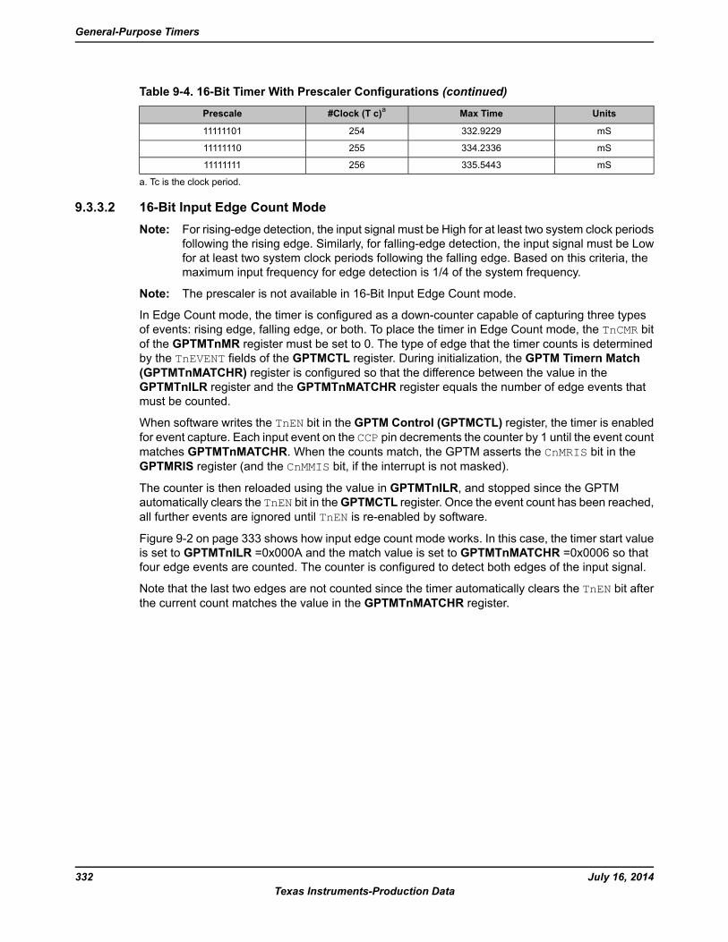
Table 9-4. 16-Bit Timer With Prescaler Configurations (continued)
UnitsMax Time#Clock (T c)aPrescale
mS332.922925411111101
mS334.233625511111110
mS335.544325611111111
a. Tc is the clock period.
9.3.3.2 16-Bit Input Edge Count ModeNote: For rising-edge detection, the input signal must be High for at least two system clock periods
following the rising edge. Similarly, for falling-edge detection, the input signal must be Lowfor at least two system clock periods following the falling edge. Based on this criteria, themaximum input frequency for edge detection is 1/4 of the system frequency.
Note: The prescaler is not available in 16-Bit Input Edge Count mode.
In Edge Count mode, the timer is configured as a down-counter capable of capturing three typesof events: rising edge, falling edge, or both. To place the timer in Edge Count mode, the TnCMR bitof the GPTMTnMR register must be set to 0. The type of edge that the timer counts is determinedby the TnEVENT fields of the GPTMCTL register. During initialization, the GPTM Timern Match(GPTMTnMATCHR) register is configured so that the difference between the value in theGPTMTnILR register and the GPTMTnMATCHR register equals the number of edge events thatmust be counted.
When software writes the TnEN bit in the GPTM Control (GPTMCTL) register, the timer is enabledfor event capture. Each input event on the CCP pin decrements the counter by 1 until the event countmatches GPTMTnMATCHR. When the counts match, the GPTM asserts the CnMRIS bit in theGPTMRIS register (and the CnMMIS bit, if the interrupt is not masked).
The counter is then reloaded using the value in GPTMTnILR, and stopped since the GPTMautomatically clears the TnEN bit in theGPTMCTL register. Once the event count has been reached,all further events are ignored until TnEN is re-enabled by software.
Figure 9-2 on page 333 shows how input edge count mode works. In this case, the timer start valueis set to GPTMTnILR =0x000A and the match value is set to GPTMTnMATCHR =0x0006 so thatfour edge events are counted. The counter is configured to detect both edges of the input signal.
Note that the last two edges are not counted since the timer automatically clears the TnEN bit afterthe current count matches the value in the GPTMTnMATCHR register.
July 16, 2014332Texas Instruments-Production Data
General-Purpose Timers
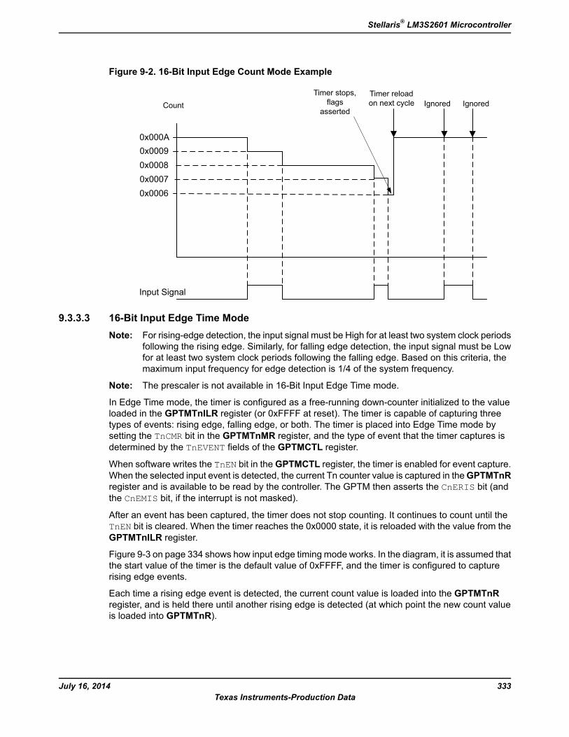
Figure 9-2. 16-Bit Input Edge Count Mode Example
Input Signal
Timer stops,flags
asserted
Timer reloadon next cycle Ignored IgnoredCount
0x000A
0x00060x00070x00080x0009
9.3.3.3 16-Bit Input Edge Time ModeNote: For rising-edge detection, the input signal must be High for at least two system clock periods
following the rising edge. Similarly, for falling edge detection, the input signal must be Lowfor at least two system clock periods following the falling edge. Based on this criteria, themaximum input frequency for edge detection is 1/4 of the system frequency.
Note: The prescaler is not available in 16-Bit Input Edge Time mode.
In Edge Time mode, the timer is configured as a free-running down-counter initialized to the valueloaded in the GPTMTnILR register (or 0xFFFF at reset). The timer is capable of capturing threetypes of events: rising edge, falling edge, or both. The timer is placed into Edge Time mode bysetting the TnCMR bit in the GPTMTnMR register, and the type of event that the timer captures isdetermined by the TnEVENT fields of the GPTMCTL register.
When software writes the TnEN bit in theGPTMCTL register, the timer is enabled for event capture.When the selected input event is detected, the current Tn counter value is captured in theGPTMTnRregister and is available to be read by the controller. The GPTM then asserts the CnERIS bit (andthe CnEMIS bit, if the interrupt is not masked).
After an event has been captured, the timer does not stop counting. It continues to count until theTnEN bit is cleared. When the timer reaches the 0x0000 state, it is reloaded with the value from theGPTMTnILR register.
Figure 9-3 on page 334 shows how input edge timing mode works. In the diagram, it is assumed thatthe start value of the timer is the default value of 0xFFFF, and the timer is configured to capturerising edge events.
Each time a rising edge event is detected, the current count value is loaded into the GPTMTnRregister, and is held there until another rising edge is detected (at which point the new count valueis loaded into GPTMTnR).
333July 16, 2014Texas Instruments-Production Data
Stellaris® LM3S2601 Microcontroller
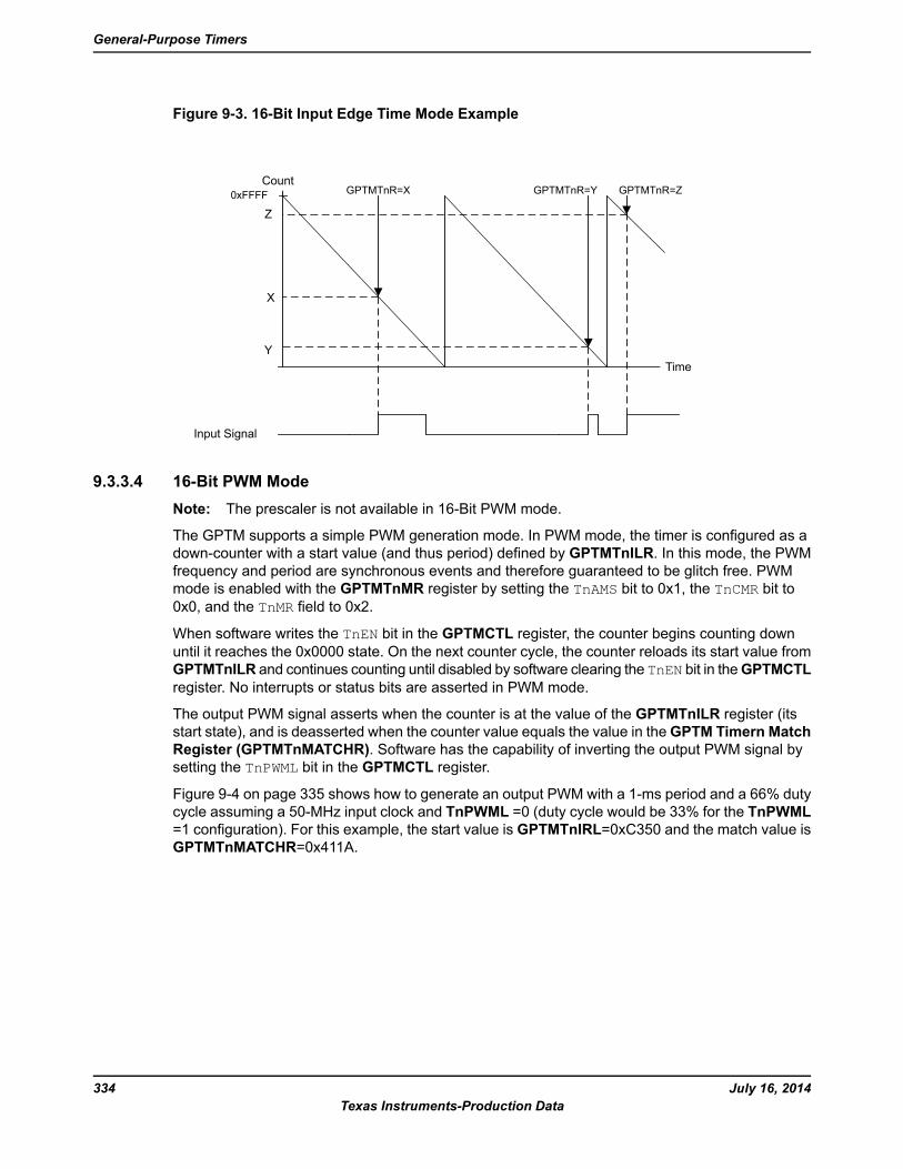
Figure 9-3. 16-Bit Input Edge Time Mode Example
GPTMTnR=Y
Input Signal
Time
CountGPTMTnR=X GPTMTnR=Z
Z
X
Y
0xFFFF
9.3.3.4 16-Bit PWM ModeNote: The prescaler is not available in 16-Bit PWM mode.
The GPTM supports a simple PWM generation mode. In PWM mode, the timer is configured as adown-counter with a start value (and thus period) defined by GPTMTnILR. In this mode, the PWMfrequency and period are synchronous events and therefore guaranteed to be glitch free. PWMmode is enabled with the GPTMTnMR register by setting the TnAMS bit to 0x1, the TnCMR bit to0x0, and the TnMR field to 0x2.
When software writes the TnEN bit in the GPTMCTL register, the counter begins counting downuntil it reaches the 0x0000 state. On the next counter cycle, the counter reloads its start value fromGPTMTnILR and continues counting until disabled by software clearing the TnEN bit in theGPTMCTLregister. No interrupts or status bits are asserted in PWM mode.
The output PWM signal asserts when the counter is at the value of the GPTMTnILR register (itsstart state), and is deasserted when the counter value equals the value in theGPTM Timern MatchRegister (GPTMTnMATCHR). Software has the capability of inverting the output PWM signal bysetting the TnPWML bit in the GPTMCTL register.
Figure 9-4 on page 335 shows how to generate an output PWM with a 1-ms period and a 66% dutycycle assuming a 50-MHz input clock and TnPWML =0 (duty cycle would be 33% for the TnPWML=1 configuration). For this example, the start value is GPTMTnIRL=0xC350 and the match value isGPTMTnMATCHR=0x411A.
July 16, 2014334Texas Instruments-Production Data
General-Purpose Timers
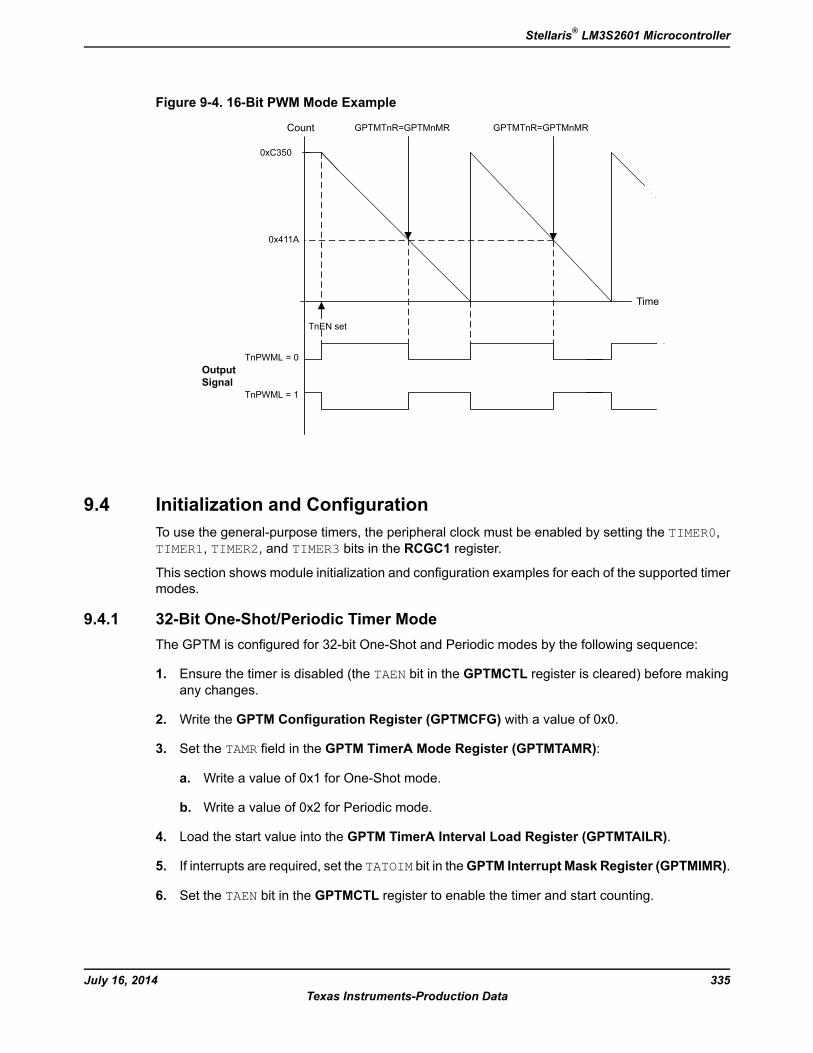
Figure 9-4. 16-Bit PWM Mode Example
OutputSignal
Time
Count GPTMTnR=GPTMnMR GPTMTnR=GPTMnMR
0xC350
0x411A
TnPWML = 0
TnPWML = 1
TnEN set
9.4 Initialization and ConfigurationTo use the general-purpose timers, the peripheral clock must be enabled by setting the TIMER0,TIMER1, TIMER2, and TIMER3 bits in the RCGC1 register.
This section shows module initialization and configuration examples for each of the supported timermodes.
9.4.1 32-Bit One-Shot/Periodic Timer ModeThe GPTM is configured for 32-bit One-Shot and Periodic modes by the following sequence:
1. Ensure the timer is disabled (the TAEN bit in the GPTMCTL register is cleared) before makingany changes.
2. Write the GPTM Configuration Register (GPTMCFG) with a value of 0x0.
3. Set the TAMR field in the GPTM TimerA Mode Register (GPTMTAMR):
a. Write a value of 0x1 for One-Shot mode.
b. Write a value of 0x2 for Periodic mode.
4. Load the start value into the GPTM TimerA Interval Load Register (GPTMTAILR).
5. If interrupts are required, set the TATOIM bit in theGPTM Interrupt Mask Register (GPTMIMR).
6. Set the TAEN bit in the GPTMCTL register to enable the timer and start counting.
335July 16, 2014Texas Instruments-Production Data
Stellaris® LM3S2601 Microcontroller
7. Poll the TATORIS bit in theGPTMRIS register or wait for the interrupt to be generated (if enabled).In both cases, the status flags are cleared by writing a 1 to the TATOCINT bit of the GPTMInterrupt Clear Register (GPTMICR).
In One-Shot mode, the timer stops counting after step 7 on page 336. To re-enable the timer, repeatthe sequence. A timer configured in Periodic mode does not stop counting after it times out.
9.4.2 32-Bit Real-Time Clock (RTC) ModeTo use the RTC mode, the timer must have a 32.768-KHz input signal on an even CCP input. Toenable the RTC feature, follow these steps:
1. Ensure the timer is disabled (the TAEN bit is cleared) before making any changes.
2. Write the GPTM Configuration Register (GPTMCFG) with a value of 0x1.
3. Write the desired match value to the GPTM TimerA Match Register (GPTMTAMATCHR).
4. Set/clear the RTCEN bit in the GPTM Control Register (GPTMCTL) as desired.
5. If interrupts are required, set the RTCIM bit in theGPTM Interrupt Mask Register (GPTMIMR).
6. Set the TAEN bit in the GPTMCTL register to enable the timer and start counting.
When the timer count equals the value in the GPTMTAMATCHR register, the GPTM asserts theRTCRIS bit in theGPTMRIS register and continues counting until Timer A is disabled or a hardwarereset. The interrupt is cleared by writing the RTCCINT bit in the GPTMICR register.
9.4.3 16-Bit One-Shot/Periodic Timer ModeA timer is configured for 16-bit One-Shot and Periodic modes by the following sequence:
1. Ensure the timer is disabled (the TnEN bit is cleared) before making any changes.
2. Write the GPTM Configuration Register (GPTMCFG) with a value of 0x4.
3. Set the TnMR field in the GPTM Timer Mode (GPTMTnMR) register:
a. Write a value of 0x1 for One-Shot mode.
b. Write a value of 0x2 for Periodic mode.
4. If a prescaler is to be used, write the prescale value to the GPTM Timern Prescale Register(GPTMTnPR).
5. Load the start value into the GPTM Timer Interval Load Register (GPTMTnILR).
6. If interrupts are required, set the TnTOIM bit in theGPTM Interrupt Mask Register (GPTMIMR).
7. Set the TnEN bit in the GPTM Control Register (GPTMCTL) to enable the timer and startcounting.
8. Poll the TnTORIS bit in theGPTMRIS register or wait for the interrupt to be generated (if enabled).In both cases, the status flags are cleared by writing a 1 to the TnTOCINT bit of the GPTMInterrupt Clear Register (GPTMICR).
July 16, 2014336Texas Instruments-Production Data
General-Purpose Timers
In One-Shot mode, the timer stops counting after step 8 on page 336. To re-enable the timer, repeatthe sequence. A timer configured in Periodic mode does not stop counting after it times out.
9.4.4 16-Bit Input Edge Count ModeA timer is configured to Input Edge Count mode by the following sequence:
1. Ensure the timer is disabled (the TnEN bit is cleared) before making any changes.
2. Write the GPTM Configuration (GPTMCFG) register with a value of 0x4.
3. In the GPTM Timer Mode (GPTMTnMR) register, write the TnCMR field to 0x0 and the TnMRfield to 0x3.
4. Configure the type of event(s) that the timer captures by writing the TnEVENT field of the GPTMControl (GPTMCTL) register.
5. Load the timer start value into the GPTM Timern Interval Load (GPTMTnILR) register.
6. Load the desired event count into the GPTM Timern Match (GPTMTnMATCHR) register.
7. If interrupts are required, set the CnMIM bit in the GPTM Interrupt Mask (GPTMIMR) register.
8. Set the TnEN bit in theGPTMCTL register to enable the timer and begin waiting for edge events.
9. Poll the CnMRIS bit in theGPTMRIS register or wait for the interrupt to be generated (if enabled).In both cases, the status flags are cleared by writing a 1 to the CnMCINT bit of the GPTMInterrupt Clear (GPTMICR) register.
In Input Edge Count Mode, the timer stops after the desired number of edge events has beendetected. To re-enable the timer, ensure that the TnEN bit is cleared and repeat step 4 on page 337through step 9 on page 337.
9.4.5 16-Bit Input Edge Timing ModeA timer is configured to Input Edge Timing mode by the following sequence:
1. Ensure the timer is disabled (the TnEN bit is cleared) before making any changes.
2. Write the GPTM Configuration (GPTMCFG) register with a value of 0x4.
3. In the GPTM Timer Mode (GPTMTnMR) register, write the TnCMR field to 0x1 and the TnMRfield to 0x3.
4. Configure the type of event that the timer captures by writing the TnEVENT field of the GPTMControl (GPTMCTL) register.
5. Load the timer start value into the GPTM Timern Interval Load (GPTMTnILR) register.
6. If interrupts are required, set the CnEIM bit in the GPTM Interrupt Mask (GPTMIMR) register.
7. Set the TnEN bit in theGPTMControl (GPTMCTL) register to enable the timer and start counting.
8. Poll the CnERIS bit in theGPTMRIS register or wait for the interrupt to be generated (if enabled).In both cases, the status flags are cleared by writing a 1 to the CnECINT bit of the GPTM
337July 16, 2014Texas Instruments-Production Data
Stellaris® LM3S2601 Microcontroller
Interrupt Clear (GPTMICR) register. The time at which the event happened can be obtainedby reading the GPTM Timern (GPTMTnR) register.
In Input Edge Timing mode, the timer continues running after an edge event has been detected,but the timer interval can be changed at any time by writing the GPTMTnILR register. The changetakes effect at the next cycle after the write.
9.4.6 16-Bit PWM ModeA timer is configured to PWM mode using the following sequence:
1. Ensure the timer is disabled (the TnEN bit is cleared) before making any changes.
2. Write the GPTM Configuration (GPTMCFG) register with a value of 0x4.
3. In the GPTM Timer Mode (GPTMTnMR) register, set the TnAMS bit to 0x1, the TnCMR bit to0x0, and the TnMR field to 0x2.
4. Configure the output state of the PWM signal (whether or not it is inverted) in the TnPWML fieldof the GPTM Control (GPTMCTL) register.
5. Load the timer start value into the GPTM Timern Interval Load (GPTMTnILR) register.
6. Load the GPTM Timern Match (GPTMTnMATCHR) register with the desired value.
7. Set the TnEN bit in the GPTM Control (GPTMCTL) register to enable the timer and begingeneration of the output PWM signal.
In PWM Timing mode, the timer continues running after the PWM signal has been generated. ThePWM period can be adjusted at any time by writing the GPTMTnILR register, and the change takeseffect at the next cycle after the write.
9.5 Register MapTable 9-5 on page 338 lists the GPTM registers. The offset listed is a hexadecimal increment to theregister’s address, relative to that timer’s base address:
Timer0: 0x4003.0000 Timer1: 0x4003.1000 Timer2: 0x4003.2000 Timer3: 0x4003.3000
Note that the Timer module clock must be enabled before the registers can be programmed (seepage 212). There must be a delay of 3 system clocks after the Timer module clock is enabled beforeany Timer module registers are accessed.
Table 9-5. Timers Register Map
SeepageDescriptionResetTypeNameOffset
340GPTM Configuration0x0000.0000R/WGPTMCFG0x000
341GPTM TimerA Mode0x0000.0000R/WGPTMTAMR0x004
343GPTM TimerB Mode0x0000.0000R/WGPTMTBMR0x008
July 16, 2014338Texas Instruments-Production Data
General-Purpose Timers
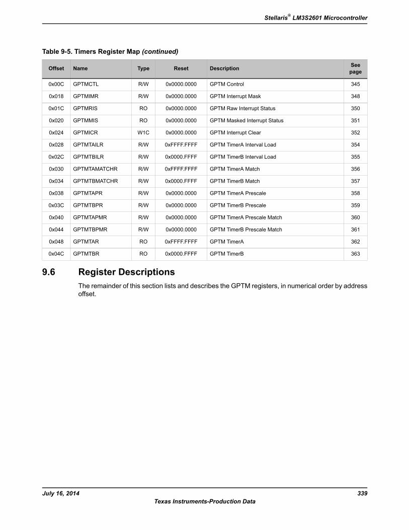
Table 9-5. Timers Register Map (continued)
SeepageDescriptionResetTypeNameOffset
345GPTM Control0x0000.0000R/WGPTMCTL0x00C
348GPTM Interrupt Mask0x0000.0000R/WGPTMIMR0x018
350GPTM Raw Interrupt Status0x0000.0000ROGPTMRIS0x01C
351GPTM Masked Interrupt Status0x0000.0000ROGPTMMIS0x020
352GPTM Interrupt Clear0x0000.0000W1CGPTMICR0x024
354GPTM TimerA Interval Load0xFFFF.FFFFR/WGPTMTAILR0x028
355GPTM TimerB Interval Load0x0000.FFFFR/WGPTMTBILR0x02C
356GPTM TimerA Match0xFFFF.FFFFR/WGPTMTAMATCHR0x030
357GPTM TimerB Match0x0000.FFFFR/WGPTMTBMATCHR0x034
358GPTM TimerA Prescale0x0000.0000R/WGPTMTAPR0x038
359GPTM TimerB Prescale0x0000.0000R/WGPTMTBPR0x03C
360GPTM TimerA Prescale Match0x0000.0000R/WGPTMTAPMR0x040
361GPTM TimerB Prescale Match0x0000.0000R/WGPTMTBPMR0x044
362GPTM TimerA0xFFFF.FFFFROGPTMTAR0x048
363GPTM TimerB0x0000.FFFFROGPTMTBR0x04C
9.6 Register DescriptionsThe remainder of this section lists and describes the GPTM registers, in numerical order by addressoffset.
339July 16, 2014Texas Instruments-Production Data
Stellaris® LM3S2601 Microcontroller
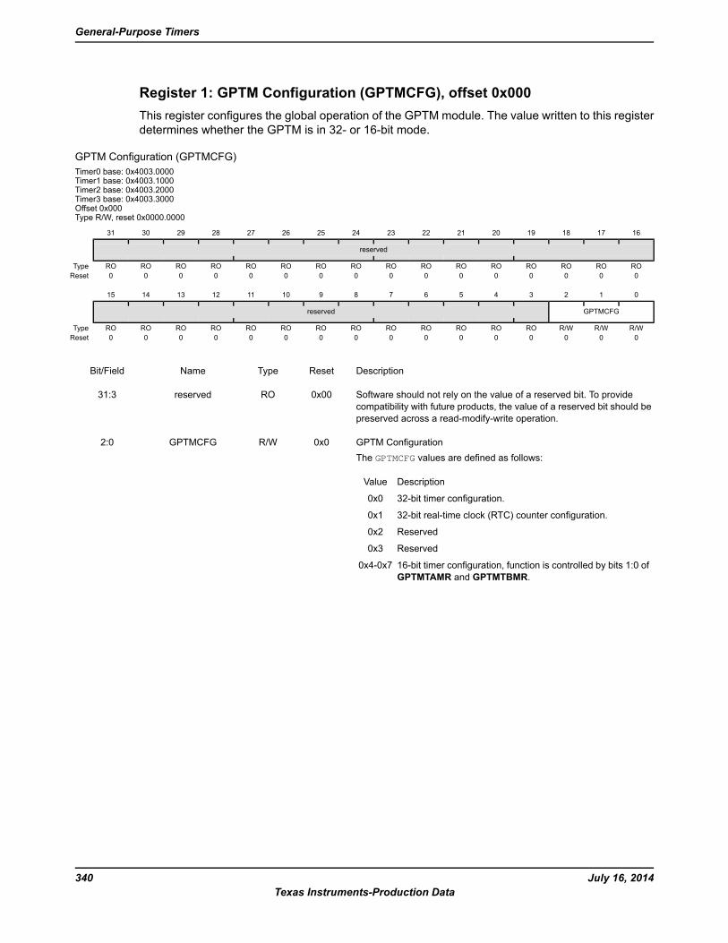
Register 1: GPTM Configuration (GPTMCFG), offset 0x000This register configures the global operation of the GPTM module. The value written to this registerdetermines whether the GPTM is in 32- or 16-bit mode.
GPTM Configuration (GPTMCFG)Timer0 base: 0x4003.0000Timer1 base: 0x4003.1000Timer2 base: 0x4003.2000Timer3 base: 0x4003.3000Offset 0x000Type R/W, reset 0x0000.0000
16171819202122232425262728293031
reserved
ROROROROROROROROROROROROROROROROType0000000000000000Reset
0123456789101112131415
GPTMCFGreserved
R/WR/WR/WROROROROROROROROROROROROROType0000000000000000Reset
DescriptionResetTypeNameBit/Field
Software should not rely on the value of a reserved bit. To providecompatibility with future products, the value of a reserved bit should bepreserved across a read-modify-write operation.
0x00ROreserved31:3
GPTM ConfigurationThe GPTMCFG values are defined as follows:
DescriptionValue
32-bit timer configuration.0x0
32-bit real-time clock (RTC) counter configuration.0x1
Reserved0x2
Reserved0x3
16-bit timer configuration, function is controlled by bits 1:0 ofGPTMTAMR and GPTMTBMR.
0x4-0x7
0x0R/WGPTMCFG2:0
July 16, 2014340Texas Instruments-Production Data
General-Purpose Timers

Register 2: GPTM TimerA Mode (GPTMTAMR), offset 0x004This register configures the GPTM based on the configuration selected in the GPTMCFG register.When in 16-bit PWM mode, set the TAAMS bit to 0x1, the TACMR bit to 0x0, and the TAMR field to0x2.
GPTM TimerA Mode (GPTMTAMR)Timer0 base: 0x4003.0000Timer1 base: 0x4003.1000Timer2 base: 0x4003.2000Timer3 base: 0x4003.3000Offset 0x004Type R/W, reset 0x0000.0000
16171819202122232425262728293031
reserved
ROROROROROROROROROROROROROROROROType0000000000000000Reset
0123456789101112131415
TAMRTACMRTAAMSreserved
R/WR/WR/WR/WROROROROROROROROROROROROType0000000000000000Reset
DescriptionResetTypeNameBit/Field
Software should not rely on the value of a reserved bit. To providecompatibility with future products, the value of a reserved bit should bepreserved across a read-modify-write operation.
0x00ROreserved31:4
GPTM TimerA Alternate Mode SelectThe TAAMS values are defined as follows:
DescriptionValue
Capture mode is enabled.0
PWM mode is enabled.1
Note: To enable PWMmode, youmust also clear the TACMRbit and set the TAMR field to 0x2.
0R/WTAAMS3
GPTM TimerA Capture ModeThe TACMR values are defined as follows:
DescriptionValue
Edge-Count mode0
Edge-Time mode1
0R/WTACMR2
341July 16, 2014Texas Instruments-Production Data
Stellaris® LM3S2601 Microcontroller
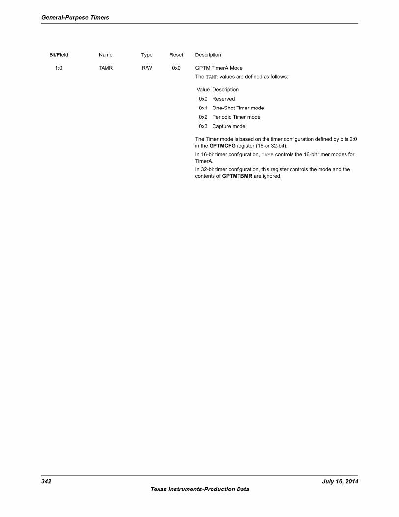
DescriptionResetTypeNameBit/Field
GPTM TimerA ModeThe TAMR values are defined as follows:
DescriptionValue
Reserved0x0
One-Shot Timer mode0x1
Periodic Timer mode0x2
Capture mode0x3
The Timer mode is based on the timer configuration defined by bits 2:0in the GPTMCFG register (16-or 32-bit).In 16-bit timer configuration, TAMR controls the 16-bit timer modes forTimerA.In 32-bit timer configuration, this register controls the mode and thecontents of GPTMTBMR are ignored.
0x0R/WTAMR1:0
July 16, 2014342Texas Instruments-Production Data
General-Purpose Timers
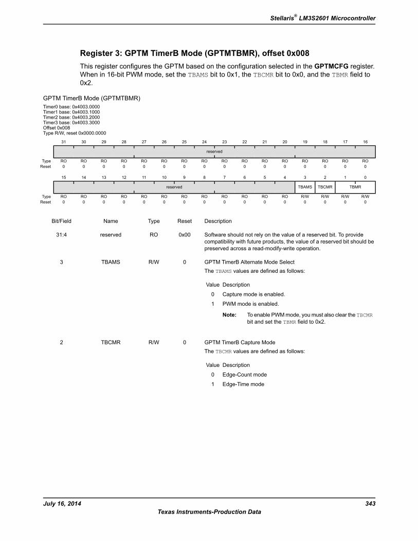
Register 3: GPTM TimerB Mode (GPTMTBMR), offset 0x008This register configures the GPTM based on the configuration selected in the GPTMCFG register.When in 16-bit PWM mode, set the TBAMS bit to 0x1, the TBCMR bit to 0x0, and the TBMR field to0x2.
GPTM TimerB Mode (GPTMTBMR)Timer0 base: 0x4003.0000Timer1 base: 0x4003.1000Timer2 base: 0x4003.2000Timer3 base: 0x4003.3000Offset 0x008Type R/W, reset 0x0000.0000
16171819202122232425262728293031
reserved
ROROROROROROROROROROROROROROROROType0000000000000000Reset
0123456789101112131415
TBMRTBCMRTBAMSreserved
R/WR/WR/WR/WROROROROROROROROROROROROType0000000000000000Reset
DescriptionResetTypeNameBit/Field
Software should not rely on the value of a reserved bit. To providecompatibility with future products, the value of a reserved bit should bepreserved across a read-modify-write operation.
0x00ROreserved31:4
GPTM TimerB Alternate Mode SelectThe TBAMS values are defined as follows:
DescriptionValue
Capture mode is enabled.0
PWM mode is enabled.1
Note: To enable PWMmode, youmust also clear the TBCMRbit and set the TBMR field to 0x2.
0R/WTBAMS3
GPTM TimerB Capture ModeThe TBCMR values are defined as follows:
DescriptionValue
Edge-Count mode0
Edge-Time mode1
0R/WTBCMR2
343July 16, 2014Texas Instruments-Production Data
Stellaris® LM3S2601 Microcontroller
DescriptionResetTypeNameBit/Field
GPTM TimerB ModeThe TBMR values are defined as follows:
DescriptionValue
Reserved0x0
One-Shot Timer mode0x1
Periodic Timer mode0x2
Capture mode0x3
The timer mode is based on the timer configuration defined by bits 2:0in the GPTMCFG register.In 16-bit timer configuration, these bits control the 16-bit timer modesfor TimerB.In 32-bit timer configuration, this register’s contents are ignored andGPTMTAMR is used.
0x0R/WTBMR1:0
July 16, 2014344Texas Instruments-Production Data
General-Purpose Timers
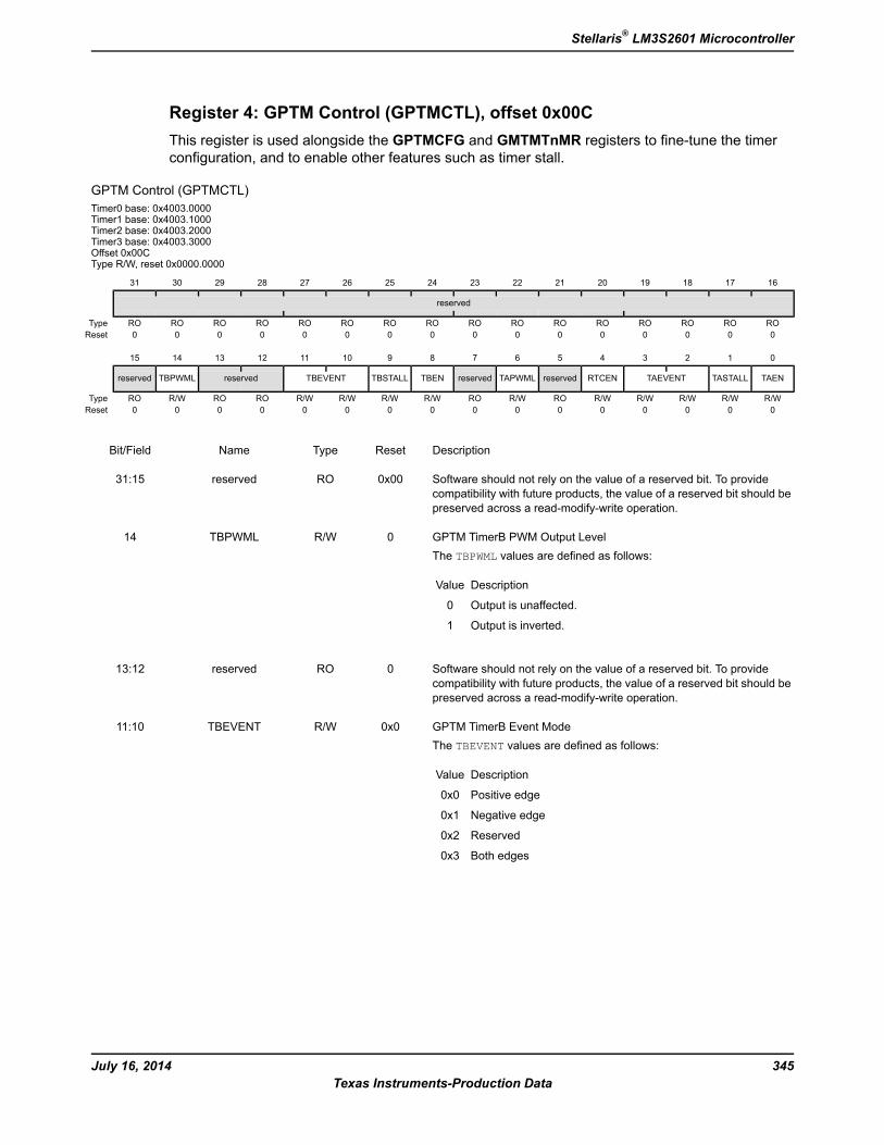
Register 4: GPTM Control (GPTMCTL), offset 0x00CThis register is used alongside the GPTMCFG and GMTMTnMR registers to fine-tune the timerconfiguration, and to enable other features such as timer stall.
GPTM Control (GPTMCTL)Timer0 base: 0x4003.0000Timer1 base: 0x4003.1000Timer2 base: 0x4003.2000Timer3 base: 0x4003.3000Offset 0x00CType R/W, reset 0x0000.0000
16171819202122232425262728293031
reserved
ROROROROROROROROROROROROROROROROType0000000000000000Reset
0123456789101112131415
TAENTASTALLTAEVENTRTCENreservedTAPWMLreservedTBENTBSTALLTBEVENTreservedTBPWMLreserved
R/WR/WR/WR/WR/WROR/WROR/WR/WR/WR/WROROR/WROType0000000000000000Reset
DescriptionResetTypeNameBit/Field
Software should not rely on the value of a reserved bit. To providecompatibility with future products, the value of a reserved bit should bepreserved across a read-modify-write operation.
0x00ROreserved31:15
GPTM TimerB PWM Output LevelThe TBPWML values are defined as follows:
DescriptionValue
Output is unaffected.0
Output is inverted.1
0R/WTBPWML14
Software should not rely on the value of a reserved bit. To providecompatibility with future products, the value of a reserved bit should bepreserved across a read-modify-write operation.
0ROreserved13:12
GPTM TimerB Event ModeThe TBEVENT values are defined as follows:
DescriptionValue
Positive edge0x0
Negative edge0x1
Reserved0x2
Both edges0x3
0x0R/WTBEVENT11:10
345July 16, 2014Texas Instruments-Production Data
Stellaris® LM3S2601 Microcontroller
DescriptionResetTypeNameBit/Field
GPTM Timer B Stall EnableThe TBSTALL values are defined as follows:
DescriptionValue
Timer B continues counting while the processor is halted by thedebugger.
0
Timer B freezes counting while the processor is halted by thedebugger.
1
If the processor is executing normally, the TBSTALL bit is ignored.
0R/WTBSTALL9
GPTM TimerB EnableThe TBEN values are defined as follows:
DescriptionValue
TimerB is disabled.0
TimerB is enabled and begins counting or the capture logic isenabled based on the GPTMCFG register.
1
0R/WTBEN8
Software should not rely on the value of a reserved bit. To providecompatibility with future products, the value of a reserved bit should bepreserved across a read-modify-write operation.
0ROreserved7
GPTM TimerA PWM Output LevelThe TAPWML values are defined as follows:
DescriptionValue
Output is unaffected.0
Output is inverted.1
0R/WTAPWML6
Software should not rely on the value of a reserved bit. To providecompatibility with future products, the value of a reserved bit should bepreserved across a read-modify-write operation.
0ROreserved5
GPTM RTC EnableThe RTCEN values are defined as follows:
DescriptionValue
RTC counting is disabled.0
RTC counting is enabled.1
0R/WRTCEN4
GPTM TimerA Event ModeThe TAEVENT values are defined as follows:
DescriptionValue
Positive edge0x0
Negative edge0x1
Reserved0x2
Both edges0x3
0x0R/WTAEVENT3:2
July 16, 2014346Texas Instruments-Production Data
General-Purpose Timers
DescriptionResetTypeNameBit/Field
GPTM Timer A Stall EnableThe TASTALL values are defined as follows:
DescriptionValue
Timer A continues counting while the processor is halted by thedebugger.
0
Timer A freezes counting while the processor is halted by thedebugger.
1
If the processor is executing normally, the TASTALL bit is ignored.
0R/WTASTALL1
GPTM TimerA EnableThe TAEN values are defined as follows:
DescriptionValue
TimerA is disabled.0
TimerA is enabled and begins counting or the capture logic isenabled based on the GPTMCFG register.
1
0R/WTAEN0
347July 16, 2014Texas Instruments-Production Data
Stellaris® LM3S2601 Microcontroller
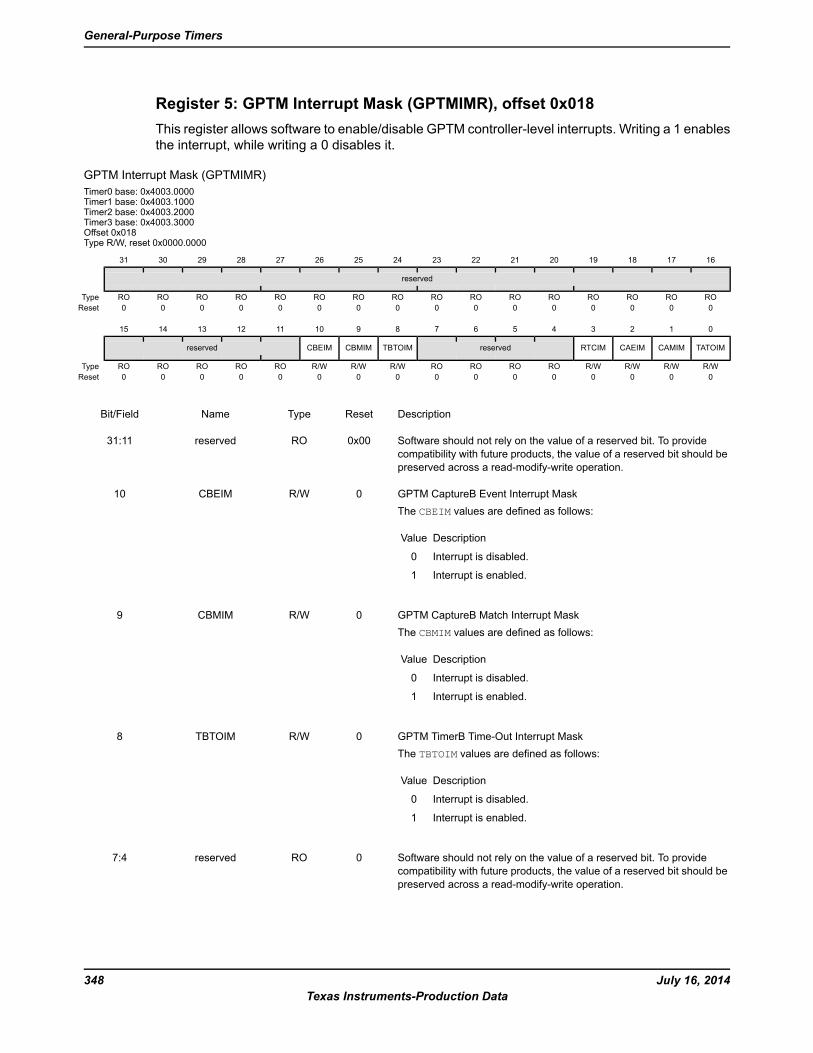
Register 5: GPTM Interrupt Mask (GPTMIMR), offset 0x018This register allows software to enable/disable GPTM controller-level interrupts. Writing a 1 enablesthe interrupt, while writing a 0 disables it.
GPTM Interrupt Mask (GPTMIMR)Timer0 base: 0x4003.0000Timer1 base: 0x4003.1000Timer2 base: 0x4003.2000Timer3 base: 0x4003.3000Offset 0x018Type R/W, reset 0x0000.0000
16171819202122232425262728293031
reserved
ROROROROROROROROROROROROROROROROType0000000000000000Reset
0123456789101112131415
TATOIMCAMIMCAEIMRTCIMreservedTBTOIMCBMIMCBEIMreserved
R/WR/WR/WR/WROROROROR/WR/WR/WROROROROROType0000000000000000Reset
DescriptionResetTypeNameBit/Field
Software should not rely on the value of a reserved bit. To providecompatibility with future products, the value of a reserved bit should bepreserved across a read-modify-write operation.
0x00ROreserved31:11
GPTM CaptureB Event Interrupt MaskThe CBEIM values are defined as follows:
DescriptionValue
Interrupt is disabled.0
Interrupt is enabled.1
0R/WCBEIM10
GPTM CaptureB Match Interrupt MaskThe CBMIM values are defined as follows:
DescriptionValue
Interrupt is disabled.0
Interrupt is enabled.1
0R/WCBMIM9
GPTM TimerB Time-Out Interrupt MaskThe TBTOIM values are defined as follows:
DescriptionValue
Interrupt is disabled.0
Interrupt is enabled.1
0R/WTBTOIM8
Software should not rely on the value of a reserved bit. To providecompatibility with future products, the value of a reserved bit should bepreserved across a read-modify-write operation.
0ROreserved7:4
July 16, 2014348Texas Instruments-Production Data
General-Purpose Timers
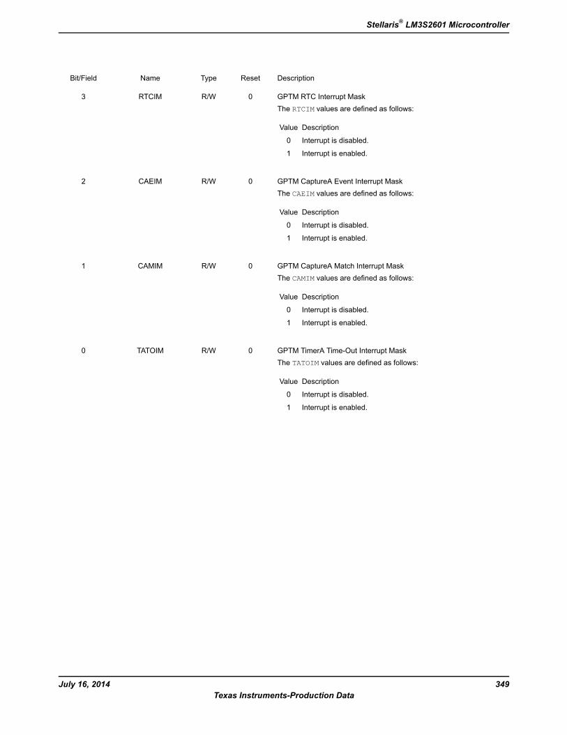
DescriptionResetTypeNameBit/Field
GPTM RTC Interrupt MaskThe RTCIM values are defined as follows:
DescriptionValue
Interrupt is disabled.0
Interrupt is enabled.1
0R/WRTCIM3
GPTM CaptureA Event Interrupt MaskThe CAEIM values are defined as follows:
DescriptionValue
Interrupt is disabled.0
Interrupt is enabled.1
0R/WCAEIM2
GPTM CaptureA Match Interrupt MaskThe CAMIM values are defined as follows:
DescriptionValue
Interrupt is disabled.0
Interrupt is enabled.1
0R/WCAMIM1
GPTM TimerA Time-Out Interrupt MaskThe TATOIM values are defined as follows:
DescriptionValue
Interrupt is disabled.0
Interrupt is enabled.1
0R/WTATOIM0
349July 16, 2014Texas Instruments-Production Data
Stellaris® LM3S2601 Microcontroller
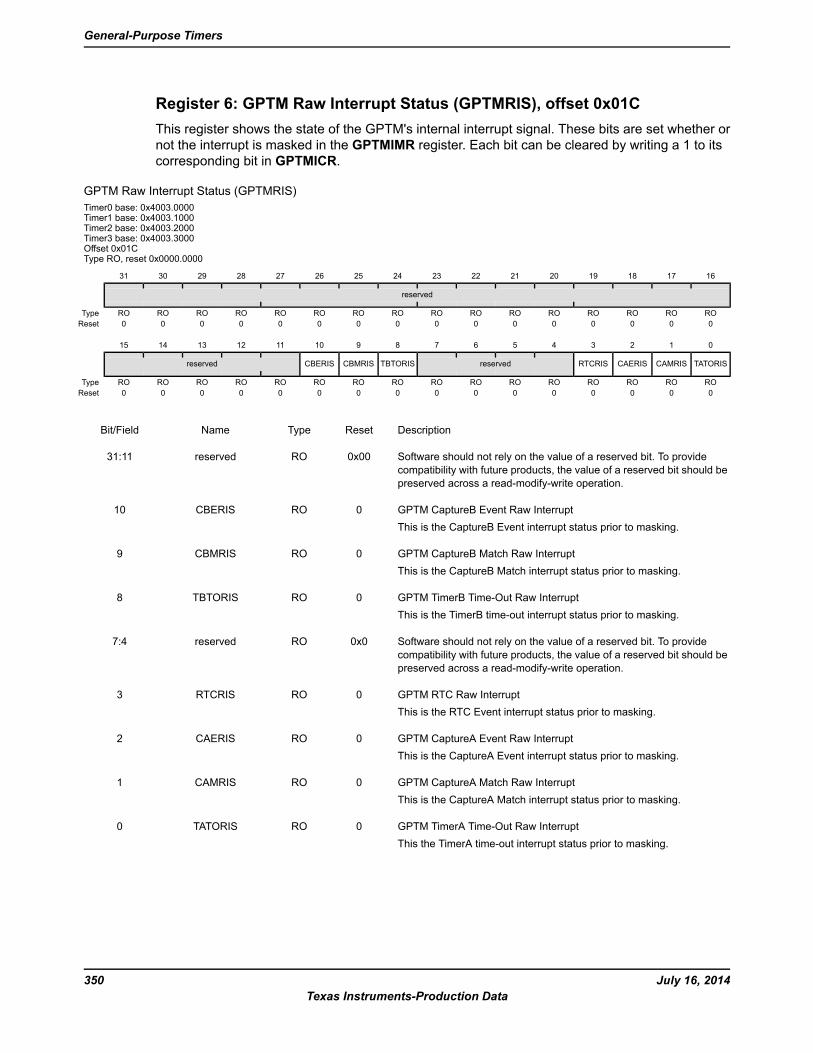
Register 6: GPTM Raw Interrupt Status (GPTMRIS), offset 0x01CThis register shows the state of the GPTM's internal interrupt signal. These bits are set whether ornot the interrupt is masked in the GPTMIMR register. Each bit can be cleared by writing a 1 to itscorresponding bit in GPTMICR.
GPTM Raw Interrupt Status (GPTMRIS)Timer0 base: 0x4003.0000Timer1 base: 0x4003.1000Timer2 base: 0x4003.2000Timer3 base: 0x4003.3000Offset 0x01CType RO, reset 0x0000.0000
16171819202122232425262728293031
reserved
ROROROROROROROROROROROROROROROROType0000000000000000Reset
0123456789101112131415
TATORISCAMRISCAERISRTCRISreservedTBTORISCBMRISCBERISreserved
ROROROROROROROROROROROROROROROROType0000000000000000Reset
DescriptionResetTypeNameBit/Field
Software should not rely on the value of a reserved bit. To providecompatibility with future products, the value of a reserved bit should bepreserved across a read-modify-write operation.
0x00ROreserved31:11
GPTM CaptureB Event Raw InterruptThis is the CaptureB Event interrupt status prior to masking.
0ROCBERIS10
GPTM CaptureB Match Raw InterruptThis is the CaptureB Match interrupt status prior to masking.
0ROCBMRIS9
GPTM TimerB Time-Out Raw InterruptThis is the TimerB time-out interrupt status prior to masking.
0ROTBTORIS8
Software should not rely on the value of a reserved bit. To providecompatibility with future products, the value of a reserved bit should bepreserved across a read-modify-write operation.
0x0ROreserved7:4
GPTM RTC Raw InterruptThis is the RTC Event interrupt status prior to masking.
0RORTCRIS3
GPTM CaptureA Event Raw InterruptThis is the CaptureA Event interrupt status prior to masking.
0ROCAERIS2
GPTM CaptureA Match Raw InterruptThis is the CaptureA Match interrupt status prior to masking.
0ROCAMRIS1
GPTM TimerA Time-Out Raw InterruptThis the TimerA time-out interrupt status prior to masking.
0ROTATORIS0
July 16, 2014350Texas Instruments-Production Data
General-Purpose Timers
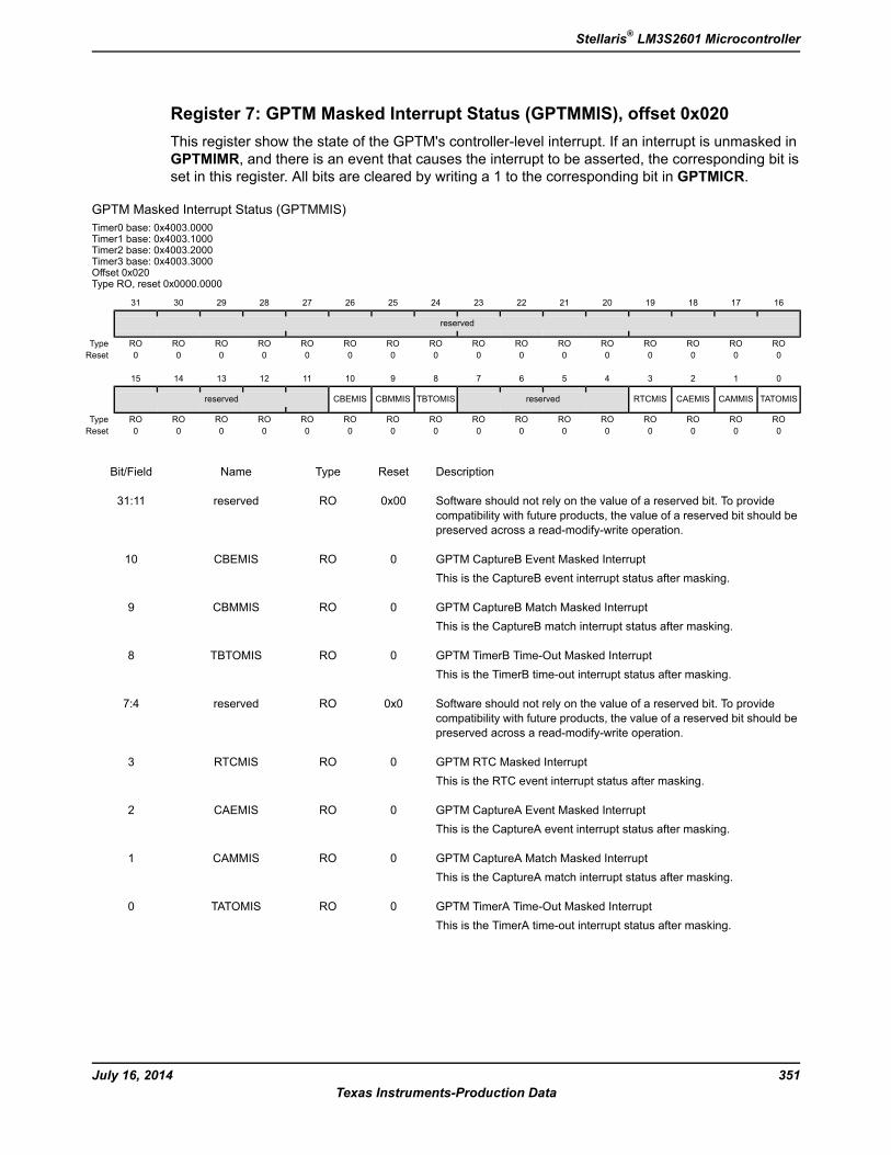
Register 7: GPTM Masked Interrupt Status (GPTMMIS), offset 0x020This register show the state of the GPTM's controller-level interrupt. If an interrupt is unmasked inGPTMIMR, and there is an event that causes the interrupt to be asserted, the corresponding bit isset in this register. All bits are cleared by writing a 1 to the corresponding bit in GPTMICR.
GPTM Masked Interrupt Status (GPTMMIS)Timer0 base: 0x4003.0000Timer1 base: 0x4003.1000Timer2 base: 0x4003.2000Timer3 base: 0x4003.3000Offset 0x020Type RO, reset 0x0000.0000
16171819202122232425262728293031
reserved
ROROROROROROROROROROROROROROROROType0000000000000000Reset
0123456789101112131415
TATOMISCAMMISCAEMISRTCMISreservedTBTOMISCBMMISCBEMISreserved
ROROROROROROROROROROROROROROROROType0000000000000000Reset
DescriptionResetTypeNameBit/Field
Software should not rely on the value of a reserved bit. To providecompatibility with future products, the value of a reserved bit should bepreserved across a read-modify-write operation.
0x00ROreserved31:11
GPTM CaptureB Event Masked InterruptThis is the CaptureB event interrupt status after masking.
0ROCBEMIS10
GPTM CaptureB Match Masked InterruptThis is the CaptureB match interrupt status after masking.
0ROCBMMIS9
GPTM TimerB Time-Out Masked InterruptThis is the TimerB time-out interrupt status after masking.
0ROTBTOMIS8
Software should not rely on the value of a reserved bit. To providecompatibility with future products, the value of a reserved bit should bepreserved across a read-modify-write operation.
0x0ROreserved7:4
GPTM RTC Masked InterruptThis is the RTC event interrupt status after masking.
0RORTCMIS3
GPTM CaptureA Event Masked InterruptThis is the CaptureA event interrupt status after masking.
0ROCAEMIS2
GPTM CaptureA Match Masked InterruptThis is the CaptureA match interrupt status after masking.
0ROCAMMIS1
GPTM TimerA Time-Out Masked InterruptThis is the TimerA time-out interrupt status after masking.
0ROTATOMIS0
351July 16, 2014Texas Instruments-Production Data
Stellaris® LM3S2601 Microcontroller
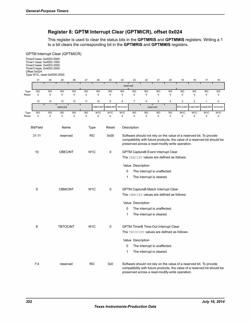
Register 8: GPTM Interrupt Clear (GPTMICR), offset 0x024This register is used to clear the status bits in the GPTMRIS and GPTMMIS registers. Writing a 1to a bit clears the corresponding bit in the GPTMRIS and GPTMMIS registers.
GPTM Interrupt Clear (GPTMICR)Timer0 base: 0x4003.0000Timer1 base: 0x4003.1000Timer2 base: 0x4003.2000Timer3 base: 0x4003.3000Offset 0x024Type W1C, reset 0x0000.0000
16171819202122232425262728293031
reserved
ROROROROROROROROROROROROROROROROType0000000000000000Reset
0123456789101112131415
TATOCINTCAMCINTCAECINTRTCCINTreservedTBTOCINTCBMCINTCBECINTreserved
W1CW1CW1CW1CROROROROW1CW1CW1CROROROROROType0000000000000000Reset
DescriptionResetTypeNameBit/Field
Software should not rely on the value of a reserved bit. To providecompatibility with future products, the value of a reserved bit should bepreserved across a read-modify-write operation.
0x00ROreserved31:11
GPTM CaptureB Event Interrupt ClearThe CBECINT values are defined as follows:
DescriptionValue
The interrupt is unaffected.0
The interrupt is cleared.1
0W1CCBECINT10
GPTM CaptureB Match Interrupt ClearThe CBMCINT values are defined as follows:
DescriptionValue
The interrupt is unaffected.0
The interrupt is cleared.1
0W1CCBMCINT9
GPTM TimerB Time-Out Interrupt ClearThe TBTOCINT values are defined as follows:
DescriptionValue
The interrupt is unaffected.0
The interrupt is cleared.1
0W1CTBTOCINT8
Software should not rely on the value of a reserved bit. To providecompatibility with future products, the value of a reserved bit should bepreserved across a read-modify-write operation.
0x0ROreserved7:4
July 16, 2014352Texas Instruments-Production Data
General-Purpose Timers
DescriptionResetTypeNameBit/Field
GPTM RTC Interrupt ClearThe RTCCINT values are defined as follows:
DescriptionValue
The interrupt is unaffected.0
The interrupt is cleared.1
0W1CRTCCINT3
GPTM CaptureA Event Interrupt ClearThe CAECINT values are defined as follows:
DescriptionValue
The interrupt is unaffected.0
The interrupt is cleared.1
0W1CCAECINT2
GPTM CaptureA Match Interrupt ClearThe CAMCINT values are defined as follows:
DescriptionValue
The interrupt is unaffected.0
The interrupt is cleared.1
0W1CCAMCINT1
GPTM TimerA Time-Out Interrupt ClearThe TATOCINT values are defined as follows:
DescriptionValue
The interrupt is unaffected.0
The interrupt is cleared.1
0W1CTATOCINT0
353July 16, 2014Texas Instruments-Production Data
Stellaris® LM3S2601 Microcontroller
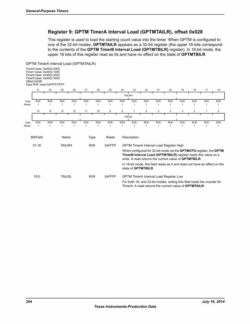
Register 9: GPTM TimerA Interval Load (GPTMTAILR), offset 0x028This register is used to load the starting count value into the timer. When GPTM is configured toone of the 32-bit modes, GPTMTAILR appears as a 32-bit register (the upper 16-bits correspondto the contents of the GPTM TimerB Interval Load (GPTMTBILR) register). In 16-bit mode, theupper 16 bits of this register read as 0s and have no effect on the state of GPTMTBILR.
GPTM TimerA Interval Load (GPTMTAILR)Timer0 base: 0x4003.0000Timer1 base: 0x4003.1000Timer2 base: 0x4003.2000Timer3 base: 0x4003.3000Offset 0x028Type R/W, reset 0xFFFF.FFFF
16171819202122232425262728293031
TAILRH
R/WR/WR/WR/WR/WR/WR/WR/WR/WR/WR/WR/WR/WR/WR/WR/WType1111111111111111Reset
0123456789101112131415
TAILRL
R/WR/WR/WR/WR/WR/WR/WR/WR/WR/WR/WR/WR/WR/WR/WR/WType1111111111111111Reset
DescriptionResetTypeNameBit/Field
GPTM TimerA Interval Load Register HighWhen configured for 32-bit mode via theGPTMCFG register, theGPTMTimerB Interval Load (GPTMTBILR) register loads this value on awrite. A read returns the current value of GPTMTBILR.In 16-bit mode, this field reads as 0 and does not have an effect on thestate of GPTMTBILR.
0xFFFFR/WTAILRH31:16
GPTM TimerA Interval Load Register LowFor both 16- and 32-bit modes, writing this field loads the counter forTimerA. A read returns the current value of GPTMTAILR.
0xFFFFR/WTAILRL15:0
July 16, 2014354Texas Instruments-Production Data
General-Purpose Timers
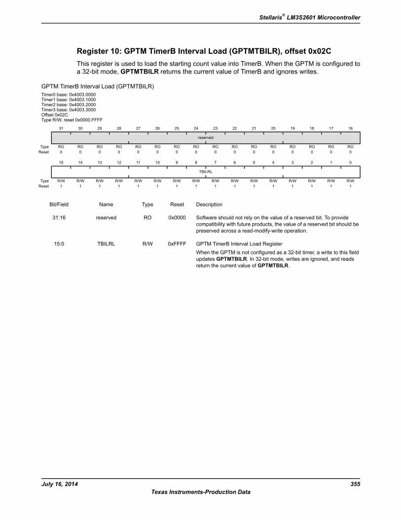
Register 10: GPTM TimerB Interval Load (GPTMTBILR), offset 0x02CThis register is used to load the starting count value into TimerB. When the GPTM is configured toa 32-bit mode, GPTMTBILR returns the current value of TimerB and ignores writes.
GPTM TimerB Interval Load (GPTMTBILR)Timer0 base: 0x4003.0000Timer1 base: 0x4003.1000Timer2 base: 0x4003.2000Timer3 base: 0x4003.3000Offset 0x02CType R/W, reset 0x0000.FFFF
16171819202122232425262728293031
reserved
ROROROROROROROROROROROROROROROROType0000000000000000Reset
0123456789101112131415
TBILRL
R/WR/WR/WR/WR/WR/WR/WR/WR/WR/WR/WR/WR/WR/WR/WR/WType1111111111111111Reset
DescriptionResetTypeNameBit/Field
Software should not rely on the value of a reserved bit. To providecompatibility with future products, the value of a reserved bit should bepreserved across a read-modify-write operation.
0x0000ROreserved31:16
GPTM TimerB Interval Load RegisterWhen the GPTM is not configured as a 32-bit timer, a write to this fieldupdates GPTMTBILR. In 32-bit mode, writes are ignored, and readsreturn the current value of GPTMTBILR.
0xFFFFR/WTBILRL15:0
355July 16, 2014Texas Instruments-Production Data
Stellaris® LM3S2601 Microcontroller
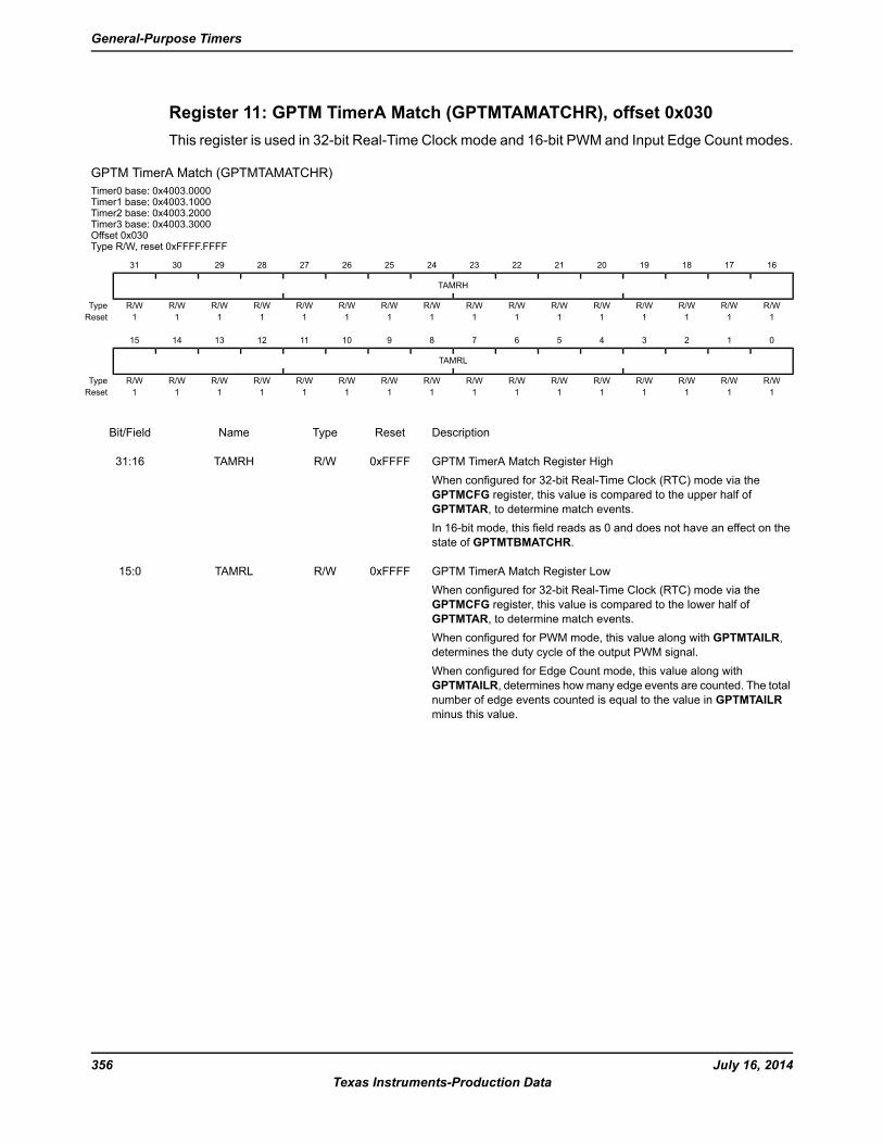
Register 11: GPTM TimerA Match (GPTMTAMATCHR), offset 0x030This register is used in 32-bit Real-Time Clock mode and 16-bit PWM and Input Edge Count modes.
GPTM TimerA Match (GPTMTAMATCHR)Timer0 base: 0x4003.0000Timer1 base: 0x4003.1000Timer2 base: 0x4003.2000Timer3 base: 0x4003.3000Offset 0x030Type R/W, reset 0xFFFF.FFFF
16171819202122232425262728293031
TAMRH
R/WR/WR/WR/WR/WR/WR/WR/WR/WR/WR/WR/WR/WR/WR/WR/WType1111111111111111Reset
0123456789101112131415
TAMRL
R/WR/WR/WR/WR/WR/WR/WR/WR/WR/WR/WR/WR/WR/WR/WR/WType1111111111111111Reset
DescriptionResetTypeNameBit/Field
GPTM TimerA Match Register HighWhen configured for 32-bit Real-Time Clock (RTC) mode via theGPTMCFG register, this value is compared to the upper half ofGPTMTAR, to determine match events.In 16-bit mode, this field reads as 0 and does not have an effect on thestate of GPTMTBMATCHR.
0xFFFFR/WTAMRH31:16
GPTM TimerA Match Register LowWhen configured for 32-bit Real-Time Clock (RTC) mode via theGPTMCFG register, this value is compared to the lower half ofGPTMTAR, to determine match events.When configured for PWM mode, this value along with GPTMTAILR,determines the duty cycle of the output PWM signal.When configured for Edge Count mode, this value along withGPTMTAILR, determines howmany edge events are counted. The totalnumber of edge events counted is equal to the value in GPTMTAILRminus this value.
0xFFFFR/WTAMRL15:0
July 16, 2014356Texas Instruments-Production Data
General-Purpose Timers
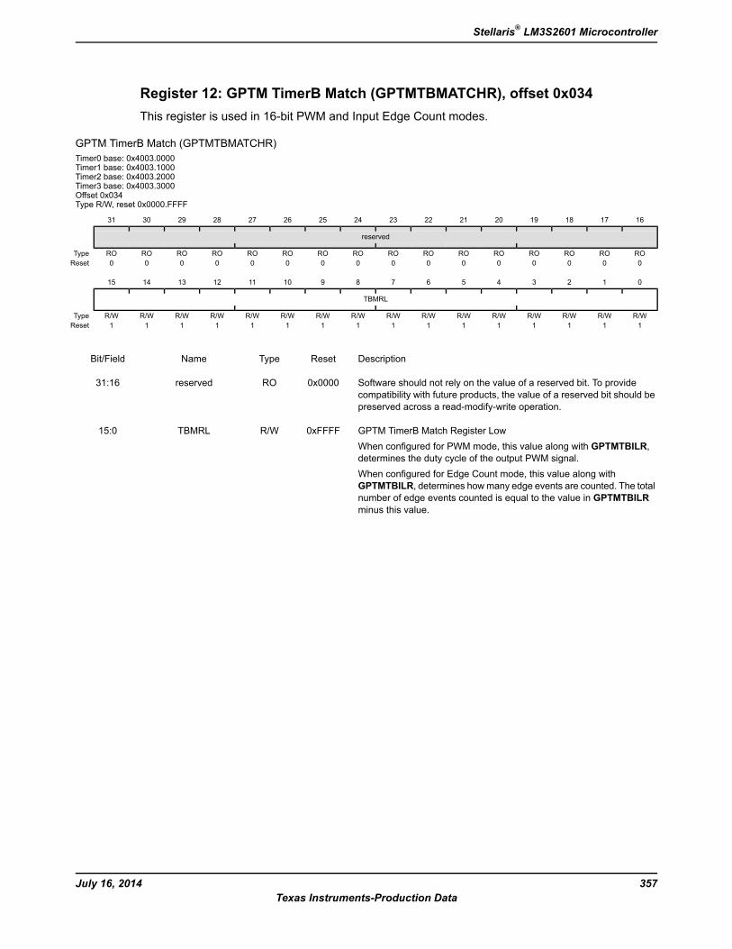
Register 12: GPTM TimerB Match (GPTMTBMATCHR), offset 0x034This register is used in 16-bit PWM and Input Edge Count modes.
GPTM TimerB Match (GPTMTBMATCHR)Timer0 base: 0x4003.0000Timer1 base: 0x4003.1000Timer2 base: 0x4003.2000Timer3 base: 0x4003.3000Offset 0x034Type R/W, reset 0x0000.FFFF
16171819202122232425262728293031
reserved
ROROROROROROROROROROROROROROROROType0000000000000000Reset
0123456789101112131415
TBMRL
R/WR/WR/WR/WR/WR/WR/WR/WR/WR/WR/WR/WR/WR/WR/WR/WType1111111111111111Reset
DescriptionResetTypeNameBit/Field
Software should not rely on the value of a reserved bit. To providecompatibility with future products, the value of a reserved bit should bepreserved across a read-modify-write operation.
0x0000ROreserved31:16
GPTM TimerB Match Register LowWhen configured for PWM mode, this value along with GPTMTBILR,determines the duty cycle of the output PWM signal.When configured for Edge Count mode, this value along withGPTMTBILR, determines howmany edge events are counted. The totalnumber of edge events counted is equal to the value in GPTMTBILRminus this value.
0xFFFFR/WTBMRL15:0
357July 16, 2014Texas Instruments-Production Data
Stellaris® LM3S2601 Microcontroller
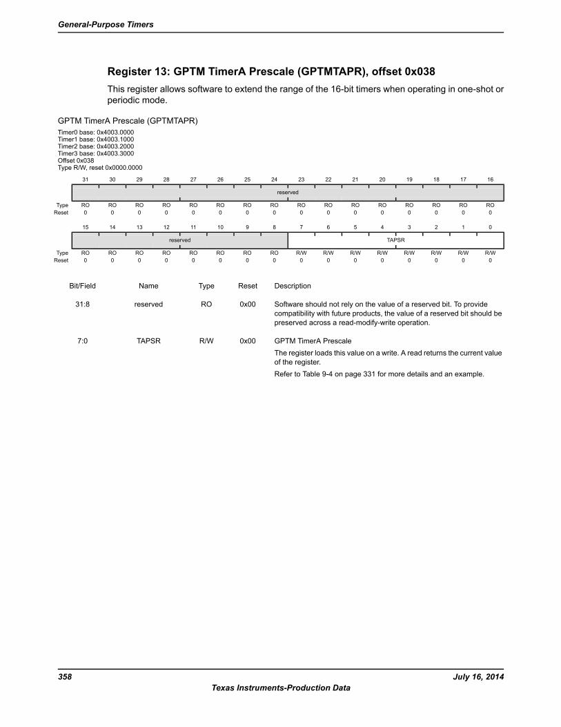
Register 13: GPTM TimerA Prescale (GPTMTAPR), offset 0x038This register allows software to extend the range of the 16-bit timers when operating in one-shot orperiodic mode.
GPTM TimerA Prescale (GPTMTAPR)Timer0 base: 0x4003.0000Timer1 base: 0x4003.1000Timer2 base: 0x4003.2000Timer3 base: 0x4003.3000Offset 0x038Type R/W, reset 0x0000.0000
16171819202122232425262728293031
reserved
ROROROROROROROROROROROROROROROROType0000000000000000Reset
0123456789101112131415
TAPSRreserved
R/WR/WR/WR/WR/WR/WR/WR/WROROROROROROROROType0000000000000000Reset
DescriptionResetTypeNameBit/Field
Software should not rely on the value of a reserved bit. To providecompatibility with future products, the value of a reserved bit should bepreserved across a read-modify-write operation.
0x00ROreserved31:8
GPTM TimerA PrescaleThe register loads this value on a write. A read returns the current valueof the register.Refer to Table 9-4 on page 331 for more details and an example.
0x00R/WTAPSR7:0
July 16, 2014358Texas Instruments-Production Data
General-Purpose Timers
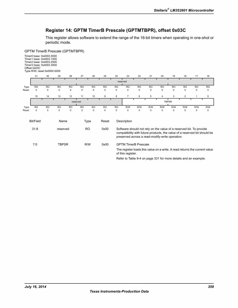
Register 14: GPTM TimerB Prescale (GPTMTBPR), offset 0x03CThis register allows software to extend the range of the 16-bit timers when operating in one-shot orperiodic mode.
GPTM TimerB Prescale (GPTMTBPR)Timer0 base: 0x4003.0000Timer1 base: 0x4003.1000Timer2 base: 0x4003.2000Timer3 base: 0x4003.3000Offset 0x03CType R/W, reset 0x0000.0000
16171819202122232425262728293031
reserved
ROROROROROROROROROROROROROROROROType0000000000000000Reset
0123456789101112131415
TBPSRreserved
R/WR/WR/WR/WR/WR/WR/WR/WROROROROROROROROType0000000000000000Reset
DescriptionResetTypeNameBit/Field
Software should not rely on the value of a reserved bit. To providecompatibility with future products, the value of a reserved bit should bepreserved across a read-modify-write operation.
0x00ROreserved31:8
GPTM TimerB PrescaleThe register loads this value on a write. A read returns the current valueof this register.Refer to Table 9-4 on page 331 for more details and an example.
0x00R/WTBPSR7:0
359July 16, 2014Texas Instruments-Production Data
Stellaris® LM3S2601 Microcontroller
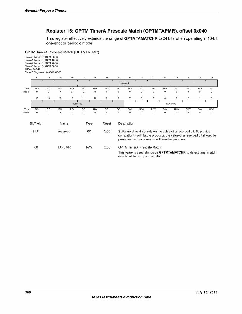
Register 15: GPTM TimerA Prescale Match (GPTMTAPMR), offset 0x040This register effectively extends the range of GPTMTAMATCHR to 24 bits when operating in 16-bitone-shot or periodic mode.
GPTM TimerA Prescale Match (GPTMTAPMR)Timer0 base: 0x4003.0000Timer1 base: 0x4003.1000Timer2 base: 0x4003.2000Timer3 base: 0x4003.3000Offset 0x040Type R/W, reset 0x0000.0000
16171819202122232425262728293031
reserved
ROROROROROROROROROROROROROROROROType0000000000000000Reset
0123456789101112131415
TAPSMRreserved
R/WR/WR/WR/WR/WR/WR/WR/WROROROROROROROROType0000000000000000Reset
DescriptionResetTypeNameBit/Field
Software should not rely on the value of a reserved bit. To providecompatibility with future products, the value of a reserved bit should bepreserved across a read-modify-write operation.
0x00ROreserved31:8
GPTM TimerA Prescale MatchThis value is used alongside GPTMTAMATCHR to detect timer matchevents while using a prescaler.
0x00R/WTAPSMR7:0
July 16, 2014360Texas Instruments-Production Data
General-Purpose Timers
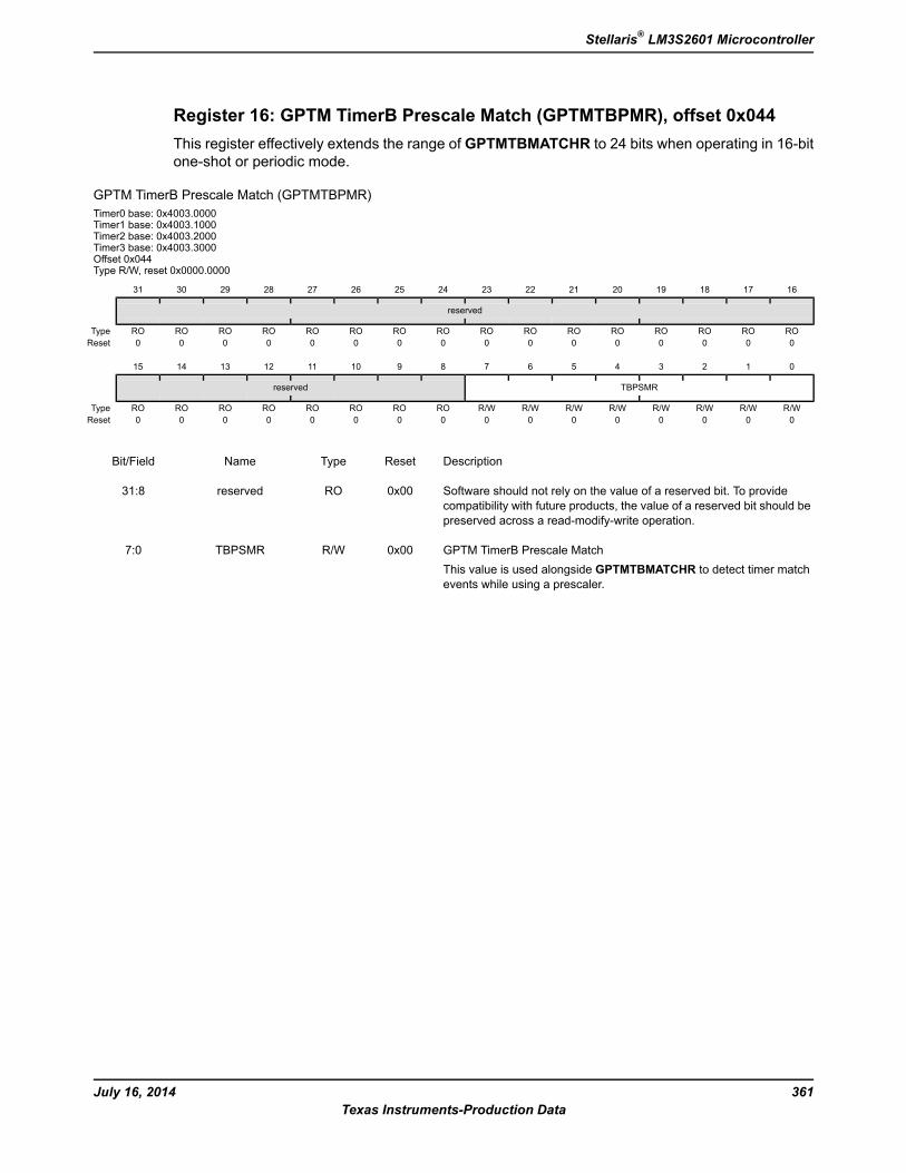
Register 16: GPTM TimerB Prescale Match (GPTMTBPMR), offset 0x044This register effectively extends the range of GPTMTBMATCHR to 24 bits when operating in 16-bitone-shot or periodic mode.
GPTM TimerB Prescale Match (GPTMTBPMR)Timer0 base: 0x4003.0000Timer1 base: 0x4003.1000Timer2 base: 0x4003.2000Timer3 base: 0x4003.3000Offset 0x044Type R/W, reset 0x0000.0000
16171819202122232425262728293031
reserved
ROROROROROROROROROROROROROROROROType0000000000000000Reset
0123456789101112131415
TBPSMRreserved
R/WR/WR/WR/WR/WR/WR/WR/WROROROROROROROROType0000000000000000Reset
DescriptionResetTypeNameBit/Field
Software should not rely on the value of a reserved bit. To providecompatibility with future products, the value of a reserved bit should bepreserved across a read-modify-write operation.
0x00ROreserved31:8
GPTM TimerB Prescale MatchThis value is used alongside GPTMTBMATCHR to detect timer matchevents while using a prescaler.
0x00R/WTBPSMR7:0
361July 16, 2014Texas Instruments-Production Data
Stellaris® LM3S2601 Microcontroller
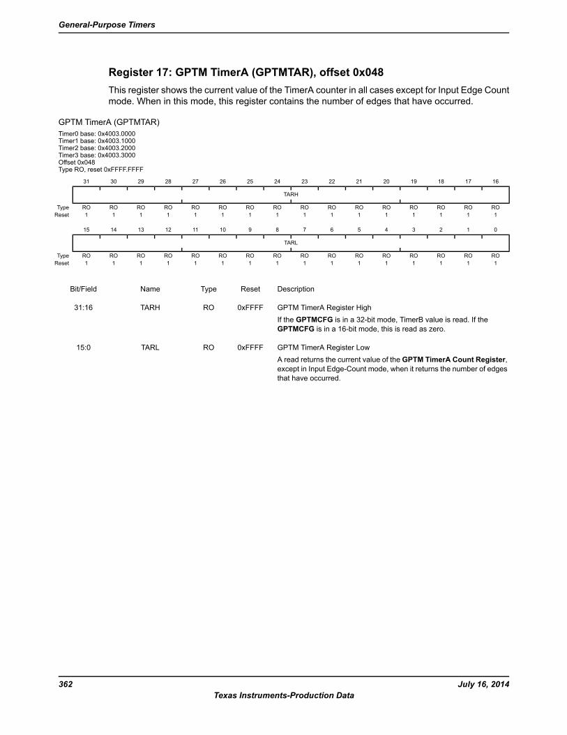
Register 17: GPTM TimerA (GPTMTAR), offset 0x048This register shows the current value of the TimerA counter in all cases except for Input Edge Countmode. When in this mode, this register contains the number of edges that have occurred.
GPTM TimerA (GPTMTAR)Timer0 base: 0x4003.0000Timer1 base: 0x4003.1000Timer2 base: 0x4003.2000Timer3 base: 0x4003.3000Offset 0x048Type RO, reset 0xFFFF.FFFF
16171819202122232425262728293031
TARH
ROROROROROROROROROROROROROROROROType1111111111111111Reset
0123456789101112131415
TARL
ROROROROROROROROROROROROROROROROType1111111111111111Reset
DescriptionResetTypeNameBit/Field
GPTM TimerA Register HighIf the GPTMCFG is in a 32-bit mode, TimerB value is read. If theGPTMCFG is in a 16-bit mode, this is read as zero.
0xFFFFROTARH31:16
GPTM TimerA Register LowA read returns the current value of the GPTM TimerA Count Register,except in Input Edge-Count mode, when it returns the number of edgesthat have occurred.
0xFFFFROTARL15:0
July 16, 2014362Texas Instruments-Production Data
General-Purpose Timers
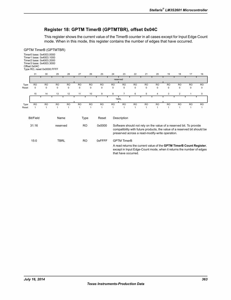
Register 18: GPTM TimerB (GPTMTBR), offset 0x04CThis register shows the current value of the TimerB counter in all cases except for Input Edge Countmode. When in this mode, this register contains the number of edges that have occurred.
GPTM TimerB (GPTMTBR)Timer0 base: 0x4003.0000Timer1 base: 0x4003.1000Timer2 base: 0x4003.2000Timer3 base: 0x4003.3000Offset 0x04CType RO, reset 0x0000.FFFF
16171819202122232425262728293031
reserved
ROROROROROROROROROROROROROROROROType0000000000000000Reset
0123456789101112131415
TBRL
ROROROROROROROROROROROROROROROROType1111111111111111Reset
DescriptionResetTypeNameBit/Field
Software should not rely on the value of a reserved bit. To providecompatibility with future products, the value of a reserved bit should bepreserved across a read-modify-write operation.
0x0000ROreserved31:16
GPTM TimerBA read returns the current value of the GPTM TimerB Count Register,except in Input Edge-Count mode, when it returns the number of edgesthat have occurred.
0xFFFFROTBRL15:0
363July 16, 2014Texas Instruments-Production Data
Stellaris® LM3S2601 Microcontroller
10 Watchdog TimerA watchdog timer can generate nonmaskable interrupts (NMIs) or a reset when a time-out value isreached. The watchdog timer is used to regain control when a system has failed due to a softwareerror or due to the failure of an external device to respond in the expected way.
The Stellaris® Watchdog Timer module has the following features:
32-bit down counter with a programmable load register
Separate watchdog clock with an enable
Programmable interrupt generation logic with interrupt masking
Lock register protection from runaway software
Reset generation logic with an enable/disable
User-enabled stalling when the controller asserts the CPU Halt flag during debug
TheWatchdog Timer can be configured to generate an interrupt to the controller on its first time-out,and to generate a reset signal on its second time-out. Once theWatchdog Timer has been configured,the lock register can be written to prevent the timer configuration from being inadvertently altered.
July 16, 2014364Texas Instruments-Production Data
Watchdog Timer
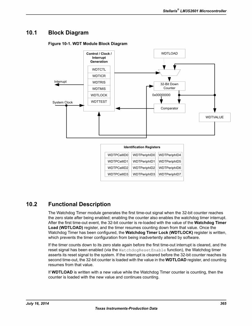
10.1 Block Diagram
Figure 10-1. WDT Module Block Diagram
Control / Clock /InterruptGeneration
WDTCTL
WDTICR
WDTRIS
WDTMIS
WDTLOCK
WDTTEST
WDTLOAD
WDTVALUE
Comparator
32-Bit DownCounter
0x00000000
Interrupt
System Clock
Identification Registers
WDTPCellID0 WDTPeriphID0 WDTPeriphID4
WDTPCellID1 WDTPeriphID1 WDTPeriphID5
WDTPCellID2 WDTPeriphID2 WDTPeriphID6
WDTPCellID3 WDTPeriphID3 WDTPeriphID7
10.2 Functional DescriptionThe Watchdog Timer module generates the first time-out signal when the 32-bit counter reachesthe zero state after being enabled; enabling the counter also enables the watchdog timer interrupt.After the first time-out event, the 32-bit counter is re-loaded with the value of theWatchdog TimerLoad (WDTLOAD) register, and the timer resumes counting down from that value. Once theWatchdog Timer has been configured, theWatchdog Timer Lock (WDTLOCK) register is written,which prevents the timer configuration from being inadvertently altered by software.
If the timer counts down to its zero state again before the first time-out interrupt is cleared, and thereset signal has been enabled (via the WatchdogResetEnable function), the Watchdog timerasserts its reset signal to the system. If the interrupt is cleared before the 32-bit counter reaches itssecond time-out, the 32-bit counter is loaded with the value in theWDTLOAD register, and countingresumes from that value.
IfWDTLOAD is written with a new value while the Watchdog Timer counter is counting, then thecounter is loaded with the new value and continues counting.
365July 16, 2014Texas Instruments-Production Data
Stellaris® LM3S2601 Microcontroller
Writing toWDTLOAD does not clear an active interrupt. An interrupt must be specifically clearedby writing to theWatchdog Interrupt Clear (WDTICR) register.
TheWatchdog module interrupt and reset generation can be enabled or disabled as required. Whenthe interrupt is re-enabled, the 32-bit counter is preloaded with the load register value and not itslast state.
10.3 Initialization and ConfigurationTo use the WDT, its peripheral clock must be enabled by setting the WDT bit in the RCGC0 register.The Watchdog Timer is configured using the following sequence:
1. Load theWDTLOAD register with the desired timer load value.
2. If theWatchdog is configured to trigger system resets, set the RESEN bit in theWDTCTL register.
3. Set the INTEN bit in theWDTCTL register to enable the Watchdog and lock the control register.
If software requires that all of the watchdog registers are locked, the Watchdog Timer module canbe fully locked by writing any value to theWDTLOCK register. To unlock the Watchdog Timer, writea value of 0x1ACC.E551.
10.4 Register MapTable 10-1 on page 366 lists the Watchdog registers. The offset listed is a hexadecimal incrementto the register’s address, relative to the Watchdog Timer base address of 0x4000.0000.
Table 10-1. Watchdog Timer Register Map
SeepageDescriptionResetTypeNameOffset
368Watchdog Load0xFFFF.FFFFR/WWDTLOAD0x000
369Watchdog Value0xFFFF.FFFFROWDTVALUE0x004
370Watchdog Control0x0000.0000R/WWDTCTL0x008
371Watchdog Interrupt Clear-WOWDTICR0x00C
372Watchdog Raw Interrupt Status0x0000.0000ROWDTRIS0x010
373Watchdog Masked Interrupt Status0x0000.0000ROWDTMIS0x014
374Watchdog Test0x0000.0000R/WWDTTEST0x418
375Watchdog Lock0x0000.0000R/WWDTLOCK0xC00
376Watchdog Peripheral Identification 40x0000.0000ROWDTPeriphID40xFD0
377Watchdog Peripheral Identification 50x0000.0000ROWDTPeriphID50xFD4
378Watchdog Peripheral Identification 60x0000.0000ROWDTPeriphID60xFD8
379Watchdog Peripheral Identification 70x0000.0000ROWDTPeriphID70xFDC
380Watchdog Peripheral Identification 00x0000.0005ROWDTPeriphID00xFE0
381Watchdog Peripheral Identification 10x0000.0018ROWDTPeriphID10xFE4
382Watchdog Peripheral Identification 20x0000.0018ROWDTPeriphID20xFE8
July 16, 2014366Texas Instruments-Production Data
Watchdog Timer
Table 10-1. Watchdog Timer Register Map (continued)
SeepageDescriptionResetTypeNameOffset
383Watchdog Peripheral Identification 30x0000.0001ROWDTPeriphID30xFEC
384Watchdog PrimeCell Identification 00x0000.000DROWDTPCellID00xFF0
385Watchdog PrimeCell Identification 10x0000.00F0ROWDTPCellID10xFF4
386Watchdog PrimeCell Identification 20x0000.0005ROWDTPCellID20xFF8
387Watchdog PrimeCell Identification 30x0000.00B1ROWDTPCellID30xFFC
10.5 Register DescriptionsThe remainder of this section lists and describes the WDT registers, in numerical order by addressoffset.
367July 16, 2014Texas Instruments-Production Data
Stellaris® LM3S2601 Microcontroller
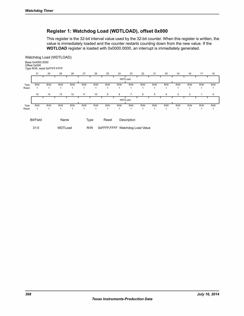
Register 1: Watchdog Load (WDTLOAD), offset 0x000This register is the 32-bit interval value used by the 32-bit counter. When this register is written, thevalue is immediately loaded and the counter restarts counting down from the new value. If theWDTLOAD register is loaded with 0x0000.0000, an interrupt is immediately generated.
Watchdog Load (WDTLOAD)Base 0x4000.0000Offset 0x000Type R/W, reset 0xFFFF.FFFF
16171819202122232425262728293031
WDTLoad
R/WR/WR/WR/WR/WR/WR/WR/WR/WR/WR/WR/WR/WR/WR/WR/WType1111111111111111Reset
0123456789101112131415
WDTLoad
R/WR/WR/WR/WR/WR/WR/WR/WR/WR/WR/WR/WR/WR/WR/WR/WType1111111111111111Reset
DescriptionResetTypeNameBit/Field
Watchdog Load Value0xFFFF.FFFFR/WWDTLoad31:0
July 16, 2014368Texas Instruments-Production Data
Watchdog Timer
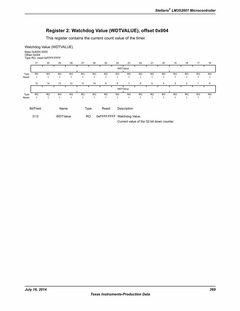
Register 2: Watchdog Value (WDTVALUE), offset 0x004This register contains the current count value of the timer.
Watchdog Value (WDTVALUE)Base 0x4000.0000Offset 0x004Type RO, reset 0xFFFF.FFFF
16171819202122232425262728293031
WDTValue
ROROROROROROROROROROROROROROROROType1111111111111111Reset
0123456789101112131415
WDTValue
ROROROROROROROROROROROROROROROROType1111111111111111Reset
DescriptionResetTypeNameBit/Field
Watchdog ValueCurrent value of the 32-bit down counter.
0xFFFF.FFFFROWDTValue31:0
369July 16, 2014Texas Instruments-Production Data
Stellaris® LM3S2601 Microcontroller
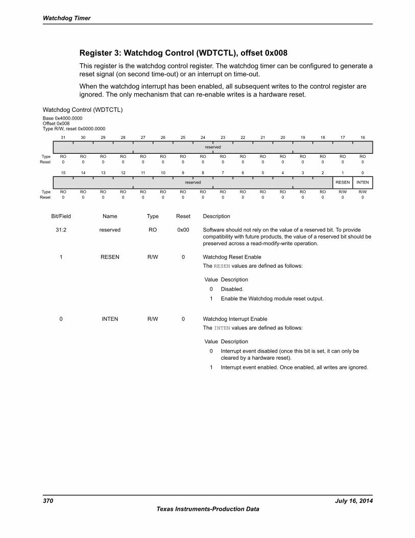
Register 3: Watchdog Control (WDTCTL), offset 0x008This register is the watchdog control register. The watchdog timer can be configured to generate areset signal (on second time-out) or an interrupt on time-out.
When the watchdog interrupt has been enabled, all subsequent writes to the control register areignored. The only mechanism that can re-enable writes is a hardware reset.
Watchdog Control (WDTCTL)Base 0x4000.0000Offset 0x008Type R/W, reset 0x0000.0000
16171819202122232425262728293031
reserved
ROROROROROROROROROROROROROROROROType0000000000000000Reset
0123456789101112131415
INTENRESENreserved
R/WR/WROROROROROROROROROROROROROROType0000000000000000Reset
DescriptionResetTypeNameBit/Field
Software should not rely on the value of a reserved bit. To providecompatibility with future products, the value of a reserved bit should bepreserved across a read-modify-write operation.
0x00ROreserved31:2
Watchdog Reset EnableThe RESEN values are defined as follows:
DescriptionValue
Disabled.0
Enable the Watchdog module reset output.1
0R/WRESEN1
Watchdog Interrupt EnableThe INTEN values are defined as follows:
DescriptionValue
Interrupt event disabled (once this bit is set, it can only becleared by a hardware reset).
0
Interrupt event enabled. Once enabled, all writes are ignored.1
0R/WINTEN0
July 16, 2014370Texas Instruments-Production Data
Watchdog Timer
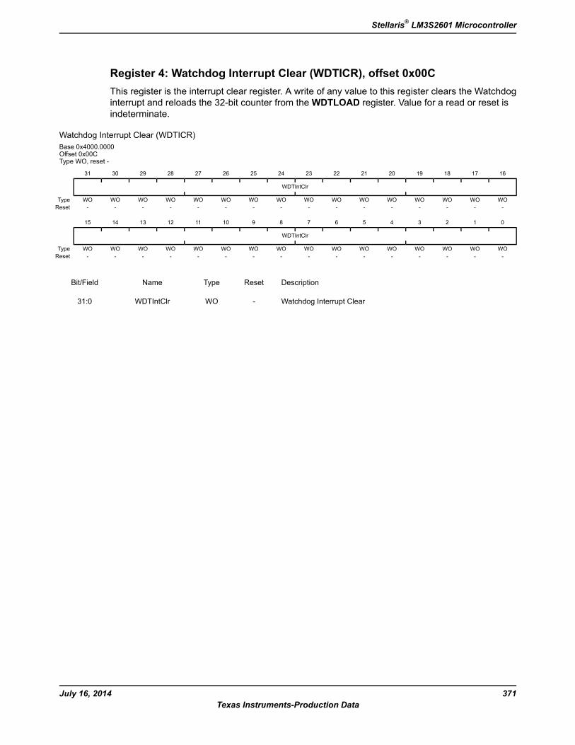
Register 4: Watchdog Interrupt Clear (WDTICR), offset 0x00CThis register is the interrupt clear register. A write of any value to this register clears the Watchdoginterrupt and reloads the 32-bit counter from theWDTLOAD register. Value for a read or reset isindeterminate.
Watchdog Interrupt Clear (WDTICR)Base 0x4000.0000Offset 0x00CType WO, reset -
16171819202122232425262728293031
WDTIntClr
WOWOWOWOWOWOWOWOWOWOWOWOWOWOWOWOType----------------Reset
0123456789101112131415
WDTIntClr
WOWOWOWOWOWOWOWOWOWOWOWOWOWOWOWOType----------------Reset
DescriptionResetTypeNameBit/Field
Watchdog Interrupt Clear-WOWDTIntClr31:0
371July 16, 2014Texas Instruments-Production Data
Stellaris® LM3S2601 Microcontroller
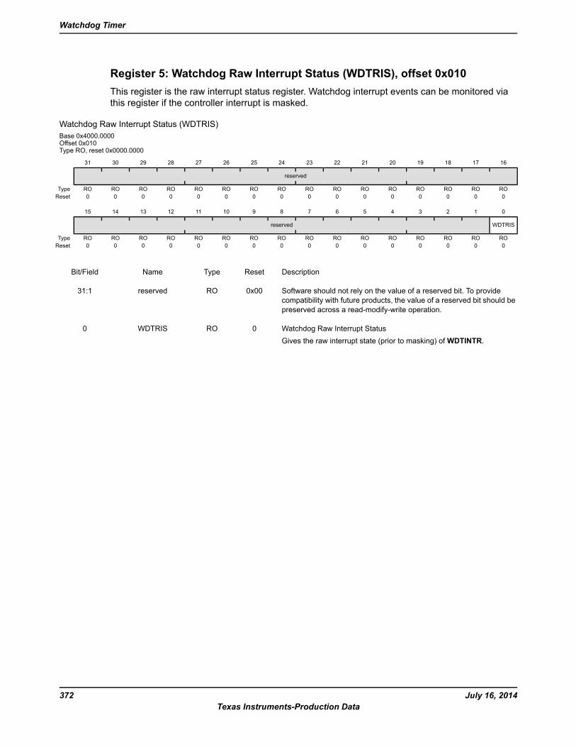
Register 5: Watchdog Raw Interrupt Status (WDTRIS), offset 0x010This register is the raw interrupt status register. Watchdog interrupt events can be monitored viathis register if the controller interrupt is masked.
Watchdog Raw Interrupt Status (WDTRIS)Base 0x4000.0000Offset 0x010Type RO, reset 0x0000.0000
16171819202122232425262728293031
reserved
ROROROROROROROROROROROROROROROROType0000000000000000Reset
0123456789101112131415
WDTRISreserved
ROROROROROROROROROROROROROROROROType0000000000000000Reset
DescriptionResetTypeNameBit/Field
Software should not rely on the value of a reserved bit. To providecompatibility with future products, the value of a reserved bit should bepreserved across a read-modify-write operation.
0x00ROreserved31:1
Watchdog Raw Interrupt StatusGives the raw interrupt state (prior to masking) ofWDTINTR.
0ROWDTRIS0
July 16, 2014372Texas Instruments-Production Data
Watchdog Timer
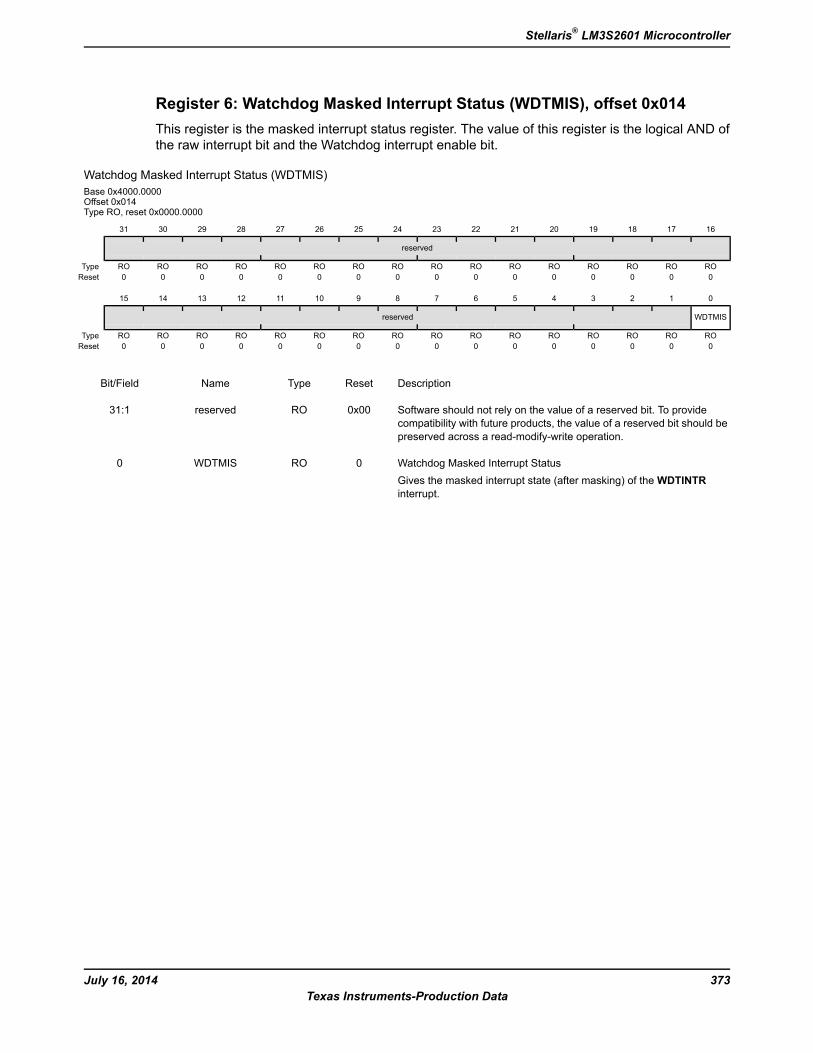
Register 6: Watchdog Masked Interrupt Status (WDTMIS), offset 0x014This register is the masked interrupt status register. The value of this register is the logical AND ofthe raw interrupt bit and the Watchdog interrupt enable bit.
Watchdog Masked Interrupt Status (WDTMIS)Base 0x4000.0000Offset 0x014Type RO, reset 0x0000.0000
16171819202122232425262728293031
reserved
ROROROROROROROROROROROROROROROROType0000000000000000Reset
0123456789101112131415
WDTMISreserved
ROROROROROROROROROROROROROROROROType0000000000000000Reset
DescriptionResetTypeNameBit/Field
Software should not rely on the value of a reserved bit. To providecompatibility with future products, the value of a reserved bit should bepreserved across a read-modify-write operation.
0x00ROreserved31:1
Watchdog Masked Interrupt StatusGives the masked interrupt state (after masking) of theWDTINTRinterrupt.
0ROWDTMIS0
373July 16, 2014Texas Instruments-Production Data
Stellaris® LM3S2601 Microcontroller
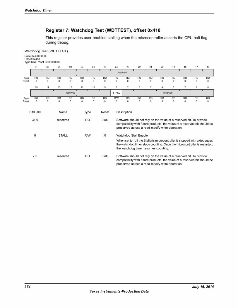
Register 7: Watchdog Test (WDTTEST), offset 0x418This register provides user-enabled stalling when the microcontroller asserts the CPU halt flagduring debug.
Watchdog Test (WDTTEST)Base 0x4000.0000Offset 0x418Type R/W, reset 0x0000.0000
16171819202122232425262728293031
reserved
ROROROROROROROROROROROROROROROROType0000000000000000Reset
0123456789101112131415
reservedSTALLreserved
ROROROROROROROROR/WROROROROROROROType0000000000000000Reset
DescriptionResetTypeNameBit/Field
Software should not rely on the value of a reserved bit. To providecompatibility with future products, the value of a reserved bit should bepreserved across a read-modify-write operation.
0x00ROreserved31:9
Watchdog Stall EnableWhen set to 1, if the Stellaris microcontroller is stopped with a debugger,the watchdog timer stops counting. Once the microcontroller is restarted,the watchdog timer resumes counting.
0R/WSTALL8
Software should not rely on the value of a reserved bit. To providecompatibility with future products, the value of a reserved bit should bepreserved across a read-modify-write operation.
0x00ROreserved7:0
July 16, 2014374Texas Instruments-Production Data
Watchdog Timer
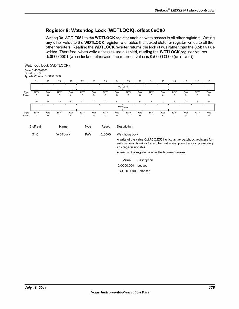
Register 8: Watchdog Lock (WDTLOCK), offset 0xC00Writing 0x1ACC.E551 to theWDTLOCK register enables write access to all other registers. Writingany other value to theWDTLOCK register re-enables the locked state for register writes to all theother registers. Reading theWDTLOCK register returns the lock status rather than the 32-bit valuewritten. Therefore, when write accesses are disabled, reading theWDTLOCK register returns0x0000.0001 (when locked; otherwise, the returned value is 0x0000.0000 (unlocked)).
Watchdog Lock (WDTLOCK)Base 0x4000.0000Offset 0xC00Type R/W, reset 0x0000.0000
16171819202122232425262728293031
WDTLock
R/WR/WR/WR/WR/WR/WR/WR/WR/WR/WR/WR/WR/WR/WR/WR/WType0000000000000000Reset
0123456789101112131415
WDTLock
R/WR/WR/WR/WR/WR/WR/WR/WR/WR/WR/WR/WR/WR/WR/WR/WType0000000000000000Reset
DescriptionResetTypeNameBit/Field
Watchdog LockA write of the value 0x1ACC.E551 unlocks the watchdog registers forwrite access. A write of any other value reapplies the lock, preventingany register updates.A read of this register returns the following values:
DescriptionValue
Locked0x0000.0001
Unlocked0x0000.0000
0x0000R/WWDTLock31:0
375July 16, 2014Texas Instruments-Production Data
Stellaris® LM3S2601 Microcontroller

Register 9:Watchdog Peripheral Identification 4 (WDTPeriphID4), offset 0xFD0TheWDTPeriphIDn registers are hard-coded and the fields within the register determine the resetvalue.
Watchdog Peripheral Identification 4 (WDTPeriphID4)Base 0x4000.0000Offset 0xFD0Type RO, reset 0x0000.0000
16171819202122232425262728293031
reserved
ROROROROROROROROROROROROROROROROType0000000000000000Reset
0123456789101112131415
PID4reserved
ROROROROROROROROROROROROROROROROType0000000000000000Reset
DescriptionResetTypeNameBit/Field
Software should not rely on the value of a reserved bit. To providecompatibility with future products, the value of a reserved bit should bepreserved across a read-modify-write operation.
0x00ROreserved31:8
WDT Peripheral ID Register[7:0]0x00ROPID47:0
July 16, 2014376Texas Instruments-Production Data
Watchdog Timer
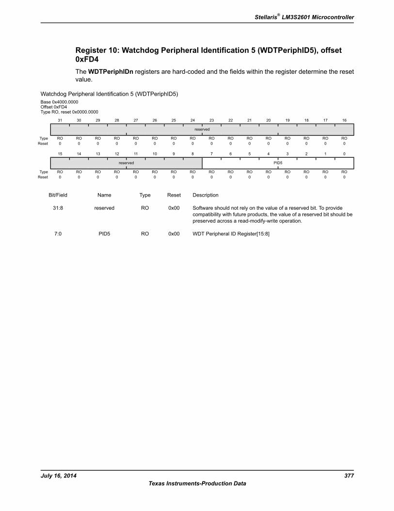
Register 10: Watchdog Peripheral Identification 5 (WDTPeriphID5), offset0xFD4TheWDTPeriphIDn registers are hard-coded and the fields within the register determine the resetvalue.
Watchdog Peripheral Identification 5 (WDTPeriphID5)Base 0x4000.0000Offset 0xFD4Type RO, reset 0x0000.0000
16171819202122232425262728293031
reserved
ROROROROROROROROROROROROROROROROType0000000000000000Reset
0123456789101112131415
PID5reserved
ROROROROROROROROROROROROROROROROType0000000000000000Reset
DescriptionResetTypeNameBit/Field
Software should not rely on the value of a reserved bit. To providecompatibility with future products, the value of a reserved bit should bepreserved across a read-modify-write operation.
0x00ROreserved31:8
WDT Peripheral ID Register[15:8]0x00ROPID57:0
377July 16, 2014Texas Instruments-Production Data
Stellaris® LM3S2601 Microcontroller
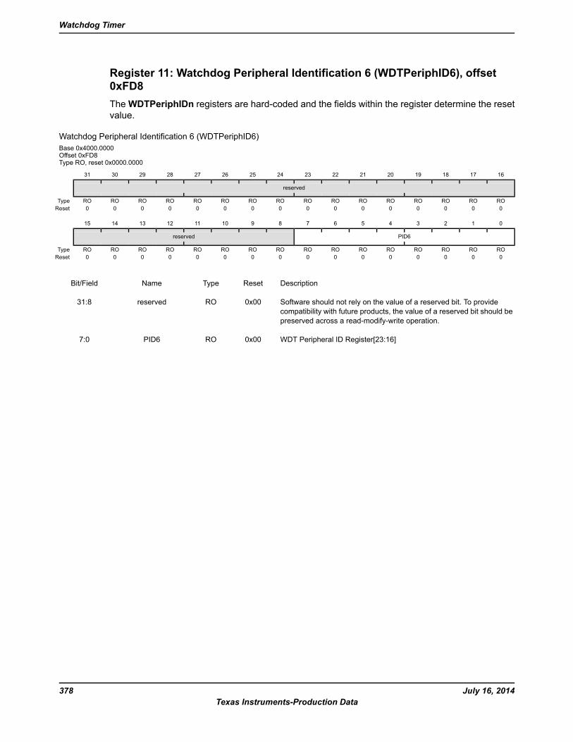
Register 11: Watchdog Peripheral Identification 6 (WDTPeriphID6), offset0xFD8TheWDTPeriphIDn registers are hard-coded and the fields within the register determine the resetvalue.
Watchdog Peripheral Identification 6 (WDTPeriphID6)Base 0x4000.0000Offset 0xFD8Type RO, reset 0x0000.0000
16171819202122232425262728293031
reserved
ROROROROROROROROROROROROROROROROType0000000000000000Reset
0123456789101112131415
PID6reserved
ROROROROROROROROROROROROROROROROType0000000000000000Reset
DescriptionResetTypeNameBit/Field
Software should not rely on the value of a reserved bit. To providecompatibility with future products, the value of a reserved bit should bepreserved across a read-modify-write operation.
0x00ROreserved31:8
WDT Peripheral ID Register[23:16]0x00ROPID67:0
July 16, 2014378Texas Instruments-Production Data
Watchdog Timer

Register 12: Watchdog Peripheral Identification 7 (WDTPeriphID7), offset0xFDCTheWDTPeriphIDn registers are hard-coded and the fields within the register determine the resetvalue.
Watchdog Peripheral Identification 7 (WDTPeriphID7)Base 0x4000.0000Offset 0xFDCType RO, reset 0x0000.0000
16171819202122232425262728293031
reserved
ROROROROROROROROROROROROROROROROType0000000000000000Reset
0123456789101112131415
PID7reserved
ROROROROROROROROROROROROROROROROType0000000000000000Reset
DescriptionResetTypeNameBit/Field
Software should not rely on the value of a reserved bit. To providecompatibility with future products, the value of a reserved bit should bepreserved across a read-modify-write operation.
0x00ROreserved31:8
WDT Peripheral ID Register[31:24]0x00ROPID77:0
379July 16, 2014Texas Instruments-Production Data
Stellaris® LM3S2601 Microcontroller
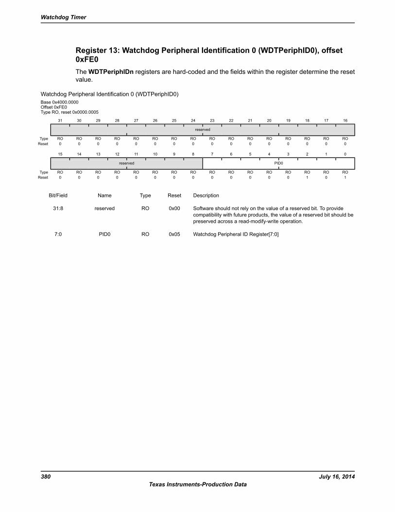
Register 13: Watchdog Peripheral Identification 0 (WDTPeriphID0), offset0xFE0TheWDTPeriphIDn registers are hard-coded and the fields within the register determine the resetvalue.
Watchdog Peripheral Identification 0 (WDTPeriphID0)Base 0x4000.0000Offset 0xFE0Type RO, reset 0x0000.0005
16171819202122232425262728293031
reserved
ROROROROROROROROROROROROROROROROType0000000000000000Reset
0123456789101112131415
PID0reserved
ROROROROROROROROROROROROROROROROType1010000000000000Reset
DescriptionResetTypeNameBit/Field
Software should not rely on the value of a reserved bit. To providecompatibility with future products, the value of a reserved bit should bepreserved across a read-modify-write operation.
0x00ROreserved31:8
Watchdog Peripheral ID Register[7:0]0x05ROPID07:0
July 16, 2014380Texas Instruments-Production Data
Watchdog Timer

Register 14: Watchdog Peripheral Identification 1 (WDTPeriphID1), offset0xFE4TheWDTPeriphIDn registers are hard-coded and the fields within the register determine the resetvalue.
Watchdog Peripheral Identification 1 (WDTPeriphID1)Base 0x4000.0000Offset 0xFE4Type RO, reset 0x0000.0018
16171819202122232425262728293031
reserved
ROROROROROROROROROROROROROROROROType0000000000000000Reset
0123456789101112131415
PID1reserved
ROROROROROROROROROROROROROROROROType0001100000000000Reset
DescriptionResetTypeNameBit/Field
Software should not rely on the value of a reserved bit. To providecompatibility with future products, the value of a reserved bit should bepreserved across a read-modify-write operation.
0x00ROreserved31:8
Watchdog Peripheral ID Register[15:8]0x18ROPID17:0
381July 16, 2014Texas Instruments-Production Data
Stellaris® LM3S2601 Microcontroller

Register 15: Watchdog Peripheral Identification 2 (WDTPeriphID2), offset0xFE8TheWDTPeriphIDn registers are hard-coded and the fields within the register determine the resetvalue.
Watchdog Peripheral Identification 2 (WDTPeriphID2)Base 0x4000.0000Offset 0xFE8Type RO, reset 0x0000.0018
16171819202122232425262728293031
reserved
ROROROROROROROROROROROROROROROROType0000000000000000Reset
0123456789101112131415
PID2reserved
ROROROROROROROROROROROROROROROROType0001100000000000Reset
DescriptionResetTypeNameBit/Field
Software should not rely on the value of a reserved bit. To providecompatibility with future products, the value of a reserved bit should bepreserved across a read-modify-write operation.
0x00ROreserved31:8
Watchdog Peripheral ID Register[23:16]0x18ROPID27:0
July 16, 2014382Texas Instruments-Production Data
Watchdog Timer
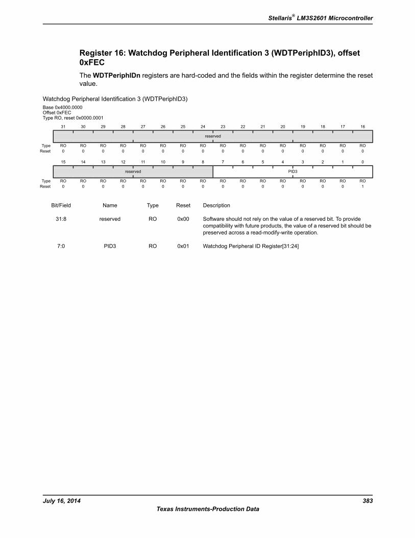
Register 16: Watchdog Peripheral Identification 3 (WDTPeriphID3), offset0xFECTheWDTPeriphIDn registers are hard-coded and the fields within the register determine the resetvalue.
Watchdog Peripheral Identification 3 (WDTPeriphID3)Base 0x4000.0000Offset 0xFECType RO, reset 0x0000.0001
16171819202122232425262728293031
reserved
ROROROROROROROROROROROROROROROROType0000000000000000Reset
0123456789101112131415
PID3reserved
ROROROROROROROROROROROROROROROROType1000000000000000Reset
DescriptionResetTypeNameBit/Field
Software should not rely on the value of a reserved bit. To providecompatibility with future products, the value of a reserved bit should bepreserved across a read-modify-write operation.
0x00ROreserved31:8
Watchdog Peripheral ID Register[31:24]0x01ROPID37:0
383July 16, 2014Texas Instruments-Production Data
Stellaris® LM3S2601 Microcontroller

Register 17: Watchdog PrimeCell Identification 0 (WDTPCellID0), offset 0xFF0TheWDTPCellIDn registers are hard-coded and the fields within the register determine the resetvalue.
Watchdog PrimeCell Identification 0 (WDTPCellID0)Base 0x4000.0000Offset 0xFF0Type RO, reset 0x0000.000D
16171819202122232425262728293031
reserved
ROROROROROROROROROROROROROROROROType0000000000000000Reset
0123456789101112131415
CID0reserved
ROROROROROROROROROROROROROROROROType1011000000000000Reset
DescriptionResetTypeNameBit/Field
Software should not rely on the value of a reserved bit. To providecompatibility with future products, the value of a reserved bit should bepreserved across a read-modify-write operation.
0x00ROreserved31:8
Watchdog PrimeCell ID Register[7:0]0x0DROCID07:0
July 16, 2014384Texas Instruments-Production Data
Watchdog Timer
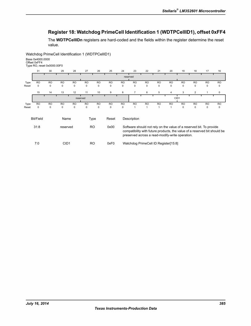
Register 18: Watchdog PrimeCell Identification 1 (WDTPCellID1), offset 0xFF4TheWDTPCellIDn registers are hard-coded and the fields within the register determine the resetvalue.
Watchdog PrimeCell Identification 1 (WDTPCellID1)Base 0x4000.0000Offset 0xFF4Type RO, reset 0x0000.00F0
16171819202122232425262728293031
reserved
ROROROROROROROROROROROROROROROROType0000000000000000Reset
0123456789101112131415
CID1reserved
ROROROROROROROROROROROROROROROROType0000111100000000Reset
DescriptionResetTypeNameBit/Field
Software should not rely on the value of a reserved bit. To providecompatibility with future products, the value of a reserved bit should bepreserved across a read-modify-write operation.
0x00ROreserved31:8
Watchdog PrimeCell ID Register[15:8]0xF0ROCID17:0
385July 16, 2014Texas Instruments-Production Data
Stellaris® LM3S2601 Microcontroller
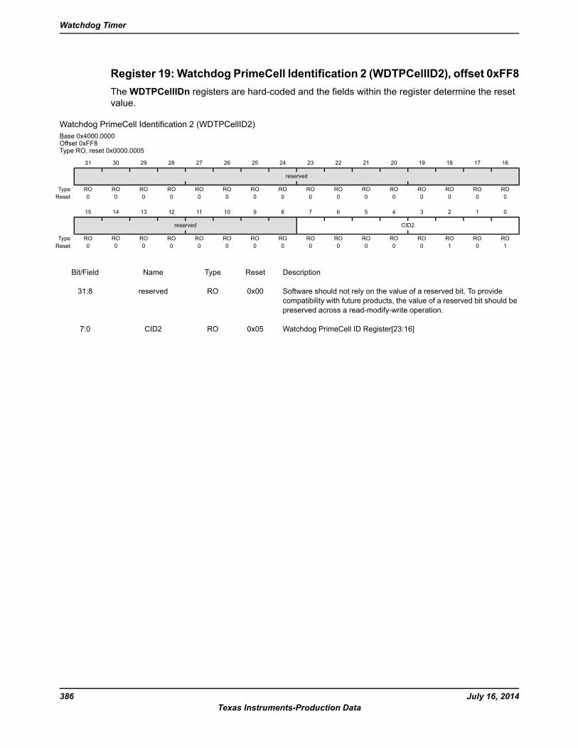
Register 19: Watchdog PrimeCell Identification 2 (WDTPCellID2), offset 0xFF8TheWDTPCellIDn registers are hard-coded and the fields within the register determine the resetvalue.
Watchdog PrimeCell Identification 2 (WDTPCellID2)Base 0x4000.0000Offset 0xFF8Type RO, reset 0x0000.0005
16171819202122232425262728293031
reserved
ROROROROROROROROROROROROROROROROType0000000000000000Reset
0123456789101112131415
CID2reserved
ROROROROROROROROROROROROROROROROType1010000000000000Reset
DescriptionResetTypeNameBit/Field
Software should not rely on the value of a reserved bit. To providecompatibility with future products, the value of a reserved bit should bepreserved across a read-modify-write operation.
0x00ROreserved31:8
Watchdog PrimeCell ID Register[23:16]0x05ROCID27:0
July 16, 2014386Texas Instruments-Production Data
Watchdog Timer

Register 20:Watchdog PrimeCell Identification 3 (WDTPCellID3 ), offset 0xFFCTheWDTPCellIDn registers are hard-coded and the fields within the register determine the resetvalue.
Watchdog PrimeCell Identification 3 (WDTPCellID3)Base 0x4000.0000Offset 0xFFCType RO, reset 0x0000.00B1
16171819202122232425262728293031
reserved
ROROROROROROROROROROROROROROROROType0000000000000000Reset
0123456789101112131415
CID3reserved
ROROROROROROROROROROROROROROROROType1000110100000000Reset
DescriptionResetTypeNameBit/Field
Software should not rely on the value of a reserved bit. To providecompatibility with future products, the value of a reserved bit should bepreserved across a read-modify-write operation.
0x00ROreserved31:8
Watchdog PrimeCell ID Register[31:24]0xB1ROCID37:0
387July 16, 2014Texas Instruments-Production Data
Stellaris® LM3S2601 Microcontroller
11 Universal Asynchronous Receivers/Transmitters(UARTs)Each Stellaris® Universal Asynchronous Receiver/Transmitter (UART) has the following features:
Three fully programmable 16C550-type UARTs with IrDA support
Separate 16x8 transmit (TX) and receive (RX) FIFOs to reduce CPU interrupt service loading
Programmable baud-rate generator allowing speeds up to 3.125 Mbps
Programmable FIFO length, including 1-byte deep operation providing conventionaldouble-buffered interface
FIFO trigger levels of 1/8, 1/4, 1/2, 3/4, and 7/8
Standard asynchronous communication bits for start, stop, and parity
Line-break generation and detection
Fully programmable serial interface characteristics
– 5, 6, 7, or 8 data bits
– Even, odd, stick, or no-parity bit generation/detection
– 1 or 2 stop bit generation
IrDA serial-IR (SIR) encoder/decoder providing
– Programmable use of IrDA Serial Infrared (SIR) or UART input/output
– Support of IrDA SIR encoder/decoder functions for data rates up to 115.2 Kbps half-duplex
– Support of normal 3/16 and low-power (1.41-2.23 μs) bit durations
– Programmable internal clock generator enabling division of reference clock by 1 to 256 forlow-power mode bit duration
July 16, 2014388Texas Instruments-Production Data
Universal Asynchronous Receivers/Transmitters (UARTs)
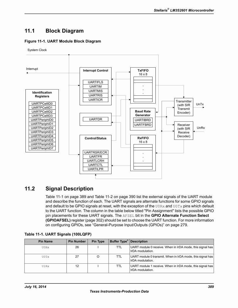
11.1 Block Diagram
Figure 11-1. UART Module Block Diagram
TxFIFO16 x 8
.
.
.
RxFIFO16 x 8
.
.
.
IdentificationRegisters
UARTPCellID0UARTPCellID1UARTPCellID2UARTPCellID3UARTPeriphID0UARTPeriphID1UARTPeriphID2UARTPeriphID3UARTPeriphID4UARTPeriphID5UARTPeriphID6UARTPeriphID7
Interrupt Control
UARTDR
Control/Status
Transmitter(with SIRTransmitEncoder)Baud Rate
Generator
Receiver(with SIRReceiveDecoder)
UnTx
UnRx
System Clock
Interrupt
UARTIFLSUARTIMUARTMISUARTRISUARTICR
UARTIBRDUARTFBRD
UARTRSR/ECRUARTFR
UARTLCRHUARTCTLUARTILPR
11.2 Signal DescriptionTable 11-1 on page 389 and Table 11-2 on page 390 list the external signals of the UART moduleand describe the function of each. The UART signals are alternate functions for some GPIO signalsand default to be GPIO signals at reset, with the exception of the U0Rx and U0Tx pins which defaultto the UART function. The column in the table below titled "Pin Assignment" lists the possible GPIOpin placements for these UART signals. The AFSEL bit in the GPIO Alternate Function Select(GPIOAFSEL) register (page 302) should be set to choose the UART function. For more informationon configuring GPIOs, see “General-Purpose Input/Outputs (GPIOs)” on page 279.
Table 11-1. UART Signals (100LQFP)
DescriptionBuffer TypeaPin TypePin NumberPin Name
UART module 0 receive. When in IrDA mode, this signal hasIrDA modulation.
TTLI26U0Rx
UARTmodule 0 transmit. When in IrDA mode, this signal hasIrDA modulation.
TTLO27U0Tx
UART module 1 receive. When in IrDA mode, this signal hasIrDA modulation.
TTLI12U1Rx
389July 16, 2014Texas Instruments-Production Data
Stellaris® LM3S2601 Microcontroller
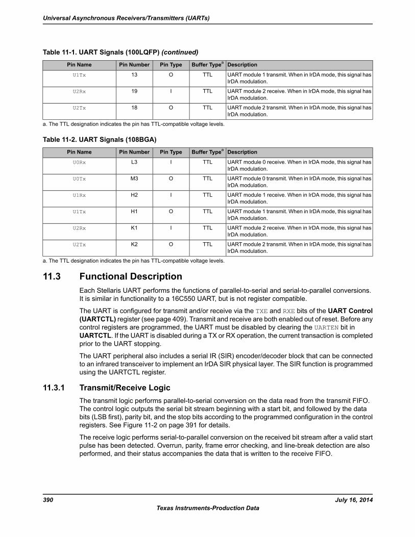
Table 11-1. UART Signals (100LQFP) (continued)
DescriptionBuffer TypeaPin TypePin NumberPin Name
UARTmodule 1 transmit. When in IrDA mode, this signal hasIrDA modulation.
TTLO13U1Tx
UART module 2 receive. When in IrDA mode, this signal hasIrDA modulation.
TTLI19U2Rx
UARTmodule 2 transmit. When in IrDA mode, this signal hasIrDA modulation.
TTLO18U2Tx
a. The TTL designation indicates the pin has TTL-compatible voltage levels.
Table 11-2. UART Signals (108BGA)
DescriptionBuffer TypeaPin TypePin NumberPin Name
UART module 0 receive. When in IrDA mode, this signal hasIrDA modulation.
TTLIL3U0Rx
UARTmodule 0 transmit. When in IrDA mode, this signal hasIrDA modulation.
TTLOM3U0Tx
UART module 1 receive. When in IrDA mode, this signal hasIrDA modulation.
TTLIH2U1Rx
UARTmodule 1 transmit. When in IrDA mode, this signal hasIrDA modulation.
TTLOH1U1Tx
UART module 2 receive. When in IrDA mode, this signal hasIrDA modulation.
TTLIK1U2Rx
UARTmodule 2 transmit. When in IrDA mode, this signal hasIrDA modulation.
TTLOK2U2Tx
a. The TTL designation indicates the pin has TTL-compatible voltage levels.
11.3 Functional DescriptionEach Stellaris UART performs the functions of parallel-to-serial and serial-to-parallel conversions.It is similar in functionality to a 16C550 UART, but is not register compatible.
The UART is configured for transmit and/or receive via the TXE and RXE bits of the UART Control(UARTCTL) register (see page 409). Transmit and receive are both enabled out of reset. Before anycontrol registers are programmed, the UART must be disabled by clearing the UARTEN bit inUARTCTL. If the UART is disabled during a TX or RX operation, the current transaction is completedprior to the UART stopping.
The UART peripheral also includes a serial IR (SIR) encoder/decoder block that can be connectedto an infrared transceiver to implement an IrDA SIR physical layer. The SIR function is programmedusing the UARTCTL register.
11.3.1 Transmit/Receive LogicThe transmit logic performs parallel-to-serial conversion on the data read from the transmit FIFO.The control logic outputs the serial bit stream beginning with a start bit, and followed by the databits (LSB first), parity bit, and the stop bits according to the programmed configuration in the controlregisters. See Figure 11-2 on page 391 for details.
The receive logic performs serial-to-parallel conversion on the received bit stream after a valid startpulse has been detected. Overrun, parity, frame error checking, and line-break detection are alsoperformed, and their status accompanies the data that is written to the receive FIFO.
July 16, 2014390Texas Instruments-Production Data
Universal Asynchronous Receivers/Transmitters (UARTs)
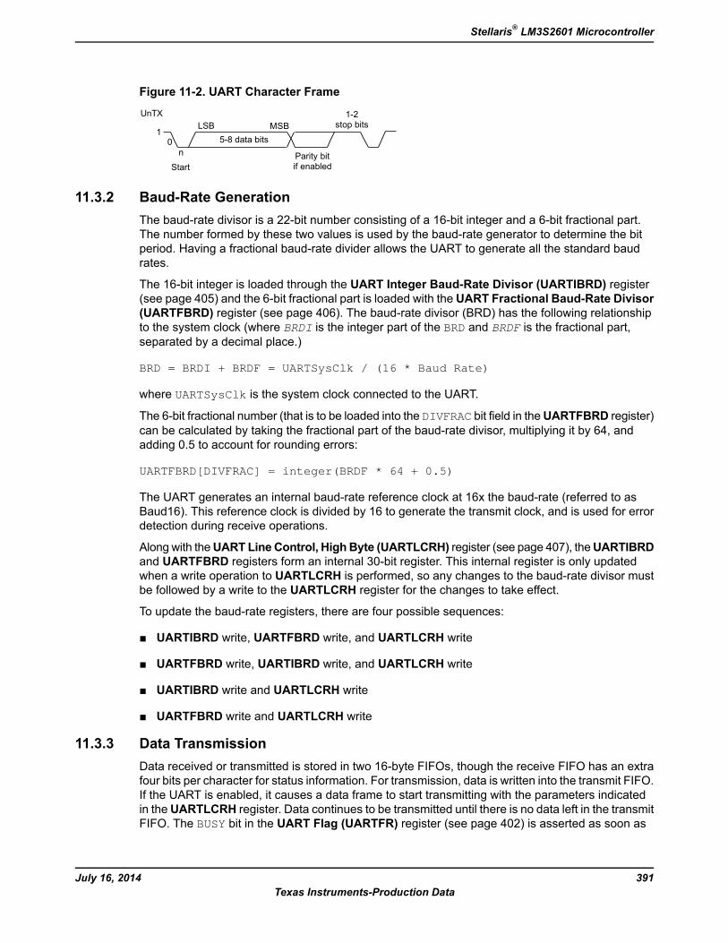
Figure 11-2. UART Character Frame
10 5-8 data bits
LSB MSB
Parity bitif enabled
1-2stop bits
UnTX
n
Start
11.3.2 Baud-Rate GenerationThe baud-rate divisor is a 22-bit number consisting of a 16-bit integer and a 6-bit fractional part.The number formed by these two values is used by the baud-rate generator to determine the bitperiod. Having a fractional baud-rate divider allows the UART to generate all the standard baudrates.
The 16-bit integer is loaded through the UART Integer Baud-Rate Divisor (UARTIBRD) register(see page 405) and the 6-bit fractional part is loaded with the UART Fractional Baud-Rate Divisor(UARTFBRD) register (see page 406). The baud-rate divisor (BRD) has the following relationshipto the system clock (where BRDI is the integer part of the BRD and BRDF is the fractional part,separated by a decimal place.)
BRD = BRDI + BRDF = UARTSysClk / (16 * Baud Rate)
where UARTSysClk is the system clock connected to the UART.
The 6-bit fractional number (that is to be loaded into the DIVFRAC bit field in theUARTFBRD register)can be calculated by taking the fractional part of the baud-rate divisor, multiplying it by 64, andadding 0.5 to account for rounding errors:
UARTFBRD[DIVFRAC] = integer(BRDF * 64 + 0.5)
The UART generates an internal baud-rate reference clock at 16x the baud-rate (referred to asBaud16). This reference clock is divided by 16 to generate the transmit clock, and is used for errordetection during receive operations.
Along with theUARTLineControl, HighByte (UARTLCRH) register (see page 407), theUARTIBRDand UARTFBRD registers form an internal 30-bit register. This internal register is only updatedwhen a write operation to UARTLCRH is performed, so any changes to the baud-rate divisor mustbe followed by a write to the UARTLCRH register for the changes to take effect.
To update the baud-rate registers, there are four possible sequences:
UARTIBRD write, UARTFBRD write, and UARTLCRH write
UARTFBRD write, UARTIBRD write, and UARTLCRH write
UARTIBRD write and UARTLCRH write
UARTFBRD write and UARTLCRH write
11.3.3 Data TransmissionData received or transmitted is stored in two 16-byte FIFOs, though the receive FIFO has an extrafour bits per character for status information. For transmission, data is written into the transmit FIFO.If the UART is enabled, it causes a data frame to start transmitting with the parameters indicatedin theUARTLCRH register. Data continues to be transmitted until there is no data left in the transmitFIFO. The BUSY bit in the UART Flag (UARTFR) register (see page 402) is asserted as soon as
391July 16, 2014Texas Instruments-Production Data
Stellaris® LM3S2601 Microcontroller
data is written to the transmit FIFO (that is, if the FIFO is non-empty) and remains asserted whiledata is being transmitted. The BUSY bit is negated only when the transmit FIFO is empty, and thelast character has been transmitted from the shift register, including the stop bits. The UART canindicate that it is busy even though the UART may no longer be enabled.
When the receiver is idle (the UnRx is continuously 1) and the data input goes Low (a start bit hasbeen received), the receive counter begins running and data is sampled on the eighth cycle ofBaud16 (described in “Transmit/Receive Logic” on page 390).
The start bit is valid and recognized if UnRx is still low on the eighth cycle of Baud16, otherwise itis ignored. After a valid start bit is detected, successive data bits are sampled on every 16th cycleof Baud16 (that is, one bit period later) according to the programmed length of the data characters.The parity bit is then checked if parity mode was enabled. Data length and parity are defined in theUARTLCRH register.
Lastly, a valid stop bit is confirmed if UnRx is High, otherwise a framing error has occurred. Whena full word is received, the data is stored in the receive FIFO, with any error bits associated withthat word.
11.3.4 Serial IR (SIR)The UART peripheral includes an IrDA serial-IR (SIR) encoder/decoder block. The IrDA SIR blockprovides functionality that converts between an asynchronous UART data stream, and half-duplexserial SIR interface. No analog processing is performed on-chip. The role of the SIR block is toprovide a digital encoded output and decoded input to the UART. The UART signal pins can beconnected to an infrared transceiver to implement an IrDA SIR physical layer link. The SIR blockhas two modes of operation:
In normal IrDA mode, a zero logic level is transmitted as high pulse of 3/16th duration of theselected baud rate bit period on the output pin, while logic one levels are transmitted as a staticLOW signal. These levels control the driver of an infrared transmitter, sending a pulse of lightfor each zero. On the reception side, the incoming light pulses energize the photo transistor baseof the receiver, pulling its output LOW. This drives the UART input pin LOW.
In low-power IrDA mode, the width of the transmitted infrared pulse is set to three times theperiod of the internally generated IrLPBaud16 signal (1.63 µs, assuming a nominal 1.8432 MHzfrequency) by changing the appropriate bit in the UARTCR register. See page 404 for moreinformation on IrDA low-power pulse-duration configuration.
Figure 11-3 on page 393 shows the UART transmit and receive signals, with and without IrDAmodulation.
July 16, 2014392Texas Instruments-Production Data
Universal Asynchronous Receivers/Transmitters (UARTs)
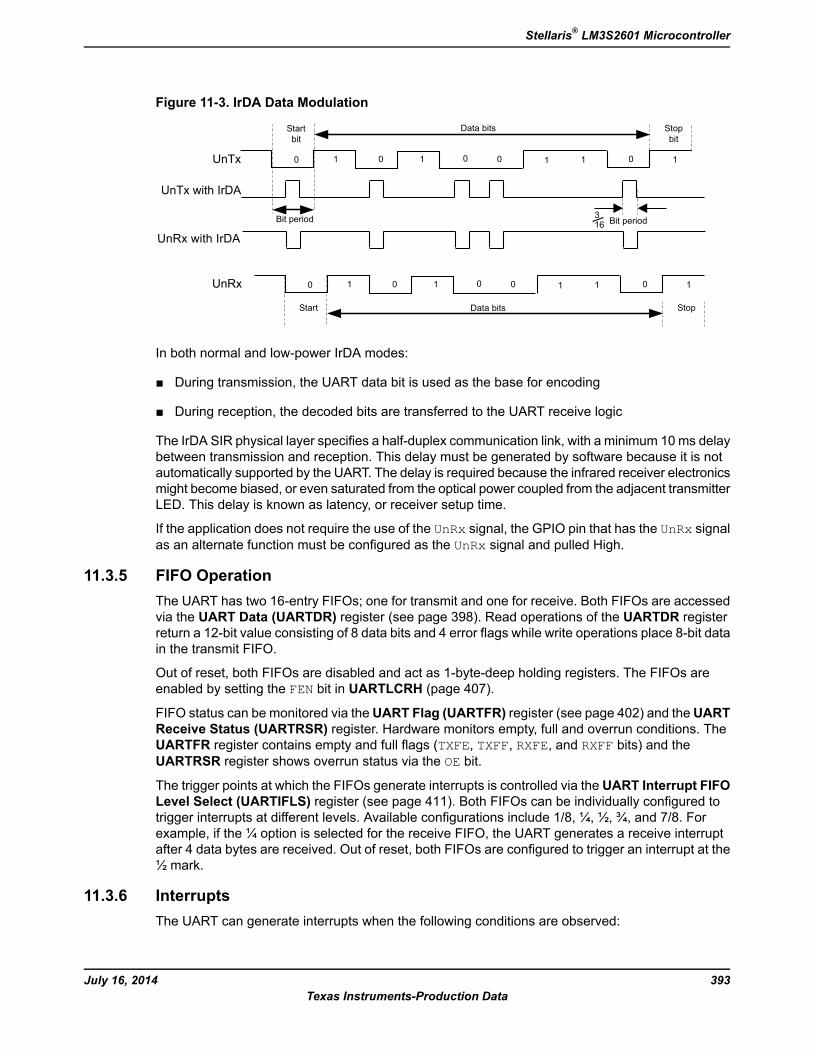
Figure 11-3. IrDA Data Modulation
10 10 0 0 1 1 0 1
Data bits
10 10 0 0 1 1 0 1
Data bitsStartbit
Start Stop
Bit period Bit period316
UnTx
UnTx with IrDA
UnRx with IrDA
UnRx
Stopbit
In both normal and low-power IrDA modes:
During transmission, the UART data bit is used as the base for encoding
During reception, the decoded bits are transferred to the UART receive logic
The IrDA SIR physical layer specifies a half-duplex communication link, with a minimum 10 ms delaybetween transmission and reception. This delay must be generated by software because it is notautomatically supported by the UART. The delay is required because the infrared receiver electronicsmight become biased, or even saturated from the optical power coupled from the adjacent transmitterLED. This delay is known as latency, or receiver setup time.
If the application does not require the use of the UnRx signal, the GPIO pin that has the UnRx signalas an alternate function must be configured as the UnRx signal and pulled High.
11.3.5 FIFO OperationThe UART has two 16-entry FIFOs; one for transmit and one for receive. Both FIFOs are accessedvia the UART Data (UARTDR) register (see page 398). Read operations of the UARTDR registerreturn a 12-bit value consisting of 8 data bits and 4 error flags while write operations place 8-bit datain the transmit FIFO.
Out of reset, both FIFOs are disabled and act as 1-byte-deep holding registers. The FIFOs areenabled by setting the FEN bit in UARTLCRH (page 407).
FIFO status can be monitored via theUART Flag (UARTFR) register (see page 402) and theUARTReceive Status (UARTRSR) register. Hardware monitors empty, full and overrun conditions. TheUARTFR register contains empty and full flags (TXFE, TXFF, RXFE, and RXFF bits) and theUARTRSR register shows overrun status via the OE bit.
The trigger points at which the FIFOs generate interrupts is controlled via the UART Interrupt FIFOLevel Select (UARTIFLS) register (see page 411). Both FIFOs can be individually configured totrigger interrupts at different levels. Available configurations include 1/8, ¼, ½, ¾, and 7/8. Forexample, if the ¼ option is selected for the receive FIFO, the UART generates a receive interruptafter 4 data bytes are received. Out of reset, both FIFOs are configured to trigger an interrupt at the½ mark.
11.3.6 InterruptsThe UART can generate interrupts when the following conditions are observed:
393July 16, 2014Texas Instruments-Production Data
Stellaris® LM3S2601 Microcontroller
Overrun Error
Break Error
Parity Error
Framing Error
Receive Timeout
Transmit (when condition defined in the TXIFLSEL bit in the UARTIFLS register is met)
Receive (when condition defined in the RXIFLSEL bit in the UARTIFLS register is met)
All of the interrupt events are ORed together before being sent to the interrupt controller, so theUART can only generate a single interrupt request to the controller at any given time. Software canservice multiple interrupt events in a single interrupt service routine by reading the UART MaskedInterrupt Status (UARTMIS) register (see page 416).
The interrupt events that can trigger a controller-level interrupt are defined in the UART InterruptMask (UARTIM ) register (see page 413) by setting the corresponding IM bit to 1. If interrupts arenot used, the raw interrupt status is always visible via the UART Raw Interrupt Status (UARTRIS)register (see page 415).
Interrupts are always cleared (for both the UARTMIS and UARTRIS registers) by setting thecorresponding bit in the UART Interrupt Clear (UARTICR) register (see page 417).
The receive interrupt changes state when one of the following events occurs:
If the FIFOs are enabled and the receive FIFO reaches the programmed trigger level, the RXRISbit is set. The receive interrupt is cleared by reading data from the receive FIFO until it becomesless than the trigger level, or by clearing the interrupt by writing a 1 to the RXIC bit.
If the FIFOs are disabled (have a depth of one location) and data is received thereby filling thelocation, the RXRIS bit is set. The receive interrupt is cleared by performing a single read of thereceive FIFO, or by clearing the interrupt by writing a 1 to the RXIC bit.
The transmit interrupt changes state when one of the following events occurs:
If the FIFOs are enabled and the transmit FIFO progresses through the programmed triggerlevel, the TXRIS bit is set. The transmit interrupt is based on a transition through level, thereforethe FIFOmust be written past the programmed trigger level otherwise no further transmit interruptswill be generated. The transmit interrupt is cleared by writing data to the transmit FIFO until itbecomes greater than the trigger level, or by clearing the interrupt by writing a 1 to the TXIC bit.
If the FIFOs are disabled (have a depth of one location) and there is no data present in thetransmitters single location, the TXRIS bit is set. It is cleared by performing a single write to thetransmit FIFO, or by clearing the interrupt by writing a 1 to the TXIC bit.
11.3.7 Loopback OperationThe UART can be placed into an internal loopback mode for diagnostic or debug work. This isaccomplished by setting the LBE bit in the UARTCTL register (see page 409). In loopback mode,data transmitted on UnTx is received on the UnRx input.
July 16, 2014394Texas Instruments-Production Data
Universal Asynchronous Receivers/Transmitters (UARTs)
11.3.8 IrDA SIR blockThe IrDA SIR block contains an IrDA serial IR (SIR) protocol encoder/decoder. When enabled, theSIR block uses the UnTx and UnRx pins for the SIR protocol, which should be connected to an IRtransceiver.
The SIR block can receive and transmit, but it is only half-duplex so it cannot do both at the sametime. Transmission must be stopped before data can be received. The IrDA SIR physical layerspecifies a minimum 10-ms delay between transmission and reception.
11.4 Initialization and ConfigurationTo use the UARTs, the peripheral clock must be enabled by setting the UART0, UART1, or UART2bits in the RCGC1 register.
This section discusses the steps that are required to use a UART module. For this example, theUART clock is assumed to be 20 MHz and the desired UART configuration is:
115200 baud rate
Data length of 8 bits
One stop bit
No parity
FIFOs disabled
No interrupts
The first thing to consider when programming the UART is the baud-rate divisor (BRD), since theUARTIBRD and UARTFBRD registers must be written before the UARTLCRH register. Using theequation described in “Baud-Rate Generation” on page 391, the BRD can be calculated:
BRD = 20,000,000 / (16 * 115,200) = 10.8507
which means that the DIVINT field of the UARTIBRD register (see page 405) should be set to 10.The value to be loaded into the UARTFBRD register (see page 406) is calculated by the equation:
UARTFBRD[DIVFRAC] = integer(0.8507 * 64 + 0.5) = 54
With the BRD values in hand, the UART configuration is written to the module in the following order:
1. Disable the UART by clearing the UARTEN bit in the UARTCTL register.
2. Write the integer portion of the BRD to the UARTIBRD register.
3. Write the fractional portion of the BRD to the UARTFBRD register.
4. Write the desired serial parameters to the UARTLCRH register (in this case, a value of0x0000.0060).
5. Enable the UART by setting the UARTEN bit in the UARTCTL register.
395July 16, 2014Texas Instruments-Production Data
Stellaris® LM3S2601 Microcontroller
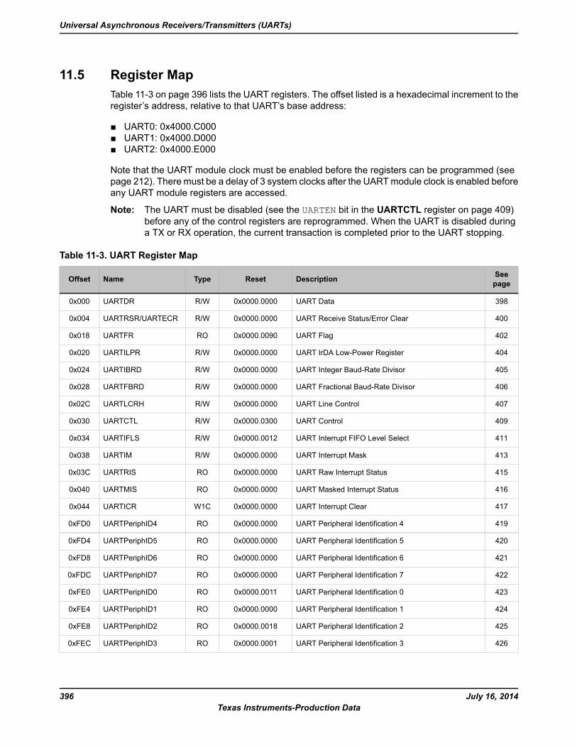
11.5 Register MapTable 11-3 on page 396 lists the UART registers. The offset listed is a hexadecimal increment to theregister’s address, relative to that UART’s base address:
UART0: 0x4000.C000 UART1: 0x4000.D000 UART2: 0x4000.E000
Note that the UART module clock must be enabled before the registers can be programmed (seepage 212). There must be a delay of 3 system clocks after the UARTmodule clock is enabled beforeany UART module registers are accessed.
Note: The UART must be disabled (see the UARTEN bit in the UARTCTL register on page 409)before any of the control registers are reprogrammed. When the UART is disabled duringa TX or RX operation, the current transaction is completed prior to the UART stopping.
Table 11-3. UART Register Map
SeepageDescriptionResetTypeNameOffset
398UART Data0x0000.0000R/WUARTDR0x000
400UART Receive Status/Error Clear0x0000.0000R/WUARTRSR/UARTECR0x004
402UART Flag0x0000.0090ROUARTFR0x018
404UART IrDA Low-Power Register0x0000.0000R/WUARTILPR0x020
405UART Integer Baud-Rate Divisor0x0000.0000R/WUARTIBRD0x024
406UART Fractional Baud-Rate Divisor0x0000.0000R/WUARTFBRD0x028
407UART Line Control0x0000.0000R/WUARTLCRH0x02C
409UART Control0x0000.0300R/WUARTCTL0x030
411UART Interrupt FIFO Level Select0x0000.0012R/WUARTIFLS0x034
413UART Interrupt Mask0x0000.0000R/WUARTIM0x038
415UART Raw Interrupt Status0x0000.0000ROUARTRIS0x03C
416UART Masked Interrupt Status0x0000.0000ROUARTMIS0x040
417UART Interrupt Clear0x0000.0000W1CUARTICR0x044
419UART Peripheral Identification 40x0000.0000ROUARTPeriphID40xFD0
420UART Peripheral Identification 50x0000.0000ROUARTPeriphID50xFD4
421UART Peripheral Identification 60x0000.0000ROUARTPeriphID60xFD8
422UART Peripheral Identification 70x0000.0000ROUARTPeriphID70xFDC
423UART Peripheral Identification 00x0000.0011ROUARTPeriphID00xFE0
424UART Peripheral Identification 10x0000.0000ROUARTPeriphID10xFE4
425UART Peripheral Identification 20x0000.0018ROUARTPeriphID20xFE8
426UART Peripheral Identification 30x0000.0001ROUARTPeriphID30xFEC
July 16, 2014396Texas Instruments-Production Data
Universal Asynchronous Receivers/Transmitters (UARTs)
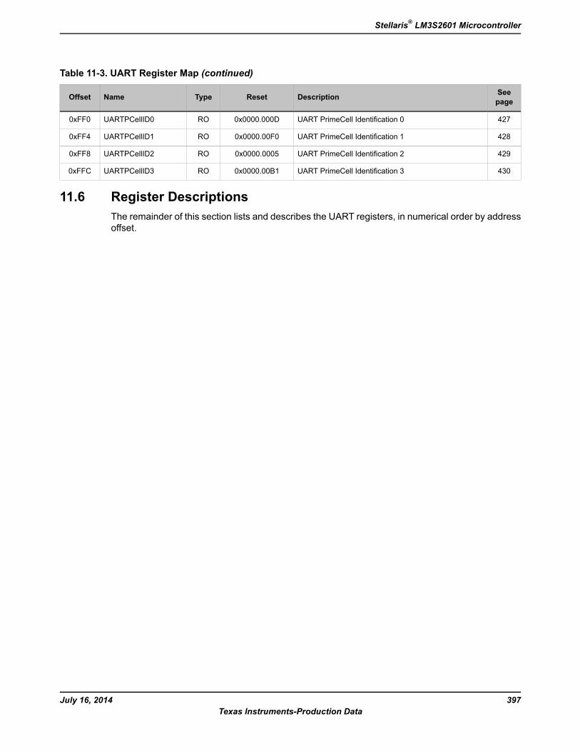
Table 11-3. UART Register Map (continued)
SeepageDescriptionResetTypeNameOffset
427UART PrimeCell Identification 00x0000.000DROUARTPCellID00xFF0
428UART PrimeCell Identification 10x0000.00F0ROUARTPCellID10xFF4
429UART PrimeCell Identification 20x0000.0005ROUARTPCellID20xFF8
430UART PrimeCell Identification 30x0000.00B1ROUARTPCellID30xFFC
11.6 Register DescriptionsThe remainder of this section lists and describes the UART registers, in numerical order by addressoffset.
397July 16, 2014Texas Instruments-Production Data
Stellaris® LM3S2601 Microcontroller
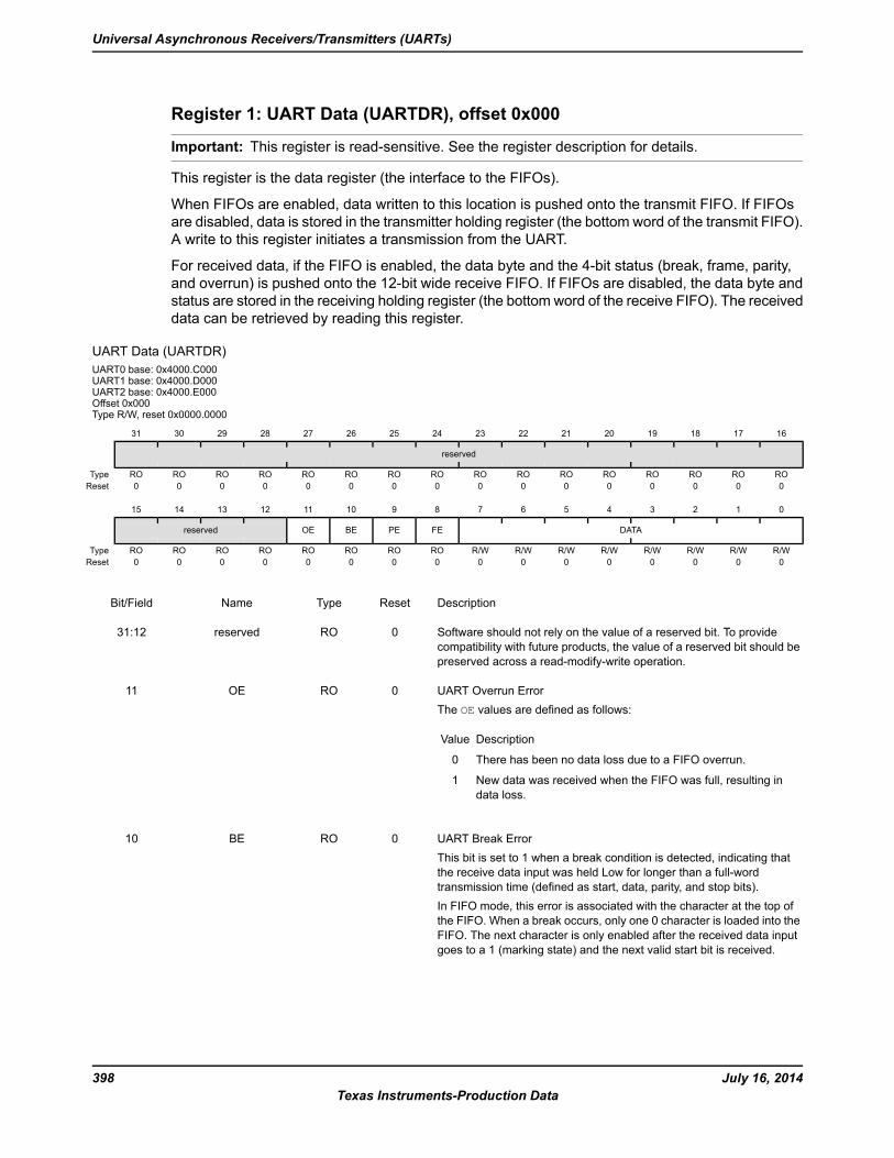
Register 1: UART Data (UARTDR), offset 0x000
Important: This register is read-sensitive. See the register description for details.
This register is the data register (the interface to the FIFOs).
When FIFOs are enabled, data written to this location is pushed onto the transmit FIFO. If FIFOsare disabled, data is stored in the transmitter holding register (the bottom word of the transmit FIFO).A write to this register initiates a transmission from the UART.
For received data, if the FIFO is enabled, the data byte and the 4-bit status (break, frame, parity,and overrun) is pushed onto the 12-bit wide receive FIFO. If FIFOs are disabled, the data byte andstatus are stored in the receiving holding register (the bottom word of the receive FIFO). The receiveddata can be retrieved by reading this register.
UART Data (UARTDR)UART0 base: 0x4000.C000UART1 base: 0x4000.D000UART2 base: 0x4000.E000Offset 0x000Type R/W, reset 0x0000.0000
16171819202122232425262728293031
reserved
ROROROROROROROROROROROROROROROROType0000000000000000Reset
0123456789101112131415
DATAFEPEBEOEreserved
R/WR/WR/WR/WR/WR/WR/WR/WROROROROROROROROType0000000000000000Reset
DescriptionResetTypeNameBit/Field
Software should not rely on the value of a reserved bit. To providecompatibility with future products, the value of a reserved bit should bepreserved across a read-modify-write operation.
0ROreserved31:12
UART Overrun ErrorThe OE values are defined as follows:
DescriptionValue
There has been no data loss due to a FIFO overrun.0
New data was received when the FIFO was full, resulting indata loss.
1
0ROOE11
UART Break ErrorThis bit is set to 1 when a break condition is detected, indicating thatthe receive data input was held Low for longer than a full-wordtransmission time (defined as start, data, parity, and stop bits).In FIFO mode, this error is associated with the character at the top ofthe FIFO. When a break occurs, only one 0 character is loaded into theFIFO. The next character is only enabled after the received data inputgoes to a 1 (marking state) and the next valid start bit is received.
0ROBE10
July 16, 2014398Texas Instruments-Production Data
Universal Asynchronous Receivers/Transmitters (UARTs)
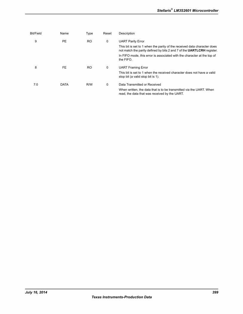
DescriptionResetTypeNameBit/Field
UART Parity ErrorThis bit is set to 1 when the parity of the received data character doesnot match the parity defined by bits 2 and 7 of the UARTLCRH register.In FIFO mode, this error is associated with the character at the top ofthe FIFO.
0ROPE9
UART Framing ErrorThis bit is set to 1 when the received character does not have a validstop bit (a valid stop bit is 1).
0ROFE8
Data Transmitted or ReceivedWhen written, the data that is to be transmitted via the UART. Whenread, the data that was received by the UART.
0R/WDATA7:0
399July 16, 2014Texas Instruments-Production Data
Stellaris® LM3S2601 Microcontroller
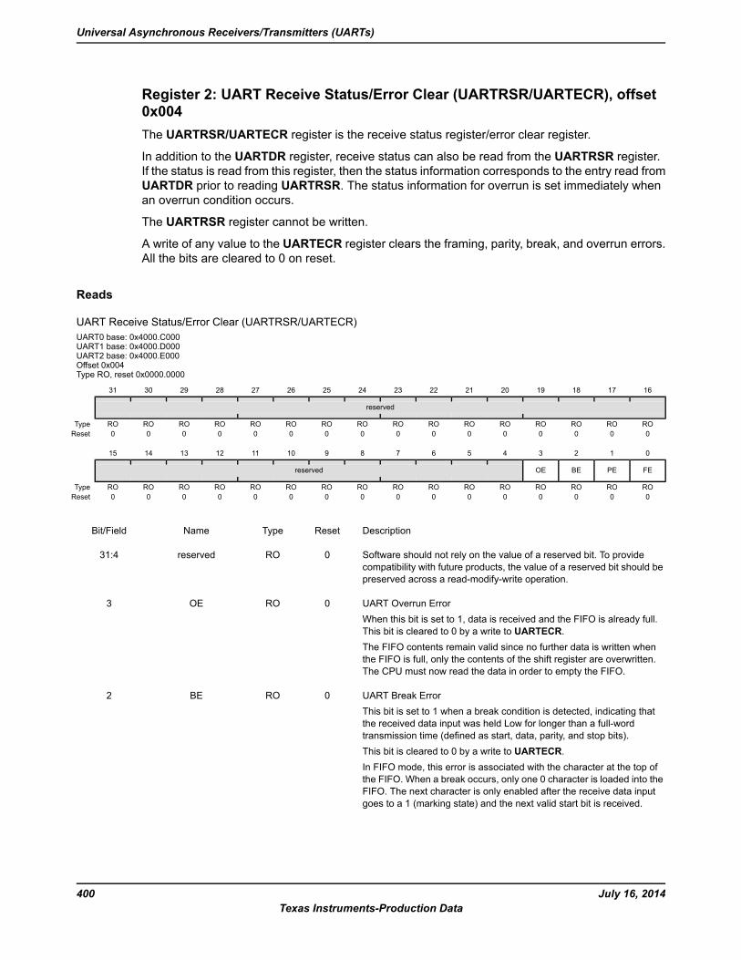
Register 2: UART Receive Status/Error Clear (UARTRSR/UARTECR), offset0x004The UARTRSR/UARTECR register is the receive status register/error clear register.
In addition to the UARTDR register, receive status can also be read from the UARTRSR register.If the status is read from this register, then the status information corresponds to the entry read fromUARTDR prior to reading UARTRSR. The status information for overrun is set immediately whenan overrun condition occurs.
The UARTRSR register cannot be written.
A write of any value to the UARTECR register clears the framing, parity, break, and overrun errors.All the bits are cleared to 0 on reset.
Reads
UART Receive Status/Error Clear (UARTRSR/UARTECR)UART0 base: 0x4000.C000UART1 base: 0x4000.D000UART2 base: 0x4000.E000Offset 0x004Type RO, reset 0x0000.0000
16171819202122232425262728293031
reserved
ROROROROROROROROROROROROROROROROType0000000000000000Reset
0123456789101112131415
FEPEBEOEreserved
ROROROROROROROROROROROROROROROROType0000000000000000Reset
DescriptionResetTypeNameBit/Field
Software should not rely on the value of a reserved bit. To providecompatibility with future products, the value of a reserved bit should bepreserved across a read-modify-write operation.
0ROreserved31:4
UART Overrun ErrorWhen this bit is set to 1, data is received and the FIFO is already full.This bit is cleared to 0 by a write to UARTECR.The FIFO contents remain valid since no further data is written whenthe FIFO is full, only the contents of the shift register are overwritten.The CPU must now read the data in order to empty the FIFO.
0ROOE3
UART Break ErrorThis bit is set to 1 when a break condition is detected, indicating thatthe received data input was held Low for longer than a full-wordtransmission time (defined as start, data, parity, and stop bits).This bit is cleared to 0 by a write to UARTECR.In FIFO mode, this error is associated with the character at the top ofthe FIFO. When a break occurs, only one 0 character is loaded into theFIFO. The next character is only enabled after the receive data inputgoes to a 1 (marking state) and the next valid start bit is received.
0ROBE2
July 16, 2014400Texas Instruments-Production Data
Universal Asynchronous Receivers/Transmitters (UARTs)
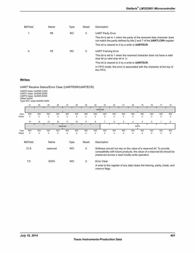
DescriptionResetTypeNameBit/Field
UART Parity ErrorThis bit is set to 1 when the parity of the received data character doesnot match the parity defined by bits 2 and 7 of the UARTLCRH register.This bit is cleared to 0 by a write to UARTECR.
0ROPE1
UART Framing ErrorThis bit is set to 1 when the received character does not have a validstop bit (a valid stop bit is 1).This bit is cleared to 0 by a write to UARTECR.In FIFO mode, this error is associated with the character at the top ofthe FIFO.
0ROFE0
Writes
UART Receive Status/Error Clear (UARTRSR/UARTECR)UART0 base: 0x4000.C000UART1 base: 0x4000.D000UART2 base: 0x4000.E000Offset 0x004Type WO, reset 0x0000.0000
16171819202122232425262728293031
reserved
WOWOWOWOWOWOWOWOWOWOWOWOWOWOWOWOType0000000000000000Reset
0123456789101112131415
DATAreserved
WOWOWOWOWOWOWOWOWOWOWOWOWOWOWOWOType0000000000000000Reset
DescriptionResetTypeNameBit/Field
Software should not rely on the value of a reserved bit. To providecompatibility with future products, the value of a reserved bit should bepreserved across a read-modify-write operation.
0WOreserved31:8
Error ClearA write to this register of any data clears the framing, parity, break, andoverrun flags.
0WODATA7:0
401July 16, 2014Texas Instruments-Production Data
Stellaris® LM3S2601 Microcontroller
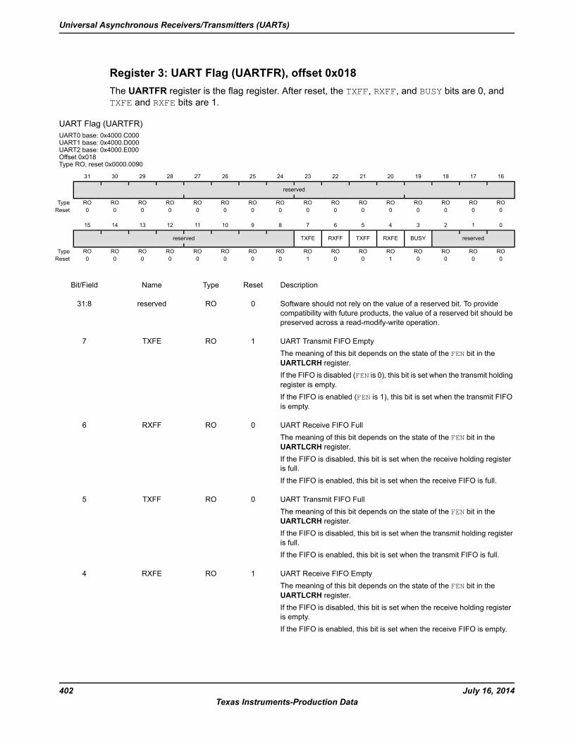
Register 3: UART Flag (UARTFR), offset 0x018The UARTFR register is the flag register. After reset, the TXFF, RXFF, and BUSY bits are 0, andTXFE and RXFE bits are 1.
UART Flag (UARTFR)UART0 base: 0x4000.C000UART1 base: 0x4000.D000UART2 base: 0x4000.E000Offset 0x018Type RO, reset 0x0000.0090
16171819202122232425262728293031
reserved
ROROROROROROROROROROROROROROROROType0000000000000000Reset
0123456789101112131415
reservedBUSYRXFETXFFRXFFTXFEreserved
ROROROROROROROROROROROROROROROROType0000100100000000Reset
DescriptionResetTypeNameBit/Field
Software should not rely on the value of a reserved bit. To providecompatibility with future products, the value of a reserved bit should bepreserved across a read-modify-write operation.
0ROreserved31:8
UART Transmit FIFO EmptyThe meaning of this bit depends on the state of the FEN bit in theUARTLCRH register.If the FIFO is disabled (FEN is 0), this bit is set when the transmit holdingregister is empty.If the FIFO is enabled (FEN is 1), this bit is set when the transmit FIFOis empty.
1ROTXFE7
UART Receive FIFO FullThe meaning of this bit depends on the state of the FEN bit in theUARTLCRH register.If the FIFO is disabled, this bit is set when the receive holding registeris full.If the FIFO is enabled, this bit is set when the receive FIFO is full.
0RORXFF6
UART Transmit FIFO FullThe meaning of this bit depends on the state of the FEN bit in theUARTLCRH register.If the FIFO is disabled, this bit is set when the transmit holding registeris full.If the FIFO is enabled, this bit is set when the transmit FIFO is full.
0ROTXFF5
UART Receive FIFO EmptyThe meaning of this bit depends on the state of the FEN bit in theUARTLCRH register.If the FIFO is disabled, this bit is set when the receive holding registeris empty.If the FIFO is enabled, this bit is set when the receive FIFO is empty.
1RORXFE4
July 16, 2014402Texas Instruments-Production Data
Universal Asynchronous Receivers/Transmitters (UARTs)
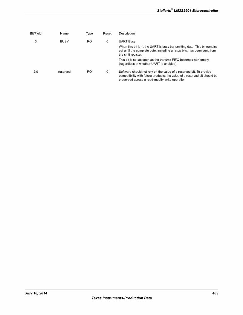
DescriptionResetTypeNameBit/Field
UART BusyWhen this bit is 1, the UART is busy transmitting data. This bit remainsset until the complete byte, including all stop bits, has been sent fromthe shift register.This bit is set as soon as the transmit FIFO becomes non-empty(regardless of whether UART is enabled).
0ROBUSY3
Software should not rely on the value of a reserved bit. To providecompatibility with future products, the value of a reserved bit should bepreserved across a read-modify-write operation.
0ROreserved2:0
403July 16, 2014Texas Instruments-Production Data
Stellaris® LM3S2601 Microcontroller
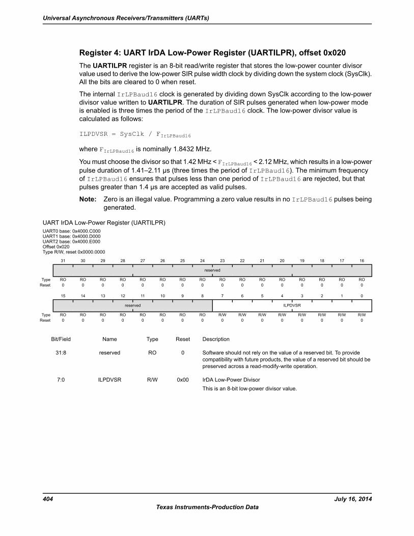
Register 4: UART IrDA Low-Power Register (UARTILPR), offset 0x020The UARTILPR register is an 8-bit read/write register that stores the low-power counter divisorvalue used to derive the low-power SIR pulse width clock by dividing down the system clock (SysClk).All the bits are cleared to 0 when reset.
The internal IrLPBaud16 clock is generated by dividing down SysClk according to the low-powerdivisor value written to UARTILPR. The duration of SIR pulses generated when low-power modeis enabled is three times the period of the IrLPBaud16 clock. The low-power divisor value iscalculated as follows:
ILPDVSR = SysClk / FIrLPBaud16
where FIrLPBaud16 is nominally 1.8432 MHz.
Youmust choose the divisor so that 1.42 MHz < FIrLPBaud16 < 2.12 MHz, which results in a low-powerpulse duration of 1.41–2.11 μs (three times the period of IrLPBaud16). The minimum frequencyof IrLPBaud16 ensures that pulses less than one period of IrLPBaud16 are rejected, but thatpulses greater than 1.4 μs are accepted as valid pulses.
Note: Zero is an illegal value. Programming a zero value results in no IrLPBaud16 pulses beinggenerated.
UART IrDA Low-Power Register (UARTILPR)UART0 base: 0x4000.C000UART1 base: 0x4000.D000UART2 base: 0x4000.E000Offset 0x020Type R/W, reset 0x0000.0000
16171819202122232425262728293031
reserved
ROROROROROROROROROROROROROROROROType0000000000000000Reset
0123456789101112131415
ILPDVSRreserved
R/WR/WR/WR/WR/WR/WR/WR/WROROROROROROROROType0000000000000000Reset
DescriptionResetTypeNameBit/Field
Software should not rely on the value of a reserved bit. To providecompatibility with future products, the value of a reserved bit should bepreserved across a read-modify-write operation.
0ROreserved31:8
IrDA Low-Power DivisorThis is an 8-bit low-power divisor value.
0x00R/WILPDVSR7:0
July 16, 2014404Texas Instruments-Production Data
Universal Asynchronous Receivers/Transmitters (UARTs)
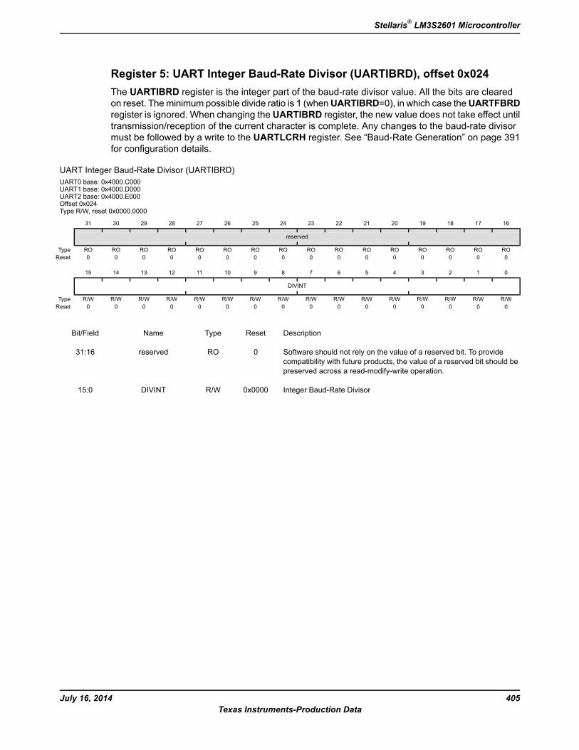
Register 5: UART Integer Baud-Rate Divisor (UARTIBRD), offset 0x024The UARTIBRD register is the integer part of the baud-rate divisor value. All the bits are clearedon reset. Theminimum possible divide ratio is 1 (whenUARTIBRD=0), in which case theUARTFBRDregister is ignored. When changing the UARTIBRD register, the new value does not take effect untiltransmission/reception of the current character is complete. Any changes to the baud-rate divisormust be followed by a write to the UARTLCRH register. See “Baud-Rate Generation” on page 391for configuration details.
UART Integer Baud-Rate Divisor (UARTIBRD)UART0 base: 0x4000.C000UART1 base: 0x4000.D000UART2 base: 0x4000.E000Offset 0x024Type R/W, reset 0x0000.0000
16171819202122232425262728293031
reserved
ROROROROROROROROROROROROROROROROType0000000000000000Reset
0123456789101112131415
DIVINT
R/WR/WR/WR/WR/WR/WR/WR/WR/WR/WR/WR/WR/WR/WR/WR/WType0000000000000000Reset
DescriptionResetTypeNameBit/Field
Software should not rely on the value of a reserved bit. To providecompatibility with future products, the value of a reserved bit should bepreserved across a read-modify-write operation.
0ROreserved31:16
Integer Baud-Rate Divisor0x0000R/WDIVINT15:0
405July 16, 2014Texas Instruments-Production Data
Stellaris® LM3S2601 Microcontroller
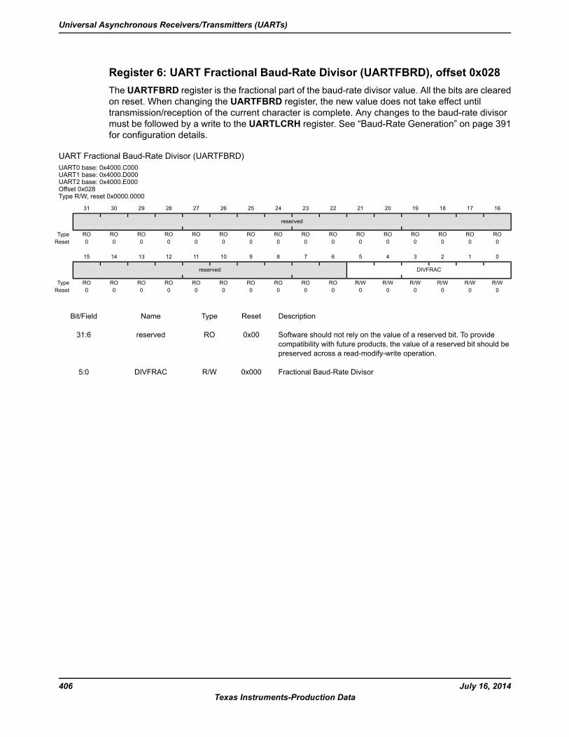
Register 6: UART Fractional Baud-Rate Divisor (UARTFBRD), offset 0x028The UARTFBRD register is the fractional part of the baud-rate divisor value. All the bits are clearedon reset. When changing the UARTFBRD register, the new value does not take effect untiltransmission/reception of the current character is complete. Any changes to the baud-rate divisormust be followed by a write to the UARTLCRH register. See “Baud-Rate Generation” on page 391for configuration details.
UART Fractional Baud-Rate Divisor (UARTFBRD)UART0 base: 0x4000.C000UART1 base: 0x4000.D000UART2 base: 0x4000.E000Offset 0x028Type R/W, reset 0x0000.0000
16171819202122232425262728293031
reserved
ROROROROROROROROROROROROROROROROType0000000000000000Reset
0123456789101112131415
DIVFRACreserved
R/WR/WR/WR/WR/WR/WROROROROROROROROROROType0000000000000000Reset
DescriptionResetTypeNameBit/Field
Software should not rely on the value of a reserved bit. To providecompatibility with future products, the value of a reserved bit should bepreserved across a read-modify-write operation.
0x00ROreserved31:6
Fractional Baud-Rate Divisor0x000R/WDIVFRAC5:0
July 16, 2014406Texas Instruments-Production Data
Universal Asynchronous Receivers/Transmitters (UARTs)
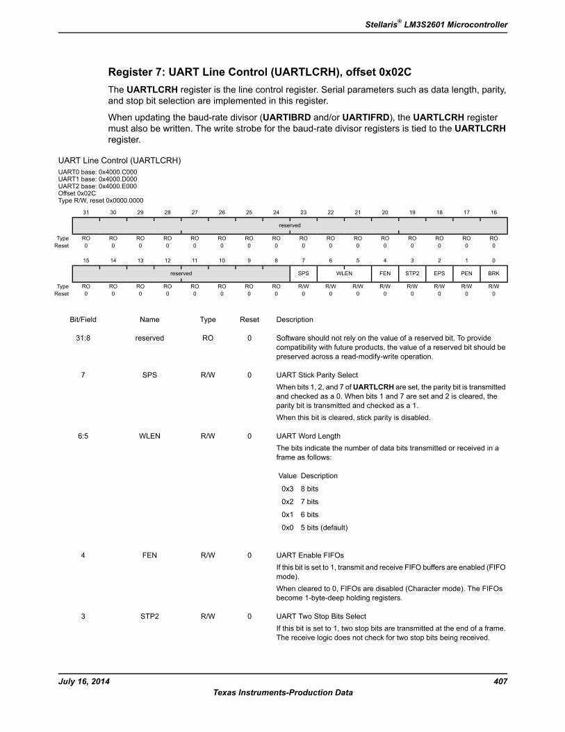
Register 7: UART Line Control (UARTLCRH), offset 0x02CThe UARTLCRH register is the line control register. Serial parameters such as data length, parity,and stop bit selection are implemented in this register.
When updating the baud-rate divisor (UARTIBRD and/or UARTIFRD), the UARTLCRH registermust also be written. The write strobe for the baud-rate divisor registers is tied to the UARTLCRHregister.
UART Line Control (UARTLCRH)UART0 base: 0x4000.C000UART1 base: 0x4000.D000UART2 base: 0x4000.E000Offset 0x02CType R/W, reset 0x0000.0000
16171819202122232425262728293031
reserved
ROROROROROROROROROROROROROROROROType0000000000000000Reset
0123456789101112131415
BRKPENEPSSTP2FENWLENSPSreserved
R/WR/WR/WR/WR/WR/WR/WR/WROROROROROROROROType0000000000000000Reset
DescriptionResetTypeNameBit/Field
Software should not rely on the value of a reserved bit. To providecompatibility with future products, the value of a reserved bit should bepreserved across a read-modify-write operation.
0ROreserved31:8
UART Stick Parity SelectWhen bits 1, 2, and 7 ofUARTLCRH are set, the parity bit is transmittedand checked as a 0. When bits 1 and 7 are set and 2 is cleared, theparity bit is transmitted and checked as a 1.When this bit is cleared, stick parity is disabled.
0R/WSPS7
UART Word LengthThe bits indicate the number of data bits transmitted or received in aframe as follows:
DescriptionValue
8 bits0x3
7 bits0x2
6 bits0x1
5 bits (default)0x0
0R/WWLEN6:5
UART Enable FIFOsIf this bit is set to 1, transmit and receive FIFO buffers are enabled (FIFOmode).When cleared to 0, FIFOs are disabled (Character mode). The FIFOsbecome 1-byte-deep holding registers.
0R/WFEN4
UART Two Stop Bits SelectIf this bit is set to 1, two stop bits are transmitted at the end of a frame.The receive logic does not check for two stop bits being received.
0R/WSTP23
407July 16, 2014Texas Instruments-Production Data
Stellaris® LM3S2601 Microcontroller
DescriptionResetTypeNameBit/Field
UART Even Parity SelectIf this bit is set to 1, even parity generation and checking is performedduring transmission and reception, which checks for an even numberof 1s in data and parity bits.When cleared to 0, then odd parity is performed, which checks for anodd number of 1s.This bit has no effect when parity is disabled by the PEN bit.
0R/WEPS2
UART Parity EnableIf this bit is set to 1, parity checking and generation is enabled; otherwise,parity is disabled and no parity bit is added to the data frame.
0R/WPEN1
UART Send BreakIf this bit is set to 1, a Low level is continually output on the UnTX output,after completing transmission of the current character. For the properexecution of the break command, the software must set this bit for atleast two frames (character periods). For normal use, this bit must becleared to 0.
0R/WBRK0
July 16, 2014408Texas Instruments-Production Data
Universal Asynchronous Receivers/Transmitters (UARTs)
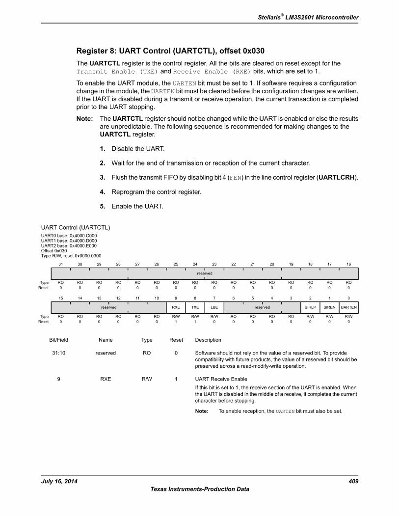
Register 8: UART Control (UARTCTL), offset 0x030The UARTCTL register is the control register. All the bits are cleared on reset except for theTransmit Enable (TXE) and Receive Enable (RXE) bits, which are set to 1.
To enable the UART module, the UARTEN bit must be set to 1. If software requires a configurationchange in the module, the UARTEN bit must be cleared before the configuration changes are written.If the UART is disabled during a transmit or receive operation, the current transaction is completedprior to the UART stopping.
Note: TheUARTCTL register should not be changed while the UART is enabled or else the resultsare unpredictable. The following sequence is recommended for making changes to theUARTCTL register.
1. Disable the UART.
2. Wait for the end of transmission or reception of the current character.
3. Flush the transmit FIFO by disabling bit 4 (FEN) in the line control register (UARTLCRH).
4. Reprogram the control register.
5. Enable the UART.
UART Control (UARTCTL)UART0 base: 0x4000.C000UART1 base: 0x4000.D000UART2 base: 0x4000.E000Offset 0x030Type R/W, reset 0x0000.0300
16171819202122232425262728293031
reserved
ROROROROROROROROROROROROROROROROType0000000000000000Reset
0123456789101112131415
UARTENSIRENSIRLPreservedLBETXERXEreserved
R/WR/WR/WROROROROR/WR/WR/WROROROROROROType0000000011000000Reset
DescriptionResetTypeNameBit/Field
Software should not rely on the value of a reserved bit. To providecompatibility with future products, the value of a reserved bit should bepreserved across a read-modify-write operation.
0ROreserved31:10
UART Receive EnableIf this bit is set to 1, the receive section of the UART is enabled. Whenthe UART is disabled in the middle of a receive, it completes the currentcharacter before stopping.
Note: To enable reception, the UARTEN bit must also be set.
1R/WRXE9
409July 16, 2014Texas Instruments-Production Data
Stellaris® LM3S2601 Microcontroller
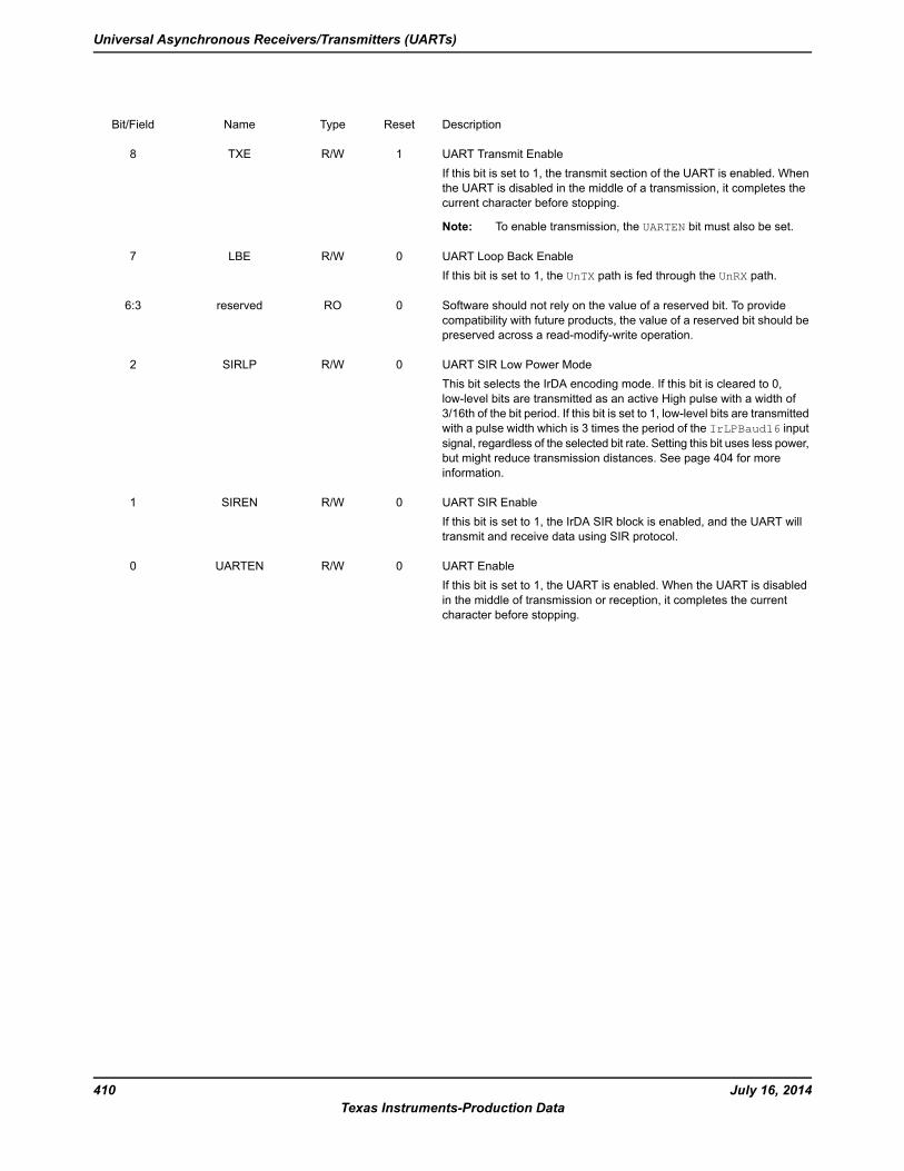
DescriptionResetTypeNameBit/Field
UART Transmit EnableIf this bit is set to 1, the transmit section of the UART is enabled. Whenthe UART is disabled in the middle of a transmission, it completes thecurrent character before stopping.
Note: To enable transmission, the UARTEN bit must also be set.
1R/WTXE8
UART Loop Back EnableIf this bit is set to 1, the UnTX path is fed through the UnRX path.
0R/WLBE7
Software should not rely on the value of a reserved bit. To providecompatibility with future products, the value of a reserved bit should bepreserved across a read-modify-write operation.
0ROreserved6:3
UART SIR Low Power ModeThis bit selects the IrDA encoding mode. If this bit is cleared to 0,low-level bits are transmitted as an active High pulse with a width of3/16th of the bit period. If this bit is set to 1, low-level bits are transmittedwith a pulse width which is 3 times the period of the IrLPBaud16 inputsignal, regardless of the selected bit rate. Setting this bit uses less power,but might reduce transmission distances. See page 404 for moreinformation.
0R/WSIRLP2
UART SIR EnableIf this bit is set to 1, the IrDA SIR block is enabled, and the UART willtransmit and receive data using SIR protocol.
0R/WSIREN1
UART EnableIf this bit is set to 1, the UART is enabled. When the UART is disabledin the middle of transmission or reception, it completes the currentcharacter before stopping.
0R/WUARTEN0
July 16, 2014410Texas Instruments-Production Data
Universal Asynchronous Receivers/Transmitters (UARTs)
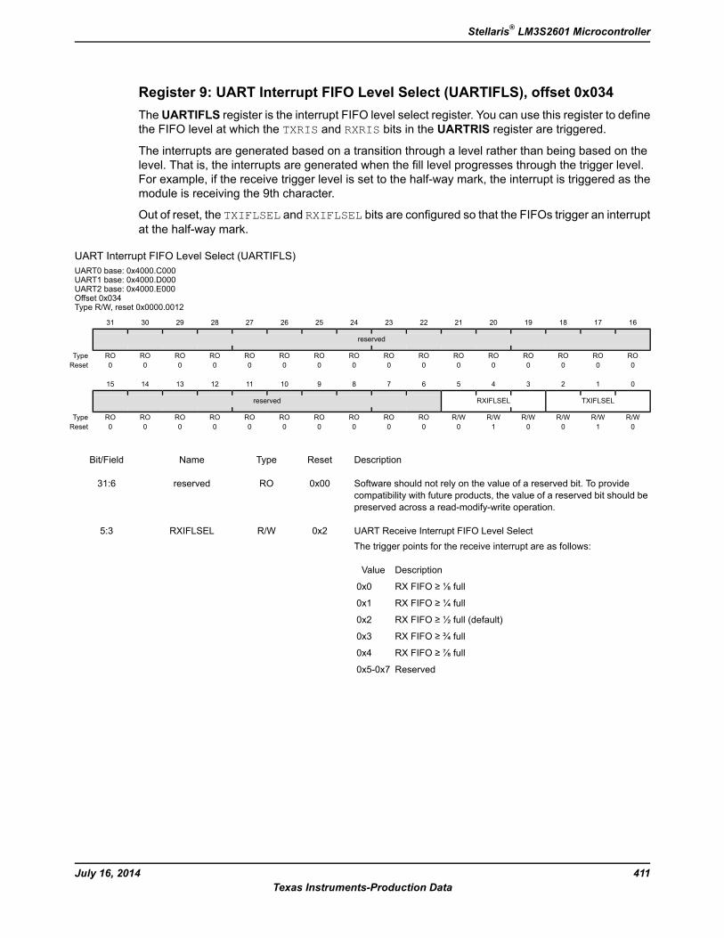
Register 9: UART Interrupt FIFO Level Select (UARTIFLS), offset 0x034The UARTIFLS register is the interrupt FIFO level select register. You can use this register to definethe FIFO level at which the TXRIS and RXRIS bits in the UARTRIS register are triggered.
The interrupts are generated based on a transition through a level rather than being based on thelevel. That is, the interrupts are generated when the fill level progresses through the trigger level.For example, if the receive trigger level is set to the half-way mark, the interrupt is triggered as themodule is receiving the 9th character.
Out of reset, the TXIFLSEL and RXIFLSEL bits are configured so that the FIFOs trigger an interruptat the half-way mark.
UART Interrupt FIFO Level Select (UARTIFLS)UART0 base: 0x4000.C000UART1 base: 0x4000.D000UART2 base: 0x4000.E000Offset 0x034Type R/W, reset 0x0000.0012
16171819202122232425262728293031
reserved
ROROROROROROROROROROROROROROROROType0000000000000000Reset
0123456789101112131415
TXIFLSELRXIFLSELreserved
R/WR/WR/WR/WR/WR/WROROROROROROROROROROType0100100000000000Reset
DescriptionResetTypeNameBit/Field
Software should not rely on the value of a reserved bit. To providecompatibility with future products, the value of a reserved bit should bepreserved across a read-modify-write operation.
0x00ROreserved31:6
UART Receive Interrupt FIFO Level SelectThe trigger points for the receive interrupt are as follows:
DescriptionValue
RX FIFO ≥ ⅛ full0x0
RX FIFO ≥ ¼ full0x1
RX FIFO ≥ ½ full (default)0x2
RX FIFO ≥ ¾ full0x3
RX FIFO ≥ ⅞ full0x4
Reserved0x5-0x7
0x2R/WRXIFLSEL5:3
411July 16, 2014Texas Instruments-Production Data
Stellaris® LM3S2601 Microcontroller
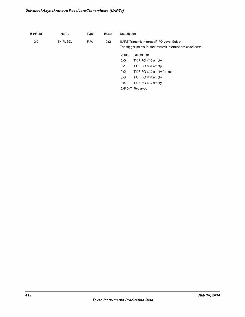
DescriptionResetTypeNameBit/Field
UART Transmit Interrupt FIFO Level SelectThe trigger points for the transmit interrupt are as follows:
DescriptionValue
TX FIFO ≤ ⅞ empty0x0
TX FIFO ≤ ¾ empty0x1
TX FIFO ≤ ½ empty (default)0x2
TX FIFO ≤ ¼ empty0x3
TX FIFO ≤ ⅛ empty0x4
Reserved0x5-0x7
0x2R/WTXIFLSEL2:0
July 16, 2014412Texas Instruments-Production Data
Universal Asynchronous Receivers/Transmitters (UARTs)
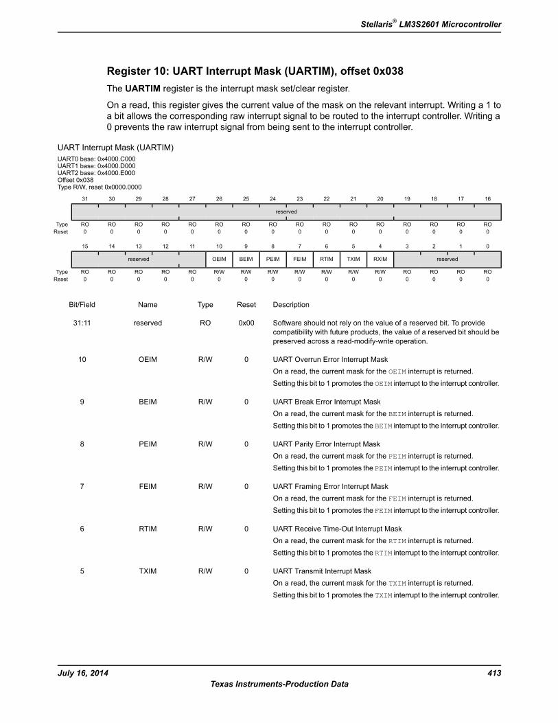
Register 10: UART Interrupt Mask (UARTIM), offset 0x038The UARTIM register is the interrupt mask set/clear register.
On a read, this register gives the current value of the mask on the relevant interrupt. Writing a 1 toa bit allows the corresponding raw interrupt signal to be routed to the interrupt controller. Writing a0 prevents the raw interrupt signal from being sent to the interrupt controller.
UART Interrupt Mask (UARTIM)UART0 base: 0x4000.C000UART1 base: 0x4000.D000UART2 base: 0x4000.E000Offset 0x038Type R/W, reset 0x0000.0000
16171819202122232425262728293031
reserved
ROROROROROROROROROROROROROROROROType0000000000000000Reset
0123456789101112131415
reservedRXIMTXIMRTIMFEIMPEIMBEIMOEIMreserved
ROROROROR/WR/WR/WR/WR/WR/WR/WROROROROROType0000000000000000Reset
DescriptionResetTypeNameBit/Field
Software should not rely on the value of a reserved bit. To providecompatibility with future products, the value of a reserved bit should bepreserved across a read-modify-write operation.
0x00ROreserved31:11
UART Overrun Error Interrupt MaskOn a read, the current mask for the OEIM interrupt is returned.Setting this bit to 1 promotes the OEIM interrupt to the interrupt controller.
0R/WOEIM10
UART Break Error Interrupt MaskOn a read, the current mask for the BEIM interrupt is returned.Setting this bit to 1 promotes the BEIM interrupt to the interrupt controller.
0R/WBEIM9
UART Parity Error Interrupt MaskOn a read, the current mask for the PEIM interrupt is returned.Setting this bit to 1 promotes the PEIM interrupt to the interrupt controller.
0R/WPEIM8
UART Framing Error Interrupt MaskOn a read, the current mask for the FEIM interrupt is returned.Setting this bit to 1 promotes the FEIM interrupt to the interrupt controller.
0R/WFEIM7
UART Receive Time-Out Interrupt MaskOn a read, the current mask for the RTIM interrupt is returned.Setting this bit to 1 promotes the RTIM interrupt to the interrupt controller.
0R/WRTIM6
UART Transmit Interrupt MaskOn a read, the current mask for the TXIM interrupt is returned.Setting this bit to 1 promotes the TXIM interrupt to the interrupt controller.
0R/WTXIM5
413July 16, 2014Texas Instruments-Production Data
Stellaris® LM3S2601 Microcontroller
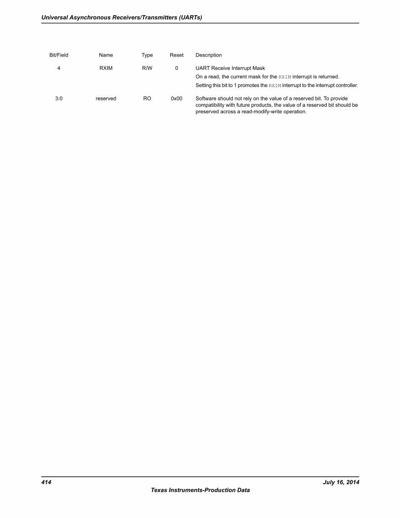
DescriptionResetTypeNameBit/Field
UART Receive Interrupt MaskOn a read, the current mask for the RXIM interrupt is returned.Setting this bit to 1 promotes the RXIM interrupt to the interrupt controller.
0R/WRXIM4
Software should not rely on the value of a reserved bit. To providecompatibility with future products, the value of a reserved bit should bepreserved across a read-modify-write operation.
0x00ROreserved3:0
July 16, 2014414Texas Instruments-Production Data
Universal Asynchronous Receivers/Transmitters (UARTs)
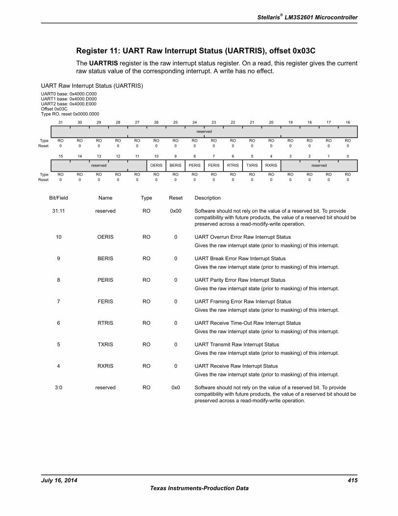
Register 11: UART Raw Interrupt Status (UARTRIS), offset 0x03CThe UARTRIS register is the raw interrupt status register. On a read, this register gives the currentraw status value of the corresponding interrupt. A write has no effect.
UART Raw Interrupt Status (UARTRIS)UART0 base: 0x4000.C000UART1 base: 0x4000.D000UART2 base: 0x4000.E000Offset 0x03CType RO, reset 0x0000.0000
16171819202122232425262728293031
reserved
ROROROROROROROROROROROROROROROROType0000000000000000Reset
0123456789101112131415
reservedRXRISTXRISRTRISFERISPERISBERISOERISreserved
ROROROROROROROROROROROROROROROROType0000000000000000Reset
DescriptionResetTypeNameBit/Field
Software should not rely on the value of a reserved bit. To providecompatibility with future products, the value of a reserved bit should bepreserved across a read-modify-write operation.
0x00ROreserved31:11
UART Overrun Error Raw Interrupt StatusGives the raw interrupt state (prior to masking) of this interrupt.
0ROOERIS10
UART Break Error Raw Interrupt StatusGives the raw interrupt state (prior to masking) of this interrupt.
0ROBERIS9
UART Parity Error Raw Interrupt StatusGives the raw interrupt state (prior to masking) of this interrupt.
0ROPERIS8
UART Framing Error Raw Interrupt StatusGives the raw interrupt state (prior to masking) of this interrupt.
0ROFERIS7
UART Receive Time-Out Raw Interrupt StatusGives the raw interrupt state (prior to masking) of this interrupt.
0RORTRIS6
UART Transmit Raw Interrupt StatusGives the raw interrupt state (prior to masking) of this interrupt.
0ROTXRIS5
UART Receive Raw Interrupt StatusGives the raw interrupt state (prior to masking) of this interrupt.
0RORXRIS4
Software should not rely on the value of a reserved bit. To providecompatibility with future products, the value of a reserved bit should bepreserved across a read-modify-write operation.
0x0ROreserved3:0
415July 16, 2014Texas Instruments-Production Data
Stellaris® LM3S2601 Microcontroller
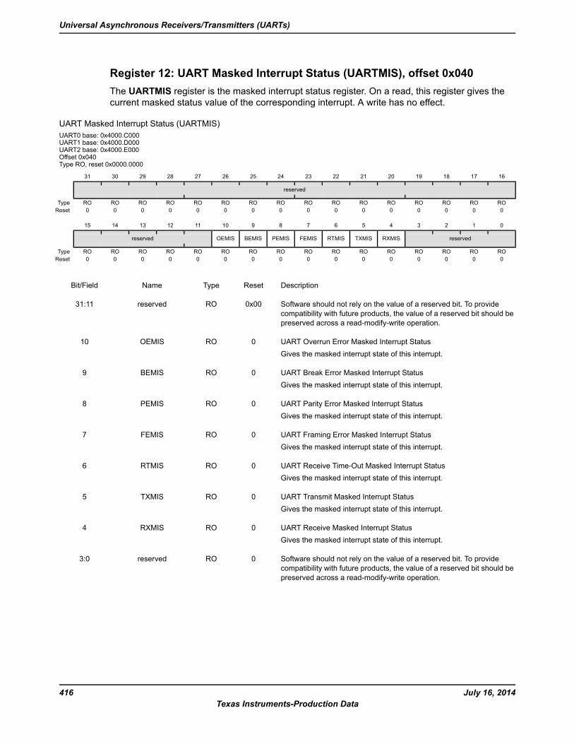
Register 12: UART Masked Interrupt Status (UARTMIS), offset 0x040The UARTMIS register is the masked interrupt status register. On a read, this register gives thecurrent masked status value of the corresponding interrupt. A write has no effect.
UART Masked Interrupt Status (UARTMIS)UART0 base: 0x4000.C000UART1 base: 0x4000.D000UART2 base: 0x4000.E000Offset 0x040Type RO, reset 0x0000.0000
16171819202122232425262728293031
reserved
ROROROROROROROROROROROROROROROROType0000000000000000Reset
0123456789101112131415
reservedRXMISTXMISRTMISFEMISPEMISBEMISOEMISreserved
ROROROROROROROROROROROROROROROROType0000000000000000Reset
DescriptionResetTypeNameBit/Field
Software should not rely on the value of a reserved bit. To providecompatibility with future products, the value of a reserved bit should bepreserved across a read-modify-write operation.
0x00ROreserved31:11
UART Overrun Error Masked Interrupt StatusGives the masked interrupt state of this interrupt.
0ROOEMIS10
UART Break Error Masked Interrupt StatusGives the masked interrupt state of this interrupt.
0ROBEMIS9
UART Parity Error Masked Interrupt StatusGives the masked interrupt state of this interrupt.
0ROPEMIS8
UART Framing Error Masked Interrupt StatusGives the masked interrupt state of this interrupt.
0ROFEMIS7
UART Receive Time-Out Masked Interrupt StatusGives the masked interrupt state of this interrupt.
0RORTMIS6
UART Transmit Masked Interrupt StatusGives the masked interrupt state of this interrupt.
0ROTXMIS5
UART Receive Masked Interrupt StatusGives the masked interrupt state of this interrupt.
0RORXMIS4
Software should not rely on the value of a reserved bit. To providecompatibility with future products, the value of a reserved bit should bepreserved across a read-modify-write operation.
0ROreserved3:0
July 16, 2014416Texas Instruments-Production Data
Universal Asynchronous Receivers/Transmitters (UARTs)
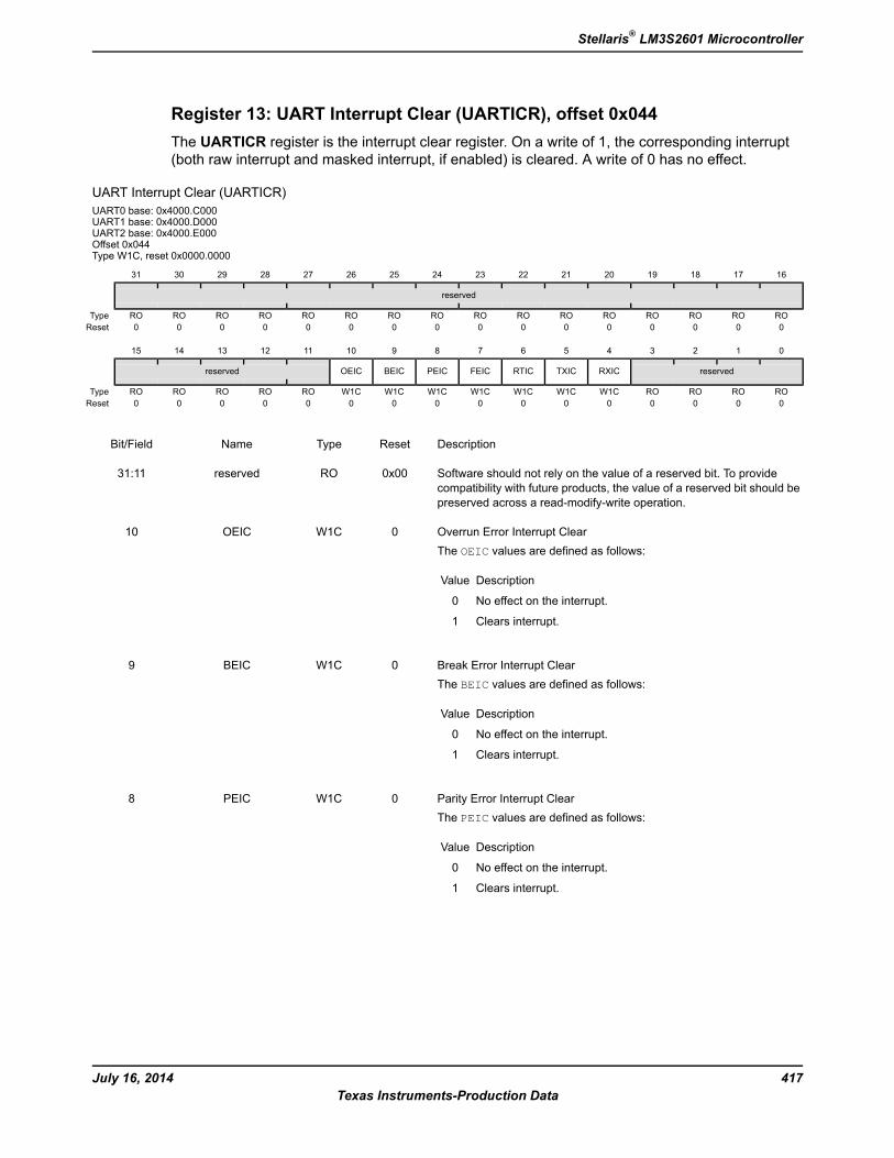
Register 13: UART Interrupt Clear (UARTICR), offset 0x044The UARTICR register is the interrupt clear register. On a write of 1, the corresponding interrupt(both raw interrupt and masked interrupt, if enabled) is cleared. A write of 0 has no effect.
UART Interrupt Clear (UARTICR)UART0 base: 0x4000.C000UART1 base: 0x4000.D000UART2 base: 0x4000.E000Offset 0x044Type W1C, reset 0x0000.0000
16171819202122232425262728293031
reserved
ROROROROROROROROROROROROROROROROType0000000000000000Reset
0123456789101112131415
reservedRXICTXICRTICFEICPEICBEICOEICreserved
ROROROROW1CW1CW1CW1CW1CW1CW1CROROROROROType0000000000000000Reset
DescriptionResetTypeNameBit/Field
Software should not rely on the value of a reserved bit. To providecompatibility with future products, the value of a reserved bit should bepreserved across a read-modify-write operation.
0x00ROreserved31:11
Overrun Error Interrupt ClearThe OEIC values are defined as follows:
DescriptionValue
No effect on the interrupt.0
Clears interrupt.1
0W1COEIC10
Break Error Interrupt ClearThe BEIC values are defined as follows:
DescriptionValue
No effect on the interrupt.0
Clears interrupt.1
0W1CBEIC9
Parity Error Interrupt ClearThe PEIC values are defined as follows:
DescriptionValue
No effect on the interrupt.0
Clears interrupt.1
0W1CPEIC8
417July 16, 2014Texas Instruments-Production Data
Stellaris® LM3S2601 Microcontroller
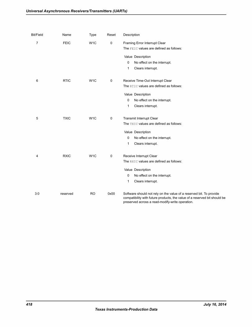
DescriptionResetTypeNameBit/Field
Framing Error Interrupt ClearThe FEIC values are defined as follows:
DescriptionValue
No effect on the interrupt.0
Clears interrupt.1
0W1CFEIC7
Receive Time-Out Interrupt ClearThe RTIC values are defined as follows:
DescriptionValue
No effect on the interrupt.0
Clears interrupt.1
0W1CRTIC6
Transmit Interrupt ClearThe TXIC values are defined as follows:
DescriptionValue
No effect on the interrupt.0
Clears interrupt.1
0W1CTXIC5
Receive Interrupt ClearThe RXIC values are defined as follows:
DescriptionValue
No effect on the interrupt.0
Clears interrupt.1
0W1CRXIC4
Software should not rely on the value of a reserved bit. To providecompatibility with future products, the value of a reserved bit should bepreserved across a read-modify-write operation.
0x00ROreserved3:0
July 16, 2014418Texas Instruments-Production Data
Universal Asynchronous Receivers/Transmitters (UARTs)

Register 14: UART Peripheral Identification 4 (UARTPeriphID4), offset 0xFD0The UARTPeriphIDn registers are hard-coded and the fields within the registers determine thereset values.
UART Peripheral Identification 4 (UARTPeriphID4)UART0 base: 0x4000.C000UART1 base: 0x4000.D000UART2 base: 0x4000.E000Offset 0xFD0Type RO, reset 0x0000.0000
16171819202122232425262728293031
reserved
ROROROROROROROROROROROROROROROROType0000000000000000Reset
0123456789101112131415
PID4reserved
ROROROROROROROROROROROROROROROROType0000000000000000Reset
DescriptionResetTypeNameBit/Field
Software should not rely on the value of a reserved bit. To providecompatibility with future products, the value of a reserved bit should bepreserved across a read-modify-write operation.
0x00ROreserved31:8
UART Peripheral ID Register[7:0]Can be used by software to identify the presence of this peripheral.
0x0000ROPID47:0
419July 16, 2014Texas Instruments-Production Data
Stellaris® LM3S2601 Microcontroller

Register 15: UART Peripheral Identification 5 (UARTPeriphID5), offset 0xFD4The UARTPeriphIDn registers are hard-coded and the fields within the registers determine thereset values.
UART Peripheral Identification 5 (UARTPeriphID5)UART0 base: 0x4000.C000UART1 base: 0x4000.D000UART2 base: 0x4000.E000Offset 0xFD4Type RO, reset 0x0000.0000
16171819202122232425262728293031
reserved
ROROROROROROROROROROROROROROROROType0000000000000000Reset
0123456789101112131415
PID5reserved
ROROROROROROROROROROROROROROROROType0000000000000000Reset
DescriptionResetTypeNameBit/Field
Software should not rely on the value of a reserved bit. To providecompatibility with future products, the value of a reserved bit should bepreserved across a read-modify-write operation.
0x00ROreserved31:8
UART Peripheral ID Register[15:8]Can be used by software to identify the presence of this peripheral.
0x0000ROPID57:0
July 16, 2014420Texas Instruments-Production Data
Universal Asynchronous Receivers/Transmitters (UARTs)

Register 16: UART Peripheral Identification 6 (UARTPeriphID6), offset 0xFD8The UARTPeriphIDn registers are hard-coded and the fields within the registers determine thereset values.
UART Peripheral Identification 6 (UARTPeriphID6)UART0 base: 0x4000.C000UART1 base: 0x4000.D000UART2 base: 0x4000.E000Offset 0xFD8Type RO, reset 0x0000.0000
16171819202122232425262728293031
reserved
ROROROROROROROROROROROROROROROROType0000000000000000Reset
0123456789101112131415
PID6reserved
ROROROROROROROROROROROROROROROROType0000000000000000Reset
DescriptionResetTypeNameBit/Field
Software should not rely on the value of a reserved bit. To providecompatibility with future products, the value of a reserved bit should bepreserved across a read-modify-write operation.
0x00ROreserved31:8
UART Peripheral ID Register[23:16]Can be used by software to identify the presence of this peripheral.
0x0000ROPID67:0
421July 16, 2014Texas Instruments-Production Data
Stellaris® LM3S2601 Microcontroller

Register 17: UART Peripheral Identification 7 (UARTPeriphID7), offset 0xFDCThe UARTPeriphIDn registers are hard-coded and the fields within the registers determine thereset values.
UART Peripheral Identification 7 (UARTPeriphID7)UART0 base: 0x4000.C000UART1 base: 0x4000.D000UART2 base: 0x4000.E000Offset 0xFDCType RO, reset 0x0000.0000
16171819202122232425262728293031
reserved
ROROROROROROROROROROROROROROROROType0000000000000000Reset
0123456789101112131415
PID7reserved
ROROROROROROROROROROROROROROROROType0000000000000000Reset
DescriptionResetTypeNameBit/Field
Software should not rely on the value of a reserved bit. To providecompatibility with future products, the value of a reserved bit should bepreserved across a read-modify-write operation.
0ROreserved31:8
UART Peripheral ID Register[31:24]Can be used by software to identify the presence of this peripheral.
0x0000ROPID77:0
July 16, 2014422Texas Instruments-Production Data
Universal Asynchronous Receivers/Transmitters (UARTs)

Register 18: UART Peripheral Identification 0 (UARTPeriphID0), offset 0xFE0The UARTPeriphIDn registers are hard-coded and the fields within the registers determine thereset values.
UART Peripheral Identification 0 (UARTPeriphID0)UART0 base: 0x4000.C000UART1 base: 0x4000.D000UART2 base: 0x4000.E000Offset 0xFE0Type RO, reset 0x0000.0011
16171819202122232425262728293031
reserved
ROROROROROROROROROROROROROROROROType0000000000000000Reset
0123456789101112131415
PID0reserved
ROROROROROROROROROROROROROROROROType1000100000000000Reset
DescriptionResetTypeNameBit/Field
Software should not rely on the value of a reserved bit. To providecompatibility with future products, the value of a reserved bit should bepreserved across a read-modify-write operation.
0x00ROreserved31:8
UART Peripheral ID Register[7:0]Can be used by software to identify the presence of this peripheral.
0x11ROPID07:0
423July 16, 2014Texas Instruments-Production Data
Stellaris® LM3S2601 Microcontroller

Register 19: UART Peripheral Identification 1 (UARTPeriphID1), offset 0xFE4The UARTPeriphIDn registers are hard-coded and the fields within the registers determine thereset values.
UART Peripheral Identification 1 (UARTPeriphID1)UART0 base: 0x4000.C000UART1 base: 0x4000.D000UART2 base: 0x4000.E000Offset 0xFE4Type RO, reset 0x0000.0000
16171819202122232425262728293031
reserved
ROROROROROROROROROROROROROROROROType0000000000000000Reset
0123456789101112131415
PID1reserved
ROROROROROROROROROROROROROROROROType0000000000000000Reset
DescriptionResetTypeNameBit/Field
Software should not rely on the value of a reserved bit. To providecompatibility with future products, the value of a reserved bit should bepreserved across a read-modify-write operation.
0x00ROreserved31:8
UART Peripheral ID Register[15:8]Can be used by software to identify the presence of this peripheral.
0x00ROPID17:0
July 16, 2014424Texas Instruments-Production Data
Universal Asynchronous Receivers/Transmitters (UARTs)
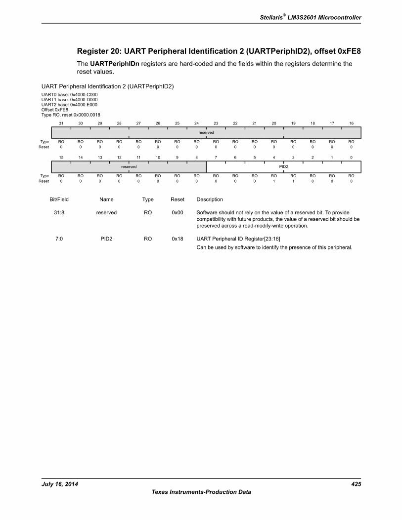
Register 20: UART Peripheral Identification 2 (UARTPeriphID2), offset 0xFE8The UARTPeriphIDn registers are hard-coded and the fields within the registers determine thereset values.
UART Peripheral Identification 2 (UARTPeriphID2)UART0 base: 0x4000.C000UART1 base: 0x4000.D000UART2 base: 0x4000.E000Offset 0xFE8Type RO, reset 0x0000.0018
16171819202122232425262728293031
reserved
ROROROROROROROROROROROROROROROROType0000000000000000Reset
0123456789101112131415
PID2reserved
ROROROROROROROROROROROROROROROROType0001100000000000Reset
DescriptionResetTypeNameBit/Field
Software should not rely on the value of a reserved bit. To providecompatibility with future products, the value of a reserved bit should bepreserved across a read-modify-write operation.
0x00ROreserved31:8
UART Peripheral ID Register[23:16]Can be used by software to identify the presence of this peripheral.
0x18ROPID27:0
425July 16, 2014Texas Instruments-Production Data
Stellaris® LM3S2601 Microcontroller
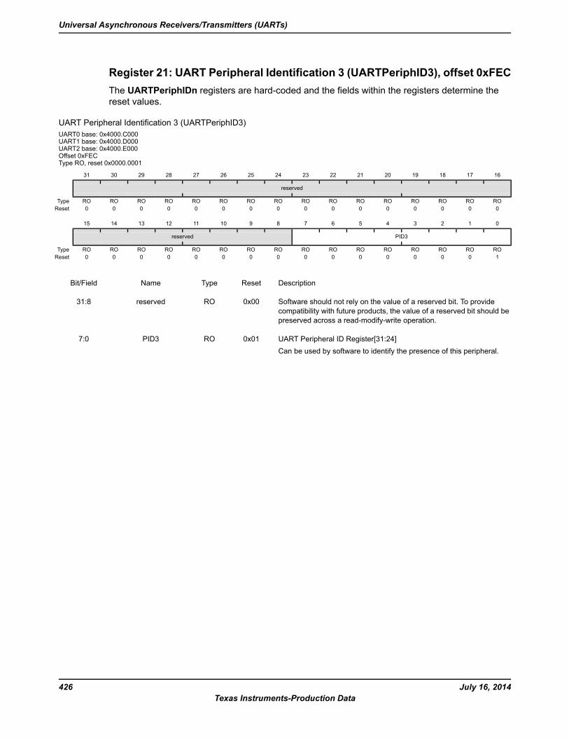
Register 21: UART Peripheral Identification 3 (UARTPeriphID3), offset 0xFECThe UARTPeriphIDn registers are hard-coded and the fields within the registers determine thereset values.
UART Peripheral Identification 3 (UARTPeriphID3)UART0 base: 0x4000.C000UART1 base: 0x4000.D000UART2 base: 0x4000.E000Offset 0xFECType RO, reset 0x0000.0001
16171819202122232425262728293031
reserved
ROROROROROROROROROROROROROROROROType0000000000000000Reset
0123456789101112131415
PID3reserved
ROROROROROROROROROROROROROROROROType1000000000000000Reset
DescriptionResetTypeNameBit/Field
Software should not rely on the value of a reserved bit. To providecompatibility with future products, the value of a reserved bit should bepreserved across a read-modify-write operation.
0x00ROreserved31:8
UART Peripheral ID Register[31:24]Can be used by software to identify the presence of this peripheral.
0x01ROPID37:0
July 16, 2014426Texas Instruments-Production Data
Universal Asynchronous Receivers/Transmitters (UARTs)

Register 22: UART PrimeCell Identification 0 (UARTPCellID0), offset 0xFF0The UARTPCellIDn registers are hard-coded and the fields within the registers determine the resetvalues.
UART PrimeCell Identification 0 (UARTPCellID0)UART0 base: 0x4000.C000UART1 base: 0x4000.D000UART2 base: 0x4000.E000Offset 0xFF0Type RO, reset 0x0000.000D
16171819202122232425262728293031
reserved
ROROROROROROROROROROROROROROROROType0000000000000000Reset
0123456789101112131415
CID0reserved
ROROROROROROROROROROROROROROROROType1011000000000000Reset
DescriptionResetTypeNameBit/Field
Software should not rely on the value of a reserved bit. To providecompatibility with future products, the value of a reserved bit should bepreserved across a read-modify-write operation.
0x00ROreserved31:8
UART PrimeCell ID Register[7:0]Provides software a standard cross-peripheral identification system.
0x0DROCID07:0
427July 16, 2014Texas Instruments-Production Data
Stellaris® LM3S2601 Microcontroller

Register 23: UART PrimeCell Identification 1 (UARTPCellID1), offset 0xFF4The UARTPCellIDn registers are hard-coded and the fields within the registers determine the resetvalues.
UART PrimeCell Identification 1 (UARTPCellID1)UART0 base: 0x4000.C000UART1 base: 0x4000.D000UART2 base: 0x4000.E000Offset 0xFF4Type RO, reset 0x0000.00F0
16171819202122232425262728293031
reserved
ROROROROROROROROROROROROROROROROType0000000000000000Reset
0123456789101112131415
CID1reserved
ROROROROROROROROROROROROROROROROType0000111100000000Reset
DescriptionResetTypeNameBit/Field
Software should not rely on the value of a reserved bit. To providecompatibility with future products, the value of a reserved bit should bepreserved across a read-modify-write operation.
0x00ROreserved31:8
UART PrimeCell ID Register[15:8]Provides software a standard cross-peripheral identification system.
0xF0ROCID17:0
July 16, 2014428Texas Instruments-Production Data
Universal Asynchronous Receivers/Transmitters (UARTs)

Register 24: UART PrimeCell Identification 2 (UARTPCellID2), offset 0xFF8The UARTPCellIDn registers are hard-coded and the fields within the registers determine the resetvalues.
UART PrimeCell Identification 2 (UARTPCellID2)UART0 base: 0x4000.C000UART1 base: 0x4000.D000UART2 base: 0x4000.E000Offset 0xFF8Type RO, reset 0x0000.0005
16171819202122232425262728293031
reserved
ROROROROROROROROROROROROROROROROType0000000000000000Reset
0123456789101112131415
CID2reserved
ROROROROROROROROROROROROROROROROType1010000000000000Reset
DescriptionResetTypeNameBit/Field
Software should not rely on the value of a reserved bit. To providecompatibility with future products, the value of a reserved bit should bepreserved across a read-modify-write operation.
0x00ROreserved31:8
UART PrimeCell ID Register[23:16]Provides software a standard cross-peripheral identification system.
0x05ROCID27:0
429July 16, 2014Texas Instruments-Production Data
Stellaris® LM3S2601 Microcontroller

Register 25: UART PrimeCell Identification 3 (UARTPCellID3), offset 0xFFCThe UARTPCellIDn registers are hard-coded and the fields within the registers determine the resetvalues.
UART PrimeCell Identification 3 (UARTPCellID3)UART0 base: 0x4000.C000UART1 base: 0x4000.D000UART2 base: 0x4000.E000Offset 0xFFCType RO, reset 0x0000.00B1
16171819202122232425262728293031
reserved
ROROROROROROROROROROROROROROROROType0000000000000000Reset
0123456789101112131415
CID3reserved
ROROROROROROROROROROROROROROROROType1000110100000000Reset
DescriptionResetTypeNameBit/Field
Software should not rely on the value of a reserved bit. To providecompatibility with future products, the value of a reserved bit should bepreserved across a read-modify-write operation.
0x00ROreserved31:8
UART PrimeCell ID Register[31:24]Provides software a standard cross-peripheral identification system.
0xB1ROCID37:0
July 16, 2014430Texas Instruments-Production Data
Universal Asynchronous Receivers/Transmitters (UARTs)
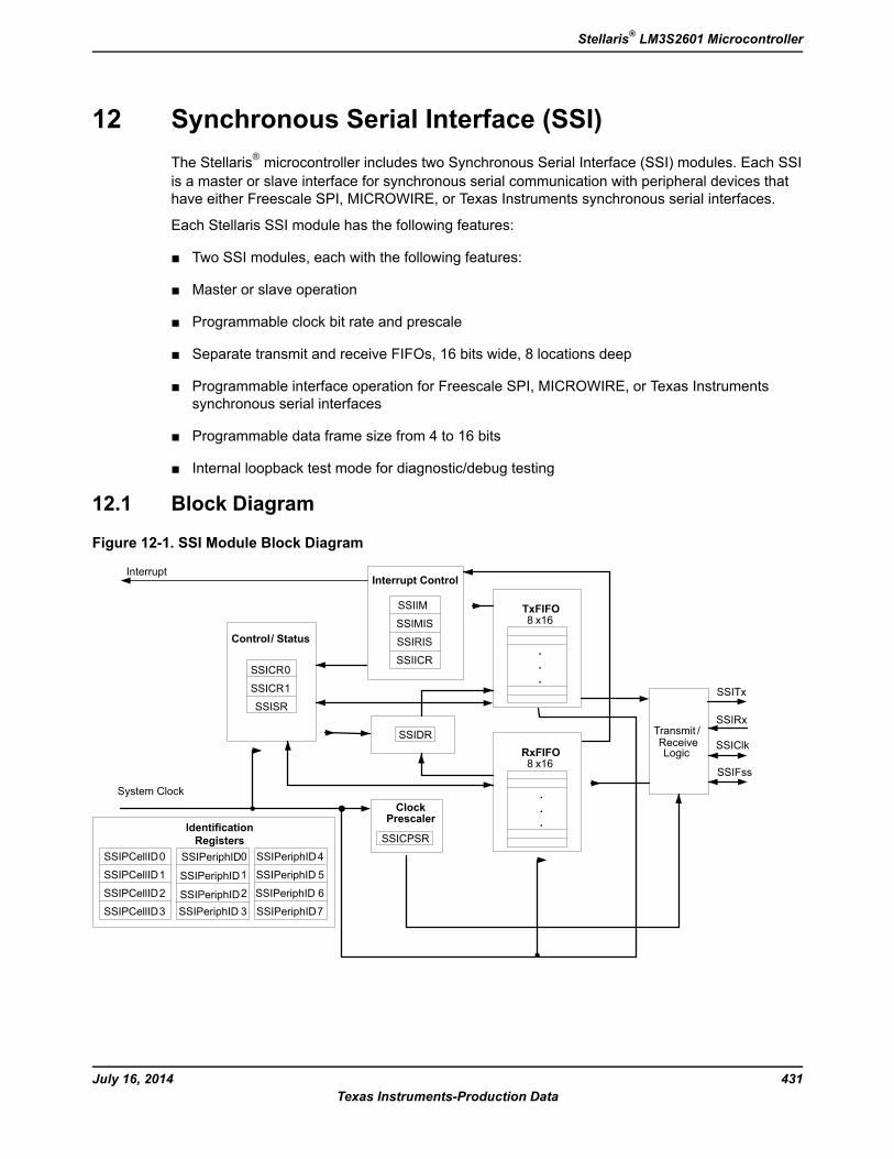
12 Synchronous Serial Interface (SSI)The Stellaris® microcontroller includes two Synchronous Serial Interface (SSI) modules. Each SSIis a master or slave interface for synchronous serial communication with peripheral devices thathave either Freescale SPI, MICROWIRE, or Texas Instruments synchronous serial interfaces.
Each Stellaris SSI module has the following features:
Two SSI modules, each with the following features:
Master or slave operation
Programmable clock bit rate and prescale
Separate transmit and receive FIFOs, 16 bits wide, 8 locations deep
Programmable interface operation for Freescale SPI, MICROWIRE, or Texas Instrumentssynchronous serial interfaces
Programmable data frame size from 4 to 16 bits
Internal loopback test mode for diagnostic/debug testing
12.1 Block Diagram
Figure 12-1. SSI Module Block Diagram
Transmit /ReceiveLogic
ClockPrescaler
SSICPSR
SSICR0
SSICR1
SSISR
Interrupt Control
SSIIM
SSIMIS
SSIRIS
SSIICR
SSIDR
TxFIFO8 x16
.
.
.
RxFIFO8 x16
.
.
.
System Clock
SSITx
SSIRx
SSIClk
SSIFss
Interrupt
IdentificationRegisters
SSIPCellID0 0 SSIPeriphID4
SSIPCellID1 1 SSIPeriphID 5
SSIPCellID2 2 SSIPeriphID 6
SSIPCellID3 SSIPeriphID 3 SSIPeriphID7
Control/ Status
SSIPeriphID
SSIPeriphID
SSIPeriphID
431July 16, 2014Texas Instruments-Production Data
Stellaris® LM3S2601 Microcontroller
12.2 Signal DescriptionTable 12-1 on page 432 and Table 12-2 on page 432 list the external signals of the SSI module anddescribe the function of each. The SSI signals are alternate functions for some GPIO signals anddefault to be GPIO signals at reset., with the exception of the SSI0Clk, SSI0Fss, SSI0Rx, andSSI0Tx pins which default to the SSI function. The column in the table below titled "Pin Assignment"lists the possible GPIO pin placements for the SSI signals. The AFSEL bit in the GPIO AlternateFunction Select (GPIOAFSEL) register (page 302) should be set to choose the SSI function. Formore information on configuring GPIOs, see “General-Purpose Input/Outputs (GPIOs)” on page 279.
Table 12-1. SSI Signals (100LQFP)
DescriptionBuffer TypeaPin TypePin NumberPin Name
SSI module 0 clock.TTLI/O28SSI0Clk
SSI module 0 frame signal.TTLI/O29SSI0Fss
SSI module 0 receive.TTLI30SSI0Rx
SSI module 0 transmit.TTLO31SSI0Tx
SSI module 1 clock.TTLI/O72SSI1Clk
SSI module 1 frame signal.TTLI/O73SSI1Fss
SSI module 1 receive.TTLI74SSI1Rx
SSI module 1 transmit.TTLO75SSI1Tx
a. The TTL designation indicates the pin has TTL-compatible voltage levels.
Table 12-2. SSI Signals (108BGA)
DescriptionBuffer TypeaPin TypePin NumberPin Name
SSI module 0 clock.TTLI/OM4SSI0Clk
SSI module 0 frame signal.TTLI/OL4SSI0Fss
SSI module 0 receive.TTLIL5SSI0Rx
SSI module 0 transmit.TTLOM5SSI0Tx
SSI module 1 clock.TTLI/OA11SSI1Clk
SSI module 1 frame signal.TTLI/OB12SSI1Fss
SSI module 1 receive.TTLIB11SSI1Rx
SSI module 1 transmit.TTLOA12SSI1Tx
a. The TTL designation indicates the pin has TTL-compatible voltage levels.
12.3 Functional DescriptionThe SSI performs serial-to-parallel conversion on data received from a peripheral device. The CPUaccesses data, control, and status information. The transmit and receive paths are buffered withinternal FIFOmemories allowing up to eight 16-bit values to be stored independently in both transmitand receive modes.
12.3.1 Bit Rate GenerationThe SSI includes a programmable bit rate clock divider and prescaler to generate the serial outputclock. Bit rates are supported to 2 MHz and higher, although maximum bit rate is determined byperipheral devices.
The serial bit rate is derived by dividing down the input clock (FSysClk). The clock is first dividedby an even prescale value CPSDVSR from 2 to 254, which is programmed in the SSI Clock Prescale
July 16, 2014432Texas Instruments-Production Data
Synchronous Serial Interface (SSI)
(SSICPSR) register (see page 451). The clock is further divided by a value from 1 to 256, which is1 + SCR, where SCR is the value programmed in the SSI Control0 (SSICR0) register (see page 444).
The frequency of the output clock SSIClk is defined by:
SSIClk = FSysClk / (CPSDVSR * (1 + SCR))
Note: For master mode, the system clock must be at least two times faster than the SSIClk. Forslave mode, the system clock must be at least 12 times faster than the SSIClk.
See “Synchronous Serial Interface (SSI)” on page 604 to view SSI timing parameters.
12.3.2 FIFO Operation
12.3.2.1 Transmit FIFOThe common transmit FIFO is a 16-bit wide, 8-locations deep, first-in, first-out memory buffer. TheCPU writes data to the FIFO by writing the SSI Data (SSIDR) register (see page 448), and data isstored in the FIFO until it is read out by the transmission logic.
When configured as a master or a slave, parallel data is written into the transmit FIFO prior to serialconversion and transmission to the attached slave or master, respectively, through the SSITx pin.
In slave mode, the SSI transmits data each time the master initiates a transaction. If the transmitFIFO is empty and the master initiates, the slave transmits the 8th most recent value in the transmitFIFO. If less than 8 values have been written to the transmit FIFO since the SSI module clock wasenabled using the SSI bit in the RGCG1 register, then 0 is transmitted. Care should be taken toensure that valid data is in the FIFO as needed. The SSI can be configured to generate an interruptwhen the FIFO is empty.
12.3.2.2 Receive FIFOThe common receive FIFO is a 16-bit wide, 8-locations deep, first-in, first-out memory buffer.Received data from the serial interface is stored in the buffer until read out by the CPU, whichaccesses the read FIFO by reading the SSIDR register.
When configured as a master or slave, serial data received through the SSIRx pin is registeredprior to parallel loading into the attached slave or master receive FIFO, respectively.
12.3.3 InterruptsThe SSI can generate interrupts when the following conditions are observed:
Transmit FIFO service
Receive FIFO service
Receive FIFO time-out
Receive FIFO overrun
All of the interrupt events are ORed together before being sent to the interrupt controller, so the SSIcan only generate a single interrupt request to the controller at any given time. You can mask eachof the four individual maskable interrupts by setting the appropriate bits in the SSI Interrupt Mask(SSIIM) register (see page 452). Setting the appropriate mask bit to 1 enables the interrupt.
Provision of the individual outputs, as well as a combined interrupt output, allows use of either aglobal interrupt service routine, or modular device drivers to handle interrupts. The transmit and
433July 16, 2014Texas Instruments-Production Data
Stellaris® LM3S2601 Microcontroller
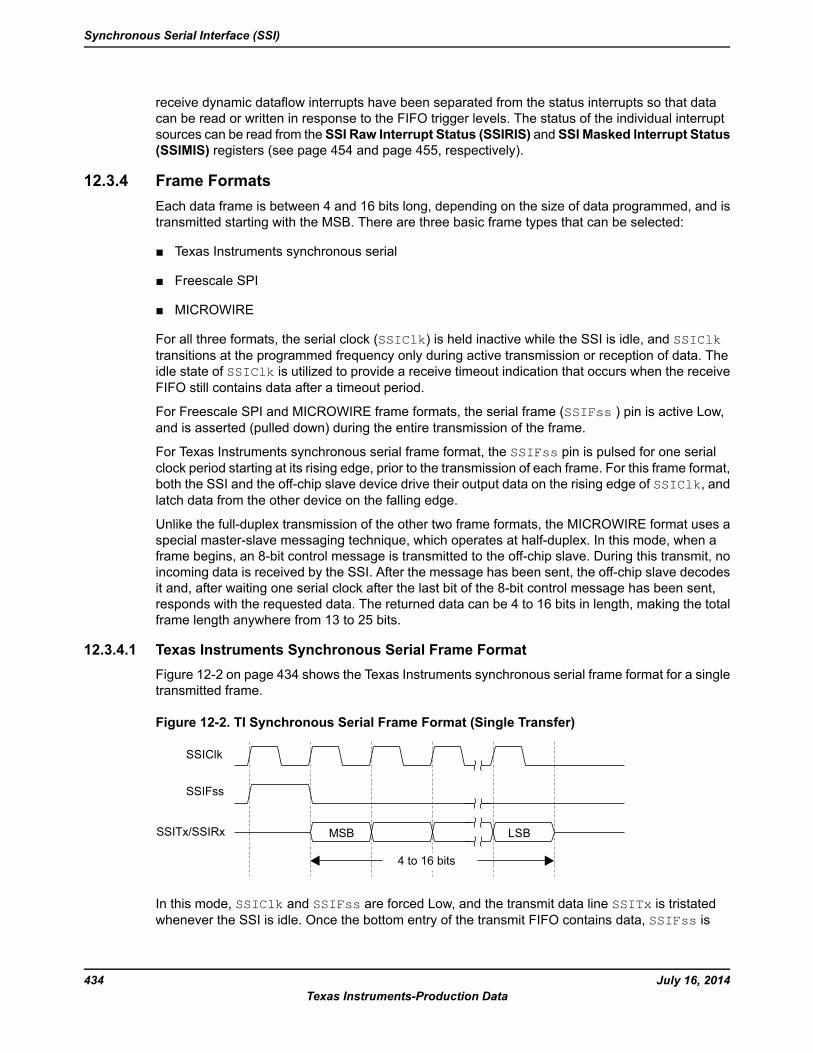
receive dynamic dataflow interrupts have been separated from the status interrupts so that datacan be read or written in response to the FIFO trigger levels. The status of the individual interruptsources can be read from the SSI Raw Interrupt Status (SSIRIS) and SSI Masked Interrupt Status(SSIMIS) registers (see page 454 and page 455, respectively).
12.3.4 Frame FormatsEach data frame is between 4 and 16 bits long, depending on the size of data programmed, and istransmitted starting with the MSB. There are three basic frame types that can be selected:
Texas Instruments synchronous serial
Freescale SPI
MICROWIRE
For all three formats, the serial clock (SSIClk) is held inactive while the SSI is idle, and SSIClktransitions at the programmed frequency only during active transmission or reception of data. Theidle state of SSIClk is utilized to provide a receive timeout indication that occurs when the receiveFIFO still contains data after a timeout period.
For Freescale SPI and MICROWIRE frame formats, the serial frame (SSIFss ) pin is active Low,and is asserted (pulled down) during the entire transmission of the frame.
For Texas Instruments synchronous serial frame format, the SSIFss pin is pulsed for one serialclock period starting at its rising edge, prior to the transmission of each frame. For this frame format,both the SSI and the off-chip slave device drive their output data on the rising edge of SSIClk, andlatch data from the other device on the falling edge.
Unlike the full-duplex transmission of the other two frame formats, the MICROWIRE format uses aspecial master-slave messaging technique, which operates at half-duplex. In this mode, when aframe begins, an 8-bit control message is transmitted to the off-chip slave. During this transmit, noincoming data is received by the SSI. After the message has been sent, the off-chip slave decodesit and, after waiting one serial clock after the last bit of the 8-bit control message has been sent,responds with the requested data. The returned data can be 4 to 16 bits in length, making the totalframe length anywhere from 13 to 25 bits.
12.3.4.1 Texas Instruments Synchronous Serial Frame FormatFigure 12-2 on page 434 shows the Texas Instruments synchronous serial frame format for a singletransmitted frame.
Figure 12-2. TI Synchronous Serial Frame Format (Single Transfer)
SSIClk
SSIFss
SSITx/SSIRx MSB LSB
4 to 16 bits
In this mode, SSIClk and SSIFss are forced Low, and the transmit data line SSITx is tristatedwhenever the SSI is idle. Once the bottom entry of the transmit FIFO contains data, SSIFss is
July 16, 2014434Texas Instruments-Production Data
Synchronous Serial Interface (SSI)
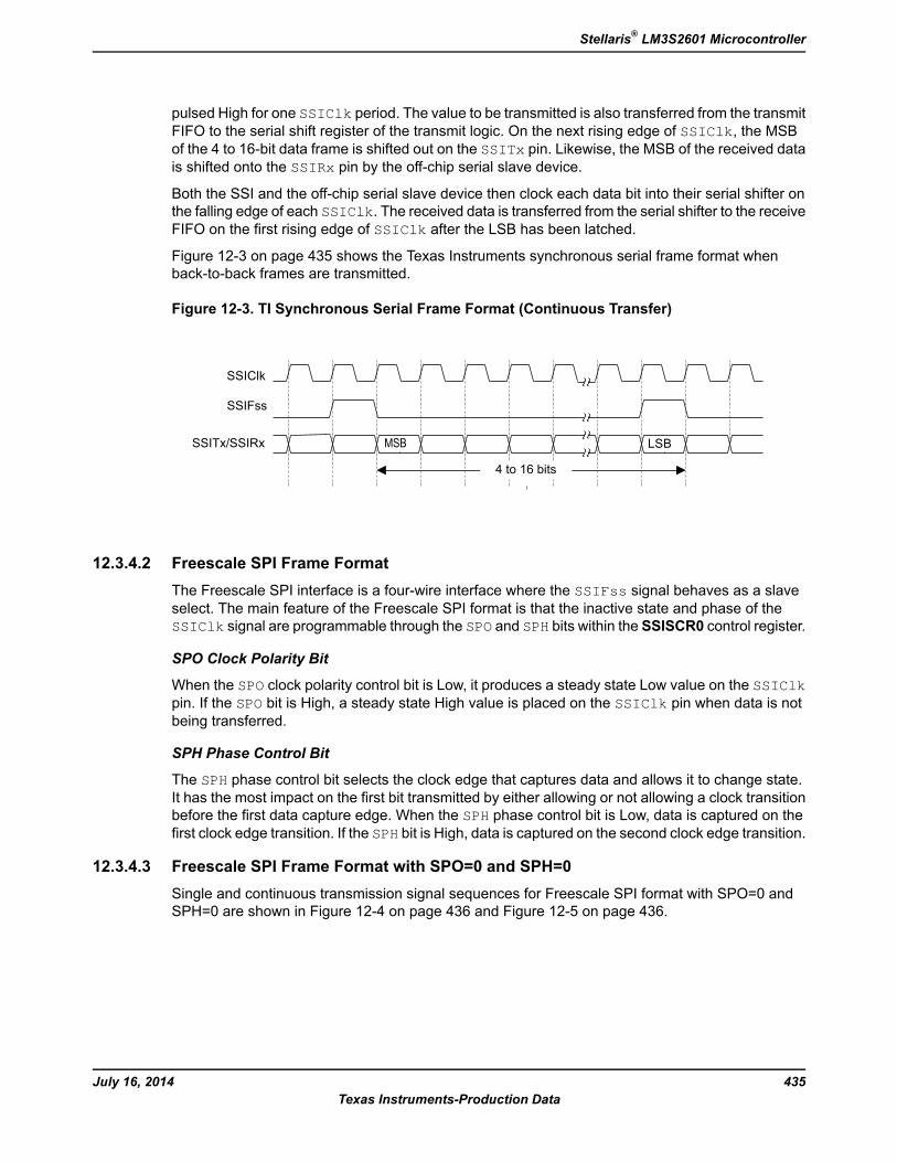
pulsed High for one SSIClk period. The value to be transmitted is also transferred from the transmitFIFO to the serial shift register of the transmit logic. On the next rising edge of SSIClk, the MSBof the 4 to 16-bit data frame is shifted out on the SSITx pin. Likewise, the MSB of the received datais shifted onto the SSIRx pin by the off-chip serial slave device.
Both the SSI and the off-chip serial slave device then clock each data bit into their serial shifter onthe falling edge of each SSIClk. The received data is transferred from the serial shifter to the receiveFIFO on the first rising edge of SSIClk after the LSB has been latched.
Figure 12-3 on page 435 shows the Texas Instruments synchronous serial frame format whenback-to-back frames are transmitted.
Figure 12-3. TI Synchronous Serial Frame Format (Continuous Transfer)
MSB LSB
SSIClk
SSIFss
SSITx/SSIRx
4 to 16 bits
12.3.4.2 Freescale SPI Frame FormatThe Freescale SPI interface is a four-wire interface where the SSIFss signal behaves as a slaveselect. The main feature of the Freescale SPI format is that the inactive state and phase of theSSIClk signal are programmable through the SPO and SPH bits within the SSISCR0 control register.
SPO Clock Polarity Bit
When the SPO clock polarity control bit is Low, it produces a steady state Low value on the SSIClkpin. If the SPO bit is High, a steady state High value is placed on the SSIClk pin when data is notbeing transferred.
SPH Phase Control Bit
The SPH phase control bit selects the clock edge that captures data and allows it to change state.It has the most impact on the first bit transmitted by either allowing or not allowing a clock transitionbefore the first data capture edge. When the SPH phase control bit is Low, data is captured on thefirst clock edge transition. If the SPH bit is High, data is captured on the second clock edge transition.
12.3.4.3 Freescale SPI Frame Format with SPO=0 and SPH=0Single and continuous transmission signal sequences for Freescale SPI format with SPO=0 andSPH=0 are shown in Figure 12-4 on page 436 and Figure 12-5 on page 436.
435July 16, 2014Texas Instruments-Production Data
Stellaris® LM3S2601 Microcontroller
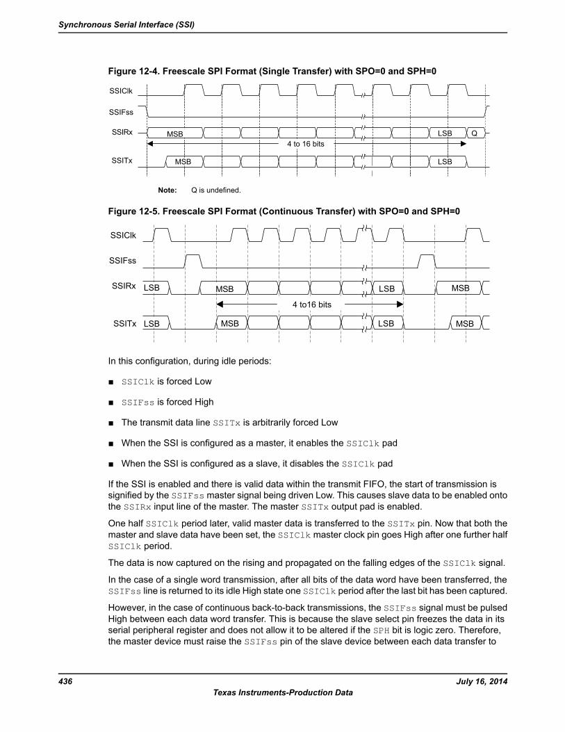
Figure 12-4. Freescale SPI Format (Single Transfer) with SPO=0 and SPH=0
SSIClk
SSIFss
SSIRx Q
SSITx MSB
MSB
LSB
LSB4 to 16 bits
Note: Q is undefined.
Figure 12-5. Freescale SPI Format (Continuous Transfer) with SPO=0 and SPH=0
SSIClk
SSIFss
SSIRx LSB
SSITx MSB LSB
LSB MSB
MSB
MSB
LSB
4 to16 bits
In this configuration, during idle periods:
SSIClk is forced Low
SSIFss is forced High
The transmit data line SSITx is arbitrarily forced Low
When the SSI is configured as a master, it enables the SSIClk pad
When the SSI is configured as a slave, it disables the SSIClk pad
If the SSI is enabled and there is valid data within the transmit FIFO, the start of transmission issignified by the SSIFssmaster signal being driven Low. This causes slave data to be enabled ontothe SSIRx input line of the master. The master SSITx output pad is enabled.
One half SSIClk period later, valid master data is transferred to the SSITx pin. Now that both themaster and slave data have been set, the SSIClkmaster clock pin goes High after one further halfSSIClk period.
The data is now captured on the rising and propagated on the falling edges of the SSIClk signal.
In the case of a single word transmission, after all bits of the data word have been transferred, theSSIFss line is returned to its idle High state one SSIClk period after the last bit has been captured.
However, in the case of continuous back-to-back transmissions, the SSIFss signal must be pulsedHigh between each data word transfer. This is because the slave select pin freezes the data in itsserial peripheral register and does not allow it to be altered if the SPH bit is logic zero. Therefore,the master device must raise the SSIFss pin of the slave device between each data transfer to
July 16, 2014436Texas Instruments-Production Data
Synchronous Serial Interface (SSI)
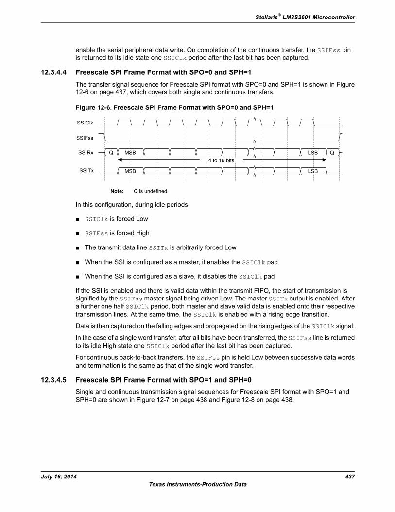
enable the serial peripheral data write. On completion of the continuous transfer, the SSIFss pinis returned to its idle state one SSIClk period after the last bit has been captured.
12.3.4.4 Freescale SPI Frame Format with SPO=0 and SPH=1The transfer signal sequence for Freescale SPI format with SPO=0 and SPH=1 is shown in Figure12-6 on page 437, which covers both single and continuous transfers.
Figure 12-6. Freescale SPI Frame Format with SPO=0 and SPH=1
SSIClk
SSIFss
SSIRx
SSITx
Q
MSB
QMSB
LSB
LSB4 to 16 bits
Q
Note: Q is undefined.
In this configuration, during idle periods:
SSIClk is forced Low
SSIFss is forced High
The transmit data line SSITx is arbitrarily forced Low
When the SSI is configured as a master, it enables the SSIClk pad
When the SSI is configured as a slave, it disables the SSIClk pad
If the SSI is enabled and there is valid data within the transmit FIFO, the start of transmission issignified by the SSIFssmaster signal being driven Low. The master SSITx output is enabled. Aftera further one half SSIClk period, both master and slave valid data is enabled onto their respectivetransmission lines. At the same time, the SSIClk is enabled with a rising edge transition.
Data is then captured on the falling edges and propagated on the rising edges of the SSIClk signal.
In the case of a single word transfer, after all bits have been transferred, the SSIFss line is returnedto its idle High state one SSIClk period after the last bit has been captured.
For continuous back-to-back transfers, the SSIFss pin is held Low between successive data wordsand termination is the same as that of the single word transfer.
12.3.4.5 Freescale SPI Frame Format with SPO=1 and SPH=0Single and continuous transmission signal sequences for Freescale SPI format with SPO=1 andSPH=0 are shown in Figure 12-7 on page 438 and Figure 12-8 on page 438.
437July 16, 2014Texas Instruments-Production Data
Stellaris® LM3S2601 Microcontroller
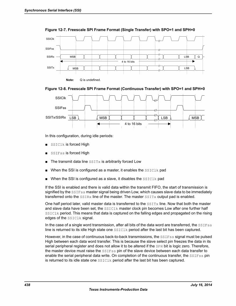
Figure 12-7. Freescale SPI Frame Format (Single Transfer) with SPO=1 and SPH=0
SSIClk
SSIFss
SSIRx
SSITx
QMSB
MSB LSB
LSB
4 to 16 bits
Note: Q is undefined.
Figure 12-8. Freescale SPI Frame Format (Continuous Transfer) with SPO=1 and SPH=0
SSIClk
SSIFss
SSITx/SSIRx MSB LSBLSB MSB
4 to 16 bits
In this configuration, during idle periods:
SSIClk is forced High
SSIFss is forced High
The transmit data line SSITx is arbitrarily forced Low
When the SSI is configured as a master, it enables the SSIClk pad
When the SSI is configured as a slave, it disables the SSIClk pad
If the SSI is enabled and there is valid data within the transmit FIFO, the start of transmission issignified by the SSIFssmaster signal being driven Low, which causes slave data to be immediatelytransferred onto the SSIRx line of the master. The master SSITx output pad is enabled.
One half period later, valid master data is transferred to the SSITx line. Now that both the masterand slave data have been set, the SSIClk master clock pin becomes Low after one further halfSSIClk period. This means that data is captured on the falling edges and propagated on the risingedges of the SSIClk signal.
In the case of a single word transmission, after all bits of the data word are transferred, the SSIFssline is returned to its idle High state one SSIClk period after the last bit has been captured.
However, in the case of continuous back-to-back transmissions, the SSIFss signal must be pulsedHigh between each data word transfer. This is because the slave select pin freezes the data in itsserial peripheral register and does not allow it to be altered if the SPH bit is logic zero. Therefore,the master device must raise the SSIFss pin of the slave device between each data transfer toenable the serial peripheral data write. On completion of the continuous transfer, the SSIFss pinis returned to its idle state one SSIClk period after the last bit has been captured.
July 16, 2014438Texas Instruments-Production Data
Synchronous Serial Interface (SSI)
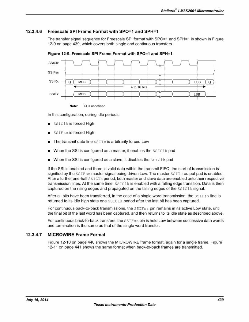
12.3.4.6 Freescale SPI Frame Format with SPO=1 and SPH=1The transfer signal sequence for Freescale SPI format with SPO=1 and SPH=1 is shown in Figure12-9 on page 439, which covers both single and continuous transfers.
Figure 12-9. Freescale SPI Frame Format with SPO=1 and SPH=1
SSIClk
SSIFss
SSIRx
SSITx
Q
MSB
MSB
LSB
LSB4 to 16 bits
Q
Note: Q is undefined.
In this configuration, during idle periods:
SSIClk is forced High
SSIFss is forced High
The transmit data line SSITx is arbitrarily forced Low
When the SSI is configured as a master, it enables the SSIClk pad
When the SSI is configured as a slave, it disables the SSIClk pad
If the SSI is enabled and there is valid data within the transmit FIFO, the start of transmission issignified by the SSIFss master signal being driven Low. The master SSITx output pad is enabled.After a further one-half SSIClk period, both master and slave data are enabled onto their respectivetransmission lines. At the same time, SSIClk is enabled with a falling edge transition. Data is thencaptured on the rising edges and propagated on the falling edges of the SSIClk signal.
After all bits have been transferred, in the case of a single word transmission, the SSIFss line isreturned to its idle high state one SSIClk period after the last bit has been captured.
For continuous back-to-back transmissions, the SSIFss pin remains in its active Low state, untilthe final bit of the last word has been captured, and then returns to its idle state as described above.
For continuous back-to-back transfers, the SSIFss pin is held Low between successive data wordsand termination is the same as that of the single word transfer.
12.3.4.7 MICROWIRE Frame FormatFigure 12-10 on page 440 shows the MICROWIRE frame format, again for a single frame. Figure12-11 on page 441 shows the same format when back-to-back frames are transmitted.
439July 16, 2014Texas Instruments-Production Data
Stellaris® LM3S2601 Microcontroller
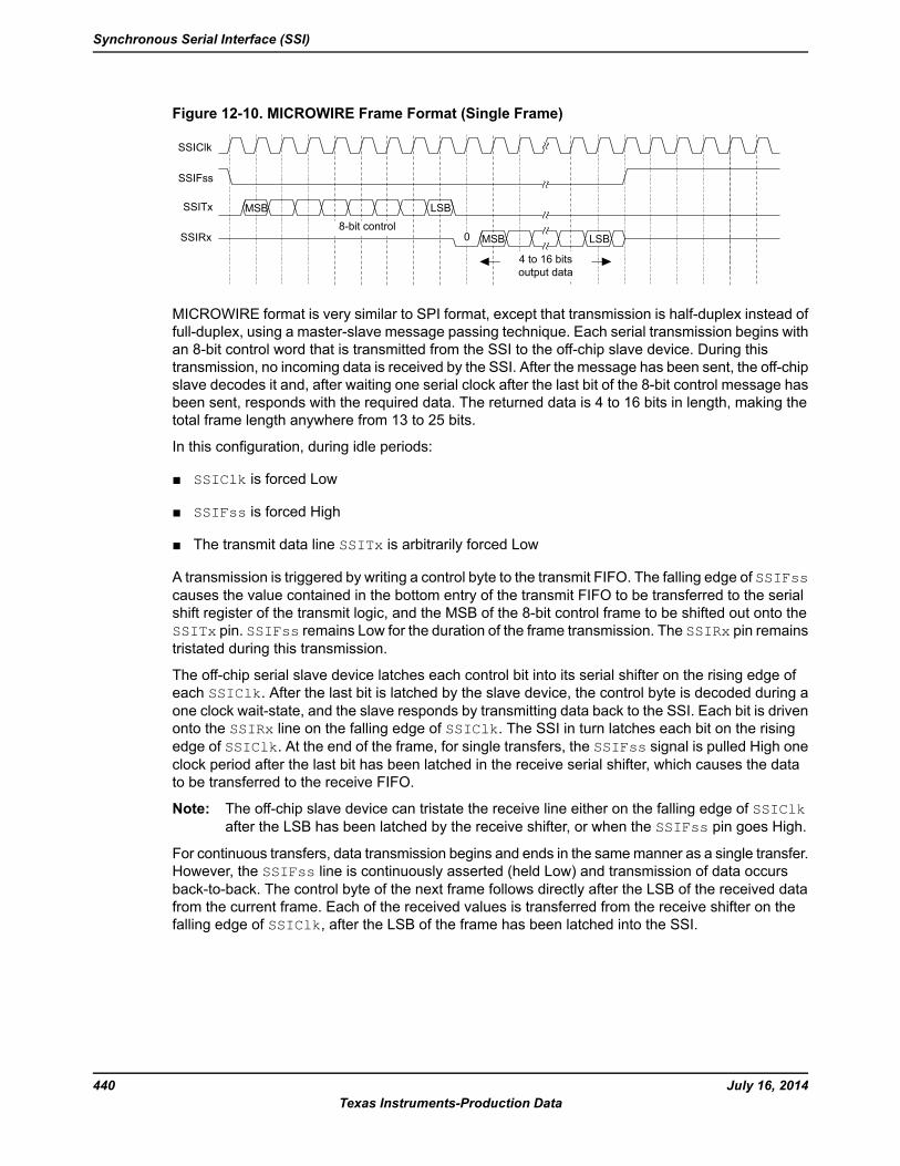
Figure 12-10. MICROWIRE Frame Format (Single Frame)
SSIClk
SSIFss
SSIRx 0
SSITx
8-bit control
4 to 16 bitsoutput data
LSB
MSB
MSB
LSB
MICROWIRE format is very similar to SPI format, except that transmission is half-duplex instead offull-duplex, using a master-slave message passing technique. Each serial transmission begins withan 8-bit control word that is transmitted from the SSI to the off-chip slave device. During thistransmission, no incoming data is received by the SSI. After the message has been sent, the off-chipslave decodes it and, after waiting one serial clock after the last bit of the 8-bit control message hasbeen sent, responds with the required data. The returned data is 4 to 16 bits in length, making thetotal frame length anywhere from 13 to 25 bits.
In this configuration, during idle periods:
SSIClk is forced Low
SSIFss is forced High
The transmit data line SSITx is arbitrarily forced Low
A transmission is triggered by writing a control byte to the transmit FIFO. The falling edge of SSIFsscauses the value contained in the bottom entry of the transmit FIFO to be transferred to the serialshift register of the transmit logic, and the MSB of the 8-bit control frame to be shifted out onto theSSITx pin. SSIFss remains Low for the duration of the frame transmission. The SSIRx pin remainstristated during this transmission.
The off-chip serial slave device latches each control bit into its serial shifter on the rising edge ofeach SSIClk. After the last bit is latched by the slave device, the control byte is decoded during aone clock wait-state, and the slave responds by transmitting data back to the SSI. Each bit is drivenonto the SSIRx line on the falling edge of SSIClk. The SSI in turn latches each bit on the risingedge of SSIClk. At the end of the frame, for single transfers, the SSIFss signal is pulled High oneclock period after the last bit has been latched in the receive serial shifter, which causes the datato be transferred to the receive FIFO.
Note: The off-chip slave device can tristate the receive line either on the falling edge of SSIClkafter the LSB has been latched by the receive shifter, or when the SSIFss pin goes High.
For continuous transfers, data transmission begins and ends in the samemanner as a single transfer.However, the SSIFss line is continuously asserted (held Low) and transmission of data occursback-to-back. The control byte of the next frame follows directly after the LSB of the received datafrom the current frame. Each of the received values is transferred from the receive shifter on thefalling edge of SSIClk, after the LSB of the frame has been latched into the SSI.
July 16, 2014440Texas Instruments-Production Data
Synchronous Serial Interface (SSI)
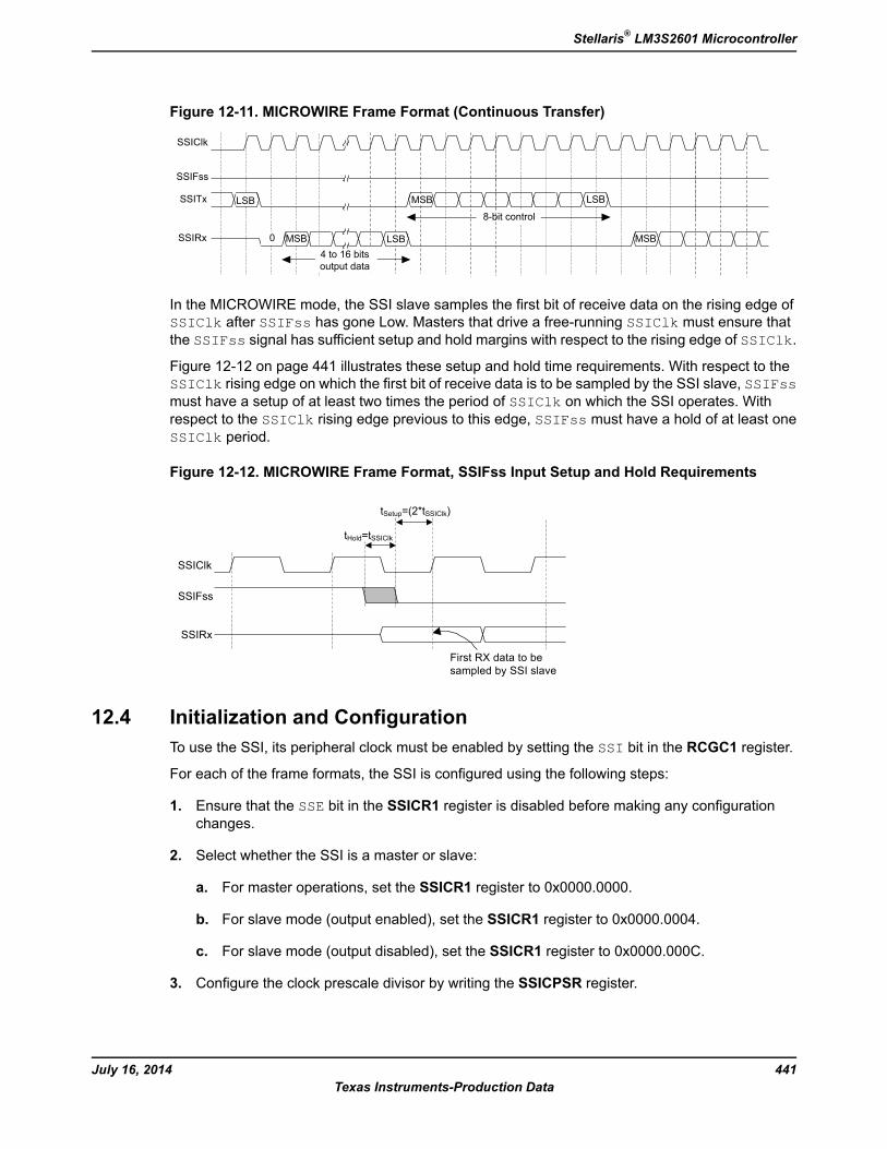
Figure 12-11. MICROWIRE Frame Format (Continuous Transfer)
SSIClk
SSIFss
LSBMSBSSIRx 0
SSITx LSBLSB
MSB4 to 16 bitsoutput data
8-bit control
MSB
In the MICROWIRE mode, the SSI slave samples the first bit of receive data on the rising edge ofSSIClk after SSIFss has gone Low. Masters that drive a free-running SSIClk must ensure thatthe SSIFss signal has sufficient setup and hold margins with respect to the rising edge of SSIClk.
Figure 12-12 on page 441 illustrates these setup and hold time requirements. With respect to theSSIClk rising edge on which the first bit of receive data is to be sampled by the SSI slave, SSIFssmust have a setup of at least two times the period of SSIClk on which the SSI operates. Withrespect to the SSIClk rising edge previous to this edge, SSIFss must have a hold of at least oneSSIClk period.
Figure 12-12. MICROWIRE Frame Format, SSIFss Input Setup and Hold Requirements
SSIClk
SSIFss
SSIRx
First RX data to besampled by SSI slave
tHold=tSSIClk
tSetup=(2*tSSIClk)
12.4 Initialization and ConfigurationTo use the SSI, its peripheral clock must be enabled by setting the SSI bit in the RCGC1 register.
For each of the frame formats, the SSI is configured using the following steps:
1. Ensure that the SSE bit in the SSICR1 register is disabled before making any configurationchanges.
2. Select whether the SSI is a master or slave:
a. For master operations, set the SSICR1 register to 0x0000.0000.
b. For slave mode (output enabled), set the SSICR1 register to 0x0000.0004.
c. For slave mode (output disabled), set the SSICR1 register to 0x0000.000C.
3. Configure the clock prescale divisor by writing the SSICPSR register.
441July 16, 2014Texas Instruments-Production Data
Stellaris® LM3S2601 Microcontroller
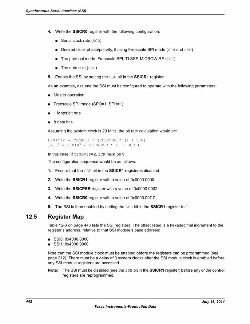
4. Write the SSICR0 register with the following configuration:
Serial clock rate (SCR)
Desired clock phase/polarity, if using Freescale SPI mode (SPH and SPO)
The protocol mode: Freescale SPI, TI SSF, MICROWIRE (FRF)
The data size (DSS)
5. Enable the SSI by setting the SSE bit in the SSICR1 register.
As an example, assume the SSI must be configured to operate with the following parameters:
Master operation
Freescale SPI mode (SPO=1, SPH=1)
1 Mbps bit rate
8 data bits
Assuming the system clock is 20 MHz, the bit rate calculation would be:
FSSIClk = FSysClk / (CPSDVSR * (1 + SCR))1x106 = 20x106 / (CPSDVSR * (1 + SCR))
In this case, if CPSDVSR=2, SCR must be 9.
The configuration sequence would be as follows:
1. Ensure that the SSE bit in the SSICR1 register is disabled.
2. Write the SSICR1 register with a value of 0x0000.0000.
3. Write the SSICPSR register with a value of 0x0000.0002.
4. Write the SSICR0 register with a value of 0x0000.09C7.
5. The SSI is then enabled by setting the SSE bit in the SSICR1 register to 1.
12.5 Register MapTable 12-3 on page 443 lists the SSI registers. The offset listed is a hexadecimal increment to theregister’s address, relative to that SSI module’s base address:
SSI0: 0x4000.8000 SSI1: 0x4000.9000
Note that the SSI module clock must be enabled before the registers can be programmed (seepage 212). There must be a delay of 3 system clocks after the SSI module clock is enabled beforeany SSI module registers are accessed.
Note: The SSI must be disabled (see the SSE bit in the SSICR1 register) before any of the controlregisters are reprogrammed.
July 16, 2014442Texas Instruments-Production Data
Synchronous Serial Interface (SSI)
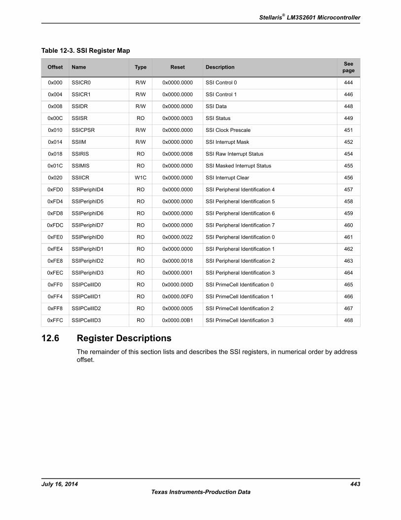
Table 12-3. SSI Register Map
SeepageDescriptionResetTypeNameOffset
444SSI Control 00x0000.0000R/WSSICR00x000
446SSI Control 10x0000.0000R/WSSICR10x004
448SSI Data0x0000.0000R/WSSIDR0x008
449SSI Status0x0000.0003ROSSISR0x00C
451SSI Clock Prescale0x0000.0000R/WSSICPSR0x010
452SSI Interrupt Mask0x0000.0000R/WSSIIM0x014
454SSI Raw Interrupt Status0x0000.0008ROSSIRIS0x018
455SSI Masked Interrupt Status0x0000.0000ROSSIMIS0x01C
456SSI Interrupt Clear0x0000.0000W1CSSIICR0x020
457SSI Peripheral Identification 40x0000.0000ROSSIPeriphID40xFD0
458SSI Peripheral Identification 50x0000.0000ROSSIPeriphID50xFD4
459SSI Peripheral Identification 60x0000.0000ROSSIPeriphID60xFD8
460SSI Peripheral Identification 70x0000.0000ROSSIPeriphID70xFDC
461SSI Peripheral Identification 00x0000.0022ROSSIPeriphID00xFE0
462SSI Peripheral Identification 10x0000.0000ROSSIPeriphID10xFE4
463SSI Peripheral Identification 20x0000.0018ROSSIPeriphID20xFE8
464SSI Peripheral Identification 30x0000.0001ROSSIPeriphID30xFEC
465SSI PrimeCell Identification 00x0000.000DROSSIPCellID00xFF0
466SSI PrimeCell Identification 10x0000.00F0ROSSIPCellID10xFF4
467SSI PrimeCell Identification 20x0000.0005ROSSIPCellID20xFF8
468SSI PrimeCell Identification 30x0000.00B1ROSSIPCellID30xFFC
12.6 Register DescriptionsThe remainder of this section lists and describes the SSI registers, in numerical order by addressoffset.
443July 16, 2014Texas Instruments-Production Data
Stellaris® LM3S2601 Microcontroller
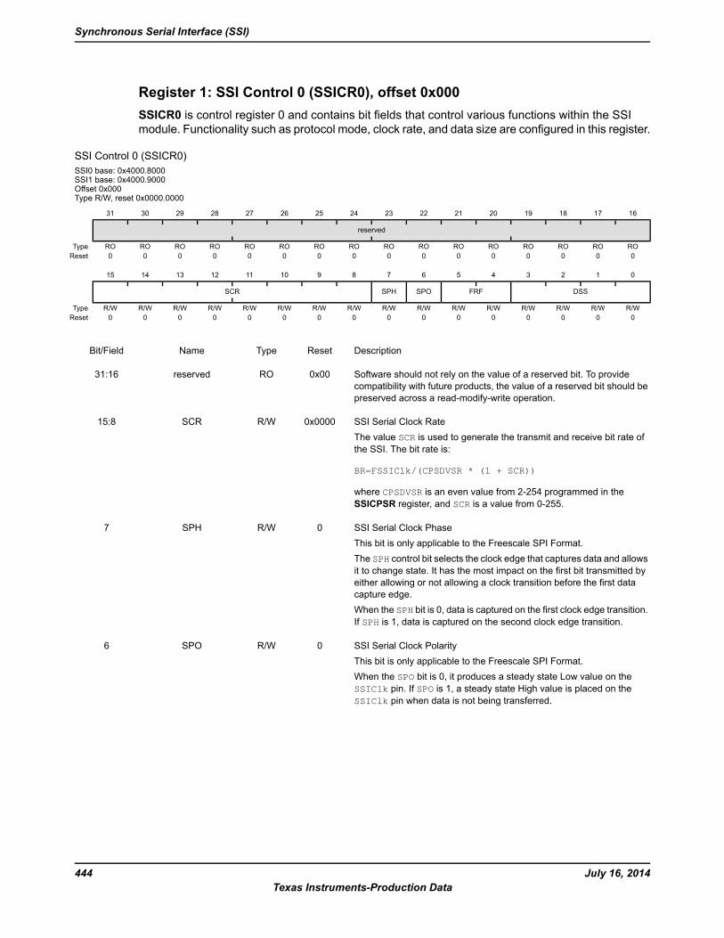
Register 1: SSI Control 0 (SSICR0), offset 0x000SSICR0 is control register 0 and contains bit fields that control various functions within the SSImodule. Functionality such as protocol mode, clock rate, and data size are configured in this register.
SSI Control 0 (SSICR0)SSI0 base: 0x4000.8000SSI1 base: 0x4000.9000Offset 0x000Type R/W, reset 0x0000.0000
16171819202122232425262728293031
reserved
ROROROROROROROROROROROROROROROROType0000000000000000Reset
0123456789101112131415
DSSFRFSPOSPHSCR
R/WR/WR/WR/WR/WR/WR/WR/WR/WR/WR/WR/WR/WR/WR/WR/WType0000000000000000Reset
DescriptionResetTypeNameBit/Field
Software should not rely on the value of a reserved bit. To providecompatibility with future products, the value of a reserved bit should bepreserved across a read-modify-write operation.
0x00ROreserved31:16
SSI Serial Clock RateThe value SCR is used to generate the transmit and receive bit rate ofthe SSI. The bit rate is:
BR=FSSIClk/(CPSDVSR * (1 + SCR))
where CPSDVSR is an even value from 2-254 programmed in theSSICPSR register, and SCR is a value from 0-255.
0x0000R/WSCR15:8
SSI Serial Clock PhaseThis bit is only applicable to the Freescale SPI Format.The SPH control bit selects the clock edge that captures data and allowsit to change state. It has the most impact on the first bit transmitted byeither allowing or not allowing a clock transition before the first datacapture edge.When the SPH bit is 0, data is captured on the first clock edge transition.If SPH is 1, data is captured on the second clock edge transition.
0R/WSPH7
SSI Serial Clock PolarityThis bit is only applicable to the Freescale SPI Format.When the SPO bit is 0, it produces a steady state Low value on theSSIClk pin. If SPO is 1, a steady state High value is placed on theSSIClk pin when data is not being transferred.
0R/WSPO6
July 16, 2014444Texas Instruments-Production Data
Synchronous Serial Interface (SSI)
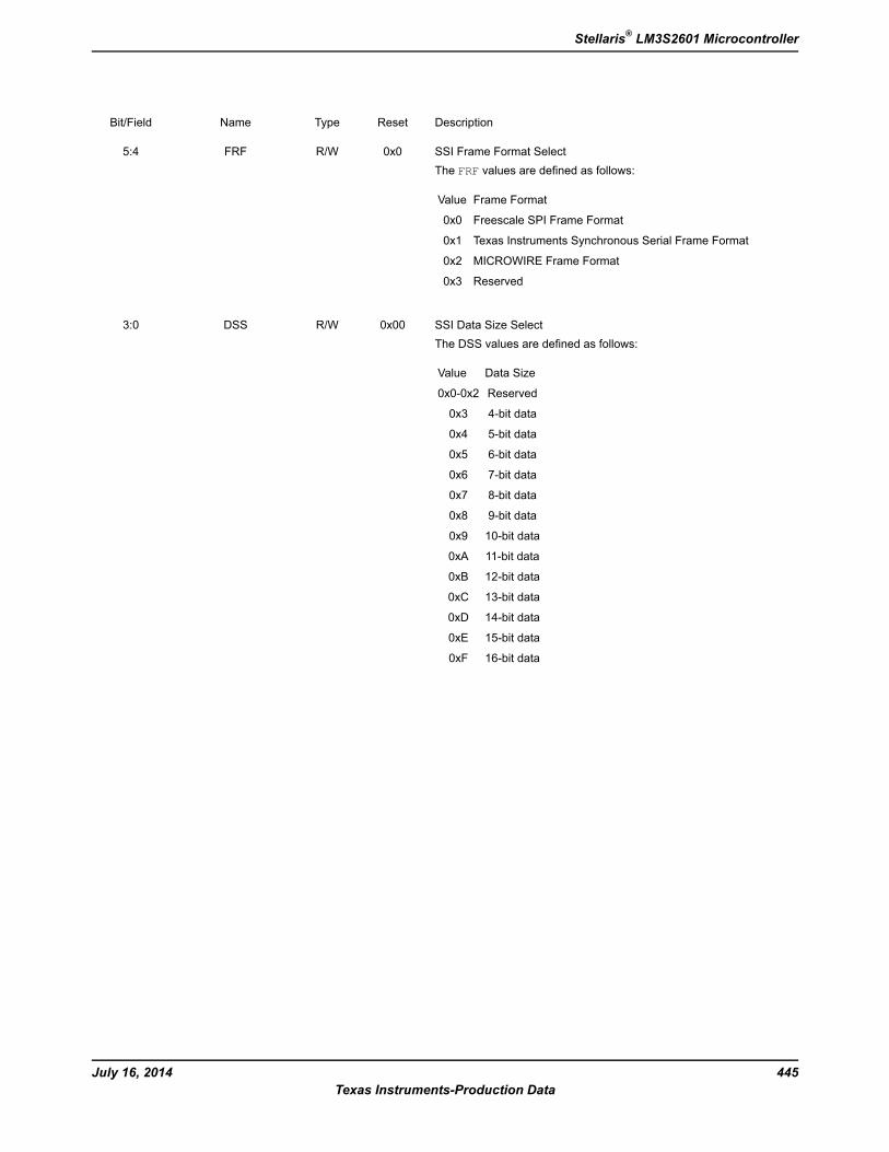
DescriptionResetTypeNameBit/Field
SSI Frame Format SelectThe FRF values are defined as follows:
Frame FormatValue
Freescale SPI Frame Format0x0
Texas Instruments Synchronous Serial Frame Format0x1
MICROWIRE Frame Format0x2
Reserved0x3
0x0R/WFRF5:4
SSI Data Size SelectThe DSS values are defined as follows:
Data SizeValue
Reserved0x0-0x2
4-bit data0x3
5-bit data0x4
6-bit data0x5
7-bit data0x6
8-bit data0x7
9-bit data0x8
10-bit data0x9
11-bit data0xA
12-bit data0xB
13-bit data0xC
14-bit data0xD
15-bit data0xE
16-bit data0xF
0x00R/WDSS3:0
445July 16, 2014Texas Instruments-Production Data
Stellaris® LM3S2601 Microcontroller
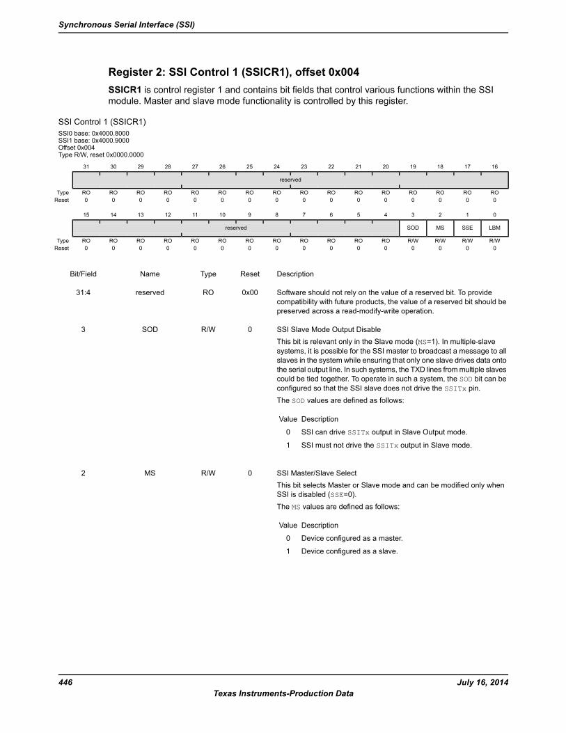
Register 2: SSI Control 1 (SSICR1), offset 0x004SSICR1 is control register 1 and contains bit fields that control various functions within the SSImodule. Master and slave mode functionality is controlled by this register.
SSI Control 1 (SSICR1)SSI0 base: 0x4000.8000SSI1 base: 0x4000.9000Offset 0x004Type R/W, reset 0x0000.0000
16171819202122232425262728293031
reserved
ROROROROROROROROROROROROROROROROType0000000000000000Reset
0123456789101112131415
LBMSSEMSSODreserved
R/WR/WR/WR/WROROROROROROROROROROROROType0000000000000000Reset
DescriptionResetTypeNameBit/Field
Software should not rely on the value of a reserved bit. To providecompatibility with future products, the value of a reserved bit should bepreserved across a read-modify-write operation.
0x00ROreserved31:4
SSI Slave Mode Output DisableThis bit is relevant only in the Slave mode (MS=1). In multiple-slavesystems, it is possible for the SSI master to broadcast a message to allslaves in the system while ensuring that only one slave drives data ontothe serial output line. In such systems, the TXD lines frommultiple slavescould be tied together. To operate in such a system, the SOD bit can beconfigured so that the SSI slave does not drive the SSITx pin.The SOD values are defined as follows:
DescriptionValue
SSI can drive SSITx output in Slave Output mode.0
SSI must not drive the SSITx output in Slave mode.1
0R/WSOD3
SSI Master/Slave SelectThis bit selects Master or Slave mode and can be modified only whenSSI is disabled (SSE=0).The MS values are defined as follows:
DescriptionValue
Device configured as a master.0
Device configured as a slave.1
0R/WMS2
July 16, 2014446Texas Instruments-Production Data
Synchronous Serial Interface (SSI)
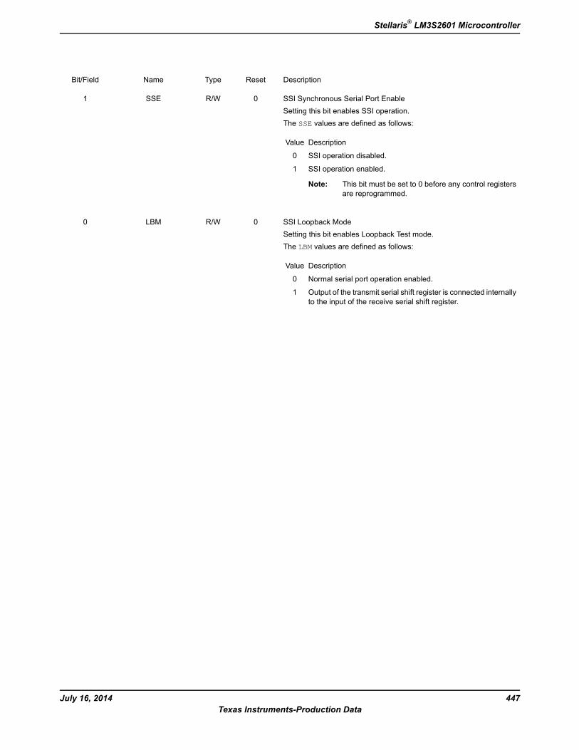
DescriptionResetTypeNameBit/Field
SSI Synchronous Serial Port EnableSetting this bit enables SSI operation.The SSE values are defined as follows:
DescriptionValue
SSI operation disabled.0
SSI operation enabled.1
Note: This bit must be set to 0 before any control registersare reprogrammed.
0R/WSSE1
SSI Loopback ModeSetting this bit enables Loopback Test mode.The LBM values are defined as follows:
DescriptionValue
Normal serial port operation enabled.0
Output of the transmit serial shift register is connected internallyto the input of the receive serial shift register.
1
0R/WLBM0
447July 16, 2014Texas Instruments-Production Data
Stellaris® LM3S2601 Microcontroller
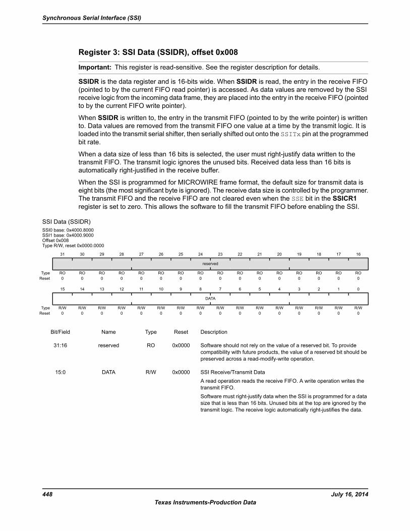
Register 3: SSI Data (SSIDR), offset 0x008
Important: This register is read-sensitive. See the register description for details.
SSIDR is the data register and is 16-bits wide. When SSIDR is read, the entry in the receive FIFO(pointed to by the current FIFO read pointer) is accessed. As data values are removed by the SSIreceive logic from the incoming data frame, they are placed into the entry in the receive FIFO (pointedto by the current FIFO write pointer).
When SSIDR is written to, the entry in the transmit FIFO (pointed to by the write pointer) is writtento. Data values are removed from the transmit FIFO one value at a time by the transmit logic. It isloaded into the transmit serial shifter, then serially shifted out onto the SSITx pin at the programmedbit rate.
When a data size of less than 16 bits is selected, the user must right-justify data written to thetransmit FIFO. The transmit logic ignores the unused bits. Received data less than 16 bits isautomatically right-justified in the receive buffer.
When the SSI is programmed for MICROWIRE frame format, the default size for transmit data iseight bits (the most significant byte is ignored). The receive data size is controlled by the programmer.The transmit FIFO and the receive FIFO are not cleared even when the SSE bit in the SSICR1register is set to zero. This allows the software to fill the transmit FIFO before enabling the SSI.
SSI Data (SSIDR)SSI0 base: 0x4000.8000SSI1 base: 0x4000.9000Offset 0x008Type R/W, reset 0x0000.0000
16171819202122232425262728293031
reserved
ROROROROROROROROROROROROROROROROType0000000000000000Reset
0123456789101112131415
DATA
R/WR/WR/WR/WR/WR/WR/WR/WR/WR/WR/WR/WR/WR/WR/WR/WType0000000000000000Reset
DescriptionResetTypeNameBit/Field
Software should not rely on the value of a reserved bit. To providecompatibility with future products, the value of a reserved bit should bepreserved across a read-modify-write operation.
0x0000ROreserved31:16
SSI Receive/Transmit DataA read operation reads the receive FIFO. A write operation writes thetransmit FIFO.Software must right-justify data when the SSI is programmed for a datasize that is less than 16 bits. Unused bits at the top are ignored by thetransmit logic. The receive logic automatically right-justifies the data.
0x0000R/WDATA15:0
July 16, 2014448Texas Instruments-Production Data
Synchronous Serial Interface (SSI)
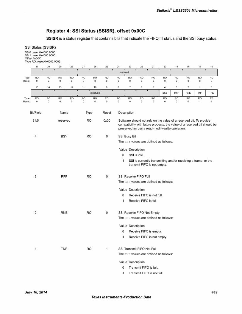
Register 4: SSI Status (SSISR), offset 0x00CSSISR is a status register that contains bits that indicate the FIFO fill status and the SSI busy status.
SSI Status (SSISR)SSI0 base: 0x4000.8000SSI1 base: 0x4000.9000Offset 0x00CType RO, reset 0x0000.0003
16171819202122232425262728293031
reserved
ROROROROROROROROROROROROROROROROType0000000000000000Reset
0123456789101112131415
TFETNFRNERFFBSYreserved
R0ROROROROROROROROROROROROROROROType1100000000000000Reset
DescriptionResetTypeNameBit/Field
Software should not rely on the value of a reserved bit. To providecompatibility with future products, the value of a reserved bit should bepreserved across a read-modify-write operation.
0x00ROreserved31:5
SSI Busy BitThe BSY values are defined as follows:
DescriptionValue
SSI is idle.0
SSI is currently transmitting and/or receiving a frame, or thetransmit FIFO is not empty.
1
0ROBSY4
SSI Receive FIFO FullThe RFF values are defined as follows:
DescriptionValue
Receive FIFO is not full.0
Receive FIFO is full.1
0RORFF3
SSI Receive FIFO Not EmptyThe RNE values are defined as follows:
DescriptionValue
Receive FIFO is empty.0
Receive FIFO is not empty.1
0RORNE2
SSI Transmit FIFO Not FullThe TNF values are defined as follows:
DescriptionValue
Transmit FIFO is full.0
Transmit FIFO is not full.1
1ROTNF1
449July 16, 2014Texas Instruments-Production Data
Stellaris® LM3S2601 Microcontroller

DescriptionResetTypeNameBit/Field
SSI Transmit FIFO EmptyThe TFE values are defined as follows:
DescriptionValue
Transmit FIFO is not empty.0
Transmit FIFO is empty.1
1R0TFE0
July 16, 2014450Texas Instruments-Production Data
Synchronous Serial Interface (SSI)
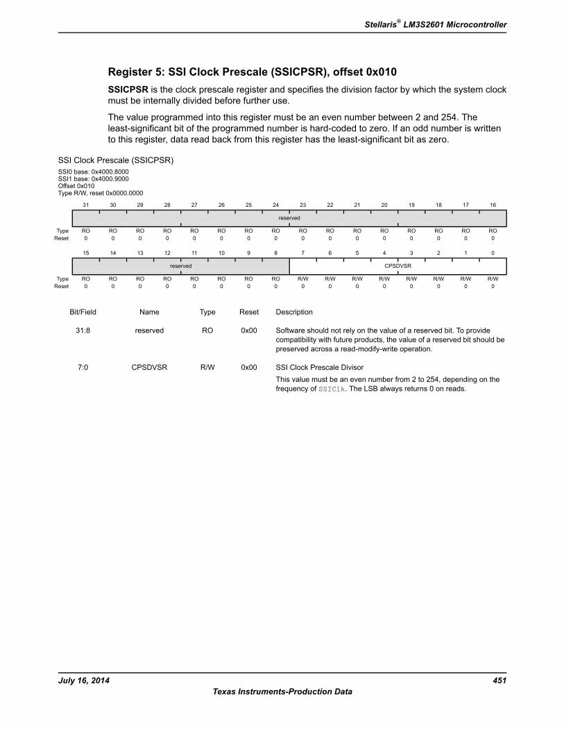
Register 5: SSI Clock Prescale (SSICPSR), offset 0x010SSICPSR is the clock prescale register and specifies the division factor by which the system clockmust be internally divided before further use.
The value programmed into this register must be an even number between 2 and 254. Theleast-significant bit of the programmed number is hard-coded to zero. If an odd number is writtento this register, data read back from this register has the least-significant bit as zero.
SSI Clock Prescale (SSICPSR)SSI0 base: 0x4000.8000SSI1 base: 0x4000.9000Offset 0x010Type R/W, reset 0x0000.0000
16171819202122232425262728293031
reserved
ROROROROROROROROROROROROROROROROType0000000000000000Reset
0123456789101112131415
CPSDVSRreserved
R/WR/WR/WR/WR/WR/WR/WR/WROROROROROROROROType0000000000000000Reset
DescriptionResetTypeNameBit/Field
Software should not rely on the value of a reserved bit. To providecompatibility with future products, the value of a reserved bit should bepreserved across a read-modify-write operation.
0x00ROreserved31:8
SSI Clock Prescale DivisorThis value must be an even number from 2 to 254, depending on thefrequency of SSIClk. The LSB always returns 0 on reads.
0x00R/WCPSDVSR7:0
451July 16, 2014Texas Instruments-Production Data
Stellaris® LM3S2601 Microcontroller
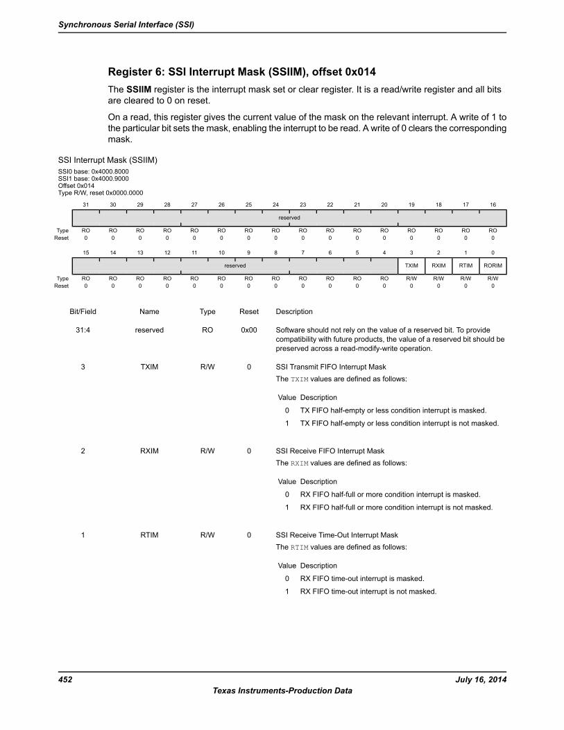
Register 6: SSI Interrupt Mask (SSIIM), offset 0x014The SSIIM register is the interrupt mask set or clear register. It is a read/write register and all bitsare cleared to 0 on reset.
On a read, this register gives the current value of the mask on the relevant interrupt. A write of 1 tothe particular bit sets the mask, enabling the interrupt to be read. A write of 0 clears the correspondingmask.
SSI Interrupt Mask (SSIIM)SSI0 base: 0x4000.8000SSI1 base: 0x4000.9000Offset 0x014Type R/W, reset 0x0000.0000
16171819202122232425262728293031
reserved
ROROROROROROROROROROROROROROROROType0000000000000000Reset
0123456789101112131415
RORIMRTIMRXIMTXIMreserved
R/WR/WR/WR/WROROROROROROROROROROROROType0000000000000000Reset
DescriptionResetTypeNameBit/Field
Software should not rely on the value of a reserved bit. To providecompatibility with future products, the value of a reserved bit should bepreserved across a read-modify-write operation.
0x00ROreserved31:4
SSI Transmit FIFO Interrupt MaskThe TXIM values are defined as follows:
DescriptionValue
TX FIFO half-empty or less condition interrupt is masked.0
TX FIFO half-empty or less condition interrupt is not masked.1
0R/WTXIM3
SSI Receive FIFO Interrupt MaskThe RXIM values are defined as follows:
DescriptionValue
RX FIFO half-full or more condition interrupt is masked.0
RX FIFO half-full or more condition interrupt is not masked.1
0R/WRXIM2
SSI Receive Time-Out Interrupt MaskThe RTIM values are defined as follows:
DescriptionValue
RX FIFO time-out interrupt is masked.0
RX FIFO time-out interrupt is not masked.1
0R/WRTIM1
July 16, 2014452Texas Instruments-Production Data
Synchronous Serial Interface (SSI)

DescriptionResetTypeNameBit/Field
SSI Receive Overrun Interrupt MaskThe RORIM values are defined as follows:
DescriptionValue
RX FIFO overrun interrupt is masked.0
RX FIFO overrun interrupt is not masked.1
0R/WRORIM0
453July 16, 2014Texas Instruments-Production Data
Stellaris® LM3S2601 Microcontroller
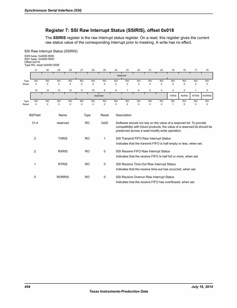
Register 7: SSI Raw Interrupt Status (SSIRIS), offset 0x018The SSIRIS register is the raw interrupt status register. On a read, this register gives the currentraw status value of the corresponding interrupt prior to masking. A write has no effect.
SSI Raw Interrupt Status (SSIRIS)SSI0 base: 0x4000.8000SSI1 base: 0x4000.9000Offset 0x018Type RO, reset 0x0000.0008
16171819202122232425262728293031
reserved
ROROROROROROROROROROROROROROROROType0000000000000000Reset
0123456789101112131415
RORRISRTRISRXRISTXRISreserved
ROROROROROROROROROROROROROROROROType0001000000000000Reset
DescriptionResetTypeNameBit/Field
Software should not rely on the value of a reserved bit. To providecompatibility with future products, the value of a reserved bit should bepreserved across a read-modify-write operation.
0x00ROreserved31:4
SSI Transmit FIFO Raw Interrupt StatusIndicates that the transmit FIFO is half empty or less, when set.
1ROTXRIS3
SSI Receive FIFO Raw Interrupt StatusIndicates that the receive FIFO is half full or more, when set.
0RORXRIS2
SSI Receive Time-Out Raw Interrupt StatusIndicates that the receive time-out has occurred, when set.
0RORTRIS1
SSI Receive Overrun Raw Interrupt StatusIndicates that the receive FIFO has overflowed, when set.
0RORORRIS0
July 16, 2014454Texas Instruments-Production Data
Synchronous Serial Interface (SSI)
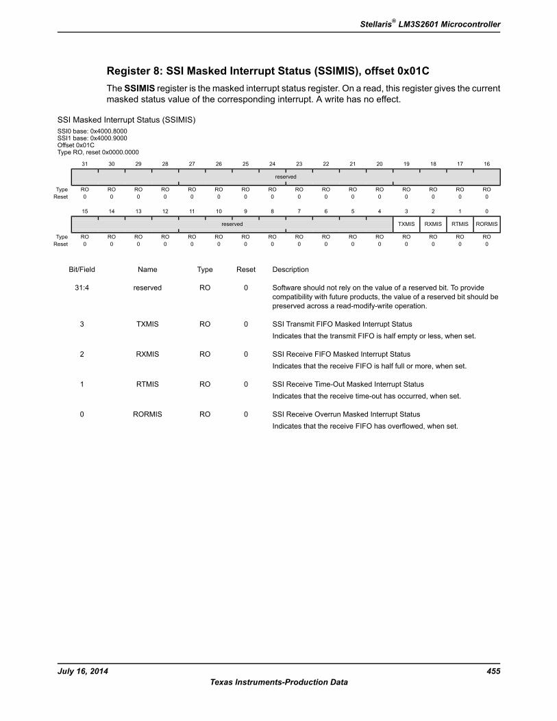
Register 8: SSI Masked Interrupt Status (SSIMIS), offset 0x01CThe SSIMIS register is the masked interrupt status register. On a read, this register gives the currentmasked status value of the corresponding interrupt. A write has no effect.
SSI Masked Interrupt Status (SSIMIS)SSI0 base: 0x4000.8000SSI1 base: 0x4000.9000Offset 0x01CType RO, reset 0x0000.0000
16171819202122232425262728293031
reserved
ROROROROROROROROROROROROROROROROType0000000000000000Reset
0123456789101112131415
RORMISRTMISRXMISTXMISreserved
ROROROROROROROROROROROROROROROROType0000000000000000Reset
DescriptionResetTypeNameBit/Field
Software should not rely on the value of a reserved bit. To providecompatibility with future products, the value of a reserved bit should bepreserved across a read-modify-write operation.
0ROreserved31:4
SSI Transmit FIFO Masked Interrupt StatusIndicates that the transmit FIFO is half empty or less, when set.
0ROTXMIS3
SSI Receive FIFO Masked Interrupt StatusIndicates that the receive FIFO is half full or more, when set.
0RORXMIS2
SSI Receive Time-Out Masked Interrupt StatusIndicates that the receive time-out has occurred, when set.
0RORTMIS1
SSI Receive Overrun Masked Interrupt StatusIndicates that the receive FIFO has overflowed, when set.
0RORORMIS0
455July 16, 2014Texas Instruments-Production Data
Stellaris® LM3S2601 Microcontroller
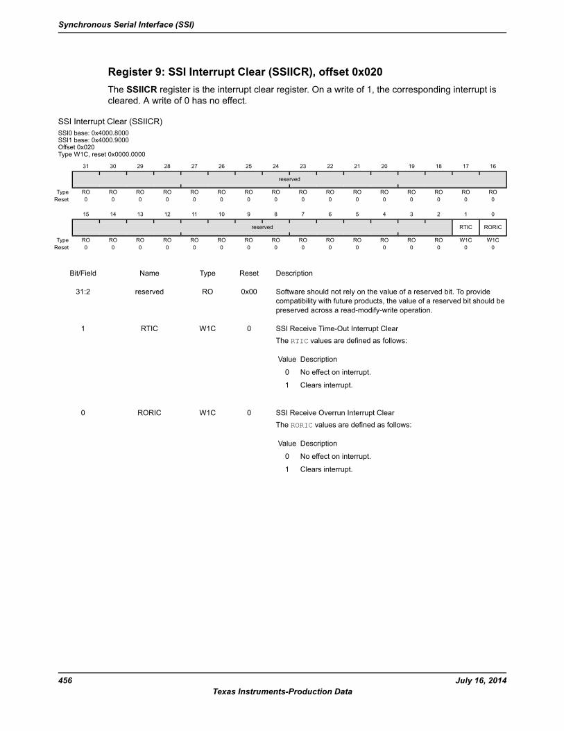
Register 9: SSI Interrupt Clear (SSIICR), offset 0x020The SSIICR register is the interrupt clear register. On a write of 1, the corresponding interrupt iscleared. A write of 0 has no effect.
SSI Interrupt Clear (SSIICR)SSI0 base: 0x4000.8000SSI1 base: 0x4000.9000Offset 0x020Type W1C, reset 0x0000.0000
16171819202122232425262728293031
reserved
ROROROROROROROROROROROROROROROROType0000000000000000Reset
0123456789101112131415
RORICRTICreserved
W1CW1CROROROROROROROROROROROROROROType0000000000000000Reset
DescriptionResetTypeNameBit/Field
Software should not rely on the value of a reserved bit. To providecompatibility with future products, the value of a reserved bit should bepreserved across a read-modify-write operation.
0x00ROreserved31:2
SSI Receive Time-Out Interrupt ClearThe RTIC values are defined as follows:
DescriptionValue
No effect on interrupt.0
Clears interrupt.1
0W1CRTIC1
SSI Receive Overrun Interrupt ClearThe RORIC values are defined as follows:
DescriptionValue
No effect on interrupt.0
Clears interrupt.1
0W1CRORIC0
July 16, 2014456Texas Instruments-Production Data
Synchronous Serial Interface (SSI)
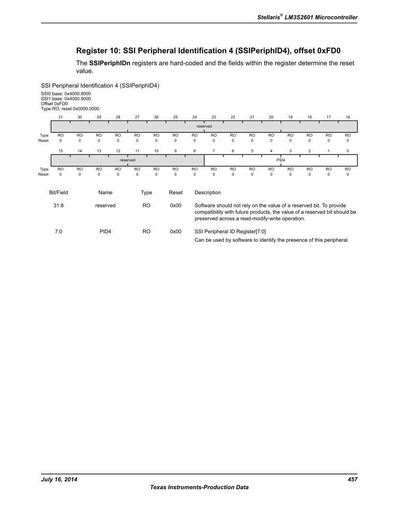
Register 10: SSI Peripheral Identification 4 (SSIPeriphID4), offset 0xFD0The SSIPeriphIDn registers are hard-coded and the fields within the register determine the resetvalue.
SSI Peripheral Identification 4 (SSIPeriphID4)SSI0 base: 0x4000.8000SSI1 base: 0x4000.9000Offset 0xFD0Type RO, reset 0x0000.0000
16171819202122232425262728293031
reserved
ROROROROROROROROROROROROROROROROType0000000000000000Reset
0123456789101112131415
PID4reserved
ROROROROROROROROROROROROROROROROType0000000000000000Reset
DescriptionResetTypeNameBit/Field
Software should not rely on the value of a reserved bit. To providecompatibility with future products, the value of a reserved bit should bepreserved across a read-modify-write operation.
0x00ROreserved31:8
SSI Peripheral ID Register[7:0]Can be used by software to identify the presence of this peripheral.
0x00ROPID47:0
457July 16, 2014Texas Instruments-Production Data
Stellaris® LM3S2601 Microcontroller

Register 11: SSI Peripheral Identification 5 (SSIPeriphID5), offset 0xFD4The SSIPeriphIDn registers are hard-coded and the fields within the register determine the resetvalue.
SSI Peripheral Identification 5 (SSIPeriphID5)SSI0 base: 0x4000.8000SSI1 base: 0x4000.9000Offset 0xFD4Type RO, reset 0x0000.0000
16171819202122232425262728293031
reserved
ROROROROROROROROROROROROROROROROType0000000000000000Reset
0123456789101112131415
PID5reserved
ROROROROROROROROROROROROROROROROType0000000000000000Reset
DescriptionResetTypeNameBit/Field
Software should not rely on the value of a reserved bit. To providecompatibility with future products, the value of a reserved bit should bepreserved across a read-modify-write operation.
0x00ROreserved31:8
SSI Peripheral ID Register[15:8]Can be used by software to identify the presence of this peripheral.
0x00ROPID57:0
July 16, 2014458Texas Instruments-Production Data
Synchronous Serial Interface (SSI)
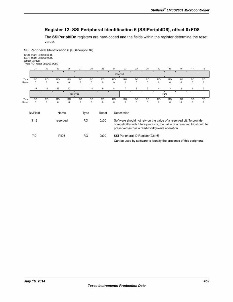
Register 12: SSI Peripheral Identification 6 (SSIPeriphID6), offset 0xFD8The SSIPeriphIDn registers are hard-coded and the fields within the register determine the resetvalue.
SSI Peripheral Identification 6 (SSIPeriphID6)SSI0 base: 0x4000.8000SSI1 base: 0x4000.9000Offset 0xFD8Type RO, reset 0x0000.0000
16171819202122232425262728293031
reserved
ROROROROROROROROROROROROROROROROType0000000000000000Reset
0123456789101112131415
PID6reserved
ROROROROROROROROROROROROROROROROType0000000000000000Reset
DescriptionResetTypeNameBit/Field
Software should not rely on the value of a reserved bit. To providecompatibility with future products, the value of a reserved bit should bepreserved across a read-modify-write operation.
0x00ROreserved31:8
SSI Peripheral ID Register[23:16]Can be used by software to identify the presence of this peripheral.
0x00ROPID67:0
459July 16, 2014Texas Instruments-Production Data
Stellaris® LM3S2601 Microcontroller

Register 13: SSI Peripheral Identification 7 (SSIPeriphID7), offset 0xFDCThe SSIPeriphIDn registers are hard-coded and the fields within the register determine the resetvalue.
SSI Peripheral Identification 7 (SSIPeriphID7)SSI0 base: 0x4000.8000SSI1 base: 0x4000.9000Offset 0xFDCType RO, reset 0x0000.0000
16171819202122232425262728293031
reserved
ROROROROROROROROROROROROROROROROType0000000000000000Reset
0123456789101112131415
PID7reserved
ROROROROROROROROROROROROROROROROType0000000000000000Reset
DescriptionResetTypeNameBit/Field
Software should not rely on the value of a reserved bit. To providecompatibility with future products, the value of a reserved bit should bepreserved across a read-modify-write operation.
0x00ROreserved31:8
SSI Peripheral ID Register[31:24]Can be used by software to identify the presence of this peripheral.
0x00ROPID77:0
July 16, 2014460Texas Instruments-Production Data
Synchronous Serial Interface (SSI)

Register 14: SSI Peripheral Identification 0 (SSIPeriphID0), offset 0xFE0The SSIPeriphIDn registers are hard-coded and the fields within the register determine the resetvalue.
SSI Peripheral Identification 0 (SSIPeriphID0)SSI0 base: 0x4000.8000SSI1 base: 0x4000.9000Offset 0xFE0Type RO, reset 0x0000.0022
16171819202122232425262728293031
reserved
ROROROROROROROROROROROROROROROROType0000000000000000Reset
0123456789101112131415
PID0reserved
ROROROROROROROROROROROROROROROROType0100010000000000Reset
DescriptionResetTypeNameBit/Field
Software should not rely on the value of a reserved bit. To providecompatibility with future products, the value of a reserved bit should bepreserved across a read-modify-write operation.
0ROreserved31:8
SSI Peripheral ID Register[7:0]Can be used by software to identify the presence of this peripheral.
0x22ROPID07:0
461July 16, 2014Texas Instruments-Production Data
Stellaris® LM3S2601 Microcontroller
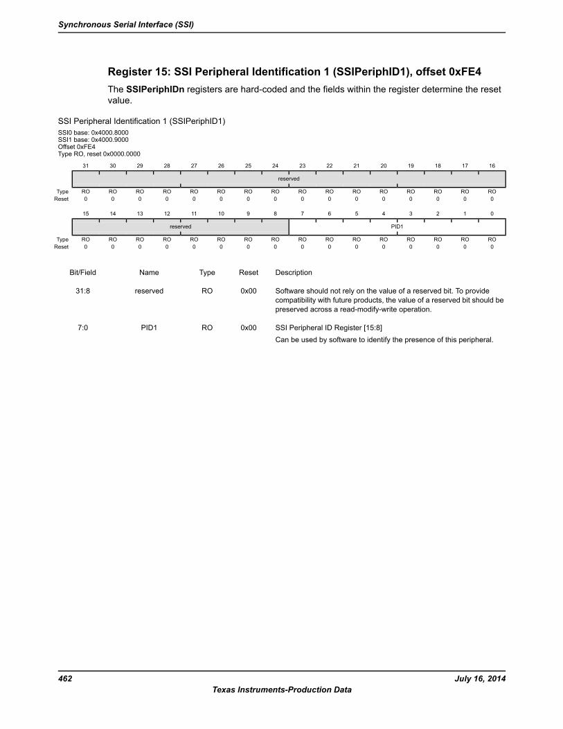
Register 15: SSI Peripheral Identification 1 (SSIPeriphID1), offset 0xFE4The SSIPeriphIDn registers are hard-coded and the fields within the register determine the resetvalue.
SSI Peripheral Identification 1 (SSIPeriphID1)SSI0 base: 0x4000.8000SSI1 base: 0x4000.9000Offset 0xFE4Type RO, reset 0x0000.0000
16171819202122232425262728293031
reserved
ROROROROROROROROROROROROROROROROType0000000000000000Reset
0123456789101112131415
PID1reserved
ROROROROROROROROROROROROROROROROType0000000000000000Reset
DescriptionResetTypeNameBit/Field
Software should not rely on the value of a reserved bit. To providecompatibility with future products, the value of a reserved bit should bepreserved across a read-modify-write operation.
0x00ROreserved31:8
SSI Peripheral ID Register [15:8]Can be used by software to identify the presence of this peripheral.
0x00ROPID17:0
July 16, 2014462Texas Instruments-Production Data
Synchronous Serial Interface (SSI)

Register 16: SSI Peripheral Identification 2 (SSIPeriphID2), offset 0xFE8The SSIPeriphIDn registers are hard-coded and the fields within the register determine the resetvalue.
SSI Peripheral Identification 2 (SSIPeriphID2)SSI0 base: 0x4000.8000SSI1 base: 0x4000.9000Offset 0xFE8Type RO, reset 0x0000.0018
16171819202122232425262728293031
reserved
ROROROROROROROROROROROROROROROROType0000000000000000Reset
0123456789101112131415
PID2reserved
ROROROROROROROROROROROROROROROROType0001100000000000Reset
DescriptionResetTypeNameBit/Field
Software should not rely on the value of a reserved bit. To providecompatibility with future products, the value of a reserved bit should bepreserved across a read-modify-write operation.
0x00ROreserved31:8
SSI Peripheral ID Register [23:16]Can be used by software to identify the presence of this peripheral.
0x18ROPID27:0
463July 16, 2014Texas Instruments-Production Data
Stellaris® LM3S2601 Microcontroller
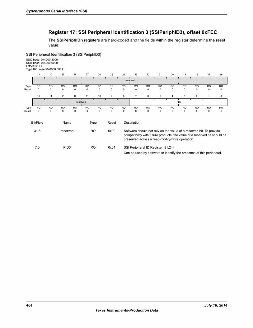
Register 17: SSI Peripheral Identification 3 (SSIPeriphID3), offset 0xFECThe SSIPeriphIDn registers are hard-coded and the fields within the register determine the resetvalue.
SSI Peripheral Identification 3 (SSIPeriphID3)SSI0 base: 0x4000.8000SSI1 base: 0x4000.9000Offset 0xFECType RO, reset 0x0000.0001
16171819202122232425262728293031
reserved
ROROROROROROROROROROROROROROROROType0000000000000000Reset
0123456789101112131415
PID3reserved
ROROROROROROROROROROROROROROROROType1000000000000000Reset
DescriptionResetTypeNameBit/Field
Software should not rely on the value of a reserved bit. To providecompatibility with future products, the value of a reserved bit should bepreserved across a read-modify-write operation.
0x00ROreserved31:8
SSI Peripheral ID Register [31:24]Can be used by software to identify the presence of this peripheral.
0x01ROPID37:0
July 16, 2014464Texas Instruments-Production Data
Synchronous Serial Interface (SSI)
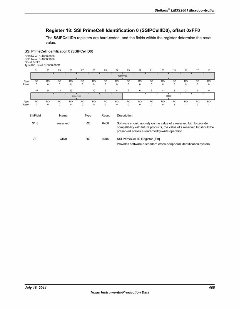
Register 18: SSI PrimeCell Identification 0 (SSIPCellID0), offset 0xFF0The SSIPCellIDn registers are hard-coded, and the fields within the register determine the resetvalue.
SSI PrimeCell Identification 0 (SSIPCellID0)SSI0 base: 0x4000.8000SSI1 base: 0x4000.9000Offset 0xFF0Type RO, reset 0x0000.000D
16171819202122232425262728293031
reserved
ROROROROROROROROROROROROROROROROType0000000000000000Reset
0123456789101112131415
CID0reserved
ROROROROROROROROROROROROROROROROType1011000000000000Reset
DescriptionResetTypeNameBit/Field
Software should not rely on the value of a reserved bit. To providecompatibility with future products, the value of a reserved bit should bepreserved across a read-modify-write operation.
0x00ROreserved31:8
SSI PrimeCell ID Register [7:0]Provides software a standard cross-peripheral identification system.
0x0DROCID07:0
465July 16, 2014Texas Instruments-Production Data
Stellaris® LM3S2601 Microcontroller
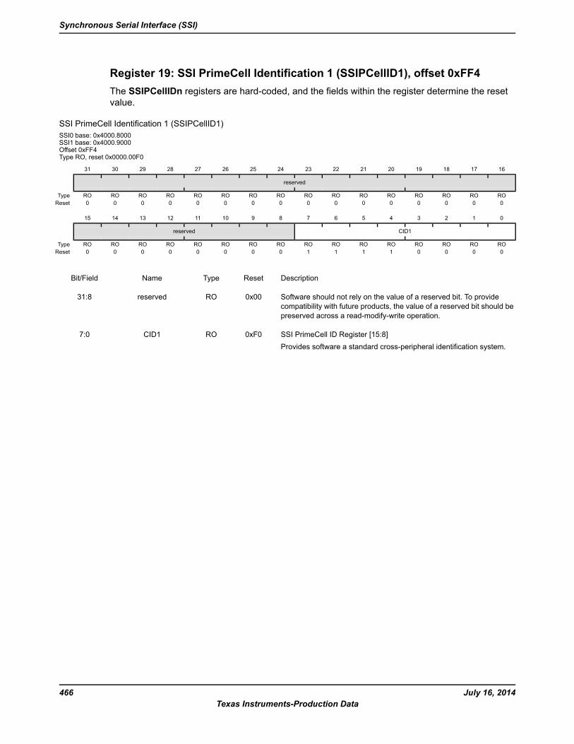
Register 19: SSI PrimeCell Identification 1 (SSIPCellID1), offset 0xFF4The SSIPCellIDn registers are hard-coded, and the fields within the register determine the resetvalue.
SSI PrimeCell Identification 1 (SSIPCellID1)SSI0 base: 0x4000.8000SSI1 base: 0x4000.9000Offset 0xFF4Type RO, reset 0x0000.00F0
16171819202122232425262728293031
reserved
ROROROROROROROROROROROROROROROROType0000000000000000Reset
0123456789101112131415
CID1reserved
ROROROROROROROROROROROROROROROROType0000111100000000Reset
DescriptionResetTypeNameBit/Field
Software should not rely on the value of a reserved bit. To providecompatibility with future products, the value of a reserved bit should bepreserved across a read-modify-write operation.
0x00ROreserved31:8
SSI PrimeCell ID Register [15:8]Provides software a standard cross-peripheral identification system.
0xF0ROCID17:0
July 16, 2014466Texas Instruments-Production Data
Synchronous Serial Interface (SSI)

Register 20: SSI PrimeCell Identification 2 (SSIPCellID2), offset 0xFF8The SSIPCellIDn registers are hard-coded, and the fields within the register determine the resetvalue.
SSI PrimeCell Identification 2 (SSIPCellID2)SSI0 base: 0x4000.8000SSI1 base: 0x4000.9000Offset 0xFF8Type RO, reset 0x0000.0005
16171819202122232425262728293031
reserved
ROROROROROROROROROROROROROROROROType0000000000000000Reset
0123456789101112131415
CID2reserved
ROROROROROROROROROROROROROROROROType1010000000000000Reset
DescriptionResetTypeNameBit/Field
Software should not rely on the value of a reserved bit. To providecompatibility with future products, the value of a reserved bit should bepreserved across a read-modify-write operation.
0x00ROreserved31:8
SSI PrimeCell ID Register [23:16]Provides software a standard cross-peripheral identification system.
0x05ROCID27:0
467July 16, 2014Texas Instruments-Production Data
Stellaris® LM3S2601 Microcontroller

Register 21: SSI PrimeCell Identification 3 (SSIPCellID3), offset 0xFFCThe SSIPCellIDn registers are hard-coded, and the fields within the register determine the resetvalue.
SSI PrimeCell Identification 3 (SSIPCellID3)SSI0 base: 0x4000.8000SSI1 base: 0x4000.9000Offset 0xFFCType RO, reset 0x0000.00B1
16171819202122232425262728293031
reserved
ROROROROROROROROROROROROROROROROType0000000000000000Reset
0123456789101112131415
CID3reserved
ROROROROROROROROROROROROROROROROType1000110100000000Reset
DescriptionResetTypeNameBit/Field
Software should not rely on the value of a reserved bit. To providecompatibility with future products, the value of a reserved bit should bepreserved across a read-modify-write operation.
0x00ROreserved31:8
SSI PrimeCell ID Register [31:24]Provides software a standard cross-peripheral identification system.
0xB1ROCID37:0
July 16, 2014468Texas Instruments-Production Data
Synchronous Serial Interface (SSI)
13 Inter-Integrated Circuit (I2C) InterfaceThe Inter-Integrated Circuit (I2C) bus provides bi-directional data transfer through a two-wire design(a serial data line SDA and a serial clock line SCL), and interfaces to external I2C devices such asserial memory (RAMs and ROMs), networking devices, LCDs, tone generators, and so on. The I2Cbus may also be used for system testing and diagnostic purposes in product development andmanufacture. The LM3S2601 microcontroller includes two I2C modules, providing the ability tointeract (both send and receive) with other I2C devices on the bus.
The Stellaris® I2C interface has the following features:
Two I2C modules, each with the following features:
Devices on the I2C bus can be designated as either a master or a slave
– Supports both sending and receiving data as either a master or a slave
– Supports simultaneous master and slave operation
Four I2C modes
– Master transmit
– Master receive
– Slave transmit
– Slave receive
Two transmission speeds: Standard (100 Kbps) and Fast (400 Kbps)
Master and slave interrupt generation
– Master generates interrupts when a transmit or receive operation completes (or aborts dueto an error)
– Slave generates interrupts when data has been sent or requested by a master
Master with arbitration and clock synchronization, multimaster support, and 7-bit addressingmode
469July 16, 2014Texas Instruments-Production Data
Stellaris® LM3S2601 Microcontroller
13.1 Block Diagram
Figure 13-1. I2C Block Diagram
I2C I/O Select
I2C Master Core
Interrupt
I2C Slave Core
I2CSCL
I2CSDA
I2CSDA
I2CSCL
I2CSDA
I2CSCL
I2CMSA
I2CMCS
I2CMDR
I2CMTPR
I2CMIMR
I2CMRIS
I2CMICR
I2CMCR
I2CSOAR
I2CSCSR
I2CSDR
I2CSIM
I2CSRIS
I2CSMIS
I2CSICRI2CMMIS
I2C Control
13.2 Signal DescriptionTable 13-1 on page 470 and Table 13-2 on page 470 list the external signals of the I2C interface anddescribe the function of each. The I2C interface signals are alternate functions for some GPIO signalsand default to be GPIO signals at reset., with the exception of the I2C0SCL and I2CSDA pins whichdefault to the I2C function. The column in the table below titled "Pin Assignment" lists the possibleGPIO pin placements for the I2C signals. The AFSEL bit in the GPIO Alternate Function Select(GPIOAFSEL) register (page 302) should be set to choose the I2C function. Note that the I2C pinsshould be set to open drain using the GPIO Open Drain Select (GPIOODR) register. For moreinformation on configuring GPIOs, see “General-Purpose Input/Outputs (GPIOs)” on page 279.
Table 13-1. I2C Signals (100LQFP)
DescriptionBuffer TypeaPin TypePin NumberPin Name
I2C module 0 clock.ODI/O70I2C0SCL
I2C module 0 data.ODI/O71I2C0SDA
I2C module 1 clock.ODI/O34I2C1SCL
I2C module 1 data.ODI/O35I2C1SDA
a. The TTL designation indicates the pin has TTL-compatible voltage levels.
Table 13-2. I2C Signals (108BGA)
DescriptionBuffer TypeaPin TypePin NumberPin Name
I2C module 0 clock.ODI/OC11I2C0SCL
I2C module 0 data.ODI/OC12I2C0SDA
I2C module 1 clock.ODI/OL6I2C1SCL
I2C module 1 data.ODI/OM6I2C1SDA
a. The TTL designation indicates the pin has TTL-compatible voltage levels.
July 16, 2014470Texas Instruments-Production Data
Inter-Integrated Circuit (I2C) Interface
13.3 Functional DescriptionEach I2Cmodule is comprised of both master and slave functions which are implemented as separateperipherals. For proper operation, the SDA and SCL pins must be connected to bi-directionalopen-drain pads. A typical I2C bus configuration is shown in Figure 13-2 on page 471.
See “Inter-Integrated Circuit (I2C) Interface” on page 606 for I2C timing diagrams.
Figure 13-2. I2C Bus Configuration
RPUP
Stellaris®
I2CSCL I2CSDA
RPUP
3rd Party Devicewith I2C Interface
SCL SDA
I2C BusSCLSDA
SCL SDA
3rd Party Devicewith I2C Interface
13.3.1 I2C Bus Functional OverviewThe I2C bus uses only two signals: SDA and SCL, named I2CSDA and I2CSCL on Stellarismicrocontrollers. SDA is the bi-directional serial data line and SCL is the bi-directional serial clockline. The bus is considered idle when both lines are High.
Every transaction on the I2C bus is nine bits long, consisting of eight data bits and a singleacknowledge bit. The number of bytes per transfer (defined as the time between a valid STARTand STOP condition, described in “START and STOP Conditions” on page 471) is unrestricted, buteach byte has to be followed by an acknowledge bit, and data must be transferred MSB first. Whena receiver cannot receive another complete byte, it can hold the clock line SCL Low and force thetransmitter into a wait state. The data transfer continues when the receiver releases the clock SCL.
13.3.1.1 START and STOP ConditionsThe protocol of the I2C bus defines two states to begin and end a transaction: START and STOP.A High-to-Low transition on the SDA line while the SCL is High is defined as a START condition,and a Low-to-High transition on the SDA line while SCL is High is defined as a STOP condition.The bus is considered busy after a START condition and free after a STOP condition. See Figure13-3 on page 471.
Figure 13-3. START and STOP Conditions
STARTcondition
SDA
SCLSTOP
condition
SDA
SCL
13.3.1.2 Data Format with 7-Bit AddressData transfers follow the format shown in Figure 13-4 on page 472. After the START condition, aslave address is sent. This address is 7-bits long followed by an eighth bit, which is a data direction
471July 16, 2014Texas Instruments-Production Data
Stellaris® LM3S2601 Microcontroller
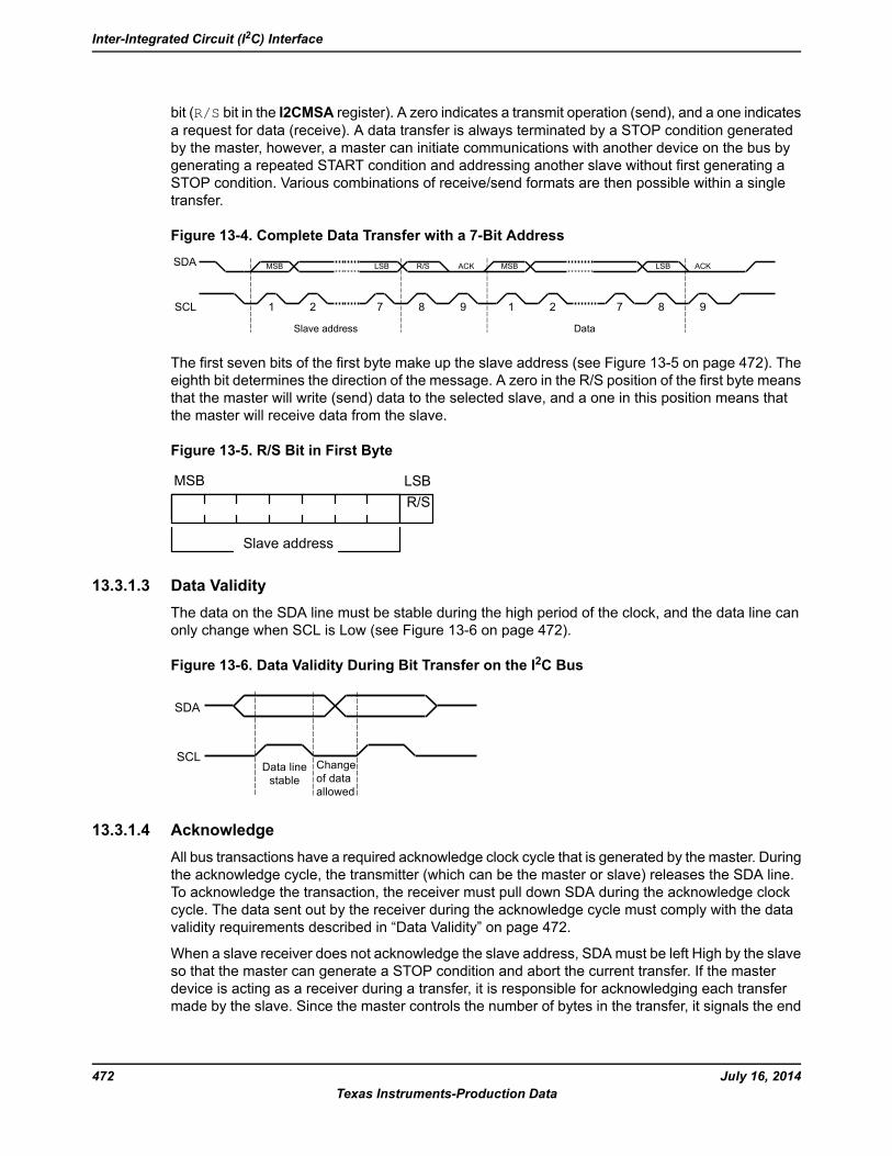
bit (R/S bit in the I2CMSA register). A zero indicates a transmit operation (send), and a one indicatesa request for data (receive). A data transfer is always terminated by a STOP condition generatedby the master, however, a master can initiate communications with another device on the bus bygenerating a repeated START condition and addressing another slave without first generating aSTOP condition. Various combinations of receive/send formats are then possible within a singletransfer.
Figure 13-4. Complete Data Transfer with a 7-Bit Address
DataSlave address
ACKLSBMSBACKR/SLSBMSBSDA
SCL 1 2 7 8 9 1 2 7 8 9
The first seven bits of the first byte make up the slave address (see Figure 13-5 on page 472). Theeighth bit determines the direction of the message. A zero in the R/S position of the first byte meansthat the master will write (send) data to the selected slave, and a one in this position means thatthe master will receive data from the slave.
Figure 13-5. R/S Bit in First Byte
R/SLSB
Slave address
MSB
13.3.1.3 Data ValidityThe data on the SDA line must be stable during the high period of the clock, and the data line canonly change when SCL is Low (see Figure 13-6 on page 472).
Figure 13-6. Data Validity During Bit Transfer on the I2C Bus
Changeof dataallowed
Data linestable
SDA
SCL
13.3.1.4 AcknowledgeAll bus transactions have a required acknowledge clock cycle that is generated by the master. Duringthe acknowledge cycle, the transmitter (which can be the master or slave) releases the SDA line.To acknowledge the transaction, the receiver must pull down SDA during the acknowledge clockcycle. The data sent out by the receiver during the acknowledge cycle must comply with the datavalidity requirements described in “Data Validity” on page 472.
When a slave receiver does not acknowledge the slave address, SDAmust be left High by the slaveso that the master can generate a STOP condition and abort the current transfer. If the masterdevice is acting as a receiver during a transfer, it is responsible for acknowledging each transfermade by the slave. Since the master controls the number of bytes in the transfer, it signals the end
July 16, 2014472Texas Instruments-Production Data
Inter-Integrated Circuit (I2C) Interface
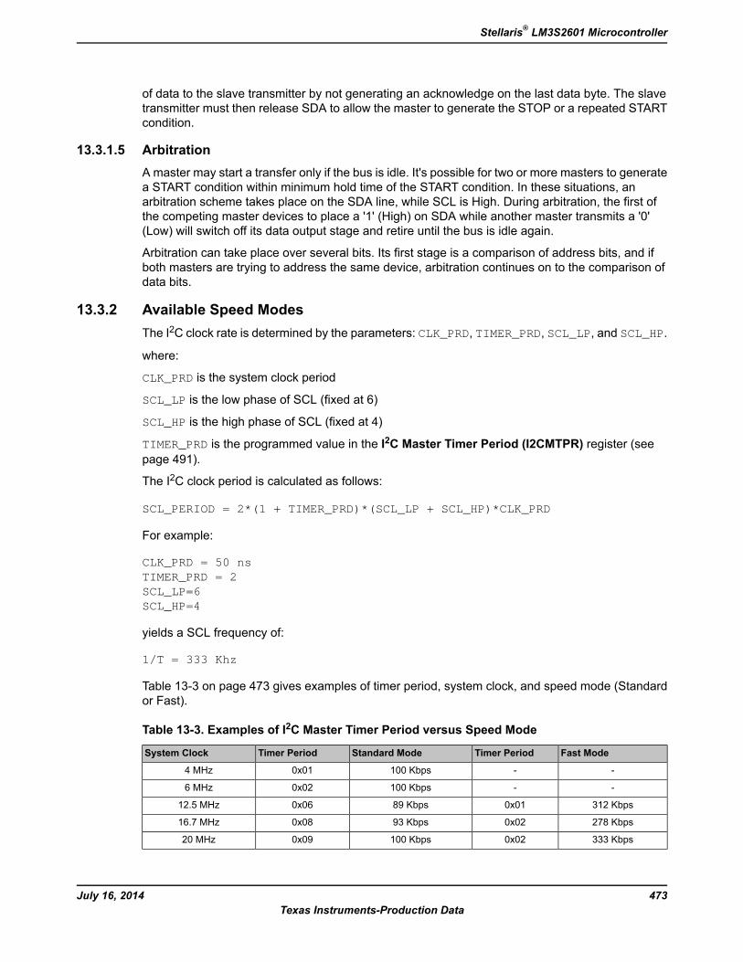
of data to the slave transmitter by not generating an acknowledge on the last data byte. The slavetransmitter must then release SDA to allow the master to generate the STOP or a repeated STARTcondition.
13.3.1.5 ArbitrationA master may start a transfer only if the bus is idle. It's possible for two or more masters to generatea START condition within minimum hold time of the START condition. In these situations, anarbitration scheme takes place on the SDA line, while SCL is High. During arbitration, the first ofthe competing master devices to place a '1' (High) on SDA while another master transmits a '0'(Low) will switch off its data output stage and retire until the bus is idle again.
Arbitration can take place over several bits. Its first stage is a comparison of address bits, and ifboth masters are trying to address the same device, arbitration continues on to the comparison ofdata bits.
13.3.2 Available Speed ModesThe I2C clock rate is determined by the parameters: CLK_PRD, TIMER_PRD, SCL_LP, and SCL_HP.
where:
CLK_PRD is the system clock period
SCL_LP is the low phase of SCL (fixed at 6)
SCL_HP is the high phase of SCL (fixed at 4)
TIMER_PRD is the programmed value in the I2C Master Timer Period (I2CMTPR) register (seepage 491).
The I2C clock period is calculated as follows:
SCL_PERIOD = 2*(1 + TIMER_PRD)*(SCL_LP + SCL_HP)*CLK_PRD
For example:
CLK_PRD = 50 nsTIMER_PRD = 2SCL_LP=6SCL_HP=4
yields a SCL frequency of:
1/T = 333 Khz
Table 13-3 on page 473 gives examples of timer period, system clock, and speed mode (Standardor Fast).
Table 13-3. Examples of I2C Master Timer Period versus Speed Mode
Fast ModeTimer PeriodStandard ModeTimer PeriodSystem Clock
--100 Kbps0x014 MHz
--100 Kbps0x026 MHz
312 Kbps0x0189 Kbps0x0612.5 MHz
278 Kbps0x0293 Kbps0x0816.7 MHz
333 Kbps0x02100 Kbps0x0920 MHz
473July 16, 2014Texas Instruments-Production Data
Stellaris® LM3S2601 Microcontroller
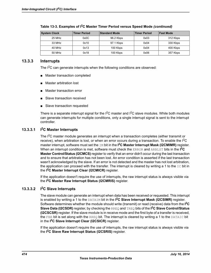
Table 13-3. Examples of I2C Master Timer Period versus Speed Mode (continued)
Fast ModeTimer PeriodStandard ModeTimer PeriodSystem Clock
312 Kbps0x0396.2 Kbps0x0C25 MHz
330 Kbps0x0497.1 Kbps0x1033 MHz
400 Kbps0x04100 Kbps0x1340 MHz
357 Kbps0x06100 Kbps0x1850 MHz
13.3.3 InterruptsThe I2C can generate interrupts when the following conditions are observed:
Master transaction completed
Master arbitration lost
Master transaction error
Slave transaction received
Slave transaction requested
There is a separate interrupt signal for the I2C master and I2C slave modules. While both modulescan generate interrupts for multiple conditions, only a single interrupt signal is sent to the interruptcontroller.
13.3.3.1 I2C Master InterruptsThe I2C master module generates an interrupt when a transaction completes (either transmit orreceive), when arbitration is lost, or when an error occurs during a transaction. To enable the I2Cmaster interrupt, software must set the IM bit in the I2CMaster Interrupt Mask (I2CMIMR) register.When an interrupt condition is met, software must check the ERROR and ARBLST bits in the I2CMaster Control/Status (I2CMCS) register to verify that an error didn't occur during the last transactionand to ensure that arbitration has not been lost. An error condition is asserted if the last transactionwasn't acknowledged by the slave. If an error is not detected and the master has not lost arbitration,the application can proceed with the transfer. The interrupt is cleared by writing a 1 to the IC bit inthe I2C Master Interrupt Clear (I2CMICR) register.
If the application doesn't require the use of interrupts, the raw interrupt status is always visible viathe I2C Master Raw Interrupt Status (I2CMRIS) register.
13.3.3.2 I2C Slave InterruptsThe slave module can generate an interrupt when data has been received or requested. This interruptis enabled by writing a 1 to the DATAIM bit in the I2C Slave Interrupt Mask (I2CSIMR) register.Software determines whether the module should write (transmit) or read (receive) data from the I2CSlave Data (I2CSDR) register, by checking the RREQ and TREQ bits of the I2C Slave Control/Status(I2CSCSR) register. If the slave module is in receive mode and the first byte of a transfer is received,the FBR bit is set along with the RREQ bit. The interrupt is cleared by writing a 1 to the DATAIC bitin the I2C Slave Interrupt Clear (I2CSICR) register.
If the application doesn't require the use of interrupts, the raw interrupt status is always visible viathe I2C Slave Raw Interrupt Status (I2CSRIS) register.
July 16, 2014474Texas Instruments-Production Data
Inter-Integrated Circuit (I2C) Interface
13.3.4 Loopback OperationThe I2C modules can be placed into an internal loopback mode for diagnostic or debug work. Thisis accomplished by setting the LPBK bit in the I2C Master Configuration (I2CMCR) register. Inloopback mode, the SDA and SCL signals from the master and slave modules are tied together.
13.3.5 Command Sequence Flow ChartsThis section details the steps required to perform the various I2C transfer types in both master andslave mode.
13.3.5.1 I2C Master Command SequencesThe figures that follow show the command sequences available for the I2C master.
475July 16, 2014Texas Instruments-Production Data
Stellaris® LM3S2601 Microcontroller
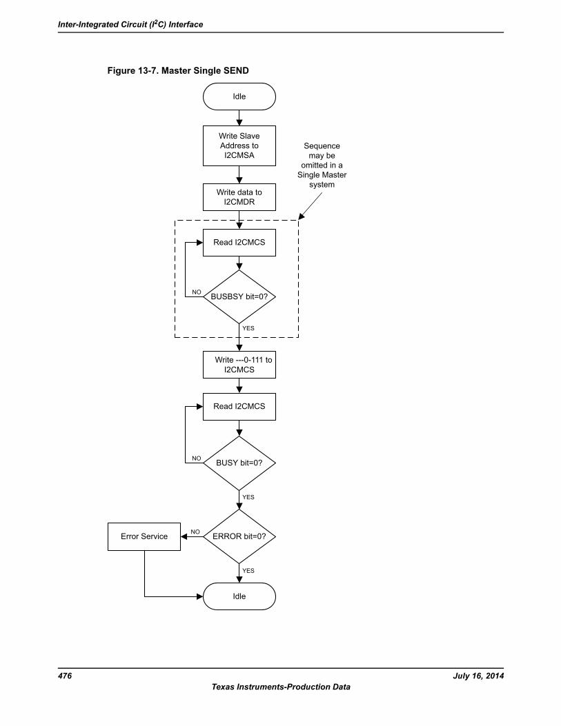
Figure 13-7. Master Single SEND
Idle
Write SlaveAddress toI2CMSA
Write data toI2CMDR
Read I2CMCS
Sequencemay be
omitted in aSingle Master
system
BUSBSY bit=0?NO
Write ---0-111 toI2CMCS
YES
Read I2CMCS
BUSY bit=0?
ERROR bit=0?
YES
Error Service
Idle
YES
NO
NO
July 16, 2014476Texas Instruments-Production Data
Inter-Integrated Circuit (I2C) Interface
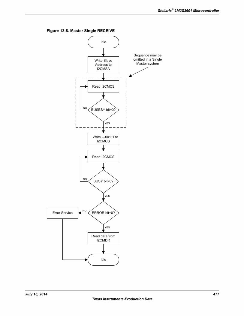
Figure 13-8. Master Single RECEIVE
Idle
Write SlaveAddress toI2CMSA
Read I2CMCS
Sequence may beomitted in a SingleMaster system
BUSBSY bit=0?NO
Write ---00111 toI2CMCS
YES
Read I2CMCS
BUSY bit=0?
ERROR bit=0?
YES
Error Service
Idle
NO
NO
Read data fromI2CMDR
YES
477July 16, 2014Texas Instruments-Production Data
Stellaris® LM3S2601 Microcontroller
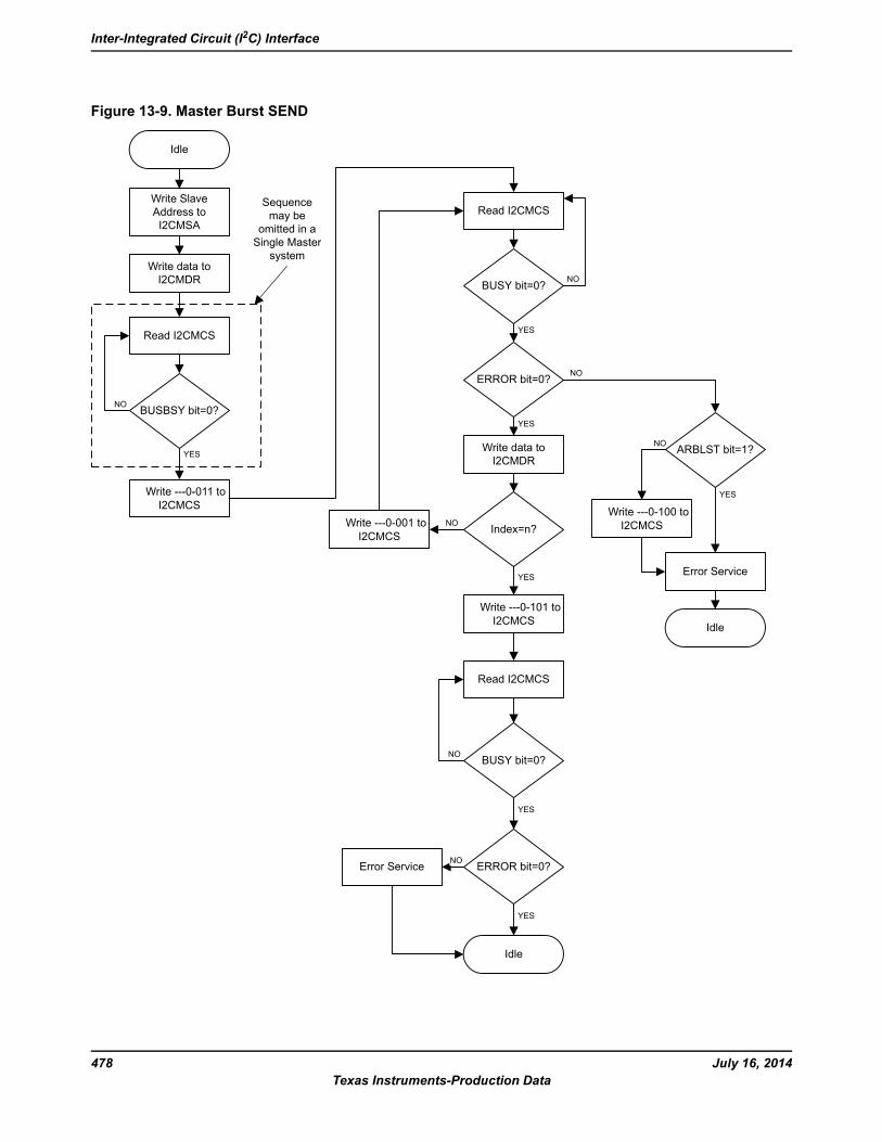
Figure 13-9. Master Burst SEND
Idle
Write SlaveAddress toI2CMSA
Write data toI2CMDR
Read I2CMCS
BUSBSY bit=0?
YES
Write ---0-011 toI2CMCS
NO
Read I2CMCS
BUSY bit=0?
YES
ERROR bit=0?
YES
ARBLST bit=1?Write data toI2CMDR
Write ---0-100 toI2CMCSIndex=n?
NO
Error Service
Idle
YES
Write ---0-001 toI2CMCS
Write ---0-101 toI2CMCS
YES
Read I2CMCS
BUSY bit=0?
ERROR bit=0?
YES
NO
Idle
YES
Error Service NO
NO
NO
NO
Sequencemay be
omitted in aSingle Master
system
July 16, 2014478Texas Instruments-Production Data
Inter-Integrated Circuit (I2C) Interface
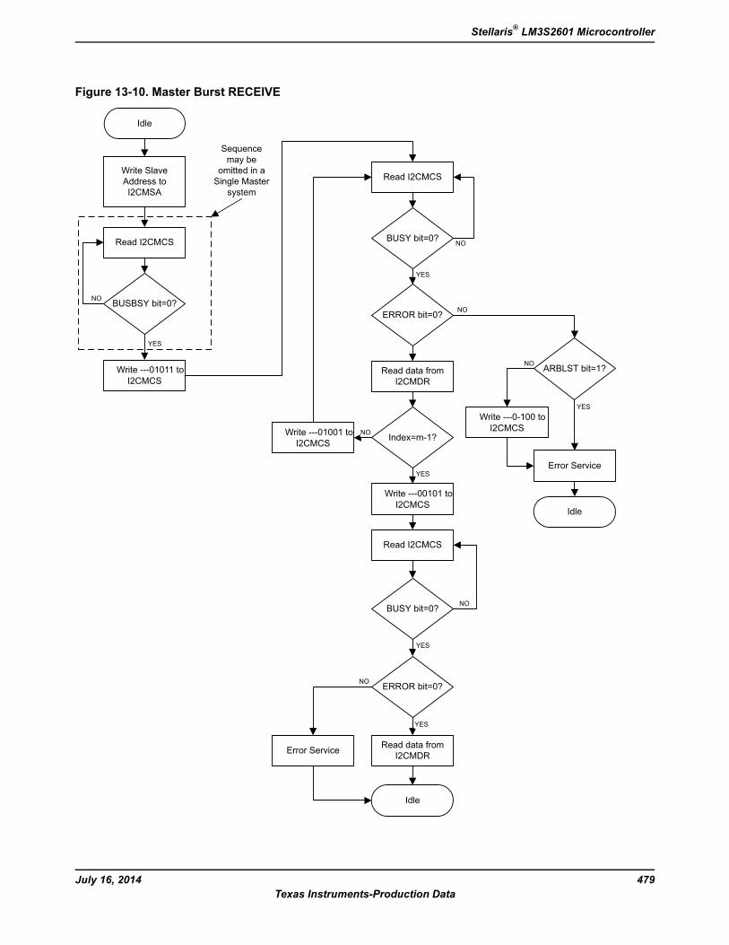
Figure 13-10. Master Burst RECEIVE
Idle
Write SlaveAddress toI2CMSA
Read I2CMCS
BUSBSY bit=0?NO
Write ---01011 toI2CMCS
YES
Read I2CMCS
BUSY bit=0? NO
ERROR bit=0?
YES
ARBLST bit=1?
Write ---0-100 toI2CMCS
NO
Error Service
YES
Idle
Read data fromI2CMDR
Index=m-1?
Write ---00101 toI2CMCS
YES
Idle
Read data fromI2CMDRError Service
ERROR bit=0?
YES
Write ---01001 toI2CMCS
Read I2CMCS
BUSY bit=0? NO
YES
Sequencemay be
omitted in aSingle Master
system
NO
NO
NO
479July 16, 2014Texas Instruments-Production Data
Stellaris® LM3S2601 Microcontroller
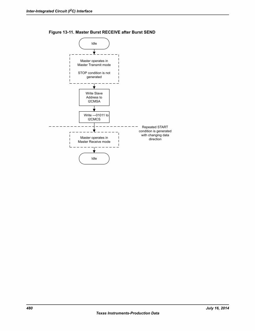
Figure 13-11. Master Burst RECEIVE after Burst SEND
Idle
Master operates inMaster Transmit mode
STOP condition is notgenerated
Write SlaveAddress toI2CMSA
Write ---01011 toI2CMCS
Master operates inMaster Receive mode
Idle
Repeated STARTcondition is generatedwith changing data
direction
July 16, 2014480Texas Instruments-Production Data
Inter-Integrated Circuit (I2C) Interface
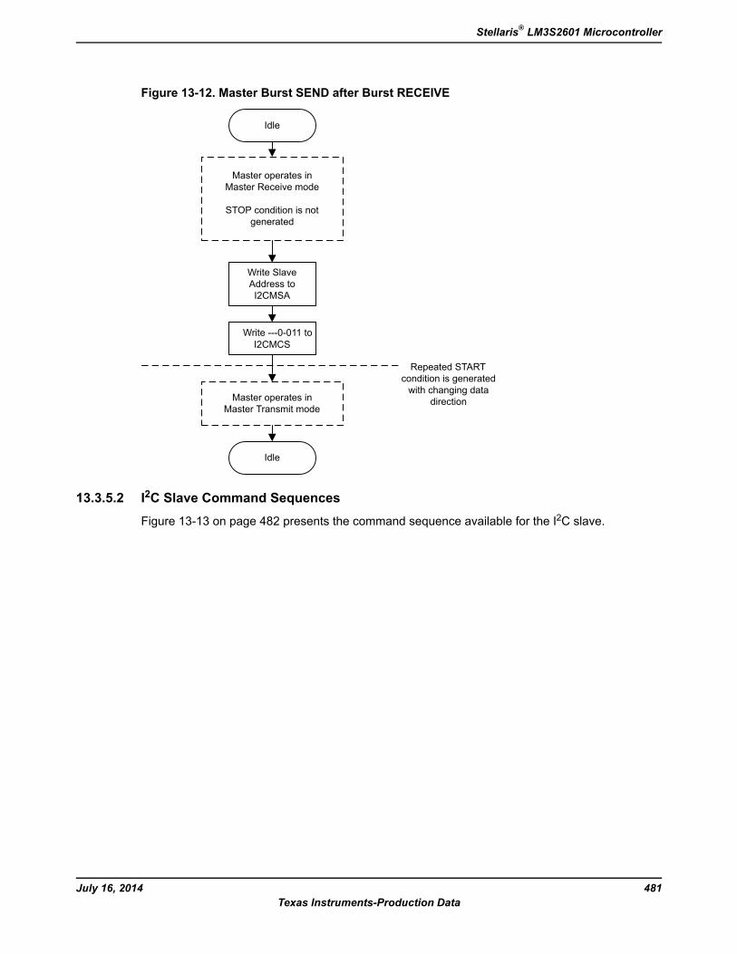
Figure 13-12. Master Burst SEND after Burst RECEIVE
Idle
Master operates inMaster Receive mode
STOP condition is notgenerated
Write SlaveAddress toI2CMSA
Write ---0-011 toI2CMCS
Master operates inMaster Transmit mode
Idle
Repeated STARTcondition is generatedwith changing data
direction
13.3.5.2 I2C Slave Command SequencesFigure 13-13 on page 482 presents the command sequence available for the I2C slave.
481July 16, 2014Texas Instruments-Production Data
Stellaris® LM3S2601 Microcontroller
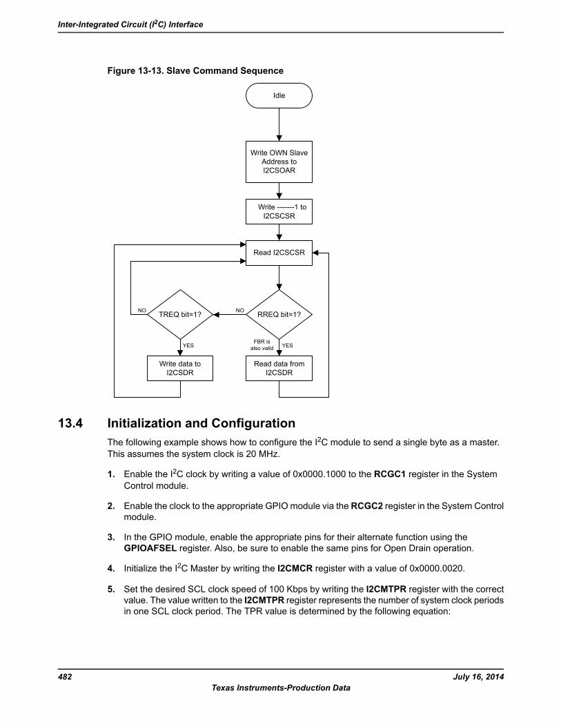
Figure 13-13. Slave Command Sequence
Idle
Write OWN SlaveAddress toI2CSOAR
Write -------1 toI2CSCSR
Read I2CSCSR
RREQ bit=1?
Read data fromI2CSDR
YES
TREQ bit=1? NO
Write data toI2CSDR
YES
NO
FBR isalso valid
13.4 Initialization and ConfigurationThe following example shows how to configure the I2C module to send a single byte as a master.This assumes the system clock is 20 MHz.
1. Enable the I2C clock by writing a value of 0x0000.1000 to the RCGC1 register in the SystemControl module.
2. Enable the clock to the appropriate GPIO module via the RCGC2 register in the System Controlmodule.
3. In the GPIO module, enable the appropriate pins for their alternate function using theGPIOAFSEL register. Also, be sure to enable the same pins for Open Drain operation.
4. Initialize the I2C Master by writing the I2CMCR register with a value of 0x0000.0020.
5. Set the desired SCL clock speed of 100 Kbps by writing the I2CMTPR register with the correctvalue. The value written to the I2CMTPR register represents the number of system clock periodsin one SCL clock period. The TPR value is determined by the following equation:
July 16, 2014482Texas Instruments-Production Data
Inter-Integrated Circuit (I2C) Interface
TPR = (System Clock / (2 * (SCL_LP + SCL_HP) * SCL_CLK)) - 1;TPR = (20MHz / (2 * (6 + 4) * 100000)) - 1;TPR = 9
Write the I2CMTPR register with the value of 0x0000.0009.
6. Specify the slave address of the master and that the next operation will be a Send by writingthe I2CMSA register with a value of 0x0000.0076. This sets the slave address to 0x3B.
7. Place data (byte) to be sent in the data register by writing the I2CMDR register with the desireddata.
8. Initiate a single byte send of the data from Master to Slave by writing the I2CMCS register witha value of 0x0000.0007 (STOP, START, RUN).
9. Wait until the transmission completes by polling the I2CMCS register’s BUSBSY bit until it hasbeen cleared.
13.5 Register MapTable 13-4 on page 483 lists the I2C registers. All addresses given are relative to the I2C baseaddresses for the master and slave:
I2C 0: 0x4002.0000 I2C 1: 0x4002.1000
Note that the I2C module clock must be enabled before the registers can be programmed (seepage 212). There must be a delay of 3 system clocks after the I2C module clock is enabled beforeany I2C module registers are accessed.
The hw_i2c.h file in the StellarisWare® Driver Library uses a base address of 0x800 for the I2C slaveregisters. Be aware when using registers with offsets between 0x800 and 0x818 that StellarisWareuses an offset between 0x000 and 0x018 with the slave base address.
Table 13-4. Inter-Integrated Circuit (I2C) Interface Register Map
SeepageDescriptionResetTypeNameOffset
I2C Master
485I2C Master Slave Address0x0000.0000R/WI2CMSA0x000
486I2C Master Control/Status0x0000.0000R/WI2CMCS0x004
490I2C Master Data0x0000.0000R/WI2CMDR0x008
491I2C Master Timer Period0x0000.0001R/WI2CMTPR0x00C
492I2C Master Interrupt Mask0x0000.0000R/WI2CMIMR0x010
493I2C Master Raw Interrupt Status0x0000.0000ROI2CMRIS0x014
494I2C Master Masked Interrupt Status0x0000.0000ROI2CMMIS0x018
495I2C Master Interrupt Clear0x0000.0000WOI2CMICR0x01C
496I2C Master Configuration0x0000.0000R/WI2CMCR0x020
483July 16, 2014Texas Instruments-Production Data
Stellaris® LM3S2601 Microcontroller
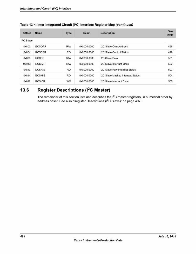
Table 13-4. Inter-Integrated Circuit (I2C) Interface Register Map (continued)
SeepageDescriptionResetTypeNameOffset
I2C Slave
498I2C Slave Own Address0x0000.0000R/WI2CSOAR0x800
499I2C Slave Control/Status0x0000.0000ROI2CSCSR0x804
501I2C Slave Data0x0000.0000R/WI2CSDR0x808
502I2C Slave Interrupt Mask0x0000.0000R/WI2CSIMR0x80C
503I2C Slave Raw Interrupt Status0x0000.0000ROI2CSRIS0x810
504I2C Slave Masked Interrupt Status0x0000.0000ROI2CSMIS0x814
505I2C Slave Interrupt Clear0x0000.0000WOI2CSICR0x818
13.6 Register Descriptions (I2C Master)The remainder of this section lists and describes the I2C master registers, in numerical order byaddress offset. See also “Register Descriptions (I2C Slave)” on page 497.
July 16, 2014484Texas Instruments-Production Data
Inter-Integrated Circuit (I2C) Interface
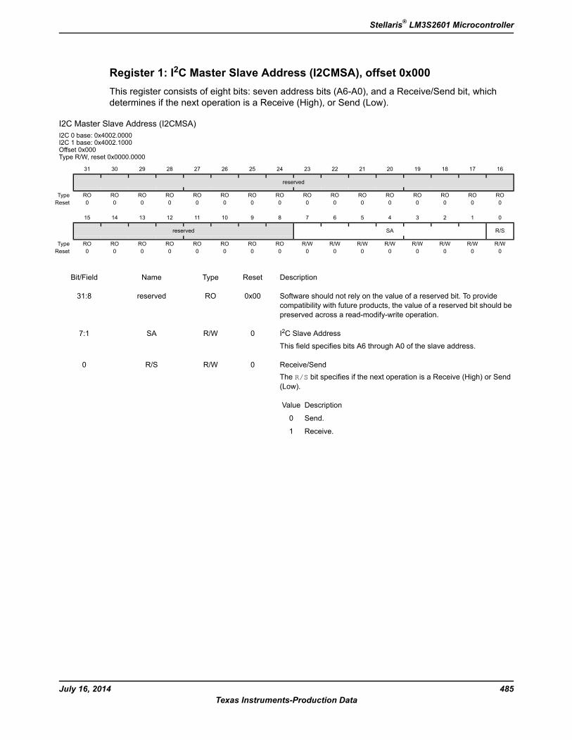
Register 1: I2C Master Slave Address (I2CMSA), offset 0x000This register consists of eight bits: seven address bits (A6-A0), and a Receive/Send bit, whichdetermines if the next operation is a Receive (High), or Send (Low).
I2C Master Slave Address (I2CMSA)I2C 0 base: 0x4002.0000I2C 1 base: 0x4002.1000Offset 0x000Type R/W, reset 0x0000.0000
16171819202122232425262728293031
reserved
ROROROROROROROROROROROROROROROROType0000000000000000Reset
0123456789101112131415
R/SSAreserved
R/WR/WR/WR/WR/WR/WR/WR/WROROROROROROROROType0000000000000000Reset
DescriptionResetTypeNameBit/Field
Software should not rely on the value of a reserved bit. To providecompatibility with future products, the value of a reserved bit should bepreserved across a read-modify-write operation.
0x00ROreserved31:8
I2C Slave Address
This field specifies bits A6 through A0 of the slave address.
0R/WSA7:1
Receive/SendThe R/S bit specifies if the next operation is a Receive (High) or Send(Low).
DescriptionValue
Send.0
Receive.1
0R/WR/S0
485July 16, 2014Texas Instruments-Production Data
Stellaris® LM3S2601 Microcontroller
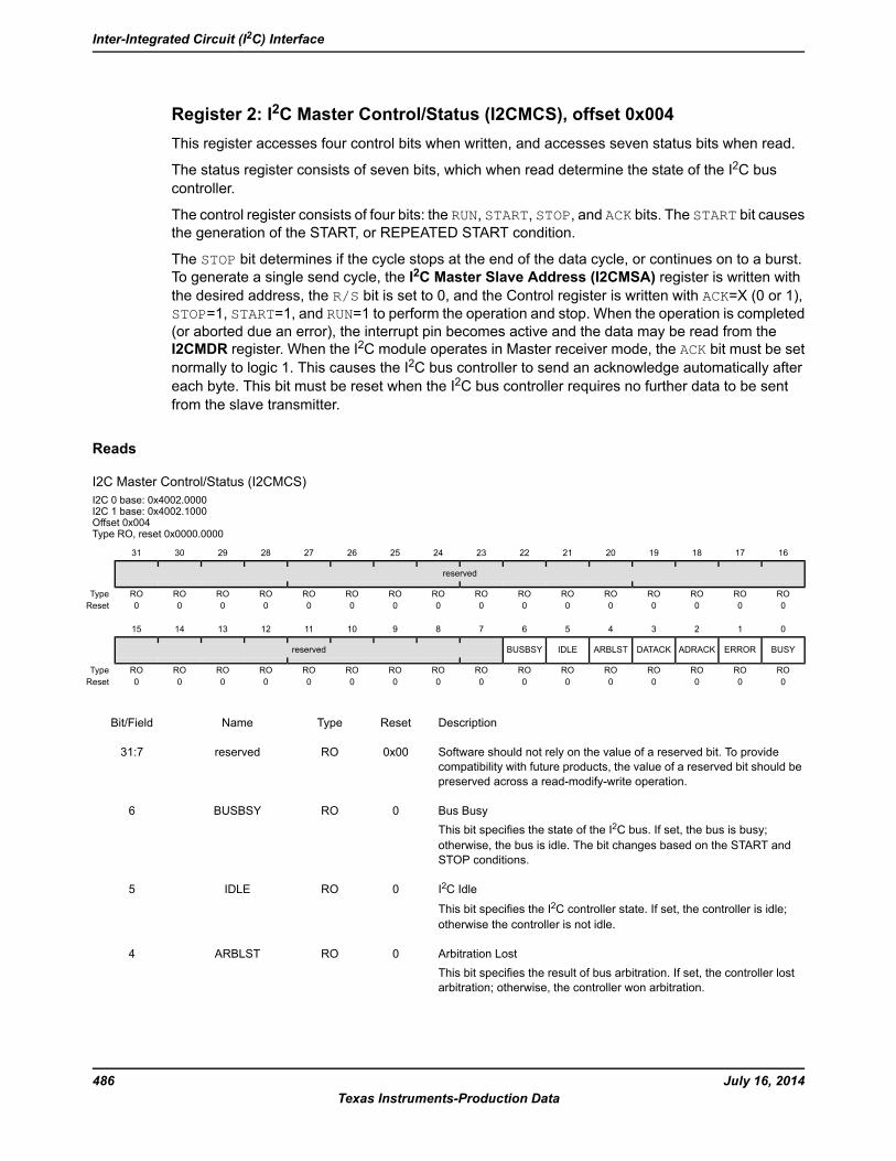
Register 2: I2C Master Control/Status (I2CMCS), offset 0x004This register accesses four control bits when written, and accesses seven status bits when read.
The status register consists of seven bits, which when read determine the state of the I2C buscontroller.
The control register consists of four bits: the RUN, START, STOP, and ACK bits. The START bit causesthe generation of the START, or REPEATED START condition.
The STOP bit determines if the cycle stops at the end of the data cycle, or continues on to a burst.To generate a single send cycle, the I2C Master Slave Address (I2CMSA) register is written withthe desired address, the R/S bit is set to 0, and the Control register is written with ACK=X (0 or 1),STOP=1, START=1, and RUN=1 to perform the operation and stop. When the operation is completed(or aborted due an error), the interrupt pin becomes active and the data may be read from theI2CMDR register. When the I2C module operates in Master receiver mode, the ACK bit must be setnormally to logic 1. This causes the I2C bus controller to send an acknowledge automatically aftereach byte. This bit must be reset when the I2C bus controller requires no further data to be sentfrom the slave transmitter.
Reads
I2C Master Control/Status (I2CMCS)I2C 0 base: 0x4002.0000I2C 1 base: 0x4002.1000Offset 0x004Type RO, reset 0x0000.0000
16171819202122232425262728293031
reserved
ROROROROROROROROROROROROROROROROType0000000000000000Reset
0123456789101112131415
BUSYERRORADRACKDATACKARBLSTIDLEBUSBSYreserved
ROROROROROROROROROROROROROROROROType0000000000000000Reset
DescriptionResetTypeNameBit/Field
Software should not rely on the value of a reserved bit. To providecompatibility with future products, the value of a reserved bit should bepreserved across a read-modify-write operation.
0x00ROreserved31:7
Bus BusyThis bit specifies the state of the I2C bus. If set, the bus is busy;otherwise, the bus is idle. The bit changes based on the START andSTOP conditions.
0ROBUSBSY6
I2C Idle
This bit specifies the I2C controller state. If set, the controller is idle;otherwise the controller is not idle.
0ROIDLE5
Arbitration LostThis bit specifies the result of bus arbitration. If set, the controller lostarbitration; otherwise, the controller won arbitration.
0ROARBLST4
July 16, 2014486Texas Instruments-Production Data
Inter-Integrated Circuit (I2C) Interface
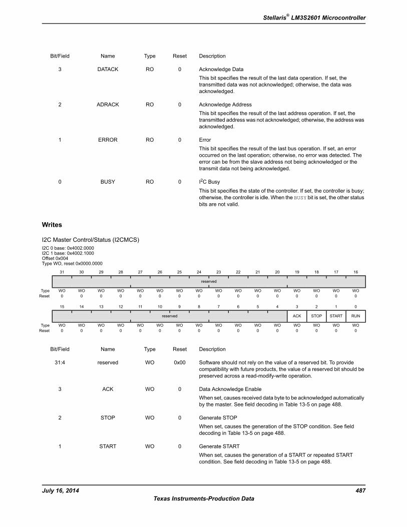
DescriptionResetTypeNameBit/Field
Acknowledge DataThis bit specifies the result of the last data operation. If set, thetransmitted data was not acknowledged; otherwise, the data wasacknowledged.
0RODATACK3
Acknowledge AddressThis bit specifies the result of the last address operation. If set, thetransmitted address was not acknowledged; otherwise, the address wasacknowledged.
0ROADRACK2
ErrorThis bit specifies the result of the last bus operation. If set, an erroroccurred on the last operation; otherwise, no error was detected. Theerror can be from the slave address not being acknowledged or thetransmit data not being acknowledged.
0ROERROR1
I2C Busy
This bit specifies the state of the controller. If set, the controller is busy;otherwise, the controller is idle. When the BUSY bit is set, the other statusbits are not valid.
0ROBUSY0
Writes
I2C Master Control/Status (I2CMCS)I2C 0 base: 0x4002.0000I2C 1 base: 0x4002.1000Offset 0x004Type WO, reset 0x0000.0000
16171819202122232425262728293031
reserved
WOWOWOWOWOWOWOWOWOWOWOWOWOWOWOWOType0000000000000000Reset
0123456789101112131415
RUNSTARTSTOPACKreserved
WOWOWOWOWOWOWOWOWOWOWOWOWOWOWOWOType0000000000000000Reset
DescriptionResetTypeNameBit/Field
Software should not rely on the value of a reserved bit. To providecompatibility with future products, the value of a reserved bit should bepreserved across a read-modify-write operation.
0x00WOreserved31:4
Data Acknowledge EnableWhen set, causes received data byte to be acknowledged automaticallyby the master. See field decoding in Table 13-5 on page 488.
0WOACK3
Generate STOPWhen set, causes the generation of the STOP condition. See fielddecoding in Table 13-5 on page 488.
0WOSTOP2
Generate STARTWhen set, causes the generation of a START or repeated STARTcondition. See field decoding in Table 13-5 on page 488.
0WOSTART1
487July 16, 2014Texas Instruments-Production Data
Stellaris® LM3S2601 Microcontroller
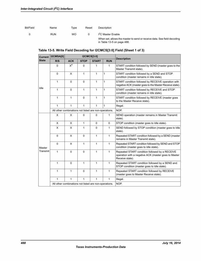
DescriptionResetTypeNameBit/Field
I2C Master Enable
When set, allows the master to send or receive data. See field decodingin Table 13-5 on page 488.
0WORUN0
Table 13-5. Write Field Decoding for I2CMCS[3:0] Field (Sheet 1 of 3)
DescriptionI2CMCS[3:0]I2CMSA[0]Current
State RUNSTARTSTOPACKR/S
START condition followed by SEND (master goes to theMaster Transmit state).
110Xa0
Idle
START condition followed by a SEND and STOPcondition (master remains in Idle state).
111X0
START condition followed by RECEIVE operation withnegative ACK (master goes to theMaster Receive state).
11001
START condition followed by RECEIVE and STOPcondition (master remains in Idle state).
11101
START condition followed by RECEIVE (master goesto the Master Receive state).
11011
Illegal.11111
NOP.All other combinations not listed are non-operations.
SEND operation (master remains in Master Transmitstate).
100XX
MasterTransmit
STOP condition (master goes to Idle state).001XX
SEND followed by STOP condition (master goes to Idlestate).
101XX
Repeated START condition followed by a SEND (masterremains in Master Transmit state).
110X0
Repeated START condition followed by SENDand STOPcondition (master goes to Idle state).
111X0
Repeated START condition followed by a RECEIVEoperation with a negative ACK (master goes to MasterReceive state).
11001
Repeated START condition followed by a SEND andSTOP condition (master goes to Idle state).
11101
Repeated START condition followed by RECEIVE(master goes to Master Receive state).
11011
Illegal.11111
NOP.All other combinations not listed are non-operations.
July 16, 2014488Texas Instruments-Production Data
Inter-Integrated Circuit (I2C) Interface
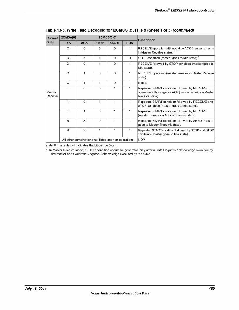
Table 13-5. Write Field Decoding for I2CMCS[3:0] Field (Sheet 1 of 3) (continued)
DescriptionI2CMCS[3:0]I2CMSA[0]Current
State RUNSTARTSTOPACKR/S
RECEIVE operation with negative ACK (master remainsin Master Receive state).
1000X
MasterReceive
STOP condition (master goes to Idle state).b001XX
RECEIVE followed by STOP condition (master goes toIdle state).
1010X
RECEIVE operation (master remains in Master Receivestate).
1001X
Illegal.1011X
Repeated START condition followed by RECEIVEoperation with a negative ACK (master remains in MasterReceive state).
11001
Repeated START condition followed by RECEIVE andSTOP condition (master goes to Idle state).
11101
Repeated START condition followed by RECEIVE(master remains in Master Receive state).
11011
Repeated START condition followed by SEND (mastergoes to Master Transmit state).
110X0
Repeated START condition followed by SENDand STOPcondition (master goes to Idle state).
111X0
NOP.All other combinations not listed are non-operations.
a. An X in a table cell indicates the bit can be 0 or 1.b. In Master Receive mode, a STOP condition should be generated only after a Data Negative Acknowledge executed by
the master or an Address Negative Acknowledge executed by the slave.
489July 16, 2014Texas Instruments-Production Data
Stellaris® LM3S2601 Microcontroller
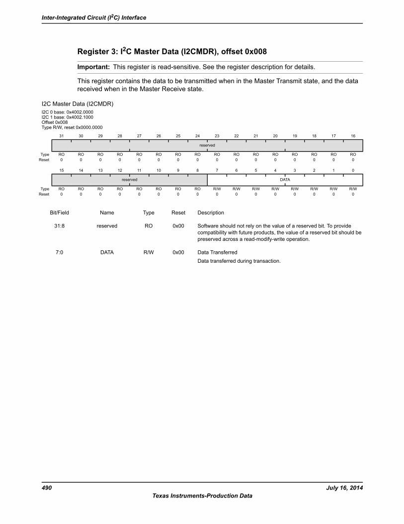
Register 3: I2C Master Data (I2CMDR), offset 0x008
Important: This register is read-sensitive. See the register description for details.
This register contains the data to be transmitted when in the Master Transmit state, and the datareceived when in the Master Receive state.
I2C Master Data (I2CMDR)I2C 0 base: 0x4002.0000I2C 1 base: 0x4002.1000Offset 0x008Type R/W, reset 0x0000.0000
16171819202122232425262728293031
reserved
ROROROROROROROROROROROROROROROROType0000000000000000Reset
0123456789101112131415
DATAreserved
R/WR/WR/WR/WR/WR/WR/WR/WROROROROROROROROType0000000000000000Reset
DescriptionResetTypeNameBit/Field
Software should not rely on the value of a reserved bit. To providecompatibility with future products, the value of a reserved bit should bepreserved across a read-modify-write operation.
0x00ROreserved31:8
Data TransferredData transferred during transaction.
0x00R/WDATA7:0
July 16, 2014490Texas Instruments-Production Data
Inter-Integrated Circuit (I2C) Interface
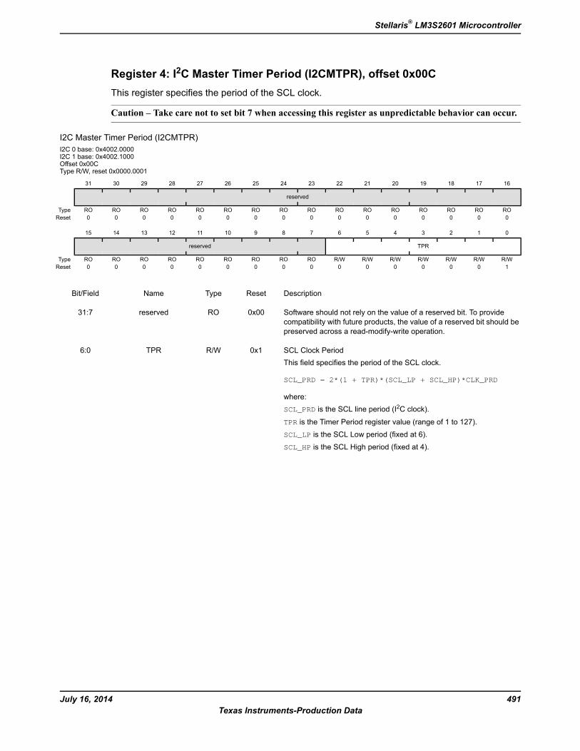
Register 4: I2C Master Timer Period (I2CMTPR), offset 0x00CThis register specifies the period of the SCL clock.
Caution – Take care not to set bit 7 when accessing this register as unpredictable behavior can occur.
I2C Master Timer Period (I2CMTPR)I2C 0 base: 0x4002.0000I2C 1 base: 0x4002.1000Offset 0x00CType R/W, reset 0x0000.0001
16171819202122232425262728293031
reserved
ROROROROROROROROROROROROROROROROType0000000000000000Reset
0123456789101112131415
TPRreserved
R/WR/WR/WR/WR/WR/WR/WROROROROROROROROROType1000000000000000Reset
DescriptionResetTypeNameBit/Field
Software should not rely on the value of a reserved bit. To providecompatibility with future products, the value of a reserved bit should bepreserved across a read-modify-write operation.
0x00ROreserved31:7
SCL Clock PeriodThis field specifies the period of the SCL clock.
SCL_PRD = 2*(1 + TPR)*(SCL_LP + SCL_HP)*CLK_PRD
where:SCL_PRD is the SCL line period (I2C clock).
TPR is the Timer Period register value (range of 1 to 127).SCL_LP is the SCL Low period (fixed at 6).SCL_HP is the SCL High period (fixed at 4).
0x1R/WTPR6:0
491July 16, 2014Texas Instruments-Production Data
Stellaris® LM3S2601 Microcontroller
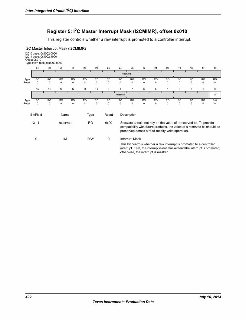
Register 5: I2C Master Interrupt Mask (I2CMIMR), offset 0x010This register controls whether a raw interrupt is promoted to a controller interrupt.
I2C Master Interrupt Mask (I2CMIMR)I2C 0 base: 0x4002.0000I2C 1 base: 0x4002.1000Offset 0x010Type R/W, reset 0x0000.0000
16171819202122232425262728293031
reserved
ROROROROROROROROROROROROROROROROType0000000000000000Reset
0123456789101112131415
IMreserved
R/WROROROROROROROROROROROROROROROType0000000000000000Reset
DescriptionResetTypeNameBit/Field
Software should not rely on the value of a reserved bit. To providecompatibility with future products, the value of a reserved bit should bepreserved across a read-modify-write operation.
0x00ROreserved31:1
Interrupt MaskThis bit controls whether a raw interrupt is promoted to a controllerinterrupt. If set, the interrupt is not masked and the interrupt is promoted;otherwise, the interrupt is masked.
0R/WIM0
July 16, 2014492Texas Instruments-Production Data
Inter-Integrated Circuit (I2C) Interface
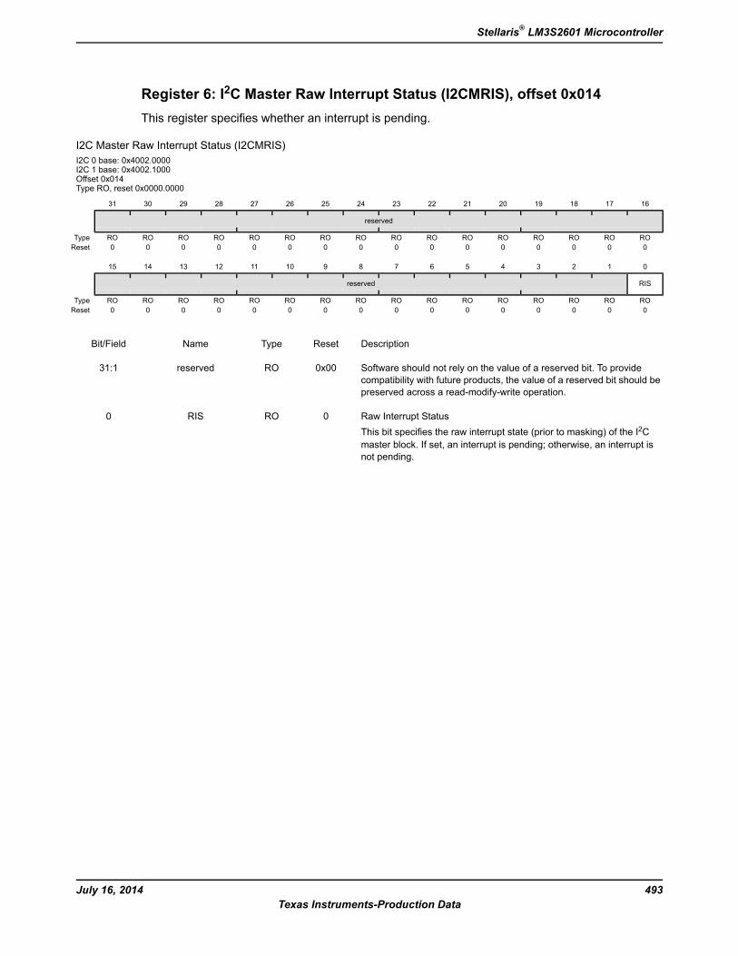
Register 6: I2C Master Raw Interrupt Status (I2CMRIS), offset 0x014This register specifies whether an interrupt is pending.
I2C Master Raw Interrupt Status (I2CMRIS)I2C 0 base: 0x4002.0000I2C 1 base: 0x4002.1000Offset 0x014Type RO, reset 0x0000.0000
16171819202122232425262728293031
reserved
ROROROROROROROROROROROROROROROROType0000000000000000Reset
0123456789101112131415
RISreserved
ROROROROROROROROROROROROROROROROType0000000000000000Reset
DescriptionResetTypeNameBit/Field
Software should not rely on the value of a reserved bit. To providecompatibility with future products, the value of a reserved bit should bepreserved across a read-modify-write operation.
0x00ROreserved31:1
Raw Interrupt StatusThis bit specifies the raw interrupt state (prior to masking) of the I2Cmaster block. If set, an interrupt is pending; otherwise, an interrupt isnot pending.
0RORIS0
493July 16, 2014Texas Instruments-Production Data
Stellaris® LM3S2601 Microcontroller
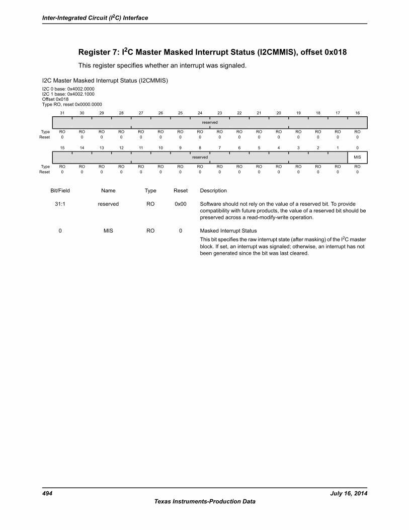
Register 7: I2C Master Masked Interrupt Status (I2CMMIS), offset 0x018This register specifies whether an interrupt was signaled.
I2C Master Masked Interrupt Status (I2CMMIS)I2C 0 base: 0x4002.0000I2C 1 base: 0x4002.1000Offset 0x018Type RO, reset 0x0000.0000
16171819202122232425262728293031
reserved
ROROROROROROROROROROROROROROROROType0000000000000000Reset
0123456789101112131415
MISreserved
ROROROROROROROROROROROROROROROROType0000000000000000Reset
DescriptionResetTypeNameBit/Field
Software should not rely on the value of a reserved bit. To providecompatibility with future products, the value of a reserved bit should bepreserved across a read-modify-write operation.
0x00ROreserved31:1
Masked Interrupt StatusThis bit specifies the raw interrupt state (after masking) of the I2Cmasterblock. If set, an interrupt was signaled; otherwise, an interrupt has notbeen generated since the bit was last cleared.
0ROMIS0
July 16, 2014494Texas Instruments-Production Data
Inter-Integrated Circuit (I2C) Interface
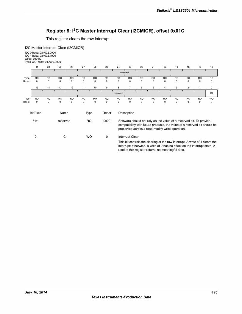
Register 8: I2C Master Interrupt Clear (I2CMICR), offset 0x01CThis register clears the raw interrupt.
I2C Master Interrupt Clear (I2CMICR)I2C 0 base: 0x4002.0000I2C 1 base: 0x4002.1000Offset 0x01CType WO, reset 0x0000.0000
16171819202122232425262728293031
reserved
ROROROROROROROROROROROROROROROROType0000000000000000Reset
0123456789101112131415
ICreserved
WOROROROROROROROROROROROROROROROType0000000000000000Reset
DescriptionResetTypeNameBit/Field
Software should not rely on the value of a reserved bit. To providecompatibility with future products, the value of a reserved bit should bepreserved across a read-modify-write operation.
0x00ROreserved31:1
Interrupt ClearThis bit controls the clearing of the raw interrupt. A write of 1 clears theinterrupt; otherwise, a write of 0 has no affect on the interrupt state. Aread of this register returns no meaningful data.
0WOIC0
495July 16, 2014Texas Instruments-Production Data
Stellaris® LM3S2601 Microcontroller
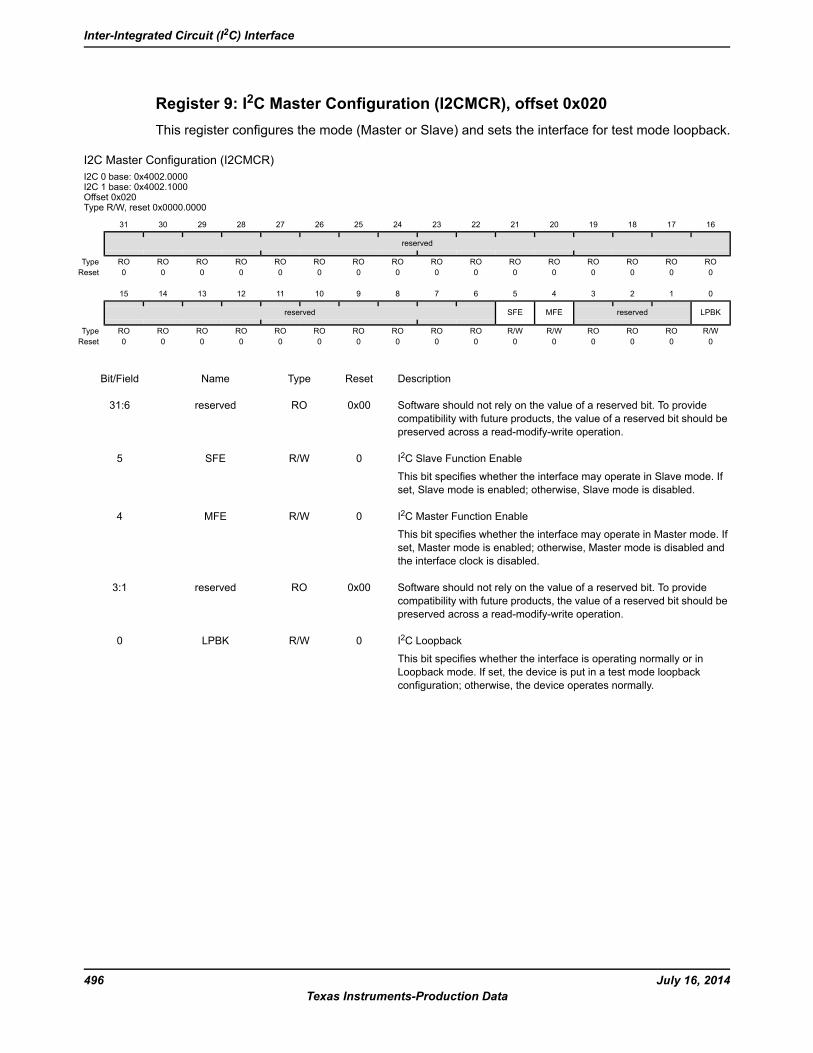
Register 9: I2C Master Configuration (I2CMCR), offset 0x020This register configures the mode (Master or Slave) and sets the interface for test mode loopback.
I2C Master Configuration (I2CMCR)I2C 0 base: 0x4002.0000I2C 1 base: 0x4002.1000Offset 0x020Type R/W, reset 0x0000.0000
16171819202122232425262728293031
reserved
ROROROROROROROROROROROROROROROROType0000000000000000Reset
0123456789101112131415
LPBKreservedMFESFEreserved
R/WROROROR/WR/WROROROROROROROROROROType0000000000000000Reset
DescriptionResetTypeNameBit/Field
Software should not rely on the value of a reserved bit. To providecompatibility with future products, the value of a reserved bit should bepreserved across a read-modify-write operation.
0x00ROreserved31:6
I2C Slave Function Enable
This bit specifies whether the interface may operate in Slave mode. Ifset, Slave mode is enabled; otherwise, Slave mode is disabled.
0R/WSFE5
I2C Master Function Enable
This bit specifies whether the interface may operate in Master mode. Ifset, Master mode is enabled; otherwise, Master mode is disabled andthe interface clock is disabled.
0R/WMFE4
Software should not rely on the value of a reserved bit. To providecompatibility with future products, the value of a reserved bit should bepreserved across a read-modify-write operation.
0x00ROreserved3:1
I2C Loopback
This bit specifies whether the interface is operating normally or inLoopback mode. If set, the device is put in a test mode loopbackconfiguration; otherwise, the device operates normally.
0R/WLPBK0
July 16, 2014496Texas Instruments-Production Data
Inter-Integrated Circuit (I2C) Interface
13.7 Register Descriptions (I2C Slave)The remainder of this section lists and describes the I2C slave registers, in numerical order byaddress offset. See also “Register Descriptions (I2C Master)” on page 484.
497July 16, 2014Texas Instruments-Production Data
Stellaris® LM3S2601 Microcontroller
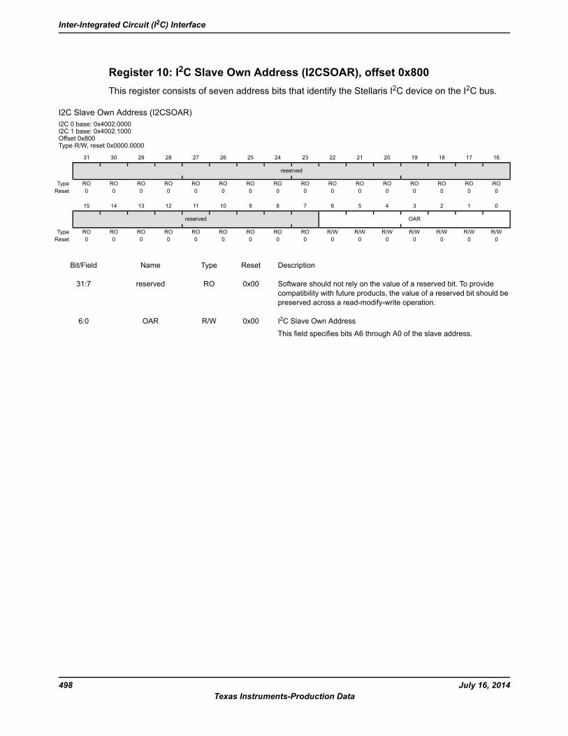
Register 10: I2C Slave Own Address (I2CSOAR), offset 0x800This register consists of seven address bits that identify the Stellaris I2C device on the I2C bus.
I2C Slave Own Address (I2CSOAR)I2C 0 base: 0x4002.0000I2C 1 base: 0x4002.1000Offset 0x800Type R/W, reset 0x0000.0000
16171819202122232425262728293031
reserved
ROROROROROROROROROROROROROROROROType0000000000000000Reset
0123456789101112131415
OARreserved
R/WR/WR/WR/WR/WR/WR/WROROROROROROROROROType0000000000000000Reset
DescriptionResetTypeNameBit/Field
Software should not rely on the value of a reserved bit. To providecompatibility with future products, the value of a reserved bit should bepreserved across a read-modify-write operation.
0x00ROreserved31:7
I2C Slave Own Address
This field specifies bits A6 through A0 of the slave address.
0x00R/WOAR6:0
July 16, 2014498Texas Instruments-Production Data
Inter-Integrated Circuit (I2C) Interface
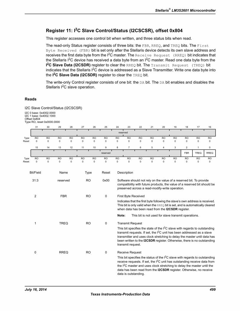
Register 11: I2C Slave Control/Status (I2CSCSR), offset 0x804This register accesses one control bit when written, and three status bits when read.
The read-only Status register consists of three bits: the FBR, RREQ, and TREQ bits. The FirstByte Received (FBR) bit is set only after the Stellaris device detects its own slave address andreceives the first data byte from the I2C master. The Receive Request (RREQ) bit indicates thatthe Stellaris I2C device has received a data byte from an I2C master. Read one data byte from theI2C Slave Data (I2CSDR) register to clear the RREQ bit. The Transmit Request (TREQ) bitindicates that the Stellaris I2C device is addressed as a Slave Transmitter. Write one data byte intothe I2C Slave Data (I2CSDR) register to clear the TREQ bit.
The write-only Control register consists of one bit: the DA bit. The DA bit enables and disables theStellaris I2C slave operation.
Reads
I2C Slave Control/Status (I2CSCSR)I2C 0 base: 0x4002.0000I2C 1 base: 0x4002.1000Offset 0x804Type RO, reset 0x0000.0000
16171819202122232425262728293031
reserved
ROROROROROROROROROROROROROROROROType0000000000000000Reset
0123456789101112131415
RREQTREQFBRreserved
ROROROROROROROROROROROROROROROROType0000000000000000Reset
DescriptionResetTypeNameBit/Field
Software should not rely on the value of a reserved bit. To providecompatibility with future products, the value of a reserved bit should bepreserved across a read-modify-write operation.
0x00ROreserved31:3
First Byte ReceivedIndicates that the first byte following the slave’s own address is received.This bit is only valid when the RREQ bit is set, and is automatically clearedwhen data has been read from the I2CSDR register.
Note: This bit is not used for slave transmit operations.
0ROFBR2
Transmit RequestThis bit specifies the state of the I2C slave with regards to outstandingtransmit requests. If set, the I2C unit has been addressed as a slavetransmitter and uses clock stretching to delay the master until data hasbeen written to the I2CSDR register. Otherwise, there is no outstandingtransmit request.
0ROTREQ1
Receive RequestThis bit specifies the status of the I2C slave with regards to outstandingreceive requests. If set, the I2C unit has outstanding receive data fromthe I2C master and uses clock stretching to delay the master until thedata has been read from the I2CSDR register. Otherwise, no receivedata is outstanding.
0RORREQ0
499July 16, 2014Texas Instruments-Production Data
Stellaris® LM3S2601 Microcontroller
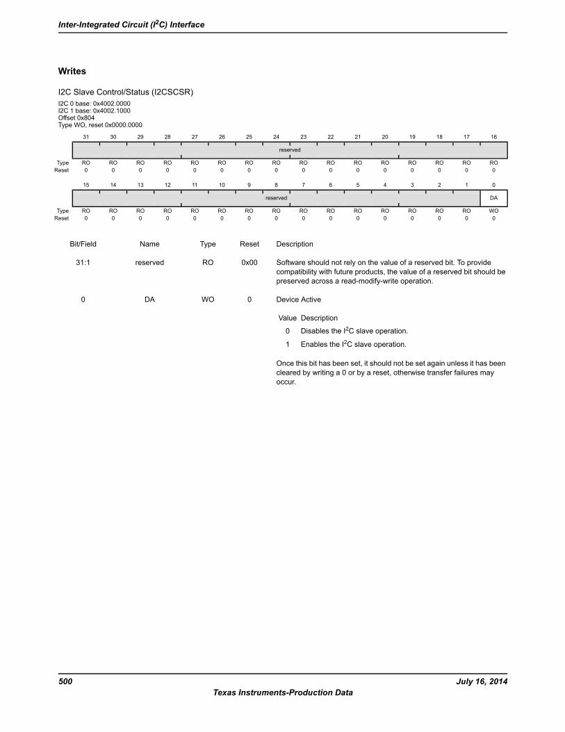
Writes
I2C Slave Control/Status (I2CSCSR)I2C 0 base: 0x4002.0000I2C 1 base: 0x4002.1000Offset 0x804Type WO, reset 0x0000.0000
16171819202122232425262728293031
reserved
ROROROROROROROROROROROROROROROROType0000000000000000Reset
0123456789101112131415
DAreserved
WOROROROROROROROROROROROROROROROType0000000000000000Reset
DescriptionResetTypeNameBit/Field
Software should not rely on the value of a reserved bit. To providecompatibility with future products, the value of a reserved bit should bepreserved across a read-modify-write operation.
0x00ROreserved31:1
Device Active
DescriptionValue
Disables the I2C slave operation.0
Enables the I2C slave operation.1
Once this bit has been set, it should not be set again unless it has beencleared by writing a 0 or by a reset, otherwise transfer failures mayoccur.
0WODA0
July 16, 2014500Texas Instruments-Production Data
Inter-Integrated Circuit (I2C) Interface
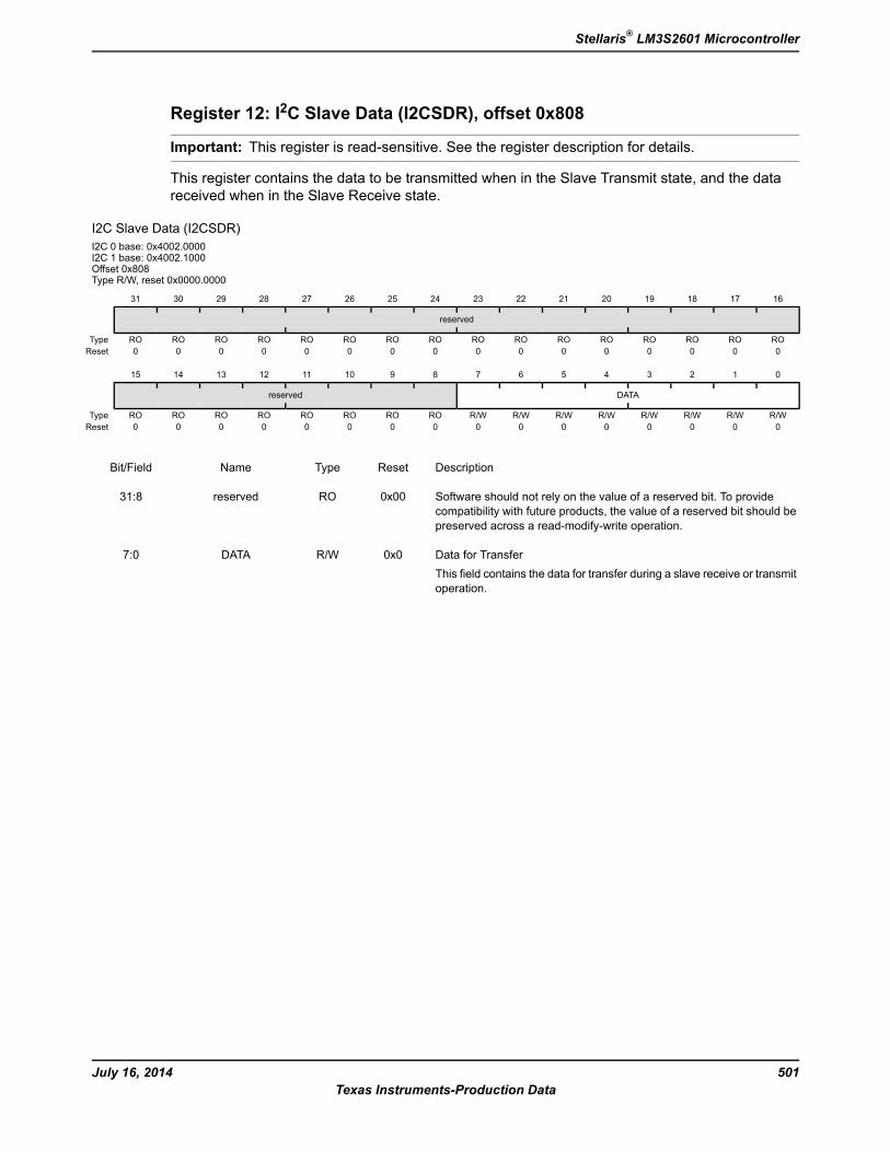
Register 12: I2C Slave Data (I2CSDR), offset 0x808
Important: This register is read-sensitive. See the register description for details.
This register contains the data to be transmitted when in the Slave Transmit state, and the datareceived when in the Slave Receive state.
I2C Slave Data (I2CSDR)I2C 0 base: 0x4002.0000I2C 1 base: 0x4002.1000Offset 0x808Type R/W, reset 0x0000.0000
16171819202122232425262728293031
reserved
ROROROROROROROROROROROROROROROROType0000000000000000Reset
0123456789101112131415
DATAreserved
R/WR/WR/WR/WR/WR/WR/WR/WROROROROROROROROType0000000000000000Reset
DescriptionResetTypeNameBit/Field
Software should not rely on the value of a reserved bit. To providecompatibility with future products, the value of a reserved bit should bepreserved across a read-modify-write operation.
0x00ROreserved31:8
Data for TransferThis field contains the data for transfer during a slave receive or transmitoperation.
0x0R/WDATA7:0
501July 16, 2014Texas Instruments-Production Data
Stellaris® LM3S2601 Microcontroller
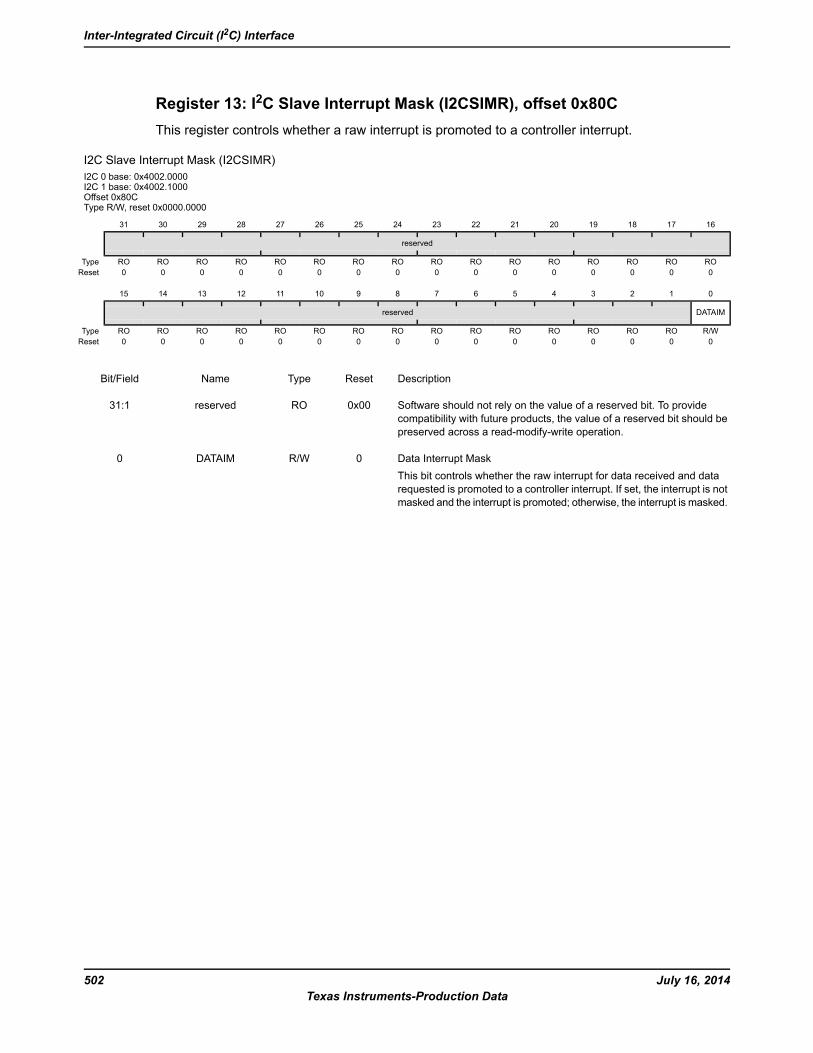
Register 13: I2C Slave Interrupt Mask (I2CSIMR), offset 0x80CThis register controls whether a raw interrupt is promoted to a controller interrupt.
I2C Slave Interrupt Mask (I2CSIMR)I2C 0 base: 0x4002.0000I2C 1 base: 0x4002.1000Offset 0x80CType R/W, reset 0x0000.0000
16171819202122232425262728293031
reserved
ROROROROROROROROROROROROROROROROType0000000000000000Reset
0123456789101112131415
DATAIMreserved
R/WROROROROROROROROROROROROROROROType0000000000000000Reset
DescriptionResetTypeNameBit/Field
Software should not rely on the value of a reserved bit. To providecompatibility with future products, the value of a reserved bit should bepreserved across a read-modify-write operation.
0x00ROreserved31:1
Data Interrupt MaskThis bit controls whether the raw interrupt for data received and datarequested is promoted to a controller interrupt. If set, the interrupt is notmasked and the interrupt is promoted; otherwise, the interrupt is masked.
0R/WDATAIM0
July 16, 2014502Texas Instruments-Production Data
Inter-Integrated Circuit (I2C) Interface
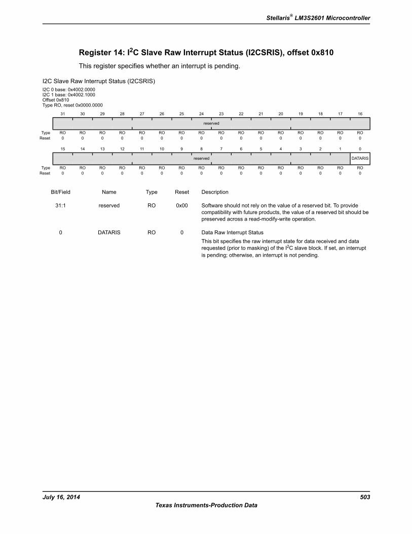
Register 14: I2C Slave Raw Interrupt Status (I2CSRIS), offset 0x810This register specifies whether an interrupt is pending.
I2C Slave Raw Interrupt Status (I2CSRIS)I2C 0 base: 0x4002.0000I2C 1 base: 0x4002.1000Offset 0x810Type RO, reset 0x0000.0000
16171819202122232425262728293031
reserved
ROROROROROROROROROROROROROROROROType0000000000000000Reset
0123456789101112131415
DATARISreserved
ROROROROROROROROROROROROROROROROType0000000000000000Reset
DescriptionResetTypeNameBit/Field
Software should not rely on the value of a reserved bit. To providecompatibility with future products, the value of a reserved bit should bepreserved across a read-modify-write operation.
0x00ROreserved31:1
Data Raw Interrupt StatusThis bit specifies the raw interrupt state for data received and datarequested (prior to masking) of the I2C slave block. If set, an interruptis pending; otherwise, an interrupt is not pending.
0RODATARIS0
503July 16, 2014Texas Instruments-Production Data
Stellaris® LM3S2601 Microcontroller
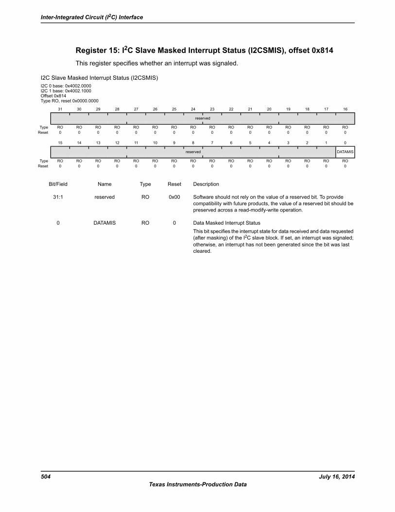
Register 15: I2C Slave Masked Interrupt Status (I2CSMIS), offset 0x814This register specifies whether an interrupt was signaled.
I2C Slave Masked Interrupt Status (I2CSMIS)I2C 0 base: 0x4002.0000I2C 1 base: 0x4002.1000Offset 0x814Type RO, reset 0x0000.0000
16171819202122232425262728293031
reserved
ROROROROROROROROROROROROROROROROType0000000000000000Reset
0123456789101112131415
DATAMISreserved
ROROROROROROROROROROROROROROROROType0000000000000000Reset
DescriptionResetTypeNameBit/Field
Software should not rely on the value of a reserved bit. To providecompatibility with future products, the value of a reserved bit should bepreserved across a read-modify-write operation.
0x00ROreserved31:1
Data Masked Interrupt StatusThis bit specifies the interrupt state for data received and data requested(after masking) of the I2C slave block. If set, an interrupt was signaled;otherwise, an interrupt has not been generated since the bit was lastcleared.
0RODATAMIS0
July 16, 2014504Texas Instruments-Production Data
Inter-Integrated Circuit (I2C) Interface
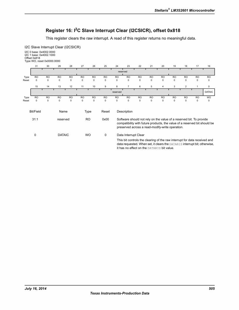
Register 16: I2C Slave Interrupt Clear (I2CSICR), offset 0x818This register clears the raw interrupt. A read of this register returns no meaningful data.
I2C Slave Interrupt Clear (I2CSICR)I2C 0 base: 0x4002.0000I2C 1 base: 0x4002.1000Offset 0x818Type WO, reset 0x0000.0000
16171819202122232425262728293031
reserved
ROROROROROROROROROROROROROROROROType0000000000000000Reset
0123456789101112131415
DATAICreserved
WOROROROROROROROROROROROROROROROType0000000000000000Reset
DescriptionResetTypeNameBit/Field
Software should not rely on the value of a reserved bit. To providecompatibility with future products, the value of a reserved bit should bepreserved across a read-modify-write operation.
0x00ROreserved31:1
Data Interrupt ClearThis bit controls the clearing of the raw interrupt for data received anddata requested. When set, it clears the DATARIS interrupt bit; otherwise,it has no effect on the DATARIS bit value.
0WODATAIC0
505July 16, 2014Texas Instruments-Production Data
Stellaris® LM3S2601 Microcontroller
14 Controller Area Network (CAN) ModuleController Area Network (CAN) is a multicast, shared serial bus standard for connecting electroniccontrol units (ECUs). CAN was specifically designed to be robust in electromagnetically-noisyenvironments and can utilize a differential balanced line like RS-485 or a more robust twisted-pairwire. Originally created for automotive purposes, it is also used in many embedded controlapplications (such as industrial and medical). Bit rates up to 1Mbps are possible at network lengthsless than 40 meters. Decreased bit rates allow longer network distances (for example, 125 Kbps at500 meters).
The Stellaris® CAN controller supports the following features:
CAN protocol version 2.0 part A/B
Bit rates up to 1 Mbps
32 message objects with individual identifier masks
Maskable interrupt
Disable Automatic Retransmission mode for Time-Triggered CAN (TTCAN) applications
Programmable Loopback mode for self-test operation
Programmable FIFO mode enables storage of multiple message objects
Gluelessly attaches to an external CAN interface through the CANnTX and CANnRX signals
July 16, 2014506Texas Instruments-Production Data
Controller Area Network (CAN) Module
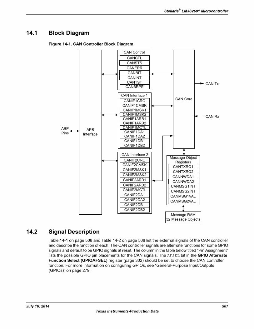
14.1 Block Diagram
Figure 14-1. CAN Controller Block Diagram
CAN Control
CAN Core
Message ObjectRegisters
CANNWDA2CANMSG1INTCANMSG2INTCANMSG1VALCANMSG2VAL
CAN TxCANINTCANTSTCANBRPE
CANBIT
APBInterface
ABPPins
Message RAM32 Message Objects
CANERR
CANCTLCANSTS
CANIF2ARB2CANIF2MCTLCANIF2DA1
CAN Interface 2
CANIF2DA2CANIF2DB1CANIF2DB2
CANIF2ARB1CANIF2MSK2
CANIF2CRQCANIF2CMSKCANIF2MSK1
CAN Interface 1CANIF1CRQCANIF1CMSKCANIF1MSK1CANIF1MSK2CANIF1ARB1CANIF1ARB2CANIF1MCTLCANIF1DA1CANIF1DA2CANIF1DB1CANIF1DB2
CAN Rx
CANNWDA1
CANTXRQ1CANTXRQ2
14.2 Signal DescriptionTable 14-1 on page 508 and Table 14-2 on page 508 list the external signals of the CAN controllerand describe the function of each. The CAN controller signals are alternate functions for someGPIOsignals and default to be GPIO signals at reset. The column in the table below titled "Pin Assignment"lists the possible GPIO pin placements for the CAN signals. The AFSEL bit in the GPIO AlternateFunction Select (GPIOAFSEL) register (page 302) should be set to choose the CAN controllerfunction. For more information on configuring GPIOs, see “General-Purpose Input/Outputs(GPIOs)” on page 279.
507July 16, 2014Texas Instruments-Production Data
Stellaris® LM3S2601 Microcontroller
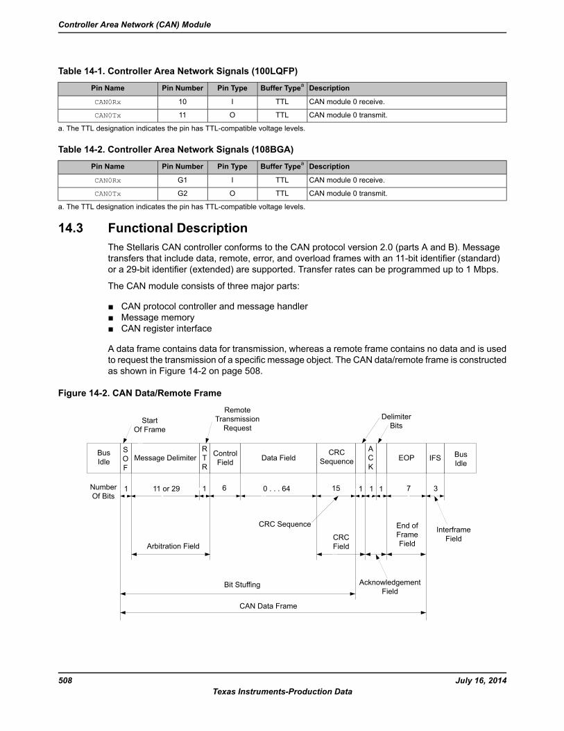
Table 14-1. Controller Area Network Signals (100LQFP)
DescriptionBuffer TypeaPin TypePin NumberPin Name
CAN module 0 receive.TTLI10CAN0Rx
CAN module 0 transmit.TTLO11CAN0Tx
a. The TTL designation indicates the pin has TTL-compatible voltage levels.
Table 14-2. Controller Area Network Signals (108BGA)
DescriptionBuffer TypeaPin TypePin NumberPin Name
CAN module 0 receive.TTLIG1CAN0Rx
CAN module 0 transmit.TTLOG2CAN0Tx
a. The TTL designation indicates the pin has TTL-compatible voltage levels.
14.3 Functional DescriptionThe Stellaris CAN controller conforms to the CAN protocol version 2.0 (parts A and B). Messagetransfers that include data, remote, error, and overload frames with an 11-bit identifier (standard)or a 29-bit identifier (extended) are supported. Transfer rates can be programmed up to 1 Mbps.
The CAN module consists of three major parts:
CAN protocol controller and message handler Message memory CAN register interface
A data frame contains data for transmission, whereas a remote frame contains no data and is usedto request the transmission of a specific message object. The CAN data/remote frame is constructedas shown in Figure 14-2 on page 508.
Figure 14-2. CAN Data/Remote Frame
NumberOf Bits
SOF
EOP IFS BusIdle
11 6111 or 29 0 . . . 64 15 7 31 1
ACK
Data FieldControlField
RTR
Message DelimiterBusIdle
Bit Stuffing
CAN Data Frame
Arbitration Field
CRC Sequence
CRCField
AcknowledgementField
End ofFrameField
InterframeField
StartOf Frame
RemoteTransmissionRequest
DelimiterBits
CRCSequence
July 16, 2014508Texas Instruments-Production Data
Controller Area Network (CAN) Module
The protocol controller transfers and receives the serial data from the CAN bus and passes the dataon to the message handler. The message handler then loads this information into the appropriatemessage object based on the current filtering and identifiers in the message object memory. Themessage handler is also responsible for generating interrupts based on events on the CAN bus.
Themessage object memory is a set of 32 identical memory blocks that hold the current configuration,status, and actual data for each message object. These are accessed via either of the CANmessageobject register interfaces.
The message memory is not directly accessible in the Stellaris memory map, so the Stellaris CANcontroller provides an interface to communicate with the message memory via two CAN interfaceregister sets for communicating with the message objects. As there is no direct access to themessage object memory, these two interfaces must be used to read or write to each message object.The two message object interfaces allow parallel access to the CAN controller message objectswhen multiple objects may have new information that must be processed. In general, one interfaceis used for transmit data and one for receive data.
14.3.1 InitializationSoftware initialization is started by setting the INIT bit in the CAN Control (CANCTL) register (withsoftware or by a hardware reset) or by going bus-off, which occurs when the transmitter's errorcounter exceeds a count of 255. While INIT is set, all message transfers to and from the CAN busare stopped and the CANnTX signal is held High. Entering the initialization state does not changethe configuration of the CAN controller, the message objects, or the error counters. However, someconfiguration registers are only accessible while in the initialization state.
To initialize the CAN controller, set the CAN Bit Timing (CANBIT) register and configure eachmessage object. If a message object is not needed, label it as not valid by clearing the MSGVAL bitin the CAN IFn Arbitration 2 (CANIFnARB2) register. Otherwise, the whole message object mustbe initialized, as the fields of the message object may not have valid information, causing unexpectedresults. Both the INIT and CCE bits in the CANCTL register must be set in order to access theCANBIT register and the CAN Baud Rate Prescaler Extension (CANBRPE) register to configurethe bit timing. To leave the initialization state, the INIT bit must be cleared. Afterwards, the internalBit Stream Processor (BSP) synchronizes itself to the data transfer on the CAN bus by waiting forthe occurrence of a sequence of 11 consecutive recessive bits (indicating a bus idle condition)before it takes part in bus activities and starts message transfers. Message object initialization doesnot require the CAN to be in the initialization state and can be done on the fly. However, messageobjects should all be configured to particular identifiers or set to not valid before message transferstarts. To change the configuration of a message object during normal operation, clear the MSGVALbit in the CANIFnARB2 register to indicate that the message object is not valid during the change.When the configuration is completed, set the MSGVAL bit again to indicate that the message objectis once again valid.
14.3.2 OperationThere are two sets of CAN Interface Registers (CANIF1x and CANIF2x), which are used to accessthe message objects in the Message RAM. The CAN controller coordinates transfers to and fromthe Message RAM to and from the registers. The two sets are independent and identical and canbe used to queue transactions. Generally, one interface is used to transmit data and one is used toreceive data.
Once the CAN module is initialized and the INIT bit in the CANCTL register is cleared, the CANmodule synchronizes itself to the CAN bus and starts the message transfer. As each message isreceived, it goes through the message handler's filtering process, and if it passes through the filter,is stored in the message object specified by the MNUM bit in the CAN IFn Command Request
509July 16, 2014Texas Instruments-Production Data
Stellaris® LM3S2601 Microcontroller
(CANIFnCRQ) register. The whole message (including all arbitration bits, data-length code, andeight data bytes) is stored in the message object. If the Identifier Mask (the MSK bits in the CAN IFnMask 1 andCAN IFnMask 2 (CANIFnMSKn) registers) is used, the arbitration bits that are maskedto "don't care" may be overwritten in the message object.
The CPUmay read or write eachmessage at any time via the CAN Interface Registers. Themessagehandler guarantees data consistency in case of concurrent accesses.
The transmission of message objects is under the control of the software that is managing the CANhardware. These can be message objects used for one-time data transfers, or permanent messageobjects used to respond in a more periodic manner. Permanent message objects have all arbitrationand control set up, and only the data bytes are updated. At the start of transmission, the appropriateTXRQST bit in the CAN Transmission Request n (CANTXRQn) register and the NEWDAT bit in theCAN New Data n (CANNWDAn) register are set. If several transmit messages are assigned to thesame message object (when the number of message objects is not sufficient), the whole messageobject has to be configured before the transmission of this message is requested.
The transmission of any number of message objects may be requested at the same time; they aretransmitted according to their internal priority, which is based on the message identifier (MNUM) forthe message object, with 1 being the highest priority and 32 being the lowest priority. Messagesmay be updated or set to not valid any time, even when their requested transmission is still pending.The old data is discarded when a message is updated before its pending transmission has started.Depending on the configuration of the message object, the transmission of a message may berequested autonomously by the reception of a remote frame with a matching identifier.
Transmission can be automatically started by the reception of a matching remote frame. To enablethis mode, set the RMTEN bit in theCAN IFnMessage Control (CANIFnMCTL) register. A matchingreceived remote frame causes the TXRQST bit to be set and the message object automaticallytransfers its data or generates an interrupt indicating a remote frame was requested. This can bestrictly a single message identifier, or it can be a range of values specified in the message object.The CANmask registers, CANIFnMSKn, configure which groups of frames are identified as remoteframe requests. The UMASK bit in the CANIFnMCTL register enables the MSK bits in theCANIFnMSKn register to filter which frames are identified as a remote frame request. The MXTDbit in the CANIFnMSK2 register should be set if a remote frame request is expected to be triggeredby 29-bit extended identifiers.
14.3.3 Transmitting Message ObjectsIf the internal transmit shift register of the CAN module is ready for loading, and if there is no datatransfer occurring between the CAN Interface Registers and message RAM, the valid messageobject with the highest priority that has a pending transmission request is loaded into the transmitshift register by the message handler and the transmission is started. The message object's NEWDATbit in the CANNWDAn register is cleared. After a successful transmission, and if no new data waswritten to the message object since the start of the transmission, the TXRQST bit in the CANTXRQnregister is cleared. If the CAN controller is set up to interrupt upon a successful transmission of amessage object, (the TXIE bit in the CAN IFn Message Control (CANIFnMCTL) register is set),the INTPND bit in the CANIFnMCTL register is set after a successful transmission. If the CANmodule has lost the arbitration or if an error occurred during the transmission, the message isre-transmitted as soon as the CAN bus is free again. If, meanwhile, the transmission of a messagewith higher priority has been requested, the messages are transmitted in the order of their priority.
14.3.4 Configuring a Transmit Message ObjectThe following steps illustrate how to configure a transmit message object.
July 16, 2014510Texas Instruments-Production Data
Controller Area Network (CAN) Module
1. In the CAN IFn Command Mask (CANIFnCMASK) register:
Set the WRNRD bit to specify a write to the CANIFnCMASK register; specify whether totransfer the IDMASK, DIR, and MXTD of the message object into the CAN IFn registers usingthe MASK bit
Specify whether to transfer the ID, DIR, XTD, and MSGVAL of the message object into theinterface registers using the ARB bit
Specify whether to transfer the control bits into the interface registers using the CONTROLbit
Specify whether to clear the INTPND bit in the CANIFnMCTL register using the CLRINTPNDbit
Specify whether to clear the NEWDAT bit in the CANNWDAn register using the NEWDAT bit
Specify which bits to transfer using the DATAA and DATAB bits
2. In the CANIFnMSK1 register, use the MSK[15:0] bits to specify which of the bits in the 29-bitor 11-bit message identifier are used for acceptance filtering. Note that MSK[15:0] in thisregister are used for bits [15:0] of the 29-bit message identifier and are not used for an 11-bitidentifier. A value of 0x00 enables all messages to pass through the acceptance filtering. Alsonote that in order for these bits to be used for acceptance filtering, they must be enabled bysetting the UMASK bit in the CANIFnMCTL register.
3. In the CANIFnMSK2 register, use the MSK[12:0] bits to specify which of the bits in the 29-bitor 11-bit message identifier are used for acceptance filtering. Note that MSK[12:0] are usedfor bits [28:16] of the 29-bit message identifier; whereas MSK[12:2] are used for bits [10:0] ofthe 11-bit message identifier. Use the MXTD and MDIR bits to specify whether to use XTD andDIR for acceptance filtering. A value of 0x00 enables all messages to pass through theacceptance filtering. Also note that in order for these bits to be used for acceptance filtering,they must be enabled by setting the UMASK bit in the CANIFnMCTL register.
4. For a 29-bit identifier, configure ID[15:0] in the CANIFnARB1 register to are used for bits[15:0] of the message identifier and ID[12:0] in the CANIFnARB2 register to are used forbits [28:16] of the message identifier. Set the XTD bit to indicate an extended identifier; set theDIR bit to indicate transmit; and set the MSGVAL bit to indicate that the message object is valid.
5. For an 11-bit identifier, disregard the CANIFnARB1 register and configure ID[12:2] in theCANIFnARB2 register to are used for bits [10:0] of the message identifier. Clear the XTD bit toindicate a standard identifier; set the DIR bit to indicate transmit; and set the MSGVAL bit toindicate that the message object is valid.
6. In the CANIFnMCTL register:
Optionally set the UMASK bit to enable the mask (MSK, MXTD, and MDIR specified in theCANIFnMSK1 and CANIFnMSK2 registers) for acceptance filtering
Optionally set the TXIE bit to enable the INTPND bit to be set after a successful transmission
Optionally set the RMTEN bit to enable the TXRQST bit to be set upon the reception of amatching remote frame allowing automatic transmission
511July 16, 2014Texas Instruments-Production Data
Stellaris® LM3S2601 Microcontroller
Set the EOB bit for a single message object;
Set the DLC[3:0] field to specify the size of the data frame. Take care during thisconfiguration not to set the NEWDAT, MSGLST, INTPND or TXRQST bits.
7. Load the data to be transmitted into the CAN IFn Data (CANIFnDA1, CANIFnDA2, CANIFnDB1,CANIFnDB2) or (CANIFnDATAA and CANIFnDATAB) registers. Byte 0 of the CAN data frameis stored in DATA[7:0] in the CANIFnDA1 register.
8. Program the number of the message object to be transmitted in the MNUM field in the CAN IFnCommand Request (CANIFnCRQ) register.
9. When everything is properly configured, set the TXRQST bit in the CANIFnMCTL register. Oncethis bit is set, the message object is available to be transmitted, depending on priority and busavailability. Note that setting the RMTEN bit in theCANIFnMCTL register can also start messagetransmission if a matching remote frame has been received.
14.3.5 Updating a Transmit Message ObjectThe CPU may update the data bytes of a Transmit Message Object any time via the CAN InterfaceRegisters and neither the MSGVAL bit in the CANIFnARB2 register nor the TXRQST bits in theCANIFnMCTL register have to be cleared before the update.
Even if only some of the data bytes are to be updated, all four bytes of the correspondingCANIFnDAn/CANIFnDBn register have to be valid before the content of that register is transferredto the message object. Either the CPU must write all four bytes into the CANIFnDAn/CANIFnDBnregister or the message object is transferred to the CANIFnDAn/CANIFnDBn register before theCPU writes the new data bytes.
In order to only update the data in a message object, the WRNRD, DATAA and DATAB bits in theCANIFnMSKn register are set, followed by writing the updated data intoCANIFnDA1,CANIFnDA2,CANIFnDB1, and CANIFnDB2 registers, and then the number of the message object is written tothe MNUM field in the CAN IFn Command Request (CANIFnCRQ) register. To begin transmissionof the new data as soon as possible, set the TXRQST bit in the CANIFnMSKn register.
To prevent the clearing of the TXRQST bit in the CANIFnMCTL register at the end of a transmissionthat may already be in progress while the data is updated, the NEWDAT and TXRQST bits have to beset at the same time in theCANIFnMCTL register. When these bits are set at the same time, NEWDATis cleared as soon as the new transmission has started.
14.3.6 Accepting Received Message ObjectsWhen the arbitration and control field (the ID and XTD bits in the CANIFnARB2 and the RMTEN andDLC[3:0] bits of the CANIFnMCTL register) of an incoming message is completely shifted intothe CAN controller, the message handling capability of the controller starts scanning the messageRAM for a matching valid message object. To scan the message RAM for a matching messageobject, the controller uses the acceptance filtering programmed through the mask bits in theCANIFnMSKn register and enabled using the UMASK bit in the CANIFnMCTL register. Each validmessage object, starting with object 1, is compared with the incoming message to locate a matchingmessage object in the message RAM. If a match occurs, the scanning is stopped and the messagehandler proceeds depending on whether it is a data frame or remote frame that was received.
14.3.7 Receiving a Data FrameThe message handler stores the message from the CAN controller receive shift register into thematching message object in the message RAM. The data bytes, all arbitration bits, and the DLC bits
July 16, 2014512Texas Instruments-Production Data
Controller Area Network (CAN) Module
are all stored into the corresponding message object. In this manner, the data bytes are connectedwith the identifier even if arbitration masks are used. The NEWDAT bit of the CANIFnMCTL registeris set to indicate that new data has been received. The CPU should clear this bit when it reads themessage object to indicate to the controller that the message has been received, and the buffer isfree to receive more messages. If the CAN controller receives a message and the NEWDAT bit isalready set, the MSGLST bit in the CANIFnMCTL register is set to indicate that the previous datawas lost. If the system requires an interrupt upon successful reception of a frame, the RXIE bit ofthe CANIFnMCTL register should be set. In this case, the INTPND bit of the same register is set,causing the CANINT register to point to the message object that just received a message. TheTXRQST bit of this message object should be cleared to prevent the transmission of a remote frame.
14.3.8 Receiving a Remote FrameA remote frame contains no data, but instead specifies which object should be transmitted. Whena remote frame is received, three different configurations of the matching message object have tobe considered:
DescriptionConfiguration in CANIFnMCTL
At the reception of a matching remote frame, the TXRQST bit of thismessage object is set. The rest of the message object remainsunchanged, and the controller automatically transfers the data inthe message object as soon as possible.
DIR = 1 (direction = transmit); programmed in theCANIFnARB2 register
RMTEN = 1 (set the TXRQST bit of theCANIFnMCTL register at reception of the frameto enable transmission)
UMASK = 1 or 0
At the reception of a matching remote frame, the TXRQST bit of thismessage object remains unchanged, and the remote frame isignored. This remote frame is disabled, the data is not transferredand there is no indication that the remote frame ever happened.
DIR = 1 (direction = transmit); programmed in theCANIFnARB2 register
RMTEN = 0 (do not change the TXRQST bit of theCANIFnMCTL register at reception of the frame)
UMASK = 0 (ignore mask in the CANIFnMSKnregister)
At the reception of a matching remote frame, the TXRQST bit of thismessage object is cleared. The arbitration and control field (ID +XTD + RMTEN + DLC) from the shift register is stored into themessage object in the message RAM and the NEWDAT bit of thismessage object is set. The data field of the message object remainsunchanged; the remote frame is treated similar to a received dataframe. This is useful for a remote data request from another CANdevice for which the Stellaris controller does not have readilyavailable data. The software must fill the data and answer the framemanually.
DIR = 1 (direction = transmit); programmed in theCANIFnARB2 register
RMTEN = 0 (do not change the TXRQST bit of theCANIFnMCTL register at reception of the frame)
UMASK = 1 (use mask (MSK, MXTD, and MDIR intheCANIFnMSKn register) for acceptance filtering)
14.3.9 Receive/Transmit PriorityThe receive/transmit priority for the message objects is controlled by the message number. Messageobject 1 has the highest priority, while message object 32 has the lowest priority. If more than onetransmission request is pending, the message objects are transmitted in order based on the messageobject with the lowest message number. This should not be confused with the message identifieras that priority is enforced by the CAN bus. This means that if message object 1 andmessage object2 both have valid messages that need to be transmitted, message object 1 will always be transmittedfirst regardless of the message identifier in the message object itself.
513July 16, 2014Texas Instruments-Production Data
Stellaris® LM3S2601 Microcontroller
14.3.10 Configuring a Receive Message ObjectThe following steps illustrate how to configure a receive message object.
1. Program the CAN IFn Command Mask (CANIFnCMASK) register as described in the“Configuring a Transmit Message Object” on page 510 section, except that the WRNRD bit is setto specify a write to the message RAM.
2. Program the CANIFnMSK1and CANIFnMSK2 registers as described in the “Configuring aTransmit Message Object” on page 510 section to configure which bits are used for acceptancefiltering. Note that in order for these bits to be used for acceptance filtering, they must be enabledby setting the UMASK bit in the CANIFnMCTL register.
3. In the CANIFnMSK2 register, use the MSK[12:0] bits to specify which of the bits in the 29-bitor 11-bit message identifier are used for acceptance filtering. Note that MSK[12:0] are usedfor bits [28:16] of the 29-bit message identifier; whereas MSK[12:2] are used for bits [10:0] ofthe 11-bit message identifier. Use the MXTD and MDIR bits to specify whether to use XTD andDIR for acceptance filtering. A value of 0x00 enables all messages to pass through theacceptance filtering. Also note that in order for these bits to be used for acceptance filtering,they must be enabled by setting the UMASK bit in the CANIFnMCTL register.
4. Program the CANIFnARB1 and CANIFnARB2 registers as described in the “Configuring aTransmit Message Object” on page 510 section to program XTD and ID bits for the messageidentifier to be received; set the MSGVAL bit to indicate a valid message; and clear the DIR bitto specify receive.
5. In the CANIFnMCTL register:
Optionally set the UMASK bit to enable the mask (MSK, MXTD, and MDIR specified in theCANIFnMSK1 and CANIFnMSK2 registers) for acceptance filtering
Optionally set the RXIE bit to enable the INTPND bit to be set after a successful reception
Clear the RMTEN bit to leave the TXRQST bit unchanged
Set the EOB bit for a single message object
Set the DLC[3:0] field to specify the size of the data frame
Take care during this configuration not to set the NEWDAT, MSGLST, INTPND or TXRQST bits.
6. Program the number of the message object to be received in the MNUM field in the CAN IFnCommand Request (CANIFnCRQ) register. Reception of the message object begins as soonas a matching frame is available on the CAN bus.
When the message handler stores a data frame in the message object, it stores the received DataLength Code and eight data bytes in theCANIFnDA1,CANIFnDA2,CANIFnDB1, andCANIFnDB2register. Byte 0 of the CAN data frame is stored in DATA[7:0] in the CANIFnDA1 register. If theData Length Code is less than 8, the remaining bytes of the message object are overwritten byunspecified values.
The CAN mask registers can be used to allow groups of data frames to be received by a messageobject. The CAN mask registers, CANIFnMSKn, configure which groups of frames are received bya message object. The UMASK bit in the CANIFnMCTL register enables the MSK bits in the
July 16, 2014514Texas Instruments-Production Data
Controller Area Network (CAN) Module
CANIFnMSKn register to filter which frames are received. The MXTD bit in theCANIFnMSK2 registershould be set if only 29-bit extended identifiers are expected by this message object.
14.3.11 Handling of Received Message ObjectsThe CPU may read a received message any time via the CAN Interface registers because the dataconsistency is guaranteed by the message handler state machine.
Typically, the CPU first writes 0x007F to the CANIFnCMSK register and then writes the number ofthe message object to the CANIFnCRQ register. That combination transfers the whole receivedmessage from the message RAM into the Message Buffer registers (CANIFnMSKn,CANIFnARBn,and CANIFnMCTL). Additionally, the NEWDAT and INTPND bits are cleared in the message RAM,acknowledging that the message has been read and clearing the pending interrupt generated bythis message object.
If the message object uses masks for acceptance filtering, the CANIFnARBn registers show thefull, unmasked ID for the received message.
The NEWDAT bit in the CANIFnMCTL register shows whether a new message has been receivedsince the last time this message object was read. The MSGLST bit in the CANIFnMCTL registershows whether more than one message has been received since the last time this message objectwas read. MSGLST is not automatically cleared, and should be cleared by software after reading itsstatus.
Using a remote frame, the CPU may request new data from another CAN node on the CAN bus.Setting the TXRQST bit of a receive object causes the transmission of a remote frame with the receiveobject's identifier. This remote frame triggers the other CAN node to start the transmission of thematching data frame. If the matching data frame is received before the remote frame could betransmitted, the TXRQST bit is automatically reset. This prevents the possible loss of data when theother device on the CAN bus has already transmitted the data slightly earlier than expected.
14.3.11.1 Configuration of a FIFO BufferWith the exception of the EOB bit in theCANIFnMCTL register, the configuration of receive messageobjects belonging to a FIFO buffer is the same as the configuration of a single receive messageobject (see “Configuring a Receive Message Object” on page 514). To concatenate two or moremessage objects into a FIFO buffer, the identifiers and masks (if used) of these message objectshave to be programmed to matching values. Due to the implicit priority of the message objects, themessage object with the lowest message object number is the first message object in a FIFO buffer.The EOB bit of all message objects of a FIFO buffer except the last one must be cleared. The EOBbit of the last message object of a FIFO buffer is set, indicating it is the last entry in the buffer.
14.3.11.2 Reception of Messages with FIFO BuffersReceived messages with identifiers matching to a FIFO buffer are stored starting with the messageobject with the lowest message number. When a message is stored into a message object of aFIFO buffer, the NEWDAT of the CANIFnMCTL register bit of this message object is set. By settingNEWDAT while EOB is clear, the message object is locked and cannot be written to by the messagehandler until the CPU has cleared the NEWDAT bit. Messages are stored into a FIFO buffer until thelast message object of this FIFO buffer is reached. If none of the preceding message objects hasbeen released by clearing the NEWDAT bit, all further messages for this FIFO buffer will be writteninto the last message object of the FIFO buffer and therefore overwrite previous messages.
515July 16, 2014Texas Instruments-Production Data
Stellaris® LM3S2601 Microcontroller
14.3.11.3 Reading from a FIFO BufferWhen the CPU transfers the contents of a message object from a FIFO buffer by writing its numberto the CANIFnCRQ, the TXRQST and CLRINTPND bits in the CANIFnCMSK register should be setsuch that the NEWDAT and INTPEND bits in the CANIFnMCTL register are cleared after the read.The values of these bits in the CANIFnMCTL register always reflect the status of the messageobject before the bits are cleared. To assure the correct function of a FIFO buffer, the CPU shouldread out the message objects starting with the message object with the lowest message number.When reading from the FIFO buffer, the user should be aware that a new received message isplaced in the message object with the lowest message number for which the NEWDAT bit of theCANIFnMCTL register. As a result, the order of the receivedmessages in the FIFO is not guaranteed.Figure 14-3 on page 517 shows how a set of message objects which are concatenated to a FIFOBuffer can be handled by the CPU.
July 16, 2014516Texas Instruments-Production Data
Controller Area Network (CAN) Module
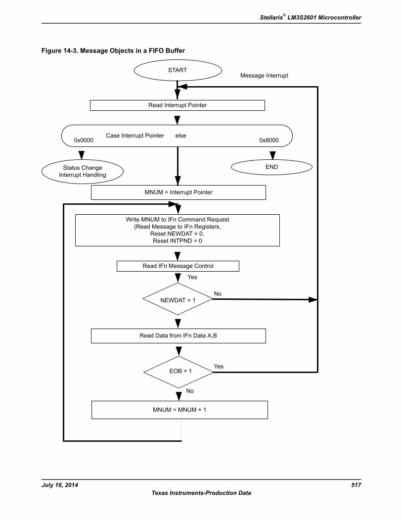
Figure 14-3. Message Objects in a FIFO Buffer
START
No
Yes
Write MNUM to IFn Command Request(Read Message to IFn Registers,
Reset NEWDAT = 0,Reset INTPND = 0
MNUM = Interrupt Pointer
Read IFn Message Control
Read Data from IFn Data A,B
NEWDAT = 1
EOB = 1
Read Interrupt Pointer
Status ChangeInterrupt Handling
END
Message Interrupt
Yes
MNUM = MNUM + 1
Case Interrupt Pointer else0x0000 0x8000
No
517July 16, 2014Texas Instruments-Production Data
Stellaris® LM3S2601 Microcontroller
14.3.12 Handling of InterruptsIf several interrupts are pending, theCAN Interrupt (CANINT) register points to the pending interruptwith the highest priority, disregarding their chronological order. The status interrupt has the highestpriority. Among the message interrupts, the message object's interrupt with the lowest messagenumber has the highest priority. A message interrupt is cleared by clearing the message object'sINTPND bit in the CANIFnMCTL register or by reading the CAN Status (CANSTS) register. Thestatus Interrupt is cleared by reading the CANSTS register.
The interrupt identifier INTID in the CANINT register indicates the cause of the interrupt. When nointerrupt is pending, the register reads as 0x0000. If the value of the INTID field is different from 0,then there is an interrupt pending. If the IE bit is set in the CANCTL register, the interrupt line tothe CPU is active. The interrupt line remains active until the INTID field is 0, meaning that all interruptsources have been cleared (the cause of the interrupt is reset), or until IE is cleared, which disablesinterrupts from the CAN controller.
The INTID field of the CANINT register points to the pending message interrupt with the highestinterrupt priority. The SIE bit in the CANCTL register controls whether a change of the RXOK, TXOK,and LEC bits in the CANSTS register can cause an interrupt. The EIE bit in the CANCTLregistercontrols whether a change of the BOFF and EWARN bits in the CANSTS can cause an interrupt. TheIE bit in the CANCTL controls whether any interrupt from the CAN controller actually generates aninterrupt to the microcontroller's interrupt controller. The CANINT register is updated even whenthe IE bit in the CANCTL register is clear, but the interrupt will not be indicated to the CPU.
A value of 0x8000 in the CANINT register indicates that an interrupt is pending because the CANmodule has updated, but not necessarily changed, the CANSTS , indicating that either an error orstatus interrupt has been generated. A write access to the CANSTS register can clear the RXOK,TXOK, and LEC bits in that same register; however, the only way to clear the source of a statusinterrupt is to read the CANSTS register.
There are two ways to determine the source of an interrupt during interrupt handling. The first is toread the INTID bit in the CANINT register to determine the highest priority interrupt that is pending,and the second is to read the CAN Message Interrupt Pending (CANMSGnINT) register to seeall of the message objects that have pending interrupts.
An interrupt service routine reading the message that is the source of the interrupt may read themessage and clear the message object's INTPND bit at the same time by setting the CLRINTPNDbit in the CANIFnCMSK register. Once the INTPND bit has been cleared, the CANINT registercontains the message number for the next message object with a pending interrupt.
14.3.13 Test ModeA Test Mode is provided, which allows various diagnostics to be performed. Test Mode is enteredby setting the TEST bit CANCTL register. Once in Test Mode, the TX[1:0], LBACK, SILENT andBASIC bits in the CAN Test (CANTST) register can be used to put the CAN controller into thevarious diagnostic modes. The RX bit in the CANTST register allows monitoring of the CANnRXsignal. All CANTST register functions are disabled when the TEST bit is cleared.
14.3.13.1 Silent ModeSilent Mode can be used to analyze the traffic on a CAN bus without affecting it by the transmissionof dominant bits (Acknowledge Bits, Error Frames). The CAN Controller is put in Silent Mode settingthe SILENT bit in the CANTST register. In Silent Mode, the CAN controller is able to receive validdata frames and valid remote frames, but it sends only recessive bits on the CAN bus and it cannotstart a transmission. If the CAN Controller is required to send a dominant bit (ACK bit, overload flag,
July 16, 2014518Texas Instruments-Production Data
Controller Area Network (CAN) Module
or active error flag), the bit is rerouted internally so that the CAN Controller monitors this dominantbit, although the CAN bus remains in recessive state.
14.3.13.2 Loopback ModeLoopback mode is useful for self-test functions. In Loopback Mode, the CAN Controller internallyroutes the CANnTX signal on to the CANnRX signal and treats its own transmitted messages asreceived messages and stores them (if they pass acceptance filtering) into the message buffer. TheCAN Controller is put in Loopback Mode by setting the LBACK bit in the CANTST register. To beindependent from external stimulation, the CAN Controller ignores acknowledge errors (a recessivebit sampled in the acknowledge slot of a data/remote frame) in Loopback Mode. The actual valueof the CANnRX signal is disregarded by the CAN Controller. The transmitted messages can bemonitored on the CANnTX signal.
14.3.13.3 Loopback Combined with Silent ModeLoopback Mode and Silent Mode can be combined to allow the CAN Controller to be tested withoutaffecting a running CAN system connected to the CANnTX and CANnRX signals. In this mode, theCANnRX signal is disconnected from the CAN Controller and the CANnTX signal is held recessive.This mode is enabled by setting both the LBACK and SILENT bits in the CANTST register.
14.3.13.4 Basic ModeBasic Mode allows the CAN Controller to be operated without the Message RAM. In Basic Mode,The CANIF1 registers are used as the transmit buffer. The transmission of the contents of the IF1registers is requested by setting the BUSY bit of the CANIF1CRQ register. The CANIF1 registersare locked while the BUSY bit is set. The BUSY bit indicates that a transmission is pending. As soonthe CAN bus is idle, the CANIF1 registers are loaded into the shift register of the CAN Controllerand transmission is started. When the transmission has completed, the BUSY bit is cleared and thelocked CANIF1 registers are released. A pending transmission can be aborted at any time by clearingthe BUSY bit in the CANIF1CRQ register while the CANIF1 registers are locked. If the CPU hascleared the BUSY bit, a possible retransmission in case of lost arbitration or an error is disabled.
The CANIF2 Registers are used as a receive buffer. After the reception of a message, the contentsof the shift register is stored into the CANIF2 registers, without any acceptance filtering. Additionally,the actual contents of the shift register can be monitored during the message transfer. Each time aread message object is initiated by setting the BUSY bit of the CANIF2CRQ register, the contentsof the shift register are stored into the CANIF2 registers.
In Basic Mode, all message-object-related control and status bits and of the control bits of theCANIFnCMSK registers are not evaluated. The message number of the CANIFnCRQ registers isalso not evaluated. In the CANIF2MCTL register, the NEWDAT and MSGLST bits retain their function,the DLC[3:0] field shows the received DLC, the other control bits are cleared.
Basic Mode is enabled by setting the BASIC bit in the CANTST register.
14.3.13.5 Transmit ControlSoftware can directly override control of the CANnTX signal in four different ways.
CANnTX is controlled by the CAN Controller
The sample point is driven on the CANnTX signal to monitor the bit timing
CANnTX drives a low value
519July 16, 2014Texas Instruments-Production Data
Stellaris® LM3S2601 Microcontroller
CANnTX drives a high value
The last two functions, combined with the readable CAN receive pin CANnRX, can be used to checkthe physical layer of the CAN bus.
The Transmit Control function is enabled by programming the TX[1:0] field in theCANTST register.The three test functions for the CANnTX signal interfere with all CAN protocol functions. TX[1:0]must be cleared when CAN message transfer or Loopback Mode, Silent Mode, or Basic Mode areselected.
14.3.14 Bit Timing Configuration Error ConsiderationsEven if minor errors in the configuration of the CAN bit timing do not result in immediate failure, theperformance of a CAN network can be reduced significantly. In many cases, the CAN bitsynchronization amends a faulty configuration of the CAN bit timing to such a degree that onlyoccasionally an error frame is generated. In the case of arbitration, however, when two or moreCAN nodes simultaneously try to transmit a frame, a misplaced sample point may cause one of thetransmitters to become error passive. The analysis of such sporadic errors requires a detailedknowledge of the CAN bit synchronization inside a CAN node and of the CAN nodes' interaction onthe CAN bus.
14.3.15 Bit Time and Bit RateThe CAN system supports bit rates in the range of lower than 1 Kbps up to 1000 Kbps. Each memberof the CAN network has its own clock generator. The timing parameter of the bit time can beconfigured individually for each CAN node, creating a common bit rate even though the CAN nodes'oscillator periods may be different.
Because of small variations in frequency caused by changes in temperature or voltage and bydeteriorating components, these oscillators are not absolutely stable. As long as the variationsremain inside a specific oscillator's tolerance range, the CAN nodes are able to compensate for thedifferent bit rates by periodically resynchronizing to the bit stream.
According to the CAN specification, the bit time is divided into four segments (see Figure14-4 on page 521): the Synchronization Segment, the Propagation Time Segment, the Phase BufferSegment 1, and the Phase Buffer Segment 2. Each segment consists of a specific, programmablenumber of time quanta (see Table 14-3 on page 521). The length of the time quantum (tq), which isthe basic time unit of the bit time, is defined by the CAN controller's input clock (fsys) and the BaudRate Prescaler (BRP):
tq = BRP / fsys
The fsys input clock is 8 MHz.
The Synchronization Segment Sync is that part of the bit time where edges of the CAN bus levelare expected to occur; the distance between an edge that occurs outside of Sync and the Sync iscalled the phase error of that edge.
The Propagation Time Segment Prop is intended to compensate for the physical delay times withinthe CAN network.
The Phase Buffer Segments Phase1 and Phase2 surround the Sample Point.
The (Re-)Synchronization Jump Width (SJW) defines how far a resynchronization may move theSample Point inside the limits defined by the Phase Buffer Segments to compensate for edge phaseerrors.
July 16, 2014520Texas Instruments-Production Data
Controller Area Network (CAN) Module
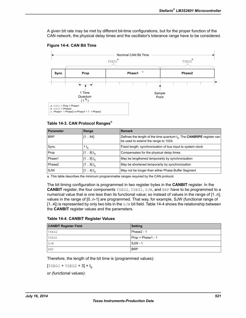
A given bit rate may be met by different bit-time configurations, but for the proper function of theCAN network, the physical delay times and the oscillator's tolerance range have to be considered.
Figure 14-4. CAN Bit Time
Sync Prop Phase2
SamplePoint
1 TimeQuantum( t q )q
Nominal CAN Bit Time
a. TSEG1 = Prop + Phase1b. TSEG2 = Phase2c. Phase1 = Phase2 or Phase1 + 1 = Phase2
TSEG1a
TSEG2b
Phase1 c
Table 14-3. CAN Protocol Rangesa
RemarkRangeParameter
Defines the length of the time quantum tq. The CANBRPE register canbe used to extend the range to 1024.
[1 .. 64]BRP
Fixed length, synchronization of bus input to system clock1 tqSync
Compensates for the physical delay times[1 .. 8] tqProp
May be lengthened temporarily by synchronization[1 .. 8] tqPhase1
May be shortened temporarily by synchronization[1 .. 8] tqPhase2
May not be longer than either Phase Buffer Segment[1 .. 4] tqSJW
a. This table describes the minimum programmable ranges required by the CAN protocol.
The bit timing configuration is programmed in two register bytes in the CANBIT register. In theCANBIT register, the four components TSEG2, TSEG1, SJW, and BRP have to be programmed to anumerical value that is one less than its functional value; so instead of values in the range of [1..n],values in the range of [0..n-1] are programmed. That way, for example, SJW (functional range of[1..4]) is represented by only two bits in the SJW bit field. Table 14-4 shows the relationship betweenthe CANBIT register values and the parameters.
Table 14-4. CANBIT Register Values
SettingCANBIT Register Field
Phase2 - 1TSEG2
Prop + Phase1 - 1TSEG1
SJW - 1SJW
BRPBRP
Therefore, the length of the bit time is (programmed values):
[TSEG1 + TSEG2 + 3] × tqor (functional values):
521July 16, 2014Texas Instruments-Production Data
Stellaris® LM3S2601 Microcontroller
[Sync + Prop + Phase1 + Phase2] × tqThe data in the CANBIT register is the configuration input of the CAN protocol controller. The baudrate prescaler (configured by the BRP field) defines the length of the time quantum, the basic timeunit of the bit time; the bit timing logic (configured by TSEG1, TSEG2, and SJW) defines the numberof time quanta in the bit time.
The processing of the bit time, the calculation of the position of the sample point, and occasionalsynchronizations are controlled by the CAN controller and are evaluated once per time quantum.
The CAN controller translates messages to and from frames. In addition, the controller generatesand discards the enclosing fixed format bits, inserts and extracts stuff bits, calculates and checksthe CRC code, performs the error management, and decides which type of synchronization is to beused. The bit value is received or transmitted at the sample point. The information processing time(IPT) is the time after the sample point needed to calculate the next bit to be transmitted on the CANbus. The IPT includes any of the following: retrieving the next data bit, handling a CRC bit, determiningif bit stuffing is required, generating an error flag or simply going idle.
The IPT is application-specific but may not be longer than 2 tq; the CAN's IPT is 0 tq. Its length isthe lower limit of the programmed length of Phase2. In case of synchronization, Phase2 may beshortened to a value less than IPT, which does not affect bus timing.
14.3.16 Calculating the Bit Timing ParametersUsually, the calculation of the bit timing configuration starts with a required bit rate or bit time. Theresulting bit time (1/bit rate) must be an integer multiple of the system clock period.
The bit time may consist of 4 to 25 time quanta. Several combinations may lead to the required bittime, allowing iterations of the following steps.
The first part of the bit time to be defined is Prop. Its length depends on the delay times measuredin the system. A maximum bus length as well as a maximum node delay has to be defined forexpandable CAN bus systems. The resulting time for Prop is converted into time quanta (roundedup to the nearest integer multiple of tq).
Sync is 1 tq long (fixed), which leaves (bit time - Prop - 1) tq for the two Phase Buffer Segments. Ifthe number of remaining tq is even, the Phase Buffer Segments have the same length, that is,Phase2 = Phase1, else Phase2 = Phase1 + 1.
The minimum nominal length of Phase2 has to be regarded as well. Phase2 may not be shorterthan the CAN controller's Information Processing Time, which is, depending on the actualimplementation, in the range of [0..2] tq.
The length of the synchronization jump width is set to the least of 4, Phase1 or Phase2.
The oscillator tolerance range necessary for the resulting configuration is calculated by the formulagiven below:
( ) ( ) fnomdffoscfnomdf ×+≤≤×− 11
( )( )2_132
min2_,1_SegPhasetbit
segPhasesegPhasedf
−××≤
fnomdfdf ××= 2max
where:
df = Maximum tolerance of oscillator frequency
fosc = Actual oscillator frequency
July 16, 2014522Texas Instruments-Production Data
Controller Area Network (CAN) Module
fnom = Nominal oscillator frequency
Maximum frequency tolerance must take into account the following formulas:( ) ( ) fnomdffoscfnomdf ×+≤≤×− 11
( )( )2_132
min2_,1_SegPhasetbit
segPhasesegPhasedf
−××≤
fnomdfdf ××= 2max
( ) ( ) fnomdffoscfnomdf ×+≤≤×− 11
( )( )2_132
min2_,1_SegPhasetbit
segPhasesegPhasedf
−××≤
fnomdfdf ××= 2max
where:
Phase1 and Phase2 are from Table 14-3 on page 521
tbit = Bit Time
dfmax = Maximum difference between two oscillators
If more than one configuration is possible, that configuration allowing the highest oscillator tolerancerange should be chosen.
CAN nodes with different system clocks require different configurations to come to the same bitrate. The calculation of the propagation time in the CAN network, based on the nodes with thelongest delay times, is done once for the whole network.
The CAN system's oscillator tolerance range is limited by the node with the lowest tolerance range.
The calculation may show that bus length or bit rate have to be decreased or that the oscillatorfrequencies' stability has to be increased in order to find a protocol-compliant configuration of theCAN bit timing.
14.3.16.1 Example for Bit Timing at High Baud RateIn this example, the frequency of CAN clock is 8 MHz, and the bit rate is 1 Mbps.
bit time = 1 µs = n * tq = 8 * tqtq = 125 nstq = (Baud rate Prescaler)/CAN ClockBaud rate Prescaler = tq * CAN ClockBaud rate Prescaler = 125E-9 * 8E6 = 1
tSync = 1 * tq = 125 ns \\fixed at 1 time quanta
delay of bus driver 50 nsdelay of receiver circuit 30 nsdelay of bus line (40m) 220 nstProp 375 ns = 3 * tq \\375 is next integer multiple of tq
bit time = tSync + tTSeg1 + tTSeg2 = 8 * tqbit time = tSync + tProp + tPhase 1 + tPhase2tPhase 1 + tPhase2 = bit time - tSync - tProp tPhase 1 + tPhase2 = (8 * tq) - (1 * tq) - (3 * tq) tPhase 1 + tPhase2 = 4 * tq
523July 16, 2014Texas Instruments-Production Data
Stellaris® LM3S2601 Microcontroller
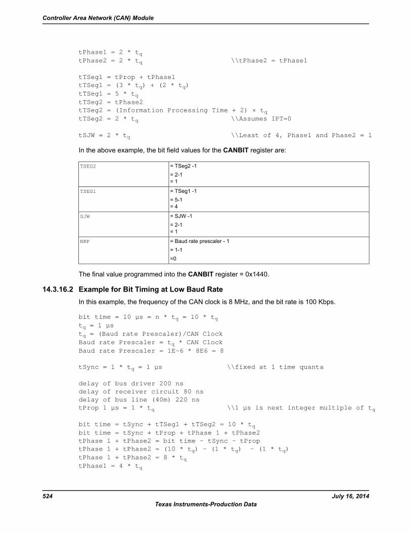
tPhase1 = 2 * tqtPhase2 = 2 * tq \\tPhase2 = tPhase1
tTSeg1 = tProp + tPhase1 tTSeg1 = (3 * tq) + (2 * tq) tTSeg1 = 5 * tqtTSeg2 = tPhase2 tTSeg2 = (Information Processing Time + 2) × tqtTSeg2 = 2 * tq \\Assumes IPT=0
tSJW = 2 * tq \\Least of 4, Phase1 and Phase2 = 1
In the above example, the bit field values for the CANBIT register are:
= TSeg2 -1= 2-1= 1
TSEG2
= TSeg1 -1= 5-1= 4
TSEG1
= SJW -1= 2-1= 1
SJW
= Baud rate prescaler - 1= 1-1=0
BRP
The final value programmed into the CANBIT register = 0x1440.
14.3.16.2 Example for Bit Timing at Low Baud RateIn this example, the frequency of the CAN clock is 8 MHz, and the bit rate is 100 Kbps.
bit time = 10 µs = n * tq = 10 * tqtq = 1 µstq = (Baud rate Prescaler)/CAN ClockBaud rate Prescaler = tq * CAN ClockBaud rate Prescaler = 1E-6 * 8E6 = 8
tSync = 1 * tq = 1 µs \\fixed at 1 time quanta
delay of bus driver 200 nsdelay of receiver circuit 80 nsdelay of bus line (40m) 220 nstProp 1 µs = 1 * tq \\1 µs is next integer multiple of tq
bit time = tSync + tTSeg1 + tTSeg2 = 10 * tqbit time = tSync + tProp + tPhase 1 + tPhase2tPhase 1 + tPhase2 = bit time - tSync - tProp tPhase 1 + tPhase2 = (10 * tq) - (1 * tq) - (1 * tq) tPhase 1 + tPhase2 = 8 * tqtPhase1 = 4 * tq
July 16, 2014524Texas Instruments-Production Data
Controller Area Network (CAN) Module
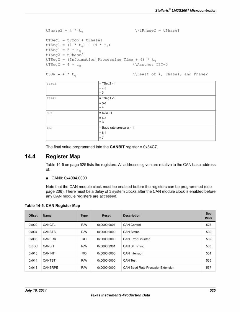
tPhase2 = 4 * tq \\tPhase2 = tPhase1
tTSeg1 = tProp + tPhase1 tTSeg1 = (1 * tq) + (4 * tq) tTSeg1 = 5 * tqtTSeg2 = tPhase2 tTSeg2 = (Information Processing Time + 4) * tqtTSeg2 = 4 * tq \\Assumes IPT=0
tSJW = 4 * tq \\Least of 4, Phase1, and Phase2
= TSeg2 -1= 4-1= 3
TSEG2
= TSeg1 -1= 5-1= 4
TSEG1
= SJW -1= 4-1= 3
SJW
= Baud rate prescaler - 1= 8-1= 7
BRP
The final value programmed into the CANBIT register = 0x34C7.
14.4 Register MapTable 14-5 on page 525 lists the registers. All addresses given are relative to the CAN base addressof:
CAN0: 0x4004.0000
Note that the CAN module clock must be enabled before the registers can be programmed (seepage 206). There must be a delay of 3 system clocks after the CAN module clock is enabled beforeany CAN module registers are accessed.
Table 14-5. CAN Register Map
SeepageDescriptionResetTypeNameOffset
528CAN Control0x0000.0001R/WCANCTL0x000
530CAN Status0x0000.0000R/WCANSTS0x004
532CAN Error Counter0x0000.0000ROCANERR0x008
533CAN Bit Timing0x0000.2301R/WCANBIT0x00C
534CAN Interrupt0x0000.0000ROCANINT0x010
535CAN Test0x0000.0000R/WCANTST0x014
537CAN Baud Rate Prescaler Extension0x0000.0000R/WCANBRPE0x018
525July 16, 2014Texas Instruments-Production Data
Stellaris® LM3S2601 Microcontroller
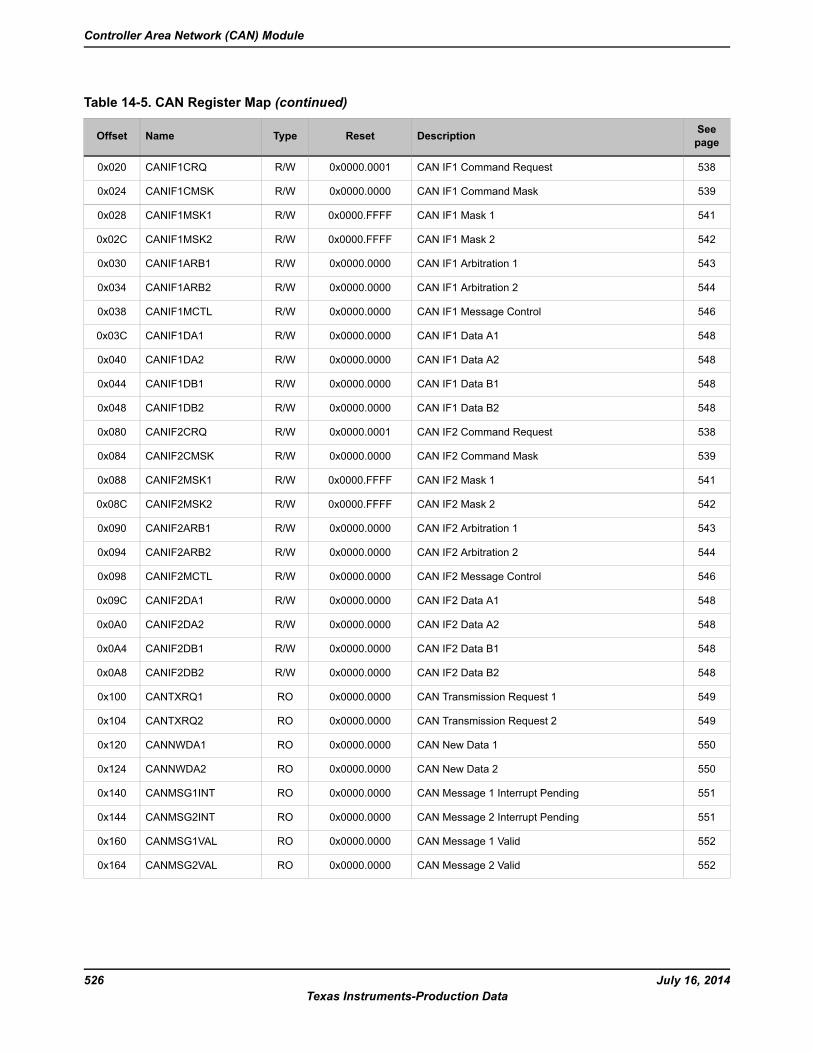
Table 14-5. CAN Register Map (continued)
SeepageDescriptionResetTypeNameOffset
538CAN IF1 Command Request0x0000.0001R/WCANIF1CRQ0x020
539CAN IF1 Command Mask0x0000.0000R/WCANIF1CMSK0x024
541CAN IF1 Mask 10x0000.FFFFR/WCANIF1MSK10x028
542CAN IF1 Mask 20x0000.FFFFR/WCANIF1MSK20x02C
543CAN IF1 Arbitration 10x0000.0000R/WCANIF1ARB10x030
544CAN IF1 Arbitration 20x0000.0000R/WCANIF1ARB20x034
546CAN IF1 Message Control0x0000.0000R/WCANIF1MCTL0x038
548CAN IF1 Data A10x0000.0000R/WCANIF1DA10x03C
548CAN IF1 Data A20x0000.0000R/WCANIF1DA20x040
548CAN IF1 Data B10x0000.0000R/WCANIF1DB10x044
548CAN IF1 Data B20x0000.0000R/WCANIF1DB20x048
538CAN IF2 Command Request0x0000.0001R/WCANIF2CRQ0x080
539CAN IF2 Command Mask0x0000.0000R/WCANIF2CMSK0x084
541CAN IF2 Mask 10x0000.FFFFR/WCANIF2MSK10x088
542CAN IF2 Mask 20x0000.FFFFR/WCANIF2MSK20x08C
543CAN IF2 Arbitration 10x0000.0000R/WCANIF2ARB10x090
544CAN IF2 Arbitration 20x0000.0000R/WCANIF2ARB20x094
546CAN IF2 Message Control0x0000.0000R/WCANIF2MCTL0x098
548CAN IF2 Data A10x0000.0000R/WCANIF2DA10x09C
548CAN IF2 Data A20x0000.0000R/WCANIF2DA20x0A0
548CAN IF2 Data B10x0000.0000R/WCANIF2DB10x0A4
548CAN IF2 Data B20x0000.0000R/WCANIF2DB20x0A8
549CAN Transmission Request 10x0000.0000ROCANTXRQ10x100
549CAN Transmission Request 20x0000.0000ROCANTXRQ20x104
550CAN New Data 10x0000.0000ROCANNWDA10x120
550CAN New Data 20x0000.0000ROCANNWDA20x124
551CAN Message 1 Interrupt Pending0x0000.0000ROCANMSG1INT0x140
551CAN Message 2 Interrupt Pending0x0000.0000ROCANMSG2INT0x144
552CAN Message 1 Valid0x0000.0000ROCANMSG1VAL0x160
552CAN Message 2 Valid0x0000.0000ROCANMSG2VAL0x164
July 16, 2014526Texas Instruments-Production Data
Controller Area Network (CAN) Module
14.5 CAN Register DescriptionsThe remainder of this section lists and describes the CAN registers, in numerical order by addressoffset. There are two sets of Interface Registers that are used to access the Message Objects inthe Message RAM: CANIF1x and CANIF2x. The function of the two sets are identical and are usedto queue transactions.
527July 16, 2014Texas Instruments-Production Data
Stellaris® LM3S2601 Microcontroller
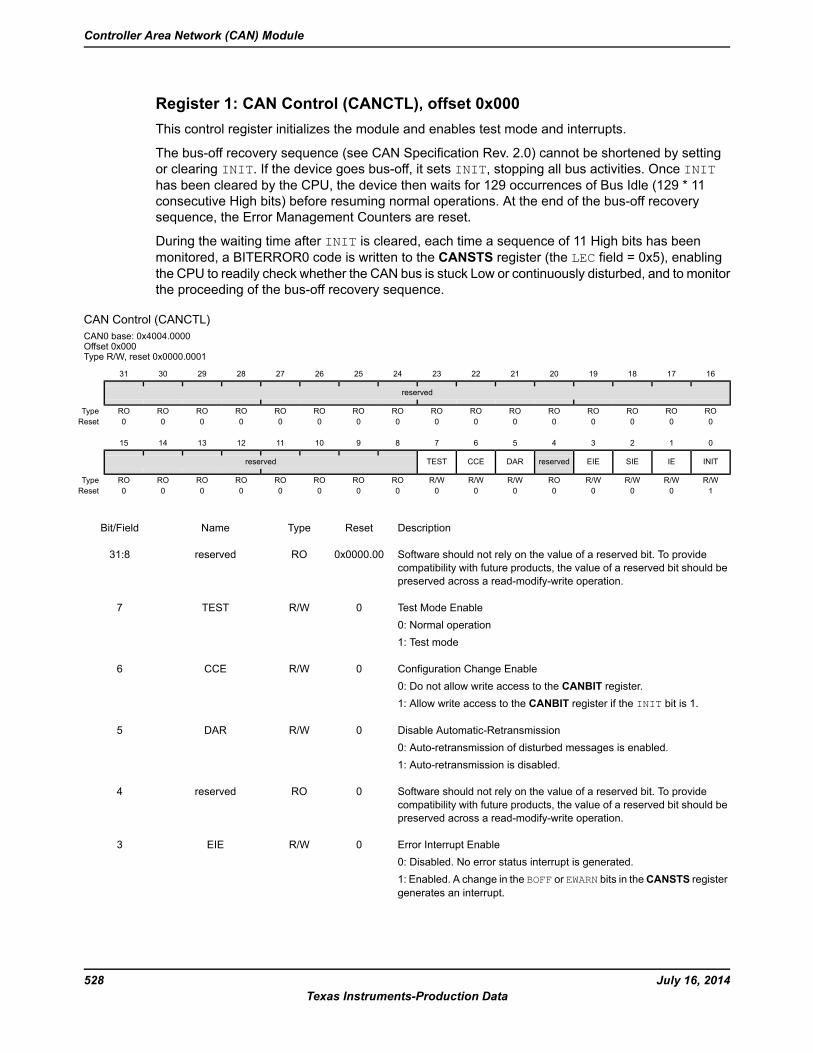
Register 1: CAN Control (CANCTL), offset 0x000This control register initializes the module and enables test mode and interrupts.
The bus-off recovery sequence (see CAN Specification Rev. 2.0) cannot be shortened by settingor clearing INIT. If the device goes bus-off, it sets INIT, stopping all bus activities. Once INIThas been cleared by the CPU, the device then waits for 129 occurrences of Bus Idle (129 * 11consecutive High bits) before resuming normal operations. At the end of the bus-off recoverysequence, the Error Management Counters are reset.
During the waiting time after INIT is cleared, each time a sequence of 11 High bits has beenmonitored, a BITERROR0 code is written to the CANSTS register (the LEC field = 0x5), enablingthe CPU to readily check whether the CAN bus is stuck Low or continuously disturbed, and to monitorthe proceeding of the bus-off recovery sequence.
CAN Control (CANCTL)CAN0 base: 0x4004.0000Offset 0x000Type R/W, reset 0x0000.0001
16171819202122232425262728293031
reserved
ROROROROROROROROROROROROROROROROType0000000000000000Reset
0123456789101112131415
INITIESIEEIEreservedDARCCETESTreserved
R/WR/WR/WR/WROR/WR/WR/WROROROROROROROROType1000000000000000Reset
DescriptionResetTypeNameBit/Field
Software should not rely on the value of a reserved bit. To providecompatibility with future products, the value of a reserved bit should bepreserved across a read-modify-write operation.
0x0000.00ROreserved31:8
Test Mode Enable0: Normal operation1: Test mode
0R/WTEST7
Configuration Change Enable0: Do not allow write access to the CANBIT register.1: Allow write access to the CANBIT register if the INIT bit is 1.
0R/WCCE6
Disable Automatic-Retransmission0: Auto-retransmission of disturbed messages is enabled.1: Auto-retransmission is disabled.
0R/WDAR5
Software should not rely on the value of a reserved bit. To providecompatibility with future products, the value of a reserved bit should bepreserved across a read-modify-write operation.
0ROreserved4
Error Interrupt Enable0: Disabled. No error status interrupt is generated.1: Enabled. A change in the BOFF or EWARN bits in theCANSTS registergenerates an interrupt.
0R/WEIE3
July 16, 2014528Texas Instruments-Production Data
Controller Area Network (CAN) Module
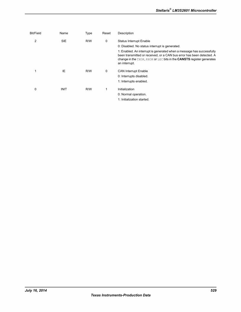
DescriptionResetTypeNameBit/Field
Status Interrupt Enable0: Disabled. No status interrupt is generated.1: Enabled. An interrupt is generated when a message has successfullybeen transmitted or received, or a CAN bus error has been detected. Achange in the TXOK, RXOK or LEC bits in theCANSTS register generatesan interrupt.
0R/WSIE2
CAN Interrupt Enable0: Interrupts disabled.1: Interrupts enabled.
0R/WIE1
Initialization0: Normal operation.1: Initialization started.
1R/WINIT0
529July 16, 2014Texas Instruments-Production Data
Stellaris® LM3S2601 Microcontroller
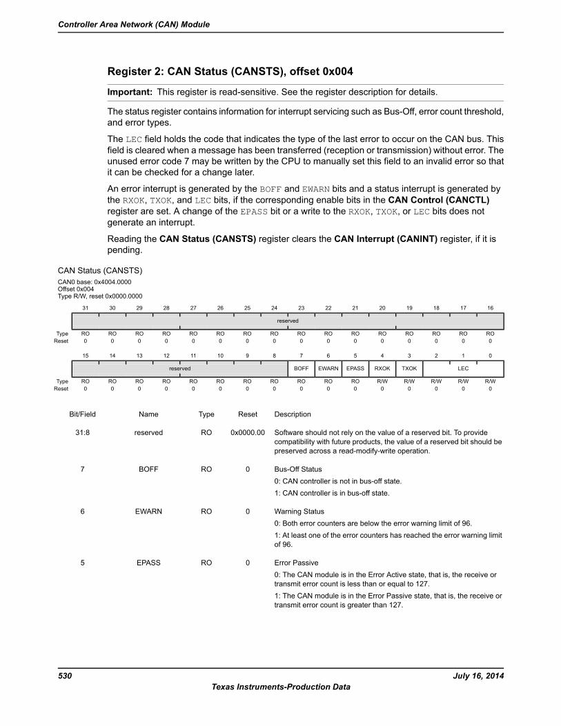
Register 2: CAN Status (CANSTS), offset 0x004
Important: This register is read-sensitive. See the register description for details.
The status register contains information for interrupt servicing such as Bus-Off, error count threshold,and error types.
The LEC field holds the code that indicates the type of the last error to occur on the CAN bus. Thisfield is cleared when a message has been transferred (reception or transmission) without error. Theunused error code 7 may be written by the CPU to manually set this field to an invalid error so thatit can be checked for a change later.
An error interrupt is generated by the BOFF and EWARN bits and a status interrupt is generated bythe RXOK, TXOK, and LEC bits, if the corresponding enable bits in the CAN Control (CANCTL)register are set. A change of the EPASS bit or a write to the RXOK, TXOK, or LEC bits does notgenerate an interrupt.
Reading the CAN Status (CANSTS) register clears the CAN Interrupt (CANINT) register, if it ispending.
CAN Status (CANSTS)CAN0 base: 0x4004.0000Offset 0x004Type R/W, reset 0x0000.0000
16171819202122232425262728293031
reserved
ROROROROROROROROROROROROROROROROType0000000000000000Reset
0123456789101112131415
LECTXOKRXOKEPASSEWARNBOFFreserved
R/WR/WR/WR/WR/WROROROROROROROROROROROType0000000000000000Reset
DescriptionResetTypeNameBit/Field
Software should not rely on the value of a reserved bit. To providecompatibility with future products, the value of a reserved bit should bepreserved across a read-modify-write operation.
0x0000.00ROreserved31:8
Bus-Off Status0: CAN controller is not in bus-off state.1: CAN controller is in bus-off state.
0ROBOFF7
Warning Status0: Both error counters are below the error warning limit of 96.1: At least one of the error counters has reached the error warning limitof 96.
0ROEWARN6
Error Passive0: The CAN module is in the Error Active state, that is, the receive ortransmit error count is less than or equal to 127.1: The CAN module is in the Error Passive state, that is, the receive ortransmit error count is greater than 127.
0ROEPASS5
July 16, 2014530Texas Instruments-Production Data
Controller Area Network (CAN) Module
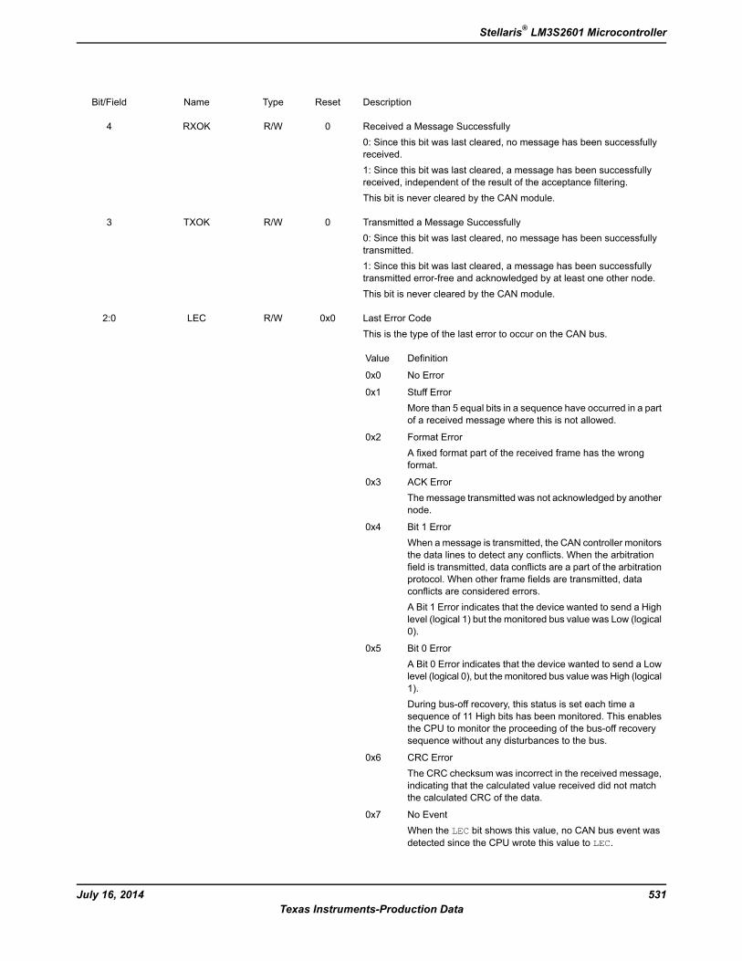
DescriptionResetTypeNameBit/Field
Received a Message Successfully0: Since this bit was last cleared, no message has been successfullyreceived.1: Since this bit was last cleared, a message has been successfullyreceived, independent of the result of the acceptance filtering.This bit is never cleared by the CAN module.
0R/WRXOK4
Transmitted a Message Successfully0: Since this bit was last cleared, no message has been successfullytransmitted.1: Since this bit was last cleared, a message has been successfullytransmitted error-free and acknowledged by at least one other node.This bit is never cleared by the CAN module.
0R/WTXOK3
Last Error CodeThis is the type of the last error to occur on the CAN bus.
DefinitionValue
No Error0x0
Stuff ErrorMore than 5 equal bits in a sequence have occurred in a partof a received message where this is not allowed.
0x1
Format ErrorA fixed format part of the received frame has the wrongformat.
0x2
ACK ErrorThemessage transmitted was not acknowledged by anothernode.
0x3
Bit 1 ErrorWhen a message is transmitted, the CAN controller monitorsthe data lines to detect any conflicts. When the arbitrationfield is transmitted, data conflicts are a part of the arbitrationprotocol. When other frame fields are transmitted, dataconflicts are considered errors.A Bit 1 Error indicates that the device wanted to send a Highlevel (logical 1) but the monitored bus value was Low (logical0).
0x4
Bit 0 ErrorA Bit 0 Error indicates that the device wanted to send a Lowlevel (logical 0), but the monitored bus value was High (logical1).During bus-off recovery, this status is set each time asequence of 11 High bits has been monitored. This enablesthe CPU to monitor the proceeding of the bus-off recoverysequence without any disturbances to the bus.
0x5
CRC ErrorThe CRC checksum was incorrect in the received message,indicating that the calculated value received did not matchthe calculated CRC of the data.
0x6
No EventWhen the LEC bit shows this value, no CAN bus event wasdetected since the CPU wrote this value to LEC.
0x7
0x0R/WLEC2:0
531July 16, 2014Texas Instruments-Production Data
Stellaris® LM3S2601 Microcontroller
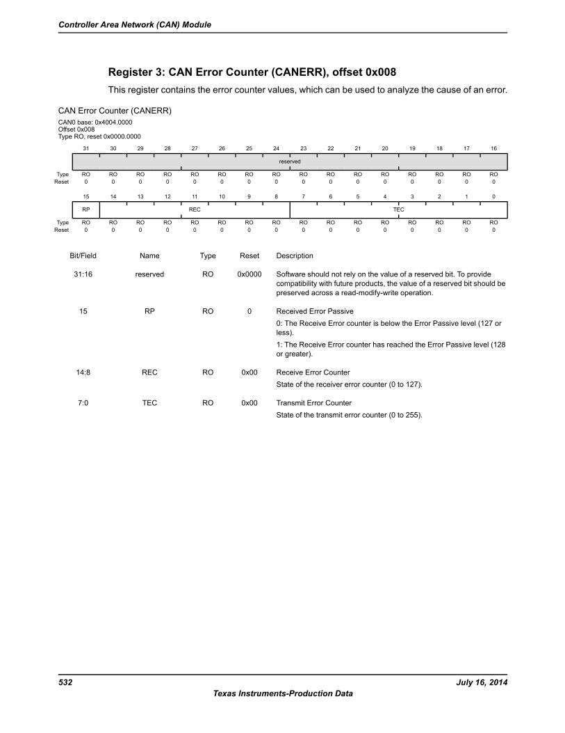
Register 3: CAN Error Counter (CANERR), offset 0x008This register contains the error counter values, which can be used to analyze the cause of an error.
CAN Error Counter (CANERR)CAN0 base: 0x4004.0000Offset 0x008Type RO, reset 0x0000.0000
16171819202122232425262728293031
reserved
ROROROROROROROROROROROROROROROROType0000000000000000Reset
0123456789101112131415
TECRECRP
ROROROROROROROROROROROROROROROROType0000000000000000Reset
DescriptionResetTypeNameBit/Field
Software should not rely on the value of a reserved bit. To providecompatibility with future products, the value of a reserved bit should bepreserved across a read-modify-write operation.
0x0000ROreserved31:16
Received Error Passive0: The Receive Error counter is below the Error Passive level (127 orless).1: The Receive Error counter has reached the Error Passive level (128or greater).
0RORP15
Receive Error CounterState of the receiver error counter (0 to 127).
0x00ROREC14:8
Transmit Error CounterState of the transmit error counter (0 to 255).
0x00ROTEC7:0
July 16, 2014532Texas Instruments-Production Data
Controller Area Network (CAN) Module
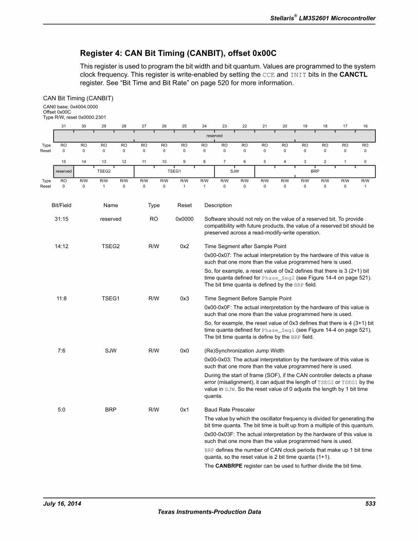
Register 4: CAN Bit Timing (CANBIT), offset 0x00CThis register is used to program the bit width and bit quantum. Values are programmed to the systemclock frequency. This register is write-enabled by setting the CCE and INIT bits in the CANCTLregister. See “Bit Time and Bit Rate” on page 520 for more information.
CAN Bit Timing (CANBIT)CAN0 base: 0x4004.0000Offset 0x00CType R/W, reset 0x0000.2301
16171819202122232425262728293031
reserved
ROROROROROROROROROROROROROROROROType0000000000000000Reset
0123456789101112131415
BRPSJWTSEG1TSEG2reserved
R/WR/WR/WR/WR/WR/WR/WR/WR/WR/WR/WR/WR/WR/WR/WROType1000000011000100Reset
DescriptionResetTypeNameBit/Field
Software should not rely on the value of a reserved bit. To providecompatibility with future products, the value of a reserved bit should bepreserved across a read-modify-write operation.
0x0000ROreserved31:15
Time Segment after Sample Point0x00-0x07: The actual interpretation by the hardware of this value issuch that one more than the value programmed here is used.So, for example, a reset value of 0x2 defines that there is 3 (2+1) bittime quanta defined for Phase_Seg2 (see Figure 14-4 on page 521).The bit time quanta is defined by the BRP field.
0x2R/WTSEG214:12
Time Segment Before Sample Point0x00-0x0F: The actual interpretation by the hardware of this value issuch that one more than the value programmed here is used.So, for example, the reset value of 0x3 defines that there is 4 (3+1) bittime quanta defined for Phase_Seg1 (see Figure 14-4 on page 521).The bit time quanta is define by the BRP field.
0x3R/WTSEG111:8
(Re)Synchronization Jump Width0x00-0x03: The actual interpretation by the hardware of this value issuch that one more than the value programmed here is used.During the start of frame (SOF), if the CAN controller detects a phaseerror (misalignment), it can adjust the length of TSEG2 or TSEG1 by thevalue in SJW. So the reset value of 0 adjusts the length by 1 bit timequanta.
0x0R/WSJW7:6
Baud Rate PrescalerThe value by which the oscillator frequency is divided for generating thebit time quanta. The bit time is built up from a multiple of this quantum.0x00-0x03F: The actual interpretation by the hardware of this value issuch that one more than the value programmed here is used.BRP defines the number of CAN clock periods that make up 1 bit timequanta, so the reset value is 2 bit time quanta (1+1).The CANBRPE register can be used to further divide the bit time.
0x1R/WBRP5:0
533July 16, 2014Texas Instruments-Production Data
Stellaris® LM3S2601 Microcontroller
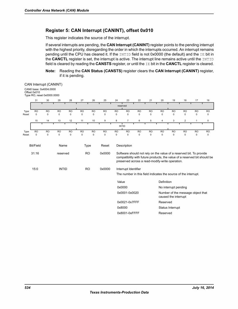
Register 5: CAN Interrupt (CANINT), offset 0x010This register indicates the source of the interrupt.
If several interrupts are pending, theCAN Interrupt (CANINT) register points to the pending interruptwith the highest priority, disregarding the order in which the interrupts occurred. An interrupt remainspending until the CPU has cleared it. If the INTID field is not 0x0000 (the default) and the IE bit inthe CANCTL register is set, the interrupt is active. The interrupt line remains active until the INTIDfield is cleared by reading theCANSTS register, or until the IE bit in theCANCTL register is cleared.
Note: Reading the CAN Status (CANSTS) register clears the CAN Interrupt (CANINT) register,if it is pending.
CAN Interrupt (CANINT)CAN0 base: 0x4004.0000Offset 0x010Type RO, reset 0x0000.0000
16171819202122232425262728293031
reserved
ROROROROROROROROROROROROROROROROType0000000000000000Reset
0123456789101112131415
INTID
ROROROROROROROROROROROROROROROROType0000000000000000Reset
DescriptionResetTypeNameBit/Field
Software should not rely on the value of a reserved bit. To providecompatibility with future products, the value of a reserved bit should bepreserved across a read-modify-write operation.
0x0000ROreserved31:16
Interrupt IdentifierThe number in this field indicates the source of the interrupt.
DefinitionValue
No interrupt pending0x0000
Number of the message object thatcaused the interrupt
0x0001-0x0020
Reserved0x0021-0x7FFF
Status Interrupt0x8000
Reserved0x8001-0xFFFF
0x0000ROINTID15:0
July 16, 2014534Texas Instruments-Production Data
Controller Area Network (CAN) Module
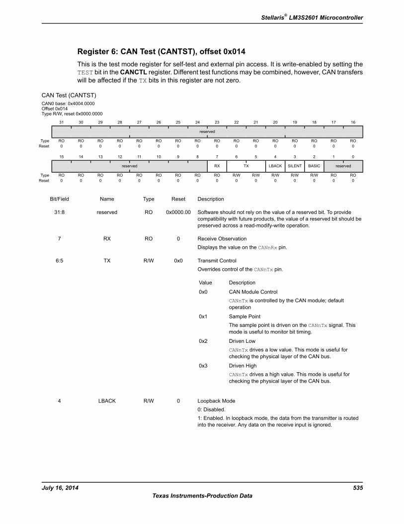
Register 6: CAN Test (CANTST), offset 0x014This is the test mode register for self-test and external pin access. It is write-enabled by setting theTEST bit in theCANCTL register. Different test functions may be combined, however, CAN transferswill be affected if the TX bits in this register are not zero.
CAN Test (CANTST)CAN0 base: 0x4004.0000Offset 0x014Type R/W, reset 0x0000.0000
16171819202122232425262728293031
reserved
ROROROROROROROROROROROROROROROROType0000000000000000Reset
0123456789101112131415
reservedBASICSILENTLBACKTXRXreserved
ROROR/WR/WR/WR/WR/WROROROROROROROROROType0000000000000000Reset
DescriptionResetTypeNameBit/Field
Software should not rely on the value of a reserved bit. To providecompatibility with future products, the value of a reserved bit should bepreserved across a read-modify-write operation.
0x0000.00ROreserved31:8
Receive ObservationDisplays the value on the CANnRx pin.
0RORX7
Transmit ControlOverrides control of the CANnTx pin.
DescriptionValue
CAN Module ControlCANnTx is controlled by the CAN module; defaultoperation
0x0
Sample PointThe sample point is driven on the CANnTx signal. Thismode is useful to monitor bit timing.
0x1
Driven LowCANnTx drives a low value. This mode is useful forchecking the physical layer of the CAN bus.
0x2
Driven HighCANnTx drives a high value. This mode is useful forchecking the physical layer of the CAN bus.
0x3
0x0R/WTX6:5
Loopback Mode0: Disabled.1: Enabled. In loopback mode, the data from the transmitter is routedinto the receiver. Any data on the receive input is ignored.
0R/WLBACK4
535July 16, 2014Texas Instruments-Production Data
Stellaris® LM3S2601 Microcontroller
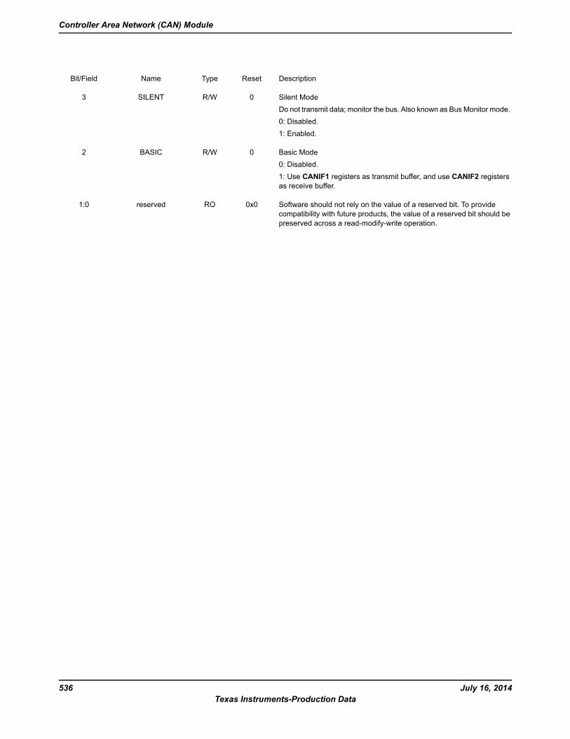
DescriptionResetTypeNameBit/Field
Silent ModeDo not transmit data; monitor the bus. Also known as Bus Monitor mode.0: Disabled.1: Enabled.
0R/WSILENT3
Basic Mode0: Disabled.1: Use CANIF1 registers as transmit buffer, and use CANIF2 registersas receive buffer.
0R/WBASIC2
Software should not rely on the value of a reserved bit. To providecompatibility with future products, the value of a reserved bit should bepreserved across a read-modify-write operation.
0x0ROreserved1:0
July 16, 2014536Texas Instruments-Production Data
Controller Area Network (CAN) Module
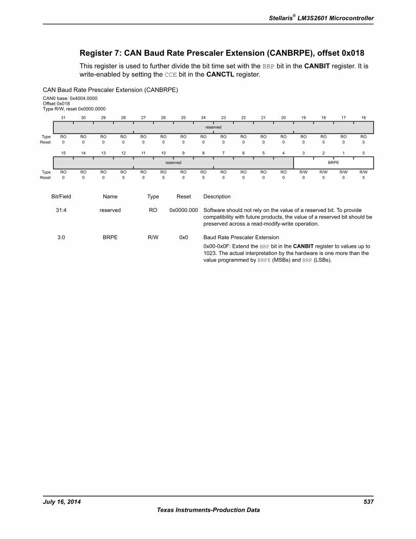
Register 7: CAN Baud Rate Prescaler Extension (CANBRPE), offset 0x018This register is used to further divide the bit time set with the BRP bit in the CANBIT register. It iswrite-enabled by setting the CCE bit in the CANCTL register.
CAN Baud Rate Prescaler Extension (CANBRPE)CAN0 base: 0x4004.0000Offset 0x018Type R/W, reset 0x0000.0000
16171819202122232425262728293031
reserved
ROROROROROROROROROROROROROROROROType0000000000000000Reset
0123456789101112131415
BRPEreserved
R/WR/WR/WR/WROROROROROROROROROROROROType0000000000000000Reset
DescriptionResetTypeNameBit/Field
Software should not rely on the value of a reserved bit. To providecompatibility with future products, the value of a reserved bit should bepreserved across a read-modify-write operation.
0x0000.000ROreserved31:4
Baud Rate Prescaler Extension0x00-0x0F: Extend the BRP bit in the CANBIT register to values up to1023. The actual interpretation by the hardware is one more than thevalue programmed by BRPE (MSBs) and BRP (LSBs).
0x0R/WBRPE3:0
537July 16, 2014Texas Instruments-Production Data
Stellaris® LM3S2601 Microcontroller
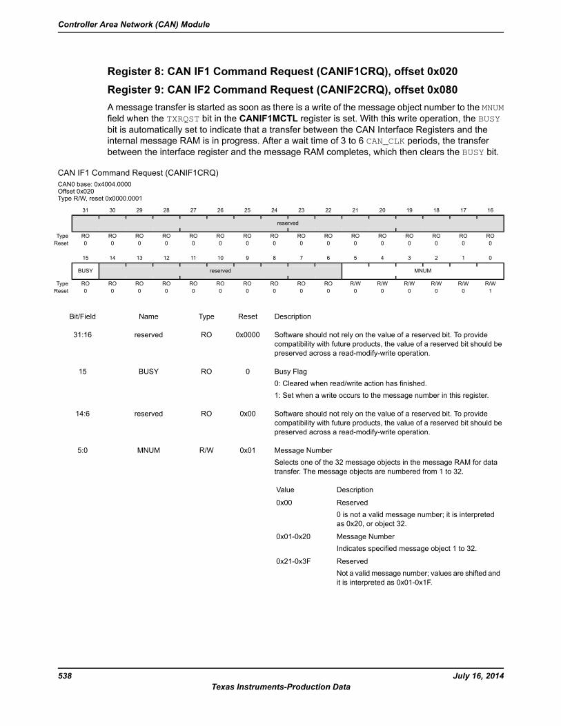
Register 8: CAN IF1 Command Request (CANIF1CRQ), offset 0x020Register 9: CAN IF2 Command Request (CANIF2CRQ), offset 0x080A message transfer is started as soon as there is a write of the message object number to the MNUMfield when the TXRQST bit in the CANIF1MCTL register is set. With this write operation, the BUSYbit is automatically set to indicate that a transfer between the CAN Interface Registers and theinternal message RAM is in progress. After a wait time of 3 to 6 CAN_CLK periods, the transferbetween the interface register and the message RAM completes, which then clears the BUSY bit.
CAN IF1 Command Request (CANIF1CRQ)CAN0 base: 0x4004.0000Offset 0x020Type R/W, reset 0x0000.0001
16171819202122232425262728293031
reserved
ROROROROROROROROROROROROROROROROType0000000000000000Reset
0123456789101112131415
MNUMreservedBUSY
R/WR/WR/WR/WR/WR/WROROROROROROROROROROType1000000000000000Reset
DescriptionResetTypeNameBit/Field
Software should not rely on the value of a reserved bit. To providecompatibility with future products, the value of a reserved bit should bepreserved across a read-modify-write operation.
0x0000ROreserved31:16
Busy Flag0: Cleared when read/write action has finished.1: Set when a write occurs to the message number in this register.
0ROBUSY15
Software should not rely on the value of a reserved bit. To providecompatibility with future products, the value of a reserved bit should bepreserved across a read-modify-write operation.
0x00ROreserved14:6
Message NumberSelects one of the 32 message objects in the message RAM for datatransfer. The message objects are numbered from 1 to 32.
DescriptionValue
Reserved0 is not a valid message number; it is interpretedas 0x20, or object 32.
0x00
Message NumberIndicates specified message object 1 to 32.
0x01-0x20
ReservedNot a valid message number; values are shifted andit is interpreted as 0x01-0x1F.
0x21-0x3F
0x01R/WMNUM5:0
July 16, 2014538Texas Instruments-Production Data
Controller Area Network (CAN) Module
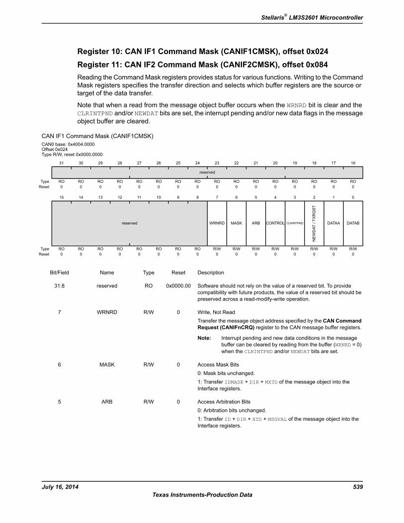
Register 10: CAN IF1 Command Mask (CANIF1CMSK), offset 0x024Register 11: CAN IF2 Command Mask (CANIF2CMSK), offset 0x084Reading the CommandMask registers provides status for various functions. Writing to the CommandMask registers specifies the transfer direction and selects which buffer registers are the source ortarget of the data transfer.
Note that when a read from the message object buffer occurs when the WRNRD bit is clear and theCLRINTPND and/or NEWDAT bits are set, the interrupt pending and/or new data flags in the messageobject buffer are cleared.
CAN IF1 Command Mask (CANIF1CMSK)CAN0 base: 0x4004.0000Offset 0x024Type R/W, reset 0x0000.0000
16171819202122232425262728293031
reserved
ROROROROROROROROROROROROROROROROType0000000000000000Reset
0123456789101112131415
DATABDATAA
NEWDAT
/TXRQST
CLRINTPNDCONTROLARBMASKWRNRDreserved
R/WR/WR/WR/WR/WR/WR/WR/WROROROROROROROROType0000000000000000Reset
DescriptionResetTypeNameBit/Field
Software should not rely on the value of a reserved bit. To providecompatibility with future products, the value of a reserved bit should bepreserved across a read-modify-write operation.
0x0000.00ROreserved31:8
Write, Not ReadTransfer the message object address specified by the CAN CommandRequest (CANIFnCRQ) register to the CAN message buffer registers.
Note: Interrupt pending and new data conditions in the messagebuffer can be cleared by reading from the buffer (WRNRD = 0)when the CLRINTPND and/or NEWDAT bits are set.
0R/WWRNRD7
Access Mask Bits0: Mask bits unchanged.1: Transfer IDMASK + DIR + MXTD of the message object into theInterface registers.
0R/WMASK6
Access Arbitration Bits0: Arbitration bits unchanged.1: Transfer ID + DIR + XTD + MSGVAL of the message object into theInterface registers.
0R/WARB5
539July 16, 2014Texas Instruments-Production Data
Stellaris® LM3S2601 Microcontroller
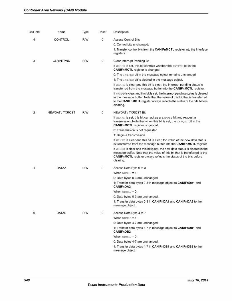
DescriptionResetTypeNameBit/Field
Access Control Bits0: Control bits unchanged.1: Transfer control bits from theCANIFnMCTL register into the Interfaceregisters.
0R/WCONTROL4
Clear Interrupt Pending BitIf WRNRD is set, this bit controls whether the INTPND bit in theCANIFnMCTL register is changed.0: The INTPND bit in the message object remains unchanged.1: The INTPND bit is cleared in the message object.If WRNRD is clear and this bit is clear, the interrupt pending status istransferred from the message buffer into the CANIFnMCTL register.If WRNRD is clear and this bit is set, the interrupt pending status is clearedin the message buffer. Note that the value of this bit that is transferredto theCANIFnMCTL register always reflects the status of the bits beforeclearing.
0R/WCLRINTPND3
NEWDAT / TXRQST BitIf WRNRD is set, this bit can act as a TXRQST bit and request atransmission. Note that when this bit is set, the TXRQST bit in theCANIFnMCTL register is ignored.0: Transmission is not requested1: Begin a transmissionIf WRNRD is clear and this bit is clear, the value of the new data statusis transferred from the message buffer into the CANIFnMCTL register.If WRNRD is clear and this bit is set, the new data status is cleared in themessage buffer. Note that the value of this bit that is transferred to theCANIFnMCTL register always reflects the status of the bits beforeclearing.
0R/WNEWDAT / TXRQST2
Access Data Byte 0 to 3When WRNRD = 1:0: Data bytes 0-3 are unchanged.1: Transfer data bytes 0-3 in message object to CANIFnDA1 andCANIFnDA2.When WRNRD = 0:0: Data bytes 0-3 are unchanged.1: Transfer data bytes 0-3 in CANIFnDA1 and CANIFnDA2 to themessage object.
0R/WDATAA1
Access Data Byte 4 to 7When WRNRD = 1:0: Data bytes 4-7 are unchanged.1: Transfer data bytes 4-7 in message object to CANIFnDB1 andCANIFnDB2.When WRNRD = 0:0: Data bytes 4-7 are unchanged.1: Transfer data bytes 4-7 in CANIFnDB1 and CANIFnDB2 to themessage object.
0R/WDATAB0
July 16, 2014540Texas Instruments-Production Data
Controller Area Network (CAN) Module
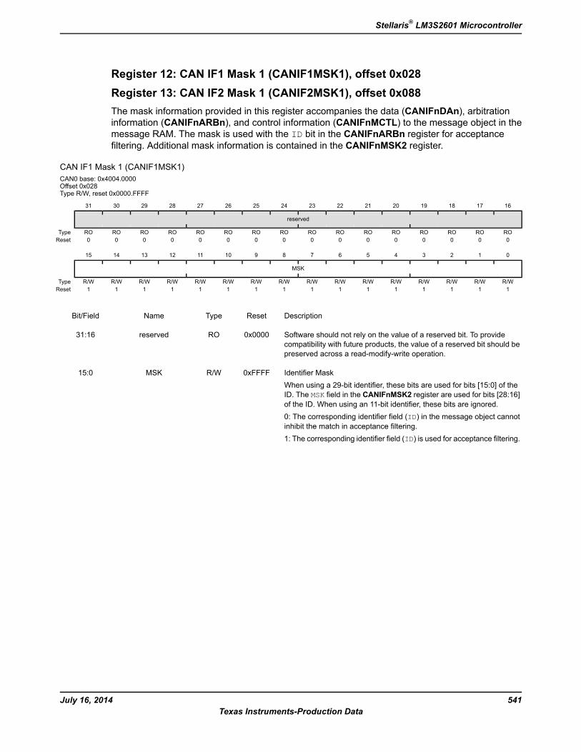
Register 12: CAN IF1 Mask 1 (CANIF1MSK1), offset 0x028Register 13: CAN IF2 Mask 1 (CANIF2MSK1), offset 0x088The mask information provided in this register accompanies the data (CANIFnDAn), arbitrationinformation (CANIFnARBn), and control information (CANIFnMCTL) to the message object in themessage RAM. The mask is used with the ID bit in the CANIFnARBn register for acceptancefiltering. Additional mask information is contained in the CANIFnMSK2 register.
CAN IF1 Mask 1 (CANIF1MSK1)CAN0 base: 0x4004.0000Offset 0x028Type R/W, reset 0x0000.FFFF
16171819202122232425262728293031
reserved
ROROROROROROROROROROROROROROROROType0000000000000000Reset
0123456789101112131415
MSK
R/WR/WR/WR/WR/WR/WR/WR/WR/WR/WR/WR/WR/WR/WR/WR/WType1111111111111111Reset
DescriptionResetTypeNameBit/Field
Software should not rely on the value of a reserved bit. To providecompatibility with future products, the value of a reserved bit should bepreserved across a read-modify-write operation.
0x0000ROreserved31:16
Identifier MaskWhen using a 29-bit identifier, these bits are used for bits [15:0] of theID. The MSK field in the CANIFnMSK2 register are used for bits [28:16]of the ID. When using an 11-bit identifier, these bits are ignored.0: The corresponding identifier field (ID) in the message object cannotinhibit the match in acceptance filtering.1: The corresponding identifier field (ID) is used for acceptance filtering.
0xFFFFR/WMSK15:0
541July 16, 2014Texas Instruments-Production Data
Stellaris® LM3S2601 Microcontroller
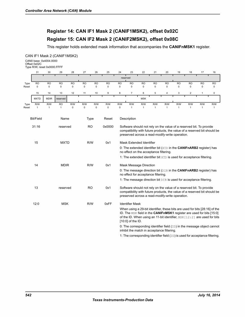
Register 14: CAN IF1 Mask 2 (CANIF1MSK2), offset 0x02CRegister 15: CAN IF2 Mask 2 (CANIF2MSK2), offset 0x08CThis register holds extended mask information that accompanies the CANIFnMSK1 register.
CAN IF1 Mask 2 (CANIF1MSK2)CAN0 base: 0x4004.0000Offset 0x02CType R/W, reset 0x0000.FFFF
16171819202122232425262728293031
reserved
ROROROROROROROROROROROROROROROROType0000000000000000Reset
0123456789101112131415
MSKreservedMDIRMXTD
R/WR/WR/WR/WR/WR/WR/WR/WR/WR/WR/WR/WR/WROR/WR/WType1111111100000111Reset
DescriptionResetTypeNameBit/Field
Software should not rely on the value of a reserved bit. To providecompatibility with future products, the value of a reserved bit should bepreserved across a read-modify-write operation.
0x0000ROreserved31:16
Mask Extended Identifier0: The extended identifier bit (XTD in the CANIFnARB2 register) hasno effect on the acceptance filtering.1: The extended identifier bit XTD is used for acceptance filtering.
0x1R/WMXTD15
Mask Message Direction0: The message direction bit (DIR in the CANIFnARB2 register) hasno effect for acceptance filtering.1: The message direction bit DIR is used for acceptance filtering.
0x1R/WMDIR14
Software should not rely on the value of a reserved bit. To providecompatibility with future products, the value of a reserved bit should bepreserved across a read-modify-write operation.
0x1ROreserved13
Identifier MaskWhen using a 29-bit identifier, these bits are used for bits [28:16] of theID. The MSK field in the CANIFnMSK1 register are used for bits [15:0]of the ID. When using an 11-bit identifier, MSK[12:2] are used for bits[10:0] of the ID.0: The corresponding identifier field (ID) in the message object cannotinhibit the match in acceptance filtering.1: The corresponding identifier field (ID) is used for acceptance filtering.
0xFFR/WMSK12:0
July 16, 2014542Texas Instruments-Production Data
Controller Area Network (CAN) Module
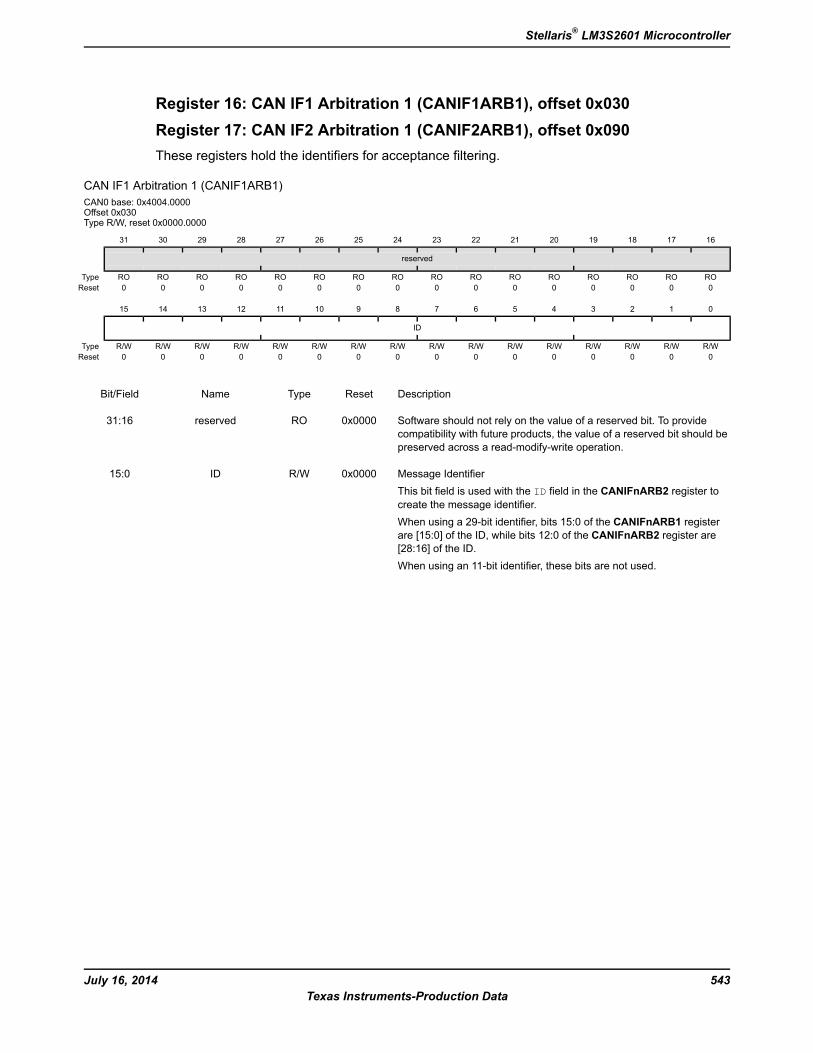
Register 16: CAN IF1 Arbitration 1 (CANIF1ARB1), offset 0x030Register 17: CAN IF2 Arbitration 1 (CANIF2ARB1), offset 0x090These registers hold the identifiers for acceptance filtering.
CAN IF1 Arbitration 1 (CANIF1ARB1)CAN0 base: 0x4004.0000Offset 0x030Type R/W, reset 0x0000.0000
16171819202122232425262728293031
reserved
ROROROROROROROROROROROROROROROROType0000000000000000Reset
0123456789101112131415
ID
R/WR/WR/WR/WR/WR/WR/WR/WR/WR/WR/WR/WR/WR/WR/WR/WType0000000000000000Reset
DescriptionResetTypeNameBit/Field
Software should not rely on the value of a reserved bit. To providecompatibility with future products, the value of a reserved bit should bepreserved across a read-modify-write operation.
0x0000ROreserved31:16
Message IdentifierThis bit field is used with the ID field in the CANIFnARB2 register tocreate the message identifier.When using a 29-bit identifier, bits 15:0 of the CANIFnARB1 registerare [15:0] of the ID, while bits 12:0 of the CANIFnARB2 register are[28:16] of the ID.When using an 11-bit identifier, these bits are not used.
0x0000R/WID15:0
543July 16, 2014Texas Instruments-Production Data
Stellaris® LM3S2601 Microcontroller
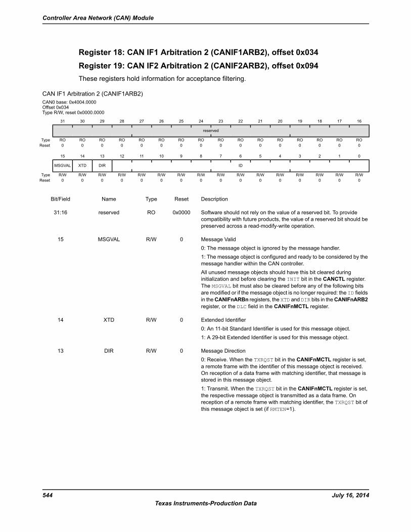
Register 18: CAN IF1 Arbitration 2 (CANIF1ARB2), offset 0x034Register 19: CAN IF2 Arbitration 2 (CANIF2ARB2), offset 0x094These registers hold information for acceptance filtering.
CAN IF1 Arbitration 2 (CANIF1ARB2)CAN0 base: 0x4004.0000Offset 0x034Type R/W, reset 0x0000.0000
16171819202122232425262728293031
reserved
ROROROROROROROROROROROROROROROROType0000000000000000Reset
0123456789101112131415
IDDIRXTDMSGVAL
R/WR/WR/WR/WR/WR/WR/WR/WR/WR/WR/WR/WR/WR/WR/WR/WType0000000000000000Reset
DescriptionResetTypeNameBit/Field
Software should not rely on the value of a reserved bit. To providecompatibility with future products, the value of a reserved bit should bepreserved across a read-modify-write operation.
0x0000ROreserved31:16
Message Valid0: The message object is ignored by the message handler.1: The message object is configured and ready to be considered by themessage handler within the CAN controller.All unused message objects should have this bit cleared duringinitialization and before clearing the INIT bit in the CANCTL register.The MSGVAL bit must also be cleared before any of the following bitsare modified or if the message object is no longer required: the ID fieldsin theCANIFnARBn registers, the XTD and DIR bits in theCANIFnARB2register, or the DLC field in the CANIFnMCTL register.
0R/WMSGVAL15
Extended Identifier0: An 11-bit Standard Identifier is used for this message object.1: A 29-bit Extended Identifier is used for this message object.
0R/WXTD14
Message Direction0: Receive. When the TXRQST bit in the CANIFnMCTL register is set,a remote frame with the identifier of this message object is received.On reception of a data frame with matching identifier, that message isstored in this message object.1: Transmit. When the TXRQST bit in the CANIFnMCTL register is set,the respective message object is transmitted as a data frame. Onreception of a remote frame with matching identifier, the TXRQST bit ofthis message object is set (if RMTEN=1).
0R/WDIR13
July 16, 2014544Texas Instruments-Production Data
Controller Area Network (CAN) Module

DescriptionResetTypeNameBit/Field
Message IdentifierThis bit field is used with the ID field in the CANIFnARB2 register tocreate the message identifier.When using a 29-bit identifier, ID[15:0] of the CANIFnARB1 registerare [15:0] of the ID, while these bits, ID[12:0], are [28:16] of the ID.When using an 11-bit identifier, ID[12:2] are used for bits [10:0] ofthe ID. The ID field in the CANIFnARB1 register is ignored.
0x000R/WID12:0
545July 16, 2014Texas Instruments-Production Data
Stellaris® LM3S2601 Microcontroller
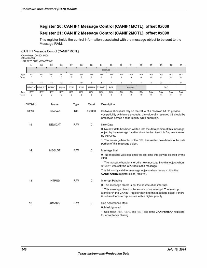
Register 20: CAN IF1 Message Control (CANIF1MCTL), offset 0x038Register 21: CAN IF2 Message Control (CANIF2MCTL), offset 0x098This register holds the control information associated with the message object to be sent to theMessage RAM.
CAN IF1 Message Control (CANIF1MCTL)CAN0 base: 0x4004.0000Offset 0x038Type R/W, reset 0x0000.0000
16171819202122232425262728293031
reserved
ROROROROROROROROROROROROROROROROType0000000000000000Reset
0123456789101112131415
DLCreservedEOBTXRQSTRMTENRXIETXIEUMASKINTPNDMSGLSTNEWDAT
R/WR/WR/WR/WROROROR/WR/WR/WR/WR/WR/WR/WR/WR/WType0000000000000000Reset
DescriptionResetTypeNameBit/Field
Software should not rely on the value of a reserved bit. To providecompatibility with future products, the value of a reserved bit should bepreserved across a read-modify-write operation.
0x0000ROreserved31:16
New Data0: No new data has been written into the data portion of this messageobject by the message handler since the last time this flag was clearedby the CPU.1: The message handler or the CPU has written new data into the dataportion of this message object.
0R/WNEWDAT15
Message Lost0 : No message was lost since the last time this bit was cleared by theCPU.1: The message handler stored a new message into this object whenNEWDAT was set; the CPU has lost a message.This bit is only valid for message objects when the DIR bit in theCANIFnARB2 register clear (receive).
0R/WMSGLST14
Interrupt Pending0: This message object is not the source of an interrupt.1: This message object is the source of an interrupt. The interruptidentifier in the CANINT register points to this message object if thereis not another interrupt source with a higher priority.
0R/WINTPND13
Use Acceptance Mask0: Mask ignored.1: Use mask (MSK, MXTD, and MDIR bits in the CANIFnMSKn registers)for acceptance filtering.
0R/WUMASK12
July 16, 2014546Texas Instruments-Production Data
Controller Area Network (CAN) Module
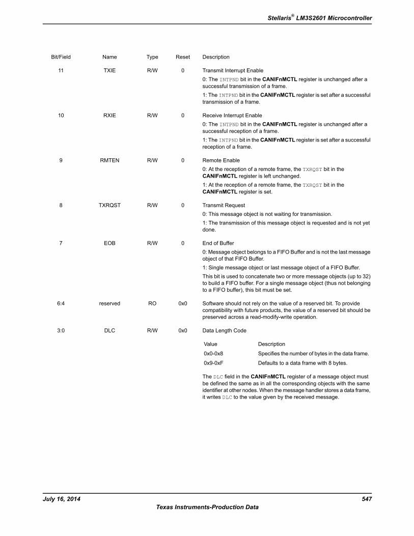
DescriptionResetTypeNameBit/Field
Transmit Interrupt Enable0: The INTPND bit in the CANIFnMCTL register is unchanged after asuccessful transmission of a frame.1: The INTPND bit in theCANIFnMCTL register is set after a successfultransmission of a frame.
0R/WTXIE11
Receive Interrupt Enable0: The INTPND bit in the CANIFnMCTL register is unchanged after asuccessful reception of a frame.1: The INTPND bit in theCANIFnMCTL register is set after a successfulreception of a frame.
0R/WRXIE10
Remote Enable0: At the reception of a remote frame, the TXRQST bit in theCANIFnMCTL register is left unchanged.1: At the reception of a remote frame, the TXRQST bit in theCANIFnMCTL register is set.
0R/WRMTEN9
Transmit Request0: This message object is not waiting for transmission.1: The transmission of this message object is requested and is not yetdone.
0R/WTXRQST8
End of Buffer0: Message object belongs to a FIFO Buffer and is not the last messageobject of that FIFO Buffer.1: Single message object or last message object of a FIFO Buffer.This bit is used to concatenate two or more message objects (up to 32)to build a FIFO buffer. For a single message object (thus not belongingto a FIFO buffer), this bit must be set.
0R/WEOB7
Software should not rely on the value of a reserved bit. To providecompatibility with future products, the value of a reserved bit should bepreserved across a read-modify-write operation.
0x0ROreserved6:4
Data Length Code
DescriptionValue
Specifies the number of bytes in the data frame.0x0-0x8
Defaults to a data frame with 8 bytes.0x9-0xF
The DLC field in the CANIFnMCTL register of a message object mustbe defined the same as in all the corresponding objects with the sameidentifier at other nodes.When themessage handler stores a data frame,it writes DLC to the value given by the received message.
0x0R/WDLC3:0
547July 16, 2014Texas Instruments-Production Data
Stellaris® LM3S2601 Microcontroller
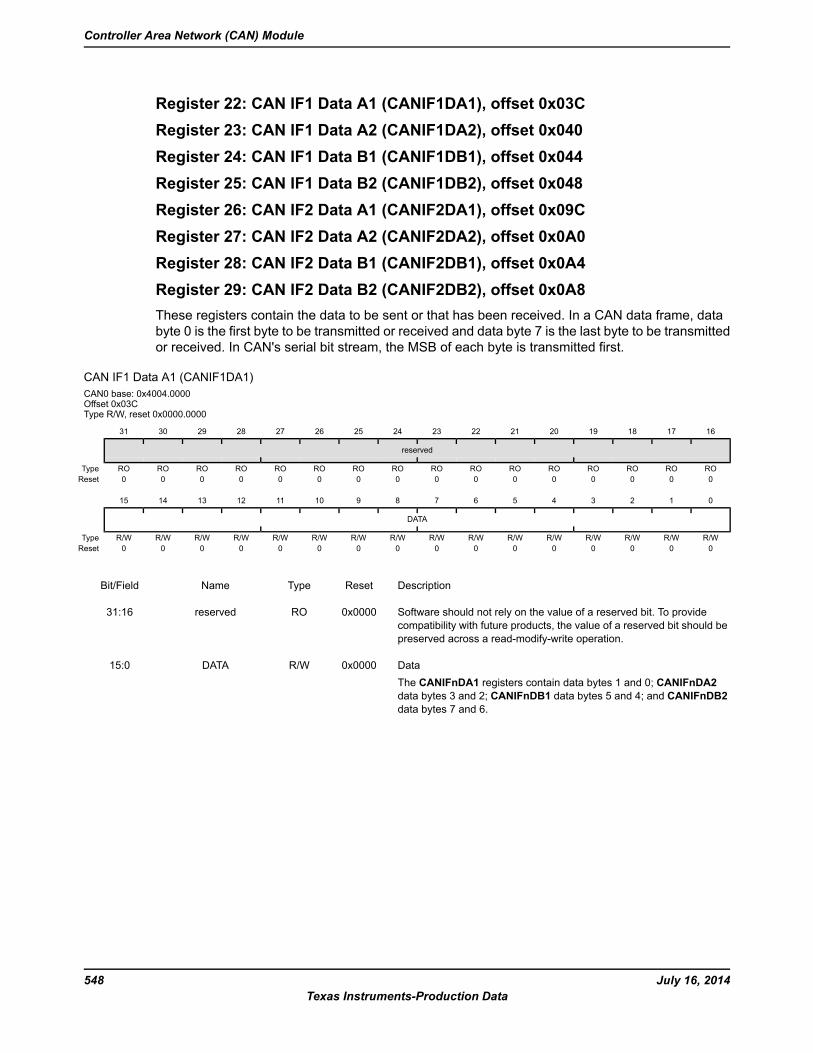
Register 22: CAN IF1 Data A1 (CANIF1DA1), offset 0x03CRegister 23: CAN IF1 Data A2 (CANIF1DA2), offset 0x040Register 24: CAN IF1 Data B1 (CANIF1DB1), offset 0x044Register 25: CAN IF1 Data B2 (CANIF1DB2), offset 0x048Register 26: CAN IF2 Data A1 (CANIF2DA1), offset 0x09CRegister 27: CAN IF2 Data A2 (CANIF2DA2), offset 0x0A0Register 28: CAN IF2 Data B1 (CANIF2DB1), offset 0x0A4Register 29: CAN IF2 Data B2 (CANIF2DB2), offset 0x0A8These registers contain the data to be sent or that has been received. In a CAN data frame, databyte 0 is the first byte to be transmitted or received and data byte 7 is the last byte to be transmittedor received. In CAN's serial bit stream, the MSB of each byte is transmitted first.
CAN IF1 Data A1 (CANIF1DA1)CAN0 base: 0x4004.0000Offset 0x03CType R/W, reset 0x0000.0000
16171819202122232425262728293031
reserved
ROROROROROROROROROROROROROROROROType0000000000000000Reset
0123456789101112131415
DATA
R/WR/WR/WR/WR/WR/WR/WR/WR/WR/WR/WR/WR/WR/WR/WR/WType0000000000000000Reset
DescriptionResetTypeNameBit/Field
Software should not rely on the value of a reserved bit. To providecompatibility with future products, the value of a reserved bit should bepreserved across a read-modify-write operation.
0x0000ROreserved31:16
DataThe CANIFnDA1 registers contain data bytes 1 and 0; CANIFnDA2data bytes 3 and 2; CANIFnDB1 data bytes 5 and 4; and CANIFnDB2data bytes 7 and 6.
0x0000R/WDATA15:0
July 16, 2014548Texas Instruments-Production Data
Controller Area Network (CAN) Module
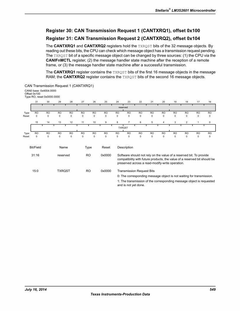
Register 30: CAN Transmission Request 1 (CANTXRQ1), offset 0x100Register 31: CAN Transmission Request 2 (CANTXRQ2), offset 0x104The CANTXRQ1 and CANTXRQ2 registers hold the TXRQST bits of the 32 message objects. Byreading out these bits, the CPU can check whichmessage object has a transmission request pending.The TXRQST bit of a specific message object can be changed by three sources: (1) the CPU via theCANIFnMCTL register, (2) the message handler state machine after the reception of a remoteframe, or (3) the message handler state machine after a successful transmission.
The CANTXRQ1 register contains the TXRQST bits of the first 16 message objects in the messageRAM; the CANTXRQ2 register contains the TXRQST bits of the second 16 message objects.
CAN Transmission Request 1 (CANTXRQ1)CAN0 base: 0x4004.0000Offset 0x100Type RO, reset 0x0000.0000
16171819202122232425262728293031
reserved
ROROROROROROROROROROROROROROROROType0000000000000000Reset
0123456789101112131415
TXRQST
ROROROROROROROROROROROROROROROROType0000000000000000Reset
DescriptionResetTypeNameBit/Field
Software should not rely on the value of a reserved bit. To providecompatibility with future products, the value of a reserved bit should bepreserved across a read-modify-write operation.
0x0000ROreserved31:16
Transmission Request Bits0: The corresponding message object is not waiting for transmission.1: The transmission of the corresponding message object is requestedand is not yet done.
0x0000ROTXRQST15:0
549July 16, 2014Texas Instruments-Production Data
Stellaris® LM3S2601 Microcontroller
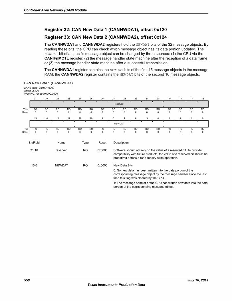
Register 32: CAN New Data 1 (CANNWDA1), offset 0x120Register 33: CAN New Data 2 (CANNWDA2), offset 0x124The CANNWDA1 and CANNWDA2 registers hold the NEWDAT bits of the 32 message objects. Byreading these bits, the CPU can check which message object has its data portion updated. TheNEWDAT bit of a specific message object can be changed by three sources: (1) the CPU via theCANIFnMCTL register, (2) the message handler state machine after the reception of a data frame,or (3) the message handler state machine after a successful transmission.
The CANNWDA1 register contains the NEWDAT bits of the first 16 message objects in the messageRAM; the CANNWDA2 register contains the NEWDAT bits of the second 16 message objects.
CAN New Data 1 (CANNWDA1)CAN0 base: 0x4004.0000Offset 0x120Type RO, reset 0x0000.0000
16171819202122232425262728293031
reserved
ROROROROROROROROROROROROROROROROType0000000000000000Reset
0123456789101112131415
NEWDAT
ROROROROROROROROROROROROROROROROType0000000000000000Reset
DescriptionResetTypeNameBit/Field
Software should not rely on the value of a reserved bit. To providecompatibility with future products, the value of a reserved bit should bepreserved across a read-modify-write operation.
0x0000ROreserved31:16
New Data Bits0: No new data has been written into the data portion of thecorresponding message object by the message handler since the lasttime this flag was cleared by the CPU.1: The message handler or the CPU has written new data into the dataportion of the corresponding message object.
0x0000RONEWDAT15:0
July 16, 2014550Texas Instruments-Production Data
Controller Area Network (CAN) Module

Register 34: CAN Message 1 Interrupt Pending (CANMSG1INT), offset 0x140Register 35: CAN Message 2 Interrupt Pending (CANMSG2INT), offset 0x144The CANMSG1INT and CANMSG2INT registers hold the INTPND bits of the 32 message objects.By reading these bits, the CPU can check which message object has an interrupt pending. TheINTPND bit of a specific message object can be changed through two sources: (1) the CPU via theCANIFnMCTL register, or (2) the message handler state machine after the reception or transmissionof a frame.
This field is also encoded in the CANINT register.
TheCANMSG1INT register contains the INTPND bits of the first 16 message objects in the messageRAM; the CANMSG2INT register contains the INTPND bits of the second 16 message objects.
CAN Message 1 Interrupt Pending (CANMSG1INT)CAN0 base: 0x4004.0000Offset 0x140Type RO, reset 0x0000.0000
16171819202122232425262728293031
reserved
ROROROROROROROROROROROROROROROROType0000000000000000Reset
0123456789101112131415
INTPND
ROROROROROROROROROROROROROROROROType0000000000000000Reset
DescriptionResetTypeNameBit/Field
Software should not rely on the value of a reserved bit. To providecompatibility with future products, the value of a reserved bit should bepreserved across a read-modify-write operation.
0x0000ROreserved31:16
Interrupt Pending Bits0: The corresponding message object is not the source of an interrupt.1: The corresponding message object is the source of an interrupt.
0x0000ROINTPND15:0
551July 16, 2014Texas Instruments-Production Data
Stellaris® LM3S2601 Microcontroller
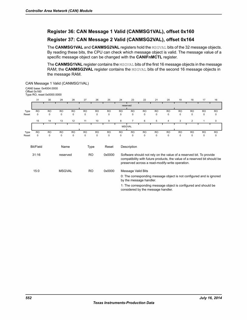
Register 36: CAN Message 1 Valid (CANMSG1VAL), offset 0x160Register 37: CAN Message 2 Valid (CANMSG2VAL), offset 0x164The CANMSG1VAL and CANMSG2VAL registers hold the MSGVAL bits of the 32 message objects.By reading these bits, the CPU can check which message object is valid. The message value of aspecific message object can be changed with the CANIFnMCTL register.
TheCANMSG1VAL register contains the MSGVAL bits of the first 16 message objects in the messageRAM; the CANMSG2VAL register contains the MSGVAL bits of the second 16 message objects inthe message RAM.
CAN Message 1 Valid (CANMSG1VAL)CAN0 base: 0x4004.0000Offset 0x160Type RO, reset 0x0000.0000
16171819202122232425262728293031
reserved
ROROROROROROROROROROROROROROROROType0000000000000000Reset
0123456789101112131415
MSGVAL
ROROROROROROROROROROROROROROROROType0000000000000000Reset
DescriptionResetTypeNameBit/Field
Software should not rely on the value of a reserved bit. To providecompatibility with future products, the value of a reserved bit should bepreserved across a read-modify-write operation.
0x0000ROreserved31:16
Message Valid Bits0: The corresponding message object is not configured and is ignoredby the message handler.1: The corresponding message object is configured and should beconsidered by the message handler.
0x0000ROMSGVAL15:0
July 16, 2014552Texas Instruments-Production Data
Controller Area Network (CAN) Module
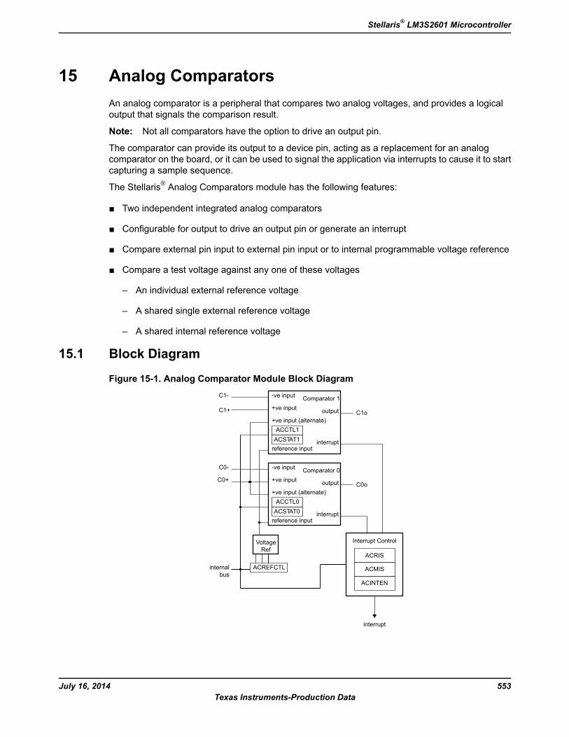
15 Analog ComparatorsAn analog comparator is a peripheral that compares two analog voltages, and provides a logicaloutput that signals the comparison result.
Note: Not all comparators have the option to drive an output pin.
The comparator can provide its output to a device pin, acting as a replacement for an analogcomparator on the board, or it can be used to signal the application via interrupts to cause it to startcapturing a sample sequence.
The Stellaris® Analog Comparators module has the following features:
Two independent integrated analog comparators
Configurable for output to drive an output pin or generate an interrupt
Compare external pin input to external pin input or to internal programmable voltage reference
Compare a test voltage against any one of these voltages
– An individual external reference voltage
– A shared single external reference voltage
– A shared internal reference voltage
15.1 Block Diagram
Figure 15-1. Analog Comparator Module Block Diagram
VoltageRef
ACREFCTL
output+ve input (alternate)
+ve input
interrupt
-ve input
reference input
Comparator 0
ACSTAT0ACCTL0
C0+
internalbus
C0-
C0o
C1-
C1+ output+ve input (alternate)
+ve input
interrupt
-ve input
reference input
Comparator 1
ACSTAT1ACCTL1
C1o
Interrupt Control
ACRIS
ACMIS
ACINTEN
interrupt
553July 16, 2014Texas Instruments-Production Data
Stellaris® LM3S2601 Microcontroller
15.2 Signal DescriptionTable 15-1 on page 554 and Table 15-2 on page 554 list the external signals of the Analog Comparatorsand describe the function of each. The Analog Comparator output signals are alternate functionsfor some GPIO signals and default to be GPIO signals at reset. The column in the table below titled"Pin Assignment" lists the possible GPIO pin placements for the Analog Comparator signals. TheAFSEL bit in theGPIO Alternate Function Select (GPIOAFSEL) register (page 302) should be setto choose the Analog Comparator function. The positive and negative input signals are configuredby clearing the DEN bit in the GPIO Digital Enable (GPIODEN) register. For more information onconfiguring GPIOs, see “General-Purpose Input/Outputs (GPIOs)” on page 279.
Table 15-1. Analog Comparators Signals (100LQFP)
DescriptionBuffer TypeaPin TypePin NumberPin Name
Analog comparator 0 positive input.AnalogI90C0+
Analog comparator 0 negative input.AnalogI92C0-
Analog comparator 0 output.TTLO58C0o
Analog comparator 1 positive input.AnalogI24C1+
Analog comparator 1 negative input.AnalogI91C1-
Analog comparator 1 output.TTLO2C1o
a. The TTL designation indicates the pin has TTL-compatible voltage levels.
Table 15-2. Analog Comparators Signals (108BGA)
DescriptionBuffer TypeaPin TypePin NumberPin Name
Analog comparator 0 positive input.AnalogIA7C0+
Analog comparator 0 negative input.AnalogIA6C0-
Analog comparator 0 output.TTLOL9C0o
Analog comparator 1 positive input.AnalogIM1C1+
Analog comparator 1 negative input.AnalogIB7C1-
Analog comparator 1 output.TTLOC2C1o
a. The TTL designation indicates the pin has TTL-compatible voltage levels.
15.3 Functional DescriptionImportant: It is recommended that the Digital-Input enable (the GPIODEN bit in the GPIO module)
for the analog input pin be disabled to prevent excessive current draw from the I/Opads.
The comparator compares the VIN- and VIN+ inputs to produce an output, VOUT.
VIN- < VIN+, VOUT = 1VIN- > VIN+, VOUT = 0
As shown in Figure 15-2 on page 555, the input source for VIN- is an external input. In addition toan external input, input sources for VIN+ can be the +ve input of comparator 0 or an internal reference.
July 16, 2014554Texas Instruments-Production Data
Analog Comparators
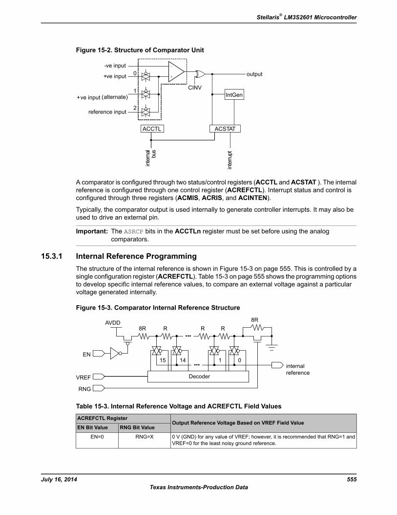
Figure 15-2. Structure of Comparator Unit
output
reference input
ACCTL
IntGen
2
1
0
CINV
interrupt
internal
bus
ACSTAT
(alternate)+ve input
+ve input
-ve input
A comparator is configured through two status/control registers (ACCTL andACSTAT ). The internalreference is configured through one control register (ACREFCTL). Interrupt status and control isconfigured through three registers (ACMIS, ACRIS, and ACINTEN).
Typically, the comparator output is used internally to generate controller interrupts. It may also beused to drive an external pin.
Important: The ASRCP bits in the ACCTLn register must be set before using the analogcomparators.
15.3.1 Internal Reference ProgrammingThe structure of the internal reference is shown in Figure 15-3 on page 555. This is controlled by asingle configuration register (ACREFCTL). Table 15-3 on page 555 shows the programming optionsto develop specific internal reference values, to compare an external voltage against a particularvoltage generated internally.
Figure 15-3. Comparator Internal Reference Structure
8R R R8R
R•••
•••0
Decoder
115 14
AVDD
EN
internalreference
VREF
RNG
Table 15-3. Internal Reference Voltage and ACREFCTL Field Values
Output Reference Voltage Based on VREF Field ValueACREFCTL Register
RNG Bit ValueEN Bit Value
0 V (GND) for any value of VREF; however, it is recommended that RNG=1 andVREF=0 for the least noisy ground reference.
RNG=XEN=0
555July 16, 2014Texas Instruments-Production Data
Stellaris® LM3S2601 Microcontroller
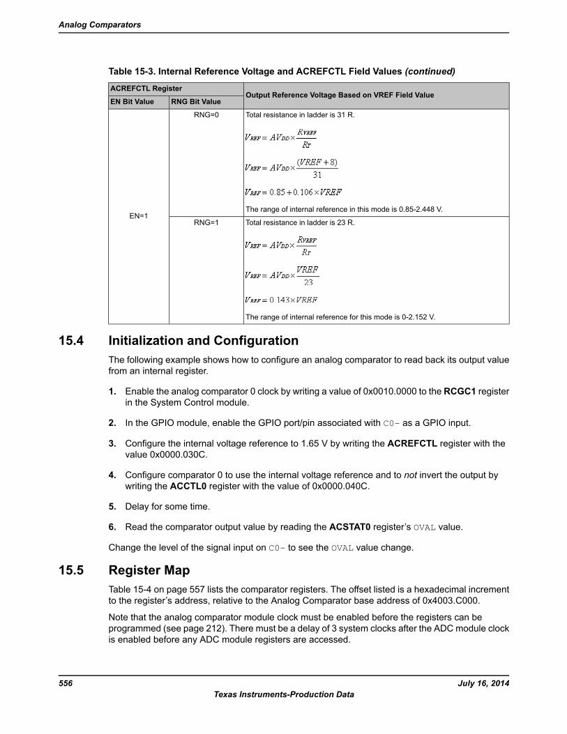
Table 15-3. Internal Reference Voltage and ACREFCTL Field Values (continued)
Output Reference Voltage Based on VREF Field ValueACREFCTL Register
RNG Bit ValueEN Bit Value
Total resistance in ladder is 31 R.
The range of internal reference in this mode is 0.85-2.448 V.
RNG=0
EN=1Total resistance in ladder is 23 R.
The range of internal reference for this mode is 0-2.152 V.
RNG=1
15.4 Initialization and ConfigurationThe following example shows how to configure an analog comparator to read back its output valuefrom an internal register.
1. Enable the analog comparator 0 clock by writing a value of 0x0010.0000 to the RCGC1 registerin the System Control module.
2. In the GPIO module, enable the GPIO port/pin associated with C0- as a GPIO input.
3. Configure the internal voltage reference to 1.65 V by writing the ACREFCTL register with thevalue 0x0000.030C.
4. Configure comparator 0 to use the internal voltage reference and to not invert the output bywriting the ACCTL0 register with the value of 0x0000.040C.
5. Delay for some time.
6. Read the comparator output value by reading the ACSTAT0 register’s OVAL value.
Change the level of the signal input on C0- to see the OVAL value change.
15.5 Register MapTable 15-4 on page 557 lists the comparator registers. The offset listed is a hexadecimal incrementto the register’s address, relative to the Analog Comparator base address of 0x4003.C000.
Note that the analog comparator module clock must be enabled before the registers can beprogrammed (see page 212). There must be a delay of 3 system clocks after the ADCmodule clockis enabled before any ADC module registers are accessed.
July 16, 2014556Texas Instruments-Production Data
Analog Comparators
Table 15-4. Analog Comparators Register Map
SeepageDescriptionResetTypeNameOffset
558Analog Comparator Masked Interrupt Status0x0000.0000R/W1CACMIS0x000
559Analog Comparator Raw Interrupt Status0x0000.0000ROACRIS0x004
560Analog Comparator Interrupt Enable0x0000.0000R/WACINTEN0x008
561Analog Comparator Reference Voltage Control0x0000.0000R/WACREFCTL0x010
562Analog Comparator Status 00x0000.0000ROACSTAT00x020
563Analog Comparator Control 00x0000.0000R/WACCTL00x024
562Analog Comparator Status 10x0000.0000ROACSTAT10x040
563Analog Comparator Control 10x0000.0000R/WACCTL10x044
15.6 Register DescriptionsThe remainder of this section lists and describes the Analog Comparator registers, in numericalorder by address offset.
557July 16, 2014Texas Instruments-Production Data
Stellaris® LM3S2601 Microcontroller
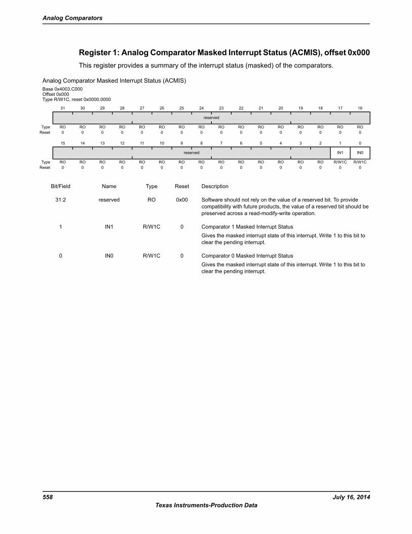
Register 1: Analog Comparator Masked Interrupt Status (ACMIS), offset 0x000This register provides a summary of the interrupt status (masked) of the comparators.
Analog Comparator Masked Interrupt Status (ACMIS)Base 0x4003.C000Offset 0x000Type R/W1C, reset 0x0000.0000
16171819202122232425262728293031
reserved
ROROROROROROROROROROROROROROROROType0000000000000000Reset
0123456789101112131415
IN0IN1reserved
R/W1CR/W1CROROROROROROROROROROROROROROType0000000000000000Reset
DescriptionResetTypeNameBit/Field
Software should not rely on the value of a reserved bit. To providecompatibility with future products, the value of a reserved bit should bepreserved across a read-modify-write operation.
0x00ROreserved31:2
Comparator 1 Masked Interrupt StatusGives the masked interrupt state of this interrupt. Write 1 to this bit toclear the pending interrupt.
0R/W1CIN11
Comparator 0 Masked Interrupt StatusGives the masked interrupt state of this interrupt. Write 1 to this bit toclear the pending interrupt.
0R/W1CIN00
July 16, 2014558Texas Instruments-Production Data
Analog Comparators
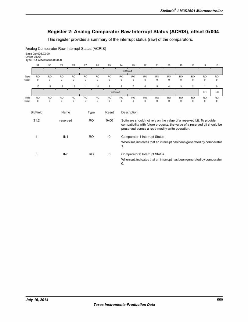
Register 2: Analog Comparator Raw Interrupt Status (ACRIS), offset 0x004This register provides a summary of the interrupt status (raw) of the comparators.
Analog Comparator Raw Interrupt Status (ACRIS)Base 0x4003.C000Offset 0x004Type RO, reset 0x0000.0000
16171819202122232425262728293031
reserved
ROROROROROROROROROROROROROROROROType0000000000000000Reset
0123456789101112131415
IN0IN1reserved
ROROROROROROROROROROROROROROROROType0000000000000000Reset
DescriptionResetTypeNameBit/Field
Software should not rely on the value of a reserved bit. To providecompatibility with future products, the value of a reserved bit should bepreserved across a read-modify-write operation.
0x00ROreserved31:2
Comparator 1 Interrupt StatusWhen set, indicates that an interrupt has been generated by comparator1.
0ROIN11
Comparator 0 Interrupt StatusWhen set, indicates that an interrupt has been generated by comparator0.
0ROIN00
559July 16, 2014Texas Instruments-Production Data
Stellaris® LM3S2601 Microcontroller
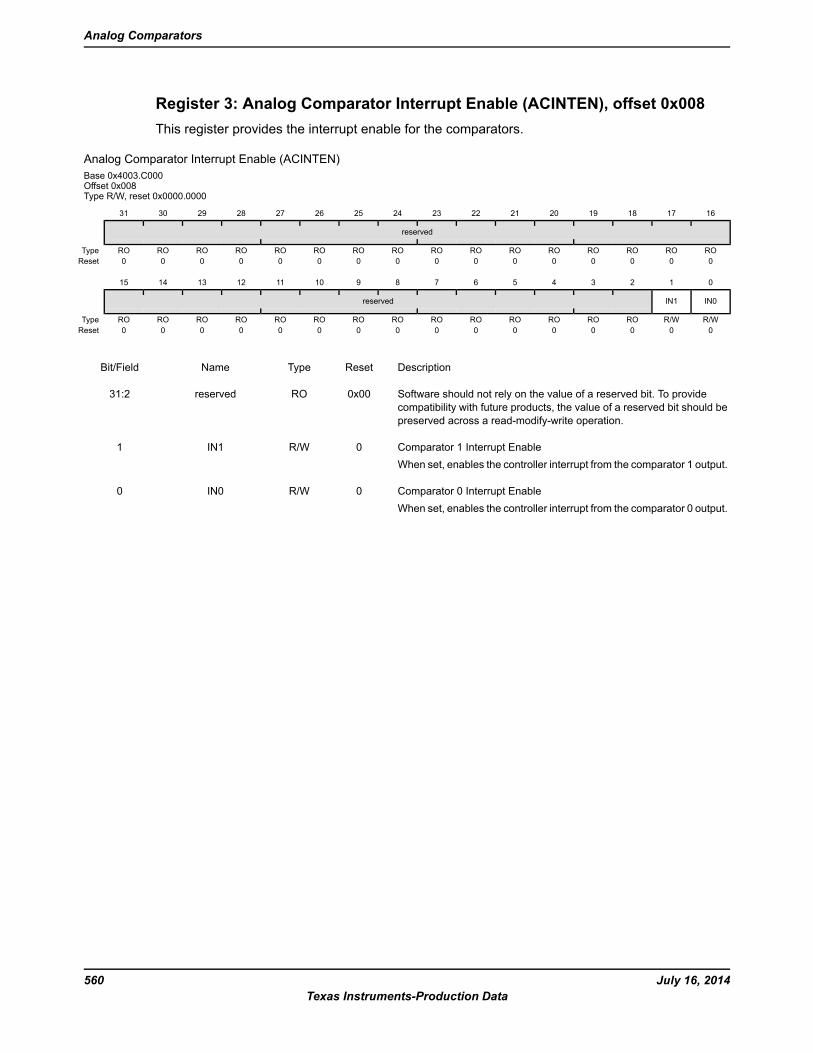
Register 3: Analog Comparator Interrupt Enable (ACINTEN), offset 0x008This register provides the interrupt enable for the comparators.
Analog Comparator Interrupt Enable (ACINTEN)Base 0x4003.C000Offset 0x008Type R/W, reset 0x0000.0000
16171819202122232425262728293031
reserved
ROROROROROROROROROROROROROROROROType0000000000000000Reset
0123456789101112131415
IN0IN1reserved
R/WR/WROROROROROROROROROROROROROROType0000000000000000Reset
DescriptionResetTypeNameBit/Field
Software should not rely on the value of a reserved bit. To providecompatibility with future products, the value of a reserved bit should bepreserved across a read-modify-write operation.
0x00ROreserved31:2
Comparator 1 Interrupt EnableWhen set, enables the controller interrupt from the comparator 1 output.
0R/WIN11
Comparator 0 Interrupt EnableWhen set, enables the controller interrupt from the comparator 0 output.
0R/WIN00
July 16, 2014560Texas Instruments-Production Data
Analog Comparators
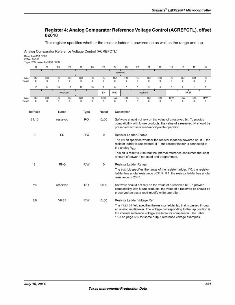
Register 4: Analog Comparator Reference Voltage Control (ACREFCTL), offset0x010This register specifies whether the resistor ladder is powered on as well as the range and tap.
Analog Comparator Reference Voltage Control (ACREFCTL)Base 0x4003.C000Offset 0x010Type R/W, reset 0x0000.0000
16171819202122232425262728293031
reserved
ROROROROROROROROROROROROROROROROType0000000000000000Reset
0123456789101112131415
VREFreservedRNGENreserved
R/WR/WR/WR/WROROROROR/WR/WROROROROROROType0000000000000000Reset
DescriptionResetTypeNameBit/Field
Software should not rely on the value of a reserved bit. To providecompatibility with future products, the value of a reserved bit should bepreserved across a read-modify-write operation.
0x00ROreserved31:10
Resistor Ladder EnableThe EN bit specifies whether the resistor ladder is powered on. If 0, theresistor ladder is unpowered. If 1, the resistor ladder is connected tothe analog VDD.
This bit is reset to 0 so that the internal reference consumes the leastamount of power if not used and programmed.
0R/WEN9
Resistor Ladder RangeThe RNG bit specifies the range of the resistor ladder. If 0, the resistorladder has a total resistance of 31 R. If 1, the resistor ladder has a totalresistance of 23 R.
0R/WRNG8
Software should not rely on the value of a reserved bit. To providecompatibility with future products, the value of a reserved bit should bepreserved across a read-modify-write operation.
0x00ROreserved7:4
Resistor Ladder Voltage RefThe VREF bit field specifies the resistor ladder tap that is passed throughan analog multiplexer. The voltage corresponding to the tap position isthe internal reference voltage available for comparison. See Table15-3 on page 555 for some output reference voltage examples.
0x00R/WVREF3:0
561July 16, 2014Texas Instruments-Production Data
Stellaris® LM3S2601 Microcontroller
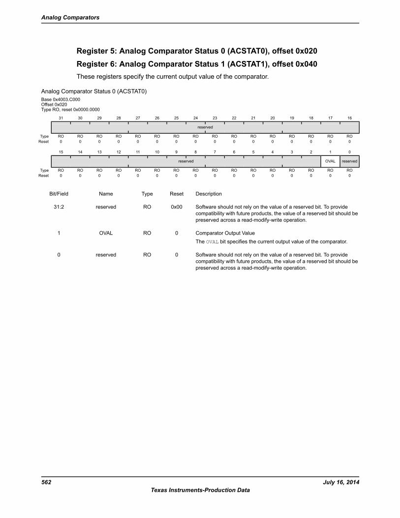
Register 5: Analog Comparator Status 0 (ACSTAT0), offset 0x020Register 6: Analog Comparator Status 1 (ACSTAT1), offset 0x040These registers specify the current output value of the comparator.
Analog Comparator Status 0 (ACSTAT0)Base 0x4003.C000Offset 0x020Type RO, reset 0x0000.0000
16171819202122232425262728293031
reserved
ROROROROROROROROROROROROROROROROType0000000000000000Reset
0123456789101112131415
reservedOVALreserved
ROROROROROROROROROROROROROROROROType0000000000000000Reset
DescriptionResetTypeNameBit/Field
Software should not rely on the value of a reserved bit. To providecompatibility with future products, the value of a reserved bit should bepreserved across a read-modify-write operation.
0x00ROreserved31:2
Comparator Output ValueThe OVAL bit specifies the current output value of the comparator.
0ROOVAL1
Software should not rely on the value of a reserved bit. To providecompatibility with future products, the value of a reserved bit should bepreserved across a read-modify-write operation.
0ROreserved0
July 16, 2014562Texas Instruments-Production Data
Analog Comparators
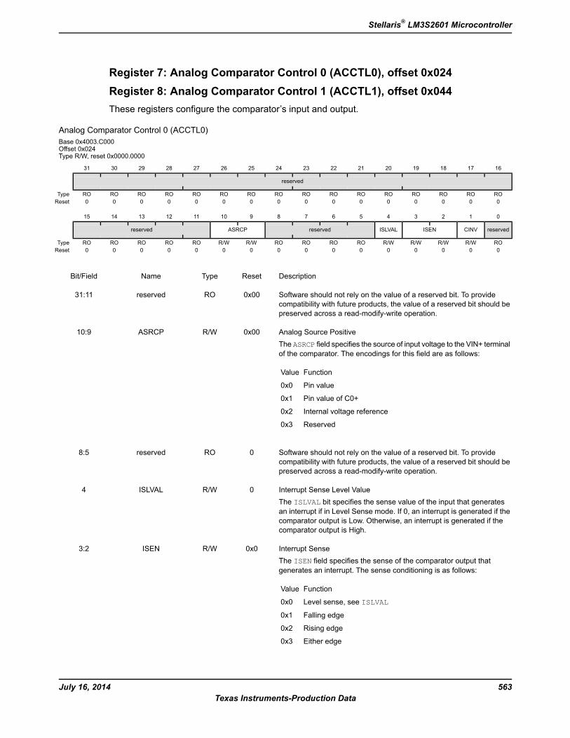
Register 7: Analog Comparator Control 0 (ACCTL0), offset 0x024Register 8: Analog Comparator Control 1 (ACCTL1), offset 0x044These registers configure the comparator’s input and output.
Analog Comparator Control 0 (ACCTL0)Base 0x4003.C000Offset 0x024Type R/W, reset 0x0000.0000
16171819202122232425262728293031
reserved
ROROROROROROROROROROROROROROROROType0000000000000000Reset
0123456789101112131415
reservedCINVISENISLVALreservedASRCPreserved
ROR/WR/WR/WR/WROROROROR/WR/WROROROROROType0000000000000000Reset
DescriptionResetTypeNameBit/Field
Software should not rely on the value of a reserved bit. To providecompatibility with future products, the value of a reserved bit should bepreserved across a read-modify-write operation.
0x00ROreserved31:11
Analog Source PositiveThe ASRCP field specifies the source of input voltage to the VIN+ terminalof the comparator. The encodings for this field are as follows:
FunctionValue
Pin value0x0
Pin value of C0+0x1
Internal voltage reference0x2
Reserved0x3
0x00R/WASRCP10:9
Software should not rely on the value of a reserved bit. To providecompatibility with future products, the value of a reserved bit should bepreserved across a read-modify-write operation.
0ROreserved8:5
Interrupt Sense Level ValueThe ISLVAL bit specifies the sense value of the input that generatesan interrupt if in Level Sense mode. If 0, an interrupt is generated if thecomparator output is Low. Otherwise, an interrupt is generated if thecomparator output is High.
0R/WISLVAL4
Interrupt SenseThe ISEN field specifies the sense of the comparator output thatgenerates an interrupt. The sense conditioning is as follows:
FunctionValue
Level sense, see ISLVAL0x0
Falling edge0x1
Rising edge0x2
Either edge0x3
0x0R/WISEN3:2
563July 16, 2014Texas Instruments-Production Data
Stellaris® LM3S2601 Microcontroller
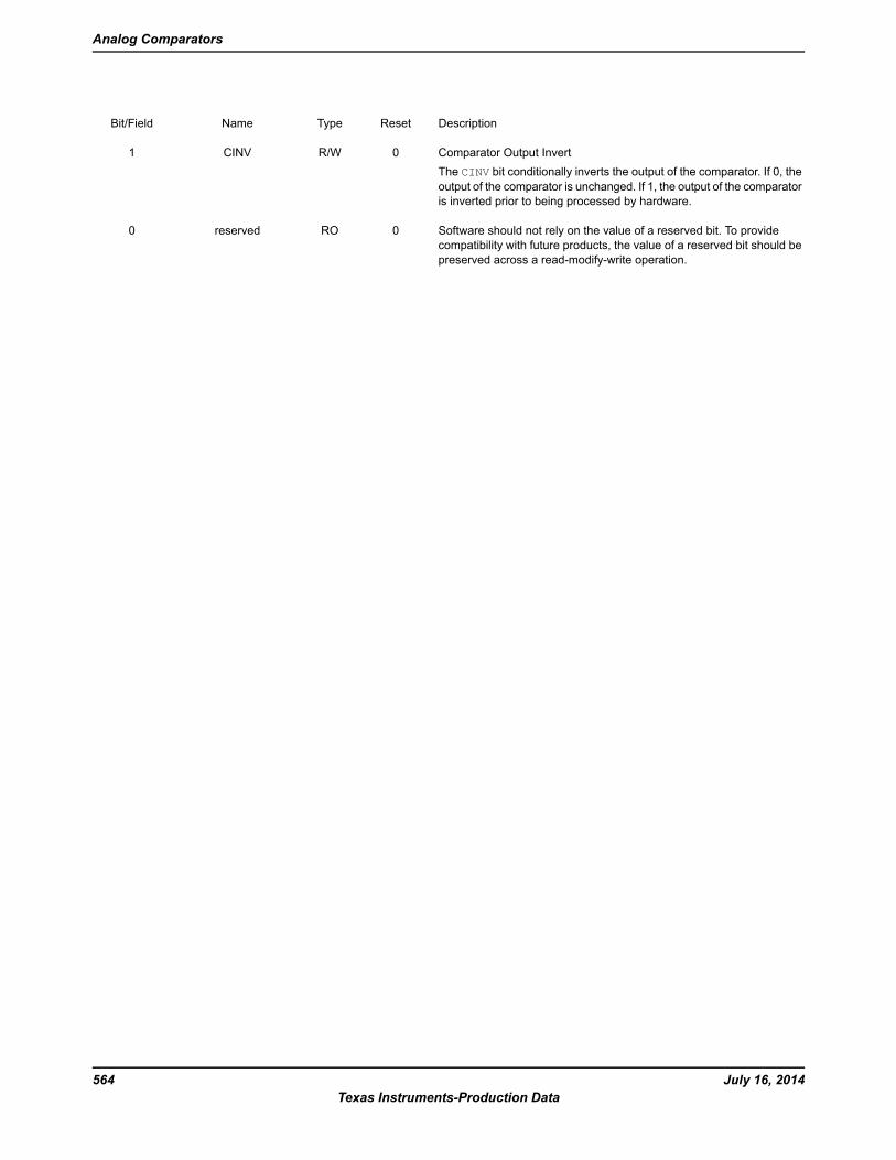
DescriptionResetTypeNameBit/Field
Comparator Output InvertThe CINV bit conditionally inverts the output of the comparator. If 0, theoutput of the comparator is unchanged. If 1, the output of the comparatoris inverted prior to being processed by hardware.
0R/WCINV1
Software should not rely on the value of a reserved bit. To providecompatibility with future products, the value of a reserved bit should bepreserved across a read-modify-write operation.
0ROreserved0
July 16, 2014564Texas Instruments-Production Data
Analog Comparators
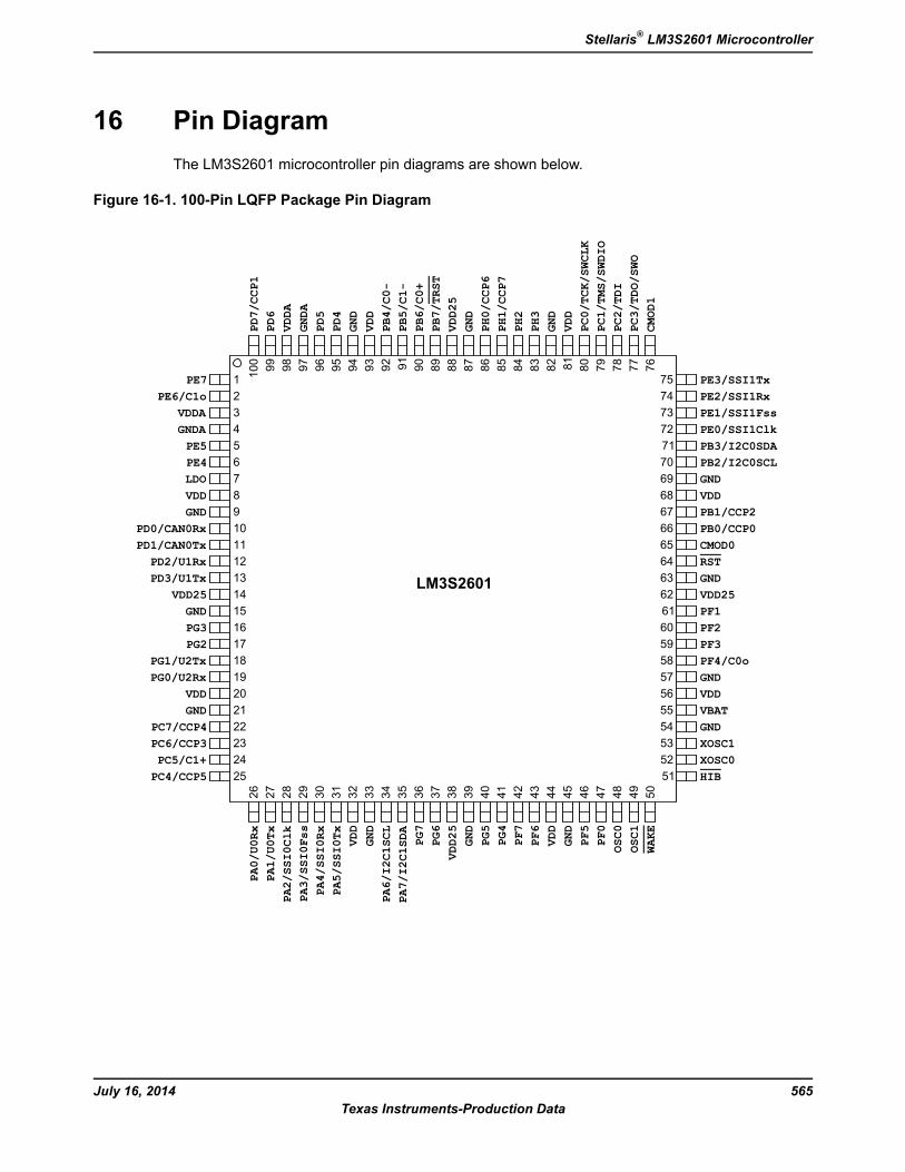
16 Pin DiagramThe LM3S2601 microcontroller pin diagrams are shown below.
Figure 16-1. 100-Pin LQFP Package Pin Diagram
565July 16, 2014Texas Instruments-Production Data
Stellaris® LM3S2601 Microcontroller
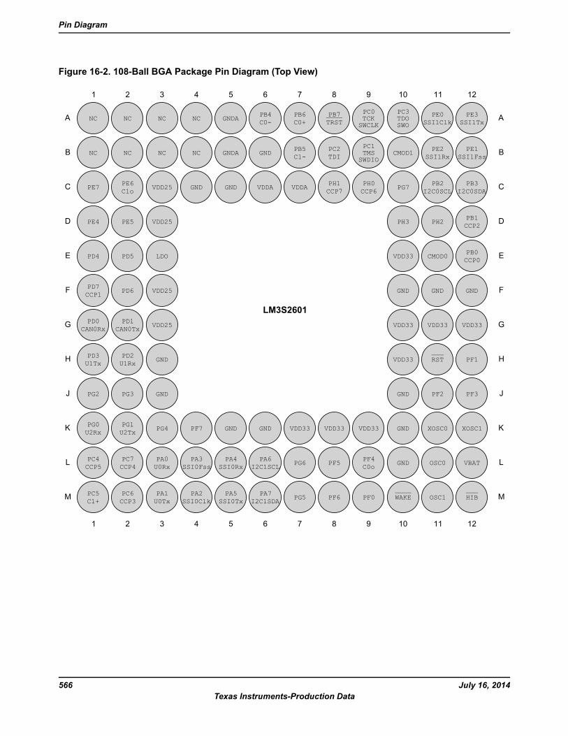
Figure 16-2. 108-Ball BGA Package Pin Diagram (Top View)
July 16, 2014566Texas Instruments-Production Data
Pin Diagram
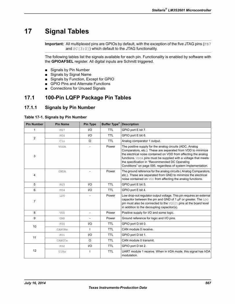
17 Signal TablesImportant: All multiplexed pins are GPIOs by default, with the exception of the five JTAG pins (PB7
and PC[3:0]) which default to the JTAG functionality.
The following tables list the signals available for each pin. Functionality is enabled by software withthe GPIOAFSEL register. All digital inputs are Schmitt triggered.
Signals by Pin Number Signals by Signal Name Signals by Function, Except for GPIO GPIO Pins and Alternate Functions Connections for Unused Signals
17.1 100-Pin LQFP Package Pin Tables
17.1.1 Signals by Pin Number
Table 17-1. Signals by Pin Number
DescriptionBuffer TypeaPin TypePin NamePin Number
GPIO port E bit 7.TTLI/OPE71
GPIO port E bit 6.TTLI/OPE62
Analog comparator 1 output.TTLOC1o
The positive supply for the analog circuits (ADC, AnalogComparators, etc.). These are separated from VDD to minimizethe electrical noise contained on VDD from affecting the analogfunctions. VDDA pins must be supplied with a voltage that meetsthe specification in “Recommended DC OperatingConditions” on page 595, regardless of system implementation.
Power-VDDA
3
The ground reference for the analog circuits ( Analog Comparators,etc.). These are separated from GND to minimize the electricalnoise contained on VDD from affecting the analog functions.
Power-GNDA4
GPIO port E bit 5.TTLI/OPE55
GPIO port E bit 4.TTLI/OPE46
Low drop-out regulator output voltage. This pin requires an externalcapacitor between the pin and GND of 1 µF or greater. The LDOpin must also be connected to the VDD25 pins at the board levelin addition to the decoupling capacitor(s).
Power-LDO
7
Positive supply for I/O and some logic.Power-VDD8
Ground reference for logic and I/O pins.Power-GND9
GPIO port D bit 0.TTLI/OPD010
CAN module 0 receive.TTLICAN0Rx
GPIO port D bit 1.TTLI/OPD111
CAN module 0 transmit.TTLOCAN0Tx
GPIO port D bit 2.TTLI/OPD2
12 UART module 1 receive. When in IrDA mode, this signal has IrDAmodulation.
TTLIU1Rx
567July 16, 2014Texas Instruments-Production Data
Stellaris® LM3S2601 Microcontroller
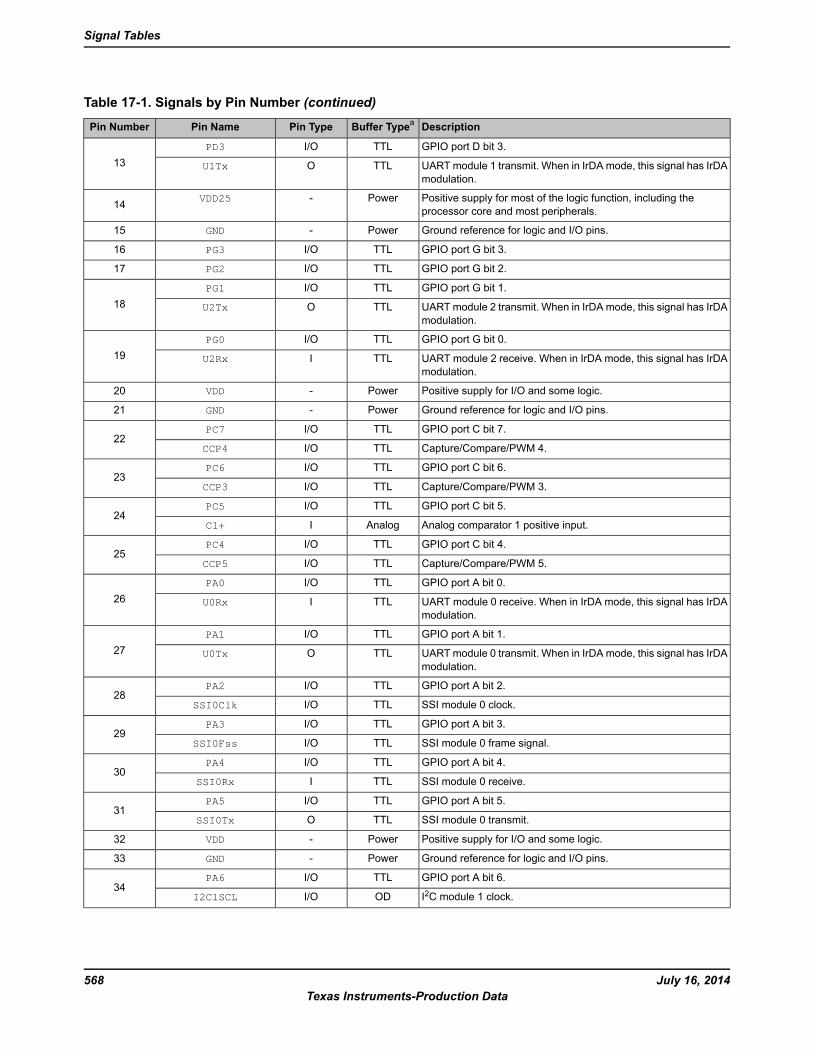
Table 17-1. Signals by Pin Number (continued)
DescriptionBuffer TypeaPin TypePin NamePin Number
GPIO port D bit 3.TTLI/OPD3
13 UARTmodule 1 transmit. When in IrDA mode, this signal has IrDAmodulation.
TTLOU1Tx
Positive supply for most of the logic function, including theprocessor core and most peripherals.
Power-VDD2514
Ground reference for logic and I/O pins.Power-GND15
GPIO port G bit 3.TTLI/OPG316
GPIO port G bit 2.TTLI/OPG217
GPIO port G bit 1.TTLI/OPG1
18 UARTmodule 2 transmit. When in IrDA mode, this signal has IrDAmodulation.
TTLOU2Tx
GPIO port G bit 0.TTLI/OPG0
19 UART module 2 receive. When in IrDA mode, this signal has IrDAmodulation.
TTLIU2Rx
Positive supply for I/O and some logic.Power-VDD20
Ground reference for logic and I/O pins.Power-GND21
GPIO port C bit 7.TTLI/OPC722
Capture/Compare/PWM 4.TTLI/OCCP4
GPIO port C bit 6.TTLI/OPC623
Capture/Compare/PWM 3.TTLI/OCCP3
GPIO port C bit 5.TTLI/OPC524
Analog comparator 1 positive input.AnalogIC1+
GPIO port C bit 4.TTLI/OPC425
Capture/Compare/PWM 5.TTLI/OCCP5
GPIO port A bit 0.TTLI/OPA0
26 UART module 0 receive. When in IrDA mode, this signal has IrDAmodulation.
TTLIU0Rx
GPIO port A bit 1.TTLI/OPA1
27 UARTmodule 0 transmit. When in IrDA mode, this signal has IrDAmodulation.
TTLOU0Tx
GPIO port A bit 2.TTLI/OPA228
SSI module 0 clock.TTLI/OSSI0Clk
GPIO port A bit 3.TTLI/OPA329
SSI module 0 frame signal.TTLI/OSSI0Fss
GPIO port A bit 4.TTLI/OPA430
SSI module 0 receive.TTLISSI0Rx
GPIO port A bit 5.TTLI/OPA531
SSI module 0 transmit.TTLOSSI0Tx
Positive supply for I/O and some logic.Power-VDD32
Ground reference for logic and I/O pins.Power-GND33
GPIO port A bit 6.TTLI/OPA634
I2C module 1 clock.ODI/OI2C1SCL
July 16, 2014568Texas Instruments-Production Data
Signal Tables
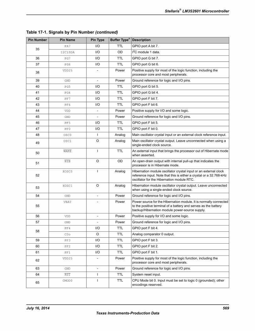
Table 17-1. Signals by Pin Number (continued)
DescriptionBuffer TypeaPin TypePin NamePin Number
GPIO port A bit 7.TTLI/OPA735
I2C module 1 data.ODI/OI2C1SDA
GPIO port G bit 7.TTLI/OPG736
GPIO port G bit 6.TTLI/OPG637
Positive supply for most of the logic function, including theprocessor core and most peripherals.
Power-VDD2538
Ground reference for logic and I/O pins.Power-GND39
GPIO port G bit 5.TTLI/OPG540
GPIO port G bit 4.TTLI/OPG441
GPIO port F bit 7.TTLI/OPF742
GPIO port F bit 6.TTLI/OPF643
Positive supply for I/O and some logic.Power-VDD44
Ground reference for logic and I/O pins.Power-GND45
GPIO port F bit 5.TTLI/OPF546
GPIO port F bit 0.TTLI/OPF047
Main oscillator crystal input or an external clock reference input.AnalogIOSC048
Main oscillator crystal output. Leave unconnected when using asingle-ended clock source.
AnalogOOSC149
An external input that brings the processor out of Hibernate modewhen asserted.
TTLIWAKE50
An open-drain output with internal pull-up that indicates theprocessor is in Hibernate mode.
ODOHIB51
Hibernation module oscillator crystal input or an external clockreference input. Note that this is either a crystal or a 32.768-kHzoscillator for the Hibernation module RTC.
AnalogIXOSC052
Hibernation module oscillator crystal output. Leave unconnectedwhen using a single-ended clock source.
AnalogOXOSC153
Ground reference for logic and I/O pins.Power-GND54
Power source for the Hibernation module. It is normally connectedto the positive terminal of a battery and serves as the batterybackup/Hibernation module power-source supply.
Power-VBAT55
Positive supply for I/O and some logic.Power-VDD56
Ground reference for logic and I/O pins.Power-GND57
GPIO port F bit 4.TTLI/OPF458
Analog comparator 0 output.TTLOC0o
GPIO port F bit 3.TTLI/OPF359
GPIO port F bit 2.TTLI/OPF260
GPIO port F bit 1.TTLI/OPF161
Positive supply for most of the logic function, including theprocessor core and most peripherals.
Power-VDD2562
Ground reference for logic and I/O pins.Power-GND63
System reset input.TTLIRST64
CPU Mode bit 0. Input must be set to logic 0 (grounded); otherencodings reserved.
TTLICMOD065
569July 16, 2014Texas Instruments-Production Data
Stellaris® LM3S2601 Microcontroller
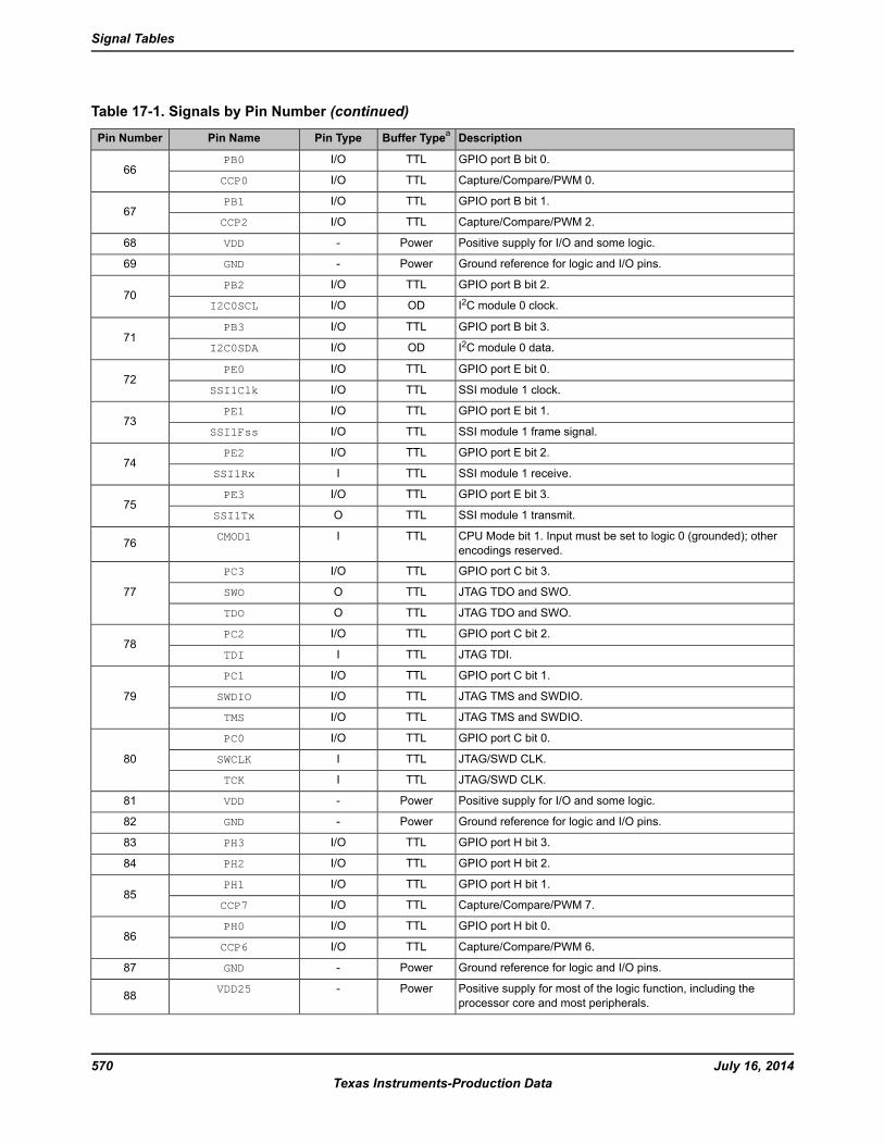
Table 17-1. Signals by Pin Number (continued)
DescriptionBuffer TypeaPin TypePin NamePin Number
GPIO port B bit 0.TTLI/OPB066
Capture/Compare/PWM 0.TTLI/OCCP0
GPIO port B bit 1.TTLI/OPB167
Capture/Compare/PWM 2.TTLI/OCCP2
Positive supply for I/O and some logic.Power-VDD68
Ground reference for logic and I/O pins.Power-GND69
GPIO port B bit 2.TTLI/OPB270
I2C module 0 clock.ODI/OI2C0SCL
GPIO port B bit 3.TTLI/OPB371
I2C module 0 data.ODI/OI2C0SDA
GPIO port E bit 0.TTLI/OPE072
SSI module 1 clock.TTLI/OSSI1Clk
GPIO port E bit 1.TTLI/OPE173
SSI module 1 frame signal.TTLI/OSSI1Fss
GPIO port E bit 2.TTLI/OPE274
SSI module 1 receive.TTLISSI1Rx
GPIO port E bit 3.TTLI/OPE375
SSI module 1 transmit.TTLOSSI1Tx
CPU Mode bit 1. Input must be set to logic 0 (grounded); otherencodings reserved.
TTLICMOD176
GPIO port C bit 3.TTLI/OPC3
77 JTAG TDO and SWO.TTLOSWO
JTAG TDO and SWO.TTLOTDO
GPIO port C bit 2.TTLI/OPC278
JTAG TDI.TTLITDI
GPIO port C bit 1.TTLI/OPC1
79 JTAG TMS and SWDIO.TTLI/OSWDIO
JTAG TMS and SWDIO.TTLI/OTMS
GPIO port C bit 0.TTLI/OPC0
80 JTAG/SWD CLK.TTLISWCLK
JTAG/SWD CLK.TTLITCK
Positive supply for I/O and some logic.Power-VDD81
Ground reference for logic and I/O pins.Power-GND82
GPIO port H bit 3.TTLI/OPH383
GPIO port H bit 2.TTLI/OPH284
GPIO port H bit 1.TTLI/OPH185
Capture/Compare/PWM 7.TTLI/OCCP7
GPIO port H bit 0.TTLI/OPH086
Capture/Compare/PWM 6.TTLI/OCCP6
Ground reference for logic and I/O pins.Power-GND87
Positive supply for most of the logic function, including theprocessor core and most peripherals.
Power-VDD2588
July 16, 2014570Texas Instruments-Production Data
Signal Tables
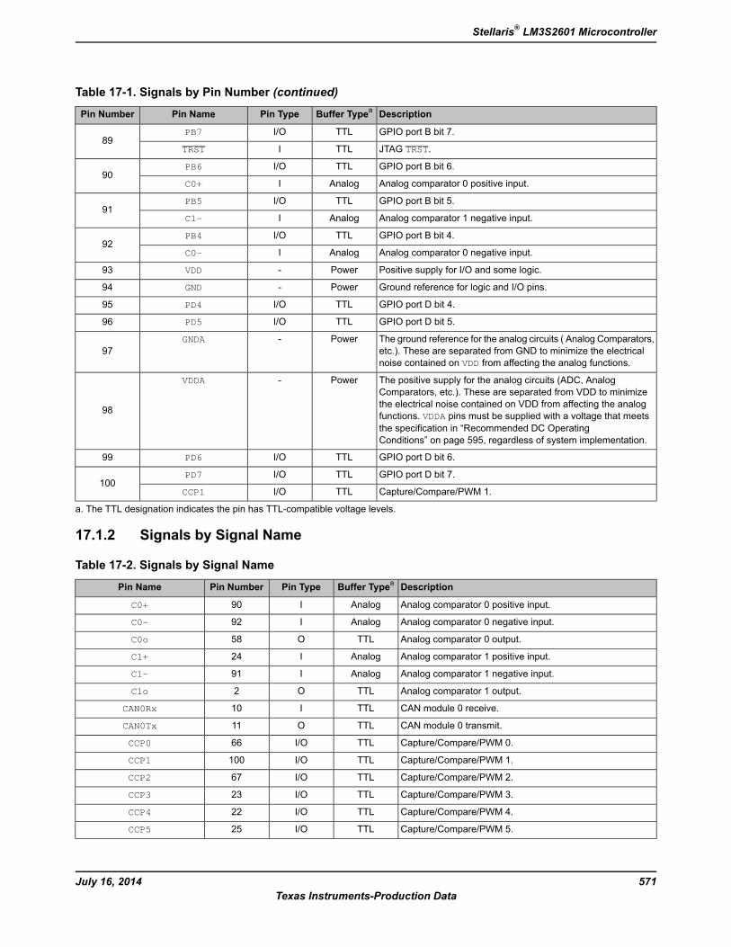
Table 17-1. Signals by Pin Number (continued)
DescriptionBuffer TypeaPin TypePin NamePin Number
GPIO port B bit 7.TTLI/OPB789
JTAG TRST.TTLITRST
GPIO port B bit 6.TTLI/OPB690
Analog comparator 0 positive input.AnalogIC0+
GPIO port B bit 5.TTLI/OPB591
Analog comparator 1 negative input.AnalogIC1-
GPIO port B bit 4.TTLI/OPB492
Analog comparator 0 negative input.AnalogIC0-
Positive supply for I/O and some logic.Power-VDD93
Ground reference for logic and I/O pins.Power-GND94
GPIO port D bit 4.TTLI/OPD495
GPIO port D bit 5.TTLI/OPD596
The ground reference for the analog circuits ( Analog Comparators,etc.). These are separated from GND to minimize the electricalnoise contained on VDD from affecting the analog functions.
Power-GNDA97
The positive supply for the analog circuits (ADC, AnalogComparators, etc.). These are separated from VDD to minimizethe electrical noise contained on VDD from affecting the analogfunctions. VDDA pins must be supplied with a voltage that meetsthe specification in “Recommended DC OperatingConditions” on page 595, regardless of system implementation.
Power-VDDA
98
GPIO port D bit 6.TTLI/OPD699
GPIO port D bit 7.TTLI/OPD7100
Capture/Compare/PWM 1.TTLI/OCCP1
a. The TTL designation indicates the pin has TTL-compatible voltage levels.
17.1.2 Signals by Signal Name
Table 17-2. Signals by Signal Name
DescriptionBuffer TypeaPin TypePin NumberPin Name
Analog comparator 0 positive input.AnalogI90C0+
Analog comparator 0 negative input.AnalogI92C0-
Analog comparator 0 output.TTLO58C0o
Analog comparator 1 positive input.AnalogI24C1+
Analog comparator 1 negative input.AnalogI91C1-
Analog comparator 1 output.TTLO2C1o
CAN module 0 receive.TTLI10CAN0Rx
CAN module 0 transmit.TTLO11CAN0Tx
Capture/Compare/PWM 0.TTLI/O66CCP0
Capture/Compare/PWM 1.TTLI/O100CCP1
Capture/Compare/PWM 2.TTLI/O67CCP2
Capture/Compare/PWM 3.TTLI/O23CCP3
Capture/Compare/PWM 4.TTLI/O22CCP4
Capture/Compare/PWM 5.TTLI/O25CCP5
571July 16, 2014Texas Instruments-Production Data
Stellaris® LM3S2601 Microcontroller
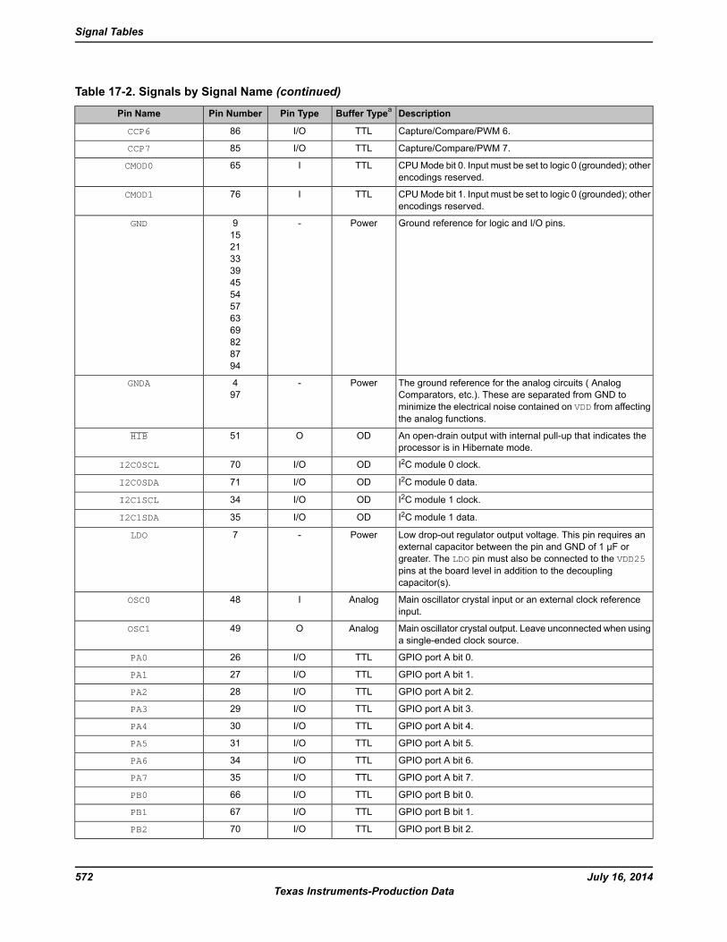
Table 17-2. Signals by Signal Name (continued)
DescriptionBuffer TypeaPin TypePin NumberPin Name
Capture/Compare/PWM 6.TTLI/O86CCP6
Capture/Compare/PWM 7.TTLI/O85CCP7
CPUMode bit 0. Input must be set to logic 0 (grounded); otherencodings reserved.
TTLI65CMOD0
CPUMode bit 1. Input must be set to logic 0 (grounded); otherencodings reserved.
TTLI76CMOD1
Ground reference for logic and I/O pins.Power-9152133394554576369828794
GND
The ground reference for the analog circuits ( AnalogComparators, etc.). These are separated from GND tominimize the electrical noise contained on VDD from affectingthe analog functions.
Power-497
GNDA
An open-drain output with internal pull-up that indicates theprocessor is in Hibernate mode.
ODO51HIB
I2C module 0 clock.ODI/O70I2C0SCL
I2C module 0 data.ODI/O71I2C0SDA
I2C module 1 clock.ODI/O34I2C1SCL
I2C module 1 data.ODI/O35I2C1SDA
Low drop-out regulator output voltage. This pin requires anexternal capacitor between the pin and GND of 1 µF orgreater. The LDO pin must also be connected to the VDD25pins at the board level in addition to the decouplingcapacitor(s).
Power-7LDO
Main oscillator crystal input or an external clock referenceinput.
AnalogI48OSC0
Main oscillator crystal output. Leave unconnected when usinga single-ended clock source.
AnalogO49OSC1
GPIO port A bit 0.TTLI/O26PA0
GPIO port A bit 1.TTLI/O27PA1
GPIO port A bit 2.TTLI/O28PA2
GPIO port A bit 3.TTLI/O29PA3
GPIO port A bit 4.TTLI/O30PA4
GPIO port A bit 5.TTLI/O31PA5
GPIO port A bit 6.TTLI/O34PA6
GPIO port A bit 7.TTLI/O35PA7
GPIO port B bit 0.TTLI/O66PB0
GPIO port B bit 1.TTLI/O67PB1
GPIO port B bit 2.TTLI/O70PB2
July 16, 2014572Texas Instruments-Production Data
Signal Tables
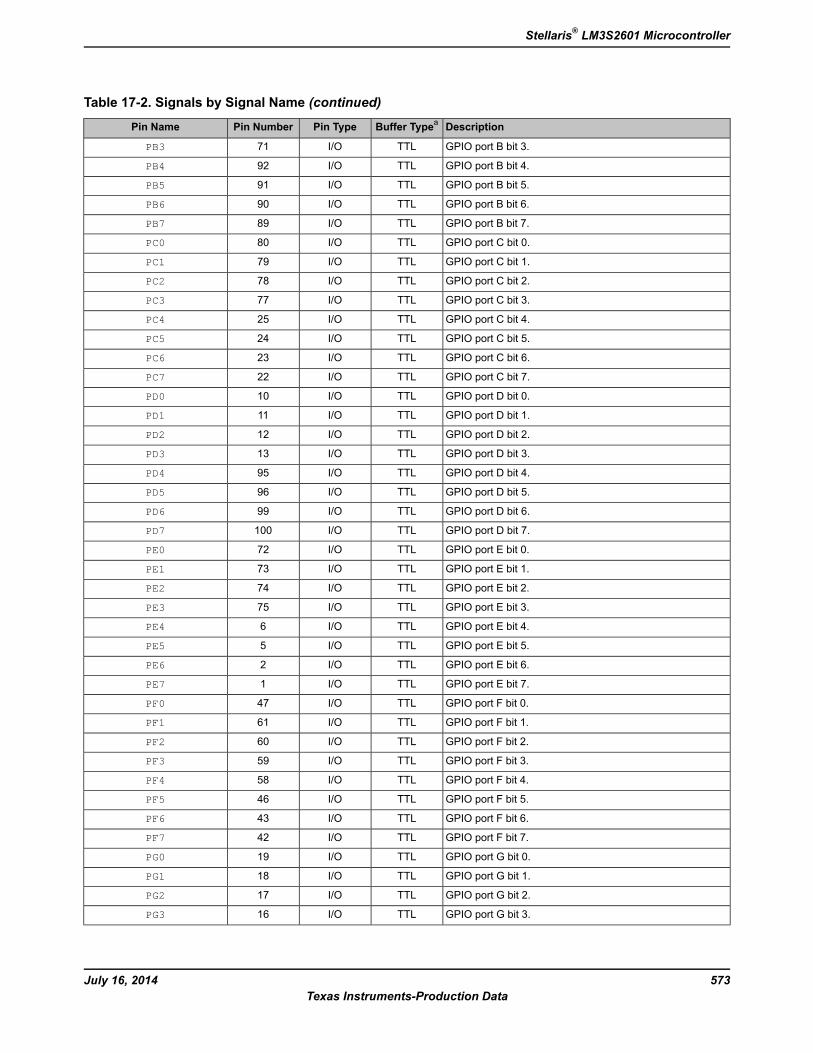
Table 17-2. Signals by Signal Name (continued)
DescriptionBuffer TypeaPin TypePin NumberPin Name
GPIO port B bit 3.TTLI/O71PB3
GPIO port B bit 4.TTLI/O92PB4
GPIO port B bit 5.TTLI/O91PB5
GPIO port B bit 6.TTLI/O90PB6
GPIO port B bit 7.TTLI/O89PB7
GPIO port C bit 0.TTLI/O80PC0
GPIO port C bit 1.TTLI/O79PC1
GPIO port C bit 2.TTLI/O78PC2
GPIO port C bit 3.TTLI/O77PC3
GPIO port C bit 4.TTLI/O25PC4
GPIO port C bit 5.TTLI/O24PC5
GPIO port C bit 6.TTLI/O23PC6
GPIO port C bit 7.TTLI/O22PC7
GPIO port D bit 0.TTLI/O10PD0
GPIO port D bit 1.TTLI/O11PD1
GPIO port D bit 2.TTLI/O12PD2
GPIO port D bit 3.TTLI/O13PD3
GPIO port D bit 4.TTLI/O95PD4
GPIO port D bit 5.TTLI/O96PD5
GPIO port D bit 6.TTLI/O99PD6
GPIO port D bit 7.TTLI/O100PD7
GPIO port E bit 0.TTLI/O72PE0
GPIO port E bit 1.TTLI/O73PE1
GPIO port E bit 2.TTLI/O74PE2
GPIO port E bit 3.TTLI/O75PE3
GPIO port E bit 4.TTLI/O6PE4
GPIO port E bit 5.TTLI/O5PE5
GPIO port E bit 6.TTLI/O2PE6
GPIO port E bit 7.TTLI/O1PE7
GPIO port F bit 0.TTLI/O47PF0
GPIO port F bit 1.TTLI/O61PF1
GPIO port F bit 2.TTLI/O60PF2
GPIO port F bit 3.TTLI/O59PF3
GPIO port F bit 4.TTLI/O58PF4
GPIO port F bit 5.TTLI/O46PF5
GPIO port F bit 6.TTLI/O43PF6
GPIO port F bit 7.TTLI/O42PF7
GPIO port G bit 0.TTLI/O19PG0
GPIO port G bit 1.TTLI/O18PG1
GPIO port G bit 2.TTLI/O17PG2
GPIO port G bit 3.TTLI/O16PG3
573July 16, 2014Texas Instruments-Production Data
Stellaris® LM3S2601 Microcontroller
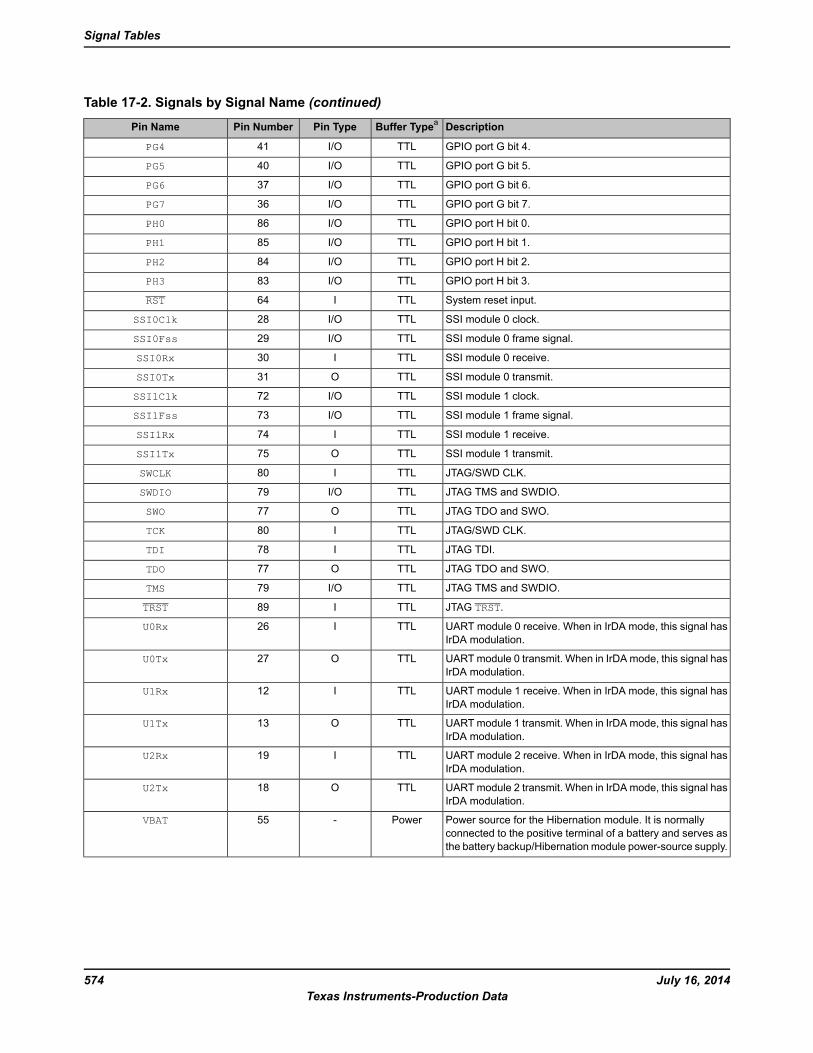
Table 17-2. Signals by Signal Name (continued)
DescriptionBuffer TypeaPin TypePin NumberPin Name
GPIO port G bit 4.TTLI/O41PG4
GPIO port G bit 5.TTLI/O40PG5
GPIO port G bit 6.TTLI/O37PG6
GPIO port G bit 7.TTLI/O36PG7
GPIO port H bit 0.TTLI/O86PH0
GPIO port H bit 1.TTLI/O85PH1
GPIO port H bit 2.TTLI/O84PH2
GPIO port H bit 3.TTLI/O83PH3
System reset input.TTLI64RST
SSI module 0 clock.TTLI/O28SSI0Clk
SSI module 0 frame signal.TTLI/O29SSI0Fss
SSI module 0 receive.TTLI30SSI0Rx
SSI module 0 transmit.TTLO31SSI0Tx
SSI module 1 clock.TTLI/O72SSI1Clk
SSI module 1 frame signal.TTLI/O73SSI1Fss
SSI module 1 receive.TTLI74SSI1Rx
SSI module 1 transmit.TTLO75SSI1Tx
JTAG/SWD CLK.TTLI80SWCLK
JTAG TMS and SWDIO.TTLI/O79SWDIO
JTAG TDO and SWO.TTLO77SWO
JTAG/SWD CLK.TTLI80TCK
JTAG TDI.TTLI78TDI
JTAG TDO and SWO.TTLO77TDO
JTAG TMS and SWDIO.TTLI/O79TMS
JTAG TRST.TTLI89TRST
UART module 0 receive. When in IrDA mode, this signal hasIrDA modulation.
TTLI26U0Rx
UARTmodule 0 transmit. When in IrDA mode, this signal hasIrDA modulation.
TTLO27U0Tx
UART module 1 receive. When in IrDA mode, this signal hasIrDA modulation.
TTLI12U1Rx
UARTmodule 1 transmit. When in IrDA mode, this signal hasIrDA modulation.
TTLO13U1Tx
UART module 2 receive. When in IrDA mode, this signal hasIrDA modulation.
TTLI19U2Rx
UARTmodule 2 transmit. When in IrDA mode, this signal hasIrDA modulation.
TTLO18U2Tx
Power source for the Hibernation module. It is normallyconnected to the positive terminal of a battery and serves asthe battery backup/Hibernation module power-source supply.
Power-55VBAT
July 16, 2014574Texas Instruments-Production Data
Signal Tables
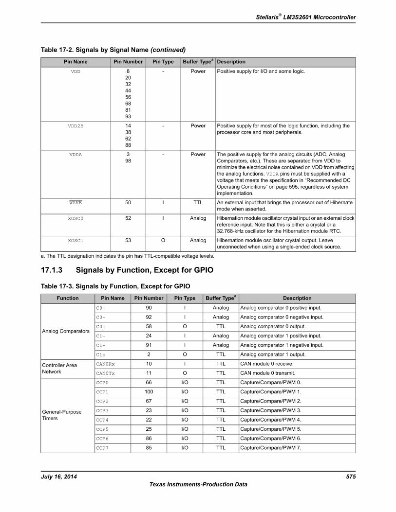
Table 17-2. Signals by Signal Name (continued)
DescriptionBuffer TypeaPin TypePin NumberPin Name
Positive supply for I/O and some logic.Power-820324456688193
VDD
Positive supply for most of the logic function, including theprocessor core and most peripherals.
Power-14386288
VDD25
The positive supply for the analog circuits (ADC, AnalogComparators, etc.). These are separated from VDD tominimize the electrical noise contained on VDD from affectingthe analog functions. VDDA pins must be supplied with avoltage that meets the specification in “Recommended DCOperating Conditions” on page 595, regardless of systemimplementation.
Power-398
VDDA
An external input that brings the processor out of Hibernatemode when asserted.
TTLI50WAKE
Hibernation module oscillator crystal input or an external clockreference input. Note that this is either a crystal or a32.768-kHz oscillator for the Hibernation module RTC.
AnalogI52XOSC0
Hibernation module oscillator crystal output. Leaveunconnected when using a single-ended clock source.
AnalogO53XOSC1
a. The TTL designation indicates the pin has TTL-compatible voltage levels.
17.1.3 Signals by Function, Except for GPIO
Table 17-3. Signals by Function, Except for GPIO
DescriptionBuffer TypeaPin TypePin NumberPin NameFunction
Analog comparator 0 positive input.AnalogI90C0+
Analog Comparators
Analog comparator 0 negative input.AnalogI92C0-
Analog comparator 0 output.TTLO58C0o
Analog comparator 1 positive input.AnalogI24C1+
Analog comparator 1 negative input.AnalogI91C1-
Analog comparator 1 output.TTLO2C1o
CAN module 0 receive.TTLI10CAN0RxController AreaNetwork CAN module 0 transmit.TTLO11CAN0Tx
Capture/Compare/PWM 0.TTLI/O66CCP0
General-PurposeTimers
Capture/Compare/PWM 1.TTLI/O100CCP1
Capture/Compare/PWM 2.TTLI/O67CCP2
Capture/Compare/PWM 3.TTLI/O23CCP3
Capture/Compare/PWM 4.TTLI/O22CCP4
Capture/Compare/PWM 5.TTLI/O25CCP5
Capture/Compare/PWM 6.TTLI/O86CCP6
Capture/Compare/PWM 7.TTLI/O85CCP7
575July 16, 2014Texas Instruments-Production Data
Stellaris® LM3S2601 Microcontroller
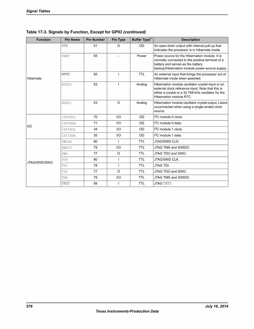
Table 17-3. Signals by Function, Except for GPIO (continued)
DescriptionBuffer TypeaPin TypePin NumberPin NameFunction
An open-drain output with internal pull-up thatindicates the processor is in Hibernate mode.
ODO51HIB
Hibernate
Power source for the Hibernation module. It isnormally connected to the positive terminal of abattery and serves as the batterybackup/Hibernation module power-source supply.
Power-55VBAT
An external input that brings the processor out ofHibernate mode when asserted.
TTLI50WAKE
Hibernation module oscillator crystal input or anexternal clock reference input. Note that this iseither a crystal or a 32.768-kHz oscillator for theHibernation module RTC.
AnalogI52XOSC0
Hibernation module oscillator crystal output. Leaveunconnected when using a single-ended clocksource.
AnalogO53XOSC1
I2C module 0 clock.ODI/O70I2C0SCL
I2CI2C module 0 data.ODI/O71I2C0SDA
I2C module 1 clock.ODI/O34I2C1SCL
I2C module 1 data.ODI/O35I2C1SDA
JTAG/SWD CLK.TTLI80SWCLK
JTAG/SWD/SWO
JTAG TMS and SWDIO.TTLI/O79SWDIO
JTAG TDO and SWO.TTLO77SWO
JTAG/SWD CLK.TTLI80TCK
JTAG TDI.TTLI78TDI
JTAG TDO and SWO.TTLO77TDO
JTAG TMS and SWDIO.TTLI/O79TMS
JTAG TRST.TTLI89TRST
July 16, 2014576Texas Instruments-Production Data
Signal Tables
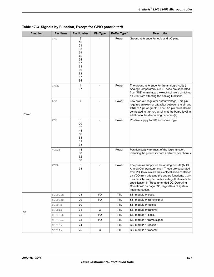
Table 17-3. Signals by Function, Except for GPIO (continued)
DescriptionBuffer TypeaPin TypePin NumberPin NameFunction
Ground reference for logic and I/O pins.Power-9152133394554576369828794
GND
Power
The ground reference for the analog circuits (Analog Comparators, etc.). These are separatedfromGND tominimize the electrical noise containedon VDD from affecting the analog functions.
Power-497
GNDA
Low drop-out regulator output voltage. This pinrequires an external capacitor between the pin andGND of 1 µF or greater. The LDO pin must also beconnected to the VDD25 pins at the board level inaddition to the decoupling capacitor(s).
Power-7LDO
Positive supply for I/O and some logic.Power-820324456688193
VDD
Positive supply for most of the logic function,including the processor core and most peripherals.
Power-14386288
VDD25
The positive supply for the analog circuits (ADC,Analog Comparators, etc.). These are separatedfrom VDD tominimize the electrical noise containedon VDD from affecting the analog functions. VDDApins must be supplied with a voltage that meets thespecification in “Recommended DC OperatingConditions” on page 595, regardless of systemimplementation.
Power-398
VDDA
SSI module 0 clock.TTLI/O28SSI0Clk
SSI
SSI module 0 frame signal.TTLI/O29SSI0Fss
SSI module 0 receive.TTLI30SSI0Rx
SSI module 0 transmit.TTLO31SSI0Tx
SSI module 1 clock.TTLI/O72SSI1Clk
SSI module 1 frame signal.TTLI/O73SSI1Fss
SSI module 1 receive.TTLI74SSI1Rx
SSI module 1 transmit.TTLO75SSI1Tx
577July 16, 2014Texas Instruments-Production Data
Stellaris® LM3S2601 Microcontroller
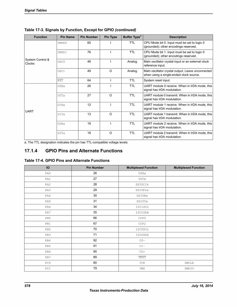
Table 17-3. Signals by Function, Except for GPIO (continued)
DescriptionBuffer TypeaPin TypePin NumberPin NameFunction
CPU Mode bit 0. Input must be set to logic 0(grounded); other encodings reserved.
TTLI65CMOD0
System Control &Clocks
CPU Mode bit 1. Input must be set to logic 0(grounded); other encodings reserved.
TTLI76CMOD1
Main oscillator crystal input or an external clockreference input.
AnalogI48OSC0
Main oscillator crystal output. Leave unconnectedwhen using a single-ended clock source.
AnalogO49OSC1
System reset input.TTLI64RST
UART module 0 receive. When in IrDA mode, thissignal has IrDA modulation.
TTLI26U0Rx
UART
UART module 0 transmit. When in IrDA mode, thissignal has IrDA modulation.
TTLO27U0Tx
UART module 1 receive. When in IrDA mode, thissignal has IrDA modulation.
TTLI12U1Rx
UART module 1 transmit. When in IrDA mode, thissignal has IrDA modulation.
TTLO13U1Tx
UART module 2 receive. When in IrDA mode, thissignal has IrDA modulation.
TTLI19U2Rx
UART module 2 transmit. When in IrDA mode, thissignal has IrDA modulation.
TTLO18U2Tx
a. The TTL designation indicates the pin has TTL-compatible voltage levels.
17.1.4 GPIO Pins and Alternate Functions
Table 17-4. GPIO Pins and Alternate Functions
Multiplexed FunctionMultiplexed FunctionPin NumberIO
U0Rx26PA0
U0Tx27PA1
SSI0Clk28PA2
SSI0Fss29PA3
SSI0Rx30PA4
SSI0Tx31PA5
I2C1SCL34PA6
I2C1SDA35PA7
CCP066PB0
CCP267PB1
I2C0SCL70PB2
I2C0SDA71PB3
C0-92PB4
C1-91PB5
C0+90PB6
TRST89PB7
SWCLKTCK80PC0
SWDIOTMS79PC1
July 16, 2014578Texas Instruments-Production Data
Signal Tables
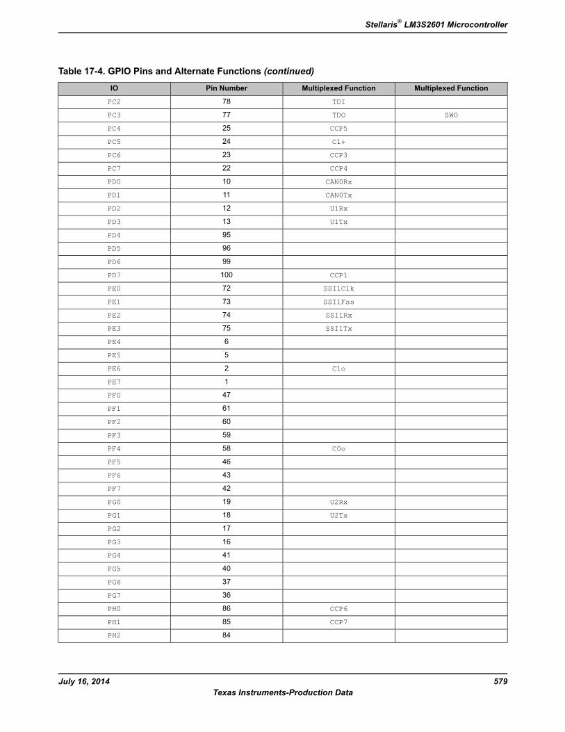
Table 17-4. GPIO Pins and Alternate Functions (continued)
Multiplexed FunctionMultiplexed FunctionPin NumberIO
TDI78PC2
SWOTDO77PC3
CCP525PC4
C1+24PC5
CCP323PC6
CCP422PC7
CAN0Rx10PD0
CAN0Tx11PD1
U1Rx12PD2
U1Tx13PD3
95PD4
96PD5
99PD6
CCP1100PD7
SSI1Clk72PE0
SSI1Fss73PE1
SSI1Rx74PE2
SSI1Tx75PE3
6PE4
5PE5
C1o2PE6
1PE7
47PF0
61PF1
60PF2
59PF3
C0o58PF4
46PF5
43PF6
42PF7
U2Rx19PG0
U2Tx18PG1
17PG2
16PG3
41PG4
40PG5
37PG6
36PG7
CCP686PH0
CCP785PH1
84PH2
579July 16, 2014Texas Instruments-Production Data
Stellaris® LM3S2601 Microcontroller
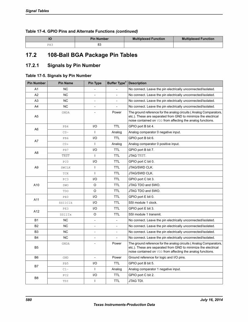
Table 17-4. GPIO Pins and Alternate Functions (continued)
Multiplexed FunctionMultiplexed FunctionPin NumberIO
83PH3
17.2 108-Ball BGA Package Pin Tables
17.2.1 Signals by Pin Number
Table 17-5. Signals by Pin Number
DescriptionBuffer TypeaPin TypePin NamePin Number
No connect. Leave the pin electrically unconnected/isolated.--NCA1
No connect. Leave the pin electrically unconnected/isolated.--NCA2
No connect. Leave the pin electrically unconnected/isolated.--NCA3
No connect. Leave the pin electrically unconnected/isolated.--NCA4
The ground reference for the analog circuits ( Analog Comparators,etc.). These are separated from GND to minimize the electricalnoise contained on VDD from affecting the analog functions.
Power-GNDAA5
GPIO port B bit 4.TTLI/OPB4A6
Analog comparator 0 negative input.AnalogIC0-
GPIO port B bit 6.TTLI/OPB6A7
Analog comparator 0 positive input.AnalogIC0+
GPIO port B bit 7.TTLI/OPB7A8
JTAG TRST.TTLITRST
GPIO port C bit 0.TTLI/OPC0
A9 JTAG/SWD CLK.TTLISWCLK
JTAG/SWD CLK.TTLITCK
GPIO port C bit 3.TTLI/OPC3
A10 JTAG TDO and SWO.TTLOSWO
JTAG TDO and SWO.TTLOTDO
GPIO port E bit 0.TTLI/OPE0A11
SSI module 1 clock.TTLI/OSSI1Clk
GPIO port E bit 3.TTLI/OPE3A12
SSI module 1 transmit.TTLOSSI1Tx
No connect. Leave the pin electrically unconnected/isolated.--NCB1
No connect. Leave the pin electrically unconnected/isolated.--NCB2
No connect. Leave the pin electrically unconnected/isolated.--NCB3
No connect. Leave the pin electrically unconnected/isolated.--NCB4
The ground reference for the analog circuits ( Analog Comparators,etc.). These are separated from GND to minimize the electricalnoise contained on VDD from affecting the analog functions.
Power-GNDAB5
Ground reference for logic and I/O pins.Power-GNDB6
GPIO port B bit 5.TTLI/OPB5B7
Analog comparator 1 negative input.AnalogIC1-
GPIO port C bit 2.TTLI/OPC2B8
JTAG TDI.TTLITDI
July 16, 2014580Texas Instruments-Production Data
Signal Tables
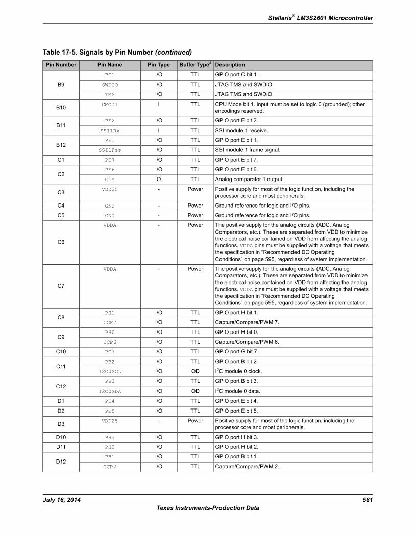
Table 17-5. Signals by Pin Number (continued)
DescriptionBuffer TypeaPin TypePin NamePin Number
GPIO port C bit 1.TTLI/OPC1
B9 JTAG TMS and SWDIO.TTLI/OSWDIO
JTAG TMS and SWDIO.TTLI/OTMS
CPU Mode bit 1. Input must be set to logic 0 (grounded); otherencodings reserved.
TTLICMOD1B10
GPIO port E bit 2.TTLI/OPE2B11
SSI module 1 receive.TTLISSI1Rx
GPIO port E bit 1.TTLI/OPE1B12
SSI module 1 frame signal.TTLI/OSSI1Fss
GPIO port E bit 7.TTLI/OPE7C1
GPIO port E bit 6.TTLI/OPE6C2
Analog comparator 1 output.TTLOC1o
Positive supply for most of the logic function, including theprocessor core and most peripherals.
Power-VDD25C3
Ground reference for logic and I/O pins.Power-GNDC4
Ground reference for logic and I/O pins.Power-GNDC5
The positive supply for the analog circuits (ADC, AnalogComparators, etc.). These are separated from VDD to minimizethe electrical noise contained on VDD from affecting the analogfunctions. VDDA pins must be supplied with a voltage that meetsthe specification in “Recommended DC OperatingConditions” on page 595, regardless of system implementation.
Power-VDDA
C6
The positive supply for the analog circuits (ADC, AnalogComparators, etc.). These are separated from VDD to minimizethe electrical noise contained on VDD from affecting the analogfunctions. VDDA pins must be supplied with a voltage that meetsthe specification in “Recommended DC OperatingConditions” on page 595, regardless of system implementation.
Power-VDDA
C7
GPIO port H bit 1.TTLI/OPH1C8
Capture/Compare/PWM 7.TTLI/OCCP7
GPIO port H bit 0.TTLI/OPH0C9
Capture/Compare/PWM 6.TTLI/OCCP6
GPIO port G bit 7.TTLI/OPG7C10
GPIO port B bit 2.TTLI/OPB2C11
I2C module 0 clock.ODI/OI2C0SCL
GPIO port B bit 3.TTLI/OPB3C12
I2C module 0 data.ODI/OI2C0SDA
GPIO port E bit 4.TTLI/OPE4D1
GPIO port E bit 5.TTLI/OPE5D2
Positive supply for most of the logic function, including theprocessor core and most peripherals.
Power-VDD25D3
GPIO port H bit 3.TTLI/OPH3D10
GPIO port H bit 2.TTLI/OPH2D11
GPIO port B bit 1.TTLI/OPB1D12
Capture/Compare/PWM 2.TTLI/OCCP2
581July 16, 2014Texas Instruments-Production Data
Stellaris® LM3S2601 Microcontroller
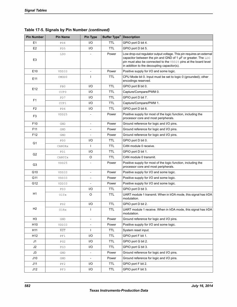
Table 17-5. Signals by Pin Number (continued)
DescriptionBuffer TypeaPin TypePin NamePin Number
GPIO port D bit 4.TTLI/OPD4E1
GPIO port D bit 5.TTLI/OPD5E2
Low drop-out regulator output voltage. This pin requires an externalcapacitor between the pin and GND of 1 µF or greater. The LDOpin must also be connected to the VDD25 pins at the board levelin addition to the decoupling capacitor(s).
Power-LDO
E3
Positive supply for I/O and some logic.Power-VDD33E10
CPU Mode bit 0. Input must be set to logic 0 (grounded); otherencodings reserved.
TTLICMOD0E11
GPIO port B bit 0.TTLI/OPB0E12
Capture/Compare/PWM 0.TTLI/OCCP0
GPIO port D bit 7.TTLI/OPD7F1
Capture/Compare/PWM 1.TTLI/OCCP1
GPIO port D bit 6.TTLI/OPD6F2
Positive supply for most of the logic function, including theprocessor core and most peripherals.
Power-VDD25F3
Ground reference for logic and I/O pins.Power-GNDF10
Ground reference for logic and I/O pins.Power-GNDF11
Ground reference for logic and I/O pins.Power-GNDF12
GPIO port D bit 0.TTLI/OPD0G1
CAN module 0 receive.TTLICAN0Rx
GPIO port D bit 1.TTLI/OPD1G2
CAN module 0 transmit.TTLOCAN0Tx
Positive supply for most of the logic function, including theprocessor core and most peripherals.
Power-VDD25G3
Positive supply for I/O and some logic.Power-VDD33G10
Positive supply for I/O and some logic.Power-VDD33G11
Positive supply for I/O and some logic.Power-VDD33G12
GPIO port D bit 3.TTLI/OPD3
H1 UARTmodule 1 transmit. When in IrDA mode, this signal has IrDAmodulation.
TTLOU1Tx
GPIO port D bit 2.TTLI/OPD2
H2 UART module 1 receive. When in IrDA mode, this signal has IrDAmodulation.
TTLIU1Rx
Ground reference for logic and I/O pins.Power-GNDH3
Positive supply for I/O and some logic.Power-VDD33H10
System reset input.TTLIRSTH11
GPIO port F bit 1.TTLI/OPF1H12
GPIO port G bit 2.TTLI/OPG2J1
GPIO port G bit 3.TTLI/OPG3J2
Ground reference for logic and I/O pins.Power-GNDJ3
Ground reference for logic and I/O pins.Power-GNDJ10
GPIO port F bit 2.TTLI/OPF2J11
GPIO port F bit 3.TTLI/OPF3J12
July 16, 2014582Texas Instruments-Production Data
Signal Tables
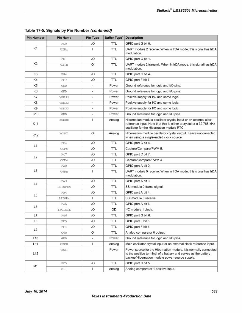
Table 17-5. Signals by Pin Number (continued)
DescriptionBuffer TypeaPin TypePin NamePin Number
GPIO port G bit 0.TTLI/OPG0
K1 UART module 2 receive. When in IrDA mode, this signal has IrDAmodulation.
TTLIU2Rx
GPIO port G bit 1.TTLI/OPG1
K2 UARTmodule 2 transmit. When in IrDA mode, this signal has IrDAmodulation.
TTLOU2Tx
GPIO port G bit 4.TTLI/OPG4K3
GPIO port F bit 7.TTLI/OPF7K4
Ground reference for logic and I/O pins.Power-GNDK5
Ground reference for logic and I/O pins.Power-GNDK6
Positive supply for I/O and some logic.Power-VDD33K7
Positive supply for I/O and some logic.Power-VDD33K8
Positive supply for I/O and some logic.Power-VDD33K9
Ground reference for logic and I/O pins.Power-GNDK10
Hibernation module oscillator crystal input or an external clockreference input. Note that this is either a crystal or a 32.768-kHzoscillator for the Hibernation module RTC.
AnalogIXOSC0K11
Hibernation module oscillator crystal output. Leave unconnectedwhen using a single-ended clock source.
AnalogOXOSC1K12
GPIO port C bit 4.TTLI/OPC4L1
Capture/Compare/PWM 5.TTLI/OCCP5
GPIO port C bit 7.TTLI/OPC7L2
Capture/Compare/PWM 4.TTLI/OCCP4
GPIO port A bit 0.TTLI/OPA0
L3 UART module 0 receive. When in IrDA mode, this signal has IrDAmodulation.
TTLIU0Rx
GPIO port A bit 3.TTLI/OPA3L4
SSI module 0 frame signal.TTLI/OSSI0Fss
GPIO port A bit 4.TTLI/OPA4L5
SSI module 0 receive.TTLISSI0Rx
GPIO port A bit 6.TTLI/OPA6L6
I2C module 1 clock.ODI/OI2C1SCL
GPIO port G bit 6.TTLI/OPG6L7
GPIO port F bit 5.TTLI/OPF5L8
GPIO port F bit 4.TTLI/OPF4L9
Analog comparator 0 output.TTLOC0o
Ground reference for logic and I/O pins.Power-GNDL10
Main oscillator crystal input or an external clock reference input.AnalogIOSC0L11
Power source for the Hibernation module. It is normally connectedto the positive terminal of a battery and serves as the batterybackup/Hibernation module power-source supply.
Power-VBATL12
GPIO port C bit 5.TTLI/OPC5M1
Analog comparator 1 positive input.AnalogIC1+
583July 16, 2014Texas Instruments-Production Data
Stellaris® LM3S2601 Microcontroller
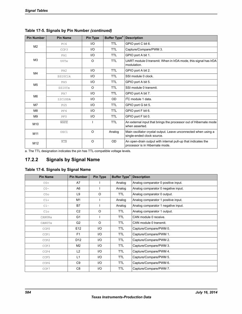
Table 17-5. Signals by Pin Number (continued)
DescriptionBuffer TypeaPin TypePin NamePin Number
GPIO port C bit 6.TTLI/OPC6M2
Capture/Compare/PWM 3.TTLI/OCCP3
GPIO port A bit 1.TTLI/OPA1
M3 UARTmodule 0 transmit. When in IrDA mode, this signal has IrDAmodulation.
TTLOU0Tx
GPIO port A bit 2.TTLI/OPA2M4
SSI module 0 clock.TTLI/OSSI0Clk
GPIO port A bit 5.TTLI/OPA5M5
SSI module 0 transmit.TTLOSSI0Tx
GPIO port A bit 7.TTLI/OPA7M6
I2C module 1 data.ODI/OI2C1SDA
GPIO port G bit 5.TTLI/OPG5M7
GPIO port F bit 6.TTLI/OPF6M8
GPIO port F bit 0.TTLI/OPF0M9
An external input that brings the processor out of Hibernate modewhen asserted.
TTLIWAKEM10
Main oscillator crystal output. Leave unconnected when using asingle-ended clock source.
AnalogOOSC1M11
An open-drain output with internal pull-up that indicates theprocessor is in Hibernate mode.
ODOHIBM12
a. The TTL designation indicates the pin has TTL-compatible voltage levels.
17.2.2 Signals by Signal Name
Table 17-6. Signals by Signal Name
DescriptionBuffer TypeaPin TypePin NumberPin Name
Analog comparator 0 positive input.AnalogIA7C0+
Analog comparator 0 negative input.AnalogIA6C0-
Analog comparator 0 output.TTLOL9C0o
Analog comparator 1 positive input.AnalogIM1C1+
Analog comparator 1 negative input.AnalogIB7C1-
Analog comparator 1 output.TTLOC2C1o
CAN module 0 receive.TTLIG1CAN0Rx
CAN module 0 transmit.TTLOG2CAN0Tx
Capture/Compare/PWM 0.TTLI/OE12CCP0
Capture/Compare/PWM 1.TTLI/OF1CCP1
Capture/Compare/PWM 2.TTLI/OD12CCP2
Capture/Compare/PWM 3.TTLI/OM2CCP3
Capture/Compare/PWM 4.TTLI/OL2CCP4
Capture/Compare/PWM 5.TTLI/OL1CCP5
Capture/Compare/PWM 6.TTLI/OC9CCP6
Capture/Compare/PWM 7.TTLI/OC8CCP7
July 16, 2014584Texas Instruments-Production Data
Signal Tables
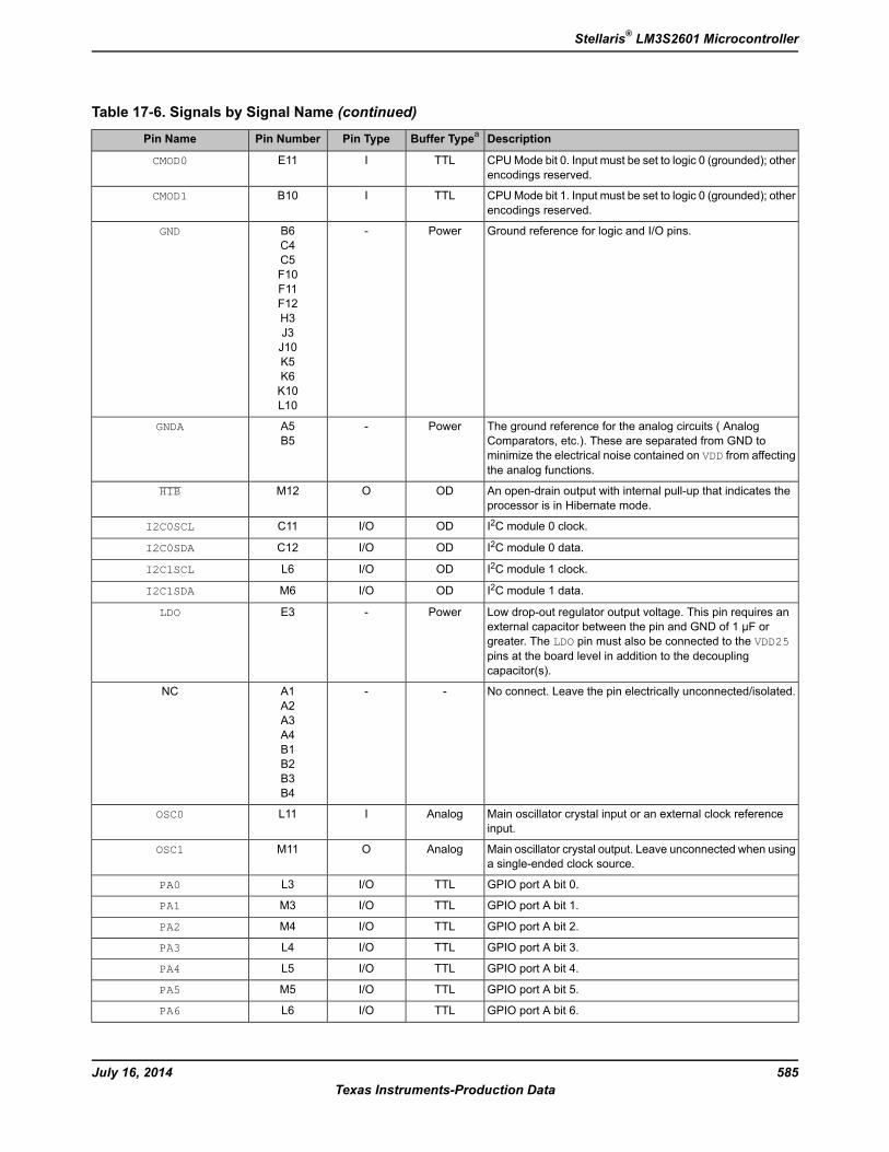
Table 17-6. Signals by Signal Name (continued)
DescriptionBuffer TypeaPin TypePin NumberPin Name
CPUMode bit 0. Input must be set to logic 0 (grounded); otherencodings reserved.
TTLIE11CMOD0
CPUMode bit 1. Input must be set to logic 0 (grounded); otherencodings reserved.
TTLIB10CMOD1
Ground reference for logic and I/O pins.Power-B6C4C5F10F11F12H3J3J10K5K6K10L10
GND
The ground reference for the analog circuits ( AnalogComparators, etc.). These are separated from GND tominimize the electrical noise contained on VDD from affectingthe analog functions.
Power-A5B5
GNDA
An open-drain output with internal pull-up that indicates theprocessor is in Hibernate mode.
ODOM12HIB
I2C module 0 clock.ODI/OC11I2C0SCL
I2C module 0 data.ODI/OC12I2C0SDA
I2C module 1 clock.ODI/OL6I2C1SCL
I2C module 1 data.ODI/OM6I2C1SDA
Low drop-out regulator output voltage. This pin requires anexternal capacitor between the pin and GND of 1 µF orgreater. The LDO pin must also be connected to the VDD25pins at the board level in addition to the decouplingcapacitor(s).
Power-E3LDO
No connect. Leave the pin electrically unconnected/isolated.--A1A2A3A4B1B2B3B4
NC
Main oscillator crystal input or an external clock referenceinput.
AnalogIL11OSC0
Main oscillator crystal output. Leave unconnected when usinga single-ended clock source.
AnalogOM11OSC1
GPIO port A bit 0.TTLI/OL3PA0
GPIO port A bit 1.TTLI/OM3PA1
GPIO port A bit 2.TTLI/OM4PA2
GPIO port A bit 3.TTLI/OL4PA3
GPIO port A bit 4.TTLI/OL5PA4
GPIO port A bit 5.TTLI/OM5PA5
GPIO port A bit 6.TTLI/OL6PA6
585July 16, 2014Texas Instruments-Production Data
Stellaris® LM3S2601 Microcontroller
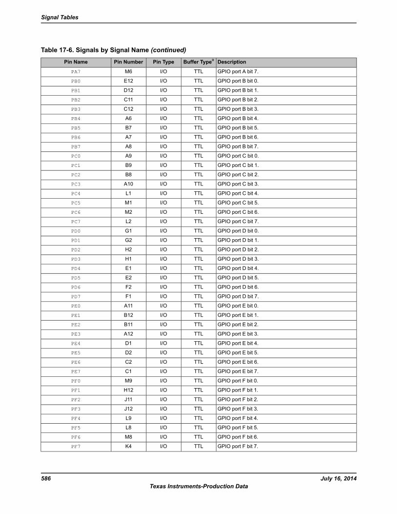
Table 17-6. Signals by Signal Name (continued)
DescriptionBuffer TypeaPin TypePin NumberPin Name
GPIO port A bit 7.TTLI/OM6PA7
GPIO port B bit 0.TTLI/OE12PB0
GPIO port B bit 1.TTLI/OD12PB1
GPIO port B bit 2.TTLI/OC11PB2
GPIO port B bit 3.TTLI/OC12PB3
GPIO port B bit 4.TTLI/OA6PB4
GPIO port B bit 5.TTLI/OB7PB5
GPIO port B bit 6.TTLI/OA7PB6
GPIO port B bit 7.TTLI/OA8PB7
GPIO port C bit 0.TTLI/OA9PC0
GPIO port C bit 1.TTLI/OB9PC1
GPIO port C bit 2.TTLI/OB8PC2
GPIO port C bit 3.TTLI/OA10PC3
GPIO port C bit 4.TTLI/OL1PC4
GPIO port C bit 5.TTLI/OM1PC5
GPIO port C bit 6.TTLI/OM2PC6
GPIO port C bit 7.TTLI/OL2PC7
GPIO port D bit 0.TTLI/OG1PD0
GPIO port D bit 1.TTLI/OG2PD1
GPIO port D bit 2.TTLI/OH2PD2
GPIO port D bit 3.TTLI/OH1PD3
GPIO port D bit 4.TTLI/OE1PD4
GPIO port D bit 5.TTLI/OE2PD5
GPIO port D bit 6.TTLI/OF2PD6
GPIO port D bit 7.TTLI/OF1PD7
GPIO port E bit 0.TTLI/OA11PE0
GPIO port E bit 1.TTLI/OB12PE1
GPIO port E bit 2.TTLI/OB11PE2
GPIO port E bit 3.TTLI/OA12PE3
GPIO port E bit 4.TTLI/OD1PE4
GPIO port E bit 5.TTLI/OD2PE5
GPIO port E bit 6.TTLI/OC2PE6
GPIO port E bit 7.TTLI/OC1PE7
GPIO port F bit 0.TTLI/OM9PF0
GPIO port F bit 1.TTLI/OH12PF1
GPIO port F bit 2.TTLI/OJ11PF2
GPIO port F bit 3.TTLI/OJ12PF3
GPIO port F bit 4.TTLI/OL9PF4
GPIO port F bit 5.TTLI/OL8PF5
GPIO port F bit 6.TTLI/OM8PF6
GPIO port F bit 7.TTLI/OK4PF7
July 16, 2014586Texas Instruments-Production Data
Signal Tables
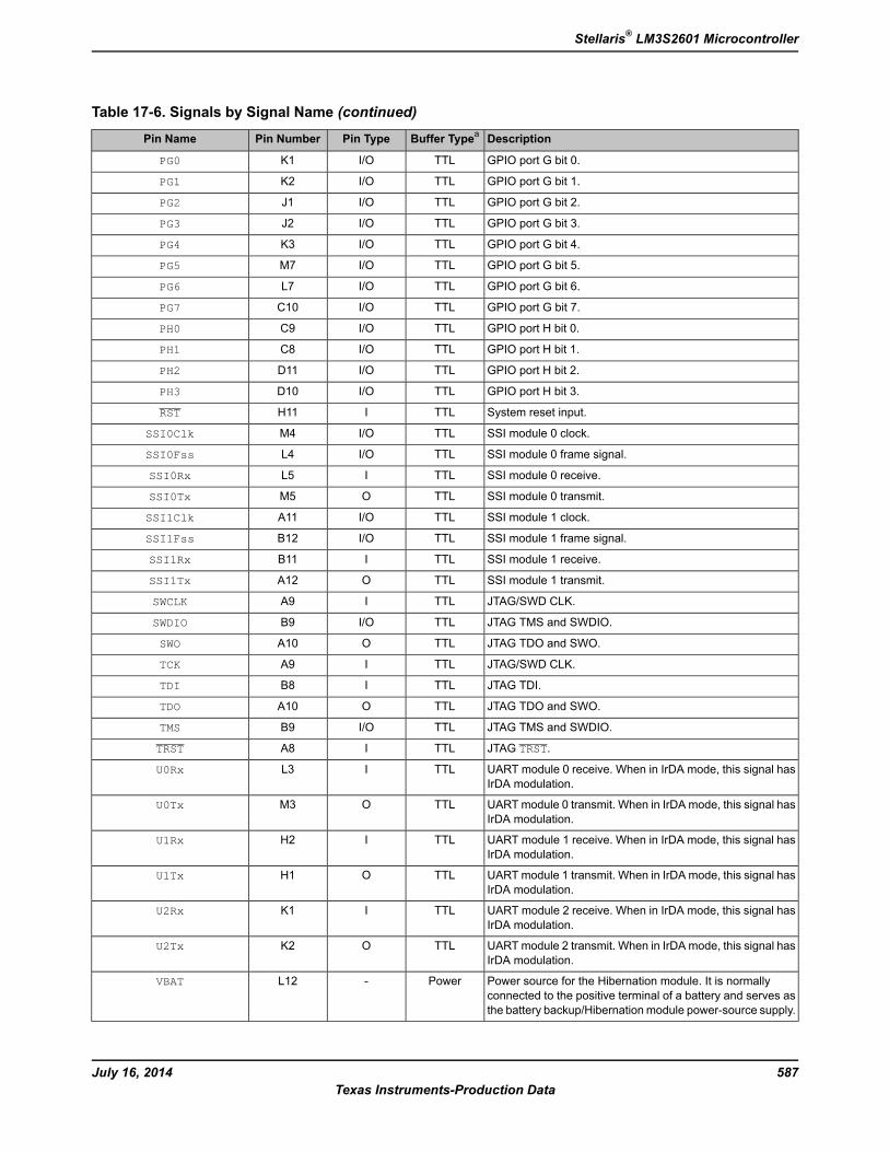
Table 17-6. Signals by Signal Name (continued)
DescriptionBuffer TypeaPin TypePin NumberPin Name
GPIO port G bit 0.TTLI/OK1PG0
GPIO port G bit 1.TTLI/OK2PG1
GPIO port G bit 2.TTLI/OJ1PG2
GPIO port G bit 3.TTLI/OJ2PG3
GPIO port G bit 4.TTLI/OK3PG4
GPIO port G bit 5.TTLI/OM7PG5
GPIO port G bit 6.TTLI/OL7PG6
GPIO port G bit 7.TTLI/OC10PG7
GPIO port H bit 0.TTLI/OC9PH0
GPIO port H bit 1.TTLI/OC8PH1
GPIO port H bit 2.TTLI/OD11PH2
GPIO port H bit 3.TTLI/OD10PH3
System reset input.TTLIH11RST
SSI module 0 clock.TTLI/OM4SSI0Clk
SSI module 0 frame signal.TTLI/OL4SSI0Fss
SSI module 0 receive.TTLIL5SSI0Rx
SSI module 0 transmit.TTLOM5SSI0Tx
SSI module 1 clock.TTLI/OA11SSI1Clk
SSI module 1 frame signal.TTLI/OB12SSI1Fss
SSI module 1 receive.TTLIB11SSI1Rx
SSI module 1 transmit.TTLOA12SSI1Tx
JTAG/SWD CLK.TTLIA9SWCLK
JTAG TMS and SWDIO.TTLI/OB9SWDIO
JTAG TDO and SWO.TTLOA10SWO
JTAG/SWD CLK.TTLIA9TCK
JTAG TDI.TTLIB8TDI
JTAG TDO and SWO.TTLOA10TDO
JTAG TMS and SWDIO.TTLI/OB9TMS
JTAG TRST.TTLIA8TRST
UART module 0 receive. When in IrDA mode, this signal hasIrDA modulation.
TTLIL3U0Rx
UARTmodule 0 transmit. When in IrDA mode, this signal hasIrDA modulation.
TTLOM3U0Tx
UART module 1 receive. When in IrDA mode, this signal hasIrDA modulation.
TTLIH2U1Rx
UARTmodule 1 transmit. When in IrDA mode, this signal hasIrDA modulation.
TTLOH1U1Tx
UART module 2 receive. When in IrDA mode, this signal hasIrDA modulation.
TTLIK1U2Rx
UARTmodule 2 transmit. When in IrDA mode, this signal hasIrDA modulation.
TTLOK2U2Tx
Power source for the Hibernation module. It is normallyconnected to the positive terminal of a battery and serves asthe battery backup/Hibernation module power-source supply.
Power-L12VBAT
587July 16, 2014Texas Instruments-Production Data
Stellaris® LM3S2601 Microcontroller
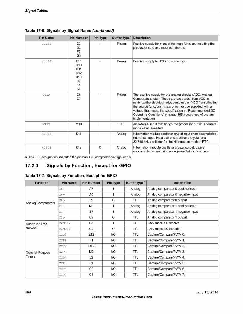
Table 17-6. Signals by Signal Name (continued)
DescriptionBuffer TypeaPin TypePin NumberPin Name
Positive supply for most of the logic function, including theprocessor core and most peripherals.
Power-C3D3F3G3
VDD25
Positive supply for I/O and some logic.Power-E10G10G11G12H10K7K8K9
VDD33
The positive supply for the analog circuits (ADC, AnalogComparators, etc.). These are separated from VDD tominimize the electrical noise contained on VDD from affectingthe analog functions. VDDA pins must be supplied with avoltage that meets the specification in “Recommended DCOperating Conditions” on page 595, regardless of systemimplementation.
Power-C6C7
VDDA
An external input that brings the processor out of Hibernatemode when asserted.
TTLIM10WAKE
Hibernation module oscillator crystal input or an external clockreference input. Note that this is either a crystal or a32.768-kHz oscillator for the Hibernation module RTC.
AnalogIK11XOSC0
Hibernation module oscillator crystal output. Leaveunconnected when using a single-ended clock source.
AnalogOK12XOSC1
a. The TTL designation indicates the pin has TTL-compatible voltage levels.
17.2.3 Signals by Function, Except for GPIO
Table 17-7. Signals by Function, Except for GPIO
DescriptionBuffer TypeaPin TypePin NumberPin NameFunction
Analog comparator 0 positive input.AnalogIA7C0+
Analog Comparators
Analog comparator 0 negative input.AnalogIA6C0-
Analog comparator 0 output.TTLOL9C0o
Analog comparator 1 positive input.AnalogIM1C1+
Analog comparator 1 negative input.AnalogIB7C1-
Analog comparator 1 output.TTLOC2C1o
CAN module 0 receive.TTLIG1CAN0RxController AreaNetwork CAN module 0 transmit.TTLOG2CAN0Tx
Capture/Compare/PWM 0.TTLI/OE12CCP0
General-PurposeTimers
Capture/Compare/PWM 1.TTLI/OF1CCP1
Capture/Compare/PWM 2.TTLI/OD12CCP2
Capture/Compare/PWM 3.TTLI/OM2CCP3
Capture/Compare/PWM 4.TTLI/OL2CCP4
Capture/Compare/PWM 5.TTLI/OL1CCP5
Capture/Compare/PWM 6.TTLI/OC9CCP6
Capture/Compare/PWM 7.TTLI/OC8CCP7
July 16, 2014588Texas Instruments-Production Data
Signal Tables
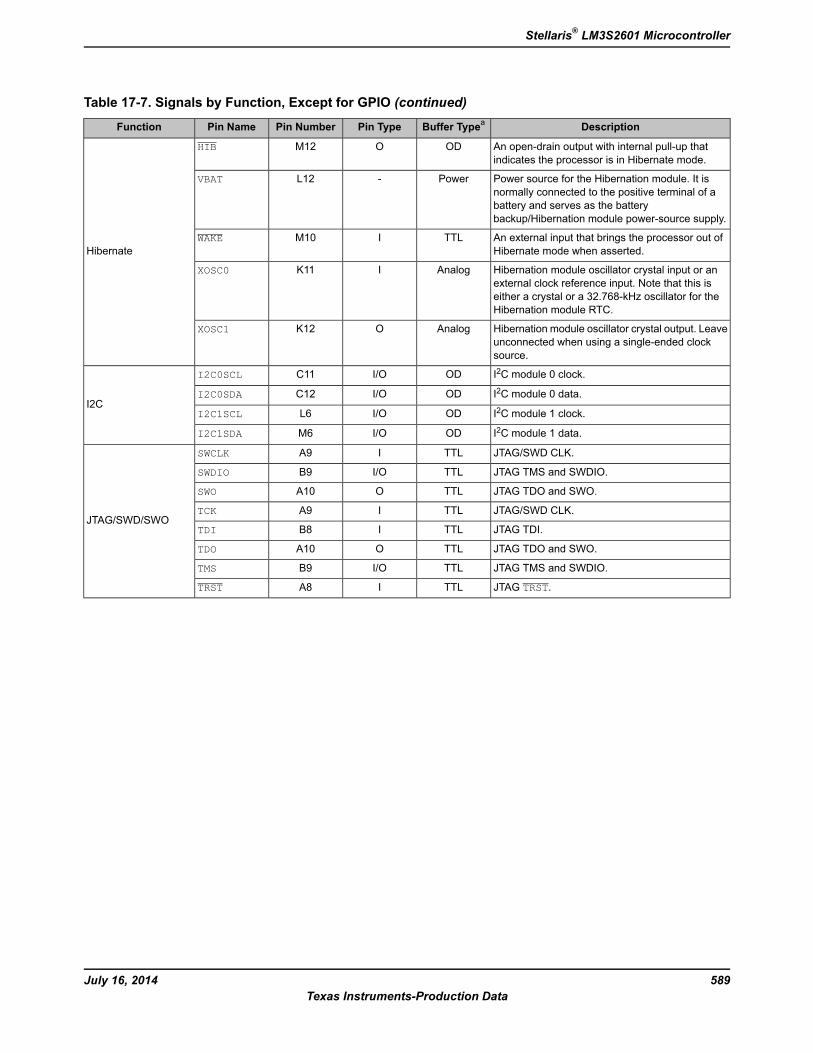
Table 17-7. Signals by Function, Except for GPIO (continued)
DescriptionBuffer TypeaPin TypePin NumberPin NameFunction
An open-drain output with internal pull-up thatindicates the processor is in Hibernate mode.
ODOM12HIB
Hibernate
Power source for the Hibernation module. It isnormally connected to the positive terminal of abattery and serves as the batterybackup/Hibernation module power-source supply.
Power-L12VBAT
An external input that brings the processor out ofHibernate mode when asserted.
TTLIM10WAKE
Hibernation module oscillator crystal input or anexternal clock reference input. Note that this iseither a crystal or a 32.768-kHz oscillator for theHibernation module RTC.
AnalogIK11XOSC0
Hibernation module oscillator crystal output. Leaveunconnected when using a single-ended clocksource.
AnalogOK12XOSC1
I2C module 0 clock.ODI/OC11I2C0SCL
I2CI2C module 0 data.ODI/OC12I2C0SDA
I2C module 1 clock.ODI/OL6I2C1SCL
I2C module 1 data.ODI/OM6I2C1SDA
JTAG/SWD CLK.TTLIA9SWCLK
JTAG/SWD/SWO
JTAG TMS and SWDIO.TTLI/OB9SWDIO
JTAG TDO and SWO.TTLOA10SWO
JTAG/SWD CLK.TTLIA9TCK
JTAG TDI.TTLIB8TDI
JTAG TDO and SWO.TTLOA10TDO
JTAG TMS and SWDIO.TTLI/OB9TMS
JTAG TRST.TTLIA8TRST
589July 16, 2014Texas Instruments-Production Data
Stellaris® LM3S2601 Microcontroller
Table 17-7. Signals by Function, Except for GPIO (continued)
DescriptionBuffer TypeaPin TypePin NumberPin NameFunction
Ground reference for logic and I/O pins.Power-B6C4C5F10F11F12H3J3J10K5K6K10L10
GND
Power
The ground reference for the analog circuits (Analog Comparators, etc.). These are separatedfromGND tominimize the electrical noise containedon VDD from affecting the analog functions.
Power-A5B5
GNDA
Low drop-out regulator output voltage. This pinrequires an external capacitor between the pin andGND of 1 µF or greater. The LDO pin must also beconnected to the VDD25 pins at the board level inaddition to the decoupling capacitor(s).
Power-E3LDO
Positive supply for most of the logic function,including the processor core and most peripherals.
Power-C3D3F3G3
VDD25
Positive supply for I/O and some logic.Power-E10G10G11G12H10K7K8K9
VDD33
The positive supply for the analog circuits (ADC,Analog Comparators, etc.). These are separatedfrom VDD tominimize the electrical noise containedon VDD from affecting the analog functions. VDDApins must be supplied with a voltage that meets thespecification in “Recommended DC OperatingConditions” on page 595, regardless of systemimplementation.
Power-C6C7
VDDA
SSI module 0 clock.TTLI/OM4SSI0Clk
SSI
SSI module 0 frame signal.TTLI/OL4SSI0Fss
SSI module 0 receive.TTLIL5SSI0Rx
SSI module 0 transmit.TTLOM5SSI0Tx
SSI module 1 clock.TTLI/OA11SSI1Clk
SSI module 1 frame signal.TTLI/OB12SSI1Fss
SSI module 1 receive.TTLIB11SSI1Rx
SSI module 1 transmit.TTLOA12SSI1Tx
July 16, 2014590Texas Instruments-Production Data
Signal Tables
Table 17-7. Signals by Function, Except for GPIO (continued)
DescriptionBuffer TypeaPin TypePin NumberPin NameFunction
CPU Mode bit 0. Input must be set to logic 0(grounded); other encodings reserved.
TTLIE11CMOD0
System Control &Clocks
CPU Mode bit 1. Input must be set to logic 0(grounded); other encodings reserved.
TTLIB10CMOD1
Main oscillator crystal input or an external clockreference input.
AnalogIL11OSC0
Main oscillator crystal output. Leave unconnectedwhen using a single-ended clock source.
AnalogOM11OSC1
System reset input.TTLIH11RST
UART module 0 receive. When in IrDA mode, thissignal has IrDA modulation.
TTLIL3U0Rx
UART
UART module 0 transmit. When in IrDA mode, thissignal has IrDA modulation.
TTLOM3U0Tx
UART module 1 receive. When in IrDA mode, thissignal has IrDA modulation.
TTLIH2U1Rx
UART module 1 transmit. When in IrDA mode, thissignal has IrDA modulation.
TTLOH1U1Tx
UART module 2 receive. When in IrDA mode, thissignal has IrDA modulation.
TTLIK1U2Rx
UART module 2 transmit. When in IrDA mode, thissignal has IrDA modulation.
TTLOK2U2Tx
a. The TTL designation indicates the pin has TTL-compatible voltage levels.
17.2.4 GPIO Pins and Alternate Functions
Table 17-8. GPIO Pins and Alternate Functions
Multiplexed FunctionMultiplexed FunctionPin NumberIO
U0RxL3PA0
U0TxM3PA1
SSI0ClkM4PA2
SSI0FssL4PA3
SSI0RxL5PA4
SSI0TxM5PA5
I2C1SCLL6PA6
I2C1SDAM6PA7
CCP0E12PB0
CCP2D12PB1
I2C0SCLC11PB2
I2C0SDAC12PB3
C0-A6PB4
C1-B7PB5
C0+A7PB6
TRSTA8PB7
SWCLKTCKA9PC0
SWDIOTMSB9PC1
591July 16, 2014Texas Instruments-Production Data
Stellaris® LM3S2601 Microcontroller
Table 17-8. GPIO Pins and Alternate Functions (continued)
Multiplexed FunctionMultiplexed FunctionPin NumberIO
TDIB8PC2
SWOTDOA10PC3
CCP5L1PC4
C1+M1PC5
CCP3M2PC6
CCP4L2PC7
CAN0RxG1PD0
CAN0TxG2PD1
U1RxH2PD2
U1TxH1PD3
E1PD4
E2PD5
F2PD6
CCP1F1PD7
SSI1ClkA11PE0
SSI1FssB12PE1
SSI1RxB11PE2
SSI1TxA12PE3
D1PE4
D2PE5
C1oC2PE6
C1PE7
M9PF0
H12PF1
J11PF2
J12PF3
C0oL9PF4
L8PF5
M8PF6
K4PF7
U2RxK1PG0
U2TxK2PG1
J1PG2
J2PG3
K3PG4
M7PG5
L7PG6
C10PG7
CCP6C9PH0
CCP7C8PH1
D11PH2
July 16, 2014592Texas Instruments-Production Data
Signal Tables
Table 17-8. GPIO Pins and Alternate Functions (continued)
Multiplexed FunctionMultiplexed FunctionPin NumberIO
D10PH3
17.3 Connections for Unused SignalsTable 17-9 on page 593 show how to handle signals for functions that are not used in a particularsystem implementation for devices that are in a 100-pin LQFP package. Two options are shown inthe table: an acceptable practice and a preferred practice for reduced power consumption andimproved EMC characteristics. If a module is not used in a system, and its inputs are grounded, itis important that the clock to the module is never enabled by setting the corresponding bit in theRCGCx register.
Table 17-9. Connections for Unused Signals (100-pin LQFP)
Preferred PracticeAcceptable PracticePin NumberSignal NameFunction
GNDNC-All unused GPIOsGPIO
NCNC51HIB
Hibernate
GNDNC55VBAT
GNDNC50WAKE
GNDNC52XOSC0
NCNC53XOSC1
NCNC-NCNo Connects
GNDNC48OSC0
System Control NCNC49OSC1
Connect through a capacitor toGND as close to pin as possible
Pull up as shown in Figure5-1 on page 167
64RST
Table 17-10 on page 593 show how to handle signals for functions that are not used in a particularsystem implementation for devices that are in a 108-pin BGA package. Two options are shown inthe table: an acceptable practice and a preferred practice for reduced power consumption andimproved EMC characteristics. If a module is not used in a system, and its inputs are grounded, itis important that the clock to the module is never enabled by setting the corresponding bit in theRCGCx register.
Table 17-10. Connections for Unused Signals, 108-pin BGA
Preferred PracticeAcceptable PracticePin NumberSignal NameFunction
GNDNC-All unused GPIOsGPIO
NCNCM12HIB
Hibernate
GNDNCL12VBAT
GNDNCM10WAKE
GNDNCK11XOSC0
NCNCK12XOSC1
NCNC-NCNo Connects
GNDNCL11OSC0
System Control NCNCM11OSC1
Connect through a capacitor toGND as close to pin as possible
Pull up as shown in Figure5-1 on page 167
H11RST
593July 16, 2014Texas Instruments-Production Data
Stellaris® LM3S2601 Microcontroller
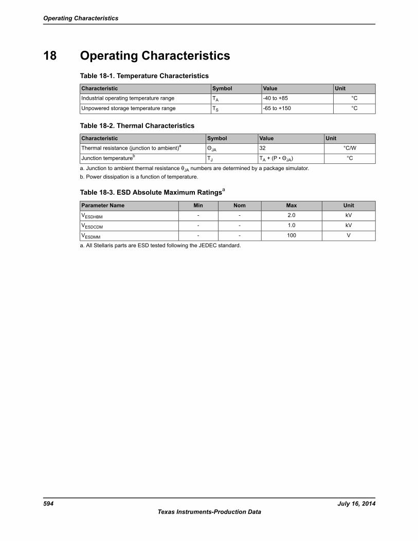
18 Operating CharacteristicsTable 18-1. Temperature Characteristics
UnitValueSymbolCharacteristic
°C-40 to +85TAIndustrial operating temperature range
°C-65 to +150TSUnpowered storage temperature range
Table 18-2. Thermal Characteristics
UnitValueSymbolCharacteristic
°C/W32ΘJAThermal resistance (junction to ambient)a
°CTA + (P • ΘJA)TJJunction temperatureb
a. Junction to ambient thermal resistance θJA numbers are determined by a package simulator.b. Power dissipation is a function of temperature.
Table 18-3. ESD Absolute Maximum Ratingsa
UnitMaxNomMinParameter Name
kV2.0--VESDHBMkV1.0--VESDCDMV100--VESDMM
a. All Stellaris parts are ESD tested following the JEDEC standard.
July 16, 2014594Texas Instruments-Production Data
Operating Characteristics
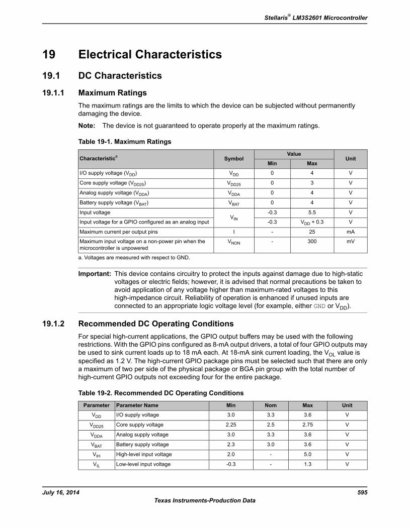
19 Electrical Characteristics19.1 DC Characteristics
19.1.1 Maximum RatingsThe maximum ratings are the limits to which the device can be subjected without permanentlydamaging the device.
Note: The device is not guaranteed to operate properly at the maximum ratings.
Table 19-1. Maximum Ratings
UnitValue
SymbolCharacteristicaMaxMin
V40VDDI/O supply voltage (VDD)
V30VDD25Core supply voltage (VDD25)
V40VDDAAnalog supply voltage (VDDA)
V40VBATBattery supply voltage (VBAT)
V5.5-0.3VIN
Input voltage
VVDD + 0.3-0.3Input voltage for a GPIO configured as an analog input
mA25-IMaximum current per output pins
mV300-VNONMaximum input voltage on a non-power pin when themicrocontroller is unpowered
a. Voltages are measured with respect to GND.
Important: This device contains circuitry to protect the inputs against damage due to high-staticvoltages or electric fields; however, it is advised that normal precautions be taken toavoid application of any voltage higher than maximum-rated voltages to thishigh-impedance circuit. Reliability of operation is enhanced if unused inputs areconnected to an appropriate logic voltage level (for example, either GND or VDD).
19.1.2 Recommended DC Operating ConditionsFor special high-current applications, the GPIO output buffers may be used with the followingrestrictions. With the GPIO pins configured as 8-mA output drivers, a total of four GPIO outputs maybe used to sink current loads up to 18 mA each. At 18-mA sink current loading, the VOL value isspecified as 1.2 V. The high-current GPIO package pins must be selected such that there are onlya maximum of two per side of the physical package or BGA pin group with the total number ofhigh-current GPIO outputs not exceeding four for the entire package.
Table 19-2. Recommended DC Operating Conditions
UnitMaxNomMinParameter NameParameter
V3.63.33.0I/O supply voltageVDDV2.752.52.25Core supply voltageVDD25V3.63.33.0Analog supply voltageVDDAV3.63.02.3Battery supply voltageVBATV5.0-2.0High-level input voltageVIHV1.3--0.3Low-level input voltageVIL
595July 16, 2014Texas Instruments-Production Data
Stellaris® LM3S2601 Microcontroller
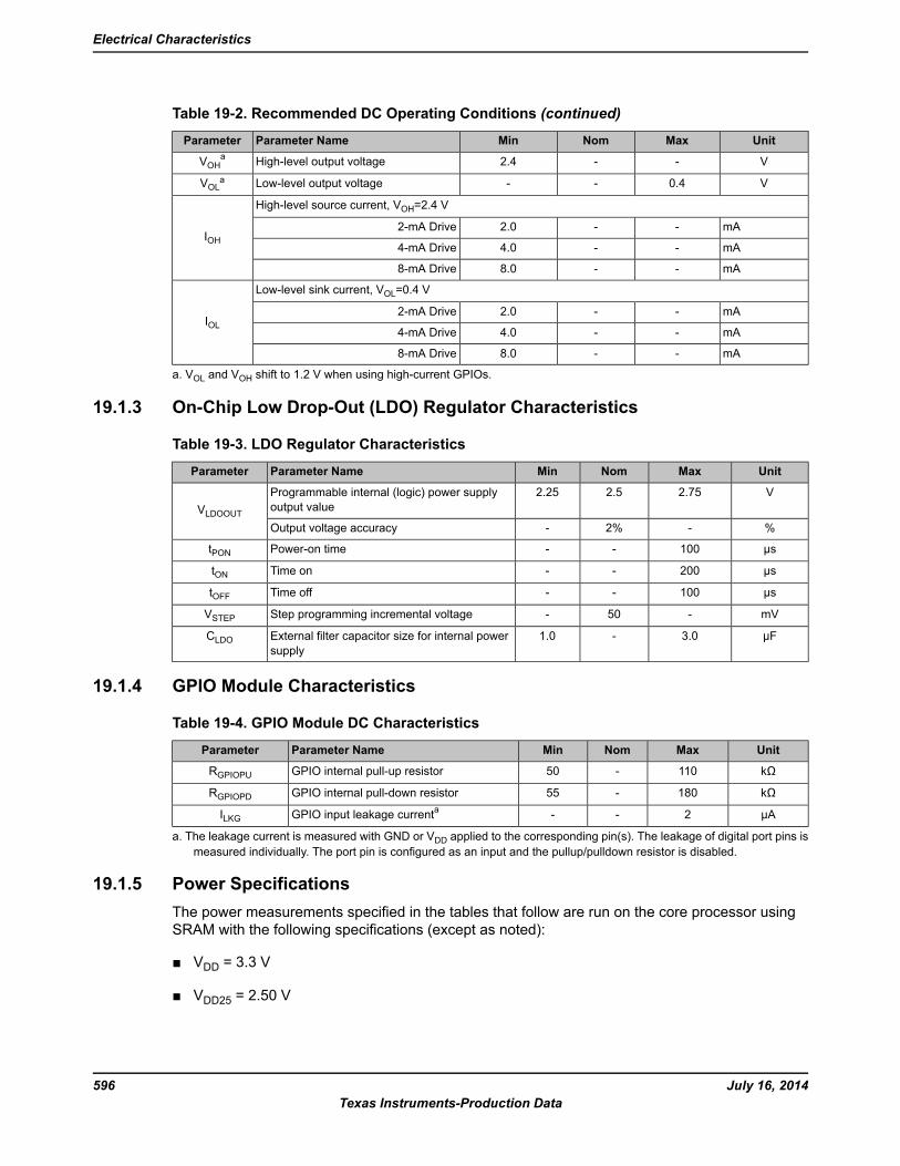
Table 19-2. Recommended DC Operating Conditions (continued)
UnitMaxNomMinParameter NameParameter
V--2.4High-level output voltageVOHa
V0.4--Low-level output voltageVOLa
High-level source current, VOH=2.4 V
IOHmA--2.02-mA Drive
mA--4.04-mA Drive
mA--8.08-mA Drive
Low-level sink current, VOL=0.4 V
IOLmA--2.02-mA Drive
mA--4.04-mA Drive
mA--8.08-mA Drive
a. VOL and VOH shift to 1.2 V when using high-current GPIOs.
19.1.3 On-Chip Low Drop-Out (LDO) Regulator Characteristics
Table 19-3. LDO Regulator Characteristics
UnitMaxNomMinParameter NameParameter
V2.752.52.25Programmable internal (logic) power supplyoutput valueVLDOOUT
%-2%-Output voltage accuracy
µs100--Power-on timetPONµs200--Time ontONµs100--Time offtOFFmV-50-Step programming incremental voltageVSTEPµF3.0-1.0External filter capacitor size for internal power
supplyCLDO
19.1.4 GPIO Module Characteristics
Table 19-4. GPIO Module DC Characteristics
UnitMaxNomMinParameter NameParameter
kΩ110-50GPIO internal pull-up resistorRGPIOPU
kΩ180-55GPIO internal pull-down resistorRGPIOPD
µA2--GPIO input leakage currentaILKGa. The leakage current is measured with GND or VDD applied to the corresponding pin(s). The leakage of digital port pins is
measured individually. The port pin is configured as an input and the pullup/pulldown resistor is disabled.
19.1.5 Power SpecificationsThe power measurements specified in the tables that follow are run on the core processor usingSRAM with the following specifications (except as noted):
VDD = 3.3 V
VDD25 = 2.50 V
July 16, 2014596Texas Instruments-Production Data
Electrical Characteristics
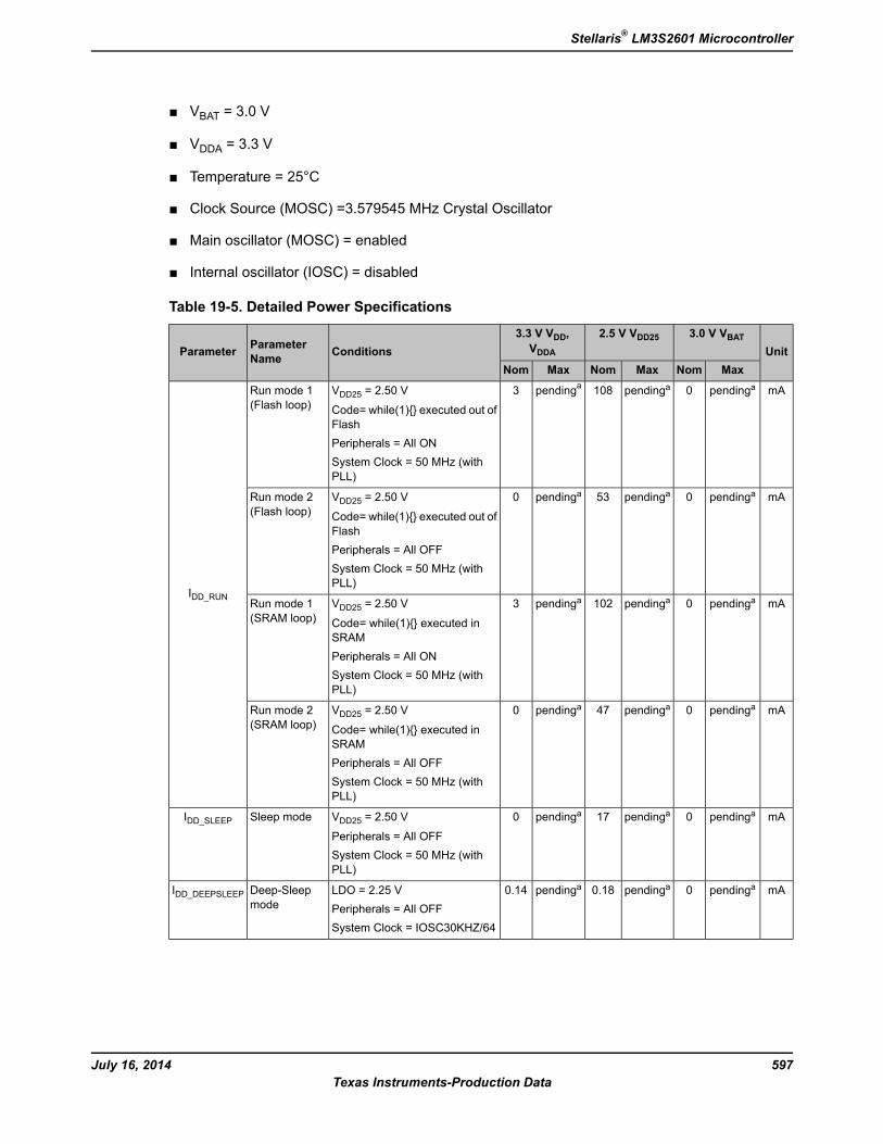
VBAT = 3.0 V
VDDA = 3.3 V
Temperature = 25°C
Clock Source (MOSC) =3.579545 MHz Crystal Oscillator
Main oscillator (MOSC) = enabled
Internal oscillator (IOSC) = disabled
Table 19-5. Detailed Power Specifications
Unit3.0 V VBAT2.5 V VDD253.3 V VDD,
VDDAConditionsParameterNameParameter
MaxNomMaxNomMaxNom
mApendinga0pendinga108pendinga3VDD25 = 2.50 V
Code= while(1) executed out ofFlashPeripherals = All ONSystem Clock = 50 MHz (withPLL)
Run mode 1(Flash loop)
IDD_RUN
mApendinga0pendinga53pendinga0VDD25 = 2.50 V
Code= while(1) executed out ofFlashPeripherals = All OFFSystem Clock = 50 MHz (withPLL)
Run mode 2(Flash loop)
mApendinga0pendinga102pendinga3VDD25 = 2.50 V
Code= while(1) executed inSRAMPeripherals = All ONSystem Clock = 50 MHz (withPLL)
Run mode 1(SRAM loop)
mApendinga0pendinga47pendinga0VDD25 = 2.50 V
Code= while(1) executed inSRAMPeripherals = All OFFSystem Clock = 50 MHz (withPLL)
Run mode 2(SRAM loop)
mApendinga0pendinga17pendinga0VDD25 = 2.50 V
Peripherals = All OFFSystem Clock = 50 MHz (withPLL)
Sleep modeIDD_SLEEP
mApendinga0pendinga0.18pendinga0.14LDO = 2.25 VPeripherals = All OFFSystem Clock = IOSC30KHZ/64
Deep-Sleepmode
IDD_DEEPSLEEP
597July 16, 2014Texas Instruments-Production Data
Stellaris® LM3S2601 Microcontroller
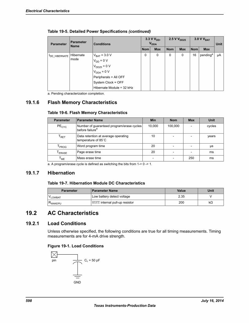
Table 19-5. Detailed Power Specifications (continued)
Unit3.0 V VBAT2.5 V VDD253.3 V VDD,
VDDAConditionsParameterNameParameter
MaxNomMaxNomMaxNom
µApendinga160000VBAT = 3.0 V
VDD = 0 V
VDD25 = 0 V
VDDA = 0 V
Peripherals = All OFFSystem Clock = OFFHibernate Module = 32 kHz
Hibernatemode
IDD_HIBERNATE
a. Pending characterization completion.
19.1.6 Flash Memory Characteristics
Table 19-6. Flash Memory Characteristics
UnitMaxNomMinParameter NameParameter
cycles-100,00010,000Number of guaranteed program/erase cyclesbefore failurea
PECYC
years--10Data retention at average operatingtemperature of 85˚C
TRET
µs--20Word program timeTPROGms--20Page erase timeTERASEms250--Mass erase timeTME
a. A program/erase cycle is defined as switching the bits from 1-> 0 -> 1.
19.1.7 Hibernation
Table 19-7. Hibernation Module DC Characteristics
UnitValueParameter NameParameter
V2.35Low battery detect voltageVLOWBAT
kΩ200WAKE internal pull-up resistorRWAKEPU
19.2 AC Characteristics
19.2.1 Load ConditionsUnless otherwise specified, the following conditions are true for all timing measurements. Timingmeasurements are for 4-mA drive strength.
Figure 19-1. Load Conditions
CL = 50 pF
GND
pin
July 16, 2014598Texas Instruments-Production Data
Electrical Characteristics
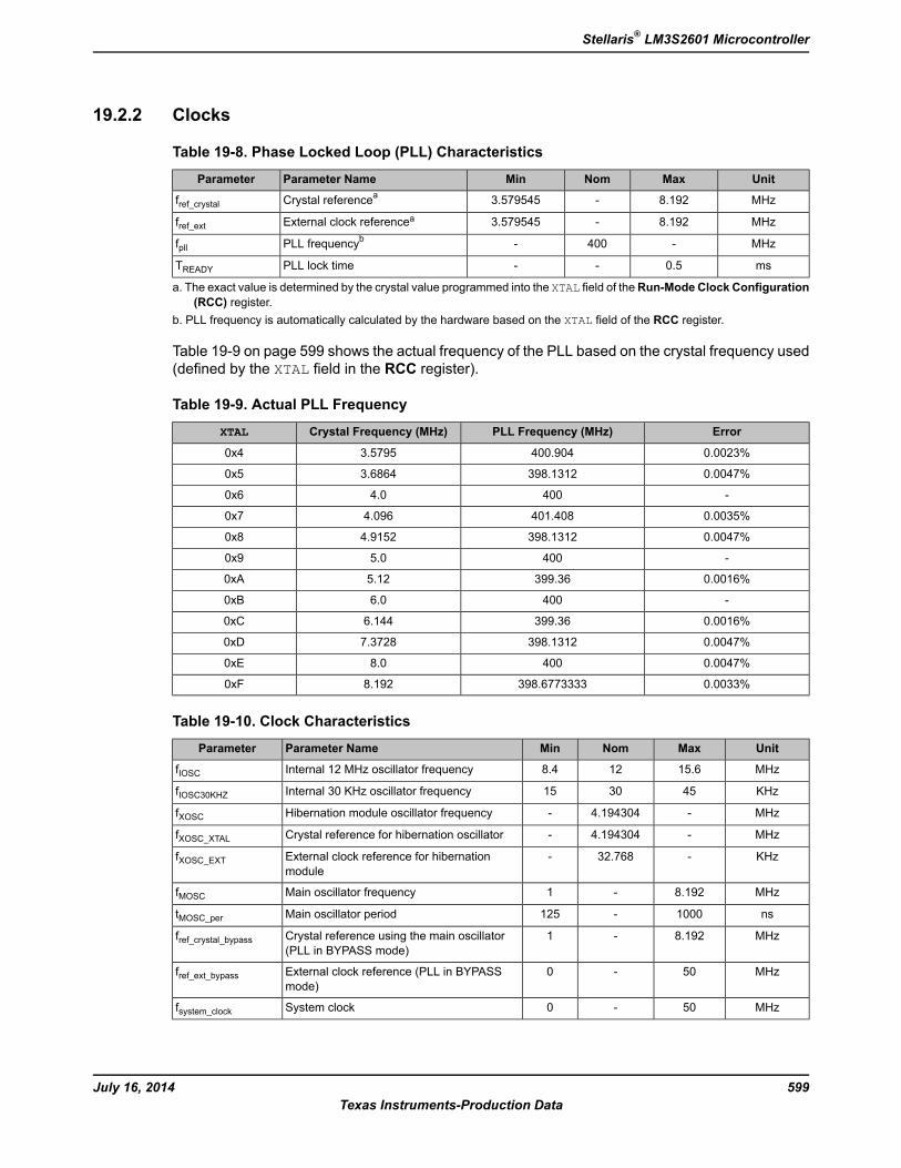
19.2.2 Clocks
Table 19-8. Phase Locked Loop (PLL) Characteristics
UnitMaxNomMinParameter NameParameter
MHz8.192-3.579545Crystal referenceafref_crystalMHz8.192-3.579545External clock referenceafref_extMHz-400-PLL frequencybfpllms0.5--PLL lock timeTREADY
a. The exact value is determined by the crystal value programmed into the XTAL field of theRun-Mode Clock Configuration(RCC) register.
b. PLL frequency is automatically calculated by the hardware based on the XTAL field of the RCC register.
Table 19-9 on page 599 shows the actual frequency of the PLL based on the crystal frequency used(defined by the XTAL field in the RCC register).
Table 19-9. Actual PLL Frequency
ErrorPLL Frequency (MHz)Crystal Frequency (MHz)XTAL
0.0023%400.9043.57950x4
0.0047%398.13123.68640x5
-4004.00x6
0.0035%401.4084.0960x7
0.0047%398.13124.91520x8
-4005.00x9
0.0016%399.365.120xA
-4006.00xB
0.0016%399.366.1440xC
0.0047%398.13127.37280xD
0.0047%4008.00xE
0.0033%398.67733338.1920xF
Table 19-10. Clock Characteristics
UnitMaxNomMinParameter NameParameter
MHz15.6128.4Internal 12 MHz oscillator frequencyfIOSCKHz453015Internal 30 KHz oscillator frequencyfIOSC30KHZMHz-4.194304-Hibernation module oscillator frequencyfXOSCMHz-4.194304-Crystal reference for hibernation oscillatorfXOSC_XTALKHz-32.768-External clock reference for hibernation
modulefXOSC_EXT
MHz8.192-1Main oscillator frequencyfMOSCns1000-125Main oscillator periodtMOSC_perMHz8.192-1Crystal reference using the main oscillator
(PLL in BYPASS mode)fref_crystal_bypass
MHz50-0External clock reference (PLL in BYPASSmode)
fref_ext_bypass
MHz50-0System clockfsystem_clock
599July 16, 2014Texas Instruments-Production Data
Stellaris® LM3S2601 Microcontroller
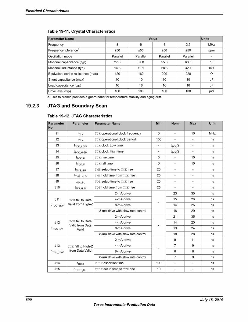
Table 19-11. Crystal Characteristics
UnitsValueParameter Name
MHz3.5468Frequency
ppm±50±50±50±50Frequency tolerancea
-ParallelParallelParallelParallelOscillation mode
pF63.555.637.027.8Motional capacitance (typ)
mH32.728.619.114.3Motional inductance (typ)
Ω220200160120Equivalent series resistance (max)
pF10101010Shunt capacitance (max)
pF16161616Load capacitance (typ)
µW100100100100Drive level (typ)
a. This tolerance provides a guard band for temperature stability and aging drift.
19.2.3 JTAG and Boundary Scan
Table 19-12. JTAG Characteristics
UnitMaxNomMinParameter NameParameterParameterNo.
MHz10-0TCK operational clock frequencyfTCKJ1
ns--100TCK operational clock periodtTCKJ2
ns-tTCK/2-TCK clock Low timetTCK_LOWJ3
ns-tTCK/2-TCK clock High timetTCK_HIGHJ4
ns10-0TCK rise timetTCK_RJ5
ns10-0TCK fall timetTCK_FJ6
ns--20TMS setup time to TCK risetTMS_SUJ7
ns--20TMS hold time from TCK risetTMS_HLDJ8
ns--25TDI setup time to TCK risetTDI_SUJ9
ns--25TDI hold time from TCK risetTDI_HLDJ10
ns3523
-
2-mA drive
TCK fall to DataValid from High-Z
J11t TDO_ZDV
ns26154-mA drive
ns25148-mA drive
ns29188-mA drive with slew rate control
ns3521
-
2-mA driveTCK fall to DataValid from Data
Valid
J12t TDO_DV
ns25144-mA drive
ns24138-mA drive
ns28188-mA drive with slew rate control
ns119
-
2-mA drive
TCK fall to High-Zfrom Data Valid
J13t TDO_DVZ
ns974-mA drive
ns868-mA drive
ns978-mA drive with slew rate control
ns--100TRST assertion timetTRSTJ14
ns--10TRST setup time to TCK risetTRST_SUJ15
July 16, 2014600Texas Instruments-Production Data
Electrical Characteristics

Figure 19-2. JTAG Test Clock Input Timing
TCK
J6 J5
J3 J4
J2
Figure 19-3. JTAG Test Access Port (TAP) Timing
TDO Output Valid
TCK
TDO Output Valid
J12
TDO
TDI
TMS
TDI Input Valid TDI Input Valid
J13
J9 J10
TMS Input Valid
J9 J10
TMS Input Valid
J11
J7 J8J8J7
Figure 19-4. JTAG TRST Timing
TCK
J14 J15
TRST
19.2.4 Reset
Table 19-13. Reset Characteristics
UnitMaxNomMinParameter NameParameterParameterNo.
V-2.0-Reset thresholdVTHR1
V2.952.92.85Brown-Out thresholdVBTHR2
ms-10-Power-On Reset timeoutTPORR3
µs-500-Brown-Out timeoutTBORR4
ms11-6Internal reset timeout after PORTIRPORR5
µs1-0Internal reset timeout after BORaTIRBORR6
601July 16, 2014Texas Instruments-Production Data
Stellaris® LM3S2601 Microcontroller
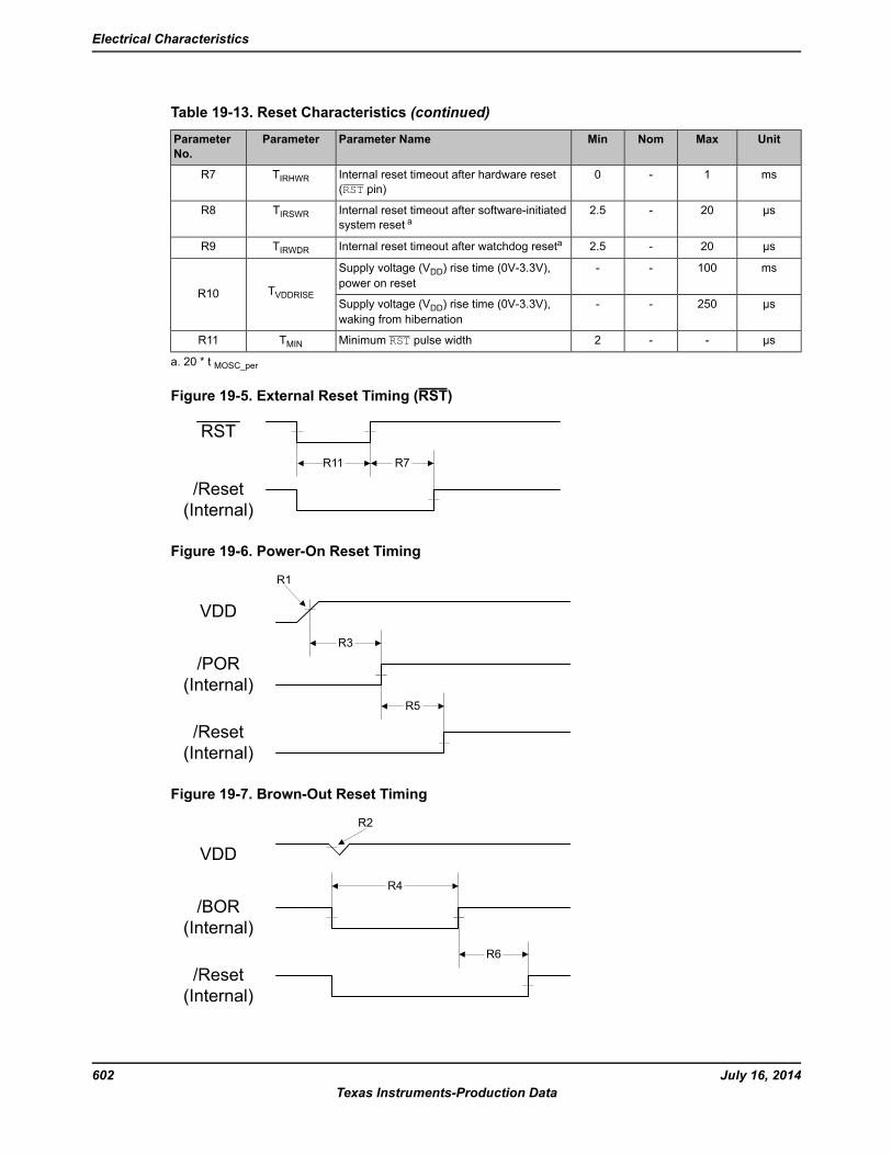
Table 19-13. Reset Characteristics (continued)
UnitMaxNomMinParameter NameParameterParameterNo.
ms1-0Internal reset timeout after hardware reset(RST pin)
TIRHWRR7
µs20-2.5Internal reset timeout after software-initiatedsystem reset a
TIRSWRR8
µs20-2.5Internal reset timeout after watchdog resetaTIRWDRR9
ms100--Supply voltage (VDD) rise time (0V-3.3V),power on reset
TVDDRISER10µs250--Supply voltage (VDD) rise time (0V-3.3V),
waking from hibernation
µs--2Minimum RST pulse widthTMINR11
a. 20 * t MOSC_per
Figure 19-5. External Reset Timing (RST)
RST
/Reset(Internal)
R7R11
Figure 19-6. Power-On Reset Timing
VDD
/POR(Internal)
/Reset(Internal)
R3
R1
R5
Figure 19-7. Brown-Out Reset Timing
VDD
/BOR(Internal)
/Reset(Internal)
R2
R4
R6
July 16, 2014602Texas Instruments-Production Data
Electrical Characteristics
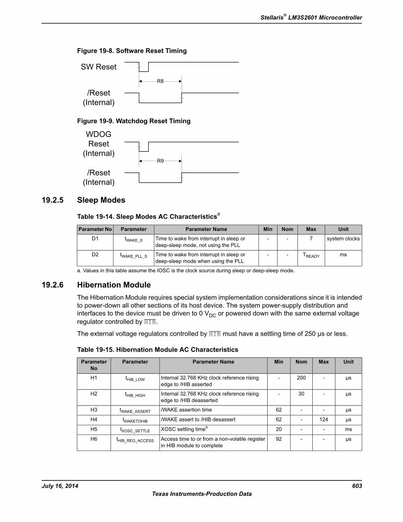
Figure 19-8. Software Reset Timing
R8
SW Reset
/Reset(Internal)
Figure 19-9. Watchdog Reset Timing
WDOGReset
(Internal)
/Reset(Internal)
R9
19.2.5 Sleep Modes
Table 19-14. Sleep Modes AC Characteristicsa
UnitMaxNomMinParameter NameParameterParameter No
system clocks7--Time to wake from interrupt in sleep ordeep-sleep mode, not using the PLL
tWAKE_SD1
msTREADY--Time to wake from interrupt in sleep ordeep-sleep mode when using the PLL
tWAKE_PLL_SD2
a. Values in this table assume the IOSC is the clock source during sleep or deep-sleep mode.
19.2.6 Hibernation ModuleThe Hibernation Module requires special system implementation considerations since it is intendedto power-down all other sections of its host device. The system power-supply distribution andinterfaces to the device must be driven to 0 VDC or powered down with the same external voltageregulator controlled by HIB.
The external voltage regulators controlled by HIB must have a settling time of 250 μs or less.
Table 19-15. Hibernation Module AC Characteristics
UnitMaxNomMinParameter NameParameterParameterNo
μs-200-Internal 32.768 KHz clock reference risingedge to /HIB asserted
tHIB_LOWH1
μs-30-Internal 32.768 KHz clock reference risingedge to /HIB deasserted
tHIB_HIGHH2
μs--62/WAKE assertion timetWAKE_ASSERTH3
μs124-62/WAKE assert to /HIB desasserttWAKETOHIBH4
ms--20XOSC settling timeatXOSC_SETTLEH5
μs--92Access time to or from a non-volatile registerin HIB module to complete
tHIB_REG_ACCESSH6
603July 16, 2014Texas Instruments-Production Data
Stellaris® LM3S2601 Microcontroller
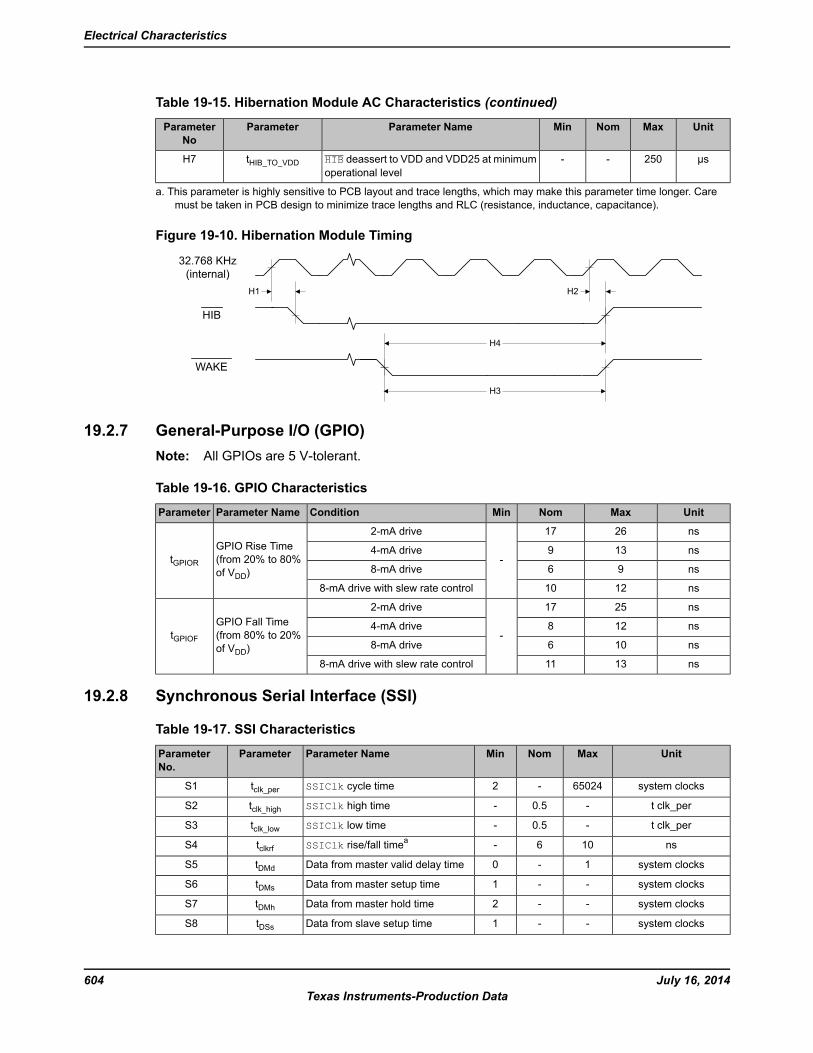
Table 19-15. Hibernation Module AC Characteristics (continued)
UnitMaxNomMinParameter NameParameterParameterNo
μs250--HIB deassert to VDD and VDD25 at minimumoperational level
tHIB_TO_VDDH7
a. This parameter is highly sensitive to PCB layout and trace lengths, which may make this parameter time longer. Caremust be taken in PCB design to minimize trace lengths and RLC (resistance, inductance, capacitance).
Figure 19-10. Hibernation Module Timing
32.768 KHz(internal)
HIB
H4
H1
WAKE
H2
H3
19.2.7 General-Purpose I/O (GPIO)Note: All GPIOs are 5 V-tolerant.
Table 19-16. GPIO Characteristics
UnitMaxNomMinConditionParameter NameParameter
ns2617
-
2-mA driveGPIO Rise Time(from 20% to 80%of VDD)
tGPIORns1394-mA drive
ns968-mA drive
ns12108-mA drive with slew rate control
ns2517
-
2-mA driveGPIO Fall Time(from 80% to 20%of VDD)
tGPIOFns1284-mA drive
ns1068-mA drive
ns13118-mA drive with slew rate control
19.2.8 Synchronous Serial Interface (SSI)
Table 19-17. SSI Characteristics
UnitMaxNomMinParameter NameParameterParameterNo.
system clocks65024-2SSIClk cycle timetclk_perS1
t clk_per-0.5-SSIClk high timetclk_highS2
t clk_per-0.5-SSIClk low timetclk_lowS3
ns106-SSIClk rise/fall timeatclkrfS4
system clocks1-0Data from master valid delay timetDMdS5
system clocks--1Data from master setup timetDMsS6
system clocks--2Data from master hold timetDMhS7
system clocks--1Data from slave setup timetDSsS8
July 16, 2014604Texas Instruments-Production Data
Electrical Characteristics
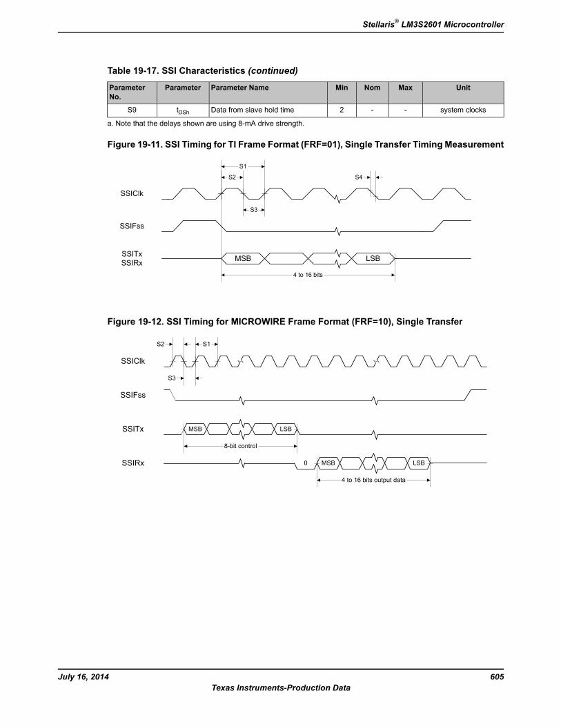
Table 19-17. SSI Characteristics (continued)
UnitMaxNomMinParameter NameParameterParameterNo.
system clocks--2Data from slave hold timetDShS9
a. Note that the delays shown are using 8-mA drive strength.
Figure 19-11. SSI Timing for TI Frame Format (FRF=01), Single Transfer Timing Measurement
SSIClk
SSIFss
SSITxSSIRx MSB LSB
S2
S3
S1
S4
4 to 16 bits
Figure 19-12. SSI Timing for MICROWIRE Frame Format (FRF=10), Single Transfer
0
SSIClk
SSIFss
SSITx
SSIRx
MSB LSB
MSB LSB
S2
S3
S1
8-bit control
4 to 16 bits output data
605July 16, 2014Texas Instruments-Production Data
Stellaris® LM3S2601 Microcontroller
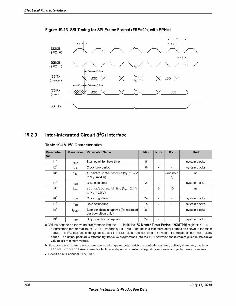
Figure 19-13. SSI Timing for SPI Frame Format (FRF=00), with SPH=1
SSIClk(SPO=1)
SSITx(master)
SSIRx(slave) LSB
SSIClk(SPO=0)
S2
S1
S4
SSIFss
LSB
S3
MSB
S5
S6 S7
S9S8
MSB
19.2.9 Inter-Integrated Circuit (I2C) Interface
Table 19-18. I2C Characteristics
UnitMaxNomMinParameter NameParameterParameterNo.
system clocks--36Start condition hold timetSCHI1a
system clocks--36Clock Low periodtLPI2a
ns(see noteb)
--I2CSCL/I2CSDA rise time (VIL =0.5 Vto V IH =2.4 V)
tSRTI3b
system clocks--2Data hold timetDHI4a
ns109-I2CSCL/I2CSDA fall time (VIH =2.4 Vto V IL =0.5 V)
tSFTI5c
system clocks--24Clock High timetHTI6a
system clocks--18Data setup timetDSI7a
system clocks--36Start condition setup time (for repeatedstart condition only)
tSCSRI8a
system clocks--24Stop condition setup timetSCSI9a
a. Values depend on the value programmed into the TPR bit in the I2C Master Timer Period (I2CMTPR) register; a TPRprogrammed for the maximum I2CSCL frequency (TPR=0x2) results in a minimum output timing as shown in the tableabove. The I 2C interface is designed to scale the actual data transition time to move it to the middle of the I2CSCL Lowperiod. The actual position is affected by the value programmed into the TPR; however, the numbers given in the abovevalues are minimum values.
b. Because I2CSCL and I2CSDA are open-drain-type outputs, which the controller can only actively drive Low, the timeI2CSCL or I2CSDA takes to reach a high level depends on external signal capacitance and pull-up resistor values.
c. Specified at a nominal 50 pF load.
July 16, 2014606Texas Instruments-Production Data
Electrical Characteristics
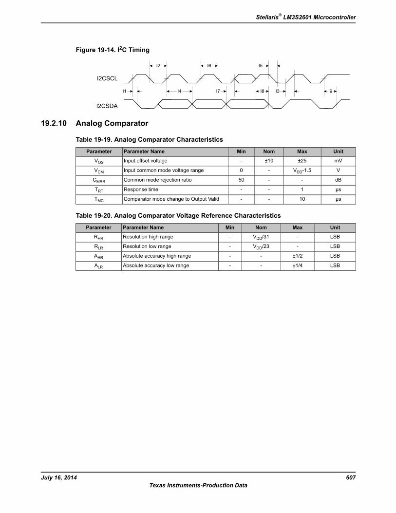
Figure 19-14. I2C Timing
I2CSCL
I2CSDA
I1
I2
I4
I6
I7 I8
I5
I3 I9
19.2.10 Analog Comparator
Table 19-19. Analog Comparator Characteristics
UnitMaxNomMinParameter NameParameter
mV±25±10-Input offset voltageVOSVVDD-1.5-0Input common mode voltage rangeVCMdB--50Common mode rejection ratioCMRR
µs1--Response timeTRTµs10--Comparator mode change to Output ValidTMC
Table 19-20. Analog Comparator Voltage Reference Characteristics
UnitMaxNomMinParameter NameParameter
LSB-VDD/31-Resolution high rangeRHR
LSB-VDD/23-Resolution low rangeRLR
LSB±1/2--Absolute accuracy high rangeAHRLSB±1/4--Absolute accuracy low rangeALR
607July 16, 2014Texas Instruments-Production Data
Stellaris® LM3S2601 Microcontroller
A Serial Flash LoaderA.1 Serial Flash Loader
The Stellaris® serial flash loader is a preprogrammed flash-resident utility used to download codeto the flash memory of a device without the use of a debug interface. The serial flash loader usesa simple packet interface to provide synchronous communication with the device. The flash loaderruns off the crystal and does not enable the PLL, so its speed is determined by the crystal used.The two serial interfaces that can be used are the UART0 and SSI0 interfaces. For simplicity, boththe data format and communication protocol are identical for both serial interfaces.
A.2 InterfacesOnce communication with the flash loader is established via one of the serial interfaces, that interfaceis used until the flash loader is reset or new code takes over. For example, once you startcommunicating using the SSI port, communications with the flash loader via the UART are disableduntil the device is reset.
A.2.1 UARTThe Universal Asynchronous Receivers/Transmitters (UART) communication uses a fixed serialformat of 8 bits of data, no parity, and 1 stop bit. The baud rate used for communication isautomatically detected by the flash loader and can be any valid baud rate supported by the hostand the device. The auto detection sequence requires that the baud rate should be no more than1/32 the crystal frequency of the board that is running the serial flash loader. This is actually thesame as the hardware limitation for the maximum baud rate for any UART on a Stellaris devicewhich is calculated as follows:
Max Baud Rate = System Clock Frequency / 16
In order to determine the baud rate, the serial flash loader needs to determine the relationshipbetween its own crystal frequency and the baud rate. This is enough information for the flash loaderto configure its UART to the same baud rate as the host. This automatic baud-rate detection allowsthe host to use any valid baud rate that it wants to communicate with the device.
The method used to perform this automatic synchronization relies on the host sending the flashloader two bytes that are both 0x55. This generates a series of pulses to the flash loader that it canuse to calculate the ratios needed to program the UART to match the host’s baud rate. After thehost sends the pattern, it attempts to read back one byte of data from the UART. The flash loaderreturns the value of 0xCC to indicate successful detection of the baud rate. If this byte is not receivedafter at least twice the time required to transfer the two bytes, the host can resend another patternof 0x55, 0x55, and wait for the 0xCC byte again until the flash loader acknowledges that it hasreceived a synchronization pattern correctly. For example, the time to wait for data back from theflash loader should be calculated as at least 2*(20(bits/sync)/baud rate (bits/sec)). For a baud rateof 115200, this time is 2*(20/115200) or 0.35 ms.
A.2.2 SSIThe Synchronous Serial Interface (SSI) port also uses a fixed serial format for communications,with the framing defined as Motorola format with SPH set to 1 and SPO set to 1. See “FrameFormats” on page 434 in the SSI chapter for more information on formats for this transfer protocol.Like the UART, this interface has hardware requirements that limit the maximum speed that the SSIclock can run. This allows the SSI clock to be at most 1/12 the crystal frequency of the board running
July 16, 2014608Texas Instruments-Production Data
Serial Flash Loader
the flash loader. Since the host device is the master, the SSI on the flash loader device does notneed to determine the clock as it is provided directly by the host.
A.3 Packet HandlingAll communications, with the exception of the UART auto-baud, are done via defined packets thatare acknowledged (ACK) or not acknowledged (NAK) by the devices. The packets use the sameformat for receiving and sending packets, including the method used to acknowledge successful orunsuccessful reception of a packet.
A.3.1 Packet FormatAll packets sent and received from the device use the following byte-packed format.
struct unsigned char ucSize; unsigned char ucCheckSum; unsigned char Data[];;
ucSize The first byte received holds the total size of the transfer includingthe size and checksum bytes.
ucChecksum This holds a simple checksum of the bytes in the data buffer only.The algorithm is Data[0]+Data[1]+…+ Data[ucSize-3].
Data This is the raw data intended for the device, which is formatted insome form of command interface. There should be ucSize–2bytes of data provided in this buffer to or from the device.
A.3.2 Sending PacketsThe actual bytes of the packet can be sent individually or all at once; the only limitation is thatcommands that cause flash memory access should limit the download sizes to prevent losing bytesduring flash programming. This limitation is discussed further in the section that describes the serialflash loader command, COMMAND_SEND_DATA (see “COMMAND_SEND_DATA(0x24)” on page 611).
Once the packet has been formatted correctly by the host, it should be sent out over the UART orSSI interface. Then the host should poll the UART or SSI interface for the first non-zero data returnedfrom the device. The first non-zero byte will either be an ACK (0xCC) or a NAK (0x33) byte fromthe device indicating the packet was received successfully (ACK) or unsuccessfully (NAK). Thisdoes not indicate that the actual contents of the command issued in the data portion of the packetwere valid, just that the packet was received correctly.
A.3.3 Receiving PacketsThe flash loader sends a packet of data in the same format that it receives a packet. The flash loadermay transfer leading zero data before the first actual byte of data is sent out. The first non-zero byteis the size of the packet followed by a checksum byte, and finally followed by the data itself. Thereis no break in the data after the first non-zero byte is sent from the flash loader. Once the devicecommunicating with the flash loader receives all the bytes, it must either ACK or NAK the packet toindicate that the transmission was successful. The appropriate response after sending a NAK tothe flash loader is to resend the command that failed and request the data again. If needed, thehost may send leading zeros before sending down the ACK/NAK signal to the flash loader, as the
609July 16, 2014Texas Instruments-Production Data
Stellaris® LM3S2601 Microcontroller
flash loader only accepts the first non-zero data as a valid response. This zero padding is neededby the SSI interface in order to receive data to or from the flash loader.
A.4 CommandsThe next section defines the list of commands that can be sent to the flash loader. The first byte ofthe data should always be one of the defined commands, followed by data or parameters asdetermined by the command that is sent.
A.4.1 COMMAND_PING (0X20)This command simply accepts the command and sets the global status to success. The format ofthe packet is as follows:
Byte[0] = 0x03;Byte[1] = checksum(Byte[2]);Byte[2] = COMMAND_PING;
The ping command has 3 bytes and the value for COMMAND_PING is 0x20 and the checksum of onebyte is that same byte, making Byte[1] also 0x20. Since the ping command has no real return status,the receipt of an ACK can be interpreted as a successful ping to the flash loader.
A.4.2 COMMAND_GET_STATUS (0x23)This command returns the status of the last command that was issued. Typically, this commandshould be sent after every command to ensure that the previous command was successful or toproperly respond to a failure. The command requires one byte in the data of the packet and shouldbe followed by reading a packet with one byte of data that contains a status code. The last step isto ACK or NAK the received data so the flash loader knows that the data has been read.
Byte[0] = 0x03Byte[1] = checksum(Byte[2])Byte[2] = COMMAND_GET_STATUS
A.4.3 COMMAND_DOWNLOAD (0x21)This command is sent to the flash loader to indicate where to store data and how many bytes willbe sent by the COMMAND_SEND_DATA commands that follow. The command consists of two 32-bitvalues that are both transferred MSB first. The first 32-bit value is the address to start programmingdata into, while the second is the 32-bit size of the data that will be sent. This command also triggersan erase of the full area to be programmed so this command takes longer than other commands.This results in a longer time to receive the ACK/NAK back from the board. This command shouldbe followed by a COMMAND_GET_STATUS to ensure that the Program Address and Program sizeare valid for the device running the flash loader.
The format of the packet to send this command is a follows:
Byte[0] = 11Byte[1] = checksum(Bytes[2:10])Byte[2] = COMMAND_DOWNLOADByte[3] = Program Address [31:24]Byte[4] = Program Address [23:16]Byte[5] = Program Address [15:8]Byte[6] = Program Address [7:0]Byte[7] = Program Size [31:24]
July 16, 2014610Texas Instruments-Production Data
Serial Flash Loader
Byte[8] = Program Size [23:16]Byte[9] = Program Size [15:8]Byte[10] = Program Size [7:0]
A.4.4 COMMAND_SEND_DATA (0x24)This command should only follow a COMMAND_DOWNLOAD command or anotherCOMMAND_SEND_DATA command if more data is needed. Consecutive send data commandsautomatically increment address and continue programming from the previous location. The callershould limit transfers of data to a maximum 8 bytes of packet data to allow the flash to programsuccessfully and not overflow input buffers of the serial interfaces. The command terminatesprogramming once the number of bytes indicated by the COMMAND_DOWNLOAD command has beenreceived. Each time this function is called it should be followed by a COMMAND_GET_STATUS toensure that the data was successfully programmed into the flash. If the flash loader sends a NAKto this command, the flash loader does not increment the current address to allow retransmissionof the previous data.
Byte[0] = 11Byte[1] = checksum(Bytes[2:10])Byte[2] = COMMAND_SEND_DATAByte[3] = Data[0]Byte[4] = Data[1]Byte[5] = Data[2]Byte[6] = Data[3]Byte[7] = Data[4]Byte[8] = Data[5]Byte[9] = Data[6]Byte[10] = Data[7]
A.4.5 COMMAND_RUN (0x22)This command is used to tell the flash loader to execute from the address passed as the parameterin this command. This command consists of a single 32-bit value that is interpreted as the addressto execute. The 32-bit value is transmitted MSB first and the flash loader responds with an ACKsignal back to the host device before actually executing the code at the given address. This allowsthe host to know that the command was received successfully and the code is now running.
Byte[0] = 7Byte[1] = checksum(Bytes[2:6])Byte[2] = COMMAND_RUNByte[3] = Execute Address[31:24]Byte[4] = Execute Address[23:16]Byte[5] = Execute Address[15:8]Byte[6] = Execute Address[7:0]
A.4.6 COMMAND_RESET (0x25)This command is used to tell the flash loader device to reset. This is useful when downloading anew image that overwrote the flash loader and wants to start from a full reset. Unlike theCOMMAND_RUN command, this allows the initial stack pointer to be read by the hardware and setup for the new code. It can also be used to reset the flash loader if a critical error occurs and thehost device wants to restart communication with the flash loader.
611July 16, 2014Texas Instruments-Production Data
Stellaris® LM3S2601 Microcontroller

Byte[0] = 3Byte[1] = checksum(Byte[2])Byte[2] = COMMAND_RESET
The flash loader responds with an ACK signal back to the host device before actually executing thesoftware reset to the device running the flash loader. This allows the host to know that the commandwas received successfully and the part will be reset.
July 16, 2014612Texas Instruments-Production Data
Serial Flash Loader
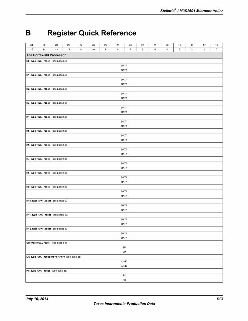
B Register Quick Reference16171819202122232425262728293031
0123456789101112131415
The Cortex-M3 ProcessorR0, type R/W, , reset - (see page 53)
DATA
DATA
R1, type R/W, , reset - (see page 53)
DATA
DATA
R2, type R/W, , reset - (see page 53)
DATA
DATA
R3, type R/W, , reset - (see page 53)
DATA
DATA
R4, type R/W, , reset - (see page 53)
DATA
DATA
R5, type R/W, , reset - (see page 53)
DATA
DATA
R6, type R/W, , reset - (see page 53)
DATA
DATA
R7, type R/W, , reset - (see page 53)
DATA
DATA
R8, type R/W, , reset - (see page 53)
DATA
DATA
R9, type R/W, , reset - (see page 53)
DATA
DATA
R10, type R/W, , reset - (see page 53)
DATA
DATA
R11, type R/W, , reset - (see page 53)
DATA
DATA
R12, type R/W, , reset - (see page 53)
DATA
DATA
SP, type R/W, , reset - (see page 54)
SP
SP
LR, type R/W, , reset 0xFFFF.FFFF (see page 55)
LINK
LINK
PC, type R/W, , reset - (see page 56)
PC
PC
613July 16, 2014Texas Instruments-Production Data
Stellaris® LM3S2601 Microcontroller
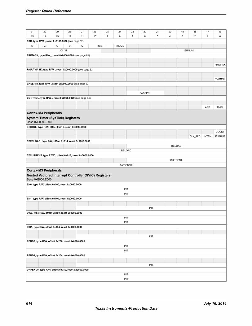
16171819202122232425262728293031
0123456789101112131415
PSR, type R/W, , reset 0x0100.0000 (see page 57)
THUMBICI / ITQVCZN
ISRNUMICI / IT
PRIMASK, type R/W, , reset 0x0000.0000 (see page 61)
PRIMASK
FAULTMASK, type R/W, , reset 0x0000.0000 (see page 62)
FAULTMASK
BASEPRI, type R/W, , reset 0x0000.0000 (see page 63)
BASEPRI
CONTROL, type R/W, , reset 0x0000.0000 (see page 64)
TMPLASP
Cortex-M3 PeripheralsSystem Timer (SysTick) RegistersBase 0xE000.E000
STCTRL, type R/W, offset 0x010, reset 0x0000.0000
COUNT
ENABLEINTENCLK_SRC
STRELOAD, type R/W, offset 0x014, reset 0x0000.0000
RELOAD
RELOAD
STCURRENT, type R/WC, offset 0x018, reset 0x0000.0000
CURRENT
CURRENT
Cortex-M3 PeripheralsNested Vectored Interrupt Controller (NVIC) RegistersBase 0xE000.E000
EN0, type R/W, offset 0x100, reset 0x0000.0000
INT
INT
EN1, type R/W, offset 0x104, reset 0x0000.0000
INT
DIS0, type R/W, offset 0x180, reset 0x0000.0000
INT
INT
DIS1, type R/W, offset 0x184, reset 0x0000.0000
INT
PEND0, type R/W, offset 0x200, reset 0x0000.0000
INT
INT
PEND1, type R/W, offset 0x204, reset 0x0000.0000
INT
UNPEND0, type R/W, offset 0x280, reset 0x0000.0000
INT
INT
July 16, 2014614Texas Instruments-Production Data
Register Quick Reference
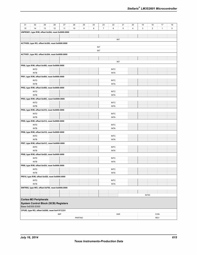
16171819202122232425262728293031
0123456789101112131415
UNPEND1, type R/W, offset 0x284, reset 0x0000.0000
INT
ACTIVE0, type RO, offset 0x300, reset 0x0000.0000
INT
INT
ACTIVE1, type RO, offset 0x304, reset 0x0000.0000
INT
PRI0, type R/W, offset 0x400, reset 0x0000.0000
INTCINTD
INTAINTB
PRI1, type R/W, offset 0x404, reset 0x0000.0000
INTCINTD
INTAINTB
PRI2, type R/W, offset 0x408, reset 0x0000.0000
INTCINTD
INTAINTB
PRI3, type R/W, offset 0x40C, reset 0x0000.0000
INTCINTD
INTAINTB
PRI4, type R/W, offset 0x410, reset 0x0000.0000
INTCINTD
INTAINTB
PRI5, type R/W, offset 0x414, reset 0x0000.0000
INTCINTD
INTAINTB
PRI6, type R/W, offset 0x418, reset 0x0000.0000
INTCINTD
INTAINTB
PRI7, type R/W, offset 0x41C, reset 0x0000.0000
INTCINTD
INTAINTB
PRI8, type R/W, offset 0x420, reset 0x0000.0000
INTCINTD
INTAINTB
PRI9, type R/W, offset 0x424, reset 0x0000.0000
INTCINTD
INTAINTB
PRI10, type R/W, offset 0x428, reset 0x0000.0000
INTCINTD
INTAINTB
SWTRIG, type WO, offset 0xF00, reset 0x0000.0000
INTID
Cortex-M3 PeripheralsSystem Control Block (SCB) RegistersBase 0xE000.E000
CPUID, type RO, offset 0xD00, reset 0x411F.C231
CONVARIMP
REVPARTNO
615July 16, 2014Texas Instruments-Production Data
Stellaris® LM3S2601 Microcontroller
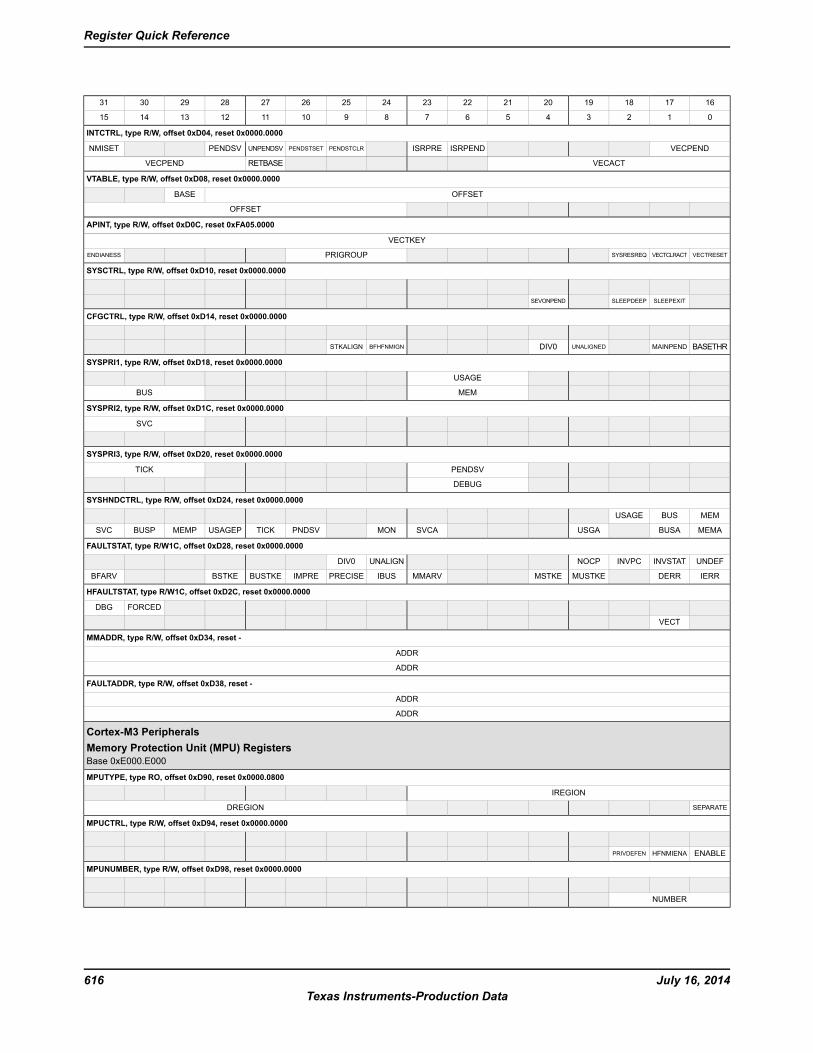
16171819202122232425262728293031
0123456789101112131415
INTCTRL, type R/W, offset 0xD04, reset 0x0000.0000
VECPENDISRPENDISRPREPENDSTCLRPENDSTSETUNPENDSVPENDSVNMISET
VECACTRETBASEVECPEND
VTABLE, type R/W, offset 0xD08, reset 0x0000.0000
OFFSETBASE
OFFSET
APINT, type R/W, offset 0xD0C, reset 0xFA05.0000
VECTKEY
VECTRESETVECTCLRACTSYSRESREQPRIGROUPENDIANESS
SYSCTRL, type R/W, offset 0xD10, reset 0x0000.0000
SLEEPEXITSLEEPDEEPSEVONPEND
CFGCTRL, type R/W, offset 0xD14, reset 0x0000.0000
BASETHRMAINPENDUNALIGNEDDIV0BFHFNMIGNSTKALIGN
SYSPRI1, type R/W, offset 0xD18, reset 0x0000.0000
USAGE
MEMBUS
SYSPRI2, type R/W, offset 0xD1C, reset 0x0000.0000
SVC
SYSPRI3, type R/W, offset 0xD20, reset 0x0000.0000
PENDSVTICK
DEBUG
SYSHNDCTRL, type R/W, offset 0xD24, reset 0x0000.0000
MEMBUSUSAGE
MEMABUSAUSGASVCAMONPNDSVTICKUSAGEPMEMPBUSPSVC
FAULTSTAT, type R/W1C, offset 0xD28, reset 0x0000.0000
UNDEFINVSTATINVPCNOCPUNALIGNDIV0
IERRDERRMUSTKEMSTKEMMARVIBUSPRECISEIMPREBUSTKEBSTKEBFARV
HFAULTSTAT, type R/W1C, offset 0xD2C, reset 0x0000.0000
FORCEDDBG
VECT
MMADDR, type R/W, offset 0xD34, reset -
ADDR
ADDR
FAULTADDR, type R/W, offset 0xD38, reset -
ADDR
ADDR
Cortex-M3 PeripheralsMemory Protection Unit (MPU) RegistersBase 0xE000.E000
MPUTYPE, type RO, offset 0xD90, reset 0x0000.0800
IREGION
SEPARATEDREGION
MPUCTRL, type R/W, offset 0xD94, reset 0x0000.0000
ENABLEHFNMIENAPRIVDEFEN
MPUNUMBER, type R/W, offset 0xD98, reset 0x0000.0000
NUMBER
July 16, 2014616Texas Instruments-Production Data
Register Quick Reference
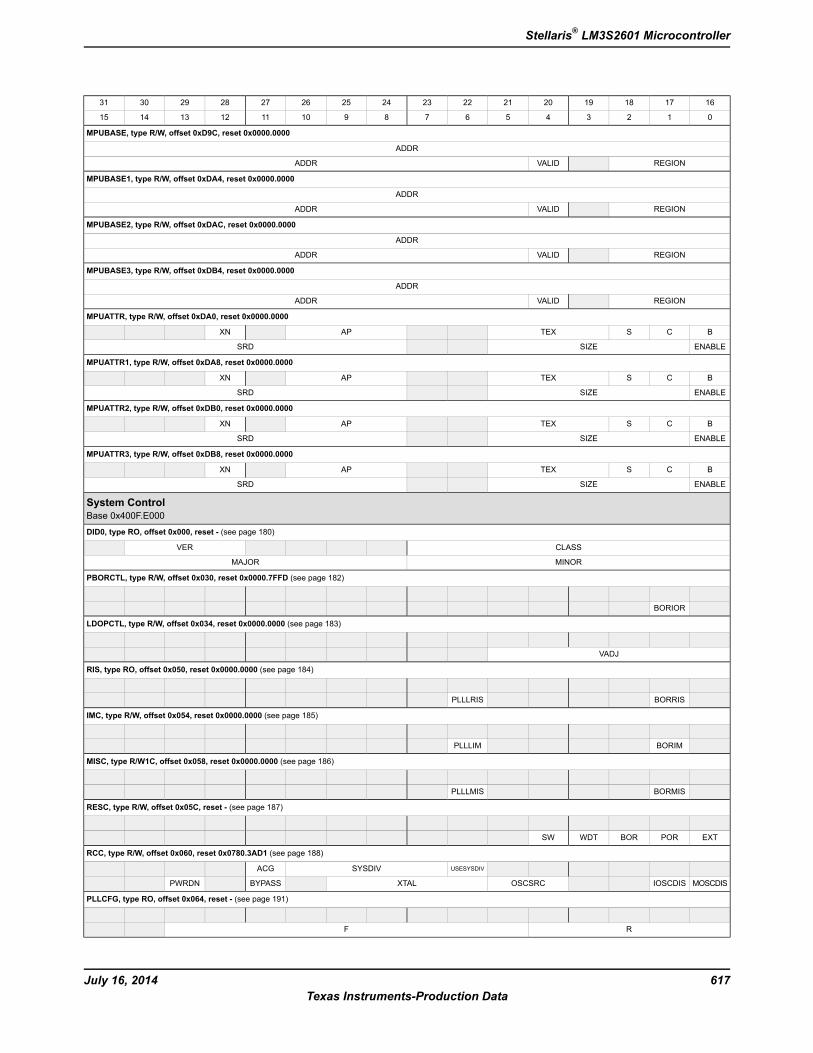
16171819202122232425262728293031
0123456789101112131415
MPUBASE, type R/W, offset 0xD9C, reset 0x0000.0000
ADDR
REGIONVALIDADDR
MPUBASE1, type R/W, offset 0xDA4, reset 0x0000.0000
ADDR
REGIONVALIDADDR
MPUBASE2, type R/W, offset 0xDAC, reset 0x0000.0000
ADDR
REGIONVALIDADDR
MPUBASE3, type R/W, offset 0xDB4, reset 0x0000.0000
ADDR
REGIONVALIDADDR
MPUATTR, type R/W, offset 0xDA0, reset 0x0000.0000
BCSTEXAPXN
ENABLESIZESRD
MPUATTR1, type R/W, offset 0xDA8, reset 0x0000.0000
BCSTEXAPXN
ENABLESIZESRD
MPUATTR2, type R/W, offset 0xDB0, reset 0x0000.0000
BCSTEXAPXN
ENABLESIZESRD
MPUATTR3, type R/W, offset 0xDB8, reset 0x0000.0000
BCSTEXAPXN
ENABLESIZESRD
System ControlBase 0x400F.E000
DID0, type RO, offset 0x000, reset - (see page 180)
CLASSVER
MINORMAJOR
PBORCTL, type R/W, offset 0x030, reset 0x0000.7FFD (see page 182)
BORIOR
LDOPCTL, type R/W, offset 0x034, reset 0x0000.0000 (see page 183)
VADJ
RIS, type RO, offset 0x050, reset 0x0000.0000 (see page 184)
BORRISPLLLRIS
IMC, type R/W, offset 0x054, reset 0x0000.0000 (see page 185)
BORIMPLLLIM
MISC, type R/W1C, offset 0x058, reset 0x0000.0000 (see page 186)
BORMISPLLLMIS
RESC, type R/W, offset 0x05C, reset - (see page 187)
EXTPORBORWDTSW
RCC, type R/W, offset 0x060, reset 0x0780.3AD1 (see page 188)
USESYSDIVSYSDIVACG
MOSCDISIOSCDISOSCSRCXTALBYPASSPWRDN
PLLCFG, type RO, offset 0x064, reset - (see page 191)
RF
617July 16, 2014Texas Instruments-Production Data
Stellaris® LM3S2601 Microcontroller
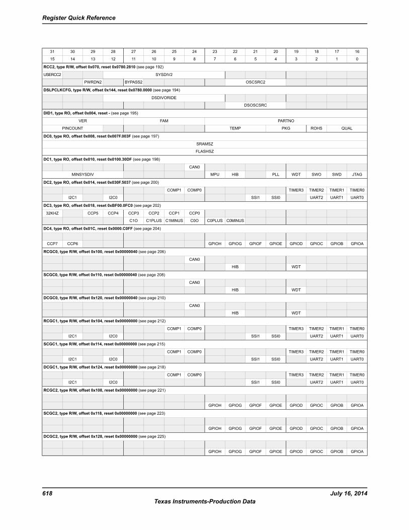
16171819202122232425262728293031
0123456789101112131415
RCC2, type R/W, offset 0x070, reset 0x0780.2810 (see page 192)
SYSDIV2USERCC2
OSCSRC2BYPASS2PWRDN2
DSLPCLKCFG, type R/W, offset 0x144, reset 0x0780.0000 (see page 194)
DSDIVORIDE
DSOSCSRC
DID1, type RO, offset 0x004, reset - (see page 195)
PARTNOFAMVER
QUALROHSPKGTEMPPINCOUNT
DC0, type RO, offset 0x008, reset 0x007F.003F (see page 197)
SRAMSZ
FLASHSZ
DC1, type RO, offset 0x010, reset 0x0100.30DF (see page 198)
CAN0
JTAGSWDSWOWDTPLLHIBMPUMINSYSDIV
DC2, type RO, offset 0x014, reset 0x030F.5037 (see page 200)
TIMER0TIMER1TIMER2TIMER3COMP0COMP1
UART0UART1UART2SSI0SSI1I2C0I2C1
DC3, type RO, offset 0x018, reset 0xBF00.0FC0 (see page 202)
CCP0CCP1CCP2CCP3CCP4CCP532KHZ
C0MINUSC0PLUSC0OC1MINUSC1PLUSC1O
DC4, type RO, offset 0x01C, reset 0x0000.C0FF (see page 204)
GPIOAGPIOBGPIOCGPIODGPIOEGPIOFGPIOGGPIOHCCP6CCP7
RCGC0, type R/W, offset 0x100, reset 0x00000040 (see page 206)
CAN0
WDTHIB
SCGC0, type R/W, offset 0x110, reset 0x00000040 (see page 208)
CAN0
WDTHIB
DCGC0, type R/W, offset 0x120, reset 0x00000040 (see page 210)
CAN0
WDTHIB
RCGC1, type R/W, offset 0x104, reset 0x00000000 (see page 212)
TIMER0TIMER1TIMER2TIMER3COMP0COMP1
UART0UART1UART2SSI0SSI1I2C0I2C1
SCGC1, type R/W, offset 0x114, reset 0x00000000 (see page 215)
TIMER0TIMER1TIMER2TIMER3COMP0COMP1
UART0UART1UART2SSI0SSI1I2C0I2C1
DCGC1, type R/W, offset 0x124, reset 0x00000000 (see page 218)
TIMER0TIMER1TIMER2TIMER3COMP0COMP1
UART0UART1UART2SSI0SSI1I2C0I2C1
RCGC2, type R/W, offset 0x108, reset 0x00000000 (see page 221)
GPIOAGPIOBGPIOCGPIODGPIOEGPIOFGPIOGGPIOH
SCGC2, type R/W, offset 0x118, reset 0x00000000 (see page 223)
GPIOAGPIOBGPIOCGPIODGPIOEGPIOFGPIOGGPIOH
DCGC2, type R/W, offset 0x128, reset 0x00000000 (see page 225)
GPIOAGPIOBGPIOCGPIODGPIOEGPIOFGPIOGGPIOH
July 16, 2014618Texas Instruments-Production Data
Register Quick Reference
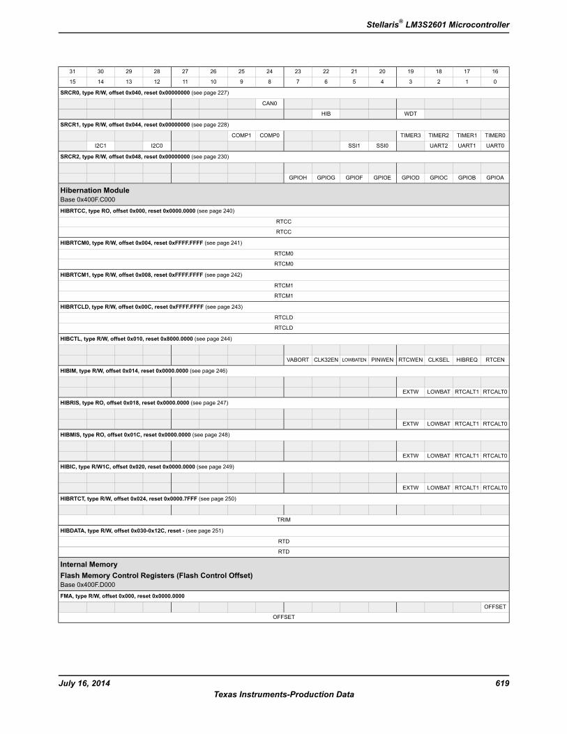
16171819202122232425262728293031
0123456789101112131415
SRCR0, type R/W, offset 0x040, reset 0x00000000 (see page 227)
CAN0
WDTHIB
SRCR1, type R/W, offset 0x044, reset 0x00000000 (see page 228)
TIMER0TIMER1TIMER2TIMER3COMP0COMP1
UART0UART1UART2SSI0SSI1I2C0I2C1
SRCR2, type R/W, offset 0x048, reset 0x00000000 (see page 230)
GPIOAGPIOBGPIOCGPIODGPIOEGPIOFGPIOGGPIOH
Hibernation ModuleBase 0x400F.C000
HIBRTCC, type RO, offset 0x000, reset 0x0000.0000 (see page 240)
RTCC
RTCC
HIBRTCM0, type R/W, offset 0x004, reset 0xFFFF.FFFF (see page 241)
RTCM0
RTCM0
HIBRTCM1, type R/W, offset 0x008, reset 0xFFFF.FFFF (see page 242)
RTCM1
RTCM1
HIBRTCLD, type R/W, offset 0x00C, reset 0xFFFF.FFFF (see page 243)
RTCLD
RTCLD
HIBCTL, type R/W, offset 0x010, reset 0x8000.0000 (see page 244)
RTCENHIBREQCLKSELRTCWENPINWENLOWBATENCLK32ENVABORT
HIBIM, type R/W, offset 0x014, reset 0x0000.0000 (see page 246)
RTCALT0RTCALT1LOWBATEXTW
HIBRIS, type RO, offset 0x018, reset 0x0000.0000 (see page 247)
RTCALT0RTCALT1LOWBATEXTW
HIBMIS, type RO, offset 0x01C, reset 0x0000.0000 (see page 248)
RTCALT0RTCALT1LOWBATEXTW
HIBIC, type R/W1C, offset 0x020, reset 0x0000.0000 (see page 249)
RTCALT0RTCALT1LOWBATEXTW
HIBRTCT, type R/W, offset 0x024, reset 0x0000.7FFF (see page 250)
TRIM
HIBDATA, type R/W, offset 0x030-0x12C, reset - (see page 251)
RTD
RTD
Internal MemoryFlash Memory Control Registers (Flash Control Offset)Base 0x400F.D000
FMA, type R/W, offset 0x000, reset 0x0000.0000
OFFSET
OFFSET
619July 16, 2014Texas Instruments-Production Data
Stellaris® LM3S2601 Microcontroller
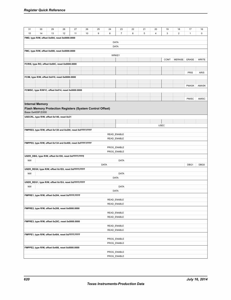
16171819202122232425262728293031
0123456789101112131415
FMD, type R/W, offset 0x004, reset 0x0000.0000
DATA
DATA
FMC, type R/W, offset 0x008, reset 0x0000.0000
WRKEY
WRITEERASEMERASECOMT
FCRIS, type RO, offset 0x00C, reset 0x0000.0000
ARISPRIS
FCIM, type R/W, offset 0x010, reset 0x0000.0000
AMASKPMASK
FCMISC, type R/W1C, offset 0x014, reset 0x0000.0000
AMISCPMISC
Internal MemoryFlash Memory Protection Registers (System Control Offset)Base 0x400F.E000
USECRL, type R/W, offset 0x140, reset 0x31
USEC
FMPRE0, type R/W, offset 0x130 and 0x200, reset 0xFFFF.FFFF
READ_ENABLE
READ_ENABLE
FMPPE0, type R/W, offset 0x134 and 0x400, reset 0xFFFF.FFFF
PROG_ENABLE
PROG_ENABLE
USER_DBG, type R/W, offset 0x1D0, reset 0xFFFF.FFFE
DATANW
DBG0DBG1DATA
USER_REG0, type R/W, offset 0x1E0, reset 0xFFFF.FFFF
DATANW
DATA
USER_REG1, type R/W, offset 0x1E4, reset 0xFFFF.FFFF
DATANW
DATA
FMPRE1, type R/W, offset 0x204, reset 0xFFFF.FFFF
READ_ENABLE
READ_ENABLE
FMPRE2, type R/W, offset 0x208, reset 0x0000.0000
READ_ENABLE
READ_ENABLE
FMPRE3, type R/W, offset 0x20C, reset 0x0000.0000
READ_ENABLE
READ_ENABLE
FMPPE1, type R/W, offset 0x404, reset 0xFFFF.FFFF
PROG_ENABLE
PROG_ENABLE
FMPPE2, type R/W, offset 0x408, reset 0x0000.0000
PROG_ENABLE
PROG_ENABLE
July 16, 2014620Texas Instruments-Production Data
Register Quick Reference
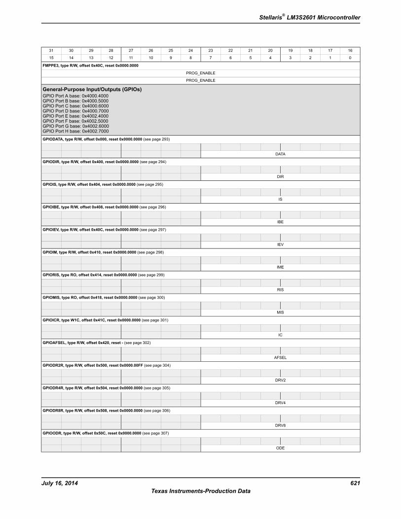
16171819202122232425262728293031
0123456789101112131415
FMPPE3, type R/W, offset 0x40C, reset 0x0000.0000
PROG_ENABLE
PROG_ENABLE
General-Purpose Input/Outputs (GPIOs)GPIO Port A base: 0x4000.4000GPIO Port B base: 0x4000.5000GPIO Port C base: 0x4000.6000GPIO Port D base: 0x4000.7000GPIO Port E base: 0x4002.4000GPIO Port F base: 0x4002.5000GPIO Port G base: 0x4002.6000GPIO Port H base: 0x4002.7000
GPIODATA, type R/W, offset 0x000, reset 0x0000.0000 (see page 293)
DATA
GPIODIR, type R/W, offset 0x400, reset 0x0000.0000 (see page 294)
DIR
GPIOIS, type R/W, offset 0x404, reset 0x0000.0000 (see page 295)
IS
GPIOIBE, type R/W, offset 0x408, reset 0x0000.0000 (see page 296)
IBE
GPIOIEV, type R/W, offset 0x40C, reset 0x0000.0000 (see page 297)
IEV
GPIOIM, type R/W, offset 0x410, reset 0x0000.0000 (see page 298)
IME
GPIORIS, type RO, offset 0x414, reset 0x0000.0000 (see page 299)
RIS
GPIOMIS, type RO, offset 0x418, reset 0x0000.0000 (see page 300)
MIS
GPIOICR, type W1C, offset 0x41C, reset 0x0000.0000 (see page 301)
IC
GPIOAFSEL, type R/W, offset 0x420, reset - (see page 302)
AFSEL
GPIODR2R, type R/W, offset 0x500, reset 0x0000.00FF (see page 304)
DRV2
GPIODR4R, type R/W, offset 0x504, reset 0x0000.0000 (see page 305)
DRV4
GPIODR8R, type R/W, offset 0x508, reset 0x0000.0000 (see page 306)
DRV8
GPIOODR, type R/W, offset 0x50C, reset 0x0000.0000 (see page 307)
ODE
621July 16, 2014Texas Instruments-Production Data
Stellaris® LM3S2601 Microcontroller
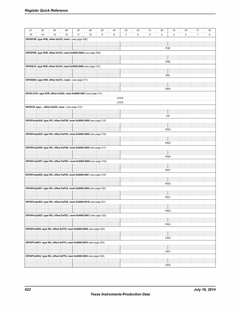
16171819202122232425262728293031
0123456789101112131415
GPIOPUR, type R/W, offset 0x510, reset - (see page 308)
PUE
GPIOPDR, type R/W, offset 0x514, reset 0x0000.0000 (see page 309)
PDE
GPIOSLR, type R/W, offset 0x518, reset 0x0000.0000 (see page 310)
SRL
GPIODEN, type R/W, offset 0x51C, reset - (see page 311)
DEN
GPIOLOCK, type R/W, offset 0x520, reset 0x0000.0001 (see page 312)
LOCK
LOCK
GPIOCR, type -, offset 0x524, reset - (see page 313)
CR
GPIOPeriphID4, type RO, offset 0xFD0, reset 0x0000.0000 (see page 315)
PID4
GPIOPeriphID5, type RO, offset 0xFD4, reset 0x0000.0000 (see page 316)
PID5
GPIOPeriphID6, type RO, offset 0xFD8, reset 0x0000.0000 (see page 317)
PID6
GPIOPeriphID7, type RO, offset 0xFDC, reset 0x0000.0000 (see page 318)
PID7
GPIOPeriphID0, type RO, offset 0xFE0, reset 0x0000.0061 (see page 319)
PID0
GPIOPeriphID1, type RO, offset 0xFE4, reset 0x0000.0000 (see page 320)
PID1
GPIOPeriphID2, type RO, offset 0xFE8, reset 0x0000.0018 (see page 321)
PID2
GPIOPeriphID3, type RO, offset 0xFEC, reset 0x0000.0001 (see page 322)
PID3
GPIOPCellID0, type RO, offset 0xFF0, reset 0x0000.000D (see page 323)
CID0
GPIOPCellID1, type RO, offset 0xFF4, reset 0x0000.00F0 (see page 324)
CID1
GPIOPCellID2, type RO, offset 0xFF8, reset 0x0000.0005 (see page 325)
CID2
July 16, 2014622Texas Instruments-Production Data
Register Quick Reference
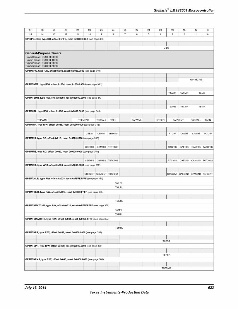
16171819202122232425262728293031
0123456789101112131415
GPIOPCellID3, type RO, offset 0xFFC, reset 0x0000.00B1 (see page 326)
CID3
General-Purpose TimersTimer0 base: 0x4003.0000Timer1 base: 0x4003.1000Timer2 base: 0x4003.2000Timer3 base: 0x4003.3000
GPTMCFG, type R/W, offset 0x000, reset 0x0000.0000 (see page 340)
GPTMCFG
GPTMTAMR, type R/W, offset 0x004, reset 0x0000.0000 (see page 341)
TAMRTACMRTAAMS
GPTMTBMR, type R/W, offset 0x008, reset 0x0000.0000 (see page 343)
TBMRTBCMRTBAMS
GPTMCTL, type R/W, offset 0x00C, reset 0x0000.0000 (see page 345)
TAENTASTALLTAEVENTRTCENTAPWMLTBENTBSTALLTBEVENTTBPWML
GPTMIMR, type R/W, offset 0x018, reset 0x0000.0000 (see page 348)
TATOIMCAMIMCAEIMRTCIMTBTOIMCBMIMCBEIM
GPTMRIS, type RO, offset 0x01C, reset 0x0000.0000 (see page 350)
TATORISCAMRISCAERISRTCRISTBTORISCBMRISCBERIS
GPTMMIS, type RO, offset 0x020, reset 0x0000.0000 (see page 351)
TATOMISCAMMISCAEMISRTCMISTBTOMISCBMMISCBEMIS
GPTMICR, type W1C, offset 0x024, reset 0x0000.0000 (see page 352)
TATOCINTCAMCINTCAECINTRTCCINTTBTOCINTCBMCINTCBECINT
GPTMTAILR, type R/W, offset 0x028, reset 0xFFFF.FFFF (see page 354)
TAILRH
TAILRL
GPTMTBILR, type R/W, offset 0x02C, reset 0x0000.FFFF (see page 355)
TBILRL
GPTMTAMATCHR, type R/W, offset 0x030, reset 0xFFFF.FFFF (see page 356)
TAMRH
TAMRL
GPTMTBMATCHR, type R/W, offset 0x034, reset 0x0000.FFFF (see page 357)
TBMRL
GPTMTAPR, type R/W, offset 0x038, reset 0x0000.0000 (see page 358)
TAPSR
GPTMTBPR, type R/W, offset 0x03C, reset 0x0000.0000 (see page 359)
TBPSR
GPTMTAPMR, type R/W, offset 0x040, reset 0x0000.0000 (see page 360)
TAPSMR
623July 16, 2014Texas Instruments-Production Data
Stellaris® LM3S2601 Microcontroller
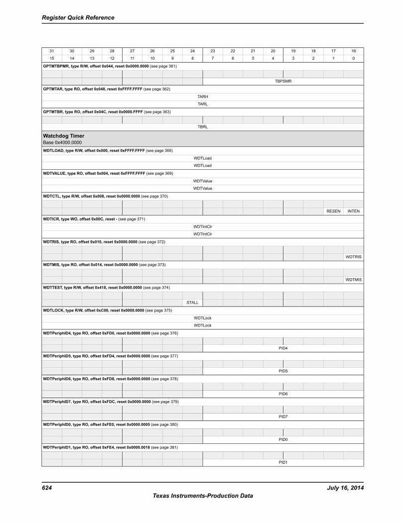
16171819202122232425262728293031
0123456789101112131415
GPTMTBPMR, type R/W, offset 0x044, reset 0x0000.0000 (see page 361)
TBPSMR
GPTMTAR, type RO, offset 0x048, reset 0xFFFF.FFFF (see page 362)
TARH
TARL
GPTMTBR, type RO, offset 0x04C, reset 0x0000.FFFF (see page 363)
TBRL
Watchdog TimerBase 0x4000.0000
WDTLOAD, type R/W, offset 0x000, reset 0xFFFF.FFFF (see page 368)
WDTLoad
WDTLoad
WDTVALUE, type RO, offset 0x004, reset 0xFFFF.FFFF (see page 369)
WDTValue
WDTValue
WDTCTL, type R/W, offset 0x008, reset 0x0000.0000 (see page 370)
INTENRESEN
WDTICR, type WO, offset 0x00C, reset - (see page 371)
WDTIntClr
WDTIntClr
WDTRIS, type RO, offset 0x010, reset 0x0000.0000 (see page 372)
WDTRIS
WDTMIS, type RO, offset 0x014, reset 0x0000.0000 (see page 373)
WDTMIS
WDTTEST, type R/W, offset 0x418, reset 0x0000.0000 (see page 374)
STALL
WDTLOCK, type R/W, offset 0xC00, reset 0x0000.0000 (see page 375)
WDTLock
WDTLock
WDTPeriphID4, type RO, offset 0xFD0, reset 0x0000.0000 (see page 376)
PID4
WDTPeriphID5, type RO, offset 0xFD4, reset 0x0000.0000 (see page 377)
PID5
WDTPeriphID6, type RO, offset 0xFD8, reset 0x0000.0000 (see page 378)
PID6
WDTPeriphID7, type RO, offset 0xFDC, reset 0x0000.0000 (see page 379)
PID7
WDTPeriphID0, type RO, offset 0xFE0, reset 0x0000.0005 (see page 380)
PID0
WDTPeriphID1, type RO, offset 0xFE4, reset 0x0000.0018 (see page 381)
PID1
July 16, 2014624Texas Instruments-Production Data
Register Quick Reference
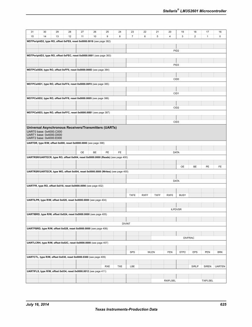
16171819202122232425262728293031
0123456789101112131415
WDTPeriphID2, type RO, offset 0xFE8, reset 0x0000.0018 (see page 382)
PID2
WDTPeriphID3, type RO, offset 0xFEC, reset 0x0000.0001 (see page 383)
PID3
WDTPCellID0, type RO, offset 0xFF0, reset 0x0000.000D (see page 384)
CID0
WDTPCellID1, type RO, offset 0xFF4, reset 0x0000.00F0 (see page 385)
CID1
WDTPCellID2, type RO, offset 0xFF8, reset 0x0000.0005 (see page 386)
CID2
WDTPCellID3, type RO, offset 0xFFC, reset 0x0000.00B1 (see page 387)
CID3
Universal Asynchronous Receivers/Transmitters (UARTs)UART0 base: 0x4000.C000UART1 base: 0x4000.D000UART2 base: 0x4000.E000
UARTDR, type R/W, offset 0x000, reset 0x0000.0000 (see page 398)
DATAFEPEBEOE
UARTRSR/UARTECR, type RO, offset 0x004, reset 0x0000.0000 (Reads) (see page 400)
FEPEBEOE
UARTRSR/UARTECR, type WO, offset 0x004, reset 0x0000.0000 (Writes) (see page 400)
DATA
UARTFR, type RO, offset 0x018, reset 0x0000.0090 (see page 402)
BUSYRXFETXFFRXFFTXFE
UARTILPR, type R/W, offset 0x020, reset 0x0000.0000 (see page 404)
ILPDVSR
UARTIBRD, type R/W, offset 0x024, reset 0x0000.0000 (see page 405)
DIVINT
UARTFBRD, type R/W, offset 0x028, reset 0x0000.0000 (see page 406)
DIVFRAC
UARTLCRH, type R/W, offset 0x02C, reset 0x0000.0000 (see page 407)
BRKPENEPSSTP2FENWLENSPS
UARTCTL, type R/W, offset 0x030, reset 0x0000.0300 (see page 409)
UARTENSIRENSIRLPLBETXERXE
UARTIFLS, type R/W, offset 0x034, reset 0x0000.0012 (see page 411)
TXIFLSELRXIFLSEL
625July 16, 2014Texas Instruments-Production Data
Stellaris® LM3S2601 Microcontroller
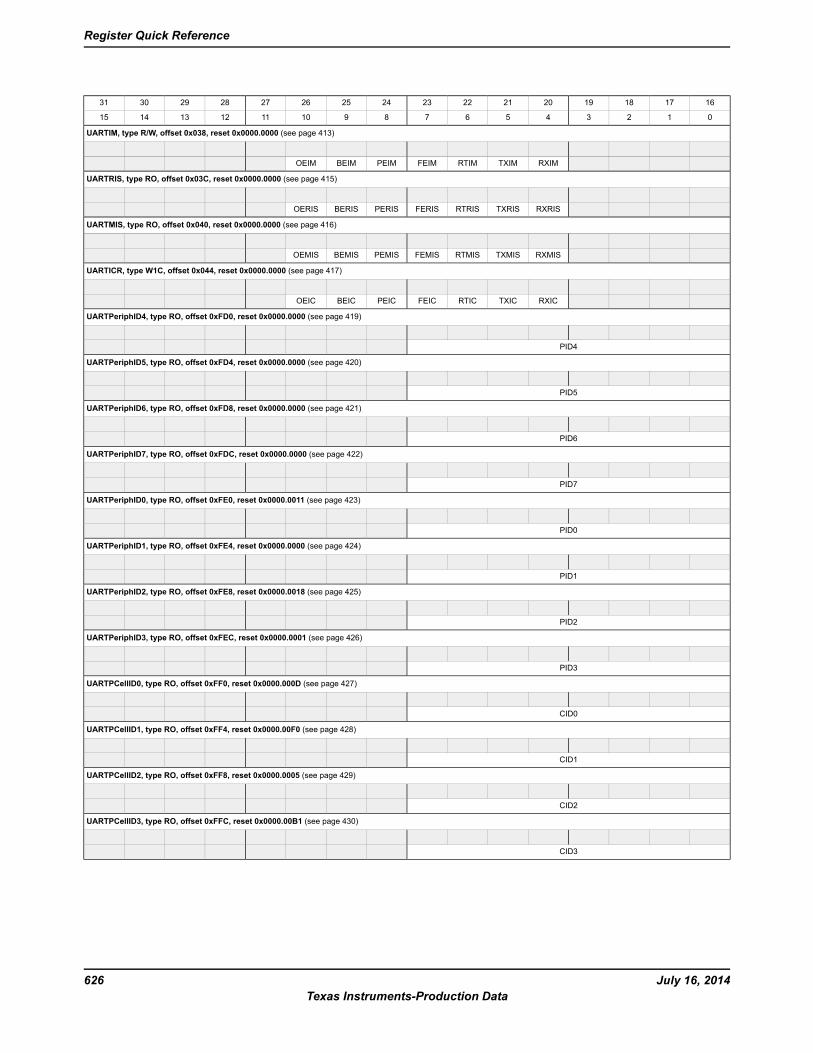
16171819202122232425262728293031
0123456789101112131415
UARTIM, type R/W, offset 0x038, reset 0x0000.0000 (see page 413)
RXIMTXIMRTIMFEIMPEIMBEIMOEIM
UARTRIS, type RO, offset 0x03C, reset 0x0000.0000 (see page 415)
RXRISTXRISRTRISFERISPERISBERISOERIS
UARTMIS, type RO, offset 0x040, reset 0x0000.0000 (see page 416)
RXMISTXMISRTMISFEMISPEMISBEMISOEMIS
UARTICR, type W1C, offset 0x044, reset 0x0000.0000 (see page 417)
RXICTXICRTICFEICPEICBEICOEIC
UARTPeriphID4, type RO, offset 0xFD0, reset 0x0000.0000 (see page 419)
PID4
UARTPeriphID5, type RO, offset 0xFD4, reset 0x0000.0000 (see page 420)
PID5
UARTPeriphID6, type RO, offset 0xFD8, reset 0x0000.0000 (see page 421)
PID6
UARTPeriphID7, type RO, offset 0xFDC, reset 0x0000.0000 (see page 422)
PID7
UARTPeriphID0, type RO, offset 0xFE0, reset 0x0000.0011 (see page 423)
PID0
UARTPeriphID1, type RO, offset 0xFE4, reset 0x0000.0000 (see page 424)
PID1
UARTPeriphID2, type RO, offset 0xFE8, reset 0x0000.0018 (see page 425)
PID2
UARTPeriphID3, type RO, offset 0xFEC, reset 0x0000.0001 (see page 426)
PID3
UARTPCellID0, type RO, offset 0xFF0, reset 0x0000.000D (see page 427)
CID0
UARTPCellID1, type RO, offset 0xFF4, reset 0x0000.00F0 (see page 428)
CID1
UARTPCellID2, type RO, offset 0xFF8, reset 0x0000.0005 (see page 429)
CID2
UARTPCellID3, type RO, offset 0xFFC, reset 0x0000.00B1 (see page 430)
CID3
July 16, 2014626Texas Instruments-Production Data
Register Quick Reference
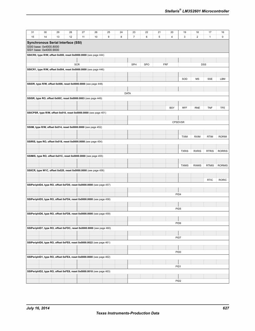
16171819202122232425262728293031
0123456789101112131415
Synchronous Serial Interface (SSI)SSI0 base: 0x4000.8000SSI1 base: 0x4000.9000
SSICR0, type R/W, offset 0x000, reset 0x0000.0000 (see page 444)
DSSFRFSPOSPHSCR
SSICR1, type R/W, offset 0x004, reset 0x0000.0000 (see page 446)
LBMSSEMSSOD
SSIDR, type R/W, offset 0x008, reset 0x0000.0000 (see page 448)
DATA
SSISR, type RO, offset 0x00C, reset 0x0000.0003 (see page 449)
TFETNFRNERFFBSY
SSICPSR, type R/W, offset 0x010, reset 0x0000.0000 (see page 451)
CPSDVSR
SSIIM, type R/W, offset 0x014, reset 0x0000.0000 (see page 452)
RORIMRTIMRXIMTXIM
SSIRIS, type RO, offset 0x018, reset 0x0000.0008 (see page 454)
RORRISRTRISRXRISTXRIS
SSIMIS, type RO, offset 0x01C, reset 0x0000.0000 (see page 455)
RORMISRTMISRXMISTXMIS
SSIICR, type W1C, offset 0x020, reset 0x0000.0000 (see page 456)
RORICRTIC
SSIPeriphID4, type RO, offset 0xFD0, reset 0x0000.0000 (see page 457)
PID4
SSIPeriphID5, type RO, offset 0xFD4, reset 0x0000.0000 (see page 458)
PID5
SSIPeriphID6, type RO, offset 0xFD8, reset 0x0000.0000 (see page 459)
PID6
SSIPeriphID7, type RO, offset 0xFDC, reset 0x0000.0000 (see page 460)
PID7
SSIPeriphID0, type RO, offset 0xFE0, reset 0x0000.0022 (see page 461)
PID0
SSIPeriphID1, type RO, offset 0xFE4, reset 0x0000.0000 (see page 462)
PID1
SSIPeriphID2, type RO, offset 0xFE8, reset 0x0000.0018 (see page 463)
PID2
627July 16, 2014Texas Instruments-Production Data
Stellaris® LM3S2601 Microcontroller
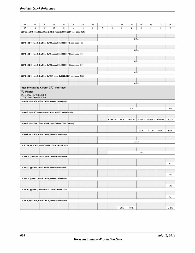
16171819202122232425262728293031
0123456789101112131415
SSIPeriphID3, type RO, offset 0xFEC, reset 0x0000.0001 (see page 464)
PID3
SSIPCellID0, type RO, offset 0xFF0, reset 0x0000.000D (see page 465)
CID0
SSIPCellID1, type RO, offset 0xFF4, reset 0x0000.00F0 (see page 466)
CID1
SSIPCellID2, type RO, offset 0xFF8, reset 0x0000.0005 (see page 467)
CID2
SSIPCellID3, type RO, offset 0xFFC, reset 0x0000.00B1 (see page 468)
CID3
Inter-Integrated Circuit (I2C) InterfaceI2C MasterI2C 0 base: 0x4002.0000I2C 1 base: 0x4002.1000
I2CMSA, type R/W, offset 0x000, reset 0x0000.0000
R/SSA
I2CMCS, type RO, offset 0x004, reset 0x0000.0000 (Reads)
BUSYERRORADRACKDATACKARBLSTIDLEBUSBSY
I2CMCS, type WO, offset 0x004, reset 0x0000.0000 (Writes)
RUNSTARTSTOPACK
I2CMDR, type R/W, offset 0x008, reset 0x0000.0000
DATA
I2CMTPR, type R/W, offset 0x00C, reset 0x0000.0001
TPR
I2CMIMR, type R/W, offset 0x010, reset 0x0000.0000
IM
I2CMRIS, type RO, offset 0x014, reset 0x0000.0000
RIS
I2CMMIS, type RO, offset 0x018, reset 0x0000.0000
MIS
I2CMICR, type WO, offset 0x01C, reset 0x0000.0000
IC
I2CMCR, type R/W, offset 0x020, reset 0x0000.0000
LPBKMFESFE
July 16, 2014628Texas Instruments-Production Data
Register Quick Reference
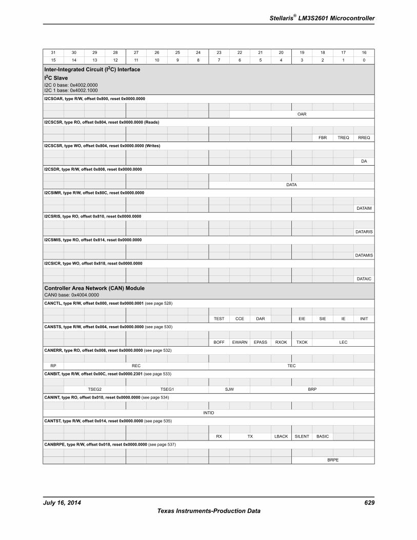
16171819202122232425262728293031
0123456789101112131415
Inter-Integrated Circuit (I2C) InterfaceI2C SlaveI2C 0 base: 0x4002.0000I2C 1 base: 0x4002.1000
I2CSOAR, type R/W, offset 0x800, reset 0x0000.0000
OAR
I2CSCSR, type RO, offset 0x804, reset 0x0000.0000 (Reads)
RREQTREQFBR
I2CSCSR, type WO, offset 0x804, reset 0x0000.0000 (Writes)
DA
I2CSDR, type R/W, offset 0x808, reset 0x0000.0000
DATA
I2CSIMR, type R/W, offset 0x80C, reset 0x0000.0000
DATAIM
I2CSRIS, type RO, offset 0x810, reset 0x0000.0000
DATARIS
I2CSMIS, type RO, offset 0x814, reset 0x0000.0000
DATAMIS
I2CSICR, type WO, offset 0x818, reset 0x0000.0000
DATAIC
Controller Area Network (CAN) ModuleCAN0 base: 0x4004.0000
CANCTL, type R/W, offset 0x000, reset 0x0000.0001 (see page 528)
INITIESIEEIEDARCCETEST
CANSTS, type R/W, offset 0x004, reset 0x0000.0000 (see page 530)
LECTXOKRXOKEPASSEWARNBOFF
CANERR, type RO, offset 0x008, reset 0x0000.0000 (see page 532)
TECRECRP
CANBIT, type R/W, offset 0x00C, reset 0x0000.2301 (see page 533)
BRPSJWTSEG1TSEG2
CANINT, type RO, offset 0x010, reset 0x0000.0000 (see page 534)
INTID
CANTST, type R/W, offset 0x014, reset 0x0000.0000 (see page 535)
BASICSILENTLBACKTXRX
CANBRPE, type R/W, offset 0x018, reset 0x0000.0000 (see page 537)
BRPE
629July 16, 2014Texas Instruments-Production Data
Stellaris® LM3S2601 Microcontroller
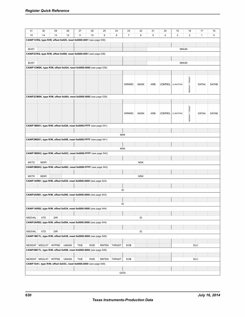
16171819202122232425262728293031
0123456789101112131415
CANIF1CRQ, type R/W, offset 0x020, reset 0x0000.0001 (see page 538)
MNUMBUSY
CANIF2CRQ, type R/W, offset 0x080, reset 0x0000.0001 (see page 538)
MNUMBUSY
CANIF1CMSK, type R/W, offset 0x024, reset 0x0000.0000 (see page 539)
DATABDATAA
NEWDAT
/TXRQST
CLRINTPNDCONTROLARBMASKWRNRD
CANIF2CMSK, type R/W, offset 0x084, reset 0x0000.0000 (see page 539)
DATABDATAA
NEWDAT
/TXRQST
CLRINTPNDCONTROLARBMASKWRNRD
CANIF1MSK1, type R/W, offset 0x028, reset 0x0000.FFFF (see page 541)
MSK
CANIF2MSK1, type R/W, offset 0x088, reset 0x0000.FFFF (see page 541)
MSK
CANIF1MSK2, type R/W, offset 0x02C, reset 0x0000.FFFF (see page 542)
MSKMDIRMXTD
CANIF2MSK2, type R/W, offset 0x08C, reset 0x0000.FFFF (see page 542)
MSKMDIRMXTD
CANIF1ARB1, type R/W, offset 0x030, reset 0x0000.0000 (see page 543)
ID
CANIF2ARB1, type R/W, offset 0x090, reset 0x0000.0000 (see page 543)
ID
CANIF1ARB2, type R/W, offset 0x034, reset 0x0000.0000 (see page 544)
IDDIRXTDMSGVAL
CANIF2ARB2, type R/W, offset 0x094, reset 0x0000.0000 (see page 544)
IDDIRXTDMSGVAL
CANIF1MCTL, type R/W, offset 0x038, reset 0x0000.0000 (see page 546)
DLCEOBTXRQSTRMTENRXIETXIEUMASKINTPNDMSGLSTNEWDAT
CANIF2MCTL, type R/W, offset 0x098, reset 0x0000.0000 (see page 546)
DLCEOBTXRQSTRMTENRXIETXIEUMASKINTPNDMSGLSTNEWDAT
CANIF1DA1, type R/W, offset 0x03C, reset 0x0000.0000 (see page 548)
DATA
July 16, 2014630Texas Instruments-Production Data
Register Quick Reference
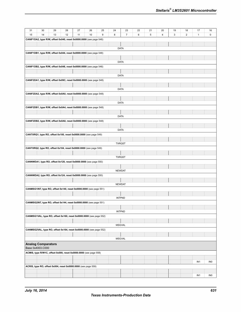
16171819202122232425262728293031
0123456789101112131415
CANIF1DA2, type R/W, offset 0x040, reset 0x0000.0000 (see page 548)
DATA
CANIF1DB1, type R/W, offset 0x044, reset 0x0000.0000 (see page 548)
DATA
CANIF1DB2, type R/W, offset 0x048, reset 0x0000.0000 (see page 548)
DATA
CANIF2DA1, type R/W, offset 0x09C, reset 0x0000.0000 (see page 548)
DATA
CANIF2DA2, type R/W, offset 0x0A0, reset 0x0000.0000 (see page 548)
DATA
CANIF2DB1, type R/W, offset 0x0A4, reset 0x0000.0000 (see page 548)
DATA
CANIF2DB2, type R/W, offset 0x0A8, reset 0x0000.0000 (see page 548)
DATA
CANTXRQ1, type RO, offset 0x100, reset 0x0000.0000 (see page 549)
TXRQST
CANTXRQ2, type RO, offset 0x104, reset 0x0000.0000 (see page 549)
TXRQST
CANNWDA1, type RO, offset 0x120, reset 0x0000.0000 (see page 550)
NEWDAT
CANNWDA2, type RO, offset 0x124, reset 0x0000.0000 (see page 550)
NEWDAT
CANMSG1INT, type RO, offset 0x140, reset 0x0000.0000 (see page 551)
INTPND
CANMSG2INT, type RO, offset 0x144, reset 0x0000.0000 (see page 551)
INTPND
CANMSG1VAL, type RO, offset 0x160, reset 0x0000.0000 (see page 552)
MSGVAL
CANMSG2VAL, type RO, offset 0x164, reset 0x0000.0000 (see page 552)
MSGVAL
Analog ComparatorsBase 0x4003.C000
ACMIS, type R/W1C, offset 0x000, reset 0x0000.0000 (see page 558)
IN0IN1
ACRIS, type RO, offset 0x004, reset 0x0000.0000 (see page 559)
IN0IN1
631July 16, 2014Texas Instruments-Production Data
Stellaris® LM3S2601 Microcontroller
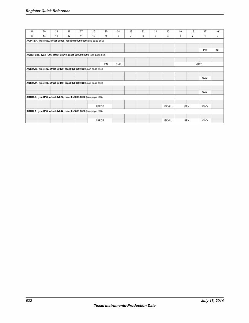
16171819202122232425262728293031
0123456789101112131415
ACINTEN, type R/W, offset 0x008, reset 0x0000.0000 (see page 560)
IN0IN1
ACREFCTL, type R/W, offset 0x010, reset 0x0000.0000 (see page 561)
VREFRNGEN
ACSTAT0, type RO, offset 0x020, reset 0x0000.0000 (see page 562)
OVAL
ACSTAT1, type RO, offset 0x040, reset 0x0000.0000 (see page 562)
OVAL
ACCTL0, type R/W, offset 0x024, reset 0x0000.0000 (see page 563)
CINVISENISLVALASRCP
ACCTL1, type R/W, offset 0x044, reset 0x0000.0000 (see page 563)
CINVISENISLVALASRCP
July 16, 2014632Texas Instruments-Production Data
Register Quick Reference
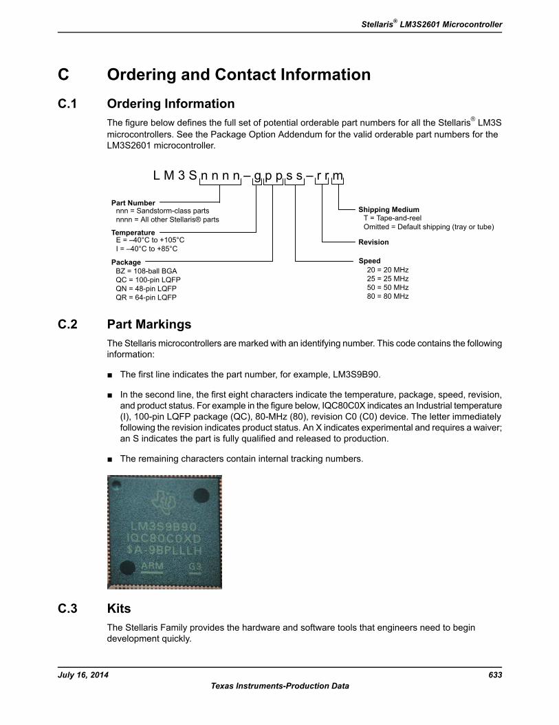
C Ordering and Contact InformationC.1 Ordering Information
The figure below defines the full set of potential orderable part numbers for all the Stellaris® LM3Smicrocontrollers. See the Package Option Addendum for the valid orderable part numbers for theLM3S2601 microcontroller.
L M 3 S n n n n – g p p s s – r r m
Part Number
Temperature
Package Speed
Revision
Shipping Medium
E = –40°C to +105°CI = –40°C to +85°C
T = Tape-and-reelOmitted = Default shipping (tray or tube)
BZ = 108-ball BGAQC = 100-pin LQFPQN = 48-pin LQFPQR = 64-pin LQFP
20 = 20 MHz25 = 25 MHz50 = 50 MHz80 = 80 MHz
nnn = Sandstorm-class partsnnnn = All other Stellaris® parts
C.2 Part MarkingsThe Stellaris microcontrollers are marked with an identifying number. This code contains the followinginformation:
The first line indicates the part number, for example, LM3S9B90.
In the second line, the first eight characters indicate the temperature, package, speed, revision,and product status. For example in the figure below, IQC80C0X indicates an Industrial temperature(I), 100-pin LQFP package (QC), 80-MHz (80), revision C0 (C0) device. The letter immediatelyfollowing the revision indicates product status. An X indicates experimental and requires a waiver;an S indicates the part is fully qualified and released to production.
The remaining characters contain internal tracking numbers.
C.3 KitsThe Stellaris Family provides the hardware and software tools that engineers need to begindevelopment quickly.
633July 16, 2014Texas Instruments-Production Data
Stellaris® LM3S2601 Microcontroller
Reference Design Kits accelerate product development by providing ready-to-run hardware andcomprehensive documentation including hardware design files
Evaluation Kits provide a low-cost and effective means of evaluating Stellaris microcontrollersbefore purchase
Development Kits provide you with all the tools you need to develop and prototype embeddedapplications right out of the box
See the website at www.ti.com/stellaris for the latest tools available, or ask your distributor.
C.4 Support InformationFor support on Stellaris products, contact the TI Worldwide Product Information Center nearest you:http://www-k.ext.ti.com/sc/technical-support/product-information-centers.htm.
July 16, 2014634Texas Instruments-Production Data
Ordering and Contact Information
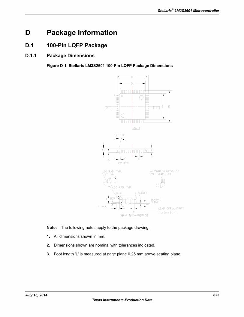
D Package InformationD.1 100-Pin LQFP Package
D.1.1 Package Dimensions
Figure D-1. Stellaris LM3S2601 100-Pin LQFP Package Dimensions
Note: The following notes apply to the package drawing.
1. All dimensions shown in mm.
2. Dimensions shown are nominal with tolerances indicated.
3. Foot length 'L' is measured at gage plane 0.25 mm above seating plane.
635July 16, 2014Texas Instruments-Production Data
Stellaris® LM3S2601 Microcontroller
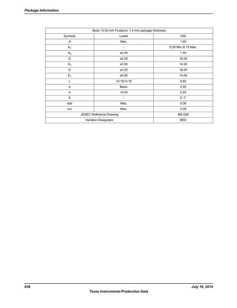
Body +2.00 mm Footprint, 1.4 mm package thickness
100LLeadsSymbols
1.60Max.A
0.05 Min./0.15 Max.-A11.40±0.05A216.00±0.20D
14.00±0.05D1
16.00±0.20E
14.00±0.05E10.60+0.15/-0.10L
0.50Basice
0.22+0.05b
0˚-7˚-θ
0.08Max.ddd
0.08Max.ccc
MS-026JEDEC Reference Drawing
BEDVariation Designator
July 16, 2014636Texas Instruments-Production Data
Package Information
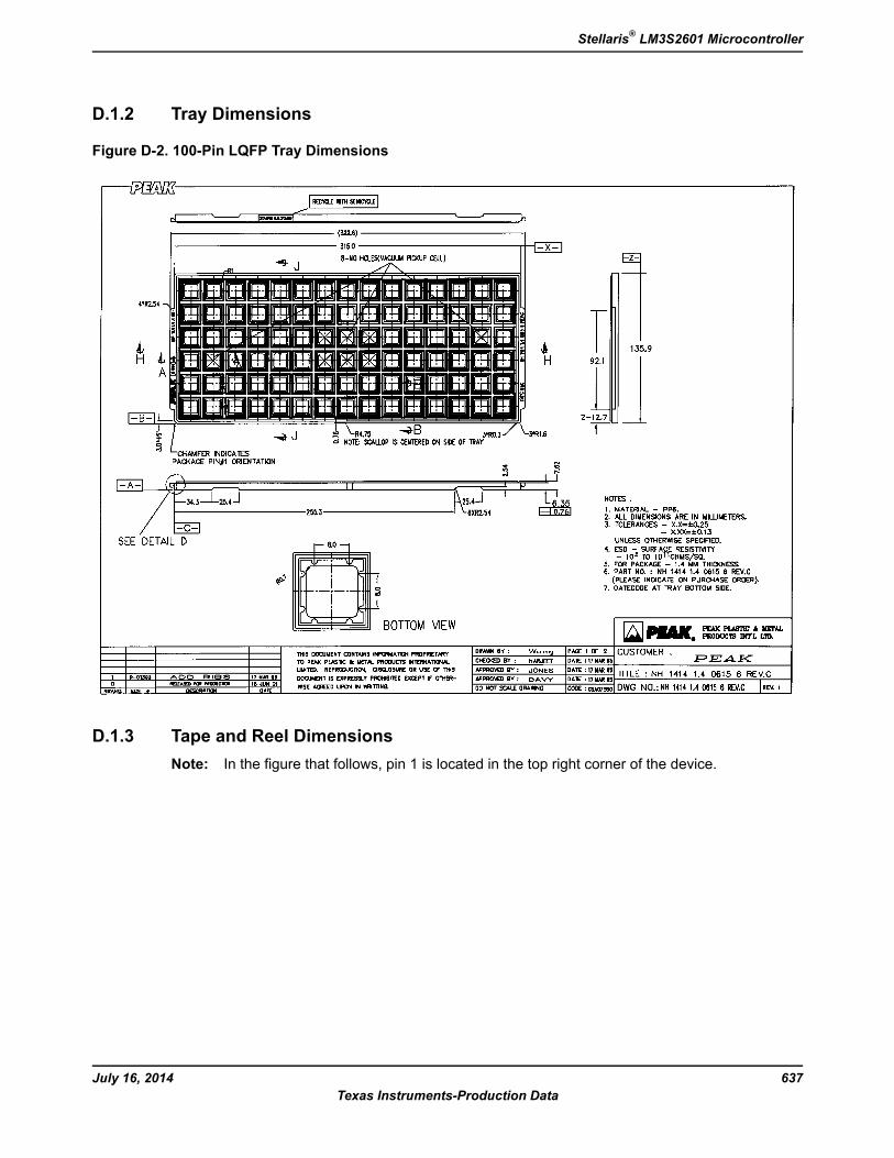
D.1.2 Tray Dimensions
Figure D-2. 100-Pin LQFP Tray Dimensions
D.1.3 Tape and Reel DimensionsNote: In the figure that follows, pin 1 is located in the top right corner of the device.
637July 16, 2014Texas Instruments-Production Data
Stellaris® LM3S2601 Microcontroller
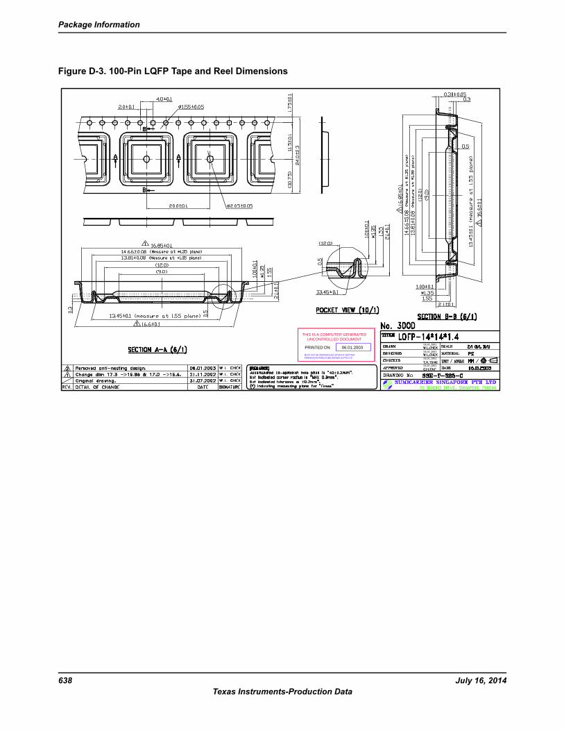
Figure D-3. 100-Pin LQFP Tape and Reel Dimensions
PRINTED ON
MUST NOT BE REPRODUCED WITHOUT WRITTEN PERMISSION FROM SUMICARRIER (S) PTE LTD
06.01.2003
THIS IS A COMPUTER GENERATED UNCONTROLLED DOCUMENT
06.01.2003
06.01.2003
06.01.2003
06.01.2003
July 16, 2014638Texas Instruments-Production Data
Package Information
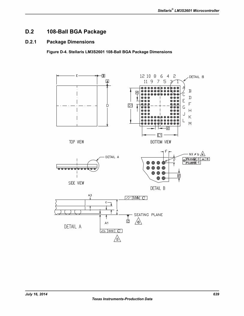
D.2 108-Ball BGA Package
D.2.1 Package Dimensions
Figure D-4. Stellaris LM3S2601 108-Ball BGA Package Dimensions
639July 16, 2014Texas Instruments-Production Data
Stellaris® LM3S2601 Microcontroller
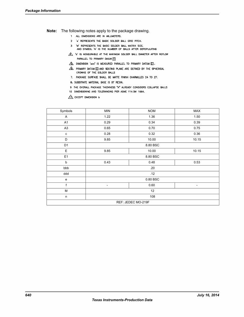
Note: The following notes apply to the package drawing.
MAXNOMMINSymbols
1.501.361.22A
0.390.340.29A1
0.750.700.65A3
0.360.320.28c
10.1510.009.85D
8.80 BSCD1
10.1510.009.85E
8.80 BSCE1
0.530.480.43b
.20bbb
.12ddd
0.80 BSCe
-0.60-f
12M
108n
REF: JEDEC MO-219F
July 16, 2014640Texas Instruments-Production Data
Package Information
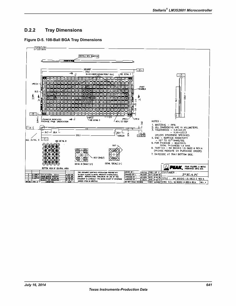
D.2.2 Tray Dimensions
Figure D-5. 108-Ball BGA Tray Dimensions
641July 16, 2014Texas Instruments-Production Data
Stellaris® LM3S2601 Microcontroller
D.2.3 Tape and Reel Dimensions
Figure D-6. 108-Ball BGA Tape and Reel Dimensions
C-PAK PTE LTD
July 16, 2014642Texas Instruments-Production Data
Package Information

IMPORTANT NOTICE AND DISCLAIMERTI PROVIDES TECHNICAL AND RELIABILITY DATA (INCLUDING DATASHEETS), DESIGN RESOURCES (INCLUDING REFERENCEDESIGNS), APPLICATION OR OTHER DESIGN ADVICE, WEB TOOLS, SAFETY INFORMATION, AND OTHER RESOURCES “AS IS”AND WITH ALL FAULTS, AND DISCLAIMS ALL WARRANTIES, EXPRESS AND IMPLIED, INCLUDING WITHOUT LIMITATION ANYIMPLIED WARRANTIES OF MERCHANTABILITY, FITNESS FOR A PARTICULAR PURPOSE OR NON-INFRINGEMENT OF THIRDPARTY INTELLECTUAL PROPERTY RIGHTS.These resources are intended for skilled developers designing with TI products. You are solely responsible for (1) selecting the appropriateTI products for your application, (2) designing, validating and testing your application, and (3) ensuring your application meets applicablestandards, and any other safety, security, or other requirements. These resources are subject to change without notice. TI grants youpermission to use these resources only for development of an application that uses the TI products described in the resource. Otherreproduction and display of these resources is prohibited. No license is granted to any other TI intellectual property right or to any third partyintellectual property right. TI disclaims responsibility for, and you will fully indemnify TI and its representatives against, any claims, damages,costs, losses, and liabilities arising out of your use of these resources.TI’s products are provided subject to TI’s Terms of Sale (https:www.ti.com/legal/termsofsale.html) or other applicable terms available eitheron ti.com or provided in conjunction with such TI products. TI’s provision of these resources does not expand or otherwise alter TI’sapplicable warranties or warranty disclaimers for TI products.IMPORTANT NOTICE
Mailing Address: Texas Instruments, Post Office Box 655303, Dallas, Texas 75265Copyright © 2021, Texas Instruments Incorporated