Embed Size (px)
Citation preview
8/8/2019 Pcie Basics Pcisig
http://slidepdf.com/reader/full/pcie-basics-pcisig 1/40
Copyright © 2007, PCI-SIG, All Rights Reserved 1
PCI Express ® Basics
Ravi Budruk
Senior Staff Engineer and Partner
MindShare, Inc.
Ravi Budruk
Senior Staff Engineer and Partner
MindShare, Inc.
8/8/2019 Pcie Basics Pcisig
http://slidepdf.com/reader/full/pcie-basics-pcisig 2/40
Copyright © 2007, PCI-SIG, All Rights Reserved 2PCI-SIG Developers Conference
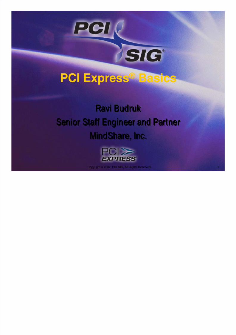
PCI Express architecture is a high performance, IOinterconnect for peripherals incomputing/communication platforms
Evolved from PCI and PCI-X™ architectures Yet PCI Express architecture is significantly different from its
predecessors PCI and PCI-X
PCI Express is a serial point-to-point interconnectbetween two devices
Implements packet based protocol for informationtransfer
Scalable performance based on number of signalLanes implemented on the PCI Express interconnect
PCI Express Introduction
8/8/2019 Pcie Basics Pcisig
http://slidepdf.com/reader/full/pcie-basics-pcisig 3/40
Copyright © 2007, PCI-SIG, All Rights Reserved 3PCI-SIG Developers Conference
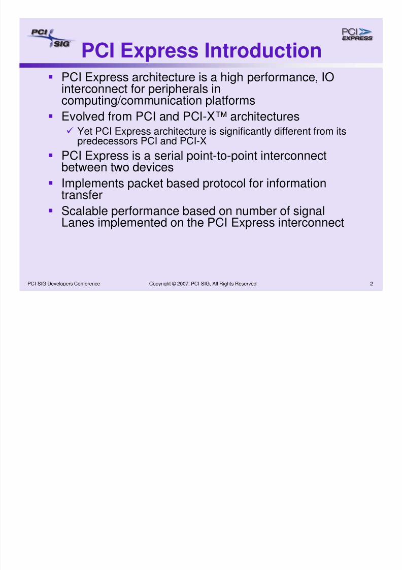
Link
Lane
PCI Express Terminology
PCI Express Device A
PCI Express Device B
Signal
Wire
8/8/2019 Pcie Basics Pcisig
http://slidepdf.com/reader/full/pcie-basics-pcisig 4/40
Copyright © 2007, PCI-SIG, All Rights Reserved 4PCI-SIG Developers Conference
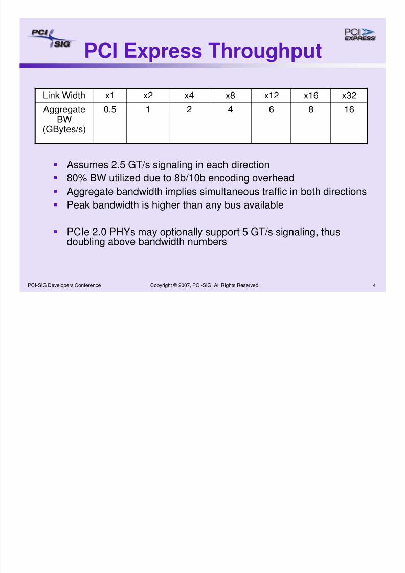
Assumes 2.5 GT/s signaling in each direction 80% BW utilized due to 8b/10b encoding overhead
Aggregate bandwidth implies simultaneous traffic in both directions
Peak bandwidth is higher than any bus available
PCIe 2.0 PHYs may optionally support 5 GT/s signaling, thusdoubling above bandwidth numbers
16864210.5AggregateBW
(GBytes/s)
x32x16x12x8x4x2x1Link Width
PCI Express Throughput
8/8/2019 Pcie Basics Pcisig
http://slidepdf.com/reader/full/pcie-basics-pcisig 5/40
Copyright © 2007, PCI-SIG, All Rights Reserved 5PCI-SIG Developers Conference
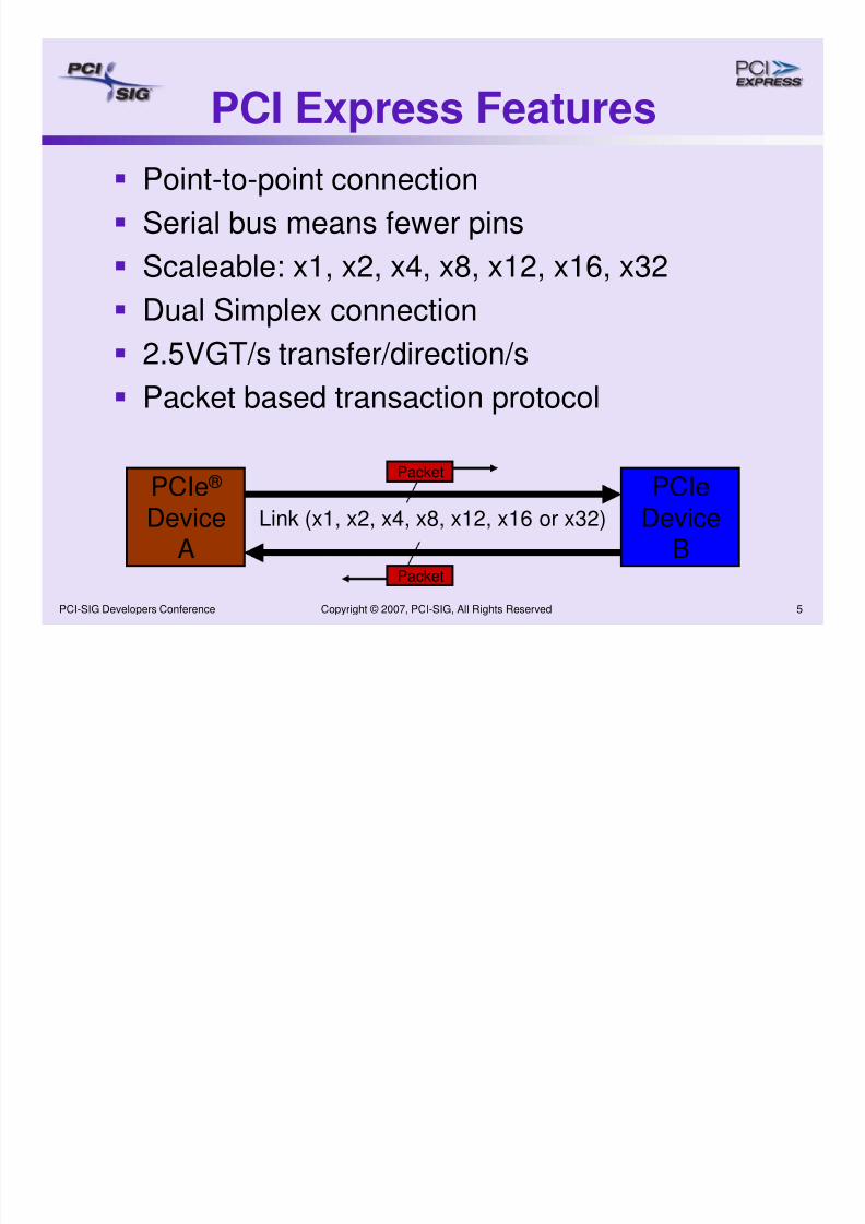
PCI Express Features Point-to-point connection
Serial bus means fewer pins
Scaleable: x1, x2, x4, x8, x12, x16, x32
Dual Simplex connection
2.5VGT/s transfer/direction/s Packet based transaction protocol
PCIe ®
DeviceA
PCIeDevice
B
Link (x1, x2, x4, x8, x12, x16 or x32)
Packet
Packet
8/8/2019 Pcie Basics Pcisig
http://slidepdf.com/reader/full/pcie-basics-pcisig 6/40
Copyright © 2007, PCI-SIG, All Rights Reserved 6PCI-SIG Developers Conference
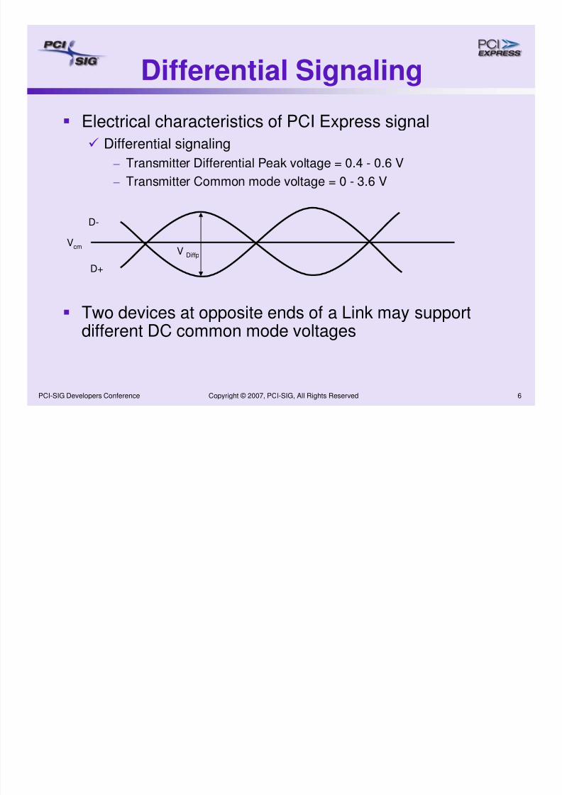
Electrical characteristics of PCI Express signal
Differential signaling
– Transmitter Differential Peak voltage = 0.4 - 0.6 V
– Transmitter Common mode voltage = 0 - 3.6 V
Two devices at opposite ends of a Link may supportdifferent DC common mode voltages
D+
D-
V Diffp
Vcm
Differential Signaling
8/8/2019 Pcie Basics Pcisig
http://slidepdf.com/reader/full/pcie-basics-pcisig 7/40
Copyright © 2007, PCI-SIG, All Rights Reserved 7PCI-SIG Developers Conference
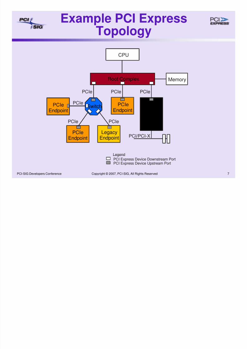
Switch
PCIeEndpoint
LegacyEndpoint
PCIeEndpoint
Root Complex
CPU
PCIe
Memory
PCIeBridge To
PCIe PCIe
PCIe PCIe
Legend
PCI Express Device Downstream PortPCI Express Device Upstream Port
PCIeEndpoint
PCI/PCI-X
PCI/PCI-X
Example PCI Express
Topology
PCIe
8/8/2019 Pcie Basics Pcisig
http://slidepdf.com/reader/full/pcie-basics-pcisig 8/40
Copyright © 2007, PCI-SIG, All Rights Reserved 8PCI-SIG Developers Conference
Switch
PCIeEndpoint LegacyEndpoint
PCIeEndpoint
Root Complex
CPU
PCIe
Memory
PCIeBridge To
PCIe PCIe
PCIe PCIe
Legend
PCI Express Device Downstream PortPCI Express Device Upstream Port
PCIeEndpoint
PCI/PCI-X
PCI/PCI-X
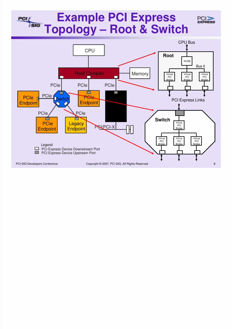
Root
VirtualPCI
Bridge
VirtualPCI
Bridge
VirtualPCI
Bridge
RCRB
Bus 0
PCI Express Links
CPU Bus
Switch
VirtualPCI
Bridge
VirtualPCI
Bridge
VirtualPCI
Bridge
Virtual
PCIBridge
Example PCI Express
Topology – Root & Switch
PCIe
8/8/2019 Pcie Basics Pcisig
http://slidepdf.com/reader/full/pcie-basics-pcisig 9/40
Copyright © 2007, PCI-SIG, All Rights Reserved 9PCI-SIG Developers Conference
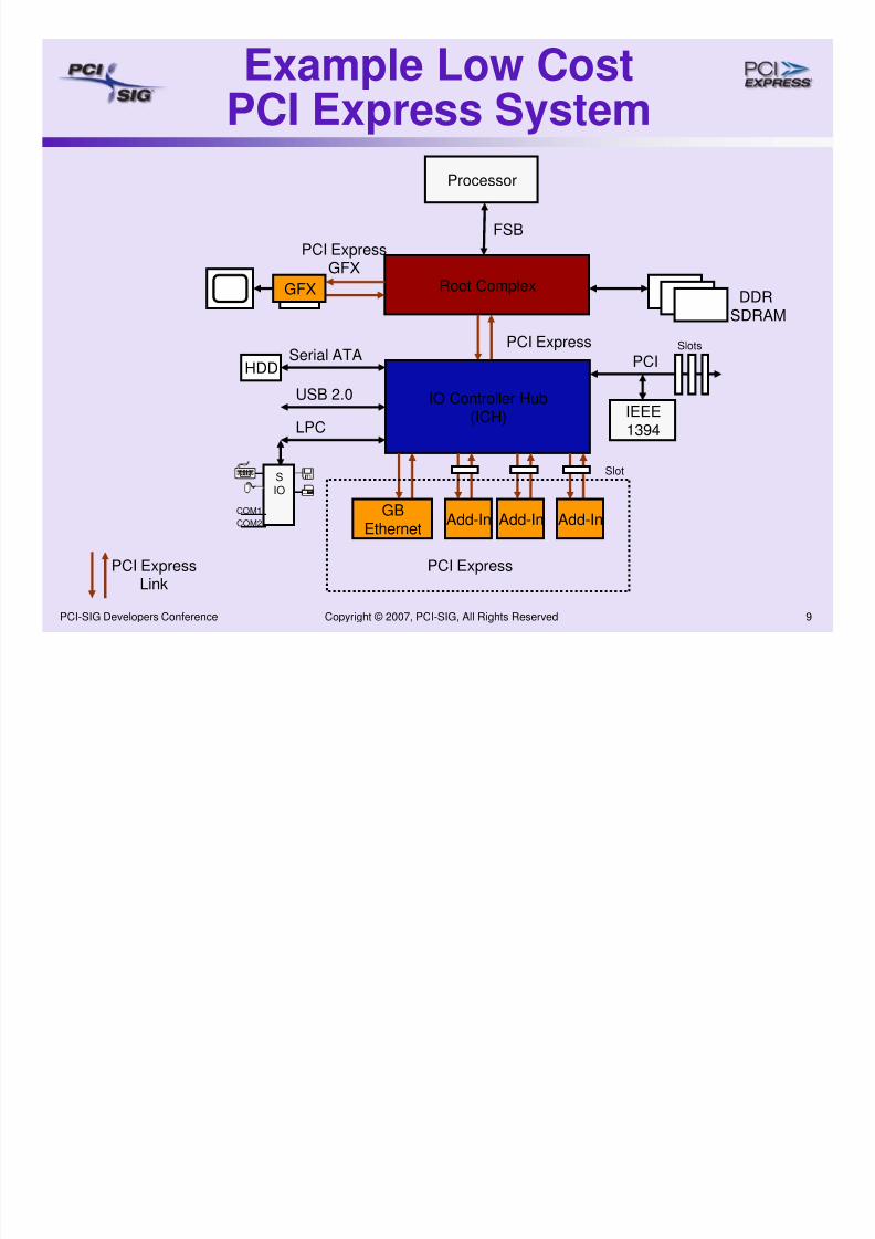
Processor
Root ComplexDDR
SDRAM
IO Controller Hub(ICH) IEEE
1394
PCI ExpressGFX
PCI
PCI Express
Serial ATAHDD
USB 2.0
LPC
GBEthernet
Add-In Add-In Add-In
PCI Express
GFX
FSB
PCI Express
Link
SIO
COM1
COM2
Slot
Slots
Example Low Cost
PCI Express System
8/8/2019 Pcie Basics Pcisig
http://slidepdf.com/reader/full/pcie-basics-pcisig 10/40
Copyright © 2007, PCI-SIG, All Rights Reserved 10PCI-SIG Developers Conference
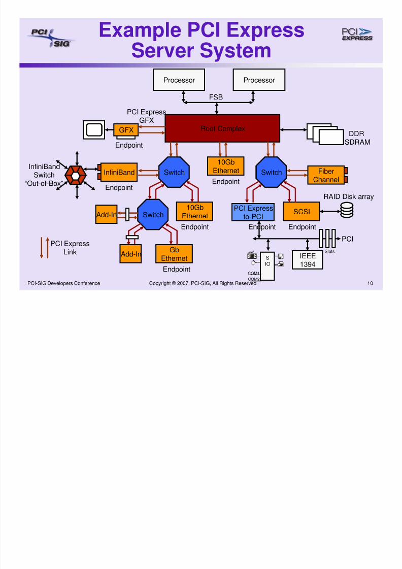
Processor Processor
Root ComplexGFXDDR
SDRAM
10Gb
Ethernet
PCI
InfiniBandSwitch
“Out-of-Box”
SCSI
RAID Disk array
IEEE1394
InfiniBand
GbEthernet
PCI ExpressLink
Switch Switch
Switch
PCI ExpressGFX
FSB
S
IO
COM1
COM2
Endpoint
Endpoint
Endpoint Endpoint
Endpoint
Endpoint
10GbEthernet
Endpoint
Add-In
Add-In
FiberChannel
Slots
PCI Express
to-PCI
Example PCI Express
Server System
8/8/2019 Pcie Basics Pcisig
http://slidepdf.com/reader/full/pcie-basics-pcisig 11/40
Copyright © 2007, PCI-SIG, All Rights Reserved 11PCI-SIG Developers Conference
Request are translated to one of four transaction types bythe Transaction Layer:
1. Memory Read or Memory Write. Used to transfer data from or to amemory mapped location
– The protocol also supports a locked memory read transaction variant.
2. I/O Read or I/O Write. Used to transfer data from or to an I/O location
– These transactions are restricted to supporting legacy endpointdevices.
3. Configuration Read or Configuration Write. Used to discover devicecapabilities, program features, and check status in the 4KB PCI Expressconfiguration space.
4. Messages. Handled like posted writes. Used for event signaling andgeneral purpose messaging.
Transaction Types,
Address Spaces
8/8/2019 Pcie Basics Pcisig
http://slidepdf.com/reader/full/pcie-basics-pcisig 12/40
Copyright © 2007, PCI-SIG, All Rights Reserved 12PCI-SIG Developers Conference
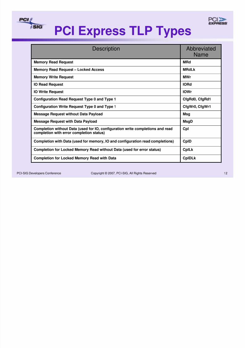
CplDCompletion with Data (used for memory, IO and configuration read completions)
CplCompletion without Data (used for IO, configuration write completions and read
completion with error completion status)
MRdMemory Read Request
CplDLk
CplLk
MsgD
Msg
CfgWr0, CfgWr1
CfgRd0, CfgRd1
IOWr
IORd
MWr
MRdLk
AbbreviatedName
Completion for Locked Memory Read with Data
Completion for Locked Memory Read without Data (used for error status)
Message Request with Data Payload
Message Request without Data Payload
Configuration Write Request Type 0 and Type 1
Configuration Read Request Type 0 and Type 1
IO Write Request
IO Read Request
Memory Write Request
Memory Read Request – Locked Access
Description
PCI Express TLP Types
8/8/2019 Pcie Basics Pcisig
http://slidepdf.com/reader/full/pcie-basics-pcisig 13/40
Copyright © 2007, PCI-SIG, All Rights Reserved 13PCI-SIG Developers Conference
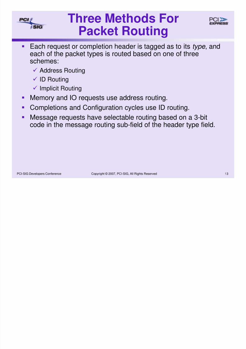
Each request or completion header is tagged as to its type , andeach of the packet types is routed based on one of threeschemes:
Address Routing
ID Routing
Implicit Routing
Memory and IO requests use address routing.
Completions and Configuration cycles use ID routing.
Message requests have selectable routing based on a 3-bitcode in the message routing sub-field of the header type field.
Three Methods For
Packet Routing
8/8/2019 Pcie Basics Pcisig
http://slidepdf.com/reader/full/pcie-basics-pcisig 14/40
Copyright © 2007, PCI-SIG, All Rights Reserved 14PCI-SIG Developers Conference
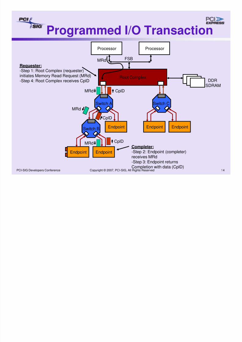
Programmed I/O TransactionProcessor Processor
Root ComplexDDR
SDRAM
Endpoint Endpoint Endpoint
Endpoint Endpoint
Switch A Switch C
Switch B
FSB
MRd
MRd
MRd CplD
CplD
CplD
Requester:-Step 1: Root Complex (requester)initiates Memory Read Request (MRd)-Step 4: Root Complex receives CplD
Completer:-Step 2: Endpoint (completer)receives MRd
-Step 3: Endpoint returnsCompletion with data (CplD)
MRd
8/8/2019 Pcie Basics Pcisig
http://slidepdf.com/reader/full/pcie-basics-pcisig 15/40
Copyright © 2007, PCI-SIG, All Rights Reserved 15PCI-SIG Developers Conference
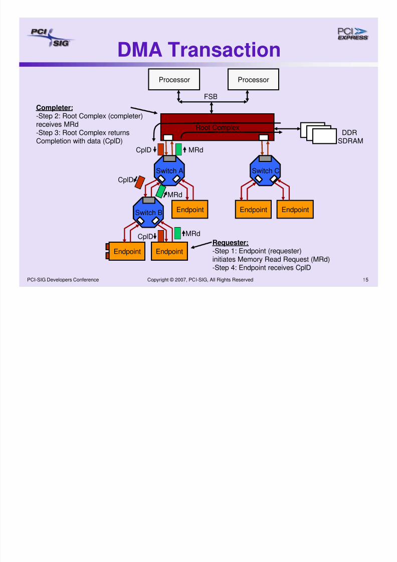
Processor Processor
Root ComplexDDR
SDRAM
Endpoint Endpoint Endpoint
Endpoint
Switch A Switch C
Switch B
FSB
Requester:-Step 1: Endpoint (requester)initiates Memory Read Request (MRd)
-Step 4: Endpoint receives CplD
MRd
MRd
MRd
Completer:-Step 2: Root Complex (completer)receives MRd-Step 3: Root Complex returnsCompletion with data (CplD)
CplD
CplD
CplD
Endpoint
DMA Transaction
8/8/2019 Pcie Basics Pcisig
http://slidepdf.com/reader/full/pcie-basics-pcisig 16/40
Copyright © 2007, PCI-SIG, All Rights Reserved 16PCI-SIG Developers Conference
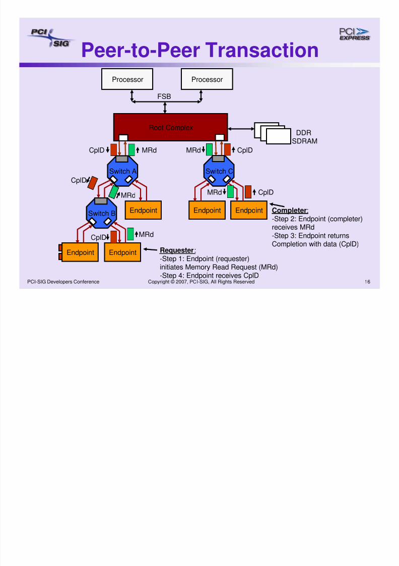
Processor Processor
Root ComplexDDR
SDRAM
Endpoint Endpoint Endpoint
Endpoint Endpoint
Switch A Switch C
Switch B
FSB
Requester:-Step 1: Endpoint (requester)initiates Memory Read Request (MRd)-Step 4: Endpoint receives CplD
MRd
MRd
MRd
Completer:
-Step 2: Endpoint (completer)receives MRd-Step 3: Endpoint returnsCompletion with data (CplD)
CplD
CplD
CplD MRd
MRd CplD
CplD
Peer-to-Peer Transaction
8/8/2019 Pcie Basics Pcisig
http://slidepdf.com/reader/full/pcie-basics-pcisig 17/40
Copyright © 2007, PCI-SIG, All Rights Reserved 17PCI-SIG Developers Conference
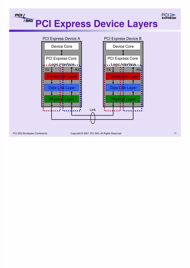
PCI Express Device Layers
Device Core
PCI Express Core
Logic Interface
Transaction Layer
Data Link Layer
Physical Layer
TX RX
PCI Express Device A
Device Core
PCI Express Core
Logic Interface
Transaction Layer
Data Link Layer
Physical Layer
TX RX
PCI Express Device B
Link
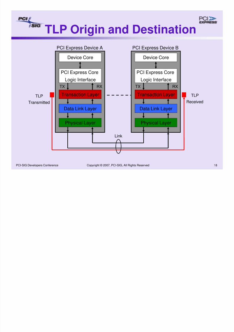
8/8/2019 Pcie Basics Pcisig
http://slidepdf.com/reader/full/pcie-basics-pcisig 18/40
Copyright © 2007, PCI-SIG, All Rights Reserved 18PCI-SIG Developers Conference
Device Core
PCI Express Core
Logic Interface
Transaction Layer
Data Link Layer
Physical Layer
TX RX
PCI Express Device A
Device Core
PCI Express Core
Logic Interface
Transaction Layer
Data Link Layer
Physical Layer
TX RX
PCI Express Device B
Link
TLPTransmitted
TLPReceived
TLP Origin and Destination
8/8/2019 Pcie Basics Pcisig
http://slidepdf.com/reader/full/pcie-basics-pcisig 19/40
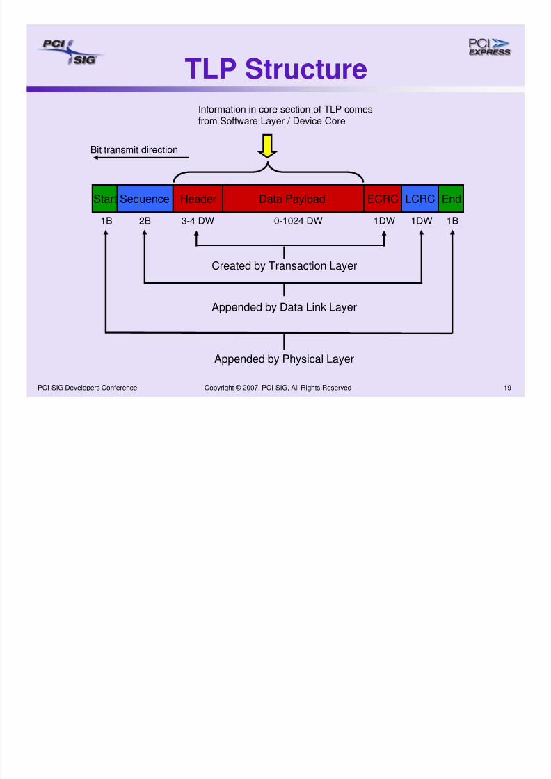
Copyright © 2007, PCI-SIG, All Rights Reserved 19PCI-SIG Developers Conference
Created by Transaction Layer
Appended by Data Link Layer
Appended by Physical Layer
Bit transmit direction
Information in core section of TLP comesfrom Software Layer / Device Core
TLP Structure
Header Data Payload ECRCSequence LCRCStart End
1B 2B 1DW 1B1DW0-1024 DW3-4 DW
8/8/2019 Pcie Basics Pcisig
http://slidepdf.com/reader/full/pcie-basics-pcisig 20/40
Copyright © 2007, PCI-SIG, All Rights Reserved 20PCI-SIG Developers Conference
Device Core
PCI Express Core
Logic Interface
Transaction Layer
Data Link Layer
Physical Layer
TX RX
PCI Express Device A
Device Core
PCI Express Core
Logic Interface
Transaction Layer
Data Link Layer
Physical Layer
TX RX
PCI Express Device B
Link
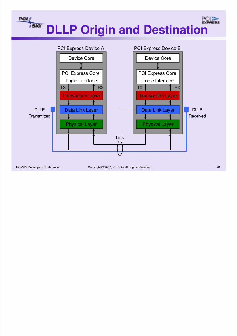
DLLP
Transmitted
DLLP
Received
DLLP Origin and Destination
8/8/2019 Pcie Basics Pcisig
http://slidepdf.com/reader/full/pcie-basics-pcisig 21/40
Copyright © 2007, PCI-SIG, All Rights Reserved 21PCI-SIG Developers Conference
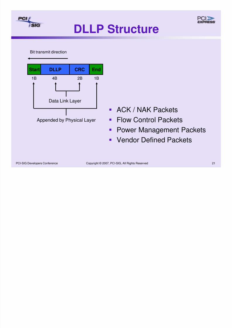
Start EndDLLP CRC
Data Link Layer
Appended by Physical Layer
Bit transmit direction
DLLP Structure
ACK / NAK Packets
Flow Control Packets
Power Management Packets
Vendor Defined Packets
1B 4B 2B 1B
8/8/2019 Pcie Basics Pcisig
http://slidepdf.com/reader/full/pcie-basics-pcisig 22/40
Copyright © 2007, PCI-SIG, All Rights Reserved 22PCI-SIG Developers Conference
Device Core
PCI Express Core
Logic Interface
Transaction Layer
Data Link Layer
Physical Layer
TX RX
PCI Express Device A
Device Core
PCI Express Core
Logic Interface
Transaction Layer
Data Link Layer
Physical Layer
TX RX
PCI Express Device B
Link
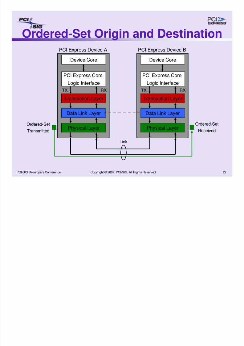
Ordered-Set
Transmitted
Ordered-Set
Received
Ordered-Set Origin and Destination
8/8/2019 Pcie Basics Pcisig
http://slidepdf.com/reader/full/pcie-basics-pcisig 23/40
Copyright © 2007, PCI-SIG, All Rights Reserved 23PCI-SIG Developers Conference
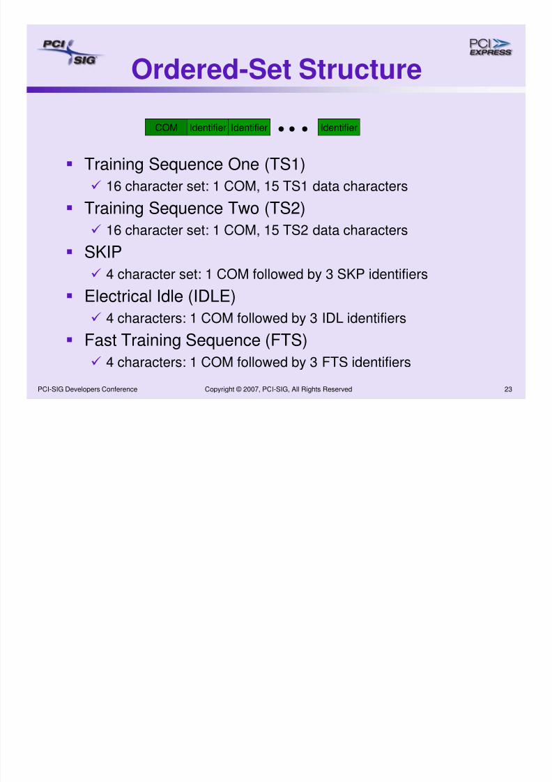
COM Identifier Identifier Identifier
Training Sequence One (TS1)
16 character set: 1 COM, 15 TS1 data characters
Training Sequence Two (TS2)
16 character set: 1 COM, 15 TS2 data characters
SKIP
4 character set: 1 COM followed by 3 SKP identifiers
Electrical Idle (IDLE) 4 characters: 1 COM followed by 3 IDL identifiers
Fast Training Sequence (FTS)
4 characters: 1 COM followed by 3 FTS identifiers
Ordered-Set Structure
8/8/2019 Pcie Basics Pcisig
http://slidepdf.com/reader/full/pcie-basics-pcisig 24/40
Copyright © 2007, PCI-SIG, All Rights Reserved 24PCI-SIG Developers Conference
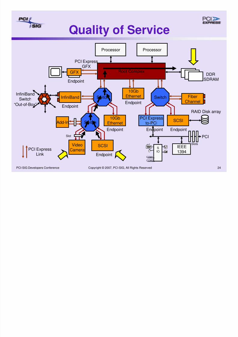
Processor Processor
Root ComplexGFXDDR
SDRAM
10GbEthernet
PCI Expressto-PCI
PCI
InfiniBand
Switch
SCSI
RAID Disk array
IEEE1394
“Out-of-Box”InfiniBand
SCSIPCI Express
Link
Switch Switch
Switch
PCI Express
GFX
SIO
COM1
COM2
Endpoint
Endpoint
Endpoint Endpoint
Endpoint
Endpoint
10Gb
EthernetEndpoint
Add-In
VideoCamera
FiberChannel
Slots
Slot
Quality of Service
8/8/2019 Pcie Basics Pcisig
http://slidepdf.com/reader/full/pcie-basics-pcisig 25/40
Copyright © 2007, PCI-SIG, All Rights Reserved 25PCI-SIG Developers Conference
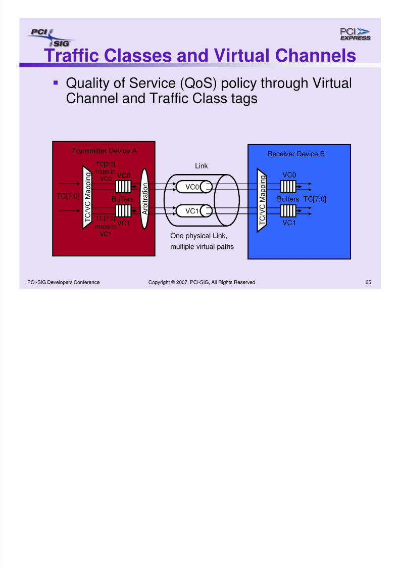
Receiver Device B
Quality of Service (QoS) policy through VirtualChannel and Traffic Class tags
VC0
VC1
T C / V C
M a p p i n g
TC[7:0]
TC[2:0]maps to
VC0
TC[7:3]maps to
VC1
Transmitter Device A
Link
Buffers
A r b i t r a t i o n
Buffers TC[7:0]
VC0
VC1
VC0
VC1
One physical Link,
multiple virtual paths
T C
/ V C
M a p p i n g
Traffic Classes and Virtual Channels
8/8/2019 Pcie Basics Pcisig
http://slidepdf.com/reader/full/pcie-basics-pcisig 26/40
Copyright © 2007, PCI-SIG, All Rights Reserved 26PCI-SIG Developers Conference
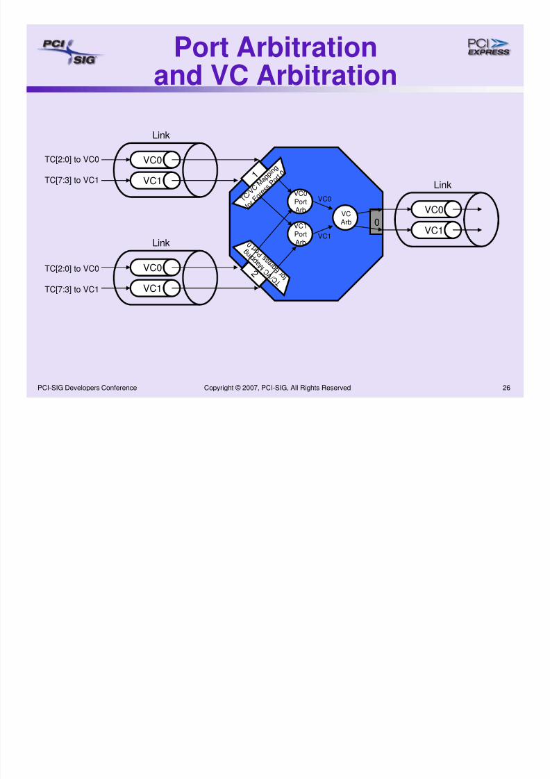
VC0
0
1
2
VC1
TC[2:0] to VC0
TC[7:3] to VC1
Link
T C / V C M a p p i n g
f o r E g r e s s P o r t 0
VC0
VC1
TC[2:0] to VC0
TC[7:3] to VC1
Link
VC0
PortArb
VC1PortArb
VCArb
VC0
VC1
Link
T C / V C M a
p p i n g
f o r E g r e s
s P o r t 0
VC0
VC1
Port Arbitration
and VC Arbitration
8/8/2019 Pcie Basics Pcisig
http://slidepdf.com/reader/full/pcie-basics-pcisig 27/40
Copyright © 2007, PCI-SIG, All Rights Reserved 27PCI-SIG Developers Conference
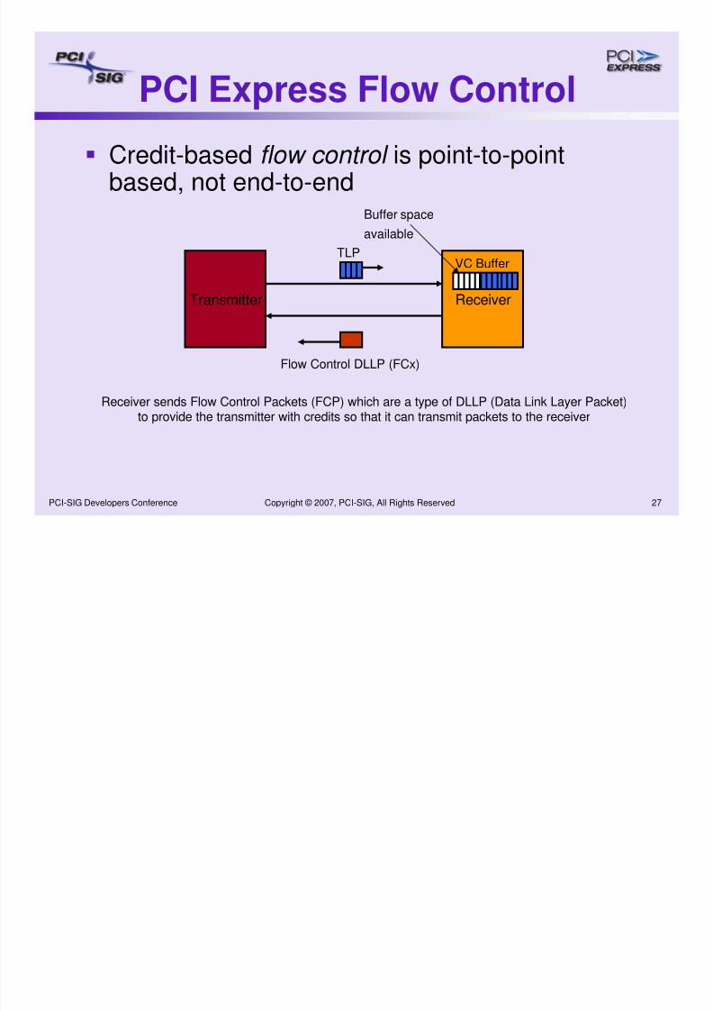
Credit-based flow control is point-to-pointbased, not end-to-end
ReceiverTransmitter
Flow Control DLLP (FCx)
TLPVC Buffer
Receiver sends Flow Control Packets (FCP) which are a type of DLLP (Data Link Layer Packet)to provide the transmitter with credits so that it can transmit packets to the receiver
Buffer space
available
PCI Express Flow Control
8/8/2019 Pcie Basics Pcisig
http://slidepdf.com/reader/full/pcie-basics-pcisig 28/40
Copyright © 2007, PCI-SIG, All Rights Reserved 28PCI-SIG Developers Conference
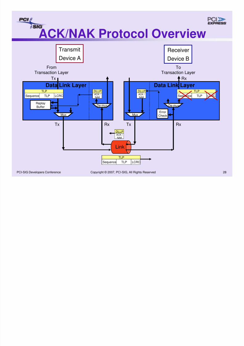
ReplayBuffer
ACK / NAK
DLLP
De-mux
Mux
FromTransaction Layer
Data Link Layer
Tx Rx
TLP
Sequence TLP LCRC
Transmit
Device A
Receiver
Device B
Tx
ErrorCheck
TLP
Sequence TLP LCRC
De-mux
Mux
ToTransaction Layer
Data Link Layer
Tx Rx
ACK / NAK
DLLP
Rx
TLP
Sequence TLP LCRC
ACK / NAK
DLLP
Link
ACK/NAK Protocol Overview
8/8/2019 Pcie Basics Pcisig
http://slidepdf.com/reader/full/pcie-basics-pcisig 29/40
Copyright © 2007, PCI-SIG, All Rights Reserved 29PCI-SIG Developers Conference
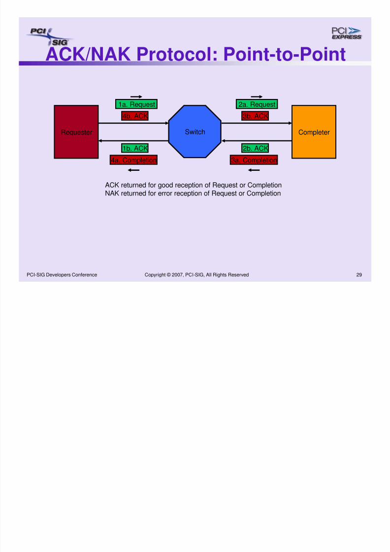
ACK returned for good reception of Request or CompletionNAK returned for error reception of Request or Completion
Requester Completer
1a. Request
Switch
2a. Request
3a. Completion4a. Completion
1b. ACK 2b. ACK
4b. ACK 3b. ACK
ACK/NAK Protocol: Point-to-Point
8/8/2019 Pcie Basics Pcisig
http://slidepdf.com/reader/full/pcie-basics-pcisig 30/40
Copyright © 2007, PCI-SIG, All Rights Reserved 30PCI-SIG Developers Conference
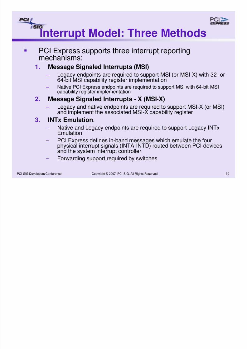
PCI Express supports three interrupt reportingmechanisms:
1. Message Signaled Interrupts (MSI) – Legacy endpoints are required to support MSI (or MSI-X) with 32- or
64-bit MSI capability register implementation
– Native PCI Express endpoints are required to support MSI with 64-bit MSIcapability register implementation
2. Message Signaled Interrupts - X (MSI-X) – Legacy and native endpoints are required to support MSI-X (or MSI)and implement the associated MSI-X capability register
3. INTx Emulation.
– Native and Legacy endpoints are required to support Legacy INTx
Emulation – PCI Express defines in-band messages which emulate the four
physical interrupt signals (INTA-INTD) routed between PCI devicesand the system interrupt controller
– Forwarding support required by switches
Interrupt Model: Three Methods
8/8/2019 Pcie Basics Pcisig
http://slidepdf.com/reader/full/pcie-basics-pcisig 31/40
Copyright © 2007, PCI-SIG, All Rights Reserved 31PCI-SIG Developers Conference
x
PCIe
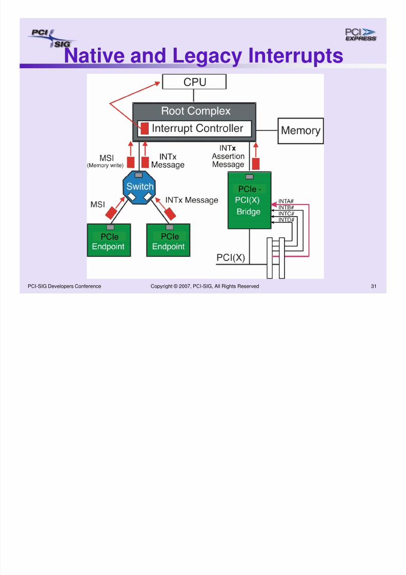
Native and Legacy Interrupts
PCIe
PCIe -
8/8/2019 Pcie Basics Pcisig
http://slidepdf.com/reader/full/pcie-basics-pcisig 32/40
Copyright © 2007, PCI-SIG, All Rights Reserved 32PCI-SIG Developers Conference
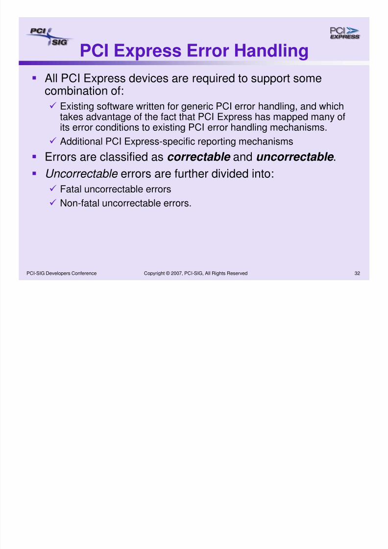
All PCI Express devices are required to support somecombination of:
Existing software written for generic PCI error handling, and whichtakes advantage of the fact that PCI Express has mapped many ofits error conditions to existing PCI error handling mechanisms.
Additional PCI Express-specific reporting mechanisms
Errors are classified as correctable and uncorrectable .
Uncorrectable errors are further divided into:
Fatal uncorrectable errors
Non-fatal uncorrectable errors.
PCI Express Error Handling
8/8/2019 Pcie Basics Pcisig
http://slidepdf.com/reader/full/pcie-basics-pcisig 33/40
Copyright © 2007, PCI-SIG, All Rights Reserved 33PCI-SIG Developers Conference
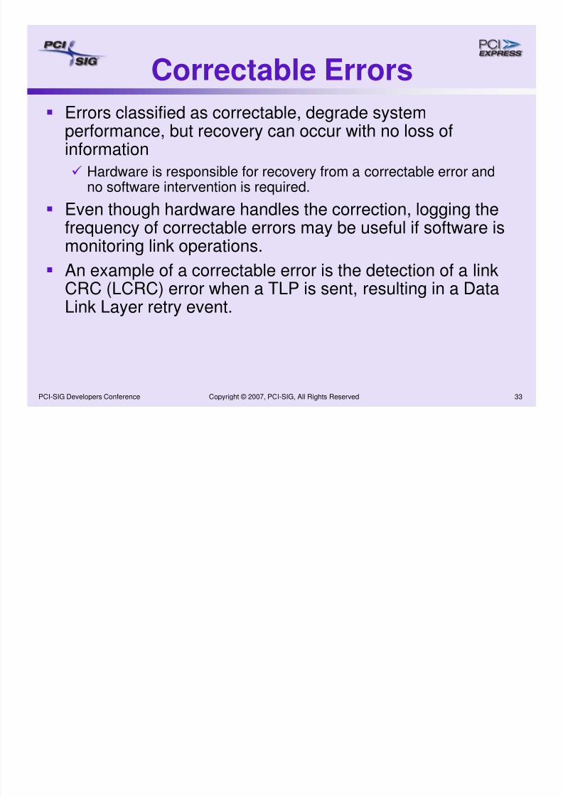
Errors classified as correctable, degrade systemperformance, but recovery can occur with no loss of
information Hardware is responsible for recovery from a correctable error and
no software intervention is required.
Even though hardware handles the correction, logging the
frequency of correctable errors may be useful if software ismonitoring link operations.
An example of a correctable error is the detection of a linkCRC (LCRC) error when a TLP is sent, resulting in a Data
Link Layer retry event.
Correctable Errors
8/8/2019 Pcie Basics Pcisig
http://slidepdf.com/reader/full/pcie-basics-pcisig 34/40
Copyright © 2007, PCI-SIG, All Rights Reserved 34PCI-SIG Developers Conference
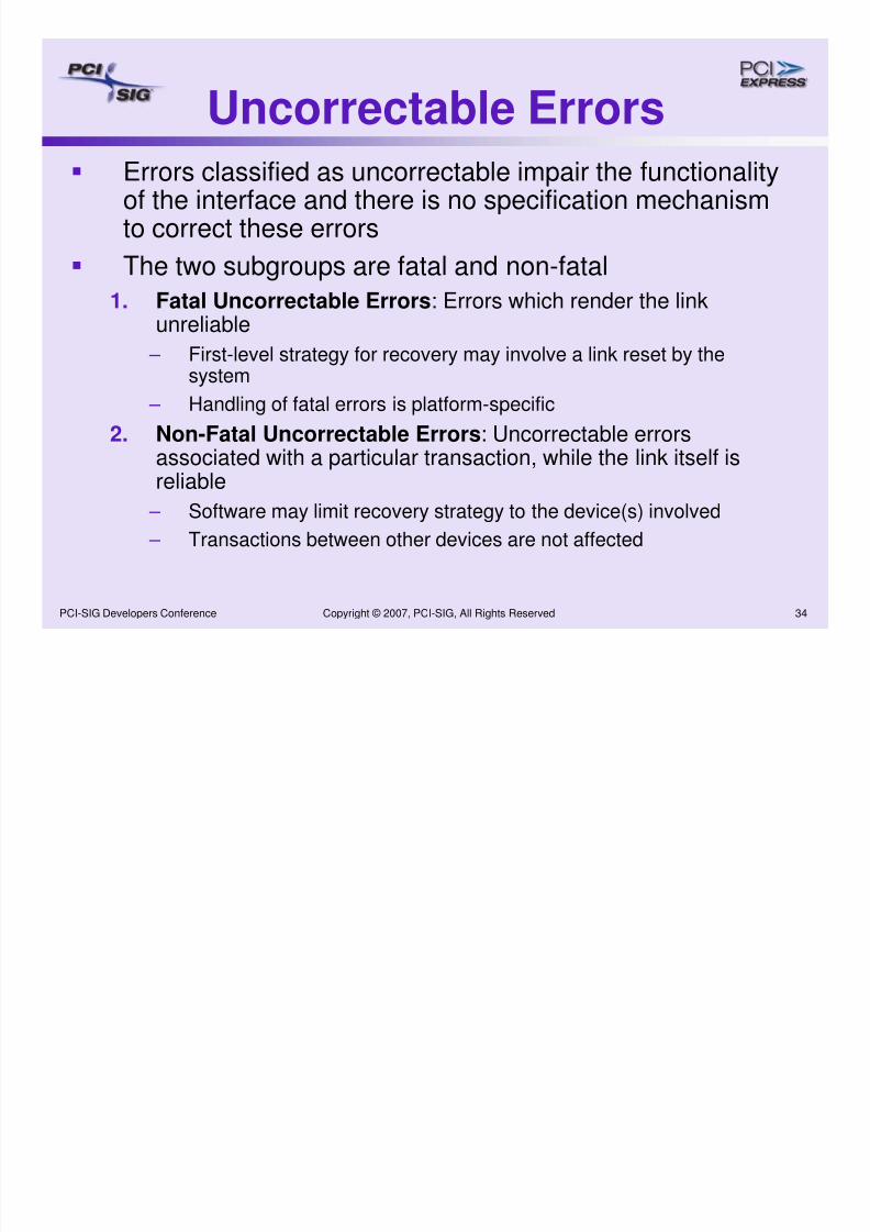
Errors classified as uncorrectable impair the functionalityof the interface and there is no specification mechanismto correct these errors
The two subgroups are fatal and non-fatal
1. Fatal Uncorrectable Errors: Errors which render the linkunreliable
– First-level strategy for recovery may involve a link reset by thesystem
– Handling of fatal errors is platform-specific
2. Non-Fatal Uncorrectable Errors: Uncorrectable errorsassociated with a particular transaction, while the link itself is
reliable – Software may limit recovery strategy to the device(s) involved
– Transactions between other devices are not affected
Uncorrectable Errors
8/8/2019 Pcie Basics Pcisig
http://slidepdf.com/reader/full/pcie-basics-pcisig 35/40
Copyright © 2007, PCI-SIG, All Rights Reserved 35PCI-SIG Developers Conference
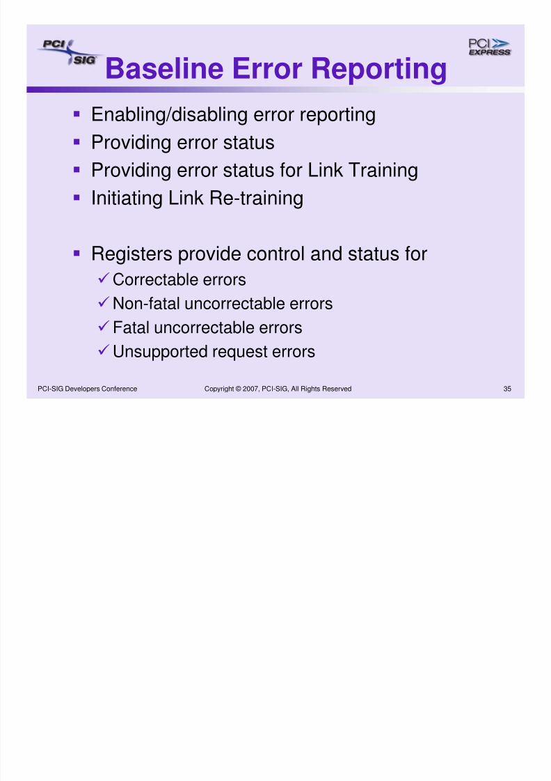
Enabling/disabling error reporting
Providing error status
Providing error status for Link Training
Initiating Link Re-training
Registers provide control and status for
Correctable errors
Non-fatal uncorrectable errorsFatal uncorrectable errors
Unsupported request errors
Baseline Error Reporting
8/8/2019 Pcie Basics Pcisig
http://slidepdf.com/reader/full/pcie-basics-pcisig 36/40
Copyright © 2007, PCI-SIG, All Rights Reserved 36PCI-SIG Developers Conference
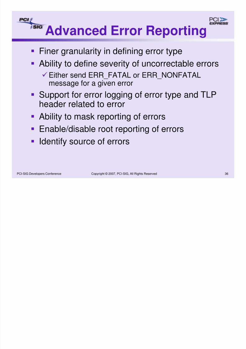
Finer granularity in defining error type
Ability to define severity of uncorrectable errors
Either send ERR_FATAL or ERR_NONFATALmessage for a given error
Support for error logging of error type and TLP
header related to error
Ability to mask reporting of errors
Enable/disable root reporting of errors
Identify source of errors
Advanced Error Reporting
PCI E
8/8/2019 Pcie Basics Pcisig
http://slidepdf.com/reader/full/pcie-basics-pcisig 37/40
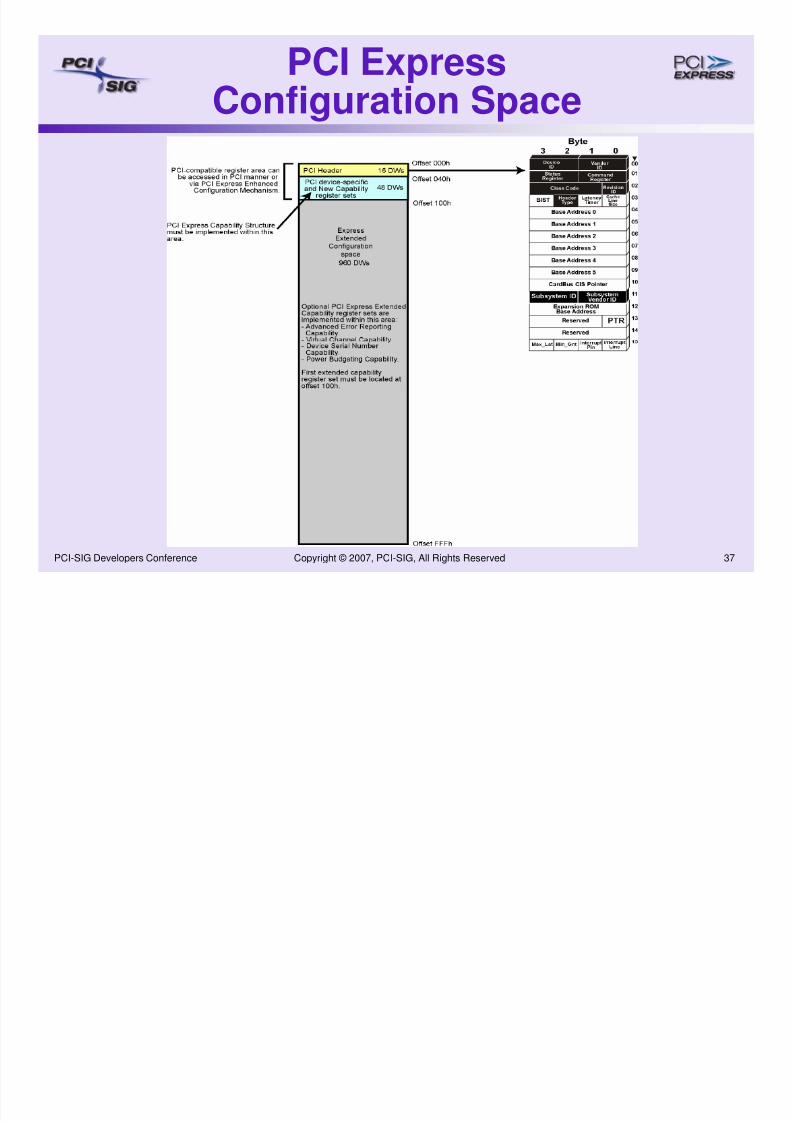
Copyright © 2007, PCI-SIG, All Rights Reserved 37PCI-SIG Developers Conference
PCI Express
Configuration Space
8/8/2019 Pcie Basics Pcisig
http://slidepdf.com/reader/full/pcie-basics-pcisig 38/40
Copyright © 2007, PCI-SIG, All Rights Reserved 38PCI-SIG Developers Conference
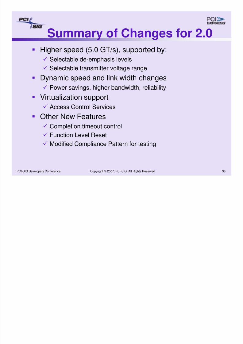
Summary of Changes for 2.0 Higher speed (5.0 GT/s), supported by:
Selectable de-emphasis levels
Selectable transmitter voltage range Dynamic speed and link width changes
Power savings, higher bandwidth, reliability
Virtualization support Access Control Services
Other New Features
Completion timeout control
Function Level Reset
Modified Compliance Pattern for testing

8/8/2019 Pcie Basics Pcisig
http://slidepdf.com/reader/full/pcie-basics-pcisig 39/40
Copyright © 2007, PCI-SIG, All Rights Reserved 39PCI-SIG Developers Conference
Thank you for attending thePCI-SIG Developers Conference 2007.
For more information please go towww.pcisig.com

8/8/2019 Pcie Basics Pcisig
http://slidepdf.com/reader/full/pcie-basics-pcisig 40/40
Copyright © 2007, PCI-SIG, All Rights Reserved 40
PCI Express BasicsPCI Express Basics
Ravi Budruk
Senior Staff Engineer and Partner
MindShare, Inc.
Ravi Budruk
Senior Staff Engineer and Partner
MindShare, Inc.